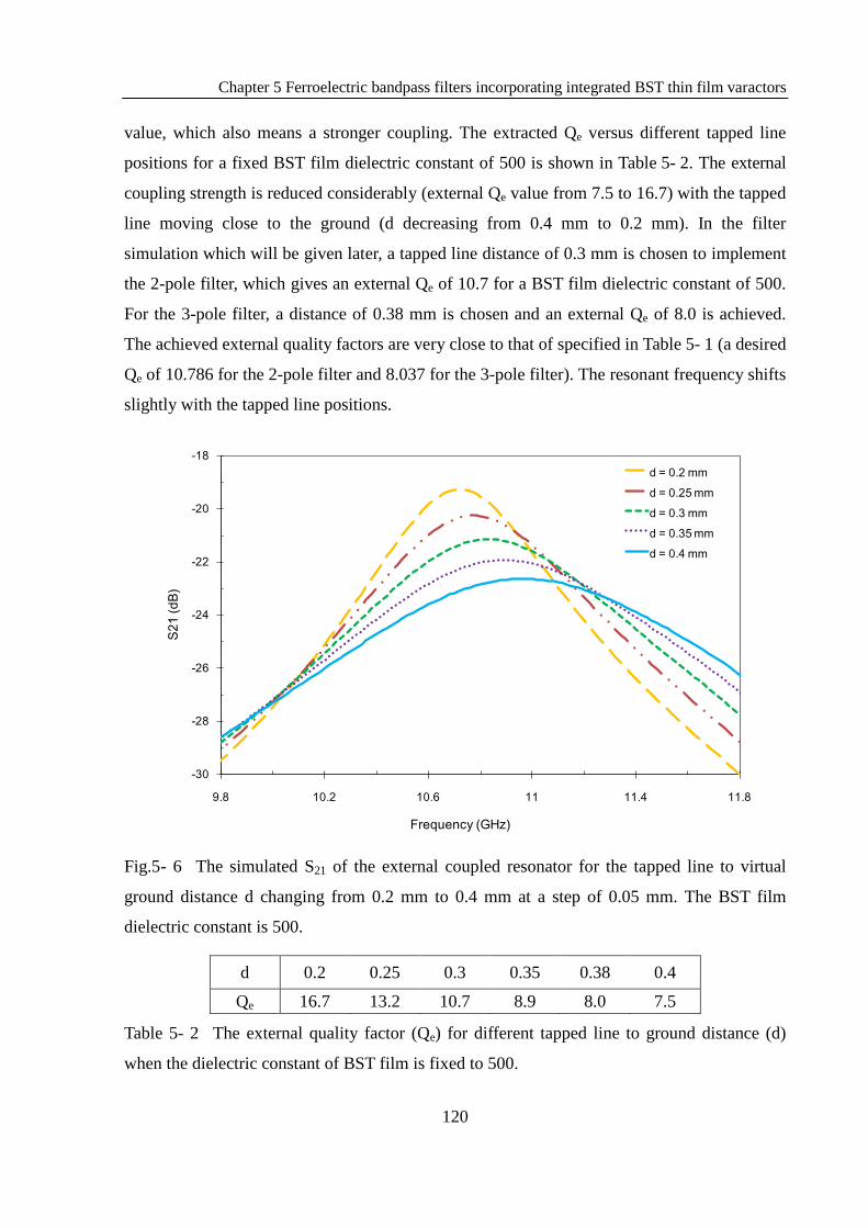
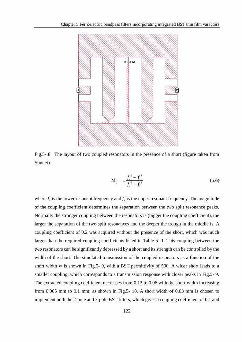
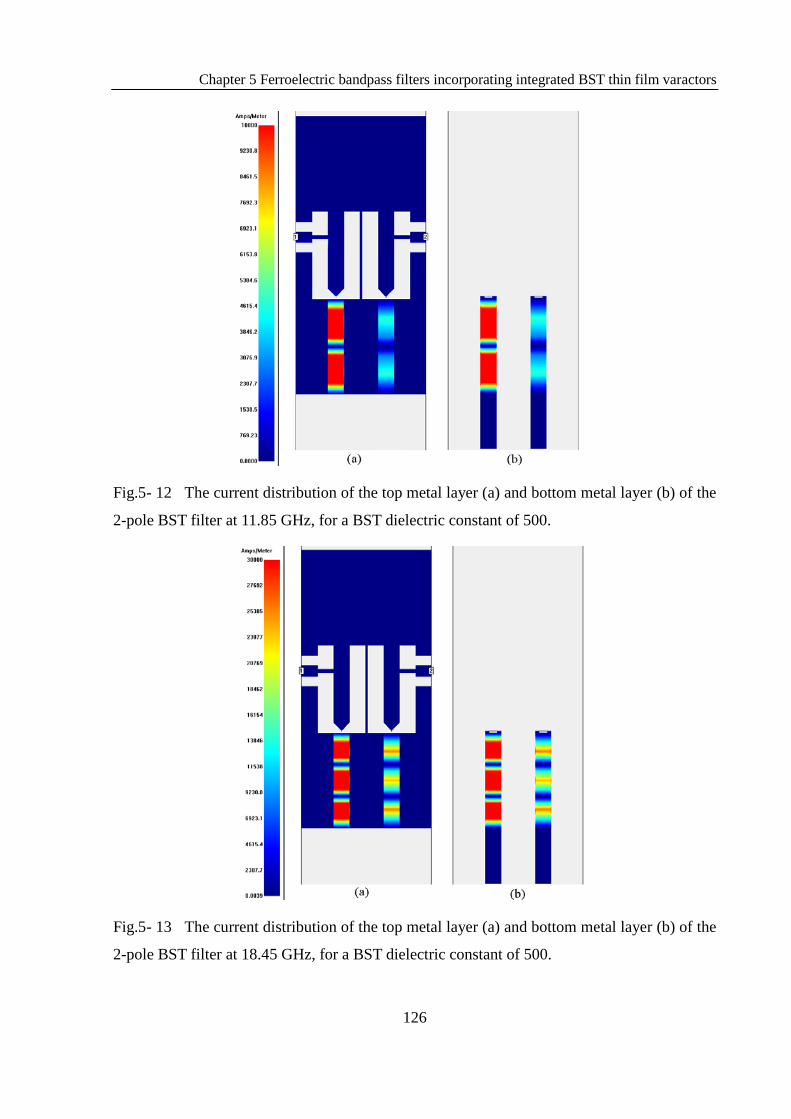
TUNABLE MICROWAVE FILTERS USING FERROELECTRIC THIN FILMS by XU WANG A thesis submitted to the Faculty of Engineering University of Birmingham For the degree of DOCTOR OF PHILOSOPHY School of Electronic, Electrical and Computer Engineering University of Birmingham Birmingham, B15 2TT United Kingdom October 2009
Transcript
TUNABLE MICROWAVE FILTERS USING FERROELECTRIC THIN FILMS
by
XU WANG
A thesis submitted to the Faculty of Engineering University of Birmingham
For the degree of DOCTOR OF PHILOSOPHY
School of Electronic, Electrical and Computer Engineering University of Birmingham Birmingham, B15 2TT United Kingdom October 2009
University of Birmingham Research Archive
e-theses repository This unpublished thesis/dissertation is copyright of the author and/or third parties. The intellectual property rights of the author or third parties in respect of this work are as defined by The Copyright Designs and Patents Act 1988 or as modified by any successor legislation. Any use made of information contained in this thesis/dissertation must be in accordance with that legislation and must be properly acknowledged. Further distribution or reproduction in any format is prohibited without the permission of the copyright holder.
SYNOPSIS
Frequency agile microwave devices based on Barium Strontium Titanate (BST) thin films
have gained a lot of interest in recent years. The frequency agility of the ferroelectric devices
is based on the external DC electric field controlled permittivity of BST thin film. In this
research work, several tunable microwave filters incorporating BST thin film varactors
operating in a frequency range between 1 GHz and 25 GHz are designed, tested and analysed.
In the thesis, the motivation for developing frequency agile devices is reviewed and several
technologies for tunable microwave filters are surveyed and compared. An introduction to the
background of ferroelectric materials and microwave properties of BST thin films is given.
Recent progress on the BST varactor and filters reported in the literature is reviewed and
compared with this work. Theoretical fundamentals for microwave filter design are outlined
as well.
The filters presented in this work are designed in a coplanar waveguide configuration on MgO
or high resistivity silicon substrates. Integrated or discrete BST varactors in either interdigital
or parallel plate configuration are employed as tuning elements. The filters design starts from
Chebyshev prototype filter synthesis, and follows by full wave electromagnetic (EM)
simulation by Sonnet. The multilayer BST filters are fabricated in house and tested using a
network analyser. The measurement results of these filters are analysed and compared well
with the EM simulation. The experimental performance shows that BST integrated filters
have miniaturised size and large tuning range at a DC bias less than 15 V, and the filters with
discrete BST varactors have a low insertion loss.
A lumped element lowpass filter incorporating integrated meander line inductors and BST
parallel plate capacitors is implemented on a high resistivity silicon substrate. 5 µm × 5 µm or
10 µm × 10 µm Ba0.25Sr0.75TiO3 thin film varactors are used as tuning elements. The filter loss
factors including the metal loss and BST loss are discussed. A tunability of 32.1 % of a BST
lowpass filter is recorded at 15 V. The lowpass filter can be treated as a switch, with 18 dB
isolation at around 25 GHz.
A combline bandpass filter employing line elements shorted at one end and loaded by BST
varactors at the opposite end as resonators is implemented on a MgO substrate. The
Ba0.6Sr0.4TiO3 thin film parallel plate capacitors are 5 µm × 5 µm in size. Each resonator can
be independently biased, which enables performance optimisation of the fabricated filter.
Etching of BST film is required to contact the bottom electrode. A two pole filter measured
shows a reasonable tuning from about 8 GHz to 12 GHz with 10 V bias of only one resonator.
The other resonator fails to tune as the top and bottom electrodes are shorted.
Two pole and four pole coupled resonator bandpass filters with discrete BST or GaAs
varactors as tuning elements are implemented in a frequency range of 1 - 3 GHz. BST
interdigital capacitors, BST parallel plate varactors, or GaAs varactors are integrated into a
microwave laminate circuit in a hybrid manner. A full set of measurement results is given. The
BST tuning technique is compared directly with the semiconductors in an application
environment for the first time. The filters based on BST parallel plate capacitors show an
insertion loss in line with the GaAs filters, which is also the lowest insertion loss of BST
filters ever reported.
Future work on improving the BST film and metal film loss at tens of gigahertz range is also
discussed.
To My Dad and Mom
ACKNOLEDGEMENTS
I would like to express my sincere gratitude to my supervisor Prof. Mike Lancaster, for
providing me the opportunity to study in the Emerging Device Technology (EDT) Research
Group, for generously guiding me throughout the research work, for constant encouragement,
quick reply, and full support of my study here. He has a wide range of research interest,
understands deep but expresses concisely. I benefit a lot from our meetings and his comments
on my thesis and papers.
I would also like to thank my co-supervisor Dr. Frederick Huang for many helpful advices on
device design and simulation, and correction of part of the thesis. I am also grateful to Dr. Tim
Jackson for his support on material fabrication and I appreciate his correction of the thesis and
papers very much. Special thanks go to my co-partner Dr. Peng Bao, who fabricates all the
ferroelectric devices in this project, for his hard work on material optimisation and device
fabrication, as well as many interesting ideas and discussion.
I would like to particularly thank Dr. Yi Wang and Dr. Guoyong Zhang for so much beneficial
discussion and help in device design and measurement, and for generously sharing their
experience. I also thank Donna Holdom and Dr. Maolong Ke for technical support on device
fabrication, and Clifford Ansell for manufacturing copper boxes for the devices. I am also
grateful to all my past and present colleagues in the EDT group for their advice, participation,
and help from time to time.
The project is a joint work with Heriot-Watt University and Cranfield University. I appreciate
the meetings and discussion with Dr. Jiasheng Hong, Dr. Young-Hoon Chun, Dr. Paul Kirby,
Arne Luker, Robert Wright from the two universities. I also appreciate the financial support
from the UK Engineering and Physics Science Research (EPSRC) scholarship.
Lastly and most importantly, I would like to acknowledge my parents. Love and trust from
you encouraged me in the past years. I could not have completed this thesis without you.
CONTENTS
Chapter 1 Introduction 1
1.1 Microwave frequencies 1
1.2 Motivation 2
1.3 Microwave tunable filters 4
1.4 Competing technologies 6
1.5 Thesis organisation 11
1.6 Summary 14
References 15
Chapter 2 Ferroelectric Materials and Devices 19
2.1 History and applications 19
2.2 Properties for microwave applications 25
2.3 BST deposition methods 31
2.4 Microwave characterisation techniques of ferroelectric thin films 36
2.5 Substrate choice 39
2.6 Metallisation choice 40
2.7 Ferroelectric varactors 43
2.8 Ferroelectric tunable filters 47
2.9 Other ferroelectric devices 51
2.10 Summary 52
References 53
Chapter 3 Microwave Filter Theory 61
3.1 Coplanar waveguide 61
3.1.1 Characteristic impedance and effective permittivity 62
3.1.2 Multilayer substrate coplanar waveguide 64
3.1.3 Guided wavelength, phase velocity and electrical length 67
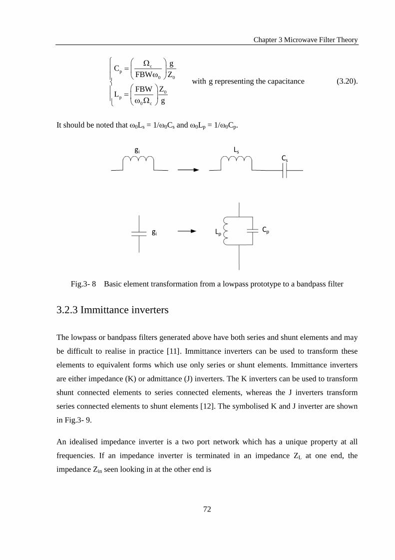
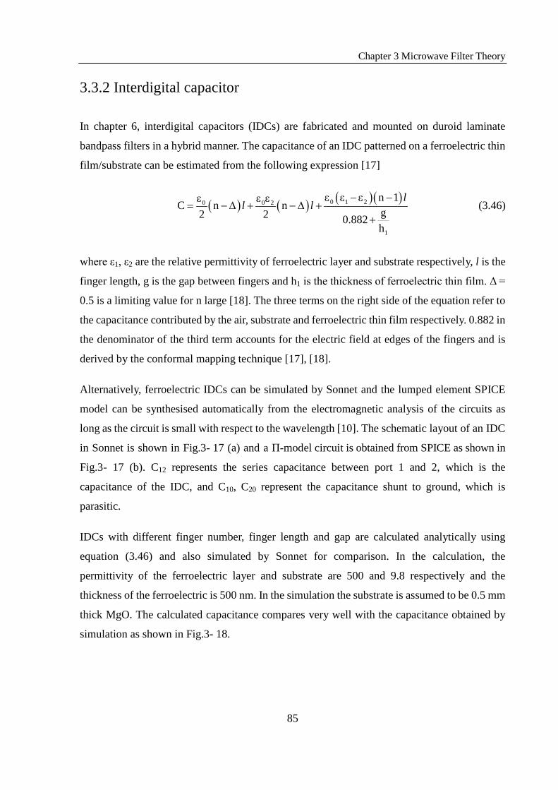
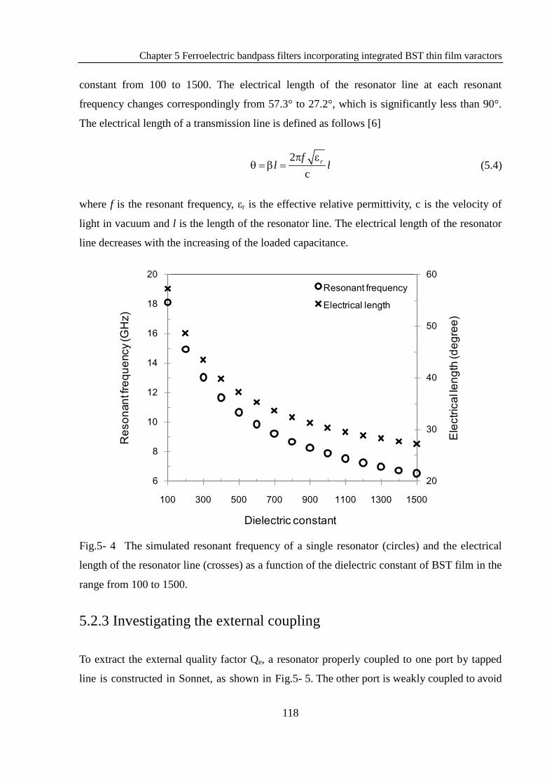
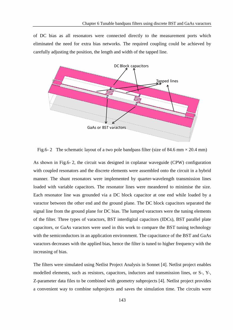
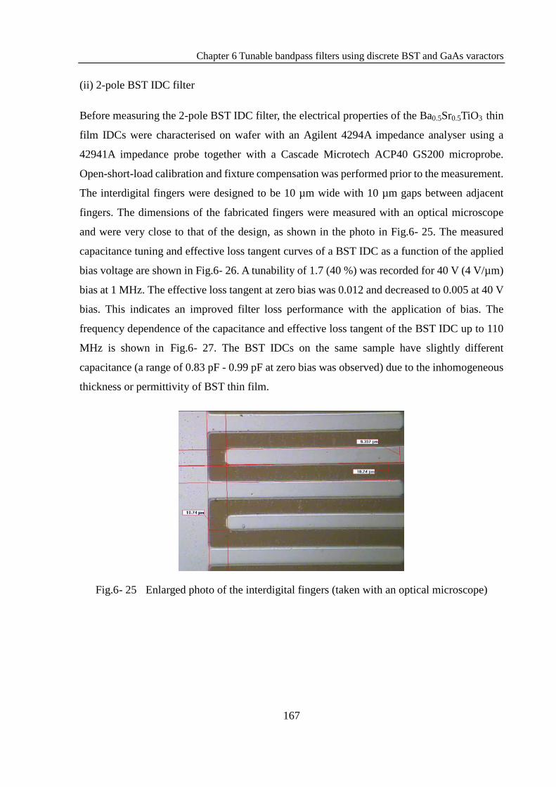
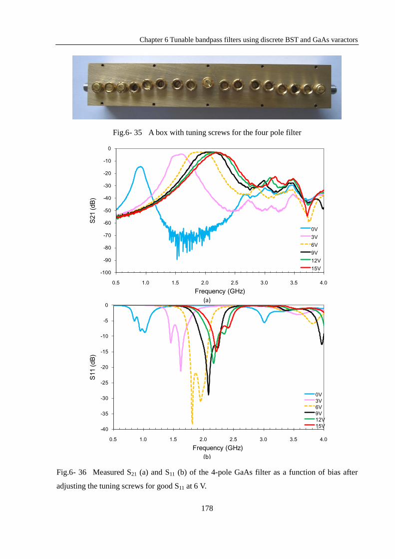
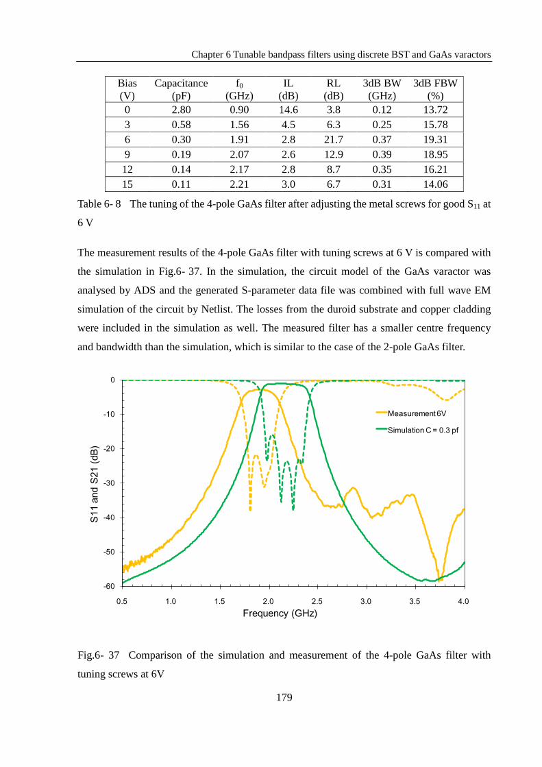
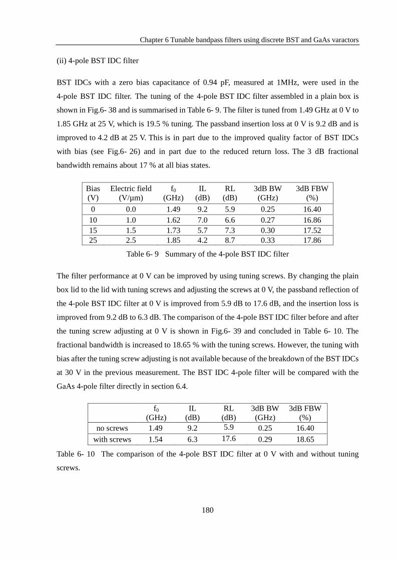
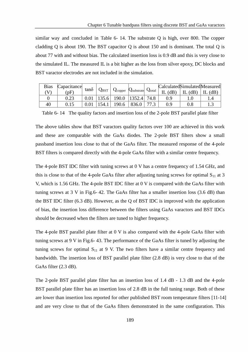
or BST parallel plate capacitors were fabricated in house, characterised using an impedance
analyser, and assembled into the filter circuits in a hybrid manner. The same filters were also
made using commercially available GaAs varactors to give a direct comparison between the
BST and semiconductor tuning techniques in an application environment. These varactors
performed as tuning elements in the filters. The two pole BST IDC filter was tuned from a
centre frequency of 1.55 GHz and an insertion loss of 3.7 dB at zero bias, to 2.02 GHz and 1.1
dB with 65 V bias, which made a figure of merit (FoM) of 0.87 dB-1. The two pole BST
parallel plate filter was tuned from 2.32 GHz at zero bias to 2.52 GHz at 45 V bias, with an
insertion loss of 1.4 dB to 1.3 dB correspondingly. The filter showed a FoM of 0.41 dB-1. The
two pole GaAs filter showed the largest tuning range from 0.94 GHz to 2.44 GHz with 14 V
bias and a FoM of 3.84 dB-1, as a result of the high tunability of the GaAs varactors. The four
pole filters showed a tuning range close to that of the two pole ones with the same kind of
varactors. The BST filters demonstrated a loss performance in line with the GaAs filters in the
gigahertz range.
Finally, the thesis is concluded in the last chapter and direction for future work is also
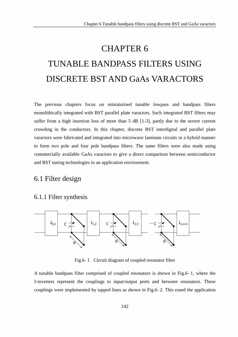
Chapter 1 Introduction
14
presented.
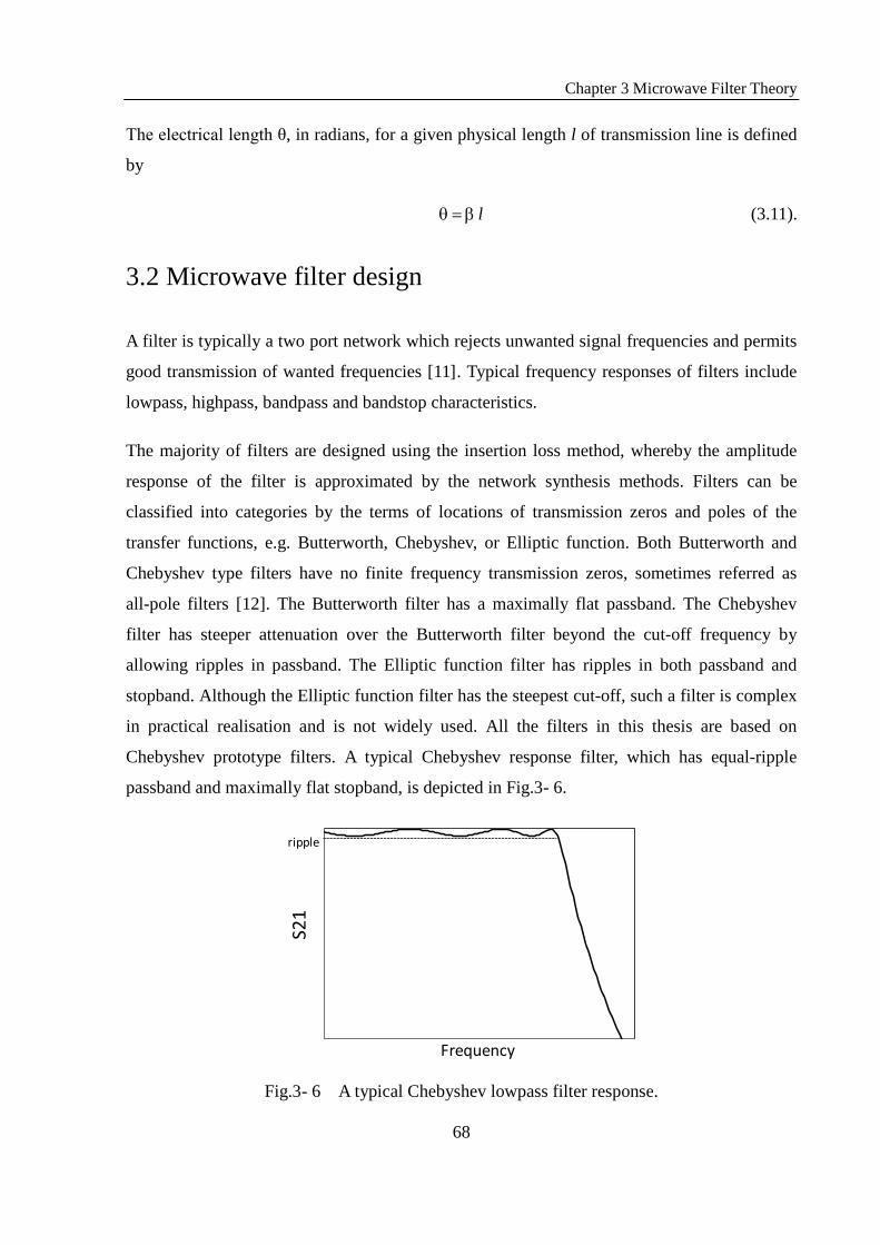
1.6 Summary
In this chapter the motivation to developing microwave tunable filters was described and
some characteristic parameters of tunable filters were introduced. The current and promising
technologies for frequency agile devices were discussed and compared. At the end, the thesis
organisation was introduced and the following chapters were overviewed.
Chapter 1 Introduction
15
References
[1] http://safetycenter.navy.mil/acquisition/RFR. [2] D. M. Pozar, Microwave Engineering, 2nd ed. New York, USA, John Wiley & Sons,
Inc., 1998. [3] Radio Frequency Band Designations, http://www.radioing.com/eengineer/index.html. [4] K. Chang, "Microwave passive and antenna components", in Handbook of microwave
and optical components. vol. 1: John Wiley & Sons, Inc., 1989. [5] J. Nath, D. Ghosh, J. P. Maria, A. I. Kingon, W. Fathelbab, P. D. Franzon, and M. B.
Steer, "An electronically tunable microstrip bandpass filter using thin-film Barium-Strontium-Titanate (BST) varactors", IEEE Transactions on Microwave Theory and Techniques, vol. 53, no. 9, pp. 2707-2712, 2005.
[6] S.-J. Park, "High-Performance RF-MEMS Tunable Filters", Doctor of Philosophy thesis, Electrical Engineering, The University of Michigan, 2008
[7] J. Ryynanen, S. Lindfors, K. Stadius, and K. A. I. Halonen, "Integrated circuits for multiband multimode receivers", Circuits and Systems Magazine, vol. 6, no. 2, pp. 5-16, 2006.
[8] J. Nath, "Design and characterization of frequency agile RF and microwave devices using ferroelectrics", Doctor of Philosophy thesis, Electrical Engineering, North Carolina State University, 2006
[9] J. Ryynanen, K. Kivekas, J. Jussila, L. Sumanen, A. Parssinen, and K. A. I. Halonen, "A single-chip multimode receiver for GSM900, DCS1800, PCS1900, and WCDMA", IEEE Journal of Solid-State Circuits, vol. 38, no. 4, pp. 594-602, 2003.
[10] M. Owens, "Frequency agile system for naval target control": http://www.dtic.mil/dtic, 2005.
[11] J. Mitola and G. Q. Maguire, "Cognitive radio: making software radios more personal", IEEE Personal Communications, vol. 6, no. 4, pp. 13-18, 1999.
[12] A. F. Molisch, L. J. Greenstein, and M. Shafi, "Propagation Issues for Cognitive Radio", Proceedings of the IEEE, vol. 97, no. 5, pp. 787-804, 2009.
[13] NTIA, "The radio spectrum frequency allocations": http://www.ntia.doc.gov/osmhome/allochrt.pdf, 2003.
[14] A. E. Leu, B. L. Mark, and M. A. McHenry, "A Framework for Cognitive WiMAX With Frequency Agility", Proceedings of the IEEE, vol. 97, no. 4, pp. 755-773, 2009.
[15] R. M. Young, J. D. Adam, C. R. Vale, T. T. Braggins, S. V. Krishnaswamy, C. E. Milton, D. W. Bever, L. G. Chorosinski, C. Li-Shu, D. E. Crockett, C. B. Freidhoff, S. H. Talisa, E. Capelle, R. Tranchini, J. R. Fende, J. M. Lorthioir, and A. R. Tories, "Low-loss bandpass RF filter using MEMS capacitance switches to achieve a one-octave tuning range and independently variable bandwidth", in IEEE MTT-S International Microwave Symposium Digest2003, pp. 1781-1784 vol.3.
[16] R. E. Collin, Foundations for Microwave Engineering, McGraw-Hill, 1992. [17] I. C. Hunter and J. D. Rhodes, "Electronically tunable microwave bandpass filters",
IEEE Transactions on Microwave Theory and Techniques, vol. 82, no. 9, pp. 1354-1360, 1982.
[18] Y. Ming, "Power-handling capability for RF filters", Microwave Magazine, vol. 8, no. 5, pp. 88-97, 2007.
[19] J. Uher and W. J. R. Hoefer, "Tunable microwave and millimeter-wave band-pass
Chapter 1 Introduction
16
filters", IEEE Transactions on Microwave Theory and Techniques, vol. 39, no. 4, pp. 643-653, 1991.
[20] A. G. Fox, "An Adjustable Wave-Guide Phase Changer", Proceedings of the IRE, vol. 35, no. 12, pp. 1489-1498, 1947.
[21] G.L.Matthaei, L.Young, and E.M.T.Jones, Microwave filters, impedance matching networks, and coupling structures, Artech House, 1980.
[22] F. Reggia and E. G. Spencer, "A New Technique in Ferrite Phase Shifting for Beam Scanning of Microwave Antennas", Proceedings of the IRE, vol. 45, no. 11, pp. 1510-1517, 1957.
[23] H. Brand and N. Krause, "Tunable millimetre-wave ferrite bandpass filter with reduced biasing field", Electronics Letters, vol. 13, no. 19, pp. 576-578, 1977.
[24] G. Leon, R. R. Boix, and F. Medina, "Tunability and bandwidth of microstrip filters fabricated on magnetized ferrites", Microwave and Wireless Components Letters, vol. 14, no. 4, pp. 171-173, 2004.
[25] J. Krupka, A. Abramowicz, and K. Derzakowski, "Magnetically tunable filters for cellular communication terminals", IEEE Transactions on Microwave Theory and Techniques, vol. 54, no. 6, pp. 2329-2335, 2006.
[26] J. D. Adam, L. E. Davis, G. F. Dionne, E. F. Schloemann, and S. N. Stitzer, "Ferrite devices and materials", IEEE Transactions on Microwave Theory and Techniques, vol. 50, no. 3, pp. 721-737, 2002.
[27] P. S. Carter, "Magnetically-tunable microwave filters using single-crystal yttrium-iron-garnet resonators", IRE Transactions on Microwave Theory and Techniques, no. pp. 252-260, 1960.
[28] Varactor / varicap diode, www.radio-electronics.com. [29] C. B. Hofmann and A. R. Baron, "Wideband ESM receiving systems-Part I",
Microwave J., vol. 23, no. 9, pp. 24-34, Sep,1980. [30] A. Vorobiev, P. Rundqvist, K. Khamchane, and S. Gevorgian, "Silicon substrate
integrated high Q-factor parallel-plate ferroelectric varactors for microwave/millimeterwave applications", Applied Physics Letters, vol. 83, no. 15, pp. 3144-3146, 2003.
[31] Microwave Device Technology Ltd., http://www.microwavedevicetechnology.com. [32] L. E. Larson, R. H. Hackett, M. A. Melendes, and R. F. Lohr, "Micromachined
microwave actuator (MIMAC) technology-a new tuning approach for microwave integrated circuits", in Microwave and Millimeter-Wave Monolithic Circuits Symposium, 1991. Digest of Papers, IEEE 19911991, pp. 27-30.
[33] A. Dec and K. Suyama, "Micromachined electro-mechanically tunable capacitors and their applications to RF IC's", IEEE Transactions on Microwave Theory and Techniques, vol. 46, no. 12, pp. 2587-2596, 1998.
[34] C. L. Goldsmith, Y. Zhimin, S. Eshelman, and D. Denniston, "Performance of low-loss RF MEMS capacitive switches", Microwave and Guided Wave Letters, vol. 8, no. 8, pp. 269-271, 1998.
[35] K. Entesari and G. M. Rebeiz, "A 12-18-GHz Three-Pole RF MEMS Tunable Filter", IEEE Transactions on Microwave Theory and Techniques, vol. 53, no. 8, pp. 2566-2571, 2005.
[36] Y. Jun-Bo and C. T. C. Nguyen, "A high-Q tunable micromechanical capacitor with movable dielectric for RF applications", in Electron Devices Meeting Technical Digest2000, pp. 489-492.
[37] T. K. K. Tsang and M. N. El-Gamal, "Micro-electromechanical variable capacitors for
Chapter 1 Introduction
17
RF applications", in the 45th Midwest Symposium on Circuits and Systems2002, pp. 25-28.
[38] J. Y. Park, Y. J. Yee, H. J. Nam, and J. U. Bu, "Micromachined RF MEMS tunable capacitors using piezoelectric actuators", in IEEE MTT-S International Microwave Symposium Digest2001, pp. 2111-2114.
[39] Z. Feng, H. Zhang, K. C. Gupta, W. Zhang, V. M. Bright, and Y. C. Lee, "MEMS-based series and shunt variable capacitors for microwave and millimeter-wave frequencies", Sensors and Actuators A: Physical, vol. 91, no. pp. 256-265, 2001.
[40] A. Abbaspour-Tamijani, L. Dussopt, and G. M. Rebeiz, "Miniature and tunable filters using MEMS capacitors", IEEE Transactions on Microwave Theory and Techniques, vol. 51, no. 7, pp. 1878-1885, 2003.
[41] K. Hong-Teuk, P. Jae-Hyoung, K. Yong-Kweon, and Youngwoo Kwon, "Low-loss and compact V-band MEMS-based analog tunable bandpass filters", Microwave and Wireless Components Letters, vol. 12, no. 11, pp. 432-434, 2002.
[42] E. Marsan, J. Gauthier, M. Chaker, and K. Wu, "Tunable microwave device: status and perspective", in IEEE-NEWCAS Conference2005, pp. 279-282.
[43] A.K.Tagantsev, V.O.Sherman, K.F.Astafiev, J.Venkatesh, and N.Setter, "Ferroelectric materials for microwave tunable applications", Journal of Electroceramics, vol. 11, no. pp. 5-66, 2003.
[44] D. Kuylenstierna, E. Ash, A. Vorobiev, T. Itoh, and S. Gevorgian, "X-band Left Handed Phase Shifter using Thin Film Ba0.25Sr0.75TiO3 Ferroelectric Varactors", in the 36th European Microwave Conference2006, pp. 847-850.
[45] K. B. Kim, T. S. Yun, J. C. Lee, M. Chaker, C. S. Park, and K. Wu, "Integration of microwave phase shifter with BST varactor onto TiO/sub 2//Si wafer", Electronics Letters, vol. 43, no. 14, 2007.
[46] L. Y. V. Chen, R. Forse, D. Chase, and R. A. York, "Analog tunable matching network using integrated thin-film BST capacitors", in IEEE MTT-S International Microwave Symposium Digest2004, pp. 261-264.
[47] D. Kuylenstierna, A. Vorobiev, P. Linner, and S. Gevorgian, "Ultrawide-band tunable true-time delay lines using ferroelectric varactors", IEEE Transactions on Microwave Theory and Techniques, vol. 53, no. 6, pp. 2164-2170, 2005.
[48] P. Bao, T. J. Jackson, X. Wang, and M. J. Lancaster, "Barium strontium titanate thin film varactors for room-temperature microwave device applications", Journal of Physics D: Applied Physics, vol. 41, no. p. 063001, 2008.
[49] A. Tombak, F. Tito Ayguavives, J. P. Maria, G. T. Stauf, A. I. Kingon, and A. Mortazawi, "Low voltage tunable barium strontium titanate thin film capacitors for RF and microwave applications", in IEEE MTT-S International Microwave Symposium Digest2000, pp. 1345-1348 vol.3.
[50] T. Ayguavives, A. Tombak, J. P. Maria, G. T. Stauf, C. Ragaglia, J. Roeder, A. Mortazawi, and A. I. Kingon, "Physical properties of (Ba,Sr)TiO3 thin films used for integrated capacitors in microwave applications", in Proceedings of the12th IEEE International Symposium on Applications of Ferroelectrics2000, pp. 365-368.
[51] R. York, A. Nagra, E. Erker, T. Taylor, P. Periaswamy, J. Speck, S. Streiffer, and O. Auciello, "Microwave integrated circuits using thin-film BST", in Proceedings of the 12th IEEE International Symposium on Applications of Ferroelectrics2000, pp. 195-200 vol. 1.
[52] O. G. Vendik, E.K.Hollmann, A. B. Kozyrev, and A. M. Prudan, "Ferroelectric tuning
Chapter 1 Introduction
18
of planar and bulk microwave devices", Journal of Superconductivity, vol. 12, no. pp. 325-338, 1999.
[53] M. S. Tsai, S. C. Sun, and T.-Y. Tseng, "Effect of bottom electrode materials on the electrical and reliability characteristics of (Ba, Sr)TiO3 capacitors", IEEE Transactions on Electron Devices, vol. 46, no. 9, pp. 1829-1838, 1999.
[54] A. Vorobiev, P. Rundqvist, K. Khamchane, and S. Gevorgian, "Microwave loss mechanisms in Ba0.25Sr0.75TiO3 thin film varactors", Journal of Applied Physics, vol. 96, no. 8, pp. 4642-4649, 2004.
[55] D. Ghosh, B. Laughlin, J. Nath, A. I. Kingon, M. B. Steer, and J. P. Maria, "Tunable high-quality-factor interdigitated (Ba, Sr)TiO3 capacitors fabricated on low-cost substrates with copper metallization", Thin Solid Films, vol. 496, no. 2, pp. 669-673, 2006.
[56] C. Lugo, G. Wang, J. Papapolymerou, Z. Zhao, X. Wang, and A. T. Hunt, "Frequency and Bandwidth Agile Millimeter-Wave Filter Using Ferroelectric Capacitors and MEMS Cantilevers", IEEE Transactions on Microwave Theory and Techniques, vol. 55, no. 2, pp. 376-382, 2007.
[57] W. Sichak and H. Augenblick, "Tunable Waveguide Filters", Proceedings of the IRE, vol. 39, no. 9, pp. 1055-1059, 1951.
[58] H. L. Bachman and H. A. Wheeler, "Evacuated Waveguide Filter for Suppressing Spurious Transmission from High-Power S-Band Radar", IRE Transactions on Microwave Theory and Techniques, vol. 7, no. 1, pp. 154-162, 1959.
Chapter 2 Ferroelectric Materials and Devices
19
CHAPTER 2
FERROELECTRIC MATERIALS AND
DEVICES
This chapter covers the history, fundamental properties, fabrication issues, measurement
techniques and applications of ferroelectric materials, with emphasis on ferroelectric thin
films for microwave applications. Ferroelectric microwave devices are reviewed and surveys
of BST varactors and bandpass filters are presented.
2.1 History and applications
Ferroelectric materials, which are a subset of piezoelectric and pyroelectric materials, exhibit
an electric field re-orientable spontaneous polarisation in a certain temperature range. The
spontaneous polarisation is highly temperature dependent and disappears above a phase
transition temperature Tph, where the material is said to be in the paraelectric phase. When the
temperature decreases below Tph, the crystal structure exhibits a slight deformation, the centre
of positive charge and negative charge does not coincide, thus electric dipoles are formed and
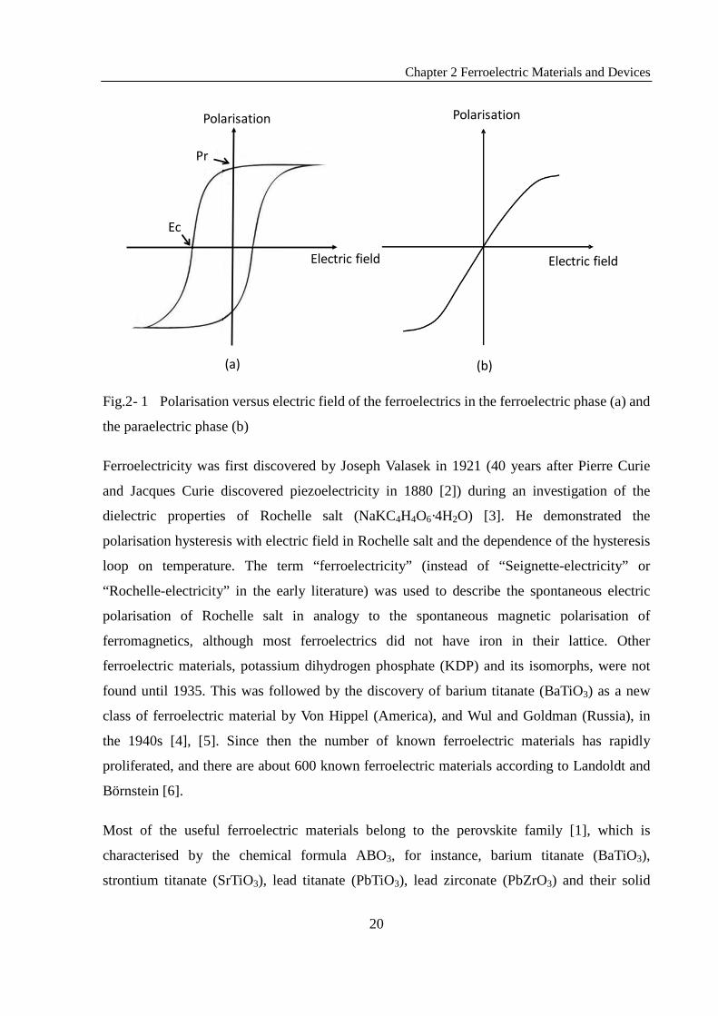
spontaneous polarisation appears in the ferroelectric phase [1].
In the paraelectric phase, the polarisation is proportional to the external electric field. In the
ferroelectric phase, the polarisation does not return back to zero when the external field is
zero and exhibits remanent polarisation Pr. A coercive field Ec is needed to bring the
polarisation back to zero [1]. Hence a polarisation-electric field (P-E) hysteresis loop is
observed in ferroelectric phase. The polarisation as a function of electric field of the
ferroelectric material in ferroelectric and paraelectric phases is shown in Fig.2- 1.
Chapter 2 Ferroelectric Materials and Devices
20
Polarisation Polarisation
Electric field Electric field
Pr
Ec
(a) (b)
Fig.2- 1 Polarisation versus electric field of the ferroelectrics in the ferroelectric phase (a) and
the paraelectric phase (b)
Ferroelectricity was first discovered by Joseph Valasek in 1921 (40 years after Pierre Curie
and Jacques Curie discovered piezoelectricity in 1880 [2]) during an investigation of the
dielectric properties of Rochelle salt (NaKC4H4O6·4H2O) [3]. He demonstrated the
polarisation hysteresis with electric field in Rochelle salt and the dependence of the hysteresis
loop on temperature. The term “ferroelectricity” (instead of “Seignette-electricity” or
“Rochelle-electricity” in the early literature) was used to describe the spontaneous electric
polarisation of Rochelle salt in analogy to the spontaneous magnetic polarisation of
ferromagnetics, although most ferroelectrics did not have iron in their lattice. Other
ferroelectric materials, potassium dihydrogen phosphate (KDP) and its isomorphs, were not
found until 1935. This was followed by the discovery of barium titanate (BaTiO3) as a new
class of ferroelectric material by Von Hippel (America), and Wul and Goldman (Russia), in
the 1940s [4], [5]. Since then the number of known ferroelectric materials has rapidly
proliferated, and there are about 600 known ferroelectric materials according to Landoldt and
Börnstein [6].
Most of the useful ferroelectric materials belong to the perovskite family [1], which is
characterised by the chemical formula ABO3, for instance, barium titanate (BaTiO3),
strontium titanate (SrTiO3), lead titanate (PbTiO3), lead zirconate (PbZrO3) and their solid
Chapter 2 Ferroelectric Materials and Devices
21
solutions. Fig.2- 2 shows the cubic cell structure of ABO3 type materials, with A2+ ions (green)
at the apices, B4+ (blue) ions at the centre, and O2- (red) ions at the face centres of the cube. It
is well known that the ABO3 structure permits variable compositions by substitution on A- or
B- sites by radius compatible ions [7], [8]. When applying an electric field, both B4+ cations
and O2- anions shift from their equilibrium positions and form electric dipoles as shown in
Fig.2- 3. In the paraelectric phase, the ions return to their initial equilibrium positions after the
electric field is removed. When T < Tph, a ferroelectric phase is exhibited, the ions undergo a
spontaneous displacement in the absence of an electric field and remain permanently
displaced [9].
Fig.2- 2 Cubic Cell of ABO3 type material (taken from [7])
E = 0
-
+Dipole
E ≠ 0
Fig.2- 3 Rearrangement of unit cell in response to an external electric field and formation of a
dipole (taken from [10])
Chapter 2 Ferroelectric Materials and Devices
22
Bulk ferroelectrics have found a wide spread usage as dielectrics, piezoelectrics, pyroelectrics
and ferroelectrics in the electronic industry for more than 50 years. Prominent examples
include the widely used multilayer ceramic capacitors, which use barium titanate as dielectrics,
and the positive temperature coefficient resistors (PTCRs) using appropriately doped barium
titanate in thermistors and self-regulating heating systems [11]. Piezoelectric/pyroelectric
ceramics are widely used in various sensing and actuating applications [1]. For instance,
ultrasonic transducers, which use the piezoelectricity of lead zirconium titanate ceramics, are
used in many sonar and depth sounding systems.
Applications of ferroelectrics in the form of thin films did not emerge until the 1980s [12].
The initial interest of developing ferroelectric thin films started in the late sixties, with the
non-volatile memory as the main driving application [13-15], however, this attempt was
frustrated due to the limitations of both material fabrication technology and device electronics
at that time. The interest in ferroelectric thin films was renewed due to both the advance in
thin film deposition techniques in the mid-eighties and the increasing requirement for
miniaturised systems [16], [17]. The current and potential application domains of thin film
ferroelectrics include memories, microsystems with pyroelectric and piezoelectric
microsensors/actuators, and microwave tunable devices [15].
Non-volatile ferroelectric memory (FeRAM) might be one of the most attractive applications
of ferroelectrics. FeRAM has a similar construction to conventional dynamic random access
memory (DRAM), but uses a ferroelectric layer to achieve non-volatility. An electric field is
used to switch, or “write”, each ferroelectric cell into either a positive or negative polarisation
state, representing either “0” or “1” in binary encoding. FeRAM shows attractive features
such as low power consumption compared with conventional DRAM and fast write speed
over flash memory. FeRAMs have now become a commercially viable option as low density
memories in smart cards [18]. Another important memory application is ferroelectric dynamic
random access memory. The cell size and capacitor size can be progressively reduced by the
use of high dielectric constant ferroelectrics as a replacement of SiO2/Si3N4 in conventional
DRAMs.
Ferroelectric thin films have also found applications in the recently emerged area of
micro-electro-mechanical systems (MEMS) due to their strong piezoelectric and pyroelectric
Chapter 2 Ferroelectric Materials and Devices
23
effect [19]. Ferroelectric films, typically PZT, can be deposited on the substrate prior to the
microfabrication to add sensing and actuating functionalities to microdevices [15]. Various
devices have been intensively researched during the past decade, such as accelerometers [20],
micromotors [21], ultrasonic transducers for medical imaging [22] and sensors and actuators
in atomic force microscopy (AFM) [23].
Ferroelectric thin film based microwave tunable devices have received intensive attention in
recent years, and are the focus of this thesis. The material property that makes ferroelectric
tuning possible is the electric field controlled dielectric constant. The basic concept was not
new; being first proposed back in the 1960s [24], [25]. However, the difficulties of matching
the reactance of the bulk ferroelectric varactors to the impedance of the rest of the circuit and
the requirement for high tuning voltage impeded its development [26]. The interest was then
moved to the development of thin film ferroelectrics on dielectric substrates, which provided
suitable capacitance values and could be tuned at modest voltage levels. However, such
samples suffered from a prohibitively high loss tangent [27]. The applications of ferroelectric
thin films were only beginning to emerge from the late eighties [12]. This was in large part
due to the advances in ferroelectric thin film deposition techniques [16], [17] and the ability to
integrate ferroelectrics with semiconductor technologies [15], and perhaps also encouraged by
the discovery of high-temperature superconducting oxides (i.e. YBCO), which had similar
crystal structure (perovskite type) to ferroelectrics [28] and enabled further miniaturisation.
Since then various ferroelectric varactors, tunable filters and resonators, phase shifters,
tunable matching networks and delay lines have been demonstrated with high performance in
the past decades.
SrTiO3 (STO) and BaxSr1-xTiO3 (BST) thin films are two of the most popular ferroelectrics for
electric tuning applications. The paraelectric phase is often preferred for microwave tuning
applications because of the absence of hysteresis and lower dielectric loss [29]. STO, which is
an incipient ferroelectric, is in the paraelectric phase at the boiling temperature of liquid
nitrogen. The structure and processing compatibility of STO and high-temperature
superconductors (HTS) has enabled a variety of cryogenic microwave devices since the 1990s
[30-40]. However, STO has little tunability at room temperature. Application of such devices
is limited as they need to be cooled down to cryogenic temperature. BaxSr1-xTiO3, which has
good tunability and reasonable loss at room temperature, can overcome this problem. The
Chapter 2 Ferroelectric Materials and Devices
24
Curie temperature Tc of BaxSr1-xTiO3 can be continuously shifted from about 40 K to 385 K
by tailoring the Ba to Sr ratio in the composition (see Fig.2- 4). Examples of the published
BST thin film varactors and tunable filters will be summarised in sections 2.7 and 2.8.
An overview of the main application areas of ferroelectrics and the underlying behaviour
exploited is given in Fig.2- 5. The microwave dielectric properties of ferroelectric materials
will be discussed in the next section with emphasis on BST thin films.
0
100
200
300
400
0.0 0.2 0.4 0.6 0.8 1.0
T c(K
)
x
Fig.2- 4 Curie temperature (Tc) as a function of Ba concentration (x) for BaxSr1-xTiO3 [10]
FerroelectricsCeramic capacitors
Non-volatile memory
P-E hysteresis
Microwave tunable devices
Field dependentdielectric constant
Piezoelectricity
DRAM
Electro-optic
Optical waveguidesOptical memories and displays
High dielectricconstant
Pyroelectric detector
Sensors, actuators,transducers, transformers,
Pyroelectricity
Fig.2- 5 Overview of major application areas for ferroelectric materials
Chapter 2 Ferroelectric Materials and Devices
25
2.2 Properties for microwave applications
The dielectric properties of ferroelectrics have been extensively studied since the 1950s [41].
Phenomenological models of the dielectric constant and loss tangent of ferroelectrics as
functions of temperature, electric field and frequency were developed by Vendik [42]. These
models have shown good agreement with experimental data and are valuable for
understanding the dielectric properties of bulk ferroelectrics [27]. However, the dielectric
properties of thin film ferroelectrics can differ from the single crystal of the same chemical
composition in some substantial ways. Generally, the dielectric constant for thin films can be
more than one order of magnitude lower and the loss tangent can be one order higher
compared to the single crystal with the same composition [29]. An example of the temperature
dependence of the permittivity of bulk and thin film BST is shown in Fig.2- 6 [43]. It should
be noted that for the BST thin film the permittivity is substantially lower than the bulk and the
sharp peak at the phase transition temperature is not observed. The size effect, or the presence
of dead layers, the misfit strain and defects in thin films are considered as the sources of the
deviation of properties from the bulk behaviour [29]. However, the theory of this deviation is
not yet well understood.
Operating temperature (K)
Die
lect
ric c
onst
ant
Fig.2- 6 Variation of the dielectric constant of a BST ceramic and thin film as a function of
operating temperature (taken from [43])
Chapter 2 Ferroelectric Materials and Devices
26
The dielectric constant, tunability and loss performance of ferroelectric materials are the most
important properties for microwave applications. It is clear that a high tunability and a low
dielectric loss are favourable for high performance devices. The dielectric constant ε of
ferroelectrics varies in response to an applied electric field, which is the basis of microwave
applications. Tunability is a criterion to evaluate the electric field dependence of permittivity.
There are two ways to define the tunability of a ferroelectric material, which are the tunability
n defined as the ratio of the dielectric permittivity of the material at zero electric field to its
permittivity under bias
(0)n(E)ε
=ε
(2.1)
and the relative tunability nr defined as the relative change of the permittivity between zero
bias and an electric field E with respect to its permittivity at zero bias
r(0) (E) 1n 1
(0) nε − ε
= = −ε
(2.2)
An example of a Ba0.6Sr0.4TiO3 thin film interdigital capacitor made at Birmingham1
Fig.2- 7
is given
in . The capacitance and relative tunability as a function of the applied electric field is
shown in the figure. A relative tunability of 60 % (a tunability of 2.5) is achieved at 9 V/µm,
measured at room temperature, 10 GHz. Recently Pervez [44] reported a BST thin film varactor
in a parallel plate configuration with a tunability of 13.7 (90 %) at 400 V/µm, 100 MHz, which
is the best tunability ever reported for BST varactors.
In the ferroelectric phase (or polar phase), the polarisation hysteresis results in hysteresis in
the ε(V) curve, and the maximum ε may occur when the applied field E = ± Ec (the coercive
field), not zero. This is called a butterfly shaped ε(V) curve in the ferroelectric phase [45] (see
Fig.2- 8 (a)). The bi-valued capacitance at the same bias field in Fig.2- 7 indicates the material
is in a ferroelectric phase. Clearly the paraelectric phase is preferred in microwave tunable
applications as no hysteresis exhibited in the C(V) curve, whereas ferroelectrics in
1 refers to the Emerging Device Technology Research Centre at the University of Birmingham
Chapter 2 Ferroelectric Materials and Devices
27
ferroelectric phase are primarily used in non-volatile FeRAMs.
0%
10%
20%
30%
40%
50%
60%
70%
0.4
0.5
0.6
0.7
0.8
0.9
1.0
1.1
1.2
1.3
0 10 20 30 40 50 60 70 80 90
Rela
tive
tuna
bilit
y (%
)
Capa
cita
nce
(pF)
Electric field (kV/cm)
Capacitance
Relative tunability
Fig.2- 7 Capacitance and relative tunability of a Ba0.6Sr0.4TiO3 thin film interdigital capacitor
(made at Birmingham) as a function of the applied electric field measured at room temperature
and 10 GHz.
Ec-Ec
(a) (b)
Fig.2- 8 Schematic curves of permittivity ε as a function of the electric field E in ferroelectric
phase (a) and paraelectric phase (b) (taken from [9])
The permittivity ε of ferroelectric materials also changes with temperature as shown in Fig.2-
Chapter 2 Ferroelectric Materials and Devices
28
6. The temperature dependence of permittivity for temperature above the Curie temperature Tc
can be modelled with the Curie-Weiss law [46]
LC
C(T)T T
ε = + ε−
(2.3)
where C is the Curie constant, εL is about 30 and therefore negligible in most cases. It is
obvious that the maximum ε occurs at around the Curie temperature Tc. Above this
temperature, the permittivity decreases rapidly with the temperature increasing. The phase
transition temperature Tph, the Curie temperature Tc and maximum permittivity temperature
Tm are not in principle the same and discussion of their relations can be found in [47].
The permittivity is actually complex, and can be written as
′ ′′ε = ε + εi (2.4).
The loss tangent tanδ of a ferroelectric material can be written as
FE
1tanQ
′′εδ = =
′ε (2.5)
where QFE is the quality factor of the material. The dielectric loss in ferroelectrics is also a
crucial issue which should be taken into account in the device design. The measured or
modelled dependence of loss tangent on electric field, temperature and composition has been
reviewed in [41], [27], [48]. The sources of the ferroelectric loss are either intrinsic,
associated with the interaction of the microwave field with the phonons, or extrinsic, due to
the interaction between the microwave field and the defects [29]. The extrinsic loss often
dominates the loss of ferroelectric thin films in practical conditions [45]. The reported
measured loss tangent of room temperature BST thin films is in the range of 0.02 - 0.2 at
microwave frequencies and usually decreases with electric field [49-53]. This is consistent
with the theoretical predictions as most loss mechanisms suggest the loss tangent to be
proportional to the permittivity, although not linearly proportional [29].
The frequency dependence of tanδ, differs from that of the permittivity, which is usually
independent with frequency. The loss tangent is often found to be directly proportional to the
Chapter 2 Ferroelectric Materials and Devices
29
frequency in the microwave region. This is because the charged defects under an ac electric
field will convert part of the electromagnetic energy into acoustic energy [48]. However, the
exact relation between tanδ and frequency is not yet well established. Some reports claim tanδ
~ ω1/3 [45], [54] and other reports a linear [55] or ω1/2 [56] dependence.
Generally, a high tunability is often accompanied by a high dielectric loss for many dielectrics
[29]. This indicates that a design trade off between tunability and loss tangent of ferroelectric
thin films is often required for microwave applications. A commutation quality factor (CQF or
K) is defined to characterise the tuning and loss performance of ferroelectric material. It is
convenient from a microwave engineering point of view and is indicative for choosing
material with the optimal tradeoff between tunability and loss tangent. K is defined as follows
2
1 2
(n 1)Kn tan (U ) tan (U )
−=
δ δ (2.6)
where U1 and U2 are the applied bias voltages in two states and n is the tunability. K is thus a
function of the bias voltage.
The (Ba+Sr)/Ti ratio in BST should be as close to 1 as possible for optimal electrical
properties at room temperature [57]. It is also found that, at room temperature, for Ba
concentration from 0 % to 50 %, the tunability, loss tangent and CQF increases with the
increasing of Ba content according to a model calculation [48]. Ba0.5Sr0.5TiO3 has the
maximum tunability and CQF, as well as the maximum loss tangent at room temperature.
However, it should be noted that real films may exhibit quite different properties as a result of
strains and defects.
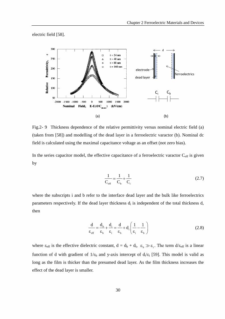
The dependence of dielectric constant on film thickness is observed by many groups [58-60].
The measured dielectric constant decreases significantly with the thickness as shown in Fig.2-
9 (a) [58]. The decrease in dielectric constant can be effectively modelled by assuming the
presence of a “dead layer” at the electrode/ferroelectric interface. The dead layer is considered
as a thin dielectric layer with severely depressed dielectric constant and tunability. The dead
layer is modelled as in series with the bulk like ferroelectrics as shown in Fig.2- 9 (b) so the
decrease in dielectric constant follows the “series capacitor model” [59]. It is also observed
from Fig.2- 9 (a) that the dielectric constant becomes less dependent on thickness at higher
Chapter 2 Ferroelectric Materials and Devices
30
electric field [58].
d
di
dead layer
Ci Cb
ferroelectrics
(a) (b)
electrode
Fig.2- 9 Thickness dependence of the relative permittivity versus nominal electric field (a)
(taken from [58]) and modelling of the dead layer in a ferroelectric varactor (b). Nominal dc
field is calculated using the maximal capacitance voltage as an offset (not zero bias).
In the series capacitor model, the effective capacitance of a ferroelectric varactor Ceff is given
by
eff b i
1 1 1C C C
= + (2.7)
where the subscripts i and b refer to the interface dead layer and the bulk like ferroelectrics
parameters respectively. If the dead layer thickness di is independent of the total thickness d,
then
b ii
eff b i b i b
d dd d 1 1d
= + = + − ε ε ε ε ε ε (2.8)
where εeff is the effective dielectric constant, d = db + di, b iε ε . The term d/εeff is a linear
function of d with gradient of 1/εb and y-axis intercept of di/εi [59]. This model is valid as
long as the film is thicker than the presumed dead layer. As the film thickness increases the
effect of the dead layer is smaller.
Chapter 2 Ferroelectric Materials and Devices
31
One problem that impedes the microwave applications of ferroelectrics is the temperature
dependence of the dielectric constant. The dependence is especially strong for temperatures
close to the phase transition temperature. One possible solution for this problem is
incorporating a temperature stabilisation bias network [15]. The bias network consists of a
voltage divider (a fixed capacitor in series with temperature sensitive capacitor usually using
similar ferroelectrics) and a DC decoupling network. The capacitance changing with
temperature can be compensated by the changing of the distributed voltage. However, this
temperature stabilisation is obtained at the cost of requiring a higher tuning voltage.
Lifetime and reliability are also crucial issues in practical applications of ferroelectric devices.
The most important failure mechanism is resistance degradation, which is characterised by a
steady but pronounced increase of leakage current under a constant DC bias after a specific
time. Detailed analysis and models of resistance degradation and other reliability issues can
be found in [61].
In summary, the quality and dielectric property of BST thin films are complex functions of
electric field, temperature, frequency, composition and film thickness. In addition, they also
depend on the processing, e.g. deposition method, growth conditions, defect density, substrate
and metallisation choices. A good understanding of these relationships is essential prior to the
microwave applications of ferroelectrics becoming commercial.
2.3 BST deposition methods
There are various ways to grow BST films and each one has its merits and drawbacks. The
method of choice is usually determined by the application, system requirement and cost.
Generally, the deposition methods can be divided into three main categories, which are (i)
physical vapor deposition (PVD) including electron beam evaporation, magnetron sputtering
and pulsed laser deposition (PLD); (ii) chemical vapor deposition (CVD) including metallic
organic CVD (MOCVD) and atomic layer deposition (ALD); (iii) chemical solution
deposition (CSD) like sol-gel. The most popular deposition methods for BST thin films such
as sol-gel, MOCVD, magnetron sputtering and PLD will be discussed as follows.
The Sol-gel process offers the advantages of low cost, good composition control and it does
Chapter 2 Ferroelectric Materials and Devices
32
not require vacuum infrastructure. The precursor solution with the right concentration of
cations should be prepared and deposited on the substrate by spin-coating, and this is repeated
to reach the desired thickness. Then a low temperature heat treatment (300 - 400 °C) is
performed to dehydrate the organic species and form an amorphous film. Finally, high
temperature heat treatment (600 - 1100 °C) for densification and crystallization of the film is
performed. The Sol-gel process has been investigated for preparation of high quality
ferroelectric materials by many research groups [62-65]. A phase shifter made with a sol-gel
BST thin film deposited on LAO is demonstrated in [66]. It has a 40.9 °/ dB figure of merit at
14.2 GHz, which is comparable to the BST thin film phase shifter of the same design grown
using the PLD process.
Metal organic chemical vapor deposition (MOCVD) is a technique to grow epitaxial films on
a substrate surface based on chemical reaction of metal organic gaseous precursors at high
temperature. MOCVD offers the potential for large scale deposition, good composition
control, highly uniform and highly conformal films on planar and high aspect ratio substrates
[67], [68]. However, MOCVD process is limited by the availability of suitable precursors and
process control difficulties [69]. A parallel plate capacitor with 71 % tuning at 9 V (which is
30 V/µm electric field) was reported using a Ba0.7Sr0.3TiO3 film deposited by MOCVD
technique [70]. The loss tangent of the film was in the range of 0.003 - 0.009 up to 500 MHz.
Magnetron sputtering is a versatile technique which can deposit conductive and insulating
thin films onto metal or ceramic substrates. It is a vacuum process which physically removes
portions of target material and deposits a thin layer onto the substrate surface. Sputtering can
be either DC or RF depending on the nature of the target. DC power is used when the target is
conducting, while RF can be used for both conducting and insulating targets. The principle of
DC sputtering is shown in Fig.2- 10. The chamber is filled with argon gas at low pressure.
When the target is connected to a negative high voltage, a glowing plasma forms just above
the target surface, the plasma consists of electrons and positive argon ions in a high energy
state. The ions are accelerated towards the negatively charged target and strike it. This causes
the atoms of the target material to be ejected, and some of the atoms land on and bond with
the substrate which is mounted in front of the target, building a thin film. The word
“magnetron” refers to placing of a magnet behind the target, resulting a very high density of
ions, which in turn increases the sputtering rate. At Birmingham, metal films of several
Chapter 2 Ferroelectric Materials and Devices
33
hundred nanometres thick were deposited using the DC and RF magnetron sputtering system
shown in Fig.2- 11.
Oxide materials such as BST can be only successfully grown by sputtering when the reactive
sputtering technique is used. In reactive sputtering, a gas (e.g. O2) is added to the argon
introduced into the sputtering system. The quality and properties of BST thin films deposited
by reactive sputtering depends on the substrate temperature, power and composition of target,
pressure, ratio of partial pressure of Ar and O2 [69].
The pulsed laser deposition (PLD) technique has been widely used to grow high quality
ferroelectric films for microwave application. As shown in Fig.2- 12, a high power pulsed
laser beam is focused on a spot of the target surface to strike the target. The high energy
density vaporises the target material and a plume of material is transported towards and
deposited on the heated substrate facing the target. This process can occur in vacuum or in the
presence of a reactive background gas, such as oxygen, which is commonly used in oxide
deposition to fully oxygenate the deposited films, as in reactive sputtering. The background
gas pressure, the substrate to target distance, laser energy and frequency, and substrate
temperature have important effects on the BST thin film composition, microstructure and
properties. To produce high quality BST thin films for microwave applications, intensive
research effort has been made to clarify the correlation between the deposition conditions and
film properties, and to optimise the growth conditions [71-73]. Compared with vacuum
evaporation and sputtering, PLD has a higher maximum deposition rate although slowing
down of the deposition rate from the maximum is often required to obtain high quality films.
The deposition temperature is relatively low as a result of high ionic content in laser plumes
and high particle velocity [71]. PLD is appropriate for deposition of complex oxide materials
as a result of stoichiometric transfer of the complex materials to thin films [74]. The PLD
process is also best suited to deposition on small (1 cm2) substrate. Deposition over large
areas is possible but technically challenging. So for commercial processes or larger area
devices the previously discussed deposition processes are more suitable. One major drawback
PLD process suffers is the formation of droplet or particulate production due to the melting or
fracture of the target surface. This problem may be tackled by a careful control of the laser
energy just above the ablation threshold [71]. All the BST thin films used in this work were
deposited by PLD process. A photo of the PLD system at Birmingham is shown in Fig.2- 13.
Chapter 2 Ferroelectric Materials and Devices
34
Fig.2- 10 Principle of DC magnetron sputtering (taken from [75])
Fig.2- 11 DC and RF magnetron sputtering equipment at Birmingham
Chapter 2 Ferroelectric Materials and Devices
35
Fig.2- 12 Schematic of PLD deposition chamber (taken from [76])
Fig.2- 13 Pulsed laser deposition chamber at Birmingham
Chapter 2 Ferroelectric Materials and Devices
36
2.4 Microwave characterisation techniques of ferroelectric thin
films
The properties (real and imaginary parts of permittivity and tunability) of ferroelectric thin
films at microwave frequencies can be extracted by several methods, characterised as varactor
methods, transmission line methods and resonance methods. At microwave frequencies,
usually the devices cannot be modelled as lumped elements due to the presence of various
parasitic effects, hence distributed models are often required. A good calibration prior to the
measurement is also essential for accurate extraction of the dielectric properties of
ferroelectric thin films.
In the resonance method, where a transmission line resonator is patterned on the BST thin
film [77] or interrupted by a BST gap capacitor [78], the permittivity and loss tangent of the
BST thin film are calculated from the measured resonant frequency and unloaded quality
factor. This method can give a precise extraction of the loss tangent especially for low loss
material [48]. However, the resonance method can only give information at one frequency
point and the frequency dependent dielectric properties of the BST thin film are not available.
Parallel plate or planar varactors are commonly used structures to characterise the dielectric
properties of BST thin film as functions of frequency and electric field. One port reflection
data or two port S-parameters are often measured using a vector network analyser. The
extraction of dielectric properties of BST film is complicated at microwave frequencies
because the loss from electrodes and lead strips is also important and parasitic inductance and
capacitance will affect the apparent capacitance. The parasitic and peripheral circuit effect can
be removed either by additional structures [79], [80] or by evaluation of electric models [49],
[81], [82].
Chapter 2 Ferroelectric Materials and Devices
37
Fig.2- 14 capacitor (a), through line 1 (b), and through line 2 (c) (taken from [79])
(a)
(b)
(c)
(d)
Fig.2- 15 Top view (a), cross sectional view (b), physics based equivalent circuit (c) and its
representation circuit (d) of a circular parallel plate varactor (taken from [81])
For a parallel plate capacitor, an electrode size as small as several microns is often required as
a result of the high dielectric constant of ferroelectrics and small film thickness. Otherwise, a
large capacitance will lead to an equivalent short circuit at microwave frequency. A simple
two port measurement technique has been reported in reference [79]. The BST parallel plate
capacitor was embedded in a transmission line and two “through lines” were used to
Chapter 2 Ferroelectric Materials and Devices
38
de-embed the effect of the transmission line as shown in Fig.2- 14. The capacitance and loss
tangent were extracted from the measured responses for up to 12 GHz. The extracted
capacitance showed little dispersion with frequency and a tunability of 2.4 was achieved at 15
V. The extracted loss tangent was less than 0.012 up to 10 GHz.
For a relatively simple structure, circuit modelling methods can be used to remove the
parasitic inductance and series resistance in the test structure. An example of using a circuit
model to characterise the BST thin film in a circular parallel plate capacitor was given by
Vorobiev [81]. The capacitor had a simple layout as shown in Fig.2- 15 (a) and (b) and its
circuit model and simplified model were shown in Fig.2- 15 (c) and (d). The test structure
offered minimised losses and parasitic inductance from the electrodes which helped to
determine the loss from BST thin film. The large capacitance between the outer circular top
plate and the bottom plate was equivalent to a short circuit in the microwave region and
allowed a DC bias to be applied. The parasitic inductance and negative calibration inductance
was removed. The extracted capacitance showed little dispersion up to 25 GHz. The loss of
the BST thin film was separated from the electrode loss and the BST loss tangent was
reported to be around 0.02 up to 25 GHz.
The extraction of dielectric properties in the microwave region using interdigital capacitor
(IDC) structures is more difficult because of the presence of various parasitic effects.
Conformal mapping based models are often used to extract the permittivity [83]. Knowledge
of the geometry of interdigital fingers, the thickness of the BST thin film and substrate, and
the permittivity of the substrate is required to calculate the dielectric constant of BST film.
The permittivity can also be determined by comparing the experimental results with a set of
full wave electromagnetic simulation results [84].
Transmission line structures, particularly the coplanar waveguide (CPW), can be also used to
determine the properties of BST thin film. The impedance of the transmission line should be
close to 50 Ω to reduce the signal reflection. The transmission line can be modelled using full
wave simulation, or, it can be analysed using an equivalent circuit model [77]. The
propagation constant γ (γ = α + іβ where α is the attenuation constant and β is the phase
constant) and the line impedance Z0 are determined from the ABCD-parameters calculated
from the measured S-parameters. The permittivity of BST thin film is calculated from the
Chapter 2 Ferroelectric Materials and Devices
39
effective permittivity using the conformal mapping method.
It should be noted that the characterisation methods discussed above are not complete but
emphasis is placed on BST thin films in the microwave region. Examples of simple
characterisation methods based on BST parallel plate capacitors are given. More detailed
discussions and comparisons of different extraction methods can be found in [29], [41], [48],
[77].
2.5 Substrate choice
BST thin films have been deposited on oxide single crystal substrate such as sapphire (Al2O3)
Fig.2- 16 Skin depth of several common metals versus frequency
Chapter 2 Ferroelectric Materials and Devices
43
Pt [70], [102], Ir [103], Ru [103], Cu [97], Au [92] and SrRuO3 [104] are the electrodes that
have been tried as bottom electrode of BST devices. Pt is the most popular bottom electrode
material because of its stability against oxidisation and relatively high conductivity compared
with oxide electrodes [48]. Pt also has a lattice parameter (a = 0.3924 nm) close to that of BST
with 25 % Ba concentration and initiates quasi-epitaxial growth of BST film [9]. In addition,
the high work function of Pt (5.65 eV) results in a low leakage current [80]. However, careful
treatment is required during the deposition, annealing and cooling process. The difference in
CTE between Pt and the substrate can cause strain at the electrode/substrate interface and
roughen the electrode. A slow cooling procedure can help to resolve this problem [48].
Another problem is that the step near the edge of the patterned bottom electrode may cause a
short circuit in the parallel plate structure [48]. Thicker BST films or a ramp at the electrode
edge can help to prevent such problems. In addition, beneath the Pt layer, a thin adhesion layer
such as Ti, TiO2, Cr, SiO2 and IrO2 is often used to enhance adhesion to substrate. In the case of
devices on silicon substrate, a thin SiO2 layer is often used as a barrier against oxygen
diffusion.
The thickness of the Pt bottom electrode is usually in the range of 50 - 200 nm which is much
smaller than its skin depth in gigahertz range. This inevitably leads to high current
concentration in the electrode and inferior the total loss performance of the device. One
possible solution is to deposit a thicker gold layer between two platinum layers as both larger
thickness and better conductivity result in lower loss [51].
2.7 Ferroelectric varactors
(a) (b)
BST film
Interdigital electrodesTop electrode
Substrate Bottom electrode
Fig.2- 17 Schematics of a BST interdigital (a) and parallel plate (b) capacitor
Chapter 2 Ferroelectric Materials and Devices
44
Ferroelectric varactors are the core elements of ferroelectric tunable filters, phase shifters and
tunable matching networks. Interdigital and parallel plate are two common configurations of
ferroelectric varactors, both utilizing the property that the dielectric constant of the BST thin
film can be altered by applying a DC voltage, thus tuning the capacitance. The schematic
layouts of the two types of varactors are shown in Fig.2- 17.
Interdigital capacitors (IDCs) have a simple fabrication process because only single step
photolithography is required. The BST thin film is deposited directly on the substrate and the
top metal layer is then defined on the film surface. A capacitance range of 0.1 - 10 pF can be
obtained by simply changing the number of fingers, the length of fingers and the gap between
the fingers. However, IDCs typically require a bias voltage as high as 40 - 400 V depending of
the space between the fingers. The tunability of interdigital capacitor is usually smaller than
that in the parallel plate configuration for a given bias voltage because part of the electric field
is in air thus is not effectively tuned and the electrodes of IDC are at least a factor of 10 further
apart than that of the parallel plate capacitor. In addition, it is difficult to extract the material
properties directly and empirical formula and full wave electromagnetic simulation are often
required.
Although the IDC is popular due to its relatively simple fabrication, the high bias voltage
requirement impedes the application of IDC in all but specific systems. In practical applications,
the parallel plate capacitor is more attractive because it is compact and requires a low bias
voltage. BST parallel plate capacitors have a very high energy density as a result of the high
dielectric constant of the BST thin film. A capacitance of 1 pF can be comprised of an parallel
plate area of 25 - 100 µm2 corresponding to a capacitance density of 40 -10 fF/µm2. The tuning
voltage for a parallel plate capacitor is usually below 30 V, which is much smaller than that of
interdigital ones. For example, a bandpass filter using BST parallel plate capacitors shows
57 % tuning of the centre frequency with the application of 6 V bias [100]. The low bias
voltage not only eliminates the need for a DC transformer but also provides possibility to
integrate with semiconductor technologies. However, the processing of BST parallel plate
capacitors is more complicated. In the parallel plate configuration, the BST thin film is typically
grown on metallised substrate with adhesion layers. One key problem in the multilayer
structure is the difference in thermal expansion coefficient and lattice parameter of different
layer, as discussed in previous section. This difference can lead to substantial misfit strain on
Chapter 2 Ferroelectric Materials and Devices
45
the BST/electrode or electrode/substrate interface and can roughen or cause hillocks in the
BST film or electrodes [48]. In addition, two or more steps of photolithography are required to
define the top and bottom electrodes and micron-level lithography is often required for
capacitances less than 1 pF. These fabrication issues make the production of high Q varactor
challenging.
Despite the fabrication difficulties, BST IDC with a Q of 30 at 20 GHz [67] and BST parallel
plate capacitor with a Q of 50 at 40 GHz [51] have been reported. These values are
comparable or better than semiconductor analogs at the same frequency range. Tunability and
Q are often tradeoffs in BST varactor design. The optimal tradeoff between the tunability and
Q can be characterised by the commutation quality factor defined in equation (2.6) [27].
RF power handling capability, which is the ability to transmit high microwave power levels
without unacceptable degradation of signals due to intermodulation distortion, is another
important feature of tunable devices. The amount of intermodulation distortion (IMD) is
related to the DC bias voltage required as follows [99]
RF
DC
VIMDV
∝ (2.11)
where VRF is the amplitude of the RF signal and VDC is bias voltage required for tuning. High
power handling capability can be achieved at a cost of higher tuning voltage. For example,
interdigital capacitors typically have higher power handling capability and better linearity
than parallel plate capacitors [67]. Optimal tradeoff between power handling and DC bias
required (or tunability) can be made by simply adjusting the gap between fingers in the
interdigital configuration. A ferroelectric gap capacitor with improved IMD and simultaneous
high tunability at low bias voltage was presented in [52]. Separate high resistance DC bias
electrodes were fabricated in the gap to enhance the DC electric field. The IMD performance
of the gap capacitor with this bias structure was improved by 6 dB over a conventional
structure with the same tunability.
The substrate material, BST composition and deposition method, electric field, tunability, Q
and CQF of several published BST capacitors in both interdigital and parallel plate
configuration are summarised in Table 2- 2. The BST capacitor made in this work (discussed
Chapter 2 Ferroelectric Materials and Devices
46
in appendix A) is also included in Table 2- 2, having a CQF of 235 at 2 GHz, which is
comparable to or better than other published results. It should be noted that the CQF of a
ferroelectric varactor depends on both the electric field and operating frequency. A higher
electric field leads to higher tunability thus higher CQF. Q will be considerably degraded in
the high gigahertz region and so will the CQF.
Reference Capacitor
configuration /Substrate
Ba/Sr ratio /Deposition
method
Bias(V)/ Electric
field(V/µm)
Capacitance (pF) Permittivity Relative
tunability Q CQF
Kirchoefer et al. 1998
[53]
interdigital /LaAlO3
50:50 PLD
0~40 0~8 3.4~1.0 2700~700 70.6% 13~17 374.4
at 2 GHz Nash
et al. 2005 [105]
interdigital /Sapphire
25:75 magnetron sputtering
0~35 0~7 0.63~0.55 NA 21% 100~250 461.8
at 1 MHz Ouaddari et al. 2005
[49]
interdigital /Alumina
50:50 PLD
0~35 0~4.4 NA 620~520 15% 14.3 5.4
at 6 GHz Kenney
et al. 2006 [106]
interdigital /Sapphire
57:43 CCVD2
0~80 0~40 NA NA 61% 74~27 1906
at 2.4 GHz Vendik
et al. 2003 [107]
Microstrip gap/Alumina NA 0~150
0~15 0.35~0.19 NA 45.7% 22.7~58.8 514.7
at 4 GHz Marsan
et al. 2005 [102]
Parallel plate /Alumina
50:50 PLD
0~19 0~34 2.9~0.9 NA 71% 14~13 309
at 1 GHz Tombak
et al. 2002 [70]
Parallel plate /Silicon
70:30 MOCVD
0~9 0~130 65.0~19.2 200~60 71% 20 677.6
at 300 MHz Vorobiev
et al. 2003 [51]
Parallel plate /HR silicon
25:75 PLD
0~25 0~83.3 2.2~1.4 150~75 40% 180~240 8977
at 1MHZ
this work Parallel plate /HR silicon
25:75 PLD
0~13 0~32.5 1.63~1.14 738~514 30% 45.5~40.0 235
at 2GHz
Table 2- 2 A comparison between several published BST varactors and the BST varactor made
in this work.
2 CCVD stands for combustion chemical vapor-phase deposition.
Chapter 2 Ferroelectric Materials and Devices
47
2.8 Ferroelectric tunable filters
Various ferroelectric thin film (BST or STO) tunable filters have been reported by several
research groups and companies. These filters can be classified as many different types: they
are based on a lumped element or distributed line approach or a combination; they are
implemented in a coplanar waveguide or a microstrip configuration; they have single or multi
metal layer structure; and they use ferroelectric varactors in integrated or discrete form.
For a tunable filter, the tuning range, bandwidth and filter insertion loss are the important
parameters describing the filter performance. These parameters can be characterised as the
figure of merit (FoM) and different tunable filters can be compared in terms of FoM. The
FoM of a tunable filter is defined as [108]
12 1
1 2 1 2
1F dBIL IL
−ω −ω=
∆ω ∆ω (2.12)
where ω1, ω2 are the centre frequency of two states, Δω1, Δω2 are the bandwidth and IL1, IL2
are the insertion loss at the pass band in two states. The FoM of some reported BST filters
will be given in Table 2- 3 and the FoM of our BST filters will be given in chapter 6. The
maximum available FoM of a tunable filter based on ferroelectric varactors is related to the
filter order N and the commutation quality factor K of the ferroelectric capacitor and is
determined as [109]
11F K dB8.68N
−= (2.13)
The FoM is electric field dependent. At higher electric field, the tunability is larger and so is
the FoM. FoM is also frequency dependent. At higher frequency, the loss from both BST and
metal is increased and leads to a lower FoM. When comparing FoM of different filters, the
operating frequency and electric field must be taken into account.
Keis [110] reported a 20 GHz tunable filter using a BST thick film (5 mm thick) gap
capacitors on a MgO substrate. The filter was based on a symmetrical fin-line topology in a
rectangular waveguide. The width and length of the capacitor gap was 0.05 mm and 0.5 mm
Chapter 2 Ferroelectric Materials and Devices
48
respectively, which gave a capacitance of 0.4 pF at zero bias, tuned to 0.15 pF with 400 V bias
(which is 8 V/µm electric field), at 20 GHz. The centre frequency could be tuned 1.8 GHz
(which is 9 %) from 20 GHz with a 3.5 % 3dB fractional bandwidth. The filter had an
insertion loss better than 3.5 dB and reflection loss better than 20 dB in the tuning range. This
was one of the first reported BST thick film tunable filters at room temperature.
Pleskachev [109] reported tunable microstrip filters using ferroelectric thin film capacitors.
The filters were based on short circuit or open circuit resonators with BST or STO thin films
on an alumina substrate. The ferroelectric capacitors were formed by 10 µm wide gaps in the
microstrip lines. 4 µm thick copper metallisation was used. The 3-pole bandpass filter based
on a short circuit resonator and BST gap capacitors was measured at room temperature. The
centre frequency tuned from 4.4 GHz to 4.7 GHz at 150 V (which is 15 V/µm electric field),
with a 15 - 8 dB insertion loss at passband. The figure of merit of the measured filter was 0.34
dB-1. The 2-pole bandpass filter based on open circuit resonator and STO film was measured
at 77 K. The figure of merit was 0.17 dB-1.
Tan [38] reported a planar tunable HTS filter with a patterned Ba0.1Sr0.9TiO3 thin film on a
LaAlO3 substrate. The YBCO thin film was first patterned to form a negative image for BST
thin film deposition. After the BST film deposition, the remaining YBCO and unwanted BST
film were removed, leaving the BST thin film with desired pattern. A YBCO conducting layer
was then deposited and patterned using conventional photolithography and wet etching. The
3-pole microstrip filter was comprised of open loop resonators with BST gap capacitors
between the two ends. At 77 K, the filter was measured to have a centre frequency of 11.74
GHz when in the unbiased state and the centre frequency increased to 11.93 GHz (tuned
1.6 %) under 200 V (which corresponds to an electric field of 2 V/µm). The insertion loss of
the filter was 1.6 dB at zero bias and 0.35 dB at 200 V. The low insertion loss demonstrated
the potential of achieving low loss microwave tunable devices using ferroelectric materials.
The filter had a figure of merit of 0.51 dB-1.
Subramanyam [111] presented a novel ferroelectric varactor shunt switch in coplanar
waveguide configuration on a high resistivity silicon substrate. The switch consisted of a
CPW line loaded by a shunt varactor. The ferroelectric varactor had the highest capacitance at
zero bias, resulting in signals shunted to the ground and the output port isolated from the input
Chapter 2 Ferroelectric Materials and Devices
49
port (i.e. off-state). Applying a bias voltage drove the capacitance of the varactor to its lowest
value and allowed signals to pass through from the input to output ports (on-state). The
capacitor area was 5 × 15 µm2. The switch had an isolation (difference in insertion loss of
on-state and off-state) of 16.6 dB at 45 GHz and the on-state insertion loss is 7.1 dB at 9.5 V
bias (which corresponds to an electric field of 23.75 V/µm). The switching speed of the
varactor shunt switch was tested. The rise and fall times for the device were estimated to be
approximately 43 ns.
Tombak [100] reported third order and fifth order lumped element lowpass filters. The filters
consisted of BST parallel plate capacitors and coil inductors connected by bond wires. The
quality factor of a 65 pF BST varactor was 63 at 45 MHz, which was comparable to the
commercially available varactor diode of similar capacitance and frequency. The third order
lowpass filter had an insertion loss of 0.8 dB and the 3 dB cut-off frequency was tuned 30 %
from 120 to 170 MHz with 0 - 9 V DC bias (which is 30 V/µm electric field). The reflection
was better than 10 dB for all biasing conditions. The fifth order lowpass filter had about 2 dB
insertion loss and a return loss better than 7 dB with a 40 % tunability by application of 0 - 9
V bias. The IP3 point of the third order and fifth order filter was 24 dBm and 22 dBm at 0 V
respectively. A similar tunable bandpass filter was reported as well and the results are
included in the summary in Table 2- 3.
Various BST bandpass filters at room temperature have been reported recently and some of
the best results are summarised in Table 2- 3 in terms of electric field required, centre
frequency, bandwidth, tunability, passband insertion loss and reflection, and figure of merit.
Interdigital or parallel plate capacitors are used in integrated or discrete manner.
Intermodulation distortion (IMD) is compared as well in terms of the IP3 points. Filters using
interdigital capacitors exhibit higher IP3 than those using parallel plate capacitors. This is in
large part because the interdigital configuration enables RF field to spread over large volumes
[99]. The electrode gap is typically 3 - 20 µm and length of finger 0.1 - 0.4 mm, whereas the
dimensions of parallel plate capacitors are of the order of microns. Another reason is that IMD
is inversely related to DC bias voltage as shown in equation (2.11). Interdigital capacitors
which require higher bias result in lower IMD compared with parallel plate capacitors.
It should be noted that filters using discrete BST varactors have lower insertion loss. At
Chapter 2 Ferroelectric Materials and Devices
50
microwave frequencies, the metal loss becomes pronounced in ferroelectric thin film devices
as a result of the small metal thickness. The filters using discrete BST varactors usually have
much thicker transmission lines and the metal loss is considerably reduced. Discrete BST
varactors are assembled on the circuit using silver epoxy or bond wires.
A tunable bandpass filter using discrete BST varactors demonstrated in this work is also
included in Table 2- 3. It has a FoM of 0.87 dB-1 at an electric field of 6.5 V/µm, which is
much higher than other published filters.
Reference Capacitor
configuration/ Integration
Bias voltage
(V)/ Electric
field (V/µm)
Centre frequency
(GHz)/ Tunablility
Band width
(before bias)
Insertion loss(dB)/ minimum
return loss (dB)
IP3 (dBm)
Top metal/ Filter order
FoM (dB-1)
Tombak, et al. 2003[100]
parallel plate/ discrete
0~6/ 0~20
0.176~0.276/ 56.8% 40% 3/
7 19 Pt/ 3 0.35
Pleskachev, et al. 2004[109]
gap/ integrated
0~150/ 0~15
4.40~4.65/ 5.7% 3% 15~8/
NA NA Cu/ 3 0.34
Kuylenstierna, et al. 2006[112]
parallel plate/ integrated
0~13/ 0~43.3
40~50/ 25 % 25% 9.5~9.0/
4.5 NA Au/Pt/ 1 0.097
Papapolymerou, et al. 2006[113]
planar/ integrated
0~30/ NA
11.5~14/ 22% 14% 5.4~3.3/
10 31 Cu/Pt/ 2 0.322
Subramanyam, et al. 2001[114]
gap/ integrated
0~100/ 0~4
16.69~17.17/ 3% 2% 8.1~5.3/
NA NA Au/ 2 0.22
Lugo, et al. 2007[115]
planar/ integrated
1~40/ NA
34.0~37.5/ 10.3% 9.6% 9.0~2.7/
4 NA Ti/Au/Pt/ 2 0.207
Nath, et al. 2005[105]
interdigital/ integrated
0~200/ 0~40
2.44~2.88/ 18% 24.6% 5.1~3.3/
13 41 Cu/ 3 0.155
Nath, et al. 2006[98]
interdigital/ discrete
0~130/ 43.3
2.14~2.61/ 22% 18% 4.9~2.9/
11 32 Cu/ 2 0.292
this work interdigital/ discrete
0~65/ 0~6.5
1.55~2.02/ 30.3% 15.5% 3.7~1.1/
15 NA Ag/ 2 0.87
Table 2- 3 A comparison of published BST thin film bandpass filters at room temperature
Chapter 2 Ferroelectric Materials and Devices
51
2.9 Other ferroelectric devices
The phase shifter is one of the simplest microwave components using ferroelectrics. A
continuously variable phase shifter is the most critical component of phased array antennas.
Phase shifters can be implemented in different ways, such as a switched line phase shifter, a
lowpass/highpass phase shifter, a reflection type or a loaded line phase shifter. The first two
types typically use switches whereas the latter two can produce continuous phase tuning using
variable capacitors. The most desirable features of a phase shifter are large phase shift ΔΦ and
low insertion loss. Subsequently, the figure of merit of a phase shifter is defined as the phase
shift divided by loss
dB
FoMIL∆Φ
= (2.14).
FoM is related to the commutation quality factor K of the loaded varactor as follows [116]
FoM 6.6 K= (2.15).
Coplanar waveguide transmission lines on top of Ba0.5Sr0.5TiO3 thin film/MgO substrate were
made at Birmingham and functioned as phase shifters [117]. The correlation between the
microwave performance of the device and the operating temperature, the microstructure of
BST thin film were investigated. A FoM of 12.5 °/dB was obtained with optimised grown
conditions. Acikel [118] reported a phase shifter comprised of a CPW line periodically loaded
with ST parallel plate capacitors. The circuit provided 240° of phase shift with an insertion
loss of 3 dB at 10 GHz under 17.5 V DC bias. A figure of merit of 93 °/dB was achieved at
6.3 GHz, which is the best reported figure of merit for a BST phase shifter.
In addition, voltage controlled oscillators [119], tunable matching networks [120] and delay
lines [121] utilizing the electric field dependent dielectric constant of ferroelectric materials
have been also reported by many research groups.
Chapter 2 Ferroelectric Materials and Devices
52
2.10 Summary
The fundamentals of ferroelectric thin films were presented in this chapter and fabrication
issues such as deposition methods, choice of substrate and metallisation were discussed.
Understanding of these fundamentals was essential for the designing and optimising of
ferroelectric tunable devices. Published results of ferroelectric varactors and tunable filters
were reviewed and compared in detail. In addition, recent progress on BST thin film varactors
for room temperature microwave applications is reviewed [48]. In the next chapter models of
the coplanar waveguide transmission line will be presented and the general microwave filter
synthesis procedure will be introduced.
Chapter 2 Ferroelectric Materials and Devices
53
References
[1] Y. Xu, Ferroelectric Materials and Their Applications, North-Holland, 1991. [2] W.D.Kingery, H.K.Bowen, and D.R.Uhlman, Introduction to Ceramics. New York,
USA, John Wiley and Sons, 1960. [3] J. Valasek, "Piezo-Electric and Allied Phenomena in Rochelle Salt", Physical Review,
vol. 17, no. 4, pp. 475-481, 1921. [4] A. V. Hippel, R.G.Breckenridge, F.G.Chesley, and L. Tisza, "High dielectric constant
ceramics", Industrial and Engineering Chemistry, vol. 38, no. 11, pp. 1097-1109, 1946.
[5] B.Wul and J.M.Goldman, C.R.Acad.Sci.URSS, vol. 51, no. p. 21, 1946. [6] "Complex perovskite-type oxides", in Landoldt-Bornstein: oxides. vol. 28,
K.H.Hellwege and A.M.Hellwege, Eds. Springer-Verlag, 1990. [7] D. Czekaj, E. Jaszczyszyn, T. Orkisz, L. Kozielski, Lisiiiska-Czekaj, E. Federowicz,
and J. Modelski, "Synthesis and Basic Properties of Ferroelectric Thin Films. Methods Materials and Novel Applications", in International Conference on Microwaves, Radar & Wireless Communications2006, pp. 692-699.
[9] P. Rundqvist, "(Ba,Sr)TiO3 ferroelectric thin films for microwave applications", Doctor of Philosophy thesis, Department of Microtechnology and Nanoscience, Chalmers University of Technology, 2006
[10] S. Zubko, "Ferroelectrics:Physics and microwave applications", Visiting seminar, no. 2007.
[11] C.A.Randall, R.E.Newnham, and L.E.Cross, "History of the first ferroelectric oxide, BaTiO3", Materials Research Institute, The Pennsylvania State University.
[12] M. Daglish and T. Kemmitt, "Ferroelectric thin films - research, development and commercialisation", IPENZ Transactions, vol. 27, no. pp. 21-24, 2000.
[13] D. W. Chapman, "Some Thin-Film Properties of a New Ferroelectric Composition", Journal of Applied Physics, vol. 40, no. 6, pp. 2381-2385, 1969.
[14] M. H. Francombe, "The Research Status and Device Potential of Ferroelectric Thin Films", IEEE Transactions on Sonics and Ultrasonics, vol. 19, no. 2, pp. 199-212, 1972.
[15] N. Setter, D. Damjanovic, L. Eng, G. Fox, S. Gevorgian, S. Hong, A. Kingon, H. Kohlstedt, N. Y. Park, G. B. Stephenson, I. Stolitchnov, A. K. Taganstev, D. V. Taylor, T. Yamada, and S. Streiffer, "Ferroelectric thin films: Review of materials, properties, and applications", Journal of Applied Physics, vol. 100, no. 10, p. 109901, 2006.
[16] J.B.Blum and S.R.Gurkovich, "Sol-gel-derived PbTiO3", Journal of Materials Science, vol. 20, no. pp. 4479-4483, 1985.
[17] K.D.Budd, S.K.Dey, and D.A.Payne, "Sol-gel processing of lead titanate (PbTiO3), lead zirconate (PbZrO3), PZT, and PLZT thin films", British Ceramic Proceedings, vol. 36, no. p. 107, 1985.
[18] S. Baik, N. Setter, and O. Auciello, "Preface: Science of ferroelectric thin films and application to devices", Journal of Applied Physics, vol. 100, no. p. 051501, 2006.
[19] R. W. Whatmore, Q. Zhang, Z. Huang, and R. A. Dorey, "Ferroelectric thin and thick films for microsystems", Materials Science in Semiconductor Processing, vol. 5, no.
Chapter 2 Ferroelectric Materials and Devices
54
2-3, pp. 65-76, 2002. [20] Y. Nemirovsky, A. Nemirovsky, P. Muralt, and N. Setter, "Design of novel thin-film
piezoelectric accelerometer", Sensors and Actuators A: Physical, vol. 56, no. 3, pp. 239-249, 1996.
[21] M. A. Dubois and P. Muralt, "PZT thin film actuated elastic fin micromotor", IEEE Transactions on Ultrasonics, Ferroelectrics and Frequency Control, vol. 45, no. 5, pp. 1169-1177, 1998.
[22] P. Muralt and J. Baborowski, "Micromachined Ultrasonic Transducers and Acoustic Sensors Based on Piezoelectric Thin Films", journal of electroceramics, vol. 12, no. 1, pp. 101-108, 2004.
[23] F. Toru and W. Shunji, "Feedback positioning cantilever using lead zirconate titanate thin film for force microscopy observation of micropattern", Applied Physics Letters, vol. 68, no. 4, pp. 467-468, 1996.
[24] M. J. Kenneth, "Variation of Dielectric Constant with Voltage in Ferroelectrics and Its Application to Parametric Devices", Journal of Applied Physics, vol. 33, no. 9, pp. 2826-2831, 1962.
[25] M. DiDomenico, D. A. Johnson, and R. H. Pantell, "Ferroelectric Harmonic Generator and the Large-Signal Microwave Characteristics of a Ferroelectric Ceramic", Journal of Applied Physics, vol. 33, no. 5, pp. 1697-1706, 1962.
[26] D. Dimos and C. H. Mueller, "Perovskite thin films for high-frequency capacitor applications", Annual Review of Materials Science, vol. 28, no. 1, pp. 397-419, 1998.
[27] O. G. Vendik, E.K.Hollmann, A. B. Kozyrev, and A. M. Prudan, "Ferroelectric tuning of planar and bulk microwave devices", Journal of Superconductivity, vol. 12, no. pp. 325-338, 1999.
[28] G. David, C. P. John, A. B. James, and H. O. Ronald, "Characterization of a tunable thin film microwave YBa2Cu3O7-x/SrTiO3 coplanar capacitor", Applied Physics Letters, vol. 63, no. 22, pp. 3078-3080, 1993.
[29] A.K.Tagantsev, V.O.Sherman, K.F.Astafiev, J.Venkatesh, and N.Setter, "Ferroelectric materials for microwave tunable applications", Journal of Electroceramics, vol. 11, no. pp. 5-66, 2003.
[30] D. Galt, J. C. Price, J. A. Beall, and T. E. Harvey, "Ferroelectric thin film characterization using superconducting microstrip resonators", IEEE Transactions on Applied Superconductivity, vol. 5, no. 2, pp. 2575-2578, 1995.
[31] F. A. Miranda, C. H. Mueller, C. D. Cubbage, K. B. Bhasin, R. K. Singh, and S. D. Harkness, "HTS/ferroelectric thin films for tunable microwave components", IEEE Transactions on Applied Superconductivity, vol. 5, no. 2, pp. 3191-3194, 1995.
[32] A. T. Findikoglu, Q. X. Jia, X. D. Wu, G. J. Chen, T. Venkatesan, and D. W. Reagor, "Tunable and adaptive bandpass filter using a nonlinear dielectric thin film of SrTiO3", Applied Physics Letters, vol. 68, no. 12, pp. 1651-1653, 1996.
[33] G. Subramanyam, F. Van Keuls, and F. A. Miranda, "A K-band tunable microstrip bandpass filter using a thin-film conductor/ferroelectric/dielectric multilayer configuration", Microwave and Guided Wave Letters, vol. 8, no. 2, pp. 78-80, 1998.
[34] G. Subramanyam, F. Van Keuls, and F. A. Miranda, "A novel K-band tunable microstrip bandpass filter using a thin film HTS/ferroelectric/dielectric multilayer configuration", in IEEE MTT-S International Microwave Symposium Digest1998, pp. 1011-1014.
[35] F. A. Miranda, G. Subramanyam, F. W. van Keuls, R. R. Romanofsky, J. D. Warner, and C. H. Mueller, "Design and development of ferroelectric tunable microwave
Chapter 2 Ferroelectric Materials and Devices
55
components for Ku- and K-band satellite communication systems", IEEE Transactions on Microwave Theory and Techniques, vol. 48, no. 7, pp. 1181-1189, 2000.
[36] G. Subramanyam, A. Zaman, N. Mohsina, F. W. Van Keuls, F. A. Miranda, and R. R. Romanofsky, "A narrow-band ferroelectric tunable bandpass filter for K-band applications", in Asia-Pacific Microwave Conference2000, pp. 938-941.
[37] B. H. Moeckly and Y. Zhang, "Strontium titanate thin films for tunable YBa2Cu3O7 microwave filters", IEEE Transactions on Applied Superconductivity, vol. 11, no. 1, pp. 450-453, 2001.
[38] C. Y. Tan and C. K. Ong, "Planar tunable HTS microwave filter with patterned ferroelectric thin film", Supercondctor Science and Technology, vol. 19, no. pp. 212-216, 2006.
[39] I. Wooldridge, C. W. Turner, P. A. Warburton, and E. J. Romans, "Electrical tuning of passive HTS microwave devices using single crystal strontium titanate", IEEE Transactions on Applied Superconductivity, vol. 9, no. 2, pp. 3220-3223, 1999.
[40] A. T. Findikoglu, Q. X. Jia, and D. W. Reagor, "Superconductor/ nonlinear-dielectric bilayers for tunable and adaptive microwave devices", IEEE Transactions on Applied Superconductivity, vol. 7, no. 2, pp. 2925-2928, 1997.
[41] M.J.Lancaster, J.Powell, and A.Porch, "Thin-film ferroelectric microwave devices", Supercondoctor Science and Technology, vol. 11, no. pp. 1323-1334, 1998.
[42] O. G. Vendik, "Dielectric nonlinearity of the displacive ferroelectrics at UHF", Ferroelectrics, vol. 12, no. pp. 85-90, 1976.
[43] T. M. Shaw, Z. Suo, M. Huang, E. Liniger, R. B. Laibowitz, and J. D. Baniecki, "The effect of stress on the dielectric properties of barium strontium titanate thin films", Applied Physics Letters, vol. 75, no. 14, pp. 2129-2131, 1999.
[44] N. K. Pervez, P. J. Hansen, and R. A. York, "High tunability barium strontium titanate thin films for rf circuit applications", Applied Physics Letters, vol. 85, no. 19, pp. 4451-4453, 2004.
[45] A. Vorobiev, P. Rundqvist, K. Khamchane, and S. Gevorgian, "Microwave loss mechanisms in Ba0.25Sr0.75TiO3 thin film varactors", Journal of Applied Physics, vol. 96, no. 8, pp. 4642-4649, 2004.
[46] M. J. Lancaster, J.Powell, and A.Porch, "Thin-film ferroelectric microwave devices", Supercondoctor Science and Technology, vol. 11, no. pp. 1323-1334, 1998.
[47] O. G. Vendik and S. P. Zubko, "Ferroelectric phase transition and maximum dielectric permittivity of displacement type ferroelectrics (BaxSr1-xTiO3)", Journal of Applied Physics, vol. 88, no. 9, pp. 5343-5350, 2000.
[48] P. Bao, T. J. Jackson, X. Wang, and M. J. Lancaster, "Barium strontium titanate thin film varactors for room-temperature microwave device applications", Journal of Physics D: Applied Physics, vol. 41, no. p. 063001, 2008.
[49] M. Ouaddari, S. Delprat, F. Vidal, M. Chaker, and Ke Wu, "Microwave characterization of ferroelectric thin-film materials", IEEE Transactions on Microwave Theory and Techniques, vol. 53, no. 4, pp. 1390-1397, 2005.
[50] D. Ghosh, B. Laughlin, J. Nath, A. I. Kingon, M. B. Steer, and J. P. Maria, "Tunable high-quality-factor interdigitated (Ba, Sr)TiO3 capacitors fabricated on low-cost substrates with copper metallization", Thin Solid Films, vol. 496, no. 2, pp. 669-673, 2006.
[51] A. Vorobiev, P. Rundqvist, K. Khamchane, and S. Gevorgian, "Silicon substrate integrated high Q-factor parallel-plate ferroelectric varactors for microwave/millimeterwave applications", Applied Physics Letters, vol. 83, no. 15, pp.
Chapter 2 Ferroelectric Materials and Devices
56
3144-3146, 2003. [52] Y. Yong-Kyu, K. Dongsu, M. G. Allen, J. S. Kenney, and A. T. Hunt, "A reduced
intermodulation distortion tunable ferroelectric capacitor-architecture and demonstration", IEEE Transactions on Microwave Theory and Techniques, vol. 51, no. 12, pp. 2568-2576, 2003.
[53] S. W. Kirchoefer, J. M. Pond, A. C. Carter, W. Chang, K. K. Agarwal, J. S. Horwitz, and D. B. Chrisey, "Microwave properties of Sr0.5Ba0.5TiO3 thin-film interdigitated capacitors", Microwave and Optical Technology Letters, vol. 18, no. 3, pp. 168-171, 1998.
[54] O. G. Vendik and A.N.Rogachev, "Electrostriction mechanism of microwave losses in a ferroelectric film and experimental", Technical Physics Letters, vol. 25, no. pp. 702-704, 1999.
[55] C.-Y. Kang, S. F. Karmanenko, I. G. Mironenko, A. A. Semenov, A. I. Dedyk, A. A. Ivanov, P. J. Beljavski, and U. V. Pavlova, "The investigation of dielectric characterisitic of (Ba, Sr)TiO3 thin films in millimeter wavelength range", Integrated Ferroelectrics, vol. 86, no. 1, pp. 131 - 140, 2006.
[56] J. C. Booth, I. Takeuchi, and K.-S. Chang, "Microwave-frequency loss and dispersion in ferroelectric Ba0.3Sr0.7TiO3 thin films", Applied Physics Letters, vol. 87, no. 8, p. 082908, 2005.
[57] C. B. Parker, "Size effects and reliability of (Ba,Sr)TiO3 thin films", PhD thesis thesis, NCSU, 2002
[58] B. Cem, S. K. Streiffer, I. K. Angus, and R. Waser, "The dielectric response as a function of temperature and film thickness of fiber-textured (Ba,Sr)TiO3 thin films grown by chemical vapor deposition", Journal of Applied Physics, vol. 82, no. 5, pp. 2497-2504, 1997.
[59] L. J. Sinnamon, R. M. Bowman, and J. M. Gregg, "Investigation of dead-layer thickness in SrRuO3/Ba0.5Sr0.5TiO3/Au thin-film capacitors", Applied Physics Letters, vol. 78, no. 12, pp. 1724-1726, 2001.
[60] P. Padmini, T. R. Taylor, M. J. Lefevre, A. S. Nagra, R. A. York, and J. S. Speck, "Realization of high tunability barium strontium titanate thin films by rf magnetron sputtering", Applied Physics Letters, vol. 75, no. 20, pp. 3186-3188, 1999.
[61] C. B. Parker, "Size effects and reliability of (Ba,Sr)TiO3 thin films", Ph.D thesis thesis, North Carolina State University, 2002
[62] G. Velu, J. C. Carru, E. Cattan, D. Remiens, X. Melique, and D. Lippens, "Deposition of Ferroelectric BST Thin Films by Sol Gel Route in View of Electronic Applications", Ferroelectrics, vol. 288, no. pp. 59-69, 2003.
[63] C. W. Law, K. Y. Tong, K. L. Wong, J. H. Li, and K. Li, "Electrical characteristics of MIS capacitors with BST thin films deposited on n-Si(100) by the sol-gel method", in Proceeding of Electron Devices Meeting, Hong Kong, 1998, pp. 54-57.
[64] D. M. Tahan, L. C. Klein, and A. Safari, "Processing and dielectric property evaluation of barium strontium titanate thin films prepared by a sol-gel technique", in Proceedings of the Tenth IEEE International Symposium on Applications of Ferroelectrics1996, pp. 483-486.
[65] V. O. Sherman, T. Yamada, A. Noeth, N. Setter, M. Mandeljc, B. Malic, M. Kosec, and M. Vukadinovic, "Microwave phase shifters based on sol-gel derived Ba0.3Sr0.7TiO3 ferroelectric thin films", in European Microwave Conference2007, pp. 1295-1298.
[66] F. W. Van Keuls, C. H. Mueller, R. R. Romanofsky, J. D. Warner, F. A. Miranda, S. B. Majumder, M. Jain, A. Martinez, R. S. Katiyar, and H. Jiang, "Evaluation of Chemical
Chapter 2 Ferroelectric Materials and Devices
57
Solution Deposited BaxSr1-xTiO3 Thin Films on LaAlO3 in Tunable Microwave Devices", Integrated Ferroelectrics, vol. 42, no. 1, pp. 207-217, 2002.
[67] J. Nath, "Design and characterization of frequency agile RF and microwave devices using ferroelectrics", Doctor of Philosophy thesis, Electrical Engineering, North Carolina State University, 2006
[68] M. Shimizu, M. Okaniwa, H. Fujisawa, and H. Niu, "Ferroelectric properties of Pb(Zr,Ti)O3 thin films prepared by low-temperature MOCVD using PbTiO3 seeds", Journal of the European Ceramic Society, vol. 24, no. 6, pp. 1625-1628, 2004.
[69] D. Ghosh, "Tunable Microwave Devices using BST (Barium Strontium Titanate) and Base Metal Electrodes", Doctor of Philosophy thesis, North Carolina State University, 2005
[70] A. Tombak, J. P. Maria, F. Ayguavives, Zhang Jin, G. T. Stauf, A. I. Kingon, and A. Mortazawi, "Tunable barium strontium titanate thin film capacitors for RF and microwave applications", Microwave and Wireless Components Letters, vol. 12, no. 1, pp. 3-5, 2002.
[71] T. J. Jackson and S. B. Palmer, "Oxide superconductor and magnetic metal thin film deposition by pulsed laser ablation: a review", Journal of Physics D: Applied Physics, vol. 27, no. 8, pp. 1581-1594, Aug 1994.
[72] L. Goux, M. Gervais, F. Gervais, C. Champeaux, and A. Catherinot, "Pulsed laser deposition of ferroelectric BST thin films on perovskite substrates: an infrared characterization", International Journal of Inorganic Materials, vol. 3, no. 7, pp. 839-842, 2001.
[73] S. K. Dey, P. Majhi, J. S. Horwitz, S. W. Kirchoefer, and W. J. Kim, "Microstructure evolution of Pulsed Laser-Deposited (Ba, Sr)TiO3 films on MgO for microwave applications", International Journal of Applied Ceramic Technology, vol. 2, no. pp. 59-63, 2005.
[74] L. L. López, J. Portelles, J. M. Siqueiros, G. A. Hirata, and J. McKittrick, "Ba0.5Sr0.5TiO3 thin films deposited by PLD on SiO2/Si RuO2/Si and Pt/Si electrodes", Thin Solid Films, vol. 373, no. 1-2, pp. 49-52, 2000.
[75] M. Wiora, "Magnetron sputtering of thin film", University of California, Santa Barvara. A report on http://www.nanotech.ucsb.edu/ 2004.
[76] D. B. Chrisey and G. K. Hubler, Pulsed Laser Deposition of Thin Films, John Wiley & Sons, 1994.
[77] P. M. Suherman, T. J. Jackson, and M. J. Lancaster, "Comparison of Techniques for Microwave Characterization of BST Thin Films", Microwave Theory and Techniques, IEEE Transactions on, vol. 55, no. 2, pp. 397-401, 2007.
[78] D. Galt, J. C. Price, J. A. Beall, and T. E. A. H. T. E. Harvey, "Ferroelectric thin film characterization using superconducting microstrip resonators", Applied Superconductivity, IEEE Transactions on, vol. 5, no. 2, pp. 2575-2578, 1995.
[79] X. Zhu, D.-Y. Chen, J. Zhang, J. D. Phillips, and A. Mortazawi, "Characterization of thin film BST tunable capacitors using a simple two port measurement technique", in Microwave Symposium Digest, 2005 IEEE MTT-S International2005, p. 4 pp.
[80] B. Acikel, "High performance barium strontium titanate varactor technology for low cost circuit applications", Doctor of Philosophy thesis, University of California, Santa Barbara, 2002
[81] A. Vorobiev, D. Kuylenstierna, P. Rundqvist, and S. Gevorgian, "Broadband Microprobe Characterization of the Ferroelectric Films and Varactors", in 36th European Microwave Conference2006, pp. 843-846.
Chapter 2 Ferroelectric Materials and Devices
58
[82] P. Rundqvist, A. Vorobiev, S. Gevorgian, and K. Khamchane, "Non-Destructive Microwave Characterization of Ferroelectric Films on Conductive Substrates", Integrated Ferroelectrics, vol. 60, no. pp. 1-19, 2004.
[83] S. S. Gevorgian, T. Martinsson, P. L. J. Linner, and E. L. Kollberg, "CAD models for multilayered substrate interdigital capacitors", Microwave Theory and Techniques, IEEE Transactions on, vol. 44, no. 6, pp. 896-904, 1996.
[84] E. A. Fardin, K. Ghorbani, and A. S. Holland, "Low Cost Interdigital BST Varactors for Tunable Microwave Applications", in IEEE TENCON2005, pp. 1-4.
[85] B. Acikel, L. Yu, A. S. Nagra, T. R. Taylor, P. J. Hansen, J. S. Speck, and R. A. York, "Phase shifters using (Ba,Sr)TiO3 thin films on sapphire and glass substrates", in IEEE MTT-S International Microwave Symposium Digest2001, pp. 1191-1194.
[86] Y. Liu, A. S. Nagra, E. G. Erker, P. Periaswamy, T. R. Taylor, J. Speck, and R. A. York, "BaSrTiO3 interdigitated capacitors for distributed phase shifter applications", Microwave and Guided Wave Letters, vol. 10, no. 11, pp. 448-450, 2000.
[87] K. Dongsu, C. Yoonsu, M. Ahn, M. G. Allen, J. Stevenson Kenney, and P. Marry, "2.4 GHz continuously variable ferroelectric phase shifters using all-pass networks", Microwave and Wireless Components Letters, vol. 13, no. 10, pp. 434-436, 2003.
[88] P. M. Suherman, T. J. Jackson, Y. Koutsonas, R. A. Chakalov, and M. J. Lancaster, "On-wafer microwave characterization of ferroelectric thin film phase shifters", in IEEE MTT-S International Microwave Symposium Digest2004, pp. 265-268.
[89] Y. L. Cheng, N. Chong, Y. Wang, J. Z. Liu, H. L. W. Chan, and C. L. Choy, "Microwave Characterization of BST Thin Films on LAO Interdigital Capacitor", Integrated Ferroelectrics, vol. 55, no. pp. 939-946, 2003.
[90] D. Wang, Y. Wang, J. Dai, H. Chan, and C. Choy, "Substrate effect on in-plane ferroelectric and dielectric properties of Ba0.7Sr0.3TiO3 thin films", journal of electroceramics, vol. 16, no. 4, pp. 587-591, 2006.
[91] M. Al Ahmad, M. Brunet, S. Payan, D. Michau, M. Maglione, and R. Plana, "Wide-Tunable Low-Field Interdigitated Barium Strontium Titanate Capacitors", Microwave and Wireless Components Letters, vol. 17, no. 11, pp. 769-771, 2007.
[92] A. Vorobiev, J. Berge, and S. Gevorgian, "Thin Film Ba0.25Sr0.75TiO3 Varactors on Au Bottom Electrode for Microwave Applications", in 36th European Microwave Conference2006, pp. 839-842.
[93] J. Nath, D. Ghosh, J. Maria, M. B. Steer, A. Kingon, and G. T. Stauf, "Microwave properties of bst thin film interdigital capacitors on low cost alumina substrates", in the 34th European Microwave Conference2004, pp. 1497-1500.
[94] H. S. Gamble, B. M. Armstrong, S. J. N. Mitchell, Y. Wu, V. F. Fusco, and J. A. C. Stewart, "Low-loss CPW lines on surface stabilized high-resistivity silicon", Microwave and Guided Wave Letters, vol. 9, no. 10, pp. 395-397, 1999.
[95] D. Kuylenstierna, M. Norling, A. Vorobiev, K. Reimann, D. Lederer, J. P. Raskin, and S. Gevorgian, "Performance of Coplanar Waveguides on Surface Passivated Highly Resistive Silicon Covered by Ferroelectric Thin Film", in IEEE/MTT-S International Microwave Symposium2007, pp. 2055-2058.
[96] T. K. Ishii, Handbook of Microwave Technology, Volume 1, Components and Devices, Academic Press, Inc., 1995.
[97] W. Fan, B. Kabius, J. M. Hiller, S. Saha, J. A. Carlisle, O. Auciello, R. P. H. Chang, and R. Ramesh, "Materials science and integration bases for fabrication of (BaxSr1 -
x)TiO3 thin film capacitors with layered Cu-based electrodes", Journal of Applied Physics, vol. 94, no. 9, pp. 6192-6200, 2003.
Chapter 2 Ferroelectric Materials and Devices
59
[98] J. Nath, W. M. Fathelbab, P. G. Lam, D. Ghosh, S. Aygiin, K. G. Gard, J. P. Maria, A. I. Kingon, and M. B. Steer, "Discrete Barium Strontium Titanate (BST) Thin-Film Interdigital Varactors on Alumina: Design, Fabrication, Characterization, and Applications", in IEEE MTT-S International Microwave Symposium Digest2006, pp. 552-555.
[99] C. H. Mueller, R. R. Romanofsky, and F. A. Miranda, "Ferroelectric thin film and broadband satellite systems", IEEE Potentials, vol. 20, no. 2, pp. 36-39, 2001.
[100] A. Tombak, J. P. Maria, F. T. Ayguavives, Zhang Jin, G. T. Stauf, A. I. Kingon, and A. Mortazawi, "Voltage-controlled RF filters employing thin-film barium-strontium-titanate tunable capacitors", IEEE Transactions on Microwave Theory and Techniques, vol. 51, no. 2, pp. 462-467, 2003.
[101] D.M.Pozar, Microwave Engineering, 2nd ed. New York, USA, John Wiley & Sons, Inc., 1998.
[102] E. Marsan, J. Gauthier, M. Chaker, and K. Wu, "Tunable microwave device: status and perspective", in IEEE-NEWCAS Conference2005, pp. 279-282.
[103] M. S. Tsai, S. C. Sun, and T.-Y. Tseng, "Effect of bottom electrode materials on the electrical and reliability characteristics of (Ba, Sr)TiO3 capacitors", IEEE Transactions on Electron Devices, vol. 46, no. 9, pp. 1829-1838, 1999.
[104] A. J. Hartmann, M. Neilson, R. N. Lamb, K. Watanabe, and J. F. Scott, "Ruthenium oxide and strontium ruthenate electrodes for ferroelectric thin-films capacitors", Applied Physics A: Materials Science & Processing, vol. 70, no. 2, pp. 239-242, 2000.
[105] J. Nath, D. Ghosh, J. P. Maria, A. I. Kingon, W. Fathelbab, P. D. Franzon, and M. B. Steer, "An electronically tunable microstrip bandpass filter using thin-film Barium-Strontium-Titanate (BST) varactors", IEEE Transactions on Microwave Theory and Techniques, vol. 53, no. 9, pp. 2707-2712, 2005.
[106] J. S. Kenney, Y. Yong Kyu, A. Minsik, M. G. Allen, Zhiyong Zhao, Xiaoyan Wang, A. Hunt, and Dongsu Kim, "Low-voltage ferroelectric phase shifters from L- to C-band and their applications", in IEEE Aerospace Conference2006.
[107] I. Vendik, O. Vendik, V. Pleskachev, and M. Nikol'ski, "Tunable microwave filters using ferroelectric materials", IEEE Transactions on Applied Superconductivity, vol. 13, no. 2, pp. 716-719, 2003.
[108] V. Pleskachev and I. Vendik, "Figure of Merit of Tunable Ferroelectric Planar Filters", in the 33rd European Microwave Conference2003, pp. 191-194.
[109] V. Pleskachev and I. Vendik, "Tunable microwave filters based on ferroelectric capacitors", in 15th International Conference on Microwaves, Radar and Wireless Communications2004, pp. 1039-1043.
[110] V. N. Keis, A. B. Kozyrev, M. L. Khazov, J. Sok, and J. S. Lee, "20 GHz tunable filter based on ferroelectric (Ba,Sr)TiO3 film varactors", Electronics Letters, vol. 34, no. 11, pp. 1107-1109, 1998.
[111] G. Subramanyam and F. Ahamed, "RF performance characteristics of a novel ferroelectric varactor shunt switch", in the 48th Midwest Symposium on Circuits and Systems2005, pp. 619-622.
[112] D. Kuylenstierna, A. Vorobiev, and S. Gevorgian, "40 GHz lumped element tunable bandpass filters with transmission zeros based on thin Ba0.25Sr0.75TiO3 (BST) film varactors", in Topical Meeting on Silicon Monolithic Integrated Circuits in RF Systems, 2006, pp. 342-345.
[113] J. Papapolymerou, C. Lugo, Z. Zhiyong, X. Wang, and A. Hunt, "A Miniature Low-Loss Slow-Wave Tunable Ferroelectric BandPass Filter From 11-14 GHz", in
Chapter 2 Ferroelectric Materials and Devices
60
IEEE MTT-S International Microwave Symposium Digest2006, pp. 556-559. [114] G. Subramanyam, N. Mohsina, A. Al Zaman, F. Miranda, F. Van Keuls, R.
Romanofsky, and J. Warner, "Ferroelectric thin-film based electrically tunable Ku-band coplanar waveguide components", in IEEE MTT-S International Microwave Symposium Digest2001, pp. 471-474.
[115] C. Lugo, G. Wang, J. Papapolymerou, Z. Zhao, X. Wang, and A. T. Hunt, "Frequency and Bandwidth Agile Millimeter-Wave Filter Using Ferroelectric Capacitors and MEMS Cantilevers", IEEE Transactions on Microwave Theory and Techniques, vol. 55, no. 2, pp. 376-382, 2007.
[116] I. B. Vendik, O. G. Vendik, and E. L. Kollberg, "Criterion for a Switching Device as a Basis of Microwave Switchable and Tunable Components", in 29th European Microwave Conference1999, pp. 187-190.
[117] P. M. Suherman, T. J. Jackson, Y. Y. Tse, I. P. Jones, R. I. Chakalova, M. J. Lancaster, and A. Porch, "Microwave properties of Ba0.5Sr0.5TiO3 thin film coplanar phase shifters", Journal of Applied Physics, vol. 99, no. 10, p. 104101, 2006.
[118] B. Acikel, T. R. Taylor, P. J. Hansen, J. S. Speck, and R. A. York, "A new high performance phase shifter using BaxSr1-xTiO3 thin films", Microwave and Wireless Components Letters, vol. 12, no. 7, pp. 237-239, 2002.
[119] A. Victor, J. Nath, D. Ghosh, B. Boyette, J. P. Maria, M. B. Steer, A. I. Kingon, and G. T. Stauf, "A voltage controlled oscillator using barium strontium titanate (BST) thin film varactor", in Radio and Wireless Conference2004, pp. 91-94.
[120] L. Y. V. Chen, R. Forse, D. Chase, and R. A. York, "Analog tunable matching network using integrated thin-film BST capacitors", in IEEE MTT-S International Microwave Symposium Digest2004, pp. 261-264.
[121] D. Kuylenstierna, A. Vorobiev, P. Linner, and S. Gevorgian, "Ultrawide-band tunable true-time delay lines using ferroelectric varactors", IEEE Transactions on Microwave Theory and Techniques, vol. 53, no. 6, pp. 2164-2170, 2005.
Chapter 3 Microwave Filter Theory
61
CHAPTER 3
MICROWAVE FILTER THEORY
In this chapter the characteristics of single and multilayer substrate coplanar waveguides are
presented. The general microwave filter synthesis procedure is outlined and in particular, the
design method for coupled resonator filters is reviewed. These analyses provide the theoretical
basis for the lowpass and bandpass filters based on the coplanar waveguide configuration
presented in chapters 4, 5 and 6.
3.1 Coplanar waveguide
Coplanar waveguide (CPW), microstrip and stripline are the most commonly used planar
transmission lines for microwave integrated circuits (MICs) and monolithic microwave
integrated circuits (MMICs) [1]. Coplanar waveguide was invented by C. P. Wen in 1969 [2].
CPW consists of a conductor strip separated from a pair of ground planes, lying on the same
plane, on top of a dielectric substrate, as shown in Fig.3- 1.
Fig.3- 1 Sketch of coplanar waveguide structure
CPW has several advantages over other planar transmission lines. Unlike microstrip and
stripline, in which, for a certain characteristic impedance, the line width is often determined
Chapter 3 Microwave Filter Theory
62
by a fixed substrate thickness, the characteristic impedance of CPW is mainly determined by
the slot-to-strip width ratio and is less dependent on the substrate thickness. Hence different
line widths can be chosen by keeping appropriate slot-to-strip width ratio for a given line
impedance. This offers the potential to make a very compact circuit [3]. However, in practical
conditions, the circuit size has to be traded off with the line loss, as narrow lines can be quite
lossy. In addition, CPW has great isolation or low cross coupling because of the screening
effect of the in-plane grounds. CPW also eliminates the need for via holes and backside
plating as the ground is in the same plane as the signal line and this lends itself to surface
mounting of devices.
However, CPW suffers from parasitic wave modes such as the slotline mode and surface wave
leakage [4-6]. Such parasitic modes can be detrimental if the circuit is not properly designed.
Crossover bonding wires or air bridges between the two ground planes may be used to
balance the unequal potentials of the ground planes and suppress the unwanted modes.
3.1.1 Characteristic impedance and effective permittivity
Although CPW is a non-TEM structure, the quasi-TEM approximation has proved a good
representation of its characteristic properties. The lateral configuration of a CPW is shown in
Fig.3- 2. The strip width is 2s and the slot width is g. t and h represents the thickness of the
conductor and substrate respectively. εr denotes the relative permittivity of the substrate. The
transverse dimension of CPW 2(s+g), should be small compared to the wavelength and
substrate thickness. In this case, the slots can be modelled as magnetic walls. Conformal
mapping techniques can be used to give the close formed analytical expressions of effective
permittivity and characteristic impedance [1]. In the analysis, the conductor strips are also
assumed to have zero thickness. The quasi-TEM approximation is applicable only when the
conductor and dielectric (substrate) are homogeneous and have low loss.
Chapter 3 Microwave Filter Theory
63
2sg
εr
t
h
g
Fig.3- 2 Coplanar waveguide configuration
The analysis is based on the partial capacitance technique and the validity of this approach is
well established for CPW [7]. The effective permittivity εe and characteristic impedance Z0 of
the unshielded CPW shown in Fig.3- 2 can be expressed as [8]
0r 1e
1 0
K(k )1 K(k )12 K(k ) K(k )
′ε −ε = +
′ (3.1)
00
0e
K(k )30ZK(k )
′π=
ε (3.2)
where K is the complete elliptic integral of the first kind and is defined as
/ 2
2 20
dK(k)1 k sin
π θ=
− θ∫ (3.3)
and K (k) K(k )′ ′= , 2k 1 k′ = − . The factors k0 and k1 are given by
0sk
s g=
+
1sinh( s / 2h)k
sinh( (s g) / 2h)π
=π + .
Fig.3- 3 shows the characteristic impedance Z0 as functions of strip width 2s and slot width g
for a duroid 5870 substrate of εr = 2.33, h = 0.787 mm, calculated using the above equations.
The squares represent the characteristic impedance Z0 as a function of the strip width 2s from
0.2 mm to 6 mm for a fixed slot width of g = 0.1 mm. The dots represent Z0 as a function of g
Chapter 3 Microwave Filter Theory
64
from 0.01 mm to 0.3 mm for a fixed 2s = 4 mm. As observed from the figure, Z0 increases
with the decreasing of the strip width or with the increasing of the gap. This is expected as
more field is confined between the central strip and ground plane for a wider strip or smaller
gap, which results in a smaller impedance.
0 1 2 3 4 5 630
35
40
45
50
55
60
65
70
75
800.00 0.05 0.10 0.15 0.20 0.25 0.30
30
35
40
45
50
55
60
65
70
75
80
Impe
denc
e (o
hm)
2s (mm)
Impe
danc
e (o
hm)
g (mm)
g = 0.1 mm
2s = 4 mm
Fig.3- 3 Characteristic impedance of CPW lines on Rogers RT/duroid 5870 laminate (εr = 2.33,
h = 0.787 mm) as functions of strip width 2s ( ) for a fixed gap g = 0.1 mm and slot width g
Fig.3- 11 Bandpass filters with series resonators only using impedance inverters (a) and shunt
resonators only using admittance inverters (b)
The lumped LC resonators can be replaced by distributed resonators as long as they have an
equal reactance/susceptance slope parameter [12]. The reactance slope parameter, χ, of a
resonator regardless its form can be defined as [12]
0
0 d ( )2 ω=ω
ω Χ ωχ =
ω (3.25)
where Х(ω) is the reactance of the resonator. The susceptance slope parameter, b, is defined as
[12]
Chapter 3 Microwave Filter Theory
76
( )0
0 db
2 d ω=ω
Β ωω=
ω (3.26)
where В(ω) is the susceptance of the resonator. Ideally the reactance/susceptance of the
distributed resonator should be equal to that of the lumped LC resonator at all frequencies.
However, in practice, this is normally only valid near resonance, which is sufficient for
narrow band filters. For a LC series resonator,
0
00
0
d 1 1L L2 C Cω
ω χ = ω − = ω = ω ω ω (3.27).
For a LC parallel resonator, the dual of the series resonator,
0
00
0
d 1 1b C C2 L Lω
ω = ω − = ω = ω ω ω (3.28).
Hence, by replacing ω0Lsi and ω0Cpi in equation (3.24) with the general terms χi and bi as
defined by (3.27) and (3.28), the J/K inverters can be generated by
( )0 0
0 10 10,10,1
c 0 1c 0 1
i i 1i i 1i,i 1 i 1 to n-1i,i 1 i 1 to n-1
c i i 1c i i 1
n n 1n n 1n,n 1n,n 1
c n n 1c n n 1
0 ii 0i i
Y FBWbZ FBW JKg gg g
b bFBWFBW JKg gg g
FBWb YFBW Z JKg gg g
dd ( )b
2 2 d
+++ =+ =
++
++++
++
ω=ω ω=ω
χ == ΩΩ χ χ ==
Ω Ω χ == ΩΩ ω Β ωΧ ω ωχ = =
ω ω
(3.29)
Chapter 3 Microwave Filter Theory
77
Z0 K0,1K1,2 K2,3 Kn,n+1 Zn+1
(a)
X1(ω) X2(ω) Xn(ω)
Y0 Yn+1J0,1 J1,2 J2,3 Jn,n+1
(b)
B1(ω) B2(ω) Bn(ω)
Fig.3- 12 Generalised bandpass filter circuits using impedance (a) and admittance (b)
inverters
3.2.5 Coupled resonator filter
Coupled resonator filters can be also represented by the circuits shown in Fig.3- 12 and the
J/K inverters represent the coupling. A general technique to design the coupled resonator
circuit is briefly outlined as follows. A more detailed analysis of the theory of the coupled
resonator circuits can be found in [12].
An n-coupled resonator filter topology can be represented by terms of coupling coefficients Mij
and external quality factors Qe despite the physical structure of the resonator or the type of
coupling. Coupling coefficient Mij defines the coupling strength between the i-th and j-th
resonators. mij is the so-called normalised coupling coefficient, defined as
ijij
Mm
FBW=
where FBW is the fractional bandwidth of the filter. A general coupling matrix [m] is comprised
of the normalised coupling coefficients and is an n×n reciprocal matrix (i.e., mij=mji). For a
synchronously tuned filter (i.e. all the resonators have the same resonant frequency), the
diagonal entries mii of the coupling matrix is zero.
The external quality factor Qei (i = 1, n) denotes the coupling strength of the input/output
Chapter 3 Microwave Filter Theory
78
resonators to the ports. qei is the scaled external quality factor, defined as
ei eiq Q FBW for i = 1, n.=
The frequency response of the filter can be synthesised from the general coupling matrix and
the scaled external quality factors as follows
[ ]
[ ]
1
n1e1 en
1
11e1
2S21 Aq q
2S11 1 Aq
−
−
=
= ± −
(3.30)
with
[ ] [ ] [ ]
0
0
A q p U j m
1p jFBW
= + −
ωω= − ω ω
where p is the complex frequency transformation from the lowpass prototype to bandpass filter,
[U] is the n×n unit or identity matrix, [q] is an n×n matrix with all entries zero, except for
q11=1/qe1 and qnn=1/qen, qe1, [m] is the general coupling matrix. The above formulation applies
to coupled resonator filters regardless the type of coupling is electric, magnetic, or mixed.
The first step of designing a coupled resonator filter is to find the appropriate coupling
coefficients Mij and external quality factors Qe for the desired filter characteristics. For an
n-pole bandpass filter, the required Mij and Qe filter can be derived from its lowpass prototype
filter as follows
0 1e1
g gQFBW
= (3.31)
n n 1en
g gQFBW
+= (3.32)
i,i 1i i 1
FBWMg g+
+
= for i=1 to n-1 (3.33)
Chapter 3 Microwave Filter Theory
79
where Qe1 and Qen are the external quality factors of the resonators at the input and output ports,
and Mi,i+1 are the coupling coefficients between the adjacent resonators. gi is the element value
of the lowpass filter prototype. n is the filter order and FBW is the fractional bandwidth of the
passband.
After determining the required coupling coefficients and external quality factors, the next step
for the filter design is to characterise the coupling coefficients and external quality factors in
terms of physical structures.
In general, the coupling coefficient can be defined as the ratio of coupled energy to stored
energy [12]
1 2 1 2
2 2 2 21 2 1 2
E E d H H dM
E d E d H d H d
ε ν µ ν= +
ε ν× ε ν µ ν× µ ν
∫∫∫ ∫∫∫∫∫∫ ∫∫∫ ∫∫∫ ∫∫∫
(3.34)
where E and H represent the electric and magnetic field vectors, and subscript 1 and 2 denote
resonators 1 and 2 respectively. The first term on the right hand side represents the electric
coupling and the second term the magnetic coupling. It should be noted that the interaction of
the coupled resonators is mathematically described by the dot product of their space vector
fields, which gives either positive or negative sign of the coupling. A positive sign indicates the
stored energy of the uncoupled resonators is enhanced by the coupling, whereas a negative sign
indicates a reduction. The electric and magnetic coupling can therefore have the same or
opposite effect depending whether they have the same sign or not. Obviously, it is difficult to
identify the coupling coefficient using equation (3.34), which requires full knowledge of field
distribution and space integral performance. Instead, the coupling coefficient can be found by
the frequency response of two coupled resonators from the full wave electromagnetic
simulation or experiment as follows.
The typical frequency response of two coupled resonators is shown in Fig.3- 13, irrespective of
the type of coupling. Normally, the stronger the coupling between the resonators (the bigger the
coupling coefficient), the larger the separation of the two split resonances and the deeper the
trough in the middle. The coupling coefficient can be extracted from frequency response of the
coupled resonators regardless of the type of coupling as [12]
Chapter 3 Microwave Filter Theory
80
2 2
2 1ij 2 2
2 1
M −= ±
f ff + f
(3.35)
where f1 is the lower resonance frequency and f2 is the upper resonance frequency. S2
1 (d
B)
Frequency (GHz)ƒ1 ƒ2
Fig.3- 13 Typical frequency response of two coupled resonators
The external Qe can be also found from the frequency response of an external coupled
resonator from simulation or measurement. The external input/output coupling are mainly
realised by tapped line or coupled line structures. It should be noted that when extracting the
external Qe, the resonator is properly coupled to one port only. The other port should be very
weakly coupled to the resonator, for instance, without using tapped line or a big gap for the
coupled line structure at the other port, to reduce its effect on the extracting of the external Qe.
The typical frequency response of an input/output coupled resonator is shown in Fig.3- 14 and
the external quality factor can be extracted as [12]
0e
3dB b a
Q ω= =∆ω −
0ff f
(3.36)
where Δω3dB is the bandwidth for which the attenuation of S21 is 3 dB from that at resonance.
The wider, or larger the bandwidth of the response is, the smaller the Qe is, which also means
a stronger external coupling to the input/output ports.
Chapter 3 Microwave Filter Theory
81
S21
(dB
)
Frequency (GHz)
3dB
ƒa ƒ0 ƒb
Fig.3- 14 Typical frequency response of an externally coupled resonator
These foregoing formulations will be used in chapter 5 and 6 to predict the performance of the
coupled resonator bandpass filters.
3.2.6 Dissipation effect
Practical microwave filters are lossy and have finite quality factors. The unloaded quality
factor Q of a component is defined as [14]
uaverage energy storedQ
average energy dissipated= ω (3.37).
For lumped elements, if the loss resistance is modelled in series with the reactance, the
unloaded Q is [14]
us s
L 1QR CRω
= =ω
(3.38)
and if the loss resistance is in parallel with the reactance,
pu p
RQ CR
L= = ωω
(3.39).
Chapter 3 Microwave Filter Theory
82
In the case of a resonator is comprised of a transmission line loaded a ferroelectric varactor,
the energy is dissipated in the conductors, in the ferroelectric material, in the substrate
dielectric, and by radiation. The total unloaded quality factor can be expressed as
c FE d r
1 1 1 1 1Q Q Q Q Q
+ + += (3.40)
where Qc, QFE, Qd and Qr stands for the conductor resistive loss, the ferroelectric loss, the
dielectric loss of the substrate, and loss from the radiation respectively. The ferroelectric loss
and dielectric loss are determined by the loss tangent of the ferroelectric material and the
substrate dielectric respectively.
The unloaded quality factor Qu denotes the intrinsic component quality and is different from
the measured quality factor, or the loaded quality factor QL, which also includes the loss
associated with the external coupling Qe. The QL is expressed as [14]
L u e
1 1 1Q Q Q
= + (3.41).
The QL is assumed to be equal to Qu in case of a very low external coupling [15]. The QL can
be found by simulation or experimentally in terms of resonant frequency f0 and 3 dB
bandwidth BW3dB of the resonator circuit, as stated below [14]
L3dB
QBW
0=f (3.42)
The Qu can be related to the QL by the transmission coefficient S21 at the centre frequency as
follows if the resonator is equally coupled at both the input and output ports [15]
L Lu IL/20
21 0
Q QQ1 S ( ) 1 10−= =− −f
(3.43)
where IL is the transmission loss in dB at the centre frequency. Usually when the IL is more
than 20 dB, the resonator can be regarded as weakly coupled [16].
The dissipation of a bandpass filter can be estimated from the quality factor of the resonators
Chapter 3 Microwave Filter Theory
83
as follows [12]
0
nc
ii 1 i
IL 4.343 g dBFBW Q=
Ω= ∑f (3.44)
where ILf0 is the insertion loss in dB at the centre frequency of the filter, Ωc = 1, FBW is the
fractional bandwidth of the filter and the Qi are the unloaded quality factors of the resonators
corresponding to element gi.
3.3 Lumped element modelling
Lumped inductors and capacitors are analysed and modelled in this section. Both ferroelectric
parallel plate and interdigital capacitors are used as the tuning elements of the filters discussed
in chapters 4, 5 and 6. They are used in both integrated and discrete forms. The schematic
layout of ferroelectric parallel plate and interdigital capacitors have been shown in Fig.2-17 in
chapter 2. Meander line inductors are used in the ferroelectric lowpass filters discussed in
chapter 4.
3.3.1 Parallel plate capacitor
In chapters 4 and 5, 5 × 5 µm2 and 10 × 10 µm2 square parallel plate capacitors are integrated in
the ferroelectric lowpass and bandpass filters. For parallel plate capacitors, the calculation of
the capacitance is quite straight forward. The capacitance of a square parallel plate capacitor
is defined as
2
0 rCt
ε ε=
l (3.45)
In equation (3.45) the fringe effect has not been considered and ε0, εr, l and t are the permittivity
of free space, the relative permittivity of the ferroelectric thin film, the side of the square
capacitor and the thickness of the ferroelectric thin film respectively. Examples of the
capacitance as a function of the ferroelectric permittivity for capacitor sizes of l = 5 µm or 10
µm and t = 100 nm, 500 nm, 1000 nm are shown in Fig.3- 15. The solid lines and dashed lines
represent 5 × 5 µm2 and 10 × 10 µm2 capacitors respectively. As can be seen, for capacitors size
Chapter 3 Microwave Filter Theory
84
of 5 × 5 µm2 and 10 × 10 µm2, a capacitance range of 0.01 - 10 pF can be achieved for the
ferroelectric permittivity in the range of 100 - 1000 and thickness between 100 nm and 1000 nm.
For given capacitors size of 5 × 5 µm2 or 10 × 10 µm2, a fixed capacitance of 0.2 pF or 1 pF can
be realised by different combination of permittivity and thickness, as shown in Fig.3- 16.
l=5um t=100nm
l=5um t=500nm
l=5um t=1000nm
l=10um t=100nm
l=10um t=500nm
l=10um t=1000nm
0.01
0.1
1
10
100 200 300 400 500 600 700 800 900 1000
Cap
acita
nce (
pF)
Permittivity
Fig.3- 15 Capacitance versus permittivity for 5 × 5 µm2 (solid lines) and 10 × 10 µm2 (dashed
lines) capacitors with the ferroelectric thickness t = 100 nm, 500 nm and 1000 nm.
C=1 pF l=10 um
C=0.2 pF l=10 um
C= 1 pF l=5 um
C=0.2 pF l=5 um
10
100
1000
10000
100 200 300 400 500 600 700 800 900 1000
Perm
ittiv
ity
Thickness (nm)
Fig.3- 16 Different ways to realise 0.2 pF (solid lines) and 1 pF (dashed lines) parallel plate
capacitors
Chapter 3 Microwave Filter Theory
85
3.3.2 Interdigital capacitor
In chapter 6, interdigital capacitors (IDCs) are fabricated and mounted on duroid laminate
bandpass filters in a hybrid manner. The capacitance of an IDC patterned on a ferroelectric thin
film/substrate can be estimated from the following expression [17]
( ) ( ) ( )( )0 1 20 0 2
1
n 1C n n g2 2 0.882
h
ε ε − ε −ε ε ε= −∆ + −∆ +
+
ll l (3.46)
where ε1, ε2 are the relative permittivity of ferroelectric layer and substrate respectively, l is the
finger length, g is the gap between fingers and h1 is the thickness of ferroelectric thin film. Δ =
0.5 is a limiting value for n large [18]. The three terms on the right side of the equation refer to
the capacitance contributed by the air, substrate and ferroelectric thin film respectively. 0.882 in
the denominator of the third term accounts for the electric field at edges of the fingers and is
derived by the conformal mapping technique [17], [18].
Alternatively, ferroelectric IDCs can be simulated by Sonnet and the lumped element SPICE
model can be synthesised automatically from the electromagnetic analysis of the circuits as
long as the circuit is small with respect to the wavelength [10]. The schematic layout of an IDC
in Sonnet is shown in Fig.3- 17 (a) and a Π-model circuit is obtained from SPICE as shown in
Fig.3- 17 (b). C12 represents the series capacitance between port 1 and 2, which is the
capacitance of the IDC, and C10, C20 represent the capacitance shunt to ground, which is
parasitic.
IDCs with different finger number, finger length and gap are calculated analytically using
equation (3.46) and also simulated by Sonnet for comparison. In the calculation, the
permittivity of the ferroelectric layer and substrate are 500 and 9.8 respectively and the
thickness of the ferroelectric is 500 nm. In the simulation the substrate is assumed to be 0.5 mm
thick MgO. The calculated capacitance compares very well with the capacitance obtained by
simulation as shown in Fig.3- 18.
Chapter 3 Microwave Filter Theory
86
C12
C10 C20
(a) (b)
Fig.3- 17 A representative IDC layout in Sonnet (a) and its circuit model (b)
0.0
0.2
0.4
0.6
0.8
1.0
1.2
1.4
1.6
1.8
2.0
50 75 100 125 150 175 200
Capa
cita
nce
(pF)
Finger length (µm)
g = 10um Calculation
g = 10um Simulation
g = 5um Calculation
g = 5um Simulation0.0
0.1
0.2
0.3
0.4
0.5
0.6
6 8 10 12 14 16 18 20
Capa
cita
nce
(pF)
Finger number
Simulation
Calculation
(a) (b)
g = 5µm
g = 10µm
Fig.3- 18 Capacitance versus finger length for an IDC with 5 µm or 10 µm gap and 20 fingers
(a) and capacitance versus finger number for an IDC with 10 µm gap, 100 µm finger length (b).
The open circles represent results from simulation obtained at 1 GHz and the solid squares
represent results calculated from equation (3.46).
3.3.3 Meander line inductor
l g
w
L12
C10 C20
(a) (b)
Fig.3- 19 A typical meander line inductor in Sonnet (a) and its equivalent circuit (b)
Chapter 3 Microwave Filter Theory
87
The meander and spiral are two common forms for making miniaturised thin film planar
inductors. Although meander line inductors often exhibit larger size and lower quality factor
compared with spiral inductors of the same inductance, they have the advantage of a simple
process of fabrication as no vias are required [19]. Parameters defining a meander inductor are
the length of the leg l, the distance between adjacent conductors g, the width of the conductor
strip w and the number of turns as shown in Fig.3- 19 (a). A Π-model SPICE circuit (see Fig.3-
19 (b)) can be obtained easily from Sonnet simulation, where the inductance of the meander
line is represented by the series inductance L12, and C10, C20 refer to the parasitic capacitance
shunt to ground. For example, a meander inductor with n = 6, l = 0.2 mm, w = 0.02 mm and g
= 0.04 mm has been simulated and a series inductance of 0.98 nH is obtained at 1 GHz.
Obviously, the inductance is proportional to the leg length l, the number of turns n and a
closer gap will reduce the inductance as the mutual inductance between adjacent lines has a
minus sign.
3.4 Summary
In this chapter single and multilayer coplanar waveguides were analysed using the quasi-TEM
approximation and the conformal mapping technique. The general Chebyshev lowpass and
bandpass filter synthesis procedure was reviewed. The general design method for coupled
resonator filters was presented. The analytical calculation of the characteristics of CPW lines
and filters will be used in chapters 4, 5 and 6 to predict the performance of the lowpass and
bandpass tunable filters based on ferroelectric varactors. In addition, lumped capacitors and
inductors were modelled and analysed. The next chapter will present a seventh order
Chebyshev lowpass filter incorporating integrated ferroelectric varactors as tuning elements.
Chapter 3 Microwave Filter Theory
88
References
[1] R. E. Collin, Foundations for Microwave Engineering, McGraw-Hill, 1992. [2] C. P. Wen, "Coplanar waveguide: a surface strip transmission line suitable for
nonreciprocal gyromagnetic device applications", IEEE Transactions on Microwave Theory and Techniques, vol. 17, no. 12, pp. 1087-1090, 1969.
[3] R. N. Simons, Coplanar Waveguide Circuits, Components and Systems, 1st ed., Wiley-Interscience, 2001.
[4] L. Jongjoo, L. Heeseok, K. Woopoung, Jaehoon Lee, and Joungho Kim, "Suppression of coupled-slotline mode on CPW using air-bridges measured by picosecond photoconductive sampling", Microwave and Guided Wave Letters, vol. 9, no. 7, pp. 265-267, 1999.
[5] L. Chung-Yi, L. Yaozhong, and I. Tatsuo, "The effects of the coupled slotline mode and air-bridges on CPW and NLC waveguide discontinuities", IEEE Transactions on Microwave Theory and Techniques, vol. 43, no. 12, pp. 2759-2765, 1995.
[6] Y.-D. Lin and J.-W. Sheeen, "Surface wave leakage of coplanar waveguide with nearby back conductor plane", in IEEE MTT-S Digest1994, pp. 1704-1704.
[7] E. Carlsson and S. Gevorgian, "Conformal mapping of the field and charge distributions in multilayered substrate CPWs", IEEE Transactions on Microwave Theory and Techniques, vol. 47, no. 8, pp. 1544-1552, 1999.
[8] S. Gevorgian, L. J. P. Linner, and E. L. Kollberg, "CAD models for shielded multilayered CPW", IEEE Transactions on Microwave Theory and Techniques, vol. 43, no. 4, pp. 772-779, 1995.
[9] M. J. Lancaster, J.Powell, and A.Porch, "Thin-film ferroelectric microwave devices", Supercondoctor Science and Technology, vol. 11, no. pp. 1323-1334, 1998.
networks, and coupling structures, Artech House, 1980. [12] J.-S. Hong and M. J. Lancaster, Microstrip Filters for RF/Microwave Applications,
John Wiley & Sons,Inc., 2001. [13] D. M. Pozar, Microwave Engineering, 2nd ed. New York, USA, John Wiley & Sons,
Inc., 1998. [14] T. K. Ishii, Handbook of Microwave Technology, Volume 1, Components and Devices,
Academic Press, Inc., 1995. [15] K. Leong, J. Mazierska, and J. Krupka, "Measurements of unloaded Q-factor of
transmission mode dielectric resonators", in IEEE MTT-S International Microwave Symposium Digest1997, pp. 1639-1642.
[16] Y. Wang, "Supercondcting coplanar delay lines", Doctor of Philosophy thesis, Electronic, Electrical and Computer Engineering, The university of Birmingham, 2005
[17] H. T. Su, M. J. Lancaster, F. Huang, and F. Wellhofer, "Electrically tunable superconducting quasilumped element resonator using thin-film ferroelectrics", Microwave and Optical Technology Letters, vol. 24, no. 3, pp. 155-157, 2000.
[18] F. Huang, B. Avenhaus, and M. J. Lancaster, "Lumped-element switchable superconducting filters", IEE Proceedings of Microwaves, Antennas and Propagation, vol. 146, no. 3, pp. 229-233, 1999.
[19] G. Stojanovic, L. Zivanov, and M. Damjanovic, "Compact form of expressions for
Chapter 3 Microwave Filter Theory
89
inductance calculation of meander inductors", Serbian Journal of Electrical Engineering, vol. 1, no. 3, pp. 57-68, 2004.
[1] A. Tombak, J. P. Maria, F. T. Ayguavives, Zhang Jin, G. T. Stauf, A. I. Kingon, and A. Mortazawi, "Voltage-controlled RF filters employing thin-film barium-strontium-titanate tunable capacitors", IEEE Transactions on Microwave Theory and Techniques, vol. 51, no. 2, pp. 462-467, 2003.
[2] J. Nath, D. Ghosh, J. P. Maria, A. I. Kingon, W. Fathelbab, P. D. Franzon, and M. B. Steer, "An electronically tunable microstrip bandpass filter using thin-film Barium-Strontium-Titanate (BST) varactors", IEEE Transactions on Microwave Theory and Techniques, vol. 53, no. 9, pp. 2707-2712, 2005.
[3] P. M. Suherman, T. J. Jackson, Y. Koutsonas, R. A. Chakalov, and M. J. Lancaster, "On-wafer microwave characterization of ferroelectric thin film phase shifters", in IEEE MTT-S International Microwave Symposium Digest2004, pp. 265-268.
[4] A. Vorobiev, P. Rundqvist, K. Khamchane, and S. Gevorgian, "Silicon substrate integrated high Q-factor parallel-plate ferroelectric varactors for microwave/millimeterwave applications", Applied Physics Letters, vol. 83, no. 15, pp. 3144-3146, 2003.
[5] T. K. Ishii, Handbook of Microwave Technology, Volume 1, Components and Devices, Academic Press, Inc., 1995.
[6] "Advanced Design System (ADS), Agilent Technoligies, Palo Alto, USA. http://eesof.tm.agilent.com".
[7] "Sonnet User's Guide, Release 10": Sonnet Softerware, Inc., 2004. [8] S. S. Gevorgian, "Basic characteristics of two layered substrate coplanar waveguides",
Electronics Letters, vol. 30, no. 15, pp. 1236-1237, 1994. [9] M. Ouaddari, S. Delprat, F. Vidal, M. Chaker, and Ke Wu, "Microwave characterization
of ferroelectric thin-film materials", IEEE Transactions on Microwave Theory and Techniques, vol. 53, no. 4, pp. 1390-1397, 2005.
[10] D. Ghosh, B. Laughlin, J. Nath, A. I. Kingon, M. B. Steer, and J. P. Maria, "Tunable high-quality-factor interdigitated (Ba, Sr)TiO3 capacitors fabricated on low-cost substrates with copper metallization", Thin Solid Films, vol. 496, no. 2, pp. 669-673, 2006.
[11] Y. Yong-Kyu, K. Dongsu, M. G. Allen, J. S. Kenney, and A. T. Hunt, "A reduced intermodulation distortion tunable ferroelectric capacitor-architecture and demonstration", IEEE Transactions on Microwave Theory and Techniques, vol. 51, no. 12, pp. 2568-2576, 2003.
[12] S. W. Kirchoefer, J. M. Pond, A. C. Carter, W. Chang, K. K. Agarwal, J. S. Horwitz, and D. B. Chrisey, "Microwave properties of Sr0.5Ba0.5TiO3 thin-film interdigitated capacitors", Microwave and Optical Technology Letters, vol. 18, no. 3, pp. 168-171, 1998.
[13] M. S. Tsai, S. C. Sun, and T.-Y. Tseng, "Effect of bottom electrode materials on the electrical and reliability characteristics of (Ba, Sr)TiO3 capacitors", IEEE Transactions on Electron Devices, vol. 46, no. 9, pp. 1829-1838, 1999.
[14] A. Vorobiev, P. Rundqvist, K. Khamchane, and S. Gevorgian, "Microwave loss mechanisms in Ba0.25Sr0.75TiO3 thin film varactors", Journal of Applied Physics, vol. 96, no. 8, pp. 4642-4649, 2004.
[15] B. Acikel, "High performance barium strontium titanate varactor technology for low
cost circuit applications", Doctor of Philosophy thesis, University of California, Santa Barbara, 2002
[16] A. Vorobiev, J. Berge, and S. Gevorgian, "Thin Film Ba0.25Sr0.75TiO3 Varactors on Au Bottom Electrode for Microwave Applications", in 36th European Microwave Conference2006, pp. 839-842.
[17] A.K.Tagantsev, V.O.Sherman, K.F.Astafiev, J.Venkatesh, and N.Setter, "Ferroelectric materials for microwave tunable applications", Journal of Electroceramics, vol. 11, no. pp. 5-66, 2003.
[18] J. Nath, "Design and characterization of frequency agile RF and microwave devices using ferroelectrics", Doctor of Philosophy thesis, Electrical Engineering, North Carolina State University, 2006
[19] C. H. Mueller, R. R. Romanofsky, and F. A. Miranda, "Ferroelectric thin film and broadband satellite systems", IEEE Potentials, vol. 20, no. 2, pp. 36-39, 2001.
[20] P. Bao, T. J. Jackson, X. Wang, and M. J. Lancaster, "Barium strontium titanate thin film varactors for room-temperature microwave device applications", Journal of Physics D: Applied Physics, vol. 41, no. p. 063001, 2008.
[21] P. Suherman, T. Jackson, Y. Tse, and M. Lancaster, "Temperature Dependent Dielectric Properties of Coplanar Phase Shifters Fabricated from Ba0.5Sr0.5TiO3 Thin Films", Ferroelectrics, vol. 335, no. pp. 69-78, 2006.
[1] G.L.Matthaei, L.Young, and E.M.T.Jones, Microwave filters, impedance matching networks, and coupling structures, Artech House, 1980.
[2] J.-S. Hong and M. J. Lancaster, Microstrip Filters for RF/Microwave Applications, John Wiley & Sons,Inc., 2001.
[3] Y. H. Shu, J. A. Navarro, and K. Chang, "Electronically switchable and tunable coplanar waveguide-slotline band-pass filters", IEEE Transactions on Microwave Theory and Techniques, vol. 39, no. 3, pp. 548-554, 1991.
[4] J. S. Wong, "Microstrip Tapped-Line Filter Design", IEEE Transactions on Microwave Theory and Techniques, vol. 27, no. 1, pp. 44-50, 1979.
[5] "Sonnet User's Guide, Release 10": Sonnet Softerware, Inc., 2004. [6] T. K. Ishii, Handbook of Microwave Technology, Volume 1, Components and Devices,
Academic Press, Inc., 1995. [7] J. Papapolymerou, C. Lugo, Z. Zhiyong, X. Wang, and A. Hunt, "A Miniature
Low-Loss Slow-Wave Tunable Ferroelectric BandPass Filter From 11-14 GHz", in IEEE MTT-S International Microwave Symposium Digest2006, pp. 556-559.
[8] G. Subramanyam, N. Mohsina, A. Al Zaman, F. Miranda, F. Van Keuls, R. Romanofsky, and J. Warner, "Ferroelectric thin-film based electrically tunable Ku-band coplanar waveguide components", in IEEE MTT-S International Microwave Symposium Digest2001, pp. 471-474.
[9] J. Sigman, C. D. Nordquist, P. G. Clem, G. M. Kraus, and P. S. Finnegan, "Voltage-Controlled Ku-Band and X-Band Tunable Combline Filters Using Barium-Strontium-Titanate", Microwave and Wireless Components Letters, vol. 18, no. 9, pp. 593-595, 2008.
[10] R. E. Collin, Foundations for Microwave Engineering, McGraw-Hill, 1992. [11] K. Leong, J. Mazierska, and J. Krupka, "Measurements of unloaded Q-factor of
transmission mode dielectric resonators", in IEEE MTT-S International Microwave Symposium Digest1997, pp. 1639-1642.
[12] J. Nath, D. Ghosh, J. Maria, M. B. Steer, A. Kingon, and G. T. Stauf, "Microwave properties of bst thin film interdigital capacitors on low cost alumina substrates", in the 34th European Microwave Conference2004, pp. 1497-1500.
[13] A. Vorobiev, P. Rundqvist, K. Khamchane, and S. Gevorgian, "Silicon substrate integrated high Q-factor parallel-plate ferroelectric varactors for microwave/millimeterwave applications", Applied Physics Letters, vol. 83, no. 15, pp. 3144-3146, 2003.
[14] A.K.Tagantsev, V.O.Sherman, K.F.Astafiev, J.Venkatesh, and N.Setter, "Ferroelectric materials for microwave tunable applications", Journal of Electroceramics, vol. 11, no. pp. 5-66, 2003.
[15] A. Vorobiev, P. Rundqvist, K. Khamchane, and S. Gevorgian, "Microwave loss mechanisms in Ba0.25Sr0.75TiO3 thin film varactors", Journal of Applied Physics, vol. 96, no. 8, pp. 4642-4649, 2004.
[16] J. Nath, D. Ghosh, J. P. Maria, A. I. Kingon, W. Fathelbab, P. D. Franzon, and M. B. Steer, "An electronically tunable microstrip bandpass filter using thin-film Barium-Strontium-Titanate (BST) varactors", IEEE Transactions on Microwave Theory and Techniques, vol. 53, no. 9, pp. 2707-2712, 2005.
[17] P. Bao, T. J. Jackson, X. Wang, and M. J. Lancaster, "Barium strontium titanate thin film varactors for room-temperature microwave device applications", Journal of Physics D: Applied Physics, vol. 41, no. p. 063001, 2008.
[18] M. Al Ahmad, M. Brunet, S. Payan, D. Michau, M. Maglione, and R. Plana, "Wide-Tunable Low-Field Interdigitated Barium Strontium Titanate Capacitors", Microwave and Wireless Components Letters, vol. 17, no. 11, pp. 769-771, 2007.
[19] C. K. Ong and P. Wang, "Microwave tunable devices based on patterned ferroelectric thin film", in 17th IEEE International Symposium on the Applications of Ferroelectrics2008, pp. 1-4.
Chapter 6 Tunable bandpass filters using discrete BST and GaAs varactors
142
CHAPTER 6
TUNABLE BANDPASS FILTERS USING
DISCRETE BST AND GaAs VARACTORS
The previous chapters focus on miniaturised tunable lowpass and bandpass filters
monolithically integrated with BST parallel plate varactors. Such integrated BST filters may
suffer from a high insertion loss of more than 5 dB [1-3], partly due to the severe current
crowding in the conductors. In this chapter, discrete BST interdigital and parallel plate
varactors were fabricated and integrated into microwave laminate circuits in a hybrid manner
to form two pole and four pole bandpass filters. The same filters were also made using
commercially available GaAs varactors to give a direct comparison between semiconductor
and BST tuning technologies in an application environment.
6.1 Filter design
6.1.1 Filter synthesis
θ
C
θ
CJ0,1 J1,2 J2,3
θ
Jn,n+1... C
Fig.6- 1 Circuit diagram of coupled resonator filter
A tunable bandpass filter comprised of coupled resonators is shown in Fig.6- 1, where the
J-inverters represent the couplings to input/output ports and between resonators. These
couplings were implemented by tapped lines as shown in Fig.6- 2. This eased the application
Chapter 6 Tunable bandpass filters using discrete BST and GaAs varactors
143
of DC bias as all resonators were connected directly to the measurement ports which
eliminated the need for extra bias networks. The required coupling could be achieved by
carefully adjusting the position, the length and width of the tapped line.
DC Block capacitors
GaAs or BST varactors
Tapped lines
Fig.6- 2 The schematic layout of a two pole bandpass filter (size of 84.6 mm × 20.4 mm)
As shown in Fig.6- 2, the circuit was designed in coplanar waveguide (CPW) configuration
with coupled resonators and the discrete elements were assembled onto the circuit in a hybrid
manner. The shunt resonators were implemented by quarter-wavelength transmission lines
loaded with variable capacitors. The resonator lines were meandered to minimise the size.
Each resonator line was grounded via a DC block capacitor at one end while loaded by a
varactor between the other end and the ground plane. The DC block capacitors separated the
signal line from the ground plane for DC bias. The lumped varactors were the tuning elements
of the filter. Three types of varactors, BST interdigital capacitors (IDCs), BST parallel plate
capacitors, or GaAs varactors were used in this work to compare the BST tuning technology
with the semiconductors in an application environment. The capacitance of the BST and GaAs
varactors decreases with the applied bias, hence the filter is tuned to higher frequency with the
increasing of bias.
The filters were simulated using Netlist Project Analysis in Sonnet [4]. Netlist project enables
modelled elements, such as resistors, capacitors, inductors and transmission lines, or S-, Y-,
Z-parameter data files to be combined with geometry subprojects [4]. Netlist project provides
a convenient way to combine subprojects and saves the simulation time. The circuits were
Chapter 6 Tunable bandpass filters using discrete BST and GaAs varactors
144
analysed by geometry full wave electromagnetic (EM) simulation, in which the DC block
capacitors and varactors were combined with the circuits as modelled elements or
S-parameter data files.
The filter synthesis commences by calculating the element values of the prototype filter as
described in chapter 3. The g-values for second order and fourth order Chebyshev lowpass
prototype filters with a passband ripple of 0.1 are listed in Table 6- 1. A two pole bandpass
filter with a fractional bandwidth (FBW) of 9 % and a four pole filter with a FBW of 24 % are
designed in this work. The desired coupling coefficient Mij and external Qe for the two filters
are calculated and given in Table 6- 2. As discussed in the design of coupled resonator filters in
chapter 3, the desired coupling coefficients and external quality factors can be determined
against the physical dimensions of the filter by EM simulation.
Filter order ripple (dB)
Reflection (dB) g0 g1 g2 g3 g4 g5
two pole 0.1 16.428 1 0.843 0.622 1.355 four pole 0.1 16.428 1 1.109 1.306 1.770 0.818 1.355
Table 6- 1 The element values of Chebyshev lowpass prototype filters
Filter order FBW Qe M12 M23 M34 two pole 9 % 9.367 0.124 four pole 24 % 4.62 0.199 0.158 0.199
Table 6- 2 The required coupling coefficients and external quality factors
6.1.2 Determining the resonant frequency
Before determining the coupling coefficients, the capacitance dependence of the resonant
frequency was first investigated by simulation. The schematic layout of a meandered
resonator is shown in Fig.6- 3. The total length of the resonator line was about 19.7 mm. The
width of the line was 0.4 mm and the space between adjacent lines was 0.6 mm. The same
dimensions of the resonator lines are used in all the simulations and implements. In practice,
there were gaps between the resonator line and ground planes for lumped elements assembly.
Chapter 6 Tunable bandpass filters using discrete BST and GaAs varactors
145
DC block capacitor
Varactor
Fig.6- 3 The schematic layout of a meandered resonator (this figure is not to scale).
The resonator was simulated by Sonnet Netlist Project Analysis with different loaded
capacitance. In the simulation, the DC block was modelled as a 120 pF capacitance, and the
varactor was modelled by capacitance from 0.1 pF to 3 pF at a step of 0.1 pF. The dots in
Fig.6- 4 show that the resonant frequency decreases dramatically from about 3.3 GHz to 0.8
GHz with the loaded capacitance increasing from 0.1 pF to 3 pF, especially when the
capacitance is less than 1 pF. The electrical length of the resonator line as a function of the
loaded capacitance is also shown in Fig.6- 4: the larger the loaded capacitance, the smaller the
electrical length of the resonator line. The electrical length of a transmission line is defined as
follows [5]
2
cπ ε
θ = β = rfl l (6.1)
where f is the resonant frequency, εr is the effective relative permittivity, c is the velocity of
light in vacuum and l the length of the line.
Chapter 6 Tunable bandpass filters using discrete BST and GaAs varactors
146
0
10
20
30
40
50
60
70
80
90
0.5
1.0
1.5
2.0
2.5
3.0
3.5
0.0 0.5 1.0 1.5 2.0 2.5 3.0
Elec
trica
l leng
th (d
egre
e)
Res
onan
t fre
quen
cy (G
Hz)
Capacitance (pF)
resonant frequencyelectrical length
Fig.6- 4 The resonant frequency of a single resonator and the electrical length of the
resonator line versus the loaded capacitance.
6.1.3 Investigating the coupling coefficient
l
dw
la
(a) (b)
Fig.6- 5 Parameters (d, l, w) defining the position of the tapped line for coupled resonators
(a) and la defining the overlap length of the tapped line and resonator (b). (this figure is not to
scale)
The schematic layout of the coupled resonators is shown in Fig.6- 5. The coupling between
the two resonators was implemented by a tapped line. Physical dimensions defining the
Chapter 6 Tunable bandpass filters using discrete BST and GaAs varactors
147
tapped line were the distance from the tapped line to the virtual ground d, the length of the
tapped line l and the width of the tapped line w, as denoted in Fig.6- 5 (a). When the tapped
line was inserted into the resonator, la defined the overlap length as shown in Fig.6- 5 (b).
To find the desired coupling coefficient, coupled resonators loaded by 0.3 pF capacitors but
with different positions of the tapped lines were simulated. The coupling coefficient M12 can
be extracted from the simulated frequency response of the coupled resonators as given in
chapter 3 as [6]
2 2
2 112 2 2
1 2
M −= ±
+f ff f
(6.2)
where f1 and f2 are the two split resonances. The relations between the coupling coefficient
and the position parameters were studied. Among them, the relationship between the coupling
coefficient M12 and the distance d for a tapped line length of 13 mm and 0.2 mm wide is
investigated and shown in Fig.6- 6. The coupling coefficient is proportionally related to the
distance d, which means that the coupling is increased with the tapped line moving far away
from the virtual ground. However, the coupling between the resonators not only affects the
coupling coefficient but also shifts the centre frequency (defined as the mathematical mean of
the two resonance peaks). The centre frequency shift is defined as the frequency difference
between the centre frequency of the coupled resonators and the resonant frequency of a single
resonator loaded by the same value capacitance. The resonant frequency of a single resonator
loaded by a 0.3 pF capacitor is 2.25 GHz. As shown in Fig.6- 6, the coupled resonators have a
centre frequency shift up to 0.18 GHz, which is 8 % shift. The data in Fig.6- 6 is not complete
because the resonator is meandered and some of the positions are not available.
The length l and width w of the tapped line also affect the coupling coefficient and centre
frequency, which should be considered as well. The position parameters d, l, w and la are
determined for the desired coupling coefficients of the two pole and four pole filters, and are
given in Table 6- 3. The achieved coupling coefficients are very close to the desired ones.
Chapter 6 Tunable bandpass filters using discrete BST and GaAs varactors
Table 6- 15 Summary of the 2- and 4-pole, GaAs, BST IDC and BST parallel plate filters. The
4-pole GaAs filter is measured after adjusting the tuning screws for optimal S11 at 6 V. The other
filters are measured in plain boxes.
As shown in Table 6- 15, the GaAs filters have the highest FoM, which is 3.84 dB-1 for the
2-pole and 1.03 dB-1 for the 4-pole filter. This is mainly due to the large tunability of the
GaAs varactors. Among the BST filters, the 2-pole BST IDC filter has the largest tuning range
and the best FoM of 0.87 dB-1 owing to the good tunability (56.3 %) and low loss tangent
(0.012 at 0 V and 0.005 with bias) of BST IDC. The 2-pole BST parallel plate filter has the
lowest insertion loss (1.4 dB - 1.3 dB) in the BST filters. The 2-pole BST parallel plate filters
has a FoM of 0.41 dB-1 as a result of the high quality BST parallel plate capacitors (Q > 100)
used. Both FoM of the 2-pole BST IDC filter and 2-pole BST parallel plate filter are better
Chapter 6 Tunable bandpass filters using discrete BST and GaAs varactors
192
than other published results of BST room temperature filters in microwave region as
summarised in chapter 1 [1-3], [11-14], [29]. The 4-pole BST IDC filter has a FoM of 0.2 dB-1
and the 4-pole BST parallel plate filter has a FoM of 0.16 dB-1.
The GaAs filters performed better than the BST filters in this work, however, the use of
superior BST films would close the gap. The BST IDC filters demonstrated a good tunability
and the BST parallel plate filters showed a low loss performance in line with the GaAs filters.
The simultaneous high tunability and low loss of BST filters could be demonstrated by the use
of optimised BST varactors as the technology matures.
6.5 Summary
In this chapter, 2-pole and 4-pole coupled resonator bandpass filters were designed on duroid.
BST IDCs and BST parallel plate capacitors were fabricated in house, characterised by an
impedance analyser, and diced into individual chips. GaAs varactor diodes or BST varactors
were integrated into the circuits in a hybrid manner. Full sets of measurement results of the
2-pole and 4-pole filters using GaAs varactors, or BST interdigital capacitors, or BST parallel
plate capacitors as tuning elements were presented and discussed in detail. Direct comparison
of the GaAs filters and BST filters with exactly the same circuit configurations was made for
the first time. The 2-pole GaAs filter showed the largest tuning range (0.94 GHz - 2.44 GHz)
and the best FoM (3.84 dB-1) as a result of the large tunability of the GaAs varactors. The
4-pole GaAs filter was tuned from 0.9 GHz to 2.21 GHz and showed a FoM of 1.03 dB-1.
Among the BST filters, the 2-pole BST IDC filter had the largest tuning range from 1.55 GHz
to 2.02 GHz (which is 30.3 % tuning) and the highest FoM of 0.87 dB-1, which is best FoM of
BST room temperature filter ever reported. The 4-pole BST IDC filter was tuned 24.2 % from
1.49 GHz to 1.85 GHz and had a FoM of 0.2 dB-1. The insertion loss of the BST IDC filters
was improved with bias as a result of the improved loss tangent of BST film with bias. The
2-pole BST parallel plate filter had an insertion loss of 1.4 dB - 1.3 dB in the whole tuning
range, which was comparable to the GaAs filter and was the smallest insertion loss of BST
room temperature filters reported till date. The filter was tuned from 2.32 GHz to 2.52 GHz
and showed a FoM of 0.41 dB-1. The 4-pole BST parallel plate filter showed a constant
insertion loss of 2.8 dB in the whole tuning range from 2.22 GHz to 2.44 GHz, resulting in a
Chapter 6 Tunable bandpass filters using discrete BST and GaAs varactors
193
FoM of 0.2 dB-1. Comparison between BST and GaAs filters showed that in the low gigahertz
range, the BST tuning technology is already comparable with the semiconductors in terms of
loss performance.
Chapter 6 Tunable bandpass filters using discrete BST and GaAs varactors
194
References
[1] D. Kuylenstierna, A. Vorobiev, and S. Gevorgian, "40 GHz lumped element tunable bandpass filters with transmission zeros based on thin Ba0.25Sr0.75TiO3 (BST) film varactors", in Topical Meeting on Silicon Monolithic Integrated Circuits in RF Systems, 2006, pp. 342-345.
[2] V. Pleskachev and I. Vendik, "Tunable microwave filters based on ferroelectric capacitors", in 15th International Conference on Microwaves, Radar and Wireless Communications2004, pp. 1039-1043.
[3] G. Subramanyam, N. Mohsina, A. Al Zaman, F. Miranda, F. Van Keuls, R. Romanofsky, and J. Warner, "Ferroelectric thin-film based electrically tunable Ku-band coplanar waveguide components", in IEEE MTT-S International Microwave Symposium Digest2001, pp. 471-474.
[4] "Sonnet User's Guide, Release 10": Sonnet Softerware, Inc., 2004. [5] T. K. Ishii, Handbook of Microwave Technology, Volume 1, Components and Devices,
Academic Press, Inc., 1995. [6] J.-S. Hong and M. J. Lancaster, Microstrip Filters for RF/Microwave Applications,
John Wiley & Sons,Inc., 2001. [7] Microwave Device Technology Ltd., http://www.microwavedevicetechnology.com. [8] "Advanced Design System (ADS), Agilent Technoligies, Palo Alto, USA.
http://eesof.tm.agilent.com". [9] Y. Liu, "MEMS and BST technologies for microwave applications", Doctor of
Philosophy thesis, Electrical and Computer Engineering, University of California, Santa Barbara, 2002
[10] X. H. Zhu, D. N. Zheng, H. Zeng, W. Peng, J. G. Zhu, X. W. Yuan, L. P. Yong, J. Miao, J. Li, H. Y. Tian, and X. P. Xu, "Effects of growth temperature and film thickness on the electrical properties of Ba0.7Sr0.3TiO3 thin films grown on platinized silicon substrates by pulsed laser deposition", Thin Solid Films, vol. 496, no. 2, pp. 376-382, 2006.
[11] A. Tombak, J. P. Maria, F. T. Ayguavives, Zhang Jin, G. T. Stauf, A. I. Kingon, and A. Mortazawi, "Voltage-controlled RF filters employing thin-film barium-strontium-titanate tunable capacitors", IEEE Transactions on Microwave Theory and Techniques, vol. 51, no. 2, pp. 462-467, 2003.
[12] J. Nath, W. M. Fathelbab, P. G. Lam, D. Ghosh, S. Aygiin, K. G. Gard, J. P. Maria, A. I. Kingon, and M. B. Steer, "Discrete Barium Strontium Titanate (BST) Thin-Film Interdigital Varactors on Alumina: Design, Fabrication, Characterization, and Applications", in IEEE MTT-S International Microwave Symposium Digest2006, pp. 552-555.
[13] J. Papapolymerou, C. Lugo, Z. Zhiyong, X. Wang, and A. Hunt, "A Miniature Low-Loss Slow-Wave Tunable Ferroelectric BandPass Filter From 11-14 GHz", in IEEE MTT-S International Microwave Symposium Digest2006, pp. 556-559.
[14] C. Lugo, G. Wang, J. Papapolymerou, Z. Zhao, X. Wang, and A. T. Hunt, "Frequency and Bandwidth Agile Millimeter-Wave Filter Using Ferroelectric Capacitors and MEMS Cantilevers", IEEE Transactions on Microwave Theory and Techniques, vol. 55, no. 2, pp. 376-382, 2007.
[15] J. Nath, D. Ghosh, J. P. Maria, A. I. Kingon, W. Fathelbab, P. D. Franzon, and M. B.
Chapter 6 Tunable bandpass filters using discrete BST and GaAs varactors
195
Steer, "An electronically tunable microstrip bandpass filter using thin-film Barium-Strontium-Titanate (BST) varactors", IEEE Transactions on Microwave Theory and Techniques, vol. 53, no. 9, pp. 2707-2712, 2005.
[16] N. K. Pervez, P. J. Hansen, and R. A. York, "High tunability barium strontium titanate thin films for rf circuit applications", Applied Physics Letters, vol. 85, no. 19, pp. 4451-4453, 2004.
[17] E. Marsan, J. Gauthier, M. Chaker, and K. Wu, "Tunable microwave device: status and perspective", in IEEE-NEWCAS Conference2005, pp. 279-282.
[18] A. Tombak, J. P. Maria, F. Ayguavives, Zhang Jin, G. T. Stauf, A. I. Kingon, and A. Mortazawi, "Tunable barium strontium titanate thin film capacitors for RF and microwave applications", Microwave and Wireless Components Letters, vol. 12, no. 1, pp. 3-5, 2002.
[19] F. D. Morrison, P. Zubko, D. J. Jung, J. F. Scott, P. Baxter, M. M. Saad, R. M. Bowman, and J. M. Gregg, "High-field conduction in barium titanate", Applied Physics Letters, vol. 86, no. 15, p. 152903, 2005.
[20] O. G. Vendik, E.K.Hollmann, A. B. Kozyrev, and A. M. Prudan, "Ferroelectric tuning of planar and bulk microwave devices", Journal of Superconductivity, vol. 12, no. pp. 325-338, 1999.
[21] M. S. Tsai, S. C. Sun, and T.-Y. Tseng, "Effect of bottom electrode materials on the electrical and reliability characteristics of (Ba, Sr)TiO3 capacitors", IEEE Transactions on Electron Devices, vol. 46, no. 9, pp. 1829-1838, 1999.
[22] M. Ouaddari, S. Delprat, F. Vidal, M. Chaker, and Ke Wu, "Microwave characterization of ferroelectric thin-film materials", IEEE Transactions on Microwave Theory and Techniques, vol. 53, no. 4, pp. 1390-1397, 2005.
[23] A. Vorobiev, P. Rundqvist, K. Khamchane, and S. Gevorgian, "Silicon substrate integrated high Q-factor parallel-plate ferroelectric varactors for microwave/millimeterwave applications", Applied Physics Letters, vol. 83, no. 15, pp. 3144-3146, 2003.
[24] K. Leong, J. Mazierska, and J. Krupka, "Measurements of unloaded Q-factor of transmission mode dielectric resonators", in IEEE MTT-S International Microwave Symposium Digest1997, pp. 1639-1642.
[25] A. Vorobiev, P. Rundqvist, K. Khamchane, and S. Gevorgian, "Microwave loss mechanisms in Ba0.25Sr0.75TiO3 thin film varactors", Journal of Applied Physics, vol. 96, no. 8, pp. 4642-4649, 2004.
[26] P. Bao, T. J. Jackson, X. Wang, and M. J. Lancaster, "Barium strontium titanate thin film varactors for room-temperature microwave device applications", Journal of Physics D: Applied Physics, vol. 41, no. p. 063001, 2008.
[27] V. Pleskachev and I. Vendik, "Figure of Merit of Tunable Ferroelectric Planar Filters", in the 33rd European Microwave Conference2003, pp. 191-194.
[28] V. Pleskachev and I. Vendik, "Tunable microwave filters based on ferroelectric capacitors", in Microwaves, Radar and Wireless Communications, 2004. MIKON-2004. 15th International Conference on2004, pp. 1039-1043.
[29] J. Nath, W. Fathelbab, P. D. Franzon, A. I. Kingon, D. Ghosh, J. P. Maria, and M. B. Steer, "A tunable combline bandpass filter using barium strontium titanate interdigital varactors on an alumina substrate", in IEEE MTT-S International Microwave Symposium Digest2005, pp. 595-598.
Chapter 7 Conclusion and future work
196
CHAPTER 7
CONCLUSION AND FUTURE WORK
7.1 Conclusion
This thesis investigated the frequency agile microwave applications of ferroelectric thin films.
Ferroelectric thin films exhibit a high dielectric constant (102 - 103) and the dielectric constant
can be controlled by an external electric field, which is the basis for frequency agile
applications.
The motivations for developing frequency agile devices have been discussed. Several
technologies for frequency agility have been studied and some important parameters of these
technologies have been compared. Fundamental properties of ferroelectric materials have been
reviewed, with emphasis on certain desirable features of BST thin films for microwave tuning
applications. Fabrication issues such as deposition methods, substrate and metallisation choices
have been discussed. Pulsed laser deposition (PLD) has been used to deposit the BST thin films
in this work. Most of the main challenges in material and device fabrication have been
overcome successfully, but more work is required to further optimise the materials and
capacitor structures. Two BST varactors topologies, interdigital and parallel plate, have been
compared. Surveys of the development of BST varactors and filters in the literature have been
provided.
In this work, several novel structure ferroelectric thin film filters were designed and
demonstrated in a frequency range between 1 GHz and 25 GHz: (i) ferroelectric lowpass filters
based on integrated BST varactors were implemented on high resistivity silicon substrates
using a lumped element approach; (ii) ferroelectric combline bandpass filters based on
integrated BST varactors were implemented on MgO substrates, using distributed lines loaded
by varactors as resonators; and (iii) tunable bandpass filters using discrete BST varactors as
tuning elements were implemented on microwave laminates and compared with the same filters
Chapter 7 Conclusion and future work
197
using GaAs varactors.
A miniaturised ferroelectric lumped element lowpass filter based on integrated thin film BST
varactors was demonstrated in the K-band. The filter incorporated integrated meander lines as
series inductors, and 5 µm × 5 µm or 10 µm × 10 µm BST parallel plate varactors as shunt
capacitors and tuning elements. The filter was implemented in a coplanar waveguide (CPW)
configuration on a high resistivity silicon substrate, showing possibility of monolithic
integration of BST devices with silicon based MMICs. The lowpass filter demonstrated 32.1 %
tuning of the 10 dB cut-off frequency, changing from 18.52 GHz at 0 V to 24.47 GHz at 15 V.
Several lowpass filters using different sized inductors or capacitors showed zero bias cut-off
frequencies in a range between 4 GHz and 17 GHz. These ferroelectric lowpass filters have
demonstrated a good tunability at a relatively low bias voltage. The main limitation of these
filters is the relative high insertion loss, in which the metal film loss is dominant, as a
consequence of very thin metal film (thickness smaller than skin depth) and narrow lines which
resulting severe current concentration in the conductors. High conductivity metal and thick
metal electrodes can be used to reduce the conductor loss. A modified layout aiming at reducing
the metal loss was also presented. In future work, effort on making thicker electrodes will lead
to better loss performance of ferroelectric devices based on integrated BST varactors.
Miniaturised combline bandpass filters based on integrated BST capacitors were implemented
in CPW configuration on MgO substrates. The filters consisted of shunt resonators which were
comprised of transmission line elements loaded by 5 µm × 5µm BST parallel plate capacitors.
Each resonator was independently biased. The filter was in a multilayer structure and BST film
was sandwiched between the top and bottom metal layer. Etching of BST film was required to
contact the bottom electrode, however, this increased the fabrication difficulty substantially. A
two pole BST bandpass filter showed a tuning of about 4 GHz with 10 V bias of only one
resonator. The other resonator failed to tune with bias as the top and bottom metal layers were
shorted, which was probably due to damage during the BST film etching. The process of
etching BST film on selected area not only enables contacting the bottom electrodes for bias
application, but also reduces the loss in the BST film. This process is not yet well controlled in
the group at Birmingham and requires more research effort on it.
As the semiconductors suffer from poor Q at frequencies above about 10 GHz, the merits of
Chapter 7 Conclusion and future work
198
BST devices are expected to emerge there. The BST integrated filters demonstrated in this work
have miniaturised size, large tuning range at a relative low bias voltage, and operate at
frequencies over 10 GHz. These filters developed in this thesis exhibit an insertion loss of 8 - 10
dB. One way to reduce the device loss is to fabricate discrete BST varactors and integrate them
into filter circuit laminates in a hybrid manner. The discrete BST filters can have a much lower
insertion loss as results of thicker transmission line conductors, larger filter size and lower
operating frequency compared with the BST integrated filters.
Therefore, a significant part of this research work focused on tunable bandpass filters based on
discrete BST varactors. The filter circuits consisted coupled resonators loaded with BST or
GaAs varactors, and were implemented on duriod 5870 laminate. BST interdigital and parallel
plate capacitors were fabricated on MgO substrates, characterised by an impedance analyser,
and cut into 2 mm × 1 mm individual chips. These BST varactors and commercially available
GaAs varactors were assembled onto the two pole and four pole filter laminate circuits to form
different filters. Hence, a direct comparison between semiconductor and BST tuning
technologies in an application environment is given for the first time in this work. The GaAs
filters had the largest tunability as a result of the very high tunability (23) of GaAs varactors.
The two pole BST IDC filter showed 30.3 % tuning from 1.55 GHz to 2.02 GHz with 65 V bias,
with an insertion loss from 3.7 dB to 1.1 dB. Such a tunability is better than or comparable with
other published BST filters in a similar frequency range. The four pole BST IDC filter was
tuned from 1.49 GHz to 1.85 GHz with 25 V bias. The two pole BST parallel plate filter was
tuned from 2.32 GHz to 2.52 GHz with an insertion loss of 1.4 dB - 1.3 dB. The four pole BST
parallel plate filter showed an insertion loss of 2.8 dB in the full tuning range. Both of these
insertion losses are lower than other published BST filters and these values are very close to that
of the GaAs filters at the same frequency. It is clear that in the gigahertz range, the GaAs filters
perform better than the BST filters in the term of tunability, but the BST filters are already in
line with the GaAs filters in the term of loss performance. The simultaneous high tunability and
low loss of BST filters could be demonstrated by the use of optimised BST varactors and
superior BST films.
In this work, advanced microwave filters based on integrated or discrete BST varactors have
been successfully demonstrated. The BST tuning technology has showed tremendous potential
for frequency agile application. Some suggestions for future research work will be outlined in
Chapter 7 Conclusion and future work
199
the next section.
7.2 Future work
Future research effort should be directed toward improving the ferroelectric device quality
factor at frequencies over 10 GHz. A good understanding of the material properties and their
dependence on fabrication parameters is essential for material optimisation for simultaneous
high tunability and low loss. The BST film used in this work has a loss tangent as low as 0.01 at
lower gigahertz range. However, the loss tangent tends to increase with frequency and gets
around 0.1 over 20 GHz (as depicted in appendix A), which results in inferior loss performance
of ferroelectric devices for microwave/millimetre applications. Meanwhile, the conductor loss
can be reduced by making the metal electrodes thicker or using high conductivity metal such as
Cu, Au as base electrodes. In addition, the patterning technique of BST film, by which the BST
film presents on the selected area only instead of on the entire surface, is not well controlled in
the group at Birmingham and requires more research effort and experience on it. Other
problems such as lifetime, failure mechanisms, and temperature dependence property of
ferroelectric materials are out of the scope of this thesis, but they are also important for the
development of ferroelectric devices and need further studies. With the advance in material
fabrication, as well as the optimised device electronic design, advanced system capability could
be created, and ferroelectric devices could come to commercialisation.
A1
APPENDIX A
BST AND METAL FILM CHARACTERISATION
An experimental method to characterise the properties of BST and metal thin films using
parallel plate capacitor structures is described as follows.
(1) BST thin film characterisation
To extract the properties of BST thin films, several square parallel plate capacitors using a
Ba0.25Sr0.75TiO3 thin film were grown on a high resistivity silicon substrate, following the same
fabrication procedure as the ferroelectric lowpass filters presented in chapter 4. The layout and
cross sectional view of the varactor is shown in Fig. 1. The dimension of the square central
patch is 10 µm or 20 µm, and the length of the outer electrode is 0.8 mm. As the area of the outer
electrode is much bigger (over 1500 times) than the central patch, the capacitance between the
outer electrode and the uniform bottom electrode is much bigger than that of the central patch.
The large capacitance of the outer top electrode provides effective microwave ‘connection’ to
the bottom metal and allows the DC bias to be applied between the top and bottom layer.
MetalBSTMetal
Substrate
(b)(a)
Fig. 1 Top view (a) and cross sectional view (b) of a BST parallel plate capacitor
The complex reflection coefficient S11 of the varactors was measured on a probe station using
A2
an Agilent E8361A PNA Network Analyser through ACP50-GSG-150 microprobes at
frequencies up to 30 GHz. A two-port line-reflect-reflect-match (LRRM) calibration was
performed before measurement. The varactor can be modelled by a parallel resistance
capacitance at lower frequency end. In this case, the admittance Y of the varactor can be
expressed in term of S11 as
11
0 11
1 S1Y G j CZ 1+S
−= + ω =
(9)
where G and C are the conductance and capacitance of the varactor and Z0 = 50 Ω. The
effective loss tangent of the device under test can be derived from the following expression as
DUTGtanC
δ =ω
(10).
The capacitance and effective loss tangent of a 10 µm × 10 µm parallel plate capacitor is
derived from the measured reflection coefficient S11 using the above equations and is plotted as
a function of bias at 2 GHz in Fig. 2. A relative tunability of 30 % is achieved at 13 V
(corresponding to an electric field of 32.5 V/µm) and the effective loss tangent is about 0.02,
which is mainly the BST loss. The dielectric constant of the BST thin film can be derived
directly from the capacitance following the expression
r0
C tA
ε =ε
(11)
The extracted dielectric constant of the BST film at 2 GHz varies from 738 at zero bias to 514
at 13 V.
However, the above modelling is not adequate at higher frequencies, where the parasitic
inductance and resistance from the probe/device contact and series resistance from the
electrode should be taken into account to estimate the properties of BST film accurately. The
calibration procedure may also introduce a negative inductance to calibrate the sliding of the
probe [1]. To solve this problem, series inductance Ls and resistance Rs representing parasitic
effects of the electrode and probe contact are taken into account in the modelling as shown in
Fig. 3. Variable C represents the true capacitance and Rd characterizes the loss from dielectric
A3
material.
0.00
0.01
0.02
0.03
0.04
0.05
0.06
0.07
1.0
1.1
1.2
1.3
1.4
1.5
1.6
1.7
0 1 2 3 4 5 6 7 8 9 10 11 12 13
Effe
ctiv
e lo
ss ta
ngen
t
Cap
acita
nce
(pF)
Bias Voltage (V)
Capacitance
Effective loss tangent
Fig. 2 The measured capacitance and effective loss tangent versus frequency of a 10 µm × 10
µm BST parallel plate capacitor at 2 GHz
C
Rd
LsRs
Fig. 3 Modeling of the parallel plate varactor
To extract the true capacitance and separate the BST loss with the metal loss, two different size
capacitors with central patch of 10 µm × 10 µm and 20 µm × 20 µm were measured. Assuming
that the Ls and Rs are the same in the two cases, the characteristic impedance of the two
capacitors is
1 s s1 1
1Z j L RG j C
= + ω ++ ω
(12)
2 s s2 2
1Z j L RG j C
= + ω ++ ω
(13)
A4
where subscript 1 and 2 denote the capacitor 1 which is 10 µm × 10 µm and capacitor 2 which is
Fig. 4 The extracted capacitance for a 10 µm × 10 µm BST parallel plate capacitor versus
frequency
A6
0.00
0.05
0.10
0.15
0.20
0.25
0 5 10 15 20 25 30
Loss
tang
ent
Frequency (GHz)
Measured 10um*10umMeasured 20um*20umExtracted
Fig. 5 The extracted loss tangent of BST film versus frequency
(2) Metal film characterization
In practice, the metal is not perfect and the conductivity can be seen to degrade by a factor of k
(k<1) from its ideal case
real idealkσ = σ
This effect is well known in metal film deposition [4]. To determine the actual conductivity of
the metal film, the resistivity of a silver film grown on BST/MgO substrate was measured
using a four-point DC resistivity probe. The four probes were arranged in a linear fashion as
shown in Fig. 6, where the two outer probes are connected to a current supply, and the inner
probes to a voltmeter. As current flows between the outer probes, the voltage drop across the
inner probes is measured. The resistivity ρ is derived as
V tln 2 Iπ ρ =
where / ln 2π is the geometric factor of the four-point probe, V/I is the measured resistance
(which was 14 mΩ), and t is the thickness of the film (which was 400 nm). Thus, the actual
A7
conductivity of the silver film is derived as
6real
1 39.68 10 S/ mσ = = ×ρ
which is 64.3% of the ideal conductivity of silver (σideal = 63.01 × 10⁶ S/m) [5].
Fig. 6 Schematic of the four-point probe configuration
The properties of BST and metal thin films were characterised experimentally up to 30 GHz.
This information is helpful for analysing the loss factors of ferroelectric filters presented in
this thesis.
References
[1] A. Vorobiev, D. Kuylenstierna, P. Rundqvist, and S. Gevorgian, "Broadband Microprobe Characterization of the Ferroelectric Films and Varactors", in 36th European Microwave Conference2006, pp. 843-846.
[2] E. Marsan, J. Gauthier, M. Chaker, and K. Wu, "Tunable microwave device: status and perspective", in IEEE-NEWCAS Conference2005, pp. 279-282.
[3] D. C. Dube, J. Baborowski, P. Muralt, and N. Setter, "The effect of bottom electrode on the performance of thin film based capacitors in the gigahertz region", Applied Physics Letters, vol. 74, no. 23, pp. 3546-3548, 1999.
[4] D. Ghosh, "Tunable Microwave Devices using BST (Barium Strontium Titanate) and Base Metal Electrodes", Doctor of Philosophy thesis, North Carolina State University, 2005
[5] D.M.Pozar, Microwave Engineering, 2nd ed. New York, USA, John Wiley & Sons, Inc., 1998.
B1
APPENDIX B
THE FOUR POLE GaAs FILTER
WITH TUNING SCREWS
The fabricated four pole GaAs filter exhibits high passband reflection as a result of the
unmatched external coupling and coupling coefficient. This can be improved by using tuning
screws. The graphs below show the measured response of the filter as a function of bias, with
adjusting the tuning screws at 3 V, 6 V, 9 V, 12 V and 15 V for optimal S11 at each bias voltage
respectively. The return loss can be tuned to better than 15 dB at each bias voltage. However,
this will be degraded with the changing of bias voltage. The tuning in all the following figures is
solely from the varactor. For instance, the tuning screws were adjusted for optimal S11 at 3 V
and the filter response at 3 V (dashed lines) was recorded in Fig. 7. After the tuning screws have
been set, they are no longer altered and full set of response for different bias voltages (solid
lines) was also recorded in Fig. 7. The best set of results is shown in Fig. 8 (adjusting screws at
6 V) with a passband return loss better than 6.3 dB in most tuning range. The graphs are shown
in the same scale for the ease of comparison.
B2
-80
-70
-60
-50
-40
-30
-20
-10
0
0.5 1.0 1.5 2.0 2.5 3.0 3.5 4.0
S21
(dB)
Frequency (GHz)
0V3V6V9V12V15V
(a)
-50
-45
-40
-35
-30
-25
-20
-15
-10
-5
0
0.5 1.0 1.5 2.0 2.5 3.0 3.5 4.0
S11
(dB)
Frequency (GHz)
0V3V6V9V12V15V
(b)
Fig. 7 Measured response of the 4-pole GaAs filter as a function of bias after adjusting the
tuning screws for optimal S11 at 3 V.
B3
-80
-70
-60
-50
-40
-30
-20
-10
0
0.5 1.0 1.5 2.0 2.5 3.0 3.5 4.0
S21
(dB)
Frequency (GHz
0V3V6V9V12V15V
-50
-45
-40
-35
-30
-25
-20
-15
-10
-5
0
0.5 1.0 1.5 2.0 2.5 3.0 3.5 4.0
S11
(dB)
Frequency (GHz)
0V3V6V9V12V15V
(a)
(b)
Fig. 8 Measured response of the 4-pole GaAs filter as a function of bias after adjusting the
tuning screws for optimal S11 at 6 V
B4
-80
-70
-60
-50
-40
-30
-20
-10
0
0.5 1.0 1.5 2.0 2.5 3.0 3.5 4.0
S21
(dB)
Frequency (GHz)
0V3V6V9V12V15V
-50
-45
-40
-35
-30
-25
-20
-15
-10
-5
0
0.5 1.0 1.5 2.0 2.5 3.0 3.5 4.0
S11
(dB)
Frequency (GHz)
0V3V6V9V12V15V
(a)
(b)
Fig. 9 Measured response of the 4-pole GaAs filter as a function of bias after adjusting the
tuning screws for optimal S11 at 9 V
B5
-80
-70
-60
-50
-40
-30
-20
-10
0
0.5 1.0 1.5 2.0 2.5 3.0 3.5 4.0
S21
(dB)
Frequency (GHz)
0V3V6V9V12V15V
-50
-45
-40
-35
-30
-25
-20
-15
-10
-5
0
0.5 1.0 1.5 2.0 2.5 3.0 3.5 4.0
S11
(dB)
Frequency (GHz)
0V3V6V9V12V15V
(a)
(b)
Fig. 10 Measured response of the 4-pole GaAs filter as a function of bias after adjusting the
tuning screws for optimal S11 at 12 V.
B6
(a)
(b)
-80
-70
-60
-50
-40
-30
-20
-10
0
0.5 1.0 1.5 2.0 2.5 3.0 3.5 4.0
S21
(dB)
Frequency (GHz)
0V3V6V9V12V15V
-50
-45
-40
-35
-30
-25
-20
-15
-10
-5
0
0.5 1.0 1.5 2.0 2.5 3.0 3.5 4.0
S11
(dB)
Frequency (GHz)
0V3V6V9V12V15V
Fig. 11 Measured response of the 4-pole GaAs filter as a function of bias after adjusting the
tuning screws for optimal S11 at 15 V.
C1
APPENDIX C
LIST OF PUBLICATIONS
[1] P. Bao, T. J. Jackson, X. Wang and M. J. Lancaster, "Barium strontium titanate thin film
varactors for room-temperature microwave device applications", Journal of Physics D:
Applied Physics, vol. 41, 21 pp, Feb. 2008.
[2] X. Wang
[1]
, P. Bao, M. J. Lancaster, T. J. Jackson, "Ferroelectric lumped element
filter/switch for microwave applications", in the Proceedings of the 38th European
Microwave Conference, pp. 43-46, Oct. 2008. (Attached)
Submitted
X. Wang, P. Bao, T. J. Jackson and M. J. Lancaster, "Tunable microwave filters based on
discrete ferroelectric and semiconductor varactors", submitted to IEEE Transactions on