NPTEL – Electrical & Electronics Engineering – Semiconductor Nanodevices Joint Initiative of IITs and IISc – Funded by MHRD Page 1 of 23 Tunnel Effect and Tunneling Elements R. John Bosco Balaguru Professor School of Electrical &Electronics Engineering SASTRA University B. G. Jeyaprakash Assistant Professor School of Electrical & Electronics Engineering SASTRA University
Joint Initiative of IITs and IISc – Funded by MHRD Page 3 of 23
1Tunnel Effect and Tunneling Elements
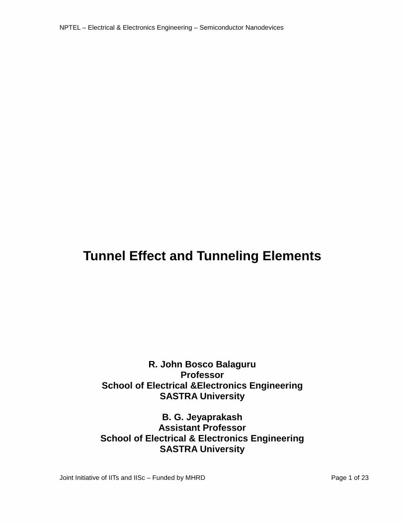
The concept of tunneling plays a significant role in the design and development of nanoelectronic devices. Whenever we connect nano objects like quantum dots to external leads, the concept of tunneling comes in to picture.
Tunneling falls under the domain of Quantum Mechanics: the study of what
happens at the quantum scale. This process cannot be directly perceived, as the understanding is not shaped by macroscopic world, which classical mechanics can adequately explain.
Consider a ball trying to roll over a hill. The following table gives a picture how the perception differs from classical mechanics to that of quantum mechanics.
Classical Mechanics Quantum Mechanics • The ball does not have enough energy
to classically surmount a barrier and thus will not be able to reach the other side. Thus, a ball without sufficient energy to surmount the hill would roll back down
• Lacking the energy to penetrate a wall, it would bounce back (reflection)
• In the extreme case, the ball may bury
itself inside the wall (absorption).
• The ball can, with a very small probability, tunnel to the other side, thus crossing the barrier.
• Here, the ball could, in a sense, borrow energy from its surroundings to tunnel through the wall or roll over the hill, paying it back by making the reflected electrons more energetic than they otherwise would have been
1.1 Reason / Interpretation
• The Heisenberg uncertainty principle, defines a limit on how precisely the position and the momentum of a particle can be known at the same time.
• This implies that there are no solutions with a probability of exactly zero (or one), though a solution may approach infinity.
• For example, the calculation for its position was taken as a probability of 1, the other, i.e. its speed, would have to be infinity. Hence, the probability of a given particle's existence on the opposite side of an intervening barrier is non-zero, and such particles will appear—with no indication of physically transiting the barrier—on the 'other' side with a frequency proportional to this probability.
Joint Initiative of IITs and IISc – Funded by MHRD Page 4 of 23
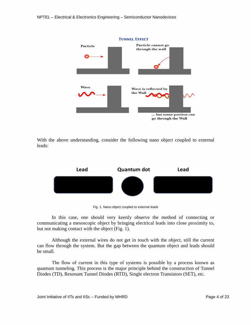
With the above understanding, consider the following nano object coupled to external leads:
Fig. 1. Nano-object coupled to external leads
In this case, one should very keenly observe the method of connecting or communicating a mesoscopic object by bringing electrical leads into close proximity to, but not making contact with the object (Fig. 1).
Although the external wires do not get in touch with the object, still the current can flow through the system. But the gap between the quantum object and leads should be small.
The flow of current in this type of systems is possible by a process known as quantum tunneling. This process is the major principle behind the construction of Tunnel Diodes (TD), Resonant Tunnel Diodes (RTD), Single electron Transistors (SET), etc.
Joint Initiative of IITs and IISc – Funded by MHRD Page 5 of 23
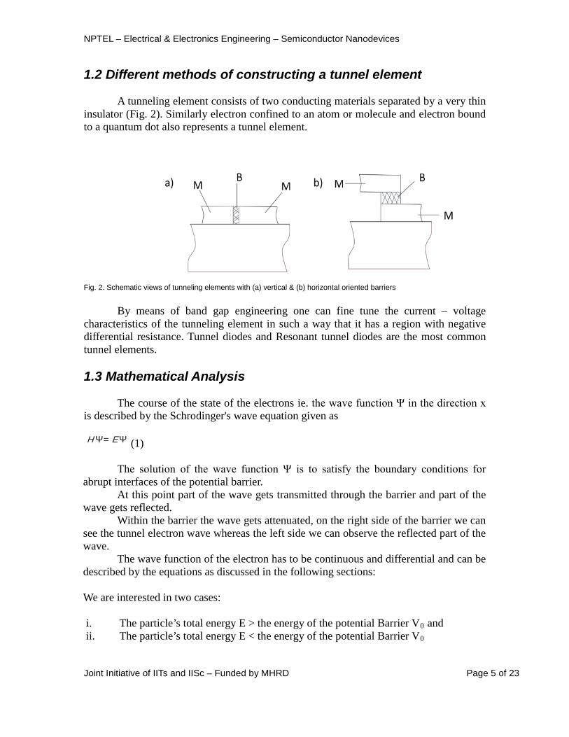
1.2 Different methods of constructing a tunnel element A tunneling element consists of two conducting materials separated by a very thin
insulator (Fig. 2). Similarly electron confined to an atom or molecule and electron bound to a quantum dot also represents a tunnel element.
Fig. 2. Schematic views of tunneling elements with (a) vertical & (b) horizontal oriented barriers
By means of band gap engineering one can fine tune the current – voltage
characteristics of the tunneling element in such a way that it has a region with negative differential resistance. Tunnel diodes and Resonant tunnel diodes are the most common tunnel elements. 1.3 Mathematical Analysis
The course of the state of the electrons ie. the wave function Ψ in the direction x
is described by the Schrodinger's wave equation given as H Ψ= EΨ (1)
The solution of the wave function Ψ is to satisfy the boundary conditions for
abrupt interfaces of the potential barrier. At this point part of the wave gets transmitted through the barrier and part of the
wave gets reflected. Within the barrier the wave gets attenuated, on the right side of the barrier we can
see the tunnel electron wave whereas the left side we can observe the reflected part of the wave.
The wave function of the electron has to be continuous and differential and can be described by the equations as discussed in the following sections: We are interested in two cases: i. The particle’s total energy E > the energy of the potential Barrier V0ii. The particle’s total energy E < the energy of the potential Barrier V
Joint Initiative of IITs and IISc – Funded by MHRD Page 6 of 23
As we have discussed above, the electron can pass through the potential barrier and hence the tunneling process is possible for the second case. How? Consider the Schrodinger wave equation
)()()(2
2*
2
xExxVm
ψ=Ψ
+∇−
(3)
One can note that it is difficult to solve the Eqn. (3) when the potential energy
V(x) varies with the position. It means that the Schrodinger wave equation becomes a non-constant coefficient
differential equation.
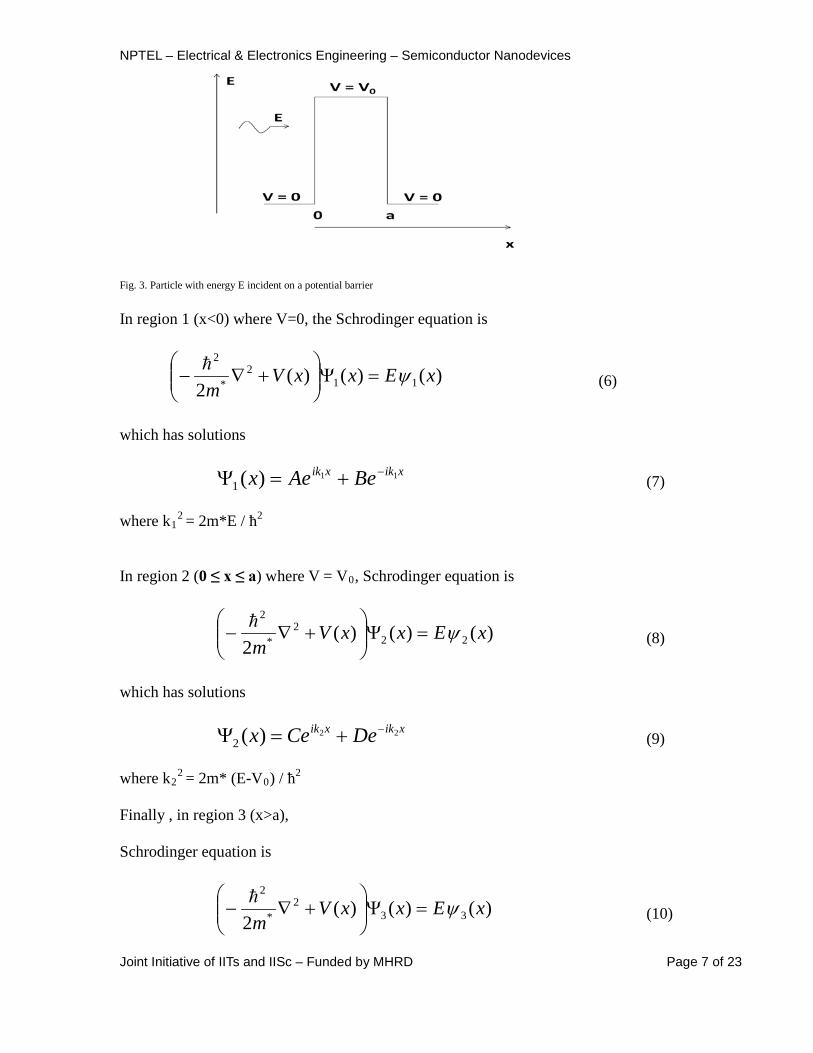
If V(x) is a piecewise constant function, the usual method to avert this problem is to solve Schrodinger’s wave equation separately in each region, as shown in Fig. 3. The regions include:
• first side of the barrier, • at the barrier and • second side of the barrier
where V is independent of the position, and to connect the solutions using the boundary conditions for the wave function, Ψ (x=a-) = Ψ (x=a+) (4) (1/m1)Ψ’ (x=a-) = (1/m2) Ψ’ (x=a+) (5) whereΨ (x=a-) and Ψ (x=a+) are the wave functions in the regions 1 and 2 respectively, infinitesimally close to the transition point. Ψ’ denotes the derivative of Ψ with respect to the position x. The potential energy V(x) profile is shown in Fig. 3. and is given by V = V0 0 ≤ x ≤ a V=0 x<a, x>a
Joint Initiative of IITs and IISc – Funded by MHRD Page 8 of 23
which has solutions
xikxik FeEex 33)(3−+=Ψ (11)
where k3
2 = 2m*E / ħ2 = k1
xikxik BeAex 11)(1−+=Ψ
2 Since there is no potential disturbance to reflect the wave after it reaches the third region, G=0. Therefore we have
xikxik DeCex 22)(2
−+=Ψ xikFex 3)(3 =Ψ (12)
Since the probability density in region 3 is constant, the electron is likely to be found at any point in region 3. By following the boundary conditions (4&5), we obtain
( )( )( ) ( ) 2
2
2221
221
222
21 1
aki
aki
ekkkkekk
AB
−−+−−=
( ) ( ) 2
12
2221
221
)(214
aki
akki
ekkkkekk
AF
−−+=
−
We can define the tunneling probability as
( ) )(4sin)(4
0222
0
02
VEEakVVEE
AFT
−+
−==
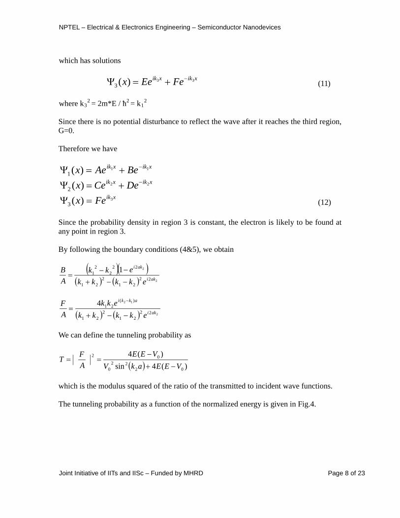
which is the modulus squared of the ratio of the transmitted to incident wave functions. The tunneling probability as a function of the normalized energy is given in Fig.4.
Joint Initiative of IITs and IISc – Funded by MHRD Page 9 of 23
Fig. 4. The tunneling probability as a function of the normalized energy
Due to reflections of the electron wave, all the electrons cannot cross the barrier, even if the total energy is greater than the potential energy of the barrier. 1.4 Conclusions from the variation of tunneling probability as a function of normalized energy
• The tunnel probability increases with increase in the particle energy. • A particle with energy E can tunnel through a barrier with height V• The tunneling probability T is greater for lower and thinner potential barriers.
0.
• The portion of tunneled particles as well as the tunnel current can be gathered from the tunneling probability.
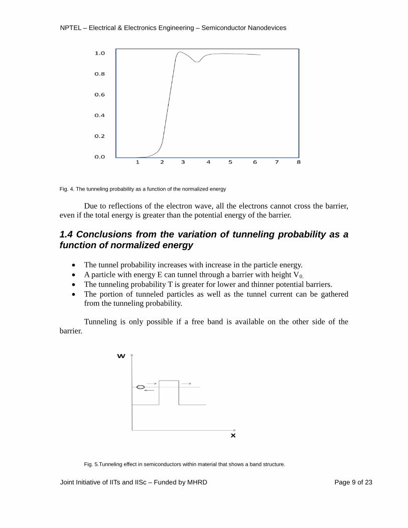
Tunneling is only possible if a free band is available on the other side of the
barrier.
Fig. 5.Tunneling effect in semiconductors within material that shows a band structure.
Joint Initiative of IITs and IISc – Funded by MHRD Page 10 of 23
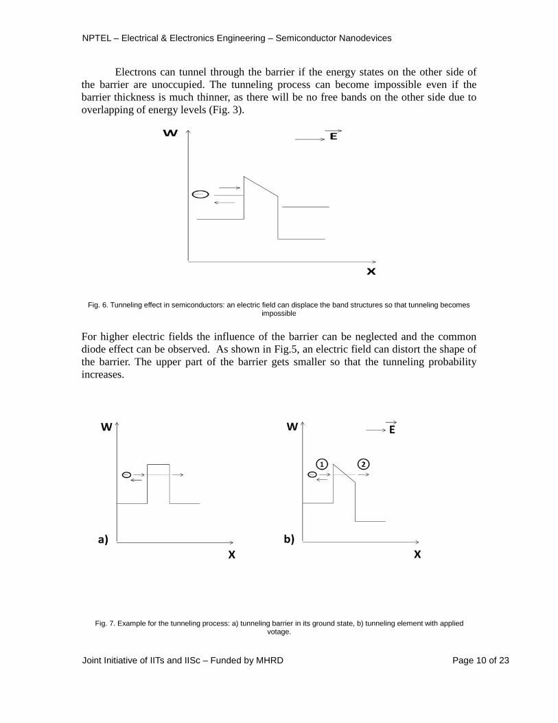
Electrons can tunnel through the barrier if the energy states on the other side of the barrier are unoccupied. The tunneling process can become impossible even if the barrier thickness is much thinner, as there will be no free bands on the other side due to overlapping of energy levels (Fig. 3).
Fig. 6. Tunneling effect in semiconductors: an electric field can displace the band structures so that tunneling becomes
impossible For higher electric fields the influence of the barrier can be neglected and the common diode effect can be observed. As shown in Fig.5, an electric field can distort the shape of the barrier. The upper part of the barrier gets smaller so that the tunneling probability increases.
Fig. 7. Example for the tunneling process: a) tunneling barrier in its ground state, b) tunneling element with applied votage.
Joint Initiative of IITs and IISc – Funded by MHRD Page 11 of 23
Once the electric filed is removed the barrier shape returns to its initial state and the tunneling probability decreases. 1.5 Importance of Tunneling Elements
Tunneling elements form a significant basis for the construction of many
nanoelectronic devices because the electron transport takes place without any loss of energy.
In addition, the switching speed of these elements is very high (in the range of
pico seconds), since the potential barriers are very thin. 2 Tunnel Diode & Resonant Tunnel Diode, Three Terminals Resonant Tunneling Devices – Technology of RTD 2.1 Tunnel Diode
A Tunnel diode is an immediate application of the tunnel element. When a thin insulator is sandwiched between two semiconductors we get a tunnel diode.
Tunnel diode can also be obtained, when the semiconductor is very highly doped (the doping is greater than No) the Fermi level goes above the conduction band for n-type and below valence band for p- type material (degenerate materials) 2.2 Tunnel Diode operation
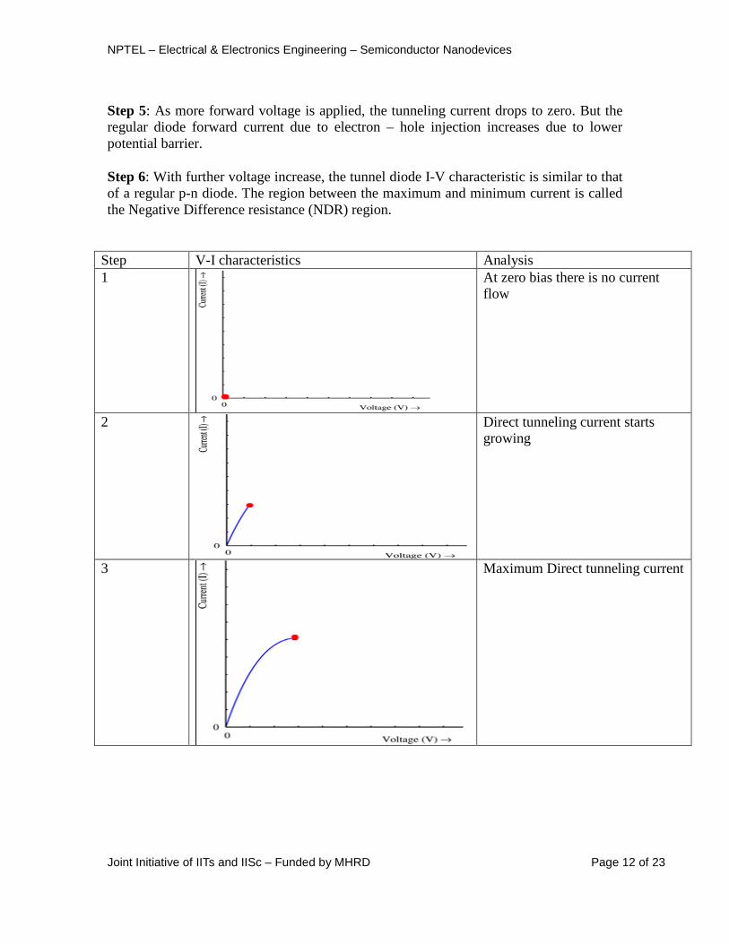
2.2.1 Under Forward Bias Step 1: At zero bias there is no current flow Step 2: A small forward bias is applied. Potential barrier is still very high – no noticeable injection and forward current through the junction. However, electrons in the conduction band of the n region will tunnel to the empty states of the valence band in p region. This will create a forward bias tunnel current Step 3: With a larger voltage the energy of the majority of electrons in the n-region is equal to that of the empty states (holes) in the valence band of p-region; this will produce maximum tunneling current Step 4: As the forward bias continues to increase, the number of electrons in the n side that are directly opposite to the empty states in the valence band (in terms of their energy) decrease. Therefore decrease in the tunneling current will start.
Joint Initiative of IITs and IISc – Funded by MHRD Page 12 of 23
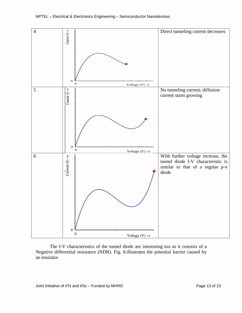
Step 5: As more forward voltage is applied, the tunneling current drops to zero. But the regular diode forward current due to electron – hole injection increases due to lower potential barrier. Step 6: With further voltage increase, the tunnel diode I-V characteristic is similar to that of a regular p-n diode. The region between the maximum and minimum current is called the Negative Difference resistance (NDR) region.
Joint Initiative of IITs and IISc – Funded by MHRD Page 14 of 23
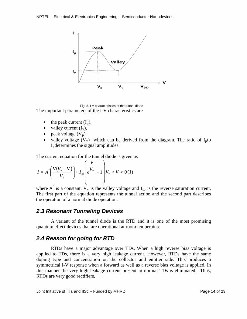
Fig. 8. I-V characteristics of the tunnel diode
The important parameters of the I-V characteristics are
• the peak current (Ip• valley current (I
), v
• peak voltage (V),
p• valley voltage (V
) v) which can be derived from the diagram. The ratio of Ipto
Iv The current equation for the tunnel diode is given as
determines the signal amplitudes.
( )01 >V>V,V
V
eI+V
VVVA=I v
Tso
T
v''
−
− (1)
where A” is a constant. Vv is the valley voltage and Iso is the reverse saturation current. The first part of the equation represents the tunnel action and the second part describes the operation of a normal diode operation. 2.3 Resonant Tunneling Devices
A variant of the tunnel diode is the RTD and it is one of the most promising quantum effect devices that are operational at room temperature.
2.4 Reason for going for RTD
RTDs have a major advantage over TDs. When a high reverse bias voltage is applied to TDs, there is a very high leakage current. However, RTDs have the same doping type and concentration on the collector and emitter side. This produces a symmetrical I-V response when a forward as well as a reverse bias voltage is applied. In this manner the very high leakage current present in normal TDs is eliminated. Thus, RTDs are very good rectifiers.
Joint Initiative of IITs and IISc – Funded by MHRD Page 15 of 23
RTDs have a significant impact in the nanoscale regime. RTDs exhibit a NDR region which can be significantly exploited to make better devices with enhanced performances when compared to the conventional MOS devices.
2.5 Operation
In RTD the band gap alignment consists of twodoped layers (bottom and top
contact layers), two barriers, and one well with at least one bound energy state. When an electric field is applied to electrons, they tunnel from the bottom contact through the barriers, when the bound state in the well is resonant with the Fermi energy level of the bottom layer.
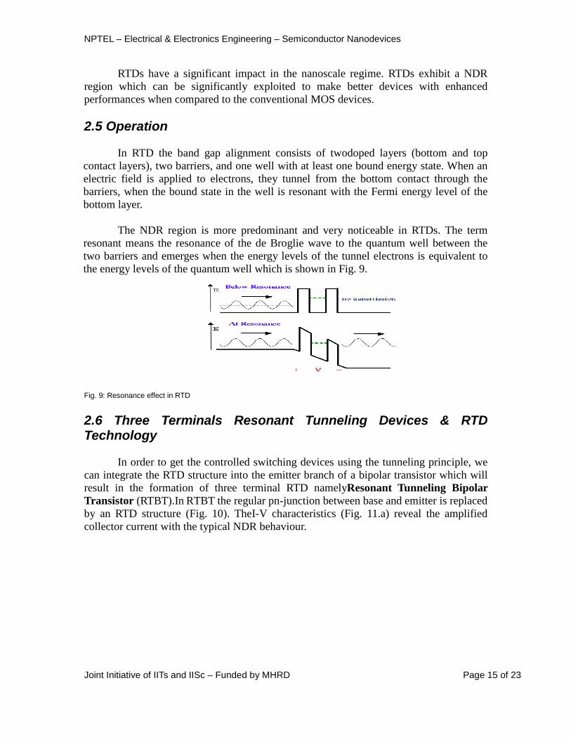
The NDR region is more predominant and very noticeable in RTDs. The term
resonant means the resonance of the de Broglie wave to the quantum well between the two barriers and emerges when the energy levels of the tunnel electrons is equivalent to the energy levels of the quantum well which is shown in Fig. 9. Fig. 9: Resonance effect in RTD 2.6 Three Terminals Resonant Tunneling Devices & RTD Technology
In order to get the controlled switching devices using the tunneling principle, we can integrate the RTD structure into the emitter branch of a bipolar transistor which will result in the formation of three terminal RTD namelyResonant Tunneling Bipolar Transistor (RTBT).In RTBT the regular pn-junction between base and emitter is replaced by an RTD structure (Fig. 10). TheI-V characteristics (Fig. 11.a) reveal the amplified collector current with the typical NDR behaviour.
Joint Initiative of IITs and IISc – Funded by MHRD Page 16 of 23
Fig. 10: Structure of RTBT
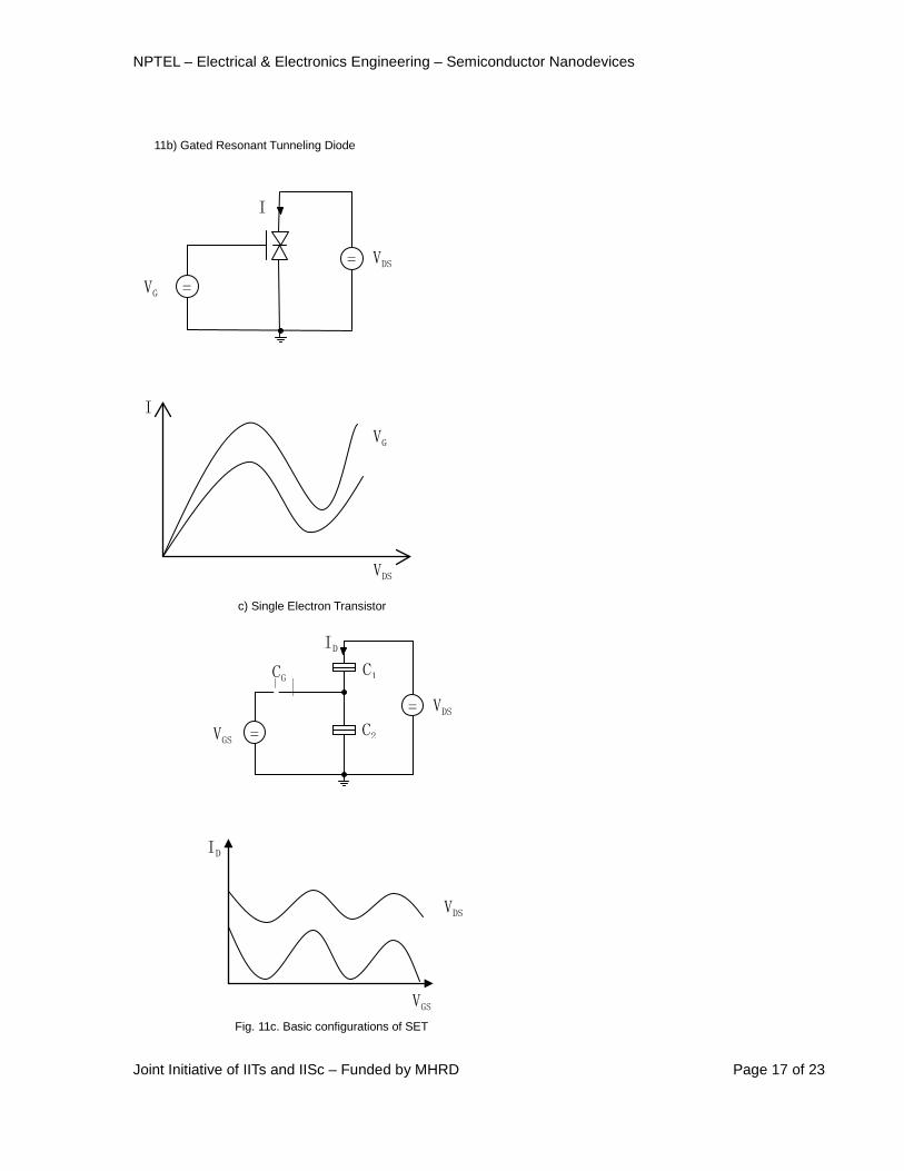
In a similar way the combination of the field effect transistor (FET) with an RTD.
Serial and parallel combinations of these two devices show the negative differential resistance (Fig. 11b). In both cases the I-V characteristics can be altered by the gate voltage of the FET. Fig. 11c shows another nanoelectronic device namely single-electron transistor (SET) that consists of small capacitances and two tunneling elements. Here also one can observe NDR regions in its I-V characteristics that are typical of all quantum-effect devices.
Joint Initiative of IITs and IISc – Funded by MHRD Page 18 of 23
3 Applications of RTDs
RTDs have attracted a lot of attention and have been researched for almost two decades because of their compatibility with many conventional technologies such as high electron mobility transistors (HEMTs) and metal oxide field effect transistors (MOSFETs). The high-speed, low power benefits can now be applied to digital circuit applications. 3.1 Logic Gates Using RTDs
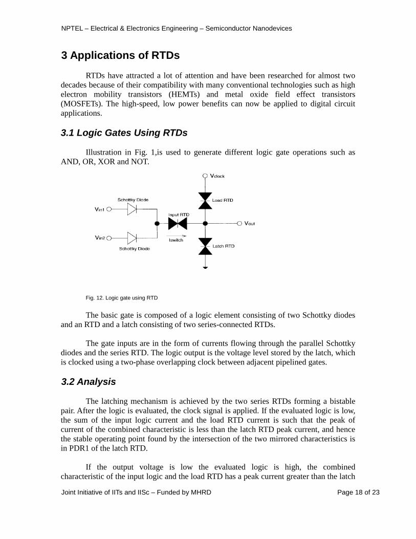
Illustration in Fig. 1,is used to generate different logic gate operations such as AND, OR, XOR and NOT.
Fig. 12. Logic gate using RTD The basic gate is composed of a logic element consisting of two Schottky diodes
and an RTD and a latch consisting of two series-connected RTDs. The gate inputs are in the form of currents flowing through the parallel Schottky
diodes and the series RTD. The logic output is the voltage level stored by the latch, which is clocked using a two-phase overlapping clock between adjacent pipelined gates.
3.2 Analysis
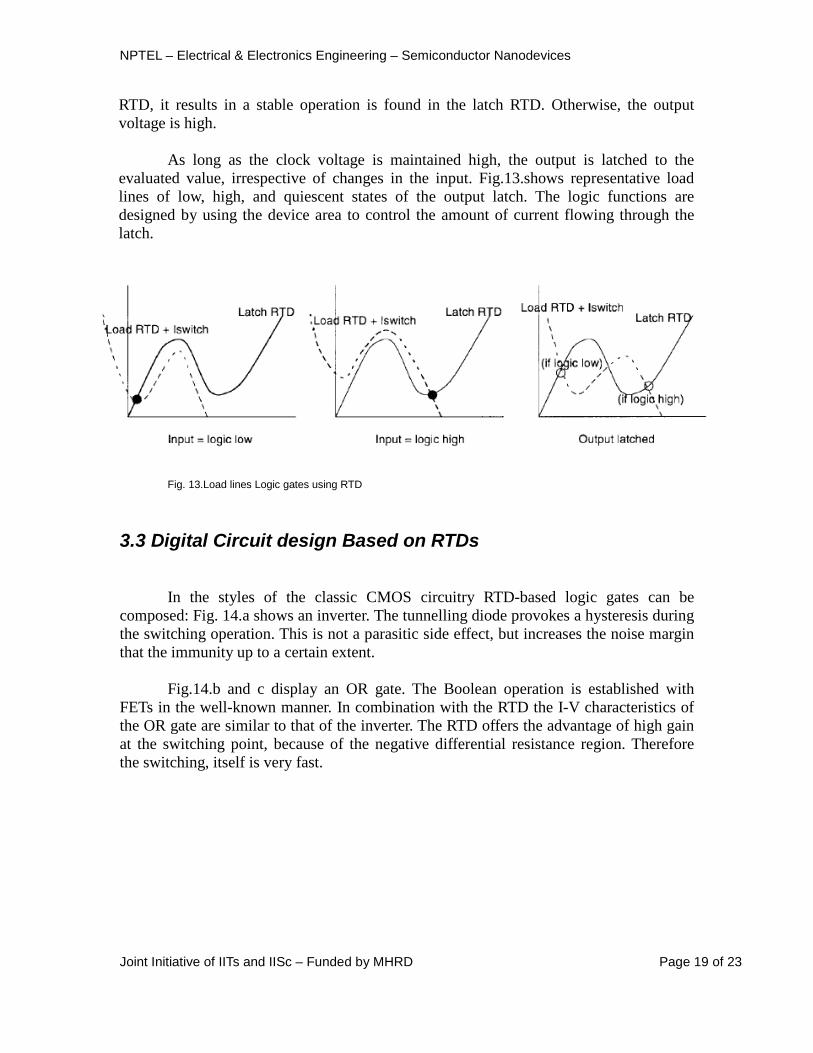
The latching mechanism is achieved by the two series RTDs forming a bistable pair. After the logic is evaluated, the clock signal is applied. If the evaluated logic is low, the sum of the input logic current and the load RTD current is such that the peak of current of the combined characteristic is less than the latch RTD peak current, and hence the stable operating point found by the intersection of the two mirrored characteristics is in PDR1 of the latch RTD.
If the output voltage is low the evaluated logic is high, the combined characteristic of the input logic and the load RTD has a peak current greater than the latch
Joint Initiative of IITs and IISc – Funded by MHRD Page 19 of 23
RTD, it results in a stable operation is found in the latch RTD. Otherwise, the output voltage is high.
As long as the clock voltage is maintained high, the output is latched to the
evaluated value, irrespective of changes in the input. Fig.13.shows representative load lines of low, high, and quiescent states of the output latch. The logic functions are designed by using the device area to control the amount of current flowing through the latch.
Fig. 13.Load lines Logic gates using RTD
3.3 Digital Circuit design Based on RTDs
In the styles of the classic CMOS circuitry RTD-based logic gates can be composed: Fig. 14.a shows an inverter. The tunnelling diode provokes a hysteresis during the switching operation. This is not a parasitic side effect, but increases the noise margin that the immunity up to a certain extent.
Fig.14.b and c display an OR gate. The Boolean operation is established with
FETs in the well-known manner. In combination with the RTD the I-V characteristics of the OR gate are similar to that of the inverter. The RTD offers the advantage of high gain at the switching point, because of the negative differential resistance region. Therefore the switching, itself is very fast.
Joint Initiative of IITs and IISc – Funded by MHRD Page 21 of 23
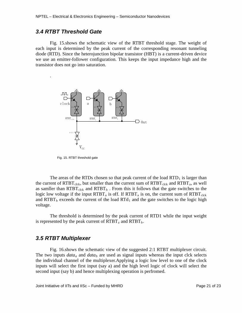
3.4 RTBT Threshold Gate Fig. 15.shows the schematic view of the RTBT threshold stage. The weight of each input is determined by the peak current of the corresponding resonant tunneling diode (RTD). Since the heterojunction bipolar transistor (HBT) is a current-driven device we use an emitter-follower configuration. This keeps the input impedance high and the transistor does not go into saturation.
.
The areas of the RTDs chosen so that peak current of the load RTD1 is larger than the current of RTBTclck, but smaller than the current sum of RTBTclck and RTBTa, as well as samller than RTBTclck and RTBTb . From this it follows that the gate switches to the logic low voltage if the input RTBTa is off. If RTBTa is on, the current sum of RTBTclck and RTBTb exceeds the current of the load RTd1 and the gate switches to the logic high voltage.
The threshold is determined by the peak current of RTD1 while the input weight is represented by the peak current of RTBTa and RTBTb. 3.5 RTBT Multiplexer
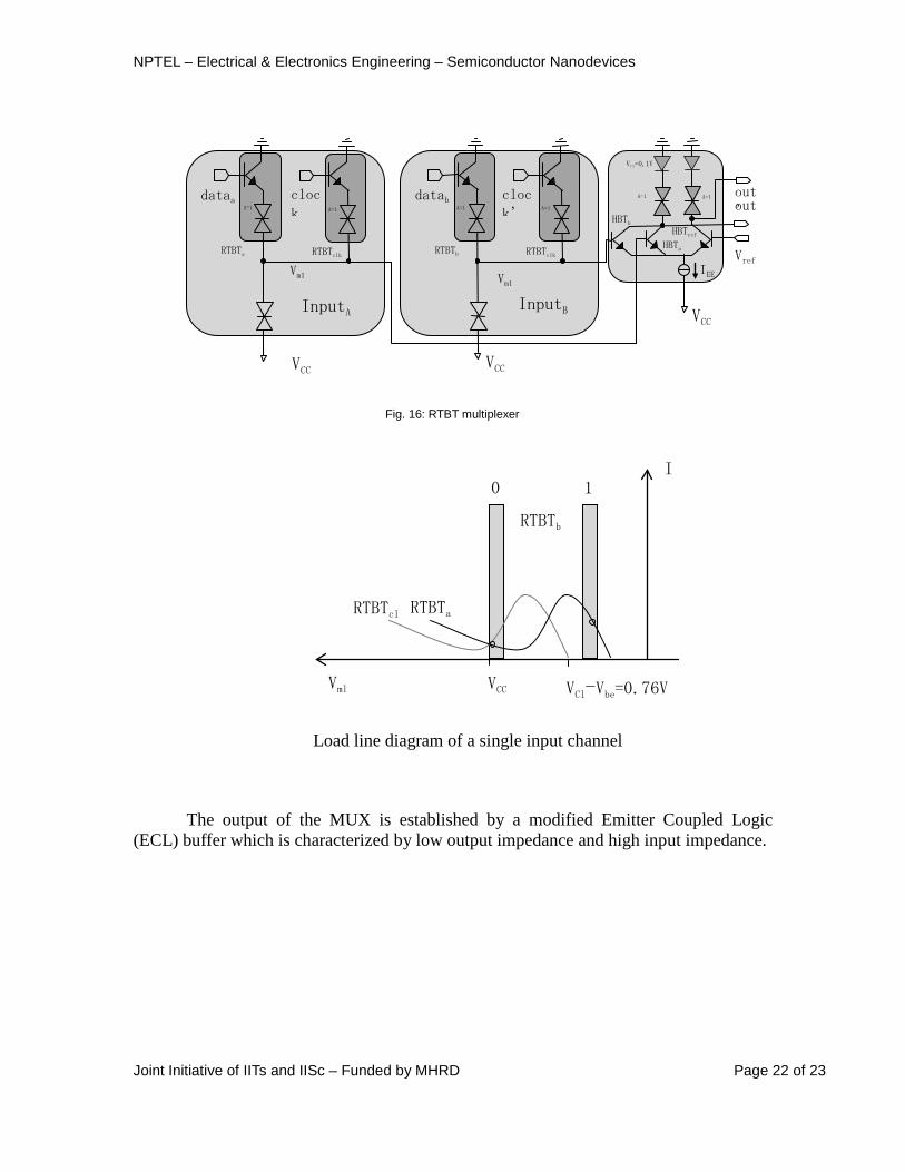
Fig. 16.shows the schematic view of the suggested 2:1 RTBT multiplexer circuit. The two inputs dataa and datab are used as signal inputs whereas the input clck selects the individual channel of the multiplexer.Applying a logic low level to one of the clock inputs will select the first input (say a) and the high level logic of clock will select the second input (say b) and hence multiplexing operation is perfromed.