An IMPORTANT NOTICE at the end of this data sheet addresses availability, warranty, changes, use in safety-critical applications,intellectual property matters and other important disclaimers. PRODUCTION DATA.
TUSB211, TUSB211ISLLSEO0D –MAY 2015–REVISED OCTOBER 2017
TUSB211 USB 2.0 High Speed Signal Conditioner
1
1 Features1• Compatible with USB 2.0, OTG 2.0 and BC 1.2• Support for LS, FS, HS signaling• Active Power Consumption of 55 mW (Typical)
with 3.3-V Single Supply• Selectable Signal Gain Via External Pulldown
Resistor• Does Not Break DP, DM Trace• Scalable Solution – Daisy Chain Device for High
Loss Applications• Compact 1.6 mm x 1.6 mm QFN Package
3 DescriptionThe TUSB211 is a USB High-Speed (HS) signalconditioner, designed to compensate for ISI signalloss in a transmission channel.
The device has a patent-pending design which isagnostic to USB Low Speed (LS) and Full Speed(FS) signals. LS and FS signal characteristics areunaffected by the TUSB211. HS signals arecompensated.
Programmable signal gain permits fine tuning deviceperformance to optimize High Speed signals at theconnector. This helps to pass USB High Speedelectrical compliance tests.
The footprint of TUSB211 does not break thecontinuity of the DP/DM signal path. This permits riskfree system design of a complete USB channel.
In addition, TUSB211 is compatible with the USB On-The-Go (OTG) and Battery Charging (BC) protocols
Device Information (1)
PART NUMBER PACKAGE BODY SIZE (NOM)TUSB211
X2QFN (12) 1.60 mm x 1.60 mmTUSB211I
(1) For all available packages, see the orderable addendum atthe end of the datasheet.
9 Power Supply Recommendations ...................... 1110 Layout................................................................... 12
10.1 Layout Guidelines ................................................. 1210.2 Layout Example .................................................... 12
11 Device and Documentation Support ................. 1311.1 Related Links ........................................................ 1311.2 Community Resources.......................................... 1311.3 Trademarks ........................................................... 1311.4 Electrostatic Discharge Caution............................ 1311.5 Glossary ................................................................ 13
12 Mechanical, Packaging, and OrderableInformation ........................................................... 13
4 Revision History
Changes from Revision C (June 2016) to Revision D Page
• Deleted device TUSB211-Q1 From the data sheet................................................................................................................ 1• Deleted Features: Qualified for Automotive Applications ....................................................................................................... 1• Deleted Applications: Automotive Infotainment ...................................................................................................................... 1
Changes from Revision A (June 2015) to Revision B Page
• Changed From: 1-page datasheet To: Full datasheet .......................................................................................................... 1• Added Features: Qualified for Automotive Applications ......................................................................................................... 1• Deleted Features: –40°C to 85°C Industrial Temperature Range.......................................................................................... 1• Added Applications: Automotive Infotainment ........................................................................................................................ 1• Changed the Simplified Schematic......................................................................................................................................... 1
Changes from Original (May 2015) to Revision A Page
• Changed the data sheet From: Product Preview To: Production .......................................................................................... 1
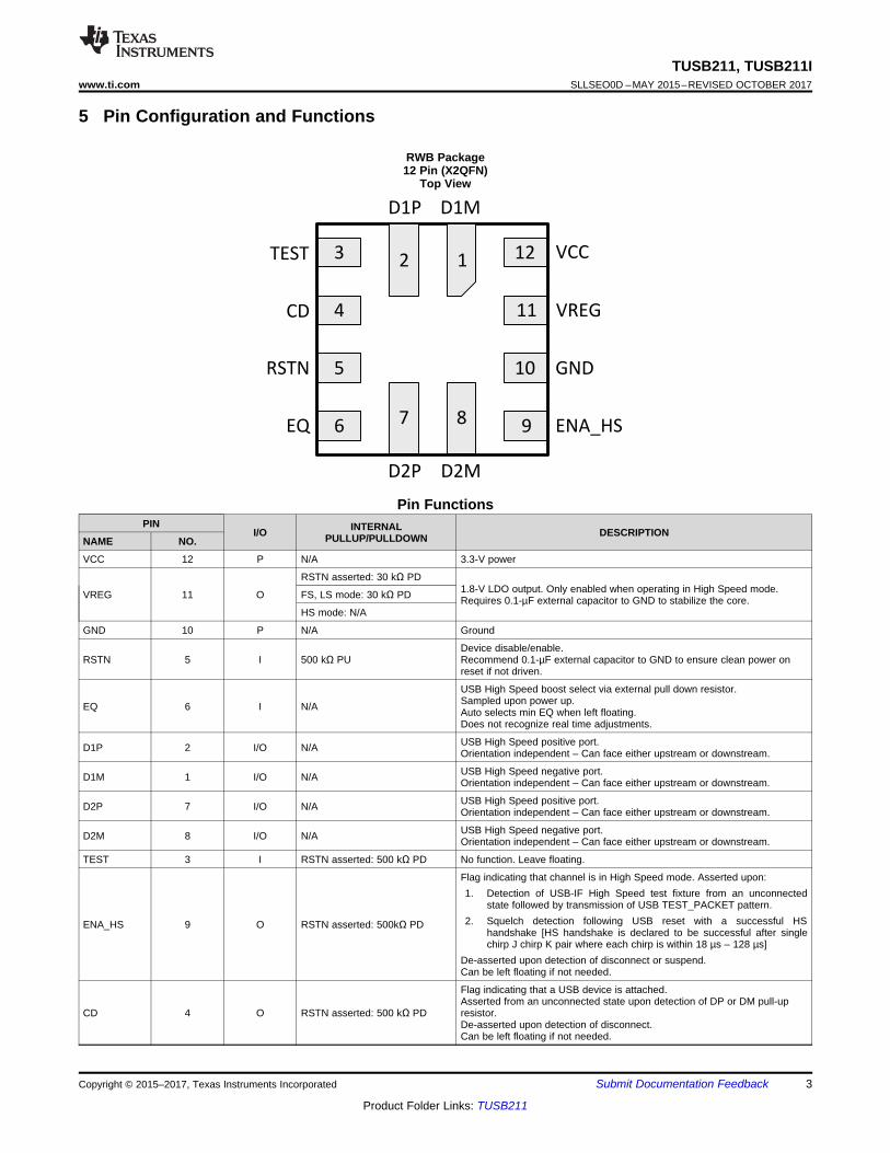
RSTN asserted: 30 kΩ PD1.8-V LDO output. Only enabled when operating in High Speed mode.Requires 0.1-µF external capacitor to GND to stabilize the core.FS, LS mode: 30 kΩ PD
HS mode: N/A
GND 10 P N/A Ground
RSTN 5 I 500 kΩ PUDevice disable/enable.Recommend 0.1-µF external capacitor to GND to ensure clean power onreset if not driven.
EQ 6 I N/A
USB High Speed boost select via external pull down resistor.Sampled upon power up.Auto selects min EQ when left floating.Does not recognize real time adjustments.
D1P 2 I/O N/A USB High Speed positive port.Orientation independent – Can face either upstream or downstream.
D1M 1 I/O N/A USB High Speed negative port.Orientation independent – Can face either upstream or downstream.
D2P 7 I/O N/A USB High Speed positive port.Orientation independent – Can face either upstream or downstream.
D2M 8 I/O N/A USB High Speed negative port.Orientation independent – Can face either upstream or downstream.
TEST 3 I RSTN asserted: 500 kΩ PD No function. Leave floating.
ENA_HS 9 O RSTN asserted: 500kΩ PD
Flag indicating that channel is in High Speed mode. Asserted upon:1. Detection of USB-IF High Speed test fixture from an unconnected
state followed by transmission of USB TEST_PACKET pattern.2. Squelch detection following USB reset with a successful HS
handshake [HS handshake is declared to be successful after singlechirp J chirp K pair where each chirp is within 18 µs – 128 µs]
De-asserted upon detection of disconnect or suspend.Can be left floating if not needed.
CD 4 O RSTN asserted: 500 kΩ PD
Flag indicating that a USB device is attached.Asserted from an unconnected state upon detection of DP or DM pull-upresistor.De-asserted upon detection of disconnect.Can be left floating if not needed.
(1) Stresses beyond those listed under Absolute Maximum Ratings may cause permanent damage to the device. These are stress ratingsonly, which do not imply functional operation of the device at these or any other conditions beyond those indicated under RecommendedOperating Conditions. Exposure to absolute-maximum-rated conditions for extended periods may affect device reliability.
6 Specifications
6.1 Absolute Maximum Ratingsover operating free-air temperature range (unless otherwise noted) (1)
MIN MAX UNITSupply voltage range VCC –0.3 3.8 VVoltage range D1P, D1M, D2P, D2M, RSTN, EQ –0.3 3.8 VStorage temperature, Tstg –65 150 °C
(1) JEDEC document JEP155 states that 500-V HBM allows safe manufacturing with a standard ESD control process.(2) JEDEC document JEP157 states that 250-V CDM allows safe manufacturing with a standard ESD control process.
6.2 ESD RatingsVALUE UNIT
V(ESD) Electrostatic dischargeHuman-body model (HBM), per ANSI/ESDA/JEDEC JS-001 (1) ±3000
VCharged-device model (CDM), per JEDEC specification JESD22-C101(2) ±1000
6.3 Recommended Operating Conditionsover operating free-air temperature range (unless otherwise noted)
MIN NOM MAX UNITVCC Supply voltage 3 3.3 3.6 V
TAOperating free-air temperature [TUSB211] 0 70
°COperating free-air temperature [TUSB211I] –40 85
(1) For more information about traditional and new thermal metrics, see the Semiconductor and IC Package Thermal Metrics applicationreport, SPRA953.
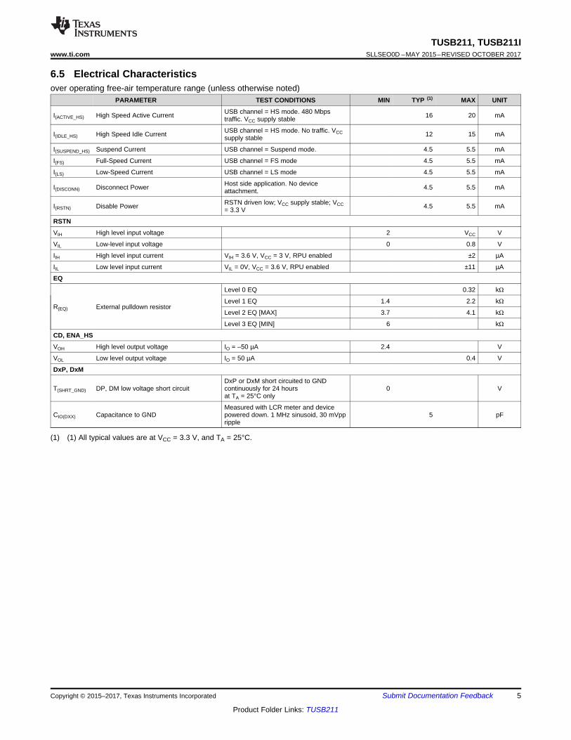
(1) (1) All typical values are at VCC = 3.3 V, and TA = 25°C.
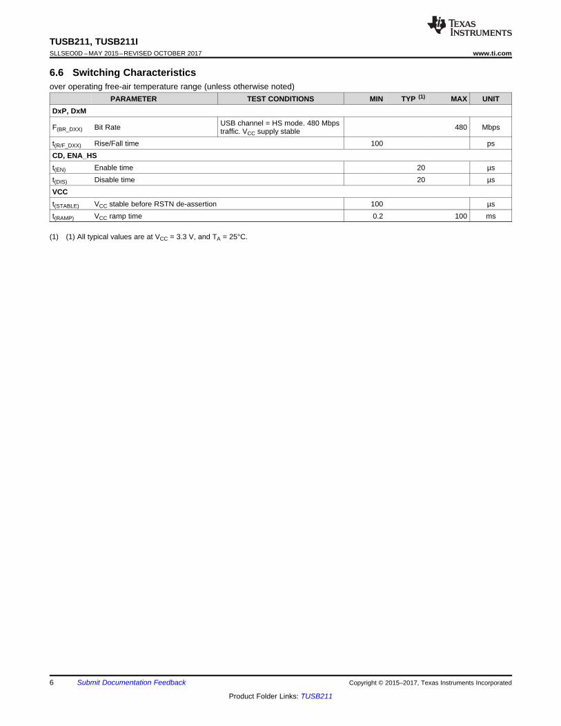
6.6 Switching Characteristicsover operating free-air temperature range (unless otherwise noted)
PARAMETER TEST CONDITIONS MIN TYP (1) MAX UNITDxP, DxM
F(BR_DXX) Bit Rate USB channel = HS mode. 480 Mbpstraffic. VCC supply stable 480 Mbps
t(R/F_DXX) Rise/Fall time 100 psCD, ENA_HSt(EN) Enable time 20 µst(DIS) Disable time 20 µsVCCt(STABLE) VCC stable before RSTN de-assertion 100 µst(RAMP) VCC ramp time 0.2 100 ms
7.1 OverviewThe TUSB211 is a USB High-Speed (HS) signal conditioner, designed to compensate for ISI signal loss in atransmission channel. TUSB211 has a patent-pending design which is agnostic to USB Low Speed (LS) and FullSpeed (FS) signals and does not alter their signal characteristics, while HS signals are compensated. In addition,the design is compatible with USB On-The-Go (OTG) and Battery Charging (BC) specifications.
Programmable signal gain through an external resistor permits fine tuning device performance to optimize signalshelping to pass USB HS electrical compliance tests at the connector.
The footprint of TUSB211 allows a board layout using this device such that it does not break the continuity of theDP/DM signal traces. This permits risk free system design of a complete USB channel with flexible use of one ormultiple TUSB211 devices as needed for optimal signal integrity. This allows system designers to plan for thisdevice and use it only if signal integrity analysis and/or lab measurements show a need. If such a need is notwarranted, the device can be left unpopulated without any board rework.
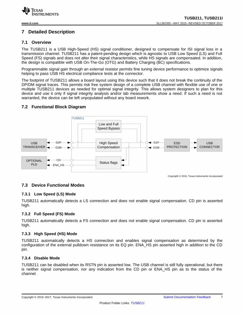
7.2 Functional Block Diagram
7.3 Device Functional Modes
7.3.1 Low Speed (LS) ModeTUSB211 automatically detects a LS connection and does not enable signal compensation. CD pin is assertedhigh.
7.3.2 Full Speed (FS) ModeTUSB211 automatically detects a FS connection and does not enable signal compensation. CD pin is assertedhigh.
7.3.3 High Speed (HS) ModeTUSB211 automatically detects a HS connection and enables signal compensation as determined by theconfiguration of the external pulldown resistance on its EQ pin. ENA_HS pin asserted high in addition to the CDpin.
7.3.4 Disable ModeTUSB211 can be disabled when its RSTN pin is asserted low. The USB channel is still fully operational, but thereis neither signal compensation, nor any indication from the CD pin or ENA_HS pin as to the status of thechannel.
NOTEInformation in the following applications sections is not part of the TI componentspecification, and TI does not warrant its accuracy or completeness. TI’s customers areresponsible for determining suitability of components for their purposes. Customers shouldvalidate and test their design implementation to confirm system functionality.
8.1 Application InformationThe primary purpose of the TUSB211 is to re-store the signal integrity of a USB High Speed channel up to theUSB connector. The loss in signal quality stems from reduced channel bandwidth due to high loss PCB trace andother components that contribute a capacitive load. This can cause the channel to fail the USB near end eyemask. Proper use of the TUSB211 can help to pass this eye mask.
A secondary purpose is to use the CD pin and ENA_HS pin of the TUSB211 to control other blocks on thecustomer platform if so desired.
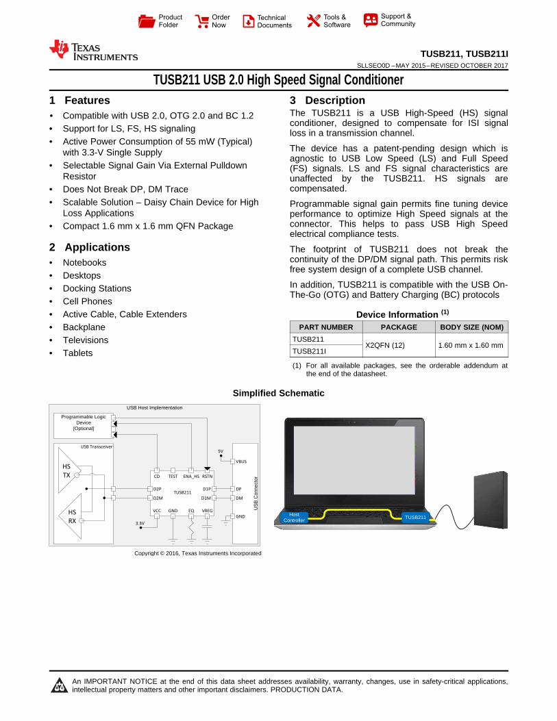
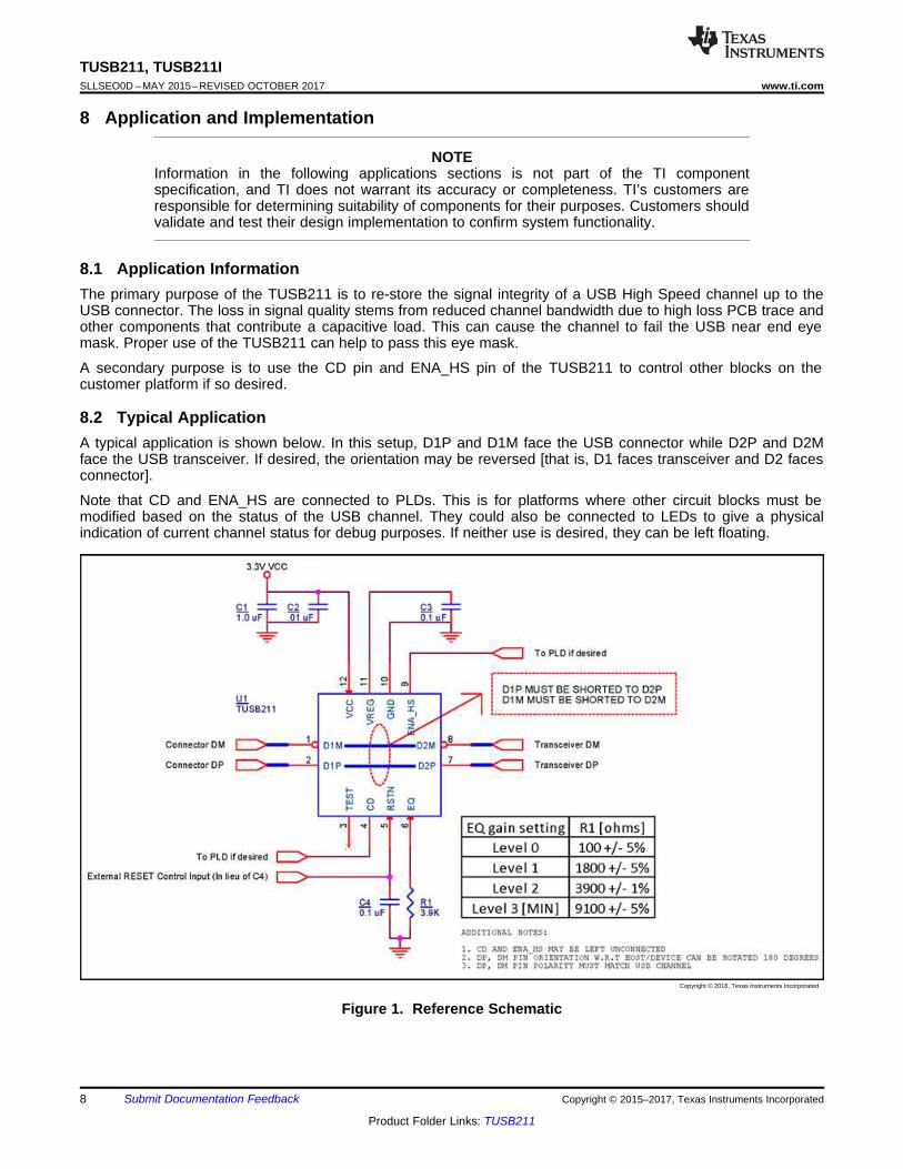
8.2 Typical ApplicationA typical application is shown below. In this setup, D1P and D1M face the USB connector while D2P and D2Mface the USB transceiver. If desired, the orientation may be reversed [that is, D1 faces transceiver and D2 facesconnector].
Note that CD and ENA_HS are connected to PLDs. This is for platforms where other circuit blocks must bemodified based on the status of the USB channel. They could also be connected to LEDs to give a physicalindication of current channel status for debug purposes. If neither use is desired, they can be left floating.
Typical Application (continued)8.2.1 Design RequirementsTUSB211 requires a valid reset signal as described in the power supply recommendations section. The capacitorC4 is not required if a microcontroller drives the RSTN pin according to recommendations.
Pin 11 VREG is an internal LDO output that requires a 0.1 μF external capacitor to GND to stabilize the core.
Pin 6 EQ requires an external pulldown resistor if EQ levels 0-2 are needed. If EQ level 3 is needed, then the EQpin can be left floating.
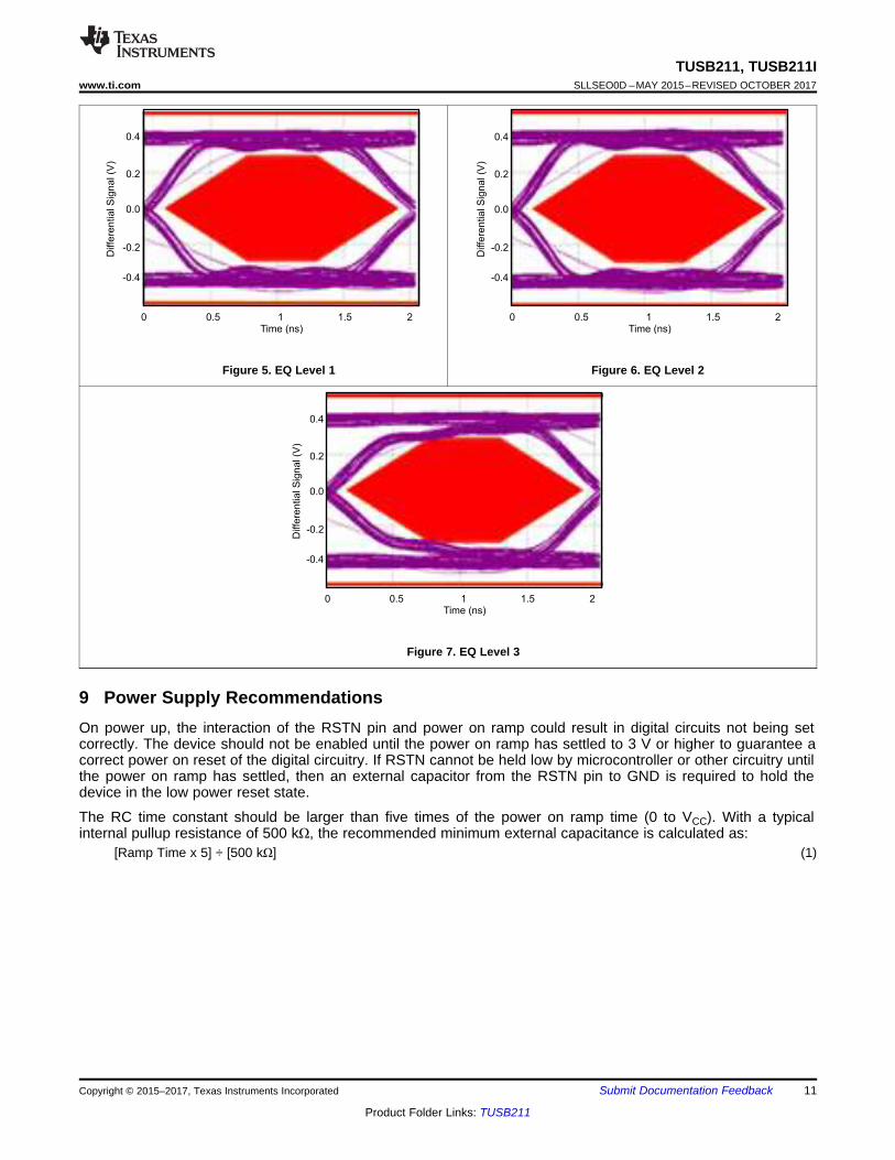
8.2.2 Detailed Design ProcedureThe ideal EQ setting is dependent upon the signal chain loss characteristics of the target platform. The generalrecommendation is to start with EQ level 0, and then increment to EQ level 1, and so on. if permissible.
In order for the TUSB211 to recognize any change to the EQ setting, the RSTN pin must be toggled. This isbecause the EQ pin is latched on power up and the pin is ignored thereafter.
In addition, TUSB211 does not compensate for any DC attenuation in the signal path. Therefore, minimizing DCloss (that is, resistance) in the system design, is suggested. As a consequence, this might lead to increased linecapacitance. This is acceptable because the TUSB211 can compensate for the additional capacitive load.
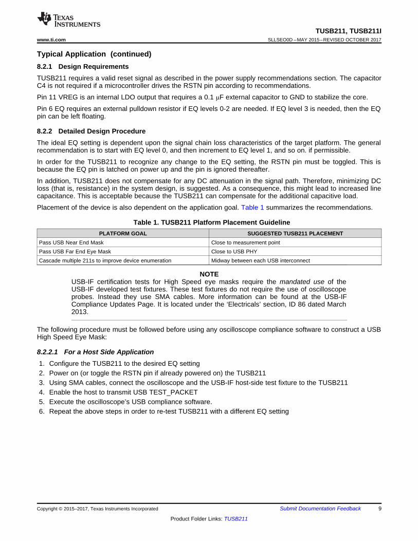
Placement of the device is also dependent on the application goal. Table 1 summarizes the recommendations.
Pass USB Near End Mask Close to measurement pointPass USB Far End Eye Mask Close to USB PHYCascade multiple 211s to improve device enumeration Midway between each USB interconnect
NOTEUSB-IF certification tests for High Speed eye masks require the mandated use of theUSB-IF developed test fixtures. These test fixtures do not require the use of oscilloscopeprobes. Instead they use SMA cables. More information can be found at the USB-IFCompliance Updates Page. It is located under the ‘Electricals’ section, ID 86 dated March2013.
The following procedure must be followed before using any oscilloscope compliance software to construct a USBHigh Speed Eye Mask:
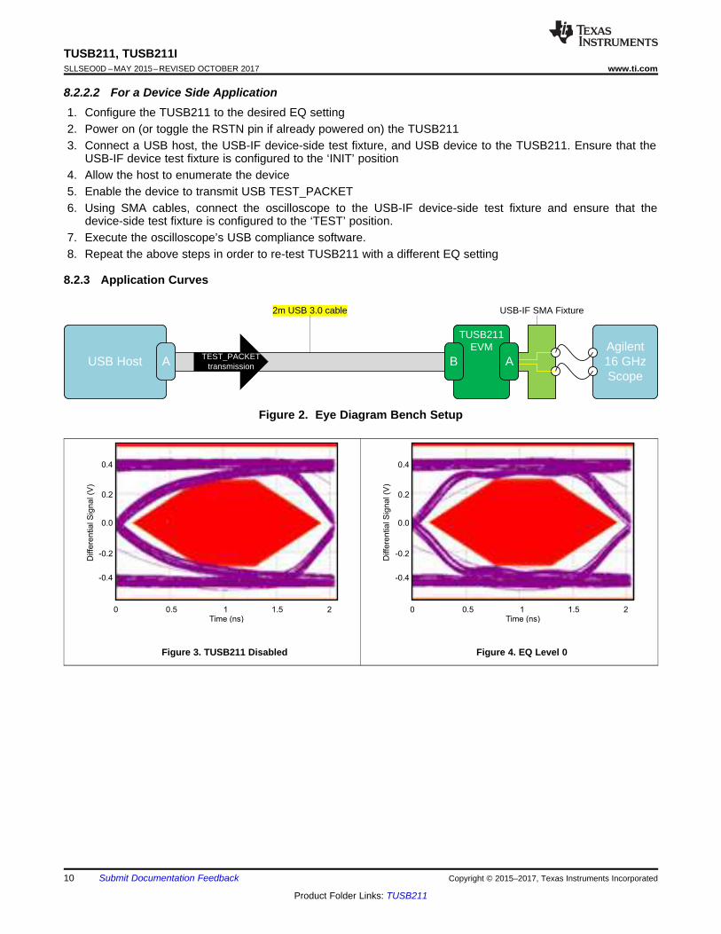
8.2.2.1 For a Host Side Application1. Configure the TUSB211 to the desired EQ setting2. Power on (or toggle the RSTN pin if already powered on) the TUSB2113. Using SMA cables, connect the oscilloscope and the USB-IF host-side test fixture to the TUSB2114. Enable the host to transmit USB TEST_PACKET5. Execute the oscilloscope’s USB compliance software.6. Repeat the above steps in order to re-test TUSB211 with a different EQ setting
8.2.2.2 For a Device Side Application1. Configure the TUSB211 to the desired EQ setting2. Power on (or toggle the RSTN pin if already powered on) the TUSB2113. Connect a USB host, the USB-IF device-side test fixture, and USB device to the TUSB211. Ensure that the
USB-IF device test fixture is configured to the ‘INIT’ position4. Allow the host to enumerate the device5. Enable the device to transmit USB TEST_PACKET6. Using SMA cables, connect the oscilloscope to the USB-IF device-side test fixture and ensure that the
device-side test fixture is configured to the ‘TEST’ position.7. Execute the oscilloscope’s USB compliance software.8. Repeat the above steps in order to re-test TUSB211 with a different EQ setting
9 Power Supply RecommendationsOn power up, the interaction of the RSTN pin and power on ramp could result in digital circuits not being setcorrectly. The device should not be enabled until the power on ramp has settled to 3 V or higher to guarantee acorrect power on reset of the digital circuitry. If RSTN cannot be held low by microcontroller or other circuitry untilthe power on ramp has settled, then an external capacitor from the RSTN pin to GND is required to hold thedevice in the low power reset state.
The RC time constant should be larger than five times of the power on ramp time (0 to VCC). With a typicalinternal pullup resistance of 500 kΩ, the recommended minimum external capacitance is calculated as:
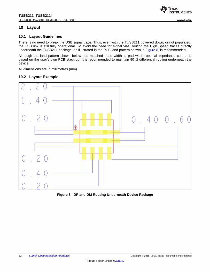
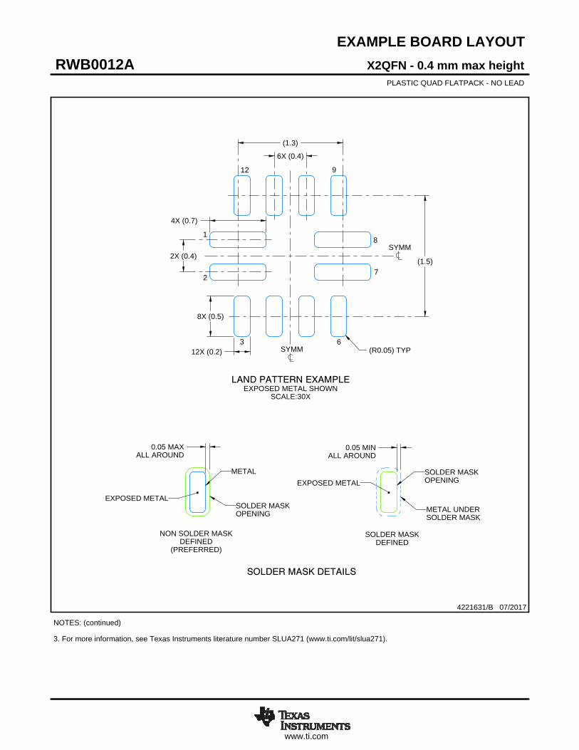
10.1 Layout GuidelinesThere is no need to break the USB signal trace. Thus, even with the TUSB211 powered down, or not populated,the USB link is still fully operational. To avoid the need for signal vias, routing the High Speed traces directlyunderneath the TUSB211 package, as illustrated in the PCB land pattern shown in Figure 8, is recommended.
Although the land pattern shown below has matched trace width to pad width, optimal impedance control isbased on the user's own PCB stack-up. It is recommended to maintain 90 Ω differential routing underneath thedevice.
All dimensions are in millimetres (mm).
10.2 Layout Example
Figure 8. DP and DM Routing Underneath Device Package
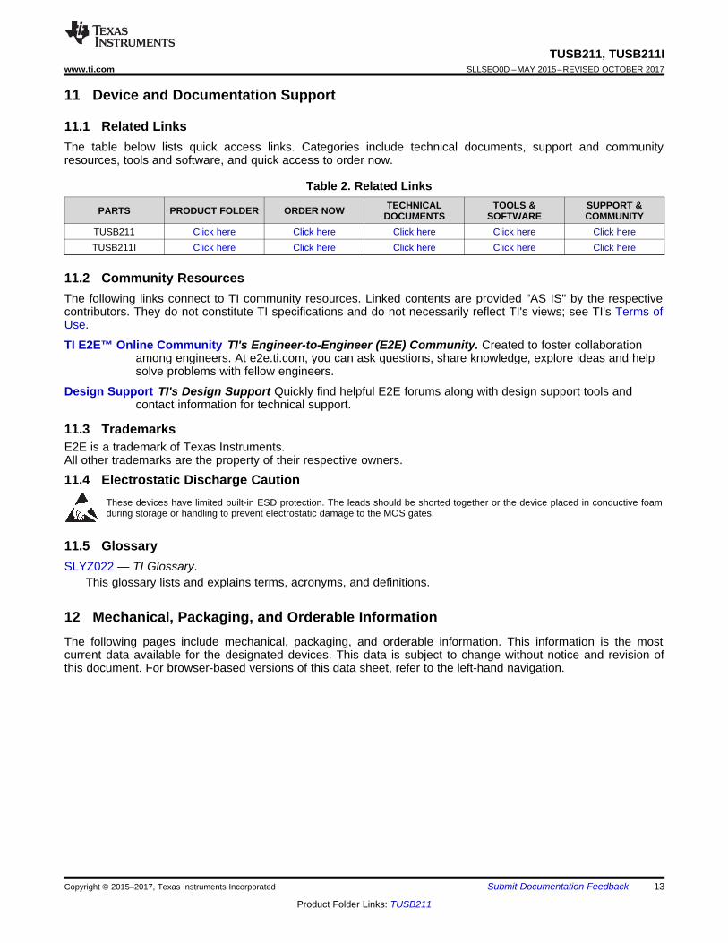
11.1 Related LinksThe table below lists quick access links. Categories include technical documents, support and communityresources, tools and software, and quick access to order now.
Table 2. Related Links
PARTS PRODUCT FOLDER ORDER NOW TECHNICALDOCUMENTS
TOOLS &SOFTWARE
SUPPORT &COMMUNITY
TUSB211 Click here Click here Click here Click here Click hereTUSB211I Click here Click here Click here Click here Click here
11.2 Community ResourcesThe following links connect to TI community resources. Linked contents are provided "AS IS" by the respectivecontributors. They do not constitute TI specifications and do not necessarily reflect TI's views; see TI's Terms ofUse.
TI E2E™ Online Community TI's Engineer-to-Engineer (E2E) Community. Created to foster collaborationamong engineers. At e2e.ti.com, you can ask questions, share knowledge, explore ideas and helpsolve problems with fellow engineers.
Design Support TI's Design Support Quickly find helpful E2E forums along with design support tools andcontact information for technical support.
11.3 TrademarksE2E is a trademark of Texas Instruments.All other trademarks are the property of their respective owners.
11.4 Electrostatic Discharge CautionThese devices have limited built-in ESD protection. The leads should be shorted together or the device placed in conductive foamduring storage or handling to prevent electrostatic damage to the MOS gates.
11.5 GlossarySLYZ022 — TI Glossary.
This glossary lists and explains terms, acronyms, and definitions.
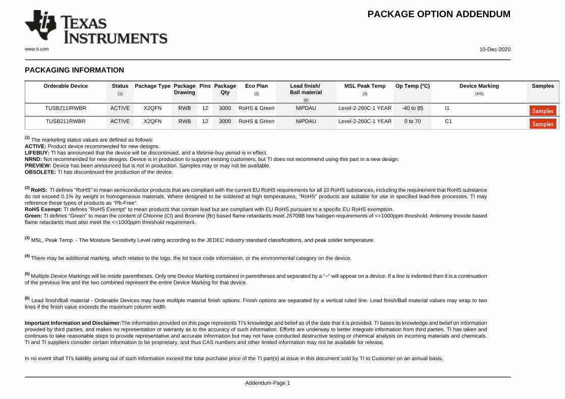
12 Mechanical, Packaging, and Orderable InformationThe following pages include mechanical, packaging, and orderable information. This information is the mostcurrent data available for the designated devices. This data is subject to change without notice and revision ofthis document. For browser-based versions of this data sheet, refer to the left-hand navigation.
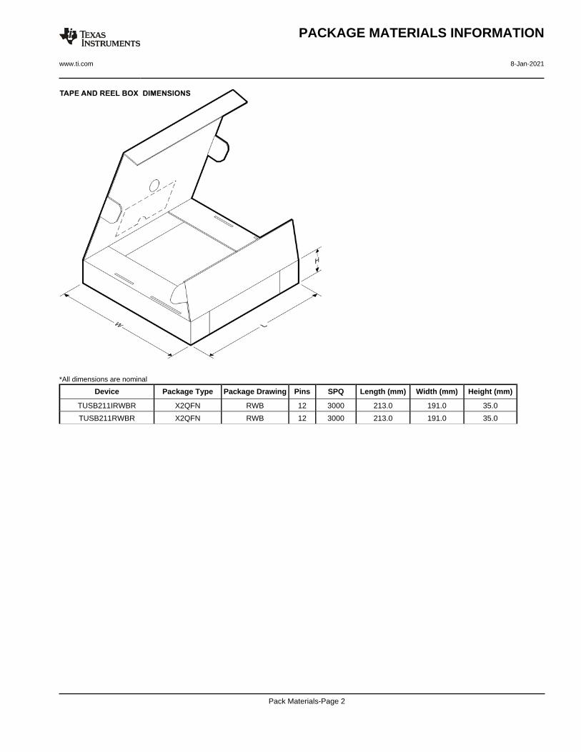
TUSB211IRWBR ACTIVE X2QFN RWB 12 3000 RoHS & Green NIPDAU Level-2-260C-1 YEAR -40 to 85 I1
TUSB211RWBR ACTIVE X2QFN RWB 12 3000 RoHS & Green NIPDAU Level-2-260C-1 YEAR 0 to 70 C1
(1) The marketing status values are defined as follows:ACTIVE: Product device recommended for new designs.LIFEBUY: TI has announced that the device will be discontinued, and a lifetime-buy period is in effect.NRND: Not recommended for new designs. Device is in production to support existing customers, but TI does not recommend using this part in a new design.PREVIEW: Device has been announced but is not in production. Samples may or may not be available.OBSOLETE: TI has discontinued the production of the device.
(2) RoHS: TI defines "RoHS" to mean semiconductor products that are compliant with the current EU RoHS requirements for all 10 RoHS substances, including the requirement that RoHS substancedo not exceed 0.1% by weight in homogeneous materials. Where designed to be soldered at high temperatures, "RoHS" products are suitable for use in specified lead-free processes. TI mayreference these types of products as "Pb-Free".RoHS Exempt: TI defines "RoHS Exempt" to mean products that contain lead but are compliant with EU RoHS pursuant to a specific EU RoHS exemption.Green: TI defines "Green" to mean the content of Chlorine (Cl) and Bromine (Br) based flame retardants meet JS709B low halogen requirements of <=1000ppm threshold. Antimony trioxide basedflame retardants must also meet the <=1000ppm threshold requirement.
(3) MSL, Peak Temp. - The Moisture Sensitivity Level rating according to the JEDEC industry standard classifications, and peak solder temperature.
(4) There may be additional marking, which relates to the logo, the lot trace code information, or the environmental category on the device.
(5) Multiple Device Markings will be inside parentheses. Only one Device Marking contained in parentheses and separated by a "~" will appear on a device. If a line is indented then it is a continuationof the previous line and the two combined represent the entire Device Marking for that device.
(6) Lead finish/Ball material - Orderable Devices may have multiple material finish options. Finish options are separated by a vertical ruled line. Lead finish/Ball material values may wrap to twolines if the finish value exceeds the maximum column width.
Important Information and Disclaimer:The information provided on this page represents TI's knowledge and belief as of the date that it is provided. TI bases its knowledge and belief on informationprovided by third parties, and makes no representation or warranty as to the accuracy of such information. Efforts are underway to better integrate information from third parties. TI has taken andcontinues to take reasonable steps to provide representative and accurate information but may not have conducted destructive testing or chemical analysis on incoming materials and chemicals.TI and TI suppliers consider certain information to be proprietary, and thus CAS numbers and other limited information may not be available for release.
In no event shall TI's liability arising out of such information exceed the total purchase price of the TI part(s) at issue in this document sold by TI to Customer on an annual basis.
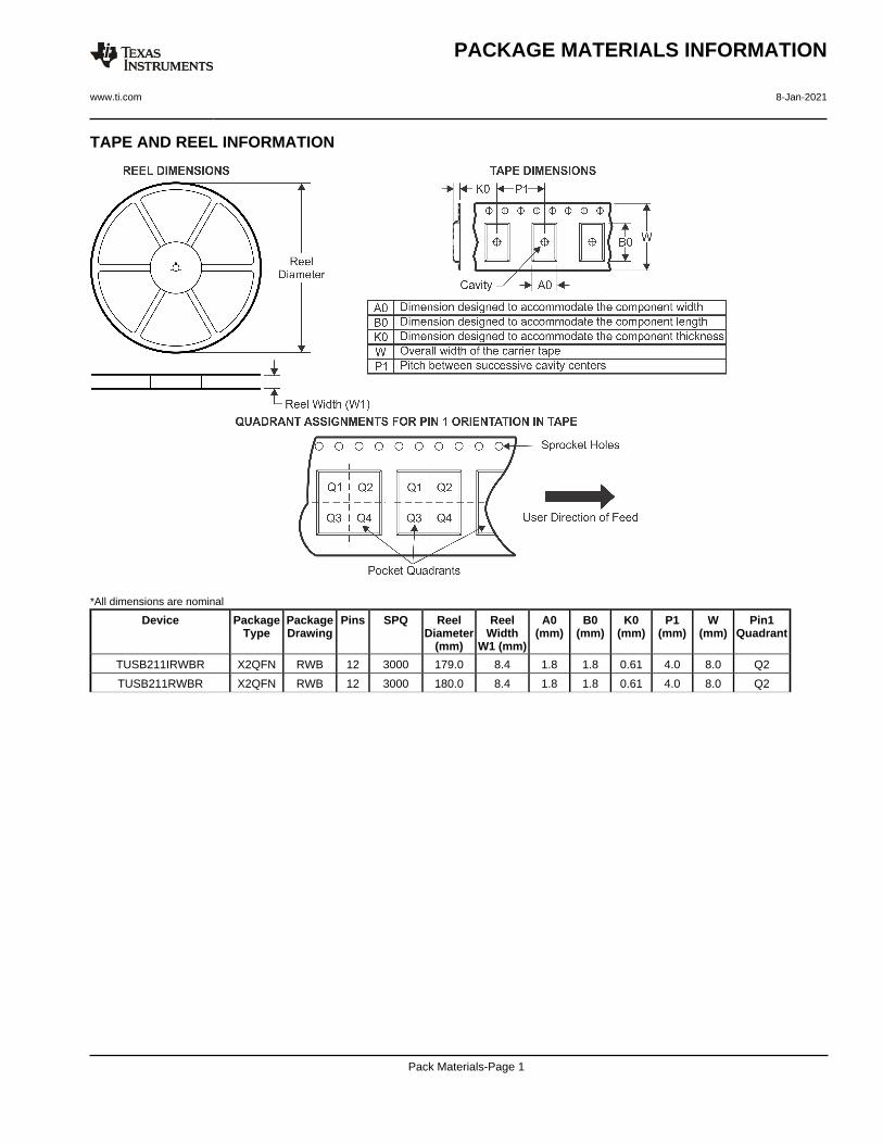
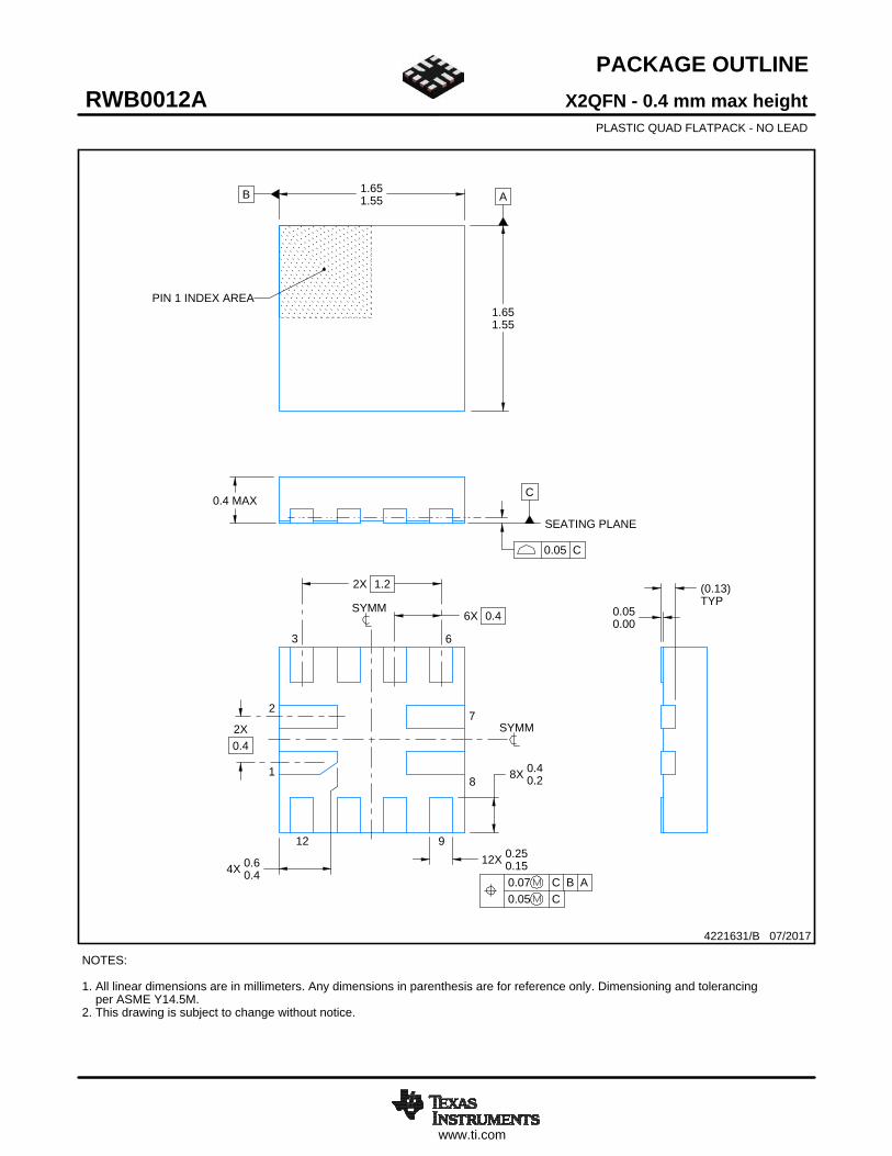
X2QFN - 0.4 mm max heightRWB0012APLASTIC QUAD FLATPACK - NO LEAD
4221631/B 07/2017
PIN 1 INDEX AREA
SEATING PLANE
0.05 C
1
2
3
12
0.07 C B A0.05 C
NOTES: 1. All linear dimensions are in millimeters. Any dimensions in parenthesis are for reference only. Dimensioning and tolerancing per ASME Y14.5M. 2. This drawing is subject to change without notice.
6
7
8
9
SYMM
SYMM
SCALE 6.500
www.ti.com
EXAMPLE BOARD LAYOUT
(R0.05) TYP
0.05 MINALL AROUND
0.05 MAXALL AROUND
12X (0.2)
8X (0.5)
(1.3)
(1.5)2X (0.4)
4X (0.7)
6X (0.4)
X2QFN - 0.4 mm max heightRWB0012APLASTIC QUAD FLATPACK - NO LEAD
4221631/B 07/2017
SYMM
1
27
12
SYMM
LAND PATTERN EXAMPLEEXPOSED METAL SHOWN
SCALE:30X
9
3 6
8
NOTES: (continued) 3. For more information, see Texas Instruments literature number SLUA271 (www.ti.com/lit/slua271).
METAL
SOLDER MASKOPENING
SOLDER MASK DETAILS
NON SOLDER MASKDEFINED
(PREFERRED)
EXPOSED METAL
SOLDER MASKOPENING
METAL UNDERSOLDER MASK
SOLDER MASKDEFINED
EXPOSED METAL
www.ti.com
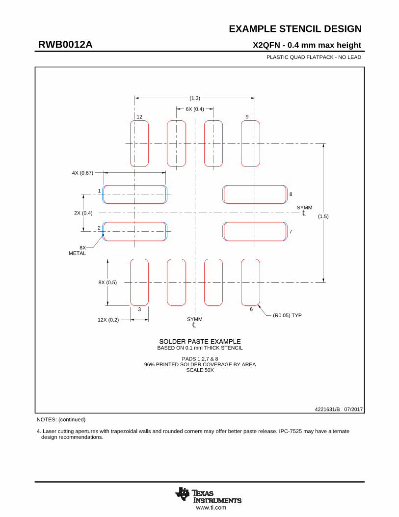
EXAMPLE STENCIL DESIGN
12X (0.2)
8X (0.5)
4X (0.67)
2X (0.4) (1.5)
(1.3)
6X (0.4)
(R0.05) TYP
X2QFN - 0.4 mm max heightRWB0012APLASTIC QUAD FLATPACK - NO LEAD
4221631/B 07/2017
NOTES: (continued) 4. Laser cutting apertures with trapezoidal walls and rounded corners may offer better paste release. IPC-7525 may have alternate design recommendations.
SYMM
SOLDER PASTE EXAMPLEBASED ON 0.1 mm THICK STENCIL
PADS 1,2,7 & 8
96% PRINTED SOLDER COVERAGE BY AREASCALE:50X
1
2
3 6
7
8
912
SYMM
METAL8X
IMPORTANT NOTICE AND DISCLAIMERTI PROVIDES TECHNICAL AND RELIABILITY DATA (INCLUDING DATASHEETS), DESIGN RESOURCES (INCLUDING REFERENCEDESIGNS), APPLICATION OR OTHER DESIGN ADVICE, WEB TOOLS, SAFETY INFORMATION, AND OTHER RESOURCES “AS IS”AND WITH ALL FAULTS, AND DISCLAIMS ALL WARRANTIES, EXPRESS AND IMPLIED, INCLUDING WITHOUT LIMITATION ANYIMPLIED WARRANTIES OF MERCHANTABILITY, FITNESS FOR A PARTICULAR PURPOSE OR NON-INFRINGEMENT OF THIRDPARTY INTELLECTUAL PROPERTY RIGHTS.These resources are intended for skilled developers designing with TI products. You are solely responsible for (1) selecting the appropriateTI products for your application, (2) designing, validating and testing your application, and (3) ensuring your application meets applicablestandards, and any other safety, security, or other requirements. These resources are subject to change without notice. TI grants youpermission to use these resources only for development of an application that uses the TI products described in the resource. Otherreproduction and display of these resources is prohibited. No license is granted to any other TI intellectual property right or to any third partyintellectual property right. TI disclaims responsibility for, and you will fully indemnify TI and its representatives against, any claims, damages,costs, losses, and liabilities arising out of your use of these resources.TI’s products are provided subject to TI’s Terms of Sale (https:www.ti.com/legal/termsofsale.html) or other applicable terms available eitheron ti.com or provided in conjunction with such TI products. TI’s provision of these resources does not expand or otherwise alter TI’sapplicable warranties or warranty disclaimers for TI products.IMPORTANT NOTICE