25
TUSB9261 DEMO Board Guide User's Guide Literature Number: SLLU139A February 2011 – Revised December 2014

TUSB9261 DEMO Board Guide
User's Guide
Literature Number: SLLU139AFebruary 2011–Revised December 2014

Contents
1 TUSB9261 DEMO Board Block Diagram .................................................................................. 42 Component Location ............................................................................................................ 53 12-V DC Jack ....................................................................................................................... 64 Cable Power vs. Self Power................................................................................................... 75 Power Switch....................................................................................................................... 86 3.3-V and 1.1-V Regulator...................................................................................................... 91 Push Button Reset ............................................................................................................... 97 SPI.................................................................................................................................... 108 Crystal or Oscillator Support ............................................................................................... 119 GPIOs/LEDs/PBUTTON ....................................................................................................... 121 GPIO LEDs ........................................................................................................................ 122 PWM LEDs......................................................................................................................... 123 GPIO Push Button .............................................................................................................. 1210 Default GPIO/PWM Configures States ................................................................................... 1311 Troubleshooting Tips for Windows....................................................................................... 141 Step 1 ............................................................................................................................... 152 Step 2 ............................................................................................................................... 1512 TUSB9261 DEMO Board Schematic ...................................................................................... 17Revision History.......................................................................................................................... 20
2 Table of Contents SLLU139A–February 2011–Revised December 2014Submit Documentation Feedback
Copyright © 2011–2014, Texas Instruments Incorporated

www.ti.com
List of Figures1 DEMO Board Block Diagram............................................................................................... 42 Component Location ........................................................................................................ 53 Windows Troubleshooting................................................................................................. 144 Disk Management .......................................................................................................... 155 Primary Partition............................................................................................................ 156 Healthy Disk Status ........................................................................................................ 167 Drive in Windows Explorer ................................................................................................ 16
List of Tables1 Frequency Select Map..................................................................................................... 112 GPIO and PWM Factory Default Settings............................................................................... 133 Link Power Status .......................................................................................................... 13
3SLLU139A–February 2011–Revised December 2014 List of FiguresSubmit Documentation Feedback
Copyright © 2011–2014, Texas Instruments Incorporated

TUSB9261
SLLU139A–February 2011–Revised December 2014
TUSB9261 DEMO Board Block Diagram
Figure 1 represents the block diagram of the TUSB9261 DEMO Board. The board is designed to bepowered from either a 12-V DC wall-wart (not supplied) or via USB cable power.
Figure 1. DEMO Board Block Diagram
4 TUSB9261 DEMO Board Block Diagram SLLU139A–February 2011–Revised December 2014Submit Documentation Feedback
Copyright © 2011–2014, Texas Instruments Incorporated

TUSB9261
SLLU139A–February 2011–Revised December 2014
Component Location
Figure 2 shows the general location of major components on the TUSB9261 DEMO Board.
Figure 2. Component Location
5SLLU139A–February 2011–Revised December 2014 Component LocationSubmit Documentation Feedback
Copyright © 2011–2014, Texas Instruments Incorporated

SLLU139A–February 2011–Revised December 2014
12-V DC Jack
The DEMO Board can operate from a standard DC jack for connecting an external 12-V wall-wart. Thewall-wart should be rated for 12 V with at least a 2-A current rating. The tip of the DC jack has positivepolarity. A wall-wart is not supplied with this reference design demonstration module, leaving it capable ofbus power mode by default. In this mode, only Solid State Drives will work. If other higher current harddrives are to be used a wall-wart will have to be used.
6 12-V DC Jack SLLU139A–February 2011–Revised December 2014Submit Documentation Feedback
Copyright © 2011–2014, Texas Instruments Incorporated

SLLU139A–February 2011–Revised December 2014
Cable Power vs. Self Power
The DEMO Board can be configured to operate off of cable power or use the 12-V wall-wart. To configurethe board to use cable power jumper J4 must have a jumper placed across pins 1 and 2. When configuredfor cable power mode only 5-V and 3.3-V are available at the SATA connector. Therefore only SATAdevices such as SSD drives may operate in this mode.
For self power mode J4 must have a jumper placed across pins 2 and 3. In this mode any SATA devicecan operate since 12 V, 5 V, and 3.3 V are available at the SATA connector.
7SLLU139A–February 2011–Revised December 2014 Cable Power vs. Self PowerSubmit Documentation Feedback
Copyright © 2011–2014, Texas Instruments Incorporated

SLLU139A–February 2011–Revised December 2014
Power Switch
The DEMO Baord uses a TI TPS2561 power switch. This switch serves two purposes. It limits the amountof in-rush current on VBUS and it allows power to the SATA connector to be switched via the TUSB9261.The switch is controlled via GPIO10 from the TUSB9261 and power faults can be monitored by GPIO11.By default the DEMO Board is configured to always apply power to the SATA connector and power faultsare not monitored.
8 Power Switch SLLU139A–February 2011–Revised December 2014Submit Documentation Feedback
Copyright © 2011–2014, Texas Instruments Incorporated

SLLU139A–February 2011–Revised December 2014
3.3-V and 1.1-V Regulator
The DEMO Board utilizes a TI TPS650061 regulator to power the TUSB9261 and associated circuitry.
1 Push Button ResetConnected to the TPS650061 is a push button (SW2) that can be used to reset the TUSB9261 to itsdefault state. When pressed the global reset terminal (GRST#) on the TUSB9261 will be driven low.
9SLLU139A–February 2011–Revised December 2014 3.3-V and 1.1-V RegulatorSubmit Documentation Feedback
Copyright © 2011–2014, Texas Instruments Incorporated
SLLU139A–February 2011–Revised December 2014
SPI
The TUSB9261 supports a SPI interface connected to a SPI flash device. The flash device is used to holdthe firmware for the TUSB9261.
For normal SPI operation a jumper on J13 must be populated. For reprogramming of the SPI flash deviceit may be necessary to temporally remove J13. Refer to the TUSB9260 Flash Burner User Guide(SLLU125) for more information about programming the SPI flash.
10 SPI SLLU139A–February 2011–Revised December 2014Submit Documentation Feedback
Copyright © 2011–2014, Texas Instruments Incorporated

SLLU139A–February 2011–Revised December 2014
Crystal or Oscillator Support
The TUSB9261 DEMO can support either a crystal or oscillator reference clock. By default the board isconfigured to use a 40-MHz crystal. To use an oscillator R23 and R37 need to be populated with a 0-Ωresistor. C17 and C19 need to be de-populated. The crystal or oscillator should be rated for 1.8 V withPPM of ±100 or better. The frequency of the clock is configurable via resistors R10-R13. Table 1 showshow to populate resistors R10-R13 for desired clock frequency.
Table 1. Frequency Select Map
FREQUENCY (MHz) R10 R11 R12 R1340 POP POP
11SLLU139A–February 2011–Revised December 2014 Crystal or Oscillator SupportSubmit Documentation Feedback
Copyright © 2011–2014, Texas Instruments Incorporated

SLLU139A–February 2011–Revised December 2014
GPIOs/LEDs/PBUTTON
1 GPIO LEDsEach GPIO is connected to an LED on the DEMO Board. The LEDs are located along the top side of theboard (D1 – D8). The LEDs are for test purposes and can be used to indicate device operational states.This is firmware dependent.
2 PWM LEDsEach PWM is connected to an LED (D3 and D6) on the DEMO Board. PWM LEDs are for test purposesand can be used to indicate hard drive activity or USB activity. This is firmware dependent.
3 GPIO Push ButtonThere is one GPIO configurable push button (SW1) on the DEMO Board. This push button is connected toGPIO3. This is firmware dependent.
12 GPIOs/LEDs/PBUTTON SLLU139A–February 2011–Revised December 2014Submit Documentation Feedback
Copyright © 2011–2014, Texas Instruments Incorporated

SLLU139A–February 2011–Revised December 2014
Default GPIO/PWM Configures States
Table 2 shows the factory default programmed settings for the GPIO and PWM terminals used on thePDK.
Table 2. GPIO and PWM Factory Default Settings
GPIO LED NO. DEFAULT FUNCTION DESCRIPTION0 D1 SW_HB Software Heartbeat: Flashes to indicate firmware is executing1 D4 PWR_STATE_0 Power State bit 0 - See Table 3
High Speed / Full Speed Suspend: Indicates when USB2 high2 D2 HS_FS_SUSPEND# speed or full speed is in the suspended statePush Button: Input terminal connected to active low push3 PBUTTON# button
4 SELF_PWR Bus or Self-powered indicator input - HIGH when self-powered5 D7 PWR_STATE_1 Power State bit 1 - See Table 3
High Speed / Full Speed Connect: Indicates when a high6 D5 HS_FS_CONNECT# speed or full speed connection is establishedSuperSpeed Connect: Indicates when a SuperSpeed7 D8 SS_CONNECT# connection has been established
8 UART Tx Debug port is not pinned out on the TUSB9261DEMO.9 UART Rx Debug port is not pinned out on the TUSB9261DEMO.
Used to control power to SATA connector via option resistors10 SATA_EN R34 and R35.11 FAULT# Indicates a power fault
PWM LED NO. DEFAULT FUNCTION DESCRIPTIONDisk Activity and Device ON (blink rate varies depending on0 D3 HDD_ACT# USB connection speed)
1 D6 MISC_LED0#
Table 3. Link Power Status
GPIO1 GPIO5 LINK POWER STATUSOff Off U0: ActiveOn Off U1: Idle, fast exitOff On U2: Idle, slow ExitOn On U3: Suspend
13SLLU139A–February 2011–Revised December 2014 Default GPIO/PWM Configures StatesSubmit Documentation Feedback
Copyright © 2011–2014, Texas Instruments Incorporated
SLLU139A–February 2011–Revised December 2014
Troubleshooting Tips for Windows
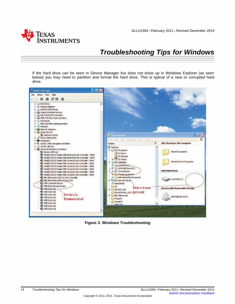
If the hard drive can be seen in Device Manager but does not show up in Windows Explorer (as seenbelow) you may need to partition and format the hard drive. This is typical of a new or corrupted harddrive.
Figure 3. Windows Troubleshooting
14 Troubleshooting Tips for Windows SLLU139A–February 2011–Revised December 2014Submit Documentation Feedback
Copyright © 2011–2014, Texas Instruments Incorporated

www.ti.com Step 1
1 Step 1In the Control Panel, open Administrative Tools → Computer Management. Under Storage, click on DiskManagement.
Figure 4. Disk Management
2 Step 2If you can see the unallocated disk, right click and select New Partition. Follow the Wizard to create aPrimary Partition. Make sure to select the “Perform Quick Format” check box.
Figure 5. Primary Partition
15SLLU139A–February 2011–Revised December 2014 Troubleshooting Tips for WindowsSubmit Documentation Feedback
Copyright © 2011–2014, Texas Instruments Incorporated

Step 2 www.ti.com
Once the disk is properly partitioned and formatted, it will appear as Healthy.
Figure 6. Healthy Disk Status
It will then appear as a drive in Windows Explorer.
Figure 7. Drive in Windows Explorer
16 Troubleshooting Tips for Windows SLLU139A–February 2011–Revised December 2014Submit Documentation Feedback
Copyright © 2011–2014, Texas Instruments Incorporated

SLLU139A–February 2011–Revised December 2014
TUSB9261 DEMO Board Schematic
See following pages.
17SLLU139A–February 2011–Revised December 2014 TUSB9261 DEMO Board SchematicSubmit Documentation Feedback
Copyright © 2011–2014, Texas Instruments Incorporated

5
5
4
4
3
3
2
2
1
1
D D
C C
B B
A A
1. MATCH TO WITHIN 2.5MILS2. 100-ohms DIFFERENTIALIMPEDANCE3. 50-ohms SINGLE-ENDEDIMPEDANCE
1. MATCH TO WITHIN 2.5MILS2. 100-ohms DIFFERENTIALIMPEDANCE3. 50-ohms SINGLE-ENDEDIMPEDANCE
NOTE: TO USE OSCILLATOR IN PLACE OF CRYSTALREMOVE 1M RESISTOR AND 18pF CAPS
ESD PROTECTION
MISC GPIO INDICATORS
SPI ENABLE
SILKSCREEN:GPIO0 (D1): SW_HBGPIO1 (D4): PWR_STATE_0GPIO2 (D2): HS_FS_SUSPEND#GPIO3 (SW1): PBUTTON#GPIO4: SELF_PWRGPIO5 (D7): PWR_STATE_1GPIO6 (D5): HS_FS_CONNECT#GPIO7 (D8): SS_CONNECT#GPIO8: UART_RXGPIO9: UART_TXGPIO10: SATA_ENGPIO11: FAULT#PWM0 (D3): HDD_ACT#PWM1 (D6): MISC_LED0#
* 11 = 40MHz40MHz Crystal
The SATA TX differential pair were swapped tosimplify the EVM board layout. THe 9261firmware provided by TI takes this swap intoaccount.
CAP_SATATXMCAP_SATATXP
CAP_SATARXMCAP_SATARXP
SATATXM
SATARXP
SSRXP
CAP_SSTXM
US_DM
CAP_SSTXPSSTXM
US_DP
SSTXP
SSRXM
VSSOSC
XI
FREQSEL0FREQSEL1
UART_RXUART_TX SPI_SCK
SPI_CE#
USB_R1
USB_R1RTN
CN_VBUS
XO
FUSE_12V
SW_HBPWR_STATE_0HS_FS_SUSPEND#PBUTTON#
PWR_STATE_1HS_FS_CONNECT#SS_CONNECT#
HDD_ACT#MISC_LED0#
SELF_PWR
SW_HB
PWR_STATE_0
PWR_STATE_1
HS_FS_SUSPEND#
HS_FS_CONNECT#
SS_CONNECT#
HDD_ACT#
MISC_LED0#PBUTTON#
SELF_PWR
CAP_SSTXM
CAP_SSTXP
SSRXM
SSRXP
US_DM
US_DP
SATATXP
SATARXM
SPI_SO_J
SPI_SOSPI_SI
VDD_3P3V
BOARD_3P3V
BOARD_1P8V
BOARD_3P3V SATA_5V
BOARD_12V
VDD_1P1V VDDA_3P3V
BOARD_3P3V BOARD_3P3V BOARD_3P3V BOARD_3P3V
VBUS
BOARD_12V
VDD_3P3V
GRST#
SATA_ENFAULT#
Sheet of
SIZE
SCALE: NONE
DWG NO: TUSB9261 DEMO
TUSB9261 DEMO EVM
Saturday, January 29, 2011
C
1 2Sheet of
SIZE
SCALE: NONE
DWG NO: TUSB9261 DEMO
TUSB9261 DEMO EVM
Saturday, January 29, 2011
C
1 2Sheet of
SIZE
SCALE: NONE
DWG NO: TUSB9261 DEMO
TUSB9261 DEMO EVM
Saturday, January 29, 2011
C
1 2
R4110R4110
R14
330
R14
330
J2
Conn USB3_B_AKAK4AA009K1MainSuper
J2
Conn USB3_B_AKAK4AA009K1MainSuper
VBUS1
DM2
DP3
GND4
SSTXN5
SSTXP6
GND7
SSRXN8
SSRXP9
SHIELD010
SHIELD111
D7
LED Green 0805
D7
LED Green 0805
R13 NOPOPR13 NOPOP
R5 NOPOPR5 NOPOP
C2 0.01uFC2 0.01uF
R410K 1%R410K 1%
R9
1M
0402
R9
1M
0402
R19
330
R19
330
U11
TPD2EUSB30
U11
TPD2EUSB30
D+1
D-2 GND
3
R4010R4010
R16
330
R16
330
TUSB9261PVP
U5
TUSB9261PVP
U5
PWM02
PWM13
GRSTZ4
UART_RX_GPIO85
UART_TX_GPIO96
GPIO08
GPIO19
GPIO210
GPIO311
GPIO413
GPIO514
GPIO615
GPIO716
SPI_CS021
SPI_CS1_GPIO1022
SPI_CS2_GPIO1123
FREQSEL030
FREQSEL131
XI52
VSSOSC53 XO54
SATA_TXM56
SATA_TXP57
SATA_RXM59
SATA_RXP60
SPI_SCLK17
SPI_DATA_OUT18
SPI_DATA_IN20
JTAG_TCK25JTAG_TDI26JTAG_TDO27JTAG_TMS28JTAG_TRSTZ29
USB_VBUS50
USB_DM35
USB_DP36
NC
13
7
USB_R138
USB_R1RTN39
USB_SSTXM42
USB_SSTXP43
USB_SSRXM45
USB_SSRXP46
VD
DA
33
62
VD
DA
33
48
VD
D1
VD
DS
HV
7
VD
D1
2
VD
D1
9
VD
DS
HV
24
VD
D3
2
NC
24
4
NC
35
8
VD
DA
33
40
VD
D4
1
VD
D3
35
1
NC
46
4
VD
D3
3
VS
S6
5
VD
D4
7
VD
D5
5
VD
D4
9
VD
D6
1
VD
D6
3
VD
DA
33
34
+ C10220uF
+ C10220uF
R38
NOPOP
R38
NOPOP
R37 NOPOPR37 NOPOP
C19
18pF
C19
18pF
C16
.001uF
C16
.001uF
R8 NOPOPR8 NOPOP
R25
10K
R25
10K
C17
18pF
C17
18pF
R690.9K 1%R690.9K 1%
D2
LED Green 0805
D2
LED Green 0805
C6 0.01uFC6 0.01uF
R12 4.7kR12 4.7k
CN1
10031569-001LF
CN1
10031569-001LF
GNDS1
A+S2
A-S3
GNDS4
B-S5
B+S6
GNDS7
V33P1
V33P2
V33P3
GNDP4
GNDP5
GNDP6
V5P7
V5P8
V5P9
GNDP10
DAS/DSSP11
GNDP12
V12P13
V12P14
V12P15
R22
330
R22
330
F1
PTC FUSE
F1
PTC FUSE
J13
HDR2X1 M .1
J13
HDR2X1 M .1
1 2
R7
10K
1%
R7
10K
1%
D4
LED Green 0805
D4
LED Green 0805
R4210R4210
R20
330
R20
330
D5
LED Green 0805
D5
LED Green 0805
XY1
X OR Y
XY1
X OR Y
XO1
GND2
VCC4
XI3
D3
LED Green 0805
D3
LED Green 0805
N.O.
SW1PB_SWITCH
N.O.
SW1PB_SWITCH
12
43
C15
.1uF
C15
.1uF
D1
LED Green 0805
D1
LED Green 0805
R23 NOPOPR23 NOPOP
R21
330
R21
330
C8
22uF
C8
22uF
R11 NOPOPR11 NOPOP
C45
1uF
C45
1uF
C140.1uF C140.1uF
C7 0.01uFC7 0.01uF
D8
LED Green 0805
D8
LED Green 0805
D6
LED Green 0805
D6
LED Green 0805
U10
TPD2EUSB30
U10
TPD2EUSB30
D+1
D-2 GND
3
U12
TPD2EUSB30
U12
TPD2EUSB30
D+1
D-2 GND
3
+ C12220uF
+ C12220uF
R24
3.65K
R24
3.65K
C2018pFC2018pF
U2
Pm25LV512A
SOIC_8S
U2
Pm25LV512A
SOIC_8S
CE#1
SO2
WP#3
GND4
SI5SCK6HOLD#7VCC8
C18
0.1uF
C18
0.1uF
C11
0.1uF
C11
0.1uF
R10 4.7KR10 4.7K
C130.1uF C130.1uF
C1 0.01uFC1 0.01uF
R3
4.7K
R3
4.7K
R18
330
R18
330
R2
4.7K
R2
4.7K
J1
NOPOP
J1
NOPOP
123
R15
330
R15
330R17
4.7K
R17
4.7K
www.ti.com
18 TUSB9261 DEMO Board Schematic SLLU139A–February 2011–Revised December 2014Submit Documentation Feedback
Copyright © 2011–2014, Texas Instruments Incorporated

5
5
4
4
3
3
2
2
1
1
D D
C C
B B
A A
NOTE: USE LOW ESR CAP
NOTE: USE LOW ESR CAP
5V REGULATOR
STAR GROUND AGND TO GND
3.3V, 1.8V AND 1.1V REGULATOR
POWER SWITCH
VBUS SELECT
TUSB9261 DECOUPLING
CABLE POWERED
SELF POWERED
BOOT PH
VSENSE
ILIM1
SW_1.1VFB_DCDC
MODE
TRSTMR#
BOARD_12VREG_5V
BOARD_1P8V
VDD_1P1V
VDD_1P1V
USB2_1P1V
VDDA_1P8V
VDD_3P3VBOARD_3P3V
VDDA_3P3V
SOURCE_5VREG_5V VBUS
SOURCE_5V
BOARD_3P3V
BOARD_3P3V
BOARD_5V SATA_5V
VDD_1P1V
BOARD_1P8V
BOARD_3P3V
BOARD_5V
AA
A
A
A
SATA_ENFAULT#
GRST#
Sheet of
SIZE
SCALE: NONE
DWG NO: POWER
TUSB9261 DEMO EVM
Thursday, August 26, 2010
C
2 2Sheet of
SIZE
SCALE: NONE
DWG NO: POWER
TUSB9261 DEMO EVM
Thursday, August 26, 2010
C
2 2Sheet of
SIZE
SCALE: NONE
DWG NO: POWER
TUSB9261 DEMO EVM
Thursday, August 26, 2010
C
2 2
C3222uFC3222uF
C54
0.1uF
C54
0.1uF
R35
4.7K
R35
4.7K
C23
0.01uF
C23
0.01uF
C59
0.01uF
C59
0.01uF
C26
0.1uF
C26
0.1uF
C37
0.1uF
C37
0.1uFC3322uFC3322uF
R33
10K
0402
5%
R33
10K
0402
5%
T
S
J3
2.1mm x 5.5mm
T
S
J3
2.1mm x 5.5mm
1
23
C67
0.1uF
C67
0.1uF
U4
TPS650061
U4
TPS650061
VINDCDC8
EN_DCDC10
MODE9
VINLDO115
EN_LDO13
VINLDO218
EN_LDO24
PGND6
AGND12
PG#5
SW7
FB_DCDC11
VLDO114
VLDO217
FB_LDO113
FB_LDO216
RSTSNS19
RST#20MR#
1TRST
2
PWR_PAD21
FB2
220 @ 100MHZ
FB2
220 @ 100MHZ
+ C30
1000uF
+ C30
1000uF
R27
3.16K
1%
R27
3.16K
1%
C38
0.01uF
C38
0.01uF
FB1
220 @ 100MHZ
FB1
220 @ 100MHZ
R30
400K
0402
1%
R30
400K
0402
1%
C61
1uF
C61
1uF
R34NOPOPR34NOPOP
J4
HDR
J4
HDR
123
C43
0.1uF
C43
0.1uF
C58
0.1uF
C58
0.1uF
C25
1uF
C25
1uF
C72
30pF
C72
30pF
C6222uFC6222uF
R26
10K
1%
R26
10K
1%
R39
4.7K0402
R39
4.7K0402
C36
0.1uF
C36
0.1uF
L2
2.2uH
L2
2.2uH
C22
0.01uF
C22
0.01uF
C42
0.01uF
C42
0.01uF
C6422uFC6422uF
C28
0.1uF
C28
0.1uF
C6322uFC6322uF
C31
0.1uF
C31
0.1uF
C4622uFC4622uF
D12
MBRS540T3
D12
MBRS540T3
C40
0.1uF
C40
0.1uF
C35
0.1uF
C35
0.1uF
C6022uFC6022uF
R31475K
04021%
R31475K
04021%
FB4
220 @ 100MHZ
FB4
220 @ 100MHZ
C2422uFC2422uF
C29
0.01uF
C29
0.01uF
C69
0.1uF
C69
0.1uF
C66
0.1uF
C66
0.1uF
C39
0.1uF
C39
0.1uF
FB5
220 @ 100MHZ
FB5
220 @ 100MHZ
C34
1uF
C34
1uF
C5722uFC5722uF
C68
0.1uF
C68
0.1uF
L1
15uH
L1
15uH
C27
0.1uF
C27
0.1uF
U7
TPS2560DRC
U7
TPS2560DRC
GND1
IN2
IN3
EN14
EN25
FAULT2Z6
ILIM7
OUT28
OUT19
FAULT1Z10
PAD11
+ C21220uF
+ C21220uF
C44
0.1uF
C44
0.1uF
R36
27.4K
0402
5%
R36
27.4K
0402
5%
N.O.
SW2PB_SWITCH
N.O.
SW2PB_SWITCH
12
43
U3
TPS5450
U3
TPS5450
BOOT1
NC2
NC_3
VSENSE4
ENA5GND6VIN7PH8
GN
D9
C41
0.1uF
C41
0.1uF
R32
4.7K04025%
R32
4.7K04025%
www.ti.com
19SLLU139A–February 2011–Revised December 2014 TUSB9261 DEMO Board SchematicSubmit Documentation Feedback
Copyright © 2011–2014, Texas Instruments Incorporated

Revision History www.ti.com
Revision History
Changes from Original (February 2011) to A Revision .................................................................................................. Page
• Changed text in Chapter 8 From: "By default the board is configured to use a 25-MHz crystal" To: "By default the board isconfigured to use a 40-MHz crystal" .................................................................................................. 11
• Deleted Frequencies 20 - 30 from Table 1 .......................................................................................... 11
NOTE: Page numbers for previous revisions may differ from page numbers in the current version.
20 Revision History SLLU139A–February 2011–Revised December 2014Submit Documentation Feedback
Copyright © 2011–2014, Texas Instruments Incorporated

STANDARD TERMS AND CONDITIONS FOR EVALUATION MODULES1. Delivery: TI delivers TI evaluation boards, kits, or modules, including any accompanying demonstration software, components, or
documentation (collectively, an “EVM” or “EVMs”) to the User (“User”) in accordance with the terms and conditions set forth herein.Acceptance of the EVM is expressly subject to the following terms and conditions.1.1 EVMs are intended solely for product or software developers for use in a research and development setting to facilitate feasibility
evaluation, experimentation, or scientific analysis of TI semiconductors products. EVMs have no direct function and are notfinished products. EVMs shall not be directly or indirectly assembled as a part or subassembly in any finished product. Forclarification, any software or software tools provided with the EVM (“Software”) shall not be subject to the terms and conditionsset forth herein but rather shall be subject to the applicable terms and conditions that accompany such Software
1.2 EVMs are not intended for consumer or household use. EVMs may not be sold, sublicensed, leased, rented, loaned, assigned,or otherwise distributed for commercial purposes by Users, in whole or in part, or used in any finished product or productionsystem.
2 Limited Warranty and Related Remedies/Disclaimers:2.1 These terms and conditions do not apply to Software. The warranty, if any, for Software is covered in the applicable Software
License Agreement.2.2 TI warrants that the TI EVM will conform to TI's published specifications for ninety (90) days after the date TI delivers such EVM
to User. Notwithstanding the foregoing, TI shall not be liable for any defects that are caused by neglect, misuse or mistreatmentby an entity other than TI, including improper installation or testing, or for any EVMs that have been altered or modified in anyway by an entity other than TI. Moreover, TI shall not be liable for any defects that result from User's design, specifications orinstructions for such EVMs. Testing and other quality control techniques are used to the extent TI deems necessary or asmandated by government requirements. TI does not test all parameters of each EVM.
2.3 If any EVM fails to conform to the warranty set forth above, TI's sole liability shall be at its option to repair or replace such EVM,or credit User's account for such EVM. TI's liability under this warranty shall be limited to EVMs that are returned during thewarranty period to the address designated by TI and that are determined by TI not to conform to such warranty. If TI elects torepair or replace such EVM, TI shall have a reasonable time to repair such EVM or provide replacements. Repaired EVMs shallbe warranted for the remainder of the original warranty period. Replaced EVMs shall be warranted for a new full ninety (90) daywarranty period.
3 Regulatory Notices:3.1 United States
3.1.1 Notice applicable to EVMs not FCC-Approved:This kit is designed to allow product developers to evaluate electronic components, circuitry, or software associated with the kitto determine whether to incorporate such items in a finished product and software developers to write software applications foruse with the end product. This kit is not a finished product and when assembled may not be resold or otherwise marketed unlessall required FCC equipment authorizations are first obtained. Operation is subject to the condition that this product not causeharmful interference to licensed radio stations and that this product accept harmful interference. Unless the assembled kit isdesigned to operate under part 15, part 18 or part 95 of this chapter, the operator of the kit must operate under the authority ofan FCC license holder or must secure an experimental authorization under part 5 of this chapter.3.1.2 For EVMs annotated as FCC – FEDERAL COMMUNICATIONS COMMISSION Part 15 Compliant:
CAUTIONThis device complies with part 15 of the FCC Rules. Operation is subject to the following two conditions: (1) This device may notcause harmful interference, and (2) this device must accept any interference received, including interference that may causeundesired operation.Changes or modifications not expressly approved by the party responsible for compliance could void the user's authority tooperate the equipment.
FCC Interference Statement for Class A EVM devicesNOTE: This equipment has been tested and found to comply with the limits for a Class A digital device, pursuant to part 15 ofthe FCC Rules. These limits are designed to provide reasonable protection against harmful interference when the equipment isoperated in a commercial environment. This equipment generates, uses, and can radiate radio frequency energy and, if notinstalled and used in accordance with the instruction manual, may cause harmful interference to radio communications.Operation of this equipment in a residential area is likely to cause harmful interference in which case the user will be required tocorrect the interference at his own expense.
SPACER
SPACER
SPACER
SPACER
SPACER
SPACER
SPACER
SPACER

FCC Interference Statement for Class B EVM devicesNOTE: This equipment has been tested and found to comply with the limits for a Class B digital device, pursuant to part 15 ofthe FCC Rules. These limits are designed to provide reasonable protection against harmful interference in a residentialinstallation. This equipment generates, uses and can radiate radio frequency energy and, if not installed and used in accordancewith the instructions, may cause harmful interference to radio communications. However, there is no guarantee that interferencewill not occur in a particular installation. If this equipment does cause harmful interference to radio or television reception, whichcan be determined by turning the equipment off and on, the user is encouraged to try to correct the interference by one or moreof the following measures:
• Reorient or relocate the receiving antenna.• Increase the separation between the equipment and receiver.• Connect the equipment into an outlet on a circuit different from that to which the receiver is connected.• Consult the dealer or an experienced radio/TV technician for help.
3.2 Canada3.2.1 For EVMs issued with an Industry Canada Certificate of Conformance to RSS-210
Concerning EVMs Including Radio Transmitters:This device complies with Industry Canada license-exempt RSS standard(s). Operation is subject to the following two conditions:(1) this device may not cause interference, and (2) this device must accept any interference, including interference that maycause undesired operation of the device.
Concernant les EVMs avec appareils radio:Le présent appareil est conforme aux CNR d'Industrie Canada applicables aux appareils radio exempts de licence. L'exploitationest autorisée aux deux conditions suivantes: (1) l'appareil ne doit pas produire de brouillage, et (2) l'utilisateur de l'appareil doitaccepter tout brouillage radioélectrique subi, même si le brouillage est susceptible d'en compromettre le fonctionnement.
Concerning EVMs Including Detachable Antennas:Under Industry Canada regulations, this radio transmitter may only operate using an antenna of a type and maximum (or lesser)gain approved for the transmitter by Industry Canada. To reduce potential radio interference to other users, the antenna typeand its gain should be so chosen that the equivalent isotropically radiated power (e.i.r.p.) is not more than that necessary forsuccessful communication. This radio transmitter has been approved by Industry Canada to operate with the antenna typeslisted in the user guide with the maximum permissible gain and required antenna impedance for each antenna type indicated.Antenna types not included in this list, having a gain greater than the maximum gain indicated for that type, are strictly prohibitedfor use with this device.
Concernant les EVMs avec antennes détachablesConformément à la réglementation d'Industrie Canada, le présent émetteur radio peut fonctionner avec une antenne d'un type etd'un gain maximal (ou inférieur) approuvé pour l'émetteur par Industrie Canada. Dans le but de réduire les risques de brouillageradioélectrique à l'intention des autres utilisateurs, il faut choisir le type d'antenne et son gain de sorte que la puissance isotroperayonnée équivalente (p.i.r.e.) ne dépasse pas l'intensité nécessaire à l'établissement d'une communication satisfaisante. Leprésent émetteur radio a été approuvé par Industrie Canada pour fonctionner avec les types d'antenne énumérés dans lemanuel d’usage et ayant un gain admissible maximal et l'impédance requise pour chaque type d'antenne. Les types d'antennenon inclus dans cette liste, ou dont le gain est supérieur au gain maximal indiqué, sont strictement interdits pour l'exploitation del'émetteur
3.3 Japan3.3.1 Notice for EVMs delivered in Japan: Please see http://www.tij.co.jp/lsds/ti_ja/general/eStore/notice_01.page 日本国内に
輸入される評価用キット、ボードについては、次のところをご覧ください。http://www.tij.co.jp/lsds/ti_ja/general/eStore/notice_01.page
3.3.2 Notice for Users of EVMs Considered “Radio Frequency Products” in Japan: EVMs entering Japan may not be certifiedby TI as conforming to Technical Regulations of Radio Law of Japan.
If User uses EVMs in Japan, not certified to Technical Regulations of Radio Law of Japan, User is required by Radio Law ofJapan to follow the instructions below with respect to EVMs:1. Use EVMs in a shielded room or any other test facility as defined in the notification #173 issued by Ministry of Internal
Affairs and Communications on March 28, 2006, based on Sub-section 1.1 of Article 6 of the Ministry’s Rule forEnforcement of Radio Law of Japan,
2. Use EVMs only after User obtains the license of Test Radio Station as provided in Radio Law of Japan with respect toEVMs, or
3. Use of EVMs only after User obtains the Technical Regulations Conformity Certification as provided in Radio Law of Japanwith respect to EVMs. Also, do not transfer EVMs, unless User gives the same notice above to the transferee. Please notethat if User does not follow the instructions above, User will be subject to penalties of Radio Law of Japan.
SPACER
SPACER
SPACER
SPACER
SPACER

【無線電波を送信する製品の開発キットをお使いになる際の注意事項】 開発キットの中には技術基準適合証明を受けていないものがあります。 技術適合証明を受けていないもののご使用に際しては、電波法遵守のため、以下のいずれかの措置を取っていただく必要がありますのでご注意ください。1. 電波法施行規則第6条第1項第1号に基づく平成18年3月28日総務省告示第173号で定められた電波暗室等の試験設備でご使用
いただく。2. 実験局の免許を取得後ご使用いただく。3. 技術基準適合証明を取得後ご使用いただく。
なお、本製品は、上記の「ご使用にあたっての注意」を譲渡先、移転先に通知しない限り、譲渡、移転できないものとします。上記を遵守頂けない場合は、電波法の罰則が適用される可能性があることをご留意ください。 日本テキサス・イ
ンスツルメンツ株式会社東京都新宿区西新宿6丁目24番1号西新宿三井ビル
3.3.3 Notice for EVMs for Power Line Communication: Please see http://www.tij.co.jp/lsds/ti_ja/general/eStore/notice_02.page電力線搬送波通信についての開発キットをお使いになる際の注意事項については、次のところをご覧ください。http://www.tij.co.jp/lsds/ti_ja/general/eStore/notice_02.page
SPACER4 EVM Use Restrictions and Warnings:
4.1 EVMS ARE NOT FOR USE IN FUNCTIONAL SAFETY AND/OR SAFETY CRITICAL EVALUATIONS, INCLUDING BUT NOTLIMITED TO EVALUATIONS OF LIFE SUPPORT APPLICATIONS.
4.2 User must read and apply the user guide and other available documentation provided by TI regarding the EVM prior to handlingor using the EVM, including without limitation any warning or restriction notices. The notices contain important safety informationrelated to, for example, temperatures and voltages.
4.3 Safety-Related Warnings and Restrictions:4.3.1 User shall operate the EVM within TI’s recommended specifications and environmental considerations stated in the user
guide, other available documentation provided by TI, and any other applicable requirements and employ reasonable andcustomary safeguards. Exceeding the specified performance ratings and specifications (including but not limited to inputand output voltage, current, power, and environmental ranges) for the EVM may cause personal injury or death, orproperty damage. If there are questions concerning performance ratings and specifications, User should contact a TIfield representative prior to connecting interface electronics including input power and intended loads. Any loads appliedoutside of the specified output range may also result in unintended and/or inaccurate operation and/or possiblepermanent damage to the EVM and/or interface electronics. Please consult the EVM user guide prior to connecting anyload to the EVM output. If there is uncertainty as to the load specification, please contact a TI field representative.During normal operation, even with the inputs and outputs kept within the specified allowable ranges, some circuitcomponents may have elevated case temperatures. These components include but are not limited to linear regulators,switching transistors, pass transistors, current sense resistors, and heat sinks, which can be identified using theinformation in the associated documentation. When working with the EVM, please be aware that the EVM may becomevery warm.
4.3.2 EVMs are intended solely for use by technically qualified, professional electronics experts who are familiar with thedangers and application risks associated with handling electrical mechanical components, systems, and subsystems.User assumes all responsibility and liability for proper and safe handling and use of the EVM by User or its employees,affiliates, contractors or designees. User assumes all responsibility and liability to ensure that any interfaces (electronicand/or mechanical) between the EVM and any human body are designed with suitable isolation and means to safelylimit accessible leakage currents to minimize the risk of electrical shock hazard. User assumes all responsibility andliability for any improper or unsafe handling or use of the EVM by User or its employees, affiliates, contractors ordesignees.
4.4 User assumes all responsibility and liability to determine whether the EVM is subject to any applicable international, federal,state, or local laws and regulations related to User’s handling and use of the EVM and, if applicable, User assumes allresponsibility and liability for compliance in all respects with such laws and regulations. User assumes all responsibility andliability for proper disposal and recycling of the EVM consistent with all applicable international, federal, state, and localrequirements.
5. Accuracy of Information: To the extent TI provides information on the availability and function of EVMs, TI attempts to be as accurateas possible. However, TI does not warrant the accuracy of EVM descriptions, EVM availability or other information on its websites asaccurate, complete, reliable, current, or error-free.
SPACER
SPACER
SPACER
SPACER
SPACER
SPACER

SPACER6. Disclaimers:
6.1 EXCEPT AS SET FORTH ABOVE, EVMS AND ANY WRITTEN DESIGN MATERIALS PROVIDED WITH THE EVM (AND THEDESIGN OF THE EVM ITSELF) ARE PROVIDED "AS IS" AND "WITH ALL FAULTS." TI DISCLAIMS ALL OTHERWARRANTIES, EXPRESS OR IMPLIED, REGARDING SUCH ITEMS, INCLUDING BUT NOT LIMITED TO ANY IMPLIEDWARRANTIES OF MERCHANTABILITY OR FITNESS FOR A PARTICULAR PURPOSE OR NON-INFRINGEMENT OF ANYTHIRD PARTY PATENTS, COPYRIGHTS, TRADE SECRETS OR OTHER INTELLECTUAL PROPERTY RIGHTS.
6.2 EXCEPT FOR THE LIMITED RIGHT TO USE THE EVM SET FORTH HEREIN, NOTHING IN THESE TERMS ANDCONDITIONS SHALL BE CONSTRUED AS GRANTING OR CONFERRING ANY RIGHTS BY LICENSE, PATENT, OR ANYOTHER INDUSTRIAL OR INTELLECTUAL PROPERTY RIGHT OF TI, ITS SUPPLIERS/LICENSORS OR ANY OTHER THIRDPARTY, TO USE THE EVM IN ANY FINISHED END-USER OR READY-TO-USE FINAL PRODUCT, OR FOR ANYINVENTION, DISCOVERY OR IMPROVEMENT MADE, CONCEIVED OR ACQUIRED PRIOR TO OR AFTER DELIVERY OFTHE EVM.
7. USER'S INDEMNITY OBLIGATIONS AND REPRESENTATIONS. USER WILL DEFEND, INDEMNIFY AND HOLD TI, ITSLICENSORS AND THEIR REPRESENTATIVES HARMLESS FROM AND AGAINST ANY AND ALL CLAIMS, DAMAGES, LOSSES,EXPENSES, COSTS AND LIABILITIES (COLLECTIVELY, "CLAIMS") ARISING OUT OF OR IN CONNECTION WITH ANYHANDLING OR USE OF THE EVM THAT IS NOT IN ACCORDANCE WITH THESE TERMS AND CONDITIONS. THIS OBLIGATIONSHALL APPLY WHETHER CLAIMS ARISE UNDER STATUTE, REGULATION, OR THE LAW OF TORT, CONTRACT OR ANYOTHER LEGAL THEORY, AND EVEN IF THE EVM FAILS TO PERFORM AS DESCRIBED OR EXPECTED.
8. Limitations on Damages and Liability:8.1 General Limitations. IN NO EVENT SHALL TI BE LIABLE FOR ANY SPECIAL, COLLATERAL, INDIRECT, PUNITIVE,
INCIDENTAL, CONSEQUENTIAL, OR EXEMPLARY DAMAGES IN CONNECTION WITH OR ARISING OUT OF THESETERMS ANDCONDITIONS OR THE USE OF THE EVMS PROVIDED HEREUNDER, REGARDLESS OF WHETHER TI HASBEEN ADVISED OF THE POSSIBILITY OF SUCH DAMAGES. EXCLUDED DAMAGES INCLUDE, BUT ARE NOT LIMITEDTO, COST OF REMOVAL OR REINSTALLATION, ANCILLARY COSTS TO THE PROCUREMENT OF SUBSTITUTE GOODSOR SERVICES, RETESTING, OUTSIDE COMPUTER TIME, LABOR COSTS, LOSS OF GOODWILL, LOSS OF PROFITS,LOSS OF SAVINGS, LOSS OF USE, LOSS OF DATA, OR BUSINESS INTERRUPTION. NO CLAIM, SUIT OR ACTION SHALLBE BROUGHT AGAINST TI MORE THAN ONE YEAR AFTER THE RELATED CAUSE OF ACTION HAS OCCURRED.
8.2 Specific Limitations. IN NO EVENT SHALL TI'S AGGREGATE LIABILITY FROM ANY WARRANTY OR OTHER OBLIGATIONARISING OUT OF OR IN CONNECTION WITH THESE TERMS AND CONDITIONS, OR ANY USE OF ANY TI EVMPROVIDED HEREUNDER, EXCEED THE TOTAL AMOUNT PAID TO TI FOR THE PARTICULAR UNITS SOLD UNDERTHESE TERMS AND CONDITIONS WITH RESPECT TO WHICH LOSSES OR DAMAGES ARE CLAIMED. THE EXISTENCEOF MORE THAN ONE CLAIM AGAINST THE PARTICULAR UNITS SOLD TO USER UNDER THESE TERMS ANDCONDITIONS SHALL NOT ENLARGE OR EXTEND THIS LIMIT.
9. Return Policy. Except as otherwise provided, TI does not offer any refunds, returns, or exchanges. Furthermore, no return of EVM(s)will be accepted if the package has been opened and no return of the EVM(s) will be accepted if they are damaged or otherwise not ina resalable condition. If User feels it has been incorrectly charged for the EVM(s) it ordered or that delivery violates the applicableorder, User should contact TI. All refunds will be made in full within thirty (30) working days from the return of the components(s),excluding any postage or packaging costs.
10. Governing Law: These terms and conditions shall be governed by and interpreted in accordance with the laws of the State of Texas,without reference to conflict-of-laws principles. User agrees that non-exclusive jurisdiction for any dispute arising out of or relating tothese terms and conditions lies within courts located in the State of Texas and consents to venue in Dallas County, Texas.Notwithstanding the foregoing, any judgment may be enforced in any United States or foreign court, and TI may seek injunctive reliefin any United States or foreign court.
Mailing Address: Texas Instruments, Post Office Box 655303, Dallas, Texas 75265Copyright © 2015, Texas Instruments Incorporated
spacer
IMPORTANT NOTICE
Texas Instruments Incorporated and its subsidiaries (TI) reserve the right to make corrections, enhancements, improvements and otherchanges to its semiconductor products and services per JESD46, latest issue, and to discontinue any product or service per JESD48, latestissue. Buyers should obtain the latest relevant information before placing orders and should verify that such information is current andcomplete. All semiconductor products (also referred to herein as “components”) are sold subject to TI’s terms and conditions of salesupplied at the time of order acknowledgment.TI warrants performance of its components to the specifications applicable at the time of sale, in accordance with the warranty in TI’s termsand conditions of sale of semiconductor products. Testing and other quality control techniques are used to the extent TI deems necessaryto support this warranty. Except where mandated by applicable law, testing of all parameters of each component is not necessarilyperformed.TI assumes no liability for applications assistance or the design of Buyers’ products. Buyers are responsible for their products andapplications using TI components. To minimize the risks associated with Buyers’ products and applications, Buyers should provideadequate design and operating safeguards.TI does not warrant or represent that any license, either express or implied, is granted under any patent right, copyright, mask work right, orother intellectual property right relating to any combination, machine, or process in which TI components or services are used. Informationpublished by TI regarding third-party products or services does not constitute a license to use such products or services or a warranty orendorsement thereof. Use of such information may require a license from a third party under the patents or other intellectual property of thethird party, or a license from TI under the patents or other intellectual property of TI.Reproduction of significant portions of TI information in TI data books or data sheets is permissible only if reproduction is without alterationand is accompanied by all associated warranties, conditions, limitations, and notices. TI is not responsible or liable for such altereddocumentation. Information of third parties may be subject to additional restrictions.Resale of TI components or services with statements different from or beyond the parameters stated by TI for that component or servicevoids all express and any implied warranties for the associated TI component or service and is an unfair and deceptive business practice.TI is not responsible or liable for any such statements.Buyer acknowledges and agrees that it is solely responsible for compliance with all legal, regulatory and safety-related requirementsconcerning its products, and any use of TI components in its applications, notwithstanding any applications-related information or supportthat may be provided by TI. Buyer represents and agrees that it has all the necessary expertise to create and implement safeguards whichanticipate dangerous consequences of failures, monitor failures and their consequences, lessen the likelihood of failures that might causeharm and take appropriate remedial actions. Buyer will fully indemnify TI and its representatives against any damages arising out of the useof any TI components in safety-critical applications.In some cases, TI components may be promoted specifically to facilitate safety-related applications. With such components, TI’s goal is tohelp enable customers to design and create their own end-product solutions that meet applicable functional safety standards andrequirements. Nonetheless, such components are subject to these terms.No TI components are authorized for use in FDA Class III (or similar life-critical medical equipment) unless authorized officers of the partieshave executed a special agreement specifically governing such use.Only those TI components which TI has specifically designated as military grade or “enhanced plastic” are designed and intended for use inmilitary/aerospace applications or environments. Buyer acknowledges and agrees that any military or aerospace use of TI componentswhich have not been so designated is solely at the Buyer's risk, and that Buyer is solely responsible for compliance with all legal andregulatory requirements in connection with such use.TI has specifically designated certain components as meeting ISO/TS16949 requirements, mainly for automotive use. In any case of use ofnon-designated products, TI will not be responsible for any failure to meet ISO/TS16949.
Products ApplicationsAudio www.ti.com/audio Automotive and Transportation www.ti.com/automotiveAmplifiers amplifier.ti.com Communications and Telecom www.ti.com/communicationsData Converters dataconverter.ti.com Computers and Peripherals www.ti.com/computersDLP® Products www.dlp.com Consumer Electronics www.ti.com/consumer-appsDSP dsp.ti.com Energy and Lighting www.ti.com/energyClocks and Timers www.ti.com/clocks Industrial www.ti.com/industrialInterface interface.ti.com Medical www.ti.com/medicalLogic logic.ti.com Security www.ti.com/securityPower Mgmt power.ti.com Space, Avionics and Defense www.ti.com/space-avionics-defenseMicrocontrollers microcontroller.ti.com Video and Imaging www.ti.com/videoRFID www.ti-rfid.comOMAP Applications Processors www.ti.com/omap TI E2E Community e2e.ti.comWireless Connectivity www.ti.com/wirelessconnectivity
Mailing Address: Texas Instruments, Post Office Box 655303, Dallas, Texas 75265Copyright © 2015, Texas Instruments Incorporated


