FEATURES 350 watts peak pulse power per line (tP=8/20μs) Protects two I/O lines with uni-directional Low clamping voltage Working voltage:3.3V Low leakage current Meet MSL 1 requirements RoHS compliant MAIN APPLICATIONS RS-232, RS-422 & RS-485 Servers, notebook, and desktop Cellular handsets and accessories Control & monitoring systems Portable electronics Wireless bus protection Set-top box PROTECTION SOLUTION TO MEET IEC61000-4-2 (ESD) ±15kV (air),±8kV (contact) IEC61000-4-4 (EFT) 40A (5/50ns) IEC61000-4-5 (lightning) 25A (8/20μs) MECHANICAL CHARACTERISTICS SOT-23 package Molding compound flammability rating: UL 94V-0 Weight 8 milligrams (approximate) Quantity per reel: 3,000pcs Reel size: 7 inch Lead finish: lead free Marking code: 3M2 SOT-23 Pin Configuration Page 1 SM03 TVS Diode Array Document ID Issued Date Revised Date Revision Page. AS-3110024 2003/03/08 2012/05/16 D 3
Transcript
FEATURES
350 watts peak pulse power per line (tP=8/20µs)
Protects two I/O lines with uni-directional
Low clamping voltage
Working voltage:3.3V
Low leakage current
Meet MSL 1 requirements
RoHS compliant
MAIN APPLICATIONS
RS-232, RS-422 & RS-485
Servers, notebook, and desktop
Cellular handsets and accessories
Control & monitoring systems
Portable electronics
Wireless bus protection
Set-top box
PROTECTION SOLUTION TO MEET
IEC61000-4-2 (ESD) ±15kV (air),±8kV (contact)
IEC61000-4-4 (EFT) 40A (5/50ns)
IEC61000-4-5 (lightning) 25A (8/20µs)
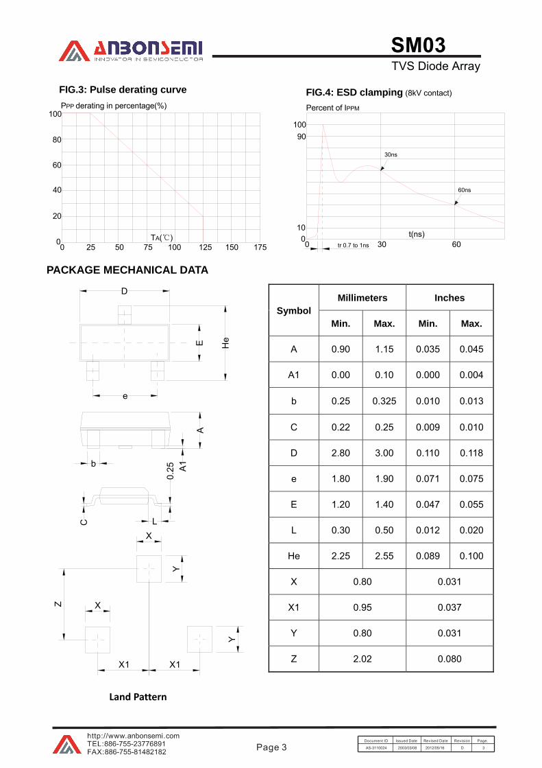
MECHANICAL CHARACTERISTICS
SOT-23 package
Molding compound flammability rating: UL 94V-0
Weight 8 milligrams (approximate)
Quantity per reel: 3,000pcs
Reel size: 7 inch
Lead finish: lead free
Marking code: 3M2
SOT-23
Pin Configuration
Page 1
SM03TVS Diode Array
Document ID Issued Date Revised Date Revision Page.
AS-3110024 2003/03/08 2012/05/16 D 3
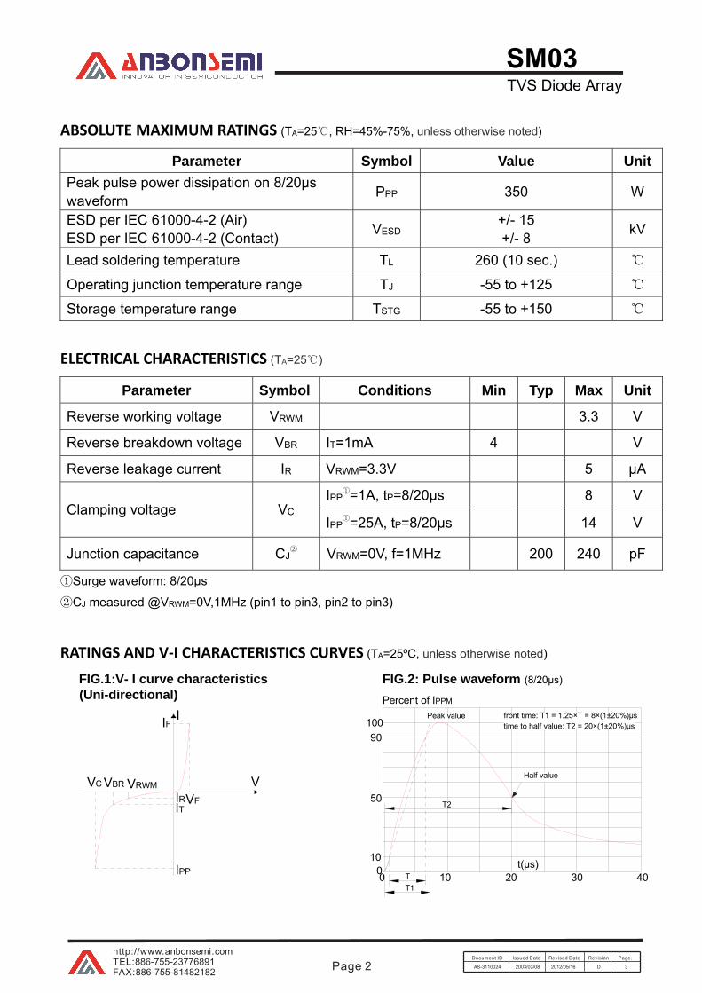
ABSOLUTE MAXIMUM RATINGS (TA=25℃, RH=45%-75%, unless otherwise noted)
Parameter Symbol Value Unit
Peak pulse power dissipation on 8/20μs waveform
PPP 350 W
ESD per IEC 61000-4-2 (Air) ESD per IEC 61000-4-2 (Contact)
VESD +/- 15 +/- 8
kV
Lead soldering temperature TL 260 (10 sec.) ℃
Operating junction temperature range TJ -55 to +125 ℃