Two-dimensional nanomaterials for novel piezotronics andpiezophototronics
P. Lin a, C. Pan a, **, Z.L. Wang a, b, c, *
a CAS Center for Excellence in Nanoscience, Beijing Key Laboratory of Micro-nano Energy and Sensor, Beijing Institute of Nanoenergy and Nanosystems,Chinese Academy of Sciences, Beijing 100083, PR Chinab School of Nanoscience and Technology, University of Chinese Academy of Sciences, Beijing 100049, PR Chinac School of Material Science and Engineering, Georgia Institute of Technology, Atlanta, Georgia 30332, United States
a r t i c l e i n f o
Article history:Received 30 October 2018Received in revised form12 November 2018Accepted 12 November 2018Available online 12 December 2018
Because of the novel properties owing to two-dimensional (2D) confinement, research on 2D nano-materials has become one of the leading topics in condensed matter physics and materials science. Fromthe viewpoint of crystallography, the 2D morphology embodies spontaneous breakdown of three-dimensional symmetry, which means that the inversion symmetry preserved in some bulk materialscan be broken in their corresponding 2D ones, possibly resulting in intrinsic piezoelectric property. Such2D materials in conjunction with their semiconductor properties are good candidates for novel ultrathinpiezotronics and piezophototronics. In one hand, the 2D piezoelectric materials are easy to integrate withthe state-of-the-art semiconductor process and conventional electronic technologies. On the other hand,the possible combination of piezoelectricity with other unusual properties in 2D materials such asferromagnetism or topological insulator may give birth to new physics and innovative devices design fornovel applications. Here, we present an overview of recent breakthroughs in 2D piezotronics and pie-zophototronics, covering from the fundamental principles to their vast applications in energy harvestingand adaptive electronics/optoelectronics. Considering the potential scientific and device developments,we conclude with an in-depth discussion of possible future directions in this active research field.
Piezoelectric effect is unique in a way that couples mechanicalstimulation with electronic output and has found a wide range ofapplications in electromechanical sensors, actuators, and energyconverters since its discovery in 1880. From then on, the mostwidely investigated traditional piezoelectric materials mainlyinclude a mass of inorganic perovskite ceramic crystals (e.g. leadzirconate titanate) and organic polymers (e.g. poly (vinylidenefluoride)) [1e4]. Owing to the intrinsic insulation nature of thesematerials, the coupling research between piezoelectric-inducedpolarization and electronic/optoelectronic processes had conse-quently long been ignored until the discovery of piezoelectricnanogenerators (NGs) using ZnO nanowire arrays byWang in 2006[5]. It verifies that the piezoelectricity can be well preserved in
semiconductors even under the existence of moderate free chargecarriers, opening up a new frontier for microenergy/nanoenergyand self-powered system research [6e9]. By taking advantage ofthe multiple functionalities offered by piezoelectric semi-conductors, Wang proposed the groundbreaking device concepts ofpiezotronics and piezophototronics in 2007 and 2010, respectively[10e14]. From this new physical principle, unprecedented devicetechnologies have been developed with vast potential applicationsin active sensors, human-complementary metal oxide semi-conductor (CMOS) interfacing, logic computation, and nanorobotics[15e19]. Among these piezoelectric semiconductors, the wurtzite-structured ZnO, GaN, and CdS with morphology of one-dimensional (1D) nanowires and nanobelts are the most ofteninvestigated [20e24]. Afterward, the existence of piezoelectric ef-fect in semiconductor materials of other crystal structure has alsobeen demonstrated, which shows the universality of piezoelectricsemiconductors and greatly increases the selectivity of materialsfor piezotronics and piezophototronics. Aftermore than one decadeof intensive efforts, the coupling research between piezopolariza-tion and semiconductor behaviors has logically developed into a
P. Lin et al. / Materials Today Nano 4 (2018) 17e3118
large field of its own and still remains one of the most activeresearch areas for the third-generation semiconductors.
Since the first measurement of single atomic layer graphite(graphene) in 2004, the research on atomically thin crystals hasexploded, and the library of two-dimensional (2D) materials hasgreatly expanded, including conductors, semiconductors withvarying bandgaps (e.g. MoS2 and WSe2), and insulators (e.g. h-BN)[25e28]. Owing to the 2D confinement, these materials displayunique electronic, optical, and mechanical properties that are un-attainable in their bulk counterparts [29e31]. For instance, thedangling bond-free surface of atomic layer allows stacking inte-gration of disparate 2D materials without the constraint of latticematching to create artificial van der Waals (vdWs) heterostructuresor superlattices, giving rise to a new platform for exploring newphysics at the atomic scale [32,33]. In addition, from the point ofcrystallography, the reduced 2D dimensionality embodies sponta-neous breakdown of three-dimensional (3D) symmetry. Conse-quently, some non-piezoelectric bulk materials may becomeintrinsically piezoelectric when thinned to single atomic layer. Thisextends the concept of piezotronics and piezophototronics into anew arena of 2D materials, which may well bring further scientificand device developments. First, compared with the 1D and 3Dmorphology, the crystal structure of 2D materials is simpler. Thisfacilitates the research of structure-property relationship inpiezoelectricity from the first-principles simulation, which couldadvance our fundamental understanding of this old physical effect.Moreover, the possible combination of piezotronic/piezophoto-tronic effects with other exotic properties in 2D materials such asferromagnetism, topological insulators, or quantum spin Hall effectare still far from being fully explored. Furthermore, the 2D mate-rials are easy to fully integrate with the standard semiconductorprocess and well-developed conventional electronic technologies,which may enable the array integration of piezotronics/piezopho-totronics and accelerate their process of practicality.
In this review, we will summarize the recent advances in pie-zotronics/piezophototronics fabricated using novel 2D nano-materials. A brief discussion on the fundamental principles ofpiezotronic and piezophototronic effect is first introduced, followedby the recent studies of piezoelectricity in 2D nanomaterials. Then,theoretical and experimental investigation of 2D piezotronics andpiezophototronics are highlighted, emphasizing their potentialapplications in energy harvesting and adaptive electronics/opto-electronics. In addition, we propose several 2D materials systemsthat can be adopted for piezotronics/piezophototronics. Finally, weoffer our forward-looking perspectives on the future challengesand possible scientific breakthroughs in this burgeoning researchfield.
2. Fundamental principles of piezotronic andpiezophototronic effects
Compared with the conventional electronics (e.g. field-effecttransistors) that rely on the electrostatic coupling between elec-tric field induced by gate voltage and conductive channel, thepiezotronics and piezophototronics represent a totally newsemiconductor-device category through tailoring the interfacialproperty. For piezoelectric semiconductors with moderate chargecarrier density, strain-induced non-mobile piezopolarizationcharges at the vicinity of contact or interface can effectivelymodulate the interfacial energy-band profile and hence the carriertransport across the junction, and this is the basis of piezotroniceffect [34,35]. This novel coupling mode between piezoelectricityand electronic transport has inspired the inventions of manyinnovative electronic devices, such as flexible strain/stress sensors,strain-gated logic units, and nanorobotics [36e38]. The
piezophototronic effect is a result of three-way coupling betweenpiezoelectricity, photonic excitation, and semiconductor transport.By using the strain-induced piezopotential, the electro-opticalprocesses including carrier generation, transport, separation, and/or recombination at the metal-semiconductor Schottky contact orp-n junction can be deliberately controlled [39,40]. Based on thisfundamental principle, the piezophototronic-enhanced optoelec-tronics involving photosensors, light-emitting diodes (LEDs), solarcells, and even the photoelectrochemical devices have been widelydemonstrated [41e47]. In this section, we will take the Schottkycontact and p-n junction as an example to qualitatively illustratethe piezotronic and piezophototronic effects; more detailed nu-merical simulations can be found in other papers [48e52]. ForSchottky contact formed by n-type piezoelectric semiconductorand metal, strain-induced negative piezoelectric polarizationcharges at the interface will further deplete the major electroncarriers in a semiconductor, leading to increased interfacialSchottky barrier height (SBH) and thus the upward bending ofenergy band (Fig. 1a). Alternatively, the positive piezoelectric po-larization charges can attract the free electrons, consequently thebarrier interface becomes less depleted and energy-band bendsdownward (Fig. 1b). It is worth mentioning that because of theultra-high concentration of electrons in metal, the impact ofpiezoelectric potential on metal side could be ignored. Neverthe-less, for p-n heterojunction formed by p-type non-piezoelectricsemiconductor and n-type piezoelectric semiconductor withsimilar and moderate doping concentration, the interfacial piezo-polarization charges can influence the band tilting in both mate-rials. Generally, the strain-induced negative polarization chargeslead to upward bending of interfacial energy bands; therefore, thedepletion width in n- and p-type semiconductor increases anddecreases, respectively (Fig. 1c). In this case, the whole depletionregion shifts toward the n-type side. Instead, the positive polari-zation charges decrease the depletion width in n-type semi-conductor and the whole depletion region shifts toward the p-typeside (Fig. 1d). Moreover, if the density of positive piezopolarizationcharges are so large that it completely inverts the band tilting di-rection at the n-type side, the local deformation of band structurewill create a channel for trapping electrons. For LEDs, the presenceof such electron traps at the interface will increase the recombi-nation possibility of electron-hole pairs, leading to enhancedelectro-optical conversion efficiency [16,53]. In brief, the piezo-tronic and piezophototronic devices are fabricated by using pie-zopotential as a ‘gate’ to modulate the electronic and optoelectronicprocess in semiconductor devices. This interdisciplinary field notonly brings new physics to classic semiconductor theory but alsoopens up a new route to the artificial design of semiconductorinterface with mechanical stimulation for enhanced electronics/optoelectronics and other novel applications.
3. Piezoelectricity in 2D nanomaterials
With the advance of materials synthesis at the molecular level,the piezoelectricity in novel 2D materials is attracting more andmore attention [54,55]. Based on crystallography, it is well knownthat all non-centrosymmetric point groups (except the cubic class432) show piezoelectric effect. Compared with their bulk coun-terparts, the origin of piezoelectricity in novel 2D materials couldbe generally separated into three distinct categories. First, theconventional 3D piezoelectric materials still preserve the piezo-electricity when thinning down to several nanometers, such as thehexagonal CdS and ZnO. Besides, the piezoelectric effect is expectedto be largely enhanced at the nano/atomic scale. Vertical piezo-electric coefficient (d33) up to 33 pm�V�1 was determined for thechemical vapor deposition (CVD)esynthesized CdS ultrathin film
Fig. 1. Schematic for illustrating the modulation of interfacial energy-band profiles at the Schottky contact and p-n heterojunction with piezoelectric potential. The black dotted linerepresents original energy-band tilting under strain-free condition and zero bias, while the realigned bands affected by the positive and negative piezoelectric charges are denotedwith blue and red solid line, respectively.
P. Lin et al. / Materials Today Nano 4 (2018) 17e31 19
with thickness of 2e3 nm, which is approximately three timeslarger than that of the bulk CdS [56]. Wang et al. reported thesynthesis of ~2 nm ZnO nanosheet, and the corresponding piezo-electric coefficient was evaluated to be ~23.7 pm�V�1 (Fig. 2a and b)[57]. This enhanced piezoelectricity was presumably attributed tothe lower carrier concentration and the change in local polariza-tion. Second, multiple materials which are not piezoelectric in bulkbecome intrinsically piezoelectric in their monolayer form becauseof the loss of centrosymmetry. Early studied 2D piezoelectric ma-terials of this type is the insulating h-BN. Owing to the alternatingarrangement of boron and nitride atoms in the hexagonal vertexsite, the monolayer h-BN was theoretically calculated to be piezo-electric [58]. Because of the insulating property, h-BN is not suitablefor piezotronics/piezophototronics, and therefore, it is not paidenough attention. Afterward, based on the density functional the-ory (DFT) calculation, Reed et al. predicted for the first time thatmany of the semiconducting monolayer hexagonal transition metaldichalcogenides (TMDCs) (MX2, M ¼ Mo, W, etc.; X ¼ S, Se, or Te)are intrinsically piezoelectric [59]. Taking theMoS2 for example, thesymmetry in bulk 2H-MoS2 with D6h point group is reduced to D3h
group when thinned down to monolayer [60]. It can be seen fromthe top-view structure (Fig. 2c) that monolayer MoS2 does not havean inversion center along the in-plane (d11) direction and becomespiezoelectric. When mechanically deformed, the relative displace-ment between Mo4þ and S2� ions gives rise to the emergence ofpiezoelectric polarization charges in the material. In 2014, Wu et al.
reported the experimental observation of piezoelectricity inatomically thin MoS2 through the fabrication of flexible NGs andpiezotronic device (Fig. 2d) [61]. Meanwhile, Zhu et al. quantifiedthe piezoelectric coefficient of MoS2 flakes through a method thatcombines laterally applied electric field and nanoindentation(Fig. 2e) [62]. Inspired by this pioneering work, the study ofpiezoelectricity in 2D materials starts to receive its due attention,and the exploration of novel piezoelectric monolayers springs up[63,64]. Based on the first-principles calculations, Li and Lidemonstrated that several monolayer group-III mono-chalcogenides (MX, M¼ Ga or In, X¼ S or Se) are piezoelectric [65].As in the case of 2H-MoS2 monolayer, the MX monolayers alsobelong to D3h point group, leading to the potential piezoelectricityin them (Fig. 2f). Fei et al. predicted the anisotropic piezoelectriceffect in monolayer group-IV monochalcogenides (MX, M ¼ Sn orGe, X ¼ Se or S), and piezoelectric coefficients of these monolayersare expected to be about one to two orders of magnitude largerthan other frequently used piezoelectric materials (Fig. 2g) [60].Then, another two new phases of monolayer group-IV mono-chalcogenides were predicted by Hu and Dong, and both of themare supposed to exhibit significant piezoelectric properties [66].Gao and Gao calculated the piezoelectric properties of group III-V(GaP, GaAs, GaSb, etc.) buckled honeycomb monolayers and theo-retically predicted that they are all good piezoelectric materials[67]. More recently, an intensive data mining for over 50,000inorganic crystals was carried out by Cheon et al., and 325 potential
Fig. 2. (a) Schematic illustration of the ultrathin ZnO film with wurtzite structure. A piezoelectric field that points along the c-axis when the unit cell of ZnO nanomaterial iscompressed by external force in the z-direction. (b) Atomic force microscopy topography of the ultrathin ZnO film and average amplitude variations vs. applied voltages [57].(c) Monolayer top-view and side-view geometry of 2H-MoS2 [59]. (d) A typical flexible single-layer MoS2 nanogenerator on PET substrate with deposited electrodes at its zigzagedge [61]. (e) Schematic of the experimental setup for quantifying the piezoelectric property of freestanding MoS2 flakes and measured piezoelectric coefficient in one-, two- andthree-layer MoS2 membranes [62]. (f) Structure model of gallium sulfide monolayer viewing from top and side [65]. (g) The typical top and side views of group-IV mono-chalcogenides orthorhombic monolayer and calculated piezoelectric coefficient [60]. (h) Top and side view of the typical 2D group III-V buckled honeycomb monolayer.(i) Schematic of the PFMmeasurements on single-layer graphene adsorbed on the TGZ4 grating substrate and cross-sectional of the piezoresponse along the line on graphene acrossthe grating substrate [69]. (j) Graphical representation of the structure of two defects, D3h and C2v point symmetry, of the graphene that break its inversion symmetry and lead tofinite in-plane piezoelectricity [71]. (k) The relationship between uniaxial strain ε11 and polarization charge in graphene sheet when adsorbing different configuration of C2HF andC4HF [72]. Reproduced with permission from: a, b, c, j, k, American Chemical Society; d, e, f, i, Springer Nature; g, AIP Publishing LLC. PET, polyethylene terephthalate; PFM,piezoresponse force microscopy.
P. Lin et al. / Materials Today Nano 4 (2018) 17e3120
2D piezoelectric monolayers were found [68]. The third origin ofpiezoelectricity in 2D materials is from the artificial surface orstructure modification. A typical piezoelectric material of this typeis the graphene. It is well known that graphene is not intrinsicallypiezoelectric because of its inversion symmetry element. However,through proper artificial manipulation of structure, a non-centrosymmetric characteristic can be introduced, leading to
possible piezoelectricity in it. Owing to the chemical interaction ofcarbon atoms with oxygen atoms of the underlying SiO2 substrate,its symmetry crystal structure is broken, resulting in out-of-planepiezoelectricity in graphene (Fig. 2i) [69]. Moreover, throughintroducing proper structural defects (Fig. 2j) or selective adsorp-tion of chemical molecules (Fig. 2k), finite piezoelectricity in gra-phene can also be achieved [70e73]. The demonstration of strong
P. Lin et al. / Materials Today Nano 4 (2018) 17e31 21
piezoelectric effect in the fundamental limit of thickness makes 2Dmaterials a unique platform for exploring the coupling effect be-tween piezoelectricity and other extraordinary phenomena at theatomic scale. Meanwhile, the predicted numerous piezoelectric 2Dmaterials provide broad selection for the fabrication of novel pie-zotronic and piezophototronic devices.
4. Theoretical studies of piezotronic and piezophototroniceffects in 2D materials
In parallel with the exploration of novel piezoelectric 2D ma-terials, the research on numerical simulations of piezotronic andpiezophototronic effect in 2D materials has also emerged. Lopez-Suarez et al. studied the dynamics of piezoelectric h-BN mono-layer by performing ab-initio calculations and explored their po-tential use in non-linear vibration energy harvesting devices [74].In particular, a 20 nm � 1 nm h-BN monolayer under 0.3%compressive strain was predicted to harvest an electrical power ofup to 0.18 pW from a 5 pN noisy vibration. Layer-dependent NGoutput in MoS2 flakes was theoretically examined by Zhou et al.[75]. Fig. 3a shows schematic illustration of the MoS2 NG and
Fig. 3. (a) Schematic illustration of a three-layer MoS2 NG and corresponding equivalent ciunder 0.5% tensile strain. (c) Energy conversion efficiency of monolayer MoS2 NG under diffeits output voltage as a function of strain. (e) Configuration of NG based on WSe2-MoS2 hetervoltage for MoS2 nanoribbon with different length [77]. Reproduced with permission from
corresponding equivalent circuit. Owing to the antiparallel stackingsequence in bulk MoS2, the piezoelectric axis of each monolayerMoS2 is opposed to its adjacent one [76]. Consequently, MoS2 flakeswith an even number of atomic layers do not exhibit piezoelectricoutput, while for MoS2 flakes with an odd number of layers, thepiezoelectric output voltage and surface piezocharges decreasewith the increase of layer number, as shown in Fig. 3b. Moreimportantly, the single-layer MoS2 NG was predicted to be capableof providing satisfactory output under 1 GHZ because of its smallercapacitance, which is considerably higher than the frequency limitof ZnO nanowireebased NGs (Fig. 3c). This result suggests thepromising application of MoS2 NGs in high-frequency self-poweredsystems. In addition, Yu et al. theoretically proposed a design ofnew mechanoelectric NGs based on the TMDCs p-n junctions andinvestigated the size and doping effect [77]. For MoS2 p-n homo-junctionwith doping impurity density of 1013 cm�2 on both sides, amaximum output voltage of 0.31 V was achieved under 8% strain,indicating significantly enhanced performance over the undopedMoS2 sheet (Fig. 3d). However, for WSe2-MoS2 heterojunction, thecorresponding output voltage is only 0.185 V under 8% strain(Fig. 3e). It suggests that MoS2 homojunction-based NG devices
rcuit. (b) Layer-numberedependent MoS2 NG output voltage and surface piezochargesrent frequency of applied strain [75]. (d) Configuration of MoS2 p-n homojunction andojunction and its evolution of output voltage with strain. (f) Comparison of the output: (aec) and (def), Springer Nature. NG, nanogenerator.
P. Lin et al. / Materials Today Nano 4 (2018) 17e3122
possess better output performance than the TMDCs-based heter-ojunctions. Moreover, the output voltage of MoS2 nanoribbonslightly increases by the order of magnitude of 10�6 V withincreasing length, which indicates that the structure length hasnegligible effect on the NG output voltage, as shown in Fig. 3f. Theseresults not only deepen our knowledge of piezoelectricity at thenanometer or atomic scale but also provide theoretical basis for theconstruction of high-efficiency and ultrathin NGs with the novelpiezoelectric 2D nanomaterials.
Although the monolayer MoS2 is intrinsically piezoelectric, afree-standing MoS2 flat sheet was considered to be enclosed byedge-localized metallic states, which may screen the piezoelec-tricity and prevent the piezoelectric output [78]. Based on the DFTsimulation, Liu et al. theoretically reveal the important role ofmetal-MoS2 interface in preserving the piezoelectric effect in MoS2transistors [79]. When the free-standing MoS2 contacts with ametal electrode, the bonding between metal and the edge atoms inMoS2 can effectively eliminate these metallic states, which sup-presses the screening effect. As shown in Fig. 4b and c, for tran-sistors with Pd-MoS2 interface contact, obvious piezopolarization
Fig. 4. (a) Three MoS2 transistors with different Pd-MoS2 interface contact geometries. ((c) Modulation of the Schottky barrier height of transistors with applied strain [79]. (d) Schethe piezocharges distribution in enclosed-contacted MoS2 transistor. (e) The I-V curves ofzocharges at the MoS2/Pd-MoS2 interface. (f) The electron concentrations in the MoS2 flake ain MoS2 monolayer single Schottky solar cell and the band realignment under tensile/comapplied strains. (i) The comparison of piezophototronic modulation impact on MoS2-, MoSeAIP Publishing LLC; (gei), Elsevier Ltd. DFT, density functional theory.
charges can be induced by applied strain and the SBH is effectivelymodulated. In addition, the modulation impact for different inter-face geometries are similar, indicating that the piezoelectric andpiezotronic effects are both intrinsic properties of MoS2 single layer.This result explains why the piezoelectricity in MoS2 can be theo-retically observed even the existence of metallic edge states andverifies the feasibility of piezotronic-modulation in novel 2D ma-terials. Moreover, as the classical piezotronic theory faces thedifficulty in explaining the mechanism of piezotronic effect for top-and enclosed-contacted MoS2 transistors, Liu et al. further theo-retically demonstrated that the strain-induced piezoelectriccharges exist at MoS2/metal-MoS2 interface, which is on the elec-tronic transport pathway rather than at the edge of MoS2 flake, asshown in Fig. 4d [80]. Therefore, the charge transport characteris-tics in MoS2 can be effectively controlled by the applied strain(Fig. 4e). This study deepens our understanding of piezotronictheory in the novel 2D materials and can serve as an importantguidance for future piezotronics design. Besides the piezoelec-tricity, many semiconducting monolayers have also been demon-strated to possess remarkable optical properties such as direct
b) Polarizations of the transistors in (a) and free-standing MoS2 sheet under strain.matic illustration of the difference between the classical and DFT piezotronic theory onenclosed-contacted transistor under the external applied tensile strains with the pie-long the transport direction at 1V bias [80]. (g) Schematic of the energy-band diagrampressive strains. (h) Open-circuit voltage and maximum output power under various2-, and WSe2-based solar cells [81]. Reproduced with permission from (aec) and (def),
P. Lin et al. / Materials Today Nano 4 (2018) 17e31 23
bandgap and strong absorption of visible light, making thempromising candidate for novel 2D piezophototronics. Zheng et al.theoretically simulated the piezophototronic effect in MoS2monolayer-based single Schottky solar cell, as shown in Fig. 4g [81].The strain-induced piezopolarization charges at the interface caneffectively tune the SBH and hence the performance of solar cells.The calculated open-circuit voltage was increased by 5.8% whenapplying a 1% strain (Fig. 4h). Moreover, it demonstrated that themodulation impact of piezophototronic effect on MoS2 solar cell ishigher than that on MoSe2 and WSe2 solar cells, as presented inFig. 4i. This may be because the MoS2 monolayer possesses thehighest piezoelectric coefficient among them.
5. Piezotronic and piezophototronic applications using 2Dmaterials
Although various monolayer structures are predicted to beintrinsically piezoelectric, only a very limited number of them havebeen experimentally confirmed. Until now, the monolayer MoS2remains the most studied 2D piezoelectric material because of itsmature synthesizing technique and good stability under ambientcondition [82]. In addition, the measured piezoelectric coefficiente11 of MoS2 is comparable to the bulk values of standard piezo-electric crystals such as ZnO or AlN, making it suitable for piezo-tronics and piezophototronics fabrication [62]. In this section, wewill briefly summarize the representative applications that rely onthe piezoelectricity of 2Dmaterials, hoping to provide reference forother potential 2D monolayers and inspire novel device design forthe future piezotronics/piezophototronics.
5.1. NGs for energy harvesting
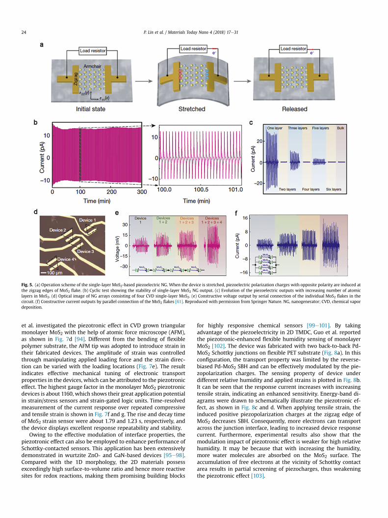
The piezoelectric NGs were first proposed by Wang and Song in2006, which utilizes the piezoelectric effect of nanowires for con-verting tiny mechanical energy into electricity [5]. In essence, theNGs are applications of Maxwell's displacement current in energyand hold great promise for self-powered systems [9,83]. Wu et al.pioneered the work in constructing energy harvester with thepiezoelectric 2D MoS2 flakes [61]. The NG was fabricated bytransferring mechanically exfoliated MoS2 onto flexible poly-ethylene terephthalate (PET) substrate and deposition of Pd elec-trodes at the zigzag edge of MoS2 to form Schottky contacts(Fig. 5a). Periodic stretching and releasing of substrate generatesstable and reproducible alternating piezoelectric outputs inexternal circuit, as displayed in Fig. 5b. Meanwhile, layer-numberdependence of piezoelectric output was also demonstrated in theMoS2 NGs (Fig. 5c), which is consistent with the simulation resultsand measured variation trend of piezoelectric coefficient in MoS2[59,62]. For monolayer MoS2 based NG, the maximum instanta-neous output power at 0.53% strain is about 55.3 fW and the con-version efficiency was estimated as ~5.08%. Meanwhile, theperformance of NG can be further enhanced through array inte-gration, as shown in Fig. 5def.
Besides the layer-dependent piezoelectric output in MoS2 NG,Kim et al. demonstrated the direction-dependent piezoelectric ef-fect in CVD-grown triangular-shaped monolayer MoS2 [84]. Themeasured d11 of MoS2 in the armchair direction is about 3.78 pmV�1, while the piezoelectric coefficient in the zigzag direction isonly 1.38 pm V�1 (Fig. 6b and e). Consequently, under the sameapplied strain of 0.48%, the output voltage of NG with armchairdirection of MoS2 reached up to 20 mV. On the other hand, thegenerated voltage from NG with zigzag direction was less than10mV (Fig. 6c and f). In addition, previous research on piezoelectricZnO nanowire NGs has demonstrated that the piezoelectric prop-erty in semiconductor is closely related with the carrier
concentration [85]. The CVD synthesized 2D materials have beendemonstrated to be host to a wide range of defect types. Based onthis principle, Han et al. further proposed a sulfur (S) vacancypassivation method to reduce the screening of piezopolarizationcharges by free carriers in MoS2 [86]. After defect passivation, thecarrier density in MoS2 decreased from 2.19 � 1012 cm�2 to6.11 � 1011 cm�2. Meanwhile, the obtained piezoelectric coefficientincreased from 3.06 pm�V�1 to 3.73 pm�V�1. The NGs were fabri-cated to further investigate the piezoelectric property change ofdefect-passivated MoS2 monolayer. In the case of output voltage,the S-treated devices show more than 2 times higher than that ofthe pristine MoS2 under the same test condition. It should bementioned that all the above mentioned NGs were fabricated byemploying monolayer TMDC because these materials are predictedto have a greatly reduced or absent piezoelectricity in their multi-layer form. However, Lee et al. demonstrated the reliable piezo-electric property in WSe2 bilayers fabricated via turbostraticstacking [87]. Previous report shows that the CVD-grown WSe2bilayer (b-WSe2) normally has AA0 stacking mode and lose itspiezoelectricity because of the centrosymmetric structure [88]. Butwhen artificially transferring one WSe2 monolayer (m-WSe2) ontoanother, the resulting tb-WSe2 allows another four stacking modesincluding AA, AB, AB0 and A'B [89,90]. Among them, the AA and ABstacked b-WSe2 retain a large piezoelectric coefficient that iscomparable to that of m-WSe2. As the transfer method alleviatesrestriction of geometric relationship between the two separateWSe2 layers, various stacking structures are available, leading to thepossible piezoelectricity in the artificial tb-WSe2. Therefore, pie-zoresponse can be detected in these fabricated tb-WSe2 and themeasured d11 are in the range of 0e1.5 pm V�1. Consequently, a partof the artificially constructed tb-WSe2 can be employed to fabricatepiezoelectric NGs. Moreover, as the bilayer TMDC materials haveoutstanding mechanical properties compared with the monolayerTMDC. The artificial tb-WSe2ebased piezoelectric NGs aredemonstrated to show better mechanical durability. This workprovides a novel approach to artificial manipulation of piezoelec-tricity in multilayer TMDCs and further increases the materialsselectivity for NGs and piezotronics.
5.2. Piezotronic effect enhanced nanosensors
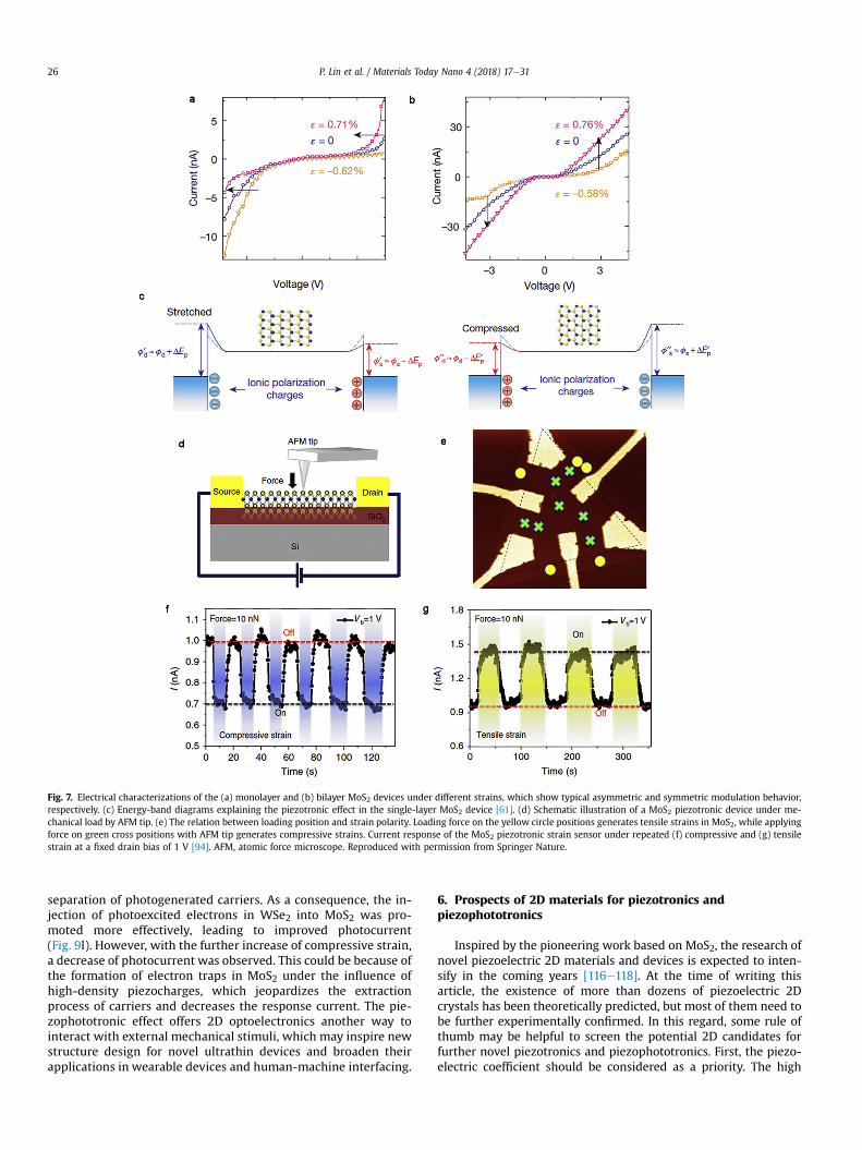
As mentioned in section 2, the piezotronic effect tunes carriertransport process through modulating interfacial barrier height,thus device current changes exponentially with the applied strain.Consequently, compared with the piezoresistive effect, whichmeans a change in bulk electrical resistivity and typically follows alinear relationship with strain, the piezotronic sensors offer amuch-enhanced sensitivity [38,91]. Wu et al. demonstrated thepiezotronic effect in monolayer MoS2 for the first time [61]. Thefabricated metal-semiconductor-metal (MSM) structure consistedof two back-to-back Schottky barriers. For single-layerMoS2 device,it can be seen from Fig. 7a that under positive drain bias, thecurrent-voltage curve shifted leftwards under tensile strain andrightwards with compressive strain, while the opposite trend wasobserved under negative drain bias. This asymmetric modulation isa typical characteristic of the piezotronic effect, which originatesfrom the asymmetric modulation of SBH with strain-induced pie-zopolarization charges at the zigzag edge of MoS2 (Fig. 7c). How-ever, in bilayer MoS2 and bulk devices, the materials lose theirpiezoelectricity, therefore the strain-modulation of current displaysthe same trend under both the positive and negative drain bias(Fig. 7b). The highest gauge factor (the ration between currentchange and strain amplitude) of the monolayer MoS2 piezotronicdevice for strain sensing is ~760, which far exceeds the value ofpiezoresistive MoS2 and graphene-based strain sensors [92,93]. Qi
Fig. 5. (a) Operation scheme of the single-layer MoS2-based piezoelectric NG. When the device is stretched, piezoelectric polarization charges with opposite polarity are induced atthe zigzag edges of MoS2 flake. (b) Cyclic test showing the stability of single-layer MoS2 NG output. (c) Evolution of the piezoelectric outputs with increasing number of atomiclayers in MoS2. (d) Optical image of NG arrays consisting of four CVD single-layer MoS2. (e) Constructive voltage output by serial connection of the individual MoS2 flakes in thecircuit. (f) Constructive current outputs by parallel connection of the MoS2 flakes [61]. Reproduced with permission from Springer Nature. NG, nanogenerator; CVD, chemical vapordeposition.
P. Lin et al. / Materials Today Nano 4 (2018) 17e3124
et al. investigated the piezotronic effect in CVD grown triangularmonolayer MoS2 with the help of atomic force microscope (AFM),as shown in Fig. 7d [94]. Different from the bending of flexiblepolymer substrate, the AFM tip was adopted to introduce strain intheir fabricated devices. The amplitude of strain was controlledthrough manipulating applied loading force and the strain direc-tion can be varied with the loading locations (Fig. 7e). The resultindicates effective mechanical tuning of electronic transportproperties in the devices, which can be attributed to the piezotroniceffect. The highest gauge factor in the monolayer MoS2 piezotronicdevices is about 1160, which shows their great application potentialin strain/stress sensors and strain-gated logic units. Time-resolvedmeasurement of the current response over repeated compressiveand tensile strain is shown in Fig. 7f and g. The rise and decay timeof MoS2 strain sensor were about 1.79 and 1.23 s, respectively, andthe device displays excellent response repeatability and stability.
Owing to the effective modulation of interface properties, thepiezotronic effect can also be employed to enhance performance ofSchottky-contacted sensors. This application has been extensivelydemonstrated in wurtzite ZnO- and GaN-based devices [95e98].Compared with the 1D morphology, the 2D materials possessexceedingly high surface-to-volume ratio and hence more reactivesites for redox reactions, making them promising building blocks
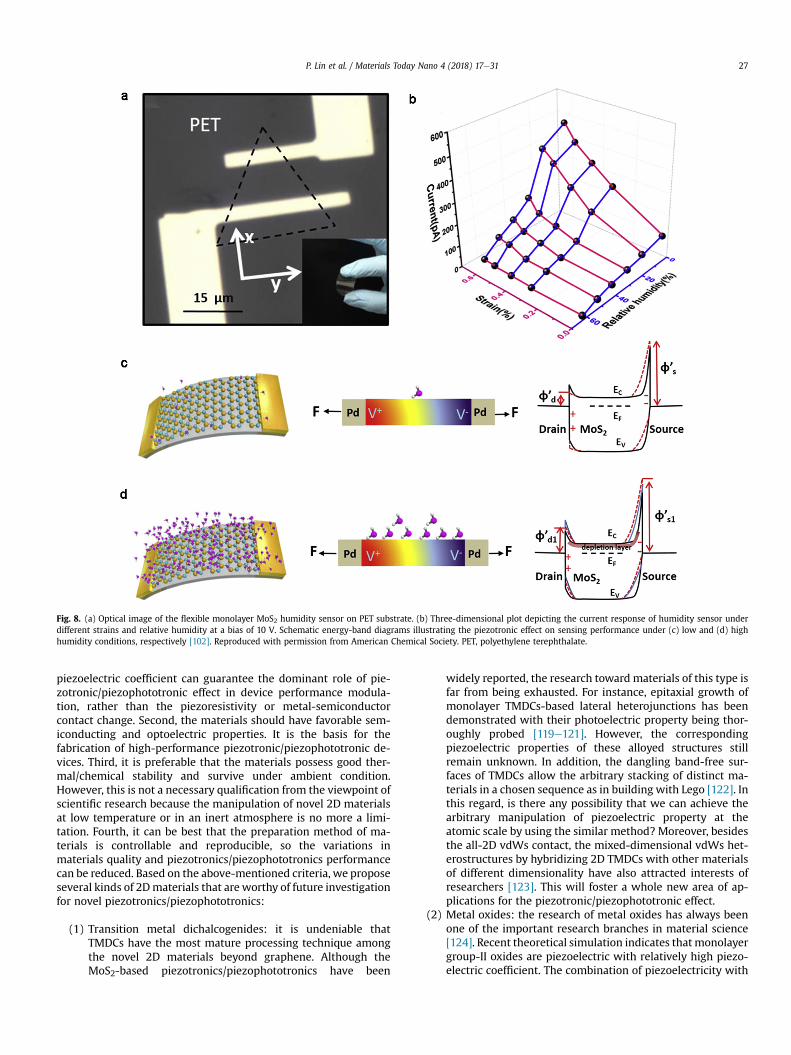
for highly responsive chemical sensors [99e101]. By takingadvantage of the piezoelectricity in 2D TMDC, Guo et al. reportedthe piezotronic-enhanced flexible humidity sensing of monolayerMoS2 [102]. The device was fabricated with two back-to-back Pd-MoS2 Schottky junctions on flexible PET substrate (Fig. 8a). In thisconfiguration, the transport property was limited by the reverse-biased Pd-MoS2 SBH and can be effectively modulated by the pie-zopolarization charges. The sensing property of device underdifferent relative humidity and applied strains is plotted in Fig. 8b.It can be seen that the response current increases with increasingtensile strain, indicating an enhanced sensitivity. Energy-band di-agrams were drawn to schematically illustrate the piezotronic ef-fect, as shown in Fig. 8c and d. When applying tensile strain, theinduced positive piezopolarization charges at the zigzag edge ofMoS2 decreases SBH. Consequently, more electrons can transportacross the junction interface, leading to increased device responsecurrent. Furthermore, experimental results also show that themodulation impact of piezotronic effect is weaker for high relativehumidity. It may be because that with increasing the humidity,more water molecules are absorbed on the MoS2 surface. Theaccumulation of free electrons at the vicinity of Schottky contactarea results in partial screening of piezocharges, thus weakeningthe piezotronic effect [103].
Fig. 6. Lateral electrode configuration to measure the d11 of triangular MoS2 monolayer according to the electric field applied in the direction of (a) armchair and (d) zigzag.Corresponding piezoresponse for the MoS2 in the (b) armchair and (e) zigzag direction, respectively. Voltage outputs of the NGs by applying the same strain along (c) armchair and(f) zigzag directions [84]. Reproduced with permission from Elsevier Ltd. NG, nanogenerator.
P. Lin et al. / Materials Today Nano 4 (2018) 17e31 25
5.3. Piezophototronic effect on 2D materialsebased photodetectors
Photodetectors represent semiconductor devices that canmeasure photon flux or optical power by converting the absorbedphoton energy into electrical current [104]. They are widely usedin various fields, including digital imaging, environmental moni-toring, and astronomy. Generally, three processes are involved inthe operation of photodetectors: (1) carrier generation by incidentlight, (2) carriers transport and/or multiplication if present, (3)extraction of carriers as output current. For Schottky or p-njunctionebased photodetectors, each process is closely relatedwith the interface property and eventually determines the ulti-mate device performance. Thus, the precise tunability overinterface properties is critical to the operation of photodetectors.Recently, particular attention has been paid to the 2D layeredsemiconductors for application in flexible photodetectors due totheir unique electronic, mechanical, and optoelectronic properties[31,62,105,106]. Conventionally, the manipulation of 2Dmaterials-based interface property is achieved by electrostatic gating onhard substrate [107,108]. However, when applying this gate-modulation method to flexible optoelectronics, extra fabricationcomplexity would be introduced including the deposition of high-quality dielectric layer and gate electrode. As plenty of 2Dmonolayers are predicted to be intrinsically piezoelectric, thepiezophototronic effect can be employed as an alternativeapproach to realize such interface regulation. Wu et al. reportedthe first experimental demonstration of piezophototronic effect insingle atomic layer MoS2-based flexible photodetector [109]. Thedevice has similar MSM structure with the above mentionedpiezotronic strain and humidity sensors, as shown in Fig. 9a. Bymodulating the separation and transport of photogenerated car-riers at the MoS2-metal interface, a maximum photoresponsivity
of 2.3 � 104 AW�1 was achieved under 3.4 mW cm�2 633 nm laserillumination, which presents a 26-fold improvement over thereported highest result for monolayer MoS2 phototransistors[110]. Soon afterward, the piezophototronic effect was furtherdemonstrated in other types of MoS2-based p-n junction photo-detectors. A flexible mixed-dimensional heterojunction photode-tector was fabricated with CVD-grown n-MoS2 and p-CuO film onPET substrate [111]. Under a tensile strain of 0.65%, the photo-response current for 532 nm laser can be enhanced 27 timescompared with the strain-free condition and the detectionsensitivity reaches up to 3.27� 108 Jones, as shown in Fig. 9e and f.Furthermore, because of the absence of band discontinuity andlower resistance conductive path than heterojunction, the 2Dhomojunctions are considered to be more preferable for photo-detectors [112,113]. Zhang et al. fabricated a monolayer MoS2lateral p-n junction through selective AuCl3 doping for flexiblephotodiode, and the performance enhancement was also achievedwith piezophototronic effect (Fig. 9g) [114]. When applying a0.51% static tensile strain, the photoresponsivity and detectivity ofdevice reach up to 1161 A W�1 and 1.72 � 1012 Jones, indicating619% and 319% enhancement compared with the strain-free state(Fig. 9h). This performance improvement was attributed to thebroadening of depletion zone in the p-n junction by piezophoto-tronic effect, which benefits the separation and transport processof photogenerated carriers (Fig. 9i). Lin et al. demonstrated thepiezophototronic-enhanced flexible n-MoS2/p-WSe2 all-2D vdWsphotodiode (Fig. 9j) [115]. Under the 1.52 mW cm�2 532 nmillumination and zero bias, an optimized photoresponsivity of~3.4 mA W�1 was achieved when introducing a �0.62%compressive strain. In this case, the compressive strain-inducedpositive piezopolarization charges in MoS2 function as anapplied reverse bias, providing extra driving force for the rapid
Fig. 7. Electrical characterizations of the (a) monolayer and (b) bilayer MoS2 devices under different strains, which show typical asymmetric and symmetric modulation behavior,respectively. (c) Energy-band diagrams explaining the piezotronic effect in the single-layer MoS2 device [61]. (d) Schematic illustration of a MoS2 piezotronic device under me-chanical load by AFM tip. (e) The relation between loading position and strain polarity. Loading force on the yellow circle positions generates tensile strains in MoS2, while applyingforce on green cross positions with AFM tip generates compressive strains. Current response of the MoS2 piezotronic strain sensor under repeated (f) compressive and (g) tensilestrain at a fixed drain bias of 1 V [94]. AFM, atomic force microscope. Reproduced with permission from Springer Nature.
P. Lin et al. / Materials Today Nano 4 (2018) 17e3126
separation of photogenerated carriers. As a consequence, the in-jection of photoexcited electrons in WSe2 into MoS2 was pro-moted more effectively, leading to improved photocurrent(Fig. 9l). However, with the further increase of compressive strain,a decrease of photocurrent was observed. This could be because ofthe formation of electron traps in MoS2 under the influence ofhigh-density piezocharges, which jeopardizes the extractionprocess of carriers and decreases the response current. The pie-zophototronic effect offers 2D optoelectronics another way tointeract with external mechanical stimuli, which may inspire newstructure design for novel ultrathin devices and broaden theirapplications in wearable devices and human-machine interfacing.
6. Prospects of 2D materials for piezotronics andpiezophototronics
Inspired by the pioneering work based on MoS2, the research ofnovel piezoelectric 2D materials and devices is expected to inten-sify in the coming years [116e118]. At the time of writing thisarticle, the existence of more than dozens of piezoelectric 2Dcrystals has been theoretically predicted, but most of them need tobe further experimentally confirmed. In this regard, some rule ofthumb may be helpful to screen the potential 2D candidates forfurther novel piezotronics and piezophototronics. First, the piezo-electric coefficient should be considered as a priority. The high
Fig. 8. (a) Optical image of the flexible monolayer MoS2 humidity sensor on PET substrate. (b) Three-dimensional plot depicting the current response of humidity sensor underdifferent strains and relative humidity at a bias of 10 V. Schematic energy-band diagrams illustrating the piezotronic effect on sensing performance under (c) low and (d) highhumidity conditions, respectively [102]. Reproduced with permission from American Chemical Society. PET, polyethylene terephthalate.
P. Lin et al. / Materials Today Nano 4 (2018) 17e31 27
piezoelectric coefficient can guarantee the dominant role of pie-zotronic/piezophototronic effect in device performance modula-tion, rather than the piezoresistivity or metal-semiconductorcontact change. Second, the materials should have favorable sem-iconducting and optoelectric properties. It is the basis for thefabrication of high-performance piezotronic/piezophototronic de-vices. Third, it is preferable that the materials possess good ther-mal/chemical stability and survive under ambient condition.However, this is not a necessary qualification from the viewpoint ofscientific research because the manipulation of novel 2D materialsat low temperature or in an inert atmosphere is no more a limi-tation. Fourth, it can be best that the preparation method of ma-terials is controllable and reproducible, so the variations inmaterials quality and piezotronics/piezophototronics performancecan be reduced. Based on the above-mentioned criteria, we proposeseveral kinds of 2Dmaterials that are worthy of future investigationfor novel piezotronics/piezophototronics:
(1) Transition metal dichalcogenides: it is undeniable thatTMDCs have the most mature processing technique amongthe novel 2D materials beyond graphene. Although theMoS2-based piezotronics/piezophototronics have been
widely reported, the research toward materials of this type isfar from being exhausted. For instance, epitaxial growth ofmonolayer TMDCs-based lateral heterojunctions has beendemonstrated with their photoelectric property being thor-oughly probed [119e121]. However, the correspondingpiezoelectric properties of these alloyed structures stillremain unknown. In addition, the dangling band-free sur-faces of TMDCs allow the arbitrary stacking of distinct ma-terials in a chosen sequence as in building with Lego [122]. Inthis regard, is there any possibility that we can achieve thearbitrary manipulation of piezoelectric property at theatomic scale by using the similar method? Moreover, besidesthe all-2D vdWs contact, the mixed-dimensional vdWs het-erostructures by hybridizing 2D TMDCs with other materialsof different dimensionality have also attracted interests ofresearchers [123]. This will foster a whole new area of ap-plications for the piezotronic/piezophototronic effect.
(2) Metal oxides: the research of metal oxides has always beenone of the important research branches in material science[124]. Recent theoretical simulation indicates that monolayergroup-II oxides are piezoelectric with relatively high piezo-electric coefficient. The combination of piezoelectricity with
Fig. 9. (a) A flexible monolayer MoS2 piezophototronic device with MSM structure. (b) Piezophototronic mapping for photocurrent in the device under different illuminationintensities and mechanical strains. (c) Working mechanism of the piezophototronic modulation process in monolayer MoS2 photodetector [109]. (d) Schematic illustration of theflexible photodetector based on p-CuO/n-MoS2 heterojunction. The strain dependence of (e) photocurrent and (f) detectivity under different illumination power [111]. (g) Schematicof monolayer MoS2 lateral p-n homojunction photodiode. (h) The variation of device photocurrent under different optical power and applied strains. (i) Working mechanism of thepiezophototronic-modulated MoS2 p-n homojunction photodetector [114]. (j) Optical image of the flexible MoS2/WSe2 all-2D van der Waals photodiode. (k) Strain dependence ofphotocurrent in the device under the illumination of 1.52 mW cm�2 light. (l) Energy-band profile change at the junction interface when positive piezocharges are induced in MoS2under compressive strain [115]. MSM, metal-semiconductor-metal. Reproduced with permission from: (aec) and (jel), John Wiley & Sons, Inc.; (def), Royal Society of Chemistry;(gei), IOP Publishing Ltd.
P. Lin et al. / Materials Today Nano 4 (2018) 17e3128
conventional oxide devices may bring novel breakthroughsin device design concepts and applications.
(3) Layered perovskite materials: the perovskites have beenattracting significant attention in recent years for their excel-lent intrinsic optoelectronic properties, such as direct
bandgap, large absorption coefficient, and high carriermobility [125,126]. From the viewpoint of crystallography, theperovskites are intrinsically piezoelectric. It can be sure thatthe piezophototronic effect holds great potential for applica-tions in perovskite-based optoelectronics such as solar cells,
P. Lin et al. / Materials Today Nano 4 (2018) 17e31 29
photodetectors, and light emitters. However, the 2Dperovskitesebased piezophototronics are scarcely reporteduntil now.
(4) Organic 2D crystals: so far, almost all the reported piezo-tronics/piezophototronics are fabricated with inorganic ma-terials. Nevertheless, the recent rise of organic 2D crystalsmay offer a possibility for extending this novel deviceconcept to a new area [127,128]. At present, the piezoelectricproperty of organic 2D semiconductors is still poorly un-derstood. However, considering the extensive applicativeprospect of organic 2D materials in flexible/stretchableelectronics and optoelectronics, this topic is well worth ourexploration. In short, with the synthetic and assembly ad-vances of piezoelectric 2D materials, much work remains tobe done to make the full use of their potential in novel pie-zotronics/piezophototronics.
7. Summary and outlook
After more than 13 years of worldwide intensive efforts, theresearch of piezotronics/piezophototronics has become a signifi-cant study area and attracted researchers from a wide range ofdisciplines, including condensed matter physics, materials science,electrical engineering, chemistry, and even the biology. Piezotronicand piezophototronic effects are inevitable in the third-generationsemiconductors. Owing the 2D confinement and spontaneousbreaking of inversion symmetry, plenty of materials are theoreti-cally predicted to be piezoelectric in their 2D forms. The integrationof piezoelectricity and other intriguing properties in 2D materialsprovide a new platform for the exploration of novel physics at theatomic scale as well as potential device applications. Therefore, it isbelieved that the 2D piezotronics/piezophototronics will be one ofthe important research branches in this emerging field. Althoughthe fundamental principle of piezotronic/piezophototronic effectshave been well established, our understanding on the couplingbehavior between piezoelectricity and semiconductor propertiesstill needs to be enhanced. For instance, most of the previous nu-merical studies on piezotronic/piezophototronic effects are basedon the finite element method. Now the observation of piezoelec-tricity in the fundamental thickness limit allows us to investigatethese effects from the first-principles calculations, which mayprovide a more accurate interpretation of the underlying mecha-nism. So far, varieties of proof-of-concept devices have beendemonstrated by using piezoelectricity in the 2D materials forpotential applications in energy harvesting, ultrathin actuators,adaptive electronics, and optoelectronics. There is no doubt thatoutstanding opportunities for innovation exist in this emergingfield but with the great challenges on the road ahead.
(1) Further study on the piezoelectricity in 2D materials isrequired. On the one hand, more predicted piezoelectric 2Dmaterials need to be validated with experimental methods.In addition, parameters influencing the 2D piezoelectricityshould be identified so that the artificial manipulation ofpiezoelectric property at the atomic scale can be achieved.For example, design of specific piezoelectric structures maybe realized through arbitrary stacking of vdWs monolayersor chemical functionalization of the 2D materials.
(2) From the viewpoint of scientific research, the combination ofpiezoelectricity with other unique properties in 2D materialslooks more promising than ever before. The topologicalinsulating phase, intrinsic ferromagnetism, and quantumspin Hall effect have been demonstrated in 2D crystals[129e132]. It is possible to use the piezotronic effect to
control the quantum or spin transport process, ultimatelyleading to novel device applications or scientific break-throughs in new physics. Now the coupling research amongmechanical strain, piezoelectricity/ferroelectricity, andferromagnetism in novel 2D materials has not yet been re-ported, but we suppose that it is much worthy of intensivestudy.
(3) So far, most of the reported interpretation of piezotronic/piezophototronic effects are normally based on the qualita-tive analysis of energy band. However, from the viewpoint ofapplication, quantitative characterization methods areneeded. It will not only help to distinguish the role of pie-zotronic/piezophototronic effect from other influencing fac-tors but also provide guidelines for the engineering ofpiezoelectric 2D semiconductors.
(4) The growing interest in novel 2D piezotronics/piezophoto-tronics is not only limited to new physics but also to themassive potential for applications because of their easyintegration with the well-developed semiconductor process.Nevertheless, to realize practical application, the same pri-ority should be placed on the stability and durability of de-vices [133]. Further studies in this direction are necessaryand much work remains to be done from the following as-pects, such as the controllability of materials' piezoelectricproperty, the reliability of metal-semiconductor contact un-der strain, the influence of ambient atmosphere and encap-sulation technology, etc.
Overall, the emergence of piezoelectric 2D materials hasexpanded the piezotronics/piezophototronics research dramati-cally and reserved one of the leading topics in the coming years. Bycombing this new device concept with the rising 2D materialssystem, novel devices have been demonstrated with potential ap-plications in energy harvesting, flexible/stretchable electronics,human-machine interfacing, and self-powered systems. Consid-ering the possible breakthroughs in new physics and their massiveapplication potential on industrial scale, more endeavor is stillneeded to explore the full potential of this exciting research field.
Conflict of interest
The authors declared that they have no conflicts of interest tothis work.
Acknowledgments
The authors thank the support from National Natural ScienceFoundation of China (Grant Nos. 51702017, 51432005, 5151101243,and51561145021)and theNationalKeyR&DProject fromMinisterofScience and Technology (2016YFA0202703 and 2016YFA0202704).
References
[1] A.I. Kingon, S. Srinivasan, Nat. Mater. 4 (2005) 233e237.[2] S.R. Khaled, D. Sameoto, S. Evoy, Smart Mater. Struct. 23 (2014), 033001.[3] C. Ribeiro, C.M. Costa, D.M. Correia, J. Nunes-Pereira, J. Oliveira, P. Martins,
R. Gonçalves, V.F. Cardoso, S. Lanceros-M�endez, Nat. Protoc. 13 (2018) 681.[4] S. Horiuchi, Y. Tokura, Nat. Mater. 7 (2008) 357e366.[5] Z.L. Wang, J. Song, Science 312 (2006) 242e246.[6] S. Xu, Y. Qin, C. Xu, Y. Wei, R. Yang, Z.L. Wang, Nat. Nanotechnol. 5 (2010)
366e373.[7] Z.L. Wang, X. Wang, J. Song, J. Liu, Y. Gao, IEEE Pervasive Comput. 7 (2008)
49e55.[8] Y. Hu, Z.L. Wang, Nano Energy 14 (2015) 3e14.[9] X. Wang, Nano Energy 1 (2012) 13e24.
P. Lin et al. / Materials Today Nano 4 (2018) 17e3130
[13] Z.L. Wang, W. Wu, Natl. Sci. Rev. 1 (2014) 62e90.[14] W. Wu, Z.L. Wang, Nat. Rev. Mater. 1 (2016) 16031.[15] W. Wu, X. Wen, Z.L. Wang, Science 340 (2013) 952e957.[16] C. Pan, L. Dong, G. Zhu, S. Niu, R. Yu, Q. Yang, Y. Liu, Z.L. Wang, Nat. Photonics
7 (2013) 752e758.[17] W. Wu, Y. Wei, Z.L. Wang, Adv. Mater. 22 (2010) 4711e4715.[18] W. Wu, Z.L. Wang, Nano Lett. 11 (2011) 2779e2785.[19] J. Nie, G. Hu, L. Li, Y. Zhang, Nano Energy 46 (2018) 423e427.[20] Z.L. Wang, MRS Bull. 37 (2012) 814e827.[21] H. Liu, Q. Hua, R. Yu, Y. Yang, T. Zhang, Y. Zhang, C. Pan, Adv. Funct. Mater. 26
(2016) 5307e5314.[22] Q. Yang, W. Wang, S. Xu, Z.L. Wang, Nano Lett. 11 (2011) 4012e4017.[23] Q. Yang, X. Guo, W. Wang, Y. Zhang, S. Xu, D.H. Lien, Z.L. Wang, ACS Nano 4
(2010) 6285e6291.[24] C. Pan, S. Niu, Y. Ding, L. Dong, R. Yu, Y. Liu, G. Zhu, Z.L. Wang, Nano Lett. 12
(2012) 3302e3307.[25] K.S. Novoselov, A.K. Geim, S.V. Morozov, D. Jiang, Y. Zhang, S.V. Dubonos,
I.V. Grigorieva, A.A. Firsov, Science 306 (2004) 666e669.[26] M. Chhowalla, H.S. Shin, G. Eda, L.-J. Li, K.P. Loh, H. Zhang, Nat. Chem. 5
(2013) 263e275.[27] M. Xu, T. Liang, M. Shi, H. Chen, Chem. Rev. 113 (2013) 3766e3798.[28] G.R. Bhimanapati, Z. Lin, V. Meunier, Y. Jung, J. Cha, S. Das, D. Xiao, Y. Son,
M.S. Strano, V.R. Cooper, L. Liang, S.G. Louie, E. Ringe, W. Zhou, S.S. Kim,R.R. Naik, B.G. Sumpter, H. Terrones, F. Xia, Y. Wang, J. Zhu, D. Akinwande,N. Alem, J.A. Schuller, R.E. Schaak, M. Terrones, J.A. Robinson, ACS Nano 9(2015) 11509e11539.
[29] G. Fiori, F. Bonaccorso, G. Iannaccone, T. Palacios, D. Neumaier, A. Seabaugh,S.K. Banerjee, L. Colombo, Nat. Nanotechnol. 9 (2014) 768e779.
[30] F. Xia, H. Wang, D. Xiao, M. Dubey, A. Ramasubramaniam, Nat. Photonics 8(2014) 899e907.
[31] D. Akinwande, C.J. Brennan, J.S. Bunch, P. Egberts, J.R. Felts, H. Gao, R. Huang,J.-S. Kim, T. Li, Y. Li, K.M. Liechti, N. Lu, H.S. Park, E.J. Reed, P. Wang,B.I. Yakobson, T. Zhang, Y.-W. Zhang, Y. Zhou, Y. Zhu, Extreme Mech. Lett. 13(2017) 42e77.
[32] Y. Liu, N.O. Weiss, X. Duan, H.-C. Cheng, Y. Huang, X. Duan, Nat. Rev. Mater. 1(2016) 16042.
[33] K.S. Novoselov, A. Mishchenko, A. Carvalho, A.H. Castro Neto, Science 353(2016) aac9439.
[34] W. Wu, C. Pan, Y. Zhang, X. Wen, Z.L. Wang, Nano Today 8 (2013) 619e642.[35] C. Du, W. Hu, Z.L. Wang, Adv. Eng. Mater. 20 (2017) 1700760.[36] J. Zhou, Y. Gu, P. Fei, W. Mai, Y. Gao, R. Yang, G. Bao, Z.L. Wang, Nano Lett. 8
(2008) 3035e3040.[37] R. Yu, W. Wu, Y. Ding, Z.L. Wang, ACS Nano 7 (2013) 6403e6409.[38] R. Yu, S. Niu, C. Pan, Z.L. Wang, Nano Energy 14 (2015) 312e339.[39] Z.L. Wang, Adv. Mater. 24 (2012) 4632e4646.[40] P. Lin, X. Yan, F. Li, J. Du, J. Meng, Y. Zhang, Adv. Mater. Interfaces 4 (2016)
1600842.[41] P. Lin, X. Yan, Z. Zhang, Y. Shen, Y. Zhao, Z. Bai, Y. Zhang, ACS Appl. Mater.
Interfaces 5 (2013) 3671e3676.[42] P. Lin, X. Chen, X. Yan, Z. Zhang, H. Yuan, P. Li, Y. Zhao, Y. Zhang, Nano Res 7
(2014) 860e868.[43] L. Zhu, P. Lin, B. Chen, L. Wang, L. Chen, D. Li, Z.L. Wang, Nano Res 11 (2018)
3877e3885.[44] P. Lin, L. Zhu, D. Li, L. Xu, Z.L. Wang, Nanoscale 10 (2018) 14472e14479.[45] C. Pan, M. Chen, R. Yu, Q. Yang, Y. Hu, Y. Zhang, Z.L. Wang, Adv. Mater. 28
(2015) 1535e1552.[46] X. Han, W. Du, R. Yu, C. Pan, Z.L. Wang, Adv. Mater. 27 (2015) 7963e7969.[47] P. Lin, X. Yan, Y. Liu, P. Li, S. Lu, Y. Zhang, Phys. Chem. Chem. Phys. 16 (2014)
26697e26700.[48] Y. Zhang, Y. Liu, Z.L. Wang, Adv. Mater. 23 (2011) 3004e3013.[49] Y. Zhang, Z.L. Wang, Adv. Mater. 24 (2012) 4712e4718.[50] Y. Zhang, Y. Yang, Z.L. Wang, Energy Environ. Sci. 5 (2012) 6850e6856.[51] Y. Liu, S. Niu, Q. Yang, B.D.B. Klein, Y.S. Zhou, Z.L. Wang, Adv. Mater. 26 (2014)
7209e7216.[52] Y. Liu, Y. Zhang, Q. Yang, S. Niu, Z.L. Wang, Nano Energy 14 (2015) 257e275.[53] Q. Yang, Y. Liu, C. Pan, J. Chen, X. Wen, Z.L. Wang, Nano Lett. 13 (2013)
607e613.[54] Z. Jin, S.A. Meguid, Semicond. Sci. Technol. 32 (2017), 043006.[55] R. Hinchet, U. Khan, C. Falconi, S.-W. Kim, Mater. Today 21 (2018) 611e630.[56] X. Wang, X. He, H. Zhu, L. Sun, W. Fu, X. Wang, L.C. Hoong, H. Wang, Q. Zeng,
W. Zhao, J. Wei, Z. Jin, Z. Shen, J. Liu, T. Zhang, Z. Liu, Sci. Adv. 2 (2016)e1600209.
[57] L. Wang, S. Liu, G. Gao, Y. Pang, X. Yin, X. Feng, L. Zhu, Y. Bai, L. Chen, T. Xiao,X. Wang, Y. Qin, Z.L. Wang, ACS Nano 12 (2018) 4903e4908.
[58] K.H. Michel, B. Verberck, Phys. Rev. B 80 (2009) 224301.[59] K.-A.N. Duerloo, M.T. Ong, E.J. Reed, J. Phys. Chem. Lett. 3 (2012) 2871e2876.[60] R. Fei, W. Li, J. Li, L. Yang, Appl. Phys. Lett. 107 (2015) 173104.[61] W. Wu, L. Wang, Y. Li, F. Zhang, L. Lin, S. Niu, D. Chenet, X. Zhang, Y. Hao,
T.F. Heinz, J. Hone, Z.L. Wang, Nature 514 (2014) 470e474.[62] H. Zhu, Y. Wang, J. Xiao, M. Liu, S. Xiong, Z.J. Wong, Z. Ye, Y. Ye, X. Yin,
9885e9891.[64] C. Sevik, D. Çakır, O. Gülseren, F.M. Peeters, J. Phys. Chem. C 120 (2016)
13948e13953.
[65] W. Li, J. Li, Nano Res. 8 (2015) 3796e3802.[66] T. Hu, J. Dong, Phys. Chem. Chem. Phys. 18 (2016) 32514e32520.[67] R. Gao, Y. Gao, Phys. Status Solidi RRL 11 (2017) 1600412.[68] G. Cheon, K.-A.N. Duerloo, A.D. Sendek, C. Porter, Y. Chen, E.J. Reed, Nano Lett.
17 (2017) 1915e1923.[69] G. da Cunha Rodrigues, P. Zelenovskiy, K. Romanyuk, S. Luchkin,
Y. Kopelevich, A. Kholkin, Nat. Commun. 6 (2015) 7572.[70] S. Chandratre, P. Sharma, Appl. Phys. Lett. 100 (2012), 023114.[71] K.E. El-Kelany, P. Carbonni�ere, A. Erba, M. R�erat, J. Phys. Chem. C 119 (2015)
8966e8973.[72] M.T. Ong, K.-A.N. Duerloo, E.J. Reed, J. Phys. Chem. C 117 (2013) 3615e3620.[73] M.T. Ong, E.J. Reed, ACS Nano 6 (2012) 1387e1394.[74] M. Lopez-Suarez, M. Pruneda, G. Abadal, R. Rurali, Nanotechnology 25 (2014)
175401.[75] Y. Zhou, W. Liu, X. Huang, A. Zhang, Y. Zhang, Z.L. Wang, Nano Res 9 (2016)
800e807.[76] J.A. Wilson, A.D. Yoffe, Adv. Phys. 18 (1969) 193e335.[77] S. Yu, K. Eshun, H. Zhu, Q. Li, Sci. Rep. 5 (2015) 12854.[78] M.V. Bollinger, K.W. Jacobsen, J.K. Nørskov, Phys. Rev. B 67 (2003), 085410.[79] W. Liu, A. Zhang, Y. Zhang, Z.L. Wang, Appl. Phys. Lett. 107 (2015), 083105.[80] W. Liu, Y. Zhou, A. Zhang, Y. Zhang, Z.L. Wang, Appl. Phys. Lett. 108 (2016)
181603.[81] D.Q. Zheng, Z. Zhao, R. Huang, J. Nie, L. Li, Y. Zhang, Nano Energy 32 (2017)
448e453.[82] H. Yu, M. Liao, W. Zhao, G. Liu, X.J. Zhou, Z. Wei, X. Xu, K. Liu, Z. Hu, K. Deng,
S. Zhou, J.-A. Shi, L. Gu, C. Shen, T. Zhang, L. Du, L. Xie, J. Zhu, W. Chen,R. Yang, D. Shi, G. Zhang, ACS Nano 11 (2017) 12001e12007.
[83] Z.L. Wang, Mater. Today 20 (2017) 74e82.[84] S.K. Kim, R. Bhatia, T.-H. Kim, D. Seol, J.H. Kim, H. Kim, W. Seung, Y. Kim,
Y.H. Lee, S.-W. Kim, Nano Energy 22 (2016) 483e489.[85] P. Lin, Y. Gu, X. Yan, S. Lu, Z. Zhang, Y. Zhang, Nano Res 9 (2016) 1091e1100.[86] S.A. Han, T.-H. Kim, S.K. Kim, K.H. Lee, H.-J. Park, J.-H. Lee, S.-W. Kim, Adv.
Mater. 30 (2018) 1800342.[87] J.-H. Lee, J.Y. Park, E.B. Cho, T.Y. Kim, S.A. Han, T.-H. Kim, Y. Liu, S.K. Kim,
C.J. Roh, H.-J. Yoon, H. Ryu, W. Seung, J.S. Lee, J. Lee, S.-W. Kim, Adv. Mater. 29(2017) 1606667.
[88] Y. Li, Y. Rao, K.F. Mak, Y. You, S. Wang, C.R. Dean, T.F. Heinz, Nano Lett. 13(2013) 3329e3333.
[90] A.A. Puretzky, L. Liang, X. Li, K. Xiao, B.G. Sumpter, V. Meunier,D.B. Geohegan, ACS Nano 10 (2016) 2736e2744.
[91] X. Wang, Am. Ceram. Soc. Bull. 92 (2013) 18e23.[92] M. Huang, T.A. Pascal, H. Kim, W.A. Goddard, J.R. Greer, Nano Lett. 11 (2011)
1241e1246.[93] S. Manzeli, A. Allain, A. Ghadimi, A. Kis, Nano Lett. 15 (2015) 5330e5335.[94] J. Qi, Y.-W. Lan, A.Z. Stieg, J.-H. Chen, Y.-L. Zhong, L.-J. Li, C.-D. Chen, Y. Zhang,
K.L. Wang, Nat. Commun. 6 (2015) 7430.[95] C. Pan, R. Yu, S. Niu, G. Zhu, Z.L. Wang, ACS Nano 7 (2013) 1803e1810.[96] S. Niu, Y. Hu, X. Wen, Y. Zhou, F. Zhang, L. Lin, S. Wang, Z.L. Wang, Adv. Mater.
25 (2013) 3701e3706.[97] G. Hu, R. Zhou, R. Yu, L. Dong, C. Pan, Z.L. Wang, Nano Res. 7 (2014)
1083e1091.[98] R. Zhou, G. Hu, R. Yu, C. Pan, Z.L. Wang, Nano Energy 12 (2015) 588e596.[99] J. Zhao, N. Li, H. Yu, Z. Wei, M. Liao, P. Chen, S. Wang, D. Shi, Q. Sun, G. Zhang,
Adv. Mater. 29 (2017) 1702076.[100] D.J. Late, Y.-K. Huang, B. Liu, J. Acharya, S.N. Shirodkar, J. Luo, A. Yan,
[101] F.K. Perkins, A.L. Friedman, E. Cobas, P.M. Campbell, G.G. Jernigan, B.T. Jonker,Nano Lett. 13 (2013) 668e673.
[102] J. Guo, R. Wen, Y. Liu, K. Zhang, J. Kou, J. Zhai, Z.L. Wang, ACS Appl. Mater.Interfaces 10 (2018) 8110e8116.
[103] G. Hu, R. Zhou, R. Yu, L. Dong, C. Pan, Z.L. Wang, Nano Res 7 (2014)1083e1091.
[104] C. Xie, C. Mak, X. Tao, F. Yan, Adv. Funct. Mater. 27 (2016) 1603886.[105] X. Duan, C. Wang, A. Pan, R. Yu, X. Duan, Chem. Soc. Rev. 44 (2015)
8859e8876.[106] K.F. Mak, J. Shan, Nat. Photonics 10 (2016) 216e226.[107] S. Parui, L. Pietrobon, D. Ciudad, S. V�elez, X. Sun, F. Casanova, P. Stoliar,
L.E. Hueso, Adv. Funct. Mater. 25 (2015) 2972e2979.[108] D. Jariwala, S.L. Howell, K.-S. Chen, J. Kang, V.K. Sangwan, S.A. Filippone,
R. Turrisi, T.J. Marks, L.J. Lauhon, M.C. Hersam, Nano Lett. 16 (2016) 497e503.[109] W. Wu, L. Wang, R. Yu, Y. Liu, S.-H. Wei, J. Hone, Z.L. Wang, Adv. Mater. 28
(2016) 8463e8468.[110] O. Lopez-Sanchez, D. Lembke, M. Kayci, A. Radenovic, A. Kis, Nat. Nano-
technol. 8 (2013) 497e501.[111] K. Zhang, M. Peng, W. Wu, J. Guo, G. Gao, Y. Liu, J. Kou, R. Wen, Y. Lei, A. Yu,
Y. Zhang, J. Zhai, Z.L. Wang, Mater. Horiz. 4 (2017) 274e280.[112] M.S. Choi, D. Qu, D. Lee, X. Liu, K. Watanabe, T. Taniguchi, W.J. Yoo, ACS Nano
8 (2014) 9332e9340.[113] Y. Zhao, K. Xu, F. Pan, C. Zhou, F. Zhou, Y. Chai, Adv. Funct. Mater. 27 (2016)
1603484.[114] K. Zhang, J. Zhai, Z.L. Wang, 2D Mater. 5 (2018), 035038.[115] P. Lin, L. Zhu, D. Li, L. Xu, C. Pan, Z.Wang, Adv. Funct. Mater. 28 (2018) 1802849.
[120] M.-Y. Li, C.-H. Chen, Y. Shi, L.-J. Li, Mater. Today 19 (2016) 322e335.[121] Y. Son, M.-Y. Li, C.-C. Cheng, K.-H. Wei, P. Liu, Q.H. Wang, L.-J. Li, M.S. Strano,
Nano Lett. 16 (2016) 3571e3577.[122] A.K. Geim, I.V. Grigorieva, Nature 499 (2013) 419e425.[123] F. Xue, L. Chen, J. Chen, J. Liu, L. Wang, M. Chen, Y. Pang, X. Yang, G. Gao,
J. Zhai, Z.L. Wang, Adv. Mater. 28 (2016) 3391e3398.[124] X. Yu, T.J. Marks, A. Facchetti, Nat. Mater. 15 (2016) 383e396.
[125] X. Gong, O. Voznyy, A. Jain, W. Liu, R. Sabatini, Z. Piontkowski, G. Walters,G. Bappi, S. Nokhrin, O. Bushuyev, M. Yuan, R. Comin, D. McCamant,S.O. Kelley, E.H. Sargent, Nat. Mater. 17 (2018) 550e556.
[126] J. Hu, L. Yan, W. You, Adv. Mater. (2018) 1802041, https://doi.org/10.1002/adma.201802041.
[127] F. Yang, S. Cheng, X. Zhang, X. Ren, R. Li, H. Dong, W. Hu, Adv. Mater. 30(2017) 1702415.
[128] S.K. Park, J.H. Kim, S.Y. Park, Adv. Mater. 30 (2018) 1704759.[129] R.R.Q. Freitas, R. Rivelino, F. de Brito Mota, C.M.C. de Castilho, A. Kakanakova-
Georgieva, G.K. Gueorguiev, J. Phys. Chem. C 119 (2015) 23599e23606.[130] L. Kou, Y.Ma, Z. Sun, T. Heine, C. Chen, J. Phys. Chem. Lett. 8 (2017) 1905e1919.[131] C. Gong, L. Li, Z. Li, H. Ji, A. Stern, Y. Xia, T. Cao, W. Bao, C. Wang, Y. Wang,
Z.Q. Qiu, R.J. Cava, S.G. Louie, J. Xia, X. Zhang, Nature 546 (2017) 265e269.[132] X. Qian, J. Liu, L. Fu, J. Li, Science 346 (2014) 1344e1347.[133] Y. Zhang, Y. Yang, Y. Gu, X. Yan, Q. Liao, P. Li, Z. Zhang, Z. Wang, Nano Energy