Page 1
Two-Stage Operational Amplifier Design by Using Direct andIndirect Feedback Compensations
Jiayuan Zhang
Thesis submitted to the Faculty of the
Virginia Polytechnic Institute and State University
in partial fulfillment of the requirements for the degree of
Master of Science
in
Electrical Engineering
Yang Yi (Cindy), Chair
Lingjia Liu
Xiaoting Jia
May 11, 2021
Blacksburg, Virginia
Keywords: Op-Amp, CMOS, Miller Compensation, etc.
Copyright 2021, Jiayuan Zhang
Page 2
Two-Stage Operational Amplifier Design by Using Direct and Indi-rect Feedback Compensations
Jiayuan Zhang
(ABSTRACT)
This paper states the stability requirements of the amplifier system, and then presents, and
summarizes, the classic two stage CMOS Op-Amp design by employing several popular fre-
quency compensation techniques including traditional Miller compensation, nulling resistor,
voltage buffer, and current buffer. The advantages and disadvantages of all these compen-
sation strategies are evaluated based on a standard performance which has a 70dB DC gain,
a 60◦ phase margin, a 25MHz gain bandwidth, and a slew rate of 20 V/us requirements.
All the designs and simulation results are based on a 180mm 1.8 V standard TSMC CMOS
technology. Ultimately, the traditional Miller compensated Op-Amp (a single compensation
capacitor amplifier) cannot meet all the requirements but all other techniques could with
also a boost of performance in various aspects.
Page 3
Two-Stage Operational Amplifier Design by Using Direct and Indi-rect Feedback Compensations
Jiayuan Zhang
(GENERAL AUDIENCE ABSTRACT)
Two-stage CMOS operational amplifier has two input pins and one output pin. it is used to
amplify the differential inputs signal and transfer it to the output side. Usually the input
signals are too weak to be processed by the rest of the system units. So the Op-Amp can
amplify the weak input signals which then can either be further modified for some specific
applications by the rest units of the system or be the final output of this entire system.
The role of the Op-Amp in analog and digital systems is as the role of transformers in the
power system. So the output signal is required to have fast and stable responses to the
inputs. This paper states some standard requirements of the Op-Amp in aspects of gain,
stability, and operating frequency. Due to the classic design of two-stage Op-Amp has poor
performance of stability and operating frequency, some compensation techniques are applied
as the feedback networks to improve its performance. These techniques include traditional
Miller compensation, nulling resistor, voltage buffer, and current buffer. The advantages
and disadvantages of all these compensation strategies are evaluated based on a 180mm 1.8
V standard TSMC CMOS technology.
Page 4
Dedication
To my families for their support and advice.
iv
Page 5
Acknowledgments
I would like to thank Dr.Yi for giving me the opportunity to work two years under her MICS
group. I would also like to thank Dr.Yi and all the members in the MICS lab group for
guidance, advice and support throughout my research. I would also like to thank Dr.Lingjia
Liu and Dr.Xiaoting Jia for their willingness to serve as committee members of my committee.
I would like to thank all the professors at Virginia Tech for their teaching and guidance
throughout my electrical engineering bachelor’s and master’s study.
v
Page 6
Contents
List of Figures viii
List of Tables xi
1 Introduction and Overview 1
1.1 Introduction . . . . . . . . . . . . . . . . . . . . . . . . . . . . . . . . . . . . 1
1.2 Overview . . . . . . . . . . . . . . . . . . . . . . . . . . . . . . . . . . . . . 2
2 Background and Conceptual Principle 3
2.1 Background of Amplifier System Stability . . . . . . . . . . . . . . . . . . . 3
2.2 Compensated Op-Amp Survey . . . . . . . . . . . . . . . . . . . . . . . . . . 7
2.3 Miller Compensation Technique Principle . . . . . . . . . . . . . . . . . . . . 8
2.4 Nulling Resistor Technique Principle . . . . . . . . . . . . . . . . . . . . . . 15
2.4.1 Nulling Resistor Technique Background . . . . . . . . . . . . . . . . 15
2.4.2 Nulling Resistor Technique Frequency Response . . . . . . . . . . . . 17
2.5 Voltage Buffer Technique Principle . . . . . . . . . . . . . . . . . . . . . . . 19
2.6 Indirect Compensation Technique Principle . . . . . . . . . . . . . . . . . . 20
2.6.1 Indirect Compensation Background . . . . . . . . . . . . . . . . . . . 20
2.6.2 Common Gate Stage (Current Buffer) Compensation . . . . . . . . . 21
vi
Page 7
3 Two Stage Operational Amplifier Designs and Simulation Results 29
3.1 Design Specifications . . . . . . . . . . . . . . . . . . . . . . . . . . . . . . . 29
3.2 Cadence Design and Simulation Result of Traditional Miller Compensation . 30
3.2.1 Design Procedure . . . . . . . . . . . . . . . . . . . . . . . . . . . . . 30
3.2.2 Cadence Design Result . . . . . . . . . . . . . . . . . . . . . . . . . . 32
3.3 Cadence Design and Simulation Result of Nulling Resistor Technique . . . . 36
3.3.1 Design Procedure . . . . . . . . . . . . . . . . . . . . . . . . . . . . . 36
3.3.2 Cadence Design Result . . . . . . . . . . . . . . . . . . . . . . . . . . 37
3.4 Cadence Design and Simulation Result of Voltage Buffer Technique . . . . . 41
3.5 Cadence Design and Simulation Result of Common Gate Compensation . . . 45
4 Conclusions 49
5 Application and Future work 50
Bibliography 52
vii
Page 8
List of Figures
2.1 Block diagram of a Miller compensated operational amplifier [8] . . . . . . . 3
2.2 Block Diagram of a Single Loop Feedback System . . . . . . . . . . . . . . . 4
2.3 Phase Margin Demonstration [8] . . . . . . . . . . . . . . . . . . . . . . . . 5
2.4 Uncompensated Frequency Response of Two Stage Operational Amplifier [8] 6
2.5 Two-Stage Op-Amp with Miller Compensation . . . . . . . . . . . . . . . . . 9
2.6 Small Signal Model of Miller Compensation Technique . . . . . . . . . . . . 10
2.7 Pole Splitting Demonstration [2] . . . . . . . . . . . . . . . . . . . . . . . . . 11
2.8 Compensated Frequency Response of Two Stage Operational Amplifier [2] . 12
2.9 Compensated Two-Stage Op-Amp with Nulling Resistor . . . . . . . . . . . 15
2.10 Locations of Ploes and the Zero [22] . . . . . . . . . . . . . . . . . . . . . . 16
2.11 Transmission Gate [18] . . . . . . . . . . . . . . . . . . . . . . . . . . . . . . 16
2.12 Small Signal Model of Nulling Resistor Technique . . . . . . . . . . . . . . . 17
2.13 Frequency Response of the Miller Compensated Operational Amplifier with
Nulling Resistor [34] . . . . . . . . . . . . . . . . . . . . . . . . . . . . . . . 18
2.14 Block Diagram of Voltage Buffer Implementation [2] . . . . . . . . . . . . . 19
2.15 Compensated Two-Stage Op-Amp with Voltage Buffer [34] . . . . . . . . . . 20
2.16 Block Diagram of Indirect Compensation [8] . . . . . . . . . . . . . . . . . . 21
viii
Page 9
2.17 2 Stage Op-Amp with Common Gate Stage Compensation [34] . . . . . . . . 21
2.18 Small Signal Model of Common Gate Stage Compensation Op-Amp [34] [13]
[10] . . . . . . . . . . . . . . . . . . . . . . . . . . . . . . . . . . . . . . . . . 22
2.19 2 Stage Op-Amp with Common Gate Stage Compensation Design II [30] [15] 24
3.1 Uncompensated Two Stage Operational Amplifier . . . . . . . . . . . . . . . 31
3.2 Design Schematic of Miller Compensation Amplifier . . . . . . . . . . . . . . 33
3.3 Frequency Response of Miller Compensation Amplifier . . . . . . . . . . . . 34
3.4 Output Response of a Step Function Input . . . . . . . . . . . . . . . . . . . 35
3.5 Test Bench of Miller Compensation Amplifier . . . . . . . . . . . . . . . . . 35
3.6 Design Schematic of Amplifier with Nulling Resistor . . . . . . . . . . . . . 38
3.7 Frequency Response of Amplifier with Nulling Resistor . . . . . . . . . . . . 39
3.8 Output Response of a Step Function Input . . . . . . . . . . . . . . . . . . . 40
3.9 Test Bench of Miller Compensation Amplifier with Nulling Resistor . . . . . 40
3.10 Design Schematic of Amplifier with Voltage Buffer . . . . . . . . . . . . . . 41
3.11 Frequency Response of Amplifier with Voltage Buffer . . . . . . . . . . . . . 43
3.12 Output Response of a Step Function Input . . . . . . . . . . . . . . . . . . . 44
3.13 Design Schematic of Amplifier with Common Gate Compensation . . . . . . 46
3.14 Frequency Response of Amplifier with Common Gate Compensation . . . . 48
3.15 Output Response of a Step Function Input . . . . . . . . . . . . . . . . . . . 48
ix
Page 10
5.1 MAC Operator [4] . . . . . . . . . . . . . . . . . . . . . . . . . . . . . . . . 50
5.2 Delay Calibration Module [3] . . . . . . . . . . . . . . . . . . . . . . . . . . 51
x
Page 11
List of Tables
2.1 Survey of various op amps topologies . . . . . . . . . . . . . . . . . . . . . . 7
3.1 Design Specifications of Two Stage Amplifier . . . . . . . . . . . . . . . . . . 29
3.2 Transistor Sizing . . . . . . . . . . . . . . . . . . . . . . . . . . . . . . . . . 32
3.3 Results of Miller Compensation Amplifier . . . . . . . . . . . . . . . . . . . 33
3.4 Transistor Sizing . . . . . . . . . . . . . . . . . . . . . . . . . . . . . . . . . 37
3.5 Results of 2 Stage Amplifier with Nulling Resistor . . . . . . . . . . . . . . . 38
3.6 Transistor Sizing . . . . . . . . . . . . . . . . . . . . . . . . . . . . . . . . . 42
3.7 Results of 2 Stage Amplifier with Voltage Buffer . . . . . . . . . . . . . . . . 42
3.8 Transistor Sizing . . . . . . . . . . . . . . . . . . . . . . . . . . . . . . . . . 46
3.9 Results of 2 Stage Amplifier with Voltage Buffer . . . . . . . . . . . . . . . . 47
xi
Page 12
List of Abbreviations
ω The angular frequency
CMOS: Complementary Metal-Oxide-Semiconductor
CMRR Common mode rejection ratio
LHP: Left Hand Plane
Op-Amp: Operational Amplifier
PSRR Power supply rejection ratio
RHP: Right Hand Plane
LPH and RPH present where poles or zeros at when graphing complex number.
ω is the angular frequency which unit is rad/sec. 1Hz = 2π rad/sec.
xii
Page 13
Chapter 1
Introduction and Overview
1.1 Introduction
Over the last few years, CMOS technology including CMOS operational amplifier (Op-Amp)
has been developed rapidly. CMOS Op-Amp is one of the most fundamental, versatile and
integral circuit blocks of many analog and mixed-signal systems [28] [35] [23] [6]. They are
widely used in many applications such as comparators, differentiators, dc bias applications
and so on [26] [19]. For most of the cases, a single stage amplifier is not adequate due to
its limited gain and output voltage range. So CMOS Operational Amplifier architectures
that use two or more gain stages are developed and widely used [20]. However, more stages
introduce more phase shifts that require frequency compensation networks to maintain the
system stability. To increase the amplifier stability, multiple compensation approaches have
been developed by IC designers in the recent decade.
In this paper, some of popular compensation methods will be summarized, evaluated and
compared in the design of two-stage Op-Amp including direct and indirect compensations.
Starting from the Miller Compensation, which is one the most popular approaches to stabilize
the Op-Amp, an undesired right-hand-plane (RPH) zero will come out in the open-loop gain
due to the direct connection of the feedback compensation capacitor from the output to
input. To resolve this RPH zero, there are several methods can be applied including: Nulling
Resistor, Voltage Buffer, and Current Buffer. Nulling Resistor is added in series with the
1
Page 14
2 CHAPTER 1. INTRODUCTION AND OVERVIEW
compensation capacitor to move the zero from RPH to left-hand-plane (LPH), which is the
most popular and straightforward method among all others [30]. Voltage Buffer and Current
Buffer techniques are used to remove this RPH zero by blocking the feed-forward current flow
in the compensation circuit. Moreover, all the design processes will also be discussed further
regarding the performance improvement of compensated two-stage Op-Amp. The Cadence
designs and simulation results have been obtained by TSMC 180nm CMOS technology. All
the compensation designs will also be discussed and compared based on a given standard
Op-Amp performance.
1.2 Overview
Chapter 2 presents the significance of stability of Op-Amp and then states all the compen-
sation techniques in the order of traditional Miller Compensation, Nulling Resistor, Voltage
Buffer, and Current Buffer.
Chapter 3 depicts the Cadence design procedures and demonstrates the simulation results
where evaluations, improvements, and comparisons among all techniques are stated.
Chapter 4 draws a conclusion from all the works presented in the previous chapters.
Page 15
Chapter 2
Background and Conceptual Principle
2.1 Background of Amplifier System Stability
Two or more stages amplifiers can be implemented to achieve high gain and high output swing
regardless of the limitations of the power supply voltage or power consumption compared
to single stage amplifiers. However, multiple stage amplifiers are generally complicated to
compensate. An uncompensated two-stage operational amplifier has a two-pole transfer
function, and both poles are located below the unity gain frequency.
Figure 2.1: Block diagram of a Miller compensated operational amplifier [8]
Therefore, a compensation circuitry must be implemented to enlarge the phase margin so
3
Page 16
4 CHAPTER 2. BACKGROUND AND CONCEPTUAL PRINCIPLE
does the stability, which will be talked further in this chapter. This compensation circuitry
can also be called as a compensator or a feedback network in operational amplifiers design.
As shown in the Figure 2.1, the Miller capacitor is used as a negative feedback network to
compensate the system, which feeds a current back from the output to the middle of the two
stages A1 and A2.
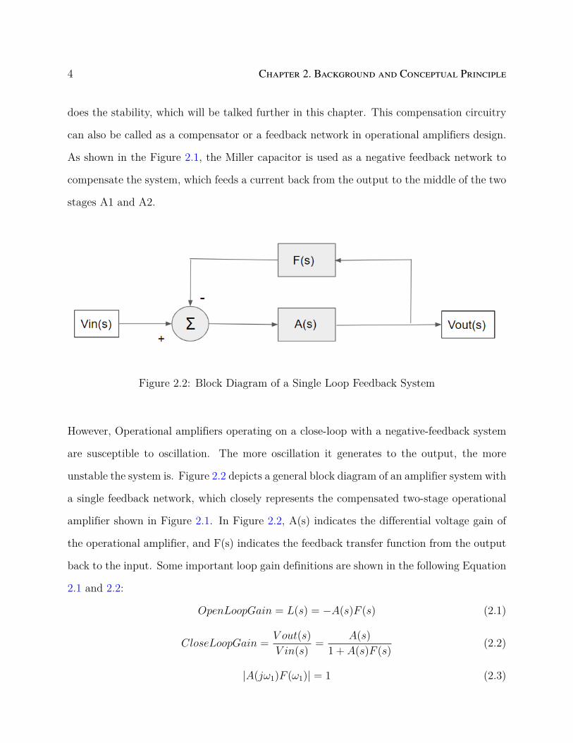
Figure 2.2: Block Diagram of a Single Loop Feedback System
However, Operational amplifiers operating on a close-loop with a negative-feedback system
are susceptible to oscillation. The more oscillation it generates to the output, the more
unstable the system is. Figure 2.2 depicts a general block diagram of an amplifier system with
a single feedback network, which closely represents the compensated two-stage operational
amplifier shown in Figure 2.1. In Figure 2.2, A(s) indicates the differential voltage gain of
the operational amplifier, and F(s) indicates the feedback transfer function from the output
back to the input. Some important loop gain definitions are shown in the following Equation
2.1 and 2.2:
OpenLoopGain = L(s) = −A(s)F (s) (2.1)
CloseLoopGain =V out(s)
V in(s)=
A(s)
1 + A(s)F (s)(2.2)
|A(jω1)F (ω1)| = 1 (2.3)
Page 17
2.1. BACKGROUND OF AMPLIFIER SYSTEM STABILITY 5
∠|A(ω1)F (ω1)| = −180◦ (2.4)
According to the Barkhausen’s Criterion, the oscillation condition of such system needs to
meet two requirements which are represented in Equation 2.3 and 2.4, where F(s) here is
considered as a constant [29]. The total phase shift of the system is 360◦ at ω1 because the
negative feedback network introduces a 180◦ phase shift. In this case, the circuit can amplify
its own noise until it eventually begins to oscillate at frequency ω1 [29].
Figure 2.3: Phase Margin Demonstration [8]
PhaseMargin = ϕM = Arg[−A(jω0dB)F (jω0dB)] = Arg[L(jω0dB)] (2.5)
One major criterion to measure the stability of this system is the phase margin, which is the
phase angle difference from the 0dB frequency to ±180◦ as shown in Equation 2.5 [7]. Phase
margin indicates system relative stability, and the tendency of oscillation during its response
to an input change such as a step function. Consider a step response of the second-order
system which models the closed-loop gain of the two-stage operational amplifier. Shown on
Figure 2.3, smaller phase margin tends to have larger overshoot and longer settling time to a
Page 18
6 CHAPTER 2. BACKGROUND AND CONCEPTUAL PRINCIPLE
step response input while larger phase margin can settle the output down quicker and has less
output oscillation. For most of the two-stage Op-Amp, designers want to settle the output
down quickly instead of letting it oscillate, so a large phase margin of a system is preferred,
which should be at least 45◦ and preferable 60◦ or larger. Also, too much overshoot has a
risk of damaging the output device.
Figure 2.4: Uncompensated Frequency Response of Two Stage Operational Amplifier [8]
Shown in Figure 2.4, the phase margin at ω0dB is close to 0◦ due to the two poles, which is
generated by the two stage amplifier, are below the unity gain frequency. Even though p2
is close to the unity gain frequency, it nearly drops another 90◦ to the phase margin. Due
to this major issue, the amplifier must have a compensation network to enlarge its phase
margin to at least 45◦ to ensure the stability of the whole system. One of the most common
approaches to address this issue is called Miller Compensation.
Page 19
2.2. COMPENSATED OP-AMP SURVEY 7
2.2 Compensated Op-Amp Survey
Before talking about the Miller compensation and all other techniques, a summarized survey
is listed below which includes and compares all the related topologies of compensations. This
survey compares some typical compensation designs including Miller Compensation, Miller
compensation with Nulling resistor, and Current buffer.
Referredpaper work
Millercompensation[25]
Miller compensationwith Nullingresistor[35]
Currentbuffer[28]
Supply Voltage(V) 2.9 - 3.7 5 3.3DC Gain(dB) 98.98 77.25 78.21
Gain Bandwidth(MHz) 2.22 14.1 5.82Phase Margin(◦) 81.5 85.85 63.97Slew Rate(V/µs) 1.37 9.4 5.58
Power Consumption (µW) - - 144.34CMRR(dB) 104.22 81 89.05PSRR(dB) 92.46 - 117.73
Table 2.1: Survey of various op amps topologies
Common mode rejection ratio (CMRR) is measured by: differential gain – common mode
gain, where differential gain is the DC gain [29], [25]. By applying this equation to all
three works, we can know the typical common mode gain range is around 4dB to 10dB.
Power supply rejection ratio (PSRR) measures the power supply noise rejection ability of
the amplifier, which are pretty high for all three designs ( over 80dB ). Due to the similarity
and stability of CMRR and PSRR of two-stage operational amplifier, this two parameters
will not be considered in the design and simulation in Chapter 3.
Page 20
8 CHAPTER 2. BACKGROUND AND CONCEPTUAL PRINCIPLE
2.3 Miller Compensation Technique Principle
Miller compensation is one of the most popular techniques that is used to increase the stabil-
ity of the Multi-stage amplifier. The design that is shown in Figure 2.5 is the configuration
of Miller compensation. The first stage of this Op-Amp consists of NMOS differential inputs
with a PMOS current mirror load, whereas the second stage is a PMOS common source
amplifier with a NMOS current mirror load. The compensation capacitor is connected be-
tween the output of these two stages, so this Compensation Capacitor CC is also called a
Miller Capacitor [12] [33] [32]. This typology can also be referred as a single capacitor Miller
compensation (SCMC) in some paper works [9]. Due to the direct connection of output and
input of the second stage, SCMC can also be called as Direct Feedback Compensation [34].
The working principle of Miller compensation is to split the poles so a higher phase margin
can be reached at the unity gain frequency [34]. However, a right-hand-plane (RHP) zero was
generated due to a feed forward current from the output of the first stage to the output of
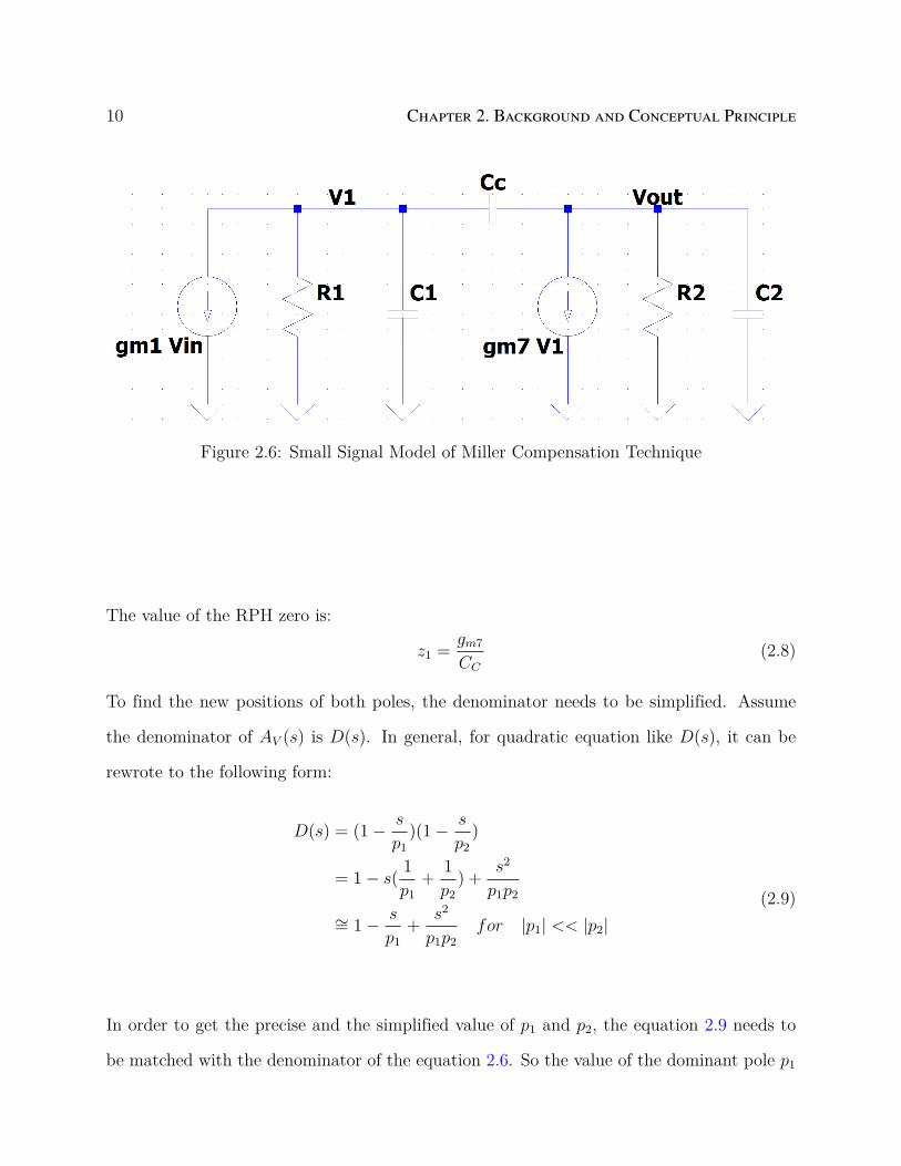
the second stage [10]. Before compensating the circuit, the two stage operational amplifier
has two poles which are located at p1 = 1R1C1
, and p2 = 1R2C2
, where R and C are the
resistance and capacitance respectively at the corresponding nodes shown in the Figure 2.6.
The capacitors C1 and C2 are mainly formed by the parasitic capacitance of corresponding
connected MOSFETs of each node. After the implementation of the Miller Capacitor, the
dominant pole and non-dominant pole are achieved due to the pole splitting. By using nodal
analysis at both input (V1) and output (V2) nodes of the common source stage, the system
gain equation can be generated as shown in equation 2.6, where the new positions of poles
Page 21
2.3. MILLER COMPENSATION TECHNIQUE PRINCIPLE 9
Figure 2.5: Two-Stage Op-Amp with Miller Compensation
and zero can also be found.
AV (s) =V out(s)
V in(s)=
gm1gm7R1R2(1− sCc
gm7)
1 + sa+ s2b
a = (C2 + CC)R2 + (C1 + CC)R1 + gm7R1R2CC ,
b = R1R2(C1C2 + C1CC + C2CC)
(2.6)
In equation 2.6, the DC gain and the position of zero can be noticed directly. The amplifier
DC gain is:
DC gain = gm1gm7R1R2 (2.7)
Page 22
10 CHAPTER 2. BACKGROUND AND CONCEPTUAL PRINCIPLE
Figure 2.6: Small Signal Model of Miller Compensation Technique
The value of the RPH zero is:
z1 =gm7
CC
(2.8)
To find the new positions of both poles, the denominator needs to be simplified. Assume
the denominator of AV (s) is D(s). In general, for quadratic equation like D(s), it can be
rewrote to the following form:
D(s) = (1− s
p1)(1− s
p2)
= 1− s(1
p1+
1
p2) +
s2
p1p2
∼= 1− s
p1+
s2
p1p2for |p1| << |p2|
(2.9)
In order to get the precise and the simplified value of p1 and p2, the equation 2.9 needs to
be matched with the denominator of the equation 2.6. So the value of the dominant pole p1
Page 23
2.3. MILLER COMPENSATION TECHNIQUE PRINCIPLE 11
is:
p1 =−1
(C2 + CC)R2 + (C1 + CC)R1 + gm7R1R2CC
∼=−1
gm7R1R2CC
(2.10)
The value of the non-dominant p2 is:
p2 = −(C2 + CC)R2 + (C1 + CC)R1 + gm7R1R2CC
R1R2(C1C2 + C1CC + C2CC)
∼= − gm7CC
C1C2 + C1CC + C2CC
∼= − gm7
C2 + C1
or, −gm7
C2
for C2 > CC > C1
(2.11)
As shown in Figure 2.7, the original open-loop poles p′1, and p′2 are split to the new position
Figure 2.7: Pole Splitting Demonstration [2]
p1 and p2 due to the Miller Compensation, where their values are shown in Equation 2.10
and 2.11. p1 becomes more dominant than it used to be, which results in the system starting
to behave as a first order system in low frequency range. On the contrary, p2 moves to
the other direction which makes it more non-dominant. The goal of splitting both poles is
achieved, however, a RHP zero z1 is generated, which is undesirable because it boosts the
Page 24
12 CHAPTER 2. BACKGROUND AND CONCEPTUAL PRINCIPLE
gain while decreasing the phase [22] [34]. One approach to address this issue is to make sure
its frequency is 10 times larger than the unity gain bandwidth frequency by adjusting the
corresponding parameter of z1 which is shown in Equation 2.8. This is the main reason that
the size of the compensation capacitor cannot be too large. To ensure at least 45◦ phase
margin, the effective frequency of the second pole p2 must be the same or larger than the
unity gain bandwidth as illustrated in the Figure 2.8. To obtain a higher phase margin, p2
needs to be moved to the left further in Figure 2.7 which is the high-frequency direction in
Figure 2.8, so that p2 has less effect of reducing the phase margin.
Figure 2.8: Compensated Frequency Response of Two Stage Operational Amplifier [2]
So the key point for now is to find the unity gain bandwidth shown as ‘GB’ in Figure 2.8,
which is the value of 0dB frequency. In this graph, the location of ‘GB’ is only affected by
the value of the dominant pole p1, where the gain starts to drop as a slope of -20dB/decade.
Page 25
2.3. MILLER COMPENSATION TECHNIQUE PRINCIPLE 13
So the relationship of these variables can be derived as the equation below:
20log10(AV (0)) = [log10(GB)− log10(|p1|)]× 20
log10(AV (0)) = log10(GB
|p1|)
GB = AV (0)× |p1|
GB =gm1gm7R1R2
gm7R1R2CC
GB =gm1
CC
(2.12)
Suppose the required phase margin for stability is 60◦, then the location of p2 can be esti-
mated from this phase requirement by using the following equation:
180◦ − tan−1 ω
|p1|− tan−1 ω
|p2|− tan−1 ω
|z1|= PM = 60◦ (2.13)
Let ω be equal to the unity gain bandwidth frequency GB in the previous equation and
assume z1 is 10 times larger than GB, then the following equation can be obtained [2]. The
main reason to let z1 10 times larger than GB is to shrink its effect of phase margin.
180◦ − tan−1GB
|p1|− tan−1GB
|p2|− tan−1GB
|z1|= PM = 60◦
180◦ − tan−1AV (0)− tan−1GB
|p2|− tan−1(0.1) = 60◦
180◦ − 90◦ − 60◦ − 5.7 = tan−1GB
|p2|
tan−1GB
|p2|= 24.3◦ → GB
|p2|= 0.452
|p2| > 2.215×GB
(2.14)
Then the relationship of the trans-conductance gm of Mosfets can be obtained by applying
the Equation 2.8, 2.11, and 2.12 to the assumption above. The relationship between gm7
Page 26
14 CHAPTER 2. BACKGROUND AND CONCEPTUAL PRINCIPLE
and gm1 is restricted by the assumption that z1 is 10 times larger than GB, which is shown
in the following equation.
z1 ≥ 10×GB
gm7
CC
≥ 10× gm1
CC
gm7 ≥ 10gm1
(2.15)
The value of the compensation capacitor CC can be estimated through the relationship
between p2 and GB that is shown in Equation 2.16. Knowing that C2 is the capacitance
corresponding to the output node which parasitic capacitances are relatively small compared
with the load capacitor CL, so we can assume C2 is equal to the load capacitor for easy
calculations.
|p2| ≥ 2.215×GB
gm7
C2
≥ 2.215× gm1
CC
10gm1
C2
≥ 2.215× gm1
CC
CC ≥ 0.2215CL
(2.16)
Overall, to obtain a phase margin at least 60◦ for stability, CC needs to be the same or larger
than the 0.2215 times C2. Also, gm7 needs to be at least 10 times of gm1. The positions of
both poles and zero should be at the correct locations with respect to unity gain frequency.
However, there are still several trade-offs in real world design of Two Stage Amplifiers. For
example, increasing gm7 can separate the poles more but costs more power. Making the CC
too large may not help with the phase margin as ωz1 will reduce too. Large CC could also
Page 27
2.4. NULLING RESISTOR TECHNIQUE PRINCIPLE 15
reduce the unity gain bandwidth. So to obtain a better stability of two-stage Op-Amps, the
RHP zero must be addressed. There are several ways to get rid of this RHP zero, and one
of the most common approaches is adding Nulling Resistor which could move this zero from
the right plane to the left [22].
2.4 Nulling Resistor Technique Principle
2.4.1 Nulling Resistor Technique Background
As talked in the last section, adding a nulling resistor in series with the compensation
capacitor is one of the most common approaches to eliminate the negative effect of the RHP
zero by moving this zero to the LHP [21] [17] [14] [11]. Figure 2.10 depicts the pole splitting
phenomenon and shows all the locations of poles and zero. This nulling resistor RZ can
either be an actual resistor or a transistor as shown in Figure 2.9. The transistor used in
(a) Nulling Resistor with Actual Resistor (b) Nulling Resistor with Transistor
Figure 2.9: Compensated Two-Stage Op-Amp with Nulling Resistor
Figure 2.9b is PMOS, which can also be replaced by a NMOS transistor by connecting its
Page 28
16 CHAPTER 2. BACKGROUND AND CONCEPTUAL PRINCIPLE
Figure 2.10: Locations of Ploes and the Zero [22]
gate terminal to V dd. Instead of using a single transistor here, a CMOS switch can be used
to avoid dynamic range limitation in some specific applications [18]. This CMOS technology
switch is also known as a Transmission Gate that connects a NMOS and a PMOS transistor
in parallel as illustrated in Figure 2.11.
Figure 2.11: Transmission Gate [18]
For this configuration, when Q is low, both transistors are off, and the transmission gate is
off. When Q is high, both transistors are on, creating a low resistance close loop circuit. So
in this case, the signal Q is connected to a high voltage node which is usually the V dd while
the signal Q is connected to a low voltage node which is always the ground. The resistance
values of the both PMOS and NMOS are obtained from Equation 2.17 and 2.18, which are
derived in [29].
Page 29
2.4. NULLING RESISTOR TECHNIQUE PRINCIPLE 17
RON =1
µnCoxWL(VGS − VTHn)
(2.17)
ROP =1
µpCoxWL(VSG − VTHp)
(2.18)
For the PMOS and the NMOS transistors in this transmission gate, their overdrive voltages
are much bigger than the absolute value of their drain to source voltages (|Vds|). So both
transistors work in deep triode regions which operate like voltage controlled resistors [29].
In this situation, the overdrive voltage is nearly stable so the resistance value can only be
changed by adjusting the parameter WL
based on the Equation 2.17 and 2.18. Both equations
also work for a single MOSFET that is used as a nulling resistor in the compensation network.
2.4.2 Nulling Resistor Technique Frequency Response
Similar to the Miller Compensation Technique, to know the effect of the adding resistor, we
need to find all the poles and zeros through the small signal analysis. By applying nodal
Figure 2.12: Small Signal Model of Nulling Resistor Technique
analysis to both V1 and Vout nodes in Figure 2.12, the relationship of output and input signals
can be derived, where we can find all the poles and zeros. The derivation is nearly the same
Page 30
18 CHAPTER 2. BACKGROUND AND CONCEPTUAL PRINCIPLE
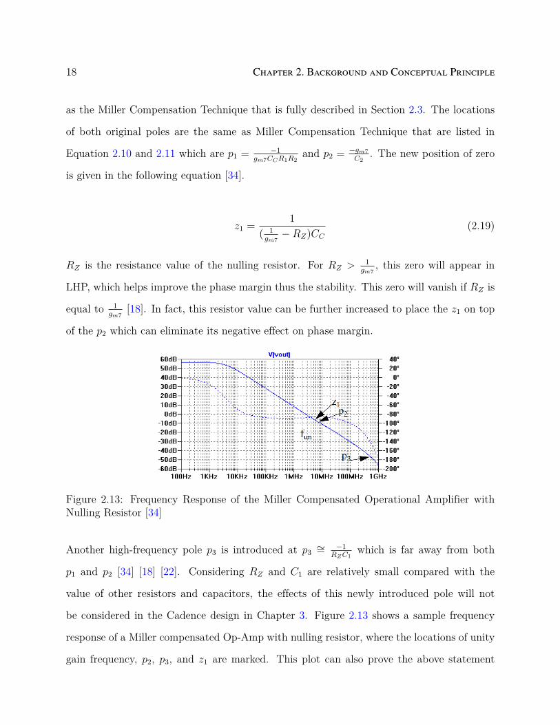
as the Miller Compensation Technique that is fully described in Section 2.3. The locations
of both original poles are the same as Miller Compensation Technique that are listed in
Equation 2.10 and 2.11 which are p1 =−1
gm7CCR1R2and p2 =
−gm7
C2. The new position of zero
is given in the following equation [34].
z1 =1
( 1gm7
−RZ)CC
(2.19)
RZ is the resistance value of the nulling resistor. For RZ > 1gm7
, this zero will appear in
LHP, which helps improve the phase margin thus the stability. This zero will vanish if RZ is
equal to 1gm7
[18]. In fact, this resistor value can be further increased to place the z1 on top
of the p2 which can eliminate its negative effect on phase margin.
Figure 2.13: Frequency Response of the Miller Compensated Operational Amplifier withNulling Resistor [34]
Another high-frequency pole p3 is introduced at p3 ∼= −1RZC1
which is far away from both
p1 and p2 [34] [18] [22]. Considering RZ and C1 are relatively small compared with the
value of other resistors and capacitors, the effects of this newly introduced pole will not
be considered in the Cadence design in Chapter 3. Figure 2.13 shows a sample frequency
response of a Miller compensated Op-Amp with nulling resistor, where the locations of unity
gain frequency, p2, p3, and z1 are marked. This plot can also prove the above statement
Page 31
2.5. VOLTAGE BUFFER TECHNIQUE PRINCIPLE 19
regarding p3, as the value of p3 is over 100 times away from the unity gain frequency.
2.5 Voltage Buffer Technique Principle
Instead of changing the location of the RHP zero, a voltage buffer can be used to eliminate
this zero by rejecting the feed-forward path through the Miller Capacitor in the feedback path
[24] [16]. At the same time, the feedback network should work functionally. So a common
gate amplifier can be used here as the voltage buffer which blocks the feed-forward current
and allows the feedback current that flows from the output to the input of the second stage.
Figure 2.14 is a block diagram of this methodology and Figure 2.15 is a sample schematic
that is implemented by NMOS and PMOS transistors respectively.
Figure 2.14: Block Diagram of Voltage Buffer Implementation [2]
One drawback of this method is one more path costs additional power and transistors. Also,
there is a fixed voltage drop in the feedback network due to the use of the voltage follower
[34]. This voltage could reduce the output voltage swing [34]. The maximum and the
minimum V out of both cases is V dd and ground, which means the source follower might
work as a diode connected MOSFET but never in the triode region. So the feedback signal
will never get broken down by large V out which is a opposite in [34]. One advantage is
that this topology makes frequency response simple since the zero is removed and both poles
Page 32
20 CHAPTER 2. BACKGROUND AND CONCEPTUAL PRINCIPLE
Figure 2.15: Compensated Two-Stage Op-Amp with Voltage Buffer [34]
remain at the same locations which are p1 =−1
gm7CCR1R2and p2 =
−gm7
C2. Also, all the negative
effects of this RHP zero disappear.
2.6 Indirect Compensation Technique Principle
2.6.1 Indirect Compensation Background
Miller compensation is achieved by connecting the feedback network directly from the output
to the input of the second stage. This feedback network can also be fed back indirectly
from the output to an internal high impedance node, which is called Indirect Feedback
Compensation [34] [5]. The feedback path is connected to an internal low impedance node
in the first stage, which allows indirect feedback of the compensation current from the output
node to the internal high-impedance node which is the output of the first stage [31] [13].
Shown in Figure 2.16 is the block diagram of an indirect compensation 2-stage Op-Amp,
where the low impedance node is marked as Zlow. Indirect compensation can be achieved by
several approaches as long as a low impedance node can be found in the first stage, such as
Page 33
2.6. INDIRECT COMPENSATION TECHNIQUE PRINCIPLE 21
adding a common gate stage, cascoded current mirror load, and cascoded differential inputs
pair[31] [34].
Figure 2.16: Block Diagram of Indirect Compensation [8]
2.6.2 Common Gate Stage (Current Buffer) Compensation
Figure 2.17: 2 Stage Op-Amp with Common Gate Stage Compensation [34]
Page 34
22 CHAPTER 2. BACKGROUND AND CONCEPTUAL PRINCIPLE
As shown in Figure 2.17, the current sources M9, M10 and the common gate amplifier MCG
configures the indirect compensation stage. This idea is first introduced by Ahuja in his
paper which was published in 1983 [1]. So this common gate compensation is also called
Ahuja compensation. Since this stage does not share components with the original 2 stages
of the Op-Amp, this stage can be referred to as a ”separate, additional” stage [10]. This
common gate stage can also block the feed-forward current path and allow the feedback
current as the common drain stage [10] [34] [27]. So based on this statement, if the common
gate stage is modeled as an ideal current buffer, the RHP zero could be eliminated [10].
However, in the following analysis, the current buffer is not assumed to be ideal. In order
to obtain and analyze the relationship of the output and the input, the small signal model
of this common gate stage Op-Amp is derived and shown in Figure 2.18, where RA and
CA are the resistance and capacitance at the low impedance node A. V s is denoted as the
differential pair inputs which is equal to Vp - Vm.
Figure 2.18: Small Signal Model of Common Gate Stage Compensation Op-Amp [34] [13][10]
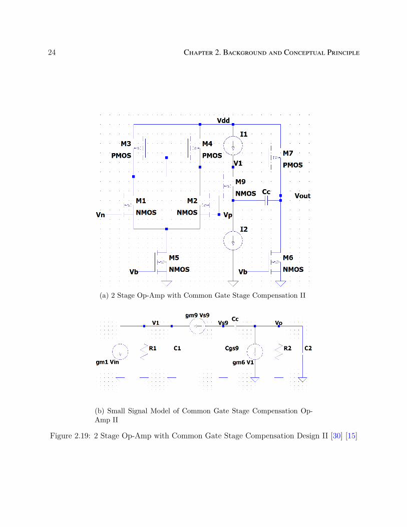
In all [34] [13], and [10], they all used the same small signal model in Figure 2.18, and all
these papers were published before 2010. However, the equivalent small signal model is
presented differently in a recent published paper [30]. The same design idea is also depicted
in [15]. Shown in Figure 2.19a, the basic working idea is the same where the current source
Page 35
2.6. INDIRECT COMPENSATION TECHNIQUE PRINCIPLE 23
MOSFETs are represented by the ideal current sources I1, and I2. But the small signal
model is partially different regarding the common gate stage, which is in between of the
2-stage Op-Amp. More specifically, the overdrive voltage controlled current source (gm9Vgs9)
is placed between the source node (Vs9) and the drain node (V 1) as shown in Figure 2.19b.
However, in Figure 2.18 this dependent current source is connected from the V s9 to ground.
The second design is preferred in my opinion even though it does not consider the resistance
of ideal current sources. However, all the estimated poles and zero locations are the same
no matter what small signal models are used.
According to the small signal model in Figure 2.18, there are three voltage nodes and hence
three dependent variables, V 1, VA, and V 2 or V out. So by applying the nodal analysis on
each node, three equations of all these variables can be derived.
− gm1Vs +V1
R1
+ V1sC1 − gmcVA +V1 − VA
rOC= 0 (2.20)
gm2V1 +Vout
R2
+ VoutsC2 + sCC(Vout − VA) = 0 (2.21)
VA − V1
rOC
+ gmcVA +VA
RA
+ VAsCA + sCC(VA − Vout) = 0 (2.22)
The transfer function of the amplifier system can be obtained from these equations and its
simplified from is shown in the following equation, where assumptions C2∼= CL; and CC , C2
Page 36
24 CHAPTER 2. BACKGROUND AND CONCEPTUAL PRINCIPLE
(a) 2 Stage Op-Amp with Common Gate Stage Compensation II
(b) Small Signal Model of Common Gate Stage Compensation Op-Amp II
Figure 2.19: 2 Stage Op-Amp with Common Gate Stage Compensation Design II [30] [15]
Page 37
2.6. INDIRECT COMPENSATION TECHNIQUE PRINCIPLE 25
» C1, CA are applied [34].
Vout
Vs
= AV (b0 + b1s
a0 + a1s+ a2s2 + a3s3)
AV = gm1gm2R1R2
b0 = gmcRArOC
b1 = RArOC(CC + CA)
a0 = (gmcRA + 1)rOC
a1 = (gmcRA + 1)gm2R1R2rOCCC
a2 = (gmcRA + 1)R1R2rOCC1(C2 + CC) +R2RAC2[rOC(CC + CA) +R1(CC + CA + C1)]
a3 = R1R2RAC1rOC(C2CA + C2CC + CCCA)
(2.23)
The location of the zero can be obtained from the numerator of this transfer function which
is at:
z1 = −b0b1
= − gmc
CC + CA
(2.24)
Obviously, this zero is located on the LHP and the key point here is this zero is on the LHP
instead of RHP for a finite value of gmc [10].
The amplifier has three poles from the denominator of the transfer function where the loca-
tion of the dominant pole p1 is derived in Equation 2.25 if the assumption |p1| » |p2|, |p3| is
applied [10] [34] [13].
p1 = −a0a1
= − 1
gm2R2R1CC
(2.25)
Page 38
26 CHAPTER 2. BACKGROUND AND CONCEPTUAL PRINCIPLE
By comparing this location with the p1 from Miller Compensation in Equation 2.10, the
dominant pole does not move. Based on the assumption that the other poles are far away
from p1, so for s » p1, the denominator of the transfer function could be rewritten as:
D(s) ∼= (1− s
p1)(1 +
a2a1
s+a3a1
s2) (2.26)
The second part of the denominator can be rewritten as a form showing the locations of p2
and p3, which is denoted as D′(s).
D′(s) = (1− s
p2)(1− s
p3)
= 1− s(1
p2+
1
p3) +
s2
p3p2
∼= 1− s
p2+
s2
p3p2for |p2| << |p3|
(2.27)
From the above equation, locations of the non-dominant poles p2, and p3 can be obtained.
p2 = −a1a2
= − gm2CC
C1(CC + C2)∼=
gm2CC
C1CL
(2.28)
p3 = −a2a3
∼= −(gmc
C2||CC
+1
C1(R1||ROC)) ∼= − gmc
C2||CC
(2.29)
Comparing the second pole form the Miller Compensation in Equation 2.11. The second
pole value is enlarged from gm2
CLto gm2CC
C1CLby a factor of CC
C1. Also, to let the third pole p3 be
Page 39
2.6. INDIRECT COMPENSATION TECHNIQUE PRINCIPLE 27
far away from the second pole, the gmc should be large as the equation shown below.
|p3| >> |p2|gmc
C2||CC
>>gm2CC
C1(CC + C2)
gmc >>gm2CC(C2||CC)
C1(CC + C2)
(2.30)
So if gmc → ∞, then the third pole p3 → ∞ according to Equation 2.29 [1]. With the
positive effect of the LHP zero, the phase margin could be increased. Since p1 is the same
as the one in Miller Compensation, p2 is increased by a factor of CC
C1, and p3 is far away from
the unity gain bandwidth, the overall circuit design ideas and some performance trade-offs
are nearly the same as talked in Section 2.3. One more consideration is the added common
gate stage which includes gmc and other related parameters from current sources. This stage
gives more flexibility to choose their parameters values because this stage is additional and
separate [10]. However, one restriction of gmc that must be considered is shown in Equation
2.30. It signifies that the indirect path has to be much faster than the output stage which
thus relocates non-dominant poles to higher frequency and thus improving the unity gain
frequency [13].
Based on the further observation from Equation 2.24 and Equation 2.29, the non-dominant
pole p3 could be overlapped with the location of the only zero if the parasitic capacitance
CA « CC [13]. Then this Op-Amp works as a Miller Compensated Two-stage Op-Amp with
the Voltage Buffer which is talked in Section 2.5.
This common gate stage is proved to deliver wider unity gain bandwidth, higher PSRR and
faster response than the Miller compensation [30] [28]. It also overcomes one drawback of the
voltage buffer technique that reduces the output swing of the Op-Amp [28]. Some drawbacks
regarding this design are that extra transistors are needed to implement the common gate
Page 40
28 CHAPTER 2. BACKGROUND AND CONCEPTUAL PRINCIPLE
stage. Also, mismatch between the current sources changes the bias currents in the input
stage which affects the input-offset voltage of the op-amp [10].
Page 41
Chapter 3
Two Stage Operational Amplifier
Designs and Simulation Results
3.1 Design Specifications
The specifications that are shown in Table 3.1 will be used to design a two-stage operational
amplifier. This table will be used as a standard performance to evaluate different compen-
sation techniques including direct and indirect compensation feedback networks. All these
techniques are demonstrated in detail in Chapter 2.
Parameter ValueDC Gain 70 dB
Gain Bandwidth ≥ 25 MHzPhase Margin ≥ 60◦
Slew Rate ≥ 15V/µs (preferably ≥ 20V/µs)Power Consumption 0.3 nW
Table 3.1: Design Specifications of Two Stage Amplifier
29
Page 42
30 CHAPTER 3. TWO STAGE OPERATIONAL AMPLIFIER DESIGNS AND SIMULATION RESULTS
3.2 Cadence Design and Simulation Result of Tradi-
tional Miller Compensation
3.2.1 Design Procedure
Listed below are some useful equations regarding design parameters that will be considered
when designing the Miller compensation Op-Amp. Equations 3.2, 3.3, and 3.4 are derived
in Section 2.3 as Equations 2.12, 2.15 and 2.16 respectively.
gm =
√2µn,pCox
W
LId (3.1)
GB =gm1
CC
(3.2)
gm7 ≥ 10gm1 (3.3)
CC ≥ 0.2215C2 (3.4)
rO =1
Iλ(3.5)
First Stage Gain AV 1 = −gm1(rO1,2||rO3,4)
=−2gm1
I5(λ1,2 + λ2,4)
(3.6)
Second Stage Gain AV 2 = −gm7(rO7||rO6)
=−gm7
I6(λ7 + λ6)
(3.7)
Slew Rate =I5CC
(3.8)
Generally, as stated in the last chapter, the main goal to design an amplifier is to have a
high gain but also stable, which does not consume a lot of power but can also respond to
Page 43
3.2. CADENCE DESIGN AND SIMULATION RESULT OF TRADITIONAL MILLER COMPENSATION 31
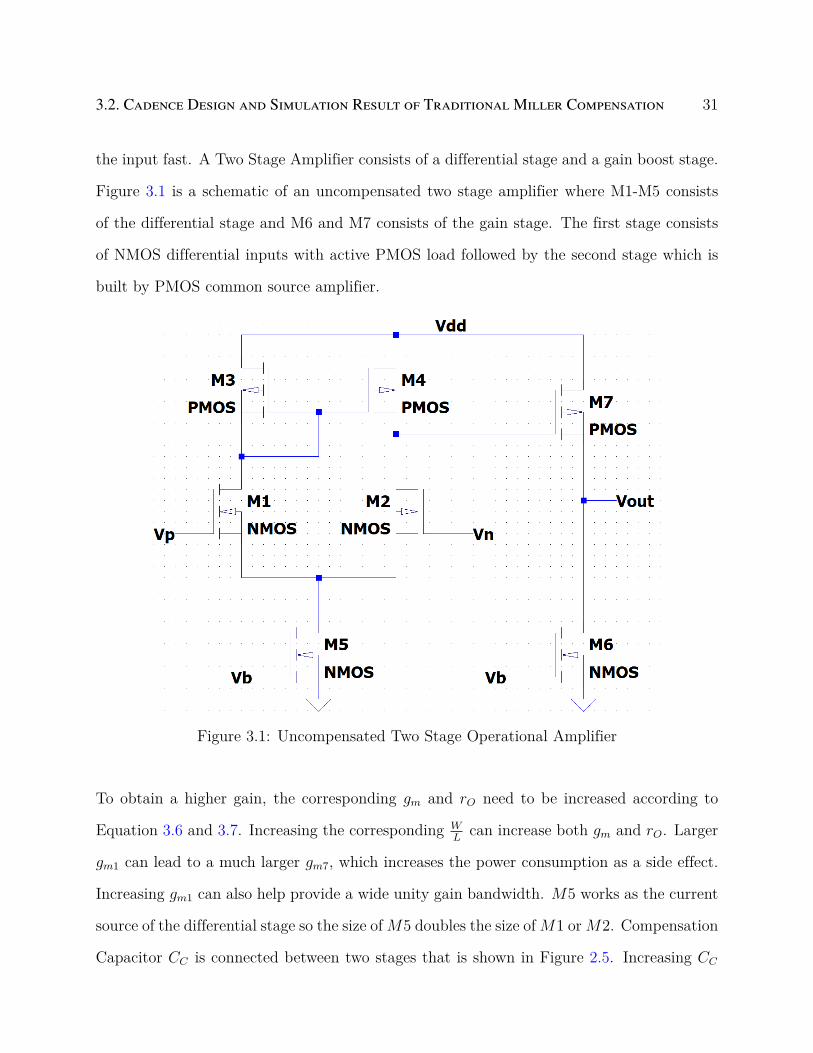
the input fast. A Two Stage Amplifier consists of a differential stage and a gain boost stage.
Figure 3.1 is a schematic of an uncompensated two stage amplifier where M1-M5 consists
of the differential stage and M6 and M7 consists of the gain stage. The first stage consists
of NMOS differential inputs with active PMOS load followed by the second stage which is
built by PMOS common source amplifier.
Figure 3.1: Uncompensated Two Stage Operational Amplifier
To obtain a higher gain, the corresponding gm and rO need to be increased according to
Equation 3.6 and 3.7. Increasing the corresponding WL
can increase both gm and rO. Larger
gm1 can lead to a much larger gm7, which increases the power consumption as a side effect.
Increasing gm1 can also help provide a wide unity gain bandwidth. M5 works as the current
source of the differential stage so the size of M5 doubles the size of M1 or M2. Compensation
Capacitor CC is connected between two stages that is shown in Figure 2.5. Increasing CC
Page 44
32 CHAPTER 3. TWO STAGE OPERATIONAL AMPLIFIER DESIGNS AND SIMULATION RESULTS
can stabilize the system more by enlarging the phase margin but can also shrink the unity
gain bandwidth and decrease the slew rate. Another factor that needs to be considered
is the voltage level including the gate voltage of the current source (Vb) and the common
mode voltage (VCM) of both inputs, which is also important to set all the MOSFETs in
saturation region. Overall, the main design parameters are WL
of all the MOSFETs and the
compensation capacitor CC , which will be adjusted in the process of Cadence design based
on the statements above to reach the standard performance.
3.2.2 Cadence Design Result
Considering all the relationships and restrictions among all the parameters, all the design
parameters are properly sized. The ratio of all the MOSFETs of the Miller compensated
amplifier is shown in Table 3.2. The actual values of all the parameters are presented in the
Cadence Schematic Design shown in Figure 3.2.
Transistor WL
ratioM1, M2 15M3, M4 20
M5 30M6 50M7 166.7
Table 3.2: Transistor Sizing
Figure 3.2 depicts the Miller Compensation Op-Amp where the compensation capacitor CC
is set to 500fF as the load capacitor is 1pF that is not shown in this figure. Also, both V b
and the common mode voltage of inputs are set to 500mV .
All the results are listed in Table 3.3 after running the simulation. The DC gain and the
positive edge slew rate meets the requirement, however, the phase margin trades off with
Page 45
3.2. CADENCE DESIGN AND SIMULATION RESULT OF TRADITIONAL MILLER COMPENSATION 33
Parameter ValueDC Gain 71.62 dB
Gain Bandwidth 22.43 MHzPhase Margin 57.8◦
Positive Edge Slew Rate (SR+) 29.11V/µsNegative Edge Slew Rate (SR−) 15.6V/µs
Power Consumption 150 µW
Table 3.3: Results of Miller Compensation Amplifier
the Gain Bandwidth. Wider unity Gain Bandwidth always shrinks the phase margin which
proves the statements in Section 2.3. Figure 3.3 shows the Bode Plot of gain and phase while
the Figure 3.4 shows the output response of a step function where the slew rate is measured.
Figure 3.5 depicts the Cadence Design test benches, where the load capacitor CL is attached.
Figure 3.2: Design Schematic of Miller Compensation Amplifier
Page 46
34 CHAPTER 3. TWO STAGE OPERATIONAL AMPLIFIER DESIGNS AND SIMULATION RESULTS
Figure 3.3: Frequency Response of Miller Compensation Amplifier
Page 47
3.2. CADENCE DESIGN AND SIMULATION RESULT OF TRADITIONAL MILLER COMPENSATION 35
Figure 3.4: Output Response of a Step Function Input
Figure 3.5: Test Bench of Miller Compensation Amplifier
Page 48
36 CHAPTER 3. TWO STAGE OPERATIONAL AMPLIFIER DESIGNS AND SIMULATION RESULTS
3.3 Cadence Design and Simulation Result of Nulling
Resistor Technique
3.3.1 Design Procedure
The whole design procedure is nearly the same as the previous section (traditional Miller
compensation) instead of finding the proper position of z1. Some useful equations that help
locate the correct position of z1 are listed below.
z1 =1
( 1gm7
−RZ)CC
(3.9)
RON =1
µnCoxWL(VGS − VTHn)
(3.10)
ROP =1
µpCoxWL(VSG − VTHp)
(3.11)
The MOS transistor is picked as RZ in the whole design, which resistance depends on its
overdrive voltage and WL
. Since the gate terminal is connected to either the V dd or ground,
the overdrive voltage is considered to be nearly stable. So the design parameters is WL
of
this transistor. To make sure the zero appears in the LHP, RZ needs to be larger than 1gm7
,
according to Equation 3.9. Further derivation is illustrated in the Equation 3.12.
RZ >1
gm7
1
µCoxWL(|VGS − VTH)|
>1
µpCoxWL(|VGS − VTH)|
1
µWLVod(RZ)
>1
µpWLVod(M7)
µ(W
L)RZVod(RZ) < µp(
W
L)RZVod(M7)
(3.12)
Page 49
3.3. CADENCE DESIGN AND SIMULATION RESULT OF NULLING RESISTOR TECHNIQUE 37
Based on this derivation, PMOS is preferred due to its smaller electron mobility µ compared
with NMOS, so the ratio of WL
is smaller for PMOS. This could help reduce the size of the
design area. The overdrive voltage is depending on lots of parameters that is impossible to
be precisely determined in this situation. In Equation 3.9, CC is another factor that can
change the position of this zero. Under this condition, CC could be decreased to increase the
unity gain bandwidth according to Equation 3.2. At the same time, the ratio of WL
must be
reduced so the zero can be kept at around the same spot. The advantage of this adjustment
is increasing the phase margin and the unity gain bandwidth at the same time. So the main
design parameter of the nulling resistor is the ratio WL
of this added PMOS transistor.
3.3.2 Cadence Design Result
Knowing from Section 3.2.2, using one single Miller Capacitor in the feedback network is
hard to meet all the required standards. However, adding a nulling resistor in series with the
capacitor can improve the performance of the amplifier in stability and unity gain bandwidth.
To reach all the requirements from Table 3.1, all the design parameters are properly adjusted
and sized. The ratio of WL
of each transistor is shown in Table 3.4.
Transistor WL
ratioM1, M2 15M3, M4 20
M5 30M6 50M7 166.7M8 5.6
Table 3.4: Transistor Sizing
Figure 3.6 shows the Cadence design schematic of the Op-Amp where all the parameters
are labeled. All transistors keep the same size but the size of the compensation capacitor is
Page 50
38 CHAPTER 3. TWO STAGE OPERATIONAL AMPLIFIER DESIGNS AND SIMULATION RESULTS
reduced to 400fF . The output capacitor is still 1pF that is now shown in this graph. V dd
and V b keep the same, which are 1.8V and 500mV respectively.
Figure 3.6: Design Schematic of Amplifier with Nulling Resistor
Parameter ValueDC Gain 71.62 dB
Gain Bandwidth 27.1 MHzPhase Margin 65.4◦
Positive Edge Slew Rate (SR+) 36.36V/µsNegative Edge Slew Rate (SR−) 16.55V/µs
Power Consumption 149.8 µW
Table 3.5: Results of 2 Stage Amplifier with Nulling Resistor
All the results, that are listed in Table 3.5, meet all the requirements. Figure 3.7 shows the
Page 51
3.3. CADENCE DESIGN AND SIMULATION RESULT OF NULLING RESISTOR TECHNIQUE 39
Bode Plot of gain and phase while the Figure 3.8 shows the output response of a step function
where the slew rate is measured. Figure 3.9 depicts the Cadence design test benches where
the load capacitor is added. Slew rate is increased compared with the Miller compensation
result because the value of CC is smaller. So overall, by comparing Table 3.5 with Table 3.3,
adding a nulling resistor in series with the compensation capacitor improves the performance
of the amplifier in phase margin, the unity gain bandwidth, and the positive edge slew rate.
Figure 3.7: Frequency Response of Amplifier with Nulling Resistor
Page 52
40 CHAPTER 3. TWO STAGE OPERATIONAL AMPLIFIER DESIGNS AND SIMULATION RESULTS
Figure 3.8: Output Response of a Step Function Input
Figure 3.9: Test Bench of Miller Compensation Amplifier with Nulling Resistor
Page 53
3.4. CADENCE DESIGN AND SIMULATION RESULT OF VOLTAGE BUFFER TECHNIQUE 41
3.4 Cadence Design and Simulation Result of Voltage
Buffer Technique
The implementation of the voltage buffer onto the Op-Amp is fully illustrated in Section
2.5. This voltage buffer can be achieved by either using a PMOS source follower or a NMOS
source follower. NMOS source follower is picked in this design since the existing drive voltage
of NMOS current source. Shown in the Figure 3.10, NMOS M9 and M8 have the same size
which work as a current source and a source follower respectively. The size of all other
transistors and the compensation capacitor is also presented in this schematic, which is the
same as nulling resistor technique.
Figure 3.10: Design Schematic of Amplifier with Voltage Buffer
The ratio WL
of each transistor is shown in Table 3.6. The compensation capacitor is set to
Page 54
42 CHAPTER 3. TWO STAGE OPERATIONAL AMPLIFIER DESIGNS AND SIMULATION RESULTS
be 400fF , while the output capacitor is set to be 1pF that is not presented in the schematic.
V dd and V b keep the same, which are 1.8V and 500mV respectively.
Transistor WL
ratioM1, M2 15M3, M4 20
M5 30M6 50M7 166.7M8 11.1M9 11.1
Table 3.6: Transistor Sizing
All the results are listed in Table 3.7. The improvement of phase margin, unity gain band-
width, and slew rate are dramatic. This result can also reflect how negatively the RHP
zero affects. By removing this zero, this Op-Amp becomes more stable, has a wider range
of application frequency, and is able to respond faster. The only drawback is more power
consumption due to source follower path. All in all, the Op-amp with the source follower in
the feedback network scores the best results so far.
Parameter ValueDC Gain 71.62 dB
Gain Bandwidth 34.67 MHzPhase Margin 74.19◦
Positive Edge Slew Rate (SR+) 57.88V/µsNegative Edge Slew Rate (SR−) 23.72V/µs
Power Consumption 180 µW
Table 3.7: Results of 2 Stage Amplifier with Voltage Buffer
Figure 3.11 shows the Bode Plot of gain and phase while Figure 3.12 shows the output
response of a step function where the slew rate is measured. Test benches and the load
Page 55
3.4. CADENCE DESIGN AND SIMULATION RESULT OF VOLTAGE BUFFER TECHNIQUE 43
capacitor keep the same as the previous section.
Figure 3.11: Frequency Response of Amplifier with Voltage Buffer
Page 56
44 CHAPTER 3. TWO STAGE OPERATIONAL AMPLIFIER DESIGNS AND SIMULATION RESULTS
Figure 3.12: Output Response of a Step Function Input
Page 57
3.5. CADENCE DESIGN AND SIMULATION RESULT OF COMMON GATE COMPENSATION 45
3.5 Cadence Design and Simulation Result of Common
Gate Compensation
The whole design idea of the common gate compensation is very similar to Miller Compen-
sation instead of additional adjustments regarding the common gate compensation. Some
useful equations are listed below which are derived in Section 2.6.2.
p1 = − 1
gm2R2R1CC
(3.13)
p2 = − gm2CC
C1(CC + C2)∼=
gm2CC
C1CL
(3.14)
p3 = −(gmc
C2||CC
+1
C1(R1||ROC)) ∼= − gmc
C2||CC
(3.15)
z1 = −b0b1
= − gmc
CC + CA
(3.16)
gmc >>gm2CC(C2||CC)
C1(CC + C2)(3.17)
From Equation 3.15, 3.16, and some theories that are talked in Section 2.6.2, gmc needs to
be large so that p3 and z1 can be pushed away from the unity gain bandwidth so do their
effects on phase margin. According to Equation 3.1, a large value of gmc can be given by a
large ratio of corresponding WL
combined with large related current. So the corresponding
two current sources (M8, M9) of this stage need to be adjusted to support this condition.
During the design process, the value of the compensation capacitor CC is also increased due
to the position of p2 and its negative effect on phase margin. So CC is increased to 800fF to
push p2 away from the unity gain bandwidth. After increasing the value of the compensation
capacitor, gmc needs an equivalent increment based on Equation 3.17. The current loads M3
and M4, and the current mirror load M6 are also adjusted to maintain the sufficient gain.
Page 58
46 CHAPTER 3. TWO STAGE OPERATIONAL AMPLIFIER DESIGNS AND SIMULATION RESULTS
The entire schematic of common gate compensation two-stage Op-Amp is shown in Figure
3.13, where all the values of parameters are labeled.
Figure 3.13: Design Schematic of Amplifier with Common Gate Compensation
Transistor WL
ratioM1, M2 15M3, M4 30
M5 30M6 83.3M7 166.7
MCG 18.75M8 18.75M9 37.5
Table 3.8: Transistor Sizing
The ratio WL
of each transistor is shown in Table 3.8. The compensation capacitor is set to
be 800fF , while the output capacitor is set to be 1pF that is not presented in the schematic.
Page 59
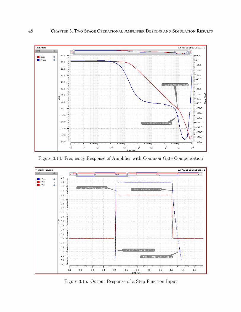
3.5. CADENCE DESIGN AND SIMULATION RESULT OF COMMON GATE COMPENSATION 47
V dd and V b keep the same, which are 1.8V and 500mV respectively. Figure 3.14 depicts
the Bold Plot, and Figure 3.15 shows the output response of a step input function, where
the slew rate is measured.
Parameter ValueDC Gain 70.83 dB
Gain Bandwidth 85.4 MHzPhase Margin 62.56◦
Positive Edge Slew Rate (SR+) 366.9V/µsNegative Edge Slew Rate (SR−) 21.74V/µs
Power Consumption 261u W
Table 3.9: Results of 2 Stage Amplifier with Voltage Buffer
Both DC gain and phase margin meets the standard requirements but the cost is increasing
the size of CC . The improvement of unity gain bandwidth is remarkable compared with
Miller Compensation. The major reason of the unity gain bandwidth increment is because
the dominant pole p1 is pushed to the higher frequency direction by observing the frequency
response of Miller Compensation and common gate compensation (Figure 3.3, and 3.14).
This is mainly caused by increased CC according to Equation 3.13. The non-dominant poles
p2 and p3 with the zero z1 are located at higher frequency regarding to unity gain frequency,
however, they still have little effect on phase margin of the Op-Amp system by looking at the
phase plot (Figure 3.14) at the unity gain frequency. The positive edge slew rate has a huge
difference with the negative edge slew rate which is also caused by the increased value of
the compensation capacitor CC . Power Consumption is also increased due to this additional
common gate stage. Further parameters adjustment of this strategy is needed to deliver a
better performance.
Page 60
48 CHAPTER 3. TWO STAGE OPERATIONAL AMPLIFIER DESIGNS AND SIMULATION RESULTS
Figure 3.14: Frequency Response of Amplifier with Common Gate Compensation
Figure 3.15: Output Response of a Step Function Input
Page 61
Chapter 4
Conclusions
First, this paper states the reason why an uncompensated two-stage Op-Amp is unstable,
and then discusses and demonstrates the compensation techniques including the Miller com-
pensation, the nulling resistor, the voltage buffer, and the common gate stage. Besides the
phase margin that affects the stability of operational amplifiers. There are several other
performance factors that are taken into account in this paper when designing the two-stage
Op-Amp, including DC gain, unity gain frequency, slew rate, and power consumption. Tra-
ditional Miller compensated amplifiers (a single compensation capacitor amplifier) have less
phase margin, and smaller unity gain bandwidth, but it can provide sufficient DC gain.
Keeping the size of all transistors and the compensation capacitor and adding a nulling re-
sistor in series with the compensation capacitor, can improve the amplifier phase margin and
the slew rate. In addition to improvements of the phase margin and the slew rate, voltage
buffer implementation makes the unity gain bandwidth wider. However, voltage buffer tech-
nique costs more power due to the additional path from V dd to ground. The common gate
stage compensates the Op-Amp indirectly as a current buffer, which boosts the response
speed and unity gain bandwidth but costs more power. Meanwhile, there are other compen-
sation techniques that are not included in this paper and some of them have been developed
specifically for their application. All in all, among all the compensation techniques talked
in this paper, their advantages and disadvantages should be explored more in real world
applications or as units of the entire design.
49
Page 62
Chapter 5
Application and Future work
After talking with Dr. Yi and Kangjun, my designed Op-Amps could be used in several
places of Neural Network research. Including: the delay calibration module in DFR [3],
and the MAC operator of Neural Network [4]. Both related works are shown in Figure 5.1
and 5.2. Kangjun mentioned that the working frequency range of both works are relatively
low, and also higher open loop gains are preferred. The good news is high gain trades off
with unity gain bandwidth so the corresponding trans-conductance of the amplifier could be
increased to enlarge the gain and decrease the gain bandwidth. Other enhancements and
adjustments of the applied amplifiers will be applied after following up with Kangjun.
Figure 5.1: MAC Operator [4]
Another improvement of the designed op-amp is regarding the common gate amplifier. From
50
Page 63
51
Figure 5.2: Delay Calibration Module [3]
Figure 3.14, the phase response of the Bode plot is increased dramatically at higher frequency
range. This undesired situation might be caused by the added stage which increases the
transition time to process the signal, so higher frequency can not provide enough process
time for it to transfer the signal. Additionally, the compensation capacitor is increased to
meet the op amp standard performance. So another future work regarding this common
gate stage is adjusting the parameters of all the Mosfets to shrink the capacitor size that
can deliver the same performance.
Page 64
Bibliography
[1] Bhupendra K Ahuja. An improved frequency compensation technique for cmos opera-
tional amplifiers. IEEE journal of solid-state circuits, 18(6):629–633, 1983.
[2] P.E. Allen. Lecture 120 – compensation of op amps - i. 2014.
[3] Kangjun Bai and Yang Yi. Dfr: An energy-efficient analog delay feedback reservoir com-
puting system for brain-inspired computing. ACM Journal on Emerging Technologies
in Computing Systems (JETC), 14(4):1–22, 2018.
[4] Kangjun Bai, Lingjia Liu, and Yang Yi. Spatial-temporal hybrid neural network with
computing-in-memory architecture. IEEE Transactions on Circuits and Systems I:
Regular Papers, 2021.
[5] R Jacob Baker. CMOS: circuit design, layout, and simulation. John Wiley & Sons,
2019.
[6] Stephen P Boyd, Thomas H Lee, et al. Optimal design of a cmos op-amp via geometric
programming. IEEE Transactions on Computer-aided design of integrated circuits and
systems, 20(1):1–21, 2001.
[7] Rudy GH Eschauzier and Johan Huijsing. Frequency compensation techniques for low-
power operational amplifiers, volume 313. Springer Science & Business Media, 2013.
[8] Roderick Gomez. Design of two-stage operational amplifier using indirect feedback
frequency compensation. 2019.
[9] Shilpa Goyal, Nitin Sachdeva, and Tarun Sachdeva. Analysis and design of a two stage
cmos op-amp with 180nm using miller compensation technique. International Journal
52
Page 65
BIBLIOGRAPHY 53
on Recent and Innovation Trends in computing and communication, 3(4):2255–2260,
2015.
[10] Paul J Hurst, Stephen H Lewis, John P Keane, Farbod Aram, and Kenneth C Dyer.
Miller compensation using current buffers in fully differential cmos two-stage operational
amplifiers. IEEE Transactions on Circuits and Systems I: Regular Papers, 51(2):275–
285, 2004.
[11] Ehsan Kargaran, Hojat Khosrowjerdi, and Karim Ghaffarzadegan. A 1.5 v high swing
ultra-low-power two stage cmos op-amp in 0.18 µm technology. In 2010 2nd Interna-
tional Conference on Mechanical and Electronics Engineering, volume 1, pages V1–68.
IEEE, 2010.
[12] Hwi-Cheol Kim, Deog-Kyoon Jeong, and Wonchan Kim. A 30mw 8b 200ms/s pipelined
cmos adc using a switched-opamp technique. In ISSCC. 2005 IEEE International Digest
of Technical Papers. Solid-State Circuits Conference, 2005., pages 284–598. IEEE, 2005.
[13] Vaibhav Kumar and Degang Chen. Design procedure and performance potential for
operational amplifier using indirect compensation. In 2009 52nd IEEE International
Midwest Symposium on Circuits and Systems, pages 13–16. IEEE, 2009.
[14] Ka Nang Leung and Philip KT Mok. Nested miller compensation in low-power cmos
design. IEEE Transactions on Circuits and Systems II: Analog and Digital Signal
Processing, 48(4):388–394, 2001.
[15] Jirayuth Mahattanakul. Design procedure for two-stage cmos operational amplifiers
employing current buffer. IEEE Transactions on Circuits and Systems II: Express
Briefs, 52(11):766–770, 2005.
[16] Xiang-Lin Mei, Zhuo-Jia Chen, Wen-Xing Xu, Lei Zhou, Wei-Jing Wu, Jian-Hua Zou,
Page 66
54 BIBLIOGRAPHY
Miao Xu, Lei Wang, Yu-Rong Liu, and Jun-Biao Peng. A common drain operational
amplifier using positive feedback integrated by metal-oxide tfts. IEEE Journal of the
Electron Devices Society, 9:342–347, 2021.
[17] Yingwu Miao and Yuxing Zhang. Distortion modeling of feedback two-stage amplifier
compensated with miller capacitor and nulling resistor. IEEE Transactions on Circuits
and Systems I: Regular Papers, 59(1):93–105, 2011.
[18] Fateh Moulahcene, Nour-Eddine Bouguechal, Imad Benacer, and Saleh Hanfoug. De-
sign of cmos two-stage operational amplifier for ecg monitoring system using 90nm
technology. International Journal of Bio-Science and Bio-Technology, 6(5):55–66, 2014.
[19] Carlos Muñiz-Montero, Luis V García-Jiménez, Luis A Sánchez-Gaspariano, Carlos
Sánchez-López, Víctor R González-Díaz, and Esteban Tlelo-Cuautle. New alternatives
for analog implementation of fractional-order integrators, differentiators and pid con-
trollers based on integer-order integrators. Nonlinear Dynamics, 90(1):241–256, 2017.
[20] D Nageshwarrao, K Kumar, Rajasree Rao, and G Jyothi. Implementation and simula-
tion of cmos two stage operational amplifier. 02 2013.
[21] R Nagulapalli, K Hayatleh, S Barker, S Zourob, and A Venkatareddy. A cmos technology
friendly wider bandwidth opamp frequency compensation. In 2017 Second International
Conference on Electrical, Computer and Communication Technologies (ICECCT), pages
1–4. IEEE, 2017.
[22] Rajasekhar Nagulapalli, Khaled Hayatleh, Steve Barker, Saddam Zourob, Nabil Yas-
sine, and B Naresh Kumar Reddy. A technique to reduce the capacitor size in two
stage miller compensated opamp. In 2018 9th International Conference on Computing,
Communication and Networking Technologies (ICCCNT), pages 1–4. IEEE, 2018.
Page 67
BIBLIOGRAPHY 55
[23] Hidetoshi Onodera, Hiroyuki Kanbara, and Keikichi Tamaru. Operational-amplifier
compilation with performance optimization. IEEE Journal of solid-state circuits, 25(2):
466–473, 1990.
[24] Sri Harsh Pakala, Mahender Manda, Punith R Surkanti, Annajirao Garimella, and
Paul M Furth. Voltage buffer compensation using flipped voltage follower in a two-
stage cmos op-amp. In 2015 IEEE 58th International Midwest Symposium on Circuits
and Systems (MWSCAS), pages 1–4. IEEE, 2015.
[25] T Priyanka, HS Aravind, and Yatheesh Hg. Design and implementation of two stage
operational amplifier. International Research Journal of Engineering and Technology
(IRJET), 4(07), 2017.
[26] Ashfaqur Rahman, Sajib Roy, Robert Murphree, Ramchandra Kotecha, Kyle Adding-
ton, Affan Abbasi, Homer A Mantooth, Anthony Matt Francis, Jim Holmes, and Jia
Di. High-temperature sic cmos comparator and op-amp for protection circuits in voltage
regulators and switch-mode converters. IEEE Journal of Emerging and Selected Topics
in Power Electronics, 4(3):935–945, 2016.
[27] Aditya Raj, Ravi Yadav, and Shyam Akashe. Frequency compensation in two stage
operational amplifier using common gate stage. In 2015 International Conference on
Communication Networks (ICCN), pages 155–159. IEEE, 2015.
[28] Sachin K Rajput and BK Hemant. Two-stage high gain low power opamp with current
buffer compensation. In 2013 IEEE Global High Tech Congress on Electronics, pages
121–124. IEEE, 2013.
[29] Behzad Razavi. Design of analog CMOS integrated circuits. Tata McGraw-Hill Educa-
tion, 2002.
Page 68
56 BIBLIOGRAPHY
[30] Abolfazl Sadeqi, Javad Rahmani, Saeed Habibifar, Muhammad Ammar Khan, and Hafiz
Mudassir Munir. Design method for two-stage cmos operational amplifier applying
load/miller capacitor compensation. 2020.
[31] Vishal Saxena and R Jacob Baker. Indirect feedback compensation of cmos op-amps.
In 2006 IEEE Workshop on Microelectronics and Electron Devices, 2006. WMED’06.,
pages 2–pp. IEEE, 2006.
[32] F Schlogl and Horst Zimmermann. 120nm cmos opamp with 690 mhz f/sub t/and 128
db dc gain. In Proceedings of the 31st European Solid-State Circuits Conference, 2005.
ESSCIRC 2005., pages 251–254. IEEE, 2005.
[33] Boaz Shem-Tov, Mücahit Kozak, and Eby G Friedman. A high-speed cmos op-amp
design technique using negative miller capacitance. In Proceedings of the 2004 11th
IEEE International Conference on Electronics, Circuits and Systems, 2004. ICECS
2004., pages 623–626. IEEE, 2004.
[34] S Vishal. Indirect Feedback Compensation Techniques for Multi-Stage Operational Am-
plifiers. PhD thesis, Idaho: University Boise state, 2007.
[35] Amana Yadav. A review paper on design and synthesis of twostage cmos op-amp.
International Journal of Advances in Engineering & Technology, 2(1):677, 2012.