71
TWR-LS1021A Reference Manual Supports LS1021A LS1020A LS1022A TWR-LS1021ARM Rev. 0 09/2014
TWR-LS1021A Reference Manual
SupportsLS1021ALS1020ALS1022A
TWR-LS1021ARMRev. 0
09/2014

Freescale, the Freescale logo, and QorIQ are trademarks of Freescale Semiconductor,
Inc., Reg. U.S. Pat. & Tm. Off. Layerscape and QUICC Engine are trademarks of
Freescale Semiconductor, Inc. All other product or service names are the property of
their respective owners. ARM, Cortex, and TrustZone are registered trademarks of
ARM Limited (or its subsidiaries) in the EU and/or elsewhere. All rights reserved.
© 2014 Freescale Semiconductor, Inc.
Information in this document is provided solely to enable system and software
implementers to use Freescale products. There are no express or implied copyright
licenses granted hereunder to design or fabricate any integrated circuits based on the
information in this document. Freescale reserves the right to make changes without
further notice to any products herein.
Freescale makes no warranty, representation, or guarantee regarding the suitability of
its products for any particular purpose, nor does Freescale assume any liability arising
out of the application or use of any product or circuit, and specifically disclaims any and
all liability, including without limitation consequential or incidental damages. “Typical”
parameters that may be provided in Freescale data sheets and/or specifications can
and do vary in different applications, and actual performance may vary over time. All
operating parameters, including “typicals,” must be validated for each customer
application by customer's technical experts. Freescale does not convey any license
under its patent rights nor the rights of others. Freescale sells products pursuant to
standard terms and conditions of sale, which can be found at the following address:
freescale.com/SalesTermsandConditions.
Document Number: TWR-LS1021ARM REV 0Agile Number: 924-28040
How to Reach Us:
Home Page: freescale.com
Web Support: freescale.com/support

TWR-LS1021A Reference Manual, Rev. 0
Freescale Semiconductor v
ContentsParagraphNumber Title
PageNumber
Contents
Chapter 1 LS1021A/LS1020A Overview
1.1 Related documentation .................................................................................................... 1-11.2 Silicon features ................................................................................................................ 1-21.3 Board features .................................................................................................................. 1-31.4 Block diagram.................................................................................................................. 1-41.5 Lead-Free/RoHS .............................................................................................................. 1-6
Chapter 2 Architecture
2.1 Processor .......................................................................................................................... 2-22.2 Power ............................................................................................................................... 2-22.2.1 VDD/VDDC - Core and platform supply power ......................................................... 2-32.2.2 GVDD, OVDD, BVDD, DVDD, EVDD, LVDD, and general I/O power.................. 2-42.2.3 Fuse programming power ............................................................................................ 2-52.3 Deep sleep control ........................................................................................................... 2-62.4 Reset................................................................................................................................. 2-62.5 Device configuration........................................................................................................ 2-72.6 Clocks .............................................................................................................................. 2-72.6.1 SYSCLK / DDRCLK................................................................................................... 2-82.6.1.1 Single-Source SYSCLK .......................................................................................... 2-92.6.2 SerDes clocks............................................................................................................... 2-92.6.3 Ethernet and USB clocks ............................................................................................. 2-92.7 Memory controllers.......................................................................................................... 2-92.8 SerDes port .................................................................................................................... 2-102.8.1 PCI Express support................................................................................................... 2-112.8.2 SGMII support ........................................................................................................... 2-122.8.3 SATA support............................................................................................................. 2-122.8.4 SerDes configuration and setup ................................................................................. 2-122.9 Ethernet controllers........................................................................................................ 2-132.10 Ethernet management interface ..................................................................................... 2-132.10.1 IEEE-1588™ support ................................................................................................. 2-142.11 USB interface................................................................................................................. 2-152.11.1 USB configuration and setup..................................................................................... 2-162.12 Local bus........................................................................................................................ 2-162.12.1 IFC chip select ........................................................................................................... 2-172.12.2 Memory map.............................................................................................................. 2-172.12.3 Virtual banks .............................................................................................................. 2-17
TWR-LS1021A Reference Manual, Rev. 0
vi Freescale Semiconductor
ContentsParagraphNumber Title
PageNumber
2.13 2D ACE - Display Controller Port................................................................................. 2-182.13.1 Display Control Unit (2D-ACE) programming/setup information............................ 2-182.14 I2C.................................................................................................................................. 2-192.15 SPI interface................................................................................................................... 2-212.15.1 SPI configuration and setup....................................................................................... 2-212.16 SDHC interface.............................................................................................................. 2-222.17 Interrupt controller ......................................................................................................... 2-232.18 Serial ports ..................................................................................................................... 2-242.18.1 UART configuration and setup .................................................................................. 2-242.19 Audio port ...................................................................................................................... 2-252.20 JTAG port....................................................................................................................... 2-262.21 GPIO pins ...................................................................................................................... 2-262.22 Monitoring LEDs........................................................................................................... 2-272.23 MBED............................................................................................................................ 2-27
Chapter 3 Tower Elevator Connections
3.1 Overview.......................................................................................................................... 3-13.2 Supported TWR modules................................................................................................. 3-73.2.1 TWR-IND-IO............................................................................................................... 3-83.2.2 TWR-SER2.................................................................................................................. 3-93.2.3 TWR-EtherCAT-SLV................................................................................................... 3-93.2.4 TWR-MC-LV3PH...................................................................................................... 3-103.2.5 TWR-LCD ................................................................................................................. 3-113.2.6 TWR-LCD-RGB........................................................................................................ 3-12
Chapter 4 CPLD System Controller Architecture
4.1 CPLD key features........................................................................................................... 4-14.2 Reset................................................................................................................................. 4-24.3 CPLD register map .......................................................................................................... 4-34.3.1 Memory map................................................................................................................ 4-34.3.2 BCSR registers map..................................................................................................... 4-34.4 LCD FDI translator .......................................................................................................... 4-7
Chapter 5 Board Configuration and Debug Support
5.1 TWR-LS1021A board drawings ...................................................................................... 5-1

TWR-LS1021A Reference Manual, Rev. 0
Freescale Semiconductor vii
ContentsParagraphNumber Title
PageNumber
5.1.1 Top side........................................................................................................................ 5-25.1.2 Bottom side .................................................................................................................. 5-35.2 Switch configuration........................................................................................................ 5-35.3 CMSIS-DAP debug support ............................................................................................ 5-5

TWR-LS1021A Reference Manual, Rev. 0
Freescale Semiconductor ix
FiguresFigureNumber Title
PageNumber
Figures
1-1 LS1021A block diagram ......................................................................................................... 1-51-2 LS1020A block diagram ......................................................................................................... 1-51-3 System block diagram............................................................................................................. 1-62-1 Power supply barrel connector polarity .................................................................................. 2-22-2 VDD/VDDC power................................................................................................................. 2-42-3 GVDD/OVDD/BVDD/DVDD/EVDD/LVDD and general IO power.................................... 2-52-4 Fuse programming power ....................................................................................................... 2-62-5 Reset architecture .................................................................................................................... 2-62-6 Clock architecture ................................................................................................................... 2-82-7 DDR3L memory architecture................................................................................................ 2-102-8 Ethernet MII routing ............................................................................................................. 2-142-9 IEEE-1588 interface overview.............................................................................................. 2-152-10 USB architecture ................................................................................................................... 2-152-11 IFC architecture..................................................................................................................... 2-162-12 NORFlash virtual bank address XOR................................................................................... 2-172-13 DIU architecture.................................................................................................................... 2-182-14 I2C architecture ..................................................................................................................... 2-202-15 SPI architecture ..................................................................................................................... 2-212-16 SDHC architecture ................................................................................................................ 2-222-17 Interrupt architecture............................................................................................................. 2-232-18 Serial architecture ................................................................................................................. 2-242-19 Audio port architecture ......................................................................................................... 2-252-20 JTAG/COP connections ........................................................................................................ 2-262-21 MBED architecture ............................................................................................................... 2-284-1 CPLD overview....................................................................................................................... 4-14-2 Reset power sequencing.......................................................................................................... 4-34-3 Timing of FDI translation ....................................................................................................... 4-85-1 Board outline and cabling ....................................................................................................... 5-15-2 TWR-LS1021A reference drawing - Top side ........................................................................ 5-25-3 TWR-LS1021A reference drawing - Bottom side .................................................................. 5-3

TWR-LS1021A Reference Manual, Rev. 0
Freescale Semiconductor xi
TablesTableNumber Title
PageNumber
1-1 Related documentation............................................................................................................ 1-12-1 Processor functional blocks .................................................................................................... 2-12-2 Power supply overview........................................................................................................... 2-32-3 Configuration options ............................................................................................................. 2-72-4 SYSCLK frequency options.................................................................................................... 2-82-5 DDRCLK frequency options .................................................................................................. 2-82-6 LS1021A SerDes protocols.................................................................................................. 2-102-7 Specific mini PCIe pinout ..................................................................................................... 2-112-8 SerDes configuration............................................................................................................. 2-122-9 Ethernet port locations .......................................................................................................... 2-132-10 IFC devices ........................................................................................................................... 2-162-11 IFC chip select mapping ....................................................................................................... 2-172-12 IFC 32b address mapping ..................................................................................................... 2-172-13 DIU configuration ................................................................................................................. 2-192-14 I2C bus device map............................................................................................................... 2-202-15 SPI configuration .................................................................................................................. 2-222-16 Interrupt connections............................................................................................................. 2-232-17 LPUART1 configuration....................................................................................................... 2-252-18 GPIO mapping ...................................................................................................................... 2-262-19 LED status monitors.............................................................................................................. 2-273-1 TWR-LS1021A primary connector pinout ............................................................................. 3-13-2 TWR-LS1021A secondary connector pinout.......................................................................... 3-43-3 Supported peripheral TWR modules....................................................................................... 3-73-4 Signal connections between TWR-IND-IO and TWR-LS1021A........................................... 3-83-5 Signal connections between TWR-SER2 and TWR-LS1021A.............................................. 3-93-6 Signal connections between TWR-EtherCAT-SLV and TWR-LS1021A............................... 3-93-7 Signal connections between TWR-MC-LV3PH and TWR-LS1021A.................................. 3-103-8 Signal connections between TWR-LCD and TWR-LS1021A ............................................. 3-113-9 Signal connections between TWR-LCD-RGB and TWR-LS1021A.................................... 3-134-1 CPLD memory map ................................................................................................................ 4-34-2 CPLD BCSR register block map ............................................................................................ 4-34-3 CPLD BCSR register detail map ............................................................................................ 4-45-1 Switch configuration ............................................................................................................... 5-3

LS1021A/LS1020A Overview
TWR-LS1021A Reference Manual, Rev. 0
Freescale Semiconductor 1-1
Chapter 1 LS1021A/LS1020A OverviewThe QorIQ LS1021A Tower System Module (TWR-LS1021A) is a low cost, high-performance evaluation, development, and test platform supporting the LS1021A processor, which is based on the dual ARM® Cortex™-A7 cores up to 1.0 GHz. TWR-LS1021A feature an integrated on-board probe for future cost savings, along with third-party platforms developed by Freescale’s embedded board solution partners. The TWR-LS1021A is optimized to support the high-bandwidth DDR3L memory and a full complement of high-speed SerDes ports. The system is lead-free and RoHS-compliant.
The TWR-LS1021A additionally provides support for pin-compatible subset device, the LS1020A processor. Throughout this document, references to LS1021A should be presumed to apply equally as well to the LS1020A, unless otherwise noted. Similarly, references to TWR-LS1021A apply equally to the TWR-LS1020A.
1.1 Related documentationTable 1-1 lists and explains the additional documents and resources that you can refer, for more information on TWR-LS1021A board.
Some of the documents listed below may be available only under a non-disclosure agreement (NDA). To request access to these documents, contact your local field applications engineer or sales representative.
NOTEFreescale Semiconductor, Inc. does not own MBED Documents and are mentioned solely
for the reference purpose.
Table 1-1. Related documentation
Document Description
LS1021A QorIQ Advanced Multicore Processor Data Sheet
Provides information about electrical characteristics, hardware design considerations, pin assignments, package information, and ordering information.
LS1021A QorIQ Integrated Multicore Processor Reference Manual (LS1021ARM)
Provides a detailed description about LS1021A QorIQ multicore processor and its features, such as memory map, serial interfaces, power supply, chip features, and clock information.
The SystemID Format for Power Architecture™ Development Systems (AN3638)
Freescale Semiconductor Power Architecture™ technology-based evaluation and development platforms may optionally implement a “System ID” non-volatile memory device. This device stores important configuration data about the board.
TWR-LS1021A Getting Started (TWR-LS1021AGS)
This TWR-LS1021A Getting Started Guide explains how to connect the TWR-LS1021A card (700-28040 revX3) and verify its basic operation. This document shows the settings for switches, connectors, jumpers, push buttons, and LEDs, and the instructions for connecting the peripheral devices.
MBED Documents http://mbed.org/

LS1021A/LS1020A Overview
TWR-LS1021A Reference Manual, Rev. 0
1-2 Freescale Semiconductor
1.2 Silicon featuresA LS1021A or LS1020A processor includes the following functions and features:
• Two (LS1021A) ARM Cortex-A7 cores based on Harvard architecture including AMBA4 MPCORE™ Virtualization, each with separate ECC protected L1 32KB I Cache and 32KB D Cache and a shared 512 KB L2 cache with ECC protection.
— Up to 1.0 GHz at 1.0 V with 32-bit ISA support
— Three levels of instructions: User, supervisor, and hypervisor
— Independent boot and reset
— Secure boot capability with QorIQ Trust Architecture and ARM TrustZone support
• Hierarchical interconnect fabric
— Cache Coherency Interconnect (CCI-400)
• 16-/32-bit DDR3LP/DDR4 SDRAM memory controller with ECC
• Encryption/Decryption (SEC 5.x)
• RegEx pattern matching (PME 2)
• VeTSEC Ethernet interfaces
— Three 1 Gbps Ethernet controllers with IEEE 1588
• High speed peripheral interfaces
— Two PCI Express 2.0 controllers/ports running at up to 5 GHz
• Additional peripheral interfaces
— One SATA3 controller supporting up to 6 Gb/s operation
— One USB 2.0/3.0 controller with integrated PHY, and one USB 2.0 controller with ULPI interface
— SD/SDXC/eMMC
— Two SPI controllers and one QuadSPI controller
— Three I2C controllers
— Four 16550 compliant UARTs and 6 LPUARTs
— Integrated flash controller (IFC)
— Integrated LCD controller 2D-ACE (only on LS1021A)
— Four FlexCAN controllers (only on LS1021A)
• Multicore programmable interrupt controller (PIC)
• One 8-channel DMA engine
• QUICC Engine block (LS1021A only)
— 32-bit RISC controller for flexible support of the communications peripherals
— Serial DMA channel for receive and transmit on all serial channels
— Two universal communication controllers, supporting TDM, HDLC, UART, and ISDN
LS1021A/LS1020A Overview
TWR-LS1021A Reference Manual, Rev. 0
Freescale Semiconductor 1-3
1.3 Board featuresThe features of the TWR-LS1021A reference board are as follows:
• SERDES Connections
— Four lanes supporting:
– PCI Express: supporting Gen 1 and Gen 2
– SGMII
– SATA 2.0/3.0
– Integrated USB3 PHY features dedicated SERDES lane
• DDR Controller
— Supports rates of up to 1600 MHz data-rate
— Supports 1 GB unbuffered DDR3L SDRAM discrete devices (32-bit bus)
— DDR power supplies 1.35 V to all devices with automatic tracking of VTT
• IFC/Local Bus
— NOR: 16-bit, non-multiplexed, up to 128 MB
– NOR devices support two virtual banks
— CPLD: 8-bit registers in CPLD to configure some mux/demux selection
• Ethernet
— One on-board RGMII 10/100/1G ethernet port
— IEEE1588 test header on board
— Two on-board SGMII 10/100/1G ethernet ports
• System Logic CPLD
— Manages system power and reset sequencing
— LCD 2-bit FDI convert to 1-bit
— Latch IFC address/data multiplexed signals.
— Signal mux/demux function (for example, CAN3/4_TX/RX, LCD and UCC)
— Level shifter (for example, USB2 signals)
— NOR bank selection logic
• Clocks
— System and DDR clock (SYSCLK, “DDRCLK”)
– Switch selectable to one of four settings: 66 MHz, 80 MHz, 83 MHz and 100 MHz for system clock
— 100 MHz new single-source DIFF_SYCLK_/DIFF_SYSCLK_N input to processor which supports to core/platform SYSCLK, DDR controller (DDRCLK), and USB controller (USBCLK)
— SERDES clocks
– Provides clocks to all SerDes blocks and slots
– 100 MHz or 125 MHz

LS1021A/LS1020A Overview
TWR-LS1021A Reference Manual, Rev. 0
1-4 Freescale Semiconductor
• Power Supplies
— Dedicated regulator for VDD and VDDC and DDR GVDD
— DDR3 power supply for GVDD: 1.35V
– VTT/MVREF automatically track operating voltage
— Dedicated regulators/filters for AVDD supplies
— Dedicated regulators for other supplies: OVDD, BVDD, DVDD, LVDD, POVDD, and so on
• Video
— Support TWR-LCD module which support a 3.2” QVGA TFT LCD display
— Support TWR-LCD-RGB module which support a 4.3” WQVGA TFT LCD display
— LCD controller (2D-ACE) supports video at up to 1280x1024x32bpp
– Siliconimage SiI9022A for HDMI connection on board
• USB
— Support two USB 3.0 type A ports
— Support two USB2.0 connection on two mini PCIE connectors
— Support one USB2.0 ULPI port by TWR-SER2 module
• SDHC
— SDHC port connects directly to a full SD/MMC slot.
• EEPROM
— DDR SPD Configuration
— Board MAC address configuration
• MBED
— Serial-to-USB converter
— Flash programmer
— Run-control debug interface and others applications
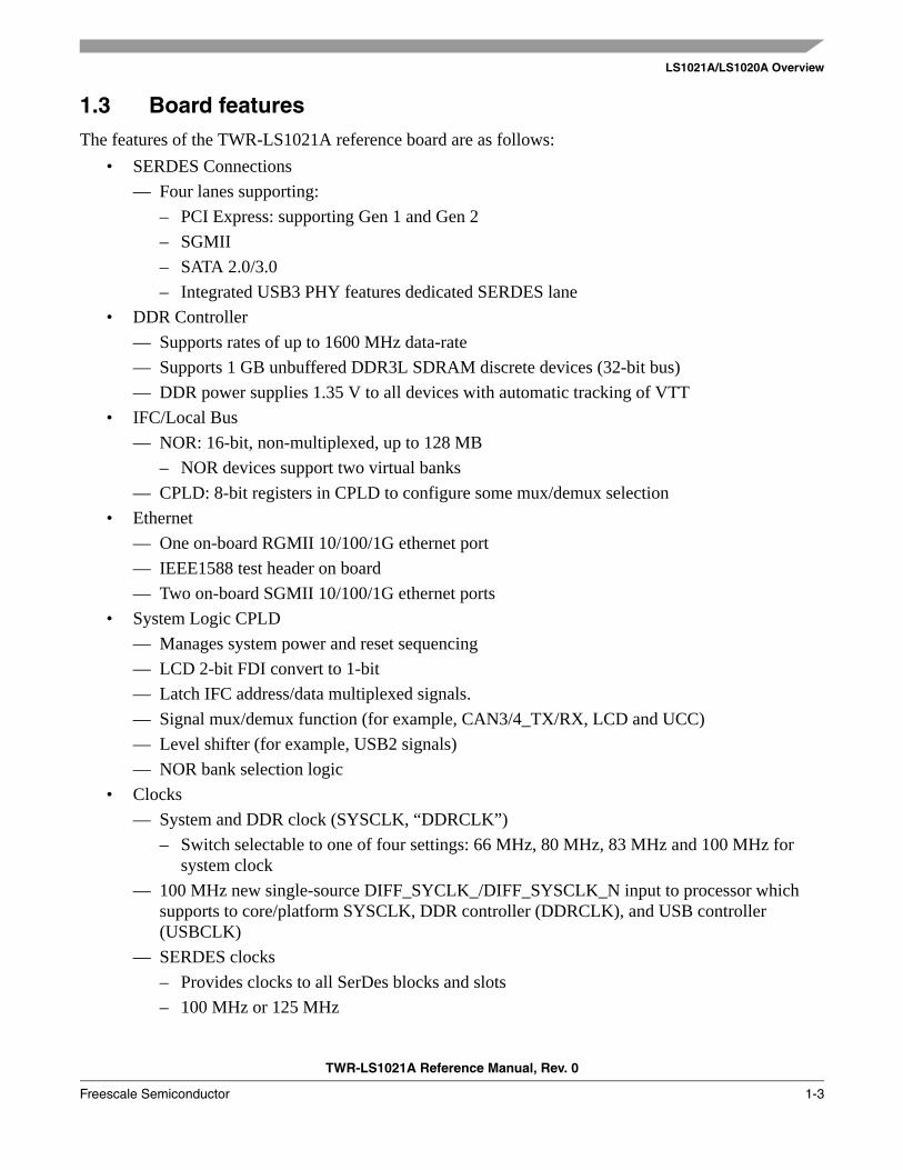
1.4 Block diagramThis section provides a high-level overview of the LS1021A and LS1020A processors, as well as the TWR-LS1021A/LS1020A platform. Figure 1-1 shows the major functional units within the LS1021A device.
LS1021A/LS1020A Overview
TWR-LS1021A Reference Manual, Rev. 0
Freescale Semiconductor 1-5
Figure 1-1. LS1021A block diagram
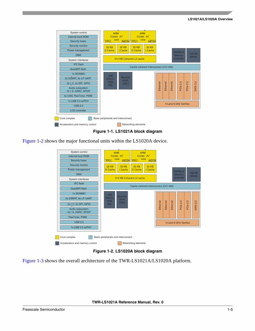
Figure 1-2 shows the major functional units within the LS1020A device.
Figure 1-2. LS1020A block diagram
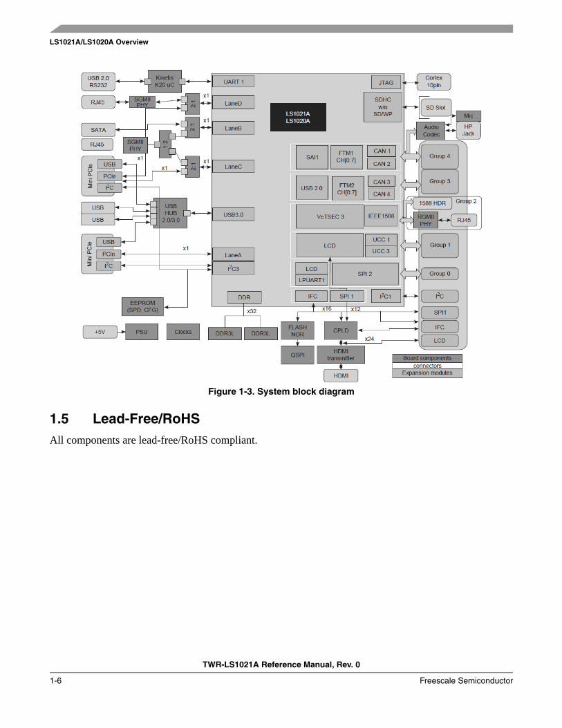
Figure 1-3 shows the overall architecture of the TWR-LS1021A/LS1020A platform.
LS1021A/LS1020A Overview
TWR-LS1021A Reference Manual, Rev. 0
1-6 Freescale Semiconductor
Figure 1-3. System block diagram
1.5 Lead-Free/RoHSAll components are lead-free/RoHS compliant.
Architecture
TWR-LS1021A Reference Manual, Rev. 0
Freescale Semiconductor 2-1
Chapter 2 ArchitectureThe TWR-LS1021A architectures are primarily determined by the processor, and by the need to evaluate as many of its features as possible, maximizing testability without impacting the ability to deliver an easily usable off-the-shelf software development platform.
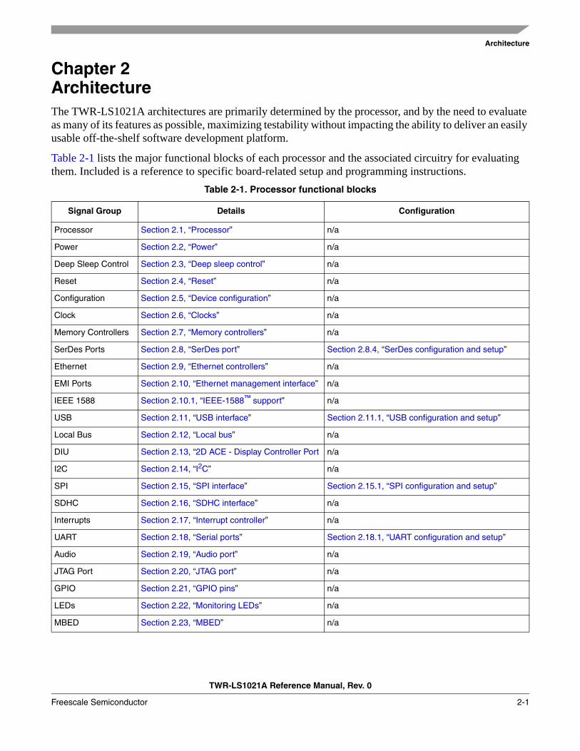
Table 2-1 lists the major functional blocks of each processor and the associated circuitry for evaluating them. Included is a reference to specific board-related setup and programming instructions.
Table 2-1. Processor functional blocks
Signal Group Details Configuration
Processor Section 2.1, “Processor” n/a
Power Section 2.2, “Power” n/a
Deep Sleep Control Section 2.3, “Deep sleep control” n/a
Reset Section 2.4, “Reset” n/a
Configuration Section 2.5, “Device configuration” n/a
Clock Section 2.6, “Clocks” n/a
Memory Controllers Section 2.7, “Memory controllers” n/a
SerDes Ports Section 2.8, “SerDes port” Section 2.8.4, “SerDes configuration and setup”
Ethernet Section 2.9, “Ethernet controllers” n/a
EMI Ports Section 2.10, “Ethernet management interface” n/a
IEEE 1588 Section 2.10.1, “IEEE-1588™ support” n/a
USB Section 2.11, “USB interface” Section 2.11.1, “USB configuration and setup”
Local Bus Section 2.12, “Local bus” n/a
DIU Section 2.13, “2D ACE - Display Controller Port n/a
I2C Section 2.14, “I2C” n/a
SPI Section 2.15, “SPI interface” Section 2.15.1, “SPI configuration and setup”
SDHC Section 2.16, “SDHC interface” n/a
Interrupts Section 2.17, “Interrupt controller” n/a
UART Section 2.18, “Serial ports” Section 2.18.1, “UART configuration and setup”
Audio Section 2.19, “Audio port” n/a
JTAG Port Section 2.20, “JTAG port” n/a
GPIO Section 2.21, “GPIO pins” n/a
LEDs Section 2.22, “Monitoring LEDs” n/a
MBED Section 2.23, “MBED” n/a
Architecture
TWR-LS1021A Reference Manual, Rev. 0
2-2 Freescale Semiconductor
2.1 ProcessorThe TWR-LS1021A supports as many features of the LS1021A as possible, as detailed in the following sections. In addition, TWR-LS1021A provides the ability to accept the pin-compatible LS1020A as well, with changes as noted as necessary. A system with a TWR-LS1020A installed is referred to as a TWR-LS1020A; the boards and supporting hardware are all identical, but the ability to use various features depends on the device used.
Lastly, the TWR-LS1021A accept an interposer which allows early evaluation of boards but has limited features and restrictions. A notable restriction of the interposer is that the P1010 used requires 3.3V on OVDD, forcing IFC and other rails to operate and 3.3V. TWR-LS1021A support this by isolating OVDD-powered signals through external translation devices or the FPGA where required.
2.2 PowerThe power supply system of the TWR-LS1021A systems use power from a desktop power supply to provide the numerous processor and peripheral device supplies required. In addition to meeting required power specifications, the following goals guide the power supply architecture:
• Monolithic power supply for VCC (powering internal cores and platform logic)
• DUT-specific power rails are instrumented such that current measurement is possible
• All power supplies can be sequenced per hardware specifications
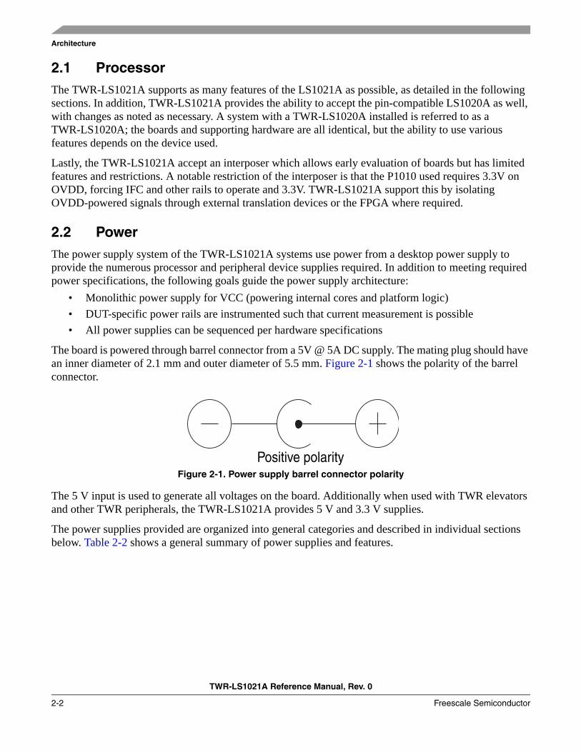
The board is powered through barrel connector from a 5V @ 5A DC supply. The mating plug should have an inner diameter of 2.1 mm and outer diameter of 5.5 mm. Figure 2-1 shows the polarity of the barrel connector.
Figure 2-1. Power supply barrel connector polarity
The 5 V input is used to generate all voltages on the board. Additionally when used with TWR elevators and other TWR peripherals, the TWR-LS1021A provides 5 V and 3.3 V supplies.
The power supplies provided are organized into general categories and described in individual sections below. Table 2-2 shows a general summary of power supplies and features.
Architecture
TWR-LS1021A Reference Manual, Rev. 0
Freescale Semiconductor 2-3
.
2.2.1 VDD/VDDC - Core and platform supply power
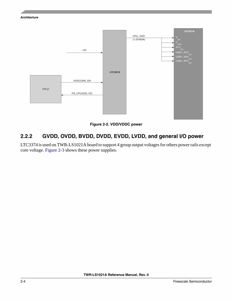
The TWR-LS1021A uses an LTC3616 to provide VDD and VDDC power.
Figure 2-2 shows an overview of this power supply.
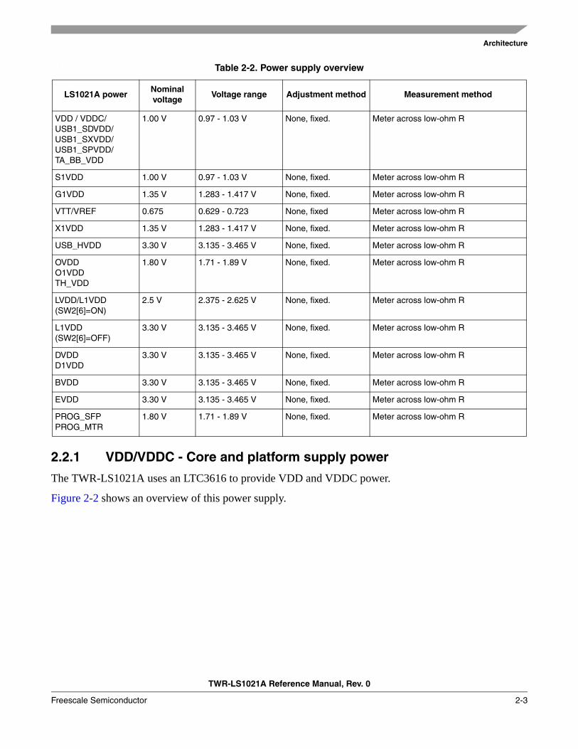
Table 2-2. Power supply overview
LS1021A powerNominal voltage
Voltage range Adjustment method Measurement method
VDD / VDDC/USB1_SDVDD/ USB1_SXVDD/ USB1_SPVDD/ TA_BB_VDD
1.00 V 0.97 - 1.03 V None, fixed. Meter across low-ohm R
S1VDD 1.00 V 0.97 - 1.03 V None, fixed. Meter across low-ohm R
G1VDD 1.35 V 1.283 - 1.417 V None, fixed. Meter across low-ohm R
VTT/VREF 0.675 0.629 - 0.723 None, fixed Meter across low-ohm R
X1VDD 1.35 V 1.283 - 1.417 V None, fixed. Meter across low-ohm R
USB_HVDD 3.30 V 3.135 - 3.465 V None, fixed. Meter across low-ohm R
OVDDO1VDDTH_VDD
1.80 V 1.71 - 1.89 V None, fixed. Meter across low-ohm R
LVDD/L1VDD (SW2[6]=ON)
2.5 V 2.375 - 2.625 V None, fixed. Meter across low-ohm R
L1VDD (SW2[6]=OFF)
3.30 V 3.135 - 3.465 V None, fixed. Meter across low-ohm R
DVDDD1VDD
3.30 V 3.135 - 3.465 V None, fixed. Meter across low-ohm R
BVDD 3.30 V 3.135 - 3.465 V None, fixed. Meter across low-ohm R
EVDD 3.30 V 3.135 - 3.465 V None, fixed. Meter across low-ohm R
PROG_SFPPROG_MTR
1.80 V 1.71 - 1.89 V None, fixed. Meter across low-ohm R
Architecture
TWR-LS1021A Reference Manual, Rev. 0
2-4 Freescale Semiconductor
Figure 2-2. VDD/VDDC power
2.2.2 GVDD, OVDD, BVDD, DVDD, EVDD, LVDD, and general I/O power
LTC3374 is used on TWR-LS1021A board to support 4 group output voltages for others power rails except core voltage. Figure 2-3 shows these power supplies.

Architecture
TWR-LS1021A Reference Manual, Rev. 0
Freescale Semiconductor 2-5
Figure 2-3. GVDD/OVDD/BVDD/DVDD/EVDD/LVDD and general IO power
2.2.3 Fuse programming power
Additionally, fuse programming power is supplied to allow customer programming of ECID fuses; this power is normally off to prevent inadvertent fuse programming.
Figure 2-4 shows the remaining power supplies.
Architecture
TWR-LS1021A Reference Manual, Rev. 0
2-6 Freescale Semiconductor
Figure 2-4. Fuse programming power
2.3 Deep sleep controlNot supported on TWR-LS1021A board.
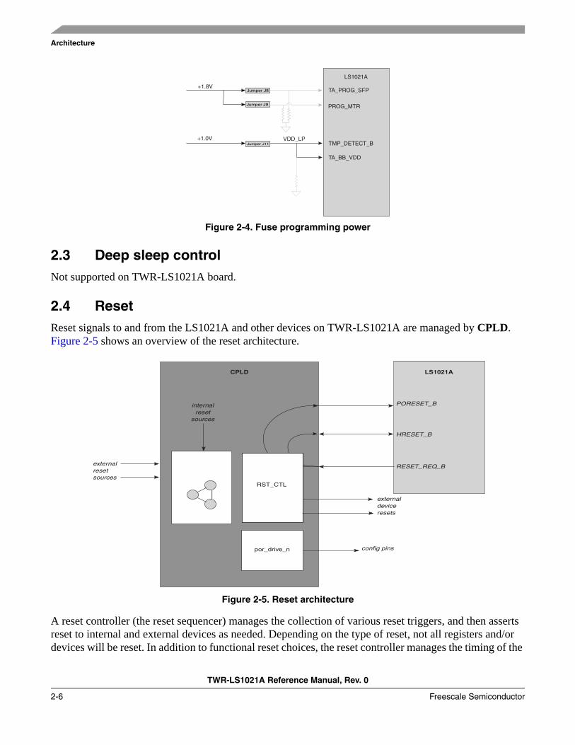
2.4 ResetReset signals to and from the LS1021A and other devices on TWR-LS1021A are managed by CPLD. Figure 2-5 shows an overview of the reset architecture.
Figure 2-5. Reset architecture
A reset controller (the reset sequencer) manages the collection of various reset triggers, and then asserts reset to internal and external devices as needed. Depending on the type of reset, not all registers and/or devices will be reset. In addition to functional reset choices, the reset controller manages the timing of the

Architecture
TWR-LS1021A Reference Manual, Rev. 0
Freescale Semiconductor 2-7
pin-sampled configuration driver logic to insure hardware-spec compliance; Refer Section “(Re)Configuration” for further details.
2.5 Device configurationThe processor uses hardware-sampled pins to configure various portions of the device. The remainder are configured from data in the Reset Configuration Word (RCW).
TWR-LS1021A configuration pins are described in Table 2-3.
2.6 ClocksThe clocks section specify various clocks:
• SYSCLK(single-ended and differential)
• DDRCLK (single-ended)
• SERDES clocks (2 independent options)
• Ethernet clocks
• USB clock
The architecture of the clock section is shown in in Figure 2-6.
Table 2-3. Configuration options
ConfigurationSignal
Nets SampledSwitchPreset
CPLD Register Description
cfg_rcw_src[0:8] IFC_AD[8:15], IFC_CLE
SW2[1:4] 0x05: cfg_rcw_src1[0:7]0x06: cfg_rcw_src2[0]
Specifies RCW fetch location by SW2[1:4] decode.
cfg_dram_type IFC_A[21] n/a n/a Specifies DDR3L or DDR4.Affects GVDD power supply.
cfg_ifc_te IFC_TE n/a n/a IFC TE signal enable; not normally used.
cfg_gpinput[0:7] IFC_AD[0:7] n/a n/a Application defined.
cfg_eng_use0 IFC_WE0_B n/a n/a Differential or single ended clock selection.
cfg_eng_use1 IFC_OE_B n/a n/a Reserved

Architecture
TWR-LS1021A Reference Manual, Rev. 0
2-8 Freescale Semiconductor
Figure 2-6. Clock architecture
2.6.1 SYSCLK / DDRCLK
SYSCLK and DDRCLK are provided by an IDT 6V49205BNLGI, a programmable frequency synthesizer with hardware presets. The device is strapped to provide 100 MHz to SYSCLK and 67 MHz to DDRCLK during power up. LS1021A requires 64 MHz to 100 MHz for both SYSCLK and DDRCLK.
Spread Spectrum Clocking (SSC) options are supported for SYSCLK and DDRCLK by SMBUS. Because SSC reduces the clock rate, reducing the performance somewhat, it is not a preferred operating mode.
Table 2-4. SYSCLK frequency options
FS[0:1] SYSCLK Notes
0 0 66.67 MHz n/a
0 1 80 MHz n/a
1 0 100.00 MHz default
1 1 83.33 MHz n/a
Table 2-5. DDRCLK frequency options
DDRCLK pin DDRCLK Notes
pull-up 66.67 MHz n/a
pull-down 100.00 MHz Default on TWR-LS1021A

Architecture
TWR-LS1021A Reference Manual, Rev. 0
Freescale Semiconductor 2-9
2.6.1.1 Single-Source SYSCLK
A new feature supported on TWR-LS1021A is “single-source” clocking. In this mode, a differential clock is supplied to the DIFF_SYSCLK_P/DIFF_SYSCLK_N inputs to the processor, which is in turn used to supply clocks to the core and platform (SYSCLK), DDR controller (DDRCLK) and USB controller (USBCLK).
2.6.2 SerDes clocks
The LS1021A SerDes port accepts two different differential clock inputs (SD1_REFCLK1 and SD1_REFCLK2), allowing the flexibility to use different protocols with different clock rates on the SerDes pins. The clock inputs are provided by the IDT clock generator device, which can generate the required 100.00 or 125.00 frequencies.
2.6.3 Ethernet and USB clocks
Ethernet clock is also provided by an IDT6V49205BNLGI, which supplies 125.0 MHz to the Ethernet port clock inputs (EC3_GTXCLK_125), as well as to the separate RGMII PHYs. Additionally, a 60 MHz reference clock is provided for the USBCLK input from external USB PHY.
Additionally, for the Ethernet PHY input clocks are individually supplied by IDT6V49205BNLGI as well.
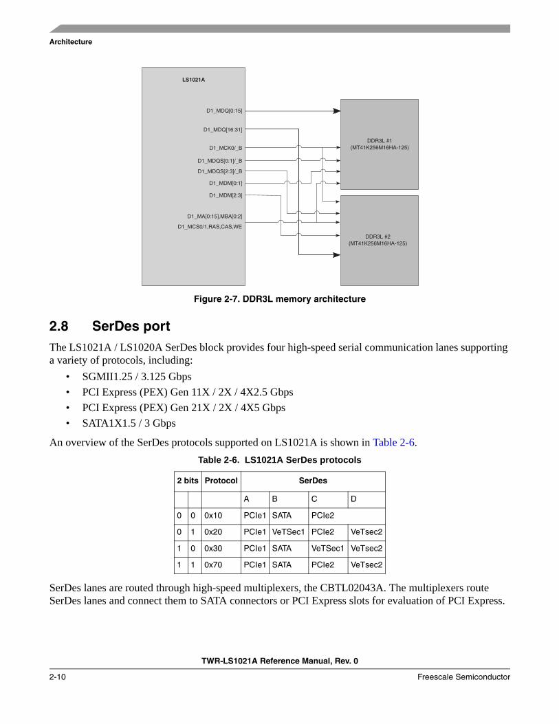
2.7 Memory controllersThe TWR-LS1021A supports high-speed DRAM with 1 GB DDR3L SDRAM discrete devices (32-bit bus). The memory interface includes all the necessary termination and I/O power, and is routed so as to achieve maximum performance of the memory bus, as shown in Figure 2-7.
Architecture
TWR-LS1021A Reference Manual, Rev. 0
2-10 Freescale Semiconductor
Figure 2-7. DDR3L memory architecture
2.8 SerDes portThe LS1021A / LS1020A SerDes block provides four high-speed serial communication lanes supporting a variety of protocols, including:
• SGMII1.25 / 3.125 Gbps
• PCI Express (PEX) Gen 11X / 2X / 4X2.5 Gbps
• PCI Express (PEX) Gen 21X / 2X / 4X5 Gbps
• SATA1X1.5 / 3 Gbps
An overview of the SerDes protocols supported on LS1021A is shown in Table 2-6.
SerDes lanes are routed through high-speed multiplexers, the CBTL02043A. The multiplexers route SerDes lanes and connect them to SATA connectors or PCI Express slots for evaluation of PCI Express.
Table 2-6. LS1021A SerDes protocols
2 bits Protocol SerDes
A B C D
0 0 0x10 PCIe1 SATA PCIe2
0 1 0x20 PCIe1 VeTSec1 PCIe2 VeTsec2
1 0 0x30 PCIe1 SATA VeTSec1 VeTsec2
1 1 0x70 PCIe1 SATA PCIe2 VeTsec2
Architecture
TWR-LS1021A Reference Manual, Rev. 0
Freescale Semiconductor 2-11
Software must map the cfg_srds1_prtcl field in the RCW to the bits shown in Table 2-6 to the selected Serdes configuration. To assist software in this, the CPLD will map either the RCW[cfg_srds1_prtcl] field to these bits (if accessible), or map a DIP switch using the same process, see Section 2.8.4 for details.
2.8.1 PCI Express support
TWR-LS1021A supports evaluation of two PCI Express slots using mini PCI Express Gen-1 or Gen-2 card. In a few specialized cases (0x10 protocol), two PCI Express controllers are routed to one PCI Express slot. This mode is designed for use with a specialized breakout card, and should never be enabled with normal PCI Express cards installed.
For support this specific x2 mini PCI Express, one of connectors has some additional signals. The expansion connector is used to support costumed x2 mini PCIE card.
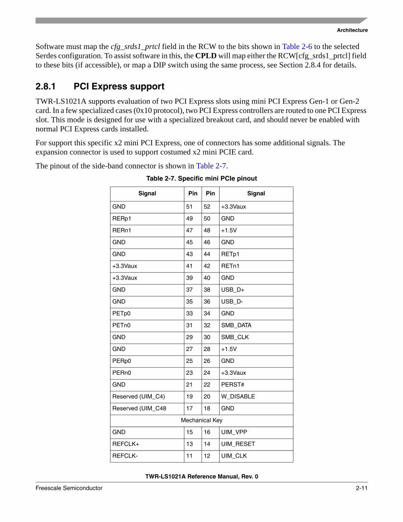
The pinout of the side-band connector is shown in Table 2-7.
Table 2-7. Specific mini PCIe pinout
Signal Pin Pin Signal
GND 51 52 +3.3Vaux
RERp1 49 50 GND
RERn1 47 48 +1.5V
GND 45 46 GND
GND 43 44 RETp1
+3.3Vaux 41 42 RETn1
+3.3Vaux 39 40 GND
GND 37 38 USB_D+
GND 35 36 USB_D-
PETp0 33 34 GND
PETn0 31 32 SMB_DATA
GND 29 30 SMB_CLK
GND 27 28 +1.5V
PERp0 25 26 GND
PERn0 23 24 +3.3Vaux
GND 21 22 PERST#
Reserved (UIM_C4) 19 20 W_DISABLE
Reserved (UIM_C48 17 18 GND
Mechanical Key
GND 15 16 UIM_VPP
REFCLK+ 13 14 UIM_RESET
REFCLK- 11 12 UIM_CLK

Architecture
TWR-LS1021A Reference Manual, Rev. 0
2-12 Freescale Semiconductor
2.8.2 SGMII support
TWR-LS1021A supports evaluation of the SGMII protocol for serialized Ethernet PHYs. Ethernet data is carried over the SerDes lanes. On TWR-LS1021A, two Atheros AR8033 PHY are used to support SGMII mode.
2.8.3 SATA support
SATA could be evaluated an on-board SATA headers. LS1021A could support SATA3.0 protocol with maximum 6 Gbps data rate.
2.8.4 SerDes configuration and setup
The SerDes multiplexers require initialization of several CPLD register bits. CPLD attempts to preset the values based on a DIP switch, which should be set to match the selected RCW[cfg_srds1_prtcl] field. Software can override the presets at any time.
GND 9 10 UIM_DATA
CLKREQ# 7 8 UIM_PWR
COEX2 5 6 1.5V
COEX1 3 4 GND
WAKE# 1 2 3.3Vaux
Table 2-8. SerDes configuration
Configuration Signal
Controls Value Description
none SW: SW3[6]
REG: 0x0D
0 Lane A PCIE#1 (x1)Lane B SGMII 1Lane C PCIE#2 (x1)Lane D SGMII 2
1 Lane A PCIE#1 (x1)Lane B SATA x1Lane C PCIE#2 (x1)Lane D SGMII 2
0 Lane A PCIE#1 (x1)Lane B SGMII 1Lane C PCIE#2 (x1)Lane D SGMII 2
1 Lane A PCIE#1 (x1)Lane B SATA x1Lane C PCIE#2 (x1)Lane D SGMII 2
Table 2-7. Specific mini PCIe pinout
Signal Pin Pin Signal

Architecture
TWR-LS1021A Reference Manual, Rev. 0
Freescale Semiconductor 2-13
2.9 Ethernet controllersThe TWR-LS1021A supports three Ethernet Controllers (EC) which can connect to Ethernet PHYs using MII or RGMII protocols. The EC3 port can operate in RGMII mode and is always on, while the EC2 and EC3 ports only operates in SGMII mode. All three ports connects to Atheros AR8033 PHYs.
Connections and routing for the TSEC are summarized in Table 2-9.
The drives the and associated PHY devices with a 125.00 MHz clock, from one of various sources. See Section 2.6 for details on Ethernet clocking.
2.10 Ethernet management interfaceThe EMI routing architecture is shown in Figure 2-8.
Table 2-9. Ethernet port locations
EC # ModeInterface voltage
PHY address
Connector location Status indicator
1 SGMII S1VDD/X1VDD (1.0V/1.35V)
2 P1 Bottom R: Transmit or Receive activityL: Link (1000M)
2 SGMII S1VDD/X1VDD (1.0V/1.35V)
0 P1 Top R: Transmit or Receive activityL: Link (1000M)
3 RGMII LVDD(2.5V)
1 U20 L: Transmit or Receive activityR: Link (Any speed)

Architecture
TWR-LS1021A Reference Manual, Rev. 0
2-14 Freescale Semiconductor
Figure 2-8. Ethernet MII routing
2.10.1 IEEE-1588™ support
The LS1021A/LS1020A includes support for the IEEE 1588 precision time protocol (PTP). This facility works in tandem with the internal Ethernet controllers to time-stamp incoming packets. This is supported at a basic level with internal logic and the use of a precision 125.00 MHz reference clock, accurate to ±25 ppm. Figure 2-9 shows an overview of the IEEE 1588 block.

Architecture
TWR-LS1021A Reference Manual, Rev. 0
Freescale Semiconductor 2-15
Figure 2-9. IEEE-1588 interface overview
2.11 USB interface
The TWR-LS1021A/LS1020A systems have one integrated USB 3.0 (USB1) and one USB 2.0 (USB2) controllers that allow direct connection to USB ports with appropriate protection circuitry and power supplies. Figure 2-10 shows the USB section.
Figure 2-10. USB architecture
Power for the ports is provided by a Maxim MAX1588, which supplies 5V at up to 1.2A per port. The power enable and power-fault-detect pins are connected directly to the LS1021A/LS1020A for individual port management.

Architecture
TWR-LS1021A Reference Manual, Rev. 0
2-16 Freescale Semiconductor
2.11.1 USB configuration and setup
The USB block requires no board-specific setup or programming.
2.12 Local busThe LS1021A / LS1020A Integrated Flash Controller (IFC), also called the “local bus”, supports 32-bit addressing and 8- or 16-bit data widths, for a variety of devices. Figure 2-12 shows an overview of the IFC bus.
Figure 2-11. IFC architecture
On TWR-LS1021A board, the devices available on the IFC bus include:
Table 2-10. IFC devices
IFC device Mfg. Part number Description
NOR Micron JS28F00AM29EWHA 1Gb (128MB) 110ns parallel NOR flash.
ELEV Freescale TWR-ELEV, TWR-LCD Support TWR-LCD module using IFC bus
CPLD BCSR Freescale n/a Board Control and Status Registers
Architecture
TWR-LS1021A Reference Manual, Rev. 0
Freescale Semiconductor 2-17
2.12.1 IFC chip select
IFC chip select signals are assigned in Table 2-11:
NOTEIFC CS2 and CS3 are multiplexed with I2C3 SCL and SDA, the selection is done in CPLD.
2.12.2 Memory map
Memory addresses are defined by software and rearranged externally by the “cfg_lbmap” functions, there are many possible memory maps. The default memory map shown in Table 2-12 reflects selecting the first line in Table 2-11 (with NOR flash as the boot device).
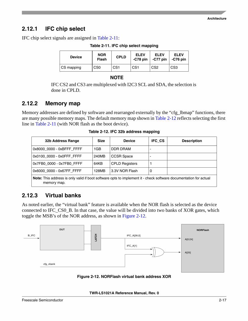
2.12.3 Virtual banks
As noted earlier, the “virtual bank” feature is available when the NOR flash is selected as the device connected to IFC_CS0_B. In that case, the value will be divided into two banks of XOR gates, which toggle the MSB’s of the NOR address, as shown in Figure 2-12.
Figure 2-12. NORFlash virtual bank address XOR
Table 2-11. IFC chip select mapping
DeviceNOR Flash
CPLDELEV
-C78 pinELEV
-C77 pinELEV
-C76 pin
CS mapping CS0 CS1 CS1 CS2 CS3
Table 2-12. IFC 32b address mapping
32b Address Range Size Device IFC_CS Description
0x8000_0000 - 0xBFFF_FFFF 1GB DDR DRAM -
0x0100_0000 - 0x0FFF_FFFF 240MB CCSR Space -
0x7FB0_0000 - 0x7FB0_FFFF 64KB CPLD Registers 1
0x6000_0000 - 0x67FF_FFFF 128MB 3.3V NOR Flash 0
Note: This address is only valid if boot software opts to implement it - check software documentation for actual memory map.
Architecture
TWR-LS1021A Reference Manual, Rev. 0
2-18 Freescale Semiconductor
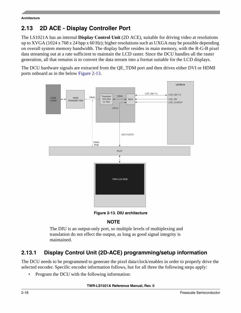
2.13 2D ACE - Display Controller PortThe LS1021A has an internal Display Control Unit (2D ACE), suitable for driving video at resolutions up to XVGA (1024 x 768 x 24 bpp x 60 Hz); higher resolutions such as UXGA may be possible depending on overall system memory bandwidth. The display buffer resides in main memory, with the R-G-B pixel data streaming out at a rate sufficient to maintain the LCD raster. Since the DCU handles all the raster generation, all that remains is to convert the data stream into a format suitable for the LCD displays.
The DCU hardware signals are extracted from the QE_TDM port and then drives either DVI or HDMI ports onboard as in the below Figure 2-13.
Figure 2-13. DIU architecture
NOTEThe DIU is an output-only port, so multiple levels of multiplexing and translation do not effect the output, as long as good signal integrity is maintained.
2.13.1 Display Control Unit (2D-ACE) programming/setup information
The DCU needs to be programmed to generate the pixel data/clock/enables in order to properly drive the selected encoder. Specific encoder information follows, but for all three the following steps apply:
• Program the DCU with the following information:

Architecture
TWR-LS1021A Reference Manual, Rev. 0
Freescale Semiconductor 2-19
— Raster (framebuffer) width, height and depth
— An “Area Of Interest”, often just equal to the display width and height.
• Pixel clock within limits of monitor
• Horizontal and vertical sync parameters, which include:
— Polarity (generally positive, but not always)
— Front/back “porch” - the interval between sync transitions and active pixel data; usually one or two pixel clocks (HSYNC) or one or two lines (VSYNC) is sufficient.
— Sync assertion time - display width (in pixels) + front and back porch (in pixels), plus the sync assertion time, should be approximately equal to the monitor stated horizontal timing parameter (which might be in units of microseconds, pixels or Hz). A similar process is used for vertical timing.
The DCU block are configured as described in Table 2-13.
2.14 I2CThe LS1021A / LS1020A devices support up to four I2C buses.
Figure 2-14 shows the I2C subsystem connection. The devices available on each I2C bus segment are listed in Table 2-14.
Table 2-13. DIU configuration
Configuration signal Controls Value Description
cfg_mux_qetdm_diu0 SW: SW3[6]REG:0x0C
0 QE TDM signals are routed to the DCU block.
1 QE TDM signals are routed to the UCC block.

Architecture
TWR-LS1021A Reference Manual, Rev. 0
2-20 Freescale Semiconductor
Figure 2-14. I2C architecture
I2C bus device addresses are summarized in Table 2-14.
Table 2-14. I2C bus device map
I2C Bus7b
Addr.Description Device Notes
(all) - / I2C Master n/a
I2C2 0x0A Audio Codec SGTL5000 n/a
I2C2 0x39, 0x3D
HDMI Transmitter SiI9022A n/a
I2C2 0x520x53
0x52(256B): SPD;0x53(256B): SystemID
512B EEPROM:CAT24C05
DIMM SPD.Stores board specific data, including MAC addresses, serial number/errata, etc. Write protectable.
I2C2 - miniPCIe1 Slot Slave address depends on miniPCIe cards on the slot.
I2C2 - TWR-ELEV Pin NO. C7, C8 Slave address depends on TWR modules on the ELEV.
I2C1 0x69 Clock generator 6V49205BNLGI n/a

Architecture
TWR-LS1021A Reference Manual, Rev. 0
Freescale Semiconductor 2-21
2.15 SPI interface
The LS1021A / LS1020A serial peripheral interface (SPI) pins may be used for off-board SPI device access: For various SPI memory devices or SPI controller of various TWR modules.
Figure 2-16 shows the overall connections of the two SPI portions.
Figure 2-15. SPI architecture
2.15.1 SPI configuration and setup
CPLD registers and SW selects SPI2 or LCD/LPUART and SPI1 or IFC.
I2C1 0x2C USB HUB USB5534B Default this device is not connected to I2C1 bus.
I2C1 - miniPCIe2 Slot Slave address depends on miniPCIe cards on the slot.
I2C3 0x66, 0x67
CPU Core DCDC monitor LTC2945 n/a
I2C3 - TWR-ELEV Pin NO. A7, A8 Slave address depends on TWR modules on the ELEV.
Note: “7b” addresses do not include the R/W bit as an address member, though some datasheets might do so. For consistency, all I2C addresses are 7 bits of address only.
Table 2-14. I2C bus device map (continued)
I2C Bus7b
Addr.Description Device Notes

Architecture
TWR-LS1021A Reference Manual, Rev. 0
2-22 Freescale Semiconductor
2.16 SDHC interfaceThe LS1021A / LS1020A SDHC interface supports a large variety of devices, both in terms of width as well as the ability to use special signals to accelerate data transfer:
• MMC cards, 1x, 4x or 8x wide, 3.3 V only
• Legacy MMC cards: 1x, 4x or 8x wide, 3.3 V only
• SDHC card, 1x or 4x wide, 3.3 V only
To handle all these options, TWR-LS1021A systems feature a full-size connector which a variety of adapter cards install.
NOTESDHC_WP and SDHC_CD_N are multiplexed with I2C2 signals, so default they are not supported.
Figure 2-16 shows the overall connections of the SDHC portion
Figure 2-16. SDHC architecture
Table 2-15. SPI configuration
Configuration Signal
Controls Value Description
cfg_spi2_lcd SW: SW3[6] 0 LCD/LPUART
1 SPI2
REG: 0x0A 0 SPI2
1 LPUART1
cfg_ifc_spi1 SW: SW2[7] 0 SPI1
1 IFC (or I2C3)
Architecture
TWR-LS1021A Reference Manual, Rev. 0
Freescale Semiconductor 2-23
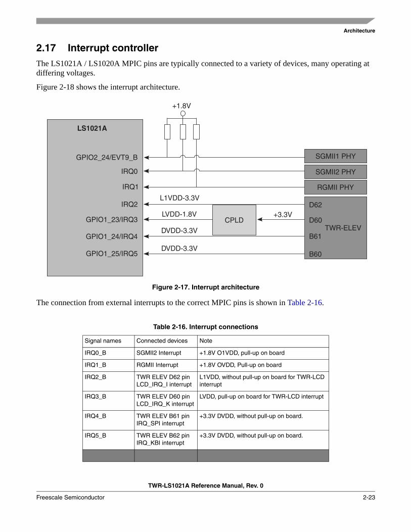
2.17 Interrupt controller The LS1021A / LS1020A MPIC pins are typically connected to a variety of devices, many operating at differing voltages.
Figure 2-18 shows the interrupt architecture.
Figure 2-17. Interrupt architecture
The connection from external interrupts to the correct MPIC pins is shown in Table 2-16.
Table 2-16. Interrupt connections
Signal names Connected devices Note
IRQ0_B SGMII2 Interrupt +1.8V O1VDD, pull-up on board
IRQ1_B RGMII Interrupt +1.8V OVDD, Pull-up on board
IRQ2_B TWR ELEV D62 pin LCD_IRQ_I interrupt
L1VDD, without pull-up on board for TWR-LCD interrupt
IRQ3_B TWR ELEV D60 pin LCD_IRQ_K interrupt
LVDD, pull-up on board for TWR-LCD interrupt
IRQ4_B TWR ELEV B61 pin IRQ_SPI interrupt
+3.3V DVDD, without pull-up on board.
IRQ5_B TWR ELEV B62 pin IRQ_KBI interrupt
+3.3V DVDD, without pull-up on board.

Architecture
TWR-LS1021A Reference Manual, Rev. 0
2-24 Freescale Semiconductor
2.18 Serial portsThe TWR-LS1021A connect LS1021A UART1 2-wire serial ports to MBED circuit and convert UART signals to a mini USB connector as console UART. TWR-LS1021A could support a 4-wire LPUART by TWR modules, in this case, RTS/CTS flow control is supported. Figure 2-19 shows an overview of the serial ports.
Figure 2-18. Serial architecture
To support the 4-wire LPUART, CPLD can select LPUART1 signals from multiplexed SPI2 signals.
2.18.1 UART configuration and setup
The UART configuration controls are described in Table 2-17.
EVT0_B N.A Unused, pull up only.
EVT1_B N.A Unused
EVT2_B N.A Unused
EVT3_B N.A Unused
EVT4_B N.A Unused.
EVT9_B SGMII1 Interrupt +1.8V O1VDD, pull-up on board
Table 2-16. Interrupt connections (continued)
Signal names Connected devices Note

Architecture
TWR-LS1021A Reference Manual, Rev. 0
Freescale Semiconductor 2-25
2.19 Audio portThe SAI (Synchronous Audio Interface) architecture is shown in Figure 2-19.
Figure 2-19. Audio port architecture
Though the LS1021A/LS1020A supports four full duplex Synchronous Audio Interface (SAI) ports up to 30 Mbps each, but only SAI1 is connected to Freescale SGTL5000-32QFN CODECs which drives headphone for I2S, AC97, and Codec/DSP interfaces. Also, SAI1 is routed to HDMI transmitter to supply audio output.
Table 2-17. LPUART1 configuration
Configuration Signal
Controls Value Description
cfg_lpuart1_spi2 SW: SW3[6] 0 LPUART1 pins are selected.
1 SPI2 pins are selected.
REG: 0x0A 0 SPI2 pins are selected.
1 LPUART1 pins are selected.

Architecture
TWR-LS1021A Reference Manual, Rev. 0
2-26 Freescale Semiconductor
2.20 JTAG portThe COP/JTAG architecture is shown in Figure 2-20.
Figure 2-20. JTAG/COP connections
JTAG commands are accepted from the standard COP/JTAG/CCS header and are sent to LS1021A. JTAG could be accessed by external emulator or MBED.
JTAG RST connect to CPLD to generate PORESET signals only at power up.
2.21 GPIO pinsThe LS1021A has no dedicated GPIO pins; instead, GPIO functions are multiplexed internally on other signals, which must be disabled before using the GPIO functions. Because GPIO is not needed for board operation, GPIO evaluation is strictly limited to validation purposes.
In an addition, to remain those GPIO pins primary function, CPLD registers will offer GPIO pin functions for TWR modules control.
Table 2-18. GPIO mapping
DUT Primary Function
DUT GPIO Function
Notes
GPIO GPIO_3[13] Connect to TWR-ELEV pin A10.
GPIO GPIO_3[14] Connect to TWR-ELEV pin B23.
ASLEEP, RTC, etc GPIO_1[13:26] Required for non-GPIO function
Architecture
TWR-LS1021A Reference Manual, Rev. 0
Freescale Semiconductor 2-27
NOTEGPIO I/O signals are actively driven to high or low levels; software can emulate open-drain drivers by driving 0 normally, but driving 1 by switching to input mode and letting the external pullup operate.
2.22 Monitoring LEDsThe TWR-LS1021A has some LEDs which can be used to monitor various functions of the system:
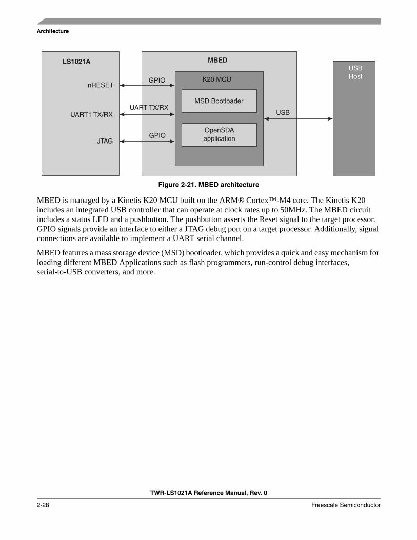
2.23 MBEDThis section will describe MBED circuit on TWR-LS1021A board. MBED is an open-standard serial and debug adapter. It bridges serial and debug communications between a USB host and an embedded target processor as shown in Figure 2-21.
SDHC_CMD, etc GPIO_2[04:27] Required for non-GPIO function
EMI_MDC, etc GPIO_3[00:31] Required for non-GPIO function
EC3_TX_EN, etc GPIO_4[00:28] Required for non-GPIO function
Table 2-19. LED status monitors
LED LED Legend Description COLOR
D1 POWER 3.3V is powered up GREEN
D2 SDA MBED firmware is loaded. GREEN
D5 ASLEEP ASLEEP is being asserted. GREEN
RJ45(U20) right Link RGMII Link GREEN
RJ45(U20) left Activity RGMII Activity YELLOW
RJ45(P1) left down Link SGMII1 Link GREEN
RJ45(P1) right down Activity SGMII1 Activity YELLOW
RJ45(P1) left up Link SGMII2 Link GREEN
RJ45(P1) right up Activity SGMII2 Activity YELLOW
Table 2-18. GPIO mapping (continued)
DUT Primary Function
DUT GPIO Function
Notes
Architecture
TWR-LS1021A Reference Manual, Rev. 0
2-28 Freescale Semiconductor
Figure 2-21. MBED architecture
MBED is managed by a Kinetis K20 MCU built on the ARM® Cortex™-M4 core. The Kinetis K20 includes an integrated USB controller that can operate at clock rates up to 50MHz. The MBED circuit includes a status LED and a pushbutton. The pushbutton asserts the Reset signal to the target processor. GPIO signals provide an interface to either a JTAG debug port on a target processor. Additionally, signal connections are available to implement a UART serial channel.
MBED features a mass storage device (MSD) bootloader, which provides a quick and easy mechanism for loading different MBED Applications such as flash programmers, run-control debug interfaces, serial-to-USB converters, and more.
Tower Elevator Connections
TWR-LS1021A Reference Manual, Rev. 0
Freescale Semiconductor 3-1
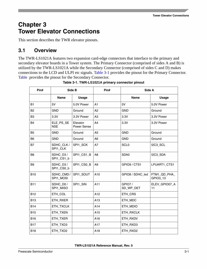
Chapter 3 Tower Elevator ConnectionsThis section describes the TWR elevator pinouts.
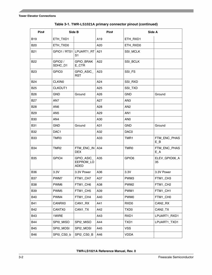
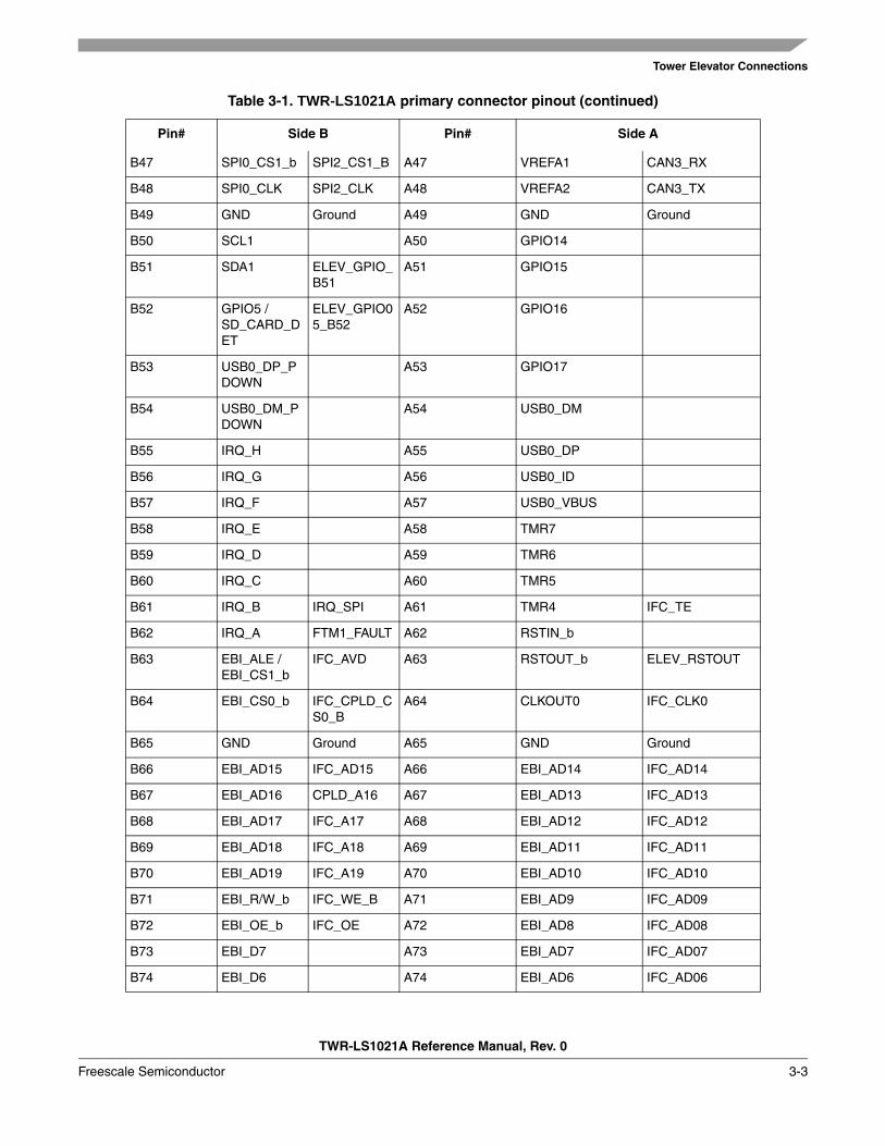
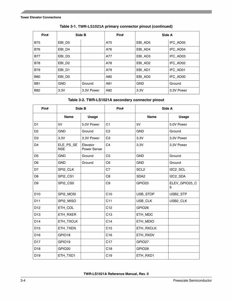
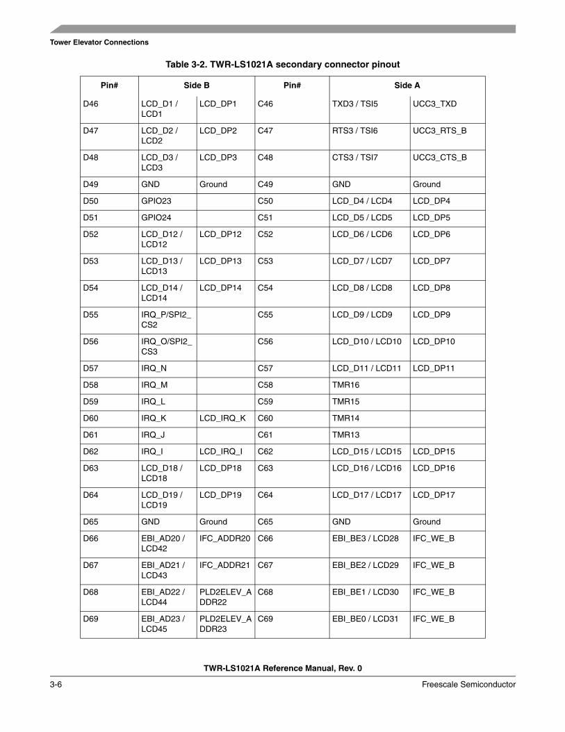
3.1 OverviewThe TWR-LS1021A features two expansion card-edge connectors that interface to the primary and secondary elevator boards in a Tower system. The Primary Connector (comprised of sides A and B) is utilized by the TWR-LS1021A while the Secondary Connector (comprised of sides C and D) makes connections to the LCD and ULPI etc signals. Table 3-1 provides the pinout for the Primary Connector. Table provides the pinout for the Secondary Connector.
Table 3-1. TWR-LS1021A primary connector pinout
Pin# Side B Pin# Side A
Name Usage Name Usage
B1 5V 5.0V Power A1 5V 5.0V Power
B2 GND Ground A2 GND Ground
B3 3.3V 3.3V Power A3 3.3V 3.3V Power
B4 ELE_PS_SENSE
Elevator Power Sense
A4 3.3V 3.3V Power
B5 GND Ground A5 GND Ground
B6 GND Ground A6 GND Ground
B7 SDHC_CLK / SPI1_CLK
SPI1_SCK A7 SCL0 I2C3_SCL
B8 SDHC_D3 / SPI1_CS1_b
SPI1_CS1_B A8 SDA0 I2C3_SDA
B9 SDHC_D3 / SPI1_CS0_b
SPI1_CS0_B A9 GPIO9 / CTS1 LPUART1_CTS1
B10 SDHC_CMD / SPI1_MOSI
SPI1_SOUT A10 GPIO8 / SDHC_led FTM1_QD_PHA_GPIO3_13
B11 SDHC_D0 / SPI1_MISO
SPI1_SIN A11 GPIO7 / SD_WP_DET
ELEV_GPIO07_A11
B12 ETH_COL A12 ETH_CRS
B13 ETH_RXER A13 ETH_MDC
B14 ETH_TXCLK A14 ETH_MDIO
B15 ETH_TXEN A15 ETH_RXCLK
B16 ETH_TXER A16 ETH_RXDV
B17 ETH_TXD3 A17 ETH_RXD3
B18 ETH_TXD2 A18 ETH_RXD2
Tower Elevator Connections
TWR-LS1021A Reference Manual, Rev. 0
3-2 Freescale Semiconductor
B19 ETH_TXD1 A19 ETH_RXD1
B20 ETH_TXD0 A20 ETH_RXD0
B21 GPIO1 / RTS1 LPUART1_RTS1
A21 SSI_MCLK
B22 GPIO2 / SDHC_D1
GPIO_BRAKE_CTR
A22 SSI_BCLK
B23 GPIO3 GPIO_ASIC_RST
A23 SSI_FS
B24 CLKIN0 A24 SSI_RXD
B25 CLKOUT1 A25 SSI_TXD
B26 GND Ground A26 GND Ground
B27 AN7 A27 AN3
B28 AN6 A28 AN2
B29 AN5 A29 AN1
B30 AN4 A30 AN0
B31 GND Ground A31 GND Ground
B32 DAC1 A32 DAC0
B33 TMR3 A33 TMR1 FTM_ENC_PHASE_B
B34 TMR2 FTM_ENC_INDEX
A34 TMR0 FTM_ENC_PHASE_A
B35 GPIO4 GPIO_ASIC_EEPROM_LOADED
A35 GPIO6 ELEV_GPIO06_A35
B36 3.3V 3.3V Power A36 3.3V 3.3V Power
B37 PWM7 FTM1_CH7 A37 PWM3 FTM1_CH3
B38 PWM6 FTM1_CH6 A38 PWM2 FTM1_CH2
B39 PWM5 FTM1_CH5 A39 PWM1 FTM1_CH1
B40 PWM4 FTM1_CH4 A40 PWM0 FTM1_CH0
B41 CANRX0 CAN1_RX A41 RXD0 CAN2_RX
B42 CANTX0 CAN1_TX A42 TXD0 CAN2_TX
B43 1WIRE A43 RXD1 LPUART1_RXD1
B44 SPI0_MISO SPI2_MISO A44 TXD1 LPUART1_TXD1
B45 SPI0_MOSI SPI2_MOSI A45 VSS
B46 SPI0_CS0_b SPI2_CS0_B A46 VDDA
Table 3-1. TWR-LS1021A primary connector pinout (continued)
Pin# Side B Pin# Side A
Tower Elevator Connections
TWR-LS1021A Reference Manual, Rev. 0
Freescale Semiconductor 3-3
B47 SPI0_CS1_b SPI2_CS1_B A47 VREFA1 CAN3_RX
B48 SPI0_CLK SPI2_CLK A48 VREFA2 CAN3_TX
B49 GND Ground A49 GND Ground
B50 SCL1 A50 GPIO14
B51 SDA1 ELEV_GPIO_B51
A51 GPIO15
B52 GPIO5 / SD_CARD_DET
ELEV_GPIO05_B52
A52 GPIO16
B53 USB0_DP_PDOWN
A53 GPIO17
B54 USB0_DM_PDOWN
A54 USB0_DM
B55 IRQ_H A55 USB0_DP
B56 IRQ_G A56 USB0_ID
B57 IRQ_F A57 USB0_VBUS
B58 IRQ_E A58 TMR7
B59 IRQ_D A59 TMR6
B60 IRQ_C A60 TMR5
B61 IRQ_B IRQ_SPI A61 TMR4 IFC_TE
B62 IRQ_A FTM1_FAULT A62 RSTIN_b
B63 EBI_ALE / EBI_CS1_b
IFC_AVD A63 RSTOUT_b ELEV_RSTOUT
B64 EBI_CS0_b IFC_CPLD_CS0_B
A64 CLKOUT0 IFC_CLK0
B65 GND Ground A65 GND Ground
B66 EBI_AD15 IFC_AD15 A66 EBI_AD14 IFC_AD14
B67 EBI_AD16 CPLD_A16 A67 EBI_AD13 IFC_AD13
B68 EBI_AD17 IFC_A17 A68 EBI_AD12 IFC_AD12
B69 EBI_AD18 IFC_A18 A69 EBI_AD11 IFC_AD11
B70 EBI_AD19 IFC_A19 A70 EBI_AD10 IFC_AD10
B71 EBI_R/W_b IFC_WE_B A71 EBI_AD9 IFC_AD09
B72 EBI_OE_b IFC_OE A72 EBI_AD8 IFC_AD08
B73 EBI_D7 A73 EBI_AD7 IFC_AD07
B74 EBI_D6 A74 EBI_AD6 IFC_AD06
Table 3-1. TWR-LS1021A primary connector pinout (continued)
Pin# Side B Pin# Side A
Tower Elevator Connections
TWR-LS1021A Reference Manual, Rev. 0
3-4 Freescale Semiconductor
B75 EBI_D5 A75 EBI_AD5 IFC_AD05
B76 EBI_D4 A76 EBI_AD4 IFC_AD04
B77 EBI_D3 A77 EBI_AD3 IFC_AD03
B78 EBI_D2 A78 EBI_AD2 IFC_AD02
B79 EBI_D1 A79 EBI_AD1 IFC_AD01
B80 EBI_D0 A80 EBI_AD0 IFC_AD00
B81 GND Ground A81 GND Ground
B82 3.3V 3.3V Power A82 3.3V 3.3V Power
Table 3-2. TWR-LS1021A secondary connector pinout
Pin# Side B Pin# Side A
Name Usage Name Usage
D1 5V 5.0V Power C1 5V 5.0V Power
D2 GND Ground C2 GND Ground
D3 3.3V 3.3V Power C3 3.3V 3.3V Power
D4 ELE_PS_SENSE
Elevator Power Sense
C4 3.3V 3.3V Power
D5 GND Ground C5 GND Ground
D6 GND Ground C6 GND Ground
D7 SPI2_CLK C7 SCL2 I2C2_SCL
D8 SPI2_CS1 C8 SDA2 I2C2_SDA
D9 SPI2_CS0 C9 GPIO25 ELEV_GPIO25_C9
D10 SPI2_MOSI C10 USB_STOP USB2_STP
D11 SPI2_MISO C11 USB_CLK USB2_CLK
D12 ETH_COL C12 GPIO26
D13 ETH_RXER C13 ETH_MDC
D14 ETH_TXCLK C14 ETH_MDIO
D15 ETH_TXEN C15 ETH_RXCLK
D16 GPIO18 C16 ETH_RXDV
D17 GPIO19 C17 GPIO27
D18 GPIO20 C18 GPIO28
D19 ETH_TXD1 C19 ETH_RXD1
Table 3-1. TWR-LS1021A primary connector pinout (continued)
Pin# Side B Pin# Side A

Tower Elevator Connections
TWR-LS1021A Reference Manual, Rev. 0
Freescale Semiconductor 3-5
D20 ETH_TXD0 C20 ETH_RXD0
D21 ULPI_NEXT/USB1_DM
USB2_NXT C21 ULPI_DATA0/USB3_DM
USB2_D0
D22 ULPI_DIR/USB1_DP
USB2_DIR C22 ULPI_DATA1/USB3_DP
USB2_D1
D23 UPLI_DATA5/USB2_DM
USB2_D5 C23 ULPI_DATA2/USB4_DM
USB2_D2
D24 ULPI_DATA6/USB2_DP
USB2_D6 C24 ULPI_DATA3/USB4_DP
USB2_D3
D25 ULPI_DATA7 USB2_D7 C25 ULPI_DATA4 USB2_D4
D26 GND Ground C26 GND Ground
D27 LCD_HSYNC / LCD24
LCD_RGB_HSYNC
C27 AN11
D28 LCD_VSYNC / LCD25
LCD_RGB_VSYNC
C28 AN10
D29 AN13 C29 AN9
D30 AN12 C30 AN8
D31 GND Ground C31 GND Ground
D32 LCD_CLK / LCD26
LCD_CLK_OUT
C32 GPIO29 UCC1_DCD
D33 TMR11 C33 TMR9
D34 TMR10 C34 TMR8
D35 GPIO21 C35 GPIO30 UCC3_DCD
D36 3.3V 3.3V Power C36 3.3V 3.3V Power
D37 PWM15 LCD_PWM C37 PWM11
D38 PWM14 C38 PWM10 CLK_IN_QE
D39 PWM13 C39 PWM9
D40 PWM12 C40 PWM8
D41 CANRX1 CAN4_RX C41 RXD2 / TSI0 UCC1_RXD
D42 CANTX1 CAN4_TX C42 TXD2 / TSI1 UCC1_TXD
D43 GPIO22 ELEV_GPIO22_D43
C43 RTS2 / TSI2 UCC1_RTS_B
D44 LCD_OE / LCD27
LCD_DP_DE C44 CTS2 / TSI3 UCC1_CTS_B
D45 LCD_D0 / LCD0
LCD_DP0 C45 RXD3 / TSI4 UCC3_RXD
Table 3-2. TWR-LS1021A secondary connector pinout
Pin# Side B Pin# Side A
Tower Elevator Connections
TWR-LS1021A Reference Manual, Rev. 0
3-6 Freescale Semiconductor
D46 LCD_D1 / LCD1
LCD_DP1 C46 TXD3 / TSI5 UCC3_TXD
D47 LCD_D2 / LCD2
LCD_DP2 C47 RTS3 / TSI6 UCC3_RTS_B
D48 LCD_D3 / LCD3
LCD_DP3 C48 CTS3 / TSI7 UCC3_CTS_B
D49 GND Ground C49 GND Ground
D50 GPIO23 C50 LCD_D4 / LCD4 LCD_DP4
D51 GPIO24 C51 LCD_D5 / LCD5 LCD_DP5
D52 LCD_D12 / LCD12
LCD_DP12 C52 LCD_D6 / LCD6 LCD_DP6
D53 LCD_D13 / LCD13
LCD_DP13 C53 LCD_D7 / LCD7 LCD_DP7
D54 LCD_D14 / LCD14
LCD_DP14 C54 LCD_D8 / LCD8 LCD_DP8
D55 IRQ_P/SPI2_CS2
C55 LCD_D9 / LCD9 LCD_DP9
D56 IRQ_O/SPI2_CS3
C56 LCD_D10 / LCD10 LCD_DP10
D57 IRQ_N C57 LCD_D11 / LCD11 LCD_DP11
D58 IRQ_M C58 TMR16
D59 IRQ_L C59 TMR15
D60 IRQ_K LCD_IRQ_K C60 TMR14
D61 IRQ_J C61 TMR13
D62 IRQ_I LCD_IRQ_I C62 LCD_D15 / LCD15 LCD_DP15
D63 LCD_D18 / LCD18
LCD_DP18 C63 LCD_D16 / LCD16 LCD_DP16
D64 LCD_D19 / LCD19
LCD_DP19 C64 LCD_D17 / LCD17 LCD_DP17
D65 GND Ground C65 GND Ground
D66 EBI_AD20 / LCD42
IFC_ADDR20 C66 EBI_BE3 / LCD28 IFC_WE_B
D67 EBI_AD21 / LCD43
IFC_ADDR21 C67 EBI_BE2 / LCD29 IFC_WE_B
D68 EBI_AD22 / LCD44
PLD2ELEV_ADDR22
C68 EBI_BE1 / LCD30 IFC_WE_B
D69 EBI_AD23 / LCD45
PLD2ELEV_ADDR23
C69 EBI_BE0 / LCD31 IFC_WE_B
Table 3-2. TWR-LS1021A secondary connector pinout
Pin# Side B Pin# Side A

Tower Elevator Connections
TWR-LS1021A Reference Manual, Rev. 0
Freescale Semiconductor 3-7
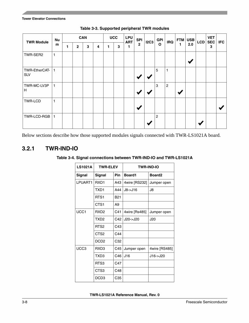
3.2 Supported TWR modulesTWR-LS1021A is compatible the TWR-ELEV pinout. Below table listed supported peripheral modules. Some modules maybe supported but not in the list. The listed modules show LS1021A/LS1020A some important features.
D70 EBI_AD24 / LCD46
PLD2ELEV_ADDR24
C70 EBI_TSIZE0 / LCD32
IFC_BCTL_B
D71 EBI_AD25 / LCD47
PLD2ELEV_ADDR25
C71 EBI_TSIZE1 / LCD33
D72 EBI_AD26 / LCD48
PLD2ELEV_ADDR26
C72 EBI_TS / LCD34 IFC_WE_B
D73 EBI_AD27 / LCD49
PLD2ELEV_ADDR27
C73 EBI_TBST / LCD35 IFC_RB0_B
D74 EBI_AD28 / LCD50
IFC_PAR0 C74 TB_TA / LCD36 IFC_RB1_B
D75 EBI_AD29 / LCD51
IFC_PAR1 C75 EBI_CS4 / LCD37
D76 EBI_AD30 / LCD52
C76 EBI_CS3 / LCD38 IFC_CS3_B
D77 EBI_AD31 / LCD53
C77 EBI_CS2 / LCD39 IFC_CS2_B
D78 LCD_D20 / LCD20
LCD_DP20 C78 EBI_CS1 / LCD40 IFC_CS1_B
D79 LCD_D21 / LCD21
LCD_DP21 C79 GPIO31 / LCD41
D80 LCD_D22 / LCD22
LCD_DP22 C80 LCD_D23 / LCD23 LCD_DP23
D81 GND Ground C81 GND Ground
D82 3.3V 3.3V Power C82 3.3V 3.3V Power
Table 3-3. Supported peripheral TWR modules
TWR ModuleNum
CAN UCC LPUART
1
SPI2
I2C3GPIO
IRQFTM
1USB2.0
LCDVETSEC
3IFC
1 2 3 4 1 3
TWR-IND-IO 1st 1
2nd
Table 3-2. TWR-LS1021A secondary connector pinout
Pin# Side B Pin# Side A
Tower Elevator Connections
TWR-LS1021A Reference Manual, Rev. 0
3-8 Freescale Semiconductor
Below sections describe how those supported modules signals connected with TWR-LS1021A board.
3.2.1 TWR-IND-IO
TWR-SER2 1
TWR-EtherCAT-SLV
1 5 1
TWR-MC-LV3PH
1 3 2
TWR-LCD 1
TWR-LCD-RGB 1 2
Table 3-4. Signal connections between TWR-IND-IO and TWR-LS1021A
LS1021A TWR-ELEV TWR-IND-IO
Signal Signal Pin Board1 Board2
LPUART1 RXD1 A43 4wire [RS232] Jumper open
TXD1 A44 J8->J16 J8
RTS1 B21
CTS1 A9
UCC1 RXD2 C41 4wire [Rs485] Jumper open
TXD2 C42 J20->J20 J20
RTS2 C43
CTS2 C44
DCD2 C32
UCC3 RXD3 C45 Jumper open 4wire [RS485]
TXD3 C46 J16 J16->J20
RTS3 C47
CTS3 C48
DCD3 C35
Table 3-3. Supported peripheral TWR modules
TWR ModuleNum
CAN UCC LPUART
1
SPI2
I2C3GPIO
IRQFTM
1USB2.0
LCDVETSEC
3IFC
1 2 3 4 1 3

Tower Elevator Connections
TWR-LS1021A Reference Manual, Rev. 0
Freescale Semiconductor 3-9
3.2.2 TWR-SER2
3.2.3 TWR-EtherCAT-SLV
CAN1 CAN0_RX B41 NP-R10, R11 CAN PHY0
CAN0_TX B42 Pop R10, R11
CAN2 RXD0 A41 Jumper open CAN PHY1
TXD0 A42 J9 J9->J15
CAN3 CAN1_RX A47 CAN PHY0 US-SH1, SH2
CAN1_RX A48 MS-SH1, SH2
CAN4 CAN2_RX D41 CAN PHY1 Jumper open
CAN2_TX D42 J15 J9
GPIO RSTOUT A63 Reset board
Table 3-5. Signal connections between TWR-SER2 and TWR-LS1021A
LS1021A TWR-ELEV TWR-SER2
Signal Signal Pin Signal Function
USB 2.0 ULPI_NEXT D21 ULPI_NEXT USB330 PHY
ULPI_DIR D22 ULPI_DIR
ULPI_STOP C10 ULPI_STOP
ULPI_CLK C11 UPLI_CLK
UPLI_DATA0 C21 ULPI_DATA0
ULPI_DATA1 C22 ULPI_DATA1
ULPI_DATA2 C23 ULPI_DATA2
ULPI_DATA3 C24 ULPI_DATA3
ULPI_DATA4 C25 ULPI_DATA4
ULPI_DATA5 C23 ULPI_DATA5
ULPI_DATA6 D21 ULPI_DATA6
ULPI_DATA7 D25 ULPI_DATA7
Table 3-6. Signal connections between TWR-EtherCAT-SLV and TWR-LS1021A
LS1021A TWR-ELEV TWR-EtherCAT-SLV
Signal Signal Pin Signal Function
Table 3-4. Signal connections between TWR-IND-IO and TWR-LS1021A (continued)
LS1021A TWR-ELEV TWR-IND-IO

Tower Elevator Connections
TWR-LS1021A Reference Manual, Rev. 0
3-10 Freescale Semiconductor
3.2.4 TWR-MC-LV3PH
I2C3 SCL0 A7 I2C EEPROM (Config)
SDA0 A8
SPI2 SPIO_MISO B44 SPI Data interface to FPGA
SPI0_MOSI B45
SPI0_CS0_B B46
SPI0_CS1B B47
SPI0_CLK B48
IRQ IRQ_B B61 SPI.IRQ
LPUART/SPI CTS1 A9 ASIC_LATCH1
RTS1 B21 B21 ASIC_LATCH0
GPIO GPIO3 B23 ASIC_RESET
GPIO4 B35 ASIC_EEPROM_LOADED
GPIO6 A35 ERR LED
GPIO2 B22 GPIO0 NC
SCL1 B51 GPIO1
GPIO8 A10 GPIO2 LATCH0
GPIO7 A11 GPIO3 LATCH1
Table 3-7. Signal connections between TWR-MC-LV3PH and TWR-LS1021A
LS1021A TWR-ELEV TWR-MC-LV3PH TWR-ADCDAC-LTC
Signal Signals Pin Signals Function Signals Function
FTM1 PWM0 A40 PWM_AT
PWM1 A39 PWM_AB
PWM2 A38 PWM_BT
PWM3 A37 PWM_BB
PWM4 B40 PWM_CT
PWM5 B39 PWM_CB
Table 3-6. Signal connections between TWR-EtherCAT-SLV and TWR-LS1021A
LS1021A TWR-ELEV TWR-EtherCAT-SLV
Tower Elevator Connections
TWR-LS1021A Reference Manual, Rev. 0
Freescale Semiconductor 3-11
3.2.5 TWR-LCD
SPI2 SPI0_MISO B44 MISO SPI0_MISO J13.1-2
SPI0_MOSI B45 MOSI SPI0_MOSI J12.1-2
SPI0_CS0 B46 /SS R95, DNP, use CS1 SPI0_CS0 J10.1-2, use CS0
SPI0_CS1 B47 /SS SPI0_CS1 J25, J14, J15, J16.1-2
SPI0_CLK B48 SCLK SPI0_CLK J9.1-2
FTM1 TMR0 A34 ENC_PHASE_A
TMR1 A33 ENC_PHASE_B
TMR2 B34 ENC_INDEX
AN0 A30 I_SENSE_A/ BEMF_SENSE_A U7_CH0 Connect to J27
AN1 A29 I_SENSE_B/ BEMF_SENSE_B U7_CH1
AN2 A28 I_SENSE_C/ BEMF_SENSE_C U7_CH2
AN6 B28 I_SENSE_C/ I_SENSE_DCB U7_CH3
GPIO GPIO1/ RTS1
B21 USER_LED
GPIO2/SDHC_D1
B22 BRAKE_CONTROL
GPIO5/ SD_CARD_DET
B52 DRV_EN
RSTOUT_b A63 RESET
IRQ IRQ_B B61 DRV_INT
IRQ_A B62 DRV_OC
Table 3-8. Signal connections between TWR-LCD and TWR-LS1021A
LS1021A TWR-ELEV TWR-LCD
Signal Signals Pin Signals Function
Table 3-7. Signal connections between TWR-MC-LV3PH and TWR-LS1021A
LS1021A TWR-ELEV TWR-MC-LV3PH TWR-ADCDAC-LTC

Tower Elevator Connections
TWR-LS1021A Reference Manual, Rev. 0
3-12 Freescale Semiconductor
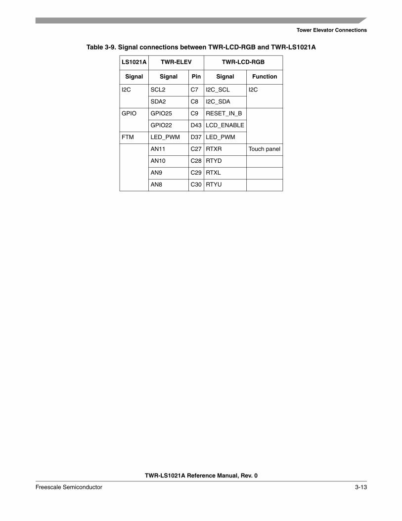
3.2.6 TWR-LCD-RGB
The TWR-LCD-RGB features a 4.3” WQVGA TFT LCD Display (480H x 272 V pixels, 24-bit RGB (8-bit per signal)) with touch sensitive overlay. The LCD interfaces to the Tower System through a 24-bit RGB interface. The 4-wire resistive touch overlay can interface directly with a compatible Tower Processor Module using GPIO enabled ADC lines, or can offload the resistive touch sensing to the on-board Xtrinsic Touch Sensing Platform (CRTouch). CPLD translate from FDI 2-bits to 1-bit.
IFC EBI_AD15 B66 FB_AD15 EBI Bus
EBI_AD14 A66 FB_AD14
EBI_AD13 A67 FB_AD13
EBI_AD12 A68 FB_AD12
EBI_AD11 A69 FB_AD11
EBI_AD10 A70 FB_AD10
EBI_AD9 A71 FB_AD9
EBI_AD8 A72 FB_AD8
EBI_AD7 A73 FB_AD7
EBI_AD6 A74 FB_AD6
EBI_AD5 A75 FB_AD5
EBI_AD4 A76 FB_AD4
EBI_AD3 A77 FB_AD3
EBI_AD2 A78 FB_AD2
EBI_AD1 A79 FB_AD1
EBI_AD0 A80 FB_AD0
EBI_R/W_B B71 FB_R/W_B
EBI_AD16 B67 JM_DC
SPI2 SPI0_MISO B44 JM_MISO SPI
SPI0_MOSI B45 JM_MOSI
SPI0_CLK B48 KM_SCK
SPI0_CS0_B B46
SPI0_CS1_B B47 JM_CSn
AN4 B30 XPLS Touch panel
AN5 B29 YMNS
AN6 B28 XMNS
AN7 B27 YPLS
Table 3-8. Signal connections between TWR-LCD and TWR-LS1021A
LS1021A TWR-ELEV TWR-LCD
Tower Elevator Connections
TWR-LS1021A Reference Manual, Rev. 0
Freescale Semiconductor 3-13
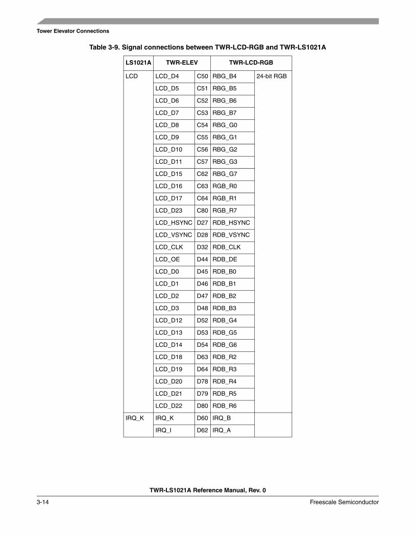
Table 3-9. Signal connections between TWR-LCD-RGB and TWR-LS1021A
LS1021A TWR-ELEV TWR-LCD-RGB
Signal Signal Pin Signal Function
I2C SCL2 C7 I2C_SCL I2C
SDA2 C8 I2C_SDA
GPIO GPIO25 C9 RESET_IN_B
GPIO22 D43 LCD_ENABLE
FTM LED_PWM D37 LED_PWM
AN11 C27 RTXR Touch panel
AN10 C28 RTYD
AN9 C29 RTXL
AN8 C30 RTYU
Tower Elevator Connections
TWR-LS1021A Reference Manual, Rev. 0
3-14 Freescale Semiconductor
LCD LCD_D4 C50 RBG_B4 24-bit RGB
LCD_D5 C51 RBG_B5
LCD_D6 C52 RBG_B6
LCD_D7 C53 RBG_B7
LCD_D8 C54 RBG_G0
LCD_D9 C55 RBG_G1
LCD_D10 C56 RBG_G2
LCD_D11 C57 RBG_G3
LCD_D15 C62 RBG_G7
LCD_D16 C63 RGB_R0
LCD_D17 C64 RGB_R1
LCD_D23 C80 RGB_R7
LCD_HSYNC D27 RDB_HSYNC
LCD_VSYNC D28 RDB_VSYNC
LCD_CLK D32 RDB_CLK
LCD_OE D44 RDB_DE
LCD_D0 D45 RDB_B0
LCD_D1 D46 RDB_B1
LCD_D2 D47 RDB_B2
LCD_D3 D48 RDB_B3
LCD_D12 D52 RDB_G4
LCD_D13 D53 RDB_G5
LCD_D14 D54 RDB_G6
LCD_D18 D63 RDB_R2
LCD_D19 D64 RDB_R3
LCD_D20 D78 RDB_R4
LCD_D21 D79 RDB_R5
LCD_D22 D80 RDB_R6
IRQ_K IRQ_K D60 IRQ_B
IRQ_I D62 IRQ_A
Table 3-9. Signal connections between TWR-LCD-RGB and TWR-LS1021A
LS1021A TWR-ELEV TWR-LCD-RGB

CPLD System Controller Architecture
TWR-LS1021A Reference Manual, Rev. 0
Freescale Semiconductor 4-1
Chapter 4 CPLD System Controller ArchitectureFigure 4-1 shows a detailed block diagram of the CPLD.
Figure 4-1. CPLD overview
4.1 CPLD key featuresThis CPLD includes the following features:
• Control power on sequence

CPLD System Controller Architecture
TWR-LS1021A Reference Manual, Rev. 0
4-2 Freescale Semiconductor
— Power on CPU VDD, GVDD, and others powers.
• Reset signal generation and distribution. System reset features are:
— Power on reset for LS1021A, flash, PCIe, DDR, and PHY devices with initialization of all CPLD registers to default value.
— Manual reset: System will reset and initialize all CPLD registers to default value after pressing reset button.
— Global register reset: Set register to reset the whole system with initializing all CPLD registers to default value.
— Local register reset: Set register to reset the whole system and reserve all CPLD registers current value.
• Control POR Sequence
— Configure POR signals according to external DIP switches or board request.
• Select Multiplexed pins
— Mux I2C and IFC CS2, CS3
— Mux SPI2 and LPUART or LCD
— Mux CAN3 and USB2
— Mux QE and LCD
— Mux SerDes configurations
• IFC Bus
— Latch out address lines from mutiplexed signals and address lines.
— Read/Write CPLD BCSR registers.
— Configure address lines to ELEV local bus pins.
• NOR Bank Selection
— Split NOR flash to two banks.
• LCD FDI translator
— Translate 2-bit FDI signals to 1-bit FDI signals.
4.2 ResetThe reset controller manages not only asserting reset to LS1021A, but to the rest of the system as well. It also maintains the assertion timing of the configuration drive signal (cfg_drv), which causes the CPLD to drive configuration values onto pin-sampled nets.
The following Figure 4-2 shows the reset sequences.

CPLD System Controller Architecture
TWR-LS1021A Reference Manual, Rev. 0
Freescale Semiconductor 4-3
Figure 4-2. Reset power sequencing
4.3 CPLD register map
4.3.1 Memory map
CPLD registers are memory mapped to LS1021A using IFC. Table 4-1 lists the peripheral data bus width and memory map.
Table 4-1. CPLD memory map
4.3.2 BCSR registers map
The BCSR (Board and Control Register) contains many registers that are accessible from device over IFC.
Table 4-2 summarizes the all CPLD registers and Table 4-3 shows a detailed address map description.
Address CS Bank size Device Data width Access
0x7fb00000-0x7fb0ffff CS1 64 KB CPLD 8-bit Read/Write
Table 4-2. CPLD BCSR register block map
Base Address Offset
Access Type
Register Name
0x00 R cpld_ver
0x01 R cpld_ver_sub
0x02 R pcba_ver
0x03 R/W system_rst
0x04 R/W soft_mux_on1

CPLD System Controller Architecture
TWR-LS1021A Reference Manual, Rev. 0
4-4 Freescale Semiconductor
0x05 R/W cfg_rcw_src1
0x06 R/W cfg_rcw_src2
0x07 R/W vbank
0x08 R/W gpio
0x09 R/W i2c3_ifc_mux
0x0A R/W mux_spi2
0x0B R/W can3_usb2_mux
0x0C R/W qe_lcd_mux
0x0D R/W serdes_mux
0x0E R/W global_rst
0x0F R/W elec_cs
0x10 R lvdd_vsel
0x11 R/W soft_mux_on2
0x12 R/W nor_qspi_mux
Table 4-3. CPLD BCSR register detail map
Base Address Offset
Access Type
Description Register Name Default Value
0x00 R Bit [3:0]: CPLD Major Revision RegisterBit [7:4]: Reserved
cpld_ver 0x02
0x01 R Bit [3:0]: CPLD Minor Revision RegisterBit [7:4]: Reserved
cpld_ver_sub 0x00
0x02 R Bit [3:0]: PCBA Revision RegisterBit [7:4]: Reserved
pcba_ver 0x03
0x03 R/W Writing this register to reset system with reserving CPLDregisters value and overriding physical switches on the boardBit [0]: 0 system running(Default)1 system resetBit [7:1]: Reserved
system_rst 0x00
Table 4-2. CPLD BCSR register block map
Base Address Offset
Access Type
Register Name
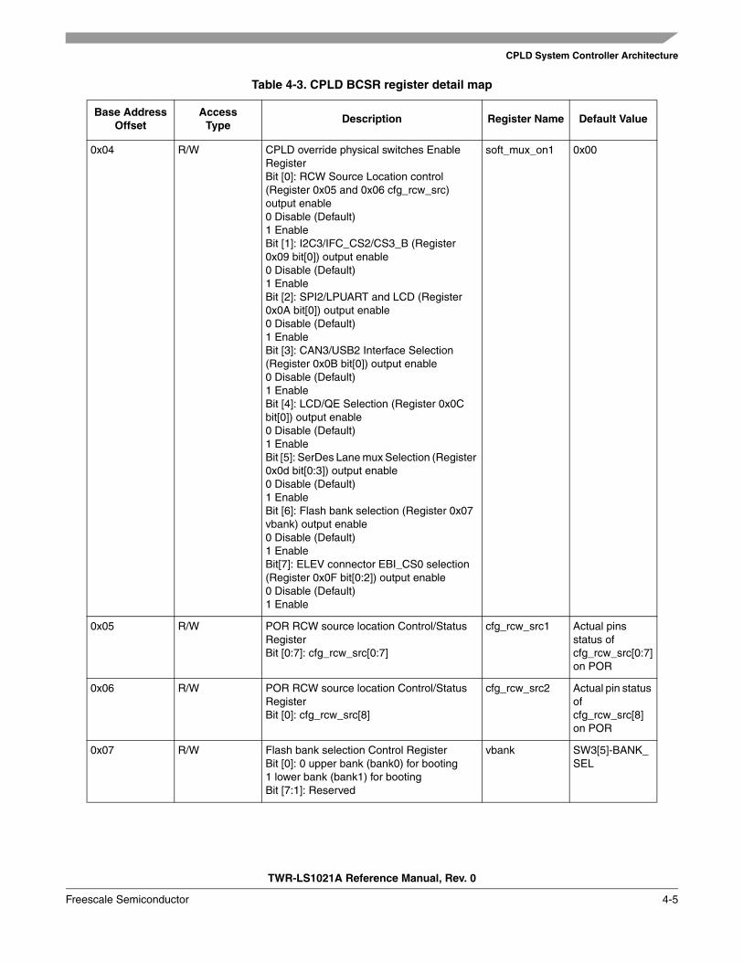
CPLD System Controller Architecture
TWR-LS1021A Reference Manual, Rev. 0
Freescale Semiconductor 4-5
0x04 R/W CPLD override physical switches Enable RegisterBit [0]: RCW Source Location control (Register 0x05 and 0x06 cfg_rcw_src) output enable0 Disable (Default)1 EnableBit [1]: I2C3/IFC_CS2/CS3_B (Register 0x09 bit[0]) output enable0 Disable (Default)1 EnableBit [2]: SPI2/LPUART and LCD (Register 0x0A bit[0]) output enable0 Disable (Default)1 EnableBit [3]: CAN3/USB2 Interface Selection (Register 0x0B bit[0]) output enable0 Disable (Default)1 EnableBit [4]: LCD/QE Selection (Register 0x0C bit[0]) output enable0 Disable (Default)1 EnableBit [5]: SerDes Lane mux Selection (Register 0x0d bit[0:3]) output enable0 Disable (Default)1 EnableBit [6]: Flash bank selection (Register 0x07 vbank) output enable0 Disable (Default)1 EnableBit[7]: ELEV connector EBI_CS0 selection (Register 0x0F bit[0:2]) output enable0 Disable (Default)1 Enable
soft_mux_on1 0x00
0x05 R/W POR RCW source location Control/Status RegisterBit [0:7]: cfg_rcw_src[0:7]
cfg_rcw_src1 Actual pins status of cfg_rcw_src[0:7] on POR
0x06 R/W POR RCW source location Control/Status RegisterBit [0]: cfg_rcw_src[8]
cfg_rcw_src2 Actual pin status of cfg_rcw_src[8] on POR
0x07 R/W Flash bank selection Control RegisterBit [0]: 0 upper bank (bank0) for booting1 lower bank (bank1) for bootingBit [7:1]: Reserved
vbank SW3[5]-BANK_SEL
Table 4-3. CPLD BCSR register detail map
Base Address Offset
Access Type
Description Register Name Default Value
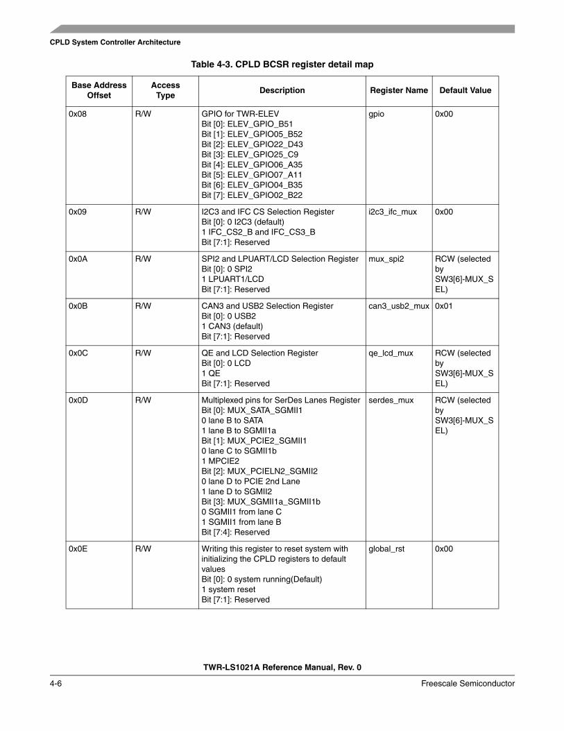
CPLD System Controller Architecture
TWR-LS1021A Reference Manual, Rev. 0
4-6 Freescale Semiconductor
0x08 R/W GPIO for TWR-ELEVBit [0]: ELEV_GPIO_B51Bit [1]: ELEV_GPIO05_B52Bit [2]: ELEV_GPIO22_D43Bit [3]: ELEV_GPIO25_C9Bit [4]: ELEV_GPIO06_A35Bit [5]: ELEV_GPIO07_A11Bit [6]: ELEV_GPIO04_B35Bit [7]: ELEV_GPIO02_B22
gpio 0x00
0x09 R/W I2C3 and IFC CS Selection RegisterBit [0]: 0 I2C3 (default)1 IFC_CS2_B and IFC_CS3_BBit [7:1]: Reserved
i2c3_ifc_mux 0x00
0x0A R/W SPI2 and LPUART/LCD Selection RegisterBit [0]: 0 SPI21 LPUART1/LCDBit [7:1]: Reserved
mux_spi2 RCW (selected by SW3[6]-MUX_SEL)
0x0B R/W CAN3 and USB2 Selection RegisterBit [0]: 0 USB21 CAN3 (default)Bit [7:1]: Reserved
can3_usb2_mux 0x01
0x0C R/W QE and LCD Selection RegisterBit [0]: 0 LCD1 QEBit [7:1]: Reserved
qe_lcd_mux RCW (selected by SW3[6]-MUX_SEL)
0x0D R/W Multiplexed pins for SerDes Lanes RegisterBit [0]: MUX_SATA_SGMII10 lane B to SATA1 lane B to SGMII1aBit [1]: MUX_PCIE2_SGMII10 lane C to SGMII1b1 MPCIE2 Bit [2]: MUX_PCIELN2_SGMII20 lane D to PCIE 2nd Lane1 lane D to SGMII2Bit [3]: MUX_SGMII1a_SGMII1b0 SGMII1 from lane C1 SGMII1 from lane BBit [7:4]: Reserved
serdes_mux RCW (selected by SW3[6]-MUX_SEL)
0x0E R/W Writing this register to reset system with initializing the CPLD registers to default valuesBit [0]: 0 system running(Default)1 system resetBit [7:1]: Reserved
global_rst 0x00
Table 4-3. CPLD BCSR register detail map
Base Address Offset
Access Type
Description Register Name Default Value
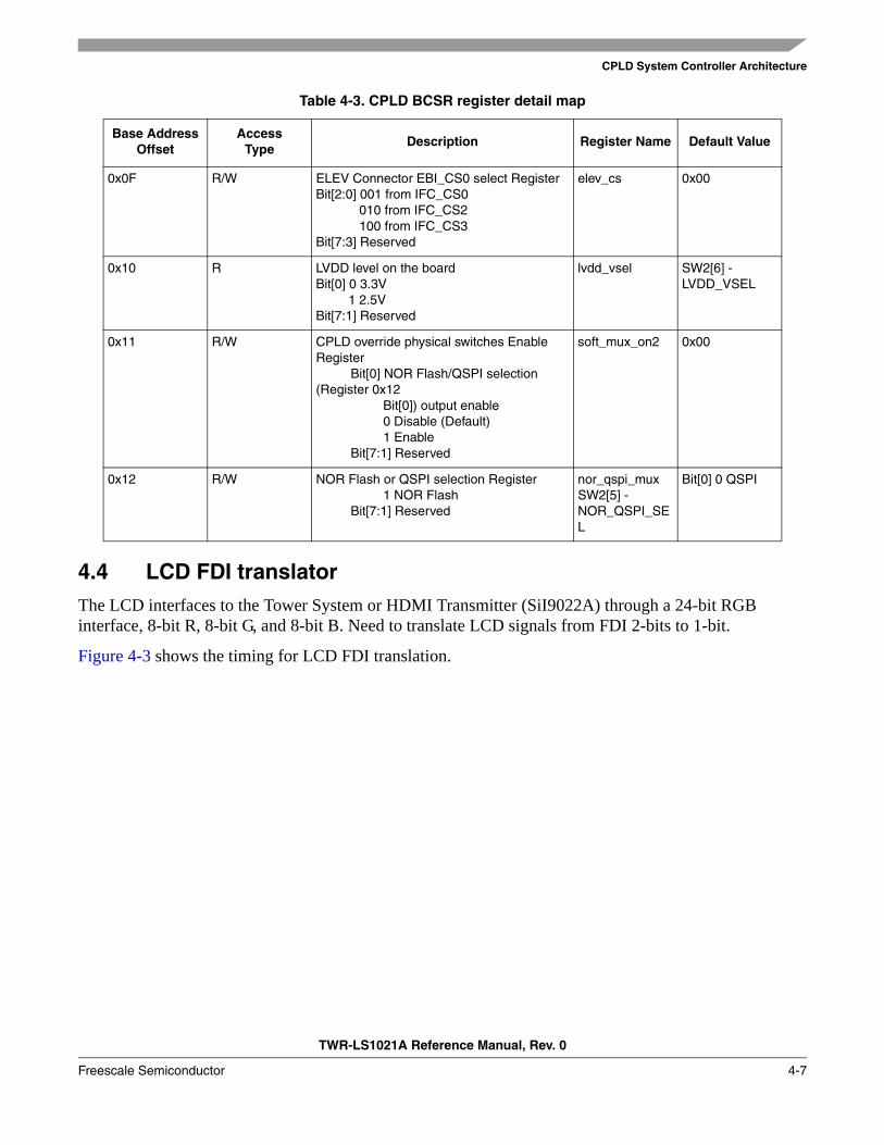
CPLD System Controller Architecture
TWR-LS1021A Reference Manual, Rev. 0
Freescale Semiconductor 4-7
4.4 LCD FDI translatorThe LCD interfaces to the Tower System or HDMI Transmitter (SiI9022A) through a 24-bit RGB interface, 8-bit R, 8-bit G, and 8-bit B. Need to translate LCD signals from FDI 2-bits to 1-bit.
Figure 4-3 shows the timing for LCD FDI translation.
0x0F R/W ELEV Connector EBI_CS0 select RegisterBit[2:0] 001 from IFC_CS0 010 from IFC_CS2 100 from IFC_CS3Bit[7:3] Reserved
elev_cs 0x00
0x10 R LVDD level on the boardBit[0] 0 3.3V 1 2.5VBit[7:1] Reserved
lvdd_vsel SW2[6] - LVDD_VSEL
0x11 R/W CPLD override physical switches Enable Register
Bit[0] NOR Flash/QSPI selection (Register 0x12
Bit[0]) output enable 0 Disable (Default) 1 EnableBit[7:1] Reserved
soft_mux_on2 0x00
0x12 R/W NOR Flash or QSPI selection Register 1 NOR FlashBit[7:1] Reserved
nor_qspi_muxSW2[5] - NOR_QSPI_SEL
Bit[0] 0 QSPI
Table 4-3. CPLD BCSR register detail map
Base Address Offset
Access Type
Description Register Name Default Value

CPLD System Controller Architecture
TWR-LS1021A Reference Manual, Rev. 0
4-8 Freescale Semiconductor
Figure 4-3. Timing of FDI translation
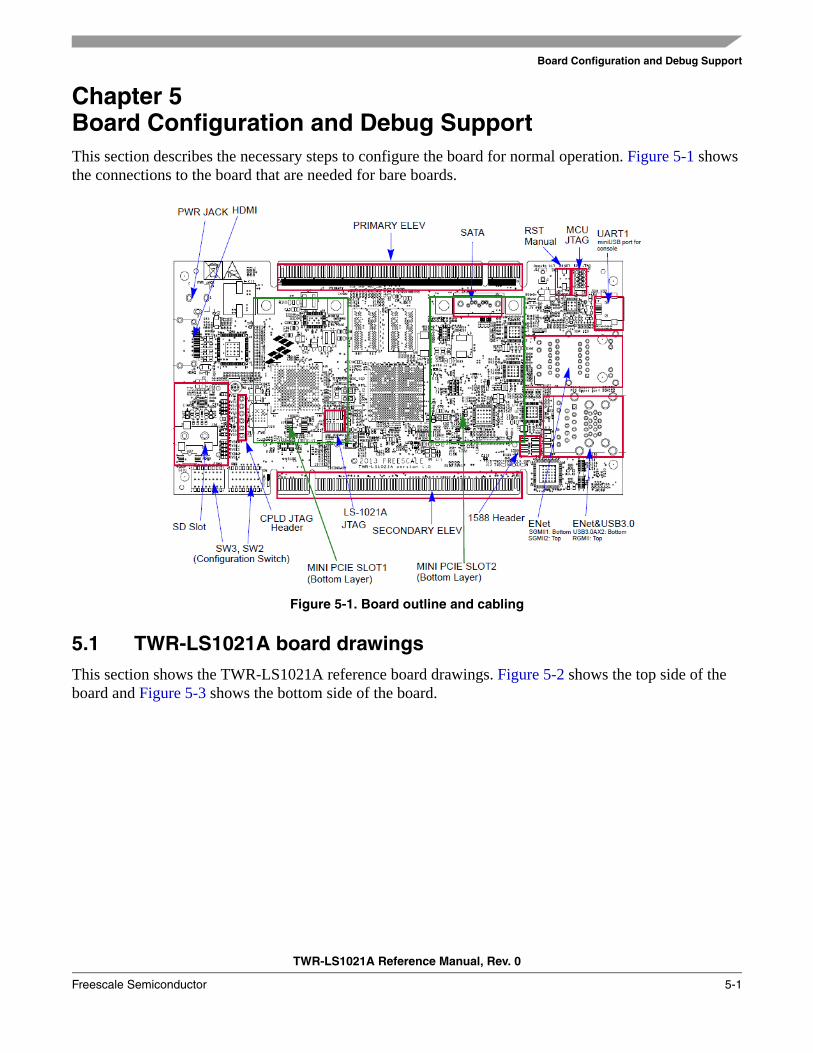
Board Configuration and Debug Support
TWR-LS1021A Reference Manual, Rev. 0
Freescale Semiconductor 5-1
Chapter 5 Board Configuration and Debug SupportThis section describes the necessary steps to configure the board for normal operation. Figure 5-1 shows the connections to the board that are needed for bare boards.
Figure 5-1. Board outline and cabling
5.1 TWR-LS1021A board drawingsThis section shows the TWR-LS1021A reference board drawings. Figure 5-2 shows the top side of the board and Figure 5-3 shows the bottom side of the board.
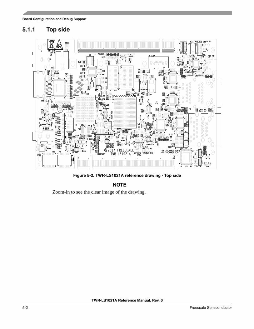
Board Configuration and Debug Support
TWR-LS1021A Reference Manual, Rev. 0
5-2 Freescale Semiconductor
5.1.1 Top side
Figure 5-2. TWR-LS1021A reference drawing - Top side
NOTEZoom-in to see the clear image of the drawing.
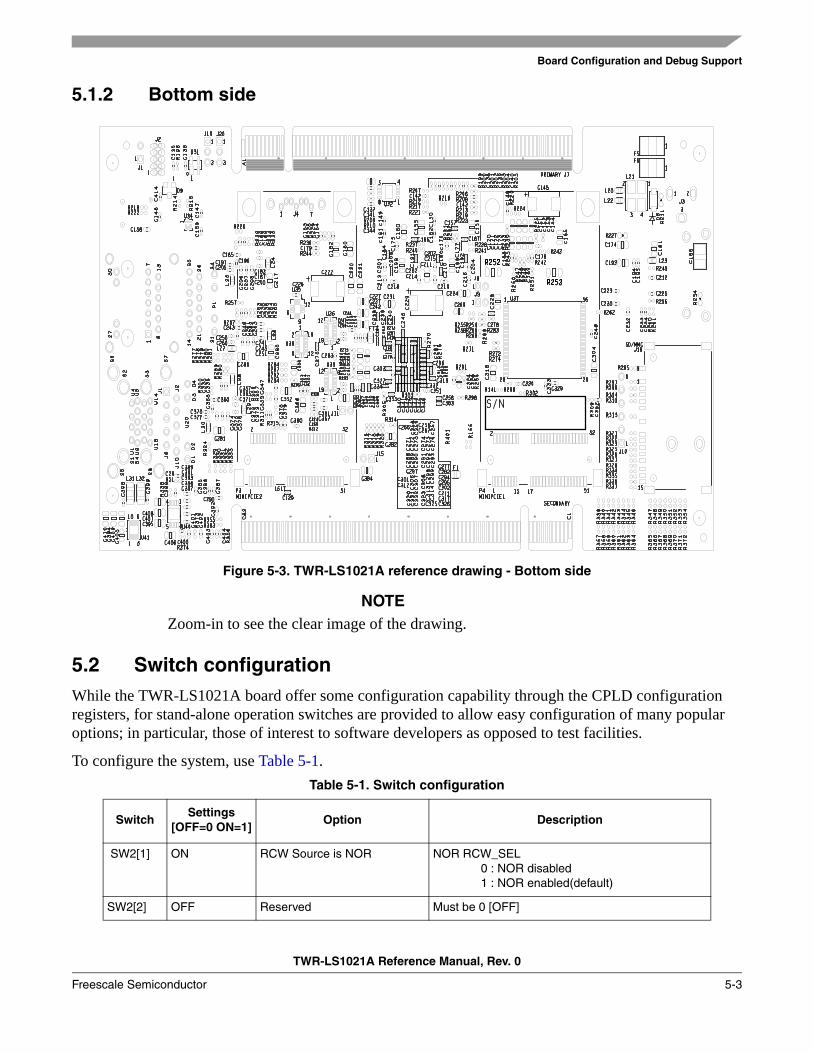
Board Configuration and Debug Support
TWR-LS1021A Reference Manual, Rev. 0
Freescale Semiconductor 5-3
5.1.2 Bottom side
Figure 5-3. TWR-LS1021A reference drawing - Bottom side
NOTEZoom-in to see the clear image of the drawing.
5.2 Switch configurationWhile the TWR-LS1021A board offer some configuration capability through the CPLD configuration registers, for stand-alone operation switches are provided to allow easy configuration of many popular options; in particular, those of interest to software developers as opposed to test facilities.
To configure the system, use Table 5-1.
Table 5-1. Switch configuration
SwitchSettings
[OFF=0 ON=1]Option Description
SW2[1] ON RCW Source is NOR NOR RCW_SEL0 : NOR disabled 1 : NOR enabled(default)
SW2[2] OFF Reserved Must be 0 [OFF]

Board Configuration and Debug Support
TWR-LS1021A Reference Manual, Rev. 0
5-4 Freescale Semiconductor
SW2[3] OFF RCW Source is SDHC SDHC RCW_SEL0 : SDHC disabled (default)1 : SDHC enabled
SW2[4] OFF RCW Source is QSPI QSPI RCW_SEL0 : QSPI disabled (default)1 : QSPI enabled
SW2[5] ON Bus select is NOR or QSPI IFC/QSPI Bus selection0 : IFC disabled, QSPI enabled1 : IFC enabled, QSPI disabled (default)
SW2[6] ON LVDD&L1VDD selection is 2.5V or 3.3V
LVDD&L1VDD Voltage Selection0 : 3.3V 1 : 2.5V (default)
SW2[7] ON IFC_CS1 or SPI1_PCS0 selection
IFC_CS1/SPI1_PCS0 Selection0 : IFC_CS1 disabled, SPI1_PCS0 enabled1 : IFC_CS1 enabled, SPI1_PCS0
disabled (default)
SW2[8] ON DIPSW_IN1 SDA_SWD_EN Control0 : use K20 IO pin to control
SDA_SWD_EN1 : tied to high to disable MBED connection
(default)
SW3[1] OFF 96MHz SYSCLK select or not 96MHz SYSCLK Selection0 : Do not select 96MHz as SYSCLK
(default)1 : Select 96MHz as SYSCLK
SW3[2] ON TEST_SEL_DRV Drive TEST_SEL signal0 : Non-compliant mode to support
boundary scan.1 : JTAG compliant mode (default)
SW3[3] ON CLKGEN_FS0System clock frequency setting
CLKGEN_FS[0:1]00 = 66.66MHz01 = 80.00MHz10 = 100.00MHz (default)11 = 83.33MHz
SW3[4] OFF CLKGEN_FS1System clock frequency setting
SW3[5] OFF NOR Bank SelectBANK_SEL
BANK_SEL0 : Vbank0 (default)1 : Vbank1
SW3[6] OFF Signal multiplexed selectionMUX_SEL
MUX_SEL0 : PCIE1,SGMII1,PCIE2,SGMII2, RGMII, CAN3&4, SAI1&2, LCD, LPUART1 (default)1 : PCIE1,SATA,PCIE2,SGMII2, RGMII, CAN3&4, CAN1&2, UCC1&3, SPI2
SW3[7] OFF Reserved Must be 0 [OFF]
SW3[8] ON Reserved Must be 1 [ON]
SwitchSettings
[OFF=0 ON=1]Option Description
Board Configuration and Debug Support
TWR-LS1021A Reference Manual, Rev. 0
Freescale Semiconductor 5-5
5.3 CMSIS-DAP debug supportThis section describes how to enable CMSIS dap debug support for your TWR-LS1021A board.
NOTEThe TWR-LS1021A 700-28040 board comes pre-programmed with CMSIS-DAP firmware.
To enable the CMSIS-DAP debug support for TWR-LS1021A 700 revX3/X4 board, follow these steps:
1. Download the CMSIS-DAP firmware and documentation from http://compass.freescale.net/livelink/livelink?func=ll&objId=232410365&objAction=browse&viewType=1
2. Plug in power to the TWR-LS1021A 700 revX3/X4 board.
3. Hold down Reset button (SW1) while plugging the PC USB cable into the J5 USB connector on the board.
4. On Windows, the board will be mapped as a Mass Storage Device under a volume labelled BOOTLOADER.
5. LED D2 will blink in green on the board to acknowledge it is in bootloader mode.
6. Copy the binary files downloaded in Step 1, into this new volume, BOOTLOADER.
7. When the binary files are finished copying, the LED D2 will start blinking with a higher rate.
8. Unplug the USB cable from the board, then plug it back to the power cycle module.
9. Set SW2[8] to OFF.
You are now ready to connect to your board through CodeWarrior for ARMv7.
NOTEFor Windows platform, you need to install mbed USB driver. For configuration and installation of Windows serial port, follow the link below:
http://mbed.org/handbook/Windows-serial-configuration

Board Configuration and Debug Support
TWR-LS1021A Reference Manual, Rev. 0
5-6 Freescale Semiconductor


