522
Mitsubishi Programmable Logic Controller Type ACPU/QCPU-A (A Mode)(Common Instructions) Programming Manual

Mitsubishi Programmable Logic Controller
Type ACPU/QCPU-A (A Mode)(Common Instructions)
Programming Manual
MODEL
MODELCODE
ACPU-COMMON-P-E
13J741
IB(NA)-66250-H(0312)MEE
Type ACPU/QCPU-A (A Mode)(Common Instructions)
Programming Manual
P
Type A
CP
U/Q
CP
U-A
(A M
ode)(Com
mon Instructions) P
rogramm
ing Manual
Specifications subject to change without notice.
When exported from Japan, this manual does not require application to theMinistry of Economy, Trade and Industry for service transaction permission.
HEAD OFFICE : 1-8-12, OFFICE TOWER Z 14F HARUMI CHUO-KU 104-6212,JAPANNAGOYA WORKS : 1-14 , YADA-MINAMI 5-CHOME , HIGASHI-KU, NAGOYA , JAPAN

SAFETY CAUTIONS(You must read these cautions before using the product)
In connection with the use of this product, in addition to carefully reading both this manual and the relatedmanuals indicated in this manual, it is also essential to pay due attention to safety and handle the productcorrectly.The safety cautions given here apply to this product in isolation. For information on the safety of the PCsystem as a whole, refer to the CPU module User's Manual.Store this manual carefully in a place where it is accessible for reference whenever necessary, and forward acopy of the manual to the end user.
A − 1
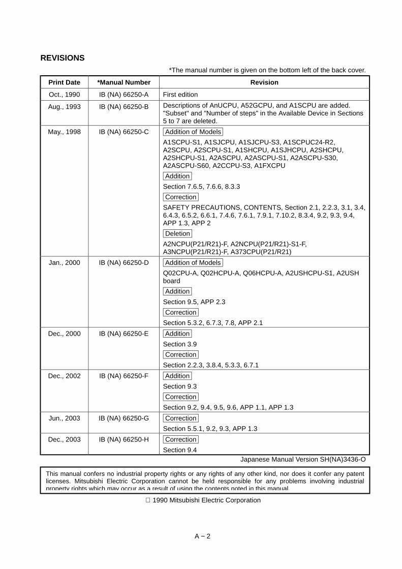
REVISIONS*The manual number is given on the bottom left of the back cover.
Print Date *Manual Number Revision
Oct., 1990 IB (NA) 66250-A First edition
Aug., 1993 IB (NA) 66250-B Descriptions of AnUCPU, A52GCPU, and A1SCPU are added."Subset" and "Number of steps" in the Available Device in Sections5 to 7 are deleted.
May., 1998 IB (NA) 66250-C Addition of Models A1SCPU-S1, A1SJCPU, A1SJCPU-S3, A1SCPUC24-R2,A2SCPU, A2SCPU-S1, A1SHCPU, A1SJHCPU, A2SHCPU,A2SHCPU-S1, A2ASCPU, A2ASCPU-S1, A2ASCPU-S30,A2ASCPU-S60, A2CCPU-S3, A1FXCPU Addition Section 7.6.5, 7.6.6, 8.3.3 Correction SAFETY PRECAUTIONS, CONTENTS, Section 2.1, 2.2.3, 3.1, 3.4,6.4.3, 6.5.2, 6.6.1, 7.4.6, 7.6.1, 7.9.1, 7.10.2, 8.3.4, 9.2, 9.3, 9.4,APP 1.3, APP 2 Deletion A2NCPU(P21/R21)-F, A2NCPU(P21/R21)-S1-F,A3NCPU(P21/R21)-F, A373CPU(P21/R21)
Jan., 2000 IB (NA) 66250-D Addition of Models Q02CPU-A, Q02HCPU-A, Q06HCPU-A, A2USHCPU-S1, A2USHboard Addition Section 9.5, APP 2.3 Correction Section 5.3.2, 6.7.3, 7.8, APP 2.1
Dec., 2000 IB (NA) 66250-E Addition Section 3.9 Correction Section 2.2.3, 3.8.4, 5.3.3, 6.7.1
Dec., 2002 IB (NA) 66250-F Addition Section 9.3 Correction Section 9.2, 9.4, 9.5, 9.6, APP 1.1, APP 1.3
Jun., 2003 IB (NA) 66250-G Correction Section 5.5.1, 9.2, 9.3, APP 1.3
Dec., 2003 IB (NA) 66250-H Correction Section 9.4
Japanese Manual Version SH(NA)3436-O
1990 Mitsubishi Electric Corporation
A − 2
This manual confers no industrial property rights or any rights of any other kind, nor does it confer any patentlicenses. Mitsubishi Electric Corporation cannot be held responsible for any problems involving industrialproperty rights which may occur as a result of using the contents noted in this manual.

INTRODUCTION
Thank you for choosing the Mitsubishi MELSEC-A Series of General Purpose Programmable Controllers.Please read this manual carefully so that the equipment is used to its optimum. A copy of this manual shouldbe forwarded to the end User.
A − 3

A − 4
CONTENTS
1. INTRODUCTION ......................................................................................................................1 −−−− 1 ~ 1 −−−− 3
2. INSTRUCTIONS.....................................................................................................................2 −−−− 1 ~ 2 −−−− 24
2.1 Classification...............................................................................................................................2 − 1
2.2 Instruction List.............................................................................................................................2 − 22.2.1 Explanation for instructions lists ....................................................................................2 − 22.2.2 Sequence instructions ...................................................................................................2 − 52.2.3 Basic instructions...........................................................................................................2 − 82.2.4 Application instructions ................................................................................................2 − 16
3. INSTRUCTION STRUCTURE ................................................................................................3 −−−− 1 ~ 3 −−−− 24
3.1 Instruction Structure....................................................................................................................3 − 1
3.2 Bit Processing .............................................................................................................................3 − 33.2.1 1-bit processing..............................................................................................................3 − 33.2.2 Digit specification processing ........................................................................................3 − 3
3.3 Handling of Numeric Values .......................................................................................................3 − 6
3.4 Storing 32-bit Data......................................................................................................................3 − 8
3.5 Index Qualification ....................................................................................................................3 − 103.6 Subset Processing....................................................................................................................3 − 12
3.7 Operation Error .........................................................................................................................3 − 12
3.8 Cautions on Using AnA, A2AS, AnU, QCPU-A (A Mode) and A2USH board..........................3 − 143.8.1 The number of steps used in instructions....................................................................3 − 143.8.2 Instructions of variable functions .................................................................................3 − 163.8.3 Set values for the extension timer and counter ...........................................................3 − 173.8.4 Cautions on using index qualification ..........................................................................3 − 173.8.5 Storing 32-bit data in index registers ...........................................................................3 − 20
3.9 Operation when the OUT Instruction, SET/RST Instruction andPLS/PLF Instruction are from the Same Device .........................................................................3 − 21
4. INSTRUCTION FORMAT .........................................................................................................4 −−−− 1 ~ 4 −−−− 3
5. SEQUENCE INSTRUCTIONS................................................................................................5 −−−− 4 ~ 5 −−−− 41
5.1 Contact Instructions ....................................................................................................................5 − 25.1.1 Operation start, series connection,parallel connection
(LD, LDI, AND, ANI, OR, ORI).......................................................................................5 − 25.2 Connection Instructions ..............................................................................................................5 − 5
5.2.1 Ladder block series connection, parallel connection (ANB, ORB) ................................5 − 55.2.2 Operation result push, read, pop (MPS, MRD, MPP)....................................................5 − 9
5.3 Output Instructions....................................................................................................................5 − 145.3.1 Bit device, timer, counter output (OUT) .......................................................................5 − 145.3.2 Bit device set, reset (SET,RST) ...................................................................................5 − 195.3.3 Edge-triggered differential output (PLS, PLF) .............................................................5 − 235.3.4 Bit device output reverse (CHK) ..................................................................................5 − 25

A − 5
5.4 Shift Instructions .......................................................................................................................5 − 275.4.1 Bit device shift (SFT, SFTP).........................................................................................5 − 27
5.5 Master Control Instructions.......................................................................................................5 − 295.5.1 Master control set, reset (MC, MCR)...........................................................................5 − 29
5.6 Termination Instructions............................................................................................................5 − 335.6.1 Main routine program termination (FEND) ..................................................................5 − 335.6.2 Sequence program termination (END) ........................................................................5 − 35
5.7 Other Instructions......................................................................................................................5 − 375.7.1 Sequence program stop (STOP) .................................................................................5 − 375.7.2 No operation (NOP, NOPLF) .......................................................................................5 − 39
6. BASIC INSTRUCTIONS.........................................................................................................6 −−−− 1 ~ 6 −−−− 89
6.1 Comparison Operation Instructions ............................................................................................6 − 26.1.1 16-bit data comparison (=, <>, >, <=, <, >=)..................................................................6 − 46.1.2 32-bit data comparison (D=, D<>, D>, D<=, D<,D>=) ...................................................6 − 6
6.2 Arithmetic Operation Instructions................................................................................................6 − 86.2.1 BIN 16-bit addition, subtraction (+, +P, -, -P) ...............................................................6 − 106.2.2 BIN 32-bit addition, subtraction (D+, D+P, D-, D-P).....................................................6 − 136.2.3 BIN 16-bit multiplication, division (*, *P, /, /P) ..............................................................6 − 166.2.4 BIN 32-bit multiplication, division (D*, D*P, D/, D/P)....................................................6 − 196.2.5 BCD 4-digit addition, subtraction (B+, B+P, B-, B-P) ...................................................6 − 226.2.6 BCD 8-digit addition, subtraction (DB+, DB+P, DB-, DB-P).........................................6 − 256.2.7 BCD 4-digit multiplication, division (B*, B*P, B/, B/P) ..................................................6 − 286.2.8 BCD 8-digit multiplication, division (DB*, DB*P, DB/, DB/P)........................................6 − 316.2.9 16-bit BIN data increment, decrement (INC, INCP, DEC, DECP) ...............................6 − 346.2.10 32-bit BIN data increment, decrement (DINC, DINCP, DDEC, DDECP).....................6 − 36
6.3 BCD ↔ BIN Conversion Instructions........................................................................................6 − 386.3.1 BIN data → BCD 4-, 8-digit conversion (BCD, BCDP, DBCD, DBCDP) .....................6 − 396.3.2 BCD 4-, 8-digit → BIN data conversion (BIN, BINP, DBIN, DBINP)............................6 − 42
6.4 Data Transfer Instructions.........................................................................................................6 − 466.4.1 16-, 32-bit data transfer (MOV, MOVP, DMOV, DMOVP) ............................................6 − 476.4.2 16-, 32-bit data negation transfer (CML, CMLP, DCML, DCMLP)...............................6 − 496.4.3 16-bit data block transfer (BMOV, BMOVP, FMOV, FMOVP)......................................6 − 526.4.4 16-, 32-bit data exchange (XCH, XCHP, DXCH, DXCHP) ..........................................6 − 56
6.5 Program Branch Instructions ....................................................................................................6 − 586.5.1 Conditional jump, unconditional jump (CJ, SCJ, JMP)................................................6 − 586.5.2 Subroutine call, return (CALL, CALLP, RET)...............................................................6 − 626.5.3 Interrupt enable, disable, return (EI, DI, IRET) ............................................................6 − 646.5.4 Microcomputer program call (SUB, SUBP) .................................................................6 − 67
6.6 Program Switching Instructions ................................................................................................6 − 696.6.1 Main ↔ subprogram switching (CHG).........................................................................6 − 69

A − 6
6.7 Link Refresh Instructions ..........................................................................................................6 − 826.7.1 Link refresh (COM) ......................................................................................................6 − 826.7.2 Link refresh enable, disable (EI, DI) ............................................................................6 − 846.7.3 Partial refresh (SEG) ...................................................................................................6 − 87
7. APPLICATION INSTRUCTIONS..........................................................................................7 −−−− 1 ~ 7 −−−− 133
7.1 Logical Operation Instructions ....................................................................................................7 − 27.1.1 16-, 32-bit data logical product (WAND, WANDP, DAND, DANDP) ..............................7 − 37.1.2 16-, 32-bit data logical add (WOR, WORP, DOR, DORP).............................................7 − 77.1.3 16-, 32-bit data exclusive logical add (WXOR, WXORP, DXOR, DXORP) ................. 7 − 117.1.4 16, 32-bit data NOT exclusive logical add (WXNR, WXNRP, DXNR, DXNRP)...........7 − 157.1.5 BIN 16-bit data 2’s complement (NEG, NEGP) ...........................................................7 − 19
7.2 Rotation Instructions .................................................................................................................7 − 217.2.1 16-bit data right rotation (ROR, RORP, RCR, PCRP) .................................................7 − 227.2.2 16-bit data left rotation (ROL, ROLR, RCL, RCLP) .....................................................7 − 247.2.3 32-bit data right rotation (DROR, DRORP, DRCR, DRCRP).......................................7 − 267.2.4 32-bit data left rotation (DROL, DROLP, DRCL, DRCLP) ...........................................7 − 28
7.3 Shift Instructions .......................................................................................................................7 − 307.3.1 16-bit data n-bit right shift, left shift (SFR, SFRP, SFL, SFLP) ....................................7 − 317.3.2 n-bit data 1-bit right shift, left shift (BSFR, BSFRP, BSFL, BSFLP) ............................7 − 337.3.3 n-word data 1-word right shift, left shift (DSFR, DSFRP, DSFL, DSFLP)....................7 − 35
7.4 Data Processing Instructions ....................................................................................................7 − 377.4.1 16-bit data search (SER, SERP) .................................................................................7 − 387.4.2 16-, 32-bit data bit check (SUM, SUMP, DSUM, DSUMP) ..........................................7 − 407.4.3 8 ↔ 256-bit decode, encode (DECO, DECOP, ENCO, ENCOP)................................7 − 427.4.4 7 segment decode (SEG) ............................................................................................7 − 447.4.5 Word device bit set, reset (BSET, BSETP, BRST, BRSTP) .........................................7 − 467.4.6 16-bit data dissociation, association (DIS, DISP, UNI, UNIP) .....................................7 − 487.4.7 ASCII code conversion (ASC) .....................................................................................7 − 51
7.5 FIFO Instructions ......................................................................................................................7 − 537.5.1 FIFO table write, read (FIFW, FIFWP, FIFR, FIFRP)...................................................7 − 54
7.6 Buffer Memory Access Instructions ..........................................................................................7 − 587.6.1 Special function module 1-, 2-word data read (FROM, FROMP, DFRO, DFROP) .....7 − 597.6.2 Special function module 1-, 2-word data write (TO, TOP, DTO, DTOP)......................7 − 617.6.3 Remote terminal module 1- and 2-word data read
(FROM, PRC, FROMP, PRC, DFRO, PRC, DFROP, PRC) ........................................7 − 637.6.4 Remote terminal module 1- and 2-word data write
(TO, PRC, TOP, PRC, DTO, PRC, DTOP, PRC) .........................................................7 − 677.6.5 Special module/special block 1-, 2-word data read
(FROM, FROMP, DFRO, DFROP) ..............................................................................7 − 717.6.6 Special module/special block 1-, 2-word data write (TO, TOP, DTO, DTOP)..............7 − 74
7.7 FOR to NEXT Instructions ........................................................................................................7 − 777.7.1 FOR to NEXT (FOR, NEXT)........................................................................................7 − 77
A − 7
7.8 Local, Remote I/O Station Access Instructions ........................................................................7 − 797.8.1 Local station data read, write (LRDP, LWTP) ..............................................................7 − 807.8.2 Remote I/O station data read, Write (RFRP, RTOP) ...................................................7 − 86
7.9 Display Instructions...................................................................................................................7 − 927.9.1 ASCII code print instructions (PR, PRC) .....................................................................7 − 947.9.2 ASCII code comment display instructions (LED, LEDC) ...........................................7 − 1007.9.3 Character display instructions (LEDA, LEDB) ...........................................................7 − 1037.9.4 Annunciator reset instruction (LEDR) ........................................................................7 − 105
7.10 Other Instructions....................................................................................................................7 − 1087.10.1 WDT reset (WDT, WDTP)..........................................................................................7 − 1097.10.2 Specific format failure check (CHK)........................................................................... 7 − 1117.10.3 Status latch set, reset (SLT, SLTR)............................................................................ 7 − 1177.10.4 Sampling trace set, reset (STRA, STRAR)................................................................ 7 − 1197.10.5 Carry flag set, reset (STC, CLC)................................................................................7 − 1217.10.6 Pulse regeneration instruction (DUTY)......................................................................7 − 123
7.11 Servo Program Instructions ....................................................................................................7 − 1257.11.1 Servo program start (DSFRP) ...................................................................................7 − 1267.11.2 Present position data and speed change instruction (DSFLP)..................................7 − 130
8. MICROCOMPUTER MODE ...................................................................................................8 −−−− 1 ~ 8 −−−− 16
8.1 Specifications of Microcomputer Mode.......................................................................................8 − 1
8.2 Using Utility Program ..................................................................................................................8 − 2
8.3 Using User-Written Microcomputer Programs............................................................................8 − 48.3.1 Memory map..................................................................................................................8 − 68.3.2 Data memory area address configuration .....................................................................8 − 68.3.3 Differences in operations called by microcomputer instructions
according to CPU models ..............................................................................................8 − 78.3.4 Configuration of data memory area ...............................................................................8 − 8
9. ERROR CODE LIST...............................................................................................................9 −−−− 1 ~ 9 −−−− 41
9.1 Reading Error Codes ..................................................................................................................9 − 1
9.2 Error Code List for the An, AnN, A3H, A3M, A3V, A0J2H, AnS, A2C, A73, A52G, A1FX and A3Nboard...........................................................................................................................................9 − 1
9.3 Error Code List for AnSHCPU ....................................................................................................9 − 7
9.4 Error Code List for the AnACPU...............................................................................................9 − 13
9.5 Error Code List for the AnUCPU, A2ASCPU and A2USH board .............................................9 − 229.6 Error Code List for the QCPU-A (A Mode) ...............................................................................9 − 33
APPENDICES .....................................................................................................................APP −−−− 1 ~ APP −−−− 96
APPENDIX 1 LISTS OF SPECIAL RELAYS AND SPECIAL REGISTERS ...................................APP − 1
1.1 List of Special Relays ............................................................................................................APP − 11.2 Special Relays for Link ........................................................................................................APP − 13
1.3 Special Registers .................................................................................................................APP − 16
1.4 Special Registers for Link ....................................................................................................APP − 34

A − 8
APPENDIX 2 OPERATION PROCESSING TIME........................................................................APP − 392.1 Instruction Processing Time of Small Size, Compact CPUs ...............................................APP − 412.2 Instruction Processing Time of CPUs ..................................................................................APP − 66
2.3 Instruction Processing Time of QCPU-A (A Mode)..............................................................APP − 79
APPENDIX 3 ASCII CODE TABLE...............................................................................................APP − 89APPENDIX 4 FORMATS OF PROGRAM SHEETS .....................................................................APP − 90

1. INTRODUCTION
1 − 1
MELSEC-A
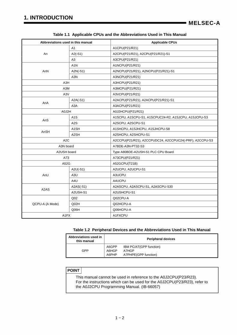
1. INTRODUCTION
This manual explains how to use the MELSEC-A series sequence controlinstructions and microcomputer programs.MELSEC-A series programmable controllers have a parameter which is used todesignate functions and device use ranges.The functions and device use ranges are determined by the parameter values.The parameters of CPU are set to default values. If the default can be used for thepurpose, it is not necessary to set the parameter.The user’s programs for the MELSEC-A series PCs are classified as follows.ACPU Programming Manual (fundamental) gives the programs which can be usedfor CPUs.
Table 1.1 gives the applicable CPUs the abbreviations used in this manual.
User’sprogram
Main routine program
Subroutine program
Interruption program
Utility program
User creatingmicrocomputer program
Main routine program
Subroutine program
Interruption program
User creatingmicrocomputer program
Subsequenceprogram
Submicrocomputerprogram
Sequence program
Microcomputerprogram
Main program
Subprogram
1. INTRODUCTION
1 − 2
MELSEC-A
Table 1.1 Applicable CPUs and the Abbreviations Used in This Manual
Abbreviations used in this manual Applicable CPUsA1 A1CPU(P21/R21)
A2(-S1) A2CPU(P21/R21), A2CPU(P21/R21)-S1An
A3 A3CPU(P21/R21)
A1N A1NCPU(P21/R21)
A2N(-S1) A2NCPU(P21/R21), A2NCPU(P21/R21)-S1AnN
A3N A3NCPU(P21/R21)
A3H A3HCPU(P21/R21)
A3M A3MCPU(P21/R21)
A3V A3VCPU(P21/R21)
A2A(-S1) A2ACPU(P21/R21), A2ACPU(P21/R21)-S1AnA
A3A A3ACPU(P21/R21)
A0J2H A0J2HCPU(P21/R21)
A1S A1SCPU, A1SCPU-S1, A1SCPUC24-R2, A1SJCPU, A1SJCPU-S3AnS
A2S A2SCPU, A2SCPU-S1
A1SH A1SHCPU, A1SJHCPU, A1SJHCPU-S8AnSH
A2SH A2SHCPU, A2SHCPU-S1
A2C A2CCPU(P21/R21), A2CCPUDC24, A2CCPUC24(-PRF), A2CCPU-S3
A3N board A7BDE-A3N-PT32-S3
A2USH board Type A80BDE-A2USH-S1 PLC CPU Board
A73 A73CPU(P21/R21)
A52G A52GCPU(T21B)
A2U(-S1) A2UCPU, A2UCPU-S1
A3U A3UCPUAnU
A4U A4UCPU
A2AS(-S1) A2ASCPU, A2ASCPU-S1, A2ASCPU-S30A2AS
A2USH-S1 A2USHCPU-S1
Q02 Q02CPU-A
Q02H Q02HCPU-AQCPU-A (A Mode)
Q06H Q06HCPU-A
A1FX A1FXCPU
Abbreviations used inthis manual Peripheral devices
GPPA6GPP IBM PC/AT(GPP function)A6HGP A7HGPA6PHP A7PHPE(GPP function)
POINTThis manual cannot be used in reference to the A0J2CPU(P23/R23).For the instructions which can be used for the A0J2CPU(P23/R23), refer tothe A0J2CPU Programming Manual. (IB-66057)
Table 1.2 Peripheral Devices and the Abbreviations Used in This Manual
1. INTRODUCTION
1 − 3
MELSEC-A
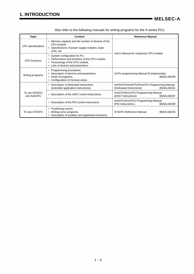
Also refer to the following manuals for writing programs for the A series PCs.
Topic Content Reference Manual
CPU specifications
• Memory capacity and the number of devices of theCPU module.
• Specifications of power supply modules, baseunits, etc.
CPU functions
• System configuration for PC.• Performance and functions of the CPU module.• Processings of the CPU module.• Lists of devices and parameters.
User’s Manual for respective CPU module
Writing programs
• Programming procedures.• Description of devices and parameters.• Kinds of programs.• Configuration of memory areas.
ACPU programming Manual (Fundamentals)IB(NA)-66249
• Description of dedicated instructions(extended application instructions).
AnSHCPU/AnACPU/AnUCPU Programming Manual(Dedicated Instructions) IB(NA)-66251
• Description of the AD57 control instructions. AnACPU/AnUCPU Programming Manual(AD57 Instructions) IB(NA)-66257
To use A2A(S1)and A3ACPU
• Description of the PID control instructions. AnACPU/AnUCPU Programming Manual(PID Instructions.) IB(NA)-66258
To Use A73CPU• Positioning control.• Writing servo programs.• Description of auxiliary and application functions.
A73CPU Reference Manual IB(NA)-66233

2. INSTRUCTIONS
2 − 1
MELSEC-A
2. INSTRUCTIONS
2.1 Classification
The instructions of MELSEC-A series are largely classified into sequence instruc-tions, basic instructions, and application instructions. These instructions are shownin Table 2.1.
Table 2.1 Classification of Instructions
Classification of instructions Description page
Contact instruction Operation start, series connection, parallelconnection 5-2 to 5-4
Connection instruction Ladder block connection, operation resultstorage/read 5-5 to 5-13
Output instruction Bit device output, pulse output, output reverse 5-14 to 5-26
Shift instruction Bit device shift 5-27 to 5-28
Master control instruction Master control 5-29 to 5-32
Termination instruction Program termination 5-33 to 5-36
Sequenceinstruction
Other instructions Program stop, no operation, etc. 5-37 to 5-42
Comparison operation instruction Comparison such as =, >, and < 6-2 to 6-7
Arithmetic operation instruction Addition, subtraction, multiplication, anddivision of BIN and BCD 6-8 to 6-37
BCD ↔ BIN conversion instruction Conversion from BCD to BIN and BIN to BCD 6-38 to 6-45
Data transfer instruction Transfer of specified data 6-46 to 6-57
Program branch instruction Program jump, subroutine/interrupt program call 6-58 to 6-68
Program switching instruction Switching between main and subprogram 6-69 to 6-81
Basicinstruction
Refresh instruction Link refresh, partial refresh execution 6-82 to 6-88
Logical operation instruction Logical operation such as logical sum and logicalproduct 7-2 to 7-20
Rotation instruction Rotation of specified data 7-21 to 7-29
Shift instruction Shift of specified data 7-30 to 7-36
Data processing instruction Data processing such as 16-bit data search,decode, and encode 7-37 to 7-52
FIFO instruction Read/write of FIFO table 7-53 to 7-57
Buffer memory access instruction Data read/write with special function modules andremote terminals(A2C/A52G). 7-58 to 7-76
FOR to NEXT instruction Program repeated between FOR and NEXTinstruction 7-77 to 7-78
Local, remote I/O station accessinstruction Local, remote I/O station data read/write 7-79 to 7-91
Display instruction ASCll code print, character display on LED, etc. 7-92 to 7-107
OthersInstructions which are not included in the above
classification, such as WDT reset, and set/reset ofcarry flag.
7-108 to 7-124
Applicationinstruction
Instructions for servo programs Servo program execution and set value change 7-125 to 7-133
2. INSTRUCTIONS
2 − 2
MELSEC-A
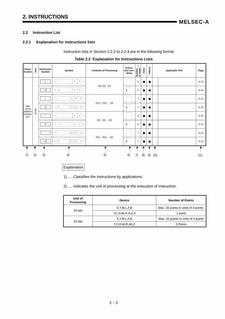
2.2 Instruction List
2.2.1 Explanation for instructions lists
Instruction lists in Section 2.2.2 to 2.2.4 are in the following format.
Table 2.2 Explanation for Instructions Lists
Classi-fication U
nit Instruction
Symbol Symbol Contents of ProcessingExecu-
tion Con-dition
Num
ber
of s
teps
Inde
x
Subs
et
Applicable CPU Page
+ 5 ● ●� 6-10
+P
(D)+(S)→(D)
5 ● ●� 6-10
+ 7 ● ●� 6-10
+P
(S1) + (S2) → (D)
7 ● ●� 6-10
- 5 ● ●� 6-10
-P
(D) - (S) → (D)
5 ● ●� 6-10
- 7 ● ●� 6-10
BIN16-bit
addition/subtrac
tion
16 b
its
+P
(S1) - (S2) → (D)
7 ● ●� 6-10
Explanation
1)….. Classifies the instructions by applications.
2)….. Indicates the unit of processing at the execution of instruction.
Unit ofProcessing Device Number of Points
X,Y,M,L,F,B Max. 16 points in units of 4 points.16 bits
T,C,D,W,R,A,Z,V 1 point
X,Y,M,L,F,B Max. 32 points In units of 4 points32 bits
T,C,D,W,R,A0,Z 2 Points
+P DS1 S2
*1
1) 2) 3) 4) 5) 6) 7) 8) 9) 10) 11)
+ DS
+P DS
+ DS1 S2
+P DS1 S2
- DS
- DS1 S2
- P S D
2. INSTRUCTIONS
2 − 3
MELSEC-A
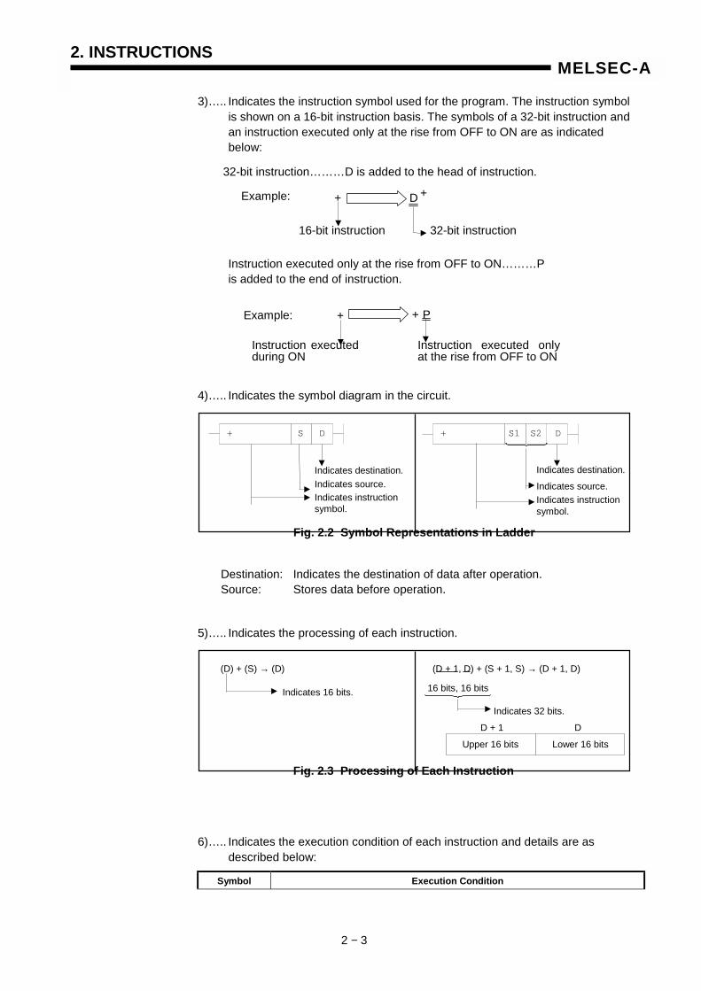
3)….. Indicates the instruction symbol used for the program. The instruction symbol is shown on a 16-bit instruction basis. The symbols of a 32-bit instruction and an instruction executed only at the rise from OFF to ON are as indicated below:
Instruction executed only at the rise from OFF to ON………Pis added to the end of instruction.
4)….. Indicates the symbol diagram in the circuit.
Destination: Indicates the destination of data after operation.Source: Stores data before operation.
5)….. Indicates the processing of each instruction.
6)….. Indicates the execution condition of each instruction and details are as described below:
Symbol Execution Condition
32-bit instruction………D is added to the head of instruction.
+ D +Example:
16-bit instruction 32-bit instruction
Example: + P+
Instruction executedduring ON
Instruction executed onlyat the rise from OFF to ON
+ DS
Indicates destination.Indicates source.Indicates instructionsymbol.
Indicates destination.
Indicates source.Indicates instructionsymbol.
+ DS1 S2
Fig. 2.2 Symbol Representations in Ladder
(D) + (S) → (D)
Indicates 16 bits.
(D + 1, D) + (S + 1, S) → (D + 1, D)
16 bits, 16 bits
Indicates 32 bits.
Upper 16 bits Lower 16 bits
D + 1 D
Fig. 2.3 Processing of Each Instruction
2. INSTRUCTIONS
2 − 4
MELSEC-A
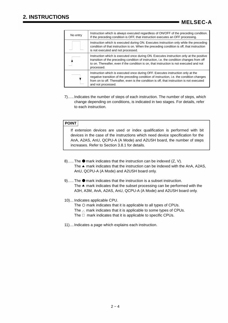
No entry Instruction which is always executed regardless of ON/OFF of the preceding condition.If the preceding condition is OFF, that instruction executes an OFF processing.
Instruction which is executed during ON. Executes instruction only while the precedingcondition of that instruction is on. When the preceding condition is off, that instructionis not executed and not processed.
Instruction which is executed once during ON. Executes instruction only at the positivetransition of the preceding condition of instruction, i.e. the condition changes from offto on. Thereafter, even if the condition is on, that instruction is not executed and notprocessed.
Instruction which is executed once during OFF. Executes instruction only at thenegative transition of the preceding condition of instruction, i.e. the condition changesfrom on to off. Thereafter, even is the condition is off, that instruction is not executedand not processed.
7)….. Indicates the number of steps of each instruction. The number of steps, which change depending on conditions, is indicated in two stages. For details, refer to each instruction.
POINT
If extension devices are used or index qualification is performed with bitdevices in the case of the instructions which need device specification for theAnA, A2AS, AnU, QCPU-A (A Mode) and A2USH board, the number of stepsincreases. Refer to Section 3.8.1 for details.
8)….. The ● mark indicates that the instruction can be indexed (Z, V).The mark indicates that the instruction can be indexed with the AnA, A2AS, AnU, QCPU-A (A Mode) and A2USH board only.
9)….. The ● mark indicates that the instruction is a subset instruction.The mark indicates that the subset processing can be performed with the A3H, A3M, AnA, A2AS, AnU, QCPU-A (A Mode) and A2USH board only.
10)… Indicates applicable CPU.The ! mark indicates that it is applicable to all types of CPUs.The mark indicates that it is applicable to some types of CPUs.The mark indicates that it is applicable to specific CPUs.
11).... Indicates a page which explains each instruction.

2. INSTRUCTIONS
2 − 5
MELSEC-A
2.2.2 Sequence instructions
(1) Contact instructionsTable 2.3 Contact Instructions
Classi-fication U
nit Instruction
Symbol Symbol Contents of ProcessingExecu-
tion Con-dition
Num
ber
of s
teps
Inde
x
Subs
et
Applicable CPU Page
LD Logical operation start(NO contact operation start) 1 ! 5-2
LDI Logical NOT operation start(NC contact operation start) 1 ! 5-2
AND Logical product(NO contact series connection) 1 ! 5-2
ANI Logical product NOT(NC contact series connection) 1 ! 5-2
OR Logical add(NO contact parallel connection) 1 ! 5-2
Contact
ORI Logical add NOT(NC contact parallel connection) 1 ! 5-2
(2) Connection instructions
Table 2.4 Connection Instructions
Classi-fIcation U
nit Instruction
Symbol Symbol Contents of ProcessingExecu-
tion Con-dition
Num
ber
of s
teps
Inde
x
Subs
et
Applicable CPU Page
ANB ANDs logical blocks. (Series connection of blocks) 1 ! 5-5
ORB Ors logical blocks.(Parallel connection of blocks) 1 ! 5-5
MPS Stores the operation result. 1 ! 5-9
MRD Reads the operation resultfrom MPS 1 ! 5-9
Connec-tion
MPP Reads the operation result fromMPS and clears the result. 1 ! 5-9
*1: For the number of steps when extension devices are used or when index qualification is performedto bit devices for AnA, A2AS, AnU, QCPU-A (A Mode) and A2USH board, refer to Section 3.8.1.
*2: The mark in the Index column indicates that index qualification can be performed with the AnA,A2AS, AnU, QCPU-A (A Mode) and A2USH board only.
*3: The mark in the Subset column indicates that subset processing can be performed with the A3H,A3M, AnA, A2AS, AnU, QCPU-A (A Mode) and A2USH board only.
MPS
MRD
MPP
*2
*2
*2
*2
*2
*2
*1
*1

2. INSTRUCTIONS
2 − 6
MELSEC-A
(3) Output instructionsTable 2.5 Output instructions
Classi-fication U
nit Instruction
Symbol Symbol Contents of ProcessingExecu-
tion Con-dition
Num
ber
of s
teps
Inde
x
Subs
et
Applicable CPU Page
1OUT Device output
3 ! 5-14
1SET Device set *
3 ! 5-19
1RST Device reset *
3 ! 5-19
PLSGenerates one-program cycle
pulses on the leading edge of inputsignal.
3 ! 5-23
PLFGenerates one-program cycle
pulses on the trailing edge of inputsignal.
3 ! 5-23
OUT
CHK Device output reverse Valid in I/Orefresh mode 5
Not applicable to An, A3V, A2C,A3H, A3M, A52G, AnA, A2AS,QCPU-A (A Mode) and AnU.
5-25
REMARK
Execution Condition marked * in (3) Output instructions:When the device used is F (annunciator).
When the other device is used.
(4) Shift instructionsTable 2.6 Shift Instructions
Classi-fication U
nit Instruction
Symbol Symbol Contents of ProcessingExecu-
tion Con-dition
Num
ber
of s
teps
Inde
x
Subs
et
Applicable CPU Page
SFT 3 ! 5-27Shift
SFTPShifts device 1 bit
3 ! 5-27
(5) Master control instructions
Table 2.7 Master Control Instructions
Classi-fication U
nit Instruction
Symbol Symbol Contents of ProcessingExecu-
tion Con-dition
Num
ber
of s
teps
Inde
x
Subs
et
Applicable CPU Page
MC Master control start 5 ! 5-29Mastercontrol
MCR Master control reset 3 ! 5-29
*1: For the number of steps when extension devices are used or when index qualification is performedto bit devices for AnA, A2AS, AnU, QCPU-A (A Mode) and A2USH board, refer to Section 3.8.1.
*2: The mark in the Index column indicates that index qualification can be performed with the AnA,A2AS, AnU, QCPU-A (A Mode) and A2USH board only.
*3: The mark in the Subset column indicates that subset processing can be performed with the A3H,A3M, AnA, A2AS, AnU, QCPU-A (A Mode) and A2USH board only.
SET D
*2
*2
*2
*2
*2
*2
*2
RST D
PLS D
PLF D
CHK D1 D2
*1
*1
*2
SFT D
SFTP D
*1
MC n D
MCR n

2. INSTRUCTIONS
2 − 7
MELSEC-A
(6) Termination instructionsTable 2.8 Termination Instructions
Classi-fication U
nit Instruction
Symbol Symbol Contents of ProcessingExecu-
tion Con-dition
Num
ber
of s
teps
Inde
x
Subs
et
Applicable CPU Page
FENDAlways used at the end of the main
routine program toterminate processing.
1 ! 5-33Program
end END
Always used at the end of thesequence program to return to
step 0.1 ! 5-35
(7) Other instructionsTable 2.9 Other Instructions
Classi-fication U
nit Instruction
Symbol Symbol Contents of ProcessingExecu-
tion Con-dition
Num
ber
of s
teps
Inde
x
Subs
et
Applicable CPU Page
Stop STOP
Resets output after the inputcondition is enabled, and stops thesequence program. The sequenceprogram is resumed by setting the
RUN key switch to RUN.
1!
5-37
Noopera-
tion NOP No operation
For program erasure or space 1!
5-39
*1: For the number of steps when extension devices are used or when index qualification is performedto bit devices for AnA, A2AS, AnU, QCPU-A (A Mode) and A2USH board, refer to Section 3.8.1.
*2: The mark in the Index column indicates that index qualification can be performed with the AnA,A2AS, AnU, QCPU-A (A Mode) and A2USH board only.
*3: The mark in the Subset column indicates that subset processing can be performed with the A3H,A3M, AnA, A2AS, AnU, QCPU-A (A Mode) and A2USH board only.
STOP
*1
*1
FEND
2. INSTRUCTIONS
2 − 8
MELSEC-A
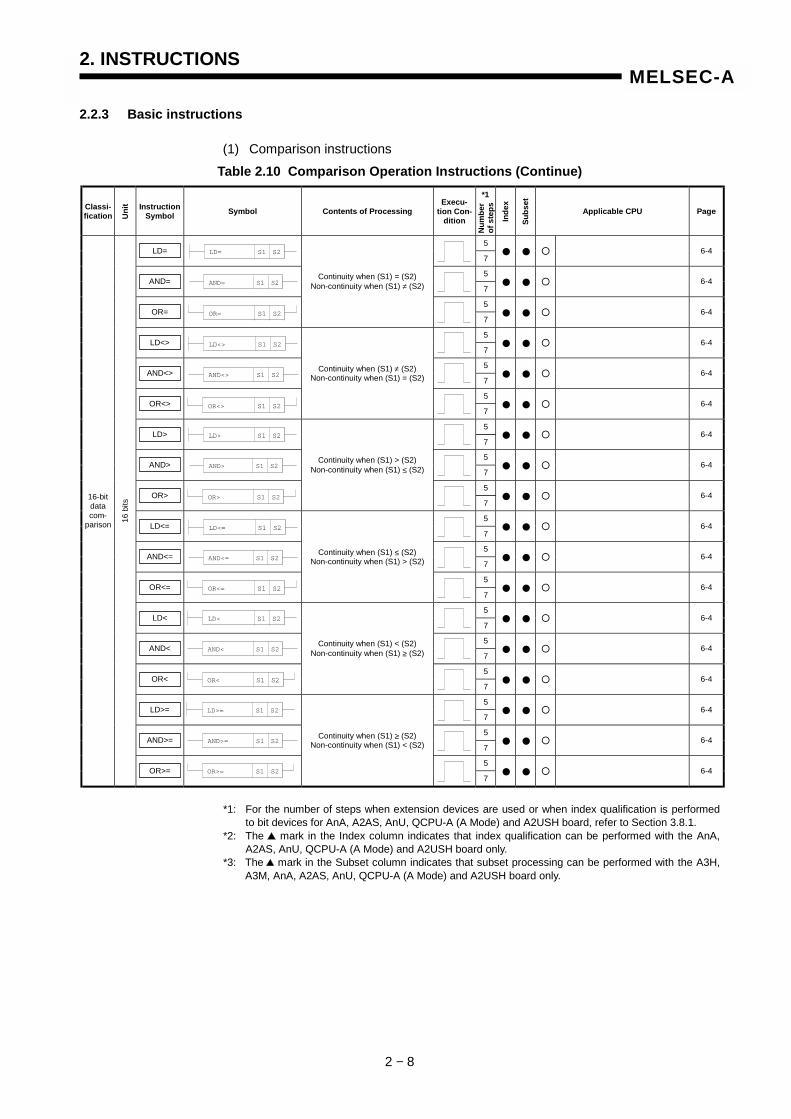
2.2.3 Basic instructions
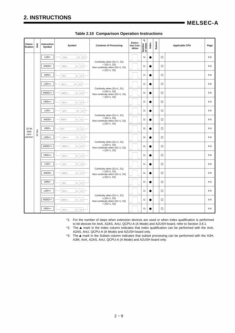
(1) Comparison instructionsTable 2.10 Comparison Operation Instructions (Continue)
Classi-fication U
nit Instruction
Symbol Symbol Contents of ProcessingExecu-
tion Con-dition
Num
ber
of s
teps
Inde
x
Subs
et
Applicable CPU Page
5LD=
7● ● ! 6-4
5AND=
7● ● ! 6-4
5OR=
Continuity when (S1) = (S2)Non-continuity when (S1) ≠ (S2)
7● ● ! 6-4
5LD<>
7● ● ! 6-4
5AND<>
7● ● ! 6-4
5OR<>
Continuity when (S1) ≠ (S2)Non-continuity when (S1) = (S2)
7● ● ! 6-4
5LD>
7● ● ! 6-4
5AND>
7● ● ! 6-4
5OR>
Continuity when (S1) > (S2)Non-continuity when (S1) ≤ (S2)
7● ● ! 6-4
5LD<=
7● ● ! 6-4
5AND<=
7● ● ! 6-4
5OR<=
Continuity when (S1) ≤ (S2)Non-continuity when (S1) > (S2)
7● ● ! 6-4
5LD<
7● ● ! 6-4
5AND<
7● ● ! 6-4
5OR<
Continuity when (S1) < (S2)Non-continuity when (S1) ≥ (S2)
7● ● ! 6-4
5LD>=
7● ● ! 6-4
5AND>=
7● ● ! 6-4
5
16-bitdatacom-
parison 16 b
its
OR>=
Continuity when (S1) ≥ (S2)Non-continuity when (S1) < (S2)
7● ● ! 6-4
*1: For the number of steps when extension devices are used or when index qualification is performedto bit devices for AnA, A2AS, AnU, QCPU-A (A Mode) and A2USH board, refer to Section 3.8.1.
*2: The mark in the Index column indicates that index qualification can be performed with the AnA,A2AS, AnU, QCPU-A (A Mode) and A2USH board only.
*3: The mark in the Subset column indicates that subset processing can be performed with the A3H,A3M, AnA, A2AS, AnU, QCPU-A (A Mode) and A2USH board only.
*1
LD= S1 S2
AND= S1 S2
OR= S1 S2
LD<> S1 S2
AND<> S1 S2
OR<> S1 S2
LD> S1 S2
AND> S1 S2
OR> S1 S2
LD<= S1 S2
AND<= S1 S2
OR<= S1 S2
LD< S1 S2
AND< S1 S2
OR< S1 S2
AND>= S1 S2
OR>= S1 S2
LD>= S1 S2
2. INSTRUCTIONS
2 − 9
MELSEC-A
Table 2.10 Comparison Operation Instructions
Classi-fication U
nit Instruction
Symbol Symbol Contents of ProcessingExecu-
tion Con-dition
Num
ber
of s
teps
Inde
x
Subs
et
Applicable CPU Page
LDD= 11 ● ! 6-6
ANDD= 11 ● ! 6-6
ORD=
Continuity when (S1+1, S1)= (S2+1, S2)
Non-continuity when (S1+1, S1)≠ (S2+1, S2)
11 ● ! 6-6
LDD<> 11 ● ! 6-6
ANDD<> 11 ● ! 6-6
ORD<>
Continuity when (S1+1, S1)≠ (S2+1, S2)
Non-continuity when (S1+1, S1)= (S2+1, S2)
11 ● ! 6-6
LDD> 11 ● ! 6-6
ANDD> 11 ● ! 6-6
ORD>
Continuity when (S1+1, S1)> (S2+1, S2)
Non-continuity when (S1+1, S1)≤ (S2+1, S2)
11 ● ! 6-6
LDD<= 11 ● ! 6-6
ANDD<= 11 ● ! 6-6
ORD<=
Continuity when (S1+1, S1)≤ (S2+1, S2)
Non-continuity when (S1+1, S1)> (S2+1, S2)
11 ● ! 6-6
LDD< 11 ● ! 6-6
ANDD< 11 ● ! 6-6
ORD<
Continuity when (S1+1, S1)< (S2+1, S2)
Non-continuity when (S1+1, S1)≥ (S2+1, S2)
11 ● ! 6-6
LDD>= 11 ● ! 6-6
ANDD>= 11 ● ! 6-6
32 bitdatacom-
parison 32 b
its
ORD>=
Continuity when (S1+1, S1)≥ (S2+1, S2)
Non-continuity when (S1+1, S1)< (S2+1, S2)
11 ● ! 6-6
*1: For the number of steps when extension devices are used or when index qualification is performedto bit devices for AnA, A2AS, AnU, QCPU-A (A Mode) and A2USH board, refer to Section 3.8.1.
*2: The mark in the Index column indicates that index qualification can be performed with the AnA,A2AS, AnU, QCPU-A (A Mode) and A2USH board only.
*3: The mark in the Subset column indicates that subset processing can be performed with the A3H,A3M, AnA, A2AS, AnU, QCPU-A (A Mode) and A2USH board only.
LDD= S1 S2
ANDD= S1 S2
ORD= S1 S2
LDD<> S1 S2
ANDD<> S1 S2
ORD<> S1 S2
LDD> S1 S2
ANDD> S1 S2
ORD> S1 S2
LDD<= S1 S2
ANDD<= S1 S2
ORD<= S1 S2
*1
LDD< S1 S2
ANDD< S1 S2
ORD< S1 S2
LDD>= S1 S2
ANDD>= S1 S2
ORD>= S1 S2
2. INSTRUCTIONS
2 − 10
MELSEC-A
(2) Arithmetic operation instructionTable 2.11 Arithmetic Operation Instruction (Continue)
Classi-fication U
nit Instruction
Symbol Symbol Contents of ProcessingExecu-
tion Con-dition
Num
ber
of s
teps
Inde
x
Subs
et
Applicable CPU Page
+ 5 ●●●● ●●●● ! 6-10
+P
(D) + (S) → (D)
5 ●●●● ●●●● ! 6-10
+ 7 ●●●● ●●●● ! 6-10
+P
(S1) + (S2) → (D)
7 ●●●● ●●●● ! 6-10
- 5 ●●●● ●●●● ! 6-10
-P
(D) - (S) → (D)
5 ●●●● ●●●● ! 6-10
- 7 ●●●● ●●●● ! 6-10
BIN16-bit
addition/subtrac-
tion
16 b
its
-P
(S1) - (S2) → (D)
7 ●●●● ●●●● ! 6-10
D+ 9 ●●●● ●●●● ! 6-13
D+P
(D+1, D) + (S+1, S)→ (D+1, D)
9 ●●●● ●●●● ! 6-13
D+ 11 ●●●● ●●●● ! 6-13
D+P
(S1+1, S1) + (S2+1, S2)→ (D+1, D)
11 ●●●● ●●●● ! 6-13
D- 9 ●●●● ●●●● ! 6-13
D-P
(D+1, D) - (S+1, S) → (D+1, D)
9 ●●●● ●●●● ! 6-13
D- 11 ●●●● ●●●● ! 6-13
BIN32bit
addition/subtrac-
tion
32 b
its
D-P
(S1+1, S1) - (S2+1, S2)→ (D+1, D)
11 ●●●● ●●●● ! 6-13
∗ 7 ●●●● ●●●● ! 6-16
∗ P
(S1) × (S2) → (D+1, D)
7 ●●●● ●●●● ! 6-16
/ 7 ●●●● ●●●● ! 6-16
BIN16bit
multipli-cation/division
16 b
its
/P
(S1) / (S2) → Quotient (D),Remainder (D+1)
7 ●●●● ●●●● ! 6-16
*1: For the number of steps when extension devices are used or when index qualification is performedto bit devices for AnA, A2AS, AnU, QCPU-A (A Mode) and A2USH board, refer to Section 3.8.1.
*2: The mark in the Index column indicates that index qualification can be performed with the AnA,A2AS, AnU, QCPU-A (A Mode) and A2USH board only.
*3: The mark in the Subset column indicates that subset processing can be performed with the A3H,A3M, AnA, A2AS, AnU, QCPU-A (A Mode) and A2USH board only.
*1
* S1 S2 D
+ DS
+P DS
+ DS1 S2
+P DS1 S2
- DS
- P DS
- DS1 S2
- P DS1 S2
D+ S D
D+ S1 S2 D
D+ P S D
D+ P S1 S2 D
D- DS
D- P S D
D- S1 S2 D
D-P S1 S2 D
/ S1 S2 D
/ P S1 S2 D
* S1 S2 DP
2. INSTRUCTIONS
2 − 11
MELSEC-A
Table 2.11 Arithmetic Operation Instruction (Continue)
Classi-fication U
nit Instruction
Symbol Symbol Contents of ProcessingExecu-
tion Con-dition
Num
ber
of s
teps
Inde
x
Subs
et
Applicable CPU Page
D∗ 11 ● ● ! 6-19
D∗ P
(S1+1, S1) × (S2+1, S2)→ (D+3, D+2, D+1, D)
11 ● ● ! 6-19
D/ 11 ● ● ! 6-19
BIN32bit
multipli-cation/division
32 b
its
D/P
(S1+1, S1) / (S2+1, S2) →Quotient (D+1, D),
Remainder (D+3, D+2) 11 ● ● ! 6-19
B+ 7 ● ! 6-22
B+P
(D) + (S) → (D)
7 ● ! 6-22
B+ 9 ● ! 6-22
B+P
(S1) + (S2) → (D)
9 ● ! 6-22
B- 7 ● ! 6-22
B-P
(D) - (S) → (D)
7 ● ! 6-22
B- 9 ● ! 6-22
BCD4-digit
addition/subtrac-
tion BCD
4-d
igits
B-P
(S1) - (S2) → (D)
9 ● ! 6-22
DB+ 9 ● ! 6-25
DB+P
(D+1, D) + (S+1, S)→ (D+1, D)
9 ● ! 6-25
DB+ 11 ● ! 6-25
BCD8-digit
additionsubtrac-
tion BCD
8-d
igits
DB+P
(S1+1, S1) + (S2+1, S2))→ (D+1, D)
11 ● ! 6-25
DB- 9 ● ! 6-25
DB-P
(D+1, D) - (S+1, S)→ (D+1, D)
9 ● ! 6-25
DB- 11 ● ! 6-25
BCD8-digit
addition,subtrac-
tion BCD
8-d
igits
DB-P
(S1+1, S1) - (S2+1, S)→ (D+1, D)
11 ● ! 6-25
*1: For the number of steps when extension devices are used or when index qualification is performedto bit devices for AnA, A2AS, AnU, QCPU-A (A Mode) and A2USH board, refer to Section 3.8.1.
*2: The mark in the Index column indicates that index qualification can be performed with the AnA,A2AS, AnU, QCPU-A (A Mode) and A2USH board only.
*3: The mark in the Subset column indicates that subset processing can be performed with the A3H,A3M, AnA, A2AS, AnU, QCPU-A (A Mode) and A2USH board only.
*1
*3
*3
*3
*3
D/ S1 S2 D
D/ P S1 S2 D
B+ DS
B+P S D
B+ S1 S2 D
B+P S1 S2 D
B- DS
B-P S D
B- S1 S2 D
B- P S1 S2 D
DB+ S D
DB+P S D
DB+ S1 S2 D
DB+P S1 S2 D
DB- S D
DB- P S D
DB- S1 S2 D
DB- P S1 S2 D
D S1 S2 D*
D P S1 S2 D*

2. INSTRUCTIONS
2 − 12
MELSEC-A
B S1 S2 D*
Table 2.11 Arithmetic Operation Instructions
Classi-fication U
nit Instruction
Symbol Symbol Contents of ProcessingExecu-
tion Con-dition
Num
ber
of s
teps
Inde
x
Subs
et
Applicable CPU Page
B∗ 9 ● ! 6-28
B∗ P
(S1) × (S2) → (D+1, D)
9 ● ! 6-28
B/ 9 ● ! 6-28
BCD4-digit
multipli-cation,division BC
D 4
-dig
its
B/P
(S1) / (S2) → Quotient (D)|Remainder (D+1)
9 ● ! 6-28
DB∗ 11 ● ! 6-31
DB∗ P
(S1+1, S1) × (S2+1, S2)→ (D+3, D+2, D+1, D)
11 ● ! 6-31
DB/ 11 ● ! 6-31
BCD8-digit
multipli-cation,division BC
D 8
-dig
its
DB/P
(S1+1, S1) / (S2+1, S2)→Quotient (D+1, D),
Remainder (D+3, D+2) 11 ● ! 6-31
INC 3 ● ● ! 6-34
16 b
its
INCP
(D) +1 → (D)
3 ● ● ! 6-34
DINC 3 ● ● ! 6-36
BINdataincre-ment
32 b
its
DINCP
(D+1, D) +1 → (D+1, D)
3 ● ● ! 6-36
DEC 3 ● ● ! 6-34
16 b
its
DECP
(D) -1 → (D)
3 ● ● ! 6-34
DDEC 3 ● ● ! 6-36
BINdata
decre-ment
32 b
its
DDECP
(D+1, D) -1 → (D+1, D)
3 ● ● ! 6-36
*1: For the number of steps when extension devices are used or when index qualification is performedto bit devices for AnA, A2AS, AnU, QCPU-A (A Mode) and A2USH board, refer to Section 3.8.1.
*2: The mark in the Index column indicates that index qualification can be performed with the AnA,A2AS, AnU, QCPU-A (A Mode) and A2USH board only.
*3: The mark in the Subset column indicates that subset processing can be performed with the A3H,A3M, AnA, A2AS, AnU, QCPU-A (A Mode) and A2USH board only.
*1
*3
*3
*3
*3
B/ S1 S2 D
B/ P S1 S2 D
DB/ P S1 S2 D
DB/ S1 S2 D
INC D
INCP D
DINC D
DINCP D
DEC D
DECP D
DDEC D
DDECP D
B P S1 S2 D*
DB S1 S2 D*
DB P S1 S2 D*
2. INSTRUCTIONS
2 − 13
MELSEC-A
(3) BCD ↔ BIN conversion instructions
Table 2.12 BCD ↔↔↔↔ BIN Conversion Instructions
Classi-fication U
nit Instruction
Symbol Symbol Contents of ProcessingExecu-
tion Con-dition
Num
ber
of s
teps
Inde
x
Subs
et
Applicable CPU Page
BCD 5 ● ● ! 6-39
16 b
its
BCDP
BCD conversion
(S) (D)
BIN (0 to 9999) 5 ● ● ! 6-39
DBCD 9 ● ! 6-39
BCDconver-
sion
32 b
its
DBCDP
BCD conversion
(S1+1, S1) (D+1, D)
BIN (0 to 99999999) 9 ● ! 6-39
BIN 5 ● ● ! 6-42
4-di
gits
BINP
BIN conversion
(S) (D)
BCD(0 to 9999) 5 ● ● ! 6-42
DBIN 9 ● ! 6-42
BINconver-
sion
8-di
gits
DBINP
BIN conversion
(S1+1, S1) (D+1, D)
BCD (0 to 99999999) 9 ● ! 6-42
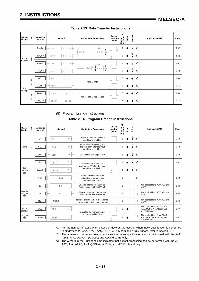
(4) Data transfer instructionsTable 2.13 Data Transfer Instructions (Continue)
Classi-fication U
nit Instruction
Symbol Symbol Contents of ProcessingExecu-
tion Con-dition
Num
ber
of s
teps
Inde
x
Subs
etApplicable CPU Page
MOV 5 ● ● ! 6-47
16 b
its
MOVP
(S) → (D)
5 ● ● ! 6-47
DMOV 7 ● ● ! 6-47
Transfer
32 b
its
DMOVP
(S+1, S) → (D+1, D)
7 ● ● ! 6-47
CML 5 ● ● ! 6-49
16 b
its
CMLP
(S) → (D)
5 ● ● ! 6-49
DCML 7 ● ● ! 6-49
Nega-tion
transfer
32 b
its
DCMLP
(S+1, S) → (D+1, D)
7 ● ● ! 6-49
*1: For the number of steps when extension devices are used or when index qualification is performedto bit devices for AnA, A2AS, AnU, QCPU-A (A Mode) and A2USH board, refer to Section 3.8.1.
*2: The mark in the Index column indicates that index qualification can be performed with the AnA,A2AS, AnU, QCPU-A (A Mode) and A2USH board only.
*3: The mark in the Subset column indicates that subset processing can be performed with the A3H,A3M, AnA, A2AS, AnU, QCPU-A (A Mode) and A2USH board only.
*1
*3
*3
*1
BCD S D
BCDP S D
DBCD DS
DBCDP S D
BIN S D
BINP S D
DBIN S D
DBINP S D
MOV S D
MOVP S D
DMOV S D
DMOVP S D
CML S D
CMLP S D
DCML S D
DCMLP S D
2. INSTRUCTIONS
2 − 14
MELSEC-A
Table 2.13 Data Transfer Instructions
Classi-fication U
nit Instruction
Symbol Symbol Contents of ProcessingExecu-
tion Con-dition
Num
ber
of s
teps
Inde
x
Subs
et
Applicable CPU Page
BMOV 9 ● ! 6-52
BMOVP 9 ● ! 6-52
FMOV 9 ● ! 6-52
Blocktransfer 16
bits
FMOVP 9 ● ! 6-52
XCH 5 ● ● ! 6-56
16 b
its
XCHP
(D1) ↔ (D2)
5 ● ● ! 6-56
DXCH 7 ● ● ! 6-56
Ex-change
32 b
its
DXCHP
(D1+1, D1) ↔ (D2+1, D2)
7 ● ● ! 6-56
(5) Program branch instructionsTable 2.14 Program Branch Instructions
Classi-fication U
nit Instruction
Symbol Symbol Contents of ProcessingExecu-
tion Con-dition
Num
ber
of s
teps
Inde
x
Subs
etApplicable CPU Page
CJ Jumps to P** after the inputcondition is enabled. 3 ● ! 6-58
SCJJumps to P ** beginning withthe next scan after the input
condition is enabled.3 ● ! 6-58Jump
JMP Unconditionally jumps to P** 3 ● ! 6-58
CALL 3 ● ! 6-62
CALLP
Executes the subroutineprogram at P** after the input
condition is enabled.3 ● !
Sub-routine
call
RETReturns execution from thesubroutine program to the
sequence program.1 ! 6-62
EI Enables interrupt program run.Valid for AnN with M9053 off. 1 Not applicable to A3V, A2C and
A52G. 6-64
DI Disables interrupt program run.Valid for AnN with M9053 off. 1 Not applicable to A3V, A2C and
A52G. 6-64Interruptprogram
call
IRET Returns execution from the interruptprogram to the sequence program. 1 Not applicable to A3V, A2C and
A52G. 6-64
SUB 3 ●Not applicable to AnA, A2AS,AnU, QCPU-A (A Mode) andA2USH board.
6-67Micro-comput-
erprogram
call
SUBP
Executes the microcomputerprogram specified by n.
3 ●Not applicable to AnA, A2AS,AnU, QCPU-A (A Mode) andA2USH board.
6-67
*1: For the number of steps when extension devices are used or when index qualification is performedto bit devices for AnA, A2AS, AnU, QCPU-A (A Mode) and A2USH board, refer to Section 3.8.1.
*2: The mark in the Index column indicates that index qualification can be performed with the AnA,A2AS, AnU, QCPU-A (A Mode) and A2USH board only.
*3: The mark in the Subset column indicates that subset processing can be performed with the A3H,A3M, AnA, A2AS, AnU, QCPU-A (A Mode) and A2USH board only.
*1
*3
*3
*3
*3
*1
*3
*3
*3
*3
*3
n
(S) (D)
n(S)
(D)
BMOV nS D
BMOVP nS D
FMOV nS D
FMOVP nS D
XCH D1 D2
XCHP D1 D2
DXCH D1 D2
DXCHP D1 D2
CJ P**
SCJ P**
CALL P**
CALLP P**
EI
DI
IRET
SUB n
SUBP n
JMP P**
RET
2. INSTRUCTIONS
2 − 15
MELSEC-A
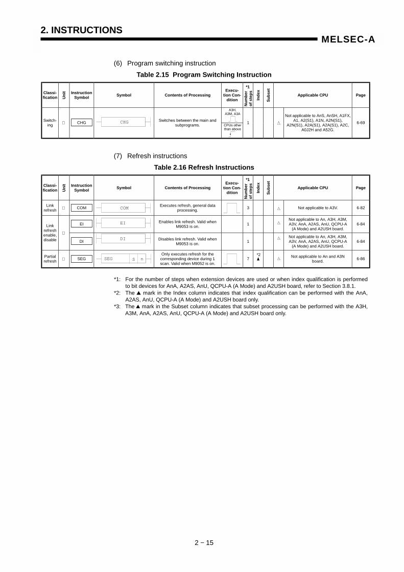
(6) Program switching instructionTable 2.15 Program Switching Instruction
Classi-fication U
nit Instruction
Symbol Symbol Contents of ProcessingExecu-
tion Con-dition
Num
ber
of s
teps
Inde
x
Subs
et
Applicable CPU Page
Switch-ing CHG Switches between the main and
subprograms. 1
Not applicable to AnS, AnSH, A1FX,A1, A2(S1), A1N, A2N(S1),
A2N(S1), A2A(S1), A2A(S1), A2C,A0J2H and A52G.
6-69
(7) Refresh instructionsTable 2.16 Refresh Instructions
Classi-fication U
nit Instruction
Symbol Symbol Contents of ProcessingExecu-
tion Con-dition
Num
ber
of s
teps
Inde
x
Subs
et
Applicable CPU Page
Linkrefresh COM Executes refresh, general data
processing. 3 Not applicable to A3V. 6-82
EI Enables link refresh. Valid whenM9053 is on. 1
Not applicable to An, A3H, A3M,A3V, AnA, A2AS, AnU, QCPU-A
(A Mode) and A2USH board.6-84Link
refreshenable,disable
DI Disables link refresh. Valid whenM9053 is on. 1
Not applicable to An, A3H, A3M,A3V, AnA, A2AS, AnU, QCPU-A
(A Mode) and A2USH board.6-84
Partialrefresh SEG
Only executes refresh for thecorresponding device during 1scan. Valid when M9052 is on.
7 Not applicable to An and A3Nboard. 6-86
*1: For the number of steps when extension devices are used or when index qualification is performedto bit devices for AnA, A2AS, AnU, QCPU-A (A Mode) and A2USH board, refer to Section 3.8.1.
*2: The mark in the Index column indicates that index qualification can be performed with the AnA,A2AS, AnU, QCPU-A (A Mode) and A2USH board only.
*3: The mark in the Subset column indicates that subset processing can be performed with the A3H,A3M, AnA, A2AS, AnU, QCPU-A (A Mode) and A2USH board only.
*1
A3H,A3M, A3A
CPUs otherthan above
CHG
*1
*2
COM
EI
DI
SEG nS

2. INSTRUCTIONS
2 − 16
MELSEC-A
2.2.4 Application instructions
(1) Logical operation instructionsTable 2.17 Logical Operation Instructions
Classi-fication U
nit Instruction
Symbol Symbol Contents of ProcessingExecu-
tion Con-dition
Num
ber
of s
teps
Inde
x
Subs
et
Applicable CPU Page
WAND 5 ● ● ! 7-3
WANDP
(D) AND (S) → (D)
5 ● ● ! 7-3
WAND 7 ● ! 7-3
16 b
its
WANDP
(S1) AND (S2) → (D)
7 ● ! 7-3
DAND 9 ● ! 7-3
Logicalproduct
32 b
its
DANDP
(D+1, D) AND (S+1, S)→(D+1,D)
9 ● ! 7-3
WOR 5 ● ● ! 7-7
WORP
(D) OR (S) → (D)
5 ● ● ! 7-7
WOR 7 ● ! 7-7
16bi
ts
WORP
(S1) OR (S2) → (D)
7 ● ! 7-7
DOR 9 ● ! 7-7
Logicalsum
32 b
its
DORP
(D+1, D) OR (S+1, S)→ (D+1, D)
9 ● ! 7-7
WXOR 5 ● ● ! 7-11
WXORP
(D) XOR (S) → (D)
5 ● ● ! 7-11
WXOR 7 ● ! 7-11
16 b
its
WXORP
(S1) XOR (S2) → (D)
7 ● ! 7-11
DXOR 9 ● ! 7-11
Exclu-sive
logicalsum
32 b
its
DXORP
(D+1, D) XOR (S+1, S)→ (D+1, D)
9 ● ! 7-11
*1: For the number of steps when extension devices are used or when index qualification is performedto bit devices for AnA, A2AS, AnU, QCPU-A (A Mode) and A2USH board, refer to Section 3.8.1.
*2: The mark in the Index column indicates that index qualification can be performed with the AnA,A2AS, AnU, QCPU-A (A Mode) and A2USH board only.
*3: The mark in the Subset column indicates that subset processing can be performed with the A3H,A3M, AnA, A2AS, AnU, QCPU-A (A Mode) and A2USH board only.
*1
WAND S D
WANDP S D
WAND S1 S2 D
WANDP S1 S2 D
DAND S D
DANDP S D
WOR S D
WORP DS
WOR S1 S2 D
WORP S1 S2 D
DOR DS
DORP S D
WXOR S D
WXORP S D
WXOR S1 S2 D
WXORP S1 S2 D
DXOR S D
DXORP DS

2. INSTRUCTIONS
2 − 17
MELSEC-A
Table 2.17 Logical Operation Instructions (Continue)
Classi-fication U
nit Instruction
Symbol Symbol Contents of ProcessingExecu-
tion Con-dition
Num
ber
of s
teps
Inde
x
Subs
et
Applicable CPU Page
WXNR 5 ● ● ! 7-15
WXNRP
(D) XOR (S) → (D)
5 ● ● ! 7-15
WXNR 7 ● ! 7-15
16 b
its
WXNRP
(S1) XOR (S2) → (D)
7 ● ! 7-15
DXNR 9 ● ! 7-15
NOTexclu-sive
logicalsum
32 b
its
DXNRP
(D+1, D) XOR (S+1, S)→ (D+1, D)
9 ● ! 7-15
NEG 3 ● ! 7-192’scomple-
ment
16 b
its
NEGP
0- (D) → (D)
3 ● ! 7-19
*1: For the number of steps when extension devices are used or when index qualification is performedto bit devices for AnA, A2AS, AnU, QCPU-A (A Mode) and A2USH board, refer to Section 3.8.1.
*2: The mark in the Index column indicates that index qualification can be performed with the AnA,A2AS, AnU, QCPU-A (A Mode) and A2USH board only.
*3: The mark in the Subset column indicates that subset processing can be performed with the A3H,A3M, AnA, A2AS, AnU, QCPU-A (A Mode) and A2USH board only.
*1
NEG D
NEGP D
WXNR DS
WXNRP DS
WXNR S1 S2 D
WXNRP S1 S2 D
DXNR DS
DXNRP DS
2. INSTRUCTIONS
2 − 18
MELSEC-A
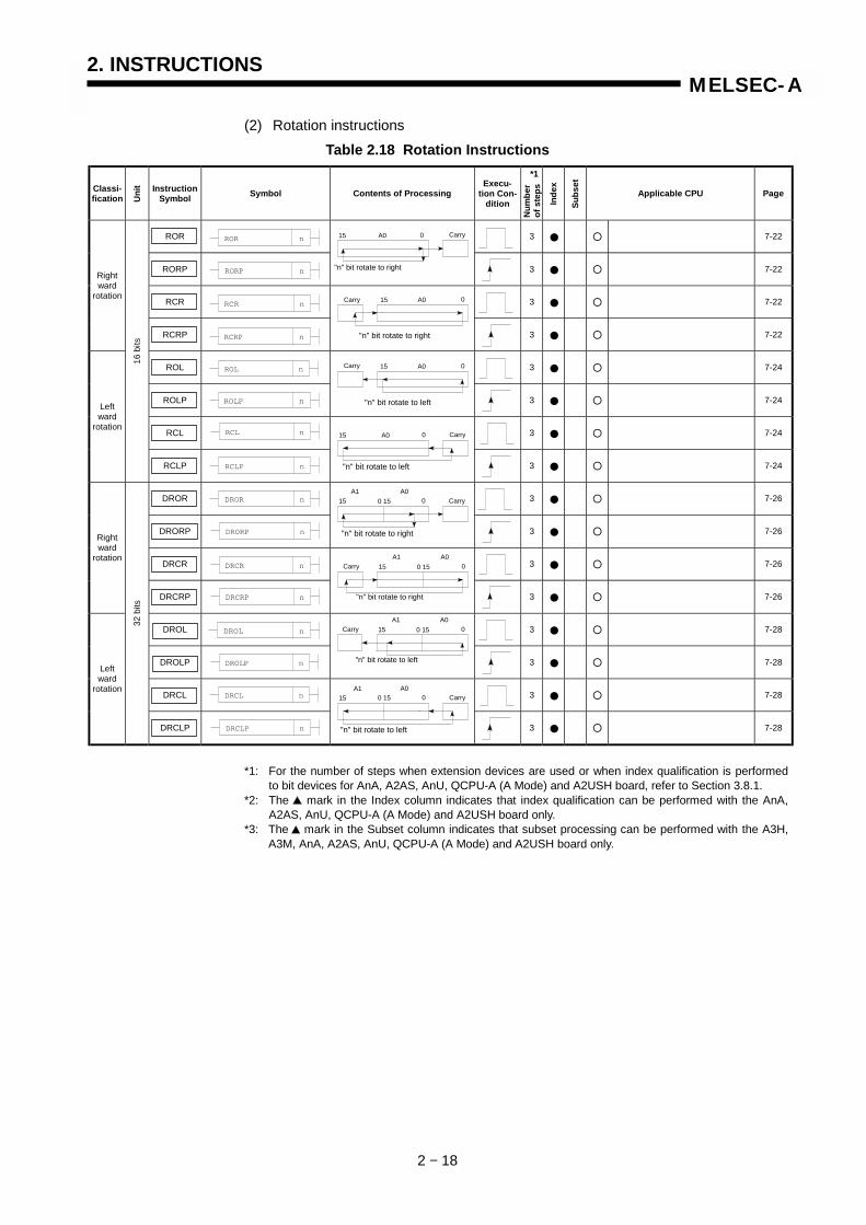
015 Carry0 15A1 A0
"n" bit rotate to left
(2) Rotation instructionsTable 2.18 Rotation Instructions
Classi-fication U
nit Instruction
Symbol Symbol Contents of ProcessingExecu-
tion Con-dition
Num
ber
of s
teps
Inde
x
Subs
et
Applicable CPU Page
ROR 3 ● ! 7-22
RORP 3 ● ! 7-22
RCR 3 ● ! 7-22
Rightward
rotation
RCRP 3 ● ! 7-22
ROL 3 ● ! 7-24
ROLP 3 ● ! 7-24
RCL 3 ● ! 7-24
Leftward
rotation
16 b
its
RCLP 3 ● ! 7-24
DROR 3 ● ! 7-26
DRORP 3 ● ! 7-26
DRCR 3 ● ! 7-26
Rightward
rotation
DRCRP 3 ● ! 7-26
DROL 3 ● ! 7-28
DROLP 3 ● ! 7-28
DRCL 3 ● ! 7-28
Leftward
rotation
32 b
its
DRCLP 3 ● ! 7-28
*1: For the number of steps when extension devices are used or when index qualification is performedto bit devices for AnA, A2AS, AnU, QCPU-A (A Mode) and A2USH board, refer to Section 3.8.1.
*2: The mark in the Index column indicates that index qualification can be performed with the AnA,A2AS, AnU, QCPU-A (A Mode) and A2USH board only.
*3: The mark in the Subset column indicates that subset processing can be performed with the A3H,A3M, AnA, A2AS, AnU, QCPU-A (A Mode) and A2USH board only.
*1
RCR n
ROR n
RORP n
RCRP n
ROL n
ROLP n
RCL n
RCLP n
DROR n
DRORP n
DRCR n
DRCRP n
DROLP n
DROL n
DRCL n
"n" bit rotate to right
CarryA0 015
Carry A0 0 15
"n" bit rotate to right
Carry A0 0 15
"n" bit rotate to left
015 CarryA0
"n" bit rotate to left
015 Carry0 15A1 A0
"n" bit rotate to right
A1 A0 015Carry 0 15
"n" bit rotate to right
A1 A0 015Carry 0 15
"n" bit rotate to left
DRCLP n

2. INSTRUCTIONS
2 − 19
MELSEC-A
(3) Shift instructionsTable 2.19 Shift Instructions
Classi-fication U
nit Instruction
Symbol Symbol Contents of ProcessingExecu-
tion Con-dition
Num
ber
of s
teps
Inde
x
Subs
et
Applicable CPU Page
SFR 5 ● ● ! 7-31
SFRP 5 ● ● ! 7-31
SFL 5 ● ● ! 7-31
n bitshift 16
bits
SFLP 5 ● ● ! 7-31
BSFR 7 ● ! 7-33
BSFRP 7 ● ! 7-33
BSFL 7 ● ! 7-33
1 bitshift n
bit
BSFLP 7 ● ! 7-33
DSFR 7 ● Not applicable to A73 7-35
DSFRP 7 ● Not applicable to A73 7-35
DSFL 7 ● Not applicable to A73 7-35
1 wardshift n
war
d
DSFLP 7 ● Not applicable to A73 7-35
*1: For the number of steps when extension devices are used or when index qualification is performedto bit devices for AnA, A2AS, AnU, QCPU-A (A Mode) and A2USH board, refer to Section 3.8.1.
*2: The mark in the Index column indicates that index qualification can be performed with the AnA,A2AS, AnU, QCPU-A (A Mode) and A2USH board only.
*3: The mark in the Subset column indicates that subset processing can be performed with the A3H,A3M, AnA, A2AS, AnU, QCPU-A (A Mode) and A2USH board only.
*1
*3
*3
*3
*3
0n15
0 to 0
0 Carry15to
BSFRP nD
BSFLP nD
DSFLP nD
DSFRP D n
SFR nD
SFL nD
BSFR nD
BSFL nD
DSFR nD
DSFL nD
Carry
15 n 0
0 to 0
15 0to
SFRP nD
SFLP nD
(D)
n
Carry
0
to
(D)
n
0
to
(D)
n
0
to
n
(D)
Carryto
0
2. INSTRUCTIONS
2 − 20
MELSEC-A
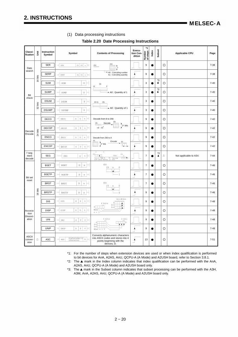
(1) Data processing instructionsTable 2.20 Date Processing Instructions
Classi-fication U
nit Instruction
Symbol Symbol Contents of ProcessingExecu-
tion Con-dition
Num
ber
of s
teps
Inde
x
Subs
et
Applicable CPU Page
SER 9 ● ! 7-38Date
searchSERP 9 ● ! 7-38
SUM 3 ● ! 7-40
16 b
its
SUMP 3 ● ! 7-40
DSUM 3 ● ! 7-40
Bitcheck
32 b
its
DSUMP 3 ● ! 7-40
DECO 9 ● ! 7-42
DECOP 9 ● ! 7-42
ENCO 9 ● ! 7-42
DecodeEncode 2n
bits
ENCOP 9 ● ! 7-42
7.seg-ment
decodeSEG 7 ● Not applicable to A3V. 7-44
BSET 7 ● ! 7-46
BSETP 7 ● ! 7-46
BRST 7 ● ! 7-46
Bit setreset
BRSTP 9 ● ! 7-46
DIS 9 ● ! 7-48
DISP 9 ● ! 7-48
UNI 9 ● ! 7-48
Accocia-tion
Dissoci-ation
16 b
its
UNIP 9 ● ! 7-48
ASCIIconver-
sion ASC
Converts alphanumeric charactersinto ASCII codes and stores into 4
points beginning with thedevices, D.
13 ● ! 7-51
*1: For the number of steps when extension devices are used or when index qualification is performedto bit devices for AnA, A2AS, AnU, QCPU-A (A Mode) and A2USH board, refer to Section 3.8.1.
*2: The mark in the Index column indicates that index qualification can be performed with the AnA,A2AS, AnU, QCPU-A (A Mode) and A2USH board only.
*3: The mark in the Subset column indicates that subset processing can be performed with the A3H,A3M, AnA, A2AS, AnU, QCPU-A (A Mode) and A2USH board only.
Decode from 256 to 8
2n bitsEncode(S)
(D)
n
Decode from 8 to 256(D)
(S)
n 2n bitsDecode
*3
*1
*3A0 : Quantity of 1
015(S)
SUMP S
A0 : Quantity of 1
(S)(S+1)
DSUMP S
DECOP nDS
ENCOP nDS
SERP nS1 S2
SER nS1 S2
SUM S
DSUM S
DECO nDS
ENCO nDS
*3
15(D)
0n
1
15
(D)
0n
0
4 bits
D4 bits
All 0
D+1D+2S
Whenn = 3
DISP nS D
4 bits
S
4 bits
S+1S+2
D
When n = 3UNIP nS D
ASC DAlphanumericcharacter
SEG nS
DIS nS D
UNI nS D
BSET D n
BSETP D n
BRST D n
BRSTP D n
A0 : Coinciding numberA1 : Coinciding quantity
(S2)
n(S1)
Valid for A N. DecodeA3H when M9052 is off.
7SEG(D)
n 0(S)
3 0

2. INSTRUCTIONS
2 − 21
MELSEC-A
(5) FIFO instructionsTable 2.21 FIFO Instructions
Classi-fication U
nit Instruction
Symbol Symbol Contents of ProcessingExecu-
tion Con-dition
Num
ber
of s
teps
Inde
x
Subs
et
Applicable CPU Page
FIFW 7 ● ! 7-54
Write
FIFWP 7 ● ! 7-54
FIFR 7 ● ! 7-54
Read
16 b
its
FIFRP 7 ● ! 7-54
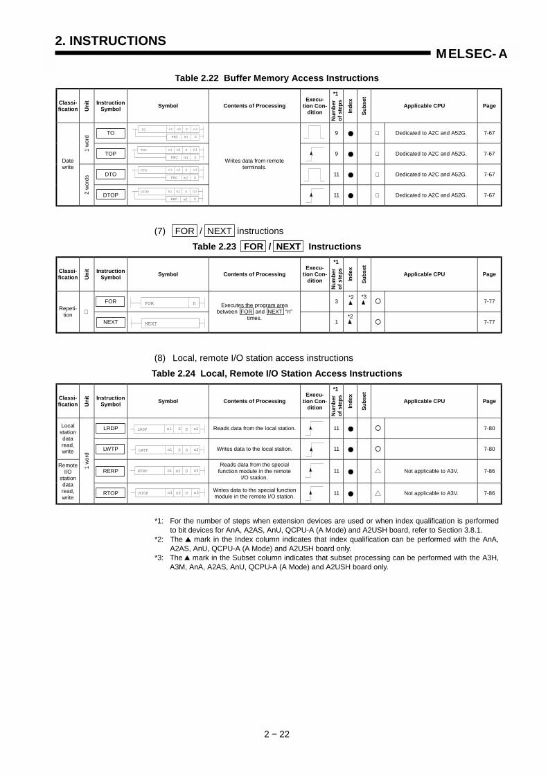
(6) Buffer memory Access instructionsTable 2.22 Buffer Memory Access Instruction (Continue)
Classi-fication U
nit Instruction
Symbol Symbol Contents of ProcessingExecu-
tion Con-dition
Num
ber
of s
teps
Inde
x
Subs
et
Applicable CPU Page
FROM 9 ● Not applicable to A2C and A52G. 7-59
1 w
ord
FROMP 9 ● Not applicable to A2C and A52G. 7-59
DFRO 9 ● Not applicable to A2C and A52G. 7-59
Dateread
2 w
ords
DFROP
Reads data from the specialfunction module.
9 ● Not applicable to A2C and A52G. 7-59
TO 9 ● Not applicable to A2C and A52G. 7-61
1 w
ord
TOP 9 ● Not applicable to A2C and A52G. 7-61
DTO 11 ● Not applicable to A2C and A52G. 7-61
Datewrite
2 w
ords
DTOP
Writes data to the specialfunction module.
11 ● Not applicable to A2C and A52G. 7-61
FROM 9 ● Dedicated to A2C and A52G. 7-63
1 w
ord
FROMP 9 ● Dedicated to A2C and A52G. 7-63
DFRO 9 ● Dedicated to A2C and A52G. 7-63
Dataread
2 w
ords
DFROP
Reads data from remoteterminals.
9 ● Dedicated to A2C and A52G. 7-63
*1: For the number of steps when extension devices are used or when index qualification is performedto bit devices for AnA, A2AS, AnU, QCPU-A (A Mode) and A2USH board, refer to Section 3.8.1.
*2: The mark in the Index column indicates that index qualification can be performed with the AnA,A2AS, AnU, QCPU-A (A Mode) and A2USH board only.
*3: The mark in the Subset column indicates that subset processing can be performed with the A3H,A3M, AnA, A2AS, AnU, QCPU-A (A Mode) and A2USH board only.
*1
*1
(S)
(D) Pointer
Pointer
+1
(D2) Pointer Pointer-1
(D1)
FIFW S D
FIFWP S D
FIFR D1 D2
FIFRP D1 D2
FROM n3n1 n2 D
FROMP n3n1 n2 D
DFRO n3n1 n2 D
DFROP n3n1 n2 D
TO n3n1 n2 S
TOP n3n1 n2 S
DTO n3n1 n2 S
DTOP n3n1 n2 D
FROM n3n1 n2 D
nPRC m1
FROMP n3n1 n2 D
nPRC m1
DFROP n3n1 n2 D
nPRC m1
DFRO n3n1 n2 D
nPRC m1
2. INSTRUCTIONS
2 − 22
MELSEC-A
Table 2.22 Buffer Memory Access Instructions
Classi-fication U
nit Instruction
Symbol Symbol Contents of ProcessingExecu-
tion Con-dition
Num
ber
of s
teps
Inde
x
Subs
et
Applicable CPU Page
TO 9 ● Dedicated to A2C and A52G. 7-67
1 w
ord
TOP 9 ● Dedicated to A2C and A52G. 7-67
DTO 11 ● Dedicated to A2C and A52G. 7-67
Datewrite
2 w
ords
DTOP
Writes data from remoteterminals.
11 ● Dedicated to A2C and A52G. 7-67
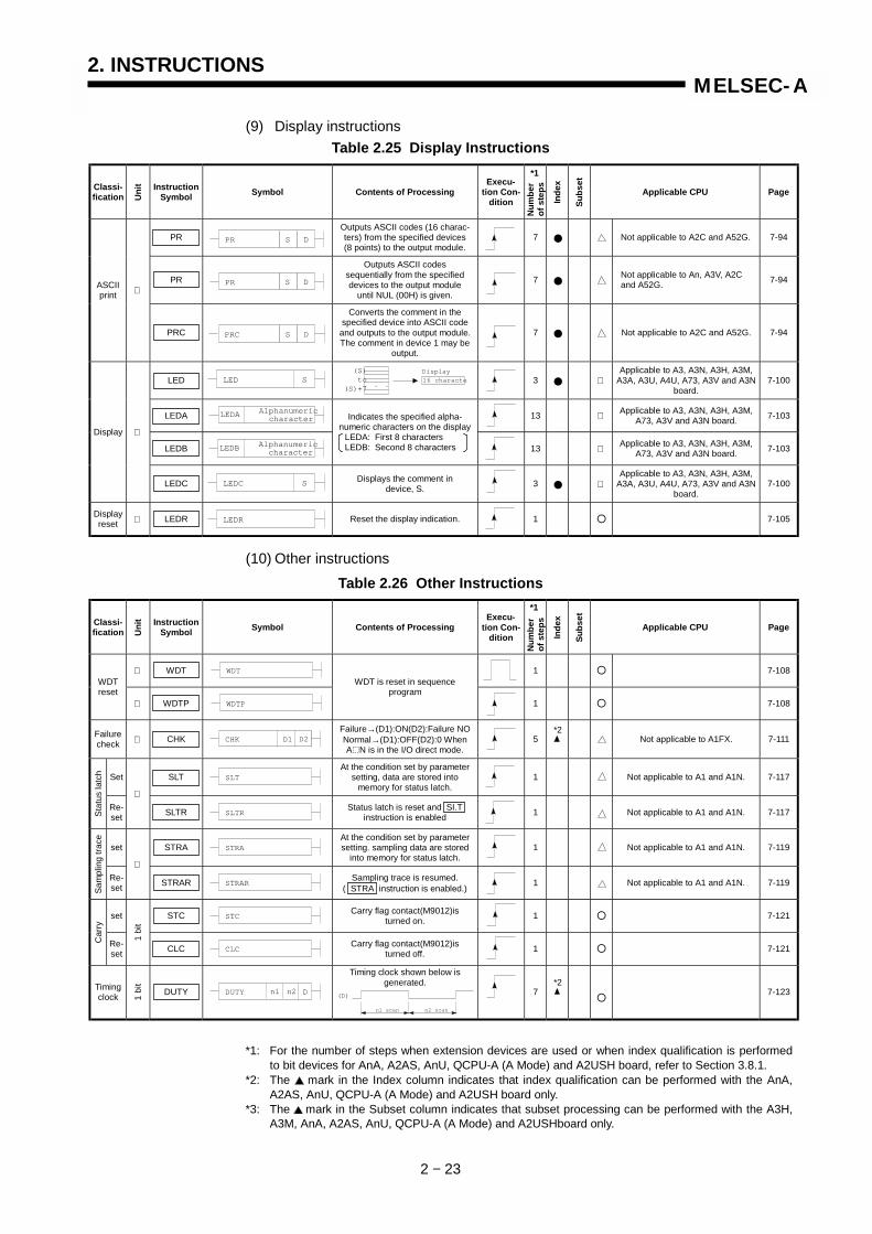
(7) FOR / NEXT instructionsTable 2.23 FOR / NEXT Instructions
Classi-fication U
nit Instruction
Symbol Symbol Contents of ProcessingExecu-
tion Con-dition
Num
ber
of s
teps
Inde
x
Subs
et
Applicable CPU Page
FOR 3 ! 7-77Repeti-
tion
NEXT
Executes the program areabetween FOR and NEXT “n”
times.1 ! 7-77
(8) Local, remote I/O station access instructionsTable 2.24 Local, Remote I/O Station Access Instructions
Classi-fication U
nit Instruction
Symbol Symbol Contents of ProcessingExecu-
tion Con-dition
Num
ber
of s
teps
Inde
x
Subs
et
Applicable CPU Page
LRDP Reads data from the local station. 11 ● ! 7-80Localstationdataread,write LWTP Writes data to the local station. 11 ● ! 7-80
RERPReads data from the special
function module in the remoteI/O station.
11 ● Not applicable to A3V. 7-86Remote
I/Ostationdataread,write
1 w
ord
RTOP Writes data to the special functionmodule in the remote I/O station. 11 ● Not applicable to A3V. 7-86
*1: For the number of steps when extension devices are used or when index qualification is performedto bit devices for AnA, A2AS, AnU, QCPU-A (A Mode) and A2USH board, refer to Section 3.8.1.
*2: The mark in the Index column indicates that index qualification can be performed with the AnA,A2AS, AnU, QCPU-A (A Mode) and A2USH board only.
*3: The mark in the Subset column indicates that subset processing can be performed with the A3H,A3M, AnA, A2AS, AnU, QCPU-A (A Mode) and A2USH board only.
*2
*1
*2
*3
*1
FOR n
NEXT
LRDP n2n1 S D
LWTP n2n1 D S
RFRP n3n1 n2 D
RTOP n3n1 n2 D
TO n3n1 n2 S
nPRC m1
TOP n3n1 n2 S
nPRC m1
DTO n3n1 n2 S
nPRC m1
DTOP n3n1 n2 S
nPRC m1
*1
2. INSTRUCTIONS
2 − 23
MELSEC-A
(9) Display instructionsTable 2.25 Display Instructions
Classi-fication U
nit Instruction
Symbol Symbol Contents of ProcessingExecu-
tion Con-dition
Num
ber
of s
teps
Inde
x
Subs
et
Applicable CPU Page
PROutputs ASCII codes (16 charac-ters) from the specified devices(8 points) to the output module.
7 ● Not applicable to A2C and A52G. 7-94
PR
Outputs ASCII codessequentially from the specifieddevices to the output module
until NUL (00H) is given.
7 ●Not applicable to An, A3V, A2Cand A52G. 7-94ASCII
PRC
Converts the comment in thespecified device into ASCII code
and outputs to the output module.The comment in device 1 may be
output.
7 ● Not applicable to A2C and A52G. 7-94
LED 3 ● Applicable to A3, A3N, A3H, A3M,
A3A, A3U, A4U, A73, A3V and A3Nboard.
7-100
LEDA 13 Applicable to A3, A3N, A3H, A3M,A73, A3V and A3N board. 7-103
LEDB
Indicates the specified alpha-numeric characters on the display
LEDA: First 8 charactersLEDB: Second 8 characters 13 Applicable to A3, A3N, A3H, A3M,
A73, A3V and A3N board. 7-103
Display
LEDC Displays the comment indevice, S. 3 ●
Applicable to A3, A3N, A3H, A3M,A3A, A3U, A4U, A73, A3V and A3N
board.7-100
Displayreset LEDR Reset the display indication. 1 ! 7-105
(10) Other instructionsTable 2.26 Other Instructions
Classi-fication U
nit Instruction
Symbol Symbol Contents of ProcessingExecu-
tion Con-dition
Num
ber
of s
teps
Inde
x
Subs
et
Applicable CPU Page
WDT 1 ! 7-108WDTreset
WDTP
WDT is reset in sequenceprogram
1 ! 7-108
Failurecheck CHK
Failure→(D1):ON(D2):Failure NONormal→(D1):OFF(D2):0 WhenA N is in the I/O direct mode.
5 Not applicable to A1FX. 7-111
Set SLTAt the condition set by parameter
setting, data are stored intomemory for status latch.
1 Not applicable to A1 and A1N. 7-117
Stat
us la
tch
Re-set
SLTR Status latch is reset and SI.Tinstruction is enabled 1 Not applicable to A1 and A1N. 7-117
set STRAAt the condition set by parametersetting. sampling data are stored
into memory for status latch.1 Not applicable to A1 and A1N. 7-119
Sam
plin
g tra
ce
Re-set
STRAR Sampling trace is resumed.( STRA instruction is enabled.) 1 Not applicable to A1 and A1N. 7-119
set STC Carry flag contact(M9012)isturned on. 1 ! 7-121
Car
ry
Re-set
1 bi
t
CLC Carry flag contact(M9012)isturned off. 1 ! 7-121
Timingclock 1
bit
DUTY
Timing clock shown below isgenerated.
7!
7-123
*1
*2
PR S D
PRC S D
Display (S) to(S)+7
16 character
PR S D
LEDA Alphanumeric character
LEDB Alphanumeric character
*1
*1: For the number of steps when extension devices are used or when index qualification is performedto bit devices for AnA, A2AS, AnU, QCPU-A (A Mode) and A2USH board, refer to Section 3.8.1.
*2: The mark in the Index column indicates that index qualification can be performed with the AnA,A2AS, AnU, QCPU-A (A Mode) and A2USH board only.
*3: The mark in the Subset column indicates that subset processing can be performed with the A3H,A3M, AnA, A2AS, AnU, QCPU-A (A Mode) and A2USHboard only.
LED S
LEDC S
LEDR
*2
WDT
WDTP
CHK D1 D2
(D)
n1 scan n2 scan
SLT
SLTR
STRA
STRAR
STC
CLC
n1 n2 DDUTY

2. INSTRUCTIONS
2 − 24
MELSEC-A
(11) Instruction for servo programsTable 2.27 Instructions for Servo Programs
Classi-fication U
nit Instruction
Symbol Symbol Contents of ProcessingExecu-
tion Con-dition
Num
ber
of s
teps
Inde
x
Subs
et
Applicable CPU Page
Startrequest DSFRP Requests start of servo programs. 7 Dedicated to A73. 7-126
Datechange
1 w
ord
PSFLP
Changes present position data ofstopping axes and also changesaxis feedrate during positioning
and jog operation.
7 Dedicated to A73. 7-130
*1: For the number of steps when extension devices are used or when index qualification is performedto bit devices for AnA, A2AS, AnU, QCPU-A (A Mode) and A2USH board, refer to Section 3.8.1.
*2: The mark in the Index column indicates that index qualification can be performed with the AnA,A2AS, AnU, QCPU-A (A Mode) and A2USH board only.
*3: The mark in the Subset column indicates that subset processing can be performed with the A3H,A3M, AnA, A2AS, AnU, QCPU-A (A Mode) and A2USH board only.
DSFRP D n
PSFLP D n
*1

3. INSTRUCTION STRUCTURE
3 − 1
MELSEC-A
3. INSTRUCTION STRUCTURE
3.1 Instruction Structure
1) Many instructions may be divided into an instruction part and a device asfollows:
Instruction part……..Indicates the function.Device……………… Indicates the data for use with that instruction.
2) The instruction structure may be largely classified as follows with theinstruction part and device(s) combined:
a) Instruction part ……. Retains the device status and mainly controls the program.
Example: END, FEND
b) Instruction part + device ….Switches the device on/off, controls theexecution condition in accordance with thedevice status, branches the program, etc.
c) Instruction part + Source device + Destination device….. Operation is performed using the
destination data and source data,and the operation result is storedto the destination.
d) Instruction part + Source 1 device+ Source 2 device + Destination device
…… Operation is performedusing the source 1 dataand source 2 data, and theoperation result is storedto the destination.
e) Others ..….. Combination of a) to d).
Example: LD X0Device
Instruction part
Example:
Destination deviceSource deviceInstruction part
K100 D0
K100 D0 D10*
Destination deviceSource 2 deviceSource 1 deviceInstruction part.
Example:

3. INSTRUCTION STRUCTURE
3 − 2
MELSEC-A
(1) Source (S)
1) Source data is used for operation.
2) Source data depends on the device specified as follows:
• Constant …………………… Specify the numeric value used for the operation. This value is set while the program is being written and cannot bechanged during run of the program.
• Bit device, word device …...Specify the device which stores the data usedfor the operation. Hence, the data mustbe stored to the specified device before the operation is initiated. By changing the data tobe stored to the specified device during program run, the data used with the instructioncan be changed.
(2) Destination (D)
1) Stores data after operation is performed. When the instruction consists of instruction part + source device + destination device , the data used forthe operation must be stored to the destination before the operation isstarted.
2) The device for storing data must be specified at the destination.
REMARK
1) In this manual, the sources and destination are represented as follows:
Source …….…. (S)Source1 ……... (S1)Source2 ………(S2)Destination .…. (D)
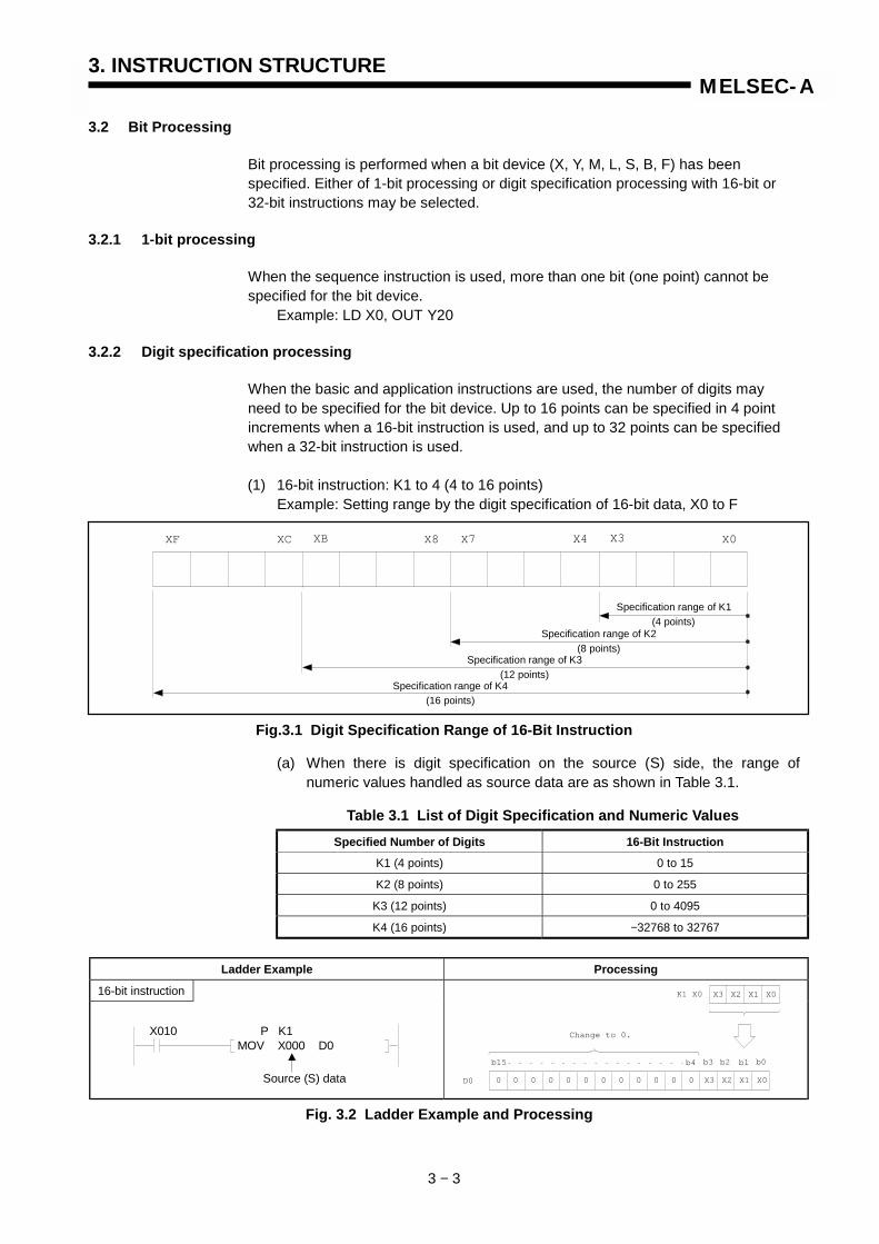
3. INSTRUCTION STRUCTURE
3 − 3
MELSEC-A
3.2 Bit Processing
Bit processing is performed when a bit device (X, Y, M, L, S, B, F) has beenspecified. Either of 1-bit processing or digit specification processing with 16-bit or32-bit instructions may be selected.
3.2.1 1-bit processing
When the sequence instruction is used, more than one bit (one point) cannot bespecified for the bit device.
Example: LD X0, OUT Y20
3.2.2 Digit specification processing
When the basic and application instructions are used, the number of digits mayneed to be specified for the bit device. Up to 16 points can be specified in 4 pointincrements when a 16-bit instruction is used, and up to 32 points can be specifiedwhen a 32-bit instruction is used.
(1) 16-bit instruction: K1 to 4 (4 to 16 points)Example: Setting range by the digit specification of 16-bit data, X0 to F
Fig.3.1 Digit Specification Range of 16-Bit Instruction
(a) When there is digit specification on the source (S) side, the range ofnumeric values handled as source data are as shown in Table 3.1.
Specified Number of Digits 16-Bit InstructionK1 (4 points) 0 to 15
K2 (8 points) 0 to 255
K3 (12 points) 0 to 4095
K4 (16 points) −32768 to 32767
Ladder Example Processing
16-bit instruction
XF XC XB X8 X7 X4 X3 X0
Specification range of K1(4 points)
Specification range of K2(8 points)
Specification range of K3(12 points)
Specification range of K4(16 points)
Table 3.1 List of Digit Specification and Numeric Values
D0
b3b4b15 b2 b1 b0
K1 X0
Change to 0.
0 0 0 0 0 0 0 0 0 0 0 0 X3 X2 X1 X0
X3 X2 X1 X0
Fig. 3.2 Ladder Example and Processing
Source (S) data
P K1MOV X000 D0
X010
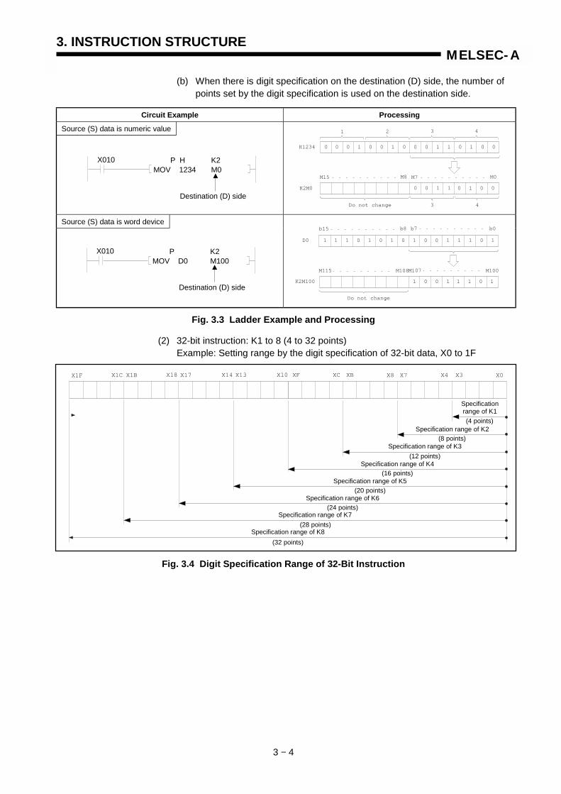
3. INSTRUCTION STRUCTURE
3 − 4
MELSEC-A
(b) When there is digit specification on the destination (D) side, the number ofpoints set by the digit specification is used on the destination side.
Circuit Example Processing
Source (S) data is numeric value
Source (S) data is word device
Fig. 3.3 Ladder Example and Processing
(2) 32-bit instruction: K1 to 8 (4 to 32 points)Example: Setting range by the digit specification of 32-bit data, X0 to 1F
Fig. 3.4 Digit Specification Range of 32-Bit Instruction
X1F X1C X1B X18 X17 X14 X13 X10 XC XBXF X8 X7 X4 X3 X0
Specificationrange of K1(4 points)
Specification range of K2(8 points)
Specification range of K3(12 points)
Specification range of K4(16 points)
Specification range of K5(20 points)
Specification range of K6(24 points)
Specification range of K7(28 points)
Specification range of K8(32 points)
K2M0
M15
Do not change.
1
H1234
M8 M7 M0
2 3 4
0 0 1 1
0 0 0 1 0 0 1 0 0 0 1 1
3 4
0 1 0 0
0 1 0 0
Destination (D) side
P HMOV 1234
X010 K2M0
K2M100
M115
Do not change.
D0
M108M107 M100
1 0 0 1
1 1 1 0 1 0 1 0 1 0 0 1 1 1 0 1
1 1 0 1
b15 b8 b7 b0
Destination (D) side
PMOV D0
X010 K2M100
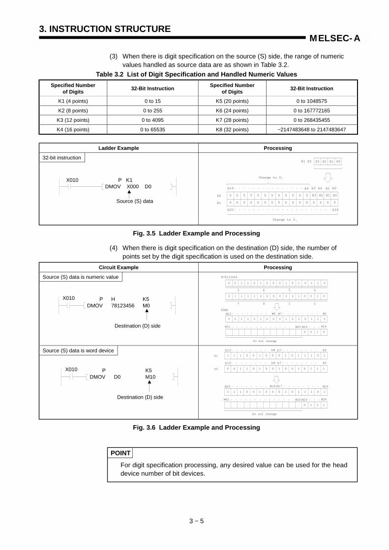
3. INSTRUCTION STRUCTURE
3 − 5
MELSEC-A
(3) When there is digit specification on the source (S) side, the range of numericvalues handled as source data are as shown in Table 3.2.
Table 3.2 List of Digit Specification and Handled Numeric ValuesSpecified Number
of Digits 32-Bit Instruction Specified Numberof Digits 32-Bit Instruction
K1 (4 points) 0 to 15 K5 (20 points) 0 to 1048575
K2 (8 points) 0 to 255 K6 (24 points) 0 to 167772165
K3 (12 points) 0 to 4095 K7 (28 points) 0 to 268435455
K4 (16 points) 0 to 65535 K8 (32 points) −2147483648 to 2147483647
Ladder Example Processing
32-bit instruction
Fig. 3.5 Ladder Example and Processing
(4) When there is digit specification on the destination (D) side, the number ofpoints set by the digit specification is used on the destination side.
Circuit Example Processing
Source (S) data is numeric value
Source (S) data is word device
Fig. 3.6 Ladder Example and Processing
POINT
For digit specification processing, any desired value can be used for the headdevice number of bit devices.
D0
b3b4b15 b2 b1 b0
K1 X0
Change to 0.
0 0 0 0 0 0 0 0 0 0 0 0 X3 X2 X1 X0
X3 X2 X1 X0
D1 0 0 0 0 0 0 0 0 0 0 0 0 0 0 0 0
b31 b16
Change to 0.
Source (S) data
P K1DMOV X000 D0
X010
0 0 0 1
0 0 1 1 0 1 0 0 0 1 0 1 0 1 1 0
0 0 1 0
Do not change.
0 0 1 1 0 1 0 0 0 1 0 1 0 1 1 0
0 0 1 0
M15 M8 M7 M0
M31 M20 M19 M16
3 4 5 6
7 8 1 2
H78123456
0 1 1 1 1 0 0 0
K5M0
Destination (D) side
X010 P H K5DMOV 78123456 M0
Do not change.
1 1 1 0 0 1 0 0 0 1 0 1 1 1 0 1
0 1 1 1
M25 M18 M17 M10
M41 M30 M29 M26
1 1 1 0 0 1 0 0 0 1 0 1 1 1 0 1
0 1 1 1
b15 b8 b7 b0
0 0 1 1 0 1 0 0 1 0 0 1
b15 b8 b7 b0
D1
D0
Destination (D) side
X010 P K5DMOV D0 M10

3. INSTRUCTION STRUCTURE
3 − 6
MELSEC-A
3.3 Handling of Numeric Values
In the A series, there are instructions which handle numeric values in 16 bits and 32bits.The highest bits of 16 bits and 32 bits are used for the judgement of positive andnegative. Therefore, numeric values handed by 16 bits and 32 bits are as follows:
POINTS
(1) Numeric value setting procedure
(a) Decimal
(b) Hexadecimal
(2) When FFFEH is divided by 2, the following occurs.
16 bits: -32768 to 3276732 bits: -2147483648 to 2147483647
10 is stored D10 in BIN value.
-10 is stored to D10 in BIN value.
10 is stored to D10 in hexadecimal.
32-bit instruction
Since FFFE is 65534, 65534/2=32767(7FFF) is stored to D0.
X010
X010
X010
MOVK10 D10
MOVK-10 D10
MOVH0010 D10
16-bit instruction
Since FFFE is -2,-2/2=-1 (FFFFH)is stored to D0.
X010D/
P H0000FFFE D0
K2
X010 P H K/ FFFE 2 D0
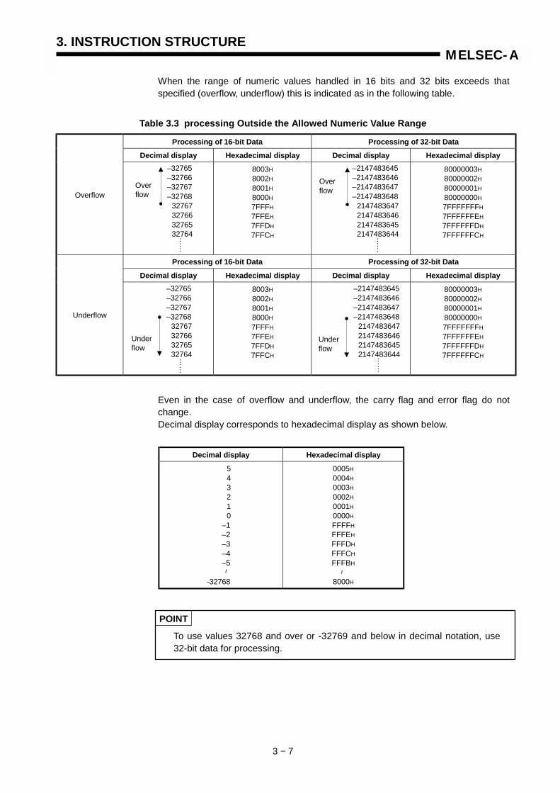
3. INSTRUCTION STRUCTURE
3 − 7
MELSEC-A
When the range of numeric values handled in 16 bits and 32 bits exceeds thatspecified (overflow, underflow) this is indicated as in the following table.
Table 3.3 processing Outside the Allowed Numeric Value Range
Processing of 16-bit Data Processing of 32-bit Data
Decimal display Hexadecimal display Decimal display Hexadecimal display
Overflow
8003H8002H
8001H8000H7FFFH
7FFEH7FFDH7FFCH
80000003H80000002H
80000001H80000000H7FFFFFFFH
7FFFFFFEH7FFFFFFDH7FFFFFFCH
Processing of 16-bit Data Processing of 32-bit Data
Decimal display Hexadecimal display Decimal display Hexadecimal display
Underflow
8003H
8002H8001H8000H
7FFFH7FFEH7FFDH7FFCH
80000003H
80000002H80000001H80000000H
7FFFFFFFH7FFFFFFEH7FFFFFFDH7FFFFFFCH
Even in the case of overflow and underflow, the carry flag and error flag do notchange.Decimal display corresponds to hexadecimal display as shown below.
Decimal display Hexadecimal display
543210
–1–2–3–4–5
-32768
0005H0004H0003H
0002H0001H0000H
FFFFHFFFEHFFFDH
FFFCHFFFBH
8000H
POINT
To use values 32768 and over or -32769 and below in decimal notation, use32-bit data for processing.
Overflow
–32765–32766–32767–32768
32767327663276532764
……
Overflow
–2147483645–2147483646–2147483647–2147483648
2147483647214748364621474836452147483644
Underflow
–32765–32766–32767–32768
32767327663276532764
Underflow
–2147483645–2147483646–2147483647–2147483648
2147483647214748364621474836452147483644
……
……
……
~ ~
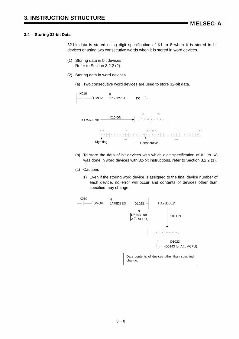
3. INSTRUCTION STRUCTURE
3 − 8
MELSEC-A
3.4 Storing 32-bit Data
32-bit data is stored using digit specification of K1 to 8 when it is stored in bitdevices or using two consecutive words when it is stored in word devices.
(1) Storing data in bit devicesRefer to Section 3.2.2 (2).
(2) Storing data in word devices
(a) Two consecutive word devices are used to store 32-bit data.
(b) To store the data of bit devices with which digit specification of K1 to K8was done in word devices with 32-bit instructions, refer to Section 3.2.2 (1).
(c) Cautions
1) Even if the storing word device is assigned to the final device number ofeach device, no error will occur and contents of devices other thanspecified may change.
X010DMOV
K175692781 D0
K175692781X10 ON
X010DMOV
H0A78DBED D1023 HA78DBED
D6143 forA ACPU
A 7 8 D B E D H
?
X10 ON
D1023(D6143 for A ACPU)
Data contents of devices other than specifiedchange.
b31 b16 b15 b0
D1 D0
0 0 0 0 1 0 1 0 0 1 1 1 1 0 0 0 1 1 0 1 1 0 1 1 1 1 1 0 1 1 0 1
to to
1 7 5 6 9 2 7 8 1
D1 D0
Sign flag Consecutive

3. INSTRUCTION STRUCTURE
3 − 9
MELSEC-A
2) Index registers can process 32-bit instructions when Z and V are usedin pairs. In this case, Z is regarded as the lower 16-bit device, andtherefore, V cannot be used in a 32-bit instruction. (Programs cannot beentered.)
If either of Z or V is specified for index qualification in the instruction,index qualification is performed regarding data in Z and V as 16-bit dataeven when 32-bit data is stored in Z and V.
REMARK
To handle 32-bit data with extension index registers Z1 to Z6 and V1 to V6 of AnA, A2AS, AnU,QCPU-A (A Mode) and A2USH board, refer to Section 3.8.5.
3) If one of two consecutive word devices used to store 32-bit data is usedin a 16-bit instruction, processing goes as follows.
X010DMOV
H0A78D8ED Z
V Z
A 7 8 D 8 E D H
HA78D8ED
X10 ON
X010DMOV
H12345678 Z
DMOV D2 D0Z
⋅⋅⋅⋅⋅⋅ Data 12345678H is stored in Z and V.
⋅⋅⋅⋅⋅⋅ Data in D0 and D1 become equal toD(2+5678H) and D(3+5678H), respectively.
X010DMOV
H0A78D8ED D0
MOV
MOV
D0
D1
D10
D11
⋅⋅⋅⋅⋅⋅• When D0 is specified:Data b0 to b15 of D0 and D1 are handled as D0 data.
⋅⋅⋅⋅⋅⋅• When D1 is specified:Data b16 to b31 of D0 and D1 are handled as D1 data.
b31 b16 b15 b0
D1 D0
0 0 0 0 1 0 1 0 0 1 1 1 1 0 0 0 1 1 0 1 1 0 1 1 1 1 1 0 1 1 0 1
to to
b31 b16
D11
0 0 0 0 1 0 1 0 0 1 1 1 1 0 0 0
to b15 b0
D10
1 1 0 1 1 0 1 1 1 1 1 0 1 1 0 1
to
D 8 E D HH
A 7 8 D 8 E D H
A 7 8
HA78D8EDX10 ON

3. INSTRUCTION STRUCTURE
3 − 10
MELSEC-A
3.5 Index Qualification
(1) The index qualification is used to specify the device number be providing anindex (Z, V) to the device and adding the specified device number and indexcontent.
(2) The index qualification can be used for devices X, Y, M, L, S, B, F, T, C, D, R,W, K, H, and P.
(3) The indexes (Z, V) are provided with a sign and can be set in the range of-32768 and 32767.
(4) The index qualification is as shown below.
Example:When the index qualification is performed, the actual processing devices are asshown below.(Z = 20, V = -5)
Ladder Example Actual Processing Device
X010MOV
HFFFF Z
X011MOV
ZD10 D0
FFFH (-1) is stored to Z.
Data of D10Z = D (10 +(-1)) = D9 is stored to D0.
Index qualification
X010
X011
MOVK20 Z
MOVK-5 V
MOVK Z100
VW053
X010
X011
MOVK20 Z
MOVK-5 V
MOVK2 ZX050
K1 VM38
X010
X011
MOVK20 Z
MOVK-5 V
MOVZ
D0K3 VY12F
X011MOV
K120 W04E
ExplanationK100Z …… K (100 + 20) = K120W53V …… W (53 - 5) = W4E
Hexadecimal
X011MOV
K2X064
K1M33
ExplanationK2X50Z…... K2X (50 + 14) = K2*64
K1M38 …… K1M (38 - 5) = K1M33K20 is converted into hexadecimal.
X011MOV D20
K3Y12A
ExplanationD0Z …… D (0 + 20) = D20K3Y12F …… K3Y (12F - 5) = K3Y12A
Hexadecimal
Fig. 3.7 Ladder Examples and Actual Devices Processed
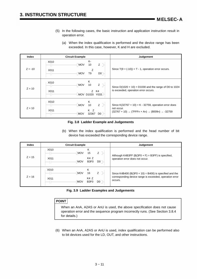
3. INSTRUCTION STRUCTURE
3 − 11
MELSEC-A
(5) In the following cases, the basic instruction and application instruction result inoperation error.
(a) When the index qualification is performed and the device range has beenexceeded. In this case, however, K and H are excluded.
Index Circuit Example Judgement
Z = -10 Since T(9 + (-10)) = T - 1, operation error occurs.
Z = 10 Since D(1020 + 10) = D1030 and the range of D0 to 1024is exceeded, operation error occurs.
Z = 10Since K(32767 + 10) = K - 32759, operation error doesnot occur.(32767 + 10) → (7FFFH + AH) → (8009H) → -32759
(b) When the index qualification is performed and the head number of bitdevice has exceeded the corresponding device range.
Index Circuit Example Judgement
Z = 15 Although K4B3FF (B(3F0 + F) = B3FF) is specified,operation error does not occur.
Z = 16Since K4B400 (B(3F0 + 10) = B400) is specified and thecorresponding device range is exceeded, operation erroroccurs.
POINT
When an AnA, A2AS or AnU is used, the above specification does not causeoperation error and the sequence program incorrectly runs. (See Section 3.8.4for details.)
(6) When an AnA, A2AS or AnU is used, index qualification can be performed alsoto bit devices used for the LD, OUT, and other instructions.
X010 K-MOV 10 Z
X011 ZMOV T9 D0
X010 KMOV 10 Z
X011 Z K4MOV D1020 Y033
X010 KMOV 10 Z
X011 K ZMOV 32367 D0
X010 KMOV 15 Z
X011 K4 ZMOV B3F0 D0
X010 KMOV 16 Z
X011 K4 ZMOV B3F0 D0
Fig. 3.8 Ladder Example and Judgements
Fig. 3.9 Ladder Examples and Judgements

3. INSTRUCTION STRUCTURE
3 − 12
MELSEC-A
3.6 Subset Processing
Subset processing is used to increase processing speed provided with the followingconditions when bit devices are specified in basic or application instructions.Instruction symbols are same as those of normal processings.
CPU Type Index Qualification Bit Device Word Device
AnAnNA3V, A2C, A52GA0J2H, AnS, AnSH,A1FXA73, A3N board
• Must not be used.
• Digit specificationmust be K4(16-bitprocessing)orK8(32-bit processing).
• The bit devicespecified must be amultiple of 8.
• No conditionprovided.
A3H, A3M • Must not be used.
• Digit specificationmust be K4(16-bitprocessing) orK8(32-bit processing).
• The bit devicespecified must be amultiple of 16.
• File register (R) mustnot be used.
AnA, A2AS, AnU • Must not be used tobit devices.
• Digit specificationmust be K4(16-bitprocessing) or K8(32-bit processing).
• The bit devicespecified must be amultiple of 16.
• File register (R) andindex registers(Z and V) must notbe used.
3.7 Operation Error
(1) In the following cases, the basic instruction and application instruction result inoperation error.
(a) Error described in the explanation of each instruction has occurred.
(b) When the result of index qualification includes error.(See Section 3.5 (5).)
POINT
If the specified range of a device has exceeded the allowable device range,data will be written to devices other than the specified one without causing anoperation error. Therefore, caution shuld be exercised.
Z and V areexcluded whenindex qualificationis performed toword devices.
Table 3.4 Conditions for Subset Processing
Although B3F8 to 407 have beenspecified, B400 to 407 do not exist.
Although W3FF and 400 have beenspecified, W400 does not existactually.
X010MOV DO B3F8
K4
X010DMOV DO W3FF
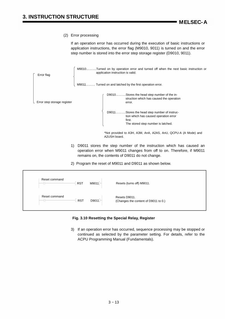
3. INSTRUCTION STRUCTURE
3 − 13
MELSEC-A
(2) Error processing
If an operation error has occurred during the execution of basic instructions orapplication instructions, the error flag (M9010, 9011) is turned on and the errorstep number is stored into the error step storage register (D9010, 9011).
1) D9011 stores the step number of the instruction which has caused anoperation error when M9011 changes from off to on. Therefore, if M9011remains on, the contents of D9011 do not change.
2) Program the reset of M9011 and D9011 as shown below.
Fig. 3.10 Resetting the Special Relay, Register
3) If an operation error has occurred, sequence processing may be stopped orcontinued as selected by the parameter setting. For details, refer to theACPU Programming Manual (Fundamentals).
Error flag
*Not provided to A3H, A3M, AnA, A2AS, AnU, QCPU-A (A Mode) andA2USH board.
M9010……….Turned on by operation error and turned off when the next basic instruction orapplication instruction is valid.
M9011……… Turned on and latched by the first operation error.
D9010……….Stores the head step number of the in-struction which has caused the operationerror.
D9011……….Stores the head step number of instruc-tion which has caused operation errorfirst.The stored step number is latched.
Error step storage register
Resets (turns off) M9011.
Resets D9011.(Changes the content of D9011 to 0.)
Reset command
Reset command
RST M9011
RST D9011
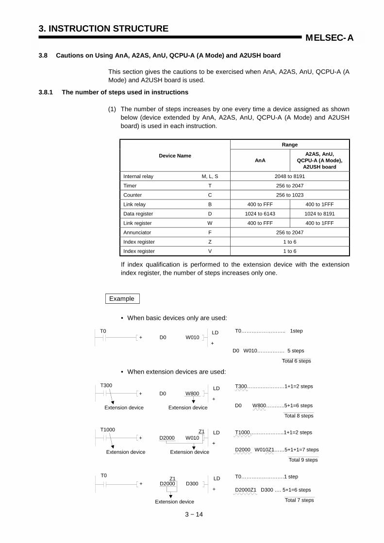
3. INSTRUCTION STRUCTURE
3 − 14
MELSEC-A
3.8 Cautions on Using AnA, A2AS, AnU, QCPU-A (A Mode) and A2USH board
This section gives the cautions to be exercised when AnA, A2AS, AnU, QCPU-A (AMode) and A2USH board is used.
3.8.1 The number of steps used in instructions
(1) The number of steps increases by one every time a device assigned as shownbelow (device extended by AnA, A2AS, AnU, QCPU-A (A Mode) and A2USHboard) is used in each instruction.
Range
Device NameAnA
A2AS, AnU,QCPU-A (A Mode),
A2USH board
Internal relay M, L, S 2048 to 8191
Timer T 256 to 2047
Counter C 256 to 1023
Link relay B 400 to FFF 400 to 1FFF
Data register D 1024 to 6143 1024 to 8191
Link register W 400 to FFF 400 to 1FFF
Annunciator F 256 to 2047
Index register Z 1 to 6
Index register V 1 to 6
If index qualification is performed to the extension device with the extensionindex register, the number of steps increases only one.
Example
• When basic devices only are used:
• When extension devices are used:
D0 W010……………. 5 steps
Total 6 steps
T0…………………….. 1stepT0+ D0 W010
LD
+
T300……….…………1+1=2 steps
D0 W800………..5+1=6 steps
Total 8 steps
D2000Z1 D300 …. 5+1=6 steps
Total 7 steps
Extension device Extension device
T300+ D0 W800
LD
+
T1000………………..1+1=2 steps
D2000 W010Z1……5+1+1=7 steps
Total 9 steps
Extension device
T0…………………….1 step
Extension device Extension device
T1000+ D2000 W010
LD
+
Z1
T0+ D2000 D300
LD
+
Z1
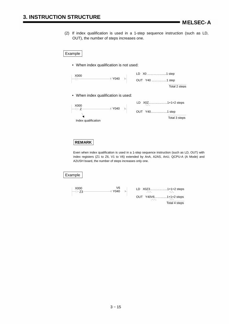
3. INSTRUCTION STRUCTURE
3 − 15
MELSEC-A
(2) If index qualification is used in a 1-step sequence instruction (such as LD,OUT), the number of steps increases one.
Example
• When index qualification is not used:
• When index qualification is used:
REMARK
Even when index qualification is used in a 1-step sequence instruction (such as LD, OUT) withindex registers (Z1 to Z6, V1 to V6) extended by AnA, A2AS, AnU, QCPU-A (A Mode) andA2USH board, the number of steps increases only one.
Example
LD X0 ……………....1 step
OUT Y40 ……….…..1 step
Total 2 steps
LD X0Z………………1+1=2 steps
OUT Y40…………….1 step
Total 3 stepsIndex qualification
( )X000
Y040
LD X0Z3……………..1+1=2 steps
OUT Y40V6…………1+1=2 steps
Total 4 steps
( )X000
Y040V6
( )X000
Y040Z
Z3
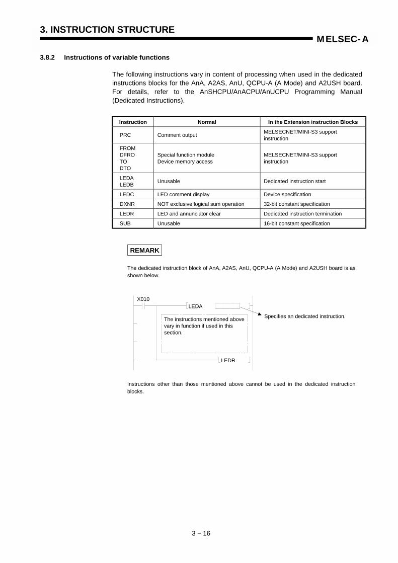
3. INSTRUCTION STRUCTURE
3 − 16
MELSEC-A
3.8.2 Instructions of variable functions
The following instructions vary in content of processing when used in the dedicatedinstructions blocks for the AnA, A2AS, AnU, QCPU-A (A Mode) and A2USH board.For details, refer to the AnSHCPU/AnACPU/AnUCPU Programming Manual(Dedicated Instructions).
Instruction Normal In the Extension instruction Blocks
PRC Comment output MELSECNET/MINI-S3 supportinstruction
FROMDFROTODTO
Special function moduleDevice memory access
MELSECNET/MINI-S3 supportinstruction
LEDALEDB Unusable Dedicated instruction start
LEDC LED comment display Device specification
DXNR NOT exclusive logical sum operation 32-bit constant specification
LEDR LED and annunciator clear Dedicated instruction termination
SUB Unusable 16-bit constant specification
REMARK
The dedicated instruction block of AnA, A2AS, AnU, QCPU-A (A Mode) and A2USH board is asshown below.
Instructions other than those mentioned above cannot be used in the dedicated instructionblocks.
X010LEDA
LEDR
The instructions mentioned abovevary in function if used in thissection.
Specifies an dedicated instruction.
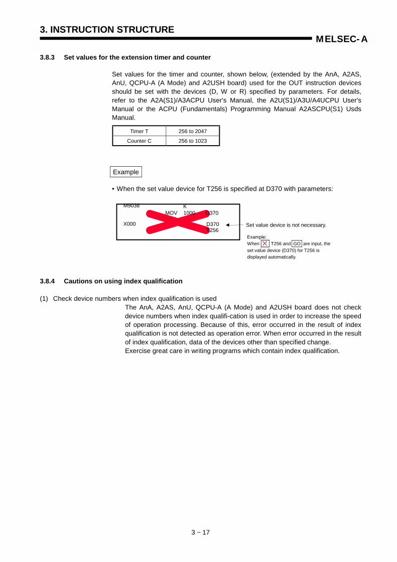
3. INSTRUCTION STRUCTURE
3 − 17
MELSEC-A
3.8.3 Set values for the extension timer and counter
Set values for the timer and counter, shown below, (extended by the AnA, A2AS,AnU, QCPU-A (A Mode) and A2USH board) used for the OUT instruction devicesshould be set with the devices (D, W or R) specified by parameters. For details,refer to the A2A(S1)/A3ACPU User's Manual, the A2U(S1)/A3U/A4UCPU User'sManual or the ACPU (Fundamentals) Programming Manual A2ASCPU(S1) UsdsManual.
Timer T 256 to 2047
Counter C 256 to 1023
Example
• When the set value device for T256 is specified at D370 with parameters:
3.8.4 Cautions on using index qualification
(1) Check device numbers when index qualification is usedThe AnA, A2AS, AnU, QCPU-A (A Mode) and A2USH board does not checkdevice numbers when index qualifi-cation is used in order to increase the speedof operation processing. Because of this, error occurred in the result of indexqualification is not detected as operation error. When error occurred in the resultof index qualification, data of the devices other than specified change.Exercise great care in writing programs which contain index qualification.
M9038 KMOV 1000 D370
D370T256
Set value device is not necessary.X000
Example:When T256 and GO are input, theset value device (D370) for T256 isdisplayed automatically.

3. INSTRUCTION STRUCTURE
3 − 18
MELSEC-A
(2) Turn-on/off instruction operations at index qualificationWhen the turn-on/off instructions (PLS, PLF, SETF , RSTF , P) aredesignated with index qualification when an AnA, A2AS, AnU, QCPU-A (AMode) or A2USH board is used, the instructions are executed only when theexecution condition for the turn-on/off execution instruction is established.
Example 1
When M1, M2 and M4 are ON, and M3 is OFF in the circuit shown below:
M1Z SET F1Z F1ZNumber of
scans Device No. ON/OFF state Executioncondition
Execution/noexecution state Device No. ON/OFF state
1st scan M1 ON *2 *2 F1 *2
2nd scan M2 ON ON → ON(not established) No execution F2 OFF
3rd scan M3 OFF ON → OFF(not established) No execution F3 OFF
4th scan M4 ON OFF → ON(established) Execution F4 ON
Example 2
1Z goes On when M1Z goes On.Operation in the case where M1, M2 and M4 are On, and M3 is Off in the circuit inthe following figure.
Cautions when a PLS instruction with Index / Startup execution instruction is used ina FOR-NEXT.When a device which functions as a conditions for execution of the PLS instruction /Startup execution command starts up, the PLS command / Startup executioninstruction is executed.
M1ZSET F1Z
INC ZM9036
RST Z=K4 Z
M9036
M1Z
RST Z
FOR K4
Z is cleared.
SET F1Z Execution/no execution ofSETF (1 + Z)
INC Z Z + 1 is executed.
NEXT
*1
M9036

3. INSTRUCTION STRUCTURE
3 − 19
MELSEC-A
M1Z SET F1Z F1ZFOR instruction
Device No. ON/OFF state Executioncondition
Execution/noexecution state Device No. ON/OFF state
1st M1 ON *2 *2 F1 *2
2nd M2 ON ON → ON(not established) No execution F2 OFF
3rd M3 OFF ON → OFF(not established) No execution F3 OFF
4th M4 ON OFF → ON(established) Execution F4 ON
REMARKS
1) *1: Execution/no execution is determined by comparing the device states between thepresent states and that of one scan before/previous time.
Present device Device of one scan before/previous timeM1 M4M2 M1M3 M2M4 M3
2) *2: Varies according to the M4 ON/OFF state of one scan before.
SET F1Z F1ZM4 state of one
scan before Executioncondition
Execution/noexecution state Device No. ON/OFF state
OFF OFF → ON(established) Execution ON
ON ON → ON(not established) No execution
F1OFF
3) *3: Device state changes in the order of M1, M2, M3 and M4 in 4 scans, and returns to M1 in the 5th scan.
*1
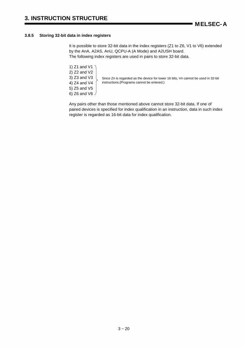
3. INSTRUCTION STRUCTURE
3 − 20
MELSEC-A
3.8.5 Storing 32-bit data in index registers
It is possible to store 32-bit data in the index registers (Z1 to Z6, V1 to V6) extendedby the AnA, A2AS, AnU, QCPU-A (A Mode) and A2USH board.The following index registers are used in pairs to store 32-bit data.
1) Z1 and V12) Z2 and V23) Z3 and V34) Z4 and V45) Z5 and V56) Z6 and V6
Any pairs other than those mentioned above cannot store 32-bit data. If one ofpaired devices is specified for index qualification in an instruction, data in such indexregister is regarded as 16-bit data for index qualification.
Since Zn is regarded as the device for lower 16 bits, Vn cannot be used in 32-bitinstructions.(Programs cannot be entered.)
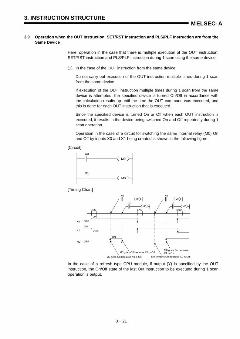
3. INSTRUCTION STRUCTURE
3 − 21
MELSEC-A
3.9 Operation when the OUT Instruction, SET/RST Instruction and PLS/PLF Instruction are from theSame Device
Here, operation in the case that there is multiple execution of the OUT instruction,SET/RST instruction and PLS/PLF instruction during 1 scan using the same device.
(1) In the case of the OUT instruction from the same device.
Do not carry out execution of the OUT instruction multiple times during 1 scanfrom the same device.
If execution of the OUT instruction multiple times during 1 scan from the samedevice is attempted, the specified device is turned On/Off in accordance withthe calculation results up until the time the OUT command was executed, andthis is done for each OUT instruction that is executed.
Since the specified device is turned On or Off when each OUT instruction isexecuted, it results in the device being switched On and Off repeatedly during 1scan operation.
Operation in the case of a circuit for switching the same internal relay (M0) Onand Off by inputs X0 and X1 being created is shown in the following figure.
[Circuit]
M0X0
M0X1
[Timing Chart]
M0
M0
M0
M0
M0 goes On because X0 is On.
M0 goes Off because X1 is Off.
M0 remains Off because X0 is Off.
M0 goes On because X1 is On.
OFF
ON
ON
OFF
ON
END END END
X0
X1
M0
X0 X0
X1 X1
OFF
In the case of a refresh type CPU module, if output (Y) is specified by the OUTinstruction, the On/Off state of the last Out instruction to be executed during 1 scanoperation is output.
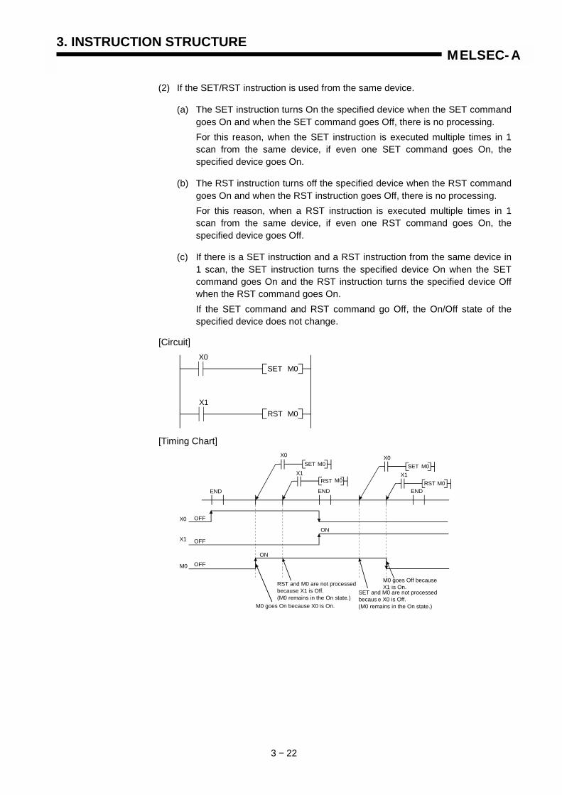
3. INSTRUCTION STRUCTURE
3 − 22
MELSEC-A
(2) If the SET/RST instruction is used from the same device.
(a) The SET instruction turns On the specified device when the SET commandgoes On and when the SET command goes Off, there is no processing.For this reason, when the SET instruction is executed multiple times in 1scan from the same device, if even one SET command goes On, thespecified device goes On.
(b) The RST instruction turns off the specified device when the RST commandgoes On and when the RST instruction goes Off, there is no processing.For this reason, when a RST instruction is executed multiple times in 1scan from the same device, if even one RST command goes On, thespecified device goes Off.
(c) If there is a SET instruction and a RST instruction from the same device in1 scan, the SET instruction turns the specified device On when the SETcommand goes On and the RST instruction turns the specified device Offwhen the RST command goes On.If the SET command and RST command go Off, the On/Off state of thespecified device does not change.
[Circuit]
M0X0
X1
SET
M0RST
[Timing Chart]
M0
M0 goes On because X0 is On.
RST and M0 are not processedbecause X1 is Off.(M0 remains in the On state.)
SET and M0 are not processedbecaus e X0 is Off.(M0 remains in the On state.)
M0 goes Off becauseX1 is On.
OFF
ON
END END END
X0
X1
M0
OFF
OFF
ON
SETX0
X1M0RST
M0SET
M0RST
X0
X1
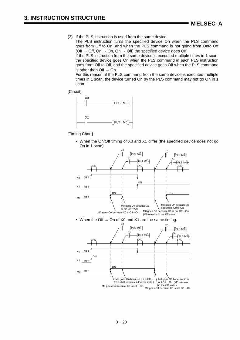
3. INSTRUCTION STRUCTURE
3 − 23
MELSEC-A
(3) If the PLS instruction is used from the same device.The PLS instruction turns the specified device On when the PLS commandgoes from Off to On, and when the PLS command is not going from Onto Off(Off → Off, On → On, On → Off) the specified device goes Off.If the PLS instruction from the same device is executed multiple times in 1 scan,the specified device goes On when the PLS command in each PLS instructiongoes from Off to Off, and the specified device goes Off when the PLS commandis other than Off → On.For this reason, if the PLS command from the same device is executed multipletimes in 1 scan, the device turned On by the PLS command may not go On in 1scan.
[Circuit]
M0X0
X1
PLS
M0PLS
[Timing Chart]
• When the On/Off timing of X0 and X1 differ (the specified device does not goOn in 1 scan)
M0
M0 goes On because X1 goes from Off to On.
OFF
ON
END END END
X0
X1
M0
OFF
OFF
ON
PLSX0
X1M0PLS
M0PLS
M0PLS
X0
X1
ON
M0 goes Off because X0 is not Off On. (M0 remains in the Off state.)
M0 goes Off because X1 is not Off On.
M0 goes On because X0 is Off On.
• When the Off → On of X0 and X1 are the same timing.
M0
OFF
ON
END END END
X0
X1
M0
OFF
OFF
ON
PLSX0
X1M0PLS
M0PLS
M0PLS
X0
X1
M0 goes On because X1 is Off On. (M0 remains in the On state.)
M0 goes On because X0 is Off On.
M0 goes Off because X1 is not Off On. (M0 remains in the Off state.)
M0 goes Off because X0 is not Off On.
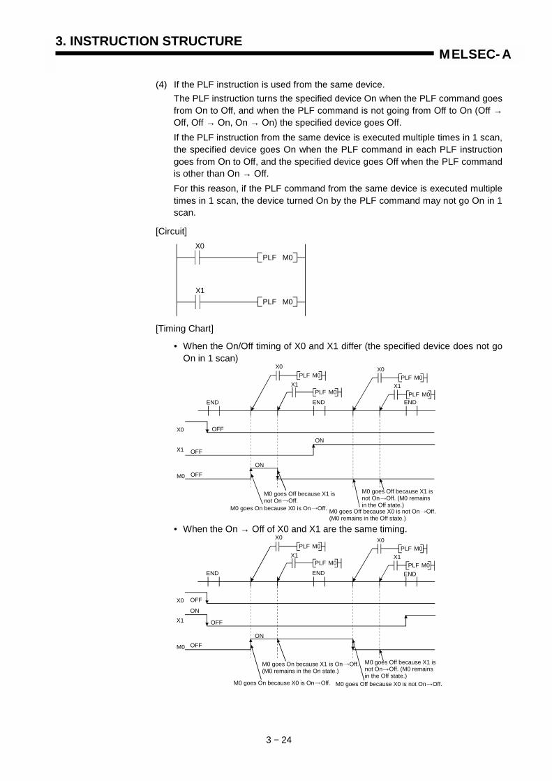
3. INSTRUCTION STRUCTURE
3 − 24
MELSEC-A
(4) If the PLF instruction is used from the same device.The PLF instruction turns the specified device On when the PLF command goesfrom On to Off, and when the PLF command is not going from Off to On (Off →Off, Off → On, On → On) the specified device goes Off.If the PLF instruction from the same device is executed multiple times in 1 scan,the specified device goes On when the PLF command in each PLF instructiongoes from On to Off, and the specified device goes Off when the PLF commandis other than On → Off.For this reason, if the PLF command from the same device is executed multipletimes in 1 scan, the device turned On by the PLF command may not go On in 1scan.
[Circuit]
M0X0
X1
PLF
M0PLF
[Timing Chart]
• When the On/Off timing of X0 and X1 differ (the specified device does not goOn in 1 scan)
M0
OFF
ON
END END END
X0
X1
M0
OFF
OFF
ON
PLFX0
X1M0PLF
M0PLF
M0PLF
X0
X1
M0 goes Off because X0 is not On Off. (M0 remains in the Off state.)
M0 goes Off because X1 is not On Off. (M0 remains in the Off state.)M0 goes On because X0 is On Off.
M0 goes Off because X1 is not On Off.
• When the On → Off of X0 and X1 are the same timing.
M0
OFF
ON
END END END
X0
X1
M0
OFF
OFF
PLFX0
X1M0PLF
M0PLF
M0PLF
X0
X1
ON
M0 goes Off because X0 is not On Off.
M0 goes Off because X1 is not On Off. (M0 remains in the Off state.)
M0 goes On because X0 is On Off.
M0 goes On because X1 is On Off. (M0 remains in the On state.)
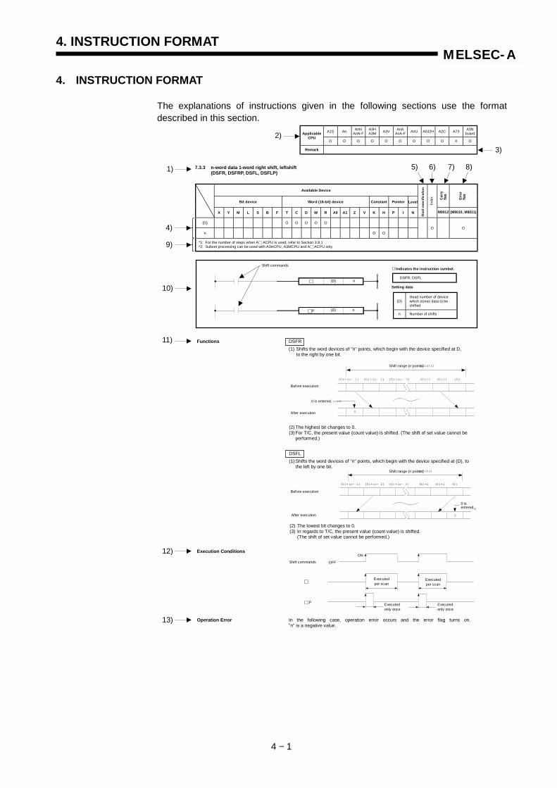
4. INSTRUCTION FORMAT
4 − 1
MELSEC-A
4. INSTRUCTION FORMAT
The explanations of instructions given in the following sections use the formatdescribed in this section.
Available Device
Bit device Word (16-bit) device Constant Pointer Level
X Y M L S B F T C D W R A0 A1 Z V K H P I N M9012 (M9010, M9011)
(D) O O O O O
n O OO O
*1: For the number of steps when A ACPU is used, refer to Section 3.8.1*2: Subset processing can be used with A3HCPU, A3MCPU and A ACPU only
A1S An AnNAnN-F
A3HA3M A3V AnA
AnA-F AnU A0J2H A2C A73 A3NboardApplicable
CPUO O O O O O O O O X O
Remark
7.3.3 n-word data 1-word right shift, leftshift (DSFR, DSFRP, DSFL, DSFLP)
(D)Head number of devicewhich stores data to beshifted
n Number of shifts
Setting data
DSFR, DSFL
Indicates the instruction symbol.Shift commands
(D) n
(D) nP
Digi
tspe
cific
atio
n
Functions DSFR(1) Shifts the word devices of "n" points, which begin with the device specified at D,
to the right by one bit.
(2) The highest bit changes to 0.(3) For T/C, the present value (count value) is shifted. (The shift of set value cannot be
performed.)
DSFL(1) Shifts the word devices of "n" points, which begin with the device specified at (D), to
the left by one bit.
(2) The lowest bit changes to 0.(3) In regards to T/C, the present value (count value) is shifted.
(The shift of set value cannot be performed.)
Execution Conditions
OFF
ON
Executedper scan
Executedonly once
P
Shift commands
Executedper scan
Executedonly once
Operation Error In the following case, operation error occurs and the error flag turns on."n" is a negative value.
2)
3)
1)
4)
9)
10)
11)
12)
13)
Carry
flag
Erro
rfla
g
8)7)6)5)
0
(D)+(n- 1) (D)+(n- 2) (D)+(n- 3) (D)+2 (D)+1 (D)
Shift range (n points)
0 is entered.
Before execution
After execution
Shift range (n points)
0 is entered.
(D)+(n- 1) (D)+(n- 2) (D)+(n- 3) (D)+2 (D)+1 (D)
Shift range (n points)
0
0 is entered
Before execution
After execution
Shift range (n points)
0 isentered.
Inde
x

4. INSTRUCTION FORMAT
4 − 2
MELSEC-A
0XB
DSFLP D683 K7
Program Examples DSFRProgram which shifts the contents of D683 to 689 to the right when XB turns on.
• Coding0 LD XB1 DSFRP D683 K78 END
Specification range of DSFRP instruction
0
D688D689 D687 D686 D685 D684 D683
-100 503 600 -336 3802 -32765 5003
0 -100 503 600 -336 3802 -32765
Before execution
After execution
Specification range of DSFRP instruction
DSFLProgram which shifts the contents of D683 to 689 to the left when XB turns on.
• Coding0 LD XB1 DSFLP D683 K78 END
Specification range of DSFRP instruction
0
D688D689 D687 D686 D685 D684 D683
-100 503 600 -336 3802 -32765 5003
503 600 -336 3802 -32765 5003 0
Before execution
After execution
Specification range of DSFRP instruction
14)
0XB
DSFRP D683 K7
4. INSTRUCTION FORMAT
4 − 3
MELSEC-A
Explanations
(1) Indicates section number, and title and symbol of instruction.
(2) Indicates usable CPUs.O : Usable : Usable with some CPUs or needs special operations for use.X : Unusable
If the instruction is usable with all types of CPUs, it is indicated as follows.
ApplicableCPU All CPUs
(3) Describes details of 2). Pay special attention if the mark is given.
(4) Circles are given to devices which can be used for instructions.
(5) Indicates digits which can be specified when the bit device requires digitspecification.
(6) A circle (O) is given to the instruction which can use index qualification (Z or Vis added). A triangle ( ) is given to the instruction which can use indexqualification with some specific types of CPUs.
(7) A circle (O) is given to the instruction which can turn the carry flag ON.
(8) A circle (O) is given to the instruction which can turn the error flag ON whenoperation error occurs.
(9) Gives notes concerning (4) to (10) above. Pay special attention if the O or mark is given.
(10) Indicates the format of instructions in ladder mode.
(11) Described the instruction.
(12) Indicates the execution conditions of instructions.
(13) Indicates conditions which result in operation error.
(14) Describes program examples in ladder mode and list mode.
REMARK
Program display in list mode is as follows.
For the input procedure of the program, refer to the Operating Manual of respective peripheraldevice.
0 LD M90361 DBIN K6X020 D9
10 D* D9 K10000 D521 BIN K4X010 D326 MOV K0 D431 D+ D3 D5 D042 END
Step No. Instruction Devices
∗
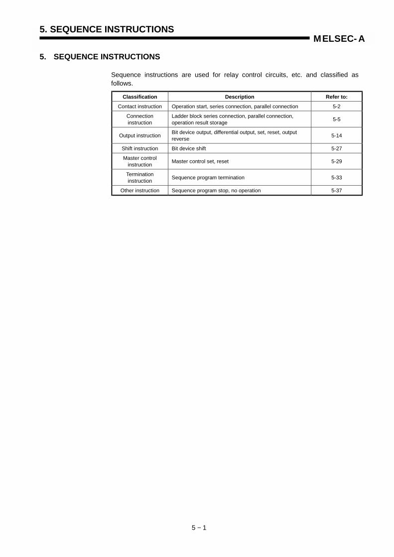
5. SEQUENCE INSTRUCTIONS
5 − 1
MELSEC-A
5. SEQUENCE INSTRUCTIONS
Sequence instructions are used for relay control circuits, etc. and classified asfollows.
Classification Description Refer to:
Contact instruction Operation start, series connection, parallel connection 5-2
Connectioninstruction
Ladder block series connection, parallel connection,operation result storage 5-5
Output instruction Bit device output, differential output, set, reset, outputreverse 5-14
Shift instruction Bit device shift 5-27
Master controlinstruction Master control set, reset 5-29
Terminationinstruction Sequence program termination 5-33
Other instruction Sequence program stop, no operation 5-37

5. SEQUENCE INSTRUCTIONS
5 − 2
MELSEC-A
5.1 Contact Instructions
5.1.1 Operation start, series connection,parallel connection(LD, LDI, AND, ANI, OR, ORI)
Available Device
Bit device Word (16-bit) device Constant Pointer Level Car
ryfla
g
Erro
rfla
g
X Y M L S B F T C D W R A0 A1 Z V K H P I N
Digi
t spe
cific
atio
n
Inde
x
M9012 (M9010, M9011)
O O O O O O O O O
*1: Index qualification can be used with AnA, A2AS, AnU, QCPU-A (A Mode) and A2USH board only.
Functions LD,LDI(1) LD is the contact A operation start instruction and LDI is the contact B operation
start instruction. They draw the ON/OFF data of the specified device and usethe data as an operation result.
AND,ANI(1) AND is the NO contact series connection instruction and ANI is the NC contact
series connection instruction. They read the ON/OFF data of the specifieddevice, performs the AND operation of that data and the previous operationresult, and use it as a new operation result.
(2) There are no restrictions on the use of AND and ANI. However, the followingconditions are provided in ladder mode on the GPP.
1) Write: When AND or ANI is connected serially, a circuit of up to 21 stages can be written.
2) Read: When AND or ANI is connected serially, a circuit of up to 24 stages can be displayed at one time. if a circuit has 25 or more stages, stages 1to 24 are displayed at one time.
ApplicableCPU All CPUs
LD
LDI
AND
ANI
OR
ORI
X001
X003
X001
X002
X002
X003
Device number
*1
5. SEQUENCE INSTRUCTIONS
5 − 3
MELSEC-A
OR, ORI(1) OR is the parallel connection instruction of one contact A and ORI is the parallel
connection instruction of one contact B. They draw the ON/OFF data of thespecified device, performs the OR operation of that data and the previousoperation result, and use it as a new operation result.
(2) There are no restrictions on the use of OR and ORI. However, the followingconditions are provided in ladder mode on the GPP.
1) Write: A circuit, in which up to 23 ORs or ORIs are connected consecutively, may be written.
2) Read: A circuit, in which up to 23 ORs or ORIs are connected consecutively, may be displayed. A circuit containing more than 23 ORs or ORIs cannot be completely displayed.
Execution Executed every scan independently of the device status and operation result.Conditions

5. SEQUENCE INSTRUCTIONS
5 − 4
MELSEC-A
Program Examples LD , LD2 , AND , ANI , OR , ORI
• Coding0 LD X0031 OR X0042 OR X0053 OUT Y0334 LD X0055 AND M116 ORI X0067 OUT Y0348 END
( )
( )X003
X004
X005
X005
X006
M11
Y033
Y034
0
4
•••• Coding0 LD X0031 AND M62 LDI X0043 ANI X0074 ORB5 ANI M96 OUT Y0337 LD X0058 LD M89 OR M9
10 ANB11 ANI M1112 OUT Y03413 END
( )
( )
X003
X004
X005
M6
X007
M8
M9
M9
M11
Y033
Y034
0
7
ANB
ORB
•••• Coding0 LD X0051 OUT Y0352 AND X0083 OUT Y0364 ANI X0095 OUT Y0376 END
( )
( )
( )
X005
X008
X009
Y035
Y036
Y037
0

MEMO
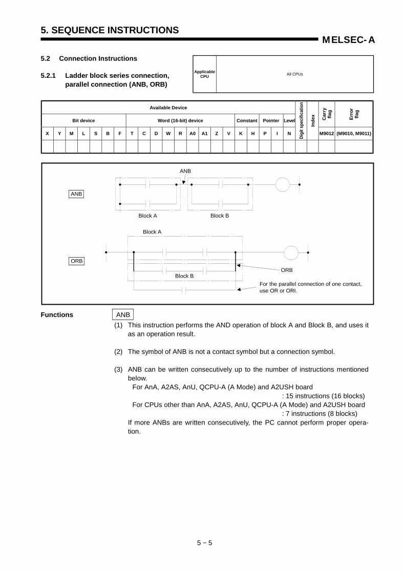
5. SEQUENCE INSTRUCTIONS
5 − 5
MELSEC-A
5.2 Connection Instructions
5.2.1 Ladder block series connection,parallel connection (ANB, ORB)
Available Device
Bit device Word (16-bit) device Constant Pointer Level Car
ryfla
g
Erro
rfla
g
X Y M L S B F T C D W R A0 A1 Z V K H P I N
Digi
t spe
cific
atio
n
Inde
x
M9012 (M9010, M9011)
Functions ANB(1) This instruction performs the AND operation of block A and Block B, and uses it
as an operation result.
(2) The symbol of ANB is not a contact symbol but a connection symbol.
(3) ANB can be written consecutively up to the number of instructions mentionedbelow.
For AnA, A2AS, AnU, QCPU-A (A Mode) and A2USH board: 15 instructions (16 blocks)
For CPUs other than AnA, A2AS, AnU, QCPU-A (A Mode) and A2USH board: 7 instructions (8 blocks)
If more ANBs are written consecutively, the PC cannot perform proper opera-tion.
ApplicableCPU All CPUs
ANB
Block A Block B
ORB
Block A
Block BFor the parallel connection of one contact,use OR or ORI.
ANB
ORB

5. SEQUENCE INSTRUCTIONS
5 − 6
MELSEC-A
ORB(1) This instruction performs the OR operation of block A and block B, and uses it
as an operation result.
(2) ORB performs parallel connection of circuit blocks with two or more contacts.For parallel connection of circuit blocks which have only one contact, OR andORI are used and ORB is not required. (See below.)
(3) The symbol of ORB is not a contact symbol but a connection symbol.
(4) ORB can be written consecutively up to the number of instructions mentionedbelow.
For AnA, A2AS, AnU, QCPU-A (A Mode) and A2USH board: 15 instructions (16 blocks)
For CPUs other than AnA, A2AS, AnU, QCPU-A (A Mode) and A2USH board: 7 instructions (8 blocks)
If more ORBs are written consecutively, the PC cannot perform proper opera-tion.
( )
•••• Coding0 LD X0001 AND X0012 LD X0023 AND X0034 ORB5 OR X0046 OUT Y0107 END
X001X000
X003X002
Y010
X004
0

5. SEQUENCE INSTRUCTIONS
5 − 7
MELSEC-A
Program Examples ANBWhen circuit blocks are serially connected consecutively, the coding of program isavailable in two types. However, proceed with the coding according to Codingexample 1.
( )X002X000
X003X001
0X006X004
X007X005
X008
X009
M7
•••• Coding example 10 LD X0001 OR X0012 LD X0023 OR X0034 ANB5 LD X0046 OR X0057 ANB8 LD X0069 OR X007
10 ANB11 LD X00812 OR X00913 ANB14 OUT M715 END
•••• Coding example 20 LD X0001 OR X0012 LD X0023 OR X0034 LD X0045 OR X0056 LD X0067 OR X0078 LD X0089 OR X009
10 ANB11 ANB12 ANB13 ANB14 OUT M715 END
There is no restriction on the number of ANBsused.
If ANBs are written consecutively exceeding thenumber mentioned below, the PC cannot per-form proper operation.For AnA, A2AS, AnU, QCPU-A (A Mode) andA2USH board: 15 instructions
(16 blocks)For CPUs other than AnA, A2AS, AnU, QCPU-A(A Mode) and A2USH board: 7 instructions
(8 blocks)
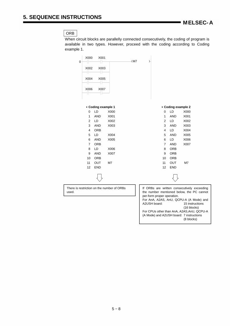
5. SEQUENCE INSTRUCTIONS
5 − 8
MELSEC-A
ORBWhen circuit blocks are parallelly connected consecutively, the coding of program isavailable in two types. However, proceed with the coding according to Codingexample 1.
( )X001X000
X003X002
M70
X005X004
X007X006
•••• Coding example 10 LD X0001 AND X0012 LD X0023 AND X0034 ORB5 LD X0046 AND X0057 ORB8 LD X0069 AND X007
10 ORB11 OUT M712 END
•••• Coding example 20 LD X0001 AND X0012 LD X0023 AND X0034 LD X0045 AND X0056 LD X0067 AND X0078 ORB9 ORB
10 ORB11 OUT M712 END
There is restriction on the number of ORBsused.
If ORBs are written consecutively exceedingthe number mentioned below, the PC cannotper-form proper operation.For AnA, A2AS, AnU, QCPU-A (A Mode) andA2USH board: 15 instructions
(16 blocks)For CPUs other than AnA, A2AS,AnU, QCPU-A(A Mode) and A2USH board: 7 instructions
(8 blocks)

5. SEQUENCE INSTRUCTIONS
5 − 9
MELSEC-A
5.2.2 Operation result push, read, pop(MPS, MRD, MPP)
Available Device
Bit device Word (16-bit) device Constant Pointer Level Car
ryfla
g
Erro
rfla
g
X Y M L S B F T C D W R A0 A1 Z V K H P I N
Digi
t spe
cific
atio
n
Inde
x
M9012 (M9010, M9011)
Functions MPS(1) Stores the operation result (ON/OFF) immediately preceding the MPS instruc-
tion.
(2) The MPS instruction can be used up to the number of times mentioned below.For AnA, A2AS, AnU, QCPU-A (A Mode) and A2USH board : 16 timesFor CPUs other than AnA, A2AS, AnU, QCPU-A (A Mode) and A2USH board
: 12 timesHowever, it can be used 11 times consecutively in ladder mode. If an MPPinstruction is used in between, 1 is reduced from the number of used MPSinstructions.
MRD(1) Reads the operation result stored by the MPS instruction, and resumes the
operation with that operation result, starting at the next step.
ApplicableCPU All CPUs
MPS
MRD
MPP
When the ladder is dispiayed, MPS, MRD, and MPPare omitted.

5. SEQUENCE INSTRUCTIONS
5 − 10
MELSEC-A
MPP(1) Reads the operation result stored by the MPS instruction, and resumes the
operation with that operation result, starting at the next step.
(2) Clears the operation result stored by the MPS instruction.
POINT
(1) When MPS, MRD, and MPP are used and when they are not used, thecircuits differ as shown below.
Circuit Using MPS, MRD, and MPP Circuit Not Using MPS, MRD, and MPP
( )
( )
( )
( )
( )
( )
0X000 X001 X002
X005
X003 X004
Y010
Y012
Y011
0X000 X001 X002
4X000 X001 X003
9X000 X001 X005
X004
Y010
Y012
Y011

5. SEQUENCE INSTRUCTIONS
5 − 11
MELSEC-A
POINT
(2) Set the numbers of used MPS and MPP instructions to the same. If theused numbers differ, the following occurs.
1) When the number of MPS instructions is larger than that of MPP instructions, the PC performs operation in the changed circuit.
Before change
After change
2) If the number of MPP instructions is larger than that of MPS instructions, this results in circuit plotting error and the PC cannot perform proper operation.
•••• Coding0 LD X0001 AND X0012 MPS3 AND X0024 OUT Y0405 MRD6 AND X0037 OUT Y0418 MPP9 AND X004
10 OUT Y04211 END
•••• Coding0 LD X0001 AND X0012 MPS3 AND X0024 OUT Y0405 MRD6 AND X0037 OUT Y0418 NOP9 AND X004
10 OUT Y04211 END
( )
( )
( )
0X000 X001 X002
X004
X003
Y040
Y042
Y041
MPP is changed to NOP.
( )
( )
( )
0X000 X001 X002
X004
X003
Y040
Y042
Y041

5. SEQUENCE INSTRUCTIONS
5 − 12
MELSEC-A
Program Examples MPS , MRD , MPP(1) Program which uses MPS, MRD, and MPP.
•••• Coding0 LD X01C1 MPS2 AND M83 OUT Y0304 MPP5 OUT Y0316 LD X01D7 MPS8 AND M99 MPS
10 AND M6811 OUT Y03212 MPP13 AND T014 OUT Y03315 MPP16 OUT Y03417 LD X01E18 AND M8119 MPS20 AND M9621 OUT Y03522 MRD23 AND M9724 OUT Y03625 MRD26 AND M9827 OUT Y03728 MPP29 OUT Y03830 END
( )
( )
( )
( )
( )
( )
( )
( )
( )
0X01C M8
X01D M68M9
Y030
Y032
Y031
T0Y033
Y035
Y034
Y036
Y038
Y037
X01E M96M81
M97
M98
(1)
(2)
(3)
(4)
(5)
(6)
(7)
(8)
(9)
(10)
(1)
(2)
(3) (4)
(6)
(5)
(7)
(8)
(9)
(10)
6
17

5. SEQUENCE INSTRUCTIONS
5 − 13
MELSEC-A
(2) Printing example by use of MPS and MPP instructions.
• Circuit printing
• List printing
( )
( )
( )
( )
( )
( )
( )
( )
( )
( )
( )
0X000 X001 X002 X004X003
Y040
Y042
Y041
Y043
Y045
Y044
Y046
Y048
Y047
Y049
Y04A
X005 X006 X007 X009X008 X00A
CIRCUIT END
0 LD X0001 MPS2 AND X0013 MPS4 AND X0025 MPS6 AND X0037 MPS8 AND X0049 MPS
10 AND X00511 MPS12 AND X00613 MPS14 AND X00715 MPS16 AND X00817 MPS18 AND X00919 MPS20 AND X00A21 OUT Y040
22 MPP23 OUT Y04124 MPP25 OUT Y04226 MPP27 OUT Y04328 MPP29 OUT Y04430 MPP31 OUT Y04532 MPP33 OUT Y04634 MPP35 OUT Y04736 MPP37 OUT Y04838 MPP39 OUT Y04940 MPP41 OUT Y04A42 END

MEMO
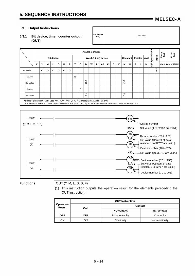
5. SEQUENCE INSTRUCTIONS
5 − 14
MELSEC-A
5.3 Output Instructions
5.3.1 Bit device, timer, counter output(OUT)
Available Device
Bit device Word (16-bit) device Constant Pointer Level Car
ryfla
g
Erro
rfla
g
X Y M L S B F T C D W R A0 A1 Z V K H P I N
Digi
t spe
cific
atio
n
Inde
x
M9012 (M9010, M9011)
Bit device O O O O O O
Device O
Set Value O O
Device O
Set value O O
*1: Index qualification can be used AnA, A2AS, AnU, QCPU-A (A Mode) and A2USH board only.*2: If extension timers or counters are used with the AnA, A2AS, AnU, QCPU-A (A Mode) and A2USH board, refer to Section 3.8.3.
Functions OUT (Y, M, L, S, B, F)(1) This instruction outputs the operation result for the elements pereceding the
OUT instruction.
OUT Instruction
ContactOperationResult Coil
NO contact NC contact
OFF OFF Non-continuity Continuity
ON ON Continuity Non-continuity
ApplicableCPU All CPUs
*2
*2
*2
*2
*1
OUT
OUT
OUT
(Y, M, L, S, B, F)
(T)
(C)
Y35
Device number
T0
Set value (Content of dataresister. 1 to 32767 are valid.)
K50 Set value (1 to 32767 are valid.)
Set value (1to 32767 are valid.)
Device number (T0 to 255)D10
Device number (T0 to 255)T0
K50
Set value (Content of dataresister. 1 to 32767 are valid.)
C0Device number (C0 to 255)
D10C1
Device number (C0 to 255)

5. SEQUENCE INSTRUCTIONS
5 − 15
MELSEC-A
POINTS
(1) When F (annunciator) is turned ON, LED indicators and ERROR LEDs onthe CPU module illuminate, and the number of annunciator which isturned ON is stored in special registers. For details, refer to the ACPUProgramming Manual (Fundamentals).
(2) If the OUT instruction is used to turn ON the annunciator, annunciator coilstatus does not correspond to the display of LED indicators. To avoid this,use the SET instruction to turn ON the annunciator.If the OUT instruction is used to turn ON the annunciator, the annunciatorcoil turns OFF when the operation result of instructions preceding the OUTinstruction turns OFF. However, display contents of LED indicators andERROR LEDs on the CPU module and contents of special registers donot change.For details, refer to the ACPU Programming Manual (Fundamentals).
REMARK
The number of steps is 3 when either of the following devices is used for OUT instruction:• Special relay (M)• Annunciator (F)
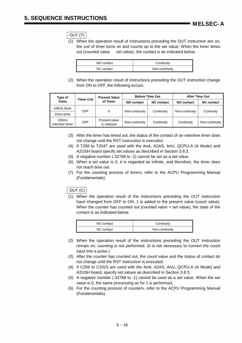
5. SEQUENCE INSTRUCTIONS
5 − 16
MELSEC-A
OUT (T)(1) When the operation result of instructions preceding the OUT instruction are on,
the coil of timer turns on and counts up to the set value. When the timer timesout (counted value � set value), the contact is as indicated below.
NO contact Continuity
NC contact Non-continuity
(2) When the operation result of instructions preceding the OUT instruction changefrom ON to OFF, the following occurs.
Before TIme Out After Time OutType ofTimer Timer Coil Present Value
of Timer NO contact NC contact NO contact NC contact
100ms timer
10ms timerOFF 0 Non-continuity Continuity Non-continuity Coninuity
100msretentive timer OFF Present value
is retained Non-continuity Continuity Continuity Non-continuity
(3) After the timer has timed out, the status of the contact of an retentive timer doesnot change until the RST instruction is executed.
(4) If T256 to T2047 are used with the AnA, A2AS, AnU, QCPU-A (A Mode) andA2USH board specify set values as described in Section 3.8.3.
(5) A negative number (-32768 to -1) cannot be set as a set value.(6) When a set value is 0, it is regarded as infinite, and therefore, the timer does
not reach time out.(7) For the counting process of timers, refer to the ACPU Programming Manual
(Fundamentals).
OUT (C)(1) When the operation result of the instructions preceding the OUT instruction
have changed from OFF to ON, 1 is added to the present value (count value).When the counter has counted out (counted value = set value), the state of thecontact is as indicated below.
NO contact Continuity
NC contact Non-continuity
(2) When the operation result of the instructions preceding the OUT instructionremain on, counting is not performed. (It is not necessary to convert the countinput into a pulse.)
(3) After the counter has counted out, the count value and the status of contact donot change until the RST instruction is executed.
(4) If C256 to C1023 are used with the AnA, A2AS, AnU, QCPU-A (A Mode) andA2USH board, specify set values as described in Section 3.8.3.
(5) A negative number (-32768 to -1) cannot be used as a set value. When the setvalue is 0, the same processing as for 1 is performed.
(6) For the counting process of counters, refer to the ACPU Programming Manual(Fundamentals).
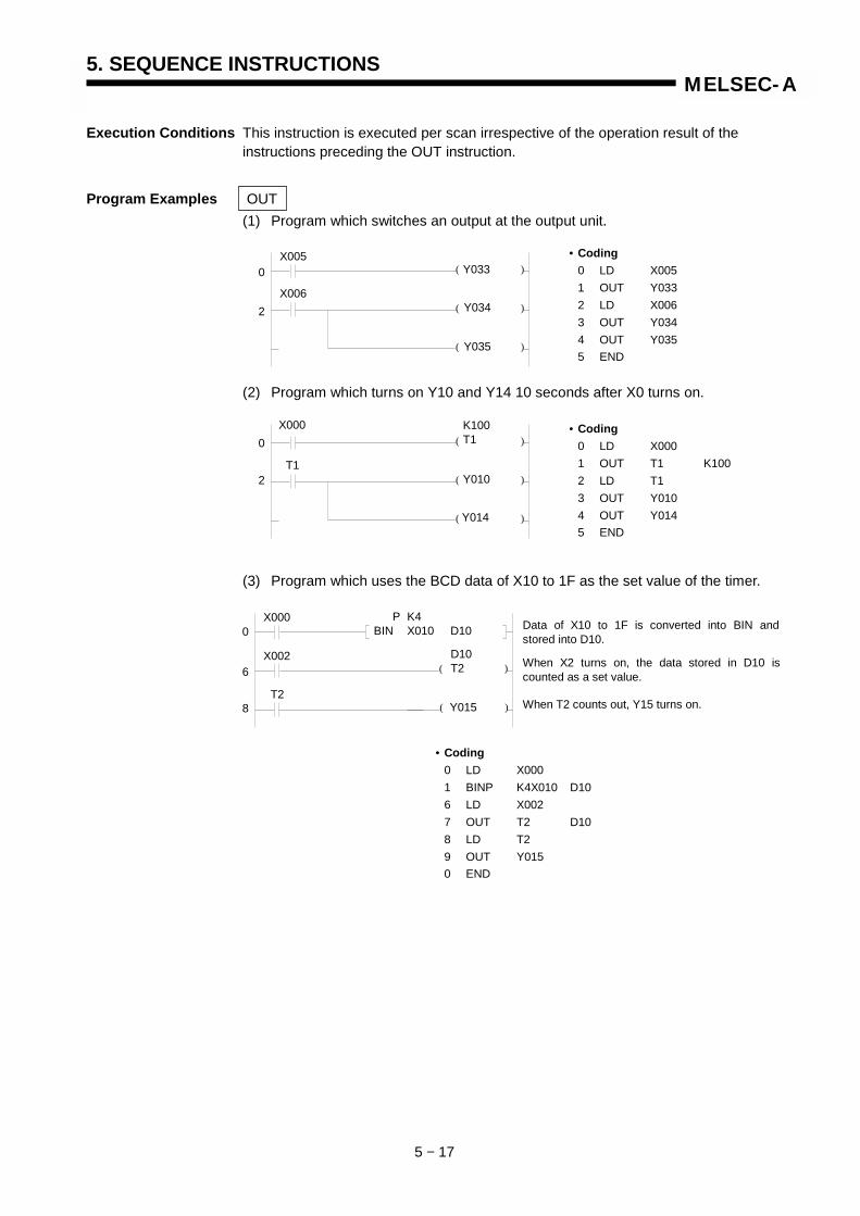
5. SEQUENCE INSTRUCTIONS
5 − 17
MELSEC-A
Execution Conditions This instruction is executed per scan irrespective of the operation result of the instructions preceding the OUT instruction.
Program Examples OUT(1) Program which switches an output at the output unit.
(2) Program which turns on Y10 and Y14 10 seconds after X0 turns on.
(3) Program which uses the BCD data of X10 to 1F as the set value of the timer.
• Coding0 LD X0051 OUT Y0332 LD X0063 OUT Y0344 OUT Y0355 END
• Coding0 LD X0001 OUT T1 K1002 LD T13 OUT Y0104 OUT Y0145 END
( )
( )
( )
X005
X006
Y033
Y034
Y035
0
2
X000( )
( )
( )
T1
K100T1
Y010
Y014
0
2
Data of X10 to 1F is converted into BIN andstored into D10.
( )
( )
0
6
8 Y015
X000
X002
T2
P K4BIN X010 D10
D10T2
• Coding0 LD X0001 BINP K4X010 D106 LD X0027 OUT T2 D108 LD T29 OUT Y0150 END
When T2 counts out, Y15 turns on.
When X2 turns on, the data stored in D10 iscounted as a set value.

5. SEQUENCE INSTRUCTIONS
5 − 18
MELSEC-A
(4) Program which turns on Y30 after X0 turns on 10 times and which turns off Y30 when X1 turns on.
(5) Program which changes the set value of C10 to 10 when X0 turns on and to 20 when X1 turns on.
( )
( )
0
2
4X001
X000
C10
K10C10
Y030
RST C10
• Coding0 LD X0001 OUT C10 K102 LD C103 OUT Y0304 LD X0015 RST C108 END
When X1 turns on, 20 is stored to D0.
When X0 turns on, 10 is stored to D0.
( )
( )
0
6
12
14C10
X000
X001
X003
P KMOV 10 D0
Y030
D0C10
P KMOV 20 D0
C10 counts the data, which is stored in D0, asa set value.
When C10 counts out, Y30 turns on.
• Coding0 LD X0001 MOVP K10 D06 LD X0017 MOVP K20 D0
12 LD X00313 OUT C10 D014 LD C1015 OUT Y03016 END

MEMO
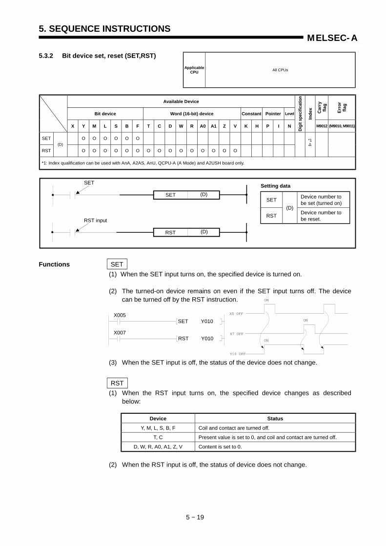
5. SEQUENCE INSTRUCTIONS
5 − 19
MELSEC-A
5.3.2 Bit device set, reset (SET,RST)
Available Device
Bit device Word (16-bit) device Constant Pointer Level Car
ryfla
g
Erro
rfla
g
X Y M L S B F T C D W R A0 A1 Z V K H P I N
Digi
t spe
cific
atio
n
Inde
x
M9012 (M9010, M9011)
SET O O O O O O
RST(D)
O O O O O O O O O O O O O O O
*1: Index qualification can be used with AnA, A2AS, AnU, QCPU-A (A Mode) and A2USH board only.
Functions SET(1) When the SET input turns on, the specified device is turned on.
(2) The turned-on device remains on even if the SET input turns off. The devicecan be turned off by the RST instruction.
(3) When the SET input is off, the status of the device does not change.
RST(1) When the RST input turns on, the specified device changes as described
below:
Device Status
Y, M, L, S, B, F Coil and contact are turned off.
T, C Present value is set to 0, and coil and contact are turned off.
D, W, R, A0, A1, Z, V Content is set to 0.
(2) When the RST input is off, the status of device does not change.
ApplicableCPU All CPUs
*1
X5 OFF
X7 OFF
Y10 OFF
ON
ON
ON
X005
X007
SET Y010
RST Y010
SET Device number tobe set (turned on)
RST(D)
Device number tobe reset.
Setting dataSET
RST input
SET
RST
(D)
(D)

5. SEQUENCE INSTRUCTIONS
5 − 20
MELSEC-A
(3) The functions of RST (D, W, R, A0, A1, Z, V) are the same as those of thefollowing circuit.
If the annunciator relay (F ) is turned ON/OFF, display contents of LED indicatorsand ERROR LEDs on the CPU module and contents of special registers change.For details, refer to the ACPU Programming Manual (Fundamentals).
Execution (1) The SET, RST instructions are executed on the following conditions:Conditions
(2) SET, RST instructionsIn refresh mode, the SET/RST instructions cannot be used in a program whichoutputs a pulse signal during one scan. In this case, output (Y) must bechanged to direct mode or add the partial refresh command as shown below.
REMARK
The number of steps is 3 when any of the following devices is used:
SET instruction Special relay (M)Link relay (B)Annunciator (F)
RST instruction Special relay (M)Word devices (All)
RST inputRST input
Device number(D, W, R, A0, A1, Z, V)
Device number(D, W, R, A0, A1, Z, V)
X010RST D50
X010 KMOV 0 D50
Direct mode Refresh mode
SET, RSTinstruction
SET, RST (Y, M, L, S, B)
SET, RST (F)
OFF
ON
Executed every scanExecutedever scan
Executedonly once
Executed onlyonce
ON
OFF
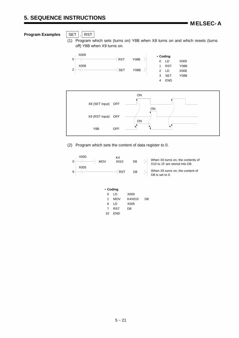
5. SEQUENCE INSTRUCTIONS
5 − 21
MELSEC-A
Program Examples SET , RST(1) Program which sets (turns on) Y8B when X8 turns on and which resets (turns
off) Y8B when X9 turns on.
(2) Program which sets the content of data register to 0.
• Coding0 LD X0001 MOV K4X010 D86 LD X0057 RST D8
10 END
When X0 turns on, the contents ofX10 to 1F are stored into D8.
When X5 turns on, the content ofD8 is set to 0.
K4MOV X010 D8
RST D8
0
6
• Coding0 LD X0091 RST Y08B2 LD X0083 SET Y08B4 END
X009
X008
RST Y08B
SET Y08B
0
2
X8 (SET input) OFF
X9 (RST input) OFF
Y8B OFF
ON
ON
ON
X000
X005

5. SEQUENCE INSTRUCTIONS
5 − 22
MELSEC-A
(3) Program which resets the 100ms retentive timer and counter.
• Coding0 LD X0041 OUT T225 K180002 LD T2253 OUT C23 K164 RST T2257 LD C238 OUT Y0559 LD X005
10 RST C2313 END
( )
( )
( ) T225 turns on after X4 has beenon for 30 minutes.
The number of ON times of T225is counted.
When T225 has turned on, T225 is reset.
When C23 has counted up, Y55 turnes on.
When X5 turns on, C23 is reset.
X004
T225
C23
X005
K18000T225
K16C23
RST T225
RST C23
Y055
0
2
7
9

5. SEQUENCE INSTRUCTIONS
5 − 23
MELSEC-A
5.3.3 Edge-triggered differential output(PLS, PLF)
Available Device
Bit device Word (16-bit) device Constant Pointer Level Car
ryfla
g
Erro
rfla
g
X Y M L S B F T C D W R A0 A1 Z V K H P I N
Digi
t spe
cific
atio
n
Inde
x
M9012 (M9010, M9011)
(D) O O O O O O
*1: Index qualification can be used with AnA, A2AS, AnU, QCPU-A (A Mode) and A2USH board only.
Function PLS(1) When the PLS command changes from Off to On, the specified device goes On
for 1 scan and when the PLS command is in a state other than Off → On (Off →Off, On → On, On → Off), the device goes Off.If there is one PLS instruction from the specified device (D) within 1 scan, thespecified device goes On for 1 scan.See Section 3.9 concerning operation in the case that the PLS instruction fromthe same device is executed multiple times in 1 scan.
(2) If the instruction generating the pulse is switched on and the RUN key switch ismoved from the RUN to STOP position and the RUN key switch is moved fromthe RUN to STOP position and then returned to the RUN position again, thePLS instruction is not executed.
PLS command
X005PLS M0
X000PLS M0
Move RUN key switchof CPU unit fromRUN to STOP position
Move RUN key switchof CPU unit fromSTOP to RUN position
PLS
PLS
PLS command
M0 OFF
X5 OFF
ON
ON
1 scan
ApplicableCPU All CPUs
(3) When a latch relay (L) is specified in a PLS instruction execution command,after the power goes Off with the latch relay (L) in the On state, when the poweris turned On again, the PLS command executes the PLS command so that it willchange from Off to On in the first scan and turn the specified device On. Afterthe power goes On, the device which was turned On in the first scan goes Offwhen the next PLS instruction is executed.
PLF command
(D)
(D)
(D) Device number to be con-verted into pulse
Setting data
X0 OFF
M0 OFF
ON
PLS M0LD X0
END0END PLS M0LD X0
END PLS M0LD X0
0
ON
1scan of PLS M0
Operation stop timeof PC
Operation stop time of PC
1 scan
*1

5. SEQUENCE INSTRUCTIONS
5 − 24
MELSEC-A
PLF(1) When the PLF command changes from On to Off, the specified device goes On
for 1 scan and when the PLF command is in a state other than On → Off (Off →Off, Off → On, On → On), the device goes Off.If there is one PLF instruction from the specified device (D) within 1 scan, thespecified device goes On for 1 scan.See Section 3.9 concerning operation in the case that the PLF instruction fromthe same device is executed multiple times in 1 scan.
(2) If the instruction generating the pulse is off and the RUN key switch is movedfrom the RUN to STOP position and then returned to the RUN position again,the PLF instruction is not executed.
POINT
If a PLS or PLF instruction is caused to jump by a CJ instruction, if the sub-routine program executed by a PLS/PLF command was not called by a CALLinstruction, the device specified by (D) will go On for 1 scan or longer, soexercise caution.
Program Examples PLSProgram which executes the PLS instruction when M9 turns on.
PLFProgram which executes the PLF instruction when M9 turns off.
X005PLF M0
• Coding0 LD X0091 PLS M94 ENDON
X9 OFF
M9 OFF
ON
1 scan
• Coding0 LD X0091 PLF M94 END
X5 OFF
M0 OFF
ON
ON
1 scan 1 scan
X009PLS M90
X009PLF M90
M9 OFF
ON
1 scan
ON
X9 OFF

5. SEQUENCE INSTRUCTIONS
5 − 25
MELSEC-A
5.3.4 Bit device output reverse (CHK)
The CHK instruction varies in function with I/0 control mode as shown below.
I/O control modeCPU
Direct mode Refresh mode(when either or both of input and output are in refresh mode)
An Failure check
AnN, AnS, AnSH, A1FX,A0J2H, A73, A3N board Failure check Bit device output reverse
A3H, A3M Failure check Failure check
A3V, AnA,A2C, A52G, AnU, A2AS, QCPU-
A (A Mode), A2USH board Failure check
For failure check, refer to Section 7.10.2.
Available Device
Bit device Word (16-bit) device Constant Pointer Level Car
ryfla
g
Erro
rfla
g
X Y M L S B F T C D W R A0 A1 Z V K H P I N
Digi
t spe
cific
atio
n
Inde
x
M9012 (M9010, M9011)
(D1) O O O O O O
(D2)
*1: Device used for D2 is a dummy data which has nothing to do with program processing.
AnSAnN
AnSHAn A1FX A3H
A3M A3V AnA
AnU, A2ASA2USH-S1
A2USH boardQCPU-A(A Mode)
A0J2H A2CA52G A73 A3N
boadApplicableCPU
x O x x x x x
Remark * Valid only when the input/output control method is refresh method.
*1 *1 *1 *1 *1 *1 *1 *1 *1 *1 *1 *1 *1 *1 *1
Output reverse command
CHK (D1) (D2)
(D1) Required device number
(D2)Dummy dataAny device number indi-cated by
K1toK4
Setting data
* * * *

5. SEQUENCE INSTRUCTIONS
5 − 26
MELSEC-A
Functions (1) Reverses the output status of the device, (D1), on the leading edge of theoutput reverse command.
(2) Though (D2) is a dummy data, specify any device number indicated with the mark for it. If a bit device is specified for (D2) , specify the digit with K1 to K4.Specify any value since this digit specification value is a dummy data.
Device specified for (D2) can be used freely for other purposes.
(3) The CHK instruction is only executed in refresh mode.
(4) The output reverse command on/off period must be equal or greater than 1scan time.
Program Example CHKThe following program reverses the output status of Y10 when X9 is switched on.
X005 K4CHK Y010 M1
X5 OFF
Y10 ON
OFF
ON
0X009
CHK Y010 D0• Coding
0 LD X0091 CHK Y010 D06 END

5. SEQUENCE INSTRUCTIONS
5 − 27
MELSEC-A
5.4 Shift Instructions
5.4.1 Bit device shift (SFT, SFTP)
Available Device
Bit device Word (16-bit) device Constant Pointer Level Car
ryfla
g
Erro
rfla
g
X Y M L S B F T C D W R A0 A1 Z V K H P I N
Digi
t spe
cific
atio
n
Inde
x
M9012 (M9010, M9011)
(D) O O O O O O
*1: Index qualification can be used with AnA, A2AS, AnU, QCPU-A (A Mode) and A2USH board only.
Functions (1) This instruction shifts the ON/OFF status of a device number, (defined as D-1) to the device specified as D and turns off the device with the lower number.
(2) Turn on the head device to be shifted with the SET instruction.
(3) When the SFT or SFTP instruction is used consecutively, program higherdevice numbers first. (See below.)
Setting data
*1
ApplicableCPU All CPUs
SFT
SFTP
(D)
(D)
SFT instruction
������������������
����������������
����������������
������������������
����������������
����������������
����������������
����������������
����������������
������������������������
M15 M14 M13 M12 M11 M10 M9
00 0 0 0 1 1 0
M8
00 1 0 0 0 1 0
00 0 0 1 0 1 0
00 0 1 0 0 1 0
00 0 1 0 1 1 0
00 1 0 1 0 1 0
10 0 1 0 0 1 0
1)
2)
3)
4)
5)
6)
7)
After the second shift input
X2 ON
After the first shift input
X2 ON
After the third shift input
After the fourth shift input
After the fifth shift input
Shift range
*: At M8 to 15, 1 indicates ON and 0 indicates OFF.
Shift input
M0
X002
PSFT M14
PSFT M13
PSFT M12
PSFT M11
SFT M10
(D) Device number to beshifted

5. SEQUENCE INSTRUCTIONS
5 − 28
MELSEC-A
Program Example SFT(1) Program which shifts the Y57 to 5B when X8 turns on.
OFFX8
X7
Y57
Y58
Y59
Y5A
Y5B
ON
OFF
OFF
OFF
OFF
OFF
OFF
ON
ON
ON
ON
ON
ON
• Coding0 LD X0081 SFTP Y05B4 STFP Y05A7 SFTP Y059
10 SFTP Y05813 LD X00714 PLS M817 LD M818 SET Y05719 END
X0080
PSFT Y05B
PSFT Y05A
PSFT Y059
PSFT Y058
PLS M8
SET Y057
When X8 turns on, shift is executed.(Perform programming in order oflarger device numbers.)
When X7 turns on, Y57 isturned on.
13
17
X007
M8

5. SEQUENCE INSTRUCTIONS
5 − 29
MELSEC-A
5.5 Master Control Instructions
5.5.1 Master control set, reset (MC, MCR)
Available Device
Bit device Word (16-bit) device Constant Pointer Level Car
ryfla
g
Erro
rfla
g
X Y M L S B F T C D W R A0 A1 Z V K H P I N
Digi
t spe
cific
atio
n
Inde
x
M9012 (M9010, M9011)
n O
(D) O O O O O O
*1: Index qualification can be used with AnA, A2AS, AnU, QCPU-A (A Mode) and A2USH board only.
Functions The MC instruction is used to allow the sequence program to perform efficient circuitswitching by opening and closing the common bus of circuits. The figure below shows an example of circuit when the MC instruction is used.
REMARK
When a program is written in the ladder mode of GPP, it is not necessary to input contacts onthe bus. Those contacts are displayed automatically by performing conversion.
*1
ApplicableCPU All CPUs
ON/OFF command for MC
MC
MCR
n
n
(D)
n Nesting (N0 to 7)
(D) Device number to beturned on
Setting data(D) ← Device
Nesting (N0 to 7)
n
MC N1 M0
Y47
Y4F
Y40
X0
X1
M5
X6
X3 M7
X4
XF
MCR N1
N1 M0
( )
( )
( )
Circuit in the ladder mode of GPP Actual operation circuit
Executedonly whenX0 is ON.
X000
N1 M0
MC N1 M0
Y047
Y04F
X001 X003 M7
M5
X006 X004
MCR N1
Y010X00F
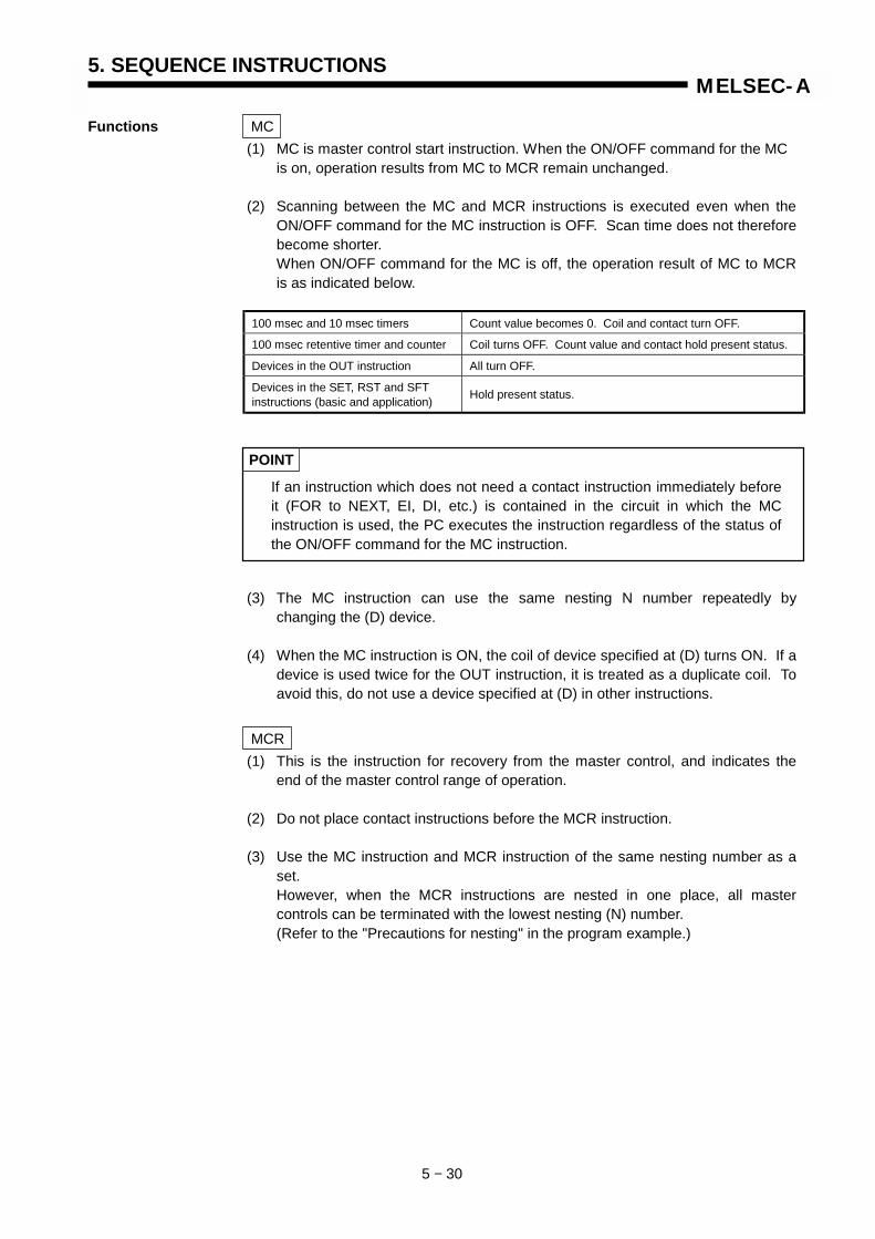
5. SEQUENCE INSTRUCTIONS
5 − 30
MELSEC-A
Functions MC(1) MC is master control start instruction. When the ON/OFF command for the MC
is on, operation results from MC to MCR remain unchanged.
(2) Scanning between the MC and MCR instructions is executed even when theON/OFF command for the MC instruction is OFF. Scan time does not thereforebecome shorter.When ON/OFF command for the MC is off, the operation result of MC to MCRis as indicated below.
100 msec and 10 msec timers Count value becomes 0. Coil and contact turn OFF.
100 msec retentive timer and counter Coil turns OFF. Count value and contact hold present status.
Devices in the OUT instruction All turn OFF.
Devices in the SET, RST and SFTinstructions (basic and application) Hold present status.
POINT
If an instruction which does not need a contact instruction immediately beforeit (FOR to NEXT, EI, DI, etc.) is contained in the circuit in which the MCinstruction is used, the PC executes the instruction regardless of the status ofthe ON/OFF command for the MC instruction.
(3) The MC instruction can use the same nesting N number repeatedly bychanging the (D) device.
(4) When the MC instruction is ON, the coil of device specified at (D) turns ON. If adevice is used twice for the OUT instruction, it is treated as a duplicate coil. Toavoid this, do not use a device specified at (D) in other instructions.
MCR(1) This is the instruction for recovery from the master control, and indicates the
end of the master control range of operation.
(2) Do not place contact instructions before the MCR instruction.
(3) Use the MC instruction and MCR instruction of the same nesting number as aset.However, when the MCR instructions are nested in one place, all mastercontrols can be terminated with the lowest nesting (N) number.(Refer to the "Precautions for nesting" in the program example.)
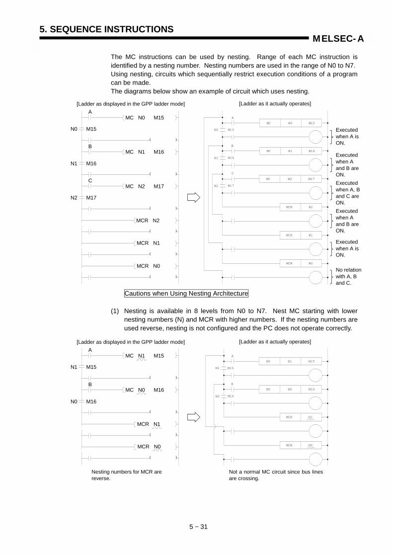
5. SEQUENCE INSTRUCTIONS
5 − 31
MELSEC-A
The MC instructions can be used by nesting. Range of each MC instruction isidentified by a nesting number. Nesting numbers are used in the range of N0 to N7.Using nesting, circuits which sequentially restrict execution conditions of a programcan be made.The diagrams below show an example of circuit which uses nesting.
Cautions when Using Nesting Architecture
(1) Nesting is available in 8 levels from N0 to N7. Nest MC starting with lowernesting numbers (N) and MCR with higher numbers. If the nesting numbers areused reverse, nesting is not configured and the PC does not operate correctly.
( )
( )
( )
( )
( )
( )
MC N0 M15
A
M15
B
C
M17
N0
MCR N2
MCR N1
MCR N0
MC N1 M16
MC N2 M17
N1
N2
M16
[Ladder as displayed in the GPP ladder mode] [Ladder as it actually operates]
Executedwhen A isON.
A
N0 M15
MC N0 M15
Executedwhen Aand B areON.Executedwhen A, Band C areON.Executedwhen Aand B areON.
Executedwhen A isON.
No relationwith A, Band C.
B
N1 M16
MC N1 M16
C
N2 M17
MC N2 M17
MCR N2
MCR N1
MCR N0
( )
( )
( )
( )
MC N1 M15
A
M15
B
N1
MCR N1
MCR N0
MC N0 M16
N0 M16
[Ladder as displayed in the GPP ladder mode] [Ladder as it actually operates]A
N1 M15
MC N1 M15
B
N0 M16
MC N0 M16
MCR N1
MCR N0
Nesting numbers for MCR arereverse.
Not a normal MC circuit since bus linesare crossing.

5. SEQUENCE INSTRUCTIONS
5 − 32
MELSEC-A
(2) If the MCR instructions gather at one place of nesting, use the lowest nestingnumber (N) once to end all MCs.
( )
( )
( )
( )
( )
( )
( )
( )
X001
N0 M15
MC N0 M15
X002
N1 M16
MC N1 M16
X003
N2 M17
MC N2 M17
MCR N2
MCR N1
MCR N0
X001
N0 M15
MC N0 M15
X002
N1 M16
MC N1 M16
X003
N2 M17
MC N2 M17
MCR N0

5. SEQUENCE INSTRUCTIONS
5 − 33
MELSEC-A
5.6 Termination Instructions
5.6.1 Main routine program termination(FEND)
Available Device
Bit device Word (16-bit) device Constant Pointer Level Car
ryfla
g
Erro
rfla
g
X Y M L S B F T C D W R A0 A1 Z V K H P I N
Digi
t spe
cific
atio
n
Inde
x
M9012 (M9010, M9011)
O
Functions (1) Terminates the main routine program.
(2) When the FEND instruction is executed, the PC returns to step 0 after theprocessing (such as timer/counter processing and self-diagnostic check) afterthe execution of END instruction, and resumes operation from step 0.
(3) The sequence program located after FEND instruction can also be displayed onthe GPP. (The GPP displays a circuit up to the END instruction.)
Operation Errors In the following cases, operation error occurs and the PC stops its operation.• After the CALL(P) instruction is executed, the FEND instruction has been
executed before executing the RET instruction.• After the FOR instruction is executed, the FEND instruction has been executed
before executing the NEXT instruction.
ApplicableCPU All CPUs
FEND
CJ
FEND
FEND
END
0 CALL
FEND
END
P**
P**
P**
P**
I**
Operation whenCJ instruction isnot exectuted
Main routineprogram
Main routineprogram
Main routineprogram
Jump by CJinstruction
Operation whenCJ instruction isexecuted
(a) By use of CJ instruction
Main routineprogram
Subroutineprogram
Interrupt program
(b) There are subroutine programand interrupt program
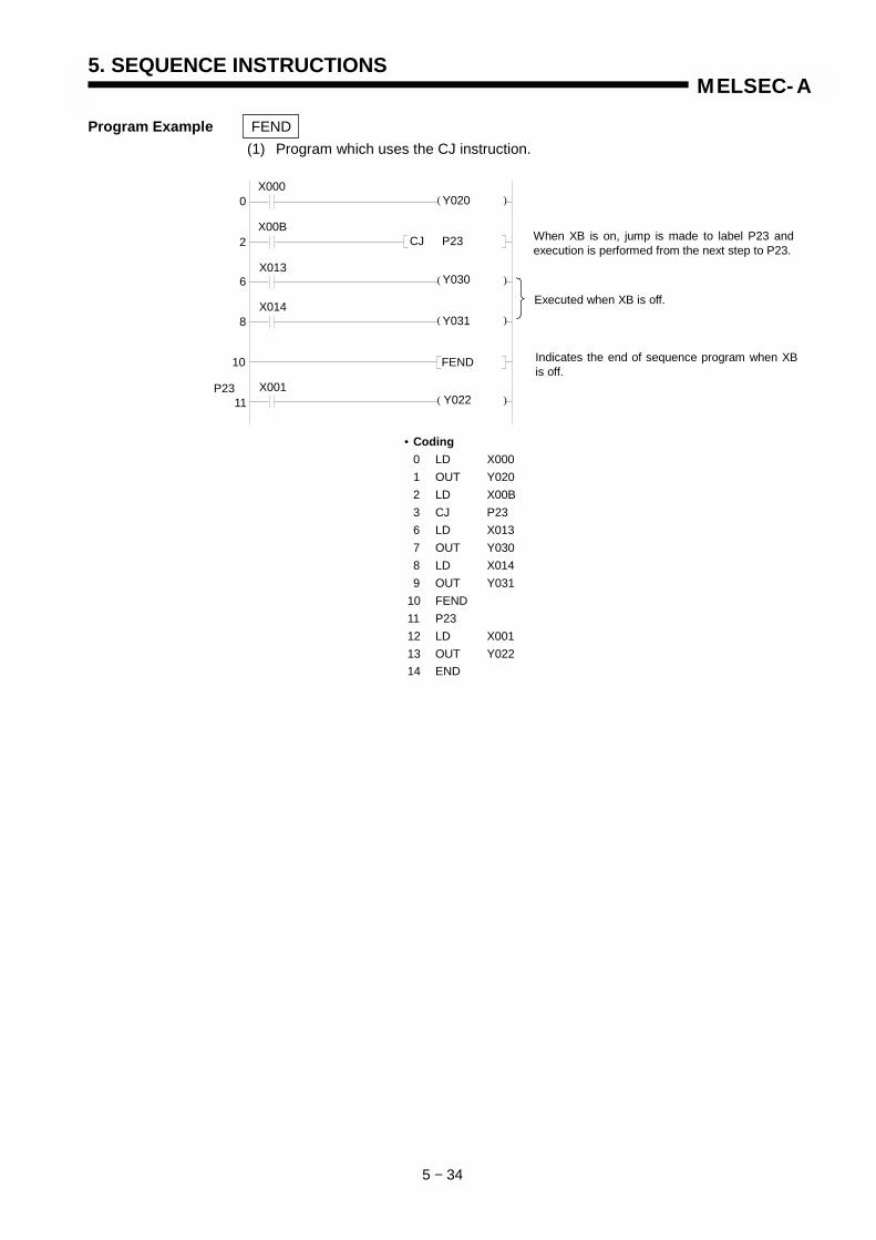
5. SEQUENCE INSTRUCTIONS
5 − 34
MELSEC-A
Program Example FEND(1) Program which uses the CJ instruction.
( )
( )
( )
( )
X0000 Y020
X00B2 CJ P23
X0136
When XB is on, jump is made to label P23 andexecution is performed from the next step to P23.
Y030
X0148 Y031
Executed when XB is off.
10 FEND
X001P2311
Indicates the end of sequence program when XBis off.
Y022
• Coding0 LD X0001 OUT Y0202 LD X00B3 CJ P236 LD X0137 OUT Y0308 LD X0149 OUT Y031
10 FEND11 P2312 LD X00113 OUT Y02214 END

5. SEQUENCE INSTRUCTIONS
5 − 35
MELSEC-A
5.6.2 Sequence program termination (END)
Available Device
Bit device Word (16-bit) device Constant Pointer Level Car
ryfla
g
Erro
rfla
g
X Y M L S B F T C D W R A0 A1 Z V K H P I N
Digi
t spe
cific
atio
n
Inde
x
M9012 (M9010, M9011)
Functions (1) This instruction indicates the end of program. At this step, the scan returns to step 0.
(2) The END instruction cannot be used midway through the sequence program orsubsequence program. If END processing is necessary halfway through theprogram, use the FEND instruction.
(3) When a program is written in the ladder mode of GPP, it is not necessary toinput the END instruction. It is input automatically by performing conversion.
0
ApplicableCPU All CPUs
END
When the ladder is displayed,END is omitted.
Sequence program
END

5. SEQUENCE INSTRUCTIONS
5 − 36
MELSEC-A
(4) Use the END and FEND instructions in the main routine program, subroutineprogram, interrupt program, and subsequence program as shown below.
Fig. 5.1 Use of the END (FEND) Instructions
(5) If the END instruction is not given in the program, operation error occurs andthe PC does not run. If parameters are used to set subprogram capacity,operation error occurs when the END instruction is not given in the subprogram.
Operation Errors In the following cases, operation error occurs and the PC stops its operation.
(1) Jump has been made to a step below the END instruction by the CJ, SCJ, orJMP instruction.
(2) The subroutine program or interrupt program located below the END instructionhas been executed.
Main routine program
Subroutine program
(FEND instruction is always required.)
Main sequence programarea
Interrupt program
(END instruction is always required.)
Main routine program
(FEND instruction is always required.)
Subroutine program Subsequence programarea
Interrupt program
(END instruction is always required.
FEND
END
FEND
END

5. SEQUENCE INSTRUCTIONS
5 − 37
MELSEC-A
5.7 Other Instructions
5.7.1 Sequence program stop (STOP)
Available Device
Bit device Word (16-bit) device Constant Pointer Level Car
ryfla
g
Erro
rfla
g
X Y M L S B F T C D W R A0 A1 Z V K H P I N
Digi
t spe
cific
atio
n
Inde
x
M9012 (M9010, M9011)
Functions (1) When the stop input turns on, resets the outputs Y and stops the operation of PC. (The same function as when the RUN key switch is moved to the STOP position)
(2) When the STOP instruction is executed, B8 of the special register D9015 is setto 1.
(3) To resume the operation of PC after the execution of STOP instruction, movethe RUN key switch from the RUN to the STOP position and then move it to theRUN position again.
(4) Even if the RESET switch is moved to the “LATCH CLEAR” position when theSTOP instruction has been executed, latch clear is not executed. To executethe latch clear, move the RUN key switch to the STOP position and then movethe RESET switch to the “LATCH CLEAR” position.
(5) Do not provide the STOP instruction in the interrupt program, subroutineprogram, and FOR/NEXT. If the STOP instruction is provided, operation erroroccurs.
ApplicableCPU All CPUs
STOP
Stop input
Set to 1.
D9015
b0
0 0 0 0 0 0 0 1
b15 b14 b13 b12 b11b10 b9 b8
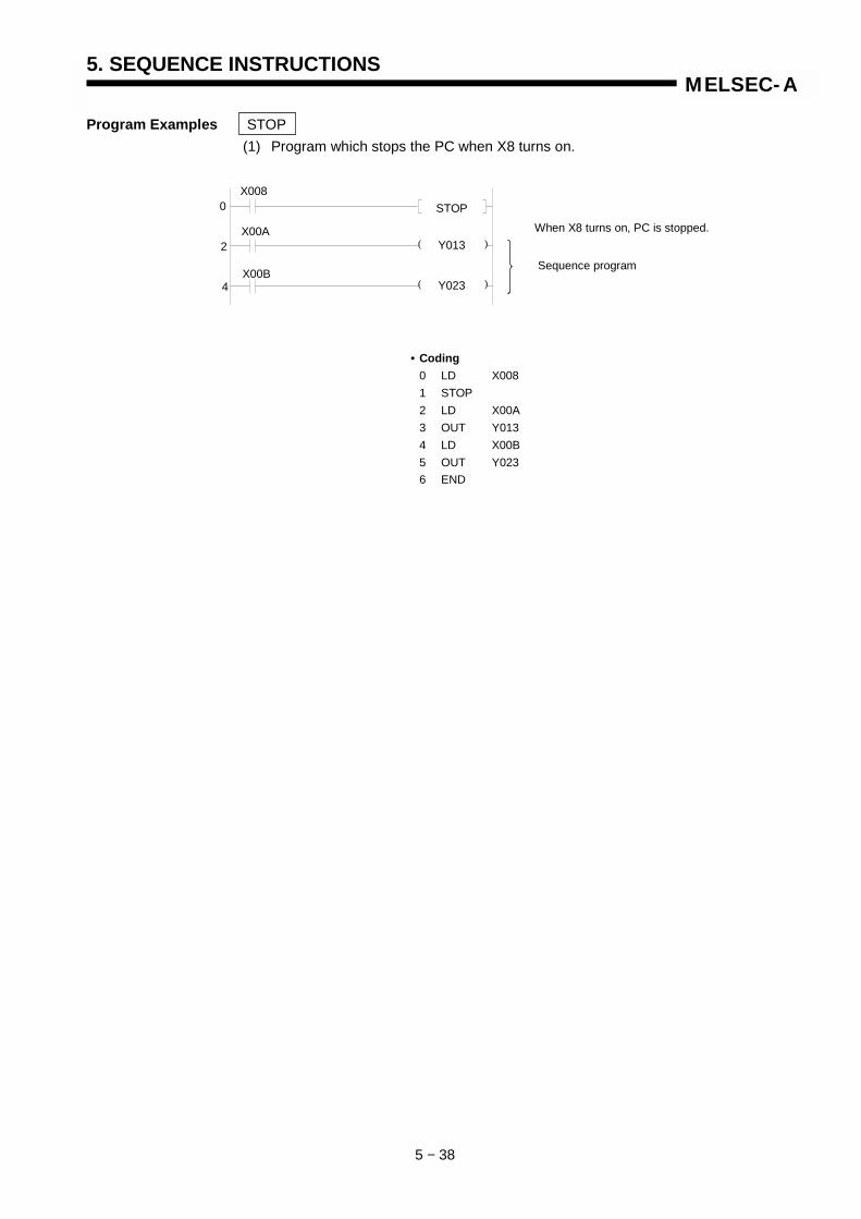
5. SEQUENCE INSTRUCTIONS
5 − 38
MELSEC-A
Program Examples STOP(1) Program which stops the PC when X8 turns on.
( )
( )
X008
X00A
X00B
STOP
Y013
Y023
0
2
4
When X8 turns on, PC is stopped.
Sequence program
• Coding0 LD X0081 STOP2 LD X00A3 OUT Y0134 LD X00B5 OUT Y0236 END

5. SEQUENCE INSTRUCTIONS
5 − 39
MELSEC-A
5.7.2 No operation (NOP, NOPLF)
The NOPLF instruction can be used with the GPP of which software is SW4GP-GPPA or SW01X-GPPAE.
Available Device
Bit device Word (16-bit) device Constant Pointer Level Car
ryfla
g
Erro
rfla
g
X Y M L S B F T C D W R A0 A1 Z V K H P I N
Digi
t spe
cific
atio
n
Inde
x
M9012 (M9010, M9011)
NOP
When the ladder is displayed, NOP is omitted.
NOPLF When the ladder is displayed, NOPLF is omitted.
Functions NOP
(1) This is a no-operation instruction and has no effect on the previous operation.(2) NOP is used in the following cases:
1) To provide space for debugging of sequence programs.2) To delete an instruction without changing the number of steps. (Overwrite
with NOP)3) To delete an instruction temporarily.
NOPLF
(1) This is a no-operation instruction and has no effect on the previous operation.(2) The NOPLF instruction is used to specify page and at a desired point during the
GPP printer output operation.1) For printing ladder diagrams
• Page is changed if the NOPLF instruction is given at the end of eachladder block. The NOPLF instruction given in a ladder block is ignored.
• The NOPLF instruction given in a ladder block is handled as follows ifconversion is performed in the ladder mode of the GPP.Deleted when the number of steps increses.Converted to NOP when the number of steps decreases.
2) For printing instuction lists• Page is changed after NOPLF is printed.
3) For the GPP printer output, refer to the Operating Manual for peripheraldevices.
ApplicableCPU All CPUs
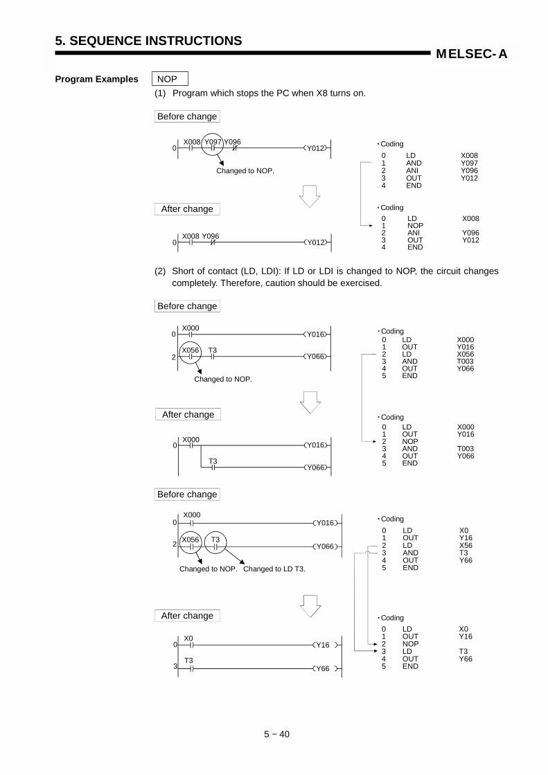
5. SEQUENCE INSTRUCTIONS
5 − 40
MELSEC-A
Program Examples NOP(1) Program which stops the PC when X8 turns on.
0X008
Y012Y097 Y096
Changed to NOP.
LDANDANIOUTEND
01234
X008Y097Y096Y012
0X008
Y012Y096
LDNOPANIOUTEND
01234
X008
Y096Y012
Before change
After change
Coding
Coding
(2) Short of contact (LD, LDI): If LD or LDI is changed to NOP, the circuit changescompletely. Therefore, caution should be exercised.
Before change
After change
0X000
Y016
2X056
Y066T3
LDOUTLDANDOUTEND
012345
X000Y016X056T003Y066
0X000
Y016
Y066T3
LDOUTNOPANDOUTEND
012345
X000Y016
T003Y066
Changed to NOP.
Coding
Coding
Before change
After change
0X000
Y016
2 X056Y066
T3
0X0
Y16
3T3
Y66
LDOUTLDANDOUTEND
012345
X0Y16X56T3Y66
LDOUTNOPLDOUTEND
012345
X0Y16
T3Y66
Coding
Coding
Changed to NOP. Changed to LD T3.
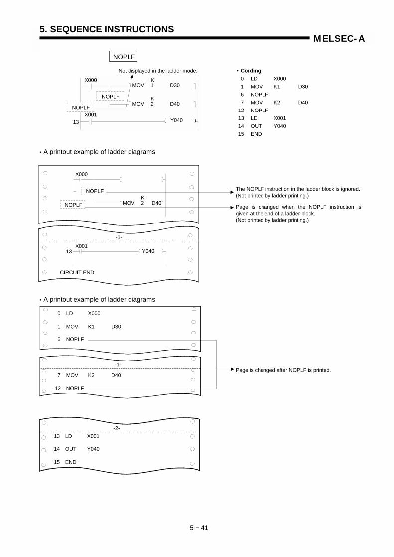
5. SEQUENCE INSTRUCTIONS
5 − 41
MELSEC-A
NOPLF
( )
• Cording0 LD X0001 MOV K1 D306 NOPLF7 MOV K2 D40
12 NOPLF13 LD X00114 OUT Y04015 END
• A printout example of ladder diagrams
The NOPLF instruction in the ladder block is ignored.(Not printed by ladder printing.)
Page is changed when the NOPLF instruction isgiven at the end of a ladder block.(Not printed by ladder printing.)
( )
X000
X00113
Not displayed in the ladder mode.
KMOV 1 D30
KMOV 2 D40
Y040
NOPLF
NOPLF
X000
NOPLFK
MOV 2 D40NOPLF
13 Y040
-1-X001
CIRCUIT END
• A printout example of ladder diagrams
-2-13 LD X001
14 OUT Y040
15 END
Page is changed after NOPLF is printed.
0 LD X000
1 MOV K1 D30
6 NOPLF
-1-
7 MOV K2 D40
12 NOPLF

6. BASIC INSTRUCTIONS
6 − 1
MELSEC-A
6. BASIC INSTRUCTIONS
The basic instructions are instructions which are capable of handing numeric dataexpressed in 16 bits and 32 bits, and are classified into the following instructions.
Classification of Basic Instructions Description Ref. Page
Comparison operation instruction Comparison such as =, >, and < 6-2
Arithmetic operation instructionAddition subtraction, multiplication,
and division in BIN and BCD.INC, DEC
6-8
BCD ↔ BIN conversion instruction Conversion from BCD to BIN andfrom BIN to BCD 6-38
Data transfer instruction Transfer of specified data 6-46
Program branch instruction Jump, call, interrupt enable/disable 6-58
Program switching instruction Switching between main and subprogram 6-69
Refresh instruction Data link refresh and I/O partial refresh 6-82

6. BASIC INSTRUCTIONS
6 − 2
MELSEC-A
6.1 Comparison Operation Instructions
(1) The comparison operation instructions make numerical magnitude comparisons(such as =, >, and <) between two pieces of data. They are handled as acontact, and turn on when their preceding condition holds.
(2) The application of comparison operation instruction is the same as that of thecontact instruction for the corresponding sequence instruction as indicatedbelow:• LD, LDI: LD =, LDD =• AND, ANI: AND =, ANDD =• OR, ORI: OR =, ORD =
(3) The comparison operation instructions are available in the following 36 types:
Classifica-tion
InstructionSymbol Ref. Page Classifica-
tionInstruction
Symbol Ref. Page Classifica-tion
InstructionSymbol Ref. Page
LD= LD> LD<
AND= AND> AND<
OR=
6-4
OR>
6-4
OR<
6-4
LDD= LDD> LDD<
ANDD= ANDD> ANDD<
=
ORD=
6-6
>
ORD>
6-6
<
ORD<
6-6
LD<> LD<= LD>=
AND<> AND<= AND>=
OR<>
6-4
OR<=
6-4
OR>=
6-4
LDD<> LDD<= LDD>=
ANDD<> ANDD<= ANDD>=
≠
ORD<>
6-6
≤
ORD<=
6-6
≥
ORD>=
6-6
(4) The conditions, by which the comparison operation instructions turn on, are asshown below.
Dn=K100 OFF ON OFFDn≠K100 ON OFF ONDn>K100 OFF ONDn≤K100 ON OFFDn<K100 ON OFFDn≥K100 OFF ON
98 99 100 101 102

6. BASIC INSTRUCTIONS
6 − 3
MELSEC-A
CAUTION
(1) The comparison instructions make the comparison, regarding the specified data as a BIN value. For this reason, in the case of comparison made in BCD value or hexadecimal, whena numeric value (8 to F) having 1 at the highest bit (B15 in a 16-bit instruction or B31 in a 32-bit instruction) is specifies, the comparison is made with the numeric value regarded as the negative of the BIN value.
Example
Comparison with 4-digit BCD value
Since the result is -30927<1384, Y10 does not turn ON.
(2) When the comparison of 32-bit data is made, specify the numeric value using the 32-bit instruction such as DMOV. If a 16-bit instruction such as MOV is used, comparison cannot be executed correctly.
Example
H8731 H0568 Y10>
Regarded as-30927 inBIN value.
Regarded as1384 in BINvalue.
( )
( )
107
D1 D0
79
D11 D10
>
256
D1 D0
?
D11 D10
?
M9036 KDMOV 107 D0
D> D0 D10 M5
KDMOV 79 D10
M9036 KDMOV 256 D0
D> D0 D10 M5
KMOV 86 D10
M5 turns ON.
Since values of 32-bit data D10 and D11are determined by content of D11, thecomparison result is unknown.
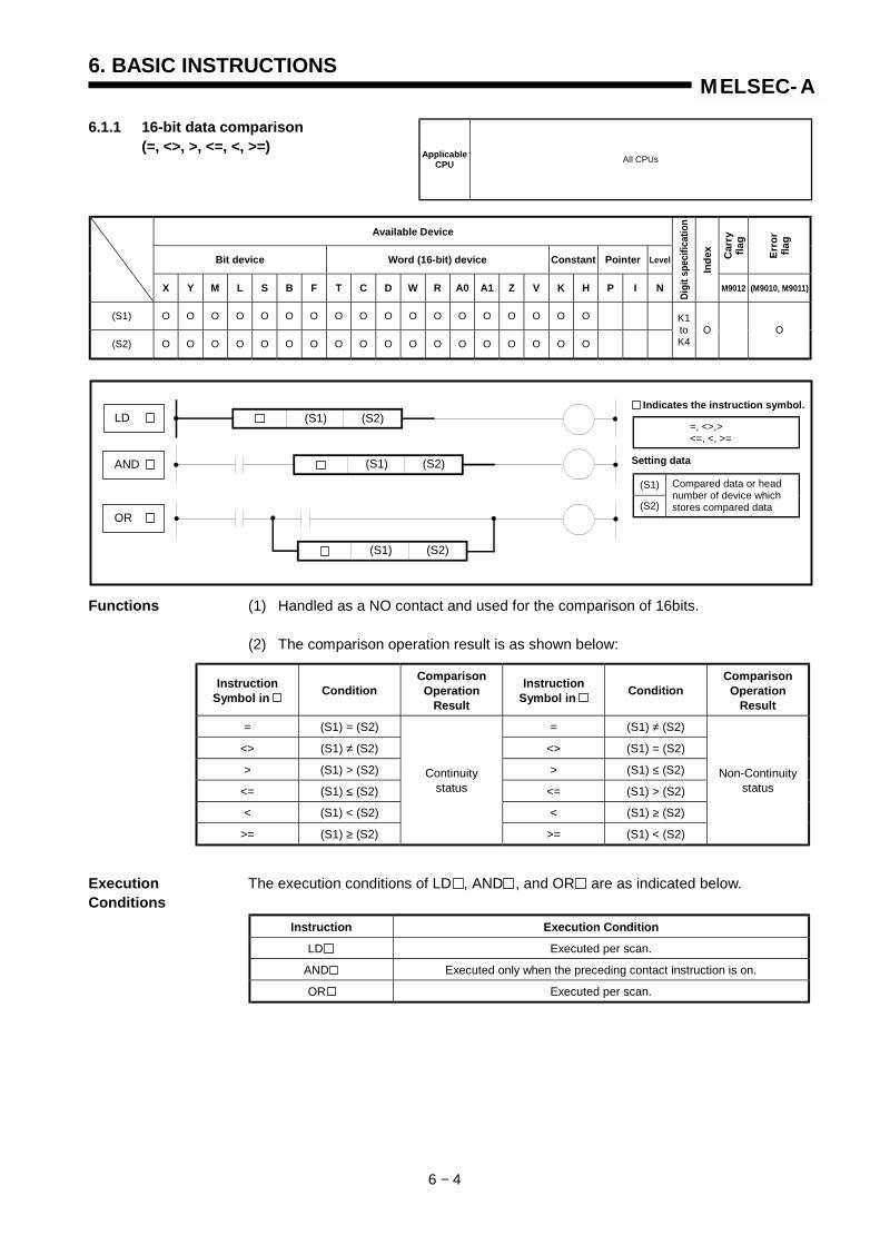
6. BASIC INSTRUCTIONS
6 − 4
MELSEC-A
6.1.1 16-bit data comparison(=, <>, >, <=, <, >=)
Available Device
Bit device Word (16-bit) device Constant Pointer Level Car
ryfla
g
Erro
rfla
g
X Y M L S B F T C D W R A0 A1 Z V K H P I N
Digi
t spe
cific
atio
n
Inde
x
M9012 (M9010, M9011)
(S1) O O O O O O O O O O O O O O O O O O
(S2) O O O O O O O O O O O O O O O O O O
K1toK4
O O
Functions (1) Handled as a NO contact and used for the comparison of 16bits.
(2) The comparison operation result is as shown below:
InstructionSymbol in Condition
ComparisonOperation
Result
InstructionSymbol in Condition
ComparisonOperation
Result
= (S1) = (S2) = (S1) ≠ (S2)
<> (S1) ≠ (S2) <> (S1) = (S2)
> (S1) > (S2) > (S1) ≤ (S2)
<= (S1) ≤ (S2) <= (S1) > (S2)
< (S1) < (S2) < (S1) ≥ (S2)
>= (S1) ≥ (S2)
Continuitystatus
>= (S1) < (S2)
Non-Continuitystatus
Execution The execution conditions of LD , AND , and OR are as indicated below.Conditions
Instruction Execution Condition
LD Executed per scan.
AND Executed only when the preceding contact instruction is on.
OR Executed per scan.
ApplicableCPU All CPUs
(S1)
(S2)
Compared data or headnumber of device whichstores compared data
Setting data
=, <>,><=, <, >=
Indicates the instruction symbol.LD
AND
OR
(S1) (S2)
(S1) (S2)
(S1) (S2)
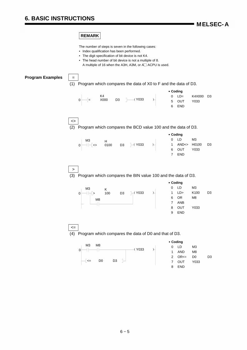
6. BASIC INSTRUCTIONS
6 − 5
MELSEC-A
REMARK
The number of steps is seven in the following cases:• Index qualification has been performed.• The digit specification of bit device is not K4.• The head number of bit device is not a multiple of 8.
A multiple of 16 when the A3H, A3M, or A ACPU is used.
Program Examples =(1) Program which compares the data of X0 to F and the data of D3.
<>(2) Program which compares the BCD value 100 and the data of D3.
>(3) Program which compares the BIN value 100 and the data of D3.
<=(4) Program which compares the data of D0 and that of D3.
( )0K4
= X000 D3 Y033
•••• Coding0 LD= K4X000 D35 OUT Y0336 END
( )0H
<> 0100 D3 Y033
•••• Coding0 LD M31 AND<> H0100 D36 OUT Y0337 END
M3
( )0K
> 100 D3 Y033
•••• Coding0 LD M31 LD> K100 D36 OR M87 ANB8 OUT Y0339 END
M3
M8
( )0
<= D0 D3
Y033
•••• Coding0 LD M31 AND M82 OR<= D0 D37 OUT Y0338 END
M3 M8

6. BASIC INSTRUCTIONS
6 − 6
MELSEC-A
6.1.2 32-bit data comparison(D=, D<>, D>, D<=, D<,D>=)
Available Device
Bit device Word (16-bit) device Constant Pointer Level Car
ryfla
g
Erro
rfla
g
X Y M L S B F T C D W R A0 A1 Z V K H P I N
Digi
t spe
cific
atio
n
Inde
x
M9012 (M9010, M9011)
(S1) O O O O O O O O O O O O O O O O
(S2) O O O O O O O O O O O O O O O O
K1toK8
O O
Functions (1) Handled as a NO contact and used for the comparison of 32bits.
(2) The comparison operation result is as shown below:
InstructionSymbol in Condition
ComparisonOperation
Result
InstructionSymbol in Condition
ComparisonOperation
Result
D= (S1) = (S2) D= (S1) ≠ (S2)
D<> (S1) ≠ (S2) D<> (S1) = (S2)
D> (S1) > (S2) D> (S1) ≤ (S2)
D<= (S1) ≤ (S2) D<= (S1) > (S2)
D< (S1) < (S2) D< (S1) ≥ (S2)
D>= (S1) ≥ (S2)
Continuitystatus
D>= (S1) < (S2)
Non-Continuitystatus
Execution The execution conditions of LD , AND , and OR are as indicated below.Conditions
Instruction Execution Condition
LD Executed per scan.
AND Executed only when the preceding contact instruction is on.
OR Executed per scan.
ApplicableCPU All CPUs
(S1)
(S2)
Compared data or headnumber of device whichstores compared data
Setting data
D=, D<>,D>D<=, D<, D>=
Instruction symbol .LD
AND
OR
(S1) (S2)
(S1) (S2)
(S1) (S2)
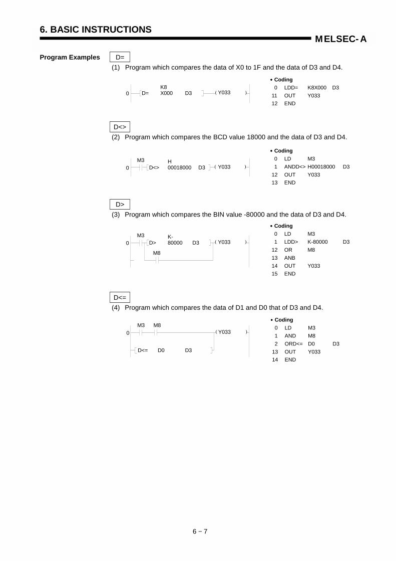
6. BASIC INSTRUCTIONS
6 − 7
MELSEC-A
Program Examples D=(1) Program which compares the data of X0 to 1F and the data of D3 and D4.
D<>(2) Program which compares the BCD value 18000 and the data of D3 and D4.
D>(3) Program which compares the BIN value -80000 and the data of D3 and D4.
D<=(4) Program which compares the data of D1 and D0 that of D3 and D4.
( )0K8
D= X000 D3 Y033
•••• Coding0 LDD= K8X000 D3
11 OUT Y03312 END
( )0H
D<> 00018000 D3 Y033
•••• Coding0 LD M31 ANDD<> H00018000 D3
12 OUT Y03313 END
M3
( )0K-
D> 80000 D3 Y033
•••• Coding0 LD M31 LDD> K-80000 D3
12 OR M813 ANB14 OUT Y03315 END
M3
M8
( )0
D<= D0 D3
Y033
•••• Coding0 LD M31 AND M82 ORD<= D0 D3
13 OUT Y03314 END
M3 M8
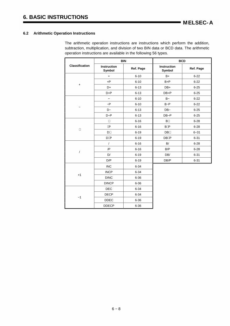
6. BASIC INSTRUCTIONS
6 − 8
MELSEC-A
6.2 Arithmetic Operation Instructions
The arithmetic operation instructions are instructions which perform the addition,subtraction, multiplication, and division of two BIN data or BCD data. The arithmeticoperation instructions are available in the following 56 types.
BIN BCDClassification Instruction
Symbol Ref. Page InstructionSymbol Ref. Page
+ 6-10 B+ 6-22
+P 6-10 B+P 6-22
D+ 6-13 DB+ 6-25+
D+P 6-13 DB+P 6-25
− 6-10 B− 6-22
−P 6-10 B−P 6-22
D− 6-13 DB− 6-25−
D−P 6-13 DB−P 6-25
∗ 6-16 B∗ 6-28
∗ P 6-16 B∗ P 6-28
D∗ 6-19 DB∗ 6−31∗
D∗ P 6-19 DB∗ P 6-31
/ 6-16 B/ 6-28
/P 6-16 B/P 6-28
D/ 6-19 DB/ 6-31/
D/P 6-19 DB/P 6-31
INC 6-34
INCP 6-34
DINC 6-36+1
DINCP 6-36
DEC 6-34
DECP 6-34
DDEC 6-36−1
DDECP 6-36

6. BASIC INSTRUCTIONS
6 − 9
MELSEC-A
Arithmetic operation with BIN (Binary)
• If the operation result of an addition instruction exceeds 32767 (2147483647 inthe case of a 32-bit instruction), the result becomes a negative value.
• If the operation result of a subtraction instruction is less than - 32768(-2147483648 in the case of a 32-bit instruction), the result becomes a positivevalue.
• The operation of a positive value and a negative value is as follows:
5 + 8 → 135 - 8 → -35 × 3 → 15
-5 × 3 → -15-5 × (−3) → 15-5 / 3 → -1 and remainder -25 / (−3) → -1 and remainder 2
-5 / (−3) → 1 and remainder -2
Arithmetic operation with BCD
• If the operation result of an addition instruction has exceeded 9999 (99999999 inthe case of a 32-bit instruction), carry is ignored.
• When the subtrahend is less than the minuend in the subtraction instruction, thefollowing occurs.
Carry is ignored.
99 9 9 9 0 0 0 1 1 0 0 0 0
0 0 0 5 0 0 0 81 9 9 9 7
Carry
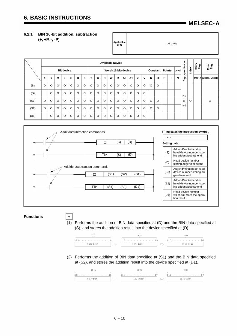
6. BASIC INSTRUCTIONS
6 − 10
MELSEC-A
6.2.1 BIN 16-bit addition, subtraction(+, +P, -, -P)
Available Device
Bit device Word (16-bit) device Constant Pointer Level Car
ryfla
g
Erro
rfla
g
X Y M L S B F T C D W R A0 A1 Z V K H P I N
Digi
t spe
cific
atio
n
Inde
x
M9012 (M9010, M9011)
(S) O O O O O O O O O O O O O O O O O O
(D) O O O O O O O O O O O O O O O
(S1) O O O O O O O O O O O O O O O O O O
(S2) O O O O O O O O O O O O O O O O O O
(D1) O O O O O O O O O O O O O O O
K1
to
K4
O O
Functions +(1) Performs the addition of BIN data specifies at (D) and the BIN data specified at
(S), and stores the addition result into the device specified at (D).
(2) Performs the addition of BIN data specified at (S1) and the BIN data specifiedat (S2), and stores the addition result into the device specified at (D1).
ApplicableCPU All CPUs
(S)Addend/subtrahend orhead device number stor-ing addend/subtrahend
(D) Head device numberstoring augend/minuend
(S1)Augend/minuend or headdevice number storing au-gend/minuend
(S2)Addend/subtrahend orhead device number stor-ing addend/subtrahend
(D1)Head device numberwhich will store the opera-tion result
Setting data
+, -
Indicates the instruction symbol.
b15 b0
(D)
5678(BIN) 1234(BIN)
b15 b0 b15 b0
6912(BIN)
(S) (D)
b15 b0
(S1)
5678(BIN) 1234(BIN)
b15 b0 b15 b0
6912(BIN)
(S2) (D1)
Addition/subtraction commands
Addition/subtraction commands
(S) (D)
(S) (D)
(S1) (S2) (D1)
(S1) (S2) (D1)
P
P

6. BASIC INSTRUCTIONS
6 − 11
MELSEC-A
(3) At (S), (S1), (S2) and (D), -32768 to 32767 (BIN 16 bits) can be specified.
(4) The judgment of whether the data of (S), (S1), (S2) and (D) are positive ornegative is made at the highest bit (b15).
0 ⋅⋅⋅⋅⋅⋅ Positive1 ⋅⋅⋅⋅⋅⋅ Negative
(5) When the 0th bit has underflown, the carry flag does not turn on.When the 15th bit has overflown, the carry flag does not turn on.
Functions -(1) Performs the subtraction of BIN data specified at (D) and the BIN data specified
at (S), and stores the subtraction result into the device specified at (D).
(2) Performs the subtraction of BIN data specified at (S1) and the BIN dataspecified at (S2), and stores the subtraction result into the device specified at(D1).
(3) At (S), (S1), (S2) and (D), -32768 to 32767 (BIN 16 bits) can be specified.
(4) The judgement of whether the dates of (S), (S1), (S2) and (D) are positive ornegative is made at the highest bit (b15).0 ……..Positive1 ……..Negative
(5) When the 0th bit has underflown, the carry flag does not turn on.When the 15th bit has overflown, the carry flag does not turn on.
b15 b0
(D)
5678(BIN) 1234(BIN)
b15 b0 b15 b0
4444(BIN)
(S) (D)
b15 b0
(S1)
5678(BIN) 1234(BIN)
b15 b0 b15 b0
4444(BIN)
(S2) (D1)

6. BASIC INSTRUCTIONS
6 − 12
MELSEC-A
Execution Conditions
Program Examples +Program which adds the content of A0 to the content of D3 and outputs the result toY38 to 3F when X5 turns on.
-Program which outputs the difference between the set value and present value timerT3 to Y40 to 53 in BCD.
• Coding0 LD X0051 +P D3 A0 K2Y0388 END
0X005 P K2
+ D3 A0 Y038
• Coding0 LD X0031 OUT T3 K180002 LD M90363 -P K18000 T3 D3
10 DBCD D3 K5Y04019 END
( )0
2
X003
M9036
K18000T3
P K- 18000 T3 D3
K5DBCD D3 Y040
OFF
ON
Addition/subtractioncommand
Executedper scan
Executedper scan
Executedonly once
Executedonly once
P
OFFON

MEMO

6. BASIC INSTRUCTIONS
6 − 13
MELSEC-A
6.2.2 BIN 32-bit addition, subtraction(D+, D+P, D-, D-P)
Available Device
Bit device Word (16-bit) device Constant Pointer Level Car
ryfla
g
Erro
rfla
g
X Y M L S B F T C D W R A0 A1 Z V K H P I N
Digi
t spe
cific
atio
n
Inde
x
M9012 (M9010, M9011)
(S) O O O O O O O O O O O O O O O O
(D) O O O O O O O O O O O O O
(S1) O O O O O O O O O O O O O O O O
(S2) O O O O O O O O O O O O O O O O
(D1) O O O O O O O O O O O O O
K1
to
K8
O O
Functions D+(1) Performs the addition of BIN data specified at (D) and the BIN data specified at
(S), and stores the addition result into the device specified at (D).
(2) Performs the addition of BIN data specified at (S1) and the BIN data specifiedat (S2), and stores the addition result into the device specified at (D1).
ApplicableCPU All CPUs
(S)Addend/subtrahend orhead device number stor-ing addend/subtrahend
(D) Head device numberstoring augend/minuend
(S1)Augend/minuend or headdevice number storing au-gend/minuend
(S2)Addend/subtrahend orhead device number stor-ing addend/subtrahend
(D1) Head device numberwhich will store the opera-tion result
Setting data
D+, D-
Indicates the instruction symbol.Addition/subtraction commands
Addition/subtraction commands
(S) (D)
(D)
(S1)
(S)
(S2) (D1)
(S1) (S2) (D1)
b31 b16
(D)+1
567890(BIN) 123456(BIN)
b0
691346(BIN)
(D)
b15 b31 b16
(S)+1
b0
(S)
b15 b31 b16
(D)+1
b0
(D)
b15
b31 b16
(S1)+1
567890(BIN) 123456(BIN)
b0
691346(BIN)
(S1)
b15 b31 b16
(S2)+1
b0
(S2)
b15 b31 b16
(D1)+1
b0
(D1)
b15
P
P
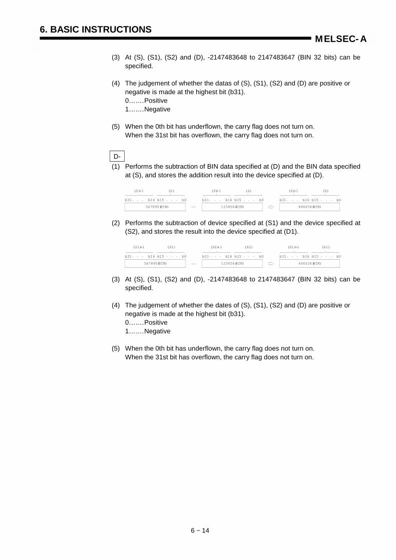
6. BASIC INSTRUCTIONS
6 − 14
MELSEC-A
(3) At (S), (S1), (S2) and (D), -2147483648 to 2147483647 (BIN 32 bits) can bespecified.
(4) The judgement of whether the datas of (S), (S1), (S2) and (D) are positive ornegative is made at the highest bit (b31).0…….Positive1…….Negative
(5) When the 0th bit has underflown, the carry flag does not turn on.When the 31st bit has overflown, the carry flag does not turn on.
D-(1) Performs the subtraction of BIN data specified at (D) and the BIN data specified
at (S), and stores the addition result into the device specified at (D).
(2) Performs the subtraction of device specified at (S1) and the device specified at(S2), and stores the result into the device specified at (D1).
(3) At (S), (S1), (S2) and (D), -2147483648 to 2147483647 (BIN 32 bits) can bespecified.
(4) The judgement of whether the dates of (S), (S1), (S2) and (D) are positive ornegative is made at the highest bit (b31).0…….Positive1…….Negative
(5) When the 0th bit has underflown, the carry flag does not turn on.When the 31st bit has overflown, the carry flag does not turn on.
b31 b16
(D)+1
567890(BIN) 123456(BIN)
b0
444434(BIN)
(D)
b15 b31 b16
(S)+1
b0
(S)
b15 b31 b16
(D)+1
b0
(D)
b15
b31 b16
(S1)+1
567890(BIN) 123456(BIN)
b0
444434(BIN)
(S1)
b15 b31 b16
(S2)+1
b0
(S2)
b15 b31 b16
(D1)+1
b0
(D1)
b15
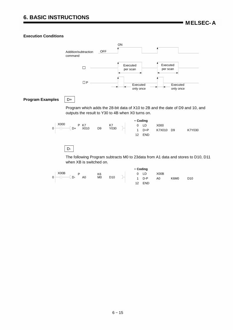
6. BASIC INSTRUCTIONS
6 − 15
MELSEC-A
Execution Conditions
Program Examples D+
Program which adds the 28-bit data of X10 to 2B and the date of D9 and 10, and outputs the result to Y30 to 4B when X0 turns on.
D-
The following Program subtracts M0 to 23data from A1 data and stores to D10, D11 when XB is switched on.
Addition/subtractioncommand
Executedper scan
Executedper scan
Executedonly once
• Coding0 LD X0001 D+P K7X010 D9 K7Y030
12 END
0X000 P K7 K7
D+ X010 D9 Y030
• Coding0 LD X00B1 D-P A0 K6M0 D10
12 END
0X00B P K6
D- A0 M0 D10
P
ON
OFF
Executedonly once

MEMO

6. BASIC INSTRUCTIONS
6 − 16
MELSEC-A
6.2.3 BIN 16-bit multiplication, division(*, *P, /, /P)
Available Device
Bit device Word (16-bit) device Constant Pointer Level Car
ryfla
g
Erro
rfla
g
X Y M L S B F T C D W R A0 A1 Z V K H P I N
Digi
t spe
cific
atio
n
Inde
x
M9012 (M9010, M9011)
(S1) O O O O O O O O O O O O O O O O O O
(S2) O O O O O O O O O O O O O O O O O O
(D) O O O O O O O O O O O O O
K1
to
K4
O O
Functions *(1) Performs the multiplication of BIN data specified at (S1) and the BIN data
specified at (S2), and stores the multiplication result into the device specified at(D).
(2) When (D) is a bit device, specify the bits, beginning with the lower bits.Example
K1: Lower 4 bits (b0 to 3)K4: Lower 16 bits (b0 to 15)K8: 32 bits (b0 to 31)
(3) At (S1) and (S2), -32768 to 32767 (BIN 16 bits) can be specified.
(4) The judgment of whether the data of (S1) and (S2) are positive or negative ismade at the highest bit (b15) and that of (D), at (b31).
ApplicableCPU All CPUs
(S1)Multiplicand/dividend orhead device numberstoring multiplier/dividend
(S2)Multiplicand/divider orhead device numberstoring multiplier/divider
(D) Head device numberwhich will store the result
Setting data
∗ , /
Indicates the instruction symbol.Multiplication/division commands
(D)(S1)
(S1) (S2)
(S2)
(D)
P
b15 b0
(S1)
5678(BIN) 1234(BIN)
b15 b0
7006652(BIN)
(S2)
b31 b16
(D)+1
b0
(D)
b15
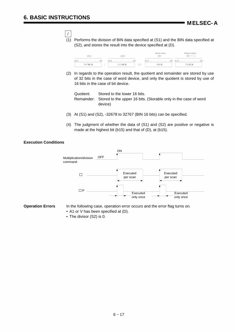
6. BASIC INSTRUCTIONS
6 − 17
MELSEC-A
/(1) Performs the division of BIN data specified at (S1) and the BIN data specified at
(S2), and stores the result into the device specified at (D).
(2) In regards to the operation result, the quotient and remainder are stored by useof 32 bits in the case of word device, and only the quotient is stored by use of16 bits in the case of bit device.
Quotient: Stored to the lower 16 bits.Remainder: Stored to the upper 16 bits. (Storable only in the case of word
device)
(3) At (S1) and (S2), -32678 to 32767 (BIN 16 bits) can be specified.
(4) The judgment of whether the data of (S1) and (S2) are positive or negative ismade at the highest bit (b15) and that of (D), at (b15).
Execution Conditions
Operation Errors In the following case, operation error occurs and the error flag turns on.• A1 or V has been specified at (D).• The divisor (S2) is 0.
b15 b0
(S2)
1234( BIN)
b15 b0
Quotient(D)
b15 b0
742( BIN)
b15 b0
(S1)
5678 (BIN)
Remainder(D) + 1
4( BIN)
Multiplication/divisioncommand
Executedper scan
Executedper scan
Executedonly once
P
ON
OFF
Executedonly once
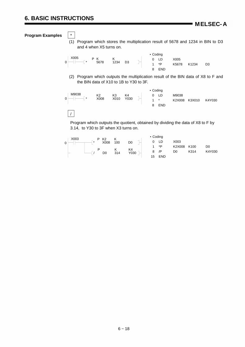
6. BASIC INSTRUCTIONS
6 − 18
MELSEC-A
Program Examples *(1) Program which stores the multiplication result of 5678 and 1234 in BIN to D3
and 4 when X5 turns on.
(2) Program which outputs the multiplication result of the BIN data of X8 to F andthe BIN data of X10 to 1B to Y30 to 3F.
/
Program which outputs the quotient, obtained by dividing the data of X8 to F by 3.14, to Y30 to 3F when X3 turns on.
• Coding0 LD X0051 *P K5678 K1234 D38 END
0X005 P K K
* 5678 1234 D3
• Coding0 LD M90381 * K2X008 K3X010 K4Y0308 END
0M9038 K2 K3 K4
* X008 X010 Y030
• Coding0 LD X0031 *P K2X008 K100 D08 /P D0 K314 K4Y030
15 END
0X003 P K2 K
* X008 100 D0
P K K4/ D0 314 Y030

MEMO

6. BASIC INSTRUCTIONS
6 − 19
MELSEC-A
6.2.4 BIN 32-bit multiplication, division(D*, D*P, D/, D/P)
Available Device
Bit device Word (16-bit) device Constant Pointer Level Car
ryfla
g
Erro
rfla
g
X Y M L S B F T C D W R A0 A1 Z V K H P I N
Digi
t spe
cific
atio
n
Inde
x
M9012 (M9010, M9011)
(S1) O O O O O O O O O O O O O O O O
(S2) O O O O O O O O O O O O O O O O
(D) O O O O O O O O O O O
K1toK8
O O
Functions D*(1) Performs the multiplication of BIN data specified at (S1) and the BIN data speci-
fied at (S2), and stores the multiplication result into the device specified at (D).
(2) When (D) is a bit device, up to the lower 32 bits can be specified and the upper32 bits cannot be specified.Example
K1: Lower 4 bits (b0 to 3)K4: Lower 16 bits (b0 to 15)K8: 32 bits (b0 to 31)
When the upper 32-bit data of multiplication result is required for the bit device,store the data to the word device and then transfer the data ((D)+2) and ((D)+3)of word device to the specified bit device.
(3) At (S1) and (S2), -2147483648 to 2147483647 (BIN 32 bits) can be specified.
(4) The judgment of whether the data of (S1) and (S2) are positive or negative ismade at the highest bit (b31) and that of (D), at (b63).
ApplicableCPU All CPUs
b31 b16
(S1)+1 (S1)
b15 b31 b16
(S2)+1 (S2)
b15b0 b0
(D)+3 (D)+2 (D)+1 (D)
b63 b47 b31 b15
b48 b32 b16 b0
567890(BIN) 123456(BIN) 70109427840(BIN)
(S1)Multiplicand/dividend orhead device numberstoring multiplier/dividend
(S2)Multiplicand/divider orhead device numberstoring multiplier/divider
(D)Head device numberwhich will store theresult
Setting data
D*, D/
Indicates the instruction symbol.Multiplication/division commands
(S1) (S2) (D)
(D)(S2)(S1)P

6. BASIC INSTRUCTIONS
6 − 20
MELSEC-A
D/(1) Performs the division of BIN data specified at (S1) and the BIN data specified at
(S2), and stores the division result into the device specified at (D).
(2) In regards to the operation result, the quotient and remainder are stored by useof 64 bits in the case of word device, and only the quotient is stored by use oflower 32 bits in the case of bit device.
Quotient: Stored to the lower 32 bits.Remainder: Stored to the upper 32 bits. (Storable only in the case of word
device)
(3) At (S1) and (S2), -2147483648 to 2147483647 (BIN 32 bits) can be specified.
(4) The judgment of whether the data of (S1), (S2), (D) and (D+2) are positive ornegative is made at the highest bit (b31).
Execution Conditions
Operation Errors In the following case, operation error occurs and the error flag turns on.• A1, V are specified in (S1), (S2) and A0, A1, Z, V specified in (D).• The divisor (S2) is 0.
74066( BIN)4(BIN)567890(BIN)
b31 b16
(S1)+1 (S1)
b15 b0
123456(BIN)
b31 b16
(S2)+1 (S2)
b15 b0
b31
(D)+1 (D)
b15 b31
(D)+3
b15
Quotient Remainder
b16 b0 b16 b0
(D)+2
OFF
ON
Executedper scan
Executedper scan
Executedonly once
Executedonly once
P
Multiplication/divisioncommand

6. BASIC INSTRUCTIONS
6 − 21
MELSEC-A
Program Examples D*Program which stores the multiplication result of the BIN data of D7 and D8 and theBIN data of D18 and D19 to D1 to D4 when X5 turns on.
D/Program which outputs a value, obtained by multiplying the data of X8 to F by 3.14,to Y30 to 3F when X3 turns on.
X005D* D7 D18 D10
P • Coding0 LD X0051 D*P D7 D18 D1
12 END
• Coding0 LD X0031 *P K2X008 K314 D08 D/P D0 K100 D2
19 MOVP D2 K4Y03024 ENDMOV D2 Y030
* X008 314 D0
D/ D0 100 D2
P K2 K
P
P K4
0X003
K

MEMO

6. BASIC INSTRUCTIONS
6 − 22
MELSEC-A
6.2.5 BCD 4-digit addition, subtraction(B+, B+P, B-, B-P)
Available Device
Bit device Word (16-bit) device Constant Pointer Level Car
ryfla
g
Erro
rfla
g
X Y M L S B F T C D W R A0 A1 Z V K H P I N
Digi
t spe
cific
atio
n
Inde
x
M9012 (M9010, M9011)
(S) O O O O O O O O O O O O O O O O O O
(D) O O O O O O O O O O O O O O O
(S1) O O O O O O O O O O O O O O O O O O
(S2) O O O O O O O O O O O O O O O O O O
(D1) O O O O O O O O O O O O O O O
K1
to
K4
O O
Functions B+(1) Performs the addition of BCD data specified at (D) and the BCD data specified
at (S), and stores the addition result into the device specified at (D).
(2) Performs the addition of BCD data specified at (S1) and the BCD data specifiedat (S2), and stores the addition result into the device specified at (D1).
(3) At (S), (S1), (S2) and (D), 0 to 9999 (BCD 4 digits) can be specified.
(4) Even if the addition result exceeds 9999, the carry flag does not turn on and thecarry digit is ignored.
ApplicableCPU All CPUs
(S) (D)
(S) (D)P
Addition/subtraction commands
(S)Addend/subtrahend orhead device number stor-ing addend/subtrahend
(D) Head device numberstoring augend/minuend
(S1)Augend/minuend or headdevice number storing au-gend/minuend
(S2)Addend/subtrahend orhead device number stor-ing addend/subtrahend
(D1)Head device numberwhich will store theoperation result
Setting data
B+, B-
Indicates the instruction symbol.
Addition/subtraction commands
(S1) (D1)
(S1) (D1)P
(S2)
(S2)
(D)
5 6 7 8
(S) (D)
1 2 3 4 6 9 1 2
(S1)
5 6 7 8
(S2) (D1)
1 2 3 4 6 9 1 2

6. BASIC INSTRUCTIONS
6 − 23
MELSEC-A
B-(1) Performs the subtraction of BCD data specified at (D) and the BCD data specifi-
ed at (S), and stores the subtraction result into the device specified at (D).
(2) Performs the subtraction of BCD data specified at (S2) and the BCD data speci-fied at (S1), and stores the subtraction result into the device specified at (D1).
(3) At (S), (S1), (S2) and (D), 0 to 9999 (BCD 4 digits) can be specified.
(4) It is required to judge whether the operation result is positive or negative by useof the program.
Execution Conditions
Operation Errors In the following cases, operation error occurs and the error flag turns on.• A value other than 0 to 9 exists in any digit of (S) (S1), (S2), (D).
(D)
0 6 7 8
(S) (D)
0 2 3 4 0 4 4 4
Digit higher than the specified digit is regarded as 0.
(S1)
0 6 7 8
(S2) (D1)
0 2 3 4 0 4 4 4
Digit higher than the specified digit is regarded as 0.
OFF
ON
Executedper scan
Executedper scan
Executedonly once
Executedonly once
P
Addition/subtractioncommands

6. BASIC INSTRUCTIONS
6 − 24
MELSEC-A
Program Examples B+Program which performs the addition of BCD data 5678 and 1234, and stores theresult to D993, and at the same time outputs it to Y30 to 3F.
B-Program which performs subtraction of the BCD data of D3 and that of D8 andtransfers the result to M16 to 31 when X1B turns on.
•••• Coding0 LD M90361 MOVP H5678 D9936 B+P H1234 D993
13 MOVP D993 K4Y03018 END
0M9036
P HB+ 1234 D993
P HMOV 5678 D993
P K4MOV D993 Y030
5678 is stored into D993 in BCD
BCD data 1234 and D993 are added and theresult is stored into D993.
Data of D993 is output to the Y30 to 3F.
0X01B P K4
B- D3 D8 M16
•••• Coding0 LD X01B1 B-P D3 D8 K4M16
10 END

MEMO
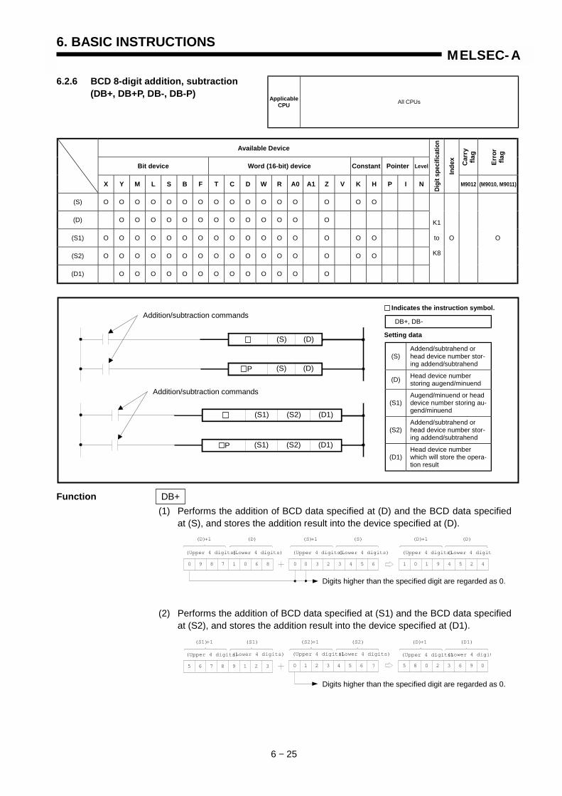
6. BASIC INSTRUCTIONS
6 − 25
MELSEC-A
6.2.6 BCD 8-digit addition, subtraction(DB+, DB+P, DB-, DB-P)
Available Device
Bit device Word (16-bit) device Constant Pointer Level Car
ryfla
g
Erro
rfla
g
X Y M L S B F T C D W R A0 A1 Z V K H P I N
Digi
t spe
cific
atio
n
Inde
x
M9012 (M9010, M9011)
(S) O O O O O O O O O O O O O O O O
(D) O O O O O O O O O O O O O
(S1) O O O O O O O O O O O O O O O O
(S2) O O O O O O O O O O O O O O O O
(D1) O O O O O O O O O O O O O
K1
to
K8
O O
Function DB+(1) Performs the addition of BCD data specified at (D) and the BCD data specified
at (S), and stores the addition result into the device specified at (D).
(2) Performs the addition of BCD data specified at (S1) and the BCD data specifiedat (S2), and stores the addition result into the device specified at (D1).
ApplicableCPU All CPUs
(S) (D)
(S) (D)P
Addition/subtraction commands
(S)Addend/subtrahend orhead device number stor-ing addend/subtrahend
(D) Head device numberstoring augend/minuend
(S1)Augend/minuend or headdevice number storing au-gend/minuend
(S2)Addend/subtrahend orhead device number stor-ing addend/subtrahend
(D1)Head device numberwhich will store the opera-tion result
Setting data
DB+, DB-
Indicates the instruction symbol.
Addition/subtraction commands
(S1) (D1)
(S1) (D1)P
(S2)
(S2)
0 9 8 7 1 0 6 8 0 0 3 2 3 4 5 6 1 0 1 9 4 5 2 4
(D)+1 (D) (S)+1 (S) (D)+1 (D)
(Upper 4 digits) (Upper 4 digits) (Upper 4 digits)(Lower 4 digits) (Lower 4 digits) (Lower 4 digit
Digits higher than the specified digit are regarded as 0.
5 6 7 8 9 1 2 3 0 1 2 3 4 5 6 5 8 0 2 3 6 9 0
(S1)+1 (S1) (S2)+1 (S2) (D)+1 (D1)
(Upper 4 digits) (Upper 4 digits) (Upper 4 digits)(Lower 4 digits) (Lower 4 digits) (Lower 4 digit
7
Digits higher than the specified digit are regarded as 0.

6. BASIC INSTRUCTIONS
6 − 26
MELSEC-A
(3) At (S), (S1), (S2) and D, 0 to 99999999 (BCD 8 digits) can be specified.
(4) Even if the addition result exceeds 99999999, the carry flag does not turn onand the carry digit is ignored.
DB-(1) Subtracts the BCD data specified at (S) from the BCD data specified at (D), and
stores the subtraction result into the device specified at (D).
(2) Performs subtraction of the BCD data specified at (S1) and the BCD data speci-fied at (S2), and stores the subtraction result into the device specified at (D1).
(3) At (S), (S1), (S2) and (D), 0 to 99999999 (BCD 8 digits) can be specified.
(4) It is required to judge whether the operation result is positive or negative by useof the program.
Execution Conditions
5 6 7 8 9 1 2 3 0 1 2 3 4 5 6 5 5 5 5 4 5 5 6
(S1)+1 (S1) (S2)+1 (S2) (D)+1 (D1)
(Upper 4 digits) (Upper 4 digits) (Upper 4 digits)(Lower 4 digits) (Lower 4 digits) (Lower 4 digit
7
0 9 8 7 1 0 6 8 0 0 3 2 3 4 5 6 0 9 5 4 7 6 1 2
(D)+1 (D) (S)+1 (S) (D)+1 (D)
(Upper 4 digits) (Upper 4 digits) (Upper 4 digits)(Lower 4 digits) (Lower 4 digits) (Lower 4 digit
Digits higher than the specified digit are regarded as 0.
Digits higher than the specified digit are regarded as 0.
OFF
ON
Executedper scan
Executedper scan
Executedonly once
Executedonly once
P
Addition/subtractioncommands
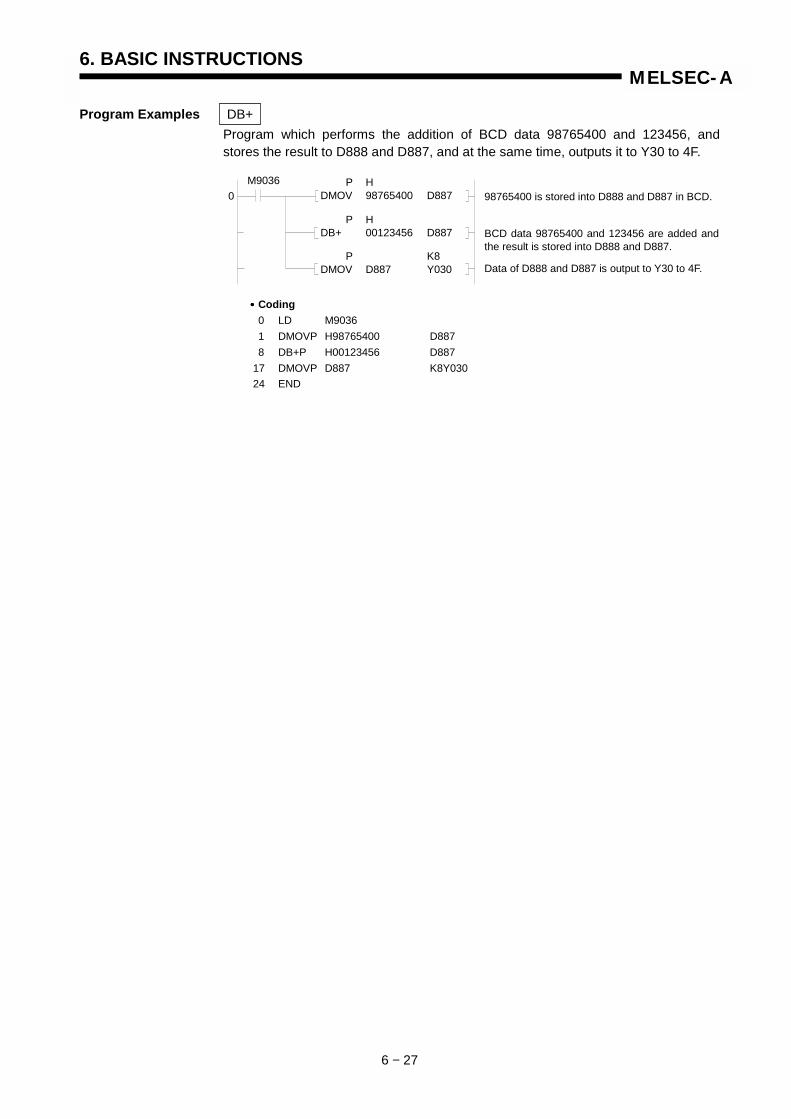
6. BASIC INSTRUCTIONS
6 − 27
MELSEC-A
Program Examples DB+Program which performs the addition of BCD data 98765400 and 123456, andstores the result to D888 and D887, and at the same time, outputs it to Y30 to 4F.
•••• Coding0 LD M90361 DMOVP H98765400 D8878 DB+P H00123456 D887
17 DMOVP D887 K8Y03024 END
0M9036
P HDB+ 00123456 D887
P HDMOV 98765400 D887
P K8DMOV D887 Y030
98765400 is stored into D888 and D887 in BCD.
BCD data 98765400 and 123456 are added andthe result is stored into D888 and D887.
Data of D888 and D887 is output to Y30 to 4F.

MEMO
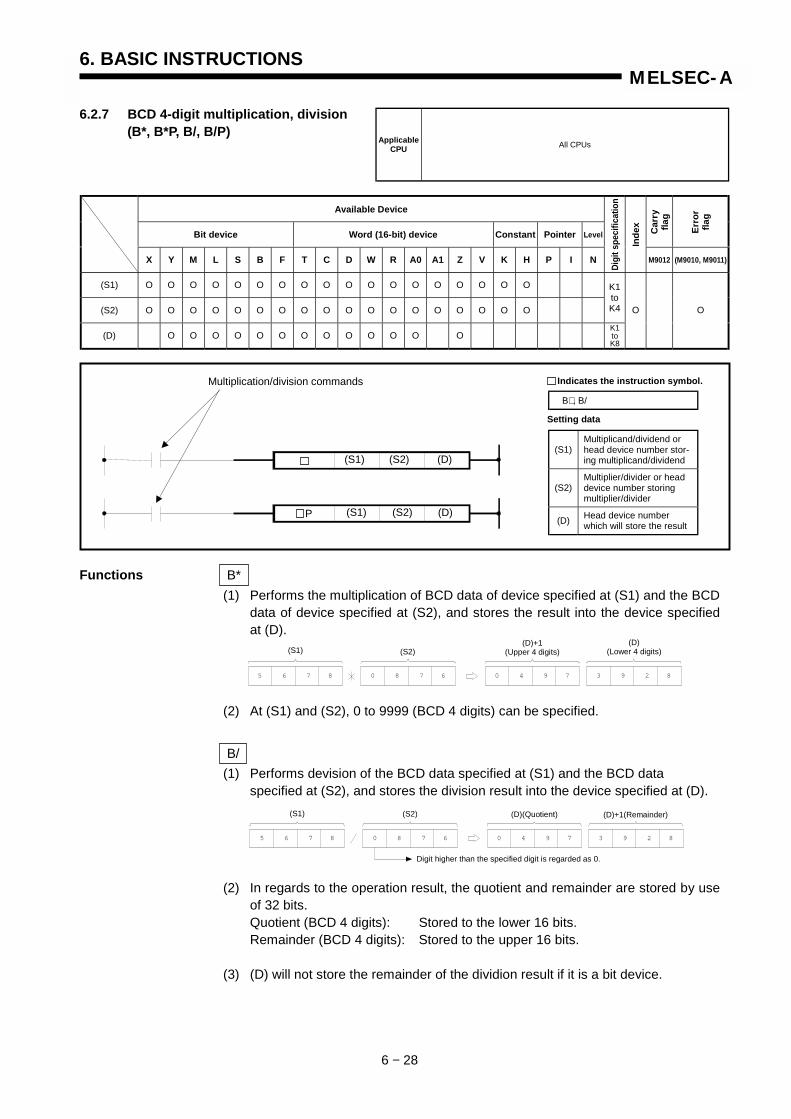
6. BASIC INSTRUCTIONS
6 − 28
MELSEC-A
6.2.7 BCD 4-digit multiplication, division(B*, B*P, B/, B/P)
Available Device
Bit device Word (16-bit) device Constant Pointer Level Car
ryfla
g
Erro
rfla
g
X Y M L S B F T C D W R A0 A1 Z V K H P I N
Digi
t spe
cific
atio
n
Inde
x
M9012 (M9010, M9011)
(S1) O O O O O O O O O O O O O O O O O O
(S2) O O O O O O O O O O O O O O O O O O
K1toK4
(D) O O O O O O O O O O O O O
O O
Functions B*(1) Performs the multiplication of BCD data of device specified at (S1) and the BCD
data of device specified at (S2), and stores the result into the device specifiedat (D).
(2) At (S1) and (S2), 0 to 9999 (BCD 4 digits) can be specified.
B/(1) Performs devision of the BCD data specified at (S1) and the BCD data
specified at (S2), and stores the division result into the device specified at (D).
(2) In regards to the operation result, the quotient and remainder are stored by useof 32 bits.Quotient (BCD 4 digits): Stored to the lower 16 bits.Remainder (BCD 4 digits): Stored to the upper 16 bits.
(3) (D) will not store the remainder of the dividion result if it is a bit device.
ApplicableCPU All CPUs
K1toK8
0 8 7 6 0 4 9 7 3 9 2 85 6 7 8
(S1) (S2)(D)+1
(Upper 4 digits)(D)
(Lower 4 digits)
0 8 7 6 0 4 9 7 3 9 2 85 6 7 8
(S1) (S2) (D)(Quotient) (D)+1(Remainder)
Digit higher than the specified digit is regarded as 0.
Multiplication/division commands
(S1) (S2) (D)
(S1) (S2) (D)P
(S1)Multiplicand/dividend orhead device number stor-ing multiplicand/dividend
(S2)Multiplier/divider or headdevice number storingmultiplier/divider
(D) Head device numberwhich will store the result
Setting data
B∗ , B/
Indicates the instruction symbol.

6. BASIC INSTRUCTIONS
6 − 29
MELSEC-A
Execution Conditions
Operation Errors In the following cases, operation error occurs and the error flag turns on.• A value other than 0 to 9 exists in any digit of (S1), (S2).• The divisor (S2) is 0.
Program Examples B*Program which performs multiplication of the BCD data of X0 to F and BCD data ofD8, and stores the result into A0 and A1 when X1B turns on.
• Coding0 LD X01B1 B*P K4X000 D8 A0
10 END
0X01B P K4
B* X000 D8 A0
D8 A1(Upper 4 digits)
8 6 4 2 8 4 2 8 5 4 2 69 5 3
A0(Lower 4 digits)
Multiplicand
XF X0
7
Multiplier Multiplication result
OFF
ON
Multiplication/divisioncommands
Executedper scan
Executedper scan
Executedonly once
Executedonly once
P
OFFON
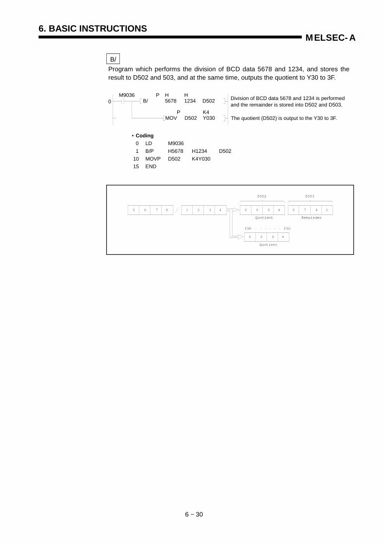
6. BASIC INSTRUCTIONS
6 − 30
MELSEC-A
B/Program which performs the division of BCD data 5678 and 1234, and stores theresult to D502 and 503, and at the same time, outputs the quotient to Y30 to 3F.
Division of BCD data 5678 and 1234 is performedand the remainder is stored into D502 and D503.
P H HB/ 5678 1234 D502
P K4MOV D502 Y030
0M9036
The quotient (D502) is output to the Y30 to 3F.
• Coding0 LD M90361 B/P H5678 H1234 D502
10 MOVP D502 K4Y03015 END
D502
1 2 3 4 0 0 0 4 0 7 4 25 7 8
D503
Y3F Y3O
6
Quotient
0 0 0 4
Remainder
Quotient

MEMO

6. BASIC INSTRUCTIONS
6 − 31
MELSEC-A
6.2.8 BCD 8-digit multiplication, division(DB*, DB*P, DB/, DB/P)
Available Device
Bit device Word (16-bit) device Constant Pointer Level Car
ryfla
g
Erro
rfla
g
X Y M L S B F T C D W R A0 A1 Z V K H P I N
Digi
t spe
cific
atio
n
Inde
x
M9012 (M9010, M9011)
(S1) O O O O O O O O O O O O O O O O
(S2) O O O O O O O O O O O O O O O O
(D) O O O O O O O O O O O
K1
to
K8
O O
Function DB*(1) Performs multiplication of the BCD data specified at (S1) and the BCD data
specified at (S2), and stores the multiplication result into the device specified at(D).
(2) If (D) is a bit device, the 8 lower digits (32 lower bits) of the multiplication resultmay only be specified.K1 1 lower digit (B0 to 3), K4 4 lower digits (B0 to 15), K8 8 lower digits (B0 to31)
(3) At (S1) and (S2), 0 to 99999999 (BCD 8 digits) can be specified.
ApplicableCPU All CPUs
(S1)+1 (S1)
99 9 999 9 9 99 9 9 99 9 9
(S2)+1 (S2)
(D)+3 (D)+2 (D)+1 (D)
89 9 999 9 9 00 0 0 10 0 0
Multiplication/division commands
(S1) (S2) (D)
(S1) (S2) (D)P
(S1)Multiplicand/dividend orhead device number stor-ing multiplicand/dividend
(S2)Multiplier/divider or headdevice number storingmultiplier/divider
(D) Head device numberwhich will store the result
Setting data
DB∗ , DB/
Indicates the instruction symbol.

6. BASIC INSTRUCTIONS
6 − 32
MELSEC-A
DB/(1) Performs division of the BCD data specified at (S1) and the BCD data specified
at (S2), and stores the division result into the device specified at (D).
(2) In regards to the operation result, the quotient and remainder are stored by useof 64 bits.Quotient (BCD 8 digits): Stored to the lower 32 bits.Remainder (BCD 8 digits): Stored to the upper 32 bits.
(3) (D) will not store the remainder of the division result if it is a bit device.
Execution Conditions
Operation Errors In the following cases, operation errors and the error flag turns on.• A value other than 0 to 9 exists in any digit of (S1), (S2).• The divisor (S2) is 0.
(D1)+1(Upper 4 digits)
(D)(Lower 4 digits)
(D)+3(Upper 4 digits)
(D)+2(Lower 4 digits)
50 0 400 0 0 30 1 2 83 6 0
Quotient Remainder
(S1)+1 (S1) (S2)+1 (S2)
39 1 285 6 7 30 1 2 74 5 6
Digit higher than the specified digit is regarded as 0.
OFF
ON
Multiplication/divisioncommands
Executedper scan
Executedper scan
Executedonly once
Executedonly once
P
OFFON
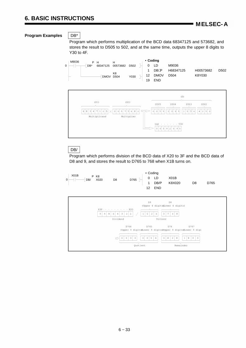
6. BASIC INSTRUCTIONS
6 − 33
MELSEC-A
Program Examples DB*Program which performs multiplication of the BCD data 68347125 and 573682, andstores the result to D505 to 502, and at the same time, outputs the upper 8 digits toY30 to 4F.
DB/Program which performs division of the BCD data of X20 to 3F and the BCD data ofD8 and 9, and stores the result to D765 to 768 when X1B turns on.
0 0 5 6
9
7 22
D505
Y4F Y3O
6 8 4 7 13 5
D504 D503 D502
83
0 0 3 2 0 9 5
90 0 3 2 0 9 5 61 5 3 4 2 5 0
(S1) (S2)
(D)
Multiplicand Multiplier
M90360
P H HDB* 68347125 00573682 D502
K8DMOV D504 Y030
• Coding0 LD M90361 DB∗ P H68347125 H00573682 D502
12 DMOV D504 K8Y03019 END
P K8DB/ X020 D8 D765
X01B0
• Coding0 LD X01B1 DB/P K8X020 D8 D765
12 END
0
6
2
2
X3F X2O
6 8
4 71
3
(Upper 4 digits)
8
3 61 5
D766
9
0 0
329
1
4
(Upper 4 digits)
(Upper 4 digits)(Lower 4 digits)
(Lower 4 digits)
(Lower 4 digi
D765 D76 D767
D9 D8
0 0 0 0 0 8 3
8 8
Dividend Divisor
Quotient Remainder

MEMO
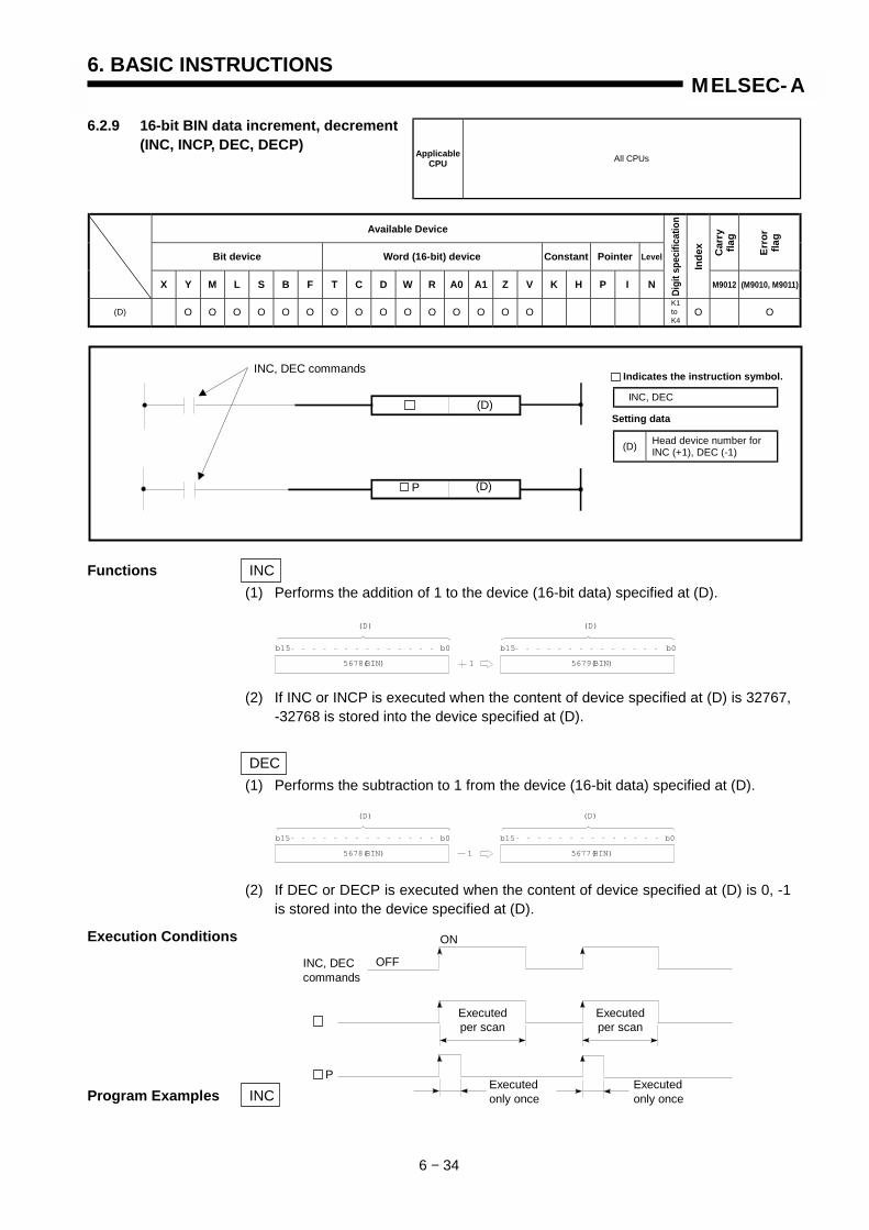
6. BASIC INSTRUCTIONS
6 − 34
MELSEC-A
6.2.9 16-bit BIN data increment, decrement(INC, INCP, DEC, DECP)
Available Device
Bit device Word (16-bit) device Constant Pointer Level Car
ryfla
g
Erro
rfla
g
X Y M L S B F T C D W R A0 A1 Z V K H P I N
Digi
t spe
cific
atio
n
Inde
x
M9012 (M9010, M9011)
(D) O O O O O O O O O O O O O O O O O
Functions INC(1) Performs the addition of 1 to the device (16-bit data) specified at (D).
(2) If INC or INCP is executed when the content of device specified at (D) is 32767,-32768 is stored into the device specified at (D).
DEC(1) Performs the subtraction to 1 from the device (16-bit data) specified at (D).
(2) If DEC or DECP is executed when the content of device specified at (D) is 0, -1is stored into the device specified at (D).
Execution Conditions
Program Examples INC
ApplicableCPU All CPUs
INC, DEC commands
K1toK4
(D)
(D)
(D) Head device number forINC (+1), DEC (-1)
Setting data
INC, DEC
Indicates the instruction symbol.
b15 b0
(D)
5678(BIN) 1
b15 b0
(D)
5679(BIN)
b15 b0
(D)
5678(BIN) 1
b15 b0
(D)
5677(BIN)
INC, DECcommands
Executedper scan
Executedper scan
Executedonly once
P
P
ON
OFF
Executedonly once
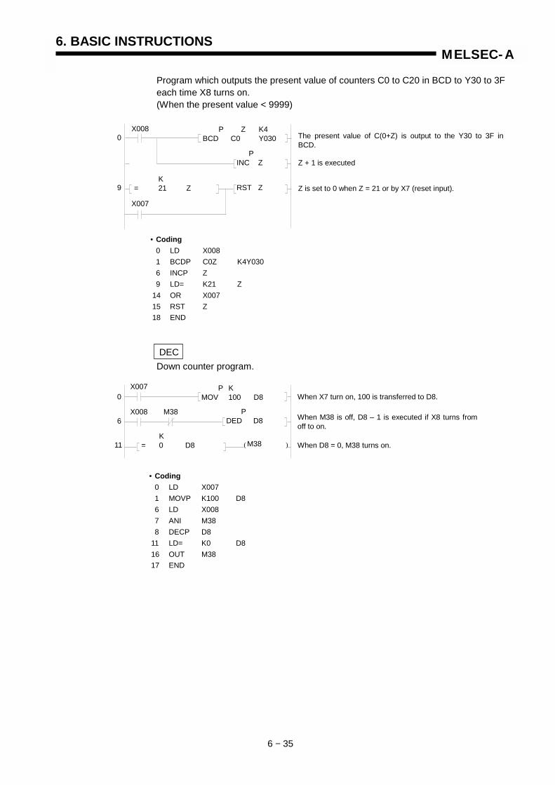
6. BASIC INSTRUCTIONS
6 − 35
MELSEC-A
Program which outputs the present value of counters C0 to C20 in BCD to Y30 to 3Feach time X8 turns on.(When the present value < 9999)
DECDown counter program.
The present value of C(0+Z) is output to the Y30 to 3F inBCD.
X008 P Z K4BCD C0 Y0300
PINC Z Z + 1 is executed
K= 21 Z9 Z is set to 0 when Z = 21 or by X7 (reset input).
X007
• Coding0 LD X0081 BCDP C0Z K4Y0306 INCP Z9 LD= K21 Z
14 OR X00715 RST Z18 END
RST Z
( )
X0070
6
P KMOV 100 D8 When X7 turn on, 100 is transferred to D8.
X008
11
M38 PDED D8
K= 0 D8
When M38 is off, D8 – 1 is executed if X8 turns fromoff to on.
M38 When D8 = 0, M38 turns on.
• Coding0 LD X0071 MOVP K100 D86 LD X0087 ANI M388 DECP D8
11 LD= K0 D816 OUT M3817 END
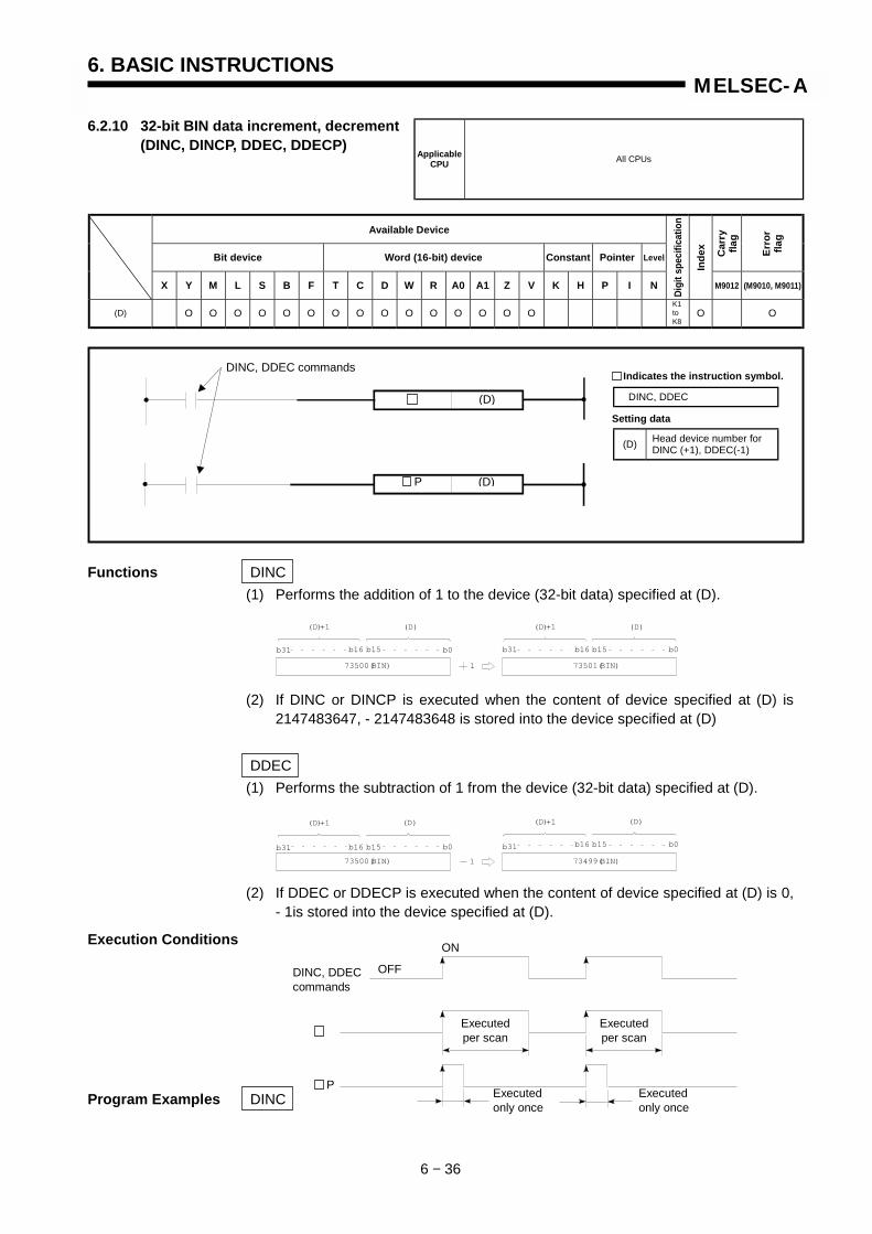
6. BASIC INSTRUCTIONS
6 − 36
MELSEC-A
6.2.10 32-bit BIN data increment, decrement(DINC, DINCP, DDEC, DDECP)
Available Device
Bit device Word (16-bit) device Constant Pointer Level Car
ryfla
g
Erro
rfla
g
X Y M L S B F T C D W R A0 A1 Z V K H P I N
Digi
t spe
cific
atio
n
Inde
x
M9012 (M9010, M9011)
(D) O O O O O O O O O O O O O O O O O
Functions DINC(1) Performs the addition of 1 to the device (32-bit data) specified at (D).
(2) If DINC or DINCP is executed when the content of device specified at (D) is2147483647, - 2147483648 is stored into the device specified at (D)
DDEC(1) Performs the subtraction of 1 from the device (32-bit data) specified at (D).
(2) If DDEC or DDECP is executed when the content of device specified at (D) is 0,- 1is stored into the device specified at (D).
Execution Conditions
Program Examples DINC
ApplicableCPU All CPUs
K1toK8
DINC, DDEC commands
(D)
(D)
(D) Head device number forDINC (+1), DDEC(-1)
Setting data
DINC, DDEC
Indicates the instruction symbol.
b31 b0
(D)
73500(BIN) 1 73501(BIN)
b16 b15
(D)+1
b31 b0
(D)
b16 b15
(D)+1
b31 b0
(D)
73500(BIN) 73499(BIN)
b16 b15
(D)+1
b31 b0
(D)
b16 b15
(D)+1
1
DINC, DDECcommands
Executedper scan
Executedper scan
Executedonly once
P
PExecutedonly once
ON
OFF

6. BASIC INSTRUCTIONS
6 − 37
MELSEC-A
(1) Program which adds 1 to the data of D0 and 1when X0 turns on.
(2) Program which adds 1 to the data of X10 to 27 and stores the result to D3 and4 when X0 turns on.
DDEC(1) Program which subtracts 1 from the data of D0 and 1 when X0 turns on.
(2) Program which subtracts 1 from the data of X10 to 27 and stores the result toD3 and 4 when X0 turns on.
X0000
PDINC DO
• Coding0 LD X0001 DINCP D04 END
• Coding0 LD X0001 DMOVP K6X010 D38 DINCP D3
11 END
X0000
P K6DMOV X010 D3
PDINC D3
X0000
PDDEC D0
• Coding0 LD X0001 DDECP D04 END
• Coding0 LD X0001 DMOVP K6X010 D38 DDECP D3
11 END
X0000
P K6DMOV X010 D3
PDDEC D3

6. BASIC INSTRUCTIONS
6 − 38
MELSEC-A
6.3 BCD ↔↔↔↔ BIN Conversion Instructions
The BCD ↔ BIN conversion instructions are instructions which convert BCD data toBIN data and BCD data.
Classification InstructionSymbol Ref. Page Classification Instruction
symbol Ref. Page
BCD 6-39 BIN 6-42
BCDP 6-39 BINP 6-42
DBCD 6-39 DBIN 6-42BDC
DBCDP 6-39
BIN
DBINP 6-42
Numeric values usable for the BCD ↔ BIN conversion instructions are as follows:
BCD, BCDP, BIN, BINP: 0 to 9999DBCD, DBCDP, DBIN, DBINP: 0 to 99999999

MEMO
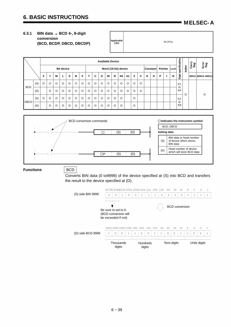
6. BASIC INSTRUCTIONS
6 − 39
MELSEC-A
6.3.1 BIN data →→→→ BCD 4-, 8-digitconversion(BCD, BCDP, DBCD, DBCDP)
Available Device
Bit device Word (16-bit) device Constant Pointer Level Car
ryfla
g
Erro
rfla
g
X Y M L S B F T C D W R A0 A1 Z V K H P I N
Digi
t spe
cific
atio
n
Inde
x
M9012 (M9010, M9011)
(S) O O O O O O O O O O O O O O O OBCD
(D) O O O O O O O O O O O O O O O
K1toK4
(S) O O O O O O O O O O O O O ODBCD
(D) O O O O O O O O O O O O O
K1toK8
O O
Functions BCDConverts BIN data (0 to9999) of the device specified at (S) into BCD and transfersthe result to the device specified at (D).
ApplicableCPU All CPUs
(S) (D)
(S) (D)P
BCD conversion commands
(S)BIN data or head numberof device which storesBIN data
(D) Head number of devicewhich will store BCD data
Setting data
BCD, DBCD
Indicates the instruction symbol.
32768163848192 4096
0 0 1 0 0 1 1 1 0 0 0 0 1 1 1 1
2048 1024 512 256 128 64 32 16 8 4 2 1
8000 4000 2000 1000 800 400 200 100 80 40 20 10 8 4 2 1
1 0 0 0 01 1 1 1 0 0 01 1 10
Be sure to set to 0.(BCD conversion willbe exceeded if not)
(S) side BIN 9999
(D) side BCD 9999
BCD conversion
Units digitsTens digitsHundredsdigits
Thousandsdigits

6. BASIC INSTRUCTIONS
6 − 40
MELSEC-A
DBCDConverts BIN data (0 to 99999999) of the device specified at S into BCD andtransfers the result to the device specified at D.
Execution Conditions
Operation Errors In the following case, operation error occurs and the error flag turns on.• When BCD instruction is used
The data of source (S) is outside the range of 0 to 9999.• When DBCD instruction is used
The data of source (S) is outside the range of 0 to 99999999.
0 00 01 1 10 0 1 11 10 10 11 1 0 0 00 0 1 11 11 1 11
230
229
224
221
223
225
226
227
228
220
222
231
219
210
211
212
213
214
215
216
217
218
26
29
20
2122
23
24
25
27
28
1 00 00 1 01 1 1 10 01 10 01 0 1 1 00 1 1 00 11 0 104 2
107
x
18 4 2106
18 4 2105
18 4 2104
18 4 2103
18 4 2102
18 4 2101
18 4 2100
18
x x x x x x x
Be sure to set to 0(Upper 5 bits)
(S) side BIN 99999999
(D) side BCD 99999999
BCD conversion
Ten
milli
ons
digi
ts
(S) (Lower 16 bits)(S) + 1 (Upper 16 bits)
Milli
ons
digi
ts
Hun
dred
thou
sand
sdi
gits
Ten
thou
sand
sdi
gits
Thou
sand
sdi
gits
Hun
dred
sdi
gits
Tens
dig
its
Uni
t dig
its
(D) (Lower 4 digits)(D) + 1 (Upper 4 digits)
OFF
ON
Executedper scan
Executedper scan
Executedonly once
Executedonly once
P
BCD conversion command
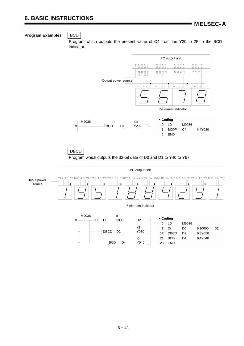
6. BASIC INSTRUCTIONS
6 − 41
MELSEC-A
Program Examples BCDProgram which outputs the present value of C4 from the Y20 to 2F to the BCDindicator.
DBCDProgram which outputs the 32-bit data of D0 and D1 to Y40 to Y67.
COM
Y2F
Y2E
Y2D
Y2C
Y2B
Y2A
Y29
Y28
Y27
Y26
Y25
Y24
Y23
Y22
Y21
Y20
8000
4000
2000
1000
800
400
200
100
80
40
20
10 8 4 2 1
0 1 0 1 0 1 1 0 0 1 1 1 1 0 0 0
PC output unit
Output power source
7-element indicator
•••• Coding0 LD M90361 BCDP C4 K4Y0206 END
0P K4
BCD C4 Y202M9036
Y67 to Y64Y63 to Y60Y5F to Y5CY5B to Y58Y57 to Y54Y53 to Y50Y4F to Y4CY4B to Y48Y47 to Y44Y43 to Y40
PC output unit
7-element indicator
Input powersource
•••• Coding0 LD M90361 D/ D0 K10000 D2
12 DBCD D2 K8Y05021 BCD D4 K4Y04026 END
0K
D/ D0 10000 D2M9036
K8DBCD D2 Y050
K4BCD D4 Y040

MEMO

6. BASIC INSTRUCTIONS
6 − 42
MELSEC-A
6.3.2 BCD 4-, 8-digit →→→→ BIN data conversion(BIN, BINP, DBIN, DBINP)
Available Device
Bit device Word (16-bit) device Constant Pointer Level Car
ryfla
g
Erro
rfla
g
X Y M L S B F T C D W R A0 A1 Z V K H P I N
Digi
t spe
cific
atio
n
Inde
x
M9012 (M9010, M9011)
(S) O O O O O O O O O O O O O O O OBIN
(D) O O O O O O O O O O O O O O O
K1toK4
(S) O O O O O O O O O O O O O ODBIN
(D) O O O O O O O O O O O O O
K1toK8
O O
Function BINConverts BCD data (0 to 9999) of device specified at (S) into BIN and transfers theresult to the device specified at (D).
ApplicableCPU All CPUs
(S) (D)
(S) (D)P
BIN conversion commands
(S)BCD data or headnumber of device whichstores BCD data
(D) Head number of devicewhich will store BIN data
Setting data
BIN, DBIN
Indicates the instruction symbol.
8000 4000 20001000 800 400 200 100 80 40 20 8 4 2 110
1 0 0 0 01 1 1 1 0 0 01 1 10
32768163848192 4096
0 0 1 0 0 1 1 1 0 0 0 0 1 1 1 1
2048 1024 512 256 128 64 32 16 8 4 2 1
Always set to 0.
(S) side BCD 9999
(D) side BIN 9999
BIN conversion
Unitsdigits
Tensdigits
Hundredsdigits
Thousandsdigits

6. BASIC INSTRUCTIONS
6 − 43
MELSEC-A
DBINConverts BCD data (0 to 99999999) of device specified at (S) into BIN and transfersthe result to the device specified at (D).
Execution Conditions
CAUTION
In some cases of execution of the BIN or DBIN instruction with a NO contact, operation erroroccurs due to BCD switch timing. It is recommended, when the BIN or DBIN instruction is used,that BIN data conversion be executed using the BIN conversion command after data setting.
Operation Error In the following case, operation error occurs and the error flag turns on.• Each digit of source (S) is outside the range of 0 to 9.
0 00 01 1 10 0 1 11 10 10 11 1 0 0 00 0 1 11 11 1 11
230
229
224
221
223
225
226
227
228
220
222
231
219
210
211
212
213
214
215
216
217
218
26
29
20
2122
23
24
25
27
28
4 2107
x
18 4 2106
18 4 2105
18 4 2104
18 4 2103
18 4 2102
18 4 2101
18 4 2100
18
x x x x x x x
1 00 00 1 01 1 1 10 01 10 01 0 1 1 00 1 1 00 11 0 10
Always set to 0.
(S) side BCD 99999999
(D) side BIN 99999999
BIN conversionTe
n m
illion
sdi
gits
(S)(S) + 1
Milli
ons
digi
ts
Hun
dred
thou
sand
sdi
gits
Ten
thou
sand
sdi
gits
Thou
sand
sdi
gits
Hun
dred
sdi
gits
Tens
dig
its
Uni
t dig
its
(D)(D) + 1
OFF
ON
Executedper scan
Executedper scan
Executedonly once
Executedonly once
P
BIN conversion command
K4BIN X020 D0
M9036 K4BIN X020 D0
X000
BIN conversioncommand
After data setting, X0 is turned ON and data isread.
Operation error sometimes occurs.
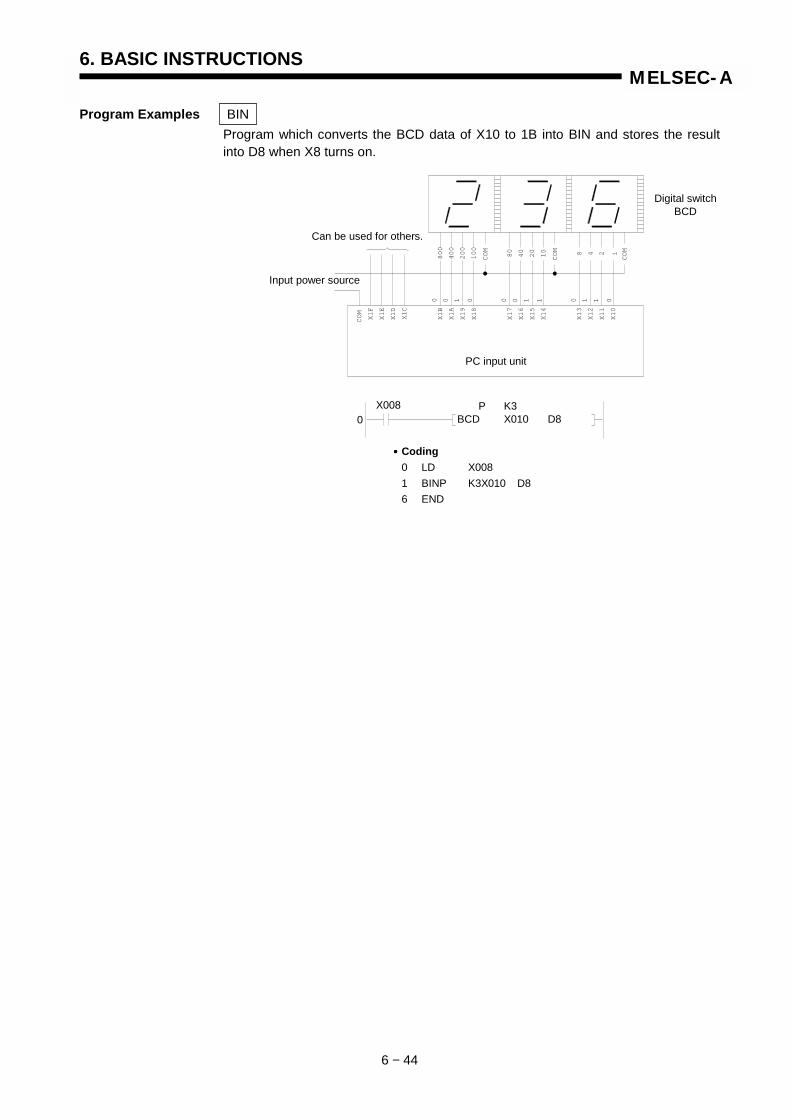
6. BASIC INSTRUCTIONS
6 − 44
MELSEC-A
Program Examples BINProgram which converts the BCD data of X10 to 1B into BIN and stores the resultinto D8 when X8 turns on.
800
400
200
100
80
40
20
10 8 4 2 1
COM
COM
COM
0 0 1 0 0 0 1 1 0 1 1 0
X1B
X1A
X19
X18
X1F
X1E
X1D
COM
X17
X16
X15
X14
X13
X12
X11
X10
X1C
PC input unit
Digital switchBCD
Can be used for others.
Input power source
•••• Coding0 LD X0081 BINP K3X010 D86 END
0P K3
BCD X010 D8X008
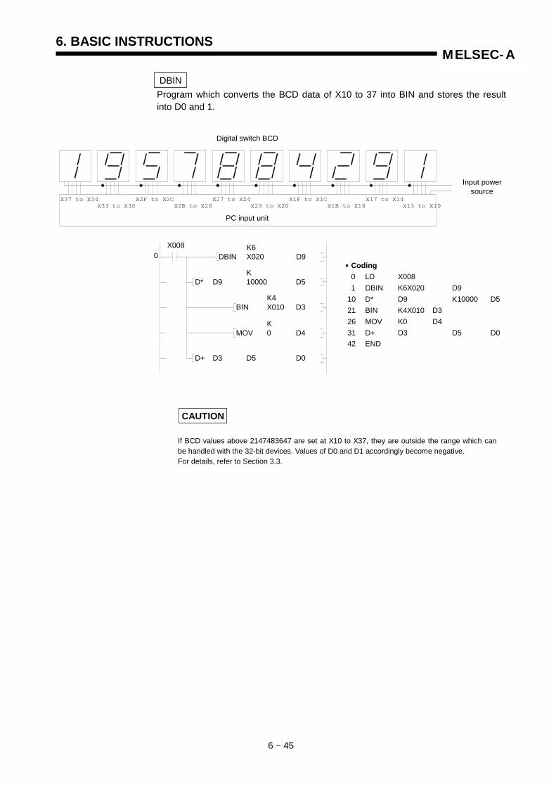
6. BASIC INSTRUCTIONS
6 − 45
MELSEC-A
DBINProgram which converts the BCD data of X10 to 37 into BIN and stores the resultinto D0 and 1.
CAUTION
If BCD values above 2147483647 are set at X10 to X37, they are outside the range which canbe handled with the 32-bit devices. Values of D0 and D1 accordingly become negative.For details, refer to Section 3.3.
X37 to X34X33 to X30
X2F to X2CX2B to X28
X27 to X24X23 to X20
X1F to X1CX1B to X18
X17 to X14X13 to X10
PC input unit
Digital switch BCD
Input powersource
•••• Coding0 LD X0081 DBIN K6X020 D9
10 D* D9 K10000 D521 BIN K4X010 D326 MOV K0 D431 D+ D3 D5 D042 END
0
KD* D9 10000 D5
X008 K6DBIN X020 D9
K4BIN X010 D3
KMOV 0 D4
D+ D3 D5 D0
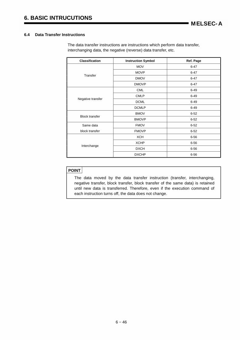
6. BASIC INTRUCUTIONS
6 − 46
MELSEC-A
6.4 Data Transfer Instructions
The data transfer instructions are instructions which perform data transfer,interchanging data, the negative (reverse) data transfer, etc.
Classification Instruction Symbol Ref. Page
MOV 6-47
MOVP 6-47
DMOV 6-47Transfer
DMOVP 6-47
CML 6-49
CMLP 6-49
DCML 6-49Negative transfer
DCMLP 6-49
BMOV 6-52Block transfer
BMOVP 6-52
FMOV 6-52Same data
block transfer FMOVP 6-52
XCH 6-56
XCHP 6-56
DXCH 6-56Interchange
DXCHP 6-56
POINT
The data moved by the data transfer instruction (transfer, interchanging,negative transfer, block transfer, block transfer of the same data) is retaineduntil new data is transferred. Therefore, even if the execution command ofeach instruction turns off, the data does not change.

MEMO

6. BASIC INTRUCUTIONS
6 − 47
MELSEC-A
6.4.1 16-, 32-bit data transfer(MOV, MOVP, DMOV, DMOVP)
Available Device
Bit device Word (16-bit) device Constant Pointer Level Car
ryfla
g
Erro
rfla
g
X Y M L S B F T C D W R A0 A1 Z V K H P I N
Digi
t spe
cific
atio
n
Inde
x
M9012 (M9010, M9011)
(S) O O O O O O O O O O O O O O O O O OMOV
(D) O O O O O O O O O O O O O O O
K1toK4
(S) O O O O O O O O O O O O O O O ODMOV
(D) O O O O O O O O O O O O O
K1toK8
O O
Functions MOVTransfers the 16-bit data of the device specified at (S) to the device specified at (D).
DMOVTransfers the 32-bit data of the device specified at (S) to the device specified at (D).
(S)
Transfer
1 0 0 1 11 0 0 0 1 1 10 0 11
(D) 1 0 0 1 11 0 0 0 1 1 10 0 11
16 bits
After transfer
Before transfer
(S)Data of transfer source orhead number of devicewhich stores data.
(D) Head number of device attransfer destination
MOV, DMOV
Indicates the instruction symbol.
Setting data
Transfer commands
(S) (D)
(S) (D)P
(S)
Transfer
(D)
32 bits
1 0 0 1 11 0 1 1 10 0 11
1 0 0 1 11 0 1 1 10 0 11
After transfer
Before transfer
ApplicableCPU All CPUs

6. BASIC INTRUCUTIONS
6 − 48
MELSEC-A
Execution Conditions
Programs Examples MOV(1) Program which stores the data of inputs X0 to B into D8.
(2) Program which stores 155 into D8 as a binary value when X8 turns on.
DMOV(1) Program which stores the data of A0 and A1 into D0 and D1.
(2) Program which stores the data of X0 to 1F into D0 and D1.
X90360 MOV x000 D8
P K3 • Coding0 LD M90361 MOVP K3X000 D86 END
• Coding0 LD M90361 DMOVP A0 D08 END
0 DMOV A0 D0PM9036
0 DMOV X000 D0X8
M9036• Coding
0 LD M90361 DMOVP K8X000 D08 END
OFF
ON
Executedper scan
Executedper scan
Executedonly once
Executedonly once
P
Transfer command
X0080 MOV 155 D8
P K • Coding0 LD X0081 MOVP K155 D86 END
009BH
b15
0000 11 00 00 00 11 10
b0
D8

6. BASIC INSTRUCTIONS
6 − 49
MELSEC-A
6.4.2 16-, 32-bit data negation transfer(CML, CMLP, DCML, DCMLP)
Available Device
Bit device Word (16-bit) device Constant Pointer Level Car
ryfla
g
Erro
rfla
g
X Y M L S B F T C D W R A0 A1 Z V K H P I N
Digi
t spe
cific
atio
n
Inde
x
M9012 (M9010, M9011)
(S) O O O O O O O O O O O O O O O O O OCML
(D) O O O O O O O O O O O O O O O
K1toK4
(S) O O O O O O O O O O O O O O O ODCML
(D) O O O O O O O O O O O O O
K1toK8
O O
Functions CMLReverses the 16-bit data of (S) per bit and transfers the result to (D).
DCMLReverses the 32-bit data of (S) per bit and transfers the result to (D).
ApplicableCPU All CPUs
(S)
Reverse
1 0 1 1 01 0 0 0 1 1 01 0 01
(D) 0 1 0 0 10 1 1 1 0 0 10 1 10
b0b15
Before execution
After execution
(S)
Reverse
(D)
b0b15
1 11 0 0 1 00 0 11 1 0 00 1
0 00 1 1 0 11 1 00 0 1 11 0
b0 b15
(S)(S)+1
(D)+1 (S)+1
Before execution
After execution
(S)Data to be reversed orhead number of devicewhich stores data
(D)Head number of devicewhich will store reverseresult
Setting data
CML, DCML
Indicates the instruction symbol.
(S) (D)
(S) (D)
Negative transfer commands
P

6. BASIC INSTRUCTIONS
6 − 50
MELSEC-A
Execution Conditions
Program Examples CML(1) Program which reverses the data of X0 to 7 and transfers the result to D0.
(2) Program which reverses the data of M16 to 31 and transfers the result to theY40 to 4F.
(3) Program which reverses the data of D0 and stores the result to D16 when X3turns on.
OFF
ON
Executedper scan
Executedper scan
Executedonly once
Executedonly once
P
Negative transfer command
0X003
CML D0 D16P
• Coding0 LD X0031 CML D0 D166 END
b15
0110 10 10 00 01 0
b0to
D16
CML
D0
b15 b0to
1001 01 01 11 10 11 11
00 0
0
• Coding0 LD M90381 CML K2X000 D06 END
M9038CML X000 D0
K2
b15
1111 00 01 11 11 11 11
to b8 b7 b0to
D0
CML
11 0 1 0 0 0 0
X7 to X0The number of bits of (S) < The number of bits of (D):
These bits areall regarded 0.
0M9038
CML M16 Y040K2 K3 • Coding
0 LD M90381 CML K2M16 K3Y0406 END
The number of bits of (S) < The number of bits of (D):
These bits areall regarded 0.
Y4B
1 0 001 11 11
toY48 Y47 Y40to
CML
1 10
00 1 0 011 1
M16toM23
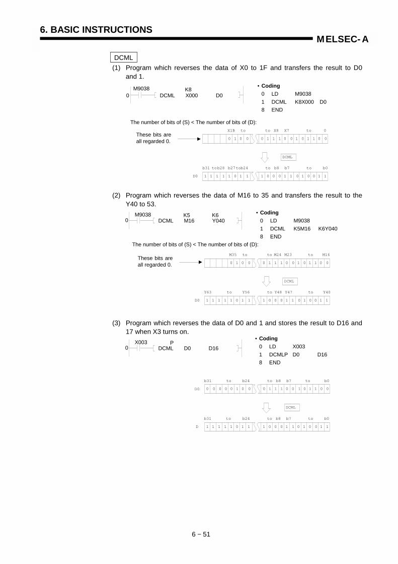
6. BASIC INSTRUCTIONS
6 − 51
MELSEC-A
DCML(1) Program which reverses the data of X0 to 1F and transfers the result to D0
and 1.
(2) Program which reverses the data of M16 to 35 and transfers the result to theY40 to 53.
(3) Program which reverses the data of D0 and 1 and stores the result to D16 and17 when X3 turns on.
0 0 11 10 1110 0 0 0 01 0
DCML
D0
X1B 0toX7X8toto
1 1 00 01 0001 1 1 1 10 1
b31 b0tob7b8toto
1 11 1
b28 b27 b24to
M90380 DCML X000 D0
K8• Coding
0 LD M90381 DCML K8X000 D08 END
The number of bits of (S) < The number of bits of (D):
These bits areall regarded 0.
0 0 11 10 1110 0 0 0 01 0
DCML
D0
M35 M16toM23M24toto
1 1 00 01 0001 1 1 1 10 1
Y63 Y40toY47Y48toto
1 11 1
Y56
M90380 DCML M16 Y040
K5 K6 • Coding0 LD M90381 DCML K5M16 K6Y0408 END
The number of bits of (S) < The number of bits of (D):
These bits areall regarded 0.
X0030 DCML D0 D16
P• Coding
0 LD X0031 DCMLP D0 D168 END
0 0 11 10 1110 0 0 0 01 0
D
b31 b0tob7b8toto
1 1 00 01 0001 1 1 1 10 1
b31 b0tob7b8to
1 11 1
b24to
0 0 0 0
b24
DCML
D0

MEMO

6. BASIC INSTRUCTIONS
6 − 52
MELSEC-A
6.4.3 16-bit data block transfer(BMOV, BMOVP, FMOV, FMOVP)
Available Device
Bit device Word (16-bit) device Constant Pointer Level Car
ryfla
g
Erro
rfla
g
X Y M L S B F T C D W R A0 A1 Z V K H P I N
Digi
t spe
cific
atio
n
Inde
x
M9012 (M9010, M9011)
(S) O O O O O O O O O O O O
(D) O O O O O O O O O O O
K1toK4BMOV
(n) O O
(S) O O O O O O O O O O O O O O O O O O
(D) O O O O O O O O O O O
K1toK4FMOV
(n) O O
O O
Functions BMOVTransfers the content of "n" points, which begin with the device specified at (S), inblocks to "n" points which begin with the device specified at (D).
• When the same devices have been specified at source and destination, datatransfer is possible. Transfer to the devices with the lower numbers is executedstarting with (S), and that to the devices with the higher numbers is executedstarting with (S) + (n-1).
• The number of (S) and (D) digits must be equal when both (S) and (D) are bitdevices.
(S)+(n-1) 8886
(S)+(n-2) 553F
(S)+3 6FFF
(S)+2 7FF0
(S)+1 5678
(S) 1234
Block transfer
(D)+(n-1) 8886
(D)+(n-2) 553F
(D)+3 6FFF
(D)+2 7FF0
(D)+1 5678
(D) 1234
n
ApplicableCPU All CPUs
Transfer commands
(S) (D) n
(S) (D) nP
(S)Head number of devicewhich stores data to betransferred
(D)Head number of devicewhich will store transfer-red data
n Number of transferredpoints
Setting data
BMOV, FMOV
Indicates the instruction symbol.
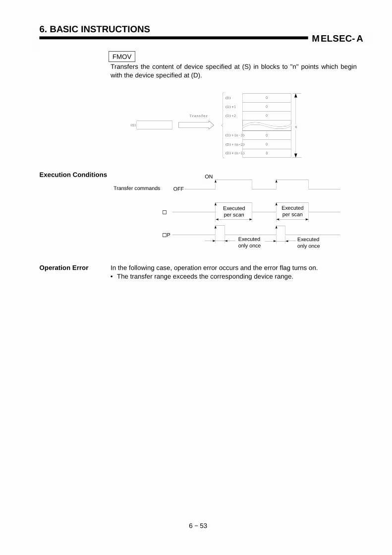
6. BASIC INSTRUCTIONS
6 − 53
MELSEC-A
FMOVTransfers the content of device specified at (S) in blocks to "n" points which beginwith the device specified at (D).
Execution Conditions
Operation Error In the following case, operation error occurs and the error flag turns on.• The transfer range exceeds the corresponding device range.
(S)
Transfer
(D)+(n-1)
0(D)+(n-2)
0
(D)+2 0
(D)+1 0
(D) 0
n
0
(D)+(n-3)
OFF
ON
Transfer commands
Executedper scan
Executedper scan
Executedonly once
Executedonly once
P
OFF
ON
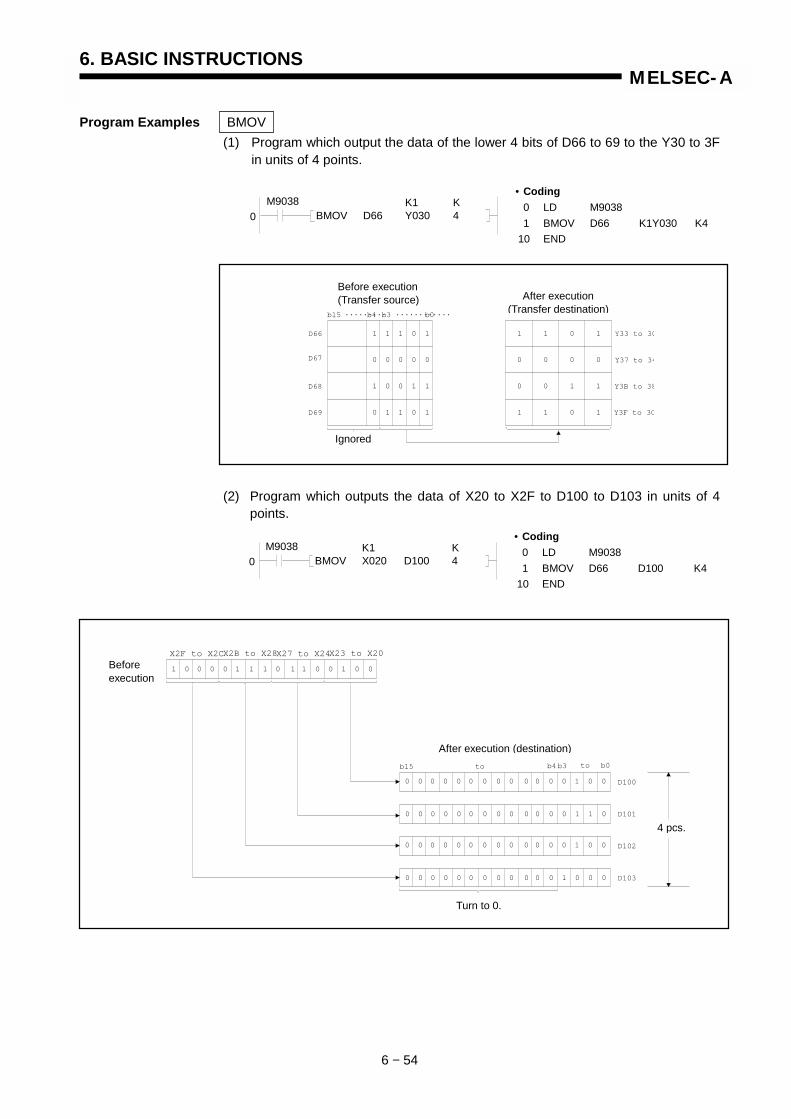
6. BASIC INSTRUCTIONS
6 − 54
MELSEC-A
Program Examples BMOV(1) Program which output the data of the lower 4 bits of D66 to 69 to the Y30 to 3F
in units of 4 points.
(2) Program which outputs the data of X20 to X2F to D100 to D103 in units of 4points.
M9038 K1 KBMOV D66 Y030 40
• Coding0 LD M90381 BMOV D66 K1Y030 K4
10 END
M9038 K1 KBMOV X020 D100 40
• Coding0 LD M90381 BMOV D66 D100 K4
10 END
11 1 10
00 0 00
01 0 11
10 1 10
b15 .........b4 b3 b0............
D67
D66
D68
D69
1 1 0 1
0 0 0 0
0 0 1 1
1 1 0 1
Y33 to 30
Y37 to 34
Y3B to 38
Y3F to 3C
Before execution(Transfer source) After execution
(Transfer destination)
Ignored
1 0 0 1 10 0 1 0 1 1 10 0 00
X2F to X2CX2B to X28X27 to X24X23 to X20
b15 to b4b3 to b0
0 0 0 0 00 0 0 0 0 0 10 0 00
0 0 0 0 00 0 0 0 0 0 10 0 01
0 0 0 0 00 0 0 0 0 0 10 0 00
0 0 0 0 00 0 0 0 0 0 00 1 00
D101
D100
D102
D103
Turn to 0.
Beforeexecution
After execution (destination)
4 pcs.
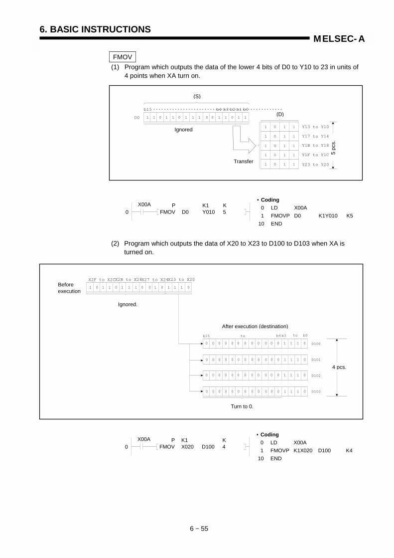
6. BASIC INSTRUCTIONS
6 − 55
MELSEC-A
FMOV(1) Program which outputs the data of the lower 4 bits of D0 to Y10 to 23 in units of
4 points when XA turn on.
(2) Program which outputs the data of X20 to X23 to D100 to D103 when XA is turned on.
• Coding0 LD X00A1 FMOVP D0 K1Y010 K5
10 END
0 P K1 KFMOV D0 Y010 5
X00A
• Coding0 LD X00A1 FMOVP K1X020 D100 K4
10 END
0 P K1 KFMOV X020 D100 4
X00A
1 0 1 1 11 0 1 0 0 1 10 1 01
X2F to X2CX2B to X28X27 to X24X23 to X20
b15 to b4b3 to b0
0 0 0 0 00 0 0 0 0 0 10 1 01
0 0 0 0 00 0 0 0 0 0 10 1 01
0 0 0 0 00 0 0 0 0 0 10 1 01
0 0 0 0 00 0 0 0 0 0 10 1 01
D101
D100
D102
D103
Beforeexecution
Ignored.
After execution (destination)
Turn to 0.
4 pcs.
1 1 0 0 11 1 1 1 0 0 01 1 11
b4b15 b3 b2 b1 b0
1 0 1 1
1 0 1 1
1 0 1 1
1 0 1 1
1 0 1 1
Y13 to Y10
Y17 to Y14
Y1B to Y18
Y1F to Y1C
Y23 to Y20
................................................
D0
(S)
(D)
5 pc
s.
Ignored
Transfer

6. BASIC INSTRUCTIONS
6 − 56
MELSEC-A
6.4.4 16-, 32-bit data exchange(XCH, XCHP, DXCH, DXCHP)
Available Device
Bit device Word (16-bit) device Constant Pointer Level Car
ryfla
g
Erro
rfla
g
X Y M L S B F T C D W R A0 A1 Z V K H P I N
Digi
t spe
cific
atio
n
Inde
x
M9012 (M9010, M9011)
(D1) O O O O O O O O O O O O O O OXCH
(D2) O O O O O O O O O O O O O O O
K1toK4
(D1) O O O O O O O O O O O O ODXCH
(D2) O O O O O O O O O O O O O
K1toK8
O O
Functions XCHInterchanges the 16-bit data of (D1) and (D2).
DXCHInterchanges the 32-bit data of (D1) and (D2).
ApplicableCPU All CPUs
1 0 0 1 010 11 00 0 10
16 bits 16 bits
(D1) (D2)
00 0 0 01 11 1 0 1 0 1 0
1 0 0 1 010 1 11 00 0 11 000 0 0 0 01 11 1 1 0 1 0 1 0
1 1 10Before execution
After execution
11 1 0 1 000 11 00 0 10 0 1 0 0 1 0 110 00 11 1 0 1 0
10 0 1 0 1100 11 1 0 1 0 1 1 0 1 0011 00 0 10 0 1
16 bits
(D1)
16 bits 16 bits 16 bits
(D1)+1 (D2)(D2)+2
0 0
Before execution
After execution
(D1)
(D2)
Head number of devicewhich stores data to beinterchanged
Setting data
XCH, DXCH
Indicates the instruction symbol.(D1) (D2)
(D1) (D2)
Interchange commands
P
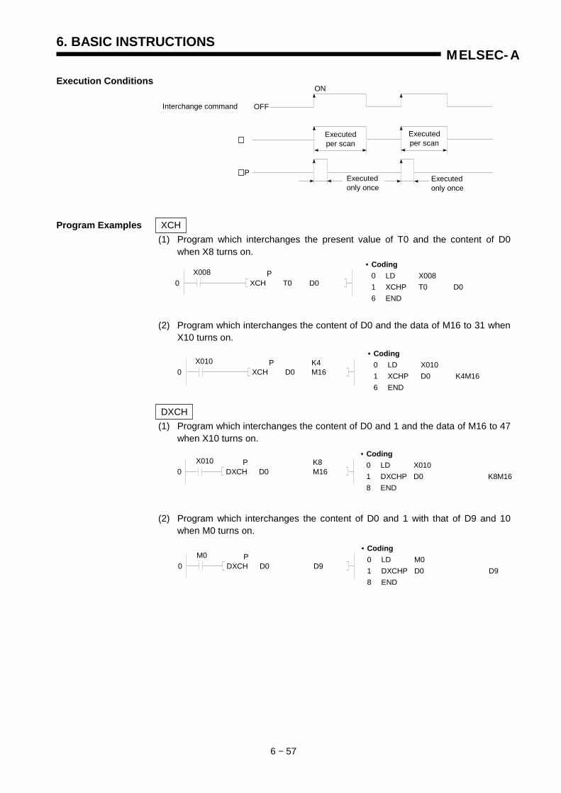
6. BASIC INSTRUCTIONS
6 − 57
MELSEC-A
Execution Conditions
Program Examples XCH(1) Program which interchanges the present value of T0 and the content of D0
when X8 turns on.
(2) Program which interchanges the content of D0 and the data of M16 to 31 whenX10 turns on.
DXCH(1) Program which interchanges the content of D0 and 1 and the data of M16 to 47
when X10 turns on.
(2) Program which interchanges the content of D0 and 1 with that of D9 and 10when M0 turns on.
0X008 P
XCH T0 D0
• Coding0 LD X0081 XCHP T0 D06 END
0X010 P K4
XCH D0 M16
• Coding0 LD X0101 XCHP D0 K4M166 END
• Coding0 LD X0101 DXCHP D0 K8M168 END
0X010 P K8
DXCH D0 M16
• Coding0 LD M01 DXCHP D0 D98 END
0M0 P
DXCH D0 D9
OFF
ON
Interchange command
Executedper scan
Executedper scan
Executedonly once
Executedonly once
P
OFF
ON
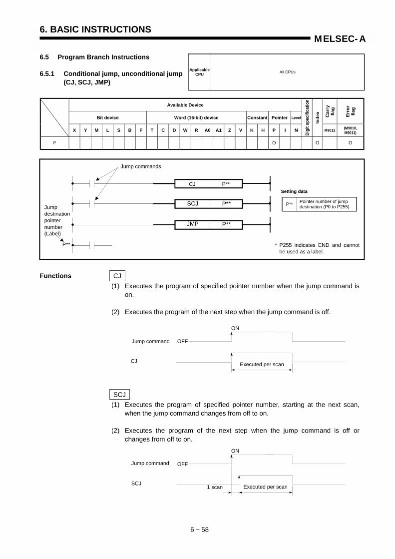
6. BASIC INSTRUCTIONS
6 − 58
MELSEC-A
6.5 Program Branch Instructions
6.5.1 Conditional jump, unconditional jump(CJ, SCJ, JMP)
Available Device
Bit device Word (16-bit) device Constant Pointer Level Car
ryfla
g
Erro
rfla
g
X Y M L S B F T C D W R A0 A1 Z V K H P I N
Digi
t spe
cific
atio
n
Inde
x
M9012 (M9010,M9011)
P O O O
Functions CJ(1) Executes the program of specified pointer number when the jump command is
on.
(2) Executes the program of the next step when the jump command is off.
SCJ(1) Executes the program of specified pointer number, starting at the next scan,
when the jump command changes from off to on.
(2) Executes the program of the next step when the jump command is off orchanges from off to on.
Jump commands
ApplicableCPU All CPUs
CJ P**
SCJ
JMP P**
P**Jumpdestinationpointernumber(Label)
P** * P255 indicates END and cannotbe used as a label.
Jump command
CJ Executed per scan
Jump command
SCJ1 scan Executed per scan
P** Pointer number of jumpdestination (P0 to P255)
Setting data
ON
OFF
ON
OFF

6. BASIC INSTRUCTIONS
6 − 59
MELSEC-A
JMP(1) Executes the program of specified pointer number unconditionally.
Consider the following when the jump instructions are used.
(2) Even if the timer, of which coil is on, is jumped by the CJ, SCJ, or JMPinstruction after the coil of timer is turned on, the timer continues counting.
(3) If the OUT instruction is jumped by CJ, SCJ or JMP, coil status is heldunchanged.
(4) When a jump is made to a memory location by CJ, SCJ, or JMP, the scan timeris shortened.
(5) The CJ, SCJ, and JMP instructions are also capable of jumping to a step withlower number. However, it is necessary to exit this closed loop before the watchdog timer times out.
(6) The device jumped by CJ, SCJ, or JMP does not change.
(7) The label (P**) occupies one step.
( )
( )
Closed loopwhen X3 isON.
P8 X000
X007
X003
X006P9
CJ P9
CJ P8
Y040
Y042
Exits the loop when X7 isturned ON.
( )
( )
( )
When XB turn on, jump is made to the label P19.
Even if XB and C turn on/off during the execution ofCJ instruction, Y43 and 49 do not change.
10
14
16
18
X00B
X00C
X00B
X009P19
CJ P19
Y043
Y049
Y04C
( )
( )
( )
( )
10
14
16
18
21
P9
X008
M33
M3
M36
X009
Occupiesone step.
CJ P9
Y030
Y036
Y039
Y03B
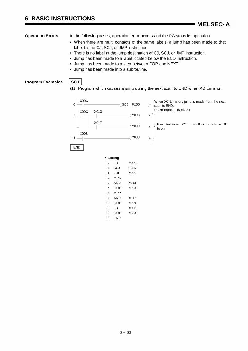
6. BASIC INSTRUCTIONS
6 − 60
MELSEC-A
Operation Errors In the following cases, operation error occurs and the PC stops its operation.• When there are mult. contacts of the same labels, a jump has been made to that
label by the CJ, SCJ, or JMP instruction.• There is no label at the jump destination of CJ, SCJ, or JMP instruction.• Jump has been made to a label located below the END instruction.• Jump has been made to a step between FOR and NEXT.• Jump has been made into a subroutine.
Program Examples SCJ(1) Program which causes a jump during the next scan to END when XC turns on.
( )
( )
( )
0
4
11
X00C
X00C
X00B
X013
X017
SCJ P255
Y093
Y099
Y083
When XC turns on, jump is made from the nextscan to END.(P255 represents END.)
Executed when XC turns off or turns from offto on.
END
• Coding0 LD X00C1 SCJ P2554 LDI X00C5 MPS6 AND X0137 OUT Y0938 MPP9 AND X017
10 OUT Y09911 LD X00B12 OUT Y08313 END

6. BASIC INSTRUCTIONS
6 − 61
MELSEC-A
(2) Program which causes a jump during the next scan to P3 when XC turns on.
CJ(3) Program which causes a jump to the END instruction when X9 turns on.
( )
( )
0
4
6P3
X00C
X030
X041
SCJ P3
Y06F
Y07E
• Coding0 LD X00C1 SCJ P34 LD X0305 OUT Y06F6 P37 LD X0418 OUT Y07E9 END
( )
( )
0
2X009
6
7
CJ P255
X000
X011
Y030
FEND
Y041
• Coding0 LD X0001 OUT Y0302 LD X0093 CJ P2556 FEND7 LD X0118 OUT Y0419 END

6. BASIC INSTRUCTIONS
6 − 62
MELSEC-A
6.5.2 Subroutine call, return(CALL, CALLP, RET)
Available Device
Bit device Word (16-bit) device Constant Pointer Level Car
ryfla
g
Erro
rfla
g
X Y M L S B F T C D W R A0 A1 Z V K H P I N
Digi
t spe
cific
atio
n
Inde
x
M9012 (M9010, M9011)
P O O O
Functions CALL, CALLP(1) Executes the subroutine program specified by the pointer (P**).
(2) Up to five levels of nesting of the CALL/CALLP instruction are allowed.
RET(1) Executes the sequence program located at the next step to the CALL(P)
instruction when the RET instruction is executed.
(2) Indicates the end of subroutine program.
POINT
For the PC CPUs shown below, setting indicated below is required.• A0J2HCPU, AnSCPU, AnSHCPU,A2CCPU, AnCPU, AnNCPU, A3HCPU,
A3MCPU, A3VCPUIn a sequence between the RET instruction in a subroutine program and theEND instruction at the end of a sequence program, a dummy circuit mustalways be set. Otherwise, the PC will fail to operate correctly.(A NOP instruction has the same effect. However, take it into considerationthat "NOP batch deletion" must not be executed by a peripheral device.)
ApplicableCPU All CPUs
Subroutine execution commands
P**
RET
CALL
P**Head pointer number ofsubroutine program (P0 to253)
Setting data
Subroutine program
P**CALLP
Call of subroutineprogram
Head pointer number(label) of subroutineprogram
Return ofsubroutineprogram
P**
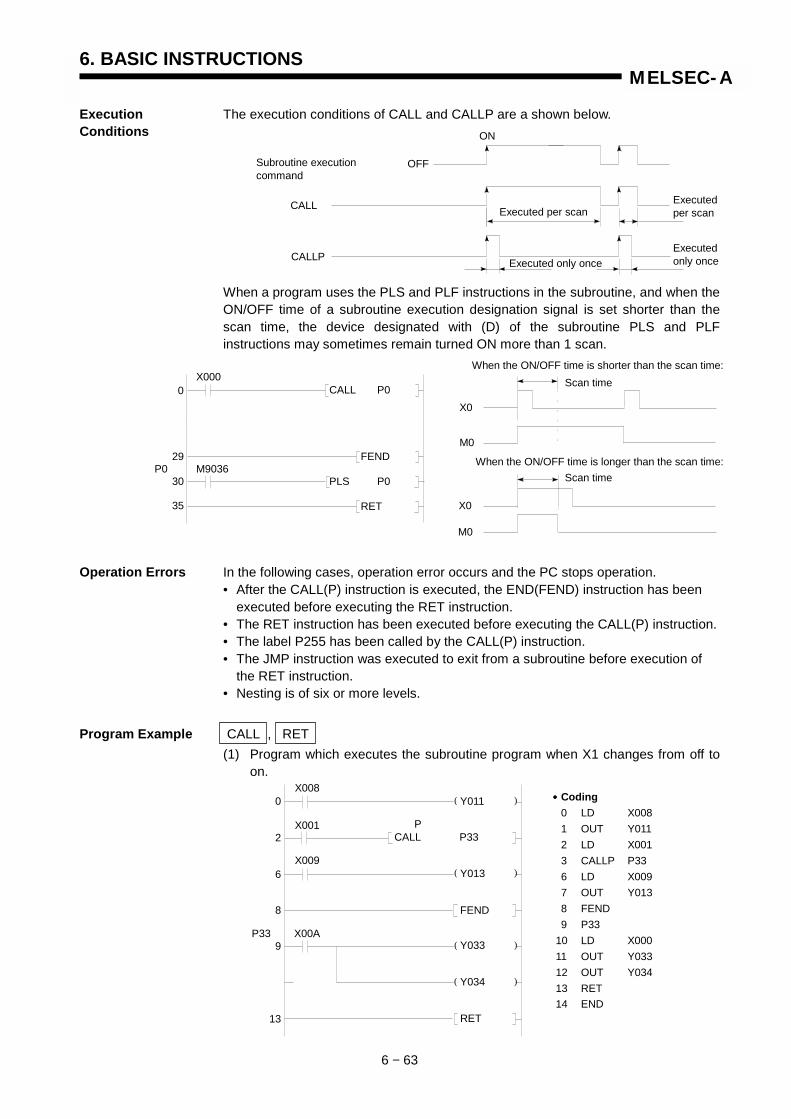
6. BASIC INSTRUCTIONS
6 − 63
MELSEC-A
Execution The execution conditions of CALL and CALLP are a shown below.Conditions
When a program uses the PLS and PLF instructions in the subroutine, and when theON/OFF time of a subroutine execution designation signal is set shorter than thescan time, the device designated with (D) of the subroutine PLS and PLFinstructions may sometimes remain turned ON more than 1 scan.
Operation Errors In the following cases, operation error occurs and the PC stops operation.• After the CALL(P) instruction is executed, the END(FEND) instruction has been
executed before executing the RET instruction.• The RET instruction has been executed before executing the CALL(P) instruction.• The label P255 has been called by the CALL(P) instruction.• The JMP instruction was executed to exit from a subroutine before execution of
the RET instruction.• Nesting is of six or more levels.
Program Example CALL , RET(1) Program which executes the subroutine program when X1 changes from off to
on.
OFF
ON
Executed per scanExecutedper scan
Executed only onceExecutedonly once
CALL
CALLP
Subroutine executioncommand
( )
( )
( )
( )
PCALL P33
Y011X008
0
2
6
P33
13
8
9
X001
X009
X00A
Y013
FEND
Y033
Y034
RET
•••• Coding0 LD X0081 OUT Y0112 LD X0013 CALLP P336 LD X0097 OUT Y0138 FEND9 P33
10 LD X00011 OUT Y03312 OUT Y03413 RET14 END
When the ON/OFF time is shorter than the scan time:
When the ON/OFF time is longer than the scan time:
X0
M0
X0
M0
Scan time
Scan time
CALL P0
FEND
X000
M9036PLS P0
RET
29
30
35
P0
0

6. BASIC INSTRUCTIONS
6 − 64
MELSEC-A
6.5.3 Interrupt enable, disable, return(EI, DI, IRET)
The EI and DI instructions used with the AnN, AnS, AnSH, A1FX, A0J2H and A73vary in function with status of special relay M9053, as mentioned below.When M9053 is ON: Link refresh enable/disable
(See Section 6.7.2 for details.)When M9053 is OFF: Interrupt enable/disable
Available Device
Bit device Word (16-bit) device Constant Pointer Level Car
ryfla
g
Erro
rfla
g
X Y M L S B F T C D W R A0 A1 Z V K H P I N
Digi
t spe
cific
atio
n
Inde
x
M9012 (M9010, M9011)
Functions DI(1) Disables the interrupt program until the EI instruction is executed so that
interrupt signals are ignored.
(2) When the PC CPU is RESET, interrupt program execution is disabled.
EI(1) Enables the interrupt program.
AnSAnN
AnSHAn A1FX A3H
A3M A3V AnA
AnU, A2ASA2USH-S1
A2USH boardQCPU-A(A Mode)
A0J2H A2CA52G A73 A3N
boardApplicableCPU
O O X O O X
Remark * EI and DI instructions are valid only when special relay M9053 is OFF.
EI Programexecution continues
IRET Interruptprogram
Required to the AnN, AnS,AnSH, A1FX, A0J2H, A73and A3N board
Interrupt pointer (10 to 31)(Label)
M9036RST M9053
RST M9053
DI
EI
IRET
M9036
I**
Sequence program
Sequence program
Interrupt program
DI
EI
FENDIn
Any interrupt signal occuring betweenDI and EI instructions, is disableduntil the processing between the DIand EI instructions is completed afterwhich the interrupt program is run.
* * * * *
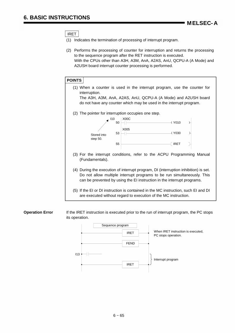
6. BASIC INSTRUCTIONS
6 − 65
MELSEC-A
IRET(1) Indicates the termination of processing of interrupt program.
(2) Performs the processing of counter for interruption and returns the processingto the sequence program after the RET instruction is executed.With the CPUs other than A3H, A3M, AnA, A2AS, AnU, QCPU-A (A Mode) andA2USH board interrupt counter processing is performed.
POINTS
(1) When a counter is used in the interrupt program, use the counter forinterruption.The A3H, A3M, AnA, A2AS, AnU, QCPU-A (A Mode) and A2USH boarddo not have any counter which may be used in the interrupt program.
(2) The pointer for interruption occupies one step.
(3) For the interrupt conditions, refer to the ACPU Programming Manual(Fundamentals).
(4) During the execution of interrupt program, DI (interruption inhibition) is set.Do not allow multiple interrupt programs to be run simultaneously. Thiscan be prevented by using the EI instruction in the interrupt programs.
(5) If the EI or DI instruction is contained in the MC instruction, such EI and DIare executed without regard to execution of the MC instruction.
Operation Error If the IRET instruction is executed prior to the run of interrupt program, the PC stops its operation.
( )
( )I10
50X00C
X005
Y010
Y030
IRET
53
55
Stored intostep 50.
Sequence program
IRET
FEND
IRET
I13
When IRET instruction is executed,PC stops operation.
Interrupt program
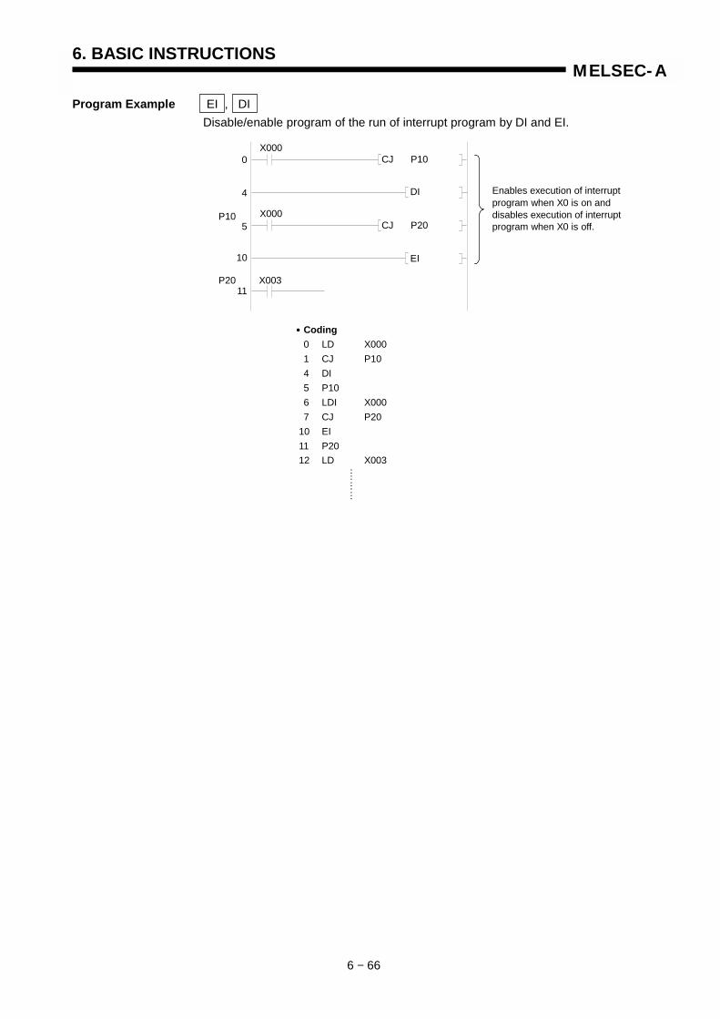
6. BASIC INSTRUCTIONS
6 − 66
MELSEC-A
Program Example EI , DIDisable/enable program of the run of interrupt program by DI and EI.
CJ P20
X0000
4
5
10
X000
X003
DI
EI
11
CJ P10
Enables execution of interruptprogram when X0 is on anddisables execution of interruptprogram when X0 is off.
P20
P10
•••• Coding0 LD X0001 CJ P104 DI5 P106 LDI X0007 CJ P20
10 EI11 P2012 LD X003
……
….

MEMO

6. BASIC INSTRUCTIONS
6 − 67
MELSEC-A
6.5.4 Microcomputer program call(SUB, SUBP)
The SUB instruction of the AnA, A2AS, AnU, QCPU-A (A Mode) and A2USH boardbecomes the 16-bit constant setting instruction in the extension applicationinstructions. For details, refer to the AnSHCPU/AnACPU/AnUCPU ProgrammingManual (Dedicated Instructions).
Available Device
Bit device Word (16-bit) device Constant Pointer Level Car
ryfla
g
Erro
rfla
g
X Y M L S B F T C D W R A0 A1 Z V K H P I N
Digi
t spe
cific
atio
n
Inde
x
M9012 (M9010, M9011)
n O O O O O O O O O O O O O
Functions (1) Calls the microcomputer program created by user and allows the run ofmicrocomputer program.
(2) When the run of microcomputer program is completed, runs the sequenceprogram again, starting at the next step to the SUB or SUBP instruction.
(3) The SUB and SUBP instructions can be used for the sequence program andsubsequence program.
AnSAnN
AnSHAn A1FX A3H
A3M A3V AnA
AnU, A2ASA2USH-S1
A2USH boardQCPU-A(A Mode)
A0J2H A2CA52G A73 A3N
boardApplicableCPU
O O O O O X X O O O O
Remark
n Head address of micro-computer program
Setting data
Microcomputer program execution commands
nSUB
nSUBP
ParameterSet value of
timer/counter
SUB(P)
ENDMicrocomputer
programRET
Sequence programarea
Microcomputerprogram area
Main (sub)program area
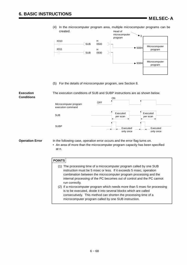
6. BASIC INSTRUCTIONS
6 − 68
MELSEC-A
(4) In the microcomputer program area, multiple microcomputer programs can becreated.
(5) For the details of microcomputer program, see Section 8.
Execution The execution conditions of SUB and SUBP instructions are as shown below.Conditions
Operation Error In the following case, operation error occurs and the error flag turns on.• An area of more than the microcomputer program capacity has been specified
at n.
POINTS
(1) The processing time of a microcomputer program called by one SUBinstruction must be 5 msec or less. If it exceeds 5 msec, operationcombination between the microcomputer program processing and theinternal processing of the PC becomes out of control and the PC cannotrun correctly.
(2) If a microcomputer program which needs more than 5 msec for processingis to be executed, divide it into several blocks which are calledconsecutively. This method can shorten the processing time of amicrocomputer program called by one SUB instruction.
HSUB 0930
X010
X011
HSUB 0500
500H Microcomputerprogram
930H Microcomputerprogram
0
Head ofmicrocomputerprogram
OFF
ON
Executedper scan
Executedper scan
Executedonly once
Executedonly once
SUB
SUBP
Microcomputer programexecution command
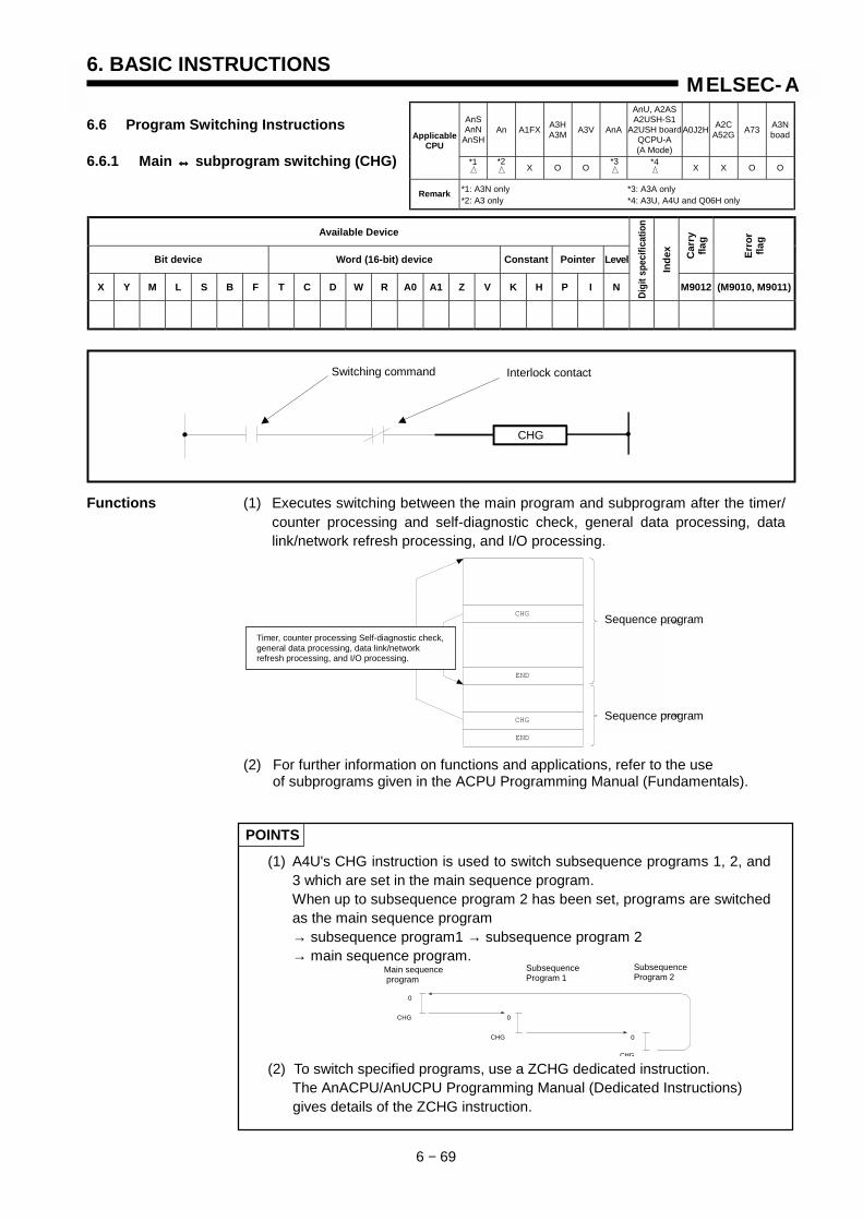
6. BASIC INSTRUCTIONS
6 − 69
MELSEC-A
6.6 Program Switching Instructions
6.6.1 Main ↔↔↔↔ subprogram switching (CHG)
Available Device
Bit device Word (16-bit) device Constant Pointer Level Car
ryfla
g
Erro
rfla
g
X Y M L S B F T C D W R A0 A1 Z V K H P I N
Digi
t spe
cific
atio
n
Inde
x
M9012 (M9010, M9011)
Functions (1) Executes switching between the main program and subprogram after the timer/counter processing and self-diagnostic check, general data processing, datalink/network refresh processing, and I/O processing.
(2) For further information on functions and applications, refer to the useof subprograms given in the ACPU Programming Manual (Fundamentals).
POINTS
(1) A4U's CHG instruction is used to switch subsequence programs 1, 2, and3 which are set in the main sequence program.When up to subsequence program 2 has been set, programs are switchedas the main sequence program→ subsequence program1 → subsequence program 2→ main sequence program.
(2) To switch specified programs, use a ZCHG dedicated instruction.The AnACPU/AnUCPU Programming Manual (Dedicated Instructions)
AnSAnN
AnSHAn A1FX A3H
A3M A3V AnA
AnU, A2ASA2USH-S1
A2USH boardQCPU-A(A Mode)
A0J2H A2CA52G A73 A3N
boadApplicableCPU
X O O X X O O
Remark *1: A3N only *3: A3A only*2: A3 only *4: A3U, A4U and Q06H only
Switching command Interlock contact
CHG
*1 *2 *3 *4
Main sequence program
SubsequenceProgram 1
SubsequenceProgram 2
CHG
CHG
CHG
0
0
0
CHG
END
CHG
Sequence program
END
Sequence program
Timer, counter processing Self-diagnostic check,general data processing, data link/networkrefresh processing, and I/O processing.
Sequence program
Sequence program
gives details of the ZCHG instruction.

6. BASIC INSTRUCTIONS
6 − 70
MELSEC-A
Execution (1) When the A3 is used, the CHG instruction is only executed on the leading edgeConditions of its input condition. Since operation result of the input condition changes with
status of M9050, execution contents of the CHG instruction change with status of M9050.
Status of M9050
OFF ON
Ladder example
The following program is written before END or FEND of the main and subsequence programs.
Timing chart
OFF No switching between the main and subsequenceprograms. (4), 5), 11))
No switching between the main and subsequenceprograms (4), 5), 11))
ONCHG instruction is executed every scan and switchesbetween the main and subsequence programs.(2), 3), 7), 8), 9), 10))
The main sequence program is only switched to thesubsequence program, then back to the main sequ-ence program on the first leading edge of the CHGinstruction execution command (X0). (2))
Operationdepending on
ON/OFF ofX0
OFF↓
ON
Switched between the main and subsequence prog-rams ( 1), 6), 12))
Switched between the main and subsequence prog-rams ( 1), 6), 12))
Remarks When the CHG instruction is executed, END processing (e.g. timer timing, counter counting, WDT reset) isperformed for the current program and operation is started from step 0 of the other program.
(2) When the A3N, A73, A3V and A3N board are used, the CHG instruction is onlyexecuted on the leading edge of its input condition. Since M9050 is notprovided, execution contents of the CHG instruction are always same.
Ladder example
The following program is written before END or FEND of the main and subsequence programs.
Timing chart
OFF No switching between the main and subsequence programs. (4), 5), 11))
ON The main sequence program is only switched to the subsequence program, then back to the main sequenceprogram on the first leading edge of the CHG instruction execution command (X0). (2))
Operationdependingon ON/OFF
of X0OFF
↓ON
Switched between the main and subsequence programs ( 1), 6), 12))
Remarks When the CHG instruction is executed, END processing (e.g. timer timing, counter counting, WDT reset) isperformed for the current program and operation is started from step 0 of the other program.
X0CHG instructionexecution in mainsequence programMain sequenceprogram
Subsequence program
CHG instructionexecution insubsequence program
OFF
ON
1) 2) 3) 4) 5) 6) 7) 8) 9) 10) 11) 12)
X0CHG instructionexecution in mainsequence programMain sequenceprogram
Subsequence program
CHG instructionexecution insubsequence program
OFF
ON
1) 2) 3) 4) 5) 6) 7) 8) 9) 10) 11) 12)
X000 Inter lockCHG
Input condition
X000 InterlockCHG
Input condition
X0CHG instructionexecution in mainsequence programMain sequenceprogram
Subsequence program
CHG instructionexecution insubsequence program
OFF
ON
1) 2) 3) 4) 5) 6) 7) 8) 9) 10) 11) 12)

6. BASIC INSTRUCTIONS
6 − 71
MELSEC-A
(3) When the A3H, A3M, AnA, A3U, A4U and Q06H are used, the CHG instructionis executed repeatedly while its input condition is on.
Ladder exampleThe following program is written before END or FEND of the main and subsequence programs.
Timing chart
OFF No switching between the main and subsequence programs. (4), 5), 11))
ON CHG instruction is executed every scan and switches between the main and subsequence programs. (2), 3),7), 8), 9), 10))
Operationdependingon ON/OFF
of X0 OFF
ONSwitched between the main and subsequence programs (1), 6), 12))
Remarks When the CHG instruction is executed, END processing (e.g. timer timing, counter counting, WDT reset) isperformed for the current program and operation is started from step 0 of the other program.
X0
CHG instruction executionin main sequence program
Main sequence program
Subsequence program
CHG instruction executionin subsequence program
OFF
ON
1) 2) 3) 4) 5) 6) 7) 8) 9) 10) 11) 12)
X000 Inter lockCHG
↓
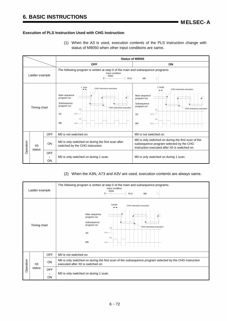
6. BASIC INSTRUCTIONS
6 − 72
MELSEC-A
Execution of PLS Instruction Used with CHG Instruction
(1) When the A3 is used, execution contents of the PLS instruction change withstatus of M9050 when other input conditions are same.
Status of M9050
OFF ON
Ladder example
The following program is written at step 0 of the main and subsequence programs.
Timing chart
OFF M0 is not switched on. M0 is not switched on.
ON M0 is only switched on during the first scan afterswitched by the CHG instruction.
M0 is only switched on during the first scan of thesubsequence program selected by the CHGinstruction executed after X0 is switched on.
Ope
ratio
n
X0status
OFF↓
ONM0 is only switched on during 1 scan. M0 is only switched on during 1 scan.
(2) When the A3N, A73 and A3V are used, execution contents are always same.
Ladder example
The following program is written at step 0 of the main and subsequence programs.
Timing chart
OFF M0 is not switched on.
ON M0 is only switched on during the first scan of the subsequence program selected by the CHG instructionexecuted after X0 is switched on.
Ope
ratio
n
X0status OFF
↓ON
M0 is only switched on during 1 scan.
X000PLS M0
Input condition
Main sequenceprogram run
Subsequenceprogram run
X0
M0
OFF
ON
OFF
ON
CHG instruction execution
CHG instruction execution1 scan
Main sequenceprogram run
Subsequenceprogram run
X0
M0
OFF
ON
OFF
ON
CHG instruction execution
CHG instruction execution
1scan
CHG instruction execution
OFF
ON
OFF
ON
Main sequenceprogram run
Subsequenceprogram run
X0
M0
1 scan
CHG instruction execution
X000PLS M0
Input condition
0
0
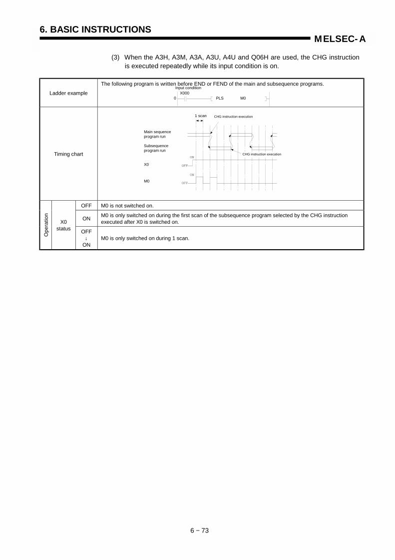
6. BASIC INSTRUCTIONS
6 − 73
MELSEC-A
(3) When the A3H, A3M, A3A, A3U, A4U and Q06H are used, the CHG instructionis executed repeatedly while its input condition is on.
Ladder example
The following program is written before END or FEND of the main and subsequence programs.
Timing chart
OFF M0 is not switched on.
ON M0 is only switched on during the first scan of the subsequence program selected by the CHG instructionexecuted after X0 is switched on.
Ope
ratio
n
X0status OFF
↓ON
M0 is only switched on during 1 scan.
X000PLS M0
Input condition
Main sequenceprogram run
Subsequenceprogram run
X0
M0
OFF
ON
OFF
ON
CHG instruction execution
CHG instruction execution
1 scan
0

6. BASIC INSTRUCTIONS
6 − 74
MELSEC-A
Execution of P Instruction Used with CHG Instruction
(1) When the A3 is used, execution contents of the PLS instruction change withstatus of M9050 when other input conditions are same.
Status of M9050
OFF ON
Ladder example
The following program is written at step 0 of the main and subsequence programs.
Timing chart
OFF MOVP instruction is not executed. MOVP instruction is not executed.
ON The MOVP instruction is executed during the firstscan after switched by the CHG instruction.
MOVP instruction is only executed during the firstscan of the subsequence program selected by theCHG instruction executed after X0 is switched on.
Operationdepending
on X0ON/OFFstatus
OFF↓
ONMOVP instruction is only executed once. MOVP instruction is only executed once.
(2) When the A3N, A73 and A3V are used, execution contents are always same.
Ladder example
The following program is written at step 0 of the main and subsequence programs.
Timing chart
OFF MOVP instruction is not executed.
ON MOVP instruction is only executed duing the first scan of the subsequence program selected by the CHGinstruction executed after X0 is switched on.
Operationdepending
on X0ON/OFFstatus
OFF↓
ONMOVP instruction is only executed once.
CHG instruction execution1 scan
OFF
ON
OFF
ON
Main sequenceprogram run
Subsequenceprogram run
X0
MOVP
CHG instruction execution
OFF
ON
OFF
ON
CHG instruction execution1 scan
Main sequenceprogram run
Subsequenceprogram run
X0
MOVP
CHG instruction execution
CHG instruction execution1scan
Main sequenceprogram run
Subsequenceprogram run
X0
MOVP
OFF
ON
OFF
ON
CHG instruction execution
MOVPX000
X000MOV 0 D0
P K
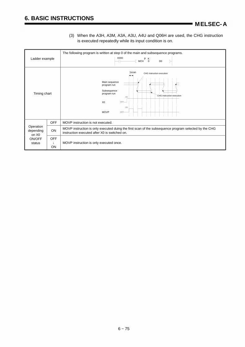
6. BASIC INSTRUCTIONS
6 − 75
MELSEC-A
(3) When the A3H, A3M, A3A, A3U, A4U and Q06H are used, the CHG instructionis executed repeatedly while its input condition is on.
Ladder example
The following program is written at step 0 of the main and subsequence programs.
Timing chart
OFF MOVP instruction is not executed.
ON MOVP instruction is only executed duing the first scan of the subsequence program selected by the CHGinstruction executed after X0 is switched on.
Operationdepending
on X0ON/OFFstatus
OFF↓
ONMOVP instruction is only executed once.
CHG instruction execution1scan
Main sequenceprogram run
Subsequenceprogram run
X0
MOVP
OFF
ON
OFF
ON
CHG instruction execution
X000MOV 0 D0
P K
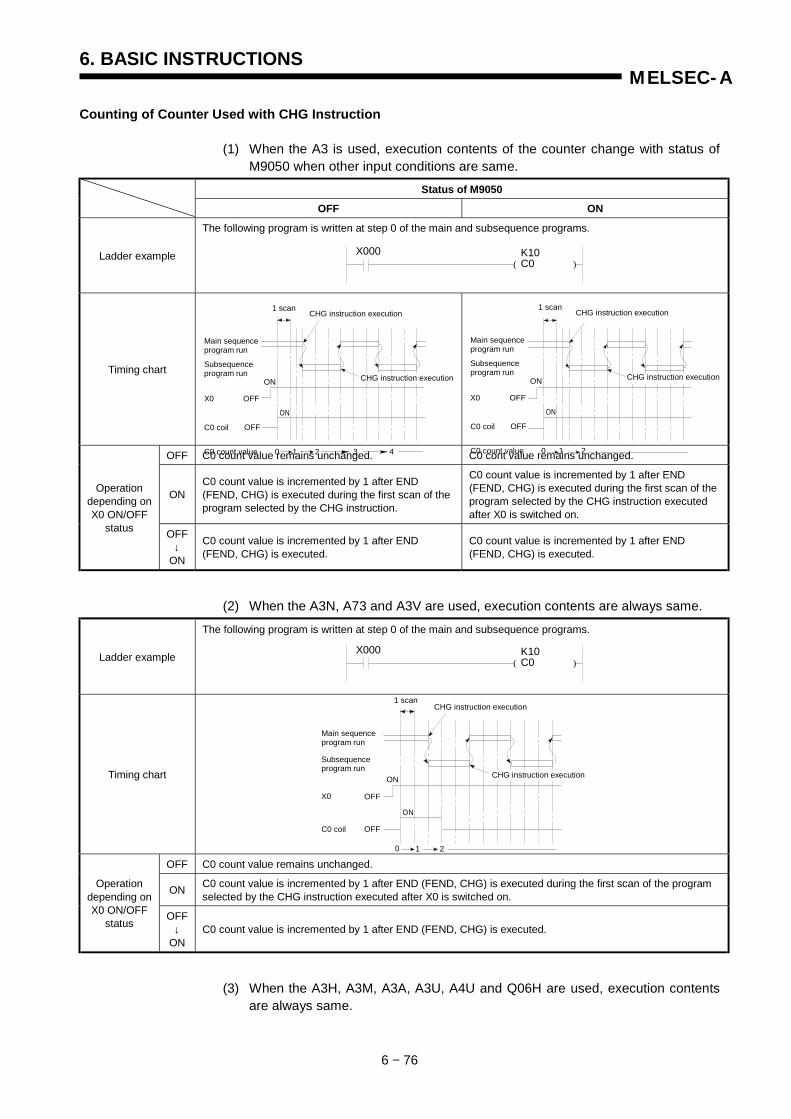
6. BASIC INSTRUCTIONS
6 − 76
MELSEC-A
Counting of Counter Used with CHG Instruction
(1) When the A3 is used, execution contents of the counter change with status ofM9050 when other input conditions are same.
Status of M9050
OFF ON
Ladder example
The following program is written at step 0 of the main and subsequence programs.
Timing chart
OFF C0 count value remains unchanged. C0 cont value remains unchanged.
ONC0 count value is incremented by 1 after END(FEND, CHG) is executed during the first scan of theprogram selected by the CHG instruction.
C0 count value is incremented by 1 after END(FEND, CHG) is executed during the first scan of theprogram selected by the CHG instruction executedafter X0 is switched on.
Operationdepending onX0 ON/OFF
status OFF↓
ON
C0 count value is incremented by 1 after END(FEND, CHG) is executed.
C0 count value is incremented by 1 after END(FEND, CHG) is executed.
(2) When the A3N, A73 and A3V are used, execution contents are always same.
Ladder example
The following program is written at step 0 of the main and subsequence programs.
Timing chart
OFF C0 count value remains unchanged.
ON C0 count value is incremented by 1 after END (FEND, CHG) is executed during the first scan of the programselected by the CHG instruction executed after X0 is switched on.
Operationdepending onX0 ON/OFF
statusOFF
↓ON
C0 count value is incremented by 1 after END (FEND, CHG) is executed.
(3) When the A3H, A3M, A3A, A3U, A4U and Q06H are used, execution contentsare always same.
( )X000 K10
C0
1 scan
Main sequenceprogram run
CHG instruction execution
Subsequenceprogram run
X0 OFF
ON
C0 coil OFF
ON
C0 count value 1 20 3 4
CHG instruction execution
1 scan
Main sequenceprogram run
CHG instruction execution
Subsequenceprogram run
X0 OFF
ON
C0 coil OFF
ON
C0 count value 1 20
CHG instruction execution
( )X000 K10
C0
1 scanCHG instruction execution
Main sequenceprogram run
Subsequenceprogram run
CHG instruction execution
X0 OFF
ON
C0 coil OFF
0 1
ON
2
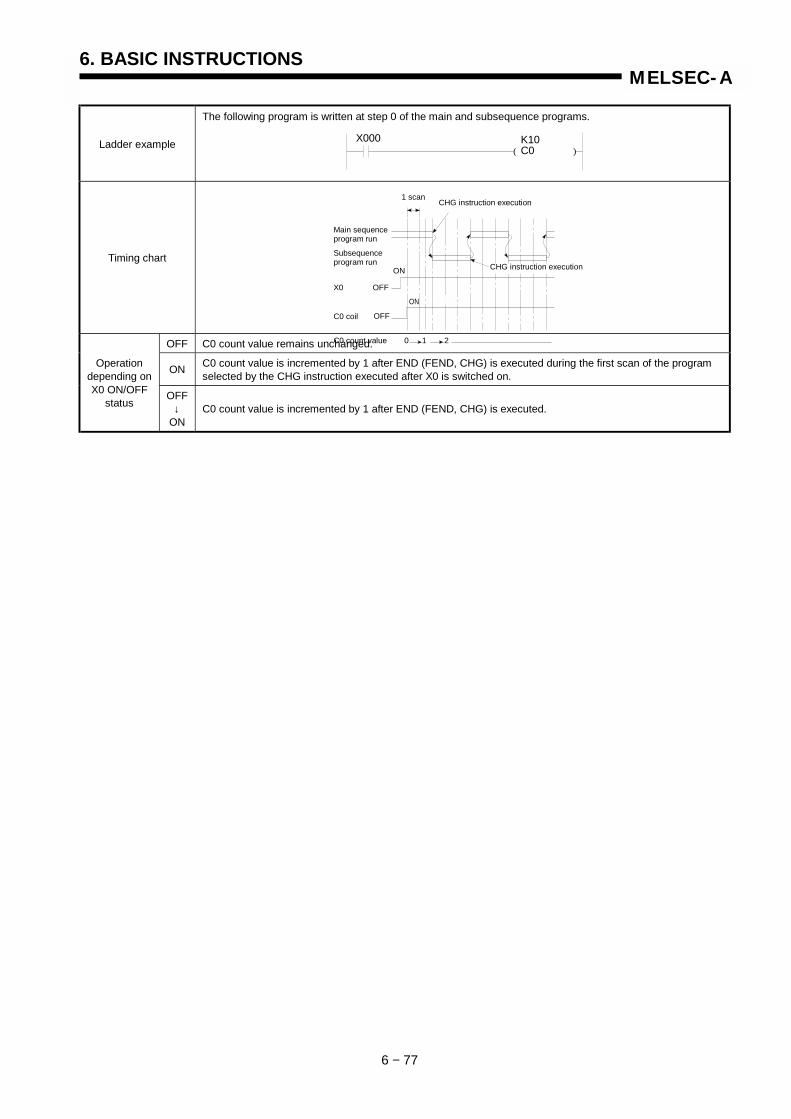
6. BASIC INSTRUCTIONS
6 − 77
MELSEC-A
Ladder example
The following program is written at step 0 of the main and subsequence programs.
Timing chart
OFF C0 count value remains unchanged.
ON C0 count value is incremented by 1 after END (FEND, CHG) is executed during the first scan of the programselected by the CHG instruction executed after X0 is switched on.
Operationdepending onX0 ON/OFF
statusOFF
↓ON
C0 count value is incremented by 1 after END (FEND, CHG) is executed.
( )X000 K10
C0
1 scan
Main sequenceprogram run
CHG instruction execution
Subsequenceprogram run
X0 OFF
ON
C0 coil OFF
ON
C0 count value 1 20
CHG instruction execution

6. BASIC INSTRUCTIONS
6 − 78
MELSEC-A
Timing of Timer Used with CHG Instruction
Each of the CPUs with which the CHG instruction can be used has two timer setvalue storage areas; one for the main sequence program and the other for thesubsequence program.In these areas, the set value of the timer not in use is 0. The set value of 0 isregarded as infinite and the timer does not time out.When the main (sub) sequence program is switched to the sub (main) sequenceprogram by the CHG instruction after the timer in the main (sub) sequence programhas started timing, the timer does not time out during execution of the sub (main)program because the timer set value specified in the main (sub) program is 0 in thesub (main) program timer set value storage area.
Ladder example
The following program is written after the main sequence program and the same timer number is not used inthe subsequence program.
Timing chart
OperationT200 started by the main sequence program does not time out while the subsequence program is running.It times out on the following condition when the main sequence program is run again:
(Present value) < 0 or (set value) < (present value)
( )X000 K15
T200
Main sequenceprogram runSubsequenceprogram run
X0
T200 coil
The timer does not time outas the set value in the sub-sequence program is 0.
The timer times out as theset value is greater than thepresent value. In this case,the value monitored is 15.
T200 contact
END1 scan
40 ms
END END END
20 ms
CHG
60 ms
END END END END END ENDCHG
40 ms
OUT T 200
ON
OFF
ON
ON
OFF
OFF
4 4 4 42 6 6 6 6 6 6
0+4=4
0 4+4=8
8+4=12
12+2=14
14+6=20
20+6=26
26+6=32
32+6=38
38+6=44
44+4=48
48+6=54
T200 coil is not switched off asOUT T200 is not executed whenX0 is switched off.
10ms timer tim-ing value
T200 presentvalue
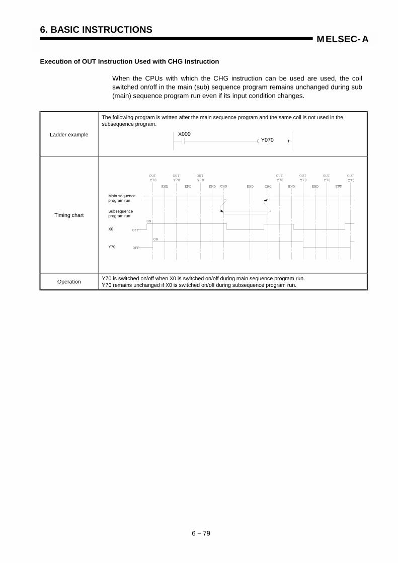
6. BASIC INSTRUCTIONS
6 − 79
MELSEC-A
Execution of OUT Instruction Used with CHG Instruction
When the CPUs with which the CHG instruction can be used are used, the coilswitched on/off in the main (sub) sequence program remains unchanged during sub(main) sequence program run even if its input condition changes.
Ladder example
The following program is written after the main sequence program and the same coil is not used in thesubsequence program.
Timing chart
Operation Y70 is switched on/off when X0 is switched on/off during main sequence program run.Y70 remains unchanged if X0 is switched on/off during subsequence program run.
( )X000
END END END END END END END
OUTY70
OUTY70
OUTY70
OUTY70
OUTY70
OUTY70
OUTY70
CHG CHG
ON
ON
OFF
OFF
Main sequenceprogram run
Subsequenceprogram run
X0
Y70
Y070

6. BASIC INSTRUCTIONS
6 − 80
MELSEC-A
Program Examples CHG
The following programs are used with the A3CPU and other types of CPUs to outputpulses in accordance with the input condition of the PLS instruction while alternately running the main and subprograms.
(1) For A3CPUIt is necessary to compare the operation result of a scan with that of theprevious scan to allow correct output of the PLS instruction. M9050 musttherefore be turned ON when the CHG instruction is executed to save theoperation result of the previous scan, which has been stored in the operationresult storage memory, in the save area.Since the CHG instruction for the A3CPU is executed only when inputconditions are turned ON, programs must be written in the forms shown below.
(2) For A3N, A73 and A3V CPUsSince the CHG instruction for the A3NCPU is executed only when inputconditions are turned ON, programs must be written in the forms shown below.
( )
( )
Main sequence program Sub sequence program
( )( )
( )
( )
M9036
M0
M0
M0
M0
M0
P0
P1
M9051
M9051
M9051
M9057
M9057
M9050
M0
CJ P1
CHG
CHG
CJ P0
FEND
Always onM9036
M1
M1
M1
M1
M1
P0
P1
M9051
M9051
M9051
M9056
M9056
M9050
M1
CJ P1
CHG
CHG
CJ P0
FEND
Always on
M0
M0
M0
M0
M0
P0
P1
M9051
M9051
M9051
M9057
M9057
M0
CJ P1
CHG
CHG
CJ P0
FEND
M1
M1
M1
M1
M1
P0
P1
M9051
M9051
M9051
M9056
M9056
M1
CJ P1
CHG
CHG
CJ P0
FEND
Main sequence program Sub sequence program

6. BASIC INSTRUCTIONS
6 − 81
MELSEC-A
(3) For A3H, A3M, A3A, A3U, A4U and Q06H program
CAUTION
When modifying a subprogram during main program run or vice versa, M9051, M9056 andM9057 contacts should be used to disable the CHG instruction so that the CHG instruction maynot switch the currently running program to the program currently being corrected.
Always onM9036 M9056M9051
CHG
FEND
Always onM9036 M9057M9051
CHG
FEND
Main sequence program Subsequence program

MEMO
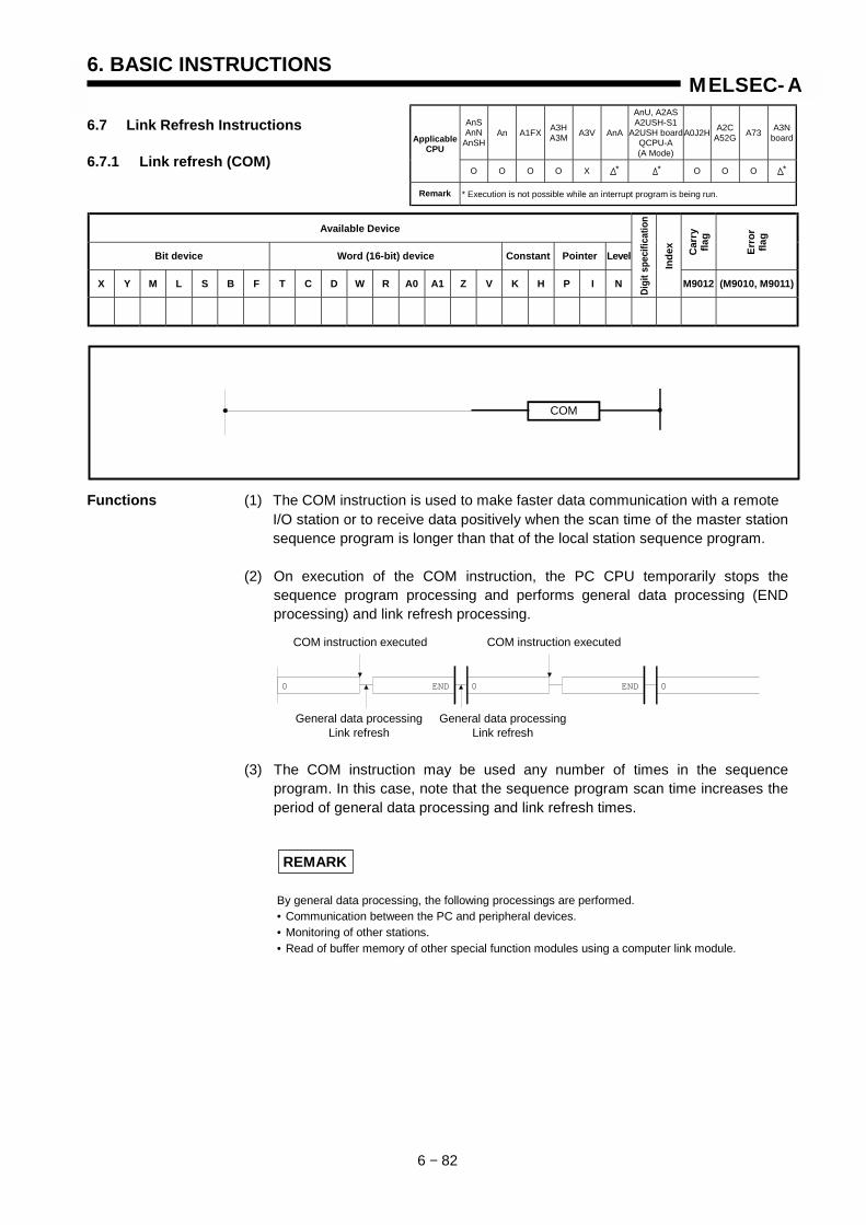
6. BASIC INSTRUCTIONS
6 − 82
MELSEC-A
6.7 Link Refresh Instructions
6.7.1 Link refresh (COM)
Available Device
Bit device Word (16-bit) device Constant Pointer Level Car
ryfla
g
Erro
rfla
g
X Y M L S B F T C D W R A0 A1 Z V K H P I N
Digi
t spe
cific
atio
n
Inde
x
M9012 (M9010, M9011)
Functions (1) The COM instruction is used to make faster data communication with a remote I/O station or to receive data positively when the scan time of the master stationsequence program is longer than that of the local station sequence program.
(2) On execution of the COM instruction, the PC CPU temporarily stops thesequence program processing and performs general data processing (ENDprocessing) and link refresh processing.
(3) The COM instruction may be used any number of times in the sequenceprogram. In this case, note that the sequence program scan time increases theperiod of general data processing and link refresh times.
REMARK
By general data processing, the following processings are performed.• Communication between the PC and peripheral devices.• Monitoring of other stations.• Read of buffer memory of other special function modules using a computer link module.
AnSAnN
AnSHAn A1FX A3H
A3M A3V AnA
AnU, A2ASA2USH-S1
A2USH boardQCPU-A(A Mode)
A0J2H A2CA52G A73 A3N
boardApplicableCPU
O O O O X O O O
Remark * Execution is not possible while an interrupt program is being run.
COM
0 END 0 END 0
COM instruction executed COM instruction executed
General data processingLink refresh
General data processingLink refresh
* * *

6. BASIC INSTRUCTIONS
6 − 83
MELSEC-A
Execution (1) Data communication using the COM instructionConditions
1) Example without using the COM instruction
2) Example using the COM instruction
3) By using the COM instruction in the master station, data communication canbe made faster as the number of data communication times with the remoteI/O station can be increased unconditionally as shown in Example 2).
4) Data may not be received as shown in Example 1) when the scan time of thelocal station sequence program is longer than that of the master stationsequence program. By using the COM instruction in the local station, datacan be received securely.
5) By using the COM instruction the local station, a link refresh is made everytime the local station receives the master station command between:
(a) Step 0 and COM instruction(b) COM instruction and COM instruction(c) COM instruction and END instruction
(2) Even if the COM instruction is used in the master station, data communicationcannot be made faster when the link scan time is longer than the master stationsequence program scan time.
0 END 0 END 0 END 0 END 0 END 0 END 0
0 END 0 END 0 END 0
Master station program
Data communication
Local station program
Remote I/O stationI/O refresh
0 END 0 END 0 END 0 END 0 END 0
0 0 END 00
COM COM COM COM COM COM
COM COM COM COM COM
END END COM COM COM END
Master station program
Data communication
Local station program
Remote I/O stationI/O refresh
0 COM END 0 COM END 0 COM END0 COM
END
Sequence programlink scan
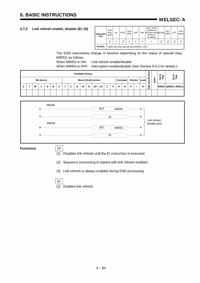
6. BASIC INSTRUCTIONS
6 − 84
MELSEC-A
6.7.2 Link refresh enable, disable (EI, DI)
The EI/DI instructions change in function depending on the status of special relayM9053, as follows.When M9053 is ON: Link refresh enable/disableWhen M9053 is OFF: Interruption enable/disable (See Section 6.5.3 for details.)
Available Device
Bit device Word (16-bit) device Constant Pointer Level Car
ryfla
g
Erro
rfla
g
X Y M L S B F T C D W R A0 A1 Z V K H P I N
Digi
t spe
cific
atio
n
Inde
x
M9012 (M9010, M9011)
Functions DI(1) Disables link refresh until the EI instruction is executed.
(2) Sequence processing is started with link refresh enabled.
(3) Link refresh is always enabled during END processing.
EI(1) Enables link refresh.
AnSAnN
AnSHAn A1FX A3H
A3M A3V AnA
AnU, A2ASA2USH-S1
A2USH boardQCPU-A(A Mode)
A0J2H A2CA52G A73 A3N
boardApplicableCPU
X X X X X
Remark * Valid only when special relay M9053 is OFF.
Link refreshdisable area
SET
DI
M9036
M9036
M9053
SET
DI
M9053
* * * ** *
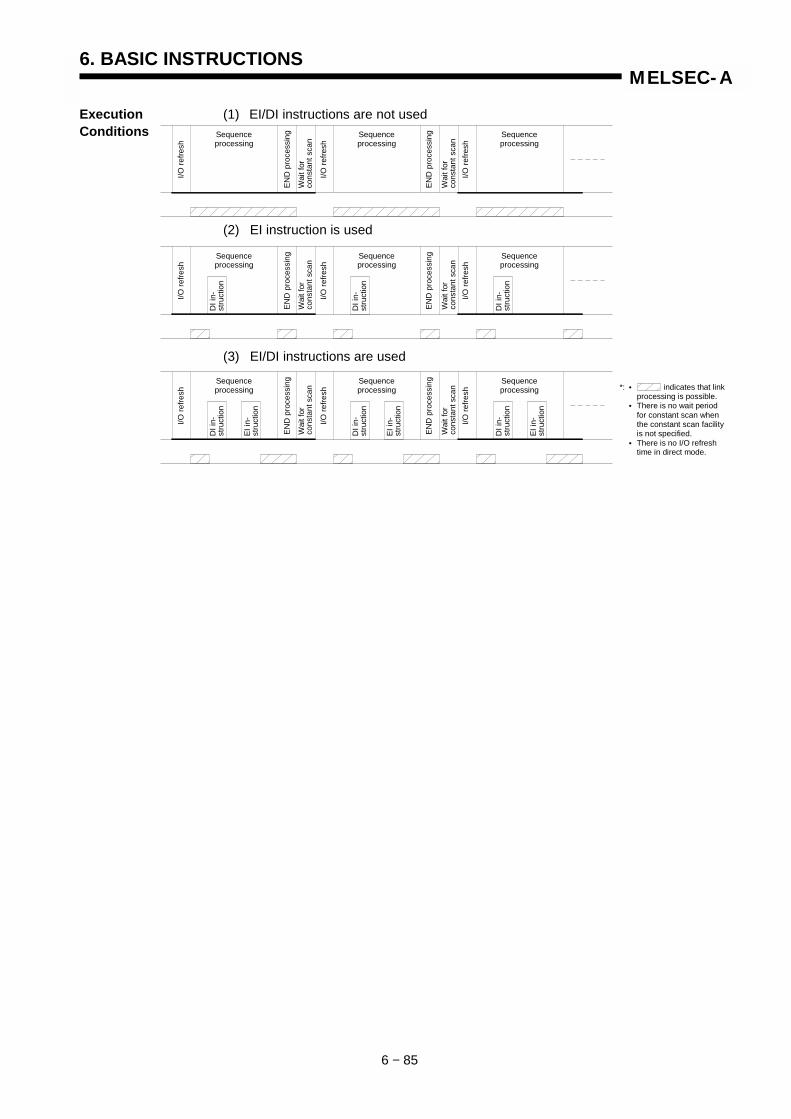
6. BASIC INSTRUCTIONS
6 − 85
MELSEC-A
Execution (1) EI/DI instructions are not usedConditions
(2) EI instruction is used
(3) EI/DI instructions are used
Sequenceprocessing
Sequenceprocessing
Sequenceprocessing
I/O re
fresh
END
pro
cess
ing
Wai
t for
cons
tant
sca
n
I/O re
fresh
END
pro
cess
ing
Wai
t for
cons
tant
sca
nI/O
refre
sh
Sequenceprocessing
Sequenceprocessing
Sequenceprocessing
I/O re
fresh
END
pro
cess
ing
Wai
t for
cons
tant
sca
n
I/O re
fresh
END
pro
cess
ing
Wai
t for
cons
tant
sca
nI/O
refre
sh
DI i
n-st
ruct
ion
DI i
n-st
ruct
ion
DI i
n-st
ruct
ion
Sequenceprocessing
Sequenceprocessing
Sequenceprocessing
I/O re
fresh
END
pro
cess
ing
Wai
t for
cons
tant
sca
n
I/O re
fresh
END
pro
cess
ing
Wai
t for
cons
tant
sca
nI/O
refre
sh
DI i
n-st
ruct
ion
DI i
n-st
ruct
ion
DI i
n-st
ruct
ion
EI in
-st
ruct
ion
EI in
-st
ruct
ion
EI in
-st
ruct
ion
*: • indicates that linkprocessing is possible.
• There is no wait period for constant scan when the constant scan facilityis not specified.
• There is no I/O refresh time in direct mode.

6. BASIC INSTRUCTIONS
6 − 86
MELSEC-A
Program Example EI , DIThe following program allows the interrupt program to be called at any time and linkrefresh to be disabled until the EI instruction is executed before the FENDinstruction is executed.
POINTS
(1) Processing is started with link refresh enabled.
(2) The interrupt program is started with interrupt disabled.
(3) After the EI/DI instruction is executed, M9053 may either be on or off.
(4) If the EI or DI instruction is contained in the MC instruction, such EI and DIare executed regardless of execution of the MC instruction.
IESET M9053DIRST M9053
RST M9053EI
SET M9053
ENDprocessing
FEND
0
Link refresh
Program
Interrupt program
M9053OFF
ON
Disable
Enable
Disable
Enable
SET M9053
EI
M9036
0
1
5
35
30
34
M9036
M9036
M9036
DI
RST M9053
EI
39 DI
SET M9053
RST M9053
Enables the interrupt programas M9053 is off.
Disables link refresh as M9053is on.
Enables link refresh as M9053is on.
6

MEMO
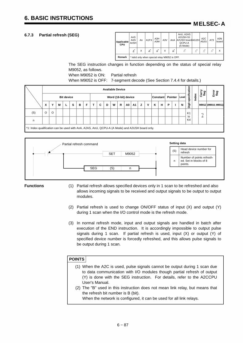
6. BASIC INSTRUCTIONS
6 − 87
MELSEC-A
6.7.3 Partial refresh (SEG)
The SEG instruction changes in function depending on the status of special relayM9052, as follows.When M9052 is ON: Partial refreshWhen M9052 is OFF: 7-segment decode (See Section 7.4.4 for details.)
Available Device
Bit device Word (16-bit) device Constant Pointer Level Car
ryfla
g
Erro
rfla
g
X Y M L S B F T C D W R A0 A1 Z V K H P I N
Digi
t spe
cific
atio
n
Inde
x
M9012 (M9010, M9011)
(S) O O
n
K1toK4
*1: Index qualification can be used with AnA, A2AS, AnU, QCPU-A (A Mode) and A2USH board only.
Functions (1) Partial refresh allows specified devices only in 1 scan to be refreshed and also allows incoming signals to be received and output signals to be output to outputmodules.
(2) Partial refresh is used to change ON/OFF status of input (X) and output (Y)during 1 scan when the I/O control mode is the refresh mode.
(3) In normal refresh mode, input and output signals are handled in batch afterexecution of the END instruction. It is accordingly impossible to output pulsesignals during 1 scan. If partial refresh is used, input (X) or output (Y) ofspecified device number is forcedly refreshed, and this allows pulse signals tobe output during 1 scan.
POINTS
(1) When the A2C is used, pulse signals cannot be output during 1 scan dueto data communication with I/O modules though partial refresh of output(Y) is done with the SEG instruction. For details, refer to the A2CCPUUser's Manual.
(2) The "B" used in this instruction does not mean link relay, but means thatthe refresh bit number is B (bit).When the network is configured, it can be used for all link relays.
AnSAnN
AnSHAn A1FX A3H
A3M A3V AnA
AnU, A2ASA2USH-S1
A2USH boardQCPU-A(A Mode)
A0J2H A2CA52G A73 A3N
boardApplicableCPU
X X X
Remark * Valid only when special relay M9052 is OFF.
* * * ** ** *
*1
SET M9052
SEG (S) n
Partial refresh command
(S) Head device number forrefresh
nNumber of points refresh-ed. Set in blocks of 8points.
Setting data

6. BASIC INSTRUCTIONS
6 − 88
MELSEC-A
Execution (1) Data must be set as shown below:Conditions
(2) Setting the head device numberThe head device number of devices to be refreshed is set. If the number is setbetween Yn0 and Yn7 (Xn0 and Xn7), refresh is done for the number of specifi-ed points from Yn0 (Xn0), and if the number is set between Yn8 and YnF (Xn8and XnF), refresh is done for the number of specified points from Yn8 (Xn8).
(3) Setting the number of points refreshedThe actual points refreshed are (set value) × 8 points and may be up to 2048points maximum.
B1 = 8 pointsB2 = 16 points
BA = 80 pointsBB = 88 points
B10 = 128 points
BFF = 2048 points
(4) Partial refresh processing is still performed if the SEG instruction is executedwith the CPU set in X/Y direct mode, but in this case, input (X)/output (Y)ON/OFF status does not change.
(5) Setting B0 (0 point) refreshes all devices in the unit, beginning with the headdevice number specified.
K4 K4SEG Y010 B001
SET M9052 Specifies partial refresh.
Set the number of pointsrefreshed in blocks of 8 points.(Valid for B only)May be any of K1, K2, K3 orK4. Function is always thesame.Set the head device number.(Valid for X, Y only)
……
……
……
……
……
……
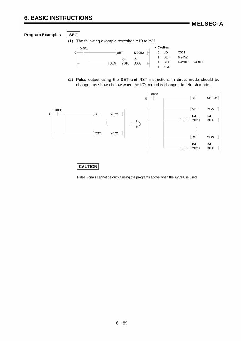
6. BASIC INSTRUCTIONS
6 − 89
MELSEC-A
Program Examples SEG(1) The following example refreshes Y10 to Y27.
(2) Pulse output using the SET and RST instructions in direct mode should bechanged as shown below when the I/O control is changed to refresh mode.
CAUTION
Pulse signals cannot be output using the programs above when the A2CPU is used.
K4 K4SEG Y010 B003
SET M9052X001
0•••• Coding
0 LD X0011 SET M90524 SEG K4Y010 K4B003
11 END
SET Y022X001
0
RST Y022
K4 K4SEG Y020 B001
SET M9052X001
0
SET Y022
K4 K4SEG Y020 B001
RST Y022

A − 4
CONTENTS
1. INTRODUCTION ......................................................................................................................1 −−−− 1 ~ 1 −−−− 3
2. INSTRUCTIONS.....................................................................................................................2 −−−− 1 ~ 2 −−−− 24
2.1 Classification...............................................................................................................................2 − 1
2.2 Instruction List.............................................................................................................................2 − 22.2.1 Explanation for instructions lists ....................................................................................2 − 22.2.2 Sequence instructions ...................................................................................................2 − 52.2.3 Basic instructions...........................................................................................................2 − 82.2.4 Application instructions ................................................................................................2 − 16
3. INSTRUCTION STRUCTURE ................................................................................................3 −−−− 1 ~ 3 −−−− 24
3.1 Instruction Structure....................................................................................................................3 − 1
3.2 Bit Processing .............................................................................................................................3 − 33.2.1 1-bit processing..............................................................................................................3 − 33.2.2 Digit specification processing ........................................................................................3 − 3
3.3 Handling of Numeric Values .......................................................................................................3 − 6
3.4 Storing 32-bit Data......................................................................................................................3 − 8
3.5 Index Qualification ....................................................................................................................3 − 103.6 Subset Processing....................................................................................................................3 − 12
3.7 Operation Error .........................................................................................................................3 − 12
3.8 Cautions on Using AnA, A2AS, AnU, QCPU-A (A Mode) and A2USH board..........................3 − 143.8.1 The number of steps used in instructions....................................................................3 − 143.8.2 Instructions of variable functions .................................................................................3 − 163.8.3 Set values for the extension timer and counter ...........................................................3 − 173.8.4 Cautions on using index qualification ..........................................................................3 − 173.8.5 Storing 32-bit data in index registers ...........................................................................3 − 20
3.9 Operation when the OUT Instruction, SET/RST Instruction andPLS/PLF Instruction are from the Same Device .........................................................................3 − 21
4. INSTRUCTION FORMAT .........................................................................................................4 −−−− 1 ~ 4 −−−− 3
5. SEQUENCE INSTRUCTIONS................................................................................................5 −−−− 4 ~ 5 −−−− 41
5.1 Contact Instructions ....................................................................................................................5 − 25.1.1 Operation start, series connection,parallel connection
(LD, LDI, AND, ANI, OR, ORI).......................................................................................5 − 25.2 Connection Instructions ..............................................................................................................5 − 5
5.2.1 Ladder block series connection, parallel connection (ANB, ORB) ................................5 − 55.2.2 Operation result push, read, pop (MPS, MRD, MPP)....................................................5 − 9
5.3 Output Instructions....................................................................................................................5 − 145.3.1 Bit device, timer, counter output (OUT) .......................................................................5 − 145.3.2 Bit device set, reset (SET,RST) ...................................................................................5 − 195.3.3 Edge-triggered differential output (PLS, PLF) .............................................................5 − 235.3.4 Bit device output reverse (CHK) ..................................................................................5 − 25

A − 5
5.4 Shift Instructions .......................................................................................................................5 − 275.4.1 Bit device shift (SFT, SFTP).........................................................................................5 − 27
5.5 Master Control Instructions.......................................................................................................5 − 295.5.1 Master control set, reset (MC, MCR)...........................................................................5 − 29
5.6 Termination Instructions............................................................................................................5 − 335.6.1 Main routine program termination (FEND) ..................................................................5 − 335.6.2 Sequence program termination (END) ........................................................................5 − 35
5.7 Other Instructions......................................................................................................................5 − 375.7.1 Sequence program stop (STOP) .................................................................................5 − 375.7.2 No operation (NOP, NOPLF) .......................................................................................5 − 39
6. BASIC INSTRUCTIONS.........................................................................................................6 −−−− 1 ~ 6 −−−− 89
6.1 Comparison Operation Instructions ............................................................................................6 − 26.1.1 16-bit data comparison (=, <>, >, <=, <, >=)..................................................................6 − 46.1.2 32-bit data comparison (D=, D<>, D>, D<=, D<,D>=) ...................................................6 − 6
6.2 Arithmetic Operation Instructions................................................................................................6 − 86.2.1 BIN 16-bit addition, subtraction (+, +P, -, -P) ...............................................................6 − 106.2.2 BIN 32-bit addition, subtraction (D+, D+P, D-, D-P).....................................................6 − 136.2.3 BIN 16-bit multiplication, division (*, *P, /, /P) ..............................................................6 − 166.2.4 BIN 32-bit multiplication, division (D*, D*P, D/, D/P)....................................................6 − 196.2.5 BCD 4-digit addition, subtraction (B+, B+P, B-, B-P) ...................................................6 − 226.2.6 BCD 8-digit addition, subtraction (DB+, DB+P, DB-, DB-P).........................................6 − 256.2.7 BCD 4-digit multiplication, division (B*, B*P, B/, B/P) ..................................................6 − 286.2.8 BCD 8-digit multiplication, division (DB*, DB*P, DB/, DB/P)........................................6 − 316.2.9 16-bit BIN data increment, decrement (INC, INCP, DEC, DECP) ...............................6 − 346.2.10 32-bit BIN data increment, decrement (DINC, DINCP, DDEC, DDECP).....................6 − 36
6.3 BCD ↔ BIN Conversion Instructions........................................................................................6 − 386.3.1 BIN data → BCD 4-, 8-digit conversion (BCD, BCDP, DBCD, DBCDP) .....................6 − 396.3.2 BCD 4-, 8-digit → BIN data conversion (BIN, BINP, DBIN, DBINP)............................6 − 42
6.4 Data Transfer Instructions.........................................................................................................6 − 466.4.1 16-, 32-bit data transfer (MOV, MOVP, DMOV, DMOVP) ............................................6 − 476.4.2 16-, 32-bit data negation transfer (CML, CMLP, DCML, DCMLP)...............................6 − 496.4.3 16-bit data block transfer (BMOV, BMOVP, FMOV, FMOVP)......................................6 − 526.4.4 16-, 32-bit data exchange (XCH, XCHP, DXCH, DXCHP) ..........................................6 − 56
6.5 Program Branch Instructions ....................................................................................................6 − 586.5.1 Conditional jump, unconditional jump (CJ, SCJ, JMP)................................................6 − 586.5.2 Subroutine call, return (CALL, CALLP, RET)...............................................................6 − 626.5.3 Interrupt enable, disable, return (EI, DI, IRET) ............................................................6 − 646.5.4 Microcomputer program call (SUB, SUBP) .................................................................6 − 67
6.6 Program Switching Instructions ................................................................................................6 − 696.6.1 Main ↔ subprogram switching (CHG).........................................................................6 − 69

A − 6
6.7 Link Refresh Instructions ..........................................................................................................6 − 826.7.1 Link refresh (COM) ......................................................................................................6 − 826.7.2 Link refresh enable, disable (EI, DI) ............................................................................6 − 846.7.3 Partial refresh (SEG) ...................................................................................................6 − 87
7. APPLICATION INSTRUCTIONS..........................................................................................7 −−−− 1 ~ 7 −−−− 133
7.1 Logical Operation Instructions ....................................................................................................7 − 27.1.1 16-, 32-bit data logical product (WAND, WANDP, DAND, DANDP) ..............................7 − 37.1.2 16-, 32-bit data logical add (WOR, WORP, DOR, DORP).............................................7 − 77.1.3 16-, 32-bit data exclusive logical add (WXOR, WXORP, DXOR, DXORP) ................. 7 − 117.1.4 16, 32-bit data NOT exclusive logical add (WXNR, WXNRP, DXNR, DXNRP)...........7 − 157.1.5 BIN 16-bit data 2’s complement (NEG, NEGP) ...........................................................7 − 19
7.2 Rotation Instructions .................................................................................................................7 − 217.2.1 16-bit data right rotation (ROR, RORP, RCR, PCRP) .................................................7 − 227.2.2 16-bit data left rotation (ROL, ROLR, RCL, RCLP) .....................................................7 − 247.2.3 32-bit data right rotation (DROR, DRORP, DRCR, DRCRP).......................................7 − 267.2.4 32-bit data left rotation (DROL, DROLP, DRCL, DRCLP) ...........................................7 − 28
7.3 Shift Instructions .......................................................................................................................7 − 307.3.1 16-bit data n-bit right shift, left shift (SFR, SFRP, SFL, SFLP) ....................................7 − 317.3.2 n-bit data 1-bit right shift, left shift (BSFR, BSFRP, BSFL, BSFLP) ............................7 − 337.3.3 n-word data 1-word right shift, left shift (DSFR, DSFRP, DSFL, DSFLP)....................7 − 35
7.4 Data Processing Instructions ....................................................................................................7 − 377.4.1 16-bit data search (SER, SERP) .................................................................................7 − 387.4.2 16-, 32-bit data bit check (SUM, SUMP, DSUM, DSUMP) ..........................................7 − 407.4.3 8 ↔ 256-bit decode, encode (DECO, DECOP, ENCO, ENCOP)................................7 − 427.4.4 7 segment decode (SEG) ............................................................................................7 − 447.4.5 Word device bit set, reset (BSET, BSETP, BRST, BRSTP) .........................................7 − 467.4.6 16-bit data dissociation, association (DIS, DISP, UNI, UNIP) .....................................7 − 487.4.7 ASCII code conversion (ASC) .....................................................................................7 − 51
7.5 FIFO Instructions ......................................................................................................................7 − 537.5.1 FIFO table write, read (FIFW, FIFWP, FIFR, FIFRP)...................................................7 − 54
7.6 Buffer Memory Access Instructions ..........................................................................................7 − 587.6.1 Special function module 1-, 2-word data read (FROM, FROMP, DFRO, DFROP) .....7 − 597.6.2 Special function module 1-, 2-word data write (TO, TOP, DTO, DTOP)......................7 − 617.6.3 Remote terminal module 1- and 2-word data read
(FROM, PRC, FROMP, PRC, DFRO, PRC, DFROP, PRC) ........................................7 − 637.6.4 Remote terminal module 1- and 2-word data write
(TO, PRC, TOP, PRC, DTO, PRC, DTOP, PRC) .........................................................7 − 677.6.5 Special module/special block 1-, 2-word data read
(FROM, FROMP, DFRO, DFROP) ..............................................................................7 − 717.6.6 Special module/special block 1-, 2-word data write (TO, TOP, DTO, DTOP)..............7 − 74
7.7 FOR to NEXT Instructions ........................................................................................................7 − 777.7.1 FOR to NEXT (FOR, NEXT)........................................................................................7 − 77

A − 7
7.8 Local, Remote I/O Station Access Instructions ........................................................................7 − 797.8.1 Local station data read, write (LRDP, LWTP) ..............................................................7 − 807.8.2 Remote I/O station data read, Write (RFRP, RTOP) ...................................................7 − 86
7.9 Display Instructions...................................................................................................................7 − 927.9.1 ASCII code print instructions (PR, PRC) .....................................................................7 − 947.9.2 ASCII code comment display instructions (LED, LEDC) ...........................................7 − 1007.9.3 Character display instructions (LEDA, LEDB) ...........................................................7 − 1037.9.4 Annunciator reset instruction (LEDR) ........................................................................7 − 105
7.10 Other Instructions....................................................................................................................7 − 1087.10.1 WDT reset (WDT, WDTP)..........................................................................................7 − 1097.10.2 Specific format failure check (CHK)........................................................................... 7 − 1117.10.3 Status latch set, reset (SLT, SLTR)............................................................................ 7 − 1177.10.4 Sampling trace set, reset (STRA, STRAR)................................................................ 7 − 1197.10.5 Carry flag set, reset (STC, CLC)................................................................................7 − 1217.10.6 Pulse regeneration instruction (DUTY)......................................................................7 − 123
7.11 Servo Program Instructions ....................................................................................................7 − 1257.11.1 Servo program start (DSFRP) ...................................................................................7 − 1267.11.2 Present position data and speed change instruction (DSFLP)..................................7 − 130
8. MICROCOMPUTER MODE ...................................................................................................8 −−−− 1 ~ 8 −−−− 16
8.1 Specifications of Microcomputer Mode.......................................................................................8 − 1
8.2 Using Utility Program ..................................................................................................................8 − 2
8.3 Using User-Written Microcomputer Programs............................................................................8 − 48.3.1 Memory map..................................................................................................................8 − 68.3.2 Data memory area address configuration .....................................................................8 − 68.3.3 Differences in operations called by microcomputer instructions
according to CPU models ..............................................................................................8 − 78.3.4 Configuration of data memory area ...............................................................................8 − 8
9. ERROR CODE LIST...............................................................................................................9 −−−− 1 ~ 9 −−−− 41
9.1 Reading Error Codes ..................................................................................................................9 − 1
9.2 Error Code List for the An, AnN, A3H, A3M, A3V, A0J2H, AnS, A2C, A73, A52G, A1FX and A3Nboard...........................................................................................................................................9 − 1
9.3 Error Code List for AnSHCPU ....................................................................................................9 − 7
9.4 Error Code List for the AnACPU...............................................................................................9 − 13
9.5 Error Code List for the AnUCPU, A2ASCPU and A2USH board .............................................9 − 229.6 Error Code List for the QCPU-A (A Mode) ...............................................................................9 − 33
APPENDICES .....................................................................................................................APP −−−− 1 ~ APP −−−− 96
APPENDIX 1 LISTS OF SPECIAL RELAYS AND SPECIAL REGISTERS ...................................APP − 1
1.1 List of Special Relays ............................................................................................................APP − 11.2 Special Relays for Link ........................................................................................................APP − 13
1.3 Special Registers .................................................................................................................APP − 16
1.4 Special Registers for Link ....................................................................................................APP − 34

A − 8
APPENDIX 2 OPERATION PROCESSING TIME........................................................................APP − 392.1 Instruction Processing Time of Small Size, Compact CPUs ...............................................APP − 412.2 Instruction Processing Time of CPUs ..................................................................................APP − 66
2.3 Instruction Processing Time of QCPU-A (A Mode)..............................................................APP − 79
APPENDIX 3 ASCII CODE TABLE...............................................................................................APP − 89APPENDIX 4 FORMATS OF PROGRAM SHEETS .....................................................................APP − 90

7. APPLICATION INSTRUCTIONS
7 − 1
MELSEC-A
7. APPLICATION INSTRUCTIONS
Application instructions are used when special processing is required. They areclassified as follows:
Classification of Application Instructions Description Ref. Page
Logical operation instruction Logical operation such as logical add and logicalproduct 7-2
Rotation instruction Rotation of specified data 7-21
Shift instruction Shift of specified data 7-30
Data processing instruction Data processing such as 16-bit data search,decode, and encode 7-37
FIFO instruction Read/write of FIFO table 7-53
Buffer memory access instruction Read/write of buffer memory in special functionmodule 7-58
FOR to NEXT instruction FOR to NEXT 7-77
Local, remote I/O station access instruction Read/write of data in local, remote I/O station 7-79
Display instruction Output of character code, indication of data on LEDdisplay 7-92
MiscellaneousInstructions which are not included in the aboveclassification, such as WDT reset and carry flag
set/reset7-108

7. APPLICATION INSTRUCTIONS
7 − 2
MELSEC-A
7.1 Logical Operation Instructions
(1) The logical operation instructions are instructions which perform the logicaloperations such as logical add and logical product.
(2) The logical operation instructions are available in the following 26 types.
Classifica-tion
InstructionSymbol Ref. Page Classifica-
tionInstruction
Symbol Ref. Page Classifica-tion
InstructionSymbol Ref. Page
WAND 7-3 WXOR 7-11 NEG 7-19
WANDP 7-3 WXORP 7-11
2’scomplement
(Sign reversal) NEGP 7-19
DAND 7-3 DXOR 7-11
Logicalproduct
DANDP 7-3
ExclusiveOR
DXORP 7-11
WOR 7-7 WXNR 7-15
WORP 7-7 WXNRP 7-15
DOR 7-7 DXNR 7-15Logical
add
DORP 7-7
ExclusiveNOR
DXNRP 7-15
REMARK
The logical operation instructions perform the following processings in units of one bit.
ExampleClassification Processing Operation Expression
A B Y
0 0 0
0 1 0
1 0 0Logical product Set to 1 only when both inputs A and B are 1. Set
to 0 otherwise. Y=A⋅B
1 1 1
0 0 0
0 1 1
1 0 1Logical add Set to 0 only when both inputs A and B are 0. Set
to 1 to 1 otherwise. Y=A+B
1 1 1
0 0 0
0 1 1
1 0 1Exclusive OR Set to 0 when inputs A and B are equal. Set to 1
when they are different. Y=A⋅B+A⋅B
1 1 0
0 0 1
0 1 0
1 0 0Exclusive NOR Set to 1 when inputs A and B are equal. Set to 0
when they are different. Y= (A+B) (A+B)
1 1 1

MEMO

7. APPLICATION INSTRUCTIONS
7 − 3
MELSEC-A
7.1.1 16-, 32-bit data logical product(WAND, WANDP, DAND, DANDP)
Available Device
Bit device Word (16-bit) device Constant Pointer Level Car
ryfla
g
Erro
rfla
g
X Y M L S B F T C D W R A0 A1 Z V K H P I N
Digi
t spe
cific
atio
n
Inde
x
M9012 (M9010, M9011)
(S) O O O O O O O O O O O O O O O O O O
(D) O O O O O O O O O O O O O O O
(S1) O O O O O O O O O O O O O O O O O O
(S2) O O O O O O O O O O O O O O O O O O
WAND
(D1) O O O O O O O O O O O O O O O
K1
to
K4
(S) O O O O O O O O O O O O O O O ODAND
(D) O O O O O O O O O O O O O
K1toK8
O O
Functions WAND(1) Performs the logical product of the 16-bit data of device specified at (D) and the
16-bit data of device specified at (S) per bit, and stores the result into thedevice specified at (D).
ApplicableCPU All CPUs
1 1 1 1 11 1 1 0 0 0 10 1 11(D)
(S) 0 0 0 0 11 0 0 0 0 1 11 0 00
(D) 0 0 0 0 11 0 0 0 0 0 10 0 00
16 bits
WANDBefore execution
After execution
(S) (D)
(S) (D)P (S)
(S1)
(S2)
(D)
Data for which logicalproduct will be performedor head number of devicewhich stores data
(D1)Head number of devicewhich will store the resultof logical product
Setting data
WAND, DAND
Indicates the instruction symbol.
Operation commands
(S1) (D1)
(S1) (D1)P
(S2)
(S2) WAND may only be used in theareas marked *.
Operation commands
*
*
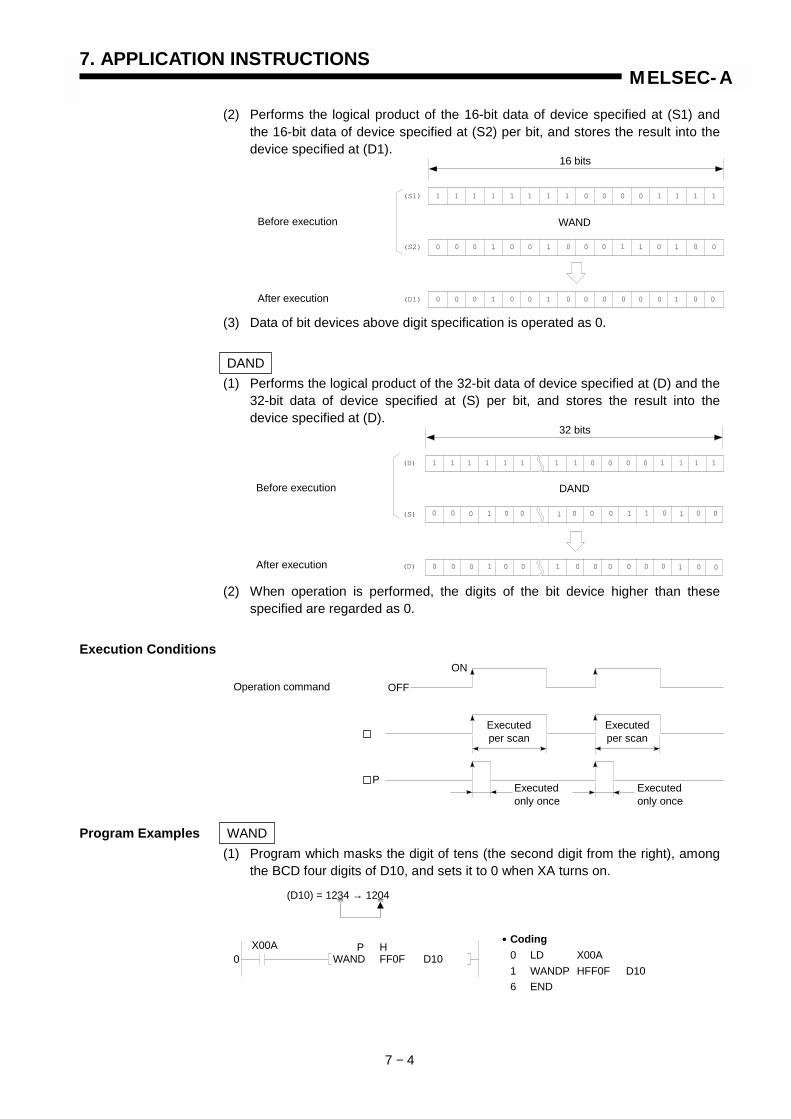
7. APPLICATION INSTRUCTIONS
7 − 4
MELSEC-A
(2) Performs the logical product of the 16-bit data of device specified at (S1) andthe 16-bit data of device specified at (S2) per bit, and stores the result into thedevice specified at (D1).
(3) Data of bit devices above digit specification is operated as 0.
DAND(1) Performs the logical product of the 32-bit data of device specified at (D) and the
32-bit data of device specified at (S) per bit, and stores the result into thedevice specified at (D).
(2) When operation is performed, the digits of the bit device higher than thesespecified are regarded as 0.
Execution Conditions
Program Examples WAND(1) Program which masks the digit of tens (the second digit from the right), among
the BCD four digits of D10, and sets it to 0 when XA turns on.
(S1) 1 1 1 1 11 1 1 0 0 0 10 1 11
(S2) 0 0 0 0 11 0 0 0 0 1 11 0 00
(D1) 0 0 0 0 11 0 0 0 0 0 10 0 00
16 bits
WANDBefore execution
After execution
(D) 1 1 1 1 11 1 1 0 0 0 10 1 11
(S) 0 0 0 0 11 0 0 0 0 1 11 0 00
(D) 0 0 0 0 11 0 0 0 0 0 10 0 00
32 bits
DANDBefore execution
After execution
OFF
ON
Executedper scan
Executedper scan
Executedonly once
Executedonly once
P
Operation command
(D10) = 1234 → 1204
X00A0
P HWAND FF0F D10
•••• Coding0 LD X00A1 WANDP HFF0F D106 END

7. APPLICATION INSTRUCTIONS
7 − 5
MELSEC-A
(2) Program which performs logical product of the data of X10 to 1B and the dataof D33, and outputs the result to the Y30 to 3B when XA turns on.
(3) Program which performs logical product of the data of X10 to 1B and the dataof D33, and sends the result to the Y30 to 3B when XA turns on.
X00A0
P K3WAND X010 D33
P K3MOV D33 Y030
Logical product of the data of X10 to 1B and thedata of D33 is performed and the result is storedinto D33.
Data of D33 is output to the Y30 to 3F.
•••• Coding0 LD X00A1 WANDP K3X010 D336 MOVP D33 K3Y030
11 END
D33 0 0 0 0 1 0 1 0 0 0 0 0 1
X1B to 10 0 0 0 0 1 0 1 0 1 0 1 0 1 0 1 0
1 1 1
b15 b14 b13 b12
0 1 1 1 0 0 0 0 0 1 0 0 0
b11 b10 b9 b8 b7 b6 b5 b4 b3 b2 b1 b0
D33
WAND
X1B X1A X19 X18 X17 X16 X15 X14 X13 X12 X11 X10
0 0 0
Regarded as 0.
Set to 0.
X00A0
P K3 K3WAND X010 D33 Y030
•••• Coding0 LD X00A1 WANDP K3X010 D33 K3Y0308 END
Y3B to 30
X1B to 10 0 0 0 0 1 0 0 1 0 0 1 1 0 0 1 1
1 1 1
b15 b14 b13 b12
0 1 0 1 1 0 0 1 0 1 0 0 1
b11 b10 b9 b8 b7 b6 b5 b4 b3 b2 b1 b0
D33
WAND
X1B X1A X19 X18 X17 X16 X15 X14 X13 X12 X11 X10
1 0 0 1 1 0 0 1 0 0 1 0 0 0 0 1
Y3B Y3A Y39 Y38 Y37 Y36 Y35 Y34 Y33 Y32 Y31 Y30
Regarded as 0.
Do not change.
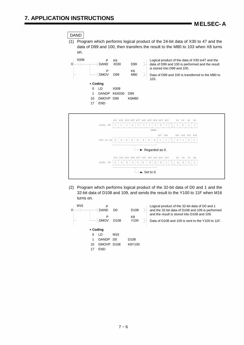
7. APPLICATION INSTRUCTIONS
7 − 6
MELSEC-A
DAND(1) Program which performs logical product of the 24-bit data of X30 to 47 and the
data of D99 and 100, then transfers the result to the M80 to 103 when X8 turnson.
(2) Program which performs logical product of the 32-bit data of D0 and 1 and the32-bit data of D108 and 109, and sends the result to the Y100 to 11F when M16turns on.
X0080
P K6DAND X030 D99
P K6DMOV D99 M80
Logical product of the data of X30 to47 and thedata of D99 and 100 is performed and the resultis stored into D99 and 100.
Data of D99 and 100 is transferred to the M80 to103.
•••• Coding0 LD X0081 DANDP K6X030 D99
10 DMOVP D99 K6M8017 END
D100, 99
D100, 99
X47 to 30
DAND
1 1 1 0
0
1
0 0
1 1 1 1
1
0 1 1 0 1 1
0 0 0 0 0 1 1 0 1 0 1
0 0 0 0 0 0 0 0 0 0 0 0
b31 b30 b29 b28 b27 b26 b25 b24 b23 b22 b3 b2 b1 b0
X47 X46 X33 X32 X31 X30
b31 b30 b29 b28 b27 b26 b25 b24 b23 b22 b3 b2 b1 b0
Regarded as 0.
Set to 0.
M160
PDAND D0 D108
P K8DMOV D108 Y100
Logical product of the 32-bit data of D0 and 1and the 32-bit data of D108 and 109 is performedand the result is stored into D108 and 109.
Data of D108 and 109 is sent to the Y100 to 11F.
•••• Coding0 LD M161 DANDP D0 D108
10 DMOVP D108 K8Y10017 END
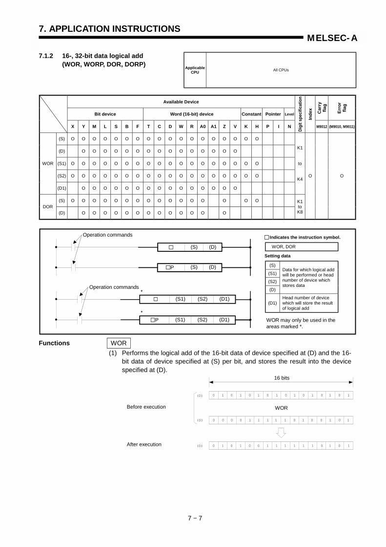
7. APPLICATION INSTRUCTIONS
7 − 7
MELSEC-A
7.1.2 16-, 32-bit data logical add(WOR, WORP, DOR, DORP)
Available Device
Bit device Word (16-bit) device Constant Pointer Level Car
ryfla
g
Erro
rfla
g
X Y M L S B F T C D W R A0 A1 Z V K H P I N
Digi
t spe
cific
atio
n
Inde
x
M9012 (M9010, M9011)
(S) O O O O O O O O O O O O O O O O O O
(D) O O O O O O O O O O O O O O O
(S1) O O O O O O O O O O O O O O O O O O
(S2) O O O O O O O O O O O O O O O O O O
WOR
(D1) O O O O O O O O O O O O O O O
K1
to
K4
(S) O O O O O O O O O O O O O O O ODOR
(D) O O O O O O O O O O O O O
K1toK8
O O
Functions WOR(1) Performs the logical add of the 16-bit data of device specified at (D) and the 16-
bit data of device specified at (S) per bit, and stores the result into the devicespecified at (D).
ApplicableCPU All CPUs
(S) (D)
(S) (D)P (S)
(S1)
(S2)
(D)
Data for which logical addwill be performed or headnumber of device whichstores data
(D1)Head number of devicewhich will store the resultof logical add
Setting data
WOR, DOR
Indicates the instruction symbol.
Operation commands
(S1) (D1)
(S1) (D1)P
(S2)
(S2) WOR may only be used in theareas marked *.
Operation commands
*
*
(D) 0 1 0 1 01 0 1 0 1 0 11 0 10
(S) 0 0 0 1 10 1 1 1 0 1 10 0 10
(D) 0 1 0 0 11 0 1 1 1 1 11 0 10
16 bits
WORBefore execution
After execution

7. APPLICATION INSTRUCTIONS
7 − 8
MELSEC-A
(2) Performs the logical add of the 16-bit data of device specified at (S1) and the16-bit data of device specified at (S2) per bit, and stores the result into thedevice specified at (D1).
(3) Data of bit devices above digit specification is operated as 0.
DOR(1) Performs the logical add of the 32-bit data of device specified at (D) and the 32-
bit data of device specified at (S) per bit, and stores the result into the devicespecified at (D).
(2) When operation is performed, the digits of bit device higher than the specifiedare regarded as 0.
Execution Conditions
(S1) 0 1 0 1 01 0 1 0 1 0 11 0 10
(S2) 0 0 0 1 10 1 1 1 0 1 10 0 10
(D1) 0 1 0 0 11 0 1 1 1 1 11 0 10
16 bits
WORBefore execution
After execution
(D)
(S) 0 0
(D)
0
1
0 1
1 1
1
0 1 01 0 1 01 0 1 1 0 1
0 0 1 1 0 1 0 0 1 0 1
0 1 0 1 0 1 0 11 1 1 11 1 1
32 bits
DORBefore execution
After execution
OFF
ON
Executedper scan
Executedper scan
Executedonly once
Executedonly once
P
Operation command

7. APPLICATION INSTRUCTIONS
7 − 9
MELSEC-A
Program Examples WOR(1) Program which performs logical add of the data of D10 and that of D20, and
stores the result to D10 when XA turns on.
(2) Program which performs logical add of the data of X10 to 1B and the data ofD33, and sends the result to the Y30 to 3F when XA turns on.
(3) Program which performs logical add of the data of D10 and that of D20, andstores the result to D33 when XA turns on.
(4) Program which performs logical add of the data of X10 to 1B and the data ofD33, and sends the result to the Y30 to 3B when XA turns on.
X00A0
PWOR D20 D10
•••• Coding0 LD X00A1 WORP D20 D106 END
X00A0
P K3WOR X010 D33
P K4MOV D33 Y030
Logical add of the data of X10 to 1B and the dataof D33 is performed and the result is stored intoD33.
Data of D33 is sent to the Y30 to 3F.
•••• Coding0 LD X00A1 WORP K3X010 D336 MOVP D33 K4Y030
11 END
X00A0
PWOR D10 D20 D33
•••• Coding0 LD X00A1 WORP D10 D20 D338 END
X00A0
P K3 K3WOR X010 D33 Y030
•••• Coding0 LD X00A1 WORP K3X010 D33 K3Y0308 END

7. APPLICATION INSTRUCTIONS
7 − 10
MELSEC-A
DOR(1) Program which performs logical add of the 32-bit data of X0 to 1F and the
hexadecimal number of F0FFH and stores the result to D66 and 67 when XBturns on.
(2) Program which performs logical add of the 24-bit data of M64 to 87 and the 24-bit data of X20 to 37 and stores the result to D23 and 24 when M8 turns on.
X0080
P HDMOV 0000F0FF D66
P K8DOR X000 D66
Hexadecimal number of F0FFH is stored into D66and 67.
Logical add of the 32-bit data of X0 to 1F and the32-bit data of D66 and 67 is performed and theresult is stored into D66 and 67.
•••• Coding0 LD X00B1 DMOVP H0000F0FF D668 DORP K8X000 D66
17 END
M80
P K6DMOV X020 D23
P K6DOR M64 D23
24-bit data of X20 to 37 is stored into D23 and 24.
Logical add of the 24-bit data of M64 to 87 andthe 24-bit data of D23 is performed and the resultis stored into D23 and 24.
•••• Coding0 LD M81 DMOVP K6X020 D238 DORP K6M64 D23
17 END

7. APPLICATION INSTRUCTIONS
7 − 11
MELSEC-A
7.1.3 16-, 32-bit data exclusive logical add(WXOR, WXORP, DXOR, DXORP)
Available Device
Bit device Word (16-bit) device Constant Pointer Level Car
ryfla
g
Erro
rfla
g
X Y M L S B F T C D W R A0 A1 Z V K H P I N
Digi
t spe
cific
atio
n
Inde
x
M9012 (M9010, M9011)
(S) O O O O O O O O O O O O O O O O O O
(D) O O O O O O O O O O O O O O O
(S1) O O O O O O O O O O O O O O O O O O
(S2) O O O O O O O O O O O O O O O O O O
WXOR
(D1) O O O O O O O O O O O O O O O
K1
to
K4
(S) O O O O O O O O O O O O O O O ODXOR
(D) O O O O O O O O O O O O O
K1toK8
O O
Functions WXOR(1) Performs the exclusive OR of the 16-bit data of device specified at (D) and the
16-bit data of device specified at (S) per bit, and stores the result into thedevice specified at (D).
ApplicableCPU All CPUs
(S) (D)
(S) (D)P (S)
(S1)
(S2)
(D)
Data for which exclusiveOR will be performed orhead number of devicewhich stores data
(D1)Head number of devicewhich will store the resultof exclusive OR
Setting data
WXOR, DXOR
Indicates the instruction symbol.
Operation commands
(S1) (D1)
(S1) (D1)P
(S2)
(S2) WXOR may only be used in theareas marked *.
Operation commands
*
*
(D) 0 1 0 1 01 0 1 0 1 0 11 0 10
(S) 0 0 0 1 10 1 1 0 0 0 10 1 11
(D) 0 1 0 0 11 1 0 0 1 0 01 1 01
16 bits
WXORBefore execution
After execution
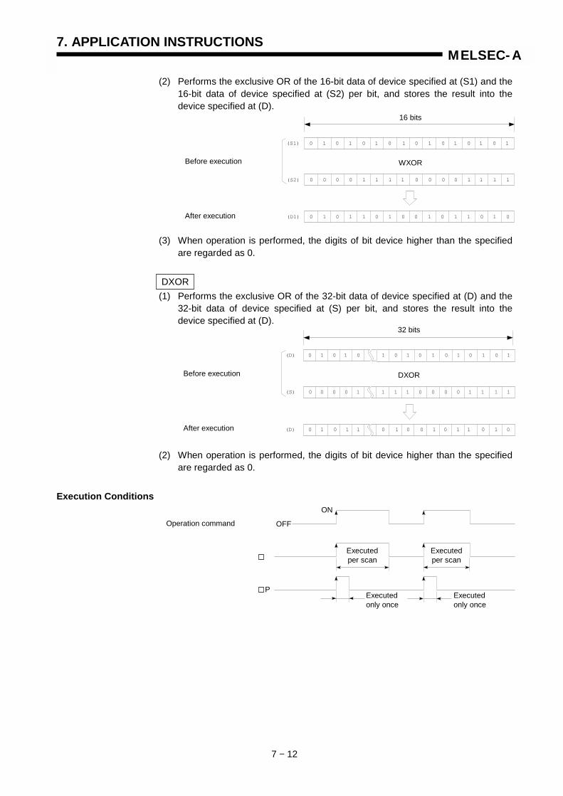
7. APPLICATION INSTRUCTIONS
7 − 12
MELSEC-A
(2) Performs the exclusive OR of the 16-bit data of device specified at (S1) and the16-bit data of device specified at (S2) per bit, and stores the result into thedevice specified at (D).
(3) When operation is performed, the digits of bit device higher than the specifiedare regarded as 0.
DXOR(1) Performs the exclusive OR of the 32-bit data of device specified at (D) and the
32-bit data of device specified at (S) per bit, and stores the result into thedevice specified at (D).
(2) When operation is performed, the digits of bit device higher than the specifiedare regarded as 0.
Execution Conditions
(S1) 0 1 0 1 01 0 1 0 1 0 11 0 10
(S2) 0 0 0 1 10 1 1 0 0 0 10 1 11
(D1) 0 1 0 0 11 1 0 0 1 0 01 1 01
16 bits
WXORBefore execution
After execution
(D)
(S) 0 0
(D)
0
1
0 1
1 1
1
0 1 01 0 1 01 0 1 1 0 1
0 0 1 0 0 0 0 1 1 1 1
0 1 0 1 1 0 1 00 1 0 10 1 0
32 bits
DXORBefore execution
After execution
OFF
ON
Executedper scan
Executedper scan
Executedonly once
Executedonly once
P
Operation command
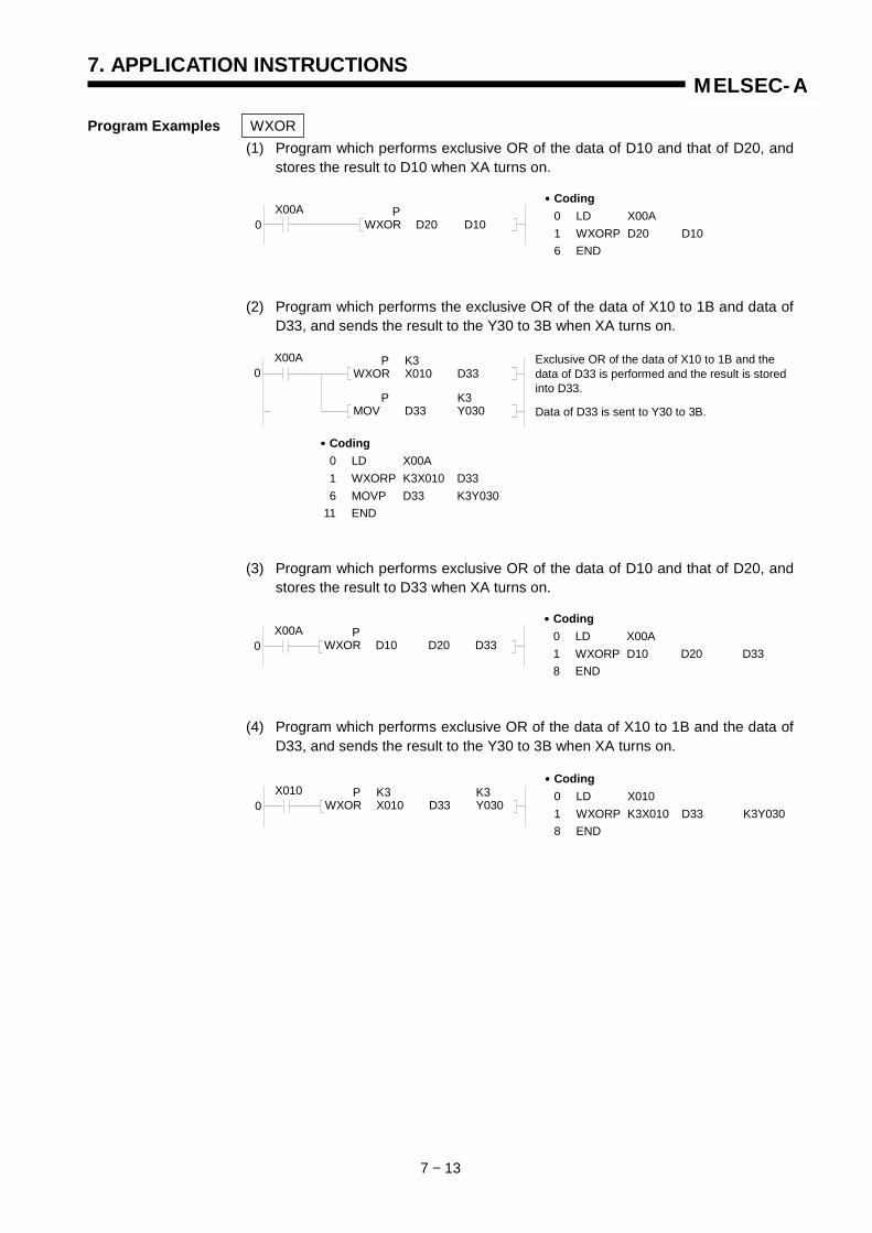
7. APPLICATION INSTRUCTIONS
7 − 13
MELSEC-A
Program Examples WXOR(1) Program which performs exclusive OR of the data of D10 and that of D20, and
stores the result to D10 when XA turns on.
(2) Program which performs the exclusive OR of the data of X10 to 1B and data ofD33, and sends the result to the Y30 to 3B when XA turns on.
(3) Program which performs exclusive OR of the data of D10 and that of D20, andstores the result to D33 when XA turns on.
(4) Program which performs exclusive OR of the data of X10 to 1B and the data ofD33, and sends the result to the Y30 to 3B when XA turns on.
X00A0
PWXOR D20 D10
•••• Coding0 LD X00A1 WXORP D20 D106 END
X00A0
P K3WXOR X010 D33
P K3MOV D33 Y030
Exclusive OR of the data of X10 to 1B and thedata of D33 is performed and the result is storedinto D33.
Data of D33 is sent to Y30 to 3B.
•••• Coding0 LD X00A1 WXORP K3X010 D336 MOVP D33 K3Y030
11 END
X00A0
PWXOR D10 D20 D33
•••• Coding0 LD X00A1 WXORP D10 D20 D338 END
X0100
P K3 K3WXOR X010 D33 Y030
•••• Coding0 LD X0101 WXORP K3X010 D33 K3Y0308 END

7. APPLICATION INSTRUCTIONS
7 − 14
MELSEC-A
DXOR(1) Program which compares the 32-bit data of X20 to 3F and the bit pattern of
data of D9 and 10, and stores the number of different bits to D16 when X6 turnson.
X0060
P K8DXOR X020 D9
PDSUM D9
Exclusive OR of the 32-bit data of X20 to 3F andthe data of D9 and 10 is performed.
Comparing 32-bit data of D9 and 10, the totalnumber of "1" bits is stored into A0.
•••• Coding0 LD X0061 DXORP K8X020 D9
10 DSUMP D913 MOVP A0 D1618 END
PMOV A0 D16 Data of A0 is stored into D16.
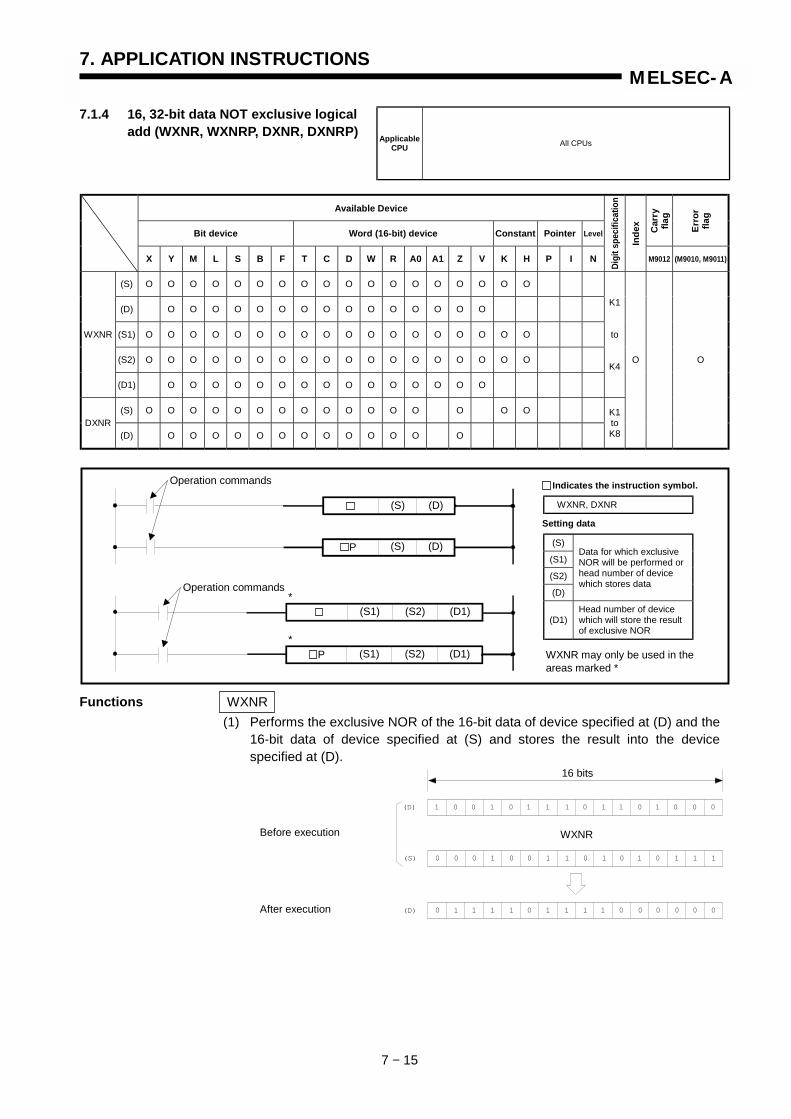
7. APPLICATION INSTRUCTIONS
7 − 15
MELSEC-A
7.1.4 16, 32-bit data NOT exclusive logicaladd (WXNR, WXNRP, DXNR, DXNRP)
Available Device
Bit device Word (16-bit) device Constant Pointer Level Car
ryfla
g
Erro
rfla
g
X Y M L S B F T C D W R A0 A1 Z V K H P I N
Digi
t spe
cific
atio
n
Inde
x
M9012 (M9010, M9011)
(S) O O O O O O O O O O O O O O O O O O
(D) O O O O O O O O O O O O O O O
(S1) O O O O O O O O O O O O O O O O O O
(S2) O O O O O O O O O O O O O O O O O O
WXNR
(D1) O O O O O O O O O O O O O O O
K1
to
K4
(S) O O O O O O O O O O O O O O O ODXNR
(D) O O O O O O O O O O O O O
K1toK8
O O
Functions WXNR(1) Performs the exclusive NOR of the 16-bit data of device specified at (D) and the
16-bit data of device specified at (S) and stores the result into the devicespecified at (D).
ApplicableCPU All CPUs
(S) (D)
(S) (D)P (S)
(S1)
(S2)
(D)
Data for which exclusiveNOR will be performed orhead number of devicewhich stores data
(D1)Head number of devicewhich will store the resultof exclusive NOR
Setting data
WXNR, DXNR
Indicates the instruction symbol.
Operation commands
(S1) (D1)
(S1) (D1)P
(S2)
(S2) WXNR may only be used in theareas marked *
Operation commands
*
*
(D) 1 0 0 1 11 0 1 0 1 1 00 1 00
(S) 0 0 0 0 11 0 1 0 1 0 11 0 11
(D) 0 1 1 0 11 1 1 1 1 0 00 0 00
16 bits
WXNRBefore execution
After execution

7. APPLICATION INSTRUCTIONS
7 − 16
MELSEC-A
(2) Performs the exclusive NOR of the 16-bit data of device specified at (S1) andthe 16-bit data of device specified at (S2) and stores the result into the devicespecified at (D).
(3) When operation is performed, the digits of bit device higher than the specifiedare regarded as 0.
DXNR(1) Performs the exclusive NOR of the 32-bit data of device specified at (D) and the
32-bit data of device specified at (S) and stores the result into the devicespecified at (D).
(2) When operation is performed, the digits of bit device higher than the specifiedare regarded as0.
Execution Conditions
POINT
The DXNR instruction in the AnA, A2AS, AnU, QCPU-A (A Mode) and A2USHboard dedicated instructions changes to the 32-bit constant setting instruction.For details, refer to the AnSHCPU/AnACPU/AnUCPU Programming Manual(Dedicated Instructions).
(S1) 1 0 0 1 11 0 1 0 1 1 00 1 00
(S2) 0 0 0 0 11 0 1 0 1 0 11 0 11
(D1) 0 1 1 0 11 1 1 1 1 0 00 0 00
16 bits
WXNRBefore execution
After execution
(D)
(S) 1 0
(D)
1 1
1 0
0 0 11 0 0 0 0 1
1 0 1 0 1 0 1
1 0 0 1 0 0 1 11 1 0
32 bits
WXNRBefore execution
After execution
OFF
ON
Executedper scan
Executedper scan
Executedonly once
Executedonly once
P
Operation command
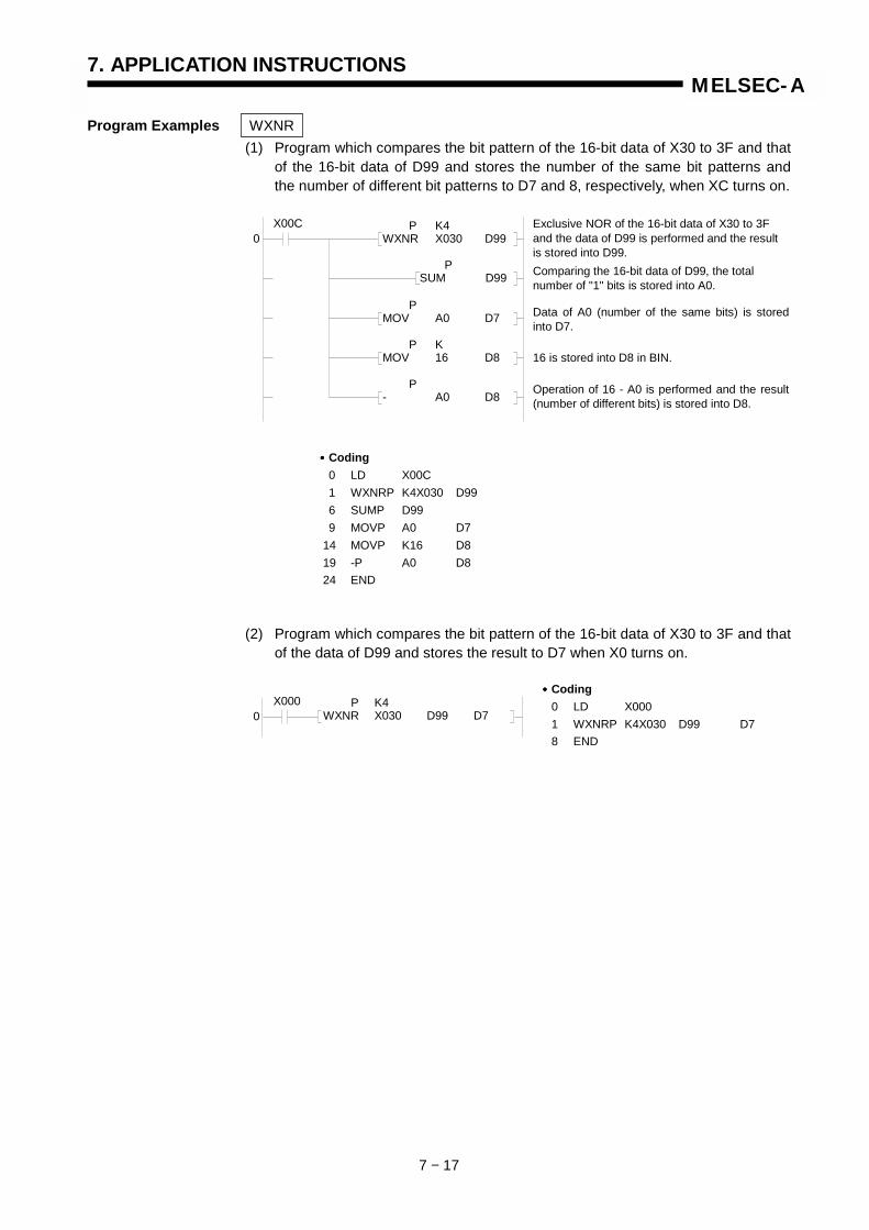
7. APPLICATION INSTRUCTIONS
7 − 17
MELSEC-A
Program Examples WXNR(1) Program which compares the bit pattern of the 16-bit data of X30 to 3F and that
of the 16-bit data of D99 and stores the number of the same bit patterns andthe number of different bit patterns to D7 and 8, respectively, when XC turns on.
(2) Program which compares the bit pattern of the 16-bit data of X30 to 3F and thatof the data of D99 and stores the result to D7 when X0 turns on.
X00C0
PSUM D99
Exclusive NOR of the 16-bit data of X30 to 3Fand the data of D99 is performed and the resultis stored into D99.Comparing the 16-bit data of D99, the totalnumber of "1" bits is stored into A0.
•••• Coding0 LD X00C1 WXNRP K4X030 D996 SUMP D999 MOVP A0 D7
14 MOVP K16 D819 -P A0 D824 END
Data of A0 (number of the same bits) is storedinto D7.
P K4WXNR X030 D99
PMOV A0 D7
P KMOV 16 D8
P- A0 D8 Operation of 16 - A0 is performed and the result
(number of different bits) is stored into D8.
16 is stored into D8 in BIN.
X0000
P K4WXNR X030 D99 D7
•••• Coding0 LD X0001 WXNRP K4X030 D99 D78 END

7. APPLICATION INSTRUCTIONS
7 − 18
MELSEC-A
DXNR(1) Program which compares the bit pattern of the 32-bit data of X20 to 3F and that
of the data of D16 and 17, and stores the number of the same bit patterns toD18 when X6 turns on.
X0060
P K8DXNR X020 D16
PDSUM D16
Exclusive NOR of the 32-bit data of X20 to 3Fand the data of D16 and 17 is performed.
Among 32-bit data of D16 and 17, the totalnumber of "1" bits is stored into A0.
•••• Coding0 LD X0061 DXNRP K8X020 D16
10 DSUMP D1613 MOVP A0 D1818 END
PMOV A0 D18 Data of A0 is stored into D18.

7. APPLICATION INSTRUCTIONS
7 − 19
MELSEC-A
7.1.5 BIN 16-bit data 2’s complement(NEG, NEGP)
Available Device
Bit device Word (16-bit) device Constant Pointer Level Car
ryfla
g
Erro
rfla
g
X Y M L S B F T C D W R A0 A1 Z V K H P I N
Digi
t spe
cific
atio
n
Inde
x
M9012 (M9010, M9011)
(D) O O O O O O O O O O O O O O O O O
Functions (1) Reverses the sign of the 16-bit data of device specified at (D) and stores theresult in device specified at (D).
(2) Used to reverse the positive sign to the negative sign and vice versa.
Execution Conditions
ApplicableCPU All CPUs
K1 toK4
(D)
Head number of devicewhich stores data forwhich 2’s complement willbe performed
Setting data
2’s complement execution commands
(D)NEG
(D)NEGP
OFFON
Executedper scan
Executedper scan
Executedonly once
Executedonly once
NEG
NEGP
2’s complementexecution command
1 0 1 0 10 1 0 1 0 1 00 1 01
0 0 0 0 00 0 0 0 0 0 00 0 00
1 0 1 0 10 1 0 1 0 1 00 1 01
1
00 1 0 10 1 0 1 0 1 00 1 11
16 bits
-21846
21846
…………………
………………….
Before execution (D)
After execution (D)
Sign conversion
-
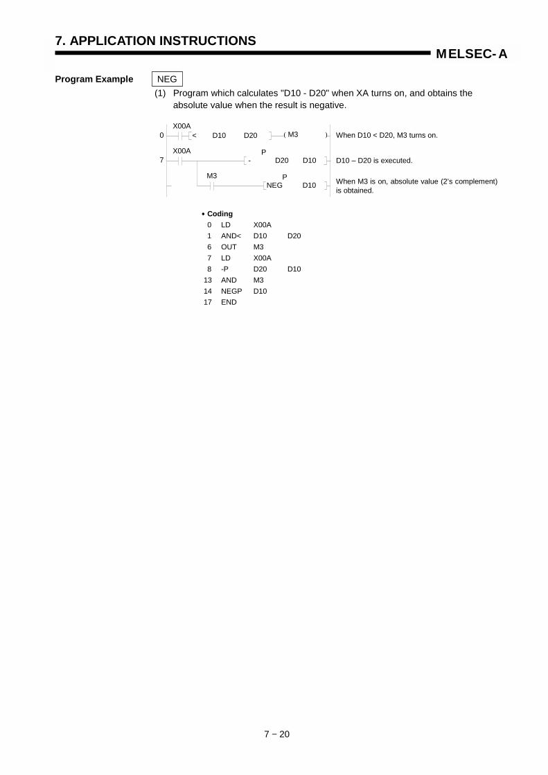
7. APPLICATION INSTRUCTIONS
7 − 20
MELSEC-A
Program Example NEG(1) Program which calculates "D10 - D20" when XA turns on, and obtains the
absolute value when the result is negative.
( )X00A
0 < D10 D20
P- D20 D10
When D10 < D20, M3 turns on.
D10 – D20 is executed.
•••• Coding0 LD X00A1 AND< D10 D206 OUT M37 LD X00A8 -P D20 D10
13 AND M314 NEGP D1017 END
PNEG D10 When M3 is on, absolute value (2’s complement)
is obtained.
M3
X00A7
M3
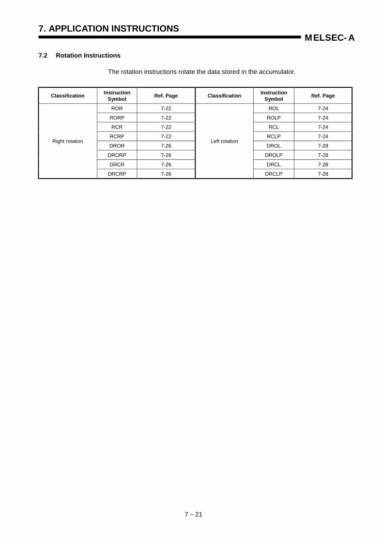
7. APPLICATION INSTRUCTIONS
7 − 21
MELSEC-A
7.2 Rotation Instructions
The rotation instructions rotate the data stored in the accumulator.
Classification InstructionSymbol Ref. Page Classification Instruction
Symbol Ref. Page
ROR 7-22 ROL 7-24
RORP 7-22 ROLP 7-24
RCR 7-22 RCL 7-24
RCRP 7-22 RCLP 7-24
DROR 7-26 DROL 7-28
DRORP 7-26 DROLP 7-28
DRCR 7-26 DRCL 7-28
Right rotation
DRCRP 7-26
Left rotation
DRCLP 7-28

MEMO
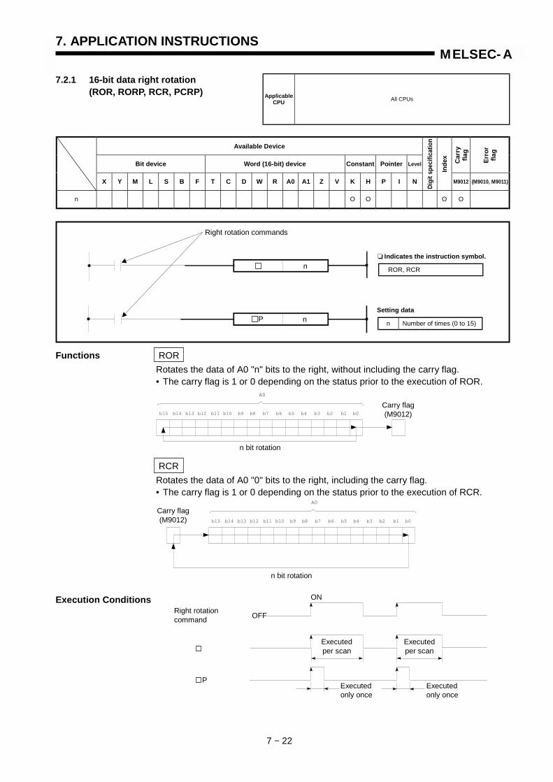
7. APPLICATION INSTRUCTIONS
7 − 22
MELSEC-A
7.2.1 16-bit data right rotation(ROR, RORP, RCR, PCRP)
Available Device
Bit device Word (16-bit) device Constant Pointer Level Car
ryfla
g
Erro
rfla
g
X Y M L S B F T C D W R A0 A1 Z V K H P I N
Digi
t spe
cific
atio
n
Inde
x
M9012 (M9010, M9011)
n O O O O
Functions RORRotates the data of A0 "n" bits to the right, without including the carry flag.• The carry flag is 1 or 0 depending on the status prior to the execution of ROR.
RCRRotates the data of A0 "0" bits to the right, including the carry flag.• The carry flag is 1 or 0 depending on the status prior to the execution of RCR.
Execution Conditions
ApplicableCPU All CPUs
A0
b15 b14 b13 b12 b11 b10 b9 b8 b7 b6 b5 b3 b2 b1 b0b4
Carry flag(M9012)
n bit rotation
A0
b15 b14 b13 b12 b11 b10 b9 b8 b7 b6 b5 b3 b2 b1 b0b4
Carry flag(M9012)
n bit rotation
ON
OFF
Executedper scan
Executedper scan
Executedonly once
Executedonly once
Right rotationcommand
P
Right rotation commands
n
n
ROR, RCR
❏ Indicates the instruction symbol.
n Number of times (0 to 15)
Setting dataP
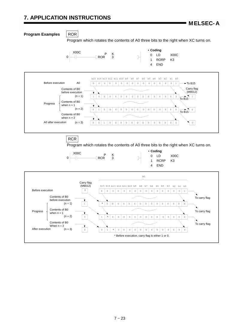
7. APPLICATION INSTRUCTIONS
7 − 23
MELSEC-A
Program Examples RORProgram which rotates the contents of A0 three bits to the right when XC turns on.
RCRProgram which rotates the contents of A0 three bits to the right when XC turns on.
X00C P KROR 30
• Coding0 LD X00C1 RORP K34 END
X00C P KRCR 30
• Coding0 LD X00C1 RCRP K34 END
0 0 0 0 1
0 0 00
1 0
b15 b14 b13 b10 b9b12 b11 b8 b7 b6 b5 b2b4 b3 b0b1
0 0 0 0 0 0 0 0 0 0 0
0 0 0 0 0 0 0 0 0 0 0
000 0 0 0 0 0 0 0 0 0 0
0 1 000 0 0 0 0 0 0 0 0 0 0
1
0
0
A0
*
*
*
*
To carry flag
To carry flag
To carry flag
* Before execution, carry flag is either 1 or 0.
Carry flag(M9012)
Contents of B0before execution
(n = 1)
Contents of B0when n = 1
(n = 2)
Contents of B0When n = 2
(n = 3)After execution
Before execution
Progress
0 0 0 0 1
1 0 0 00
0 1 0
b15 b14 b13 b10 b9b12 b11 b8 b7 b6 b5 b2b4 b3 b0b1
0 0 0 0 0 0 0 0 0 0 0
0 0 0 0 0 0 0 0 0 0 0
000 0 0 0 0 0 0 0 0 0 0
0 0 1 000 0 0 0 0 0 0 0 0 0 0
1
0
0
To B15
To B15
Carry flag(M9012)
To B15
Contents of B0before execution
A0
(n = 1)
Contents of B0when n = 1
(n = 2)
Contents of B0when n = 2
(n = 3)
Before execution
A0 after execution
Progress

7. APPLICATION INSTRUCTIONS
7 − 24
MELSEC-A
7.2.2 16-bit data left rotation(ROL, ROLR, RCL, RCLP)
Available Device
Bit device Word (16-bit) device Constant Pointer Level Car
ryfla
g
Erro
rfla
g
X Y M L S B F T C D W R A0 A1 Z V K H P I N
Digi
t spe
cific
atio
n
Inde
x
M9012 (M9010, M9011)
n O O O O
Functions ROLRotates the data of A0 "n" bits to the left, without including the carry flag.• The carry flag is 1 or 0 depending on the status prior to the execution of ROL.
RCLRotates the data of A0 "0" bits to the left, including the carry flag.• The carry flag is 1 or 0 depending on the status prior to the execution of RCL.
Execution Conditions
ApplicableCPU All CPUs
Left rotation commands
n
n
ROL, RCL
❏ Indicates the instruction symbol.
n Number of times (0 to 15)
Setting dataP
Carry flag(M9012)
A0
b15 b14 b13 b12 b11 b10 b9 b8 b7 b6 b5 b3 b2 b1 b0b4
n bit rotation
A0
b15 b14 b13 b12 b11 b10 b9 b8 b7 b6 b5 b3 b2 b1 b0b4
Carry flag(M9012)
n bit rotation
OFF
Executedper scan
Executedper scan
Executedonly once
Executedonly once
Left rotation command
P
ON
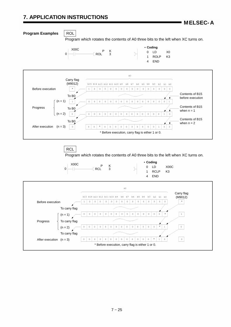
7. APPLICATION INSTRUCTIONS
7 − 25
MELSEC-A
Program Examples ROLProgram which rotates the contents of A0 three bits to the left when XC turns on.
RCLProgram which rotates the contents of A0 three bits to the left when XC turns on.
0 0 0 0 0
0 0 0 10
0 0 0
b15 b14 b13 b10 b9b12 b11 b8 b7 b6 b5 b2b4 b3 b0b1
1 0 0 0 0 0 0 0 0 0 0
0 0 0 0 0 0 0 0 0 0 0
010 0 0 0 0 0 0 0 0 0 0
0 0 000 0 0 0 0 0 0 0 0 0 1
1
0
0
A0
*
*
Contents of B15before execution
Contents of B15when n = 1
Contents of B15when n = 2
Carry flag(M9012)
To B0
To B0
To B0
(n = 1)
(n = 2)
(n = 3)
Before execution
Progress
After execution
* Before execution, carry flag is either 1 or 0.
0 0 0 0 0
0 0 0 0
0 0 0
b15 b14 b13 b10 b9b12 b11 b8 b7 b6 b5 b2b4 b3 b0b1
1 0 0 0 0 0 0 0 0 0 0
0 0 0 0 0 0 0 0 0 0 0
10 0 0 0 0 0 0 0 0 0 0
0 0 0 010 0 0 0 0 0 0 0 0 0
1
0
0
A0
*
*
*
*
X00C P KROL 30
• Coding0 LD X01 ROLP K34 END
X00C P KRCL 30
• Coding0 LD X00C1 RCLP K34 END
Carry flag(M9012)
* Before execution, carry flag is either 1 or 0.
To carry flag
To carry flag
To carry flag
(n = 1)
(n = 2)
(n = 3)After execution
Progress
Before execution
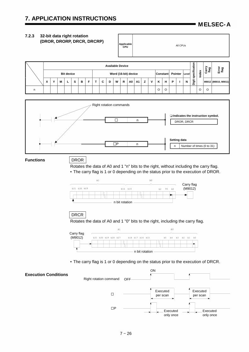
7. APPLICATION INSTRUCTIONS
7 − 26
MELSEC-A
7.2.3 32-bit data right rotation(DROR, DRORP, DRCR, DRCRP)
Available Device
Bit device Word (16-bit) device Constant Pointer Level Car
ryfla
g
Erro
rfla
g
X Y M L S B F T C D W R A0 A1 Z V K H P I N
Digi
t spe
cific
atio
n
Inde
x
M9012 (M9010, M9011)
n O O O O
Functions DRORRotates the data of A0 and 1 "n" bits to the right, without including the carry flag.• The carry flag is 1 or 0 depending on the status prior to the execution of DROR.
DRCRRotates the data of A0 and 1 "0" bits to the right, including the carry flag.
• The carry flag is 1 or 0 depending on the status prior to the execution of DRCR.
Execution Conditions
ApplicableCPU All CPUs
Right rotation commands
n
n
DROR, DRCR
❏ Indicates the instruction symbol.
n Number of times (0 to 31)
Setting dataP
OFF
Executedper scan
Executedper scan
Executedonly once
Executedonly once
Right rotation command
P
ON
Carry flag(M9012)
A0
b31 b30 b29 b16 b15 b2 b1 b0
A1
n bit rotation
A0
b31 b30 b29 b16 b15 b2 b1 b0
A1
b28 b27 b18 b17 b5 b4 b3
Carry flag(M9012)
n bit rotation

7. APPLICATION INSTRUCTIONS
7 − 27
MELSEC-A
Program Examples DRORProgram which rotates the contents of A0 and 1 three bits to the right when XC turnson.
DRCRProgram which rotates the contents of A0 and 1 three bits to the right when XC turnson.
P KDMOV 1 A0
X00A
X00C P KDROR 3
0
8
• Coding0 LD X00A1 DMOVP K1 A08 LD X00C9 DRORP K3
12 END
P KDMOV 1 A0
X00A
X00C P KDRCR 3
0
8
• Coding0 LD X00A1 DMOVP K1 A08 LD X00C9 DRCRP K3
12 END
0 0 1
0 0 00
1 0
b31 b30 b16 b15 b4 b1b5 b2b3
0 0 0 0 0
0 0 0
000 0 0 0
0 1 0 0 0 0
0 0
00
0
0 0 0
b0
A1 A0
1
0
0
*
*
*
*
Contents of B0before execution
(n = 1)
Contents of B0when n = 1
(n = 2)
Contents of B0when n = 2
(n = 3)
Before execution
After execution
Progress
To carry flag
To carry flag
To carry flag
* Before execution, carry flag is either 1 or 0.
Carry flag(M9012)
0 0 0 1
1 0 0 00
0 1 0
b31 b30 b29 b17b28 b27 b16 b15 b14 b13 b4 b1b5 b2b3
0 0 0 0 0 0 0 0 0 0
0 0 0 0 0 0 0 0 0
000 0 0 0 0 0 0 0 0 0
0 0 1 0 0 0 0 0 0 0 0 0 0
1
0
0
0 0
00
0
0 0 0
b0
A1 A0
Contents of B0before execution
(n = 1)
Contents of B0when n = 1
(n = 2)
Contents of B0when n = 2
(n = 3)
Before execution
After execution
Progress
To B31
To B31
To B31
Carry flag (M9012)
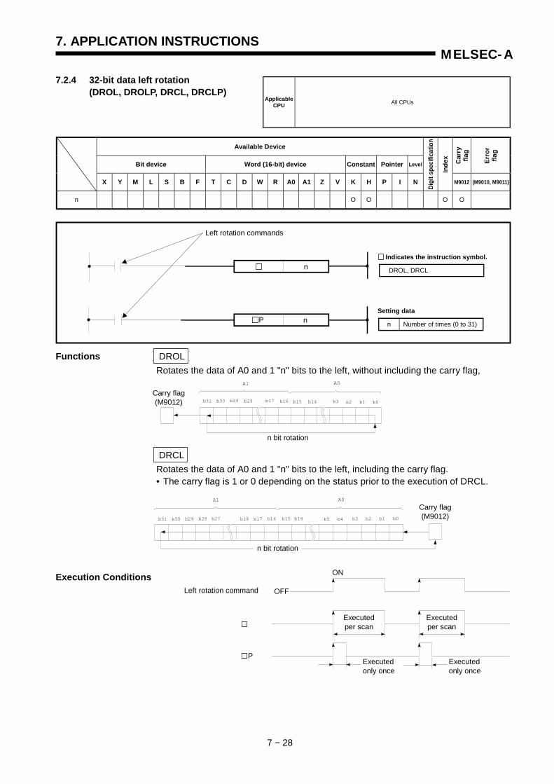
7. APPLICATION INSTRUCTIONS
7 − 28
MELSEC-A
7.2.4 32-bit data left rotation(DROL, DROLP, DRCL, DRCLP)
Available Device
Bit device Word (16-bit) device Constant Pointer Level Car
ryfla
g
Erro
rfla
g
X Y M L S B F T C D W R A0 A1 Z V K H P I N
Digi
t spe
cific
atio
n
Inde
x
M9012 (M9010, M9011)
n O O O O
Functions DROLRotates the data of A0 and 1 "n" bits to the left, without including the carry flag,
DRCLRotates the data of A0 and 1 "n" bits to the left, including the carry flag.• The carry flag is 1 or 0 depending on the status prior to the execution of DRCL.
Execution Conditions
ApplicableCPU All CPUs
Left rotation commands
n
n
DROL, DRCL
Indicates the instruction symbol.
n Number of times (0 to 31)
Setting dataP
OFF
Executedper scan
Executedper scan
Executedonly once
Executedonly once
Left rotation command
P
ON
Carry flag(M9012)
A0
b31 b30 b29 b15 b14 b0
A1
b28 b17 b16 b3 b2 b1
n bit rotation
b1b5 b4 b3
A0
b31 b30 b29 b16 b15
A1
b28 b27 b18 b17 b14 b2 b0
Carry flag(M9012)
n bit rotation

7. APPLICATION INSTRUCTIONS
7 − 29
MELSEC-A
Program Examples DROLProgram which rotates the contents of A0 and 1 three bits to the left when XC turnson.
DRCLProgram which rotates the contents of A0 and 1 three bits to the left when XC turnson.
P HDMOV 80000000 A0
X00A
X00C P KDROL 3
0
8
• Coding0 LD X00A1 DMOVP H80000000 A08 LD X00C9 DROLP K3
12 END
0
0 0 0
0 0 0
b31 b30 b29 b16b28 b27 b15 b14 b1b2
1 0 0 0 0 0 0
0 0 0 0
0 0 0
0 0 0 0 0
b0
A1 A0
1
0
0
00 0 1
0 0 0
00 0 0 1 0
000 01
Carry flag(M9012)
Contents ofB31 beforeexecution
Contents ofB31 whenn = 1
Contents ofB31 whenn = 2
To B0
(n = 1)
(n = 2)
(n = 3)
To B0
To B0
Prog
ress
Beforeexecution
Afterexecution
P HDMOV 80000000 A0
X00A
X00C P KDRCL 3
0
8
• Coding0 LD X00A1 DMOVP H80000000 A08 LD X00C9 DRCLP K3
12 END
0
0 0 0
0 0 0
b31 b30 b29 b16b28 b27 b15 b1b2
0 0 0 0 0 0
0 0 0
0 0
0 0 0 0
b0
A1 A0
00 0 *
0 0 0
00 0 0 * 1
000 1*
0
0
1
0
b26
1
0
0
*
* Before execution, carry flag is either 1 or 0.
To carry flag
To carry flag
To carry flag
(n = 1)
(n = 2)
(n = 3)Afterexecution
Before execution
Prog
ress
Carry flag(M9012)
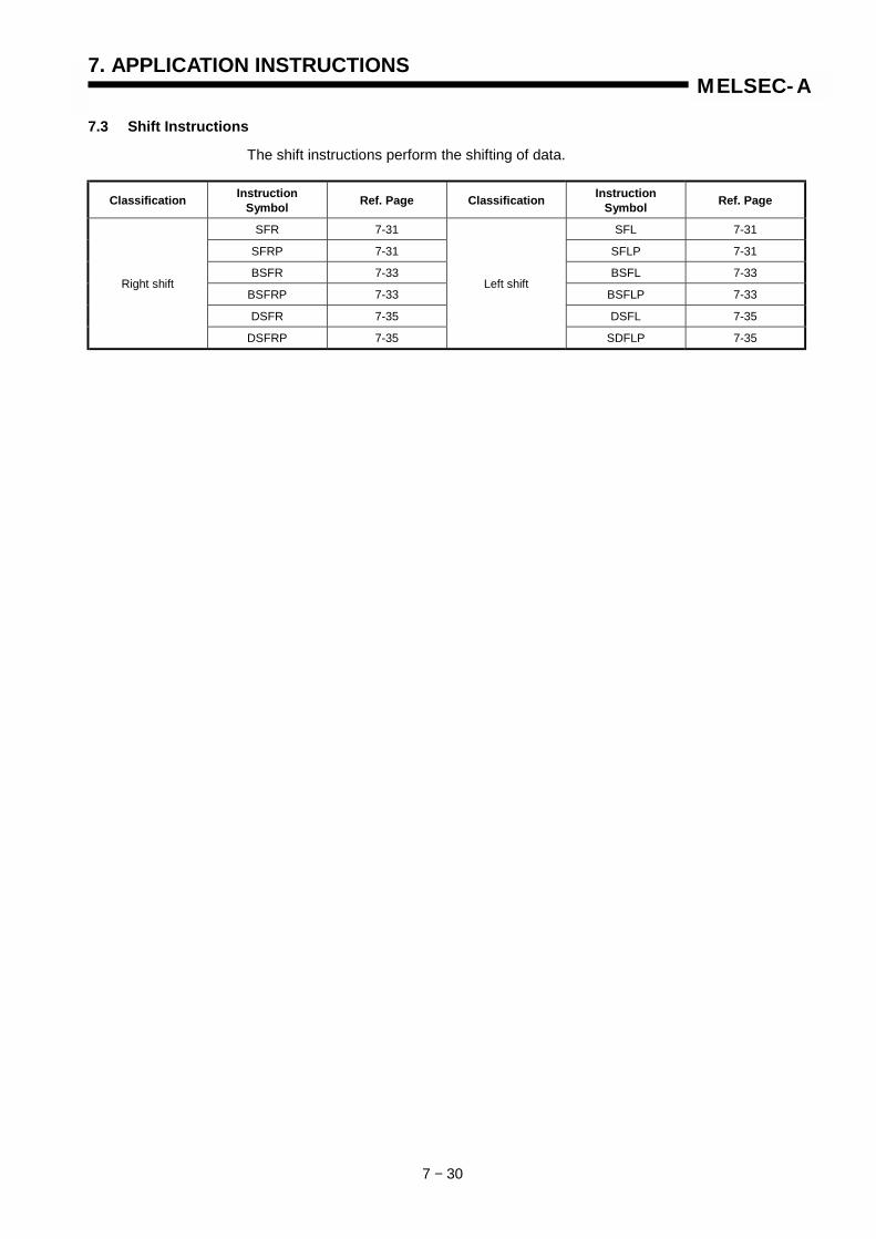
7. APPLICATION INSTRUCTIONS
7 − 30
MELSEC-A
7.3 Shift Instructions
The shift instructions perform the shifting of data.
Classification InstructionSymbol Ref. Page Classification Instruction
Symbol Ref. Page
SFR 7-31 SFL 7-31
SFRP 7-31 SFLP 7-31
BSFR 7-33 BSFL 7-33
BSFRP 7-33 BSFLP 7-33
DSFR 7-35 DSFL 7-35
Right shift
DSFRP 7-35
Left shift
SDFLP 7-35

MEMO
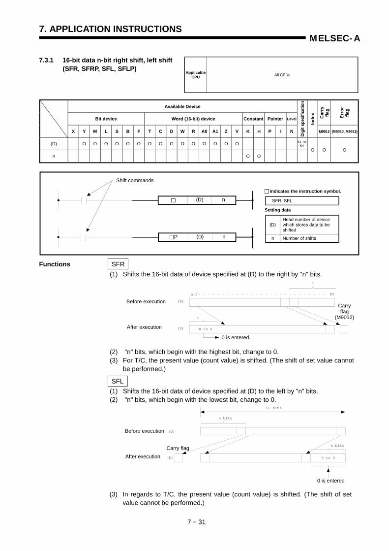
7. APPLICATION INSTRUCTIONS
7 − 31
MELSEC-A
7.3.1 16-bit data n-bit right shift, left shift(SFR, SFRP, SFL, SFLP)
Available Device
Bit device Word (16-bit) device Constant Pointer Level Car
ryfla
g
Erro
rfla
g
X Y M L S B F T C D W R A0 A1 Z V K H P I N
Digi
t spe
cific
atio
n
Inde
x
M9012 (M9010, M9011)
(D) O O O O O O O O O O O O O O O
n O OO O O
Functions SFR(1) Shifts the 16-bit data of device specified at (D) to the right by "n" bits.
(2) "n" bits, which begin with the highest bit, change to 0.(3) For T/C, the present value (count value) is shifted. (The shift of set value cannot
be performed.)
SFL(1) Shifts the 16-bit data of device specified at (D) to the left by "n" bits.(2) "n" bits, which begin with the lowest bit, change to 0.
ApplicableCPU All CPUs
K1 toK4
(D) n
(D) nP
Shift commands
(D)Head number of devicewhich stores data to beshifted
n Number of shifts
Setting data
SFR, SFL
Indicates the instruction symbol.
(D)
n bits
n bits
0 to 0
16 bits
(D) Before execution
After executionCarry flag
0 is entered
(3) In regards to T/C, the present value (count value) is shifted. (The shift of setvalue cannot be performed.)
(D)
0 to 0(D)
b15 b0
n
n
Carryflag
(M9012)
Before execution
After execution
0 is entered.
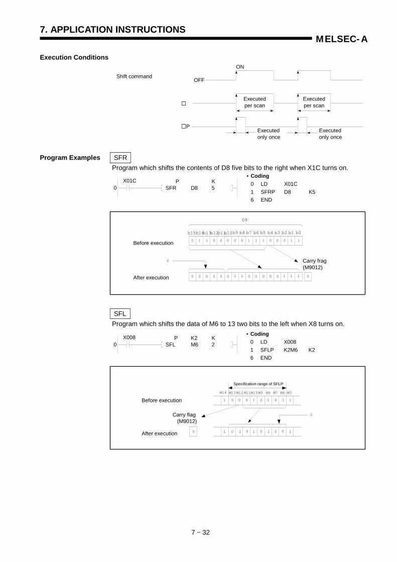
7. APPLICATION INSTRUCTIONS
7 − 32
MELSEC-A
Execution Conditions
Program Examples SFRProgram which shifts the contents of D8 five bits to the right when X1C turns on.
SFLProgram which shifts the data of M6 to 13 two bits to the left when X8 turns on.
OFF
ON
Executedper scan
Executedper scan
Executedonly once
Executedonly once
P
Shift command
• Coding0 LD X01C1 SFRP D8 K56 END
0X01C P K
SFR D8 5
• Coding0 LD X0081 SFLP K2M6 K26 END
0X008 P K2 K
SFL M6 2
Before execution
After execution 0
1
0 0 0 0 0 1 1 0 0 0 0 0 1 1 1 0
0 1 0 0 0 0 0 1 1 1 0 0 0 1 1
D8
0
b15b14b13b12b11b10b9 b8 b7 b6 b5 b4 b3 b2 b1 b0
Carry frag(M9012)
Before execution
After execution
Carry flag (M9012)
Specification range of SFLP
1 0 01 1
1 0 1
0 1 1
1 01 01 00
0 0
0
0
M14 M13M12M11M10M9 M8 M7 M6 M5
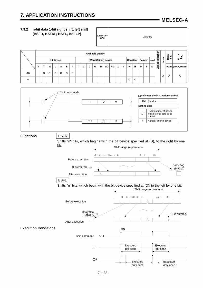
7. APPLICATION INSTRUCTIONS
7 − 33
MELSEC-A
7.3.2 n-bit data 1-bit right shift, left shift(BSFR, BSFRP, BSFL, BSFLP)
Available Device
Bit device Word (16-bit) device Constant Pointer Level Car
ryfla
g
Erro
rfla
g
X Y M L S B F T C D W R A0 A1 Z V K H P I N
Digi
t spe
cific
atio
n
Inde
x
M9012 (M9010, M9011)
(D) O O O O O O
n O OO O O
Functions BSFRShifts "n" bits, which begins with the bit device specified at (D), to the right by onebit.
BSFLShifts "n" bits, which begin with the bit device specified at (D), to the left by one bit.
Execution Conditions
ApplicableCPU All CPUs
(D) n
(D) nP
Shift commands
(D)Head number of devicewhich stores data to beshifted
n Number of shift device
Setting data
BSFR, BSFL
Indicates the instruction symbol.
OFF
ON
Executedper scan
Executedper scan
Executedonly once
Executedonly once
P
Shift command
(D)+(n- 1) (D)+(n- 2) (D)+1 (D)
Shift range (n points)
0 is entered. Carry fra(M9012)
0
Before execution
After execution
Shift range (n points)
0 is entered. Carry flag(M9012)
(D)+(n- 1)(D)+(n- 2)
0
(D)+1 (D)
Shift range (n points)
0 is entereCarry frag(M9012)
Before execution
After execution
Carry flag(M9012) 0 is entered.
Shift range (n points)
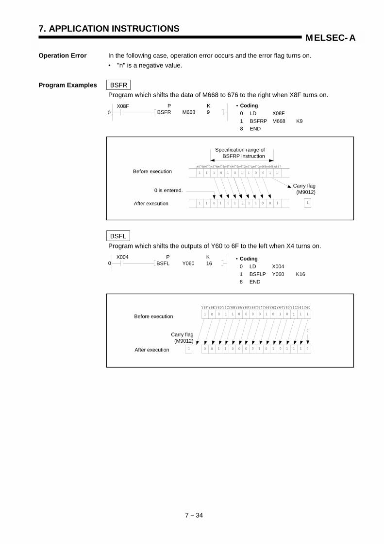
7. APPLICATION INSTRUCTIONS
7 − 34
MELSEC-A
Operation Error In the following case, operation error occurs and the error flag turns on.• "n" is a negative value.
Program Examples BSFRProgram which shifts the data of M668 to 676 to the right when X8F turns on.
BSFLProgram which shifts the outputs of Y60 to 6F to the left when X4 turns on.
Specification range ofBSFRP instruction
Before execution
After execution
0 is entered.Carry flag
(M9012)
1 0 0
1
1 1
1 0 1 1
1 1 1 0 0 1 1
1 1 0 1 0 1 0 0
M678M677M676M675M674M673M672M671M670M669M668M667
Before execution
After execution
Carry flag(M9012)
0
1
0 00 01 1 0 0 01 1 1
0 10 00 0 0 11 10 0 1 1
0
1
1
0 1 1
Y6FY6EY6DY6CY6BY6AY69Y68Y67Y66Y65Y64Y63Y62Y61Y60
X08F • Coding0 LD X08F1 BSFRP M668 K98 END
P KBSFR M668 90
X004 • Coding0 LD X0041 BSFLP Y060 K168 END
0P K
BSFL Y060 16
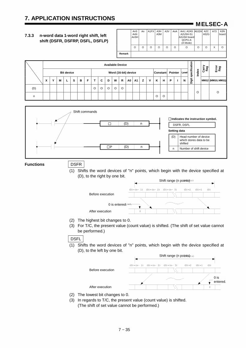
7. APPLICATION INSTRUCTIONS
7 − 35
MELSEC-A
7.3.3 n-word data 1-word right shift, leftshift (DSFR, DSFRP, DSFL, DSFLP)
Available Device
Bit device Word (16-bit) device Constant Pointer Level Car
ryfla
g
Erro
rfla
g
X Y M L S B F T C D W R A0 A1 Z V K H P I N
Digi
t spe
cific
atio
n
Inde
x
M9012 (M9010, M9011)
(D) O O O O O
n O OO O
Functions DSFR(1) Shifts the word devices of "n" points, which begin with the device specified at
(D), to the right by one bit.
(2) The highest bit changes to 0.(3) For T/C, the present value (count value) is shifted. (The shift of set value cannot
be performed.)
DSFL(1) Shifts the word devices of "n" points, which begin with the device specified at
(D), to the left by one bit.
(2) The lowest bit changes to 0.(3) In regards to T/C, the present value (count value) is shifted.
(The shift of set value cannot be performed.)
(D) n
(D) nP
Shift commands
(D) Head number of devicewhich stores data to beshifted
n Number of shift device
Setting data
DSFR, DSFL
Indicates the instruction symbol.
0
(D)+(n- 1) (D)+(n- 2) (D)+(n- 3) (D)+2 (D)+1 (D)
Shift range (n points)
0 is entered.
Before execution
After execution
Shift range (n points)
0 is entered.
(D)+(n- 1) (D)+(n- 2) (D)+(n- 3) (D)+2 (D)+1 (D)
Shift range (n points)
0
0 is entered
Before execution
After execution
Shift range (n points)
0 isentered.
AnSAnN
AnSH
An A1FX A3HA3M
A3V AnA AnU, A2ASA2USH-S1
A2USH boardQCPU-A(A Mode)
A0J2H A2CA52G
A73 A3Nboard
O O O O O O O O O X O
Remark

7. APPLICATION INSTRUCTIONS
7 − 36
MELSEC-A
Execution Conditions
Operation Error In the following case, operation error occurs and the error flag turns on.• "n" is a negative value.
Program Examples DSFRProgram which shifts the contents of D683 to 689 to the right when XB turns on.
DSFLProgram which shifts the contents of D683 to 689 to the left when XB turns on.
OFF
ON
Executedper scan
Executedper scan
Executedonly once
Executedonly once
P
Shift command
• Coding0 LD X00B1 DSFRP D683 K78 END
0X00B P K
DSFR D683 7
0X00B • Coding
0 LD X00B1 DSFLP D683 K78 END
P KDSFL D683 7
0
D688D689 D687 D686 D685 D684 D683
600 -336 3802 -32765 5003
0 -100 503 600 -336 3802 -32765
-100 503Before execution
After execution
Specification range of DSFRP instruction
Before execution
After execution
Specification range of DSFRP instruction
D688D689 D687 D686 D685 D684 D683
600 -336 3802 -32765 5003
503
503-100
600 -336 3802 -32765 5003 0
0
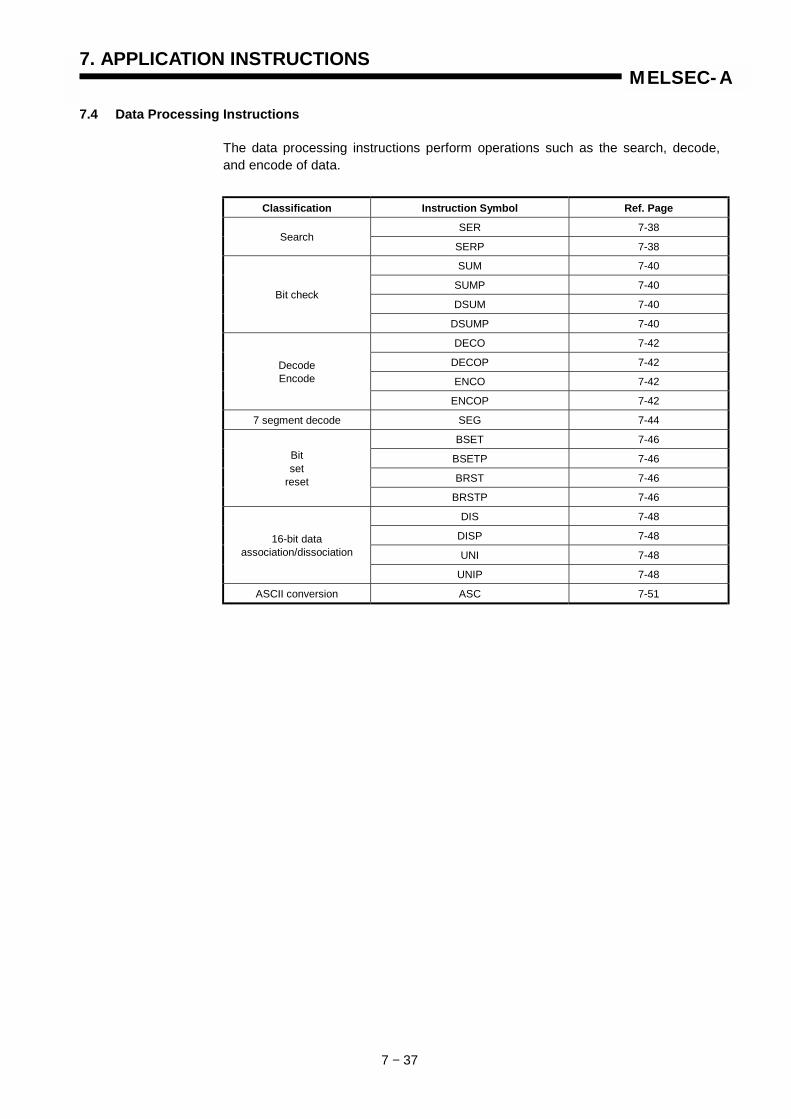
7. APPLICATION INSTRUCTIONS
7 − 37
MELSEC-A
7.4 Data Processing Instructions
The data processing instructions perform operations such as the search, decode,and encode of data.
Classification Instruction Symbol Ref. Page
SER 7-38Search
SERP 7-38
SUM 7-40
SUMP 7-40
DSUM 7-40Bit check
DSUMP 7-40
DECO 7-42
DECOP 7-42
ENCO 7-42DecodeEncode
ENCOP 7-42
7 segment decode SEG 7-44
BSET 7-46
BSETP 7-46
BRST 7-46
Bitset
resetBRSTP 7-46
DIS 7-48
DISP 7-48
UNI 7-4816-bit data
association/dissociation
UNIP 7-48
ASCII conversion ASC 7-51

MEMO

7. APPLICATION INSTRUCTIONS
7 − 38
MELSEC-A
7.4.1 16-bit data search(SER, SERP)
Available Device
Bit device Word (16-bit) device Constant Pointer Level Car
ryfla
g
Erro
rfla
g
X Y M L S B F T C D W R A0 A1 Z V K H P I N
Digi
t spe
cific
atio
n
Inde
x
M9012 (M9010, M9011)
(S1) O O O O O O O O O O O
(S2) O O O O O
n O O
O O
Functions (1) Searches the data of "n" points, beginning with the 16-bit data of devicespecified at (S2), by use of the 16-bit data of device specified at (S1) as akeyword.
(2) Stores to A1 the number of data which have coincided with the keyword, andstores to A0 at which point from (S2) the first coinciding device number (relativevalue) is located.
(3) When "n" is negative, it is equal to 0.
(4) When "n" is 0, no processing is performed.
Execution Conditions
ApplicableCPU All CPUs
(S1) Device number whichstores data to be searched
(S2) Head number of device tobe searched
n Number of devices to besearched
Setting dataSearch commands
SER (S1) (S2) n
SERP (S1) (S2) n
OFF
ON
Executedper scan
Executedper scan
Executedonly once
Executedonly once
Search command
SER
SERP
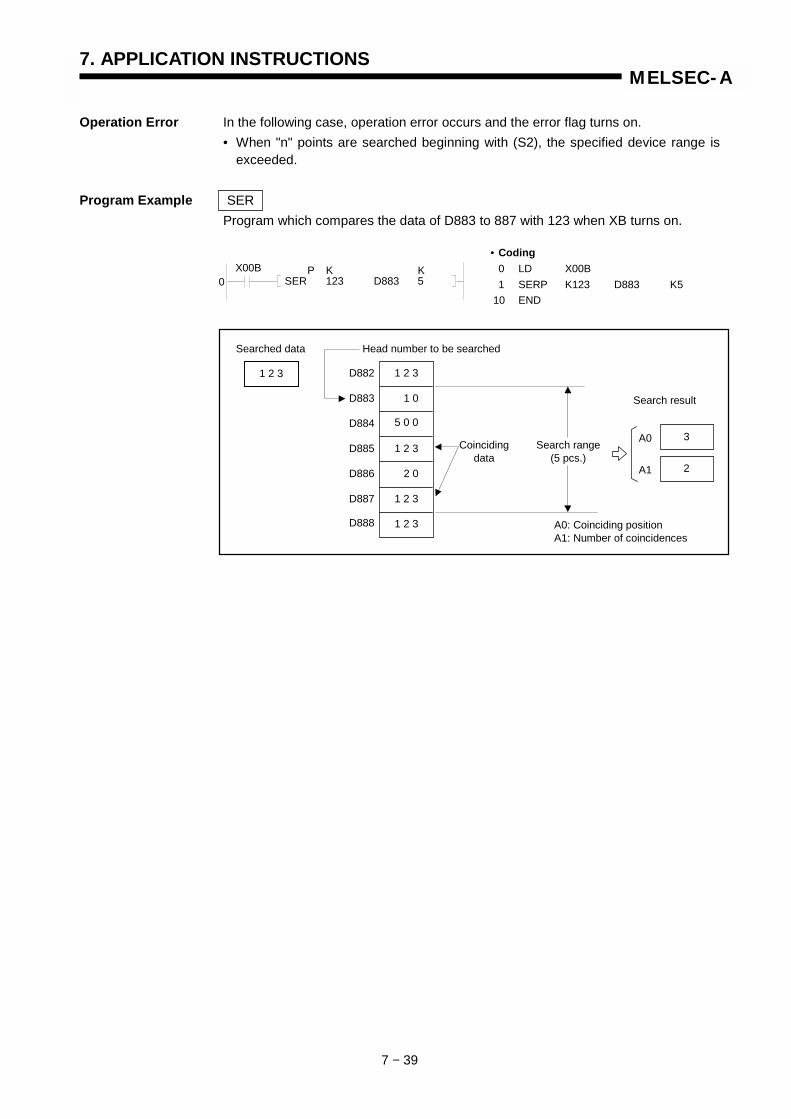
7. APPLICATION INSTRUCTIONS
7 − 39
MELSEC-A
Operation Error In the following case, operation error occurs and the error flag turns on.• When "n" points are searched beginning with (S2), the specified device range is
exceeded.
Program Example SERProgram which compares the data of D883 to 887 with 123 when XB turns on.
X00B0
P K KSER 123 D883 5
• Coding0 LD X00B1 SERP K123 D883 K5
10 END
Searched data
1 2 3
3
Head number to be searched
D882
D883
D884
D885
D886
D887
D888
1 2 3
1 0
5 0 0
1 2 3
2 0
1 2 3
1 2 3
Coincidingdata
Search range(5 pcs.)
2
A0
A1
Search result
A0: Coinciding positionA1: Number of coincidences
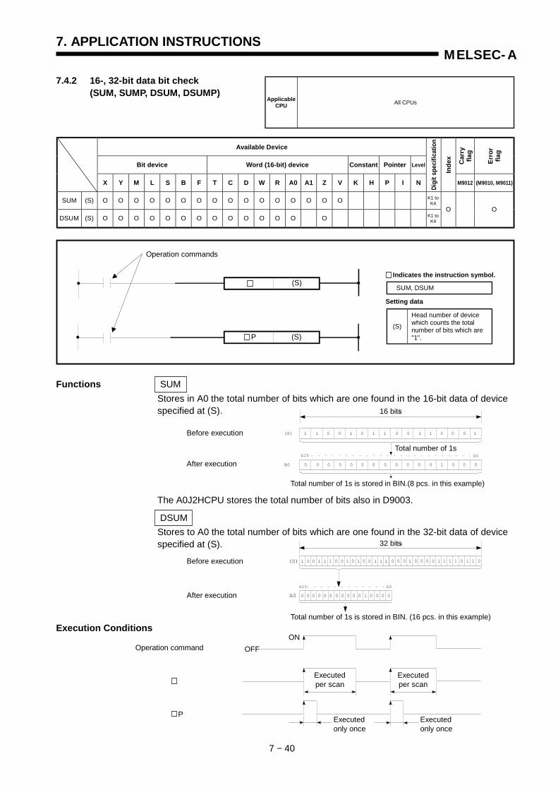
7. APPLICATION INSTRUCTIONS
7 − 40
MELSEC-A
7.4.2 16-, 32-bit data bit check(SUM, SUMP, DSUM, DSUMP)
Available Device
Bit device Word (16-bit) device Constant Pointer Level Car
ryfla
g
Erro
rfla
g
X Y M L S B F T C D W R A0 A1 Z V K H P I N
Digi
t spe
cific
atio
n
Inde
x
M9012 (M9010, M9011)
SUM (S) O O O O O O O O O O O O O O O O
DSUM (S) O O O O O O O O O O O O O OO O
Functions SUMStores in A0 the total number of bits which are one found in the 16-bit data of devicespecified at (S).
The A0J2HCPU stores the total number of bits also in D9003.
DSUMStores to A0 the total number of bits which are one found in the 32-bit data of devicespecified at (S).
Execution Conditions
ApplicableCPU All CPUs
K1 toK4
K1 toK4
Operation commands
(S)
Head number of devicewhich counts the totalnumber of bits which are"1".
Setting data
SUM, DSUM
Indicates the instruction symbol.(S)
(S)P
OFFON
Executedper scan
Executedper scan
Executedonly once
Executedonly once
Operation command
P
1 1 0 0 10 1 1 0 0 1 01 0 10(S)
A0 0 0 0 0 00 0 0 0 0 0 00 1 00
16 bits
b15 b0
Before execution
After execution
Total number of 1s
Total number of 1s is stored in BIN.(8 pcs. in this example)
16 bits
Before execution
After execution
Total number of 1s is stored in BIN. (16 pcs. in this example)
1 00 01 0 01 1 1 01 10 11 00 0 1 0 00 0 1 11 01 1 01(S)
32 bits
0 000 00000 1 000000
b15 b0
A0
32 bits
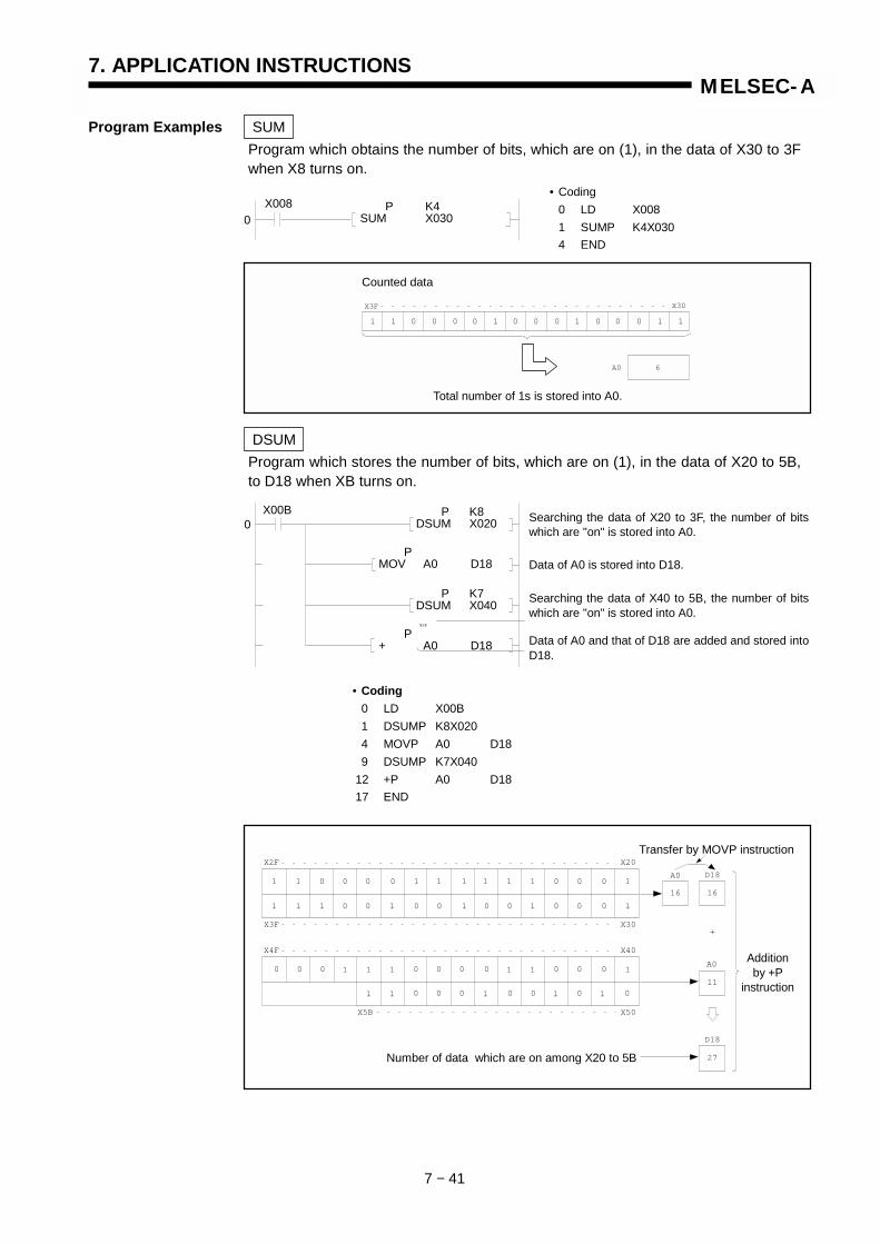
7. APPLICATION INSTRUCTIONS
7 − 41
MELSEC-A
Program Examples SUMProgram which obtains the number of bits, which are on (1), in the data of X30 to 3Fwhen X8 turns on.
DSUMProgram which stores the number of bits, which are on (1), in the data of X20 to 5B,to D18 when XB turns on.
• Coding0 LD X0081 SUMP K4X0304 END
X0080
P K4SUM X030
1 1 0 0 0 0 1 0 0 0 1 0 0 0 1 1
X3F X30
6A0
Counted data
Total number of 1s is stored into A0.
Searching the data of X20 to 3F, the number of bitswhich are "on" is stored into A0.
X3F
X00B0
P K8DSUM X020
P K7DSUM X040
PMOV A0 D18
P+ A0 D18
Data of A0 is stored into D18.
Searching the data of X40 to 5B, the number of bitswhich are "on" is stored into A0.
Data of A0 and that of D18 are added and stored intoD18.
• Coding0 LD X00B1 DSUMP K8X0204 MOVP A0 D189 DSUMP K7X040
12 +P A0 D1817 END
X2F X20
X3F X30
X4F X40
X50X5B
1 1 1 1 1 1 1 1 1
1 1 1 1 1 1 1
11 11 11
1 1 1 1 1
0 0 0 0
0 0 0 0 0 0
0 0 0
0 0 0
0 0 00 0 000 00
0 00 0 0 0 0
16
A0
16
D18
11
A0
+
27
D18
Transfer by MOVP instruction
Additionby +P
instruction
Number of data which are on among X20 to 5B

7. APPLICATION INSTRUCTIONS
7 − 42
MELSEC-A
7.4.3 8 ↔↔↔↔ 256-bit decode, encode(DECO, DECOP, ENCO, ENCOP)
Available Device
Bit device Word (16-bit) device Constant Pointer Level Car
ryfla
g
Erro
rfla
g
X Y M L S B F T C D W R A0 A1 Z V K H P I N
Digi
t spe
cific
atio
n
Inde
x
M9012 (M9010, M9011)
(S) O O O O O O O O O O O O O O O O O O
(D) O O O O O O O O O O ODECO
n O O
(S) O O O O O O O O O O O O O O O O
(D) O O O O O O O O OENCO
n O O
O O
Functions DECO8 → 256 bit decode(1) Decodes the lower "n" bits of device specified at (S) and stores the result of
decode data to 2n bits which begin with the device specified at (D).(2) For "n", 1 to 8 can be specified.(3) When "n" is 0, no processing is performed and the contents of 2n bits, which
begin with the device specified at (D), do not change.(4) A bit device is treated as one bit and a word device as 16 bits.
ENCO256 → 8 bit decode(1) Encodes the data of 2n bits, which begin with (S), and stores the result to (D).(2) For "n", 0 to 8 can be specified.(3) When "n" is 0, no processing is performed and the contents of (D) do not
change.(4) The bit device is treated as one bit and the word device as 16 bits.(5) When multiple bits are 1, processing is performed for the last bit position.
ApplicableCPU All CPUs
(S)Decode, encode data orhead device number stor-ing decode, encode data
(D)Head device numberwhich will store the op-eration result
n Effective bit length (1 to 8)
Setting data
DECO, ENCO
Indicates the instruction symbol.
P
(S) (D) n
(S) (D) n
Decode, encode commands

7. APPLICATION INSTRUCTIONS
7 − 43
MELSEC-A
Execution Conditions
Operation Errors In the following case, operation error occurs and the error flag turns on.• "n" in other than 0 to 8.• 0 exists in all devices from S to 2n when the encode instruction is used.
Program Examples DECO
ENCO
OFFON
Executedper scan
Executedper scan
Executedonly once
Executedonly once
Decode Encode command
P
M00
P KDECO X000 M10 3
• Coding0 LD M01 DECOP X000 M10 K3
10 END
0 0 0 0 0 0 0 0 0 0 0 1 0 0 0
M265 M10M17
0 0 1 1
X2 X1 X0
When 3 is specified atX0 to 2
When 8 is specified at effective bits,256 points are occupied.
Decode result
When 3 is specified as effective bits,8 points are occupied.
Data
M13 at the third position from M10 turns on.
X00C0
P KENCO M10 D8 3
CIRCUIT END
• Coding0 LD X00C1 ENCOP M10 D8 K3
10 END
0 0 0 0 0 0 0 0 0 0 0 1 0 0 0
M265 M10M17
0 0 0 0 0 0 0 0 0 0 0 0 0 0 1 1
When 8 is specified as effective bits,256 points are occupied.
When 3 is specified as effective bits,8 points are occupied.
Device D8Encode result
Which point, counting from M10, is on is stored in BIN.
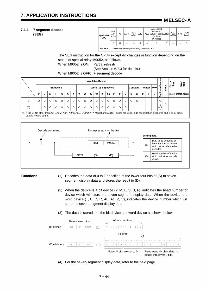
7. APPLICATION INSTRUCTIONS
7 − 44
MELSEC-A
7.4.4 7 segment decode(SEG)
The SEG instruction for the CPUs except An changes in function depending on thestatus of special relay M9052, as follows.When M9052 is ON: Partial refresh
(See Section 6.7.3 for details.)When M9052 is OFF: 7-segment decode
Available Device
Bit device Word (16-bit) device Constant Pointer Level Car
ryfla
g
Erro
rfla
g
X Y M L S B F T C D W R A0 A1 Z V K H P I N
Digi
t spe
cific
atio
n
Inde
x
M9012 (M9010, M9011)
(S) O O O O O O O O O O O O O O O O O O K1
(D) O O O O O O O O O O O O O O OO
*1: If the CPUs other than A3H, A3M, AnA, A2AS,AnU, QCPU-A (A Mode) and A2USH board are used, digit specification is ignored and 8-bit (2 digits)data is always output.
Functions (1) Decodes the data of 0 to F specified at the lower four bits of (S) to seven-segment display data and stores the result to (D).
(2) When the device is a bit device (Y, M, L, S, B, F), indicates the head number ofdevice which will store the seven-segment display data. When the device is aword device (T, C, D, R, A0, A1, Z, V), indicates the device number which willstore the seven-segment display data.
(3) The data is stored into the bit device and word device as shown below.
(4) For the seven-segment display data, refer to the next page.
AnSAnN
AnSHAn A1FX A3H
A3M A3V AnA
AnU, A2ASA2USH-S1
A2USH boardQCPU-A(A Mode)
A0J2H A2CA52G A73 A3N
boadApplicableCPU
O X
Remark * Valid only when special relay M9052 is OFF.
* * * * * * * * *
K1to *1K4
Decode command Not necessary for the An.
(S) (D)
M9052RST
SEG
(S)
Data to be decoded orhead number of devicewhich stores data to bedecoded
(D)Head number of devicewhich will store decoderesult.
Setting data
Before execution
Bit device
After execution
Word device
8 points
Upper 8 bits are set to 0. 7-segment display data isstored into lower 8 bits.
0 0 0 0 0 0 0 0 0 0 1 0 0 1 1 1
0 0 1
Y4F
0 0 1 1 1
Y48
b15 b0
D8
SEG K7
SEG K7
K2Y48
D8
D8
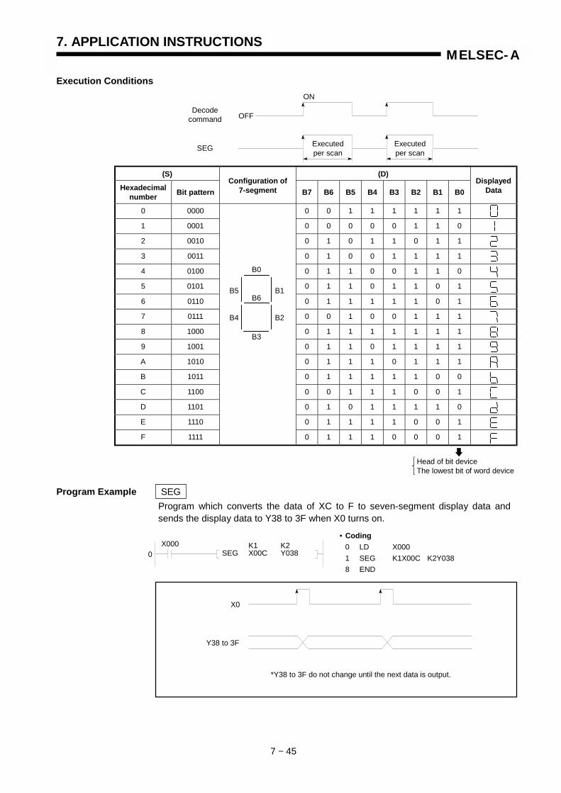
7. APPLICATION INSTRUCTIONS
7 − 45
MELSEC-A
Execution Conditions
(S) (D)
Hexadecimalnumber Bit pattern
Configuration of7-segment B7 B6 B5 B4 B3 B2 B1 B0
DisplayedData
0 0000 0 0 1 1 1 1 1 1
1 0001 0 0 0 0 0 1 1 0
2 0010 0 1 0 1 1 0 1 1
3 0011 0 1 0 0 1 1 1 1
4 0100 0 1 1 0 0 1 1 0
5 0101 0 1 1 0 1 1 0 1
6 0110 0 1 1 1 1 1 0 1
7 0111 0 0 1 0 0 1 1 1
8 1000 0 1 1 1 1 1 1 1
9 1001 0 1 1 0 1 1 1 1
A 1010 0 1 1 1 0 1 1 1
B 1011 0 1 1 1 1 1 0 0
C 1100 0 0 1 1 1 0 0 1
D 1101 0 1 0 1 1 1 1 0
E 1110 0 1 1 1 1 0 0 1
F 1111 0 1 1 1 0 0 0 1
Program Example SEGProgram which converts the data of XC to F to seven-segment display data andsends the display data to Y38 to 3F when X0 turns on.
X0
Y38 to 3F
*Y38 to 3F do not change until the next data is output.
OFF
ON
Executedper scan
Executedper scan
Decodecommand
SEG
B0
B6
B3
B5 B1
B4 B2
Head of bit deviceThe lowest bit of word device
• Coding0 LD X0001 SEG K1X00C K2Y0388 END
X0000
K1 K2SEG X00C Y038

7. APPLICATION INSTRUCTIONS
7 − 46
MELSEC-A
7.4.5 Word device bit set, reset(BSET, BSETP, BRST, BRSTP)
Available Device
Bit device Word (16-bit) device Constant Pointer Level Car
ryfla
g
Erro
rfla
g
X Y M L S B F T C D W R A0 A1 Z V K H P I N
Digi
t spe
cific
atio
n
Inde
x
M9012 (M9010, M9011)
(D) O O O O O O O O O
n O OO O
Functions BSET(1) Sets (1) the "n"th bit of word device specified at (D).
(2) For "n", 0 to 15 are effective. When 15 is exceeded, the instruction is executedat the lower four bits.
BRST(1) Resets (0) the "n"th bit of word device specified at (D).
(2) For "n", 0 to 15 are effective. When 15 is exceeded, the instruction is executedat the lower four bits.
ApplicableCPU All CPUs
(D) Device number for bit set,reset
n Bit number for bit set,reset
Setting data
BSET, BRST
Indicates the instruction symbol.
Set/reset commands
P
(D) n
(D) n
b15 b0b14 b6 b1
D10 1 1 0 0 10 1 1 0 0 1 01 1 11
D10 1 1 0 0 10 1 1 0 1 1 01 1 11
Before execution
After execution
Set to 1.
P KBSET D10 6
P KBRST D10 11
Before execution
After execution
Set to 0.
b15 b0b14 b1
D10 1 1 0 0 10 1 1 0 0 1 01 1 11
D10 1 1 0 0 10 0 1 0 0 1 01 1 11
b11

7. APPLICATION INSTRUCTIONS
7 − 47
MELSEC-A
Execution Conditions
Program Example BEST , BRSTProgram which sets the 3rd bit and 8th bit of D19 when X18 turns on.
OFFON
Executedper scan
Executedper scan
Executedonly once
Executedonly once
Set Reset command
P
• Coding0 LDI X00B1 BRSTP D8 K88 LD X00B9 BSETP D8 K3
16 END
D8 0 0 1 1 01 0 1 1 1 1 01 0 10
0 1 0 0 10 1 1 1 0 0 10 1 10
b0b15 b8 b3
D8
b0b15 b8 b3
Before execution
After execution
When XB turns off When XBturns on
The 8th bit of D8 is reset.
The 3rd bit of D8 is set.
X00B
X00B
0
8
P KBRST D8 8
P KBSET D8 3
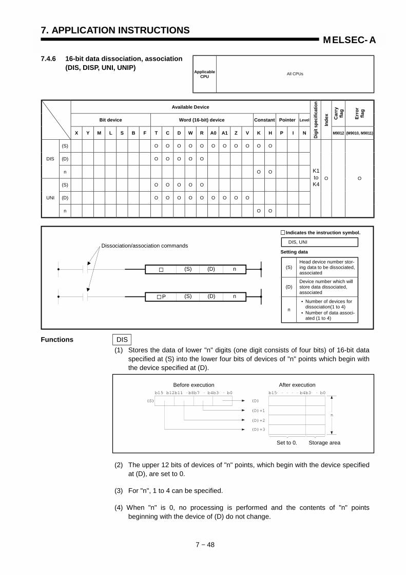
7. APPLICATION INSTRUCTIONS
7 − 48
MELSEC-A
7.4.6 16-bit data dissociation, association(DIS, DISP, UNI, UNIP)
Available Device
Bit device Word (16-bit) device Constant Pointer Level Car
ryfla
g
Erro
rfla
g
X Y M L S B F T C D W R A0 A1 Z V K H P I N
Digi
t spe
cific
atio
n
Inde
x
M9012 (M9010, M9011)
(S) O O O O O O O O O O O
(D) O O O O ODIS
n O O
(S) O O O O O
(D) O O O O O O O O OUNI
n O O
O O
Functions DIS(1) Stores the data of lower "n" digits (one digit consists of four bits) of 16-bit data
specified at (S) into the lower four bits of devices of "n" points which begin withthe device specified at (D).
(2) The upper 12 bits of devices of "n" points, which begin with the device specifiedat (D), are set to 0.
(3) For "n", 1 to 4 can be specified.
(4) When "n" is 0, no processing is performed and the contents of "n" pointsbeginning with the device of (D) do not change.
(S)Head device number stor-ing data to be dissociated,associated
(D)Device number which willstore data dissociated,associated
n• Number of devices for
dissociation(1 to 4)• Number of data associ-
ated (1 to 4)
Setting data
DIS, UNI
Indicates the instruction symbol.
ApplicableCPU All CPUs
K1toK4
Dissociation/association commands
P
(D) n
(D) n
(S)
(S)
(D)(S)
b15 b12b11 b8b7 b4b3 b0
(D)+1
(D)+2
(D)+3
b15 b4b3 b0
n
Before execution
Set to 0. Storage area
After execution
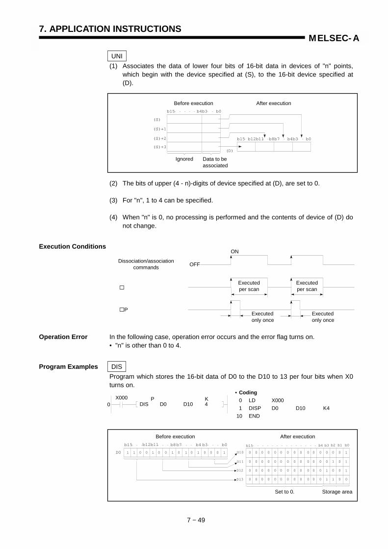
7. APPLICATION INSTRUCTIONS
7 − 49
MELSEC-A
UNI(1) Associates the data of lower four bits of 16-bit data in devices of "n" points,
which begin with the device specified at (S), to the 16-bit device specified at(D).
(2) The bits of upper (4 - n)-digits of device specified at (D), are set to 0.
(3) For "n", 1 to 4 can be specified.
(4) When "n" is 0, no processing is performed and the contents of device of (D) donot change.
Execution Conditions
Operation Error In the following case, operation error occurs and the error flag turns on.• "n" is other than 0 to 4.
Program Examples DISProgram which stores the 16-bit data of D0 to the D10 to 13 per four bits when X0turns on.
OFF
ON
Executedper scan
Executedper scan
Executedonly once
Executedonly once
Dissociation/associationcommands
P
X0000
P KDIS D0 D10 4
• Coding0 LD X0001 DISP D0 D10 K4
10 END
1 1 0 0 00 1 1 0 1 0 01 0 10
b15 b12b11
D11
D10
D12
b8b7 b4 b3 b0
D0
b15 b4 b3 b0b1b2
0 0 0 0 00 0 0 0 0 0 0 0 10
0 0 0 0 00 0 0 0 0 0 10 0 0
0 0 0 0 00 0 0 0 0 0 0 0
0 0 0 0 00 0 0 0 0 0 10 00
1
1
0
0
1
1
D13
Before execution After execution
Set to 0. Storage area
(D)
(S)
(S)+1
(S)+2
(S)+3
b15 b4b3 b0
b15 b12b11 b8b7 b4b3 b0
Before execution After execution
Ignored Data to beassociated
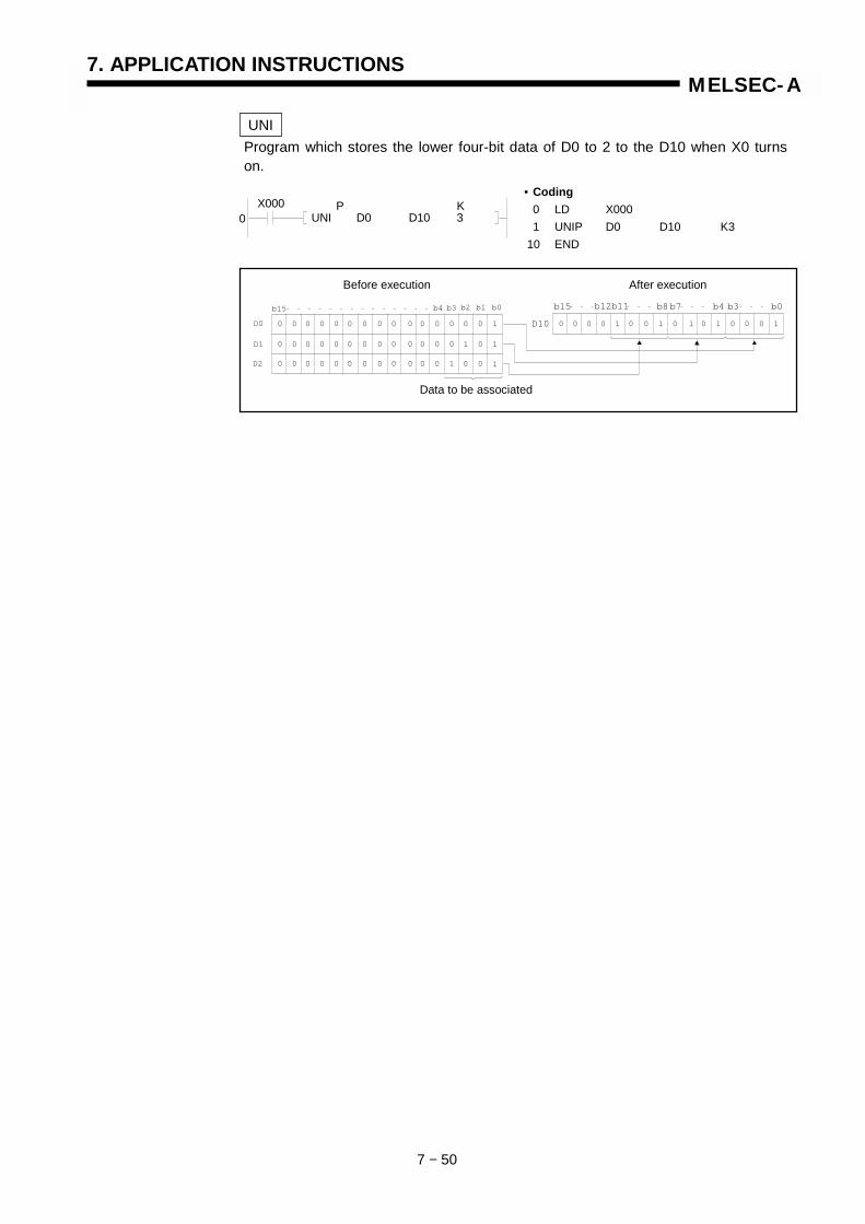
7. APPLICATION INSTRUCTIONS
7 − 50
MELSEC-A
UNIProgram which stores the lower four-bit data of D0 to 2 to the D10 when X0 turnson.
X0000
P KUNI D0 D10 3
• Coding0 LD X0001 UNIP D0 D10 K3
10 END
D1
D0
D2
b15 b4 b3 b0b1b2
0 0 0 0 00 0 0 0 0 0 0 0 10
0 0 0 0 00 0 0 0 0 0 10 0 0
0 0 0 0 00 0 0 0 0 0 0 0
1
1
0
01
0 0 00 1 1 0 1 0 01 0 10
b15 b12b11 b8b7 b4 b3 b0
D10 0 0
Before execution After execution
Data to be associated

MEMO

7. APPLICATION INSTRUCTIONS
7 − 51
MELSEC-A
7.4.7 ASCII code conversion(ASC)
Available Device
Bit device Word (16-bit) device Constant Pointer Level Car
ryfla
g
Erro
rfla
g
X Y M L S B F T C D W R A0 A1 Z V K H P I N
Digi
t spe
cific
atio
n
Inde
x
M9012 (M9010, M9011)
(D) O O O O O O O
Function Converts the specified alphanumeric characters into the ASCII code and stores the result into devices of four points which begin with the device specified at (D).
Executed Conditions
ASC
D10
D11
D12
ABCDEFGH D9
D9 42(B) 41(A)
43(C)
45(E)
47(G)
44(D)
46(F)
48(H)
ApplicableCPU All CPUs
(D)Head number of devicewhich will store ASCIIcode
Setting data
Conversion command
(D)ASC ASCII characters(8 characters)
Before execution
Conversion into ASCII code
After execution
Lower8 bits
Upper8 bits
ASCII code to be stored (hexadecimal)
OFF
ON
Conversion command
ASCExecutedonly once
Executedonly once

7. APPLICATION INSTRUCTIONS
7 − 52
MELSEC-A
Program Example ASCProgram which converts "ABCDEFGHIJKLMNOP" into the ASCII code and storesthe result to the D88 to 95 when X8 turns on, and displays the ASCII data of D88 to95 at the LED indicator on the front face of CPU when X16 turns on.
X0080 ASC ABCDEFGH D88
ASC IJKLMNOP D92
Eight characters, A to H, are converted into ASCIIcode and stored into the D88 to 91.
Eight characters, I to P, are converted into ASCIIcode and stored into the D92 to 95.
• Coding0 LD X0081 ASC ABCDEFGH D88
14 ASC IJKLMNOP D9227 END

7. APPLICATION INSTRUCTIONS
7 − 53
MELSEC-A
7.5 FIFO Instructions
The FIFO instructions perform the write and read of data to and from the FIFO table.
Classification Instruction Symbol Ref. Page
FIFW 7-54Write
FIFWP 7-54
FIFR 7-54Read
FIFRP 7-54

MEMO
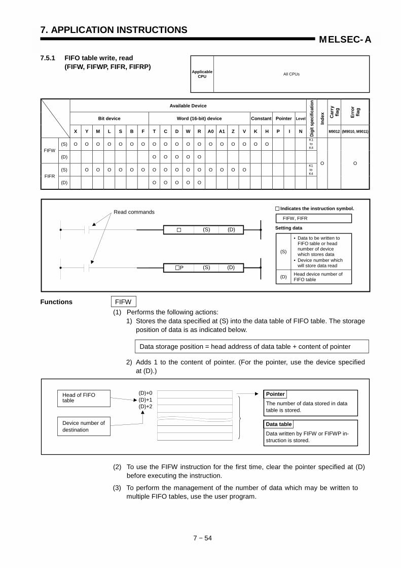
7. APPLICATION INSTRUCTIONS
7 − 54
MELSEC-A
7.5.1 FIFO table write, read(FIFW, FIFWP, FIFR, FIFRP)
Available Device
Bit device Word (16-bit) device Constant Pointer Level Car
ryfla
g
Erro
rfla
g
X Y M L S B F T C D W R A0 A1 Z V K H P I N
Digi
t spe
cific
atio
n
Inde
x
M9012 (M9010, M9011)
(S) O O O O O O O O O O O O O O O O O OFIFW
(D) O O O O O
(S) O O O O O O O O O O O O O O OFIFR
(D) O O O O O
O O
Functions FIFW(1) Performs the following actions:
1) Stores the data specified at (S) into the data table of FIFO table. The storageposition of data is as indicated below.
Data storage position = head address of data table + content of pointer
2) Adds 1 to the content of pointer. (For the pointer, use the device specifiedat (D).)
(2) To use the FIFW instruction for the first time, clear the pointer specified at (D)before executing the instruction.
ApplicableCPU All CPUs
K1toK4
K1toK4
(3) To perform the management of the number of data which may be written tomultiple FIFO tables, use the user program.
Read commands Indicates the instruction symbol.
(S)
• Data to be written to FIFO table or head number of device which stores data
• Device number which will store data read
(D) Head device number ofFIFO table
Setting data
FIFW, FIFR
(S) (D)
(D)(S)P
PointerThe number of data stored in datatable is stored.
Head of FIFOtable
Device number ofdestination
(D)+0(D)+1(D)+2
Data tableData written by FIFW or FIFWP in-struction is stored.
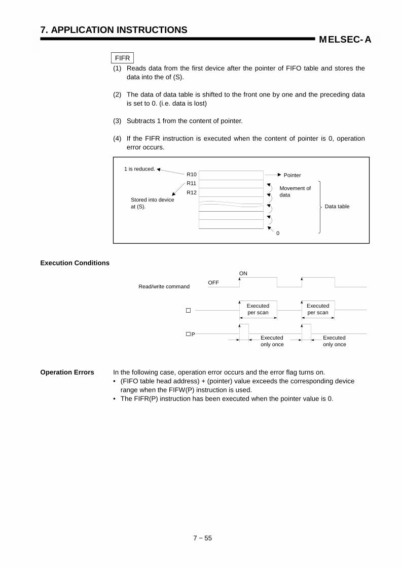
7. APPLICATION INSTRUCTIONS
7 − 55
MELSEC-A
FIFR(1) Reads data from the first device after the pointer of FIFO table and stores the
data into the of (S).
(2) The data of data table is shifted to the front one by one and the preceding datais set to 0. (i.e. data is lost)
(3) Subtracts 1 from the content of pointer.
(4) If the FIFR instruction is executed when the content of pointer is 0, operationerror occurs.
Execution Conditions
Operation Errors In the following case, operation error occurs and the error flag turns on.• (FIFO table head address) + (pointer) value exceeds the corresponding device
range when the FIFW(P) instruction is used.• The FIFR(P) instruction has been executed when the pointer value is 0.
OFFON
Executedper scan
Executedper scan
Executedonly once
Executedonly once
Read/write command
P
Stored into deviceat (S).
1 is reduced.R10R11
R12
0
Data table
Pointer
Movement ofdata

7. APPLICATION INSTRUCTIONS
7 − 56
MELSEC-A
FIFWProgram which uses D38 to 47 as a FIFO table and temporarily stores the data ofX20 to 2F when XB turns on. When the data exceeds 9, this program turns on Y60to disable the execution of FIFW instruction.(The data storage location is as shown below when the pointer value is 5.)
• Coding0 LD> D38 K85 OUT Y0606 LD X00B7 ANI Y0608 FIFWP K4X020 D38
15 END
D45
5
0010
0020
0030
0040
0050
D44
D43
D42
D41
D40
D39
D38
D45
6
0010
0020
0030
0040
0050
8100
8100
D44
D43
D42
D41
D40
D39
D38
X20 to 2F8100
D46 D46
D47 D47
X20 to 2F
PointerBefore execution After execution
Data of X20 to 2F is stored intoFIFO table.
When pointer (D38) is 9 or more,Y60 is turned on.
( )0
6
K> D38 8 Y060
X00B Y060 P K4FIFW X020 D38

7. APPLICATION INSTRUCTIONS
7 − 57
MELSEC-A
FIFRProgram which reads data from D38 to 45 of the FIFO table when XB turns on, andoutputs the data to the Y30 to 3F.(Data is read as shown below when the pointer value is 7.)
• Coding0 LD= K0 D385 OUT Y0606 LD X00B7 ANI Y0608 FIFRP K4Y030 D38
15 END
D45
7
0123
4567
0054
9999
0547
0098
Before execution
1010
D44
D43
D42
D41
D40
D39
D38
Pointer
D45
6
4567
0054
9999
0547
0098
1010
After execution
0123
0000
D44
D43
D42
D41
D40
D39
D38
Y30 to 3FPointer
Before execution After execution
K= 0 D38 Y060 When pointer (D38) is 0, Y60 is
turns on.
Data is read from FIFO table andoutput to Y30 to 3F.
( )0
6P K4
FIFR Y030 D38X00B Y060

7. APPLICATION INSTRUCTIONS
7 − 58
MELSEC-A
7.6 Buffer Memory Access Instructions
Buffer memory access instructions are used to read and write data of buffer memoryof special function modules and remote terminal modules (when the A2C, A52G isused).There are 16 types of buffer memory access instructions as shown below.
Classification Instruction Symbol Ref. Page
FROM 7-59
FROMP 7-59
DFRO 7-59Special function
module data read
DFROP 7-59
TO 7-61
TOP 7-61
DTO 7-61Special function
module data write
DTOP 7-61
FROM, PRC 7-63
FROMP, PRC 7-63
DFRO, PRC 7-63Remote terminal
data read
DFROP, PRC 7-63
TO, PRC 7-67
TOP, PRC 7-67
DTO, PRC 7-67Remote terminal
data write
DTOP, PRC 7-67

MEMO

7. APPLICATION INSTRUCTIONS
7 − 59
MELSEC-A
7.6.1 Special function module 1-, 2-worddata read (FROM, FROMP, DFRO,DFROP)
Available Device
Bit device Word (16-bit) device Constant Pointer Level Car
ryfla
g
Erro
rfla
g
X Y M L S B F T C D W R A0 A1 Z V K H P I N
Dig
it sp
ecifi
catio
n*2
Inde
x
M9012 (M9010, M9011)
n1 O O
n2 O O
(D) O*1 O*1 O*1 O*1 O*1 O*1 O*1 O O O O O
n3 O O
O O
*1: Bit devices cannot be used with the An and A3H CPUs.*2: K1 to K4 when the FROM(P) instruction is used. K1 to K8 when the DFRO(P) instruction is used.
Functions FROMReads the data of "n3" words, which start at the address specified at "n2" of buffermemory inside the special function module specified at "n1", and stores the data intodevices which begin with the device specified at (D).
DFROReads the data of "n3×2" words, which start at the address specified at "n2" ofbuffer memory inside the special function module specified at "n1", and stores thedata into devices which begin with the device specified at (D).
AnSAnN
AnSHAn A1FX A3H
A3M A3V AnA
AnU, A2ASA2USH-S1
A2USH boardQCPU-A(A Mode)
A0J2H A2CA52G A73 A3N
boardApplicableCPU
O O O O O O O O X O O
Remark
Special function modulebuffer memory CPU module
n2
Device specified at (D)
n3 pointsn3 words
Special function modulebuffer memory CPU module
n2
Device specified at (D)
(n3×2)points
(n3×2)words
K1toK4
K1to
K8
n3
n3
n1
Head I/O number of special functionmodule
n2 Head address of data to be read
(D) Device number which will store readdata
n3 Number of data to be read
Setting data
FROM, DFRO
Indicates the instruction symbol.
n1 (D)
n1 (D)P
n2
n2
Read commands
Specified with the upper two digitswhen the head I/O number isexpressed in 3 hexadecimal digits.

7. APPLICATION INSTRUCTIONS
7 − 60
MELSEC-A
REMARK
• Specify n1 with the upper two digits when the head I/O number of the slot in which a special function module is inserted is expressed in 3 hexadecimal digits.
Example
Execution Conditions
Operation Errors In the following cases, operation error occurs and the error flag turns on.• Access cannot be made to the special function module.• The I/O number specified at "n1" is not a special function module.• "n3" points, which begin with the device specified at (D), exceeds the specified
device range.
Program Examples FROMProgram which reads the data of one word from the address 10 of buffer memory ofA68AD, loaded in I/O numbers 040 to 05F to D0.
DFROProgram which reads the data of two words from the address 10 of buffer memory ofA68AD, loaded in I/O numbers 040 to 05F to D0 and 1.
POINT
If a FROM instruction is executed for a special function module frequently in ashort scan time, the objective special function module may fail to processcorrectly.To execute a FROM instruction for a special function module, set the execu-tion intervals meeting the processing and conversion time of that moduleusing the timer and the constant scan function of it.
X000
X00F
X010
X01F
X020
X02F
X030
X03F
040
05F
060
07F
Y080
Y08F
Y090
Y09F
to to to to to to to to
Head I/O number to be read, K4 or H4
Pow
er s
uppl
ym
odul
e
CPU
mod
ule
AX10
AX10
AX10
AX10
A68A
D
AD71
AY10
AY10
OFFON
Executedper scan
Executedper scan
Executedonly once
Executedonly once
P
Read command
X0000
H K KFROM 0004 10 D0 1
•••• Coding0 LD X0001 FROM H0004 K10 D0 K1
10 END
X0000
H K KDFRO 0004 10 D0 1
•••• Coding0 LD X0001 DFRO H0004 K10 D0 K1
10 END
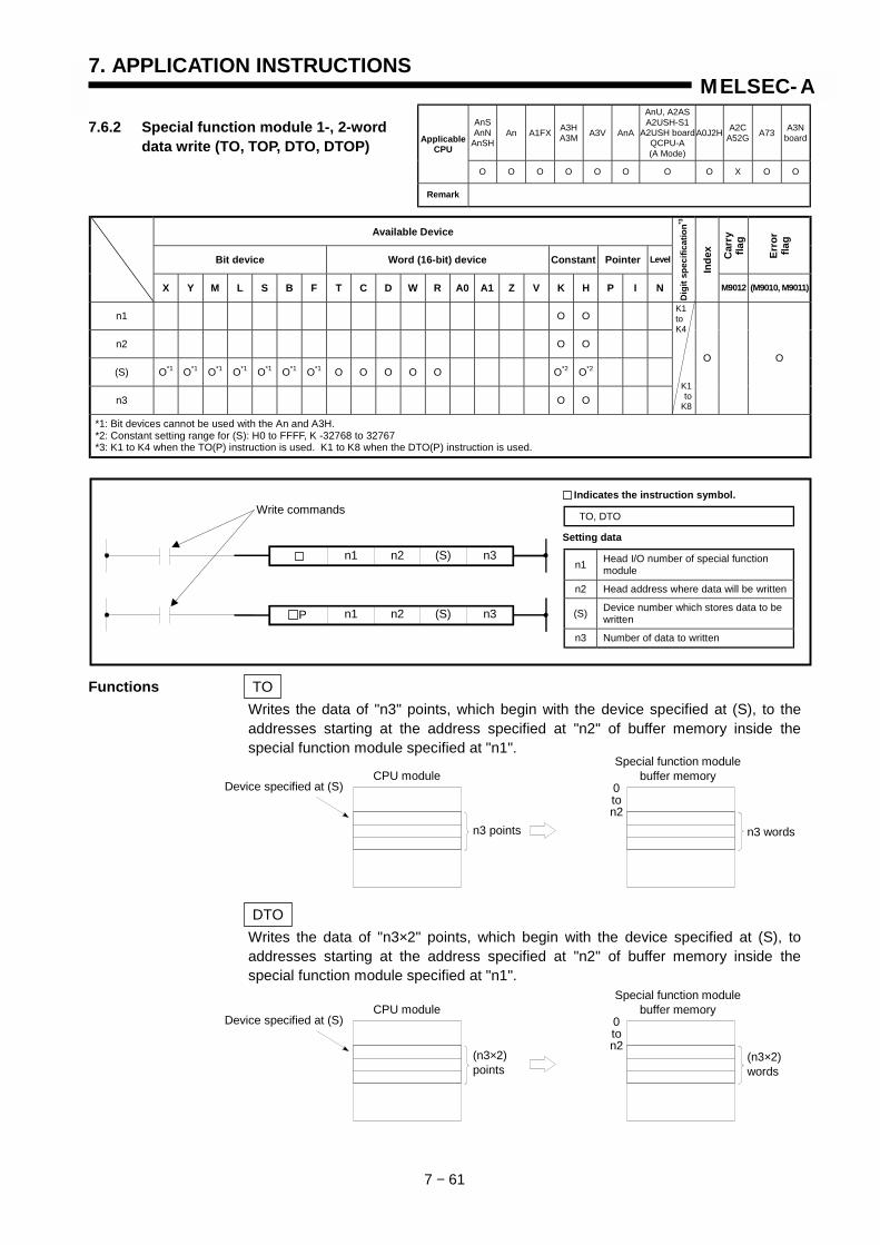
7. APPLICATION INSTRUCTIONS
7 − 61
MELSEC-A
7.6.2 Special function module 1-, 2-worddata write (TO, TOP, DTO, DTOP)
Available Device
Bit device Word (16-bit) device Constant Pointer Level Car
ryfla
g
Erro
rfla
g
X Y M L S B F T C D W R A0 A1 Z V K H P I N
Dig
it sp
ecifi
catio
n*3
Inde
x
M9012 (M9010, M9011)
n1 O O
n2 O O
(S) O*1 O*1 O*1 O*1 O*1 O*1 O*1 O O O O O O*2 O*2
n3 O O
O O
*1: Bit devices cannot be used with the An and A3H.*2: Constant setting range for (S): H0 to FFFF, K -32768 to 32767*3: K1 to K4 when the TO(P) instruction is used. K1 to K8 when the DTO(P) instruction is used.
Functions TOWrites the data of "n3" points, which begin with the device specified at (S), to theaddresses starting at the address specified at "n2" of buffer memory inside thespecial function module specified at "n1".
DTOWrites the data of "n3×2" points, which begin with the device specified at (S), toaddresses starting at the address specified at "n2" of buffer memory inside thespecial function module specified at "n1".
AnSAnN
AnSHAn A1FX A3H
A3M A3V AnA
AnU, A2ASA2USH-S1
A2USH boardQCPU-A(A Mode)
A0J2H A2CA52G A73 A3N
boardApplicableCPU
O O O O O O O O X O O
Remark
K1toK4
K1to
K8
Special function modulebuffer memoryCPU module
0ton2
Device specified at (S)
n3 points n3 words
Special function modulebuffer memoryCPU module
0ton2
Device specified at (S)
(n3×2)points
(n3×2)words
n3
n3
n1 Head I/O number of special functionmodule
n2 Head address where data will be written
(S) Device number which stores data to bewritten
n3 Number of data to written
Setting data
TO, DTO
Indicates the instruction symbol.
n1 (S)
n1 (S)P
n2
n2
Write commands
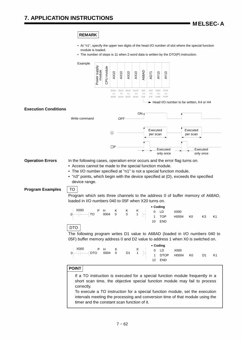
7. APPLICATION INSTRUCTIONS
7 − 62
MELSEC-A
REMARK
• At "n1", specify the upper two digits of the head I/O number of slot where the special function module is loaded.
• The number of steps is 11 when 2-word data is written by the DTO(P) instruction.
Example
Execution Conditions
Operation Errors In the following cases, operation error occurs and the error flag turns on.• Access cannot be made to the special function module.• The I/O number specified at "n1" is not a special function module.• "n3" points, which begin with the device specified at (D), exceeds the specified
device range.
Program Examples TOProgram which sets three channels to the address 0 of buffer memory of A68AD,loaded in I/O numbers 040 to 05F when X20 turns on.
DTOThe following program writes D1 value to A68AD (loaded in I/O numbers 040 to05F) buffer memory address 0 and D2 value to address 1 when X0 is switched on.
POINT
If a TO instruction is executed for a special function module frequently in ashort scan time, the objective special function module may fail to processcorrectly.To execute a TO instruction for a special function module, set the executionintervals meeting the processing and conversion time of that module using thetimer and the constant scan function of it.
X000
X00F
X010
X01F
X020
X02F
X030
X03F
040
05F
060
07F
Y080
Y08F
Y090
Y09F
to to to to to to to to
Head I/O number to be written, K4 or H4Po
wer
sup
ply
mod
ule
CPU
mod
ule
AX10
AX10
AX10
AX10
A68A
D
AD71
AY10
AY10
OFFON
Executedper scan
Executedper scan
Executedonly once
Executedonly once
P
Write command
X0000
P H K K KTO 0004 0 3 1
•••• Coding0 LD X0001 TOP H0004 K0 K3 K1
10 END
X0000
P H K KDTO 0004 0 D1 1
•••• Coding0 LD X0001 DTOP H0004 K0 D1 K1
12 END

7. APPLICATION INSTRUCTIONS
7 − 63
MELSEC-A
7.6.3 Remote terminal module 1- and2-word data read(FROM, PRC, FROMP, PRC,DFRO, PRC, DFROP, PRC)
Available Device
Bit device Word (16-bit) device Constant Pointer Level Car
ryfla
g
Erro
rfla
g
X Y M L S B F T C D W R A0 A1 Z V K H P I N
Dig
it sp
ecifi
catio
n*1
Inde
x
M9012 (M9010, M9011)
n1 O OFROM
n2 O O
(D1) O O O O ODFRO
n3 O O
O O
(D2) O O O OPRC
(D3) O
*1: K1 to K4 when the FROM(P) instruction is used. K1 to K8 when the DFRO(P) instruction is used.
Functions FROM , PRC(1) Reads data of "n3" words which begin with the address specified at "n2" of
buffer memory in the remote terminal module specified at "n1", and stores thedata in the devices starting with the one specified at (D1).
AnSAnN
AnSHAn A1FX A3H
A3M A3V AnA
AnU, A2ASA2USH-S1
A2USH boardQCPU-A(A Mode)
A0J2H A2CA52G A73 A3N
boardApplicableCPU
X X X X X X X X O X X
Remark
K1toK4
K1to
K8
n3
n3
n1
A2C: Head station number of remote terminal module
A52G: (Head station number of remoteterminal module) + (100)
n2 Head address of data to be read
(D1) Head number of the device which storeread data
n3 Number of data to be read
(D2) Number of the device to be turned on atread completion
(D3) Dummy data which has no meaning inprogram processing
Setting data
FROM, DFRO
Indicates the instruction symbol.
n1 (D1)
n1 (D1)P
n2
n2
Read commands
(D3)(D2)PRC
(D3)(D2)PRC
Not required when the AJ35PTF-R2 RS232C interface unit is used. For details,refer to AJ35PTF-R2 RS-232C interface unit user’s manual.
Remote terminalbuffer memory CPU module
n2
Device specified at (D1)
n3 pointsn3 words
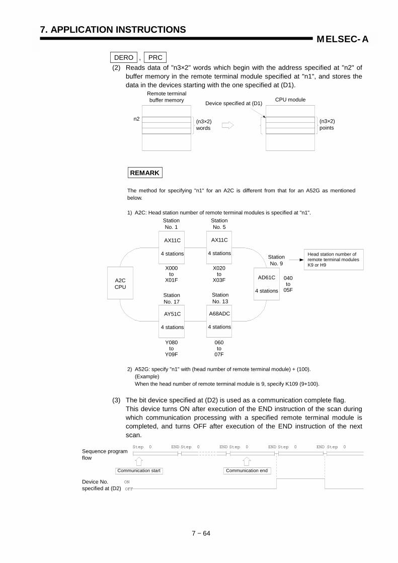
7. APPLICATION INSTRUCTIONS
7 − 64
MELSEC-A
DERO , PRC(2) Reads data of "n3×2" words which begin with the address specified at "n2" of
buffer memory in the remote terminal module specified at "n1", and stores thedata in the devices starting with the one specified at (D1).
REMARK
The method for specifying "n1" for an A2C is different from that for an A52G as mentionedbelow.
1) A2C: Head station number of remote terminal modules is specified at "n1".
2) A52G: specify "n1" with (head number of remote terminal module) + (100).(Example)When the head number of remote terminal module is 9, specify K109 (9+100).
(3) The bit device specified at (D2) is used as a communication complete flag.This device turns ON after execution of the END instruction of the scan duringwhich communication processing with a specified remote terminal module iscompleted, and turns OFF after execution of the END instruction of the nextscan.
Remote terminalbuffer memory CPU module
n2
Device specified at (D1)
(n3×2)points
(n3×2)words
StationNo. 1
StationNo. 5
AX11C
4 stations
AX11C
4 stations
X000to
X01F
X020to
X03F
StationNo. 17
StationNo. 13
A2CCPU
Head station number ofremote terminal modulesK9 or H9
AY51C
4 stations
A68ADC
4 stations
Y080to
Y09F
060to
07F
StationNo. 9
AD61C
4 stations
040to
05F
OFF
ON
Step 0 Step 0 Step 0 Step 0 Step 0ENDENDENDEND
Communication endCommunication start
Sequence programflow
Device No.specified at (D2)
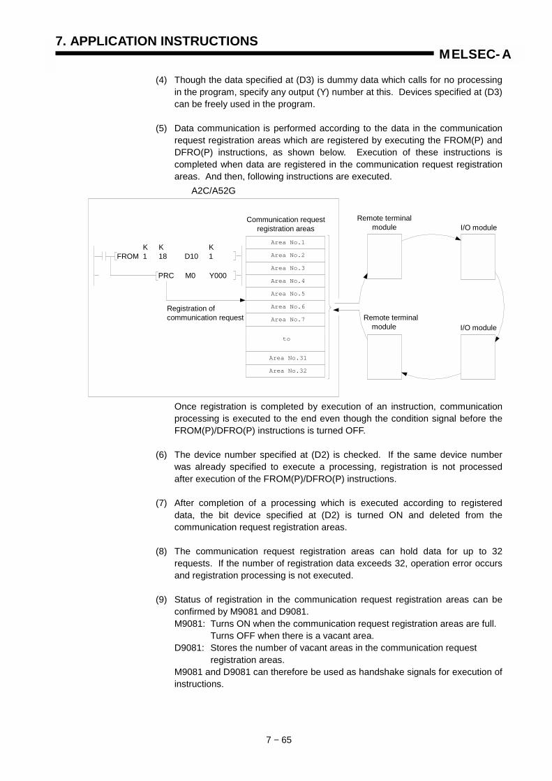
7. APPLICATION INSTRUCTIONS
7 − 65
MELSEC-A
(4) Though the data specified at (D3) is dummy data which calls for no processingin the program, specify any output (Y) number at this. Devices specified at (D3)can be freely used in the program.
(5) Data communication is performed according to the data in the communicationrequest registration areas which are registered by executing the FROM(P) andDFRO(P) instructions, as shown below. Execution of these instructions iscompleted when data are registered in the communication request registrationareas. And then, following instructions are executed.
Once registration is completed by execution of an instruction, communicationprocessing is executed to the end even though the condition signal before theFROM(P)/DFRO(P) instructions is turned OFF.
(6) The device number specified at (D2) is checked. If the same device numberwas already specified to execute a processing, registration is not processedafter execution of the FROM(P)/DFRO(P) instructions.
(7) After completion of a processing which is executed according to registereddata, the bit device specified at (D2) is turned ON and deleted from thecommunication request registration areas.
(8) The communication request registration areas can hold data for up to 32requests. If the number of registration data exceeds 32, operation error occursand registration processing is not executed.
(9) Status of registration in the communication request registration areas can beconfirmed by M9081 and D9081.M9081: Turns ON when the communication request registration areas are full.
Turns OFF when there is a vacant area.D9081: Stores the number of vacant areas in the communication request
registration areas.M9081 and D9081 can therefore be used as handshake signals for execution ofinstructions.
to
Area No.1
Area No.2
Area No.3
Area No.4
Area No.5
Area No.6
Area No.7
Area No.31
Area No.32
A2C/A52G
Remote terminalmodule I/O module
Remote terminal module I/O module
Registration ofcommunication request
Communication requestregistration areas
K K KFROM 1 18 D10 1
PRC M0 Y000
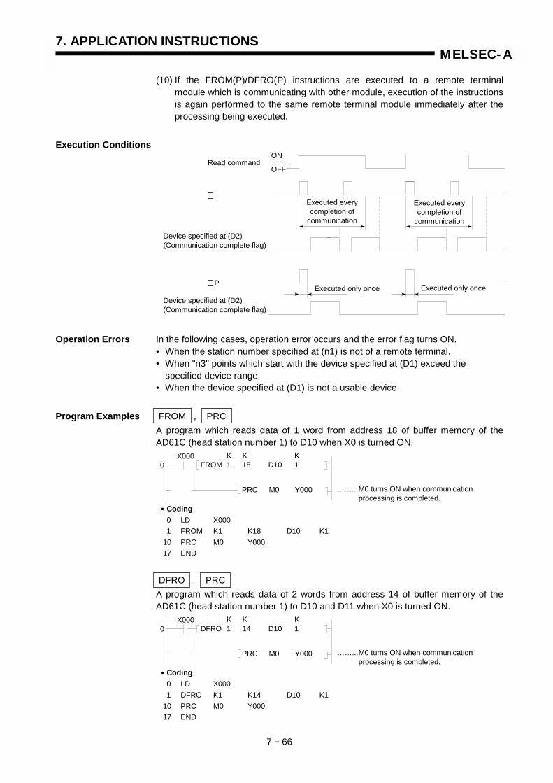
7. APPLICATION INSTRUCTIONS
7 − 66
MELSEC-A
(10) If the FROM(P)/DFRO(P) instructions are executed to a remote terminalmodule which is communicating with other module, execution of the instructionsis again performed to the same remote terminal module immediately after theprocessing being executed.
Execution Conditions
Operation Errors In the following cases, operation error occurs and the error flag turns ON.• When the station number specified at (n1) is not of a remote terminal.• When "n3" points which start with the device specified at (D1) exceed the
specified device range.• When the device specified at (D1) is not a usable device.
Program Examples FROM , PRCA program which reads data of 1 word from address 18 of buffer memory of theAD61C (head station number 1) to D10 when X0 is turned ON.
DFRO , PRCA program which reads data of 2 words from address 14 of buffer memory of theAD61C (head station number 1) to D10 and D11 when X0 is turned ON.
Device specified at (D2)(Communication complete flag)
OFF
ON
Executed everycompletion of
communication
Executed everycompletion of
communication
Executed only once Executed only onceP
Read command
Device specified at (D2)(Communication complete flag)
K K KFROM 1 18 D10 1
PRC M0 Y000
0X000
……...M0 turns ON when communicationprocessing is completed.
•••• Coding0 LD X0001 FROM K1 K18 D10 K1
10 PRC M0 Y00017 END
K K KDFRO 1 14 D10 1
PRC M0 Y000
0X000
……...M0 turns ON when communicationprocessing is completed.
•••• Coding0 LD X0001 DFRO K1 K14 D10 K1
10 PRC M0 Y00017 END
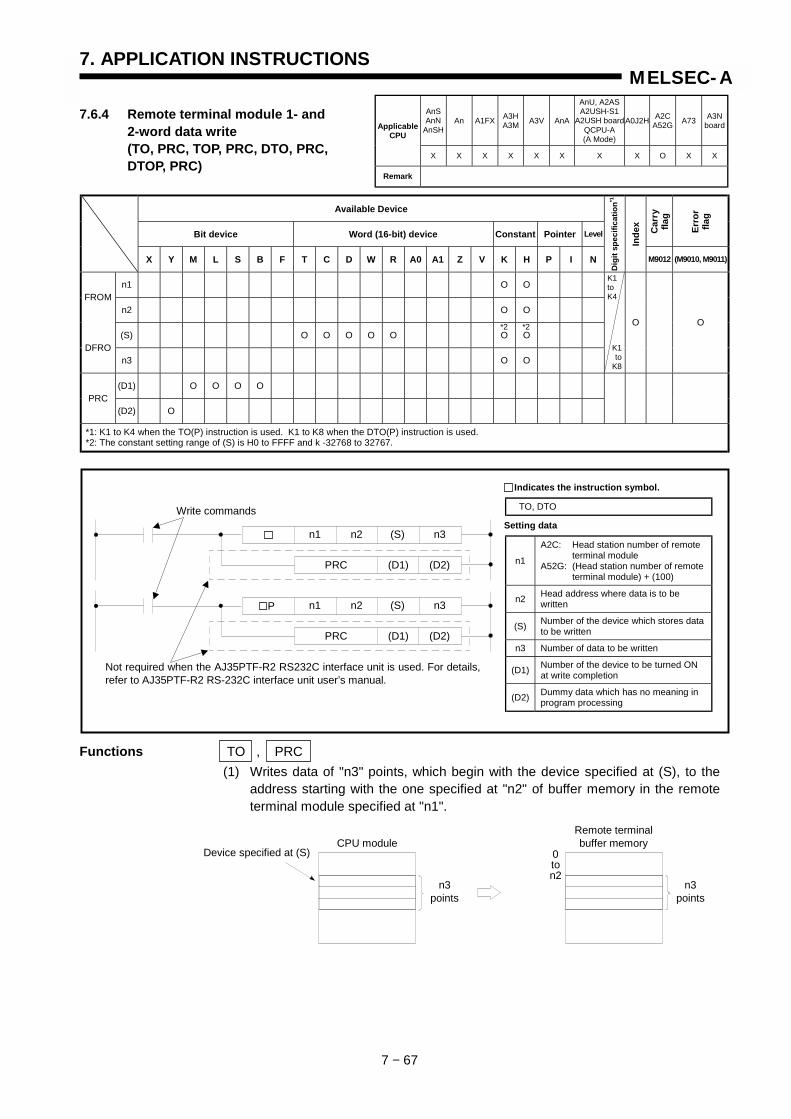
7. APPLICATION INSTRUCTIONS
7 − 67
MELSEC-A
7.6.4 Remote terminal module 1- and2-word data write(TO, PRC, TOP, PRC, DTO, PRC,DTOP, PRC)
Available Device
Bit device Word (16-bit) device Constant Pointer Level Car
ryfla
g
Erro
rfla
g
X Y M L S B F T C D W R A0 A1 Z V K H P I N
Dig
it sp
ecifi
catio
n*1
Inde
x
M9012 (M9010, M9011)
n1 O OFROM
n2 O O
(S) O O O O O O ODFRO
n3 O O
O O
(D1) O O O OPRC
(D2) O
*1: K1 to K4 when the TO(P) instruction is used. K1 to K8 when the DTO(P) instruction is used.*2: The constant setting range of (S) is H0 to FFFF and k -32768 to 32767.
Functions TO , PRC(1) Writes data of "n3" points, which begin with the device specified at (S), to the
address starting with the one specified at "n2" of buffer memory in the remoteterminal module specified at "n1".
AnSAnN
AnSHAn A1FX A3H
A3M A3V AnA
AnU, A2ASA2USH-S1
A2USH boardQCPU-A(A Mode)
A0J2H A2CA52G A73 A3N
boardApplicableCPU
X X X X X X X X O X X
Remark
K1toK4
K1to
K8
*2 *2
n3
n3
n1
A2C: Head station number of remote terminal module
A52G: (Head station number of remoteterminal module) + (100)
n2 Head address where data is to bewritten
(S) Number of the device which stores datato be written
n3 Number of data to be written
(D1) Number of the device to be turned ONat write completion
(D2) Dummy data which has no meaning inprogram processing
Setting data
TO, DTO
Indicates the instruction symbol.
n1 (S)
n1 (S)P
n2
n2
Write commands
(D2)(D1)PRC
(D2)(D1)PRC
Not required when the AJ35PTF-R2 RS232C interface unit is used. For details,refer to AJ35PTF-R2 RS-232C interface unit user’s manual.
Remote terminalbuffer memoryCPU module
0ton2
Device specified at (S)
n3points
n3points
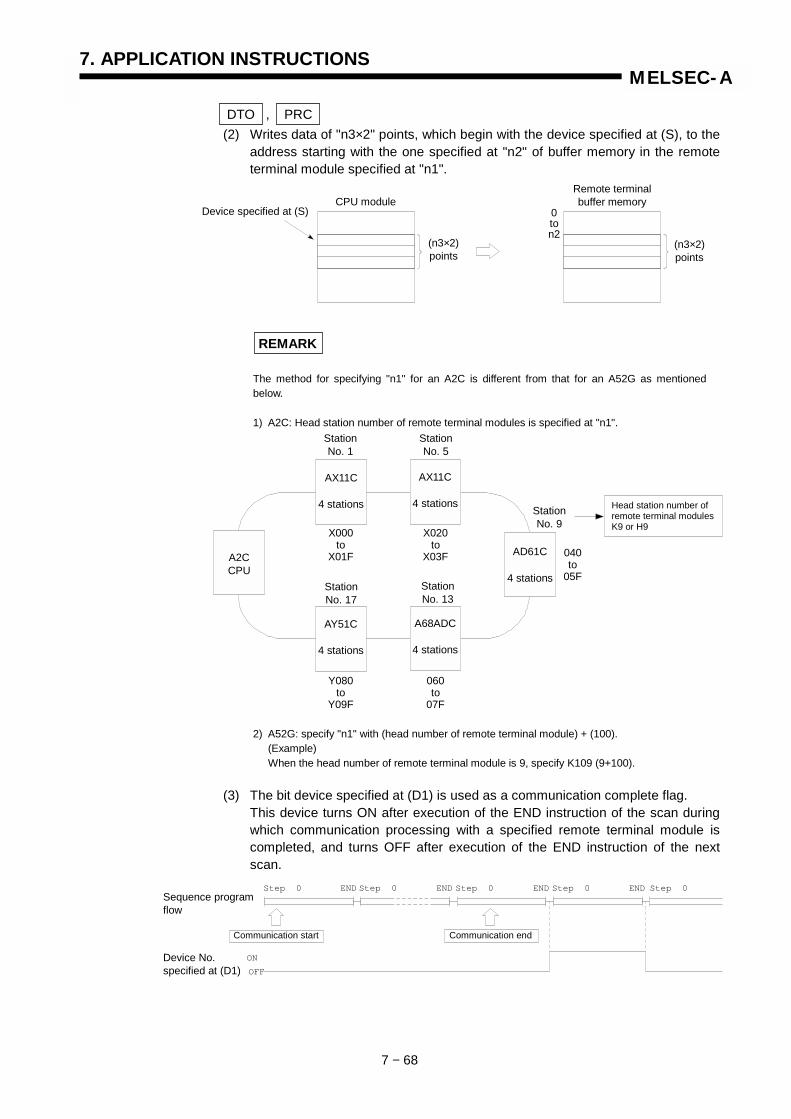
7. APPLICATION INSTRUCTIONS
7 − 68
MELSEC-A
DTO , PRC(2) Writes data of "n3×2" points, which begin with the device specified at (S), to the
address starting with the one specified at "n2" of buffer memory in the remoteterminal module specified at "n1".
REMARK
The method for specifying "n1" for an A2C is different from that for an A52G as mentionedbelow.
1) A2C: Head station number of remote terminal modules is specified at "n1".
2) A52G: specify "n1" with (head number of remote terminal module) + (100).(Example)When the head number of remote terminal module is 9, specify K109 (9+100).
(3) The bit device specified at (D1) is used as a communication complete flag.This device turns ON after execution of the END instruction of the scan duringwhich communication processing with a specified remote terminal module iscompleted, and turns OFF after execution of the END instruction of the nextscan.
Remote terminalbuffer memoryCPU module
0ton2
Device specified at (S)
(n3×2)points
(n3×2)points
StationNo. 1
StationNo. 5
AX11C
4 stations
AX11C
4 stations
X000to
X01F
X020to
X03F
StationNo. 17
StationNo. 13
A2CCPU
Head station number ofremote terminal modulesK9 or H9
AY51C
4 stations
A68ADC
4 stations
Y080to
Y09F
060to
07F
StationNo. 9
AD61C
4 stations
040to
05F
OFF
ON
Step 0 Step 0 Step 0 Step 0 Step 0ENDENDENDEND
Communication endCommunication start
Sequence programflow
Device No.specified at (D1)
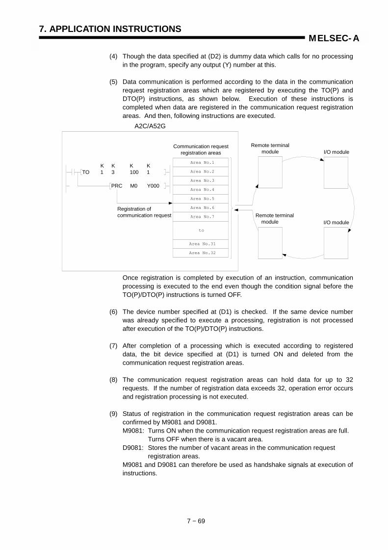
7. APPLICATION INSTRUCTIONS
7 − 69
MELSEC-A
(4) Though the data specified at (D2) is dummy data which calls for no processingin the program, specify any output (Y) number at this.
(5) Data communication is performed according to the data in the communicationrequest registration areas which are registered by executing the TO(P) andDTO(P) instructions, as shown below. Execution of these instructions iscompleted when data are registered in the communication request registrationareas. And then, following instructions are executed.
Once registration is completed by execution of an instruction, communicationprocessing is executed to the end even though the condition signal before theTO(P)/DTO(P) instructions is turned OFF.
(6) The device number specified at (D1) is checked. If the same device numberwas already specified to execute a processing, registration is not processedafter execution of the TO(P)/DTO(P) instructions.
(7) After completion of a processing which is executed according to registereddata, the bit device specified at (D1) is turned ON and deleted from thecommunication request registration areas.
(8) The communication request registration areas can hold data for up to 32requests. If the number of registration data exceeds 32, operation error occursand registration processing is not executed.
(9) Status of registration in the communication request registration areas can beconfirmed by M9081 and D9081.M9081: Turns ON when the communication request registration areas are full.
Turns OFF when there is a vacant area.D9081: Stores the number of vacant areas in the communication request
registration areas.M9081 and D9081 can therefore be used as handshake signals at execution ofinstructions.
to
Area No.1
Area No.2
Area No.3
Area No.4
Area No.5
Area No.6
Area No.7
Area No.31
Area No.32
A2C/A52G
Remote terminalmodule I/O module
Remote terminal module I/O module
Registration ofcommunication request
Communication requestregistration areas
K K K KTO 1 3 100 1
PRC M0 Y000
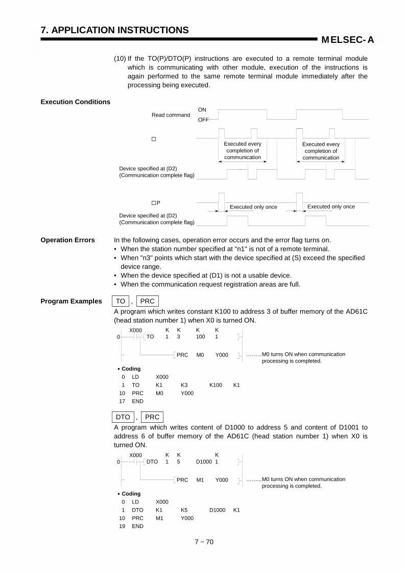
7. APPLICATION INSTRUCTIONS
7 − 70
MELSEC-A
(10) If the TO(P)/DTO(P) instructions are executed to a remote terminal modulewhich is communicating with other module, execution of the instructions isagain performed to the same remote terminal module immediately after theprocessing being executed.
Execution Conditions
Operation Errors In the following cases, operation error occurs and the error flag turns on.• When the station number specified at "n1" is not of a remote terminal.• When "n3" points which start with the device specified at (S) exceed the specified
device range.• When the device specified at (D1) is not a usable device.• When the communication request registration areas are full.
Program Examples TO , PRCA program which writes constant K100 to address 3 of buffer memory of the AD61C(head station number 1) when X0 is turned ON.
DTO , PRCA program which writes content of D1000 to address 5 and content of D1001 toaddress 6 of buffer memory of the AD61C (head station number 1) when X0 isturned ON.
Device specified at (D2)(Communication complete flag)
OFF
ON
Executed everycompletion of
communication
Executed everycompletion of
communication
Executed only once Executed only onceP
Read command
Device specified at (D2)(Communication complete flag)
K K K KTO 1 3 100 1
PRC M0 Y000
0X000
……...M0 turns ON when communicationprocessing is completed.
•••• Coding0 LD X0001 TO K1 K3 K100 K1
10 PRC M0 Y00017 END
K K KDTO 1 5 D1000 1
PRC M1 Y000
0X000
……...M0 turns ON when communicationprocessing is completed.
•••• Coding0 LD X0001 DTO K1 K5 D1000 K1
10 PRC M1 Y00019 END

7. APPLICATION INSTRUCTIONS
7 − 71
MELSEC-A
7.6.5 Special module/special block1-, 2-word data read(FROM, FROMP, DFRO, DFROP)
Available Device
Bit device Word (16-bit) device Constant Pointer Level Car
ryfla
g
Erro
rfla
g
X Y M L S B F T C D W R A0 A1 Z V K H P I N
Digi
t spe
cific
atio
n
Inde
x
M9012 (M9010, M9011)
n1 O O
n2 O O
(D) O O O O O O O O O O
n3 O O
* O O
*: K1 to K4 when the FROM(P) instruction is used. K1 to K8 when the DFRO(P) instruction is used.
Function FROMReads the n3 words of data from the buffer memory address specified by n2 in thespecial module/special block specified by n1 and writes the data to the A1FXCPUbeginning with the device number specified by (D).
AnSAnN
AnSHAn A1FX A3H
A3M A3V AnA
AnU, A2ASA2USH-S1
A2USH boardQCPU-A(A Mode)
A0J2H A2CA52G A73 A3N
boardApplicableCPU
X X O X X X X X X X X
Remark
n3
n3
n1Sets the position of the special moduleor the special block counted from theA1FXCPU (0 to 7).
n2The head address of the specialmodule or the special block where thedata is read.
(D) The device number of the A1FXCPUwhere the read data is stored.
n3 Number of data to be read
Setting data
FROM, DFRO
Indicates the instruction symbol.
n1 (D)
n1 (D)P
n2
n2
Read commands
������������������������������������������������������������������������������������������������������������������������������������������������������������
������������������������������������������������������������������������������������������������������������������������������������������������������������
Buffer memory inthe special module/
special block A1FXCPU
n2
Device numberspecified by (D)
n3 pointsn3 words
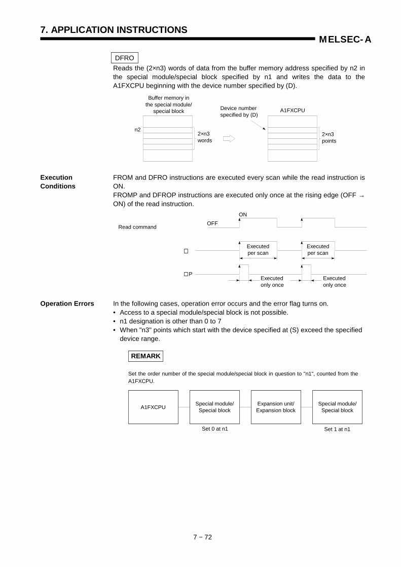
7. APPLICATION INSTRUCTIONS
7 − 72
MELSEC-A
DFROReads the (2×n3) words of data from the buffer memory address specified by n2 inthe special module/special block specified by n1 and writes the data to theA1FXCPU beginning with the device number specified by (D).
Execution FROM and DFRO instructions are executed every scan while the read instruction isConditions ON.
FROMP and DFROP instructions are executed only once at the rising edge (OFF →ON) of the read instruction.
Operation Errors In the following cases, operation error occurs and the error flag turns on.• Access to a special module/special block is not possible.• n1 designation is other than 0 to 7• When "n3" points which start with the device specified at (S) exceed the specified
device range.
REMARK
Set the order number of the special module/special block in question to "n1", counted from theA1FXCPU.
������������������������������������������������������������������������������������������������������������������������������������������������������������
������������������������������������������������������������������������������������������������������������������������������������������������������������
Buffer memory inthe special module/
special block A1FXCPU
n2
Device numberspecified by (D)
2×n3points
2×n3words
OFFON
Executedper scan
Executedper scan
Executedonly once
Executedonly once
P
Read command
A1FXCPU Expansion unit/Expansion block
Special module/Special block
Special module/Special block
Set 0 at n1 Set 1 at n1

7. APPLICATION INSTRUCTIONS
7 − 73
MELSEC-A
Program Example FROMThe program to read 1-word data from K2000 of buffer memory in the secondspecial module/special block from the A1FXCPU and writes the read data to D0when X20 is turned ON.
DFROThe program to read 2-word data from K2000 of buffer memory in the secondspecial module/special block from the A1FXCPU and writes the read data to D0 andD1 when X20 is turned ON.
REMARK
During the execution of the FROM/DFRO/TO/DTO instruction, M9119 can control the executionof an interruption program.• When M9119 is OFF (FROM/TO is given priority)
While the FROM/DFRO/TO/DTO instruction is executed, interrupt is disabled and interruptionprogram is not executed even at the occurrence of an interrupt.For the interrupt occurred during the execution of the FROM/DFRO/TO/DTO instruction, the interruption program that corresponds to the occurred interrupt is executed after the completion of the FROM/DFRO/TO/DTO instruction.While M9119 is OFF, the FROM/DFRO/TO/DTO instruction can be used in an interruption program.
• When M9119 is ON (interrupt is given priority)If an interrupt occurs during the execution of FROM/DFRO/TO/DTO instruction, execution of the FROM/DFRO/TO/DTO instruction is suspended and the interruption program that corresponds to the occurred interrupt is executed.While M9119 is OFF, the FROM/DFRO/TO/DTO instruction cannot be used in an interruption program.
• Objective interrupt is I0 to I5, I12, I13, and I29 to I31.
X0200
H K KFROM 0001 2000 D0 1
X0200
H K KDFRO 0001 2000 D0 1

MEMO
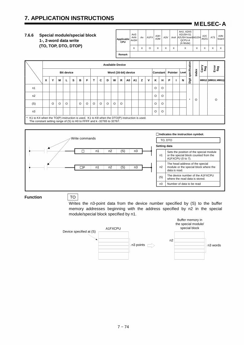
7. APPLICATION INSTRUCTIONS
7 − 74
MELSEC-A
7.6.6 Special module/special block1-, 2-word data write(TO, TOP, DTO, DTOP)
Available Device
Bit device Word (16-bit) device Constant Pointer Level Car
ryfla
g
Erro
rfla
g
X Y M L S B F T C D W R A0 A1 Z V K H P I N
Digi
t spe
cific
atio
n
Inde
x
M9012 (M9010, M9011)
n1 O O
n2 O O
(S) O O O O O O O O O O O O
n3 O O
* O O
*: K1 to K4 when the TO(P) instruction is used. K1 to K8 when the DTO(P) instruction is used.The constant setting range of (S) is H0 to FFFF and k -32765 to 32767.
Function TOWrites the n3-point data from the device number specified by (S) to the buffermemory addresses beginning with the address specified by n2 in the specialmodule/special block specified by n1.
AnSAnN
AnSHAn A1FX A3H
A3M A3V AnA
AnU, A2ASA2USH-S1
A2USH boardQCPU-A(A Mode)
A0J2H A2CA52G A73 A3N
boardApplicableCPU
X X O X X X X X X X X
Remark
n3
n3
n1Sets the position of the special moduleor the special block counted from theA1FXCPU (0 to 7).
n2The head address of the specialmodule or the special block where thedata is read.
(S) The device number of the A1FXCPUwhere the read data is stored.
n3 Number of data to be read
Setting data
TO, DTO
Indicates the instruction symbol.
n1 (S)
n1 (S)P
n2
n2
Write commands
������������������������������������������������������������������������������������������������������������������������������������������������������������
������������������������������������������������������������������������������������������������������������������������������������������������������������
Buffer memory inthe special module/
special blockA1FXCPU
n2
Device specified at (S)
n3 points n3 words
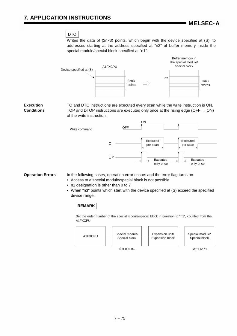
7. APPLICATION INSTRUCTIONS
7 − 75
MELSEC-A
DTOWrites the data of (2n×3) points, which begin with the device specified at (S), toaddresses starting at the address specified at "n2" of buffer memory inside thespecial module/special block specified at "n1".
Execution TO and DTO instructions are executed every scan while the write instruction is ON.Conditions TOP and DTOP instructions are executed only once at the rising edge (OFF → ON)
of the write instruction.
Operation Errors In the following cases, operation error occurs and the error flag turns on.• Access to a special module/special block is not possible.• n1 designation is other than 0 to 7• When "n3" points which start with the device specified at (S) exceed the specified
device range.
REMARK
Set the order number of the special module/special block in question to "n1", counted from theA1FXCPU.
������������������������������������������������������������������������������������������������������������������������������������������������������������
������������������������������������������������������������������������������������������������������������������������������������������������������������
Buffer memory inthe special module/
special blockA1FXCPU
n2
Device specified at (S)
2×n3points
2×n3words
OFF
ON
Executedper scan
Executedper scan
Executedonly once
Executedonly once
P
Write command
A1FXCPU Expansion unit/Expansion block
Special module/Special block
Special module/Special block
Set 0 at n1 Set 1 at n1
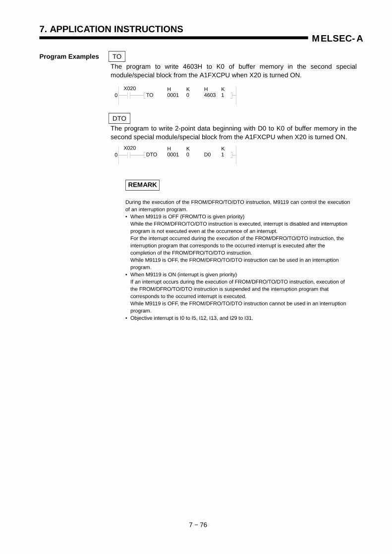
7. APPLICATION INSTRUCTIONS
7 − 76
MELSEC-A
Program Examples TOThe program to write 4603H to K0 of buffer memory in the second specialmodule/special block from the A1FXCPU when X20 is turned ON.
DTOThe program to write 2-point data beginning with D0 to K0 of buffer memory in thesecond special module/special block from the A1FXCPU when X20 is turned ON.
REMARK
During the execution of the FROM/DFRO/TO/DTO instruction, M9119 can control the executionof an interruption program.• When M9119 is OFF (FROM/TO is given priority)
While the FROM/DFRO/TO/DTO instruction is executed, interrupt is disabled and interruption program is not executed even at the occurrence of an interrupt.For the interrupt occurred during the execution of the FROM/DFRO/TO/DTO instruction, the interruption program that corresponds to the occurred interrupt is executed after the completion of the FROM/DFRO/TO/DTO instruction.While M9119 is OFF, the FROM/DFRO/TO/DTO instruction can be used in an interruption program.
• When M9119 is ON (interrupt is given priority)If an interrupt occurs during the execution of FROM/DFRO/TO/DTO instruction, execution of the FROM/DFRO/TO/DTO instruction is suspended and the interruption program that corresponds to the occurred interrupt is executed.While M9119 is OFF, the FROM/DFRO/TO/DTO instruction cannot be used in an interruption program.
• Objective interrupt is I0 to I5, I12, I13, and I29 to I31.
X0200
H K H KTO 0001 0 4603 1
X0200
H K KDTO 0001 0 D0 1

MEMO

7. APPLICATION INSTRUCTIONS
7 − 77
MELSEC-A
7.7 FOR to NEXT Instructions
7.7.1 FOR to NEXT (FOR, NEXT)
Available Device
Bit device Word (16-bit) device Constant Pointer Level Car
ryfla
g
Erro
rfla
g
X Y M L S B F T C D W R A0 A1 Z V K H P I N
Digi
t spe
cific
atio
n
Inde
x
M9012 (M9010, M9011)
n O O O O O O O O O O O O
Functions (1) When the processing of FOR to NEXT instructions is executed "n" timesunconditionally, performs the processing of the next step to the NEXT Instruction.
(2) At "n" , 1 to 32767 can be specified. When - 32767 to 0 has been specified, thesame processing an n = 1 is performed. (positive integers)
(3) When it is not desired to execute the processing of FOR to NEXT instructions,cause a jump by use of the CJ or SCJ instruction
ApplicableCPU All CPUs
FOR n
NEXT
Repeat program

7. APPLICATION INSTRUCTIONS
7 − 78
MELSEC-A
(4) Up to five levels of the nesting of FOR is allowed.
Operation Errors In the following cases, operation occurs and the PC stops its operation.• After the execution of FOR instruction, the END (FEND) instruction has been
executed before the NEXT instruction is executed.• The NEXT instruction has been executed before the FOR instruction is executed.• The number of the FOR instructions is different from that of the NEXT
instructions.• The JMP instruction is executed in the FOR to NEXT processing to exit from the
FOR to NEXT processing.• There is a STOP instruction in the FOR to NEXT processing.
Program Example FOR , NEXT(1) Program which executes the FOR to NEXT instructions when X8 is off and does
not execute the FOR to NEXT instructions when X8 is on.
NEXT
NEXT
NEXT
X000
X001
X002
Up to five levels of thenesting of FOR is allowed.
KFOR 5
KFOR 3
KFOR 100
( )
X008
M0
M0
0
4
10
13
22
23P8
CJ P8
K
FOR 4
INC Z
MOV Z D0
MOV 0 Z
Z
NEXT
Y033
• Coding0 LD X0081 CJ P84 LDI M05 MOV K0 Z
10 FOR K413 LDI M014 MOV Z D0Z19 INC Z22 NEXT23 P824 LD X00A25 OUT Y03326 ENDX00A
K

MEMO

7. APPLICATION INSTRUCTIONS
7 − 79
MELSEC-A
7.8 Local, Remote I/O Station Access Instructions
Local, remote I/O station access instructions are used to transfer data in a data linksystem.Four instructions are provided as shown below.The local and remote I/O station access instructions can be used in the sequenceprogram of the master station only.
Classification Instruction Symbol Ref. Page
Read LRDP 7-80Localstation Write LWTP 7-80
Read RFRP 7-86Remote I/Ostation Write RTOP 7-86
CAUTION
Local, remote I/O station access instructions (LRDP, LWTP, RFRP, RTQP) can be used onMELSECNET(II) and MELSECNET/B.They cannot be used on the MELSECNET/10.
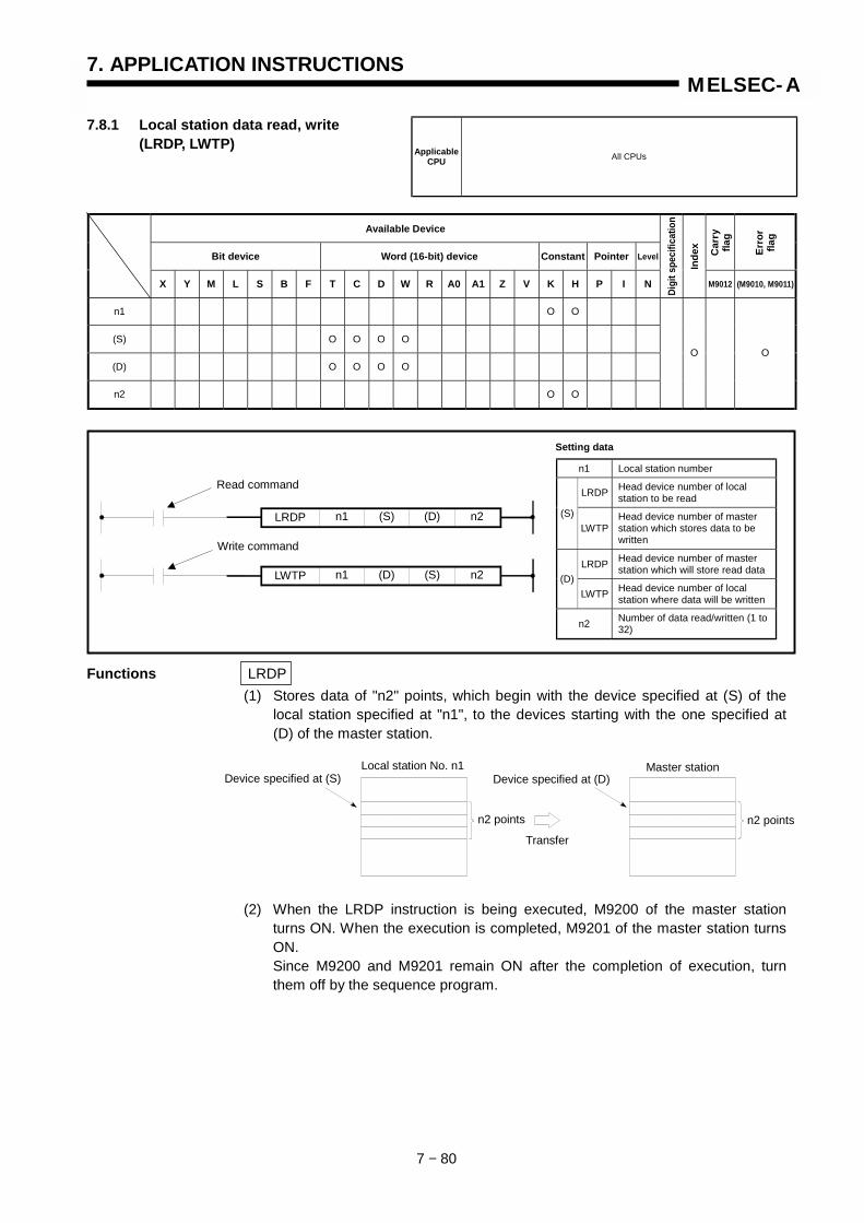
7. APPLICATION INSTRUCTIONS
7 − 80
MELSEC-A
7.8.1 Local station data read, write(LRDP, LWTP)
Available Device
Bit device Word (16-bit) device Constant Pointer Level Car
ryfla
g
Erro
rfla
g
X Y M L S B F T C D W R A0 A1 Z V K H P I N
Digi
t spe
cific
atio
n
Inde
x
M9012 (M9010, M9011)
n1 O O
(S) O O O O
(D) O O O O
n2 O O
O O
Functions LRDP(1) Stores data of "n2" points, which begin with the device specified at (S) of the
local station specified at "n1", to the devices starting with the one specified at(D) of the master station.
(2) When the LRDP instruction is being executed, M9200 of the master stationturns ON. When the execution is completed, M9201 of the master station turnsON.Since M9200 and M9201 remain ON after the completion of execution, turnthem off by the sequence program.
ApplicableCPU All CPUs
LRDP n1 (S) (D) n2
LWTP n1 (D) (S) n2
Write command
Read commandn1 Local station number
LRDP Head device number of localstation to be read
(S)LWTP
Head device number of masterstation which stores data to bewritten
LRDP Head device number of masterstation which will store read data
(D)LWTP Head device number of local
station where data will be written
n2 Number of data read/written (1 to32)
Setting data
Master station
���������������������������������������������������������������������������������������������������������������������
���������������������������������������������������������������������������������������������������������������������
Device specified at (S)Local station No. n1
Device specified at (D)
n2 points
Transfer
n2 points
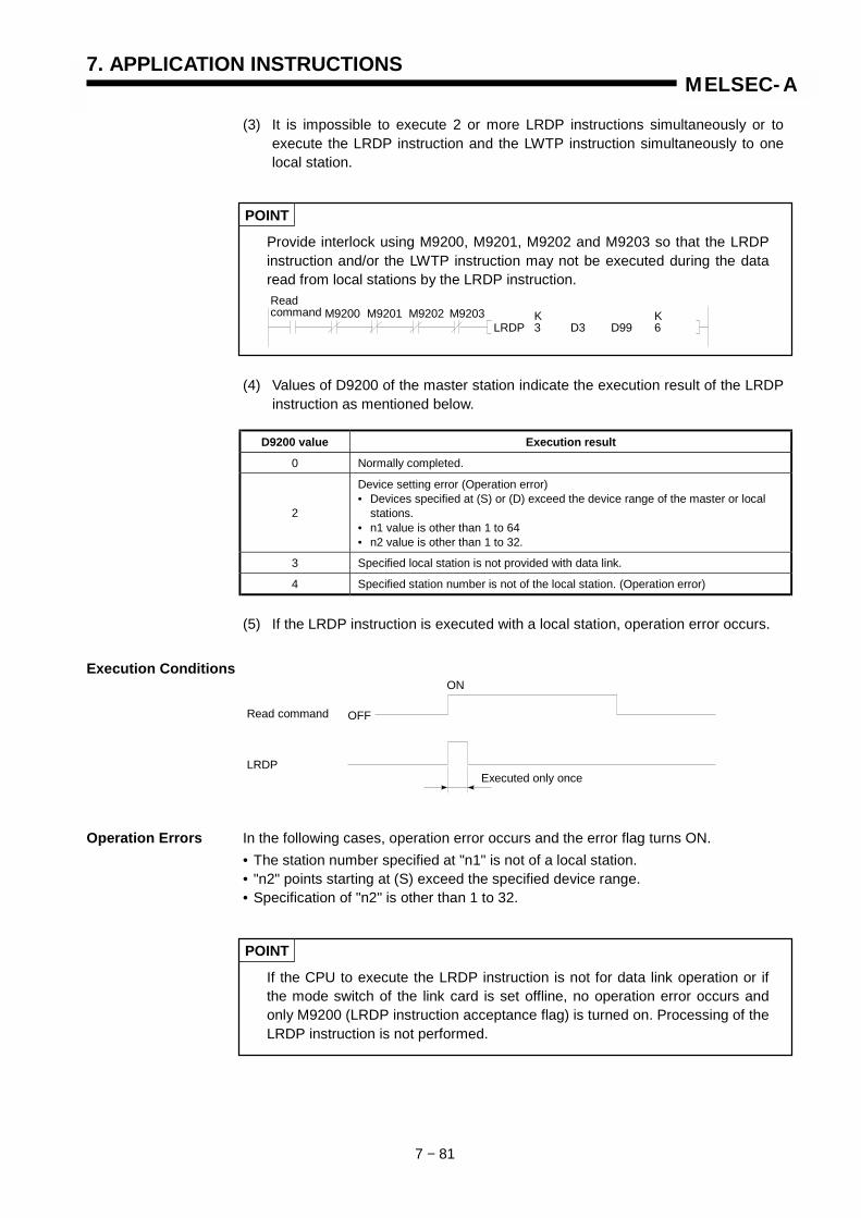
7. APPLICATION INSTRUCTIONS
7 − 81
MELSEC-A
(3) It is impossible to execute 2 or more LRDP instructions simultaneously or toexecute the LRDP instruction and the LWTP instruction simultaneously to onelocal station.
POINT
Provide interlock using M9200, M9201, M9202 and M9203 so that the LRDPinstruction and/or the LWTP instruction may not be executed during the dataread from local stations by the LRDP instruction.
(4) Values of D9200 of the master station indicate the execution result of the LRDPinstruction as mentioned below.
D9200 value Execution result
0 Normally completed.
2
Device setting error (Operation error)• Devices specified at (S) or (D) exceed the device range of the master or local
stations.• n1 value is other than 1 to 64• n2 value is other than 1 to 32.
3 Specified local station is not provided with data link.
4 Specified station number is not of the local station. (Operation error)
(5) If the LRDP instruction is executed with a local station, operation error occurs.
Execution Conditions
Operation Errors In the following cases, operation error occurs and the error flag turns ON.• The station number specified at "n1" is not of a local station.• "n2" points starting at (S) exceed the specified device range.• Specification of "n2" is other than 1 to 32.
POINT
If the CPU to execute the LRDP instruction is not for data link operation or ifthe mode switch of the link card is set offline, no operation error occurs andonly M9200 (LRDP instruction acceptance flag) is turned on. Processing of theLRDP instruction is not performed.
Readcommand M9200 M9201 M9202 M9203 K K
LRDP 3 D3 D99 6
Read command
Executed only onceLRDP
OFF
ON

7. APPLICATION INSTRUCTIONS
7 − 82
MELSEC-A
Program Examples LRDPA program to store data of D3 to D8 of the 3rd local station in D99 to D104 of themaster station when X3 is ON.
*1: The contact which corresponds to M1 shown in the program example should be converted into a pulse. If a pulse is not used, following execution of the LRDP instruction will be disabled.
*2: The contact which corresponds to M0 shown in the program example should be turned ON by the SET instruction. If the OUT or PLS instruction is used, the LRDP instruction may often be executedincorrectly.
• Coding0 LD X0031 PLS M14 LD M15 SET M06 LD M07 MPS8 ANI M92009 ANI M9201
10 ANI M920211 ANI M920312 LRDP K3 D3 D99 K623 MPP24 AND M920125 RST M026 RST M920029 RST M920132 END
Use a pulse signal forthis command. (*1)
Provide interlock usingthe LRDP instructionexecution flag.
If the LWTP instruction is used to the same station,provide interlock using the LWTP instruction execution flag.
X003
M1
M0 M9200 M9201 M9202 M9203
PLS M1
K KLRDP 3 D3 D99 6
M9201
SET M0
RST M0
RST M9200
RST M9201
(*2)
When X3 is ON, M0 turns ON.
If the LRDP and LWTP instructions are not beingexecuted when M0 is ON, the LRDP instructionfor the 3rd station is executed, and M9200 isturned ON.
At read completion, M0, M9200 and M9201 areturned OFF.
0
4
6
Turned OFF by thesequence program.
Turned OFF by thesequence program.
Turned ON bythe PC CPU.
Executed only once.
Executed only once.
M9200
M9201
M0
M1
X3
LRDP
OFF
OFF
OFF
OFF
ON
ON
ON
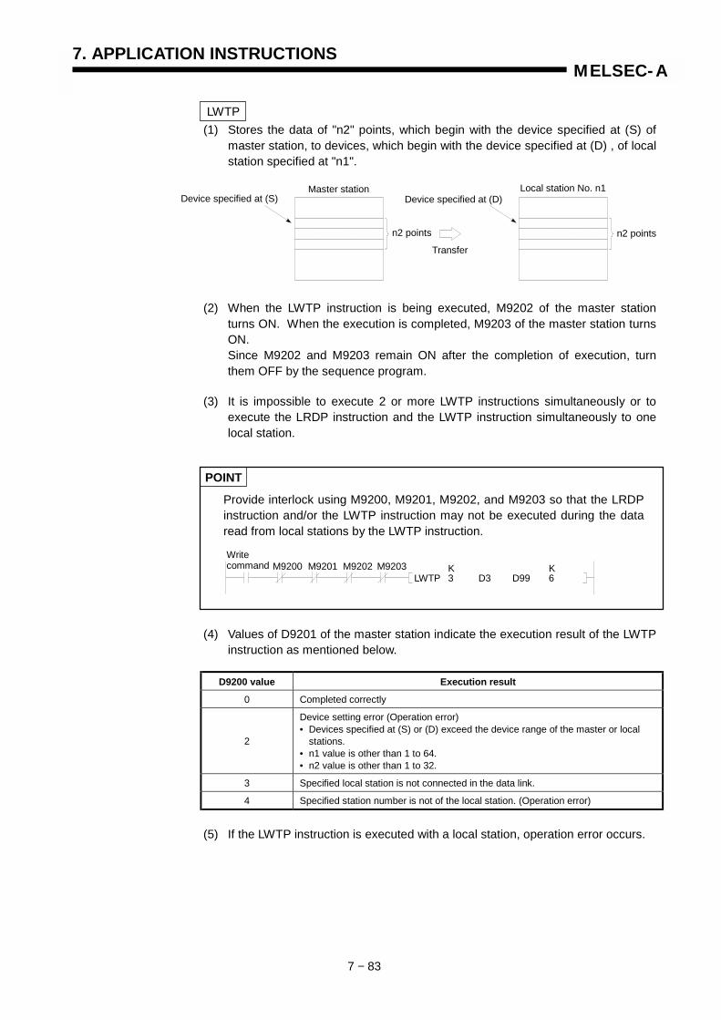
7. APPLICATION INSTRUCTIONS
7 − 83
MELSEC-A
LWTP(1) Stores the data of "n2" points, which begin with the device specified at (S) of
master station, to devices, which begin with the device specified at (D) , of localstation specified at "n1".
(2) When the LWTP instruction is being executed, M9202 of the master stationturns ON. When the execution is completed, M9203 of the master station turnsON.Since M9202 and M9203 remain ON after the completion of execution, turnthem OFF by the sequence program.
(3) It is impossible to execute 2 or more LWTP instructions simultaneously or toexecute the LRDP instruction and the LWTP instruction simultaneously to onelocal station.
POINT
Provide interlock using M9200, M9201, M9202, and M9203 so that the LRDPinstruction and/or the LWTP instruction may not be executed during the dataread from local stations by the LWTP instruction.
(4) Values of D9201 of the master station indicate the execution result of the LWTPinstruction as mentioned below.
D9200 value Execution result
0 Completed correctly
2
Device setting error (Operation error)• Devices specified at (S) or (D) exceed the device range of the master or local
stations.• n1 value is other than 1 to 64.• n2 value is other than 1 to 32.
3 Specified local station is not connected in the data link.
4 Specified station number is not of the local station. (Operation error)
(5) If the LWTP instruction is executed with a local station, operation error occurs.
Master station���������������������������������������������������������������������������������������������������������������������
���������������������������������������������������������������������������������������������������������������������
Device specified at (S)Local station No. n1
Device specified at (D)
n2 points
Transfer
n2 points
Writecommand M9200 M9201 M9202 M9203 K K
LWTP 3 D3 D99 6

7. APPLICATION INSTRUCTIONS
7 − 84
MELSEC-A
Execution Conditions
Operation Errors In the following cases, operation error occurs and the error flag turns on.• The station number specified at "n1" is not a local station.• "n2" points starting at (D) exceed the specified device range.• Specification of "n2" is other than 1 to 32.
POINT
If an LWTP instruction is executed by a CPU which is not for data link, orwhen the mode select switch for the link card is set for OFFLINE, no operationerror occurs and M9202 (LWTP instruction enable flag) is set without theLWTP instruction processing.
Write command
Executed only onceLWTP
ON
OFF
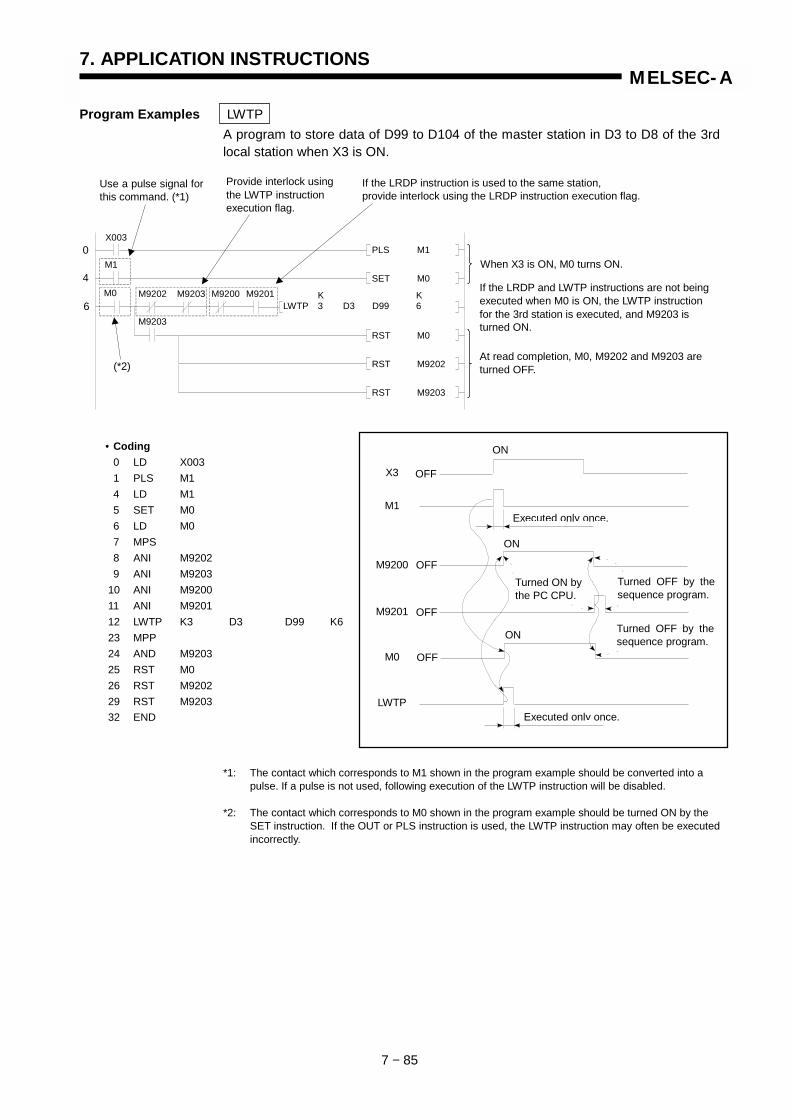
7. APPLICATION INSTRUCTIONS
7 − 85
MELSEC-A
Program Examples LWTPA program to store data of D99 to D104 of the master station in D3 to D8 of the 3rdlocal station when X3 is ON.
*1: The contact which corresponds to M1 shown in the program example should be converted into a pulse. If a pulse is not used, following execution of the LWTP instruction will be disabled.
*2: The contact which corresponds to M0 shown in the program example should be turned ON by the SET instruction. If the OUT or PLS instruction is used, the LWTP instruction may often be executedincorrectly.
Use a pulse signal forthis command. (*1)
Provide interlock usingthe LWTP instructionexecution flag.
If the LRDP instruction is used to the same station,provide interlock using the LRDP instruction execution flag.
X003
M1
M0 M9202 M9203 M9200 M9201
PLS M1
K KLWTP 3 D3 D99 6
M9203
SET M0
RST M0
RST M9202
RST M9203
(*2)
When X3 is ON, M0 turns ON.
If the LRDP and LWTP instructions are not beingexecuted when M0 is ON, the LWTP instructionfor the 3rd station is executed, and M9203 isturned ON.
At read completion, M0, M9202 and M9203 areturned OFF.
0
4
6
• Coding0 LD X0031 PLS M14 LD M15 SET M06 LD M07 MPS8 ANI M92029 ANI M9203
10 ANI M920011 ANI M920112 LWTP K3 D3 D99 K623 MPP24 AND M920325 RST M026 RST M920229 RST M920332 END
Turned OFF by thesequence program.
Turned OFF by thesequence program.
Turned ON bythe PC CPU.
Executed only once.
Executed only once.
M9200
M9201
M0
M1
X3
LWTP
OFF
OFF
OFF
OFF
ON
ON
ON

7. APPLICATION INSTRUCTIONS
7 − 86
MELSEC-A
7.8.2 Remote I/O station data read, Write(RFRP, RTOP)
Available Device
Bit device Word (16-bit) device Constant Pointer Level Car
ryfla
g
Erro
rfla
g
X Y M L S B F T C D W R A0 A1 Z V K H P I N
Digi
t spe
cific
atio
n
Inde
x
M9012 (M9010, M9011)
n1 O O
n2 O O
(S) O
(D) O
n3 O O
O O
REMARK
• (n1) is specified by the head I/O number of special function module when viewed from the master station.
Example)Remote I/O station No. 2 is assigned by parameters to X100 to X17F and Y140 to Y190.
AnSAnN
AnSHAn A1FX A3H
A3M A3V AnA
AnU, A2ASA2USH-S1
A2USH boardQCPU-A(A Mode)
A0J2H A2CA52G A73 A3N
boardApplicableCPU
O O O O X O O O O O O
Remark
RFRP n1 n2 (D) n3
RTOP n1 n2 (S) n3
Write command
Read commandn1
Head I/O number of specialfunction module specified bymaster station.
RFRPHead address inside intelligentmodule which stores data to bereadn2
RTOP Address inside special functionmodule where data will be written
(D) RFRP Head number of link registerwhich will store read data
(S) RTOP Head number of link registerwhich stores data to be written
n3 Number of data read/written (1 to16)
Setting data
X100
X10F
X110
X11F
X120
X12F
X130
X13F
140
15F
160
17F
Y180
Y18F
Y190
Y19F
to to to to to to to to
X000
X00F
X010
X01F
X020
X02F
X030
X03F
040
05F
060
07F
Y080
Y08F
Y090
Y09F
to to to to to to to toStationNo.2
To other station
To other station
Head I/O number: H140
Use these in the RFRP/RTOP instructions.
I/O numbers viewed fromthe master station
I/O numbers of the station
Pow
er s
uppi
ym
odul
eR
emot
e I/O
mod
ule
AX1
0
AX1
0
AX1
0
A68A
D
AD71
AY10
AY10
AX1
0
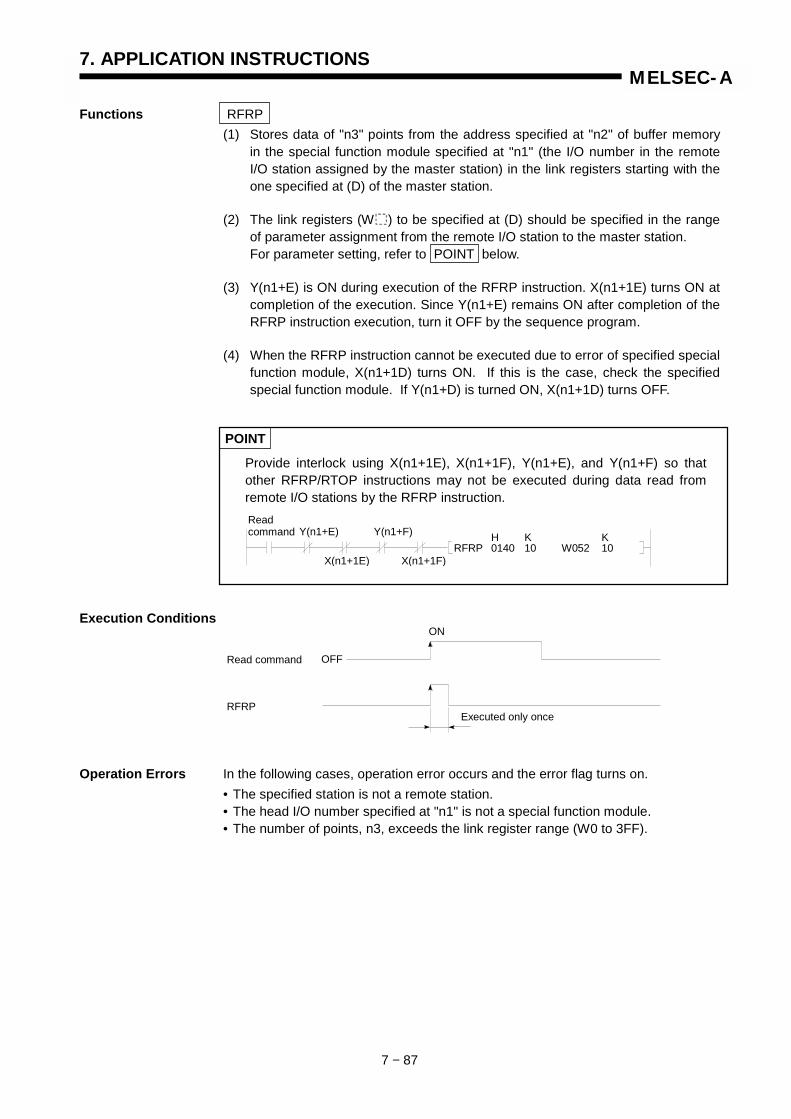
7. APPLICATION INSTRUCTIONS
7 − 87
MELSEC-A
Functions RFRP(1) Stores data of "n3" points from the address specified at "n2" of buffer memory
in the special function module specified at "n1" (the I/O number in the remoteI/O station assigned by the master station) in the link registers starting with theone specified at (D) of the master station.
(2) The link registers (W ) to be specified at (D) should be specified in the rangeof parameter assignment from the remote I/O station to the master station.For parameter setting, refer to POINT below.
(3) Y(n1+E) is ON during execution of the RFRP instruction. X(n1+1E) turns ON atcompletion of the execution. Since Y(n1+E) remains ON after completion of theRFRP instruction execution, turn it OFF by the sequence program.
(4) When the RFRP instruction cannot be executed due to error of specified specialfunction module, X(n1+1D) turns ON. If this is the case, check the specifiedspecial function module. If Y(n1+D) is turned ON, X(n1+1D) turns OFF.
POINT
Provide interlock using X(n1+1E), X(n1+1F), Y(n1+E), and Y(n1+F) so thatother RFRP/RTOP instructions may not be executed during data read fromremote I/O stations by the RFRP instruction.
Execution Conditions
Operation Errors In the following cases, operation error occurs and the error flag turns on.• The specified station is not a remote station.• The head I/O number specified at "n1" is not a special function module.• The number of points, n3, exceeds the link register range (W0 to 3FF).
Readcommand Y(n1+E) Y(n1+F) H K K
RFRP 0140 10 W052 10X(n1+1E) X(n1+1F)
Read command
Executed only onceRFRP
OFF
ON
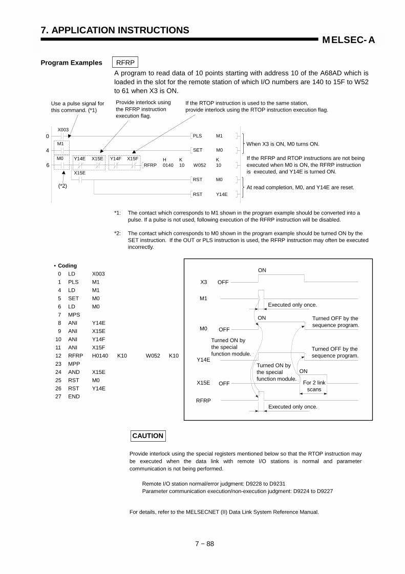
7. APPLICATION INSTRUCTIONS
7 − 88
MELSEC-A
Program Examples RFRPA program to read data of 10 points starting with address 10 of the A68AD which isloaded in the slot for the remote station of which I/O numbers are 140 to 15F to W52to 61 when X3 is ON.
*1: The contact which corresponds to M1 shown in the program example should be converted into a pulse. If a pulse is not used, following execution of the RFRP instruction will be disabled.
*2: The contact which corresponds to M0 shown in the program example should be turned ON by the SET instruction. If the OUT or PLS instruction is used, the RFRP instruction may often be executedincorrectly.
CAUTION
Provide interlock using the special registers mentioned below so that the RTOP instruction maybe executed when the data link with remote I/O stations is normal and parametercommunication is not being performed.
Remote I/O station normal/error judgment: D9228 to D9231Parameter communication execution/non-execution judgment: D9224 to D9227
For details, refer to the MELSECNET (II) Data Link System Reference Manual.
• Coding0 LD X0031 PLS M14 LD M15 SET M06 LD M07 MPS8 ANI Y14E9 ANI X15E
10 ANI Y14F11 ANI X15F12 RFRP H0140 K10 W052 K1023 MPP24 AND X15E25 RST M026 RST Y14E27 END
0
4
6
Use a pulse signal forthis command. (*1)
Provide interlock usingthe RFRP instructionexecution flag.
If the RTOP instruction is used to the same station,provide interlock using the RTOP instruction execution flag.
X003
M1
M0 Y14E X15E Y14F X15F
X15E
PLS M1
H K KRFRP 0140 10 W052 10
SET M0
RST M0
RST Y14E
When X3 is ON, M0 turns ON.
If the RFRP and RTOP instructions are not beingexecuted when M0 is ON, the RFRP instructionis executed, and Y14E is turned ON.
At read completion, M0, and Y14E are reset.(*2)
Executed only once.
Turned OFF by thesequence program.
Turned ON bythe specialfunction module.
For 2 linkscans
Executed only once.
Turned OFF by thesequence program.
Turned ON bythe specialfunction module.
RFRP
X15E
Y14E
M0
M1
X3
ON
ON
ON
OFF
OFF
OFF

7. APPLICATION INSTRUCTIONS
7 − 89
MELSEC-A
Functions RTOP(1) Writes data of "n3" points of the link registers (W ) starting with the one
specified at (S) to addresses starting with the one specified at "n2" of buffermemory in the special function module of which I/O number is specified at "n1"(the I/O number in the remote I/O station assigned by the master station).
(2) The link registers (W ) to be specified at (S) should be specified in the rangeof parameter assignment from the master station to the remote I/O station.For parameter setting, refer to POINT below.
(3) It is not allowed to use two or more RTOP instructions or to use the RTOP andRFRP instructions simultaneously with a special function module which has thesame I/O number.
POINT
Provide interlock using X(n1+1E), X(n1+1F), Y(n1+E), and Y(n1+F) so thatother RTOP instructions may not be executed during data write to remote I/Ostations by the RTOP instruction.
(4) Y(n1+F) is ON during execution of the RTOP instruction. X(n1+1F) turns ON atcompletion of the execution. Since Y(n1+F) remains ON after completion of theRTOP instruction execution, turn it OFF by the sequence program.
(5) When the RTOP instruction cannot be executed due to error of specified specialfunction module, X(n1+1D) turns ON. If this is the case, check the specifiedspecial function module. If Y(n1+D) is turned ON, X(n1+1D) turns OFF.
Execution Conditions
Operation Errors In the following cases, operation error occurs and the error flag turns on.• The specified station is not a remote station.• The head I/O number specified at "n1" is not a special function module.• The number of points, n3, exceeds the link register range (W0 to 3FF).
Write instructionY(n1+F) Y(n1+E) H K K
RTOP 0140 10 W052 10X(n1+1F) X(n1+1E)
Read command
Executed only onceRFRP
OFF
ON

7. APPLICATION INSTRUCTIONS
7 − 90
MELSEC-A
Program Examples RTOPA program to write data in W52 to 61 to addresses of 10 points starting with address10 in the A68AD which is loaded in the slot for the remote station of which I/Onumbers are 140 to 15F when X3 is ON.
*1: The contact which corresponds to M1 shown in the program example should be converted into a pulse. If a pulse is not used, following execution of the RTOP instruction will be disabled.
*2: The contact which corresponds to M0 shown in the program example should be turned ON by the SET instruction. If the OUT or PLS instruction is used, the RTOP instruction may often be executedincorrectly.
CAUTION
Provide interlock using the special registers mentioned below so that the RTOP instruction maybe executed when the data link with remote I/O stations is normal and parametercommunication is not being performed.
Remote I/O station normal/error judgment: D9228 to D9231Parameter communication execution/non-execution judgment: D9224 to D9227
For details, refer to the MELSECNET (II) Data Link System Reference Manual.
• Coding0 LD X0031 PLS M14 LD M15 SET M06 LD M07 MPS8 ANI Y14F9 ANI X15F
10 ANI Y14E11 ANI X15E12 RTOP H0140 K10 W052 K1023 MPP24 AND X15F25 RST M026 RST Y14F27 END
Turned OFF by thesequence program.
Turned OFF by thesequence program.
Use a pulse signal forthis command. (*1)
Provide interlock usingthe RTOP instructionexecution flag.
If the RTOP instruction is used to the same station,provide interlock using the RTOP instruction execution flag.
X003
M1
M0
0
4
6Y14F X15F Y14E X15E
X15F
PLS M1
H K KRTOP 0140 10 W052 10
SET M0
RST M0
RST Y14F
When X3 is ON, M0 turns ON.
If the RFRP and RTOP instructions are not beingexecuted when M0 is ON, the RTOP instructionis executed, and Y10F is turned on.
At read completion, X11F turns on, and M0 andY10F are reset.
(*2)
Executed only once.
Turned ON bythe specialfunction module.
For 2 linkscans
Executed only once.
Turned ON bythe specialfunction module.
RTOP
X11E
Y10E
M0
M1
X3
ON
ON
ON
OFF
OFF
OFF
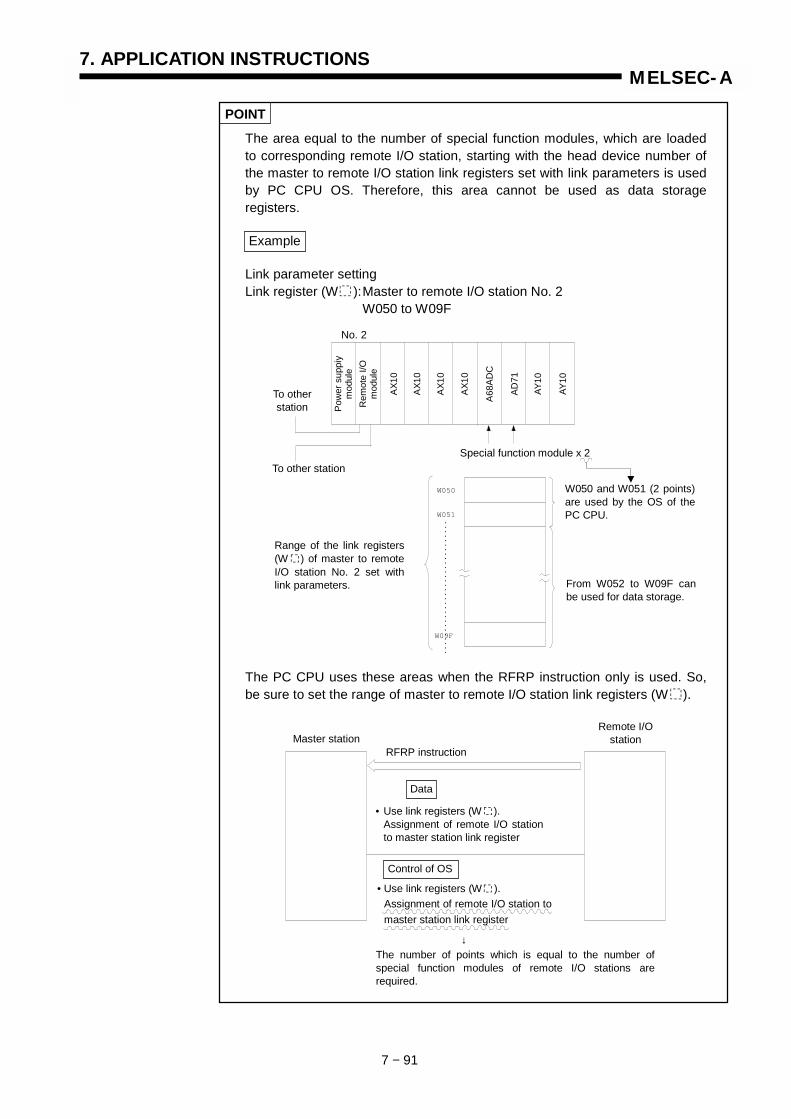
7. APPLICATION INSTRUCTIONS
7 − 91
MELSEC-A
POINT
The area equal to the number of special function modules, which are loadedto corresponding remote I/O station, starting with the head device number ofthe master to remote I/O station link registers set with link parameters is usedby PC CPU OS. Therefore, this area cannot be used as data storageregisters.
Example
Link parameter settingLink register (W ):Master to remote I/O station No. 2
W050 to W09F
The PC CPU uses these areas when the RFRP instruction only is used. So,be sure to set the range of master to remote I/O station link registers (W ).
Master stationRFRP instruction
Remote I/Ostation
Data
Control of OS
The number of points which is equal to the number ofspecial function modules of remote I/O stations arerequired.
↓
• Use link registers (W ).Assignment of remote I/O stationto master station link register
• Use link registers (W ).Assignment of remote I/O station tomaster station link register
No. 2
To other stationSpecial function module x 2
To otherstation
W050 and W051 (2 points)are used by the OS of thePC CPU.
From W052 to W09F canbe used for data storage.
Range of the link registers(W ) of master to remoteI/O station No. 2 set withlink parameters.
W050
W051
W09F
..............................
Pow
er s
uppi
ym
odul
eR
emot
e I/O
mod
ule
AX1
0
AX1
0
AX1
0
AX1
0
A68A
DC
AD71
AY10
AY10
7. APPLICATION INSTRUCTIONS
7 − 92
MELSEC-A
7.9 Display Instructions
(1) Display instructions are used to output ASCII codes to the output modules, to display data on the LED display on the front panel of the CPU module and to reset the annunciator.
(2) The display instructions are available in the following seven types.
Classification Instruction Symbol Ref. Page
PR 7-94ASCII code output
PRC 7-94
LED 7-100
LEDC 7-100
LEDA 7-103Display
LEDB 7-103
Display reset LEDR 7-105
POINT
The LEDA and LEDB instructions cannot be used with the A3A, A3U andA4U. (Their use is changed to the start command for dedicated instructions.)To perform processings equivalent to the LEDA and LEDB instructions withthe A3A, A3U and A4U, edit character string data using dedicated instructionsprovided for the AnA, AnU before using the LED instruction.
(3) The priority of display at the LED indicator is as indicated below.
Priority: High 1) Display due to self-diagnostic error2) Display due to CHK.3) Display of annunciator (F) number4) Display due to LED, LEDC, LEDA, or LEDB
Low 5) BATTERY ERROR
The above priority can be changed on the A3A, A3U and A4U.For details, refer to the A2A(S1)/A3ACPU User's Manual or the A2U (S1)/A3U/A4UCPU User’s Manual.
(4) When there is a display at the LED indicator due to 1 to 3, the execution ofdisplay instruction does not change the display. When there is a display at theLED indicator due to 5, the execution of display instruction provides the displayof that display instruction.
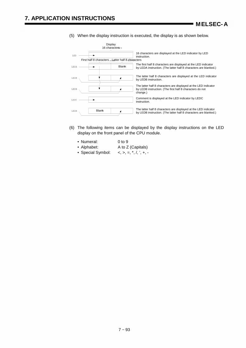
7. APPLICATION INSTRUCTIONS
7 − 93
MELSEC-A
(5) When the display instruction is executed, the display is as shown below.
(6) The following items can be displayed by the display instructions on the LEDdisplay on the front panel of the CPU module.
• Numeral: 0 to 9• Alphabet: A to Z (Capitals)• Special Symbol: <, >, =, *, /, ’, +, -
LED
LEDB
LEDB
Display
LEDC
LEDB
LEDA Blank
Blank
16 characters
First half 8 charactersLatter half 8
16 characters are displayed at the LED indicator by LEDinstruction.
The first half 8 characters are displayed at the LED indicatorby LEDA instruction. (The latter half 8 characters are blanked.)
The latter half 8 characters are displayed at the LED indicatorby LEDB instruction.
The latter half 8 characters are displayed at the LED indicatorby LEDB instruction. (The first half 8 characters do notchange.)
Comment is displayed at the LED indicator by LEDCinstruction.
The latter half 8 characters are displayed at the LED indicatorby LEDB instruction. (The latter half 8 characters are blanked.)
Display16 characters
First half 8 characters Latter half 8 characters
Blank
Blank

7. APPLICATION INSTRUCTIONS
7 − 94
MELSEC-A
7.9.1 ASCII code print instructions(PR, PRC)
Available Device
Bit device Word (16-bit) device Constant Pointer Level Car
ryfla
g
Erro
rfla
g
X Y M L S B F T C D W R A0 A1 Z V K H P I N
Digi
t spe
cific
atio
n
Inde
x
M9012 (M9010, M9011)
(S) O O O O OPR
(D) OO
(S) O O O O O O O O O O O O O OPRC
(D) O
O
Functions PRThe PR instruction has the following two functions.• Outputs an ASCII code of 16 characters stored in units of eight points beginning
with the device specified at (S), to the output module specified at (D).• Outputs an ASCII code from the device specified at (S) to 00H code to the output
module specified at (D).
Note that the second function cannot be used with the An and A3V.These functions can be switched by ON/OFF setting of M9049.
CPUs other than An and A3VAn, A3V
M9049 ON M9049 OFF
Output of 16 characters O O X
Output to 00H code X X O
AnSAnN
AnSHAn A1FX A3H
A3M A3V AnA
AnU, A2ASA2USH-S1
A2USH boardQCPU-A(A Mode)
A0J2H A2CA52G A73 A3N
boardApplicableCPU
O O O O O O X O O
Remark * With a PR instruction, only output of 16 characters in the ASCII code is possible.
* *
(S) Head number of device whichstores ASCII code
PR(D) Head number of output unit
which outputs ASCII code
(S) Device number which printscomment
PRC(D) Head number of output unit
which outputs comment
Setting data PR, PRC
Indicates the instruction symbol.
ASCII print command
(S) (D)

7. APPLICATION INSTRUCTIONS
7 − 95
MELSEC-A
(1) ASCII code output of 16 characters1) The number of points used for the output module is 10 points which start at
the Y number specified at (D).
2) The output signal from the output module is sent at 30ms per character.Therefore, 480ms (=16×30ms) is required until 16 characters are sent.However, since the control during sending is performed by the interruptprocessing at intervals of 10ms, the sequence processing is performedcontinuously.10 points beginning with the Y number specified in D are provided to theoutput unit during sequence processing, irrespective of I/O refresh afterEND.
3) In addition to the ASCII code, a strobe signal (10 msec ON, 20 msec OFF) isalso output from the device specified at (D) + 8.
4) Until the execution of sending the ASCII code of 16 characters afterexecution of the PR instruction, the PR instruction execution flag (device(D)+9) is ON.
5) Multiple PR and PRC instructions can be used. In such a case, however,provide interlock by use of the PR instruction execution flag (contact ofdevice (D)+9) so that the instructions may not turn on at the same time.
41H42H
43H44H
45H46H
47H48H
4BH4CH
4DH4EH
4FH50H
49H4AH
(D)
(D)+7
(D)+8
(D)+9
(S)+0
(S)+1
(S)+2
(S)+3
(S)+4
(S)+5
(S)+6
(S)+7
50H
4FH
4EH
4DH
to
4CH
4BH
4AH
49H
48H
47H
46H
45H
44H
43H
42H
41H
Device which store ASCII code
PR instruction execution flag(used for interlocking)
Sequenceprogram
Output Y
Strobe signal output
ASCII code outputPrinter orindicator
Head ofoutput
Upper 8 bits Lower 8 bits
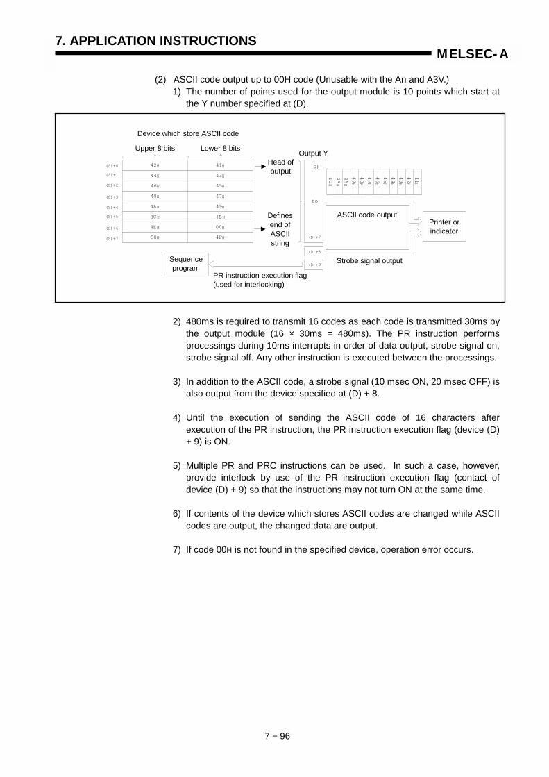
7. APPLICATION INSTRUCTIONS
7 − 96
MELSEC-A
(2) ASCII code output up to 00H code (Unusable with the An and A3V.)1) The number of points used for the output module is 10 points which start at
the Y number specified at (D).
2) 480ms is required to transmit 16 codes as each code is transmitted 30ms bythe output module (16 × 30ms = 480ms). The PR instruction performsprocessings during 10ms interrupts in order of data output, strobe signal on,strobe signal off. Any other instruction is executed between the processings.
3) In addition to the ASCII code, a strobe signal (10 msec ON, 20 msec OFF) isalso output from the device specified at (D) + 8.
4) Until the execution of sending the ASCII code of 16 characters afterexecution of the PR instruction, the PR instruction execution flag (device (D)+ 9) is ON.
5) Multiple PR and PRC instructions can be used. In such a case, however,provide interlock by use of the PR instruction execution flag (contact ofdevice (D) + 9) so that the instructions may not turn ON at the same time.
6) If contents of the device which stores ASCII codes are changed while ASCIIcodes are output, the changed data are output.
7) If code 00H is not found in the specified device, operation error occurs.
41H42H
43H44H
45H46H
47H48H
4BH4CH
00H4EH
4FH50H
49H4AH
(D)
(D)+7
(D)+8
(D)+9
(S)+0
(S)+1
(S)+2
(S)+3
(S)+4
(S)+5
(S)+6
(S)+7
to
4CH
4BH
4AH
49H
48H
47H
46H
45H
44H
43H
42H
41H
PR instruction execution flag(used for interlocking)
Sequenceprogram
Output Y
Strobe signal output
ASCII code outputPrinter orindicator
Head ofoutput
Definesend ofASCIIstring
Device which store ASCII code
Upper 8 bits Lower 8 bits

7. APPLICARTION INSTRUCTIONS
7 − 97
MELSEC-A
PRC(1) Outputs the comment (ASCII code) of the device specified at (S) to the output
module specified at (D). The number of points used for the output module iseight points which start at the Y number specified at (D).
(2) 480ms is required to transmit 16 codes as each code is transmitted 30ms bythe output module (16×30 ms=480 ms). The PRC instruction performs process-ings during 10ms interrupts in order of data output, strobe signal on, strobesignal off. Any other instruction is executed between the processings.
(3) In addition to the ASCII code, a strobe signal (10 msec ON, 20 msec OFF) isalso output from the device specified at (D) +8.
(4) Until the execution of sending the ASCII code of 16 characters after executionof the PRC instruction, the PRC instruction execution flag (device (D) +9) is ON.
(5) Multiple PR and PRC instructions can be used. In such a case, however,provide interlock by use of the PRC instruction execution flag (contact of device(D) +9) so that the instructions may not turn ON at the same time.
A B C D E F G H I J K L M N O
Y30X1PRC
Y30
Y37
Y38
Y39
to
PRC instruction execution flag(used for interlocking)
ASCII code output
Strobe signal output
Output Y
Printer orindicator
Comment of ×1
Head of output
Sequenceprogram
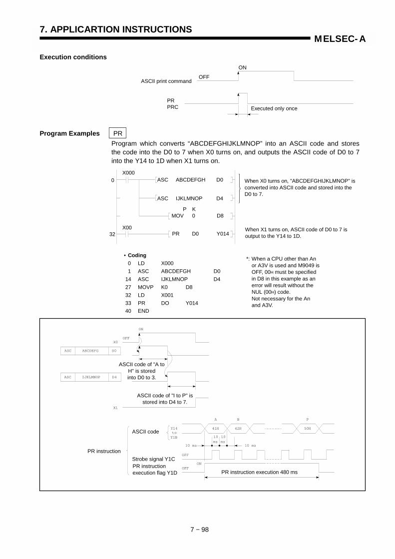
7. APPLICARTION INSTRUCTIONS
7 − 98
MELSEC-A
Execution conditions
Program Examples PRProgram which converts “ABCDEFGHIJKLMNOP” into an ASCII code and storesthe code into the D0 to 7 when X0 turns on, and outputs the ASCII code of D0 to 7into the Y14 to 1D when X1 turns on.
• Coding0 LD X0001 ASC ABCDEFGH D0
14 ASC IJKLMNOP D427 MOVP K0 D832 LD X00133 PR DO Y01440 END
*: When a CPU other than Anor A3V is used and M9049 isOFF, 00H must be specifiedin D8 in this example as anerror will result without theNUL (00H) code.Not necessary for the Anand A3V.
Y14
Y1B 10ms
10ms
10 ms
41H 42H 50H
A B P
10 ms
OFF
ONOFF
ASC IJKLMNOP D4
X0
X1
OFF
ON
ASC ABCDEFG D0
to
ASCII code of "A toH" is storedinto D0 to 3.
ASCII code of "I to P" isstored into D4 to 7.
ASCII code
PR instructionStrobe signal Y1CPR instructionexecution flag Y1D PR instruction execution 480 ms
OFF
ON
Executed only oncePRPRC
ON
OFFASCII print command
32X00
X000When X0 turns on, "ABCDEFGHIJKLMNOP" isconverted into ASCII code and stored into theD0 to 7.
When X1 turns on, ASCII code of D0 to 7 isoutput to the Y14 to 1D.
ASC ABCDEFGH D0
ASC IJKLMNOP D4
P KMOV 0 D8
PR D0 Y014
0
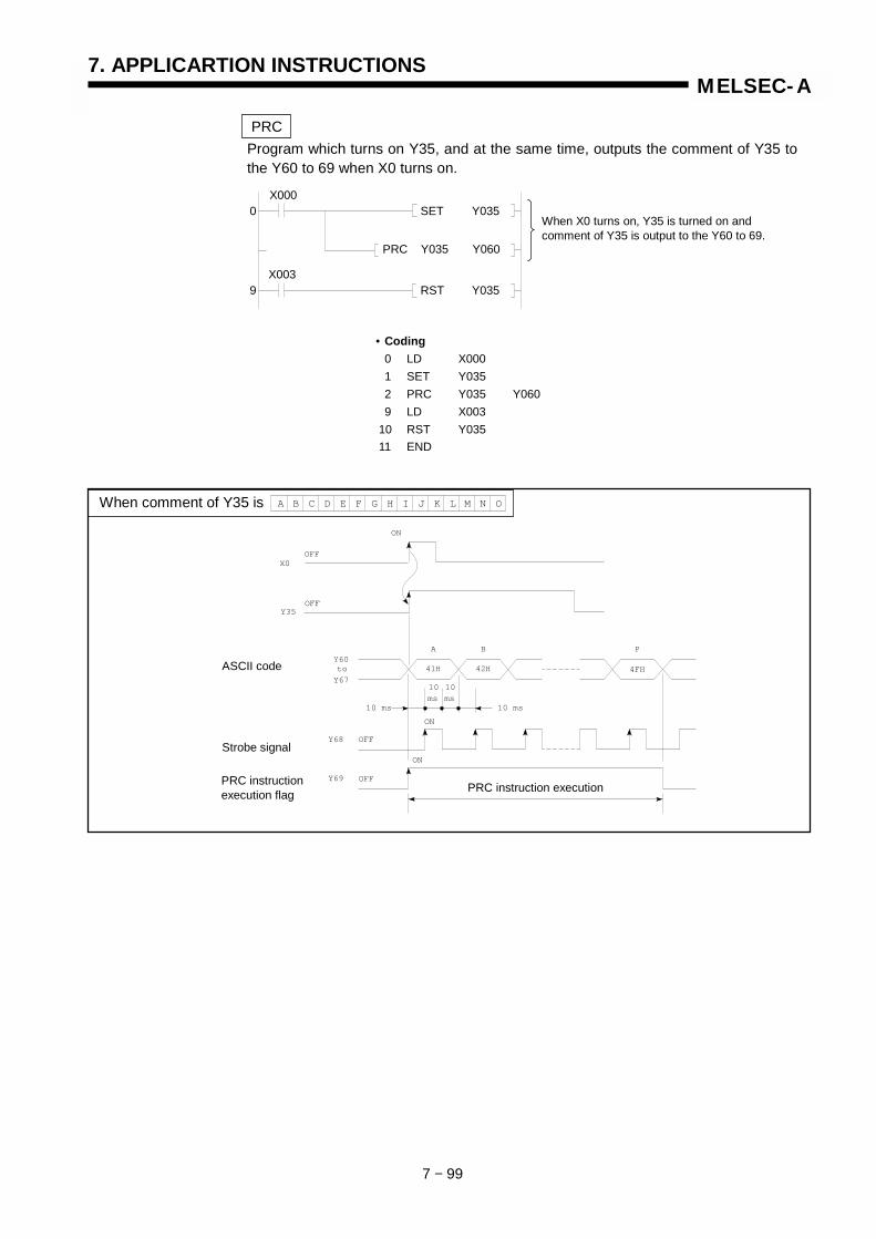
7. APPLICARTION INSTRUCTIONS
7 − 99
MELSEC-A
PRCProgram which turns on Y35, and at the same time, outputs the comment of Y35 tothe Y60 to 69 when X0 turns on.
When comment of Y35 is
• Coding0 LD X0001 SET Y0352 PRC Y035 Y0609 LD X003
10 RST Y03511 END
A B C D E F G H I J K L M N O
ASCII codeY60
10ms
10ms
10 ms
41H 42H 4FH
A B P
10 ms
OFF
ON
OFF
OFF
ON
to
Y35
X0
OFF
ON
Y67
Y68
Y69
Strobe signal
PRC instructionexecution flag PRC instruction execution
When X0 turns on, Y35 is turned on andcomment of Y35 is output to the Y60 to 69.
X000
X003
SET Y035
PRC Y035 Y060
RST Y035
0
9

7. APPLICATION INSTRUCTIONS
7 − 100
MELSEC-A
7.9.2 ASCII code comment display instruc-tions (LED, LEDC)
Available Device
Bit device Word (16-bit) device Constant Pointer Level Car
ryfla
g
Erro
rfla
g
X Y M L S B F T C D W R A0 A1 Z V K H P I N
Digi
t spe
cific
atio
n
Inde
x
M9012 (M9010, M9011)
LED O O O O O
LEDC(S)
O O O O O O O O O O O O O OO O
1: For the number of steps when AnA, A2AS, AnU, QCPU-A (A Mode) and A2USH board is used, refer to Section 3.8.1.
Functions LED(1) Displays the ASCII data (16 characters) stored at eight points, which begin with
the device specified at (S), at the LED indicator on the front face of CPU.
(2) When the ASCII data is not stored at the eight points which begin with thedevice specified at (S).1) T, C, D, W: Blank2) R: What will be displayed is unknown.
(Blank when the file register (R) has been cleared.)
(3) For ASCII characters which can be displayed, refer to (3) in the section of the LEDC instruction.
(4) For the conversion of alphanumeric characters into ASCII data in a sequenceprogram, use the ASC instruction.
AnSAnN
AnSHAn A1FX A3H
A3M A3V AnA
AnU, A2ASA2USH-S1
A2USH boardQCPU-A(A Mode)
A0J2H A2CA52G A73 A3N
boardApplicableCPU
X O O X X O O
Remark *1: A3N only. *3: A3A only.*2: A3 only. *4: A3U and A4U only.
*1 *2 *3 *4
LED, LEDC
Indicates the instruction symbol.Display command
(S) LED Head number of device whichstores displayed data
(S)LEDC Device number of which com-
ment will be displayed
Setting data
Display data
LED indicator on front face of CPU
ASCII characterStored ASCII data (hexadecimal)
41 (A)
43 (C)
45 (E)
47 (G)
4B (K)
4D (M)
4F (O)
49 (I)
42 (B)
44 (D)
46 (F)
48 (H)
4C (L)
4E (N)
50 (P)
4A (J)
A B C D E F G H I J K L M N O P
(S)+7
(S)+6
(S)+5
(S)+4
(S)+3
(S)+2
(S)+1
(S)
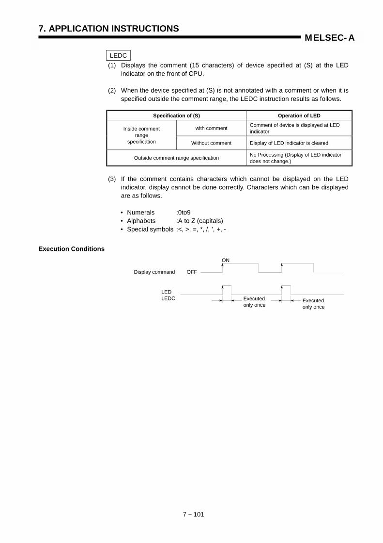
7. APPLICATION INSTRUCTIONS
7 − 101
MELSEC-A
LEDC(1) Displays the comment (15 characters) of device specified at (S) at the LED
indicator on the front of CPU.
(2) When the device specified at (S) is not annotated with a comment or when it isspecified outside the comment range, the LEDC instruction results as follows.
Specification of (S) Operation of LED
with comment Comment of device is displayed at LEDindicatorInside comment
rangespecification Without comment Display of LED indicator is cleared.
Outside comment range specification No Processing (Display of LED indicatordoes not change.)
(3) If the comment contains characters which cannot be displayed on the LEDindicator, display cannot be done correctly. Characters which can be displayedare as follows.
• Numerals :0to9• Alphabets :A to Z (capitals)• Special symbols :<, >, =, *, /, ’, +, -
Execution Conditions
Display command OFF
LEDLEDC Executed
only once
ON
Executedonly once
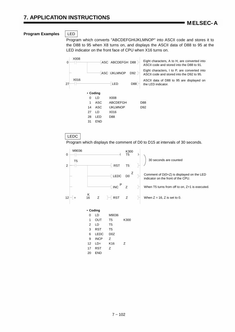
7. APPLICATION INSTRUCTIONS
7 − 102
MELSEC-A
Program Examples LEDProgram which converts "ABCDEFGHIJKLMNOP" into ASCII code and stores it tothe D88 to 95 when X8 turns on, and displays the ASCII data of D88 to 95 at theLED indicator on the front face of CPU when X16 turns on.
LEDCProgram which displays the comment of D0 to D15 at intervals of 30 seconds.
• Coding0 LD X0081 ASC ABCDEFGH D88
14 ASC IJKLMNOP D9227 LD X01628 LED D8831 END
• Coding0 LD M90361 OUT T5 K3002 LD T53 RST T56 LEDC D0Z9 INCP Z
12 LD= K16 Z17 RST Z20 END
( )
30 seconds are counted
Comment of D(0+Z) is displayed on the LEDindicator on the front of the CPU.
When T5 turns from off to on, Z+1 is executed.
When Z = 16, Z is set to 0.
0 T5
2 RST T5
12 = 16 Z RST Z
M9036 K300
K
LEDC D0
INC ZP
Z
T5
Eight characters, A to H, are converted intoASCII code and stored into the D88 to 91.
Eight characters, I to P, are converted intoASCII code and stored into the D92 to 95.
ASCII data of D88 to 95 are displayed onthe LED indicator.
ASC IJKLMNOP D92
X008
X016
ASC ABCDEFGH D88
LED D88
0
27

MEMO

7. APPLICATION INSTRUCTIONS
7 − 103
MELSEC-A
7.9.3 Character display instructions(LEDA, LEDB)
The LEDA/LEDB instructions are used as the starting command for the dedicatedinstructions for the AnA, A2AS, AnSH, AnU, QCPU-A (A Mode) and A2USH board.For details, refer to the AnSHCPU/AnACPU/AnUCPU Programming Manual(Dedicated Instructions).
Available Device
Bit device Word (16-bit) device Constant Pointer Level Car
ryfla
g
Erro
rfla
g
X Y M L S B F T C D W R A0 A1 Z V K H P I N
Digi
t spe
cific
atio
n
Inde
x
M9012 (M9010, M9011)
Functions (1) Displays the ASCII characters spexified by LEDA and LEDB at the LED indicator on the CPU front.
(2) The displays of LEDA and LEDB are as shown below.
(3) The following items can be displayed by the display instructions on the LEDdisplay on the front panel of the CPU module.
• Numeral : 0 to 9• Alphabet : A to Z (Capitals)• Special symbol: <, >, =,*, /, ’, +, -
Execution Conditions
AnSAnN
AnSHAn A1FX A3H
A3M A3V AnA
AnU, A2ASA2USH-S1
A2USH boardQCPU-A(A Mode)
A0J2H A2CA52G A73 A3N
boardApplicableCPU
X O O X X X X O O
Remark *1: A3N only.*2: A3 only.
Display command
LEDA
LEDB
ASCII characters(first 8 characters)
ASCII characters(last 8 characters)
Specification of 16 charactersdisplayed at LED indicator
A B C D E F G H I J K L M N O P
LEDA LEDB
LED indicator at CPU front (16 characters)
Specification of firsthalf 8 characters
Specification of lasthalf 8 characters
*2*1
Display command OFF
ON
Executedonly once
LEDALEDB Executed
only once

7. APPLICATION INSTRUCTIONS
7 − 104
MELSEC-A
Program Examples LEDA , LEDBProgram which displays "ABCDEFGHIJKLMNOP" at the LED indicator on the CPUfront when XC turns on.
REMARKS
The second eight of the 16 characters displayed by the LED instruction will disappear if the firsteight are rewritten by the LEDA instruction.The first eight characters will disappear if the second eight are rewritten by the LED instruction.
• Coding0 LD X00C1 LEDA ABCDEFGH
14 LEDB IJKLMNOP27 END
First half 8 characters are specified.
Last half 8 characters are specified.
0X00C
LEDA ABCDEFGH
LEDB IJKLMNOP

7. APPLICATION INSTRUCTIONS
7 − 105
MELSEC-A
7.9.4 Annunciator reset instruction(LEDR)
In the case of the CPU modules which have an LED indicator on its front side,pressing the "INDICATOR RESET" switch executes the processing same as thatcalled by the LEDR instruction.
Available Device
Bit device Word (16-bit) device Constant Pointer Level Car
ryfla
g
Erro
rfla
g
X Y M L S B F T C D W R A0 A1 Z V K H P I N
Digi
t spe
cific
atio
n
Num
ber o
f ste
ps
M9012 (M9010, M9011)
1
Reses of the CPU annunciator display and the self-diagnosis error display.
• When there is a self-diagnosis error though the CPU can continue the operation.Reset the "ERROR" LED or error display on the front of the CPU when the self-diagnosis error is displayed.The contents in M9008 and D9008 are not reset, so they should be reset by usingthe user’s program.At this time, the annunciator is not reset.
• When the annunciator is ON
Functions CPU modules which do not have an LED indicator on the front panelPerforms the following actions:(1) Flickers and then turns off the "ERROR" LED.(2) Resets the annunciator (F) stored in D9009.(3) Resets D9009 and 9125 and shifts the F numbers of D9126 to 9131 to be
processed.(4) Transfers the F number, which has been newly stored in D9125, to D9009.(5) Reduces -1 from the data of D9124. However, when D9124 is 0, the data
remains 0.
ApplicableCPU All CPUs
Reset instruction
LEDR

7. APPLICATION INSTRUCTIONS
7 − 106
MELSEC-A
CPU modules which have an LED indicator on the front panelPerforms the following actions:(1) Resets the F number displayed at the CPU front.(2) Resets the annunciator (F) stored in D9009.(3) Resets D9009 and 9125 and shifts the F numbers of D9126 to 9132 to be
processed.(4) Transfers the F number, which has been newly stored in D9125, to D9009.(5) Reduces -1 from the data of D9124. However, when D9124 is 0, the data
remains 0.(6) Displays the F number stored in D9009 at the LED indicator. (When D9124 is 0,
the F number is not displayed.)
200
5
200
99
5
255
0
0
D9009
D9124
D9125
D9126
D9127
D9128
D9131
D9132
99
4
99
5
255
0
0
0
D9009
D9124
D9125
D9126
D9127
D9130
D9131
D9132
D9129
D9130
83
0
D9128
D9129
83
0
Number of enteredF numbers
F number storage area
(annunciaor accumulator)
Beforeexecution
Afterexecution
-1 isreduced
200
1
200
0
0
0
0
0
D9009
D9124
D9125
D9126
D9127
D9128
D9131
D9132
0
0
0
0
0
0
0
0
D9009
D9124
D9125
D9126
D9127
D9130
D9131
D9132
D9129
D9130
0
0
D9128
D9129
0
0
Since D9124 is 0, Fnumber is not displayedat LED indicator.
Number of entered Fnumbers (annunciatoraccumulator)
Beforeexecution
Afterexecution
-1 isreduced
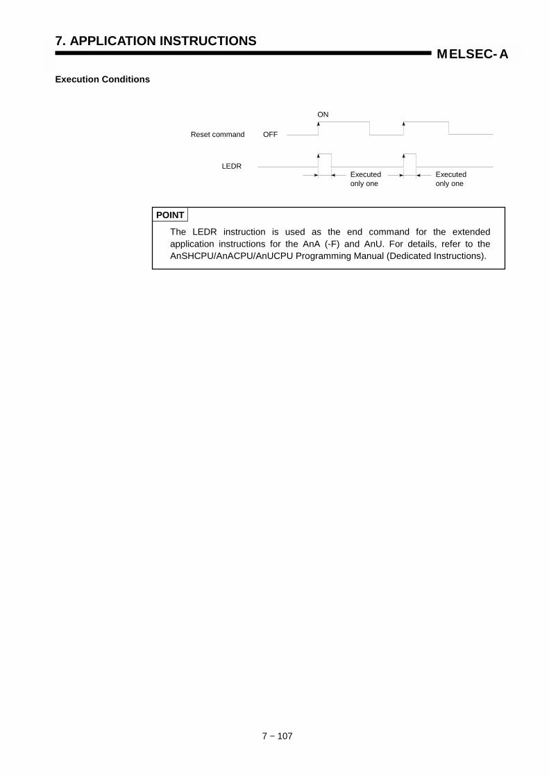
7. APPLICATION INSTRUCTIONS
7 − 107
MELSEC-A
Execution Conditions
POINT
The LEDR instruction is used as the end command for the extendedapplication instructions for the AnA (-F) and AnU. For details, refer to theAnSHCPU/AnACPU/AnUCPU Programming Manual (Dedicated Instructions).
Reset command OFF
ON
LEDRExecutedonly one
Executedonly one

7. APPLICATION INSTRUCTIONS
7 − 108
MELSEC-A
7.10 Other Instructions
Instructions which perform operations such as the reset of WDT, the failure check,and the set and reset of carry flag.
Classification Instruction Symbol Ref. Page
WDT reset WDT 7-109
Failure check CHK 7-111
Set SLT 7-117Status latch
Reset SLTR 7-117
Set STRA 7-119Sampling trace
Reset STRAR 7-119
Set STC 7-121Carry
Reset CLC 7-121
Timing clock DUTY 7-123
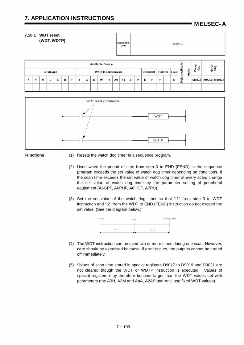
7. APPLICATION INSTRUCTIONS
7 − 109
MELSEC-A
7.10.1 WDT reset(WDT, WDTP)
Available Device
Bit device Word (16-bit) device Constant Pointer Level Car
ryfla
g
Erro
rfla
g
X Y M L S B F T C D W R A0 A1 Z V K H P I N
Digi
t spe
cific
atio
n
Inde
x
M9012 (M9010, M9011)
Functions (1) Resets the watch dog timer in a sequence program.
(2) Used when the period of time from step 0 to END (FEND) in the sequenceprogram exceeds the set value of watch dog timer depending on conditions. Ifthe scan time exceeds the set value of watch dog timer at every scan, changethe set value of watch dog timer by the parameter setting of peripheralequipment (A6GPP, A6PHP, A6HGP, A7PU).
(3) Set the set value of the watch dog timer so that "t1" from step 0 to WDTinstruction and "t2" from the WDT to END (FEND) instruction do not exceed theset value. (See the diagram below.)
(4) The WDT instruction can be used two or more times during one scan. However,care should be exercised because, if error occurs, the outputs cannot be turnedoff immediately.
(5) Values of scan time stored in special registers D9017 to D9019 and D9021 arenot cleared though the WDT or WDTP instruction is executed. Values ofspecial registers may therefore become larger than the WDT values set withparameters (the A3H, A3M and AnA, A2AS and AnU use fixed WDT values).
ApplicableCPU All CPUs
WDT
WDTP
WDT reset commands
Step 0 END(FEND)WDT
t 1 t 2

7. APPLICATION INSTRUCTIONS
7 − 110
MELSEC-A
Execution Conditions
Program Example WDTProgram used when the setting of watch dog timer is 200 ms and the period of timefrom 0 to END (FEDN) instruction is 300 ms depending on the execution conditionsof program.
OFF
ON
Executedper scan
Executedper scan
Executedonly once
Executedonly once
WDT
WDTP
WDT reset command
Program of300 ms
Program of150 ms
Program of150 ms
WDT
END END
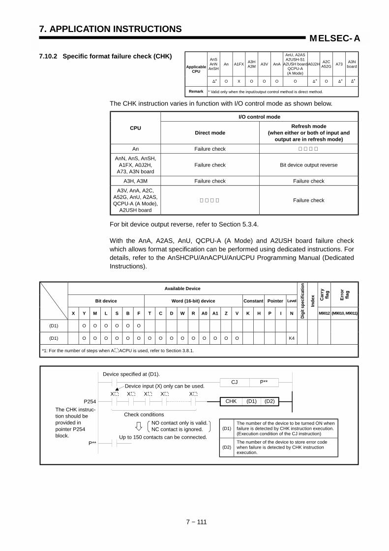
7. APPLICATION INSTRUCTIONS
7 − 111
MELSEC-A
7.10.2 Specific format failure check (CHK)
The CHK instruction varies in function with I/O control mode as shown below.
I/O control mode
CPUDirect mode
Refresh mode(when either or both of input and
output are in refresh mode)
An Failure check
AnN, AnS, AnSH,A1FX, A0J2H,
A73, A3N boardFailure check Bit device output reverse
A3H, A3M Failure check Failure check
A3V, AnA, A2C,A52G, AnU, A2AS,QCPU-A (A Mode),
A2USH board
Failure check
For bit device output reverse, refer to Section 5.3.4.
With the AnA, A2AS, AnU, QCPU-A (A Mode) and A2USH board failure checkwhich allows format specification can be performed using dedicated instructions. Fordetails, refer to the AnSHCPU/AnACPU/AnUCPU Programming Manual (DedicatedInstructions).
Available Device
Bit device Word (16-bit) device Constant Pointer Level Car
ryfla
g
Erro
rfla
g
X Y M L S B F T C D W R A0 A1 Z V K H P I N
Digi
t spe
cific
atio
n
Inde
xM9012 (M9010, M9011)
(D1) O O O O O O
(D1) O O O O O O O O O O O O O O O K4
*1: For the number of steps when A ACPU is used, refer to Section 3.8.1.
AnSAnN
AnSHAn A1FX A3H
A3M A3V AnA
AnU, A2ASA2USH-S1
A2USH boardQCPU-A(A Mode)
A0J2H A2CA52G A73 A3N
boardApplicableCPU
O X O O O O O
Remark * Valid only when the input/output control method is direct method.
Device specified at (D1).
Device input (X) only can be used.
Up to 150 contacts can be connected.
NO contact only is valid.NC contact is ignored.
Check conditionsThe CHK instruc-tion should beprovided inpointer P254block.
CJ P**
CHK (D1) (D2)X X X X X
P254
P**
(D1)The number of the device to be turned ON whenfailure is detected by CHK instruction execution.(Execution condition of the CJ instruction)
(D2)The number of the device to store error codewhen failure is detected by CHK instructionexecution.
* * * *
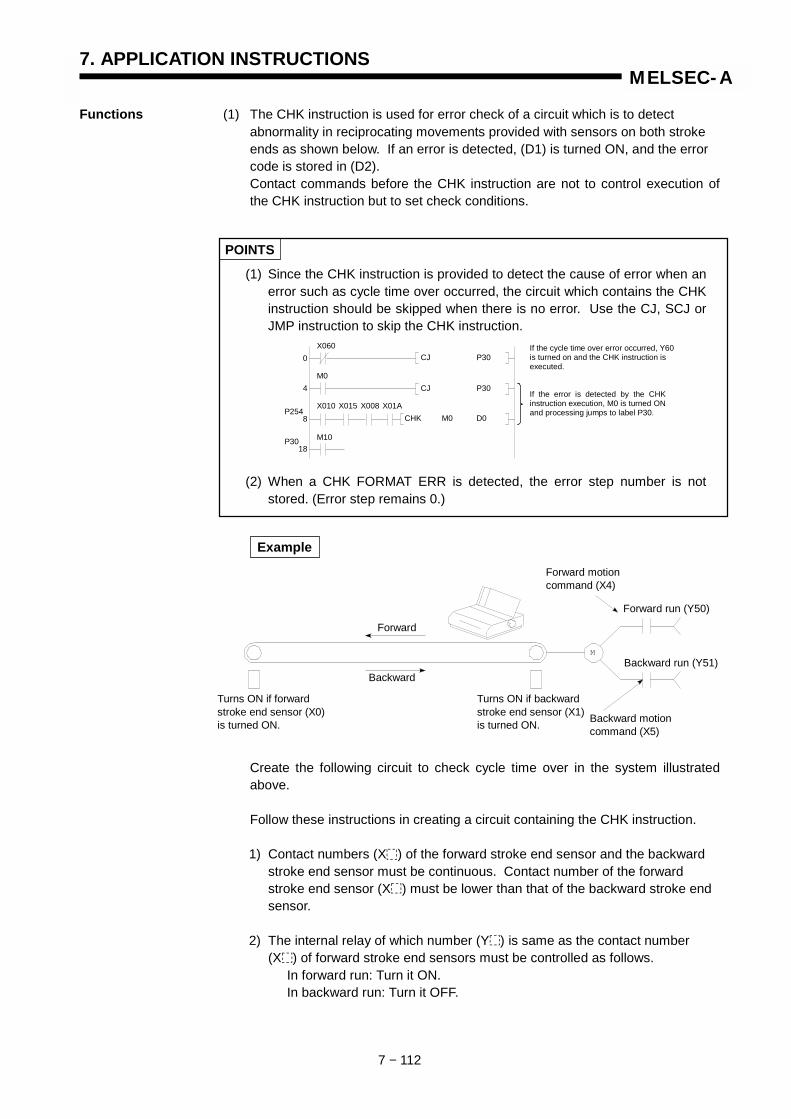
7. APPLICATION INSTRUCTIONS
7 − 112
MELSEC-A
Functions (1) The CHK instruction is used for error check of a circuit which is to detectabnormality in reciprocating movements provided with sensors on both stroke ends as shown below. If an error is detected, (D1) is turned ON, and the error code is stored in (D2).Contact commands before the CHK instruction are not to control execution ofthe CHK instruction but to set check conditions.
POINTS
(1) Since the CHK instruction is provided to detect the cause of error when anerror such as cycle time over occurred, the circuit which contains the CHKinstruction should be skipped when there is no error. Use the CJ, SCJ orJMP instruction to skip the CHK instruction.
(2) When a CHK FORMAT ERR is detected, the error step number is notstored. (Error step remains 0.)
Example
Create the following circuit to check cycle time over in the system illustratedabove.
Follow these instructions in creating a circuit containing the CHK instruction.
1) Contact numbers (X ) of the forward stroke end sensor and the backwardstroke end sensor must be continuous. Contact number of the forwardstroke end sensor (X ) must be lower than that of the backward stroke endsensor.
2) The internal relay of which number (Y ) is same as the contact number(X ) of forward stroke end sensors must be controlled as follows.
In forward run: Turn it ON.In backward run: Turn it OFF.
X060
M0
X010
M10
X015 X008 X01A
0
4
8
18
P254
P30
CJ P30
CJ P30
CHK M0 D0
If the cycle time over error occurred, Y60is turned on and the CHK instruction isexecuted.
If the error is detected by the CHKinstruction execution, M0 is turned ONand processing jumps to label P30.
M
Forward motioncommand (X4)
Forward run (Y50)
Backward run (Y51)
Backward motioncommand (X5)
Turns ON if backwardstroke end sensor (X1)is turned ON.
Turns ON if forwardstroke end sensor (X0)is turned ON.
Forward
Backward

7. APPLICATION INSTRUCTIONS
7 − 113
MELSEC-A
(2) The CHK instruction executes processing equivalent to the circuit shown belowwith one specified contact.
POINT
The CHK instruction performs error check following the circuit patternillustrated above. The circuit pattern cannot be changed.
M0
X Y
XX
CJ P0
CHK M0 D0
Max. 150 contact points
(Both of the forward stroke end and backwardstroke end sensors are actuated in forward run.)
Condition 1
Condition 2
Condition 3
Condition 4
Condition 5
Condition 6
X +1SET M0
MOV D0Error code 1(Both of the forward stroke end and backwardstroke end sensors are actuated in forward run.)X YX +1
SET M0
MOV D0Error code 2(Backward run when the forward stroke endsensor is actuated.)X Y
SET M0
MOV D0Error code 3(Forward run when the backward stroke endsensor is actuated.)Y X +1
SET M0
MOV D0Error code 4(Forward run when the backward stroke endsensor is not actuated.)Y X +1
SET M0
MOV D0Error code 5(Backward run when the forward stroke endsensor is not actuated.)X Y
SET M0
MOV D0Error code 6
Example Processing is performed asX is X0, X +1 is X1 and Y is Y0.
P254
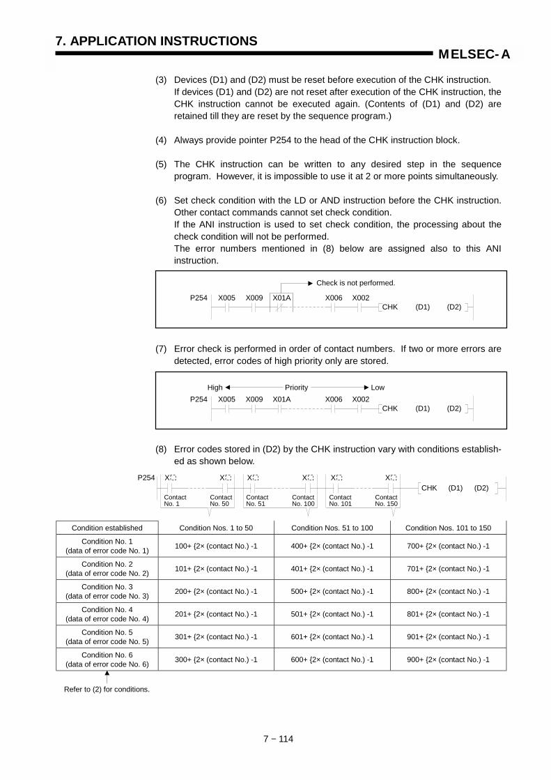
7. APPLICATION INSTRUCTIONS
7 − 114
MELSEC-A
(3) Devices (D1) and (D2) must be reset before execution of the CHK instruction.If devices (D1) and (D2) are not reset after execution of the CHK instruction, theCHK instruction cannot be executed again. (Contents of (D1) and (D2) areretained till they are reset by the sequence program.)
(4) Always provide pointer P254 to the head of the CHK instruction block.
(5) The CHK instruction can be written to any desired step in the sequenceprogram. However, it is impossible to use it at 2 or more points simultaneously.
(6) Set check condition with the LD or AND instruction before the CHK instruction.Other contact commands cannot set check condition.If the ANI instruction is used to set check condition, the processing about thecheck condition will not be performed.The error numbers mentioned in (8) below are assigned also to this ANIinstruction.
(7) Error check is performed in order of contact numbers. If two or more errors aredetected, error codes of high priority only are stored.
(8) Error codes stored in (D2) by the CHK instruction vary with conditions establish-ed as shown below.
Condition established Condition Nos. 1 to 50 Condition Nos. 51 to 100 Condition Nos. 101 to 150
Condition No. 1(data of error code No. 1) 100+ {2× (contact No.) -1 400+ {2× (contact No.) -1 700+ {2× (contact No.) -1
Condition No. 2(data of error code No. 2) 101+ {2× (contact No.) -1 401+ {2× (contact No.) -1 701+ {2× (contact No.) -1
Condition No. 3(data of error code No. 3) 200+ {2× (contact No.) -1 500+ {2× (contact No.) -1 800+ {2× (contact No.) -1
Condition No. 4(data of error code No. 4) 201+ {2× (contact No.) -1 501+ {2× (contact No.) -1 801+ {2× (contact No.) -1
Condition No. 5(data of error code No. 5) 301+ {2× (contact No.) -1 601+ {2× (contact No.) -1 901+ {2× (contact No.) -1
Condition No. 6(data of error code No. 6) 300+ {2× (contact No.) -1 600+ {2× (contact No.) -1 900+ {2× (contact No.) -1
P254 X005 X009 X01A X006 X002CHK (D1) (D2)
Check is not performed.
P254 X005 X009 X01A X006 X002CHK (D1) (D2)
PriorityHigh Low
Refer to (2) for conditions.
X X X X X X
ContactNo. 1
ContactNo. 50
ContactNo. 51
ContactNo. 100
ContactNo. 101
ContactNo. 150
CHK (D1) (D2)P254

7. APPLICATION INSTRUCTIONS
7 − 115
MELSEC-A
REMARK
Error code numbers displayed after the CHK instruction execution indicate kind of the erroroccurred. Prepare a troubleshooting table corresponding to the system for quick remedies.
List of Error Code Numbers (Error codes are stored by BCD.)
Error Code Numbers for the CHK Instruction
Execution The CHK instruction is executed every scan regardless of ON/OFF status of checkConditions condition contact points.
POINT
The CHK instruction cannot be written and modified during PC CPU RUN.
Error codeNo.
Cause Corrective action
301Conveyor 1: Backward run occurredwhen the forward stroke end sensorwas not actuated.
• Check limit switch X1.• Check the conveyor.
n=1
X10 X16
n=2
X52
n=50
X54
n=51
X74
n=100
X7A
n=101
XA2
n=149
XA4
n=150
CHK (D1) (D2)
*1High Priority Low
100 102 198 400 498 700 796 798
101 103 199 401 499 701 797 799
200 202 298 500 598 800 896 898
201 203 299 501 599 801 897 899
301 303 399 601 699 901 997 999
300 302 398 600 698 900 996 998
X10 X11 Y10
X10 X11 Y10
Y10 X10
Y10 X11
Y10 X11
Y10 X10
X16 X17 Y16
X16 X17 Y16
Y16 X16
Y16 X17
Y16 X17
Y16 X16
X52 X53 Y52
X52 X53 Y52
Y52 X52
Y52 X53
Y52 X53
Y52 X52
X54 X55 Y54
X54 X55 Y54
Y54 X54
Y54 X54
Y54 X55
Y54 X54
X74 X75 Y74
Y74 X74
Y74 X75
Y74 X75
Y74 X74
X7A X7B Y7A
X7A X7B Y7A
Y7A X7A
X7A X7B
X7A X7B
Y7A X7A
XA2 XA3 YA2
XA2 XA3 YA2
YA2 XA2
YA4 XA5 YA4
YA4 XA5 TA4
YA4 XA4
X74 X75 Y74
YA2 XA3
YA2 XA3
YA2 XA2
YA4 YA5
YA4 XA5
YA4 XA4
Priority
Low
High
Error code numbers
Order of
contact points
Order ofcontact points
High Priority Low
Hig
hPr
iorit
yLo
w
Erro
r cod
e nu
mbe
rs

7. APPLICATION INSTRUCTIONS
7 − 116
MELSEC-A
Operation Errors In the following cases, operation error occurs and the PC CPU stops operation.
• When parallel circuits are provided:
• When NOP is contained:
• When label P254 is not contained:
• When the number of contact points exceeds 150:
• When there is no circuit block of CJ:
POINT
Operation error occurs when the NOP instruction is in the format determinedby the CHK instruction.Check the NOP instruction in list mode because it is not displayed in theladder mode of GPP.
Bit device specified at (D1).
LabelP254
CJ P∗∗
CHK (D1) (D2)
CJ P∗∗
CHK (D1) (D2)P254
Eliminate parallel contacts.
Eliminate parallel contactsin the circuit block of CJ.
CJ P∗∗
CHK (D1) (D2)P254
Delete NOP.(LDI and ANI substitute NOP.)NOP
Not displayed in ladder mode.
CJ P∗∗
CHK (D1) (D2) Insert label P254.
CJ P∗∗
CHK (D1) (D2) Reduce contact points below 150.P254
151 or more contact points
CHK (D1) (D2) Add a circuit block of CJ.P254

7. APPLICATION INSTRUCTIONS
7 − 117
MELSEC-A
7.10.3 Status latch set, reset(STL, SLTR)
Available Device
Bit device Word (16-bit) device Constant Pointer Level Car
ryfla
g
Erro
rfla
g
X Y M L S B F T C D W R A0 A1 Z V K H P I N
Digi
t spe
cific
atio
n
Inde
x
M9012 (M9010, M9011)
Functions SLT(1) When executed, the SLT instruction stores the contents of data memories and
file registers set by the parameter setting of peripheral unit A6GPP, A6PHP,A6HGP into the memory for status latch in the user memory area.
(2) Stausu latch is allowed for the following devices.Data memory: ON/OFF displays of X, Y, M, B, and F
Present valuses of T and CContents of D, W, A0, A1, Z and V
Contents of file registers
(3) When the SLT instruction is executed only once.
(4) The result of status latch can be monitored by the A6GPP, A6PHP, A6HGP.
SLTR(1) A reset instruction of SLT instruction.
(2) By executing the SLTR instruction, the SLT instruction is enabled again.
Execution Conditions
AnSAnN
AnSHAn A1FX A3H
A3M A3V AnA
AnU, A2ASA2USH-S1
A2USH boardQCPU-A(A Mode)
A0J2H A2CA52G A73 A3N
boardApplicableCPU
O O O O O O O O O
Remark *1: Unusable with A1N.*2: Unusable with A1.
SLT
SLTR
Execution ofstatus latch
Reset of statuslatch
Status latch command
Reset command
OFF
ON
Executedonly once
Status latch command
OFF
Executed only once
Reset command
SLT
SLTR
ON
Executed only once
*1 *2

7. APPLICATION INSTRUCTIONS
7 − 118
MELSEC-A
POINT
When the status latch (SLT) instruction is executed, the scan time of program-mable controller CPU increases as shown in the following table.
Latch of OnlyDevice Memory
Latch of Both DeviceMemory and File Register
A2(-S1), A2CA0J2H, A52G 11 ms 21 ms
A3 11 ms 31 msA2N(-S1), A1S(-S1)A1SJ(-S3), A2S)-S1) 8.5 ms 25 ms
A3N, A73, A3N board 8.5 ms 37 msA3H, A3M 4.1 ms 10.4 ms
A2A(-S1), A2UA2AS(-S1/S30/S60) 2.9 ms 12.9 ms
A3A, A3U, A4U, A3A 2.2 ms 9.7 msA2USH-S1,
A2USH board1.3 ms 4.5 ms
A1SH, A1SJH 1.5 ms 3.8 msA2SH(-S1) 1.4 ms 3.0 ms
A1FX 1.4 ms 3.0 msQ02 4.6 ms 6.1 ms
Q02H, Q06H 1.7 ms 2.3 ms
Set the watch dog timer of programmable controller CPU after considering theabove increase in scan time.
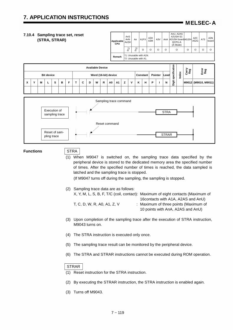
7. APPLICATION INSTRUCTIONS
7 − 119
MELSEC-A
7.10.4 Sampling trace set, reset(STRA, STRAR)
Available Device
Bit device Word (16-bit) device Constant Pointer Level Car
ryfla
g
Erro
rfla
g
X Y M L S B F T C D W R A0 A1 Z V K H P I N
Digi
t spe
cific
atio
n
Inde
x
M9012 (M9010, M9011)
Functions STRA(1) When M9047 is switched on, the sampling trace data specified by the
peripheral device is stored to the dedicated memory area the specified numberof times. After the specified number of times is reached, the data sampled islatched and the sampling trace is stopped.(If M9047 turns off during the sampling, the sampling is stopped.
(2) Sampling trace data are as follows:X, Y, M, L, S, B, F, T/C (coil, contact): Maximum of eight contacts (Maximum of
16contacts with A1A, A2AS and AnU)T, C, D, W, R, A0, A1, Z, V : Maximum of three points (Maximum of
10 points with AnA, A2AS and AnU)
(3) Upon completion of the sampling trace after the execution of STRA instruction,M9043 turns on.
(4) The STRA instruction is executed only once.
(5) The sampling trace result can be monitored by the peripheral device.
(6) The STRA and STRAR instructions cannot be executed during ROM operation.
STRAR(1) Reset instruction for the STRA instruction.
(2) By executing the STRAR instruction, the STRA instruction is enabled again.
(3) Turns off M9043.
AnSAnN
AnSHAn A1FX A3H
A3M A3V AnA
AnU, A2ASA2USH-S1
A2USH boardQCPU-A(A Mode)
A0J2H A2CA52G A73 A3N
boardApplicableCPU
O O O O O O O O O
Remark *1: Unusable with A1N.*2: Unusable with A1.
STRA
STRAR
Execution ofsampling trace
Reset of sam-pling trace
Sampling trace command
Reset command
*1 *2

7. APPLICATION INSTRUCTIONS
7 − 120
MELSEC-A
Excecution ConditionsON
Executed only once
Sampling trace command
OFFON
Executed only once
Reset command
STRA
STRAR
OFF
Executed only once
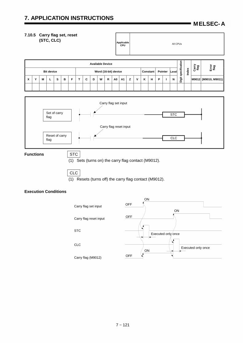
7. APPLICATION INSTRUCTIONS
7 − 121
MELSEC-A
7.10.5 Carry flag set, reset(STC, CLC)
Available Device
Bit device Word (16-bit) device Constant Pointer Level Car
ryfla
g
Erro
rfla
g
X Y M L S B F T C D W R A0 A1 Z V K H P I N
Digi
t spe
cific
atio
n
Inde
x
M9012 (M9010, M9011)
Functions STC(1) Sets (turns on) the carry flag contact (M9012).
CLC(1) Resets (turns off) the carry flag contact (M9012).
Execution Conditions
ApplicableCPU All CPUs
STC
CLC
Set of carryflag
Reset of carryflag
Carry flag set input
Carry flag reset input
OFFON
Executed only once
Carry flag set input
OFF
ON
Executed only once
Carry flag reset input
STC
CLC
OFFON
Carry flag (M9012)

7. APPLICATION INSTRUCTIONS
7 − 122
MELSEC-A
Program Example STC , CLCProgram which performs addition of the BCD data of X0 to F and the BCD data ofD0 when M0 turns on, and turns on the carry flag (M9012) when the result is morethan 9999, and turns off the carry flag when the result is 9999 or less.
( )
M00
P K4B+ X000 D0 D1
K4> X000 D1
BCD data of X0 to F and that of D0 are addedand the result is stored into D1.
When (addend) > (addition result) or (augend) >(addition result), M1 is turned on.
•••• Coding0 LD M01 B+P K4X000 D0 D1
10 LD> K4X000 D115 OR> D0 D120 OUT M121 LD M122 STC23 LDI M124 CLC25 END
When M1 turns on, carry flag is turned on.
M1
> D0 D1
STC
CLC
10
21
23
M1
M1When M1 is off, carry flag is off.

7. APPLICATION INSTRUCTIONS
7 − 123
MELSEC-A
7.10.6 Pulse regeneration instruction(DUTY)
Available Device
Bit device Word (16-bit) device Constant Pointer Level Car
ryfla
g
Erro
rfla
g
X Y M L S B F T C D W R A0 A1 Z V K H P I N
Digi
t spe
cific
atio
n
Inde
x
M9012 (M9010, M9011)
n1 O O
n2 O O
(D) O
O
*1: Index qualification can be used with AnA and AnU only.
Functions (1) Sets the timing clock for user (M9020 to 9024) specified at (D) to ON at thescan count specified at "n1" and to OFF at the scan count specified at "n2".
(2) At the initial status (when the timing pulse input is off), the timing pulse is off.
(3) When "n1" and "n2" are set to 0, the timing pulse is as described below:"n1" = 0: The timing pulse remains off."n1" > 0, "n2" = 0: The timing pulse remains on.
Execution Conditions
Operation Error In the following case, operation error occurs and the error flag turns on.• The setting of D is other than M9020 to 9024.
ApplicableCPU All CPUs
*1
DUTY
Start input
n1 n2 (D)
n1 Number of scans duringwhich timing pulse is on
n2 Number of scans duringwhich timing pulse is off
(D) Timing clocks for user(M9020 to 4)
Setting data
OFF
ON
Executed only once
Start input
OFF
ON
DUTY
Timing pulsen1 scans n2 scans
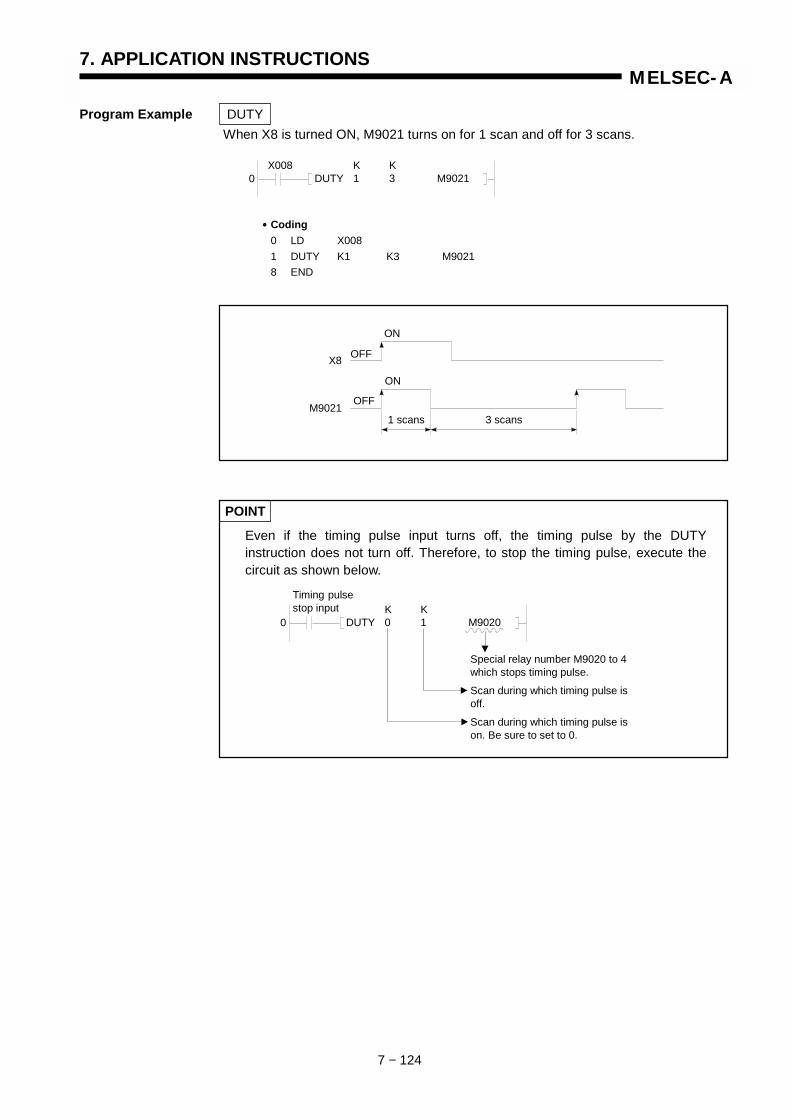
7. APPLICATION INSTRUCTIONS
7 − 124
MELSEC-A
Program Example DUTYWhen X8 is turned ON, M9021 turns on for 1 scan and off for 3 scans.
POINT
Even if the timing pulse input turns off, the timing pulse by the DUTYinstruction does not turn off. Therefore, to stop the timing pulse, execute thecircuit as shown below.
0X008 K K
DUTY 1 3 M9021
•••• Coding0 LD X0081 DUTY K1 K3 M90218 END
OFF
ON
X8
OFF
ON
M90211 scans 3 scans
0
Timing pulsestop input K K
DUTY 0 1 M9020
Special relay number M9020 to 4which stops timing pulse.
Scan during which timing pulse isoff.
Scan during which timing pulse ison. Be sure to set to 0.
7. APPLICATION INSTRUCTIONS
7 − 125
MELSEC-A
7.11 Servo Program Instructions
Servo program instructions are used with the A73 for start request and data changeof servo programs.There are 2 servo program instructions as shown below.
Name Symbol Refer to Name Symbol Refer to
Start request DSFRP 7-125 Data change DSFLP 7-130
For control parameters, positioning devices, positioning procedures and preparationof servo programs required for positioning control with the A73CPU, refer to theA73CPU Reference Manual.
POINT
Servo program instructions are dedicated to the A73CPU. The DSFRP andDSFLP instructions used with other types of CPUs perform 1-word shiftprocessing of n word data.

MEMO

7. APPLICATION INSTRUCTIONS
7 − 126
MELSEC-A
7.11.1 Servo program start (DSFRP)
Available Device
Bit device Word (16-bit) device Constant Pointer Level Car
ryfla
g
Erro
rfla
g
X Y M L S B F T C D W R A0 A1 Z V K H P I N
Digi
t spe
cific
atio
n
Inde
x
M9012 (M9010, M9011)
(D) O
n O OO
Functions (1) Servo program start request is executed after the DSFRP instruction execution command was turned ON, and the start enable flag (M200n) which correspondsto the axis to be started is set.
(2) Servo program number for which start request is executed is specified by "n".There are 2 ways of setting of servo program number; direct setting and indirectsetting.1) Direct setting
Servo program number is set directly with numerals (0 to 4095).
ExampleTo set servo program number 50, set "K50" for "n".
2) Indirect settingServo program number is set with content of data register.
ExampleTo set servo program number to be started with data in data register D50, set"K30050" for "n".
AnSAnN
AnSHAn A1FX A3H
A3M A3V AnA
AnU, A2ASA2USH-S1
A2USH boardQCPU-A(A Mode)
A0J2H A2CA52G A73 A3N
boardApplicableCPU
X X X X X X X X X O X
Remark
Execution command
DSFRP (D) n(D) Axis number to be started
n Servo program number tobe executed
Setting data
K 0 3
Data register number (000 to 799) ⋅⋅⋅⋅⋅⋅⋅⋅⋅⋅⋅⋅⋅Always use 3 digits.Example: 50⋅⋅⋅050
Data register: Set K30.
is specified.K30050 D50
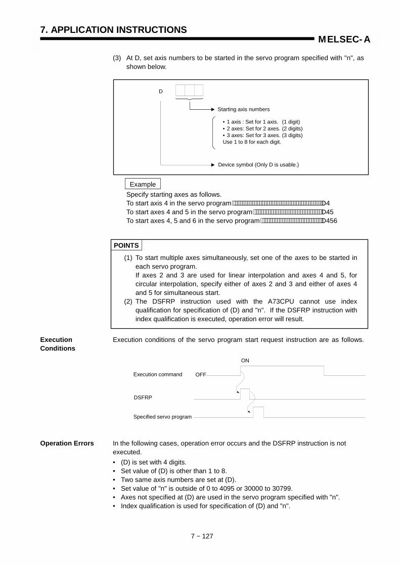
7. APPLICATION INSTRUCTIONS
7 − 127
MELSEC-A
(3) At D, set axis numbers to be started in the servo program specified with "n", asshown below.
ExampleSpecify starting axes as follows.To start axis 4 in the servo program⋅⋅⋅⋅⋅⋅⋅⋅⋅⋅⋅⋅⋅⋅⋅⋅⋅⋅⋅⋅⋅⋅⋅⋅⋅⋅⋅⋅⋅⋅⋅⋅⋅⋅⋅⋅⋅⋅⋅⋅⋅⋅⋅⋅⋅⋅⋅⋅⋅⋅⋅⋅⋅D4To start axes 4 and 5 in the servo program⋅⋅⋅⋅⋅⋅⋅⋅⋅⋅⋅⋅⋅⋅⋅⋅⋅⋅⋅⋅⋅⋅⋅⋅⋅⋅⋅⋅⋅⋅⋅⋅⋅⋅⋅⋅⋅⋅⋅⋅ D45To start axes 4, 5 and 6 in the servo program⋅⋅⋅⋅⋅⋅⋅⋅⋅⋅⋅⋅⋅⋅⋅⋅⋅⋅⋅⋅⋅⋅⋅⋅⋅⋅⋅⋅⋅⋅⋅⋅⋅⋅⋅⋅D456
POINTS
(1) To start multiple axes simultaneously, set one of the axes to be started ineach servo program.If axes 2 and 3 are used for linear interpolation and axes 4 and 5, forcircular interpolation, specify either of axes 2 and 3 and either of axes 4and 5 for simultaneous start.
(2) The DSFRP instruction used with the A73CPU cannot use indexqualification for specification of (D) and "n". If the DSFRP instruction withindex qualification is executed, operation error will result.
Execution Execution conditions of the servo program start request instruction are as follows.Conditions
Operation Errors In the following cases, operation error occurs and the DSFRP instruction is notexecuted.• (D) is set with 4 digits.• Set value of (D) is other than 1 to 8.• Two same axis numbers are set at (D).• Set value of "n" is outside of 0 to 4095 or 30000 to 30799.• Axes not specified at (D) are used in the servo program specified with "n".• Index qualification is used for specification of (D) and "n".
Device symbol (Only D is usable.)
Starting axis numbers
• 1 axis : Set for 1 axis. (1 digit)• 2 axes: Set for 2 axes. (2 digits)• 3 axes: Set for 3 axes. (3 digits)Use 1 to 8 for each digit.
D
Execution command
DSFRP
Specified servo program
ON
OFF

7. APPLICATION INSTRUCTIONS
7 − 128
MELSEC-A
Program Example (1) A program to execute a specified servo program only once when X80 is ON.
• Coding0 LD M90361 OUT M20002 LD X0803 PLS M06 LD M07 SET M18 LD M19 ANI M2001
10 ANI M200211 DSFRP D12 K118 RST M119 END
ABS-2AXIS 1, 10000AXIS 2, 27000SPEED 1000
Servo program( K1 )
2-axis linear interpolationof axes 1 and 2
When execution of the DSFRP instructionis completed, the start request storageflag is reset.
( ) PC READY is ON.
After X80 is turned on, the start requeststorage flag (M1) is set.
If the specified axis is not started, theDSFRP instruction is executed.
0
2
6
8
M9036
X080
M0
M1 M2001 M2002
M2000
PLS M0
SET M1
RST M1
P K DSFR D12 1

7. APPLICATION INSTRUCTIONS
7 − 129
MELSEC-A
(2) A program to execute only once the servo program of which number isspecified with the BCD data at X90 to X9F when X80 is ON.(This servo program is to perform 2-axis linear interpolation of axes 1 and 2.)
• Coding0 LD M90361 OUT M20002 LD X0803 BINP K4X090 D108 PLS M0
11 LD M012 SET M113 LD M114 ANI M200115 ANI M200216 DSFRP D12 K3001023 RST M124 END
ABS-2AXIS 1, 1000AXIS 2, 1000SPEED 1000
ABS-2AXIS 1, 500AXIS 2, 5000SPEED 2000
ABS-2AXIS 1, 3000AXIS 2, 500SPEED 200
( K0 )
Servo program
( K1 )
( K2 )
When execution of the DSFRPinstruction is completed, the startrequest storage flag is reset.
After X80 is turned on, the BCD dataof X90 to X9F are stored in D10 andthe start request storage flag (M1) isset.
( ) PC READY is ON.
If the specified axis is not started, theDSFRP instruction is executed spe-cifying the servo program numberstored in D10.
0
2
11
13
M9036
X080
M0
M1 M2001 M2002
M2000
P K4BIN X090 D10
P K4 DSFR D12 30010
PLS M0
SET M1
RST M1

7. APPLICATION INSTRUCTIONS
7 − 130
MELSEC-A
7.11.2 Present position data and speedchange instruction (DSFLP)
Available Device
Bit device Word (16-bit) device Constant Pointer Level Car
ryfla
g
Erro
rfla
g
X Y M L S B F T C D W R A0 A1 Z V K H P I N
Digi
t spe
cific
atio
n
Inde
x
M9012 (M9010, M9011)
(D) O
n O OO
Functions (1) Either of the processings mentioned below is performed after the DSFLP instruction execution command was turned ON.• Present position data (feed position data) of axes which are currently not
moving are changed to the data of present position data change registers.• Speed data of axes which are moving are changed to the data of speed
change registers.
(2) Axes for present position data/speed change are set with (D) as follows.
ExampleStarting axes are set as follows.• Axis 4 ⋅⋅⋅⋅⋅⋅⋅⋅⋅⋅⋅⋅⋅⋅⋅⋅⋅⋅⋅⋅⋅⋅⋅⋅⋅⋅⋅⋅⋅⋅⋅⋅⋅⋅⋅⋅⋅⋅⋅⋅⋅⋅⋅⋅⋅⋅⋅⋅⋅⋅⋅⋅⋅⋅⋅⋅⋅⋅⋅⋅⋅⋅⋅⋅⋅⋅⋅⋅⋅D4• Interpolation with axes 4 and 5 ⋅⋅⋅⋅⋅⋅⋅⋅⋅⋅⋅⋅⋅⋅⋅⋅⋅⋅⋅⋅⋅⋅⋅⋅⋅ D4 or D5
(3) Select present position data/speed change by setting data at "n" as mentionedbelow.• Present position data change ⋅⋅⋅⋅⋅⋅⋅⋅⋅⋅⋅⋅⋅⋅⋅⋅⋅⋅⋅⋅⋅⋅⋅⋅⋅⋅⋅⋅K0 or H0• Speed change ⋅⋅⋅⋅⋅⋅⋅⋅⋅⋅⋅⋅⋅⋅⋅⋅⋅⋅⋅⋅⋅⋅⋅⋅⋅⋅⋅⋅⋅⋅⋅⋅⋅⋅⋅⋅⋅⋅⋅⋅⋅⋅⋅⋅⋅⋅⋅⋅⋅⋅⋅⋅⋅⋅K1 or H1
POINT
The DSFLP instruction used with the A73CPU cannot use index qualificationfor specification of (D) and "n". If the DSFLP instruction with index qualificationis executed, operation error will result.
AnSAnN
AnSHAn A1FX A3H
A3M A3V AnA
AnU, A2ASA2USH-S1
A2USH boardQCPU-A(A Mode)
A0J2H A2CA52G A73 A3N
boardApplicableCPU
X X X X X X X X X O X
Remark
Execution command
DSFRS (D) n(D)
Axis number for presentposition data/speedchange
nSetting of present positiondata change/speedchange
D
Starting axes number.• Use 1 to 8 for axis number setting.• For interpolation, set either of the interpolation axes.
Device symbol (Only D is usable.)

7. APPLICATION INSTRUCTIONS
7 − 131
MELSEC-A
(4) Present position data change by the DSFLP instruction is performed as follows.1) The start enable flag (M200n)* which corresponds to the axis specified with
(D) is set.2) Present position data is changed to the data of present position data change
registers which correspond to the axes specified with (D).3) When present position data change is completed, the start enable flag
(M200n) is reset.
Present position data change register numbers are provided as follows.
Axis No. Axis 1 Axis 2 Axis 3 Axis 4 Axis 5 Axis 6 Axis 7 Axis 8
Upper date D961 D967 D973 D979 D985 D991 D997 D1003
Lower date D960 D966 D972 D978 D984 D990 D996 D1002
(5) Speed change by the DSFLP instruction is performed as follows.1) The speed changing flag (M200n) which corresponds to the axis specified
with (D) is set.2) Positioning speed currently executed is changed to the data of speed
change registers which correspond to the axes specified with (D).3) The speed changing flag (M202n) is reset.
Speed change register numbers are provided as follows.
Axis No. Axis 1 Axis 2 Axis 3 Axis 4 Axis 5 Axis 6 Axis 7 Axis 8
Upper date D963 D969 D975 D981 D987 D993 D999 D1005
Lower date D962 D968 D974 D980 D986 D992 D998 D1004
Execution Execution conditions of present position data/speed change are as follows.Conditions
Operation Errors In the following cases, an operation error occurs and the DSFLP instruction is not executed.
(1) Set value of (D) is other than 1 to 8.
(2) Set value of "n" is other than 0 TO 4.(When set value of "n" is 2 to 4, see section 7.11.3)
(3) Index qualification is used for specification of (D) and "n".
REMARK
*: "n" stands for the number of axes."n" → "1" when axis 1 is used.
Execution command
DSFLP instruction
ON
OFF

7. APPLICATION INSTRUCTIONS
7 − 132
MELSEC-A
Minor Errors In the following cases, the minor error (control change error) occurs and present position data change or speed change is not executed. The error detection flag (Xn7) is set and the error code is stored in the minor error code areas which correspond to the troubled axis.
(1) For present position data change, the axis specified with (D) has started.(2) For speed change, the axis specified with (D) is executing zero return or
circular interpolation.(3) For speed change, the axis specified with (D) is decelerating.(4) For speed change, the speed specified with "n" is out of the range from 1 to the
speed limit value.
Program Examples DSFLP(1) A program to change present position data of axis 2 to the BCD data set at X90
to XAF when X81 is turned ON.
• Coding24 LD X08125 PLS M1128 LD M1129 SET M1030 LD M1031 ANI M200232 DBINP K8X090 D96641 DSFLP D2 K048 RST M1049 END
The present position data change storage flag(M10) is set when X81 is turned ON.
When axis 2 is not started, the BCD data of X90to XAF are stored in D966 and D967 (presentposition data change registers).
The DSFLP instruction is executed.
The present position data change storage flagis reset.
24
28
30
X081PLS M11
M11SET M10
M10 M2002 P K8DBIN X090 D966
P KDSFL D2 0
RST M10

7. APPLICATION INSTRUCTIONS
7 − 133
MELSEC-A
(2) A program to change positioning speed of axis 2 to the BCD data set at X90 toXAF when X81 is turned ON.
• Coding24 LD X08125 PLS M1128 LD M1129 SET M1030 LD M1031 DBIN K8X090 D96840 DSFLP D2 K147 RST M1048 END
The speed change storage flag (M10) is setwhen X81 is turned ON.
The BCD data of X90 to XAF are stored inD968 and D969 (positioning speed changeregisters).The DSFLP instruction is executed.
The speed change storage flag is reset.
24
28
30
X081PLS M11
M11SET M10
M10 K8DBIN X090 D968
P KDSFL D2 1
RST M10
A − 4
CONTENTS
1. INTRODUCTION ......................................................................................................................1 −−−− 1 ~ 1 −−−− 3
2. INSTRUCTIONS.....................................................................................................................2 −−−− 1 ~ 2 −−−− 24
2.1 Classification...............................................................................................................................2 − 1
2.2 Instruction List.............................................................................................................................2 − 22.2.1 Explanation for instructions lists ....................................................................................2 − 22.2.2 Sequence instructions ...................................................................................................2 − 52.2.3 Basic instructions...........................................................................................................2 − 82.2.4 Application instructions ................................................................................................2 − 16
3. INSTRUCTION STRUCTURE ................................................................................................3 −−−− 1 ~ 3 −−−− 24
3.1 Instruction Structure....................................................................................................................3 − 1
3.2 Bit Processing .............................................................................................................................3 − 33.2.1 1-bit processing..............................................................................................................3 − 33.2.2 Digit specification processing ........................................................................................3 − 3
3.3 Handling of Numeric Values .......................................................................................................3 − 6
3.4 Storing 32-bit Data......................................................................................................................3 − 8
3.5 Index Qualification ....................................................................................................................3 − 103.6 Subset Processing....................................................................................................................3 − 12
3.7 Operation Error .........................................................................................................................3 − 12
3.8 Cautions on Using AnA, A2AS, AnU, QCPU-A (A Mode) and A2USH board..........................3 − 143.8.1 The number of steps used in instructions....................................................................3 − 143.8.2 Instructions of variable functions .................................................................................3 − 163.8.3 Set values for the extension timer and counter ...........................................................3 − 173.8.4 Cautions on using index qualification ..........................................................................3 − 173.8.5 Storing 32-bit data in index registers ...........................................................................3 − 20
3.9 Operation when the OUT Instruction, SET/RST Instruction andPLS/PLF Instruction are from the Same Device .........................................................................3 − 21
4. INSTRUCTION FORMAT .........................................................................................................4 −−−− 1 ~ 4 −−−− 3
5. SEQUENCE INSTRUCTIONS................................................................................................5 −−−− 4 ~ 5 −−−− 41
5.1 Contact Instructions ....................................................................................................................5 − 25.1.1 Operation start, series connection,parallel connection
(LD, LDI, AND, ANI, OR, ORI).......................................................................................5 − 25.2 Connection Instructions ..............................................................................................................5 − 5
5.2.1 Ladder block series connection, parallel connection (ANB, ORB) ................................5 − 55.2.2 Operation result push, read, pop (MPS, MRD, MPP)....................................................5 − 9
5.3 Output Instructions....................................................................................................................5 − 145.3.1 Bit device, timer, counter output (OUT) .......................................................................5 − 145.3.2 Bit device set, reset (SET,RST) ...................................................................................5 − 195.3.3 Edge-triggered differential output (PLS, PLF) .............................................................5 − 235.3.4 Bit device output reverse (CHK) ..................................................................................5 − 25

A − 5
5.4 Shift Instructions .......................................................................................................................5 − 275.4.1 Bit device shift (SFT, SFTP).........................................................................................5 − 27
5.5 Master Control Instructions.......................................................................................................5 − 295.5.1 Master control set, reset (MC, MCR)...........................................................................5 − 29
5.6 Termination Instructions............................................................................................................5 − 335.6.1 Main routine program termination (FEND) ..................................................................5 − 335.6.2 Sequence program termination (END) ........................................................................5 − 35
5.7 Other Instructions......................................................................................................................5 − 375.7.1 Sequence program stop (STOP) .................................................................................5 − 375.7.2 No operation (NOP, NOPLF) .......................................................................................5 − 39
6. BASIC INSTRUCTIONS.........................................................................................................6 −−−− 1 ~ 6 −−−− 89
6.1 Comparison Operation Instructions ............................................................................................6 − 26.1.1 16-bit data comparison (=, <>, >, <=, <, >=)..................................................................6 − 46.1.2 32-bit data comparison (D=, D<>, D>, D<=, D<,D>=) ...................................................6 − 6
6.2 Arithmetic Operation Instructions................................................................................................6 − 86.2.1 BIN 16-bit addition, subtraction (+, +P, -, -P) ...............................................................6 − 106.2.2 BIN 32-bit addition, subtraction (D+, D+P, D-, D-P).....................................................6 − 136.2.3 BIN 16-bit multiplication, division (*, *P, /, /P) ..............................................................6 − 166.2.4 BIN 32-bit multiplication, division (D*, D*P, D/, D/P)....................................................6 − 196.2.5 BCD 4-digit addition, subtraction (B+, B+P, B-, B-P) ...................................................6 − 226.2.6 BCD 8-digit addition, subtraction (DB+, DB+P, DB-, DB-P).........................................6 − 256.2.7 BCD 4-digit multiplication, division (B*, B*P, B/, B/P) ..................................................6 − 286.2.8 BCD 8-digit multiplication, division (DB*, DB*P, DB/, DB/P)........................................6 − 316.2.9 16-bit BIN data increment, decrement (INC, INCP, DEC, DECP) ...............................6 − 346.2.10 32-bit BIN data increment, decrement (DINC, DINCP, DDEC, DDECP).....................6 − 36
6.3 BCD ↔ BIN Conversion Instructions........................................................................................6 − 386.3.1 BIN data → BCD 4-, 8-digit conversion (BCD, BCDP, DBCD, DBCDP) .....................6 − 396.3.2 BCD 4-, 8-digit → BIN data conversion (BIN, BINP, DBIN, DBINP)............................6 − 42
6.4 Data Transfer Instructions.........................................................................................................6 − 466.4.1 16-, 32-bit data transfer (MOV, MOVP, DMOV, DMOVP) ............................................6 − 476.4.2 16-, 32-bit data negation transfer (CML, CMLP, DCML, DCMLP)...............................6 − 496.4.3 16-bit data block transfer (BMOV, BMOVP, FMOV, FMOVP)......................................6 − 526.4.4 16-, 32-bit data exchange (XCH, XCHP, DXCH, DXCHP) ..........................................6 − 56
6.5 Program Branch Instructions ....................................................................................................6 − 586.5.1 Conditional jump, unconditional jump (CJ, SCJ, JMP)................................................6 − 586.5.2 Subroutine call, return (CALL, CALLP, RET)...............................................................6 − 626.5.3 Interrupt enable, disable, return (EI, DI, IRET) ............................................................6 − 646.5.4 Microcomputer program call (SUB, SUBP) .................................................................6 − 67
6.6 Program Switching Instructions ................................................................................................6 − 696.6.1 Main ↔ subprogram switching (CHG).........................................................................6 − 69
A − 6
6.7 Link Refresh Instructions ..........................................................................................................6 − 826.7.1 Link refresh (COM) ......................................................................................................6 − 826.7.2 Link refresh enable, disable (EI, DI) ............................................................................6 − 846.7.3 Partial refresh (SEG) ...................................................................................................6 − 87
7. APPLICATION INSTRUCTIONS..........................................................................................7 −−−− 1 ~ 7 −−−− 133
7.1 Logical Operation Instructions ....................................................................................................7 − 27.1.1 16-, 32-bit data logical product (WAND, WANDP, DAND, DANDP) ..............................7 − 37.1.2 16-, 32-bit data logical add (WOR, WORP, DOR, DORP).............................................7 − 77.1.3 16-, 32-bit data exclusive logical add (WXOR, WXORP, DXOR, DXORP) ................. 7 − 117.1.4 16, 32-bit data NOT exclusive logical add (WXNR, WXNRP, DXNR, DXNRP)...........7 − 157.1.5 BIN 16-bit data 2’s complement (NEG, NEGP) ...........................................................7 − 19
7.2 Rotation Instructions .................................................................................................................7 − 217.2.1 16-bit data right rotation (ROR, RORP, RCR, PCRP) .................................................7 − 227.2.2 16-bit data left rotation (ROL, ROLR, RCL, RCLP) .....................................................7 − 247.2.3 32-bit data right rotation (DROR, DRORP, DRCR, DRCRP).......................................7 − 267.2.4 32-bit data left rotation (DROL, DROLP, DRCL, DRCLP) ...........................................7 − 28
7.3 Shift Instructions .......................................................................................................................7 − 307.3.1 16-bit data n-bit right shift, left shift (SFR, SFRP, SFL, SFLP) ....................................7 − 317.3.2 n-bit data 1-bit right shift, left shift (BSFR, BSFRP, BSFL, BSFLP) ............................7 − 337.3.3 n-word data 1-word right shift, left shift (DSFR, DSFRP, DSFL, DSFLP)....................7 − 35
7.4 Data Processing Instructions ....................................................................................................7 − 377.4.1 16-bit data search (SER, SERP) .................................................................................7 − 387.4.2 16-, 32-bit data bit check (SUM, SUMP, DSUM, DSUMP) ..........................................7 − 407.4.3 8 ↔ 256-bit decode, encode (DECO, DECOP, ENCO, ENCOP)................................7 − 427.4.4 7 segment decode (SEG) ............................................................................................7 − 447.4.5 Word device bit set, reset (BSET, BSETP, BRST, BRSTP) .........................................7 − 467.4.6 16-bit data dissociation, association (DIS, DISP, UNI, UNIP) .....................................7 − 487.4.7 ASCII code conversion (ASC) .....................................................................................7 − 51
7.5 FIFO Instructions ......................................................................................................................7 − 537.5.1 FIFO table write, read (FIFW, FIFWP, FIFR, FIFRP)...................................................7 − 54
7.6 Buffer Memory Access Instructions ..........................................................................................7 − 587.6.1 Special function module 1-, 2-word data read (FROM, FROMP, DFRO, DFROP) .....7 − 597.6.2 Special function module 1-, 2-word data write (TO, TOP, DTO, DTOP)......................7 − 617.6.3 Remote terminal module 1- and 2-word data read
(FROM, PRC, FROMP, PRC, DFRO, PRC, DFROP, PRC) ........................................7 − 637.6.4 Remote terminal module 1- and 2-word data write
(TO, PRC, TOP, PRC, DTO, PRC, DTOP, PRC) .........................................................7 − 677.6.5 Special module/special block 1-, 2-word data read
(FROM, FROMP, DFRO, DFROP) ..............................................................................7 − 717.6.6 Special module/special block 1-, 2-word data write (TO, TOP, DTO, DTOP)..............7 − 74
7.7 FOR to NEXT Instructions ........................................................................................................7 − 777.7.1 FOR to NEXT (FOR, NEXT)........................................................................................7 − 77

A − 7
7.8 Local, Remote I/O Station Access Instructions ........................................................................7 − 797.8.1 Local station data read, write (LRDP, LWTP) ..............................................................7 − 807.8.2 Remote I/O station data read, Write (RFRP, RTOP) ...................................................7 − 86
7.9 Display Instructions...................................................................................................................7 − 927.9.1 ASCII code print instructions (PR, PRC) .....................................................................7 − 947.9.2 ASCII code comment display instructions (LED, LEDC) ...........................................7 − 1007.9.3 Character display instructions (LEDA, LEDB) ...........................................................7 − 1037.9.4 Annunciator reset instruction (LEDR) ........................................................................7 − 105
7.10 Other Instructions....................................................................................................................7 − 1087.10.1 WDT reset (WDT, WDTP)..........................................................................................7 − 1097.10.2 Specific format failure check (CHK)........................................................................... 7 − 1117.10.3 Status latch set, reset (SLT, SLTR)............................................................................ 7 − 1177.10.4 Sampling trace set, reset (STRA, STRAR)................................................................ 7 − 1197.10.5 Carry flag set, reset (STC, CLC)................................................................................7 − 1217.10.6 Pulse regeneration instruction (DUTY)......................................................................7 − 123
7.11 Servo Program Instructions ....................................................................................................7 − 1257.11.1 Servo program start (DSFRP) ...................................................................................7 − 1267.11.2 Present position data and speed change instruction (DSFLP)..................................7 − 130
8. MICROCOMPUTER MODE ...................................................................................................8 −−−− 1 ~ 8 −−−− 16
8.1 Specifications of Microcomputer Mode.......................................................................................8 − 1
8.2 Using Utility Program ..................................................................................................................8 − 2
8.3 Using User-Written Microcomputer Programs............................................................................8 − 48.3.1 Memory map..................................................................................................................8 − 68.3.2 Data memory area address configuration .....................................................................8 − 68.3.3 Differences in operations called by microcomputer instructions
according to CPU models ..............................................................................................8 − 78.3.4 Configuration of data memory area ...............................................................................8 − 8
9. ERROR CODE LIST...............................................................................................................9 −−−− 1 ~ 9 −−−− 41
9.1 Reading Error Codes ..................................................................................................................9 − 1
9.2 Error Code List for the An, AnN, A3H, A3M, A3V, A0J2H, AnS, A2C, A73, A52G, A1FX and A3Nboard...........................................................................................................................................9 − 1
9.3 Error Code List for AnSHCPU ....................................................................................................9 − 7
9.4 Error Code List for the AnACPU...............................................................................................9 − 13
9.5 Error Code List for the AnUCPU, A2ASCPU and A2USH board .............................................9 − 229.6 Error Code List for the QCPU-A (A Mode) ...............................................................................9 − 33
APPENDICES .....................................................................................................................APP −−−− 1 ~ APP −−−− 96
APPENDIX 1 LISTS OF SPECIAL RELAYS AND SPECIAL REGISTERS ...................................APP − 1
1.1 List of Special Relays ............................................................................................................APP − 11.2 Special Relays for Link ........................................................................................................APP − 13
1.3 Special Registers .................................................................................................................APP − 16
1.4 Special Registers for Link ....................................................................................................APP − 34
A − 8
APPENDIX 2 OPERATION PROCESSING TIME........................................................................APP − 392.1 Instruction Processing Time of Small Size, Compact CPUs ...............................................APP − 412.2 Instruction Processing Time of CPUs ..................................................................................APP − 66
2.3 Instruction Processing Time of QCPU-A (A Mode)..............................................................APP − 79
APPENDIX 3 ASCII CODE TABLE...............................................................................................APP − 89APPENDIX 4 FORMATS OF PROGRAM SHEETS .....................................................................APP − 90

8. MICROCOMPUTER MODE
8 − 1
MELSEC-A
8. MICROCOMPUTER MODE
This section gives the microcomputer mode specifications, memory map and datamemory configuration of the ACPU modules. Note that the AnA, A2AS, AnU, QCPU-A (A Mode) and A2USH board cannot use the microcomputer mode.
8.1 Specifications of Microcomputer Mode
Module CPU(Clock)
MicrocomputerProgram Area Work Area Stack Area Instructions which
cannot be used *2
A1 0 to 10K bytes
A2 (S1) 0 to 26K bytes
A3
8086(8 MHz) 0 to 58K bytes (Main)
0 to 58K bytes (Sub)
A1N 0 to 10K bytes
A2N (S1) 0 to 26K bytes
A3N 0 to 58K bytes (Main)0 to 58K bytes (Sub)
A3V 0 to 58K bytes (Main)0 to 58K bytes (Sub)
A73 0 to 58K bytes (Main)0 to 58K bytes (Sub)
A52G
8086(10 MHz)
0 to 14K bytes
A1SH,A1SJH
8086(30 MHz) 0 to 14K bytes
A2SH (S1) 0 to 26K bytes
A1FX8086
(40 MHz) 0 to 26K bytes
A0J2H 0 to 14K bytes
A2C8086
(8 MHz) 0 to 14K bytes
INT, INTO, IRET, IN,OUT, HLT, WAIT,LOCK, ESC
A3H 0 to 58K bytes (Main)0 to 58K bytes (Sub)
A3M
80286(8 MHz) 0 to 58K bytes (Main)
0 to 58K bytes (Sub)
A100H to A1FFH(256 bytes)
User area: 128 bytes (Nosetting required by theuser)
INT, INTO, IRET, IN,OUT, HLT, WAIT,LOCK, ESC, CLI, STI
Table 8.1 Specifications of Microcomputer Mode
*1: Specify the microcomputer program area in multiples of 2K bytes.The relation between the main (sub) program, sequence program, and microcomputer program capacities is as indicated below:
*2: Never use the instructions specified as those which cannot be used in preparingmicrocomputer programs. If they are used, the PC CPU will malfunction when a microcomputer program is run.
Main (sub)program memory
capacity
sequenceprogram memory
capacity
microcomputerprogram memory
capacity= +
*1

8. MICROCOMPUTER MODE
8 − 2
MELSEC-A
8.2 Using Utility Program
Various types of control and operation (e.g. PID control, function operation, codeconversion) can be executed by calling the utility program from the microcomputerprogram area.
(1) Utility program entry procedure
Combine together the utility program with the user program in the followingprocedure:
Fig. 8.1 Entering the Utility Program
1) By loading the SW -GPPA system disk, write the sequence program andset microcomputer capacity of parameters. Then, register the program andthe parameters to the user’s floppy disk.
2) Load the SW -UTLP- system disk into the peripheral device and readthe parameters and sequence program from the user disk to the userprogram area.
3) Read the utility program from the system disk to the utility program area.
4) Combine together the sequence program and utility program in the user userprogram area.
5) Write the combined program onto user disk.
3)
4)1)
2)
5)
Utilityprogram
SW -UTLP- system disk
Utilityprogram
Utilityprogram
Utilityprogram
Parameter+
sequenceprogram
Parameter+
sequenceprogram
System diskfor the
peripheralused (e.g.
SW -GPPA)
Utility program area User program areaInternal memory
Peripheral device with FDD function (e.g. A6GPP)
User disk

8. MICROCOMPUTER MODE
8 − 3
MELSEC-A
(2) Calling the utility program
Call the utility program from the sequence program as described below:
For further information, see the corresponding utility program operating manual.
Call the head address ofthe utility program usingthe SUB instruction.
Specify input data in anyword device (D, W, R)
Specify the data required for program run, device number forstoring the operation result, etc. in any word device.
……
Specify the head devicenumber storing the in-put data in D9090.
The head device number storing the input data should bespecified in D9090 before calling the utility program be-cause D9090 is read to check the input data location whenthe utility program is executed.
……

8. MICROCOMPUTER MODE
8 − 4
MELSEC-A
8.3 Using User-Written Microcomputer Programs
A source program written by the user in the 8086 assembly language is converted toa machine language using assembler commands of CP/M or MS-DOS. Thisconverted program is called "the object program" and is to be stored in themicrocomputer program area of the CPU using the system floppy disk for aperipheral device which has microcomputer mode.
(1) Processes from writing the source program to storing it in the microcomputer program area
The flow chart below describes processes from writing the source program to storingit in the microcomputer program area in the CPU using the CP/M 86 which is bootedwith the SW C-BAS type GPP-BASIC package.
(2) Precautions on preparing the microcomputer program
1) Provide the PUSH instruction at the start of the microcomputer program sothat contents of the registers used during execution are saved in the stackareas. Also, provide the POP instruction at the end of the program so thatthe contents of registers saved in the stack areas are returned.
2) Initialize the registers to be used in the microcomputer program at the startof the microcomputer program. Contents of the registers when themicrocomputer program is called from the sequence program are notdefinite.
3) Since the microcomputer program is executed only when it is called from thesequence program with the SUB(P) instruction, the sequence program isalways required.
4) To return from the microcomputer program to the sequence program, usethe RETF (return to outside the segment) instruction.
CP/M 86 system booting Insert the SW C-BAS system disk in drive A of the A6GPPto boot CP/M 86.
……..
Write the source programusing the ED (text editor)command.
Use the ED command to write the source program in the8086 assembly language, and to store it on a user's floppydisk. (File identifier: .ASM)
……..
Assemble the sourceprogram using the ASM86(assembler) command.
Assemble the source program written in assembly languageand generate the object program using the ASM86command. (File identifier: .HEX)
……..
Generate the load programusing the GENCMD (CMDfile generation) command.
Use the GENCMD command to generate the load programfrom the object program which can be executed. (Fileidentifier: .COM)
……..
Unite the microcomputerprogram with the sequenceprogram using the UPC(unite) command.
Unite the load program which can be executed with thesequence program and store it on a user’s floppy disk usingthe UPS command.
……..

8. MICROCOMPUTER MODE
8 − 5
MELSEC-A
CP/M and CP/M-86 are trademarks of Digital Research, Inc.MS-DOS is a trademark of Microsoft Corporation.
(3) Calling method of microcomputer programThe microcomputer program is called by the execution of SUB instruction in the sequence program.The format of the SUB instruction is as shown below.
Fig. 8.2 Format of SUB Instruction
Example:In the following memory map, the specification of "n" is as shown below.
In the SUB instruction, specify as shown below.
By changing the offset value specified at "n", multiple microcomputer programs canalso be called.
Fig. 8.3 Calling Method for Multiple Microcomputer Programs
n Offset value of microcomputer program to becalled
Setting data
SUB n
Microcomputer program call command
Head address ofmicrocomputer programarea which will be called actually(offset value)
SUB H33F
0H
500H
Microcomputer program
Microcomputer programMicrocomputerprogram mode
Call
Call
SUB H0
SUB H500
Head address ofmicrocomputer programarea (offset value)
Sequence program area
Microcomputer program area
0H33FH
ParameterT/C set value
SUB n
Microcomputer program
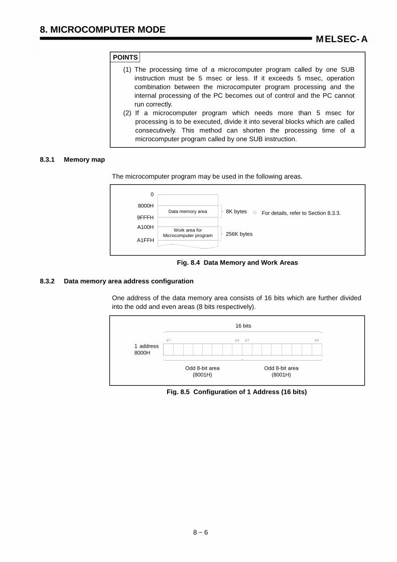
8. MICROCOMPUTER MODE
8 − 6
MELSEC-A
POINTS
(1) The processing time of a microcomputer program called by one SUBinstruction must be 5 msec or less. If it exceeds 5 msec, operationcombination between the microcomputer program processing and theinternal processing of the PC becomes out of control and the PC cannotrun correctly.
(2) If a microcomputer program which needs more than 5 msec forprocessing is to be executed, divide it into several blocks which are calledconsecutively. This method can shorten the processing time of amicrocomputer program called by one SUB instruction.
8.3.1 Memory map
The microcomputer program may be used in the following areas.
8.3.2 Data memory area address configuration
One address of the data memory area consists of 16 bits which are further dividedinto the odd and even areas (8 bits respectively).
Data memory area
Work area forMicrocomputer program
A1FFH
A100H
9FFFH
8000H
0
8K bytes
256K bytes
For details, refer to Section 8.3.3.
Fig. 8.4 Data Memory and Work Areas
b7 b0 b7 b0
16 bits
1 address8000H
Odd 8-bit area(8001H)
Odd 8-bit area(8001H)
Fig. 8.5 Configuration of 1 Address (16 bits)
8. MICROCOMPUTER MODE
8 − 7
MELSEC-A
8.3.3 Differences in operations called by microcomputer instructions according to CPU models
Microcomputer instruction processing operation differs according to the CPU to beused.
(1) REP LODSW, REP LODSB instructions
(a) AnSHCPU and A1FXCPUDisregarding the value at CX register, the contents of memory indicated bythe S1 register are sent only once to AL (8-bit operation) or AX (16-bitoperation) register.
(b) CPU other than AnSHCPU and A1FXCPUThe contents of memory indicated by the S1 register are sent to AL (8-bitoperation) or AX (16-bit operation) register by the number of timesspecified by the CX register.After the execution of the instruction, the value at CX register is cleared to"0".
To use CPU other than AnSHCPU and A1FXCPU same as AnSHCPU andA1FXCPU, refer to the following example program.
CPU other than AnSHCPU and A1FXCPU AnSHCPU and A1FXCPU
STDMOV CX.3REP LODSB
STDMOV CX.3
A: REP LODSBLoop A
<Example program>

8. MICROCOMPUTER MODE
8 − 8
MELSEC-A
8.3.4 Configuration of data memory area
The data memory area (8000H to 9FFFH) stores device data. The memory area ofeach device and its configuration are as indicated below.
Device CPUType Address Configuration
A1A1NA1S
A1SJ(S3)
8000H
to803FH
X0 to FF
A2A2NA2C
A52GA0J2HA1S-S1
A2S
8000H
to807FH
X0 to 1FF
A2-S1A2N-S1A2S-S1
8000Hto
80FFHX0 to 3FFInput
(X)
A3A3NA3VA73
A3N boardA1SHA1SJHA2SH
A2SH-S1A1FX
8000H to81FF H
X0 to 7FF
A1A1NA1S
A1SJ(S3)
8200Hto
823FHY0 to FF
A2A2NA2C
A52GA0J2HA1S-S1
A2S
8000H
to827FH
Y0 to 1FF
A2-S1A2N-S1A2S-S1
8200H
to82FFH
Y0 to 3FFOutput
(Y)
A3A3NA3VA73
A3N boardA1SHA1SJHA2SH
A2SH-S1A1FX
8200H to83FFH
Y0 to 7FF
8200H
8202H
8204H
Odd address Even address
• Used for storing operationresult of PC and allowsread/write.
• Stored data area as follows:0: OFF11: ON
Write
Read Direct modeRefresh mode
Output module
Output refresh after ENDinstruction is executed
Y7 Y6 Y5 Y4 Y3 Y2 Y1 Y0
b15 b8 b7 b6 b5 b4 b3 b2 b1 b0
YF YE YD YC YB YA Y9 Y8
Y17 Y16 Y15 Y14 Y13 Y12 Y11 Y10
Output memory
XIM7 XIM4 X5 X4 X3 X2 X1 X0
b15 b14 b13 b12 b11 b10 b9 b8 b7 b6 b5 b4 b3 b2 b1 b0
XIMF XIME XIMD XIMC XIMB XIMA XIM9 XIM8 XF XE XD XC XB XA X9
XIM3 XIM2 XIM1 XIM0 X7 X6
X8
XIM X17 X16 X15 X14 X13 X12 X11 X10
XIM6 XIM5
XIM XIM XIM XIM XIM XIM XIM1011121314151617
8000H
8002H
8004H
Obtain actual input by thefollowing expression:
Input (X) = (XIM) V (X)
Odd address Even address
• Used for storing ON/OFF datafrom input unit and allows onlyread.
• Stored data area as follows:0: OFF1: ON
• Used for storing ON/OFF datafrom remote station and allowsread/write.
• Stored data area as follows:0: OFF1: ON

8. MICROCOMPUTER MODE
8 − 9
MELSEC-A
REMARK
Communication of input/output information with an input/output module is executed only in theaddress range indicated below.A1FX: X/Y20 to FFA1SH, A1SJH: X/Y0 to FFA2SH: X/Y0 to 1FFA2SH-S1: X/Y0 to 3FF
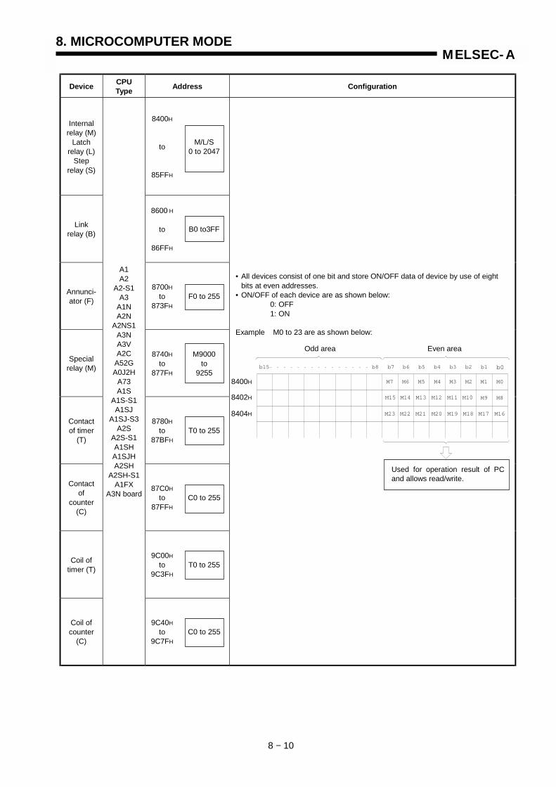
8. MICROCOMPUTER MODE
8 − 10
MELSEC-A
Device CPUType Address Configuration
Internalrelay (M)
Latchrelay (L)
Steprelay (S)
8400H
to
85FFH
M/L/S0 to 2047
Linkrelay (B)
8600 H
to
86FFH
B0 to3FF
Annunci-ator (F)
8700H
to873FH
F0 to 255
Specialrelay (M)
8740H
to877FH
M9000to
9255
Contactof timer
(T)
8780Hto
87BFHT0 to 255
Contactof
counter(C)
87C0Hto
87FFHC0 to 255
Coil oftimer (T)
9C00Hto
9C3FHT0 to 255
Coil ofcounter
(C)
A1A2
A2-S1A3
A1NA2N
A2NS1A3NA3VA2C
A52GA0J2H
A73A1S
A1S-S1A1SJ
A1SJ-S3A2S
A2S-S1A1SHA1SJHA2SH
A2SH-S1A1FX
A3N board
9C40Hto
9C7FHC0 to 255
8400H
8402H
8404H
• All devices consist of one bit and store ON/OFF data of device by use of eight bits at even addresses.
• ON/OFF of each device are as shown below:0: OFF1: ON
Example M0 to 23 are as shown below:
Odd area Even area
Used for operation result of PCand allows read/write.
M7 M6 M5 M4 M3 M2 M1 M0
b15 b8 b7 b6 b5 b4 b3 b2 b1 b0
M15 M9 M8M14 M13 M12 M11 M10
M23 M22 M21 M20 M19 M18 M17 M16

8. MICROCOMPUTER MODE
8 − 11
MELSEC-A
Device CPUType Address Configuration
Dataregister
(D)
8800H to8FFFH
D0to
1023
Linkregister
(W)
9000H to97FFH
W0to
3FF
Presentvalue oftimer (T)
9800H to99FFH
T0to
255
Presentvalue ofcounter
(C)
9A00H to9BFFH
C0to
255
Specialregister
(D)
9D00H to9EFFH
D9000to
9255
Accumu-lator
(A0, 1)
9FF8H to9FFAH
A0
A1
Index(Z, V)
A1A2
A2-S1A3
A1NA2N
A2NS1A3NA3VA2C
A52GA0J2H
A73A1S
A1S-S1A1SJ
A1SJ-S3A2S
A2S-S1A1SHA1SJHA2SH
A2SH-S1A1FX
A3N board
9FFCHto
9FFEH
Z
V
8800H
8001H
(L)
(H)
b7 to b0
b15 to b8
All devices consist of two bytes (16 bits).
Example The configuration of D0 is as shown below:
8800H
8801H
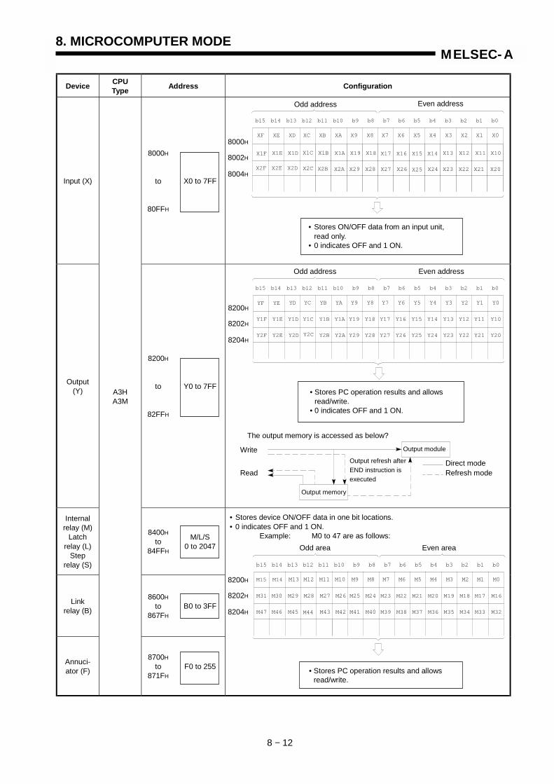
8. MICROCOMPUTER MODE
8 − 12
MELSEC-A
Device CPUType Address Configuration
Input (X)
8000H
to
80FFH
X0 to 7FF
Output(Y)
8200H
to
82FFH
Y0 to 7FF
Internalrelay (M)
Latchrelay (L)
Steprelay (S)
8400Hto
84FFH
M/L/S0 to 2047
Linkrelay (B)
8600Hto
867FHB0 to 3FF
Annuci-ator (F)
A3HA3M
8700Hto
871FHF0 to 255
M15 M14 M12 M5 M4 M3 M2 M1 M0
b15 b14 b13 b12 b11 b10 b9 b8 b7 b6 b5 b4 b3 b2 b1 b0
M30 M29 M28 M27 M26 M25 M24 M23 M22 M21 M20 M19 M18 M17
M13 M11 M10 M9 M8 M7 M6
M16
M46 M45 M43 M42 M41 M40 M39 M38 M37 M36 M35 M34 M33 M32M44
M31
M47
• Stores PC operation results and allows read/write.
• Stores device ON/OFF data in one bit locations.• 0 indicates OFF and 1 ON.
Example: M0 to 47 are as follows:
8200H
8202H
8204H
Odd area Even area
X5 X4 X3 X2 X1 X0
b15 b14 b13 b12 b11 b10 b9 b8 b7 b6 b5 b4 b3 b2 b1 b0
X1F X1E X1D X1C X1B X1A X19 X18 X17 X16 X15 X14 X13 X12 X11
X9 X8 X7 X6
X10
X2A X29 X28 X27 X26 X25 X24 X23 X22 X21 X20
XF XE XD
X2DX2EX2F
XC XB XA
X2C X2B
8000H
8002H
8004H
• Stores ON/OFF data from an input unit, read only.
• 0 indicates OFF and 1 ON.
Odd address Even address
YF YE YC Y5 Y4 Y3 Y2 Y1 Y0
b15 b14 b13 b12 b11 b10 b9 b8 b7 b6 b5 b4 b3 b2 b1 b0
Y1F Y1E Y1D Y1C Y1B Y1A Y19 Y18 Y17 Y16 Y15 Y14 Y13 Y12 Y11
YD YB YA Y9 Y8 Y7 Y6
Y10
Y2F Y2E Y2D Y2C Y2B Y2A Y29 Y28 Y27 Y26 Y25 Y24 Y23 Y22 Y21 Y20
8200H
8202H
8204H
Odd address Even address
• Stores PC operation results and allows read/write.
• 0 indicates OFF and 1 ON.
The output memory is accessed as below?
Write
ReadDirect modeRefresh mode
Output module
Output memory
Output refresh afterEND instruction isexecuted

8. MICROCOMPUTER MODE
8 − 13
MELSEC-A
Device CPUType Address Configuration
Specialrelay (M)
8740Hto
875FH
M9000to
9255
Timer (T)contact
8780H
to879FH
T0 to 255
Counter(C)
contact
87C0H
to87DFH
C0 to 255
Timer (T)coil
9C00H
to9C1FH
T0 to 255
Counter(C) coil
A3HA3M
9C40H
to9C5FH
C0 to 255
• Stores PC operation results andallows read/write.
8400H
8402H
8404H
• Stores device ON/OFF data in one bit locations.• 0 indicates OFF and 1 ON.
Example: M0 to 47 are as follows:
Odd address Even address
M15 M14 M12 M5 M4 M3 M2 M1 M0
b15 b14 b13 b12 b11 b10 b9 b8 b7 b6 b5 b4 b3 b2 b1 b0
M31 M30 M29 M28 M27 M26 M25 M24 M23 M22 M21 M20 M19 M18 M17
M13 M11 M10 M9 M8 M7 M6
M16
M47 M46 M45 M44 M43 M42 M41 M40 M39 M38 M37 M36 M35 M34 M33 M32
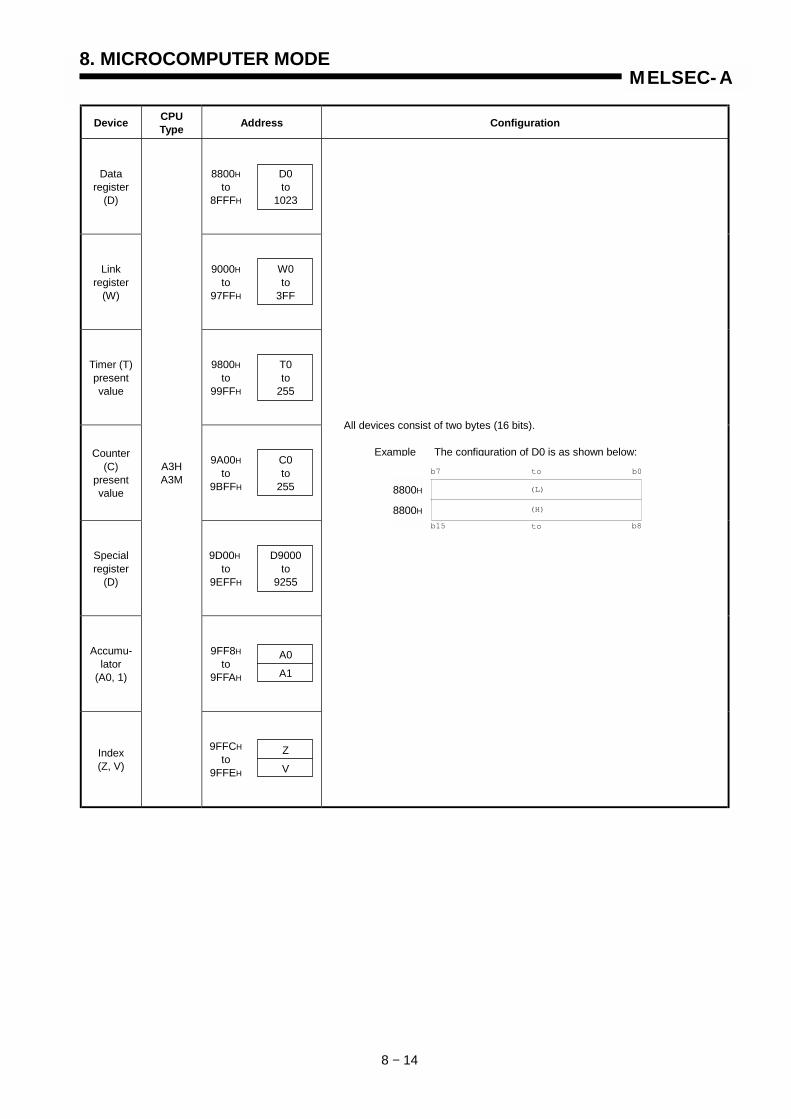
8. MICROCOMPUTER MODE
8 − 14
MELSEC-A
Device CPUType Address Configuration
Dataregister
(D)
8800Hto
8FFFH
D0to
1023
Linkregister
(W)
9000H
to97FFH
W0to
3FF
Timer (T)presentvalue
9800H
to99FFH
T0to
255
Counter(C)
presentvalue
9A00H
to9BFFH
C0to
255
Specialregister
(D)
9D00H
to9EFFH
D9000to
9255
Accumu-lator
(A0, 1)
9FF8Hto
9FFAH
A0
A1
Index(Z, V)
A3HA3M
9FFCHto
9FFEH
Z
V
b7 to b0
8800 H
8001 H
b15 b8
(L)
to
(H)
All devices consist of two bytes (16 bits).
Example The configuration of D0 is as shown below:
8800H
8800H
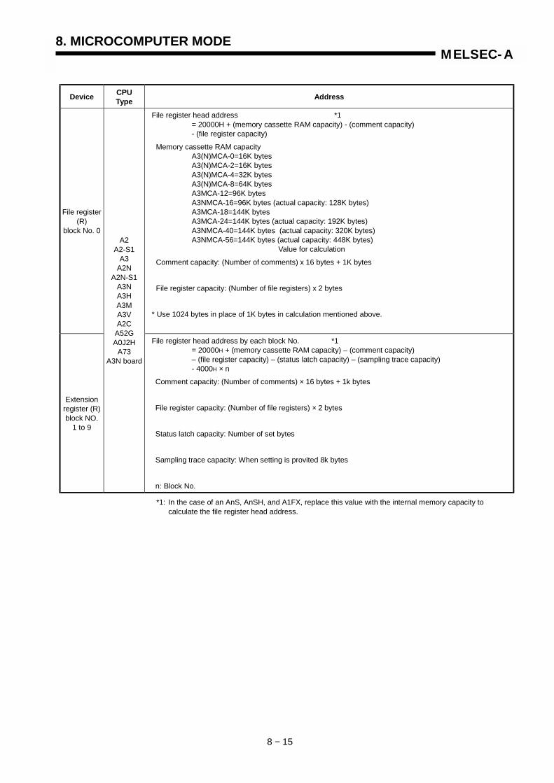
8. MICROCOMPUTER MODE
8 − 15
MELSEC-A
Device CPUType Address
File register(R)
block No. 0
File register head address *1= 20000H + (memory cassette RAM capacity) - (comment capacity)- (file register capacity)
Memory cassette RAM capacityA3(N)MCA-0=16K bytesA3(N)MCA-2=16K bytesA3(N)MCA-4=32K bytesA3(N)MCA-8=64K bytesA3MCA-12=96K bytesA3NMCA-16=96K bytes (actual capacity: 128K bytes)A3MCA-18=144K bytesA3MCA-24=144K bytes (actual capacity: 192K bytes)A3NMCA-40=144K bytes (actual capacity: 320K bytes)A3NMCA-56=144K bytes (actual capacity: 448K bytes)
Value for calculation
Comment capacity: (Number of comments) x 16 bytes + 1K bytes
File register capacity: (Number of file registers) x 2 bytes
* Use 1024 bytes in place of 1K bytes in calculation mentioned above.
Extensionregister (R)block NO.
1 to 9
A2A2-S1
A3A2N
A2N-S1A3NA3HA3MA3VA2C
A52GA0J2H
A73A3N board
File register head address by each block No. *1= 20000H + (memory cassette RAM capacity) – (comment capacity)– (file register capacity) – (status latch capacity) – (sampling trace capacity)- 4000H × n
Comment capacity: (Number of comments) × 16 bytes + 1k bytes
File register capacity: (Number of file registers) × 2 bytes
Status latch capacity: Number of set bytes
Sampling trace capacity: When setting is provited 8k bytes
n: Block No.
*1: In the case of an AnS, AnSH, and A1FX, replace this value with the internal memory capacity to calculate the file register head address.
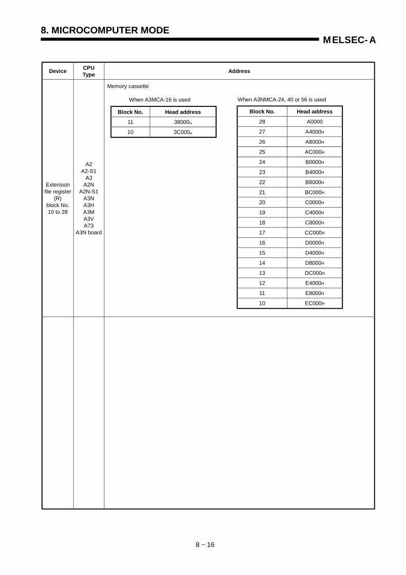
8. MICROCOMPUTER MODE
8 − 16
MELSEC-A
Device CPUType Address
Extensionfile register
(R)block No.10 to 28
A2A2-S1
A3A2N
A2N-S1A3NA3HA3MA3VA73
A3N board
Block No. Head address
11 38000H
10 3C000H
Memory cassette
When A3MCA-16 is used
Block No. Head address
28 A0000
27 A4000H
26 A8000H
25 AC000H
24 B0000H
23 B4000H
22 B8000H
21 BC000H
20 C0000H
19 C4000H
18 C8000H
17 CC000H
16 D0000H
15 D4000H
14 D8000H
13 DC000H
12 E4000H
11 E8000H
10 EC000H
When A3NMCA-24, 40 or 56 is used

9. ERROR CODE LIST
9 − 1
MELSEC-A
9. ERROR CODE LIST
If an error occurred when the PC is in RUN mode, error indication is given by self-checking function and corresponding error code and error step are stored in specialregisters. This section gives description of cause and corrective action for each caseof error.
9.1 Reading Error Codes
If an error occurred, corresponding error code can be read from the peripheral. Fordetails, refer to the operation manual of the peripheral.
9.2 Error Code List for the An, AnN, A3H, A3M, A3V, A0J2H, AnS, A2C, A73, A52G, A1FX and A3Nboard
Table 9.1 shows the error messages, description and cause of error and correctiveactions. Error codes and error steps are stored in the following special registers.
Error code: D9008Error step: D9010 and D9011
Table 9.1 Error Code List for the An, AnN, A3H, A3M, A3V, A0J2H, AnS, A2C, A73, A52G, A1FX andA3N board
Error Message Error Code(D9008)
CPUStates Error and Cause Corrective Action
"INSTRCT.CODE ERR"(Checked at
the execution ofinstruction)
10 Stop Instruction code, which cannot bedecoded by CPU, is included in theprogram.
(1) EP-ROM or memory cassette, which cannot be decoded, has been loaded.
(2) Since the memory contents have changed for some reason, instruction code, which cannot bedecoded, has been included.
(1) Read the error step by use of a peripheral equipment and correct the program at that step.
(2) In the case of EP-ROM or memory cassette, rewrite the contents or replace with an EP-ROM or memory cassette which stores correct contents.
"PARAMETERERROR"
(Checked atpower-on,
STOP → RUN,and
PAUSE → RUN)
11 Stop (1) Capacity larger than the memory capacity of CPU module has been set with the peripheral equipment and then write to CPUmodule has been performed.
(2) The contents of parameters of CPU memory have changed due to noise or the improper loading of memory.
(3) RAM is not loaded to the A1 or A1NCPU.
(1) Check the memory capacity of CPU with the memory capacity set by peripheral equipment and re-set incorrect area.
(2) Check the loading of CPU memory and load it correctly. Read the parameter contents of CPU memory, check and correct the contents, and write them to CPU again.
(3) Install the RAM and write parameter contents from a peripheral device.
"MISSING ENDINS."
(Checked atSTOP → RUN)
12 Stop (1) There is no END ( FEND ) instruction in the program.
(2) When subprogram has been set by the parameter, there is no END instruction in the subprogram.
Write END instruction at the end ofprogram.

9. ERROR CODE LIST
9 − 2
MELSEC-A
Table 9.1 Error Code List for the An, AnN, A3H, A3M, A3V, A0J2H, AnS, A2C, A73, A52G, A1FX andA3N board (Continue)
Error Message Error Code(D9008)
CPUStates Error and Cause Corrective Action
"CAN’TEXECUTE(P)"(Checked at
the execution ofinstruction)
13 Stop (1) There is no jump destination or multiple destinations specified by the CJ , SCJ , CALL , CALLP , or JMP instruction.
(2) There is a CHG instruction and no setting of subprogram.
(3) Although there is no CALL instruction, the RET instruction exists in the program and has been executed.
(4) The CJ , SCJ , CALL , CALL P , or JMP instruction has been executed with its jump destination located below the END instruction.
(5) The number of the FOR instructions is different from that of the NEXT instructions.
(6) A JMP instruction is given withina FOR to NEXT loop causing the processing to exit the loop.
(7) Processing exited subroutine by the JMP instruction before execution of the RET instruction.
(8) Processing jumped into a step in a FOR to NEXT loop or into a subroutine by the JMP instruction.
(9) The STOP instruction is given inan interrupt program, a subroutine program or in a FOR to NEXT loop.
Read the error step by use ofperipheral equipment and correct theprogram at that step.(Insert a jump destination or reducemultiple destinations to one.
"CHK FORMATERR"
(Checked atSTOP/PAUSE→
RUN)
14 Stop (1) Instructions (including NOP ) except LD X , LDI X , AND Xand ANI X are included in the CHK instruction circuit block.
(2) Multiple CHK instructions are given.
(3) The number of contact points in the CHK instruction circuit block exceeds 150.
(4) There is no CJ Pcircuit block before the CHK instruction circuit block.
(5) The device number of D1 of the CHK D1 D2 instruction is different from that of the contact point before the CJ Pinstruction.
(6) Pointer P254 is not given to the head of the CHK instruction circuit block.
CHKP254 D1 D2
Check the program in the CHK instruction circuit blockaccording to items (1) to (6) in the leftcolumn.Correct problem using the peripheraland perform operation again.
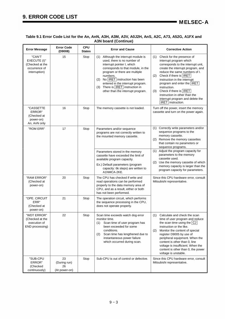
9. ERROR CODE LIST
9 − 3
MELSEC-A
Table 9.1 Error Code List for the An, AnN, A3H, A3M, A3V, A0J2H, AnS, A2C, A73, A52G, A1FX andA3N board (Continue)
Error Message Error Code(D9008)
CPUStates Error and Cause Corrective Action
"CAN’TEXECUTE (I)"
(Checked at theoccurrence ofinterruption)
15 Stop (1) Although the interrupt module is used, there is no number of interrupt pointer I, which corresponds to that module, in theprogram or there are multiple numbers.
(2) No IRET instruction has been entered in the interrupt program.
(3) There is IRET instruction inother than the interrupt program.
(1) Check for the presence of interrupt program which corresponds to the interrupt unit, create the interrupt program, and reduce the same numbers of I.
(2) Check if there is IRET instruction in the interrupt program and enter the IRET instruction.
(3) Check if there is IRET instruction in other than the interrupt program and delete the IRET instruction.
"CASSETTEERROR"
(Checked atpower-on)
An, AnN only
16 Stop The memory cassette is not loaded. Turn off the power, insert the memorycassette and turn on the power again.
Parameters and/or sequenceprograms are not correctly written tothe mounted memory cassette.
(1) Correctly write parameters and/orsequence programs to thememory cassette.
(2) Remove the memory cassettesthat contain no parameters orsequence programs.
"ROM ERR" 17 Stop
Parameters stored in the memorycassette have exceeded the limit ofavailable program capacity.
Ex.) Default parameters (programcapacity: 6k steps) are written toA1NMCA-2KE.
(1) Adjust the program capacity forparameters to the memorycassette used.
(2) Use the memory cassette of whichmemory capacity is larger than theprogram capacity for parameters.
"RAM ERROR"(Checked atpower-on)
20 Stop The CPU has checked if write andread operations can be performedproperly to the data memory area ofCPU, and as a result, either or bothhas not been performed.
"OPE. CIRCUITERR"
(Checked atpower-on)
21 Stop The operation circuit, which performsthe sequence processing in the CPU,does not operate properly.
Since this CPU hardware error, consultMitsubishi representative.
"WDT ERROR"(Checked at the
execution ofEND processing)
22 Stop Scan time exceeds watch dog errormonitor time.(1) Scan time of user program has
been exceeded for some conditions.
(2) Scan time has lengthened due to instantaneous power failure which occurred during scan.
(1) Calculate and check the scan time of user program and reduce the scan time using the CJ instruction or the like.
(2) Monitor the content of special register D9005 by use of peripheral equipment. When the content is other than 0, line voltage is insufficient. When the content is other than 0, the powervoltage is unstable.
"SUB-CPUERROR"(Checked
continuously)
23(During run)
26(At power-on)
Stop Sub-CPU is out of control or defective. Since this CPU hardware error, consultMitsubishi representative.

9. ERROR CODE LIST
9 − 4
MELSEC-A
Table 9.1 Error Code List for the An, AnN, A3H, A3M, A3V, A0J2H, AnS, A2C, A73, A52G, A1FX andA3N board (Continue)
Error Message Error Code(D9008)
CPUStates Error and Cause Corrective Action
"END NOTEXECUTE"
(Checked at theexecution of
END instruction)
24 Stop (1) When the END instruction wasto be executed, the instructionwas read as other instructioncode due to noise or the like.
(2) The END instruction has changed to another instruction code for some reason.
Perform reset and run.If the same error is displayed again, itis the CPU hardware error, consultMitsubishi representative.
"WDT ERROR"(Checked
continuously)
25 Stop The CPU is executing an endless loop. Since the program is in an endless lopdue to the JMP and CJ instructions,check the program.
"MAIN CPUDOWN"
(Checkedcontinuously)
26 Stop Main-CPU is out of control ordefective. (Sub-CPU checked it.)
Since this is a CPU hardware error,consult Mitsubishi representative.
"UNITVERIFY ERR. "
(Checkedcontinuously)
31 Stop orContinue(set bypara-meter)
I/O module data are different fromthose at power-on.The I/O module (including the specialfunction module) is incorrectly loadedor has been removed, or a differentunit has been loaded.
(1) Among special registers D9116 toD9123, the bit corresponding to the module of verify error is "1". Therefore, use peripheral equipment to monitor the registers and check for the module with “1” and make replacement.
(2) When the present unit arrangement is OK, perform resetwith the reset switch.
A fuse is blown in an output module. (1) Check the fuse blown indicator LED of output module and change the fuse of module of which LED is on.
(2) Among special registers D9100 toD9107, the bit corresponding to the unit of fuse break is "1" Replace the fuse of a corresponding module.Monitor and check it.
"FUSE BREAKOFF"
(Checkedcontinuously)
32 Stop orContinue(set bypara-meter)
The external output supply for AnSoutput load is not turned off or notconnected.
Check if the external power supply foroutput load is turned on or off.
"CONTROL-BUS ERR. "
(Checked at theexecution of
FROM and TOinstructions)
40 Stop The FROM and TO instructionscan-not be executed.Error of control bus with specialfunction module.
Since this is a hardware error of aspecial function module, CPU module,or base unit, replace the module andcheck the defective module, consultMitsubishi representative.
"SP. UNITDOWN"
(Checked at theexecution of
FROM and TOinstructions.)
41 Stop When the FROM or TO instructionis executed, access has been made tothe special function module but theanswer is not given.The accessed special function moduleis defective.
Since this is an accessed specialfunction module error, consultMitsubishi representative.
"LINK UNITERROR"
42 Stop The data link module is loaded in themaster station.
Remove the data link module from themaster station. After correction, resetand start from the initialization.

9. ERROR CODE LIST
9 − 5
MELSEC-A
Table 9.1 Error Code List for the An, AnN, A3H, A3M, A3V, A0J2H, AnS, A2C, A73, A52G, A1FX andA3N board (Continue)
Error Message Error Code(D9008)
CPUStates Error and Cause Corrective Action
"I/O INT.ERROR"
43 Stop Although the interrupt module is notloaded, interruption has occurred.
Since this is a hardware error of aspecific module, replace the moduleand check the defective module,consult Mitsubishi representative.
"SP. UNIT LAY.ERROR."
44 Stop (1) Three or more computer link unitsare loaded with respect to oneCPU module.(A1SCPU24-R2 is also counted as one unit.)
(2) Two or more data link modules are loaded.
(3) Two or more interrupt units are loaded.
(4) A special function module is assigned in place of an I/O module, or vice versa, at I/O assignment of parameters on peripheral devices.
(5) The input/output modules or special function modules are loaded at the input/output numbers exceeding the number of input/output points, or GOT is connected via bus line.
(1) Reduce the computer link modules to two or less.
(2) Reduce the data link modules to one or less.
(3) Reduce the interrupt module to one.
(4) Re-set the I/O assignment of parameter setting by use of peripheral devices according to the actually loaded special function module.
(5) Review the input/output numbers,and remove the modules at the input/output numbers beyond the number of input/output points or GOT.
"SP. UNITERROR"
(Checked at theexecution of
FROM and TOinstructions)
46 Stop orContinue(set bypara-meter)
Access (execution of FROM to TO instruction) has been made to alocation where there is not specialfunction unit.
Read the error step by use ofperipheral equipment, and check andcorrect the content of FROM or TO instruction at that step.
"LINK PARA.ERROR"
47 Continue (1) If a data link CPU is used to set a master station (station number "00") : The contents written to the parameter area of link by setting the link range in the parameter setting of peripheral devices are different from the link parameter contents for some reason. Or, linkparameters are not written.
(2) The setting of the total number of slave stations is 0.
(1) Write parameters again and make check.
(2) Check setting of station numbers.
(3) When the error is displayed again, it is hardware error. Therefore, consult Mitsubishi representative.
"OPERATIONERROR"
(Checked duringexecution ofinstruction)
50 Continue (1) The result of BCD conversion has exceeded the specified range(9999 or 99999999).
(2) Operation impossible because specified device range has been exceeded.
(3) File registers used in program without capacity setting.
(4) Operation error occurred during execution of the RTOP , RFRP , LWTP or LRDP instruction.
Read the error step using peripheraldevices and check the program at theerror step, and correct it.(Check the specified device range,BCD conversion, or the like.)

9. ERROR CODE LIST
9 − 6
MELSEC-A
Table 9.1 Error Code List for the An, AnN, A3H, A3M, A3V, A0J2H, AnS, A2C, A73, A52G, A1FX andA3N board (Continue)
Error Message Error Code(D9008)
CPUStates Error and Cause Corrective Action
"MAIN CPUDOWN"
(Interrupt fault)AnNCPU only
60 Stop (1) INT instruction processed in microcomputer program area.
(2) CPU malfunction due to noise.(3) Hardware error of CPU module.
(1) Because the INT instruction cannot be used in the microcomputer program, remove it.
(2) Take measures against noises.(3) Replace the CPU module.
"BATTERYERROR"
(Checked atpower-on)
70 Continue (1) The battery voltage has dropped to below the specified value.
(2) The lead connector of the battery is not connected.
(1) Replace battery.(2) Connect the lead connector if
RAM memory or power failure compensation function is used.
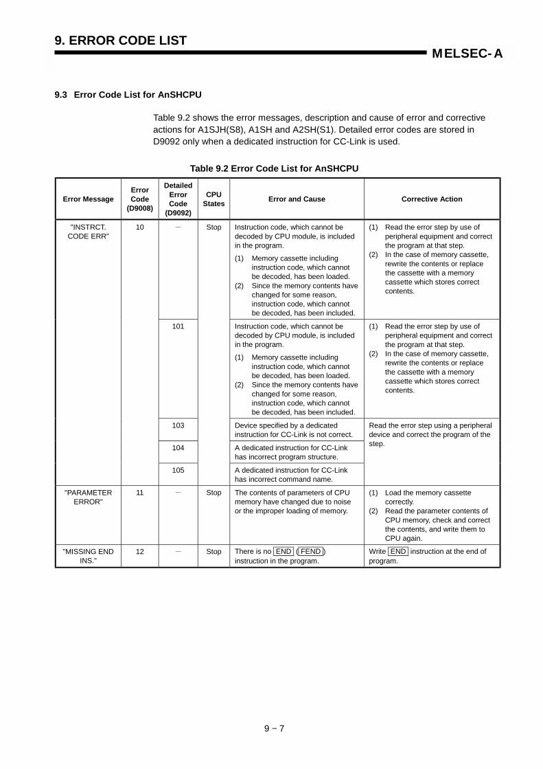
9. ERROR CODE LIST
9 − 7
MELSEC-A
9.3 Error Code List for AnSHCPU
Table 9.2 shows the error messages, description and cause of error and correctiveactions for A1SJH(S8), A1SH and A2SH(S1). Detailed error codes are stored inD9092 only when a dedicated instruction for CC-Link is used.
Table 9.2 Error Code List for AnSHCPU
Error MessageErrorCode
(D9008)
DetailedErrorCode
(D9092)
CPUStates Error and Cause Corrective Action
Instruction code, which cannot bedecoded by CPU module, is includedin the program.
(1) Memory cassette including instruction code, which cannot be decoded, has been loaded.
(2) Since the memory contents havechanged for some reason, instruction code, which cannot be decoded, has been included.
(1) Read the error step by use of peripheral equipment and correct the program at that step.
(2) In the case of memory cassette, rewrite the contents or replace the cassette with a memory cassette which stores correct contents.
101 Instruction code, which cannot bedecoded by CPU module, is includedin the program.
(1) Memory cassette including instruction code, which cannot be decoded, has been loaded.
(2) Since the memory contents havechanged for some reason, instruction code, which cannot be decoded, has been included.
(1) Read the error step by use of peripheral equipment and correct the program at that step.
(2) In the case of memory cassette, rewrite the contents or replace the cassette with a memory cassette which stores correct contents.
103 Device specified by a dedicatedinstruction for CC-Link is not correct.
104 A dedicated instruction for CC-Linkhas incorrect program structure.
"INSTRCT.CODE ERR"
10
105
Stop
A dedicated instruction for CC-Linkhas incorrect command name.
Read the error step using a peripheraldevice and correct the program of thestep.
"PARAMETERERROR"
11 Stop The contents of parameters of CPUmemory have changed due to noiseor the improper loading of memory.
(1) Load the memory cassette correctly.
(2) Read the parameter contents of CPU memory, check and correct the contents, and write them to CPU again.
"MISSING ENDINS."
12 Stop There is no END ( FEND )instruction in the program.
Write END instruction at the end ofprogram.

9. ERROR CODE LIST
9 − 8
MELSEC-A
Table 9.2 Error Code List for AnSHCPU (Continue)
Error MessageErrorCode
(D9008)
DetailedErrorCode
(D9092)
CPUStates Error and Cause Corrective Action
"CAN’TEXECUTE(P)"
13 Stop (1) There is no jump destination or multiple destinations specified bythe CJ , SCJ , CALL , CALLP , or JMP instruction.
(2) Although there is no CALL instruction, the RET instruction exists in the program and has been executed.
(3) The CJ , SCJ , CALL , CALLP , or JMP instructionhas been executed with its jump destination located below the END instruction.
(4) The number of the FOR instructions is different from that of the NEXT instructions.
(5) A JMP instruction is given within a FOR to NEXT loop causing the processing to exit
the loop.(6) Processing exited subroutine by
the JMP instruction before execution of the RET instruction.
(7) Processing jumped into a step in a FOR to NEXT loop or into a subroutine by the JMP instruction.
Read the error step by use ofperipheral equipment and correct theprogram at that step.(Insert a jump destination or reducemultiple destinations to one.)
"CHK FORMATERR"
14 Stop (1) Instructions (including NOP ) except LD X , LDI X , AND Xand ANI X are included in the CHK instruction circuit block.
(2) Multiple CHK instructions are given.
(3) The number of contact points in the CHK instruction circuit blockexceeds 150.
(4) There is no CJ Pcircuit block before the CHK instruction circuit block.
(5) The device number of D1 of the CHK D1 D2 instruction is different from that of the contact point before the CJ Pinstruction.
(6) Pointer P254 is not given to the head of the CHK instruction circuit block.
CHKP254 D1 D2
(1) Check the program in the CHKinstruction circuit block according to item (1) to (7) in the left column.Correct problem using the peripheral equipment and performoperation again.
(2) This error code is only effective when the input/output control method is a direct method.

9. ERROR CODE LIST
9 − 9
MELSEC-A
Table 9.2 Error Code List for AnSHCPU (Continue)
Error MessageErrorCode
(D9008)
DetailedErrorCode
(D9092)
CPUStates Error and Cause Corrective Action
"CAN’TEXECUTE (I)"
15 Stop (1) Although the interrupt module is used, there is no number of interrupt pointer I, which corresponds to that module, in theprogram or there are multiple numbers.
(2) No IRET instruction has been entered in the interrupt program.
(3) There is IRET instruction inother than the interrupt program.
(1) Check for the presence of interrupt program which corresponds to the interrupt unit, create the interrupt program, and reduce the same numbers of I.
(2) Check if there is IRET instruction in the interrupt program and enter the IRET instruction.
(3) Check if there is IRET instruction in other than the interrupt program and delete the IRET instruction.
Parameters and/or sequenceprograms are not correctly written tothe mounted memory cassette.
(1) Correctly write parameters and/orsequence programs to thememory cassette.
(2) Remove the memory cassettesthat contain no parameters orsequence programs.
"ROM ERR" 17 Stop
Parameters stored in the memorycassette have exceeded the limit ofavailable program capacity.
Ex.) Default parameters (programcapacity: 6k steps) are written toA1NMCA-2KE.
(1) Adjust the program capacity forparameters to the memorycassette used.
(2) Use the memory cassette of whichmemory capacity is larger than theprogram capacity for parameters.
"RAM ERROR" 20 Stop The CPU has checked if write andread operations can be performedproperly to the data memory area ofCPU, and as a result, either or bothhas not been performed.
"OPE. CIRCUITERR"
21 Stop The operation circuit, which performsthe sequence processing in the CPU,does not operate properly.
Since this CPU hardware error, consultMitsubishi representative.
"WDT ERROR" 22 Stop Scan time exceeds watch dog errormonitor time.(1) Scan time of user program has
been exceeded for some conditions.
(2) Scan time has lengthened due to instantaneous power failure which occurred during scan.
(1) Calculate and check the scan time of user program and reduce the scan time using the CJ instruction or the like.
(2) Monitor the content of special register D9005 by use of peripheral equipment. When the content is other than 0, line voltage is insufficient. When the content is other than 0, the powervoltage is unstable.
"END NOTEXECUTE"
24 Stop (1) When the END instruction wasto be executed, the instructionwas read as other instructioncode due to noise or the like.
(2) The END instruction has changed to another instruction code for some reason.
Reset and run the CPU module again.If the same error is displayed again, itis the CPU hardware error, consultMitsubishi representative.
"WDT ERROR" 25 Stop The CJ instruction or the like causesa loop in execution of the sequenceprogram to disable execution of the END instruction.
Check the program for an endless loopand correct.

9. ERROR CODE LIST
9 − 10
MELSEC-A
Table 9.2 Error Code List for AnSHCPU (Continue)
Error MessageErrorCode
(D9008)
DetailedErrorCode
(D9092)
CPUStates Error and Cause Corrective Action
"UNITVERIFY ERR."
31 Stopor
Continue
(set bypara-
meter)
I/O module data are different fromthose at power-on.
(1) The I/O module (including the special function module) is incorrectly loaded or has been removed, or a different unit has been loaded.
(1) The bit in special registers D9116 to D9123 corresponding to the module causing the verification error is “1.” Use a peripheral device to monitor the registers to locate the “1” bit, and check or replace the corresponding module.
(2) To accept the current module arrangement, operate the RUN/STOP key switch to reset.
"FUSE BREAKOFF"
32 Stopor
Continue
(set bypara-
meter)
(1) The fuse is blown in some outputmodules.
(2) The external power supply for the output load is turned off or it is disconnected.
(1) Check the ERR LED of the outputmodule. Replace the module with the lit LED.
(2) Among special registers D9100 toD9107, the bit corresponding to the unit of fuse break is "1" Replace the fuse of a corresponding module.Monitor and check it.
(3) Check ON/OFF of the external power supply for the output load.
"CONTROL-BUS ERR."
40 Stop The FROM and TO instructionscannot be executed.(1) Error of control bus with special
function module.
The hardware of the special functionmodule, CPU module or base unit isfaulty. Replace the faulty module andcheck the faulty module. ConsultMitsubishi representative.
"SP. UNITDOWN"
41 Stop There is no reply from the specialfunction module during execution ofthe FROM or TO instruction.(1) The special function module
being accessed is faulty.
The hardware of the special functionmodule being accessed is faulty.Consult Mitsubishi representative.
"I/O INT.ERROR"
43 Stop Interrupt occurs though no interruptmodule is installed.
The hardware of a module is faulty.Replace the module and check thefaulty module. Consult Mitsubishirepresentative.
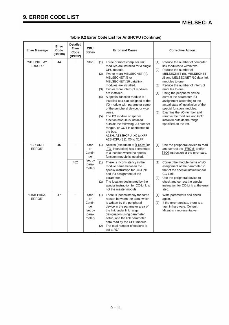
9. ERROR CODE LIST
9 − 11
MELSEC-A
Table 9.2 Error Code List for AnSHCPU (Continue)
Error MessageErrorCode
(D9008)
DetailedErrorCode
(D9092)
CPUStates Error and Cause Corrective Action
"SP. UNIT LAY.ERROR."
44 Stop (1) Three or more computer link modules are installed for a singleCPU module.
(2) Two or more MELSECNET (II), MELSECNET /B or MELSECNET /10 data link modules are installed.
(3) Two or more interrupt modules are installed.
(4) A special function module is installed to a slot assigned to the I/O module with parameter setup of the peripheral device, or vice versa.
(5) The I/O module or special function module is installed outside the following I/O number ranges, or GOT is connected to the bus.A1SH, A1SJHCPU: X0 to XFFA2SHCPU(S1): X0 to X1FF
(1) Reduce the number of computer link modules to within two.
(2) Reduce the number of MELSECNET (II), MELSECNET /B and MELSECNET /10 data linkmodules to one.
(3) Reduce the number of interrupt modules to one.
(4) Using the peripheral device, correct the parameter I/O assignment according to the actual state of installation of the special function modules.
(5) Examine the I/O number and remove the modules and GOT installed outside the range specified on the left.
(1) Access (execution of FROM or TO instruction) has been madeto a location where no special function module is installed.
(1) Use the peripheral device to read and correct the FROM and/or TO instruction at the error step.
"SP. UNITERROR"
46
462
Stopor
Continue
(set bypara-
meter)
(1) There is inconsistency in the module name between the special instruction for CC-Link and I/O assignment of the parameter.
(2) The location designated by the special instruction for CC-Link is not the master module.
(1) Correct the module name of I/O assignment of the parameter to that of the special instruction for CC-Link.
(2) Use the peripheral device to check and correct the special instruction for CC-Link at the errorstep.
"LINK PARA.ERROR"
47 Stopor
Continue
(set bypara-
meter)
(1) There is inconsistency for some reason between the data, which is written by the peripheral device in the parameter area of the link under link range designation using parameter setup, and the link parameter data read by the CPU module.
(2) The total number of stations is set at “0.”
(1) Write parameters and check again.
(2) If the error persists, there is a fault in hardware. Consult Mitsubishi representative.

9. ERROR CODE LIST
9 − 12
MELSEC-A
Table 9.2 Error Code List for AnSHCPU (Continue)
Error MessageErrorCode
(D9008)
DetailedErrorCode
(D9092)
CPUStates Error and Cause Corrective Action
(1) The result of BCD conversion exceeds the rated range ("9999"or "99999999").
(2) There is a setting exceeding the rated device range, disabling execution of calculation.
(3) The file register is used on the program without designation of the capacity of the file register.
Use the peripheral device to read andcorrect the error step in the program.(Check the setting range of the device,BCD conversion value and so on.)
503 The data stored by the designateddevice or a constant exceeds theallowable range.
504 The setting quantity of handled dataexceeds the allowable range.
Use the peripheral device to read andcorrect the error step in the program.
The number of special instructions forCC-Link executed in each scanexceeds 64.
Reduce the special instructions forCC-Link executed in each scan towithin 64.
"OPERATIONERROR"
50
509
Stopor
Continue
(set bypara-
meter)
A special instruction for CC-Link isexecuted to a CC-Link module towhich no parameter is defined.
Define parameters.
"BATTERYERROR"
70 Continue
(1) The battery voltage is low.(2) The battery lead connector is not
connected.
(1) Replace the battery.(2) Connect the lead connector to
use the built-in RAM memory or power failure compensation function.
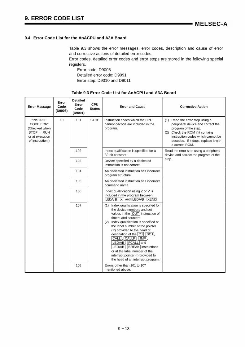
9. ERROR CODE LIST
9 − 13
MELSEC-A
9.4 Error Code List for the AnACPU and A3A Board
Table 9.3 shows the error messages, error codes, description and cause of errorand corrective actions of detailed error codes.Error codes, detailed error codes and error steps are stored in the following specialregisters.
Error code: D9008Detailed error code: D9091Error step: D9010 and D9011
Table 9.3 Error Code List for AnACPU and A3A Board
Error MassageErrorCode
(D9008)
DetailedErrorCode
(D9091)
CPUStates Error and Cause Corrective Action
101 Instruction codes which the CPUcannot decode are included in theprogram.
(1) Read the error step using a peripheral device and correct the program of the step.
(2) Check the ROM if it contains instruction codes which cannot be decoded. If it does, replace it witha correct ROM.
102 Index qualification is specified for a32-bit constant.
103 Device specified by a dedicatedinstruction is not correct.
104 An dedicated instruction has incorrectprogram structure.
105 An dedicated instruction has incorrectcommand name.
106 Index qualification using Z or V isincluded in the program betweenLEDA/ B IX and LEDA/B IXEND.
107 (1) Index qualification is specified forthe device numbers and set values in the OUT instruction oftimers and counters.
(2) Index qualification is specified at the label number of the pointer (P) provided to the head of destination of the CJ , SCJ , CALL , CALLP , JMP , LEDA/B , FCALL and LEDA/B , BREAK instructions or at the label number of the interrupt pointer (I) provided to the head of an interrupt program.
"INSTRCTCODE ERR"
(Checked whenSTOP → RUNor at executionof instruction.)
10
108
STOP
Errors other than 101 to 107mentioned above.
Read the error step using a peripheraldevice and correct the program of thestep.
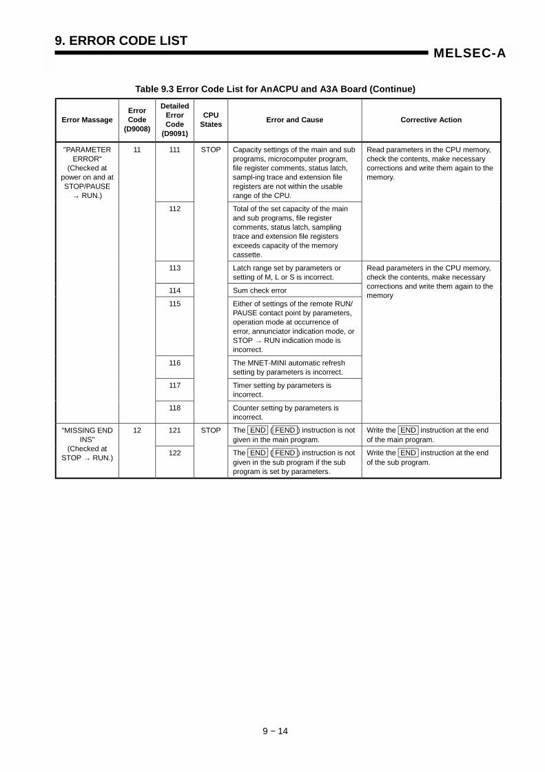
9. ERROR CODE LIST
9 − 14
MELSEC-A
Table 9.3 Error Code List for AnACPU and A3A Board (Continue)
Error MassageErrorCode
(D9008)
DetailedErrorCode
(D9091)
CPUStates Error and Cause Corrective Action
111 Capacity settings of the main and subprograms, microcomputer program,file register comments, status latch,sampl-ing trace and extension fileregisters are not within the usablerange of the CPU.
112 Total of the set capacity of the mainand sub programs, file registercomments, status latch, samplingtrace and extension file registersexceeds capacity of the memorycassette.
Read parameters in the CPU memory,check the contents, make necessarycorrections and write them again to thememory.
113 Latch range set by parameters orsetting of M, L or S is incorrect.
114 Sum check error
115 Either of settings of the remote RUN/PAUSE contact point by parameters,operation mode at occurrence oferror, annunciator indication mode, orSTOP → RUN indication mode isincorrect.
116 The MNET-MINI automatic refreshsetting by parameters is incorrect.
117 Timer setting by parameters isincorrect.
"PARAMETERERROR"
(Checked atpower on and atSTOP/PAUSE
→ RUN.)
11
118
STOP
Counter setting by parameters isincorrect.
Read parameters in the CPU memory,check the contents, make necessarycorrections and write them again to thememory
121 The END ( FEND ) instruction is notgiven in the main program.
Write the END instruction at the endof the main program.
"MISSING ENDINS"
(Checked atSTOP → RUN.)
12
122
STOP
The END ( FEND ) instruction is notgiven in the sub program if the subprogram is set by parameters.
Write the END instruction at the endof the sub program.

9. ERROR CODE LIST
9 − 15
MELSEC-A
Table 9.3 Error Code List for AnACPU and A3A Board (Continue)
Error MassageErrorCode
(D9008)
DetailedErrorCode
(D9091)
CPUStates Error and Cause Corrective Action
131 The same device number is used attwo or more steps for the pointers (P)and interrupt pointers (I) used aslabels to be specified at the head ofjump destination.
Eliminate the same pointer numbersprovided at the head of jumpdestination.
132 Label of the pointer (P) specified inthe CJ , SCJ , CALL , CALLP , JMP ,LEDA/ B FCALL or LEDA/ B BREAKinstruction is not provided before the END instruction.
Read the error step using a peripheraldevice, check contents and insert ajump destination pointer (P).
133 (1) The RET instruction was included in the program and executed though the CALL instruction was not given.
(2) The NEXT LEDA/ B BREAKinstructions were included in the program and executed though the FOR instruction was not given.
(3) Nesting level of the CALL , CALLP and FOR instructions is 6 levels or deeper, and the 6th level was executed.
(4) There is no RET or NEXT instruction at execution of the CALL or FOR instruction.
(1) Read the error step using a peripheral device, check contents and correct program of the step.
(2) Reduce the number of nesting levels of the CALL , CALLP and FOR instructions to 5 or less.
134 The CHG instruction was included inthe program and executed though nosub program was provided.
Read the error step using a peripheraldevice and delete the CHG instructioncircuit block.
"CAN'TEXECUTE (P)"
(Checked atexecution ofinstruction.)
13
135
STOP
(1) LEDA/ B IX and LEDA/B IXEND instructions arenot paired.
(2) There are 33 or more sets ofLEDA/ B IX and LEDA/B IXEND instructions.
(1) Read the error step using a peripheral device, check contents and correct program of the step.
(2) Reduce the number of sets ofLEDA/ B IX and LEDA/B IXEND instructions to 32or less.

9. ERROR CODE LIST
9 − 16
MELSEC-A
Table 9.3 Error Code List for AnACPU and A3A Board (Continue)
Error MassageErrorCode
(D9008)
DetailedErrorCode
(D9091)
CPUStates Error and Cause Corrective Action
141 Instructions (including NOP ) otherthan LDX , LDIX , ANDX and ANIX are included in the CHKinstruction circuit block.
142 Multiple CHK instructions are given.
143 The number of contact points in the CHK instruction circuit blockexceeds 150.
144 The LEDA CHK instructions are notpaired with the LEDA CHKENDinstructions, or 2 or more pairs ofthem are given.
145 Format of the block shown below,which is provided before the CHKinstruction circuit block, is not asspecified.
CJP254 P
146 Device number of D1 in theCHK D1 D2 instruction is differentfrom that of the contact point beforethe CJ P instruction.
147 Index qualification is used in thecheck pattern circuit.
"CHK FORMATERR"
(Checked atSTOP/PAUSE
→ RUN.)
14
148
STOP
(1) Multiple check pattern circuits of the LEDA CHK - LEDA CHKENDinstructions are given.
(2) There are 7 or more check condition circuits in theLEDA CHK - LEDA CHKENDinstructions.
(3) The check condition circuits in the LEDA CHK - LEDA CHKENDinstructions are written without using X and Y contact instructions or compare instructions.
(4) The check pattern circuits of the LEDA CHK - LEDA CHKENDinstructions are written with 257 or more steps.
Check the program of the CHKinstruction and correct it referring tocontents of detailed error codes.
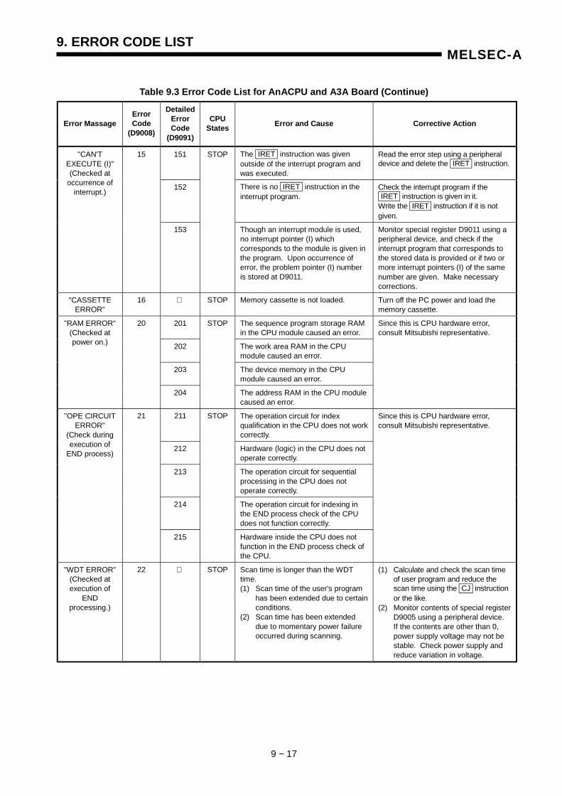
9. ERROR CODE LIST
9 − 17
MELSEC-A
Table 9.3 Error Code List for AnACPU and A3A Board (Continue)
Error MassageErrorCode
(D9008)
DetailedErrorCode
(D9091)
CPUStates Error and Cause Corrective Action
151 The IRET instruction was givenoutside of the interrupt program andwas executed.
Read the error step using a peripheraldevice and delete the IRET instruction.
152 There is no IRET instruction in theinterrupt program.
Check the interrupt program if the IRET instruction is given in it.Write the IRET instruction if it is notgiven.
"CAN'TEXECUTE (I)"(Checked at
occurrence ofinterrupt.)
15
153
STOP
Though an interrupt module is used,no interrupt pointer (I) whichcorresponds to the module is given inthe program. Upon occurrence oferror, the problem pointer (I) numberis stored at D9011.
Monitor special register D9011 using aperipheral device, and check if theinterrupt program that corresponds tothe stored data is provided or if two ormore interrupt pointers (I) of the samenumber are given. Make necessarycorrections.
"CASSETTEERROR"
16 STOP Memory cassette is not loaded. Turn off the PC power and load thememory cassette.
201 The sequence program storage RAMin the CPU module caused an error.
202 The work area RAM in the CPUmodule caused an error.
203 The device memory in the CPUmodule caused an error.
"RAM ERROR"(Checked atpower on.)
20
204
STOP
The address RAM in the CPU modulecaused an error.
Since this is CPU hardware error,consult Mitsubishi representative.
211 The operation circuit for indexqualification in the CPU does not workcorrectly.
212 Hardware (logic) in the CPU does notoperate correctly.
213 The operation circuit for sequentialprocessing in the CPU does notoperate correctly.
214 The operation circuit for indexing inthe END process check of the CPUdoes not function correctly.
"OPE CIRCUITERROR"
(Check duringexecution of
END process)
21
215
STOP
Hardware inside the CPU does notfunction in the END process check ofthe CPU.
Since this is CPU hardware error,consult Mitsubishi representative.
"WDT ERROR"(Checked atexecution of
ENDprocessing.)
22 STOP Scan time is longer than the WDTtime.(1) Scan time of the user's program
has been extended due to certainconditions.
(2) Scan time has been extended due to momentary power failure occurred during scanning.
(1) Calculate and check the scan time of user program and reduce the scan time using the CJ instruction or the like.
(2) Monitor contents of special registerD9005 using a peripheral device.If the contents are other than 0, power supply voltage may not be stable. Check power supply and reduce variation in voltage.

9. ERROR CODE LIST
9 − 18
MELSEC-A
Table 9.3 Error Code List for AnACPU and A3A Board (Continue)
Error MassageErrorCode
(D9008)
DetailedErrorCode
(D9091)
CPUStates Error and Cause Corrective Action
"END NOTEXECUTE"(Checked at
execution of theEND
instruction.)
24 241 STOP Whole program of specified programcapacity was executed withoutexecuting the END instructions.(1) When the END instruction was
to be executed, the instruction was read as other instruction code due to noise.
(2) The END instruction changed toother instruction code due to unknown cause.
(1) Reset and run the CPU again. If the same error recurs,Since this is CPU hardware error, consult Mitsubishi representative.
"MAIN CPUDOWN"
26 STOP The main CPU is malfunctioning orfaulty.
Since this is CPU hardware error,consult Mitsubishi representative
"UNIT VERIFYERR"
(Checkedcontinuously.)
31 Stop orContinue (set
bypara-
meter)
Current I/O module information isdifferent from that recognized whenthe power was turned on.(1) The I/O module (including special
function modules) connection became loose or the module wasdisconnected during operation, orwrong module was connected.
Read detailed error code using aperipheral device and check or replacethe module which corresponds to thedata (I/O head number).Or, monitor special registers D9116 toD9123 using a peripheral device andcheck or replace the modules ifcorresponding data bit is "1".
"FUSE BREAKOFF"
(Checkedcontinuously.)
32 Stop orContinue (set
bypara-
meter)
There is an output module of whichfuse is blown.
(1) Check the FUSE BLOWN indicatorLED on the output module and replace the fuse.
(2) Read detailed error code using a peripheral device and replace the fuse of the output module which corresponds to the data (I/O head number).Or, monitor special registers D9100 to D9107 using a peripheraldevice and replace the fuse of the output module of which corresponding data bit is "1".
401 Due to the error of the control buswhich connects to special functionmodules, the FROM/TO instructioncannot be executed.
"CONTROL-BUS ERR"
40
402
STOP
If parameter I/O assignment is beingexecuted, special function modulesare not accessible at initialcommunication.At error occurrence, the head I/Onumber (upper 2 digits of 3 digits) ofthe special function module thatcaused error is stored at D9011.
Since it is a hardware error of specialfunction module, CPU module or basemodule, replace and check defectivemodule(s). Consult Mitsubishirepresentative for defective modules.
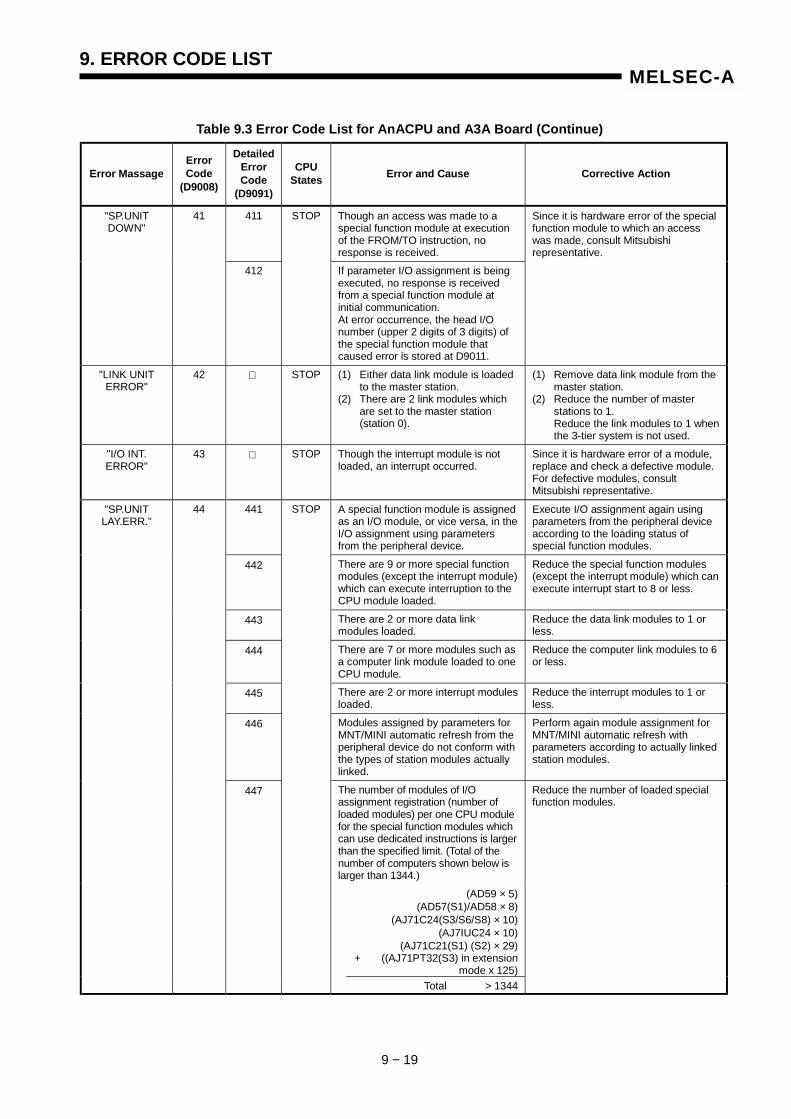
9. ERROR CODE LIST
9 − 19
MELSEC-A
Table 9.3 Error Code List for AnACPU and A3A Board (Continue)
Error MassageErrorCode
(D9008)
DetailedErrorCode
(D9091)
CPUStates Error and Cause Corrective Action
411 Though an access was made to aspecial function module at executionof the FROM/TO instruction, noresponse is received.
"SP.UNITDOWN"
41
412
STOP
If parameter I/O assignment is beingexecuted, no response is receivedfrom a special function module atinitial communication.At error occurrence, the head I/Onumber (upper 2 digits of 3 digits) ofthe special function module thatcaused error is stored at D9011.
Since it is hardware error of the specialfunction module to which an accesswas made, consult Mitsubishirepresentative.
"LINK UNITERROR"
42 STOP (1) Either data link module is loaded to the master station.
(2) There are 2 link modules which are set to the master station (station 0).
(1) Remove data link module from the master station.
(2) Reduce the number of master stations to 1.Reduce the link modules to 1 whenthe 3-tier system is not used.
"I/O INT.ERROR"
43 STOP Though the interrupt module is notloaded, an interrupt occurred.
Since it is hardware error of a module,replace and check a defective module.For defective modules, consultMitsubishi representative.
441 A special function module is assignedas an I/O module, or vice versa, in theI/O assignment using parametersfrom the peripheral device.
Execute I/O assignment again usingparameters from the peripheral deviceaccording to the loading status ofspecial function modules.
442 There are 9 or more special functionmodules (except the interrupt module)which can execute interruption to theCPU module loaded.
Reduce the special function modules(except the interrupt module) which canexecute interrupt start to 8 or less.
443 There are 2 or more data linkmodules loaded.
Reduce the data link modules to 1 orless.
444 There are 7 or more modules such asa computer link module loaded to oneCPU module.
Reduce the computer link modules to 6or less.
445 There are 2 or more interrupt modulesloaded.
Reduce the interrupt modules to 1 orless.
446 Modules assigned by parameters forMNT/MINI automatic refresh from theperipheral device do not conform withthe types of station modules actuallylinked.
Perform again module assignment forMNT/MINI automatic refresh withparameters according to actually linkedstation modules.
The number of modules of I/Oassignment registration (number ofloaded modules) per one CPU modulefor the special function modules whichcan use dedicated instructions is largerthan the specified limit. (Total of thenumber of computers shown below islarger than 1344.)
(AD59 × 5)(AD57(S1)/AD58 × 8)
(AJ71C24(S3/S6/S8) × 10)(AJ7IUC24 × 10)
(AJ71C21(S1) (S2) × 29)+ ((AJ71PT32(S3) in extension
mode x 125)
"SP.UNITLAY.ERR."
44
447
STOP
Total > 1344
Reduce the number of loaded specialfunction modules.

9. ERROR CODE LIST
9 − 20
MELSEC-A
Table 9.3 Error Code List for AnACPU and A3A Board (Continue)
Error MassageErrorCode
(D9008)
DetailedErrorCode
(D9091)
CPUStates Error and Cause Corrective Action
461 Module specified by the FROM / TO instruction is not a specialfunction module.
Read the error step using a peripheraldevice and check and correct contentsof the FROM / TO instruction of thestep.
"SP.UNITERROR"
(Checked atexecution of the
FROM/TOinstruction orthe dedicatedinstructions forspecial function
modules.)
46
462
Stop orContinue (set
bypara-
meter) Module specified by the dedicatedinstruction for special function moduleis not a special function module or nota corresponding special functionmodule.
Read the error step using a peripheraldevice and check and correct contentsof the dedicated instruction for specialfunction modules of the step.
"LINK PARA.ERROR"
47 Continue
(1) Data written to the parameter areas of the link of which range was set by parameters using a peripheral device does not conform with the data of link parameters read by the CPU.Or, link parameters are not written.
(2) Total number of local stations is set at 0.
(1) Write in parameters again and check.
(2) Check setting of station numbers.(3) If the same error indication is given
again, it is hardware failure. Consult Mitsubishi representative.
501 (1) When file registers (R) are used, operation is executed outside of specified ranges of device numbers and block numbers of file registers (R).
(2) File registers are used in the program without setting capacity of file registers.
502 Combination of the devices specifiedby instruction is incorrect.
503 Stored data or constant of specifieddevice is not in the usable range.
504 Set number of data to be handled isout of the usable range.
505 (1) Station number specified by the LEDA/ B LRDP LCDA/ B LWTP , LRDP , LWTP instructions is not a local station.
(2) Head I/O number specified bythe LEDA/ B RFRP LEDA/ B RTOP,
RFRP , RTOP instructions is not of a remote station.
506 Head I/O number specified by theLEDA/ B RFRP LEDA/ B RTOP, RFRP , RTOP instructions is not ofa special function module.
Read the error step using a peripheraldevice and check and correct programof the step.
"OPERATIONERROR"
(Checked atexecution ofinstruction.)
50
507
Stop orContinue (set
bypara-
meter)
(1) When the AD57(S1) or AD58 was executing instructions in divided processing mode, other instructions were executed to either of them.
(2) When an AD57(S1) or AD58 wasexecuting instructions in divided processing mode, other instructions were executed in divided mode to another AD57(S1) or AD58.
Read the error step using a peripheraldevice and provide interlock withspecial relay M9066 or modify programstructure so that, when the AD57(S1) orAD58 is executing instructions individed processing mode, otherinstructions may not be executed toeither of them or to another AD57(S1)or AD58 in divided mode.

9. ERROR CODE LIST
9 − 21
MELSEC-A
Table 9.3 Error Code List for AnACPU and A3A Board (Continue)
Error MassageErrorCode
(D9008)
DetailedErrorCode
(D9091)
CPUStates Error and Cause Corrective Action
"OPERATIONERROR"
(Checked atexecution ofinstruction.)
50 509 STOP (1) An instruction which cannot be executed by remote terminal modules connected to the MNET/MINI-S3 was executed to the modules.
(2) When the PRC instruction was executed to a remote terminal, the communication request registration areas overflowed.
(3) The PIDCONT instruction was executed without executing the PIDINIT instruction.The PID57 instruction was executed without executing the PIDINIT or PIDCONT instruction.
(1) Read the error step using a peripheral device and correct the program, meeting loaded conditions of remote terminal modules.
(2) Provide interlock using M9081 (communication request registration areas BUSY signal) or D9081 (number of vacant areas in the communication request registration areas) when the PRC instruction is executed to a remote terminal.
(3) Execute the PIDCONT instructionafter execution of the PIDINIT instruction.Execute the PID57 instruction after execution of the PIDINIT and PIDCONT instructions.
(1) The CPU malfunctioned due to noise.
(2) Hardware failure.
(1) Take proper countermeasures for noise.
(2) Hardware failure.
"MAIN CPUDOWN"
60
602
STOP
(1) Failure in the power module, CPU module, main base unit or expansion cable is detected.
(1) Replace the power module, CPU module, main base unit or expansion cable.
"BATTERYERROR"
(Checked atpower on.)
70 Continue
(1) Battery voltage has lowered below specified level.
(2) Battery lead connector is not connected.
(1) Replace battery.(2) If a RAM memory or power failure
compensation function is used, connect the lead connector.

9. ERROR CODE LIST
9 − 22
MELSEC-A
9.5 Error Code List for the AnUCPU, A2ASCPU and A2USH board
Table 9.4 shows the error messages, error codes, description and cause of errorand corrective actions of detailed error codes. (*: The detailed error codes added toAnUCPU, A2ASCPU and A2USH board)Error codes, detailed error codes and error steps are stored in the following specialregisters.
Error code: D9008Detailed error code: D9091Error step: D9010 and D9011
Table 9.4 Error Code List for the AnU, A2AS and A2USH board
Error MassageErrorCode
(D9008)
DetailedErrorCode
(D9091)
CPUStates Error and Cause Corrective Action
101 Instruction codes which the CPUcannot decode are included in theprogram.
(1) Read the error step using a peripheral device and correct the program of the step.
(2) Check the ROM if it contains instruction codes which cannot be decoded. If it does, replace it witha correct ROM.
102 Index qualification is specified for a32-bit constant.
103 Device specified by a dedicatedinstruction is not correct.
104 An dedicated instruction has incorrectprogram structure.
105 An dedicated instruction has incorrectcommand name.
106 Index qualification using Z or V isincluded in the program betweenLEDA/ B IX and LEDA/B IXEND.
107 (1) Index qualification is specified forthe device numbers and set values in the OUT instruction oftimers and counters.
(2) Index qualification is specified at the label number of the pointer (P) provided to the head of destination of the CJ , SCJ , CALL , CALLP , JMP , LEDA/B , FCALL and LEDA/B , BREAK instructions or at the label number of the interrupt pointer (I) provided to the head of an interrupt program.
"INSTRCTCODE ERR"
(Checked whenSTOP → RUNor at executionof instruction.)
10
108
STOP
Errors other than 101 to 107mentioned above.
Read the error step using a peripheraldevice and correct the program of thestep.

9. ERROR CODE LIST
9 − 23
MELSEC-A
Table 9.4 Error Code List for the AnU, A2AS and A2USH board (Continue)
Error MassageErrorCode
(D9008)
DetailedErrorCode
(D9091)
CPUStates Error and Cause Corrective Action
111 Capacity settings of the main and subprograms, microcomputer program,file register comments, status latch,sampl-ing trace and extension fileregisters are not within the usablerange of the CPU.
112 Total of the set capacity of the mainand sub programs, file registercomments, status latch, samplingtrace and extension file registersexceeds capacity of the memorycassette.
Read parameters in the CPU memory,check the contents, make necessarycorrections and write them again to thememory.
113 Latch range set by parameters orsetting of M, L or S is incorrect.
114 Sum check error
115 Either of settings of the remote RUN/PAUSE contact point by parameters,operation mode at occurrence oferror, annunciator indication mode, orSTOP → RUN indication mode isincorrect.
116 The MNET-MINI automatic refreshsetting by parameters is incorrect.
117 Timer setting by parameters isincorrect.
"PARAMETERERROR"
(Checked atpower on and atSTOP/PAUSE
→ RUN.)
11
118
STOP
Counter setting by parameters isincorrect.
Read parameters in the CPU memory,check the contents, make necessarycorrections and write them again to thememory
121 The END ( FEND ) instruction is notgiven in the main program.
Write the END instruction at the endof the main program.
122 The END ( FEND ) instruction is notgiven in the sub program if the subprogram is set by parameters.
123 (1) When subprogram 2 is set by a parameter, there is no END(FEND) instruction in subprogram 2.
(2) When subprogram 2 is set by a parameter, subprogram 2 has notbeen written from a peripheral device.
"MISSING ENDINS"
(Checked atSTOP → RUN.)
12
124
STOP
(1) When subprogram 3 is set by a parameter, there is no END(FEND) instruction in subprogram 3.
(2) When subprogram 3 is set by a parameter, subprogram 2 has notbeen written from a peripheral device.
Write the END instruction at the endof the sub program.
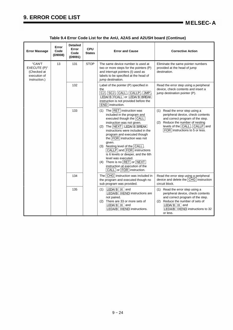
9. ERROR CODE LIST
9 − 24
MELSEC-A
Table 9.4 Error Code List for the AnU, A2AS and A2USH board (Continue)
Error MassageErrorCode
(D9008)
DetailedErrorCode
(D9091)
CPUStates Error and Cause Corrective Action
131 The same device number is used attwo or more steps for the pointers (P)and interrupt pointers (I) used aslabels to be specified at the head ofjump destination.
Eliminate the same pointer numbersprovided at the head of jumpdestination.
132 Label of the pointer (P) specified inthe CJ , SCJ , CALL , CALLP , JMP ,LEDA/ B FCALL or LEDA/ B BREAKinstruction is not provided before the END instruction.
Read the error step using a peripheraldevice, check contents and insert ajump destination pointer (P).
133 (1) The RET instruction was included in the program and executed though the CALL instruction was not given.
(2) The NEXT LEDA/ B BREAKinstructions were included in the program and executed though the FOR instruction was not given.
(3) Nesting level of the CALL , CALLP and FOR instructions is 6 levels or deeper, and the 6th level was executed.
(4) There is no RET or NEXT instruction at execution of the CALL or FOR instruction.
(1) Read the error step using a peripheral device, check contents and correct program of the step.
(2) Reduce the number of nesting levels of the CALL , CALLP and FOR instructions to 5 or less.
134 The CHG instruction was included inthe program and executed though nosub program was provided.
Read the error step using a peripheraldevice and delete the CHG instructioncircuit block.
"CAN'TEXECUTE (P)"
(Checked atexecution ofinstruction.)
13
135
STOP
(1) LEDA/ B IX and LEDA/B IXEND instructions arenot paired.
(2) There are 33 or more sets ofLEDA/ B IX and LEDA/B IXEND instructions.
(1) Read the error step using a peripheral device, check contents and correct program of the step.
(2) Reduce the number of sets ofLEDA/ B IX and LEDA/B IXEND instructions to 32or less.

9. ERROR CODE LIST
9 − 25
MELSEC-A
Table 9.4 Error Code List for the AnU, A2AS and A2USH board (Continue)
Error MassageErrorCode
(D9008)
DetailedErrorCode
(D9091)
CPUStates Error and Cause Corrective Action
141 Instructions (including NOP ) otherthan LDX , LDIX , ANDX and ANIX are included in the CHKinstruction circuit block.
142 Multiple CHK instructions are given.
143 The number of contact points in the CHK instruction circuit blockexceeds 150.
144 The LEDA CHK instructions are notpaired with the LEDA CHKENDinstructions, or 2 or more pairs ofthem are given.
145 Format of the block shown below,which is provided before the CHKinstruction circuit block, is not asspecified.
CJP254 P
146 Device number of D1 in theCHK D1 D2 instruction is differentfrom that of the contact point beforethe CJ P instruction.
147 Index qualification is used in thecheck pattern circuit.
"CHK FORMATERR"
(Checked atSTOP/PAUSE
→ RUN.)
14
148
STOP
(1) Multiple check pattern circuits of the LEDA CHK - LEDA CHKENDinstructions are given.
(2) There are 7 or more check condition circuits in theLEDA CHK - LEDA CHKENDinstructions.
(3) The check condition circuits in the LEDA CHK - LEDA CHKENDinstructions are written without using X and Y contact instructions or compare instructions.
(4) The check pattern circuits of the LEDA CHK - LEDA CHKENDinstructions are written with 257 or more steps.
Check the program of the CHKinstruction and correct it referring tocontents of detailed error codes.
151 The IRET instruction was givenoutside of the interrupt program andwas executed.
Read the error step using a peripheraldevice and delete the IRET instruction.
152 There is no IRET instruction in theinterrupt program.
Check the interrupt program if the IRET instruction is given in it.Write the IRET instruction if it is notgiven.
"CAN'TEXECUTE (I)"(Checked at
occurrence ofinterrupt.)
15
153
STOP
Though an interrupt module is used,no interrupt pointer (I) whichcorresponds to the module is given inthe program. Upon occurrence oferror, the problem pointer (I) numberis stored at D9011.
Monitor special register D9011 using aperipheral device, and check if theinterrupt program that corresponds tothe stored data is provided or if two ormore interrupt pointers (I) of the samenumber are given. Make necessarycorrections.

9. ERROR CODE LIST
9 − 26
MELSEC-A
Table 9.4 Error Code List for the AnU, A2AS and A2USH board (Continue)
Error MassageErrorCode
(D9008)
DetailedErrorCode
(D9091)
CPUStates Error and Cause Corrective Action
"CASSETTEERROR"
16 STOP Memory cassette is not loaded. Turn off the PC power and load thememory cassette.
201 The sequence program storage RAMin the CPU module caused an error.
202 The work area RAM in the CPUmodule caused an error.
203 The device memory in the CPUmodule caused an error.
"RAM ERROR"(Checked atpower on.)
20
204
STOP
The address RAM in the CPU modulecaused an error.
Since this is CPU hardware error,consult Mitsubishi representative.
211 The operation circuit for indexqualification in the CPU does not workcorrectly.
212 Hardware (logic) in the CPU does notoperate correctly.
"OPE CIRCUITERROR"
(Checked atpower on.)
213 The operation circuit for sequentialprocessing in the CPU does notoperate correctly.
214 In the END processing check, theoperation circuit for index qualificationin the CPU does not work correctly.
"OPE. CIRCUITERR."
(Checked atexecution of the
ENDinstruction)
21
215
STOP
In the END processing check, thehardware in the CPU does notoperate correctly.
Since this is CPU hardware error,consult Mitsubishi representative.
"WDT ERROR"(Checked atexecution of
ENDprocessing.)
22 STOP Scan time is longer than the WDTtime.(1) Scan time of the user's program
has been extended due to certainconditions.
(2) Scan time has been extended due to momentary power failure occurred during scanning.
(1) Calculate and check the scan time of user program and reduce the scan time using the CJ instruction or the like.
(2) Monitor contents of special registerD9005 using a peripheral device.If the contents are other than 0, power supply voltage may not be stable. Check power supply and reduce variation in voltage.
"END NOTEXECUTE"(Checked at
execution of theEND
instruction.)
24 241 STOP Whole program of specified programcapacity was executed withoutexecuting the END instructions.(1) When the END instruction was
to be executed, the instruction was read as other instruction code due to noise.
(2) The END instruction changed toother instruction code due to unknown cause.
(1) Reset and run the CPU again. If the same error recurs,Since this is CPU hardware error, consult Mitsubishi representative.
"MAIN CPUDOWN"
26 STOP The main CPU is malfunctioning orfaulty.
Since this is CPU hardware error,consult Mitsubishi representative
"UNIT VERIFYERR"
(Checkedcontinuously.)
31 Stop orContinue (set
bypara-
meter)
Current I/O module information isdifferent from that recognized whenthe power was turned on.(1) The I/O module (including special
function modules) connection became loose or the module wasdisconnected during operation, orwrong module was connected.
Read detailed error code using aperipheral device and check or replacethe module which corresponds to thedata (I/O head number).Or, monitor special registers D9116 toD9123 using a peripheral device andcheck or replace the modules ifcorresponding data bit is "1".
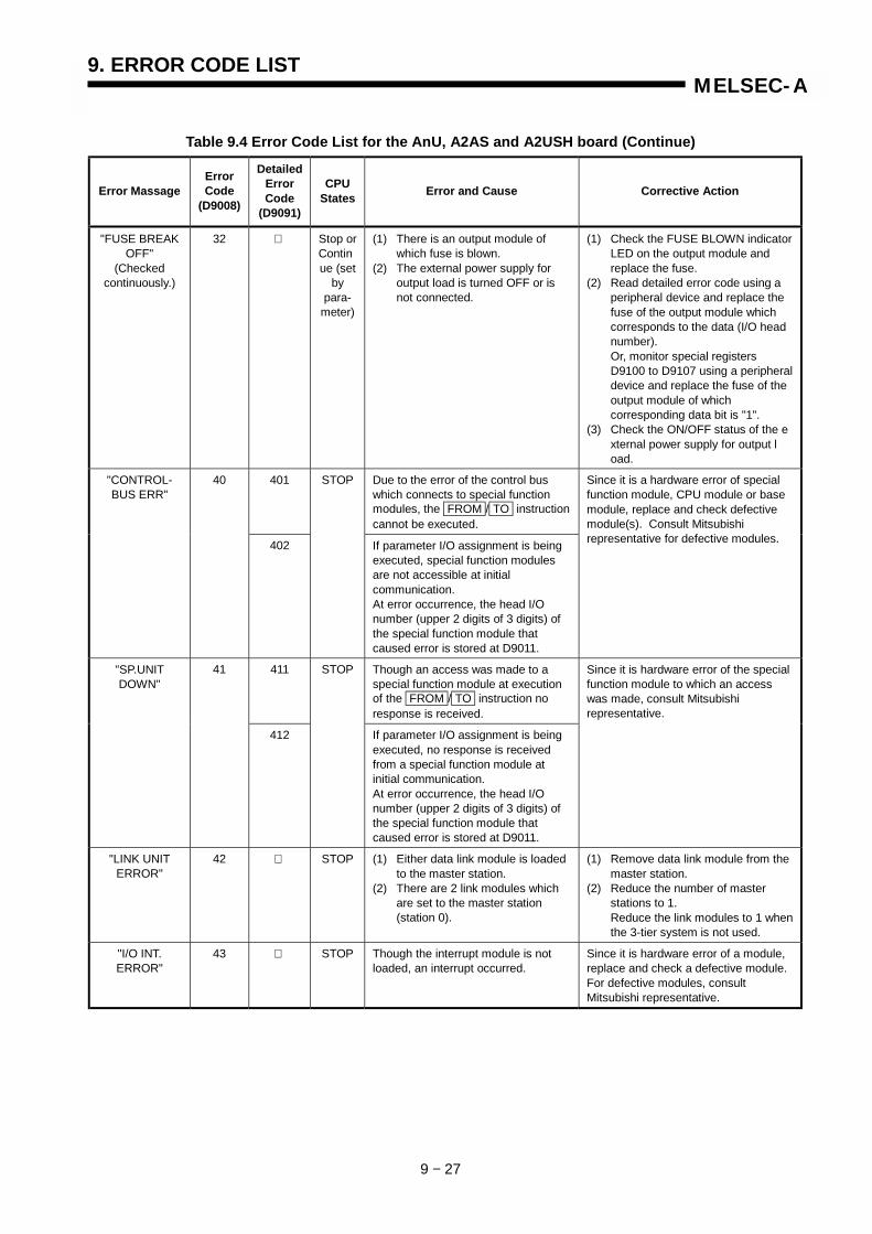
9. ERROR CODE LIST
9 − 27
MELSEC-A
Table 9.4 Error Code List for the AnU, A2AS and A2USH board (Continue)
Error MassageErrorCode
(D9008)
DetailedErrorCode
(D9091)
CPUStates Error and Cause Corrective Action
"FUSE BREAKOFF"
(Checkedcontinuously.)
32 Stop orContinue (set
bypara-
meter)
(1) There is an output module of which fuse is blown.
(2) The external power supply for output load is turned OFF or is not connected.
(1) Check the FUSE BLOWN indicatorLED on the output module and replace the fuse.
(2) Read detailed error code using a peripheral device and replace the fuse of the output module which corresponds to the data (I/O head number).Or, monitor special registers D9100 to D9107 using a peripheraldevice and replace the fuse of the output module of which corresponding data bit is "1".
(3) Check the ON/OFF status of the external power supply for output load.
401 Due to the error of the control buswhich connects to special functionmodules, the FROM / TO instructioncannot be executed.
"CONTROL-BUS ERR"
40
402
STOP
If parameter I/O assignment is beingexecuted, special function modulesare not accessible at initialcommunication.At error occurrence, the head I/Onumber (upper 2 digits of 3 digits) ofthe special function module thatcaused error is stored at D9011.
Since it is a hardware error of specialfunction module, CPU module or basemodule, replace and check defectivemodule(s). Consult Mitsubishirepresentative for defective modules.
411 Though an access was made to aspecial function module at executionof the FROM / TO instruction noresponse is received.
"SP.UNITDOWN"
41
412
STOP
If parameter I/O assignment is beingexecuted, no response is receivedfrom a special function module atinitial communication.At error occurrence, the head I/Onumber (upper 2 digits of 3 digits) ofthe special function module thatcaused error is stored at D9011.
Since it is hardware error of the specialfunction module to which an accesswas made, consult Mitsubishirepresentative.
"LINK UNITERROR"
42 STOP (1) Either data link module is loaded to the master station.
(2) There are 2 link modules which are set to the master station (station 0).
(1) Remove data link module from the master station.
(2) Reduce the number of master stations to 1.Reduce the link modules to 1 whenthe 3-tier system is not used.
"I/O INT.ERROR"
43 STOP Though the interrupt module is notloaded, an interrupt occurred.
Since it is hardware error of a module,replace and check a defective module.For defective modules, consultMitsubishi representative.
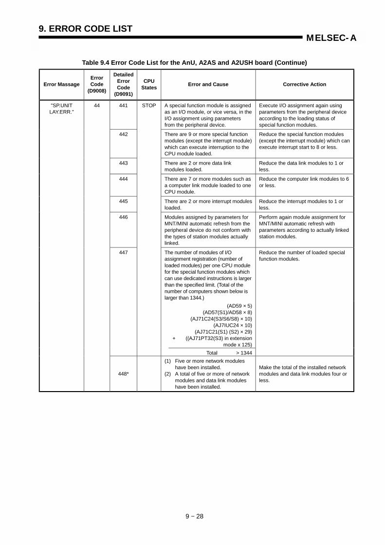
9. ERROR CODE LIST
9 − 28
MELSEC-A
Table 9.4 Error Code List for the AnU, A2AS and A2USH board (Continue)
Error MassageErrorCode
(D9008)
DetailedErrorCode
(D9091)
CPUStates Error and Cause Corrective Action
441 A special function module is assignedas an I/O module, or vice versa, in theI/O assignment using parametersfrom the peripheral device.
Execute I/O assignment again usingparameters from the peripheral deviceaccording to the loading status ofspecial function modules.
442 There are 9 or more special functionmodules (except the interrupt module)which can execute interruption to theCPU module loaded.
Reduce the special function modules(except the interrupt module) which canexecute interrupt start to 8 or less.
443 There are 2 or more data linkmodules loaded.
Reduce the data link modules to 1 orless.
444 There are 7 or more modules such asa computer link module loaded to oneCPU module.
Reduce the computer link modules to 6or less.
445 There are 2 or more interrupt modulesloaded.
Reduce the interrupt modules to 1 orless.
446 Modules assigned by parameters forMNT/MINI automatic refresh from theperipheral device do not conform withthe types of station modules actuallylinked.
Perform again module assignment forMNT/MINI automatic refresh withparameters according to actually linkedstation modules.
The number of modules of I/Oassignment registration (number ofloaded modules) per one CPU modulefor the special function modules whichcan use dedicated instructions is largerthan the specified limit. (Total of thenumber of computers shown below islarger than 1344.)
(AD59 × 5)(AD57(S1)/AD58 × 8)
(AJ71C24(S3/S6/S8) × 10)(AJ7IUC24 × 10)
(AJ71C21(S1) (S2) × 29)+ ((AJ71PT32(S3) in extension
mode x 125)
447
STOP
Total > 1344
Reduce the number of loaded specialfunction modules.
"SP.UNITLAY.ERR."
44
448*
(1) Five or more network modules have been installed.
(2) A total of five or more of network modules and data link modules have been installed.
Make the total of the installed networkmodules and data link modules four orless.

9. ERROR CODE LIST
9 − 29
MELSEC-A
Table 9.4 Error Code List for the AnU, A2AS and A2USH board (Continue)
Error MassageErrorCode
(D9008)
DetailedErrorCode
(D9091)
CPUStates Error and Cause Corrective Action
461 Module specified by the FROM / TO instruction is not a specialfunction module.
Read the error step using a peripheraldevice and check and correct contentsof the FROM / TO instruction of thestep.
"SP.UNITERROR"
(Checked atexecution of the
FROM/TOinstruction orthe dedicatedinstructions forspecial function
modules.)
46
462
Stop orContinue (set
bypara-
meter) (1) Module specified by the dedicated instruction for special function module is not a special function module or not a corresponding special function module.
(2) A command was issued to a CC-Link module with function versionunder B.
(3) A CC-Link dedicated command was issued to a CC-Link module for which the network parametershave not been set.
(1) Read the error step using a peripheral device and check and correct contents of the dedicated instruction for special function modules of the step.
(2) Replace with a CC-Link module having function version B and above.
(3) Set the parameters.
0 [When using MELSECNET/(II)](1) When the link range at a data link
CPU which is also a master station (station number = 00) is set by parameter setting at a peripheral device, for some reason the data written to the linkparameter area differs from the link parameter data read by the CPU. Alternatively, no link parameters have been written.
(2) The total number of slave stations is set at 0.
(1) Write the parameters again and check.
(2) Check the station number settings.(3) Persistent error occurrence may
indicate a hardware fault. Consult your nearest Mitsubishi representative, explaining the nature of the problem.
470* [When using MELSECNET/10](1) The contents of the network
refresh parameters written from aperipheral device differ from the actual system at the base unit.
(2) The network refresh parameters have not been written.
Write the network refresh parametersagain and check.
471* [When using MELSECNET/10](1) The transfer source device range
and transfer destination device range specified for the inter-network transfer parameters are in the same network.
(2) The specified range of transfer source devices or transfer destination devices for the inter-network transfer parameters spans two or more networks.
(3) The specified range of transfer source devices or transfer destination devices for the inter-network transfer parameters is not used by the network.
Write the network parameters againand check.
"LINK PARA.ERROR"
47
472*
Continue
[When using MELSECNET/10]The contents of the routingparameters written from a peripheraldevice differ from the actual networksystem.
Write the routing parameters again andcheck.

9. ERROR CODE LIST
9 − 30
MELSEC-A
Table 9.4 Error Code List for the AnU, A2AS and A2USH board (Continue)
Error MassageErrorCode
(D9008)
DetailedErrorCode
(D9091)
CPUStates Error and Cause Corrective Action
473* [When using MELSECNET/10](1) The contents of the network
parameters for the first link unit, written from a peripheral device, differ from the actual network system.
(2) The link parameters for the first link unit have not been written.
(3) The setting for the total number of stations is 0.
474* [When using MELSECNET/10](1) The contents of the network
parameters for the second link unit, written from a peripheral device, differ from the actual network system.
(2) The link parameters for the second link unit have not been written.
(3) The setting for the total number of stations is 0.
475* [When using MELSECNET/10](1) The contents of the network
parameters for the third link unit, written from a peripheral device, differ from the actual network system.
(2) The link parameters for the third link unit have not been written.
(3) The setting for the total number of stations is 0.
476* [When using MELSECNET/10](1) The contents of the network
parameters for the fourth link unit, written from a peripheral device, differ from the actual network system.
(2) The link parameters for the fourthlink unit have not been written.
(3) The setting for the total number of stations is 0.
(1) Write the parameters again and check.
(2) Check the station number settings.(3) Persistent error occurrence may
indicate a hardware fault. Consult your nearest Mitsubishi representative, explaining the nature of the problem.
"LINK PARA.ERROR"
47
477
Continue
A ink parameter error was detectedby the CC-Link module.
(1) Write the parameters in again andcheck.
(2) If the error appears again, there isa problem with the hardware.Consult your nearest SystemService, sales office or branchoffice.
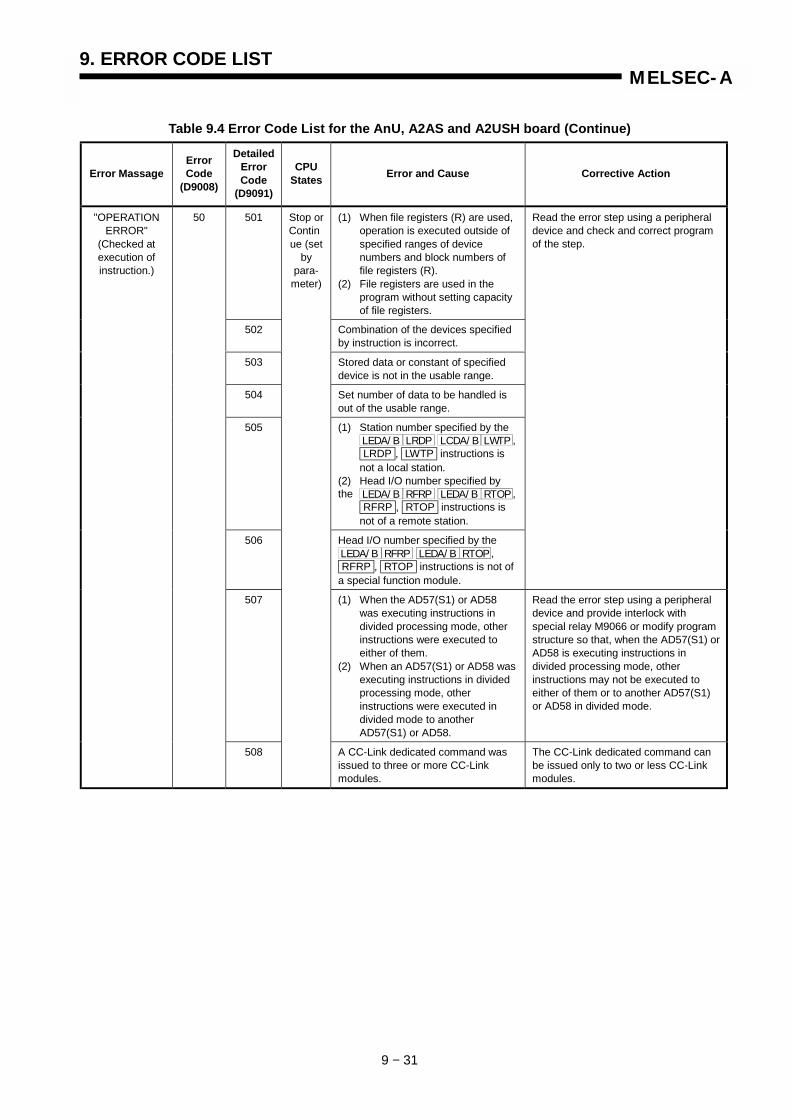
9. ERROR CODE LIST
9 − 31
MELSEC-A
Table 9.4 Error Code List for the AnU, A2AS and A2USH board (Continue)
Error MassageErrorCode
(D9008)
DetailedErrorCode
(D9091)
CPUStates Error and Cause Corrective Action
501 (1) When file registers (R) are used, operation is executed outside of specified ranges of device numbers and block numbers of file registers (R).
(2) File registers are used in the program without setting capacity of file registers.
502 Combination of the devices specifiedby instruction is incorrect.
503 Stored data or constant of specifieddevice is not in the usable range.
504 Set number of data to be handled isout of the usable range.
505 (1) Station number specified by the LEDA/ B LRDP LCDA/ B LWTP , LRDP , LWTP instructions is not a local station.
(2) Head I/O number specified bythe LEDA/ B RFRP LEDA/ B RTOP,
RFRP , RTOP instructions is not of a remote station.
506 Head I/O number specified by theLEDA/ B RFRP LEDA/ B RTOP, RFRP , RTOP instructions is not ofa special function module.
Read the error step using a peripheraldevice and check and correct programof the step.
507 (1) When the AD57(S1) or AD58 was executing instructions in divided processing mode, other instructions were executed to either of them.
(2) When an AD57(S1) or AD58 wasexecuting instructions in divided processing mode, other instructions were executed in divided mode to another AD57(S1) or AD58.
Read the error step using a peripheraldevice and provide interlock withspecial relay M9066 or modify programstructure so that, when the AD57(S1) orAD58 is executing instructions individed processing mode, otherinstructions may not be executed toeither of them or to another AD57(S1)or AD58 in divided mode.
"OPERATIONERROR"
(Checked atexecution ofinstruction.)
50
508
Stop orContinue (set
bypara-
meter)
A CC-Link dedicated command wasissued to three or more CC-Linkmodules.
The CC-Link dedicated command canbe issued only to two or less CC-Linkmodules.
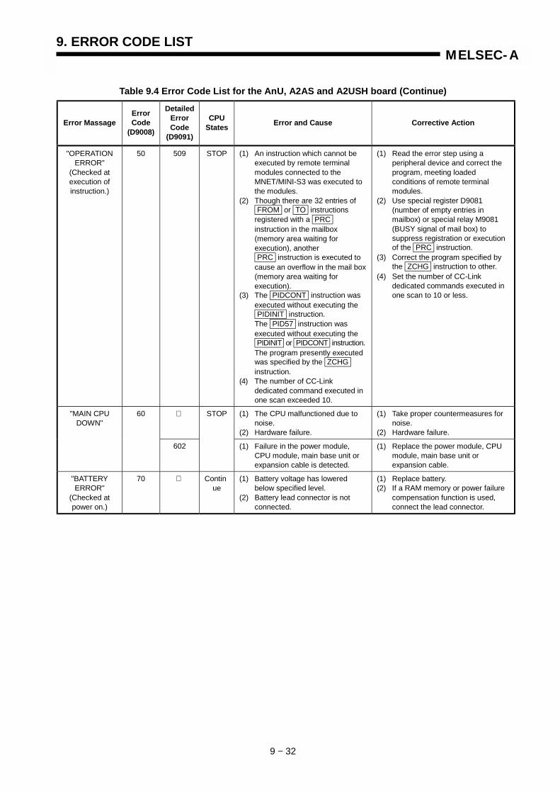
9. ERROR CODE LIST
9 − 32
MELSEC-A
Table 9.4 Error Code List for the AnU, A2AS and A2USH board (Continue)
Error MassageErrorCode
(D9008)
DetailedErrorCode
(D9091)
CPUStates Error and Cause Corrective Action
"OPERATIONERROR"
(Checked atexecution ofinstruction.)
50 509 STOP (1) An instruction which cannot be executed by remote terminal modules connected to the MNET/MINI-S3 was executed to the modules.
(2) Though there are 32 entries of FROM or TO instructions registered with a PRC instruction in the mailbox (memory area waiting for execution), another PRC instruction is executed to cause an overflow in the mail box(memory area waiting for execution).
(3) The PIDCONT instruction was executed without executing the PIDINIT instruction.The PID57 instruction was executed without executing the PIDINIT or PIDCONT instruction.The program presently executed was specified by the ZCHG instruction.
(4) The number of CC-Link dedicated command executed in one scan exceeded 10.
(1) Read the error step using a peripheral device and correct the program, meeting loaded conditions of remote terminal modules.
(2) Use special register D9081 (number of empty entries in mailbox) or special relay M9081 (BUSY signal of mail box) to suppress registration or execution of the PRC instruction.
(3) Correct the program specified by the ZCHG instruction to other.
(4) Set the number of CC-Link dedicated commands executed in one scan to 10 or less.
(1) The CPU malfunctioned due to noise.
(2) Hardware failure.
(1) Take proper countermeasures for noise.
(2) Hardware failure.
"MAIN CPUDOWN"
60
602
STOP
(1) Failure in the power module, CPU module, main base unit or expansion cable is detected.
(1) Replace the power module, CPU module, main base unit or expansion cable.
"BATTERYERROR"
(Checked atpower on.)
70 Continue
(1) Battery voltage has lowered below specified level.
(2) Battery lead connector is not connected.
(1) Replace battery.(2) If a RAM memory or power failure
compensation function is used, connect the lead connector.

9. ERROR CODE LIST
9 − 33
MELSEC-A
9.6 Error Code List for the QCPU-A (A Mode)
Meanings and causes of error message, error codes, detailed error codes andcorrective actions are described.
Table 9.5 Error Code List for the QCPU-A (A Mode)
Error MassageErrorCode
(D9008)
DetailedErrorCode
(D9091)
CPUStates Error and Cause Corrective Action
101 Instruction codes which the CPUmodule cannot decode are included inthe program.
(1) Read the error step using aperipheral device and correct theprogram of the step.
(2) Check the ROM if it containsinstruction codes which cannot bedecoded. If it does, replace it with acorrect ROM.
102 Index qualification is specified for a 32-bit constant.
103 Device specified by a dedicatedinstruction is not correct.
104 A dedicated instruction has incorrectprogram structure.
105 A dedicated instruction has incorrectcommand name.
106 Index qualification using Z or V isincluded in the program betweenLEDA/ B IX and LEDA/B IXEND.
107 (1) Index qualification is specified forthe device numbers and set valuesin the OUT instruction of timers andcounters.
(2) Index qualification is specified atthe label number of the pointer (P)provided to the head of destinationof the CJ , SCJ , CALL , CALLP, JMP , LEDA/ B FCALL andLEDA/ B BREAK instructions or atthe label number of the interruptpointer (I) provided to the head ofan interrupt program.
"INSTRCTCODE ERR"(Checked whenSTOP RUNor at executionof instruction.)
10
108
STOP
Errors other than 101 to 107mentioned above.
Read the error step using a peripheraldevice and correct the program of thestep.
111 Capacity settings of the main and subprograms, microcomputer program, fileregister comments, status latch,sampling trace and extension fileregisters are not within the usablerange of the CPU.
112 Total of the set capacity of the mainand sub programs, file registercomments, status latch, sampling traceand extension file registers exceedscapacity of the memory cassette.
113 Latch range set by parameters orsetting of M, L or S is incorrect.
"PARAMETERERROR"(Checked atpower on and atSTOP/PAUSE
RUN.)
11
114
STOP
Sum check error
Read parameters in the CPU memory,check the contents, make necessarycorrections and write them again to thememory.
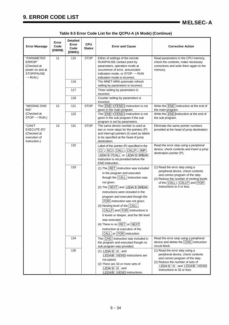
9. ERROR CODE LIST
9 − 34
MELSEC-A
Table 9.5 Error Code List for the QCPU-A (A Mode) (Continue)
Error MassageErrorCode
(D9008)
DetailedErrorCode
(D9091)
CPUStates Error and Cause Corrective Action
115 Either of settings of the remoteRUN/PAUSE contact point byparameters, operation mode atoccurrence of error, annunciatorindication mode, or STOP RUNindication mode is incorrect.
116 The MNET-MINI automatic refreshsetting by parameters is incorrect.
117 Timer setting by parameters isincorrect.
"PARAMETERERROR"(Checked atpower on and atSTOP/PAUSE
RUN.)
11
118
STOP
Counter setting by parameters isincorrect.
Read parameters in the CPU memory,check the contents, make necessarycorrections and write them again to thememory.
121 The END ( FEND ) instruction is notgiven in the main program.
Write the END instruction at the end ofthe main program.
"MISSING ENDINS"(Checked atSTOP RUN.)
12
122
STOP
The END ( FEND ) instruction is notgiven in the sub program if the subprogram is set by parameters.
Write the END instruction at the end ofthe sub program.
131 The same device number is used attwo or more steps for the pointers (P)and interrupt pointers (I) used as labelsto be specified at the head of jumpdestination.
Eliminate the same pointer numbersprovided at the head of jump destination.
132 Label of the pointer (P) specified in the CJ , SCJ , CALL , CALLP , JMP ,LEDA/ B FCALL or LEDA/ B BREAKinstruction is not provided before theEND instruction.
Read the error step using a peripheraldevice, check contents and insert a jumpdestination pointer (P).
133 (1) The RET instruction was includedin the program and executedthough the CALL instruction wasnot given.
(2) The NEXT and LEDA/ B BREAKinstructions were included in theprogram and executed though the FOR instruction was not given.
(3) Nesting level of the CALL , CALLP and FOR instructions is6 levels or deeper, and the 6th levelwas executed.
(4) There is no RET or NEXTinstruction at execution of the CALL or FOR instruction.
(1) Read the error step using aperipheral device, check contentsand correct program of the step.
(2) Reduce the number of nesting levelsof the CALL , CALLP and FOR instructions to 5 or less.
134 The CHG instruction was included inthe program and executed though nosub program was provided.
Read the error step using a peripheraldevice and delete the CHG instructioncircuit block.
"CAN'TEXECUTE (P)"(Checked atexecution ofinstruction.)
13
135
STOP
(1) LEDA/ B IX andLEDA/B IXEND instructions arenot paired.
(2) There are 33 or more sets ofLEDA/ B IX andLEDA/B IXEND instructions.
(1) Read the error step using aperipheral device, check contentsand correct program of the step.
(2) Reduce the number of sets ofLEDA/ B IX and LEDA/B IXENDinstructions to 32 or less.
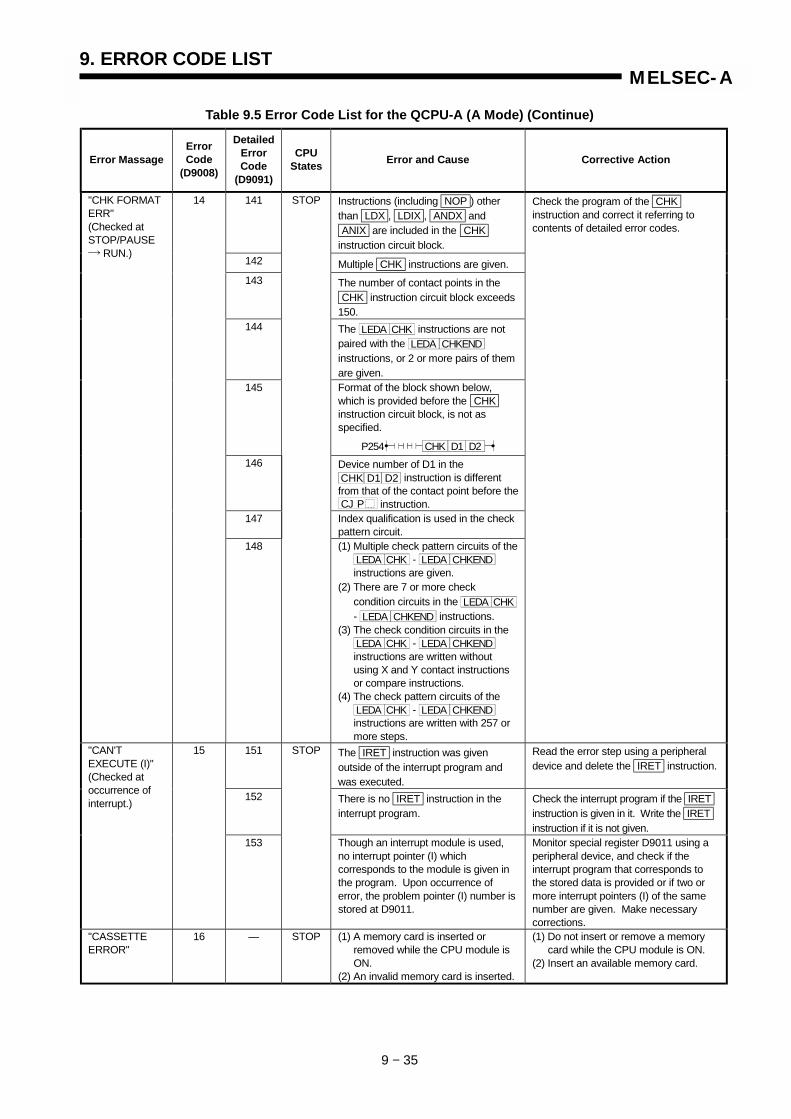
9. ERROR CODE LIST
9 − 35
MELSEC-A
Table 9.5 Error Code List for the QCPU-A (A Mode) (Continue)
Error MassageErrorCode
(D9008)
DetailedErrorCode
(D9091)
CPUStates Error and Cause Corrective Action
141 Instructions (including NOP ) otherthan LDX , LDIX , ANDX and ANIX are included in the CHK instruction circuit block.
142 Multiple CHK instructions are given.143 The number of contact points in the
CHK instruction circuit block exceeds150.
144 The LEDA CHK instructions are notpaired with the LEDA CHKENDinstructions, or 2 or more pairs of themare given.
145 Format of the block shown below,which is provided before the CHK instruction circuit block, is not asspecified.
CHKP254 D1 D2146 Device number of D1 in the
CHK D1 D2 instruction is differentfrom that of the contact point before theCJ P instruction.
147 Index qualification is used in the checkpattern circuit.
"CHK FORMATERR"(Checked atSTOP/PAUSE
RUN.)
14
148
STOP
(1) Multiple check pattern circuits of theLEDA CHK - LEDA CHKENDinstructions are given.
(2) There are 7 or more checkcondition circuits in the LEDA CHK- LEDA CHKEND instructions.
(3) The check condition circuits in theLEDA CHK - LEDA CHKENDinstructions are written withoutusing X and Y contact instructionsor compare instructions.
(4) The check pattern circuits of theLEDA CHK - LEDA CHKENDinstructions are written with 257 ormore steps.
Check the program of the CHK instruction and correct it referring tocontents of detailed error codes.
151 The IRET instruction was givenoutside of the interrupt program andwas executed.
Read the error step using a peripheraldevice and delete the IRET instruction.
152 There is no IRET instruction in theinterrupt program.
Check the interrupt program if the IRET instruction is given in it. Write the IRET instruction if it is not given.
"CAN'TEXECUTE (I)"(Checked atoccurrence ofinterrupt.)
15
153
STOP
Though an interrupt module is used,no interrupt pointer (I) whichcorresponds to the module is given inthe program. Upon occurrence oferror, the problem pointer (I) number isstored at D9011.
Monitor special register D9011 using aperipheral device, and check if theinterrupt program that corresponds tothe stored data is provided or if two ormore interrupt pointers (I) of the samenumber are given. Make necessarycorrections.
"CASSETTEERROR"
16 — STOP (1) A memory card is inserted orremoved while the CPU module isON.
(2) An invalid memory card is inserted.
(1) Do not insert or remove a memorycard while the CPU module is ON.
(2) Insert an available memory card.
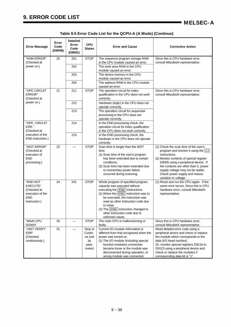
9. ERROR CODE LIST
9 − 36
MELSEC-A
Table 9.5 Error Code List for the QCPU-A (A Mode) (Continue)
Error MassageErrorCode
(D9008)
DetailedErrorCode
(D9091)
CPUStates Error and Cause Corrective Action
201 The sequence program storage RAMin the CPU module caused an error.
202 The work area RAM in the CPUmodule caused an error.
203 The device memory in the CPUmodule caused an error.
"RAM ERROR"(Checked atpower on.)
20
204
STOP
The address RAM in the CPU modulecaused an error.
Since this is CPU hardware error,consult Mitsubishi representative.
211 The operation circuit for indexqualification in the CPU does not workcorrectly.
212 Hardware (logic) in the CPU does notoperate correctly.
"OPE CIRCUITERROR"(Checked atpower on.)
213 The operation circuit for sequentialprocessing in the CPU does notoperate correctly.
214 In the END processing check, theoperation circuit for index qualificationin the CPU does not work correctly.
"OPE. CIRCUITERR."(Checked atexecution of theEND instruction.)
21
215
STOP
In the END processing check, thehardware in the CPU does not operatecorrectly.
Since this is CPU hardware error,consult Mitsubishi representative.
"WDT ERROR"(Checked atexecution ofENDprocessing.)
22 — STOP Scan time is longer than the WDTtime.(1) Scan time of the user's program
has been extended due to certainconditions.
(2) Scan time has been extended dueto momentary power failureoccurred during scanning.
(1) Check the scan time of the user'sprogram and shorten it using the CJ instructions.
(2) Monitor contents of special registerD9005 using a peripheral device. Ifthe contents are other than 0, powersupply voltage may not be stable.Check power supply and reducevariation in voltage.
"END NOTEXECUTE"(Checked atexecution of theENDinstruction.)
24 241 STOP Whole program of specified programcapacity was executed withoutexecuting the END instructions.(1) When the END instruction was to
be executed, the instruction wasread as other instruction code dueto noise.
(2) The END instruction changed toother instruction code due tounknown cause.
(1) Reset and run the CPU again. If thesame error recurs, Since this is CPUhardware error, consult Mitsubishirepresentative.
"MAIN CPUDOWN"
26 — STOP The main CPU is malfunctioning orfaulty.
Since this is CPU hardware error,consult Mitsubishi representative.
"UNIT VERIFYERR"(Checkedcontinuously.)
31 — Stop orContinue (set
bypara-meter)
Current I/O module information isdifferent from that recognised when thepower was turned on.(1) The I/O module (including special
function modules) connectionbecame loose or the module wasdisconnected during operation, orwrong module was connected.
Read detailed error code using aperipheral device and check or replacethe module which corresponds to thedata (I/O head number).Or, monitor special registers D9116 toD9123 using a peripheral device andcheck or replace the modules ifcorresponding data bit is "1".
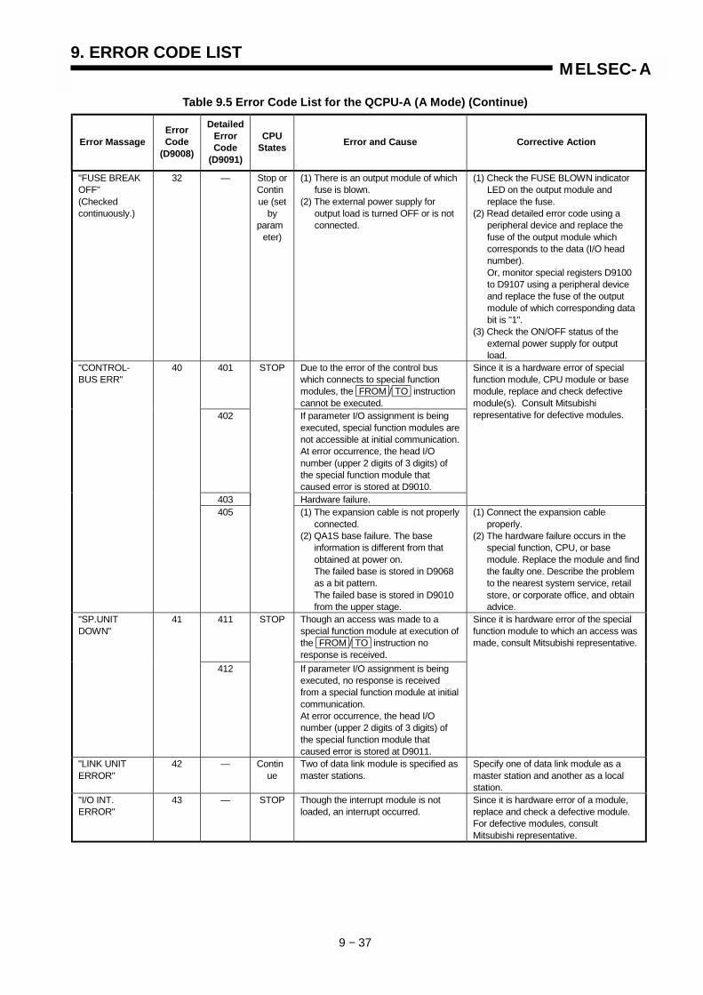
9. ERROR CODE LIST
9 − 37
MELSEC-A
Table 9.5 Error Code List for the QCPU-A (A Mode) (Continue)
Error MassageErrorCode
(D9008)
DetailedErrorCode
(D9091)
CPUStates Error and Cause Corrective Action
"FUSE BREAKOFF"(Checkedcontinuously.)
32 — Stop orContinue (set
byparam
eter)
(1) There is an output module of whichfuse is blown.
(2) The external power supply foroutput load is turned OFF or is notconnected.
(1) Check the FUSE BLOWN indicatorLED on the output module andreplace the fuse.
(2) Read detailed error code using aperipheral device and replace thefuse of the output module whichcorresponds to the data (I/O headnumber).Or, monitor special registers D9100to D9107 using a peripheral deviceand replace the fuse of the outputmodule of which corresponding databit is "1".
(3) Check the ON/OFF status of theexternal power supply for outputload.
401 Due to the error of the control buswhich connects to special functionmodules, the FROM / TO instructioncannot be executed.
402 If parameter I/O assignment is beingexecuted, special function modules arenot accessible at initial communication.At error occurrence, the head I/Onumber (upper 2 digits of 3 digits) ofthe special function module thatcaused error is stored at D9010.
403 Hardware failure.
Since it is a hardware error of specialfunction module, CPU module or basemodule, replace and check defectivemodule(s). Consult Mitsubishirepresentative for defective modules.
"CONTROL-BUS ERR"
40
405
STOP
(1) The expansion cable is not properlyconnected.
(2) QA1S base failure. The baseinformation is different from thatobtained at power on.The failed base is stored in D9068as a bit pattern.The failed base is stored in D9010from the upper stage.
(1) Connect the expansion cableproperly.
(2) The hardware failure occurs in thespecial function, CPU, or basemodule. Replace the module and findthe faulty one. Describe the problemto the nearest system service, retailstore, or corporate office, and obtainadvice.
411 Though an access was made to aspecial function module at execution ofthe FROM / TO instruction noresponse is received.
"SP.UNITDOWN"
41
412
STOP
If parameter I/O assignment is beingexecuted, no response is receivedfrom a special function module at initialcommunication.At error occurrence, the head I/Onumber (upper 2 digits of 3 digits) ofthe special function module thatcaused error is stored at D9011.
Since it is hardware error of the specialfunction module to which an access wasmade, consult Mitsubishi representative.
"LINK UNITERROR"
42 — Continue
Two of data link module is specified asmaster stations.
Specify one of data link module as amaster station and another as a localstation.
"I/O INT.ERROR"
43 — STOP Though the interrupt module is notloaded, an interrupt occurred.
Since it is hardware error of a module,replace and check a defective module.For defective modules, consultMitsubishi representative.

9. ERROR CODE LIST
9 − 38
MELSEC-A
Table 9.5 Error Code List for the QCPU-A (A Mode) (Continue)
Error MassageErrorCode
(D9008)
DetailedErrorCode
(D9091)
CPUStates Error and Cause Corrective Action
441 A special function module is assignedas an I/O module, or vice versa, in theI/O assignment using parameters fromthe peripheral device.
Execute I/O assignment again usingparameters from the peripheral deviceaccording to the loading status of specialfunction modules.
442 There are 9 or more special functionmodules (except the interrupt module)which can execute interruption to theCPU module loaded.
Reduce the special function modules(except the interrupt module) which canexecute interrupt start to 8 or less.
443 There are 2 or more data link modulesloaded.
Reduce the data link modules to 1 orless.
444 There are 7 or more modules such asa computer link module loaded to oneCPU module.
Reduce the computer link modules to 6or less.
445 There are 2 or more interrupt modulesloaded.
Reduce the interrupt modules to 1.
446 Modules assigned by parameters forMNT/MINI automatic refresh from theperipheral device do not conform withthe types of station modules actuallylinked.
Perform again module assignment forMNT/MINI automatic refresh withparameters according to actually linkedstation modules.
The number of modules of I/Oassignment registration (number ofloaded modules) per one CPUmodule for the special functionmodules which can use dedicatedinstructions is larger than thespecified limit. (Total of the numberof computers shown below is largerthan 1344.)
(A1SJ71C24-R2(PRF/R4) × 10)(A1SJ71UC24 × 10)
(A1SJ71PT32-S3 × 125)+ (A1SJ71PT32(S3) * × 125)
Reduce the number of loaded specialfunction modules.*Available when the extension mode isused.
447
Total > 1344448 (1) Five or more network modules
have been installed.(2) A total of five or more of network
modules and data link moduleshave been installed.
(1) Reduce the number to four or less.(2) Reduce the total number to four or
less.
"SP.UNITLAY.ERR."
44
449
STOP
An invalid base module is used.Failure of base module hardware.
Use an available base module.Replace the failed base module.
461 Module specified by the FROM / TOinstruction is not a special functionmodule.
Read the error step using a peripheraldevice and check and correct contentsof the FROM / TO instruction of thestep.
"SP.UNITERROR"(Checked atexecution of theFROM/TOinstruction or thededicatedinstructions forspecial functionmodules.)
46
462
Stop orContinue (set
byparam
eter)(1) Module specified by the dedicated
instruction for special functionmodule is not a special functionmodule or not a correspondingspecial function module.
(2) A command was issued to a CC-Link module with function versionunder B.
(3) A CC-Link dedicated commandwas issued to a CC-Link module forwhich the network parameters havenot been set.
(1) Read the error step using aperipheral device and check andcorrect contents of the dedicatedinstruction for special functionmodules of the step.
(2) Replace with a CC-Link modulehaving function version B and above.
(3) Set the parameters.

9. ERROR CODE LIST
9 − 39
MELSEC-A
Table 9.5 Error Code List for the QCPU-A (A Mode) (Continue)
Error MassageErrorCode
(D9008)
DetailedErrorCode
(D9091)
CPUStates Error and Cause Corrective Action
0 [When using MELSECNET/(II)](1) When the link range at a data link
CPU which is also a master station(station number = 00) is set byparameter setting at a peripheraldevice, for some reason the datawritten to the link parameter areadiffers from the link parameter dataread by the CPU. Alternatively, nolink parameters have been written.
(2) The total number of slave stationsis set at 0.
(1) Write the parameters again andcheck.
(2) Check the station number settings.(3) Persistent error occurrence may
indicate a hardware fault. Consultyour nearest Mitsubishirepresentative, explaining the natureof the problem.
470 [When using MELSECNET/10](1) The contents of the network refresh
parameters written from aperipheral device differ from theactual system at the base unit.
(2) The network refresh parametershave not been written.
471 [When using MELSECNET/10](1) The transfer source device range
and transfer destination devicerange specified for the inter-network transfer parameters are inthe same network.
(2) The specified range of transfersource devices or transferdestination devices for the inter-network transfer parameters spanstwo or more networks.
(3) The specified range of transfersource devices or transferdestination devices for the inter-network transfer parameters is notused by the network.
472 [When using MELSECNET/10]The contents of the routing parameterswritten from a peripheral device differfrom the actual network system.
Write the network refresh parametersagain and check.
473 [When using MELSECNET/10](1) The contents of the network
parameters for the first link unit,written from a peripheral device,differ from the actual networksystem.
(2) The link parameters for the first linkunit have not been written.
(3) The setting for the total number ofstations is 0.
"LINK PARA.ERROR"
47
474
Stop orContinue (set
byparam
eter)
[When using MELSECNET/10](1) The contents of the network
parameters for the second link unit,written from a peripheral device,differ from the actual networksystem.
(2) The link parameters for the secondlink unit have not been written.
(3) The setting for the total number ofstations is 0.
(1) Write the parameters again andcheck.
(2) Check the station number settings.(3) Persistent error occurrence may
indicate a hardware fault. Consultyour nearest Mitsubishirepresentative, explaining the natureof the problem.

9. ERROR CODE LIST
9 − 40
MELSEC-A
Table 9.5 Error Code List for the QCPU-A (A Mode) (Continue)
Error MassageErrorCode
(D9008)
DetailedErrorCode
(D9091)
CPUStates Error and Cause Corrective Action
475 [When using MELSECNET/10](1) The contents of the network
parameters for the third link unit,written from a peripheral device,differ from the actual networksystem.
(2) The link parameters for the thirdlink unit have not been written.
(3) The setting for the total number ofstations is 0.
476 [When using MELSECNET/10](1) The contents of the network
parameters for the fourth link unit,written from a peripheral device,differ from the actual networksystem.
(2) The link parameters for the fourthlink unit have not been written.
(3) The setting for the total number ofstations is 0.
"LINK PARA.ERROR"
47
477
Stop orContinue (set
byparam
eter)
A link parameter error was detected bythe CC-Link module.
(1) Write the parameters again andcheck.
(2) Check the station number settings.(3) Persistent error occurrence may
indicate a hardware fault. Consultyour nearest Mitsubishirepresentative, explaining the natureof the problem.
501 (1) When file registers (R) are used,operation is executed outside ofspecified ranges of device numbersand block numbers of file registers(R).
(2) File registers are used in theprogram without setting capacity offile registers.
502 Combination of the devices specifiedby instruction is incorrect.
503 Stored data or constant of specifieddevice is not in the unable range.
504 Set number of data to be handled isout of the unable range.
505 (1) Station number specified by theLEDA/ B LRDP , LEDA/B LWTP, LRDP , LWTP instructions is nota local station.
(2) Head I/O number specified by theLEDA/ B RFRP , LEDA/ B RTOP, RFRP , RTOP instructions is notof a remote station.
"OPERATIONERROR"(Checked atexecution ofinstruction.)
50
506
Stop orContinue (set
byparam
eter)
Head I/O number specified by theLEDA/ B RFRP , LEDA/ B RTOP, RFRP , RTOP instructions is not of aspecial function module.
Read the error step using a peripheraldevice and check and correct programof the step.
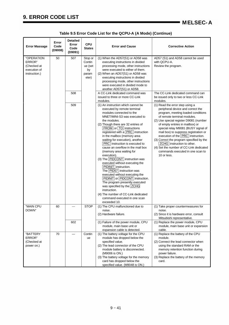
9. ERROR CODE LIST
9 − 41
MELSEC-A
Table 9.5 Error Code List for the QCPU-A (A Mode) (Continue)
Error MassageErrorCode
(D9008)
DetailedErrorCode
(D9091)
CPUStates Error and Cause Corrective Action
507 (1) When the AD57(S1) or AD58 wasexecuting instructions in dividedprocessing mode, other instructionswere executed to either of them.
(2) When an AD57(S1) or AD58 wasexecuting instructions in dividedprocessing mode, other instructionswere executed in divided mode toanother AD57(S1) or AD58.
AD57 (S1) and AD58 cannot be usedwith QCPU-A.Review the program.
508 A CC-Link dedicated command wasissued to three or more CC-Linkmodules.
The CC-Link dedicated command canbe issued only to two or less CC-Linkmodules.
"OPERATIONERROR"(Checked atexecution ofinstruction.)
50
509
Stop orContinue (set
byparam
eter)
(1) An instruction which cannot beexecuted by remote terminalmodules connected to theMNET/MINI-S3 was executed tothe modules.
(2) Though there are 32 entries of FROM or TO instructionsregistered with a PRC instructionin the mailbox (memory areawaiting for execution), another PRC instruction is executed tocause an overflow in the mail box(memory area waiting forexecution).
(3) The PIDCONT instruction wasexecuted without executing the PIDINIT instruction.The PID57 instruction wasexecuted without executing the PIDINIT or PIDCONT instruction.The program presently executedwas specified by the ZCHGinstruction.
(4) The number of CC-Link dedicatedcommand executed in one scanexceeded 10.
(1) Read the error step using aperipheral device and correct theprogram, meeting loaded conditionsof remote terminal modules.
(2) Use special register D9081 (numberof empty entries in mailbox) orspecial relay M9081 (BUSY signal ofmail box) to suppress registration orexecution of the PRC instruction.
(3) Correct the program specified by the ZCHG instruction to other.
(4) Set the number of CC-Link dedicatedcommands executed in one scan to10 or less.
— (1) The CPU malfunctioned due tonoise.
(2) Hardware failure.
(1) Take proper countermeasures fornoise.
(2) Since it is hardware error, consultMitsubishi representative.
"MAIN CPUDOWN"
60
602
STOP
(1) Failure of the power module, CPUmodule, main base unit orexpansion cable is detected.
(1) Replace the power module, CPUmodule, main base unit or expansioncable.
"BATTERYERROR"(Checked atpower on.)
70 — Continue
(1) The battery voltage for the CPUmodule has dropped below thespecified value.
(2) The lead connector of the CPUmodule battery is disconnected.(M9006 is ON.)
(3) The battery voltage for the memorycard has dropped below thespecified value. (M9048 is ON.)
(1) Replace the battery of the CPUmodule.
(2) Connect the lead connector whenusing the standard RAM or thememory retention function duringpower failure.
(3) Replace the battery of the memorycard.

MEMO

APP - 1
MELSEC-AAPPENDICES
APP
Appendix 1 LISTS OF SPECIAL RELAYS AND SPECIAL REGISTERS
Appendix 1.1 List of Special Relays
The special relays are the internal relays that have specific applications in thesequencer. Therefore, do not turn the special register ON/OFF on the program.(Except for the ones marked by 1 or 2 in the table.)
Table 1.1 Special Relay ListNumber Name Description Details Applicable CPU
1M9000 Fuse blown
OFF: NormalON: Fuse blown unit
• Turned on when there is one or more output units ofwhich fuse has been blown or external power supplyhas been turned off (only for small type). Remains onif normal status is restored.Output modules of remote I/O stations are alsochecked fore fuse condition.
Usable with alltypes of CPUs
Only remote I/Ostationinformation isvalid for A2C.
2M9002
I/O unitverify error
OFF: NormalON: Error
• Turned on if the status of I/O module is different fromentered status when power is turned on. Remains onif normal status is restored.I/O module verification is done also to remote I/Ostation modules.(Reset is enabled only when special registers D9116to D9123 are reset.)
Usable with alltypes of CPUs
Only remote I/Ostationinformation isvalid for A2C.
M9004 MINI link mastermodule error
OFF: NormalON: Error
• Turned on when the MINI (S3) link error is detectedon even one of the MINI (S3) link modules beingloaded. Remains on if normal status is restored.
—Dedicated to AnA,A2AS, AnU andQCPU-A (A Mode).
1M9005
AC DOWNdetection
OFF: AC power goodON: AC power DOWN
• Turned on when an momentary power failure of 20msec or less occurred.Reset when POWER switch is moved from OFF toON position.
Usable with alltypes of CPUs.
M9006 Battery low OFF: NormalON: Battery low
• Turned on when battery voltage reduces to less thanspecified. Turned off when battery voltage becomesnormal.
Usable with alltypes of CPUs.
1M9007
Battery low latch OFF: NormalON: Battery low
• Turned on when battery voltage reduces to less thanspecified. Remains on if battery voltage becomesnormal
Usable with alltypes of CPUs.
1M9008
Self-diagnosticerror
OFF: No errorON: Error
• Turned on when error is found as a result of self-diagnosis.
Usable with alltypes of CPUs.
M9009Annunciatordetection
OFF: No detectionON: Detected
• Turned on when OUT F of SET F instruction isexecuted. Switched off when D9124 data is zeroed.
Usable with alltypes of CPUs.
M9010 Operationerror flag
OFF: No errorON: Error
• Turned on when operation error occurs duringexecution of application instruction. Turned off whenerror is eliminated.
Unusable withA3H, A3M, AnA,A2AS, A3A board,AnU and QCPU-A(A Mode).
1M9011
Operationerror flag
OFF: No errorON: Error
• Turned on when operation error occurs duringexecution of application instruction. Remains on ifnormal status is restored.
Usable with alltypes of CPUs.
M9012 Carry flagOFF: Carry offON: Carry on
• Carry flag used in application instruction.Usable with alltypes of CPUs.
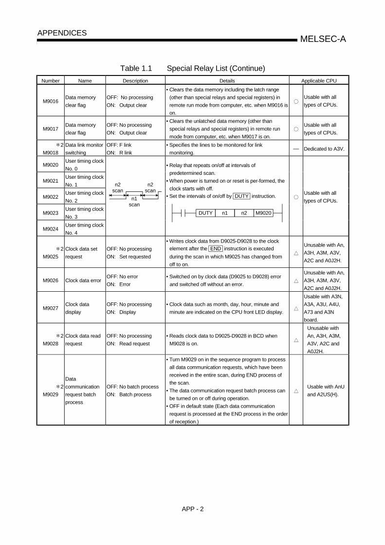
APP - 2
MELSEC-AAPPENDICES
Table 1.1 Special Relay List (Continue)Number Name Description Details Applicable CPU
M9016Data memoryclear flag
OFF: No processingON: Output clear
• Clears the data memory including the latch range(other than special relays and special registers) inremote run mode from computer, etc. when M9016 ison.
Usable with alltypes of CPUs.
M9017Data memoryclear flag
OFF: No processingON: Output clear
• Clears the unlatched data memory (other thanspecial relays and special registers) in remote runmode from computer, etc. when M9017 is on.
Usable with alltypes of CPUs.
2M9018
Data link monitorswitching
OFF: F linkON: R link
• Specifies the lines to be monitored for linkmonitoring.
— Dedicated to A3V.
M9020User timing clockNo. 0
M9021User timing clockNo. 1
M9022User timing clockNo. 2
M9023User timing clockNo. 3
M9024User timing clockNo. 4
n2scan
n1scan
n2scan
• Relay that repeats on/off at intervals ofpredetermined scan.
• When power is turned on or reset is per-formed, theclock starts with off.
• Set the intervals of on/off by DUTY instruction.
DUTY n1 n2 M9020
Usable with alltypes of CPUs.
2M9025
Clock data setrequest
OFF: No processingON: Set requested
• Writes clock data from D9025-D9028 to the clockelement after the END instruction is executedduring the scan in which M9025 has changed fromoff to on.
Unusable with An,A3H, A3M, A3V,A2C and A0J2H.
M9026 Clock data errorOFF: No errorON: Error
• Switched on by clock data (D9025 to D9028) errorand switched off without an error.
Unusable with An,A3H, A3M, A3V,A2C and A0J2H.
M9027Clock datadisplay
OFF: No processingON: Display
• Clock data such as month, day, hour, minute andminute are indicated on the CPU front LED display.
Usable with A3N,A3A, A3U, A4U,A73 and A3Nboard.
2M9028
Clock data readrequest
OFF: No processingON: Read request
• Reads clock data to D9025-D9028 in BCD whenM9028 is on.
Unusable withAn, A3H, A3M,A3V, A2C andA0J2H.
2M9029
Datacommunicationrequest batchprocess
OFF: No batch processON: Batch process
• Turn M9029 on in the sequence program to processall data communication requests, which have beenreceived in the entire scan, during END process ofthe scan.
• The data communication request batch process canbe turned on or off during operation.
• OFF in default state (Each data communicationrequest is processed at the END process in the orderof reception.)
Usable with AnUand A2US(H).

APP - 3
MELSEC-AAPPENDICES
Table 1.1 Special Relay List (Continue)Number Name Description Details Applicable CPU
M9030 0.1 second clock0.05
seconds 0.05seconds
M9031 0.2 second clock0.1
seconds 0.1seconds
M9032 1 second clock0.5
seconds 0.5seconds
M9033 2 second clock1
second 1second
M9034 1 minute clock30
seconds 30seconds
• 0.1 second, 0.2 second, 1 second, 2 second, and 1minute clocks are generated.
• Not turned on and off per scan but turned on and offeven during scan if corresponding time has elapsed.
• Starts with off when power is turned on or reset isperformed.
Unusable withA3V.
M9036 Normally ONONOFF
M9037 Normally OFFONOFF
M9038On only for 1scan after run
ONOFF 1 scan
M9039RUN flag(off only for 1scan after run)
ONOFF
1 scan
• Used as dummy contacts of initialization andapplication instruction in sequence program.
• M9036 and M9037 are turned on and off withoutregard to position of key switch on CPU front. M9038and M9039 are under the same condition as RUNstatus except when the key switch is at STOPposition, and turned off and on. Switched off if thekey switch is in STOP position. M9038 is on for onescan only and M9039 is off for one scan only if thekey switch is not in STOP position.
Usable with alltypes of CPU
M9040PAUSE enablecoil
OFF: PAUSE disabledON: PAUSE enabled
M9041PAUSE statuscontact
OFF: Not during pauseON: During pause
• When RUN key switch is at PAUSE position orremote pause contact has turned on and if M9040 ison, PAUSE mode is set and M9041 is turned on.
Usable with alltypes of CPU
M9042Stop statuscontact
OFF: Not during stopON: During stop
• Switched on when the RUN key switch is in STOPposition.
Usable with alltypes of CPU
M9043Sampling tracecompletion
OFF: During samplingtrace
ON: Sampling tracecompletion
• Turned on upon completion of sampling traceperformed the number of times preset by parameterafter STRA instruction is executed.Reset when STRAR instruction is executed.
Unusable with A1and A1N.
M9044 Sampling trace
OFF ON: STRA Same as executionON OFF: STRAR Same as execution
• Turning on/off M9044 can execute STRA / STRAR instruction.(M9044 is forcibly turned on/off by a peripheraldevice.)When switched from OFF to ON: STRA instructionWhen switched from ON to OFF: STRAR instructionThe value stored in D9044 is used as the conditionfor the sampling trace.At scanning, at time Time (10 msec unit)
Unusable with A1and A1N.
M9045Watchdog timer(WDT) reset
OFF: WDT not resetON: WDT reset
• Turn on M9045 to reset the WDT upon execution ofa ZCOM instruction or data communication requestbatch process. (Use this function for scan timesexceeding 200 ms.)
Unusable with A1and A1N.
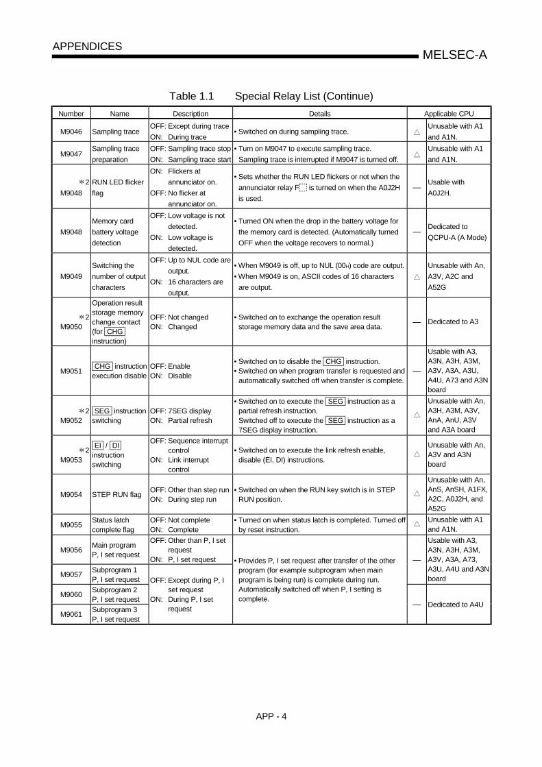
APP - 4
MELSEC-AAPPENDICES
Table 1.1 Special Relay List (Continue)Number Name Description Details Applicable CPU
M9046 Sampling traceOFF: Except during traceON: During trace
• Switched on during sampling trace.Unusable with A1and A1N.
M9047Sampling tracepreparation
OFF: Sampling trace stopON: Sampling trace start
• Turn on M9047 to execute sampling trace.Sampling trace is interrupted if M9047 is turned off.
Unusable with A1and A1N.
2M9048
RUN LED flickerflag
ON: Flickers atannunciator on.
OFF: No flicker atannunciator on.
• Sets whether the RUN LED flickers or not when theannunciator relay F is turned on when the A0J2His used.
— Usable withA0J2H.
M9048Memory cardbattery voltagedetection
OFF: Low voltage is notdetected.
ON: Low voltage isdetected.
• Turned ON when the drop in the battery voltage forthe memory card is detected. (Automatically turnedOFF when the voltage recovers to normal.)
— Dedicated toQCPU-A (A Mode)
M9049Switching thenumber of outputcharacters
OFF: Up to NUL code areoutput.
ON: 16 characters areoutput.
• When M9049 is off, up to NUL (00H) code are output.• When M9049 is on, ASCII codes of 16 characters
are output.
Unusable with An,A3V, A2C andA52G
2M9050
Operation resultstorage memorychange contact(for CHG instruction)
OFF: Not changedON: Changed
• Switched on to exchange the operation resultstorage memory data and the save area data. — Dedicated to A3
M9051 CHG instructionexecution disable
OFF: EnableON: Disable
• Switched on to disable the CHG instruction.• Switched on when program transfer is requested and
automatically switched off when transfer is complete.—
Usable with A3,A3N, A3H, A3M,A3V, A3A, A3U,A4U, A73 and A3Nboard
2M9052
SEG instructionswitching
OFF: 7SEG displayON: Partial refresh
• Switched on to execute the SEG instruction as apartial refresh instruction.Switched off to execute the SEG instruction as a7SEG display instruction.
Unusable with An,A3H, A3M, A3V,AnA, AnU, A3Vand A3A board
2M9053
EI / DI instructionswitching
OFF: Sequence interruptcontrol
ON: Link interruptcontrol
• Switched on to execute the link refresh enable,disable (EI, DI) instructions.
Unusable with An,A3V and A3Nboard
M9054 STEP RUN flag OFF: Other than step runON: During step run
• Switched on when the RUN key switch is in STEPRUN position.
Unusable with An,AnS, AnSH, A1FX,A2C, A0J2H, andA52G
M9055 Status latchcomplete flag
OFF: Not completeON: Complete
• Turned on when status latch is completed. Turned offby reset instruction.
Unusable with A1and A1N.
M9056 Main programP, I set request
OFF: Other than P, I setrequest
ON: P, I set request
M9057 Subprogram 1P, I set request
—
Usable with A3,A3N, A3H, A3M,A3V, A3A, A73,A3U, A4U and A3Nboard
M9060 Subprogram 2P, I set request
M9061 Subprogram 3P, I set request
OFF: Except during P, Iset request
ON: During P, I setrequest
• Provides P, I set request after transfer of the otherprogram (for example subprogram when mainprogram is being run) is complete during run.Automatically switched off when P, I setting iscomplete.
— Dedicated to A4U
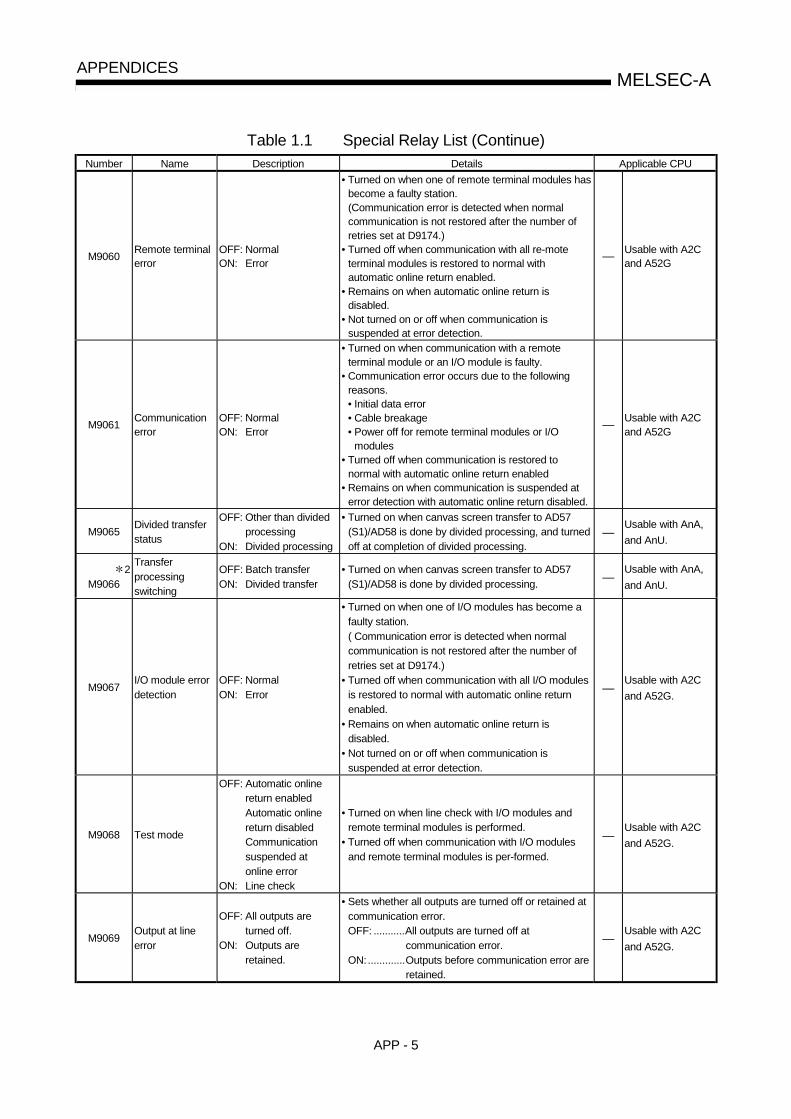
APP - 5
MELSEC-AAPPENDICES
Table 1.1 Special Relay List (Continue)Number Name Description Details Applicable CPU
M9060 Remote terminalerror
OFF: NormalON: Error
• Turned on when one of remote terminal modules hasbecome a faulty station.(Communication error is detected when normalcommunication is not restored after the number ofretries set at D9174.)
• Turned off when communication with all re-moteterminal modules is restored to normal withautomatic online return enabled.
• Remains on when automatic online return isdisabled.
• Not turned on or off when communication issuspended at error detection.
— Usable with A2Cand A52G
M9061 Communicationerror
OFF: NormalON: Error
• Turned on when communication with a remoteterminal module or an I/O module is faulty.
• Communication error occurs due to the followingreasons.• Initial data error• Cable breakage• Power off for remote terminal modules or I/O
modules• Turned off when communication is restored to
normal with automatic online return enabled• Remains on when communication is suspended at
error detection with automatic online return disabled.
— Usable with A2Cand A52G
M9065 Divided transferstatus
OFF: Other than dividedprocessing
ON: Divided processing
• Turned on when canvas screen transfer to AD57(S1)/AD58 is done by divided processing, and turnedoff at completion of divided processing.
—Usable with AnA,and AnU.
2M9066
Transferprocessingswitching
OFF: Batch transferON: Divided transfer
• Turned on when canvas screen transfer to AD57(S1)/AD58 is done by divided processing. —
Usable with AnA,and AnU.
M9067I/O module errordetection
OFF: NormalON: Error
• Turned on when one of I/O modules has become afaulty station.( Communication error is detected when normalcommunication is not restored after the number ofretries set at D9174.)
• Turned off when communication with all I/O modulesis restored to normal with automatic online returnenabled.
• Remains on when automatic online return isdisabled.
• Not turned on or off when communication issuspended at error detection.
—Usable with A2Cand A52G.
M9068 Test mode
OFF: Automatic onlinereturn enabledAutomatic onlinereturn disabledCommunicationsuspended atonline error
ON: Line check
• Turned on when line check with I/O modules andremote terminal modules is performed.
• Turned off when communication with I/O modulesand remote terminal modules is per-formed.
—Usable with A2Cand A52G.
M9069Output at lineerror
OFF: All outputs areturned off.
ON: Outputs areretained.
• Sets whether all outputs are turned off or retained atcommunication error.OFF: ...........All outputs are turned off at
communication error.ON:.............Outputs before communication error are
retained.
—Usable with A2Cand A52G.

APP - 6
MELSEC-AAPPENDICES
Table 1.1 Special Relay List (Continue)Number Name Description Details Applicable CPU
2M9070
Time required forsearch ofA8UPU/A8PUJ
OFF: Reading timereduction OFF
ON: Reading timereduction ON
• Turn on to reduce the search time of A8UPU/A8PUJ.(In this case, the scan time of the CPU moduleextends by 10%.)
Usable with AnUand A2US(H).
1M9073 WDT error flag
OFF: No WDT errorON: WDT error
• Turns on when WDT error is detected by the self-check of the PCPU. — Dedicated to A73.
M9073 Clock data setrequest
OFF: No processingON: Set request is made
• The clock data registered in D9073 to D9076 iswritten to the clock device after the execution of theEND instruction of the scan in which the state ofM9073 changes from OFF to ON.
—Dedicated toA2CCPUC24(-PRF)
M9073 Setting of writingto flash ROM
OFF: Disables writing toROM
ON: Enables writing toROM
• Turned on to enable writing to the flash ROM.(DIP switch 3 should be set to ON.) —
Dedicated toQCPU-A (A Mode)
M9074 PCPU readycomplete flag
OFF: PCPU readyincomplete
ON: PCPU readycomplete
• Set if the motor is not running when it is checked atPC ready (M2000) on. Turned off when M2000 isturned off.
— Dedicated to A73.
M9074 Clock data error OFF: No errorON: Error occurred
• This goes ON when a clock data (D9073 to D9076)error occurs. This remains OFF when there is noerror.
—Dedicated toA2CCPUC24(-PRF)
M9074Request forwriting to flashROM
OFF ON: Starts writingto ROM
• When turned from OFF to ON, writing to the standardROM is started. —
Dedicated toQCPU-A (A Mode)
M9075 Test mode flagOFF: Other than test
modeON: Test mode
• Turned ON when a test mode request is made froma peripheral device. Reset when test mode isfinished.
— Dedicated to A73.
M9075
Successfulcompletion ofwriting tostandard ROM
OFF: Failed writing toROM
ON: Successfullycompleted writing toROM
• Turned on when writing to the standard ROM issuccessfully completed.(This status is stored in D9075.)
—Dedicated toQCPU-A (A Mode)
M9076Externalemergency stopinput flag
OFF: External emergencystop input is on.
ON: External emergencystop input is off.
• Turned off when the external emergency stop inputconnected to the EMG terminal of A70SF is turnedon. Turned on when the external emergency stopinput is turned off.
— Dedicated to A73.
M9076 Clock data readrequest
OFF: No procesingON: Read request is
made
• When M9076 is ON, clock data is read out to D9073to D9076 in BCD values. —
Dedicated toA2CCPUC24(-PRF)
M9076 Status of writingto standard ROM
OFF: Writing to ROMdisabled
ON: Writing to ROMenabled
• Turns ON when writing to standard ROM is enabled.(Turns ON when DIP switch and M9073 are ON.) —
Dedicated toQCPU-A (A Mode)
M9077Manual pulsegenerator axissetting error flag
OFF: All axes normalON: Error axis detected
• Turned on when there is an error in the contents ofmanual pulse generator axis setting. Turned off if allaxes are normal when the manual pulse generatorenable flag is turned on.
— Dedicated to A73.
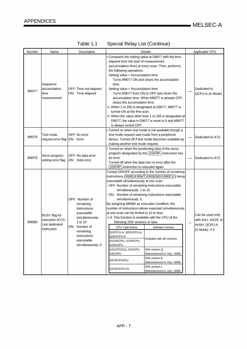
APP - 7
MELSEC-AAPPENDICES
Table 1.1 Special Relay List (Continue)Number Name Description Details Applicable CPU
M9077
Sequenceaccumulationtimemeasurement
OFF: Time not elapsedON: Time elapsed
• Compares the setting value at D9077 with the timeelapsed from the start of measurement(accumulation time) at every scan. Then, performsthe following operations:Setting value > Accumulation time:
Turns M9077 ON and clears the accumulationtime.
Setting value < Accumulation time:Turns M9077 from ON to OFF and clears theaccumulation time. When M9077 is already OFF,clears the accumulation time.
When 1 to 255 is designated at D9077, M9077 isturned ON at the first scan.
When the value other than 1 to 255 is designated atD9077, the value in D9077 is reset to 0 and M9077is always turned OFF.
—Dedicated toQCPU-A (A Mode)
M9078 Test moderequest error flag
OFF: No errorON: Error
• Turned on when test mode is not available though atest mode request was made from a peripheraldevice. Turned off if test mode becomes available bymaking another test mode request.
— Dedicated to A73.
M9079 Servo programsetting error flag
OFF: No data errorON: Data error
• Turned on when the positioning data of the servoprogram designated by the DSFRP instruction hasan error.Turned off when the data has no error after the DSFRP instruction is executed again.
— Dedicated to A73.
Turned ON/OFF according to the number of remaininginstructions ( RIRD / RIWT / RISEND / RIRCV ) beingexecutable simultaneously at one scan.
OFF: Number of remaining instructions executablesimultaneously: 1 to 10
ON: Number of remaining instructions executablesimultaneously: 0
By assigning M9080 as execution condition, thenumber of instructions above executed simultaneouslyat one scan can be limited to 10 or less.
4: This function is available with the CPU of thefollowing S/W versions or later.
CPU Type Name Software Version
Q02CPU-A, Q02HCPU-A,Q06HCPU-AA1SJHCPU, A1SHCPU,A2SHCPU
Available with all versions
A2UCPU(S1), A3UCPU,A4UCPU
S/W version Q(Manufactured in July, 1999)
A2USCPU(S1)S/W version E(Manufactured in July, 1999)
A2USHCPU-S1S/W version L(Manufactured in July, 1999)
M9080
BUSY flag forexecution of CC-Link dedicatedinstruction
OFF: Number ofremaininginstructionsexecutablesimultaneously:1 to 10
ON: Number ofremaininginstructionsexecutablesimultaneously: 0
Can be used onlywith AnU, A2US, orAnSH, QCPU-A(A Mode) 4

APP - 8
MELSEC-AAPPENDICES
Table 1.1 Special Relay List (Continue)Number Name Description Details Applicable CPU
M9081
Registration areabusy signal forcommunicationrequest
OFF: Communicationrequest to remoteterminal modulesenabled
ON: Communicationrequest to remoteterminal modulesdisabled
• Indication of communication enable/disable toremote terminal modules connected to the MINI (S3)link module, A2C or A52G.
—
Usable with AnA,AnA, AnU, A2AS,QCPU-A (A Mode)A2C and A52G.
M9082Final stationnumberdisagreement
OFF: Final stationnumber agreement
ON: Final stationnumberdisagreement
• Turned on when the final station number of theremote terminal modules and remote I/O modulesconnected to the A2C or A52G disagrees with thetotal number of stations set in the initial setting.
• Turned off when the final station number agrees withthe total number of stations at STOP RUN
—Dedicated to A2Cand A52G.
2M9084 Error check
OFF: Checks enabledON: Checks disabled
• Specify whether the following errors are to bechecked or not after the END instruction isexecuted (to set END instruction processing time):• Fuse blown• I/O unit verify error• Battery error
Unusable with An,A2C and A3V.
M9086BASIC programRUN flag
OFF: A3M-BASIC stopON: A3M-BASIC run
• Turned on when the A3M-BASIC is in RUN state,and turned off when it is in STOP state. — Dedicated to A3M
M9087 BASIC programPAUSE flag
OFF: A3M-BASIC RUNenable
ON: A3M-BASIC disable
• Specifies enable/disable of A3M-BASIC executionwhen the A3MCPU is in PAUSE state.OFF: A3M-BASIC is executed.ON: A3M-BASIC is not executed.
— Dedicated to A3M.
M9090Power supplyproblem statuson the PC side
OFF: NormalON: Power off
• Turns on if the power to the PC side is shut off whenthe external power supply is connected to the CPUboard.It stays on even after the status becomes normal.
— Dedicated toA2USH board
1M9091
Operation errordetail flag
OFF: No errorON: Error
• Turned on when an operation error detail factor isstored at D9091, and remains ON after normal stateis restored.
—Usable with AnA,A2AS, AnU andQCPU-A (A Mode).
M9091
Microcomputersubroutine callerror flag
OFF: No errorON: Error
• Turned on when an error occurred at execution ofthe microcomputer program package, and remainsON after normal state is restored.
—
Unusable withAnA, A2AS, AnUand QCPU-A(A Mode).
M9092External powersupply problemstatus
OFF: NormalON: Power off
• Turns on when the external power being supplied tothe CPU board is shut off.It stays on even after the status becomes normal.
— Dedicated toA2USH board
M9092Duplex powersupply overheaterror
OFF: NormalON: Overheat
• Turned on when overheat of a duplex power supplymodule is detected. — Dedicated to A3V.
M9093 Duplex powersupply error
OFF: NormalON: Failure or AC power
supply down
• Turned on when a duplex power supply modulecaused failure or the AC power supply is cut down. — Dedicated to A3V.
2 3M9094 I/O change flag OFF: Changed
ON: Not changed
• After the head address of the required I/O module isset to D9094, switching M9094 on allows the I/Omodule to be changed in online mode. (One moduleis only allowed to be changed by one setting.)
• To be switched on in the program or peripheraldevice test mode to change the module during CPURUN. To be switched on in peripheral device testmode to change the module during CPU STOP.
• RUN/STOP mode must not be changed until I/Omodule change is complete.
— Usable with An,AnN, AnA, AnU.
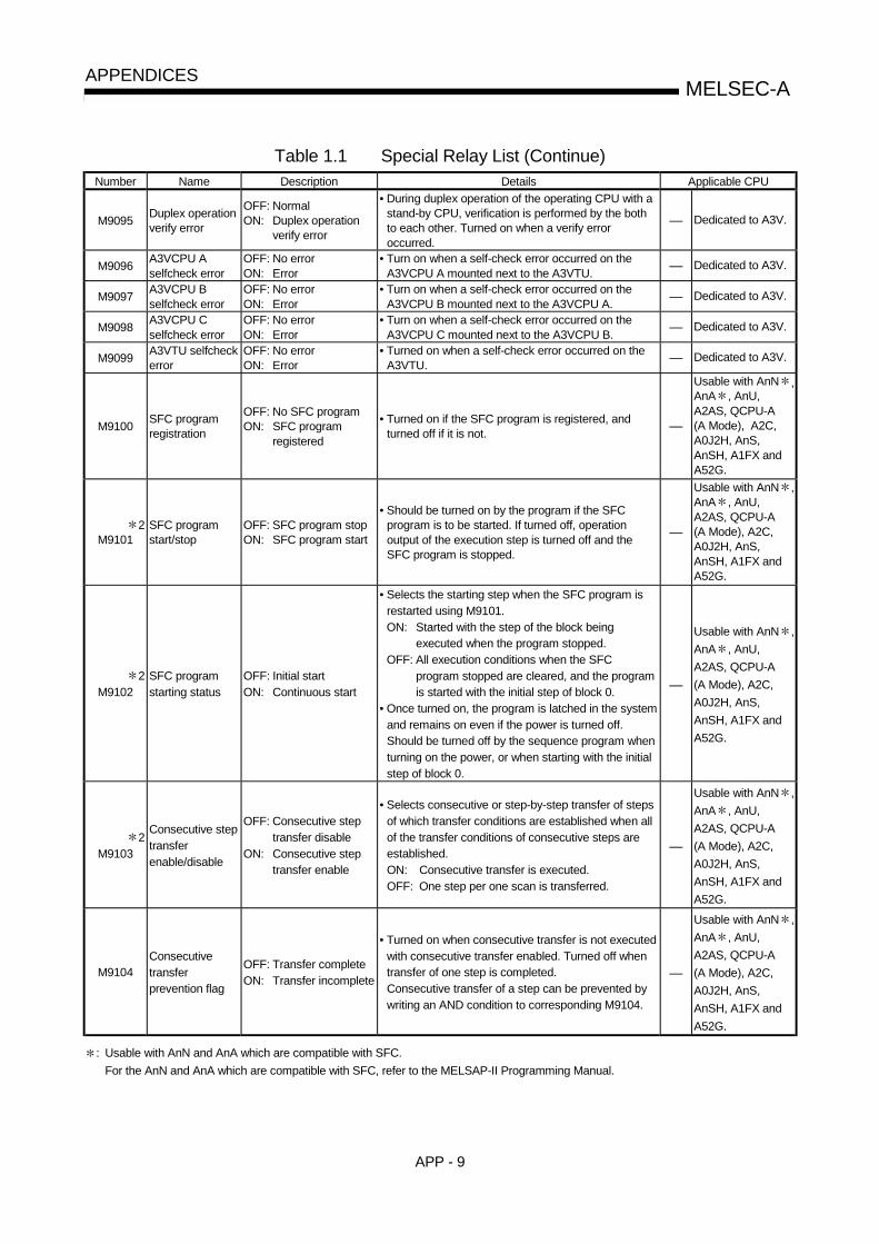
APP - 9
MELSEC-AAPPENDICES
Table 1.1 Special Relay List (Continue)Number Name Description Details Applicable CPU
M9095 Duplex operationverify error
OFF: NormalON: Duplex operation
verify error
• During duplex operation of the operating CPU with astand-by CPU, verification is performed by the bothto each other. Turned on when a verify erroroccurred.
— Dedicated to A3V.
M9096 A3VCPU Aselfcheck error
OFF: No errorON: Error
• Turn on when a self-check error occurred on theA3VCPU A mounted next to the A3VTU. — Dedicated to A3V.
M9097 A3VCPU Bselfcheck error
OFF: No errorON: Error
• Turn on when a self-check error occurred on theA3VCPU B mounted next to the A3VCPU A. — Dedicated to A3V.
M9098 A3VCPU Cselfcheck error
OFF: No errorON: Error
• Turn on when a self-check error occurred on theA3VCPU C mounted next to the A3VCPU B. — Dedicated to A3V.
M9099 A3VTU selfcheckerror
OFF: No errorON: Error
• Turned on when a self-check error occurred on theA3VTU. — Dedicated to A3V.
M9100 SFC programregistration
OFF: No SFC programON: SFC program
registered
• Turned on if the SFC program is registered, andturned off if it is not. —
Usable with AnN ,AnA , AnU,A2AS, QCPU-A(A Mode), A2C,A0J2H, AnS,AnSH, A1FX andA52G.
2M9101
SFC programstart/stop
OFF: SFC program stopON: SFC program start
• Should be turned on by the program if the SFCprogram is to be started. If turned off, operationoutput of the execution step is turned off and theSFC program is stopped.
—
Usable with AnN ,AnA , AnU,A2AS, QCPU-A(A Mode), A2C,A0J2H, AnS,AnSH, A1FX andA52G.
2M9102
SFC programstarting status
OFF: Initial startON: Continuous start
• Selects the starting step when the SFC program isrestarted using M9101.ON: Started with the step of the block being
executed when the program stopped.OFF: All execution conditions when the SFC
program stopped are cleared, and the programis started with the initial step of block 0.
• Once turned on, the program is latched in the systemand remains on even if the power is turned off.Should be turned off by the sequence program whenturning on the power, or when starting with the initialstep of block 0.
—
Usable with AnN ,AnA , AnU,A2AS, QCPU-A(A Mode), A2C,A0J2H, AnS,AnSH, A1FX andA52G.
2M9103
Consecutive steptransferenable/disable
OFF: Consecutive steptransfer disable
ON: Consecutive steptransfer enable
• Selects consecutive or step-by-step transfer of stepsof which transfer conditions are established when allof the transfer conditions of consecutive steps areestablished.ON: Consecutive transfer is executed.OFF: One step per one scan is transferred.
—
Usable with AnN ,AnA , AnU,A2AS, QCPU-A(A Mode), A2C,A0J2H, AnS,AnSH, A1FX andA52G.
M9104Consecutivetransferprevention flag
OFF: Transfer completeON: Transfer incomplete
• Turned on when consecutive transfer is not executedwith consecutive transfer enabled. Turned off whentransfer of one step is completed.Consecutive transfer of a step can be prevented bywriting an AND condition to corresponding M9104.
—
Usable with AnN ,AnA , AnU,A2AS, QCPU-A(A Mode), A2C,A0J2H, AnS,AnSH, A1FX andA52G.
: Usable with AnN and AnA which are compatible with SFC.For the AnN and AnA which are compatible with SFC, refer to the MELSAP-II Programming Manual.
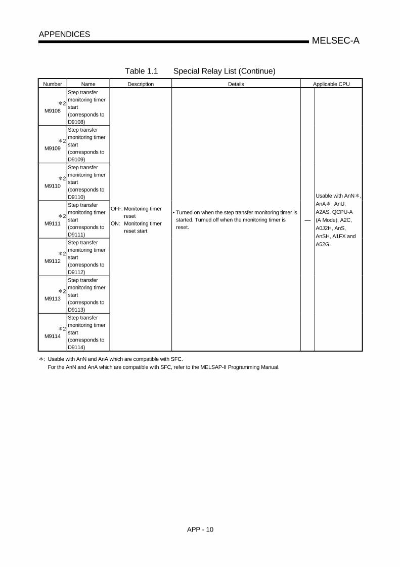
APP - 10
MELSEC-AAPPENDICES
Table 1.1 Special Relay List (Continue)Number Name Description Details Applicable CPU
2M9108
Step transfermonitoring timerstart(corresponds toD9108)
2M9109
Step transfermonitoring timerstart(corresponds toD9109)
2M9110
Step transfermonitoring timerstart(corresponds toD9110)
2M9111
Step transfermonitoring timerstart(corresponds toD9111)
2M9112
Step transfermonitoring timerstart(corresponds toD9112)
2M9113
Step transfermonitoring timerstart(corresponds toD9113)
2M9114
Step transfermonitoring timerstart(corresponds toD9114)
OFF: Monitoring timerreset
ON: Monitoring timerreset start
• Turned on when the step transfer monitoring timer isstarted. Turned off when the monitoring timer isreset.
—
Usable with AnN ,AnA , AnU,A2AS, QCPU-A(A Mode), A2C,A0J2H, AnS,AnSH, A1FX andA52G.
: Usable with AnN and AnA which are compatible with SFC.For the AnN and AnA which are compatible with SFC, refer to the MELSAP-II Programming Manual.
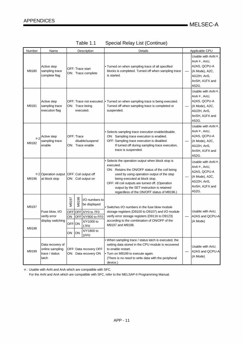
APP - 11
MELSEC-AAPPENDICES
Table 1.1 Special Relay List (Continue)Number Name Description Details Applicable CPU
M9180Active stepsampling tracecomplete flag
OFF: Trace startON: Trace complete
• Turned on when sampling trace of all specifiedblocks is completed. Turned off when sampling traceis started.
—
Usable with AnN ,AnA , AnU,A2AS, QCPU-A(A Mode), A2C,A0J2H, AnS,AnSH, A1FX andA52G.
M9181Active stepsampling traceexecution flag
OFF: Trace not executed.ON: Trace being
executed.
• Turned on when sampling trace is being executed.Turned off when sampling trace is completed orsuspended.
—
Usable with AnN ,AnA , AnU,A2AS, QCPU-A(A Mode), A2C,A0J2H, AnS,AnSH, A1FX andA52G.
2M9182
Active stepsampling traceenable
OFF: Tracedisable/suspend
ON: Trace enable
• Selects sampling trace execution enable/disable.ON: Sampling trace execution is enabled.OFF: Sampling trace execution is disabled.
If turned off during sampling trace execution,trace is suspended.
—
Usable with AnN ,AnA , AnU,A2AS, QCPU-A(A Mode), A2C,A0J2H, AnS,AnSH, A1FX andA52G.
2M9196
Operation outputat block stop
OFF: Coil output offON: Coil output on
• Selects the operation output when block stop isexecuted.ON: Retains the ON/OFF status of the coil being
used by using operation output of the stepbeing executed at block stop.
OFF: All coil outputs are turned off. (Operationoutput by the SET instruction is retainedregardless of the ON/OFF status of M9196.)
—
Usable with AnN ,AnA , AnU,A2AS, QCPU-A(A Mode), A2C,A0J2H, AnS,AnSH, A1FX andA52G.
M91
97
M91
98 I/O numbers tobe displayed
OFF OFF X/Y0 to 7F0M9197
ON OFF X/Y800 to FF0
OFF ONX/Y1000 to17F0
M9198
Fuse blow, I/Overify errordisplay switching
ON ONX/Y1800 to1FF0
• Switches I/O numbers in the fuse blow modulestorage registers (D9100 to D9107) and I/O moduleverify error storage registers (D9116 to D9123)according to the combination of ON/OFF of theM9197 and M9198.
—Usable with AnU,A2AS and QCPU-A(A Mode)
M9199
Data recovery ofonline samplingtrace / statuslatch
OFF: Data recovery OFFON: Data recovery ON
• When sampling trace / status latch is executed, thesetting data stored in the CPU module is recoveredto enable restart.
• Turn on M9199 to execute again.(There is no need to write data with the peripheraldevice.)
—Usable with AnU,A2AS and QCPU-A(A Mode)
: Usable with AnN and AnA which are compatible with SFC.For the AnN and AnA which are compatible with SFC, refer to the MELSAP-II Programming Manual.
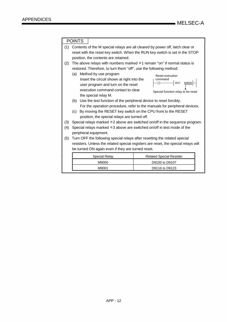
APP - 12
MELSEC-AAPPENDICES
POINTS(1) Contents of the M special relays are all cleared by power off, latch clear or
reset with the reset key switch. When the RUN key switch is set in the STOPposition, the contents are retained.
(2) The above relays with numbers marked 1 remain "on" if normal status isrestored. Therefore, to turn them "off", use the following method:(a) Method by use program
Insert the circuit shown at right into theuser program and turn on the resetexecution command contact to clearthe special relay M.
Reset executioncommand
RST M9000
Special function relay to be reset
(b) Use the test function of the peripheral device to reset forcibly.For the operation procedure, refer to the manuals for peripheral devices.
(c) By moving the RESET key switch on the CPU front to the RESETposition, the special relays are turned off.
(3) Special relays marked 2 above are switched on/off in the sequence program.(4) Special relays marked 3 above are switched on/off in test mode of the
peripheral equipment.(5) Turn OFF the following special relays after resetting the related special
resisters. Unless the related special registers are reset, the special relays willbe turned ON again even if they are turned reset.
Special Relay Related Special Resister
M9000 D9100 to D9107M9001 D9116 to D9123

APP - 13
MELSEC-AAPPENDICES
Appendix 1.2 Special Relays for Link
The link special relays are internal relays which are switched on/off by various factorsoccurring during data link operation.Their ON/OFF status will change if an error occurs during normal operation.These special registers are applicable to all types of CPUs except the A3V.For description of the special registers for link for the A3V, refer to the A3VTS DataLink System User’s Manual.
(1) Link special relays only valid when the host is the master station
Table 1.2 Link Special Relay ListNumber Name Description Details
M9200 LRDP instructionreceived
OFF: UnreceivedON: Received
• Depends on whether or not the LRDP (word device read)instruction has been received.
• Used in the program as an interlock for the LRDP instruction.
• Use the RST instruction to reset.
M9201 LRDP instructioncomplete
OFF: IncompleteON: Complete
• Depends on whether or not the LRDP (word device read)instruction execution is complete.
• Used as a condition contact for resetting M9200 and M9201after the LRDP instruction is complete.
• Use the RST instruction to reset.
M9202 LWTP instructionreceived
OFF: UnreceivedON: Received
• Depends on whether or not the LWTP (word device write)instruction has been received.
• Used in the program as an interlock for the LWTP nstruction.
• Use the RST instruction to reset.
M9203 LWTP instructioncomplete
OFF: IncompleteON: Complete
• Depends on whether or not the LWTP (word device write)instruction execution is complete.
• Used as a condition contact to reset M9202 and M9203 afterthe LWTP instruction is complete.
• Use the RST instruction to reset.
M9206Link parameter error inthe host
OFF: NormalON: Error
Depends on whether or not the link parameter setting of thehost is valid.
M9207Link parameterunmatched betweenmaster station
OFF: NormalON: Unmatched
Depends on whether or not the link parameter setting of themaster station in tier two matches that of the master station intier three in a three-tier system.(Valid only for the master stations in a three-tier system.)
M9210Link card error(master station)
OFF: NormalON: Error
Depends on presence or absence of the link card hardwareerror. Judged by the CPU.
M9224 Link statusOFF: OnlineON: Offline, station-to-station
test, or self-loopback test
Depends on whether the master station is online or offline or isin station-to-station test or self-loopback test mode.
M9225 Forward loop errorOFF: NormalON: Error
Depends on the error condition of the forward loop line.
M9226 Reverse loop errorOFF: NormalON: Error
Depends on the error condition of the reverse loop line.
M9227 Loop test statusOFF: UnexecutedON: Forward or reverse loop test
being executed
Depends on whether or not the master station is executing aforward or a reverse loop test.
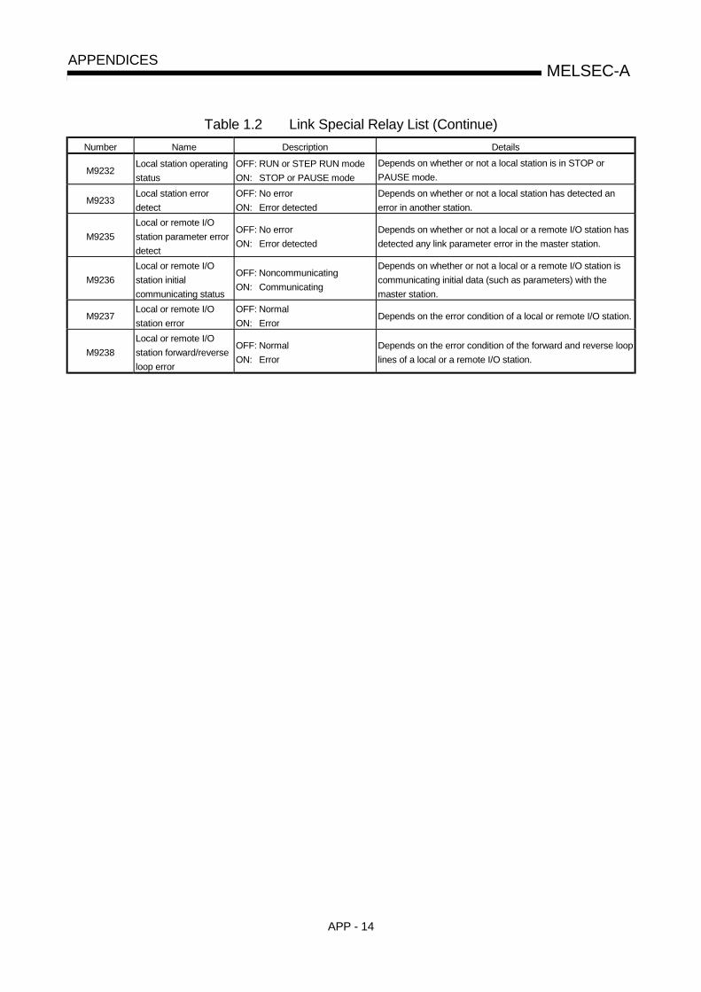
APP - 14
MELSEC-AAPPENDICES
Table 1.2 Link Special Relay List (Continue)Number Name Description Details
M9232Local station operatingstatus
OFF: RUN or STEP RUN modeON: STOP or PAUSE mode
Depends on whether or not a local station is in STOP orPAUSE mode.
M9233Local station errordetect
OFF: No errorON: Error detected
Depends on whether or not a local station has detected anerror in another station.
M9235Local or remote I/Ostation parameter errordetect
OFF: No errorON: Error detected
Depends on whether or not a local or a remote I/O station hasdetected any link parameter error in the master station.
M9236Local or remote I/Ostation initialcommunicating status
OFF: NoncommunicatingON: Communicating
Depends on whether or not a local or a remote I/O station iscommunicating initial data (such as parameters) with themaster station.
M9237Local or remote I/Ostation error
OFF: NormalON: Error
Depends on the error condition of a local or remote I/O station.
M9238Local or remote I/Ostation forward/reverseloop error
OFF: NormalON: Error
Depends on the error condition of the forward and reverse looplines of a local or a remote I/O station.

APP - 15
MELSEC-AAPPENDICES
(2) Link special relays only valid when the host is a local station
Table 1.3 Link Special Relay ListNumber Name Description Details
M9204 LRDP instructioncomplete
OFF: IncompleteON: Complete
On indicates that the LRDP instruction is complete at thelocal station.
M9205 LWTP instructioncomplete
OFF: IncompleteON: Complete
On indicates that the LWTP instruction is complete at thelocal station.
M9211Link card error(local station)
OFF: NormalON: Error
Depends on presence or absence of the link card error.Judged by the CPU.
M9240 Link statusOFF: OnlineON: Offline, station-to-station
test, or self-loopback test
Depends on whether the local station is online or offline, or isin station-to-station test or self-loopback test mode.
M9241 Forward loop errorOFF: NormalON: Error
Depends on the error condition of the forward loop line.
M9242 Reverse loop errorOFF: NormalON: Error
Depends on the error condition of the reverse loop line.
M9243 Loopback executionOFF: Non-executedON: Executed
Depends on whether or not loopback is occurring at the localstation.
M9246 Data unreceivedOFF: ReceivedON: Unreceived
Depends on whether or not data has been received from themaster station.
M9247 Data unreceivedOFF: ReceivedON: Unreceived
Depends on whether or not a tier three station has receiveddata from its master station in a three-tier system.
M9250 Parameter unreceivedOFF: ReceivedON: Unreceived
Depends on whether or not link parameters have beenreceived from the master station.
M9251 Link breakOFF: NormalON: Break
Depands on the data link condition at the local station.
M9252 Loop test statusOFF: UnexecutedON: Forward or reverse loop test
is being executed
Depends on whether or not the local station is executing aforward or a reverse loop test.
M9253Master stationoperating status
OFF: RUN or STEP RUN modeON: STOP or PAUSE mode
Depends on whether or not the master station is in STOP orPAUSE mode.
M9254Operating status ofother local stations
OFF: RUN or STEP RUN modeON: STOP or PAUSE mode
Depends on whether or not a local station other than the hostis in STOP or PAUSE mode.
M9255Error status of otherlocal stations
OFF: NormalON: Error
Depends on whether or not a local station other than the hostis in error.

APP - 16
MELSEC-AAPPENDICES
Appendix 1.3 Special Registers
Special registers are data registers of which applications have been determined insidethe PC. Therefore, do not write data to the special registers in the program (except theones with numbers marked 2 in the table).
Table 1.4 Special Register ListNumber Name Description Details Applicable CPU
D9000 Fuse blowFuse blow modulenumber
• When fuse blown modules are detected, the lowestnumber of detected units is stored in hexadecimal.(Example: When fuses of Y50 to 6F output modules haveblown, "50" is stored in hexadecimal) To monitor thenumber by peripheral devices, perform monitor operationgiven in hexadecimal.(Cleared when all contents of D9100 to D9107 are resetto 0.)
• Fuse blow check is executed also to the output modulesof remote I/O stations.
Unusable withA0J2H.
Only remoteI/O station in-formation isvalid for A2C.
• Stores the module numbers corresponding to settingswitch numbers or base slot numbers when fuse blowoccurred.
I/O Module for A0J2 Extension Base UnitSettingSwitch
Stored DataBase Unit
Slot No.Stored Data
0 1 0 51 2 1 62 3 2 73 4 3 84 55 66 77 8
D9001 Fuse blowFuse blow modulenumber
• In case of remote I/O station, (module I/O number/10H) +1 is stored.
—Dedicated toA0J2H.
• If I/O modules, of which data are different from dataentered, are detected when the power is turned on, thefirst I/O number of the lowest number unit among thedetected units is stored in hexadecimal. (Storing methodis the same as that of D9000.) To monitor the number byperipheral devices, perform monitor operation given inhexadecimal.(Cleared when all contents of D9116 to D9123 are resetto 0.)
• I/O module verify check is executed also to the modulesof remote I/O terminals.
Unusable withA0J2H.
Only remoteI/O station in-formation isvalid for A2C.
D9002 I/O module verifyerror
I/O module verify errorunit number
• If an I/O module, of which data is different from dataentered, is detected when the power in turned on, the I/Onumber corresponding to the setting switch No. or baseunit No. is stored.(Storing method is the same as that of D9001).
• In case of remote I/O station, (module I/O number/10H) +1 is stored.
—Dedicated toA0J2H.

APP - 17
MELSEC-AAPPENDICES
Table 1.4 Special Register List (Continue)Number Name Description Details Applicable CPU
D9003 SUM instructiondetection bits
The number of bitsdetected by SUMinstruction detection.
• The number of bits detected by execution of the SUMinstruction are stored. in BIN code and updated everyexecution thereafter.
—Dedicated toA0J2H.
1D9004
MINI link mastermodule error
Error detection status
• Error status of the MINI (S3) link detected on loadedMINI (S3) link module is stored.b15 b8 b7 b0
Bits which correspondto the signals of MINI (S3) link module, shown below, are turned on as the signals are turned on.Hardware error(X0/X20)MINI(S3) link errordetection (X6/X26) MINI(S3) link communication error(X7/X27)
to to
8 7 6 5 4 3 2 1 8 7 6 5 4 3 2 1
Data communication between the PLC CPU and MINI (S3) link module is disabled. —
Usable with AnA,A2AS, AnAboard and AnU.
1D9005
AC DOWNcounter
AC DOWN count• 1 is added each time input voltage becomes 85% or less
of rating while the CPU unit is performing operation, andthe value is stored in BIN code.
Usable with alltypes of CPUs.
D9006 Battery lowIndicates the CPUmodule of whichbattery voltage is low.
• Bits which correspond to CPU of which battery is low areturned on in D9006, as shown below.
0 0B3 B0B1B2
CPU BCPU C
CPU A0: Normal1: Battery low
B15
—Dedicated toA3V.
1D9008
Shelf-diagnosticerror
Self-diagnostic errornumber
• When error is found as a result of self-diagnosis, errornumber is stored in BIN code.
Usable with alltypes of CPUs.
• When one of F0 to 255 is turned on by OUT F or SET F , the F number, which has been detectedearliest among the F numbers which have turned on, isstored in BIN code.
• D9009 can be cleared by RST F or LEDR instruction.If another F number has been detected, the clearing ofD9009 causes the next number to be stored in D9009.
Unusable withA3, A3N, A3A,A73 and A3Nboard.
D9009 Annunciatordetection
F number at whichexternal failure hasoccurred
• When one of F0 to 255 is turned on by OUT F or SET F , the F number, which has been detected earliestamong the F numbers which have turned on, is stored inBIN code.
• D9009 can be cleared by executing RST F or LEDR instruction or moving INDICATOR RESET switch onCPU front to ON position. If another F number has beendetected, the clearing of D9009 causes the nest numberto be stored in D9009.
—Usable with A3,A3N, A3A, A73and A3N board.

APP - 18
MELSEC-AAPPENDICES
Table 1.4 Special Register List (Continue)Number Name Description Details Applicable CPU
D9010 Error stepStep number at whichoperation error hasoccurred
• When operation error has occurred during execution ofapplication instruction, the step number, at which theerror has occurred, is stored in BIN code. Thereafter,each time operation error occurs, the contents of D9010are renewed.
Unusable withA3H and A3M.
1D9011
Error stepStep number at whichoperation error hasoccurred
• When operation error has occurred during execution ofapplication instruction, the step number, at which theerror has occurred, is stored in BIN code. Since storageinto D9011 is made when M9011 changes from off to on,the contents of D9010 cannot be renewed unless M9011is cleared by user program.
Usable with alltypes of CPUs.
D9014 I/O control mode I/O control modenumber
• The I/O control mode set is returned in any of thefollowing numbers:0. Both input and output in direct mode1. Input in refresh mode, output in direct mode3. Both input and output in refresh mode
Unusable withAn, A3H andA3M.
D9015CPU operatingstates
Operating states ofCPU
• The operation states of CPU as shown below are storedin D9015.
01
Except belowinstruction executionSTOP
Status in program
B15 B12 B11 B8 B7 B4 B3 B0..... ...... ....... .......
Remote RUN/STOP by parameter setting
012
RUNSTOP
PAUSE
012
RUNSTOP
PAUSE
Remote RUN/STOP by computer
012
STOP
STEP RUNPAUSE
RUN
CPU key switch: Remains the same in remote RUN/STOP mode.
3
When the CPU is in RUN mode and M9040 is off, theCPU remains in RUN mode if changed to PAUSEmode.
Usable with alltypes of CPUs.

APP - 19
MELSEC-AAPPENDICES
Table 1.4 Special Register List (Continue)Number Name Description Details Applicable CPU
ROM/RAMsetting
0: ROM1: RAM2: E2PROM
• Indicates the setting of memory select chip. One value of0 to 2 is stored in BIN code. —
Usable with A1and A1N.
0: Main program(ROM)
1: Main program (RAM)2: Subprogram (RAM)
• Indicates which sequence program is run presently. Onevalue of 0 to 2 is stored in BIN code.("2" is not stored when AnS, AnSH, A1FX, A0J2H, A2C,A2, A2N, A2A, A2AS and A2U is used.)
Unusable with A1and A1N
D9016
Program number
0: Main program(ROM)
1: Main program (RAM)2: Subprogram 1
(RAM)3: Subprogram 2
(RAM)4: Subprogram 3
(RAM)5: Subprogram 1
(ROM)6: Subprogram 2
(ROM)7: Subprogram 3
(ROM)8: Main program
(E2PROM)9: Subprogram 1
(E2PROM)A: Subprogram 2
(E2PROM)B: Subprogram 3
(E2PROM)
• Indicates which sequence program is run presently. Onevalue of 0 to B is stored in BIN code. —
Dedicated toAnU.
D9017 Scan time Minimum scan time(per 10 ms)
• If scan time is smaller than the content of D9017, thevalue is newly stored at each END. Namely, theminimum value of scan time is stored into D9017 in BINcode.
Usable with alltypes of CPUs.
D9018 Scan time Scan time (per 10 ms) • Scan time is stored in BIN code at each END and alwaysrewritten.
Usable with alltypes of CPUs.
D9019 Scan time Maximum scan time(per 10 ms)
• If scan time is larger than the content of D9019, the valueis newly stored at each END. Namely, the maximumvalue of scan time is stored into D9019 in BIN code.
Usable with alltypes of CPUs.
2D9020
Constant scanConstant scan time(Set by user in 10 msincrements)
• Sets the interval between consecutive user programstarts in multiples of 10 ms.
0: No setting1 to 200: Set. Program is executed at intervals of (set
value) × 10 ms.
Unusable withAn.
D9021 Scan time Scan time (1 ms unit)• Scan time is stored and updated in BIN code after every
END. —
D9022 1 second counter Counts 1 every second.
• When the PC CPU starts running, it starts counting 1every second.
• It starts counting up from 0 to 32767, then down to -32768 and then again up to 0. Counting repeats thisroutine.
—
Usable with AnA,A2AS, AnU, AnAboard andQCPU-A(A Mode).
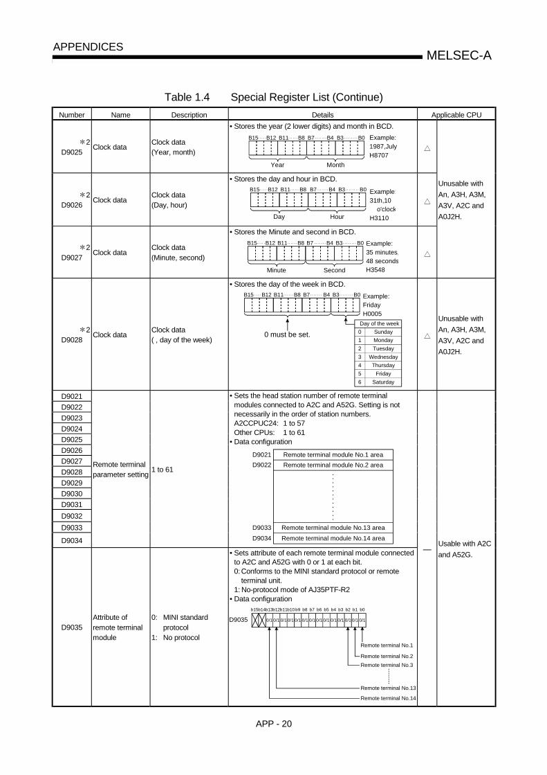
APP - 20
MELSEC-AAPPENDICES
Table 1.4 Special Register List (Continue)Number Name Description Details Applicable CPU
2D9025
Clock data Clock data(Year, month)
• Stores the year (2 lower digits) and month in BCD.
Year Month
Example:1987,JulyH8707
B11 B8 B7 B4 B3 B0B15 B12. . . . . . . . . . . . . . . . . . . . . . . . . .
2D9026 Clock data
Clock data(Day, hour)
• Stores the day and hour in BCD.
Day Hour
B11 B8 B7 B4 B3 B0B15 B12. . . . . . . . . . . . . . . . . . . . . . . . . . Example:31th,10 o'clockH3110
2D9027
Clock dataClock data(Minute, second)
• Stores the Minute and second in BCD.
Minute Second
B11 B8 B7 B4 B3 B0B15 B12.. . . . . . . . . . . . . . . . . . . . . . . . . Example:35 minutes,48 secondsH3548
Unusable withAn, A3H, A3M,A3V, A2C andA0J2H.
2D9028
Clock data Clock data( , day of the week)
• Stores the day of the week in BCD.B11 B8 B7 B4 B3 B0B15 B12.. . . . . . . . . . . . . . . . . . . . . . . .
0 must be set.Day of the week
SundayMondayTuesday
WednesdayThursday
FridaySaturday
0123456
Example:FridayH0005
Unusable withAn, A3H, A3M,A3V, A2C andA0J2H.
D9021D9022D9023D9024D9025D9026D9027D9028D9029D9030D9031D9032D9033
D9034
Remote terminalparameter setting 1 to 61
• Sets the head station number of remote terminalmodules connected to A2C and A52G. Setting is notnecessarily in the order of station numbers.A2CCPUC24: 1 to 57Other CPUs: 1 to 61
• Data configuration
D9021D9022
D9033D9034
Remote terminal module No.1 areaRemote terminal module No.2 area
. . .
. . .
. . .
. . .
Remote terminal module No.13 areaRemote terminal module No.14 area
D9035Attribute ofremote terminalmodule
0: MINI standardprotocol
1: No protocol
• Sets attribute of each remote terminal module connectedto A2C and A52G with 0 or 1 at each bit.0: Conforms to the MINI standard protocol or remote
terminal unit.1: No-protocol mode of AJ35PTF-R2
• Data configuration
Remote terminal No.1
Remote terminal No.2Remote terminal No.3
Remote terminal No.13
Remote terminal No.14
b11 b8 b7 b4 b3 b0b15 b12b14b13 b10 b9 b6 b5 b2 b1
0/1 0/1 0/1 0/1 0/1 0/1 0/1 0/1 0/1 0/1 0/1 0/1 0/1 0/1D9035
......
..
—Usable with A2Cand A52G.
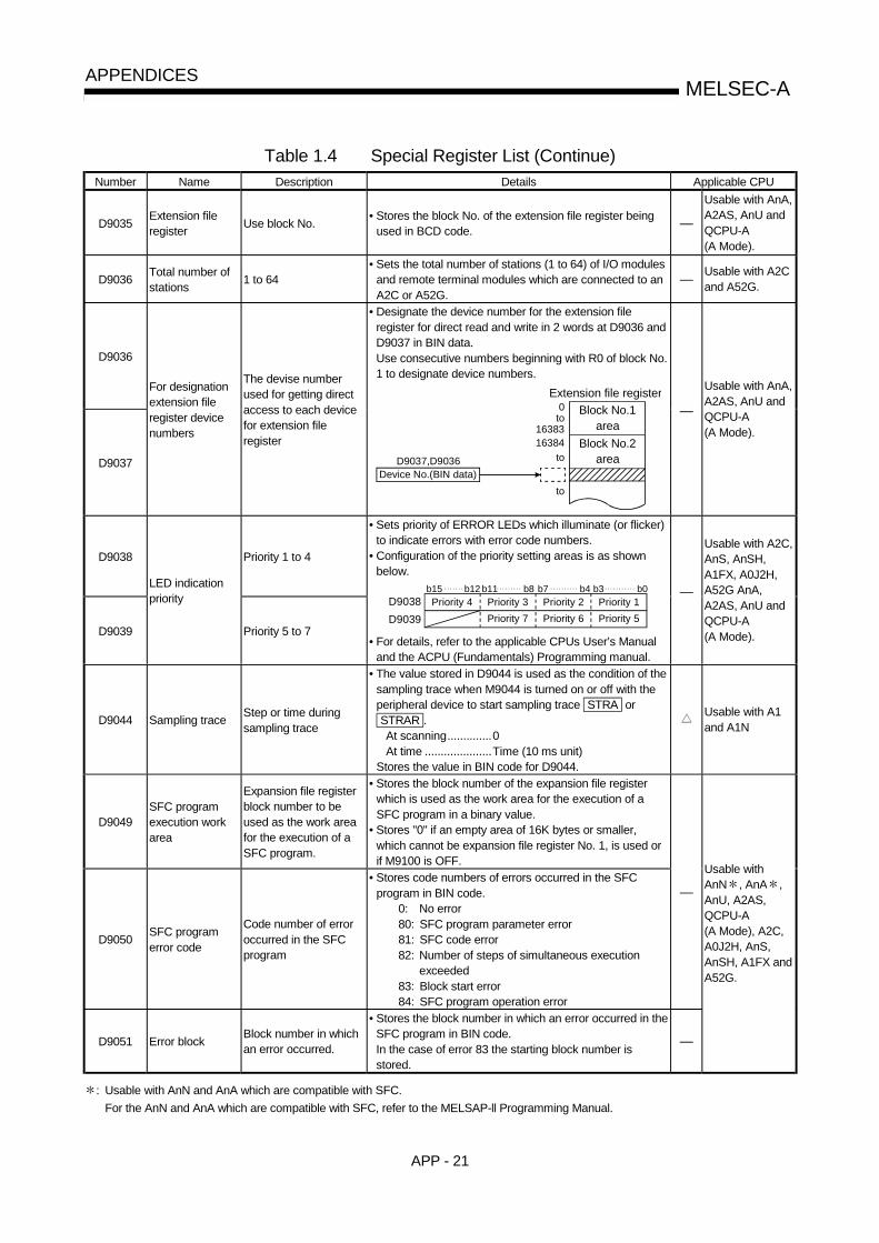
APP - 21
MELSEC-AAPPENDICES
Table 1.4 Special Register List (Continue)Number Name Description Details Applicable CPU
D9035 Extension fileregister Use block No. • Stores the block No. of the extension file register being
used in BCD code. —
Usable with AnA,A2AS, AnU andQCPU-A(A Mode).
D9036 Total number ofstations 1 to 64
• Sets the total number of stations (1 to 64) of I/O modulesand remote terminal modules which are connected to anA2C or A52G.
— Usable with A2Cand A52G.
D9036
D9037
For designationextension fileregister devicenumbers
The devise numberused for getting directaccess to each devicefor extension fileregister
• Designate the device number for the extension fileregister for direct read and write in 2 words at D9036 andD9037 in BIN data.Use consecutive numbers beginning with R0 of block No.1 to designate device numbers.
Block No.1area
Extension file register0
1638316384
Device No.(BIN data)D9037,D9036
Block No.2area
to
to
to —
Usable with AnA,A2AS, AnU andQCPU-A(A Mode).
D9038 Priority 1 to 4
D9039
LED indicationpriority
Priority 5 to 7
• Sets priority of ERROR LEDs which illuminate (or flicker)to indicate errors with error code numbers.
• Configuration of the priority setting areas is as shownbelow.
Priority 4D9038D9039
b15 . . . . . . . b12 . . . . . . . . .b11 b8 . . . . . . . . . .b7 b4 . . . . . . . . . . .b3 b0Priority 3 Priority 2 Priority 1
Priority 6Priority 7 Priority 5
• For details, refer to the applicable CPUs User’s Manualand the ACPU (Fundamentals) Programming manual.
—
Usable with A2C,AnS, AnSH,A1FX, A0J2H,A52G AnA,A2AS, AnU andQCPU-A(A Mode).
D9044 Sampling trace Step or time duringsampling trace
• The value stored in D9044 is used as the condition of thesampling trace when M9044 is turned on or off with theperipheral device to start sampling trace STRA or STRAR .
At scanning..............0At time .....................Time (10 ms unit)
Stores the value in BIN code for D9044.
Usable with A1and A1N
D9049SFC programexecution workarea
Expansion file registerblock number to beused as the work areafor the execution of aSFC program.
• Stores the block number of the expansion file registerwhich is used as the work area for the execution of aSFC program in a binary value.
• Stores "0" if an empty area of 16K bytes or smaller,which cannot be expansion file register No. 1, is used orif M9100 is OFF.
D9050 SFC programerror code
Code number of erroroccurred in the SFCprogram
• Stores code numbers of errors occurred in the SFCprogram in BIN code.
0: No error80: SFC program parameter error81: SFC code error82: Number of steps of simultaneous execution
exceeded83: Block start error84: SFC program operation error
—
D9051 Error block Block number in whichan error occurred.
• Stores the block number in which an error occurred in theSFC program in BIN code.In the case of error 83 the starting block number isstored.
—
Usable withAnN , AnA ,AnU, A2AS,QCPU-A(A Mode), A2C,A0J2H, AnS,AnSH, A1FX andA52G.
: Usable with AnN and AnA which are compatible with SFC.For the AnN and AnA which are compatible with SFC, refer to the MELSAP-ll Programming Manual.
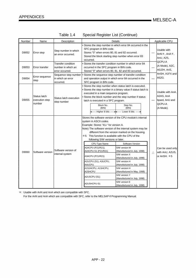
APP - 22
MELSEC-AAPPENDICES
Table 1.4 Special Register List (Continue)Number Name Description Details Applicable CPU
D9052 Error stepStep number in whichan error occurred.
• Stores the step number in which error 84 occurred in theSFC program in BIN code.Stores "0" when errors 80, 81 and 82 occurred.Stored the block starting step number when error 83occurred.
—
D9053 Error transferTransfer conditionnumber in which anerror occurred.
• Stores the transfer condition number in which error 84occurred in the SFC program in BIN code.Stored "0" when errors 80, 81, 82 and 83 occurred.
—
D9054 Error sequencestep
Sequence step numberin which an erroroccurred.
• Stores the sequence step number of transfer conditionand operation output in which error 84 occurred in theSFC program in BIN code.
—
Usable withAnN , AnA ,AnU, A2S,QCPU-A(A Mode), A2C,A0J2H, AnS,AnSH, A1FX andA52G.
D9055Status latchexecution stepnumber
Status latch executionstep number
• Stores the step number when status latch is executed.• Stores the step number in a binary value if status latch is
executed in a main sequence program.• Stores the block number and the step number if status
latch is executed in a SFC program.
Block No.(BIN)
Step No.(BIN)
Higher 8 bits Lower 8 bits
—
Usable with AnA,A2AS, AnAbpard, AnU andQCPU-A(A Mode).
Stores the software version of the CPU module's internalsystem in ASCII codes.Example: Stores "41H" for version A.Note) The software version of the internal system may be
different from the version marked on the housing.5: This function is available with the CPU of the
following S/W versions or later.CPU Type Name Software Version
A2ACPU (P21/R21),A2ACPU-S1 (P21/R21)
S/W version W(Manufactured in July, 1998)
A3ACPU (P21/R21)S/W version X(Manufactured in July, 1998)
A2UCPU (S1), A3UCPU,A4UCPU
S/W version H(Manufactured in July, 1998)
A1SJHCPU, A1SHCPU,A2SHCPU
S/W version H(Manufactured in May, 1998)
A2USCPU (S1)S/W version Y(Manufactured in July, 1998)
A2USHCPU-S1S/W version E(Manufactured in July, 1998)
D9060 Software version Software version ofinternal system
Can be used onlywith AnU, A2US,or AnSH. 5
: Usable with AnN and AnA which are compatible with SFC.For the AnN and AnA which are compatible with SFC, refer to the MELSAP-ll Programming Manual.
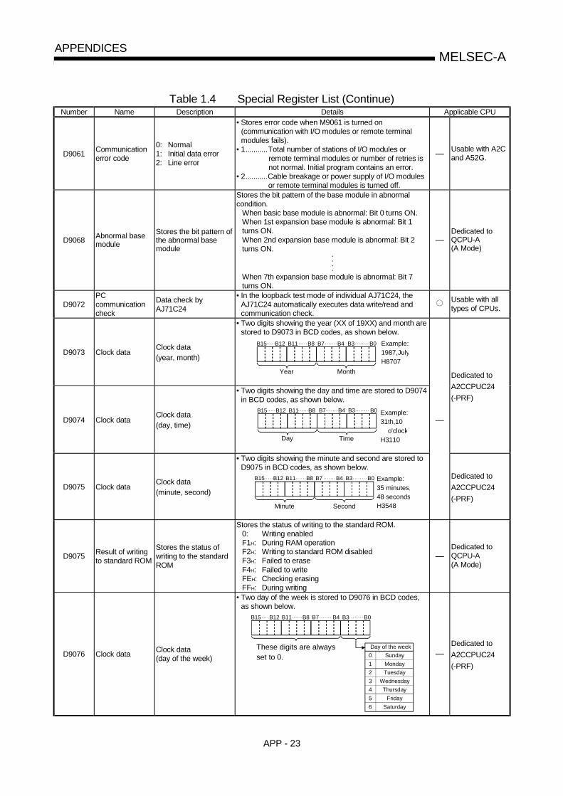
APP - 23
MELSEC-AAPPENDICES
Table 1.4 Special Register List (Continue)Number Name Description Details Applicable CPU
D9061 Communicationerror code
0: Normal1: Initial data error2: Line error
• Stores error code when M9061 is turned on(communication with I/O modules or remote terminalmodules fails).
• 1...........Total number of stations of I/O modules orremote terminal modules or number of retries isnot normal. Initial program contains an error.
• 2...........Cable breakage or power supply of I/O modulesor remote terminal modules is turned off.
— Usable with A2Cand A52G.
D9068 Abnormal basemodule
Stores the bit pattern ofthe abnormal basemodule
Stores the bit pattern of the base module in abnormalcondition.
When basic base module is abnormal: Bit 0 turns ON.When 1st expansion base module is abnormal: Bit 1turns ON.When 2nd expansion base module is abnormal: Bit 2turns ON.
····When 7th expansion base module is abnormal: Bit 7turns ON.
—Dedicated toQCPU-A(A Mode)
D9072PCcommunicationcheck
Data check byAJ71C24
• In the loopback test mode of individual AJ71C24, theAJ71C24 automatically executes data write/read andcommunication check.
Usable with alltypes of CPUs.
D9073 Clock data Clock data(year, month)
• Two digits showing the year (XX of 19XX) and month arestored to D9073 in BCD codes, as shown below.
Year Month
Example:1987,JulyH8707
B11 B8 B7 B4 B3 B0B15 B12. . . . . . . . . . . . . . . . . . . . . . . . . .
D9074 Clock dataClock data(day, time)
• Two digits showing the day and time are stored to D9074in BCD codes, as shown below.
Day Time
B11 B8 B7 B4 B3 B0B15 B12.. . . . . . . . . . . . . . . . . . . . . . . . . Example:31th,10 o'clockH3110
Dedicated toA2CCPUC24(-PRF)
D9075 Clock data Clock data(minute, second)
• Two digits showing the minute and second are stored toD9075 in BCD codes, as shown below.
Minute Second
B11 B8 B7 B4 B3 B0B15 B12.. . . . . . . . . . . . . . . . . . . . . . . . . Example:35 minutes,48 secondsH3548
—
Dedicated toA2CCPUC24(-PRF)
D9075 Result of writingto standard ROM
Stores the status ofwriting to the standardROM
Stores the status of writing to the standard ROM.0: Writing enabledF1H: During RAM operationF2H: Writing to standard ROM disabledF3H: Failed to eraseF4H: Failed to writeFEH: Checking erasingFFH: During writing
—Dedicated toQCPU-A(A Mode)
D9076 Clock data Clock data(day of the week)
• Two day of the week is stored to D9076 in BCD codes,as shown below.
B11 B8 B7 B4 B3 B0B15 B12. . . . . . . . . . . . . . . . . . . . . . . . .
These digits are alwaysset to 0.
Day of the weekSundayMondayTuesday
WednesdayThursday
FridaySaturday
0123456
—Dedicated toA2CCPUC24(-PRF)

APP - 24
MELSEC-AAPPENDICES
Table 1.4 Special Register List (Continue)Number Name Description Details Applicable CPU
D9076 Status of writingto standard ROM
Stores the status ofwriting(enabled/disabled) tothe standard ROM
Stores the status of writing (enabled/disabled) to thestandard ROM.Statuses of DIP switch 3 and M9073
0: SW3 is OFF, M9073 is OFF/ON1: SW3 is ON, M9073 is OFF2: SW3 is ON, M9073 is ON
—Dedicated toQCPU-A(A Mode)
D9077Sequenceaccumulationtimemeasurement
Accumulation timesetting
• Stores the accumulation time used by M9077.Setting range: 1 to 255ms (Default: 5ms) When the value other than 1 to 255 ms is designated,the value in D9077 is reset to 0.
—Dedicated toQCPU-A(A Mode)
Stores the number of remaining instructions(RIRD/RIWT/RISEND/RIRCV) being executablesimultaneously at one scan.(With QCUP-A or AnUCPU)
Number of remaining instructions being executable = 10– Number of instructions executed simultaneously(With AnSHCPU)Number of remaining instructions being executable = 64– Number of instructions executed simultaneously6: This function is available with the CPU of the
following S/W versions or later.CPU Type Name Software Version
Q02CPU-A, Q02HCPU-A,Q06HCPU-AA1SJHCPU, A1SHCPU,A2SHCPU
Available with all versions
A2UCPU (S1), A3UCPU,A4UCPU
S/W version Q(Manufactured in July, 1999)
A2USCPU (S1)S/W version E(Manufactured in July, 1999)
A2USHCPU-S1S/W version L(Manufactured in July, 1999)
D9080
Number ofexecutable CC-Link dedicatedinstructions
Stores the number ofremaining CC-Linkdedicated instructionsbeing executable
Can be used onlywith AnU, A2US,QCPU-A(A Mode) orAnSH 6
D9081
Number ofvacantregistration areasforcommunicationrequests
0 to 32
• Stores the number of vacant registration areas forcommunication requests executed to remote terminalmodules connected to MINI (S3) link module, A2C andA52G.
—
Usable with AnA,A2AS, QCPU-A(A Mode), AnU,A2C and A52G.
D9082 Final connectedstation number
Final connected stationnumber
• Stores the final station number of remote I/O modulesand remote terminal modules connected to A2C andA52G.
— Usable with A2Cand A52G.
D9085 Time check time 1 s to 65535 s
• Sets the time check time of the data link instructions( ZNRD , ZNWR ) for the MELSECNET/10.
• Setting range: 1 s to 65535 s (1 to 65535)• Setting unit: 1 s• Default value: 10 s (If 0 has been set, default 10 s is
applied)
—
Usable with AnUand A2AS,QCPU-A(A Mode)
D9090
Microcomputersubroutine inputdata area headdevice number
Depends on the micro-computer programpackage to be used.
• For details, refer to the manual of each microcomputerprogram package.
Unusable withAnA, A2AS,QCPU-A (AMode) and AnU.
Instruction error Instruction error detailnumber • Stores the detail code of cause of an instruction error. —
Usable with AnA,A2AS, QCPU-A(A Mode),AnAboard and AnU.
D9091Microcomputersubroutine callerror code
Depends on the micro-computer programpackage to be used.
• For details, refer to the manual of each microcomputerprogram package.
Unusable withAnA, A2AS,QCPU-A(A Mode),AnAboard and AnU.

APP - 25
MELSEC-AAPPENDICES
Table 1.4 Special Register List (Continue)Number Name Description Details Applicable CPU
D9091SFC programdetail errornumber
Detail error number ofthe error whichoccurred in a SFCprogram
• Stores the detail error number of the error occurred in aSFC program in a binary value. —
Usable with AnA,A2AS, QCPU-A(A Mode),AnAboard and AnU.
2 3D9094
Changed I/Omodule headaddress
Changed I/O modulehead address
• Stores upper 2 digits of the head I/O address of I/Omodules to be loaded or unloaded during online mode inBIN code.Example) Input module X2F0 H2F
—
Unusable withAnA, A2AS,QCPU-A(A Mode),AnAboard and AnU.
Operation stateof the A3VTSsystem andA3VCPU
Stores operation with 4hexadecimal digits.
• Monitors operation state of the A3VTS system and theA3VCPU.
B15 B12 B8 B4 B0D9095
CPU A CPU B CPU C
Data(H)
A RUN
STOPPAUSE
BCDE
Operation state
STEP-RUN
ERROR
0 RUN
STOPPAUSE
1234
STEP-RUN
WAITERROR
NO RIGHT OFOPERATION
56
7
System operation state
Data(H) Operation state
STAND-BY
—Dedicated toA3V.
D9095
Dip switchinformation
Dip switch information
• Dip switch information of CPU module is stored asfollows.
0:ON 1:OFF
B4 B3 B0B2 B1
SW1
SW2
SW3
SW4
SW5
B15 to
D9095 0—
Usable wtihQCPU-A(A mode) only.
D9096 A3VCPU ASelf-check error
Self-check error code• Error code of self-check error on CPU A is stored in BIN
code.• Cleared when D9008 of CPU A is cleared.
—Dedicated toA3V.
D9097 A3VCPU BSelf-check error
Self-check error code• Error code of self-check error on CPU B is stored in BIN
code.• Cleared when D9008 of CPU B is cleared.
—Dedicated toA3V.
D9098 A3VCPU CSelf-check error
Self-check error code• Error code of self-check error on CPU C is stored in BIN
code.• Cleared when D9008 of CPU C is cleared.
—Dedicated toA3V.
D9099 A3VTUSelf-check error
Self-check error code • Error code of self-check error on A3VTU is stored in BINcode. —
Dedicated toA3V.
: Usable with AnN and AnA which are compatible with SFC.For the AnN and AnA which are compatible with SFC, refer to the MELSAP-ll Programming Manual.
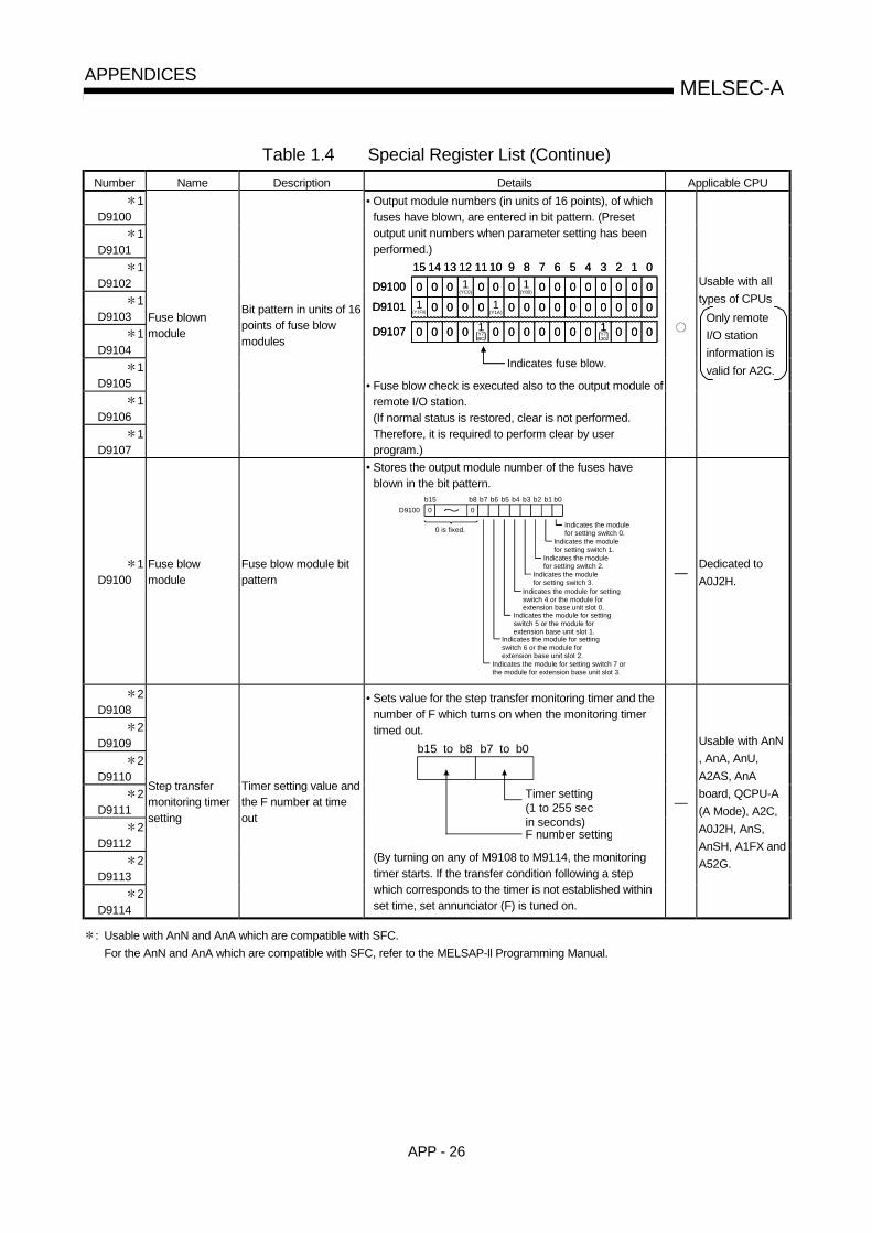
APP - 26
MELSEC-AAPPENDICES
Table 1.4 Special Register List (Continue)Number Name Description Details Applicable CPU
1D9100
1D9101
1D9102
1D9103
1D9104
1D9105
1D9106
1D9107
Fuse blownmodule
Bit pattern in units of 16points of fuse blowmodules
• Output module numbers (in units of 16 points), of whichfuses have blown, are entered in bit pattern. (Presetoutput unit numbers when parameter setting has beenperformed.)
D9100
D9101
D9107
15 14 12 1113 10 9 8 6 5 4 3 2 1 07
0 0 00 0 0 1(Y80) 0 0 0 0 0 0 00
0 0 00 1(Y1A) 0 0 0 0 0 0 0 0 00
0 0 00 0 0 0 0 0 0 0 0 00
Indicates fuse blow.
D9100
D9101
D9107
15 14 12 1113 10 9 8 6 5 4 3 2 1 07
0 0 1(YC0) 00 0 0 0 0 0 0 0 0 00
1(Y1F0) 0 0 00 0 0 0 0 0 0 0 0 00
0 0 00 0 0 0 0 0 0 0 0 001Y7BC
11Y730
• Fuse blow check is executed also to the output module ofremote I/O station.(If normal status is restored, clear is not performed.Therefore, it is required to perform clear by userprogram.)
Usable with alltypes of CPUs
Only remoteI/O stationinformation isvalid for A2C.
1D9100
Fuse blowmodule
Fuse blow module bitpattern
• Stores the output module number of the fuses haveblown in the bit pattern.
0 0b15
D9100b8 b7 b6 b5 b4 b3 b2 b1
0 is fixed. Indicates the modulefor setting switch 0.
Indicates the modulefor setting switch 1.
Indicates the modulefor setting switch 2.
Indicates the modulefor setting switch 3.
Indicates the module for setting switch 4 or the module forextension base unit slot 0.
Indicates the module for setting switch 5 or the module forextension base unit slot 1.
Indicates the module for setting switch 6 or the module forextension base unit slot 2.
Indicates the module for setting switch 7 or the module for extension base unit slot 3.
b0
—Dedicated toA0J2H.
2D9108
2D9109
2D9110
2D9111
2D9112
2D9113
2D9114
Step transfermonitoring timersetting
Timer setting value andthe F number at timeout
• Sets value for the step transfer monitoring timer and thenumber of F which turns on when the monitoring timertimed out.
b15 to b8 b7 to b0
Timer setting(1 to 255 secin seconds)F number setting
(By turning on any of M9108 to M9114, the monitoringtimer starts. If the transfer condition following a stepwhich corresponds to the timer is not established withinset time, set annunciator (F) is tuned on.
—
Usable with AnN, AnA, AnU,A2AS, AnAboard, QCPU-A(A Mode), A2C,A0J2H, AnS,AnSH, A1FX andA52G.
: Usable with AnN and AnA which are compatible with SFC.For the AnN and AnA which are compatible with SFC, refer to the MELSAP-ll Programming Manual.

APP - 27
MELSEC-AAPPENDICES
Table 1.4 Special Register List (Continue)Number Name Description Details Applicable CPU
1D9116
1D9117
1D9118
1D9119
1D9120
1D9121
1D9122
1D9123
I/O module verifyerror
Bit pattern in units of 16points of verify errorunits
• When I/O modules, of which data are different from thoseentered at power-on, have been detected, the I/O unitnumbers (in units of 16 points) are entered in bit pattern.(Preset I/O unit numbers when parameter setting hasbeen performed.)
D9116
D9117
D9123
15 14 12 1113 10 9 8 6 5 4 3 2 1 07
0 0 00 0 0 0 0 0 0 0 0 00
0 0 00 0 0 0 0 0 0 0 0 00
0 00 0 0 0 0 0 0 0 0 00
Indicates I/O module verify error.
0
0
001XY7E0
1XY180
1XY0
• I/O module verify check is executed also to remote I/Ostation modules.(If normal status is restored, clear is not performed.Therefore, it is required to perform clear by userprogram.)
Usable with alltypes of CPUs
Only remoteI/O stationinformation isvalid for A2C.
1D9116
I/O moduleverification error
Bit pattern ofverification errormodule
• When an I/O module different from the I/O module dataregistered during power-on is detected, this registerindicates the bit pattern of the I/O module number.
0 0b15
D9116b8 b7 b6 b5 b4 b3 b2 b1
0 is fixed.Indicates the modulefor setting switch 0.
Indicates the modulefor setting switch 1.
Indicates the modulefor setting switch 2.
Indicates the modulefor setting switch 3.
Indicates the module for setting switch 4 or the module forextension base unit slot 0.
Indicates the module for setting switch 5 or the module forextension base unit slot 1.
Indicates the module for setting switch 6 or the module forextension base unit slot 2.
Indicates the module for setting switch 7 or the module for extension base unit slot 3.
b0
—Dedicated toA0J2H.
D9124Annunciatordetectionquantity
Annunciator detectionquantity
• When one of F0 to 255 (F0 to 2047 for AnA and AnU) isturned on by SET F 1 is added to the contents ofD9124. When RST F or LEDR instruction is executed,1 is subtracted from the contents of D9124. (If theINDICATOR RESET switch is provided to the CPU,pressing the switch can execute the same processing.)
• Quantity, which has been turned on by SET F is storedinto D9124 in BIN code. The quantity turned on with SET F is stored up to “8.”
Usable with alltypes of CPUs.
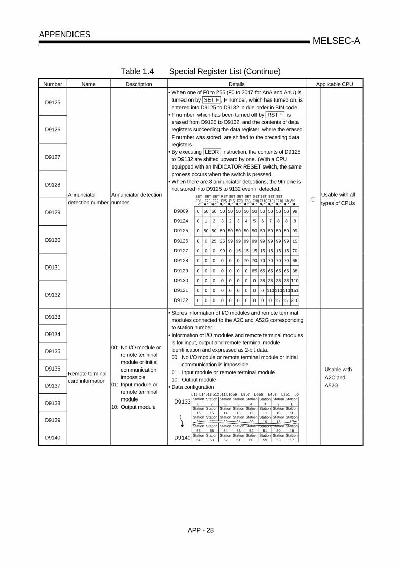
APP - 28
MELSEC-AAPPENDICES
Table 1.4 Special Register List (Continue)Number Name Description Details Applicable CPU
D9125
D9126
D9127
D9128
D9129
D9130
D9131
D9132
Annunciatordetection number
Annunciator detectionnumber
• When one of F0 to 255 (F0 to 2047 for AnA and AnU) isturned on by SET F , F number, which has turned on, isentered into D9125 to D9132 in due order in BIN code.
• F number, which has been turned off by RST F , iserased from D9125 to D9132, and the contents of dataregisters succeeding the data register, where the erasedF number was stored, are shifted to the preceding dataregisters.
• By executing LEDR instruction, the contents of D9125to D9132 are shifted upward by one. (With a CPUequipped with an INDICATOR RESET switch, the sameprocess occurs when the switch is pressed.
• When there are 8 annunciator detections, the 9th one isnot stored into D9125 to 9132 even if detected.
SETF50
SETF25
SETF99
RSTF25
SETF15
SETF70
SETF65
SETF38
SETF110
SETF151
SETF210 LEDR
50D9009 50 50 50 50 50 50 50 50 50 50 990
2D9124 1 3 2 3 4 5 6 7 8 8 80
50D9125 50 50 50 50 50 50 50 50 50 50 990
25D9126 0 25 99 99 99 99 99 99 99 99 150
0D9127 0 99 0 15 15 15 15 15 15 15 700
0D9128 0 0 0 0 70 70 70 70 70 70 650
0D9132 0 0 0 0 0 0 0 0 151 151 2100
0D9129 0 0 0 0 0 65 65 65 65 65 380
0D9130 0 0 0 0 0 0 38 38 38 38 1100
0D9131 0 0 0 0 0 0 0 110 110 110 1510
Usable with alltypes of CPUs
D9133
D9134
D9135
D9136
D9137
D9138
D9139
D9140
Remote terminalcard information
00: No I/O module orremote terminalmodule or initialcommunicationimpossible
01: Input module orremote terminalmodule
10: Output module
• Stores information of I/O modules and remote terminalmodules connected to the A2C and A52G correspondingto station number.
• Information of I/O modules and remote terminal modulesis for input, output and remote terminal moduleidentification and expressed as 2-bit data.00: No I/O module or remote terminal module or initial
communication is impossible.01: Input module or remote terminal module10: Output module
• Data configuration
Station51
Station50
Station17
Station18
Station20
Station21
Station22
Station23
Station24
D9133
D9140
b15 b14b13 b12b11 b10b9 b8b7 b6b5 b4b3 b2b1 b0Station
8
Station64
Station7
Station6
Station5
Station4
Station3
Station2
Station1
Station9
Station10
Station11
Station12
Station13
Station14
Station15
Station16
Station63
Station62
Station61
Station60
Station59
Station58
Station57
Station49
Station52
Station53
Station54
Station55
Station56
Station19
Usable withA2C andA52G
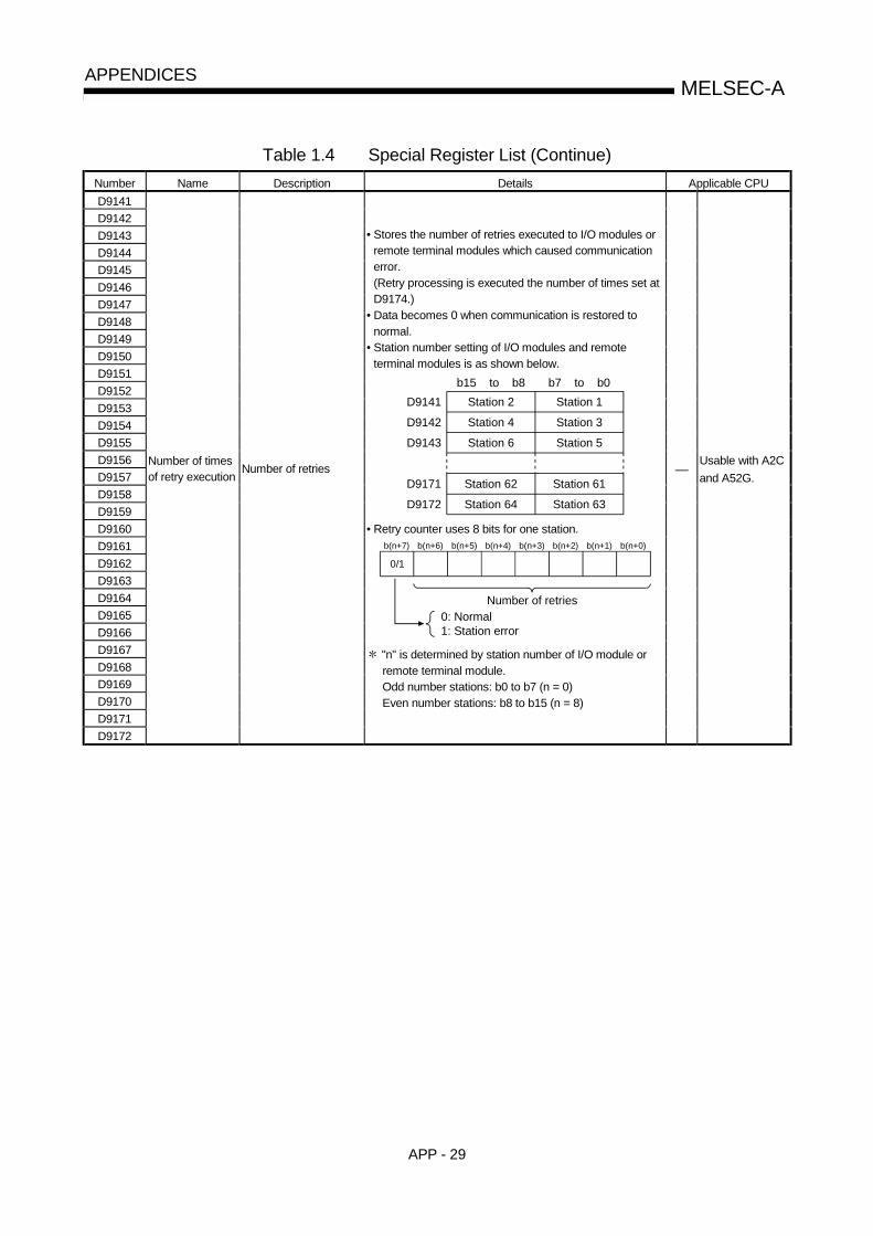
APP - 29
MELSEC-AAPPENDICES
Table 1.4 Special Register List (Continue)Number Name Description Details Applicable CPUD9141D9142D9143D9144D9145D9146D9147D9148D9149D9150D9151D9152D9153D9154D9155D9156D9157D9158D9159D9160D9161D9162D9163D9164D9165D9166D9167D9168D9169D9170D9171D9172
Number of timesof retry execution
Number of retries
• Stores the number of retries executed to I/O modules orremote terminal modules which caused communicationerror.(Retry processing is executed the number of times set atD9174.)
• Data becomes 0 when communication is restored tonormal.
• Station number setting of I/O modules and remoteterminal modules is as shown below.
b15 to b8 b7 to b0D9141 Station 2
Station 4
Station 6
Station 62
Station 64
Station 1
Station 3
Station 5
Station 61
Station 63
D9142
D9171
D9172
D9143
• Retry counter uses 8 bits for one station.b(n+7)
0/1
Number of retries
b(n+6) b(n+5) b(n+4) b(n+3) b(n+2) b(n+1) b(n+0)
0: Normal1: Station error
"n" is determined by station number of I/O module orremote terminal module.Odd number stations: b0 to b7 (n = 0)Even number stations: b8 to b15 (n = 8)
—Usable with A2Cand A52G.

APP - 30
MELSEC-AAPPENDICES
Table 1.4 Special Register List (Continue)Number Name Description Details Applicable CPU
Mode setting0 Auto-
maticonlinereturnenabled
• When an I/O module or a remote terminalmodule caused communication error, thestation is placed offline.
• Communication with normal stations iscontinued.
• The station recovering from acommunication error automaticallyresumes communication.
1 Auto-maticonlinereturndisabled
• When an I/O module or a remote terminalmodule caused communication error, thestation is placed offline.
• Communication with normal stations iscontinued.
• Though a faulty station returned to normal,communication is not restored unless thestation module is restarted.
2 Trans-missionstop atonlineerror
• When an I/O module or a remote terminalmodule caused communication error,communication with all stations is stopped.
• Though a faulty station returned to normal,communication is not restored unless thestation module is restarted.
D9173 Mode setting
0: Automatic onlinereturn enabled
1: Automatic onlinereturn disabled
2: Transmission stopat online error
3: Line check
3 Linecheck
• Checks hardware and connecting cablesof I/O modules and remote terminalmodules.
— Usable with A2Cand A52G.
D9174Setting of thenumber of retries
Number of retries
• Sets the number of retries executed to I/O modules andremote terminal modules which caused communicationerror.
• Set for 5 times at power on.• Set range: 0 to 32• If communication with an I/O module or a remote terminal
module is not restored to normal after set number ofretries, such module is regarded as a faulty station.
— Usable with A2Cand A52G.
D9175 Line error retrycounter
Number of retries
• Stores the number of retries executed at line error (timeout).
• Data becomes 0 when line is restored to normal andcommunication with I/O modules and remote terminalmodules is resumed.
— Usable with A2Cand A52G.
D9180D9181D9182D9183D9184D9185D9186D9187D9188D9189D9190D9191D9192D9193
Remote terminalmodule errornumber
• Stores error code of a faulty remote terminal modulewhen M9060 is turned on.
• The error code storage areas for each remote terminalmodule are as shown below.
D9180
D9181
D9192
D9193
Remote terminal module No.1
D9182
...
Remoteterminalmodulenumbersfrom 1 to 14are set withD9020 toD9034.
Remote terminal module No.2
Remote terminal module No.3
Remote terminal module No.13
Remote terminal module No.14
• Error code is cleared in the following cases.• When the RUN key switch is moved from STOP to RUN.
(D9180 to D9183 are all cleared.)• When Yn4 of each remote terminal is set from OFF to
ON.
— Usable with A2Cand A52G.
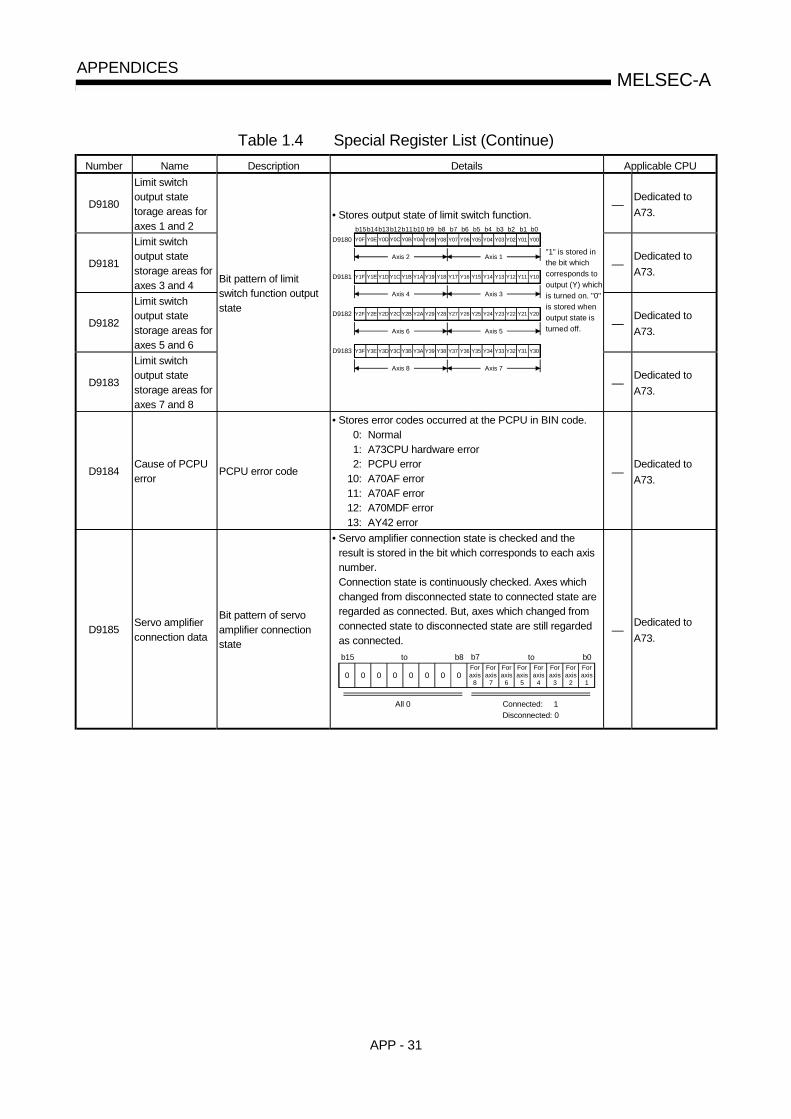
APP - 31
MELSEC-AAPPENDICES
Table 1.4 Special Register List (Continue)Number Name Description Details Applicable CPU
D9180
Limit switchoutput statetorage areas foraxes 1 and 2
—Dedicated toA73.
D9181
Limit switchoutput statestorage areas foraxes 3 and 4
—Dedicated toA73.
D9182
Limit switchoutput statestorage areas foraxes 5 and 6
—Dedicated toA73.
D9183
Limit switchoutput statestorage areas foraxes 7 and 8
Bit pattern of limitswitch function outputstate
• Stores output state of limit switch function.b15Y0F
b14b13b12b11b10 b9 b8 b7 b6 b5 b4 b3 b2 b1 b0Y0E Y0D Y0C Y0B Y0A Y09 Y08 Y07 Y06 Y05 Y04 Y03 Y02 Y01 Y00
Axis 1Axis 2
D9180
Y1F Y1E Y1D Y1C Y1B Y1A Y19 Y18 Y17 Y16 Y15 Y14 Y13 Y12 Y11 Y10
Axis 3Axis 4
D9181
Y2F Y2E Y2D Y2C Y2B Y2A Y29 Y28 Y27 Y26 Y25 Y24 Y23 Y22 Y21 Y20
Axis 5Axis 6
D9182
Y3F Y3E Y3D Y3C Y3B Y3A Y39 Y38 Y37 Y36 Y35 Y34 Y33 Y32 Y31 Y30
Axis 7Axis 8
D9183
"1" is stored inthe bit whichcorresponds tooutput (Y) whichis turned on. "0"is stored whenoutput state isturned off.
—Dedicated toA73.
D9184Cause of PCPUerror
PCPU error code
• Stores error codes occurred at the PCPU in BIN code. 0: Normal 1: A73CPU hardware error 2: PCPU error10: A70AF error11: A70AF error12: A70MDF error13: AY42 error
—Dedicated toA73.
D9185 Servo amplifierconnection data
Bit pattern of servoamplifier connectionstate
• Servo amplifier connection state is checked and theresult is stored in the bit which corresponds to each axisnumber.Connection state is continuously checked. Axes whichchanged from disconnected state to connected state areregarded as connected. But, axes which changed fromconnected state to disconnected state are still regardedas connected.b15 b8 b7 b0
0 0 0 0 0 0 0 0Foraxis
8
Foraxis
7
Foraxis
6
Foraxis
5
Foraxis
4
Foraxis
3
Foraxis
2
Foraxis
1
All 0 Connected: 1Disconnected: 0
to to
—Dedicated toA73.
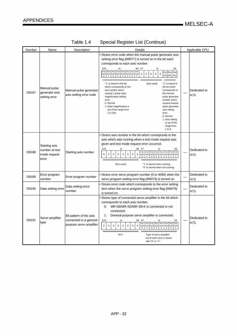
APP - 32
MELSEC-AAPPENDICES
Table 1.4 Special Register List (Continue)Number Name Description Details Applicable CPU
D9187Manual pulsegenerator axissetting error
Manual pulse generatoraxis setting error code
• Stores error code when the manual pulse generator axissetting error flag (M9077) is turned on in the bit eachcorresponds to each axis number.b15 b8 b7 b0
0 0 0 0 0Foraxis
8
Foraxis
7
Foraxis
6
Foraxis
5
Foraxis
4
Foraxis
3
Foraxis
2
Foraxis
1
ForP3
ForP2
ForP1
"1" is stored in the bitwhich corresponds to theaxis number whichcaused 1 pulse inputmagnification settingerror.0: Normal1: Input magnification is out of the range from 1 to 100.
(Not used) "1" is stored inthe bit which corresponds tothe manualpulse generatornumber whichcaused manualpulse generatoraxis settingerror.0: Normal1: Axis setting is out of the range from 1 to 8.
toto
—Dedicated toA73.
D9188
Starting axisnumber at testmode requesterror
Starting axis number
• Stores axis number in the bit which corresponds to theaxis which was running when a test mode request wasgiven and test mode request error occurred.b15 b8 b7 b0
0 0 0 0 0 0 0 0Foraxis
8
Foraxis
7
Foraxis
6
Foraxis
5
Foraxis
4
Foraxis
3
Foraxis
2
Foraxis
1
(Not used) "1" is stored when running."0" is stored when not running.
to to—
Dedicated toA73.
D9189 Error programnumber
Error program number • Stores error servo program number (0 to 4095) when theservo program setting error flag (M9079) is turned on. —
Dedicated toA73.
D9190 Data setting error Data setting errornumber
• Stores error code which corresponds to the error settingitem when the servo program setting error flag (M9079)is turned on.
—Dedicated toA73.
D9191 Servo amplifiertype
Bit pattern of the axisconnected to a general-purpose servo amplifier
• Stores type of connected servo amplifier in the bit whichcorresponds to each axis number.
0: MR-SB/MR-SD/MR-SB-K is connected or notconnected.
1: General-purpose servo amplifier is connected.b15 b8 b7 b0
0 0 0 0 0 0 0 0Foraxis
8
Foraxis
7
Foraxis
6
Foraxis
5
Foraxis
4
Foraxis
3
Foraxis
2
Foraxis
1
All 0 Type of servo amplifierset at each axis is storedwith "0" or "1".
to to —Dedicated toA73.

APP - 33
MELSEC-AAPPENDICES
Table 1.4 Special Register List (Continue)Number Name Description Details Applicable CPU
D9196
D9197
D9198
D9199
Faulty stationdetection
Bit pattern of the faultystation
• Bit which corresponds to faulty I/O module or remoteterminal module is set (1).(Bit which corresponds to a faulty station is set whennormal communication cannot be restored afterexecuting the number of retries set at D9174.)
• If automatic online return is enabled, bit whichcorresponds to a faulty station is reset (0) when thestation is restored to normal.
• Data configurationb15 b14 b13 b12 b11 b10 b9 b8 b7 b6 b5 b4 b3 b2 b1 b0
Stasion16
Address
D9197
D9198
D9199
D9196
1: Error0: Normal
Stasion32
Stasion48
Stasion64
Stasion15
Stasion31
Stasion47
Stasion63
Stasion14
Stasion30
Stasion46
Stasion62
Stasion13
Stasion29
Stasion45
Stasion61
Stasion12
Stasion28
Stasion44
Stasion60
Stasion11
Stasion27
Stasion43
Stasion59
Stasion10
Stasion26
Stasion42
Stasion58
Stasion9
Stasion25
Stasion41
Stasion57
Stasion8
Stasion24
Stasion40
Stasion56
Stasion7
Stasion23
Stasion39
Stasion55
Stasion6
Stasion22
Stasion38
Stasion54
Stasion5
Stasion21
Stasion37
Stasion53
Stasion4
Stasion20
Stasion36
Stasion52
Stasion3
Stasion19
Stasion35
Stasion51
Stasion2
Stasion18
Stasion34
Stasion50
Stasion1
Stasion17
Stasion33
Stasion49
—Usable with A2Cand A52G.
POINTS(1) Special registers are cleared when the PC is switched off or the RESET switch
is set to LATCH CLEAR or RESET. Data remains unchanged when the RUNkey switch is set to STOP.
(2) The above special registers marked 1 above are latched and their data willremain unchanged after normal status is restored. For this reason, use one ofthe following methods to clear the registers.(a) Method by user program
Insert the circuit shown at right intothe program and turn on the clearexecution command contact to clearthe contents of register.
Clear executioncommand
RST D9005
Special function register to be cleared
(b) Method by peripheral equipmentSet the register to "0" by changing the present value by the test function ofperipheral equipment or set to "0" by forced reset. For the operationprocedure, refer to the Instruction Manual for peripheral equipment.
(c) By moving the RESET key switch at the CPU front to the RESET position,the special register is set to "0".
(3) Data is written to special registers marked 2 above in the sequence program.(4) Data is written to special registers marked 3 above in test mode of the
peripheral equipment.

APP - 34
MELSEC-AAPPENDICES
Appendix 1.4 Special registers for link
The link special register stores the result of any error, etc. which may occur during datacommunication as a numeric value.By monitoring the link special register, any station number with an error or faultdiagnosis can be read.These special registers are applicable to all types of CPUs except the A3V.For description of the special registers for link for the A3V, refer to the A3VTS DataLink System User’s Manual.
(1) Link special registers only valid when the host station is the masterstation
Table 1.5 Link special RegisterNumber Name Description Details
Stores the execution result of the LRDP (word device read)instruction
D9200 LRDP processingresult
0: Normal2: LRDP instruction
setting fault3: Corresponding station
error4: LRDP cannot be
executed in thecorresponding station
• LRDP instruction setting fault:
• Corresponding station error:
• LRDP cannot be executed in thecorresponding station:
Faulty setting of the LRDP instruction constant, source,and/or destinationOne of the stations is notcommunicating.The specified station is aremote I/O station.
Stores the execution result of the LWTP (word device write)instruction.
D9201 LWTP processingresult
0: Normal2: LWTP instruction
setting fault3: Corresponding station
error4: LWTP cannot be
executed in thecorresponding station
• LWTP instruction setting fault:
• Corresponding station error:
• LWTP cannot be executed in thecorresponding station:
Faulty setting of the LWTP instruction constant, source,and/or destination.One of the stations is notcommunicating.The specified station is aremote I/O station.
D9204(Continue)
Link status
0: Data link in forward loop1: Data link in reverse loop2: Loopback in
forward/reversedirection
3: Loopback in forwarddirection
4: Loopback in reversedirection
5: Data link impossible
Stores the present path status of the data link.• Data link in forward loop
Masterstation
Station 1 Station 2 Station n
Forward loop Reverse loop
• Data link in reverse loop
Masterstation
Station 1 Station 2 Station n
Forward loop Reverse loop
• Loopback in forward/reverse loops
Masterstation Station 1 Station 2 Station n
Forward loopback Reverse loopback
Station 3
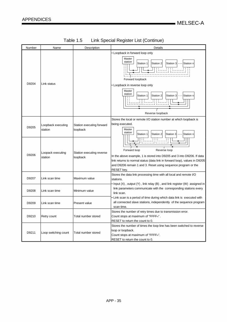
APP - 35
MELSEC-AAPPENDICES
Table 1.5 Link Special Register List (Continue)Number Name Description Details
D9204 Link status
• Loopback in forward loop only
Masterstation Station 1 Station 2 Station n
Forward loopback
Station 3
• Loopback in reverse loop only
Masterstation Station 1 Station 2 Station n
Reverse loopback
Station 3
D9205Loopback executingstation
Station executing forwardloopback
D9206Loopack executingstation
Station executing reverseloopback
Stores the local or remote I/O station number at which loopback isbeing executed.
Masterstation Station 1 Station 2 Station n
Forward loop Reverse loop
Station 3
In the above example, 1 is stored into D9205 and 3 into D9206. If datalink returns to normal status (data link in forward loop), values in D9205and D9206 remain 1 and 3. Reset using sequence program or theRESET key.
D9207 Link scan time Maximum value
D9208 Link scan time Minimum value
D9209 Link scan time Present value
Stores the data link processing time with all local and remote I/Ostations.• Input (X) , output (Y) , link relay (B) , and link register (W) assigned in
link parameters communicate with the corresponding stations everylink scan.
• Link scan is a period of time during which data link is executed withall connected slave stations, independently of the sequence programscan time.
D9210 Retry count Total number storedStores the number of retry times due to transmission error.Count stops at maximum of "FFFFH" .RESET to return the count to 0.
D9211 Loop switching count Total number stored
Stores the number of times the loop line has been switched to reverseloop or loopback.Count stops at maximum of "FFFFH".RESET to return the count to 0.

APP - 36
MELSEC-AAPPENDICES
Table 1.5 Link Special Register List (Continue)Number Name Description Details
D9212Local station operatingstatus
Stores the status of stations1 to 16
D9213Local station operatingstatus
Stores the status of stations17 to 32
D9214Local station operatingstatus
Stores the status of stations33 to 48
D9215Local station operatingstatus
Stores the status of stations49 to 64
Stores the local station numbers which are in STOP or PAUSE mode.
Devicenumber
Bit
D9212
D9213
D9214
D9215
L1
b15 b14 b13 b12 b11 b10 b9 b8 b7 b6 b5 b4 b3 b2 b1 b0
L16
L32
L48
L64
L15
L31
L47
L63
L14
L30
L46
L62
L13
L29
L45
L61
L12
L28
L44
L60
L11
L27
L43
L59
L10
L26
L42
L58
L9
L25
L41
L57
L8
L24
L40
L56
L7
L23
L39
L55
L6
L22
L38
L54
L5
L21
L37
L53
L4
L20
L36
L52
L3
L19
L35
L51
L2
L18
L34
L50
L17
L33
L49
When a local station is switched to STOP or PAUSE mode, the bitcorresponding to the station number in the register becomes "1" .Example : When station 7 switches to STOP mode, bit 6 in D9212
becomes "1" , and when D9212 is monitored, its value is "64(40H) " .
D9216Local station errordetection
Stores the status of stations1 to 16
D9217Local station errordetection
Stores the status of stations17 to 32
D9218Local station errordetection
Stores the status of stations33 to 48
D9219Local station errordetection
Stores the status of stations49 to 64
Stores the local station numbers which are in error.
Devicenumber
Bit
D9216
D9217
D9218
D9219
L1
b15 b14 b13 b12 b11 b10 b9 b8 b7 b6 b5 b4 b3 b2 b1 b0
L16
L32
L48
L64
L15
L31
L47
L63
L14
L30
L46
L62
L13
L29
L45
L61
L12
L28
L44
L60
L11
L27
L43
L59
L10
L26
L42
L58
L9
L25
L41
L57
L8
L24
L40
L56
L7
L23
L39
L55
L6
L22
L38
L54
L5
L21
L37
L53
L4
L20
L36
L52
L3
L19
L35
L51
L2
L18
L34
L50
L17
L33
L49
If a local station detects an error, the bit corresponding to the stationnumber becomes "1".Example : When station 6 and 12 detect an error, bits 5 and 11 in
D9216 become "1", and when D9216 is monitored, its valueis "2080 (820H)".
D9220
Local station parametermismatched or remotestation I/O assignmenterror
Stores the status of stations1 to 16
D9221
Local station parametermismatched or remotestation I/O assignmenterror
Stores the status of stations17 to 32.
D9222
Local station parametermismatched or remotestation I/O assignmenterror
Stores the status of stations33 to 48.
D9223
Local station parametermismatched or remotestation I/O assignmenterror
Stores the status of stations49 to 64.
Stores the local station numbers which contain mismatchedparameters or of remote station numbers for which incorrect I/Oassignment has been made.
Devicenumber
Bit
D9220
D9221
D9222
D9223
L/R1
b15 b14 b13 b12 b11 b10 b9 b8 b7 b6 b5 b4 b3 b2 b1 b0
L/R16
L/R32
L/R48
L/R64
L/R15
L/R31
L/R47
L/R63
L/R14
L/R30
L/R46
L/R62
L/R13
L/R29
L/R45
L/R61
L/R12
L/R28
L/R44
L/R60
L/R11
L/R27
L/R43
L/R59
L/R10
L/R26
L/R42
L/R58
L/R9
L/R25
L/R41
L/R57
L/R8
L/R24
L/R40
L/R56
L/R7
L/R23
L/R39
L/R55
L/R6
L/R22
L/R38
L/R54
L/R5
L/R21
L/R37
L/R53
L/R4
L/R20
L/R36
L/R52
L/R3
L/R19
L/R35
L/R51
L/R2
L/R18
L/R34
L/R50
L/R17
L/R33
L/R49
If a local station acting as the master station of tier three detects aparameter error or a remote station contains an invalid I/O assignment,the bit corresponding to the station number becomes "1" .Example: When local station 5 and remote I/O station 14 detect an
error, bits 4 and 13 in D9220 become "1" , and when D9220is monitored, its value is "8208 (2010H) " .

APP - 37
MELSEC-AAPPENDICES
Table 1.5 Link Special Register List (Continue)Number Name Description Details
D9224Initial communicationbetween local orremote I/O stations
Stores the status of stations1 to 16
D9225Initial communicationbetween local orremote I/O stations
Stores the status of stations17 to 32
D9226Initial communicationbetween local orremote I/O stations
Stores the status of stations33 to 48
D9227Initial communicationbetween local orremote I/O stations
Stores the status of stations49 to 64
Stores the local or remote station numbers while they arecommunicating the initial data with their relevant master station.
Devicenumber
Bit
b15 b14 b13 b12 b11 b10 b9 b8 b7 b6 b5 b4 b3 b2 b1 b0
D9224
D9225
D9226
D9227
L/R16L/R32L/R48L/R64
L/R15L/R31L/R47L/R63
L/R14L/R30L/R46L/R62
L/R13L/R29L/R45L/R61
L/R12L/R28L/R44L/R60
L/R11L/R27L/R43L/R59
L/R10L/R26L/R42L/R58
L/R9
L/R25L/R41L/R57
L/R8
L/R24L/R40L/R56
L/R7
L/R23L/R39L/R55
L/R6
L/R22L/R38L/R54
L/R5
L/R21L/R37L/R53
L/R4
L/R20L/R36L/R52
L/R3
L/R19L/R35L/R51
L/R2
L/R18L/R34L/R50
L/R1
L/R17L/R33L/R49
The bit corresponding to the station number which is currentlycommunicating the initial settings becomes "1" .Example: When stations 23 and 45 are communicating, bit 6 of D9225
and bit 12 of D9226 become "1", and when D9225 ismonitored, its value is "64 (40H)", and when D9226 ismonitored, its value is "4096 (1000H)"
D9228Local or remote I/Ostation error
Stores the status of stations1 to 16
D9229Local or remote I/Ostation error
Stores the status of stations17 to 32
D9230Local or remote I/Ostation error
Stores the status of stations33 to 48
D9231Local or remote I/Ostation error
Stores the status of stations49 to 64
Stores the local or remote station numbers which are in error.Devicenumber
Bit
b15 b14 b13 b12 b11 b10 b9 b8 b7 b6 b5 b4 b3 b2 b1 b0
D9228
D9229
D9230
D9231
L/R16L/R32L/R48L/R64
L/R15L/R31L/R47L/R63
L/R14L/R30L/R46L/R62
L/R13L/R29L/R45L/R61
L/R12L/R28L/R44L/R60
L/R11L/R27L/R43L/R59
L/R10L/R26L/R42L/R58
L/R9
L/R25L/R41L/R57
L/R8
L/R24L/R40L/R56
L/R7
L/R23L/R39L/R55
L/R6
L/R22L/R38L/R54
L/R5
L/R21L/R37L/R53
L/R4
L/R20L/R36L/R52
L/R3
L/R19L/R35L/R51
L/R2
L/R18L/R34L/R50
L/R1
L/R17L/R33L/R49
The bit corresponding to the station number with the error becomes "1"Example: When local station 3 and remote I/O station 14 have an
error, bits 2 and 13 of D9228 become "1", and when D9228is monitored, its value is "8196 (2004H)".
D9232Local or remote I/Ostation loop error
Stores the status of stations1 to 8.
D9233Local or remote I/Ostation loop error
Stores the status of stations9 to 16
D9234Local or remote I/Ostation loop error
Stores the status of stations17 to 24
D9235Local or remote I/Ostation loop error
Stores the status of stations25 to 32
D9236Local or remote I/Ostation loop error
Stores the status of stations33 to 40
D9237Local or remote I/Ostation loop error
Stores the status of stations41to 48
D9238Local or remote I/Ostation loop error
Stores the status of stations49 to 56
D9239Local or remote I/Ostation loop error
Stores the status of stations57 to 64
Stores the local or remote station number at which a forward or reverseloop error has occurred
Devicenumber
Bit
b15 b14 b13 b12 b11 b10 b9 b8 b7 b6 b5 b4 b3 b2 b1 b0
R F
L/R8
L/R16
L/R24
L/R32
L/R40
L/R48
L/R56
L/R64
L/R7
L/R15
L/R23
L/R31
L/R39
L/R47
L/R55
L/R63
L/R6
L/R14
L/R22
L/R30
L/R38
L/R46
L/R54
L/R62
L/R5
L/R13
L/R21
L/R29
L/R37
L/R45
L/R53
L/R61
L/R4
L/R12
L/R20
L/R28
L/R36
L/R44
L/R52
L/R60
L/R3
L/R11
L/R19
L/R27
L/R35
L/R43
L/R51
L/R59
L/R2
L/R10
L/R18
L/R26
L/R34
L/R42
L/R50
L/R58
L/R1
L/R9
L/R17
L/R25
L/R33
L/R41
L/R49
L/R57
D9232
D9233
D9234
D9235
D9236
D9237
D9238
D9239
R F
R F
R F
R F
R F
R F
R F
R F
R F
R F
R F
R F
R F
R F
R F
R F
R F
R F
R F
R F
R F
R F
R F
R F
R F
R F
R F
R F
R F
R F
R F
R F
R F
R F
R F
R F
R F
R F
R F
R F
R F
R F
R F
R F
R F
R F
R F
R F
R F
R F
R F
R F
R F
R F
R F
R F
R F
R F
R F
R F
R F
R F
R F
In the above table, "F" indicates a forward loop line and "R" a reverseloop line .The bit corresponding to the station number at which theforward or reverse loop error has occurred, becomes "1"Example: When the forward loop line of station 5 has an error, bit 8 of
D9232 become "1" , and when D9232 is monitored, its valueis "256 (100H)" .
D9240Number of receiveerror detection times
Total number stored
Stores the number of times the following transmission errors havebeen detected:CRC, OVER, AB. IFCount is made to a maximum of FFFFH. RESET to return the count to0.

APP - 38
MELSEC-AAPPENDICES
(2) Link special registers only valid when the host station is a localstation
Table 1.6 Link Special Register ListNumber Name Description Details
D9243Own station numbercheck
Stores a station number.(0 to 64)
Allows a local station to confirm its own station number.
D9244Total number of slavestations
Stores the number of slavestation
Indicates the number of slave stations in one loop.
D9245Number of receiveerror detection times
Total number stored
Stores the number of times the following transmission errors havebeen detected: CRC, OVER, AB. IFCount is made to a maximum of FFFFH. RESET to return the count to0.
D9248Local station operatingstatus
Stores the status of stations1 to 16
D9249Local station operatingstatus
Stores the status of stations17 to 32
D9250Local station operatingstatus
Stores the status of stations33 to 48
D9251Local station operatingstatus
Stores the status of stations49 to 64
Stores the local station number which is in STOP or PAUSE mode.
Devicenumber
Bit
D9248
D9249
D9250
D9251
L1
b15 b14 b13 b12 b11 b10 b9 b8 b7 b6 b5 b4 b3 b2 b1 b0
L16
L32
L48
L64
L15
L31
L47
L63
L14
L30
L46
L62
L13
L29
L45
L61
L12
L28
L44
L60
L11
L27
L43
L59
L10
L26
L42
L58
L9
L25
L41
L57
L8
L24
L40
L56
L7
L23
L39
L55
L6
L22
L38
L54
L5
L21
L37
L53
L4
L20
L36
L52
L3
L19
L35
L51
L2
L18
L34
L50
L17
L33
L49
The bit corresponding to the station number which is in STOP orPAUSE mode, becomes "1" .Example: When local stations 7 and 15 are in STOP mode, bits 6 and
14 of D9248 become "1" , and when D9248 is monitored, itsvalue is "16448 (4040H)" .
D9252 Local station errorStores the status of stations1 to 16
D9253 Local station errorStores the status of stations17 to 32
D9254 Local station errorStores the status of stations33 to 48
D9255 Local station errorStores the status of stations49 to 64
Stores the local station number other than the host, which is in error.
Devicenumber
Bit
D9252
D9253
D9254
D9255
L1
b15 b14 b13 b12 b11 b10 b9 b8 b7 b6 b5 b4 b3 b2 b1 b0
L16
L32
L48
L64
L15
L31
L47
L63
L14
L30
L46
L62
L13
L29
L45
L61
L12
L28
L44
L60
L11
L27
L43
L59
L10
L26
L42
L58
L9
L25
L41
L57
L8
L24
L40
L56
L7
L23
L39
L55
L6
L22
L38
L54
L5
L21
L37
L53
L4
L20
L36
L52
L3
L19
L35
L51
L2
L18
L34
L50
L17
L33
L49
The bit corresponding to the station number which is in error, becomes"1" .Example: When local station 12 is in error, bit 11 of D9252 becomes
"1", and when D9252 is monitored, its value is "2048 (800H)".
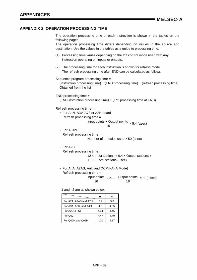
APPENDICES
APP − 39
MELSEC-A
APPENDIX 2 OPERATION PROCESSING TIMEThe operation processing time of each instruction is shown in the tables on thefollowing pages.The operation processing time differs depending on values in the source anddestination. Use the values in the tables as a guide to processing time.
(1) Processing time varies depending on the I/O control mode used with anyinstruction operating on inputs or ontputs.
(2) The processing time for each instruction is shown for refresh mode.The refresh processing time after END can be calculated as follows:
Sequence program processing time =(instruction processing time) + (END processing time) + (refresh processing time)Obtained from the list
END processing time =(END instruction processing time) + (T/C processing time at END)
Refresh processing time =• For AnN, A3V, A73 or A3N board
Refresh processing time =Input points + Output points
16• For A0J2H
Refresh processing time =Number of modules used × 50 (µsec)
• For A2CRefresh processing time =
12 × Input stations + 9.4 × Output stations +11.6 × Total stations (µsec)
• For AnA, A2AS, AnU and QCPU-A (A Mode)Refresh processing time =
Input points Output points16 16
n1 and n2 are as shown below.
n1 n2
For A2A, A2AS and A2U 5.2 5.0
For A3A, A3U, and A4U 4.8 4.65
For A2USH-S1 4.54 4.45
For Q02 4.47 4.40
For Q02H and Q06H 4.20 4.17
× 5.4 (µsec)
× n1 + × n2 (µ sec)
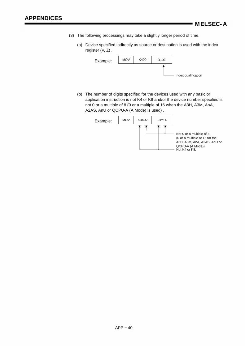
APPENDICES
APP − 40
MELSEC-A
(3) The following processings may take a slightly longer period of time.
(a) Device specified indirectly as source or destination is used with the indexregister (V, Z) .
Example:
(b) The number of digits specified for the devices used with any basic orapplication instruction is not K4 or K8 and/or the device number specified isnot 0 or a multiple of 8 (0 or a multiple of 16 when the A3H, A3M, AnA,A2AS, AnU or QCPU-A (A Mode) is used) .
Example:
MOV K400 D10Z
Index qualification
MOV K3X02 K3Y14
Not 0 or a multiple of 8(0 or a multiple of 16 for theA3H, A3M, AnA, A2AS, AnU orQCPU-A (A Mode))Not K4 or K8.•
•

APPENDICES
APP − 41
MELSEC-A
2.1 Instruction Processing Time of Small Size, Compact CPUs
(1) Sequence instructions
Table 2.1 Instruction Processing Time of Small Size, Compact CPUs
Processing Time (µµµµs)
AnS A1SJH/A1SH A2SH (S1)Instruction Condition (Device)
R D R D R D
X 1.0 2.3 0.33 2.1 0.25 1.9LD, LDI,AND, ANI,OR, ORI Y, M, L, B, F, T, C 1.0 1.0 0.33 0.33 0.25 0.25
ANBORB 1.0 1.0 0.33 0.33 0.25 0.25
Unchanged(OFF → OFF, ON → ON) 1.0 2.3 0.33 2.2 0.25 1.9
YChanged (OFF → ON, ON → OFF) 1.0 2.3 0.33 2.2 0.25 1.9
Unchanged(OFF → OFF, ON → ON) 1.0 1.0 0.33 0.33 0.25 0.25L, S, B
M (other thanspecial M) Changed (OFF → ON, ON → OFF) 1.0 1.0 0.33 0.33 0.25 0.25
Special M 37 37 9.6 9.5 7.2 7.2
Unexecuted 62 61 16.5 16.7 12.3 12.3F
Executed 270 267 69.5 84.4 52.2 52.2
Instruction execution time 1.0 1.0 0.33 0.33 0.25 0.25
Unexecuted 0 0 0 0 0 0
After time out 11 11 7.2 9.6 20.0 18.0
K 24 24 12.0 12.8 22.0 22.0
TProcessingtime at theexecutionof ENDinstruction
Exe-cuted Added
D 30 30 21.6 24.0 24.0 23.6
Instruction execution time 1.0 1.0 0.33 0.33 0.25 0.25
Unexecuted 0 0 0 0 0 0
Uncounted 0 0 0 0 0 0
After count out 0 0 0 0 0 0
K 25 25 0.8 0.8 12.0 12.8
OUT
CProcessingtime at theexecutionof ENDinstruction
Exe-ciuted
CountedD 30 30 7.2 10.4 15.2 12.0
Unexecuted 1.0 2.3 0.33 2.1 0.25 1.9
Unchanged (ON → ON) 1.0 2.3 0.33 2.1 0.25 1.9YExecuted
Changed (OFF → ON) 1.0 2.3 0.33 2.1 0.25 1.9
Unexecuted 1.0 1.0 0.33 0.33 0.25 0.25
Unchanged (ON → ON) 1.0 1.0 0.33 0.33 0.25 0.25M, L, S, BExecuted
Changed (OFF → ON) 1.0 1.0 0.33 0.33 0.25 0.25
Unexecuted 3.0 3.0 0.9 1.0 1.0 1.0Special MB Executed 32.0 32.0 7.9 8.3 6.2 6.2
Unexecuted 2.7 3.2 0.9 1.4 1.0 1.0
SET
FExecuted 232 237 62.0 61.5 46.1 46.1
R: Refresh mode, D: Direct mode
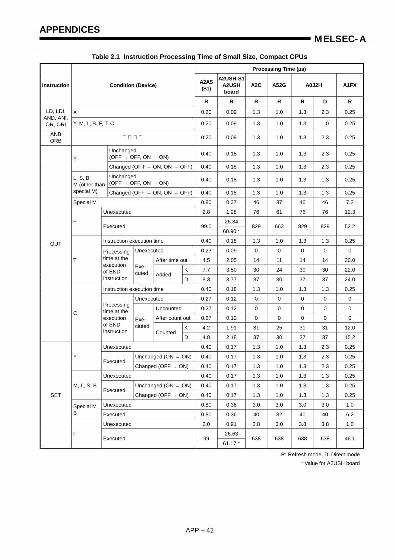
APPENDICES
APP − 42
MELSEC-A
Table 2.1 Instruction Processing Time of Small Size, Compact CPUs
Processing Time (µµµµs)
A2AS(S1)
A2USH-S1A2USHboard
A2C A52G A0J2H A1FXInstruction Condition (Device)
R R R R R D R
X 0.20 0.09 1.3 1.0 1.3 2.3 0.25LD, LDI,AND, ANI,OR, ORI Y, M, L, B, F, T, C 0.20 0.09 1.3 1.0 1.3 1.0 0.25
ANBORB 0.20 0.09 1.3 1.0 1.3 2.3 0.25
Unchanged(OFF → OFF, ON → ON) 0.40 0.18 1.3 1.0 1.3 2.3 0.25
YChanged (OF F→ ON, ON → OFF) 0.40 0.18 1.3 1.0 1.3 2.3 0.25
Unchanged(OFF → OFF, ON → ON) 0.40 0.18 1.3 1.0 1.3 1.3 0.25L, S, B
M (other thanspecial M) Changed (OFF → ON, ON → OFF) 0.40 0.18 1.3 1.0 1.3 1.3 0.25
Special M 0.80 0.37 46 37 46 46 7.2
Unexecuted 2.8 1.28 76 61 76 76 12.3
26.34FExecuted 99.0
60.90 *829 663 829 829 52.2
Instruction execution time 0.40 0.18 1.3 1.0 1.3 1.3 0.25
Unexecuted 0.23 0.09 0 0 0 0 0
After time out 4.5 2.05 14 11 14 14 20.0
K 7.7 3.50 30 24 30 30 22.0
TProcessingtime at theexecutionof ENDinstruction
Exe-cuted Added
D 8.3 3.77 37 30 37 37 24.0
Instruction execution time 0.40 0.18 1.3 1.0 1.3 1.3 0.25
Unexecuted 0.27 0.12 0 0 0 0 0
Uncounted 0.27 0.12 0 0 0 0 0
After count out 0.27 0.12 0 0 0 0 0
K 4.2 1.91 31 25 31 31 12.0
OUT
CProcessingtime at theexecutionof ENDinstruction
Exe-ciuted
CountedD 4.8 2.18 37 30 37 37 15.2
Unexecuted 0.40 0.17 1.3 1.0 1.3 2.3 0.25
Unchanged (ON → ON) 0.40 0.17 1.3 1.0 1.3 2.3 0.25YExecuted
Changed (OFF → ON) 0.40 0.17 1.3 1.0 1.3 2.3 0.25
Unexecuted 0.40 0.17 1.3 1.0 1.3 1.3 0.25
Unchanged (ON → ON) 0.40 0.17 1.3 1.0 1.3 1.3 0.25M, L, S, BExecuted
Changed (OFF → ON) 0.40 0.17 1.3 1.0 1.3 1.3 0.25
Unexecuted 0.80 0.36 3.0 3.0 3.0 3.0 1.0Special MB Executed 0.80 0.36 40 32 40 40 6.2
Unexecuted 2.0 0.91 3.8 3.0 3.8 3.8 1.0
26.63
SET
FExecuted 99
61.17 *638 638 638 638 46.1
R: Refresh mode, D: Direct mode* Value for A2USH board

APPENDICES
APP − 43
MELSEC-A
Table 2.1 Instruction Processing Time of Small Size, Compact CPUs
Processing Time (µµµµs)
AnS A1SJH/A1SH A2SH (S1)Instruction Condition (Device)
R D R D R D
Unexecuted 1.0 2.3 0.33 2.0 0.32 1.9
Unchanged(OFF → OFF) 1.0 2.3 0.33 2.0 0.32 1.9Y
ExecutedChanged (ON → OFF) 1.0 2.3 0.33 2.0 0.32 1.9
Unexecuted 1.0 1.0 0.33 0.33 0.32 0.25
Unchanged(OFF → OFF) 1.0 1.0 0.33 0.33 0.32 0.25M, L, S, B
ExecutedChanged (ON → OFF) 1.0 1.0 0.33 0.33 0.32 0.25
Unexecuted 3.0 3.0 1.4 1.4 1.0 1.0Special MB Executed 32 32 8.4 8.4 6.2 6.2
Unexecuted 3.6 3.0 1.4 1.4 1.0 1.0
OFF→OFF8.5
OFF→OFF8.4F
Executed 296 283 73.2 75.3 ON→OFF57.1
ON→OFF57.1
Unexecuted 3.0 3.0 1.4 1.4 1.0 1.0
OFF→OFF8.3
OFF→OFF8.3T, C
Executed 43 43 11.0 11.0 ON→OFF9.0
ON→OFF9.0
Unexecuted 3.0 3.0 1.4 1.4 1.0 1.0D, WA0, A1V, Z Executed 28 28 7.0 7.0 5.2 5.3
Unexecuted 3.0 3.0 1.4 1.6 1.0 1.0
RST
RExecuted 35 35 36.4 36.2 6.7 6.7
NOP 1.0 1.0 0.33 0.33 0.25 0.25
M9084 OFF 2150 2150 663.2 628.0 466.6 451.7FENDEND
M9084 ON 2060 2060 636.0 602.4 451.3 436.1
Unexecuted 43 44 15.0 13.0 8.8 10.5Y
Executed 39 41 14.0 11.9 8.0 9.7
Unexecuted 43 43 13.4 11.4 8.8 8.5MC
M, LB, F Executed 39 39 12.2 10.3 8.0 7.7
MCR 26 26 5.4 7.3 5.2 6.8
R: Refresh mode, D: Direct mode

APPENDICES
APP − 44
MELSEC-A
Table 2.1 Instruction Processing Time of Small Size, Compact CPUs
Processing Time (µµµµs)
A2AS(S1)
A2USH-S1A2USHboard
A2C A52G A0J2H A1FXInstruction Condition (Device)
R R R R R D R
Unexecuted 0.40 0.17 1.3 1.0 1.3 2.3 0.32
Unchanged(OFF → OFF) 0.40 0.17 1.3 1.0 1.3 2.3 0.32Y
ExecutedChanged (ON → OFF) 0.40 0.17 1.3 1.0 1.3 2.3 0.32
Unexecuted 0.40 0.17 1.3 1.0 1.3 1.3 0.32
Unchanged(OFF → OFF) 0.40 0.17 1.3 1.0 1.3 1.3 0.32M, L, S, B
ExecutedChanged (ON → OFF) 0.40 0.17 1.3 1.0 1.3 1.3 0.32
Unexecuted 0.80 0.36 3.0 3.0 3.0 3.0 1.0Special M
B Executed 0.80 0.36 40 32 40 40 6.2
Unexecuted 2.0 0.91 3.0 3.0 3.0 3.0 1.0
39.66 OFF→OFF8.5F
Executed 15067.09 *
596 447 596 596 ON→OFF57.1
Unexecuted 1.4 0.64 3.0 3.0 3.0 3.0 1.0
OFF→OFF8.3T, C
Executed 5.6 2.55 54 43 54 54ON→OFF
9.0
Unexecuted 1.4 0.64 3.0 3.0 3.0 3.0 1.0
V, Z
3.91D, MA0, A1V, Z Executed 8.4 Other
than V, Z
1.12
34 28 34 34 5.2
Unexecuted 1.4 0.64 3.0 3.0 3.0 3.0 1.0
RST
RExecuted 4.6 2.27 43 35 43 43 6.7
NOP 0.20 0.09 1.3 1.0 1.3 1.3 0.25
Y0 ON466.6
M9084 OFF 435 342 2688 2150 2688 2688OFF432.6
Y0 ON451.3
FENDEND
M9084 ON 285 264 2575 2060 2575 2575OFF415.3
Unexecuted 1.2 0.54 54 43 54 56 8.8Y
Executed 1.2 0.54 39 39 39 51 8.0
Unexecuted 1.2 0.54 43 43 43 54 8.8MC
M, L, B, FExecuted 1.2 0.54 39 39 39 49 8.0
MCR 0.60 0.27 26 26 26 33 5.2
R: Refresh mode, D: Direct mode* Value for A2USH board

APPENDICES
APP − 45
MELSEC-A
Table 2.1 Instruction Processing Time of Small Size, Compact CPUs
Processing Time (µµµµs)
AnS A1SJH/A1SH A2SH (S1)Instruction Condition (Device)
R D R D R D
Unexecuted 59 61 16.8 16.8 11.7 13.7
ON 62 63 17.2 17.2 11.6 13.7YExecuted
OFF 60 62 17.2 17.2 11.7 13.7
Unexecuted 59 59 15.2 15.2 11.7 11.7
ON 62 62 15.6 15.6 11.6 11.6
PLSPLF
M, L, B, FExecuted
OFF 61 61 15.6 15.6 11.7 11.6
Unexecuted 3.0 3.0 1.4 1.4 1.0 1.0Y
Executed 38 39 12.4 12.4 8.1 10.1
Unexecuted 3.0 3.0 1.4 1.4 1.0 1.0SET
SFTPM, L, B, F
Executed 38 38 10.8 10.8 8.1 8.1
MPS 1.0 1.0 0.33 0.33 0.25 0.25
MRD 1.0 1.0 0.33 0.33 0.25 0.25
MPP 1.0 1.0 0.33 0.33 0.25 0.25
Without index qualification 39 39 10.2 10.2 7.6 10.0CJ
With index qualification 48 48 12.6 12.6 9.5 11.9
Without index qualification 71 71 17.8 17.7 13.3 13.3SCJ
With index qualification 81 81 20.2 20.5 15.1 15.1
JMP 39 39 10.2 10.3 7.6 7.6
Without index qualification 74 74 17.8 17.9 13.3 13.3CALL
With index qualification 78 78 20.2 20.3 15.1 15.1
Without index qualification 70 70 17.8 17.9 13.2 13.2CALLP
With index qualification 78 78 20.2 20.3 15.1 15.1
RET 50 50 10.4 10.3 9.3 9.6
EI 38 38 9.6 9.2 7.1 7.1
DI 66 66 6.8 7.0 6.5 6.5
IRET 120 120 58.4 57.6 43.2 45.1
Without index qualification 79 79 39.8 17.6 19.0 13.0SUB
With index qualification 85 85 41.4 19.2 20.0 15.0
Without index qualification 79 79 39.8 17.6 19.0 13.0SUBP
With index qualification 85 85 41.4 19.2 20.0 15.0
M9084 OFF 2420 2420 CHG
M9084 ON 2340 2340
FOR 53 53 11.4 11.6 10.1 10.1
NEXT 41 41 8.0 8.1 7.5 8.2
STOP
R: Refresh mode, D: Direct mode

APPENDICES
APP − 46
MELSEC-A
Table 2.1 Instruction Processing Time of Small Size, Compact CPUs
Processing Time (µµµµs)
A2AS(S1)
A2USH-S1A2USHboard
A2C A52G A0J2H A1FXInstruction Condition (Device)
R R R R R D R
Unexecuted 2.2 0.99 59 59 59 76 11.7
ON 2.2 0.99 62 62 62 79 11.6YExecuted
OFF 2.2 0.99 60 60 60 77 11.7
Unexecuted 2.2 0.99 59 59 59 74 11.7
ON 2.2 0.99 62 62 62 78 11.6
PLSPLF
M, L, B, FExecuted
OFF 2.2 0.99 61 61 61 76 11.7
Unexecuted 1.4 0.63 3.0 3.0 3.0 3.0 1.0Y
Executed 4.4 1.99 47 38 47 49 8.1
Unexecuted 1.4 0.63 3.0 3.0 3.0 3.0 1.0SET
SFTPM, L, B, F
Executed 4.4 1.99 47 38 47 47 8.1
MPS 0.20 0.09 1.3 1.0 1.3 1.3 0.25
MRD 0.20 0.09 1.3 1.0 1.3 1.3 0.25
MPP 0.20 0.09 1.3 1.0 1.3 1.3 0.25
Without index qualification 6.6 3.08 49 39 49 49 10.0CJ
With index qualification 6.6 3.08 60 48 60 60 11.9
Without index qualification 6.6 3.08 89 71 89 89 13.3SCJ
With index qualification 6.6 3.08 101 81 101 101 15.1
JMP 6.6 3.08 49 39 49 49 7.6
Without index qualification 10 4.82 93 74 93 93 13.3CALL
With index qualification 10 4.82 98 78 98 98 15.1
Without index qualification 10 4.82 87 70 87 87 13.2CALLP
With index qualification 10 4.82 98 78 98 98 15.1
RET 7.0 3.19 63 50 63 63 9.3
EI 3.0 1.08 47 38 47 47 7.1
DI 3.2 1.08 82 66 82 82 6.5
IRET 3.4 1.08 150 120 150 150 43.2
Without index qualification 98 79 98 98 19.0SUB
With index qualification 107 85 107 107 20.0
Without index qualification 98 79 98 98 19.0SUBP
With index qualification 107 85 107 107 20.0
M9084 OFF 450 3025 2420 3025 3025 CHG
M9084 ON 301 2925 2340 2925 2925
FOR 5.8 2.73 67 53 67 67 10.1
NEXT 8.0 3.47 51 41 51 51 7.5
STOP
R: Refresh mode, D: Direct mode

APPENDICES
APP − 47
MELSEC-A
POINTS
(1) "When not executed" in the above table indicates that the input conditionis off.
(2) "When not counted" of OUT C instruction indicates that the input conditionremains on and the counter does not count.
(3) "OFF" of PLS and PLF instructions indicates that the input conditionremains on 1 scan after it has turned on (off for PLF), and the pulse is notgenerated.
(4) T/C count processing time and refresh time are not included in the FEND,END, CHG instruction processing times.
Input condition
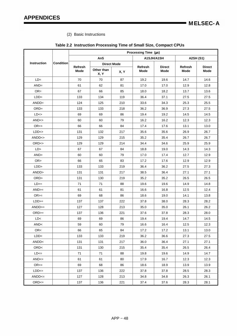
APPENDICES
APP − 48
MELSEC-A
(2) Basic Instructions
Table 2.2 Instruction Processing Time of Small Size, Compact CPUs
Processing Time (µµµµs)
AnS A1SJH/A1SH A2SH (S1)
Direct ModeInstruction ConditionRefreshMode Other than
X, Y X, YRefreshMode
DirectMode
RefreshMode
DirectMode
LD= 70 70 87 19.2 19.6 14.7 14.6
AND= 61 62 81 17.0 17.0 12.9 12.8
OR= 67 66 85 18.0 18.2 13.7 13.6
LDD= 133 134 119 36.4 37.1 27.5 27.5
ANDD= 124 125 210 33.6 34.3 25.3 25.5
ORD= 133 133 218 36.2 36.9 27.3 27.5
LD<> 69 69 86 19.4 19.2 14.5 14.5
AND<> 60 60 79 16.2 16.2 12.3 12.3
OR<> 66 66 84 17.4 17.6 13.1 13.0
LDD<> 131 132 217 35.6 35.6 26.9 26.7
ANDD<> 129 129 215 35.2 35.4 26.7 26.7
ORD<> 129 129 214 34.4 34.6 25.9 25.9
LD> 67 67 84 18.8 19.0 14.3 14.3
AND> 60 60 79 17.0 17.4 12.7 12.9
OR> 66 65 83 17.2 17.6 12.9 12.9
LDD> 133 133 219 36.4 36.2 27.5 27.3
ANDD> 131 131 217 38.5 36.4 27.1 27.1
ORD> 131 130 219 35.2 35.2 26.5 26.5
LD>= 71 71 88 19.6 19.6 14.9 14.8
AND>= 61 61 81 16.6 16.8 12.5 12.4
OR>= 69 68 86 18.6 19.0 14.1 13.8
LDD>= 137 137 222 37.8 38.0 28.3 28.2
ANDD>= 127 128 213 35.0 35.0 26.1 26.2
ORD>= 137 136 221 37.6 37.8 28.3 28.0
LD< 69 69 86 19.4 19.4 14.7 14.5
AND< 59 60 79 16.6 16.4 12.5 12.3
OR< 66 65 84 17.2 17.2 13.1 13.0
LDD< 133 133 219 36.2 36.6 27.3 27.5
ANDD< 131 131 217 36.0 36.4 27.1 27.1
ORD< 131 130 215 35.4 35.4 26.5 26.4
LD<= 71 71 88 19.8 19.6 14.9 14.7
AND<= 61 61 80 17.9 16.7 12.3 12.3
OR<= 69 68 86 18.6 18.9 13.9 13.9
LDD<= 137 136 222 37.8 37.8 28.5 28.3
ANDD<= 127 128 213 34.8 34.8 26.3 26.1
ORD<= 137 136 221 37.4 37.6 28.3 28.1

APPENDICES
APP − 49
MELSEC-A
Table 2.2 Instruction Processing Time of Small Size, Compact CPUsProcessing Time (µµµµs)
A2AS (S1)A2USH-S1
A2USHboard
A2C A52G A0J2H A1FX
Direct ModeInstruction Condition
RefreshMode
RefreshMode
RefreshMode
RefreshMode
RefreshMode Other
than X, Y X, YRefreshMode
LD= 3.8 1.91 88 70 88 88 109 14.7AND= 2.6 1.45 76 61 76 77 101 12.9OR= 2.8 2.00 84 67 84 83 106 13.7LDD= 10 5.18 166 133 166 168 149 27.5
ANDD= 5.9 4.64 155 124 155 156 263 25.31.99
ORD= 6.34.53 *
166 133 166 167 273 27.3
LD<> 4.1 1.91 86 69 86 87 108 14.5AND<> 2.6 1.45 75 60 75 75 99 12.3OR<> 2.8 2.00 83 66 83 82 105 13.1LDD<> 10 5.18 164 131 164 166 272 26.9
ANDD<> 5.9 4.64 161 129 161 162 269 26.71.99
ORD<> 6.14.53 *
161 129 161 161 268 25.9
LD> 4.1 1.91 84 67 84 84 106 14.3AND> 2.6 1.45 75 60 75 75 99 12.7OR> 2.8 2.00 83 66 83 81 104 12.9LDD> 9.7 5.18 166 133 166 167 274 27.5
ANDD> 5.8 4.64 164 131 164 164 272 27.11.99
ORD> 6.04.53 *
164 131 164 163 274 26.5
LD>= 4.1 1.91 88 71 88 89 110 14.9AND>= 2.6 1.45 76 66 76 77 101 12.5OR>= 2.8 2.00 86 69 86 86 108 14.1LDD>= 9.7 5.18 171 137 171 172 278 28.3
ANDD>= 5.8 4.64 159 127 159 161 267 26.11.99
ORD>= 6.04.53 *
171 137 171 171 277 28.3
LD< 4.1 1.91 86 69 86 87 108 14.7AND< 2.6 1.45 74 59 74 75 99 12.5OR< 2.8 2.00 83 66 83 82 105 13.1LDD< 9.7 5.18 166 133 166 167 274 27.3
ANDD< 5.8 4.64 164 131 164 164 272 27.11.99
ORD< 6.04.53 *
164 131 164 163 269 26.5
LD<= 4.1 1.91 89 71 89 89 110 14.9AND<= 2.6 1.45 76 61 76 77 101 12.3OR<= 2.8 2.00 86 69 86 85 108 13.9LDD<= 9.7 5.18 171 137 171 171 278 28.5
ANDD<= 5.8 4.64 160 127 160 161 267 26.31.99
ORD<= 6.04.53 *
171 137 171 171 277 28.3
* Value for A2USH board

APPENDICES
APP − 50
MELSEC-A
Table 2.2 Instruction Processing Time of Small Size, Compact CPUs
Processing Time (µµµµs)
AnS A1SJH/A1SH A2SH (S1)
Direct ModeInstruction ConditionRefreshMode Other than
X, Y X, YRefreshMode
DirectMode
RefreshMode
DirectMode
+ S D 44 45 59 11.6 11.9 8.7 8.6
+P S D 44 45 59 11.4 12.1 8.6 8.6
D+ S D 69 69 90 18.2 18.5 13.7 13.6
D+P S D 69 69 90 18.0 18.3 13.6 13.2
+ S1 S2 D 77 77 103 20.2 20.7 15.3 15.2
+P S1 S2 D 77 77 103 20.2 20.5 15.2 14.8
D+ S1 S2 D 99 99 246 25.6 25.9 19.3 19.2
D+P S1 S2 D 99 99 246 25.8 26.3 19.4 19.2
- S D 45 45 59 11.6 12.1 8.7 8.6
-P S D 45 45 59 11.8 12.1 8.6 8.6
D- S D 69 69 90 18.0 18.5 13.7 13.6
D-P S D 69 69 90 18.0 18.7 13.6 13.2
- S1 S2 D 79 79 107 20.8 21.3 15.7 15.6
-P S1 S2 D 79 79 107 20.8 21.3 15.8 15.6
D- S1 S2 D 99 99 130 27.0 25.7 20.3 20.4
D-P S1 S2 D 99 99 130 26.8 27.3 20.4 20.2
∗ S1 S2 D 94 95 168 22.0 22.7 16.5 16.4
∗ P S1 S2 D 94 95 168 21.8 22.7 16.6 16.6
D∗ S1 S2 D 341 340 370 98.2 98.3 73.7 73.6
D∗ P S1 S2 D 341 340 370 98.2 98.5 73.6 73.8
/ S1 S2 D 102 103 99 23.2 23.9 17.7 17.4
/P S1 S2 D 102 103 99 23.2 23.9 17.4 17.4
D/ S1 S2 D 393 394 412 106.8 107.5 80.1 80.2
D/P S1 S2 D 393 394 412 106.6 107.3 80.2 80.2
INC 29 29 38 7.2 7.5 5.7 5.4
INCP 29 29 38 7.4 7.7 5.4 5.4
DINC 42 42 132 10.6 11.3 8.1 8.0
DINCP 42 42 132 10.6 11.1 7.9 7.8
DEC 31 31 39 7.8 8.5 6.1 5.8
DECP 31 31 39 7.8 8.3 5.9 5.8
DDEC 42 42 54 10.6 11.1 8.1 8.0
DDECP 42 42 54 2.7 1.9 8.1 7.8

APPENDICES
APP − 51
MELSEC-A
Table 2.2 Instruction Processing Time of Small Size, Compact CPUs
Processing Time (µµµµs)
A2AS (S1)A2USH-S1
A2USHboard
A2C A52G A0J2H A1FX
Direct ModeInstruction Condition
RefreshMode
RefreshMode
RefreshMode
RefreshMode
RefreshMode Other
than X, Y X, YRefreshMode
+ S D 2.8 1.28 55 44 55 56 74 8.7
+P S D 2.8 1.28 55 44 55 56 74 8.6
D+ S D 4.0 1.82 86 69 86 87 113 13.7
D+P S D 4.0 1.82 86 69 86 87 113 13.6
+ S1 S2 D 3.2 1.45 96 77 96 97 129 15.3
+P S1 S2 D 3.2 1.45 96 77 96 97 129 15.2
D+ S1 S2 D 4.6 2.09 124 99 124 124 308 19.3
D+P S1 S2 D 4.6 2.09 124 99 124 124 308 19.4
- S D 2.8 1.27 56 45 56 57 74 8.7
-P S D 2.8 1.27 56 45 56 57 74 8.6
D- S D 4.0 1.82 86 69 86 87 113 13.7
D-P S D 4.0 1.82 86 69 86 87 113 13.6
- S1 S2 D 3.2 1.45 99 79 99 99 134 15.7
-P S1 S2 D 3.2 1.45 99 79 99 99 134 15.8
D- S1 S2 D 4.6 2.09 124 99 124 124 163 20.3
D-P S1 S2 D 4.6 2.09 124 99 124 124 163 20.4
∗ S1 S2 D 3.4 1.55 118 94 118 119 211 16.5
∗ P S1 S2 D 3.4 1.55 118 94 118 119 211 16.6
D∗ S1 S2 D 20 7.45 426 341 426 426 463 73.7
D∗ P S1 S2 D 20 7.45 426 341 426 426 463 73.6
/ S1 S2 D 11 5.18 128 102 128 129 124 17.7
/P S1 S2 D 11 5.18 128 102 128 129 124 17.4
D/ S1 S2 D 36 15.72 491 393 491 493 516 80.1
D/P S1 S2 D 36 15.72 491 393 491 493 516 80.2
INC 2.0 0.91 36 29 36 37 47 5.7
INCP 2.0 0.91 36 29 36 37 47 5.4
DINC 2.4 1.09 53 42 53 53 166 8.1
DINCP 2.4 1.09 53 42 53 53 166 7.9
DEC 2.0 0.91 39 31 39 39 49 6.1
DECP 2.0 0.91 39 31 39 39 49 5.9
DDEC 2.4 1.09 53 42 53 53 67 8.1
DDECP 2.4 1.09 53 42 53 53 67 8.1

APPENDICES
APP − 52
MELSEC-A
Table 2.2 Instruction Processing Time of Small Size, Compact CPUs
Processing Time (µµµµs)
AnS A1SJH/A1SH A2SH (S1)
Direct ModeInstruction ConditionRefreshMode Other than
X, Y X, YRefreshMode
DirectMode
RefreshMode
DirectMode
B+ S D 123 123 183 33.6 34.1 25.3 25.2
B+P S D 123 123 183 34.0 34.3 25.2 25.0
DB+ S D 175 176 280 47.0 47.5 35.2 35.2
DB+P S D 175 176 280 46.8 47.7 35.4 35.0
B+ S1 S2 D 129 129 192 35.2 35.7 26.5 26.4
B+P S1 S2 D 129 129 192 35.2 35.5 26.6 26.2
DB+ S1 S2 D 187 186 294 50.2 50.9 37.7 37.8
DB+P S1 S2 D 187 186 294 50.2 50.5 37.5 37.8
B- S D 125 125 185 33.2 33.7 24.9 24.8
B-P S D 125 125 185 33.0 33.7 24.9 24.6
DB- S D 175 175 280 46.8 47.3 35.3 35.0
DB-P S D 175 175 280 46.8 47.3 35.1 35.0
B- S1 S2 D 133 133 203 36.2 36.9 27.3 27.0
B-P S1 S2 D 133 133 203 36.2 36.7 27.1 27.0
DB- S1 S2 D 185 186 294 50.4 50.6 38.1 37.8
DB-P S1 S2 D 185 186 294 50.4 51.1 37.9 37.4
B∗ S1 S2 D 299 300 358 79.8 80.1 60.1 59.4
B∗ P S1 S2 D 299 300 358 80.0 80.1 59.7 59.8
DB∗ S1 S2 D 941 939 1044 245.6 246.3 184.3 184.2
DB∗ P S1 S2 D 941 939 1044 245.8 246.1 184.3 184.2
B/ S1 S2 D 235 236 274 61.4 61.7 46.2 46.6
B/P S1 S2 D 235 236 274 61.2 61.7 46.1 46.6
DB/ S1 S2 D 896 894 954 246.4 246.9 185.1 184.8
DB/P S1 S2 D 896 894 954 246.0 276.5 184.5 184.8
BCD 82 83 90 22.0 22.3 16.3 16.5
BCDP 82 83 90 22.0 22.5 16.7 16.6
DBCD 219 220 284 59.2 59.7 44.3 44.4
DBCDP 219 220 284 59.2 59.7 44.5 44.8
BIN 79 78 86 20.8 21.5 15.7 16.0
BINP 79 78 86 20.8 21.3 15.7 15.8
DBIN 215 216 280 58.2 58.9 43.9 43.8
DBINP 215 216 280 58.2 58.9 43.7 43.8
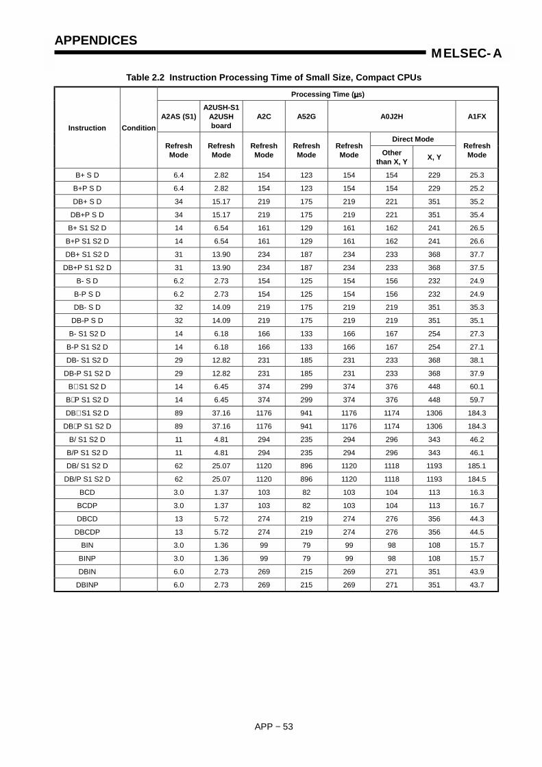
APPENDICES
APP − 53
MELSEC-A
Table 2.2 Instruction Processing Time of Small Size, Compact CPUs
Processing Time (µµµµs)
A2AS (S1)A2USH-S1
A2USHboard
A2C A52G A0J2H A1FX
Direct ModeInstruction Condition
RefreshMode
RefreshMode
RefreshMode
RefreshMode
RefreshMode Other
than X, Y X, YRefreshMode
B+ S D 6.4 2.82 154 123 154 154 229 25.3
B+P S D 6.4 2.82 154 123 154 154 229 25.2
DB+ S D 34 15.17 219 175 219 221 351 35.2
DB+P S D 34 15.17 219 175 219 221 351 35.4
B+ S1 S2 D 14 6.54 161 129 161 162 241 26.5
B+P S1 S2 D 14 6.54 161 129 161 162 241 26.6
DB+ S1 S2 D 31 13.90 234 187 234 233 368 37.7
DB+P S1 S2 D 31 13.90 234 187 234 233 368 37.5
B- S D 6.2 2.73 154 125 154 156 232 24.9
B-P S D 6.2 2.73 154 125 154 156 232 24.9
DB- S D 32 14.09 219 175 219 219 351 35.3
DB-P S D 32 14.09 219 175 219 219 351 35.1
B- S1 S2 D 14 6.18 166 133 166 167 254 27.3
B-P S1 S2 D 14 6.18 166 133 166 167 254 27.1
DB- S1 S2 D 29 12.82 231 185 231 233 368 38.1
DB-P S1 S2 D 29 12.82 231 185 231 233 368 37.9
B∗ S1 S2 D 14 6.45 374 299 374 376 448 60.1
B∗ P S1 S2 D 14 6.45 374 299 374 376 448 59.7
DB∗ S1 S2 D 89 37.16 1176 941 1176 1174 1306 184.3
DB∗ P S1 S2 D 89 37.16 1176 941 1176 1174 1306 184.3
B/ S1 S2 D 11 4.81 294 235 294 296 343 46.2
B/P S1 S2 D 11 4.81 294 235 294 296 343 46.1
DB/ S1 S2 D 62 25.07 1120 896 1120 1118 1193 185.1
DB/P S1 S2 D 62 25.07 1120 896 1120 1118 1193 184.5
BCD 3.0 1.37 103 82 103 104 113 16.3
BCDP 3.0 1.37 103 82 103 104 113 16.7
DBCD 13 5.72 274 219 274 276 356 44.3
DBCDP 13 5.72 274 219 274 276 356 44.5
BIN 3.0 1.36 99 79 99 98 108 15.7
BINP 3.0 1.36 99 79 99 98 108 15.7
DBIN 6.0 2.73 269 215 269 271 351 43.9
DBINP 6.0 2.73 269 215 269 271 351 43.7

APPENDICES
APP − 54
MELSEC-A
Table 2.2 Instruction Processing Time of Small Size, Compact CPUs
Processing Time (µµµµs)
AnS A1SJH/A1SH A2SH (S1)
Direct ModeInstruction ConditionRefreshMode Other than
X, Y X, YRefreshMode
DirectMode
RefreshMode
DirectMode
MOV 47 47 57 11.8 12.3 9.1 9.0
MOVP 47 47 57 11.8 12.5 8.9 9.0
DMOV 67 67 87 17.2 17.7 13.1 13.0
DMOVP 67 67 87 17.2 17.9 13.1 13.0
XCH 60 61 84 15.8 16.3 11.9 11.8
XCHP 60 61 84 15.8 16.3 11.9 11.8
DXCH 107 107 141 28.8 29.5 21.7 21.6
DXCHP 107 107 141 28.8 29.1 21.7 21.8
CML 43 43 57 10.8 11.5 8.3 8.4
CMLP 43 43 57 10.8 11.5 8.3 8.2
DCML 74 75 108 20.2 20.9 15.1 15.2
DCMLP 74 75 108 20.2 20.7 15.3 15.0
BMOV S D n n=96 399 400 7144 59.2 59.5 44.4 44.4
BMOVP S D n n=96 399 400 7144 59.2 59.5 44.5 44.3
FMOV S D n n=96 229 228 1029 33.8 34.5 25.4 25.4
FMOVP S D n n=96 229 228 1029 33.8 34.3 25.5 25.4

APPENDICES
APP − 55
MELSEC-A
Table 2.2 Instruction Processing Time of Small Size, Compact CPUs
Processing Time (µµµµs)
A2AS (S1)A2USH-S1
A2USHboard
A2C A52G A0J2H A1FX
Direct ModeInstruction Condition
RefreshMode
RefreshMode
RefreshMode
RefreshMode
RefreshMode Other
than X, Y X, YRefreshMode
MOV 1.2 0.55 59 47 59 59 71 9.1
MOVP 1.2 0.55 59 47 59 59 71 8.9
DMOV 3.2 1.45 84 67 84 84 109 13.1
DMOVP 3.2 1.45 84 67 84 84 109 13.1
XCH 2.8 1.27 75 60 75 76 105 11.9
XCHP 2.8 1.27 75 60 75 76 105 11.9
DXCH 4.2 1.82 134 107 134 134 177 21.7
DXCHP 4.2 1.82 134 107 134 134 177 21.7
CML 2.4 1.09 54 43 54 54 72 8.3
CMLP 2.4 1.09 54 43 54 54 72 8.3
DCML 3.2 1.45 93 74 93 94 136 15.1
DCMLP 3.2 1.45 93 74 93 94 136 15.3
BMOV S D n n=96 72 32.73 499 399 499 501 8931 44.4
BMOVP S D n n=96 72 32.73 499 399 499 501 8931 44.5
FMOV S D n n=96 32 14.65 286 229 286 286 1287 25.4
FMOVP S D n n=96 32 14.65 286 229 286 286 1287 25.5
POINTS
(1) All the basic instructions indicated above are used without indexqualification.
(2) When unexecuted, any instruction is processed during the following time:
An, A2C and A0J2H............................... (Number of steps + 1) x 1.3 (µs)AnN, AnS, A3V,A73 and A3N board...... (Number of steps + 1) x 1.0 (µs)A1SH, A1SJH ........................................ (Number of steps + 1) x 0.33 (µs)A2SH (S1), A1FX................................... (Number of steps + 1) x 0.25 (µs)A3H and A3M......................................... (Number of steps + 1) x 0.2 (µs)A2A, A2AS and A2U.............................. (Number of steps + 4) x 0.2 (µs)A3A, A3U and A4U ................................ (Number of steps + 4) x 0.15 (µs)A2USH-S1, A2USH board ..................... (Number of steps + 7) x 0.09 (µs)
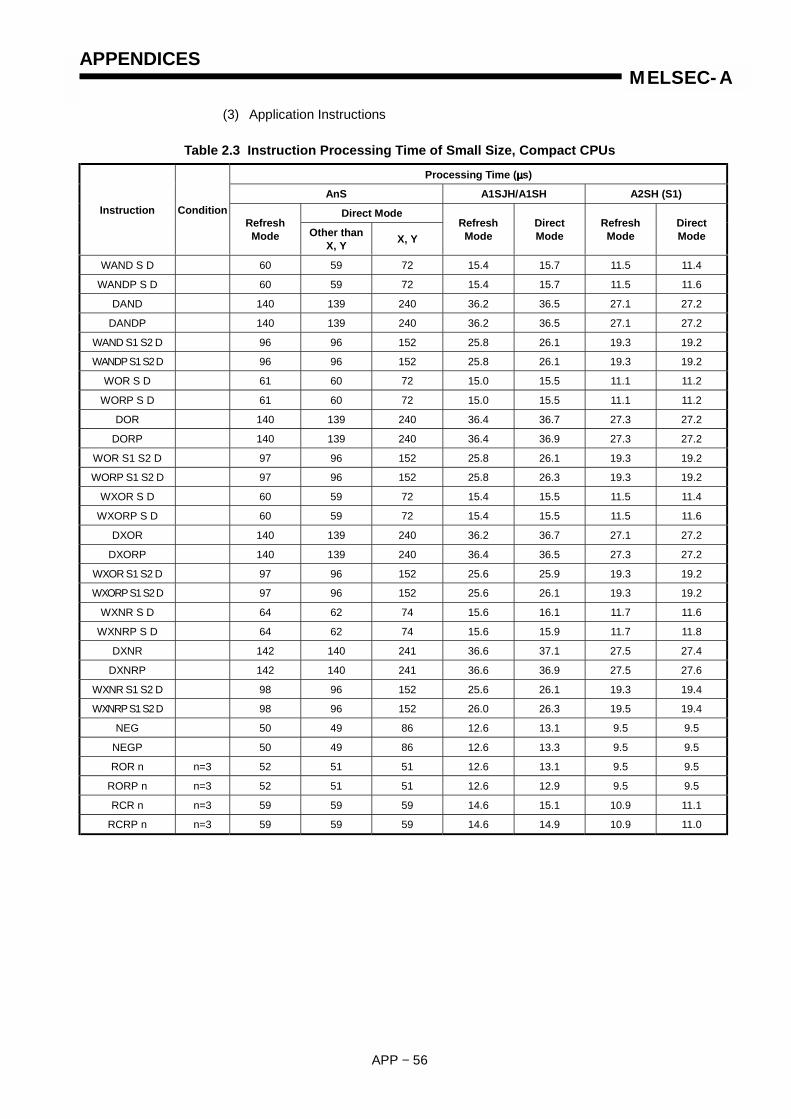
APPENDICES
APP − 56
MELSEC-A
(3) Application Instructions
Table 2.3 Instruction Processing Time of Small Size, Compact CPUs
Processing Time (µµµµs)
AnS A1SJH/A1SH A2SH (S1)
Direct ModeInstruction ConditionRefreshMode Other than
X, Y X, YRefreshMode
DirectMode
RefreshMode
DirectMode
WAND S D 60 59 72 15.4 15.7 11.5 11.4
WANDP S D 60 59 72 15.4 15.7 11.5 11.6
DAND 140 139 240 36.2 36.5 27.1 27.2
DANDP 140 139 240 36.2 36.5 27.1 27.2
WAND S1 S2 D 96 96 152 25.8 26.1 19.3 19.2
WANDP S1 S2 D 96 96 152 25.8 26.1 19.3 19.2
WOR S D 61 60 72 15.0 15.5 11.1 11.2
WORP S D 61 60 72 15.0 15.5 11.1 11.2
DOR 140 139 240 36.4 36.7 27.3 27.2
DORP 140 139 240 36.4 36.9 27.3 27.2
WOR S1 S2 D 97 96 152 25.8 26.1 19.3 19.2
WORP S1 S2 D 97 96 152 25.8 26.3 19.3 19.2
WXOR S D 60 59 72 15.4 15.5 11.5 11.4
WXORP S D 60 59 72 15.4 15.5 11.5 11.6
DXOR 140 139 240 36.2 36.7 27.1 27.2
DXORP 140 139 240 36.4 36.5 27.3 27.2
WXOR S1 S2 D 97 96 152 25.6 25.9 19.3 19.2
WXORP S1 S2 D 97 96 152 25.6 26.1 19.3 19.2
WXNR S D 64 62 74 15.6 16.1 11.7 11.6
WXNRP S D 64 62 74 15.6 15.9 11.7 11.8
DXNR 142 140 241 36.6 37.1 27.5 27.4
DXNRP 142 140 241 36.6 36.9 27.5 27.6
WXNR S1 S2 D 98 96 152 25.6 26.1 19.3 19.4
WXNRP S1 S2 D 98 96 152 26.0 26.3 19.5 19.4
NEG 50 49 86 12.6 13.1 9.5 9.5
NEGP 50 49 86 12.6 13.3 9.5 9.5
ROR n n=3 52 51 51 12.6 13.1 9.5 9.5
RORP n n=3 52 51 51 12.6 12.9 9.5 9.5
RCR n n=3 59 59 59 14.6 15.1 10.9 11.1
RCRP n n=3 59 59 59 14.6 14.9 10.9 11.0
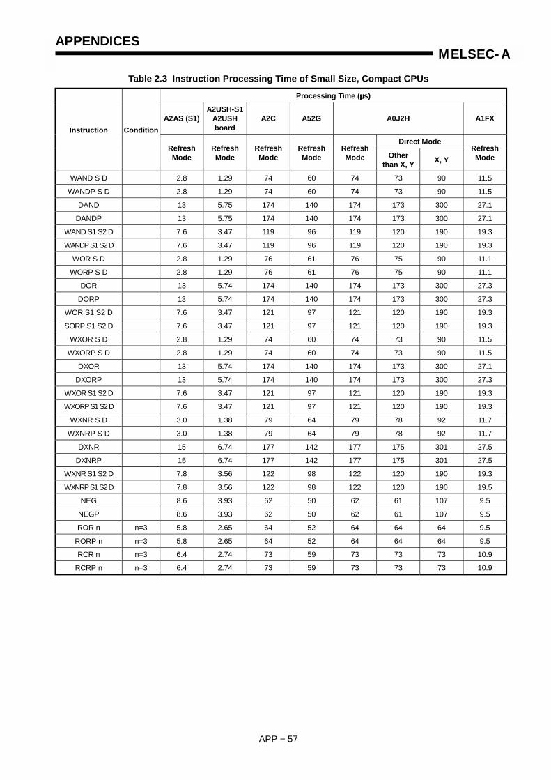
APPENDICES
APP − 57
MELSEC-A
Table 2.3 Instruction Processing Time of Small Size, Compact CPUs
Processing Time (µµµµs)
A2AS (S1)A2USH-S1
A2USHboard
A2C A52G A0J2H A1FX
Direct ModeInstruction Condition
RefreshMode
RefreshMode
RefreshMode
RefreshMode
RefreshMode Other
than X, Y X, YRefreshMode
WAND S D 2.8 1.29 74 60 74 73 90 11.5
WANDP S D 2.8 1.29 74 60 74 73 90 11.5
DAND 13 5.75 174 140 174 173 300 27.1
DANDP 13 5.75 174 140 174 173 300 27.1
WAND S1 S2 D 7.6 3.47 119 96 119 120 190 19.3
WANDP S1 S2 D 7.6 3.47 119 96 119 120 190 19.3
WOR S D 2.8 1.29 76 61 76 75 90 11.1
WORP S D 2.8 1.29 76 61 76 75 90 11.1
DOR 13 5.74 174 140 174 173 300 27.3
DORP 13 5.74 174 140 174 173 300 27.3
WOR S1 S2 D 7.6 3.47 121 97 121 120 190 19.3
SORP S1 S2 D 7.6 3.47 121 97 121 120 190 19.3
WXOR S D 2.8 1.29 74 60 74 73 90 11.5
WXORP S D 2.8 1.29 74 60 74 73 90 11.5
DXOR 13 5.74 174 140 174 173 300 27.1
DXORP 13 5.74 174 140 174 173 300 27.3
WXOR S1 S2 D 7.6 3.47 121 97 121 120 190 19.3
WXORP S1 S2 D 7.6 3.47 121 97 121 120 190 19.3
WXNR S D 3.0 1.38 79 64 79 78 92 11.7
WXNRP S D 3.0 1.38 79 64 79 78 92 11.7
DXNR 15 6.74 177 142 177 175 301 27.5
DXNRP 15 6.74 177 142 177 175 301 27.5
WXNR S1 S2 D 7.8 3.56 122 98 122 120 190 19.3
WXNRP S1 S2 D 7.8 3.56 122 98 122 120 190 19.5
NEG 8.6 3.93 62 50 62 61 107 9.5
NEGP 8.6 3.93 62 50 62 61 107 9.5
ROR n n=3 5.8 2.65 64 52 64 64 64 9.5
RORP n n=3 5.8 2.65 64 52 64 64 64 9.5
RCR n n=3 6.4 2.74 73 59 73 73 73 10.9
RCRP n n=3 6.4 2.74 73 59 73 73 73 10.9

APPENDICES
APP − 58
MELSEC-A
Table 2.3 Instruction Processing Time of Small Size, Compact CPUs
Processing Time (µµµµs)
AnS A1SJH/A1SH A2SH (S1)
Direct ModeInstruction ConditionRefreshMode Other than
X, Y X, YRefreshMode
DirectMode
RefreshMode
DirectMode
ROL n n=3 54 53 53 13.2 13.7 9.9 10.0
ROLP n n=3 54 53 53 13.4 13.7 9.9 10.1
RCL n n=3 57 57 57 15.2 15.7 11.3 11.4
RCLP n n=3 57 57 57 15.2 15.5 11.5 11.4
DROR n n=3 70 69 69 18.4 18.7 13.7 13.8
DRORP n n=3 70 69 69 18.2 18.9 13.1 13.7
DRCR n n=3 72 72 72 18.0 18.3 13.5 13.5
DRCRP n n=3 72 72 72 18.0 18.5 13.5 13.4
DROL n n=3 69 69 69 18.4 18.7 13.7 13.8
DROLP n n=3 69 69 69 18.2 18.9 13.1 13.7
DRCL n n=3 68 68 68 18.8 19.1 14.1 14.1
DRCLP n n=3 68 68 68 18.8 18.9 14.1 14.0
SFR D n n=5 74 72 83 18.4 17.5 13.7 13.8
SFRP D n n=5 74 72 83 18.4 18.9 13.7 13.8
n=5 124 123 124 31.6 31.7 23.7 23.8BSFR D n
n=15 — — — 33.6 33.9 25.1 25.2
n=5 124 123 124 31.6 31.9 23.5 23.5BSFRP D n
n=15 — — — 33.6 33.9 25.3 25.0
DSFR D n n=5 118 116 — 30.2 30.5 22.5 22.6
DSFRP D n n=5 118 116 — 30.2 30.5 22.7 22.8
SFL D n n=5 74 73 84 19.2 19.5 14.3 14.4
SFLP D n n=5 74 73 84 19.2 19.7 14.3 14.6
n=5 134 133 134 34.4 34.7 25.7 25.8BSFL D n
n=15 — — — 36.0 36.5 26.9 27.2
n=5 134 133 134 34.4 34.9 25.9 25.8BSFLP n
n=15 — — — 36.0 36.5 27.1 27.0
DSFL D n n=5 118 17 — 30.4 30.9 22.7 22.8
DSFLP D n n=5 118 17 — 30.4 30.9 22.9 22.8
SER S1 S2 n n=5 200 200 — 49.8 50.1 37.3 37.2
SERP S1 S2 n n=5 200 200 — 49.8 50.3 37.5 37.4
SUM 115 114 131 30.8 31.1 23.1 23.2
SUMP 115 114 131 30.8 31.3 23.3 23.2
DSUM 200 119 231 53.8 54.3 40.3 40.4
DSUMP 200 119 231 53.8 54.3 40.5 40.4
DECO S D n n=2 164 163 216 43.2 43.7 32.3 32.4
DECOP S D n n=2 164 163 216 43.2 43.9 32.5 32.4
SEG 91 91 155 25.7 25.7 19.8 19.7
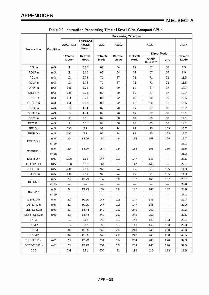
APPENDICES
APP − 59
MELSEC-A
Table 2.3 Instruction Processing Time of Small Size, Compact CPUs
Processing Time (µµµµs)
A2AS (S1)A2USH-S1
A2USHboard
A2C A52G A0J2H A1FX
Direct ModeInstruction Condition
RefreshMode
RefreshMode
RefreshMode
RefreshMode
RefreshMode Other
than X, Y X, YRefreshMode
ROL n n=3 11 2.66 67 54 67 67 67 9.9
ROLP n n=3 11 2.66 67 54 67 67 67 9.9
RCL n n=3 12 2.74 71 57 71 71 71 11.3
RCLP n n=3 12 2.74 71 57 71 71 71 11.5
DROR n n=3 5.8 5.02 87 70 87 87 87 13.7
DRORP n n=3 5.8 5.02 87 70 87 87 87 13.7
DRCR n n=3 6.4 5.38 89 72 89 90 90 13.5
DRCRP n n=3 6.4 5.38 89 72 89 90 90 13.5
DROL n n=3 10 4.74 87 70 87 87 87 13.7
DROLP n n=3 10 4.74 87 70 87 87 87 13.1
DRCL n n=3 12 5.11 84 68 84 85 85 14.1
DRCLP n n=3 12 5.11 84 68 84 85 85 14.1
SFR D n n=5 5.0 2.1 92 74 92 90 103 13.7
SFRP D n n=5 5.0 2.1 92 74 92 90 103 13.7
n=5 29 13.09 154 124 154 153 155 23.7BSFR D n
n=15 — — — — — — — 25.1
n=5 29 13.09 154 124 154 153 155 23.5BSFRP D n
n=15 — — — — — — — 25.3
DSFR D n n=5 18.8 8.55 147 118 147 145 — 22.5
DSFRP D n n=5 18.8 8.55 147 118 147 145 — 22.7
SFL D n n=5 4.8 2.19 92 74 92 91 105 14.3
SFLP D n n=5 4.8 2.19 92 74 92 91 105 14.3
n=5 28 12.73 167 134 167 166 167 25.7BSFL D n
n=15 — — — — — — — 26.9
n=5 28 12.73 167 134 167 166 167 25.9BSFLP n
n=15 — — — — — — — 27.1
DSFL D n n=5 22 10.00 147 118 147 146 — 22.7
DSFLP D n n=5 22 10.00 147 118 147 146 — 22.9
SER S1 S2 n n=5 33 14.44 249 200 249 250 — 37.3
SERP S1 S2 n n=5 33 14.44 249 200 249 250 — 37.5
SUM 15 6.82 143 115 143 143 163 23.1
SUMP 15 6.82 143 115 143 143 163 23.3
DSUM 34 15.35 249 200 249 248 288 40.3
DSUMP 34 15.35 249 200 248 249 288 40.5
DECO S D n n=2 28 12.73 204 164 204 203 270 32.3
DECOP S D n n=2 28 12.73 204 164 204 203 270 32.5
SEG 6.4 2.91 800 91 113 113 193 19.8

APPENDICES
APP − 60
MELSEC-A
Table 2.3 Instruction Processing Time of Small Size, Compact CPUs
Processing Time (µµµµs)
AnS A1SJH/A1SH A2SH (S1)
Direct ModeInstruction ConditionRefreshMode Other than
X, Y X, YRefreshMode
DirectMode
RefreshMode
DirectMode
ENCO S D n n=2 164 163 195 92.6 93.1 69.5 69.4
ENCOP S D n n=2 164 163 195 92.6 93.1 69.4 69.4
BSET D n n=5 90 90 — 23.6 23.9 17.7 18.0
BSETP D n n=5 90 90 — 23.6 24.1 17.5 18.0
BRST D n n=5 97 96 — 25.0 25.5 18.7 18.8
BRSTP D n n=5 97 96 — 25.0 25.5 18.7 18.8
UNI S D n n=1 131 131 — 28.8 29.1 21.5 21.6
UNIP S D n n=1 131 131 — 28.8 29.1 21.5 21.6
DIS S D n n=1 154 153 — 37.6 38.1 28.1 28.4
DISP S D n n=1 154 153 — 37.6 37.9 28.1 28.4
ASC 120 120 120 30.7 30.7 23.1 23.0
FIFW 101 101 123 69.0 69.3 55.3 55.2
FIFWP 101 10 123 27.2 43.3 20.5 20.4
FIFR 118 118 134 53.8 54.3 40.3 40.3
FIFRP 118 118 134 82.2 54.3 40.3 40.2
n2=1 190 190 190 48.4 48.3 36.4 36.6LRDP n1 S D n2
n2=32 190 190 190 48.4 48.3 36.4 36.6
n2=1 200 200 200 51.2 51.2 38.8 38.6LWTP n1 D S n2
n2=32 446 446 446 115.2 115.6 86.8 86.6
n3=1 172 172 172 43.4 53.2 32.8 45.0RFRP n1 n2 D n3
n3=16 172 172 172 43.4 53.4 32.8 45.0
n3=1 176 176 176 44.0 54.0 33.4 45.4RTOP n1 n2 S n3
n3=16 176 176 176 44.4 54.0 33.6 45.6
WDT 64 64 64 16.2 16.3 12.2 12.2
WDTP 64 64 64 16.2 16.3 12.2 12.2
1conditioncontact
— 240 240 — 97.0 — 77.0
50conditioncontacts
— 3905 3905 — 118.2 — 92.8
100conditioncontacts
— 7820 7820 — 140.0 — 109.0
CHKFault checkinstruction
150conditioncontacts
— 11472 11472 — 160.8 — 125.4

APPENDICES
APP − 61
MELSEC-A
Table 2.3 Instruction Processing Time of Small Size, Compact CPUs
Processing Time (µµµµs)
A2AS (S1)A2USH-S1
A2USHboard
A2C A52G A0J2H A1FX
Direct ModeInstruction Condition
RefreshMode
RefreshMode
RefreshMode
RefreshMode
RefreshMode Other
than X, Y X, YRefreshMode
ENCO S D n n=2 38 15.55 204 164 204 203 243 69.5
ENCOP S D n n=2 38 15.55 204 164 204 203 243 69.4
BSET D n n=5 9.6 4.37 112 90 112 112 — 17.7
BSETP D n n=5 9.6 4.37 112 90 112 112 — 17.5
BRST D n n=5 9.6 4.37 121 97 121 120 — 18.7
BRSTP D n n=5 9.6 4.37 121 97 121 120 — 18.7
UNI S D n n=1 31 14.27 163 131 163 163 — 21.5
UNIP S D n n=1 31 14.27 163 131 163 163 — 21.5
DIS S D n n=1 25 11.37 192 154 192 191 — 28.1
DISP S D n n=1 25 11.37 192 154 192 191 — 28.1
ASC 3.4 1.55 150 120 150 150 150 23.1
FIFW 20 9.19 126 101 126 126 154 55.3
FIFWP 20 9.19 126 101 126 126 154 20.5
FIFR 69 32.45 147 118 147 147 167 40.3
FIFRP 69 32.45 147 118 147 147 167 40.3
n2=1 42 33.00 232 190 237 237 237 36.4LRDP n1 S D n2
n2=32 42 33.00 232 190 237 237 237 36.4
n2=1 49 34.90 246 200 250 250 250 38.8LWTP n1 D S n2
n2=32 89 54.60 556 446 557 557 557 86.8
n3=1 32 14.50 215 172 215 215 215 32.8RFRP n1 n2 D n3
n3=16 32 14.50 215 172 215 215 215 32.8
n3=1 34 15.50 218 176 220 220 220 33.4RTOP n1 n2 S n3
n3=16 34 15.50 218 176 220 220 220 33.6
WDT 5.0 2.28 80 64 80 80 80 12.2
WDTP 5.0 2.28 80 64 80 80 80 12.2
1conditioncontact
33 15.0 964 — 964 964 964 —
50conditioncontacts
1257 571.3 4225 — 4225 4225 4225 —
100conditioncontacts
2503 1137.6 8609 — 8609 8609 8609 —
CHKFault checkinstruction
150conditioncontacts
3753 1705.7 12671 — 12671 12671 12671 —

APPENDICES
APP − 62
MELSEC-A
Table 2.3 Instruction Processing Time of Small Size, Compact CPUs
Processing Time (µµµµs)
AnS A1SJH/A1SH A2SH (S1)
Direct ModeInstruction ConditionRefreshMode Other than
X, Y X, YRefreshMode
DirectMode
RefreshMode
DirectMode
SLTOnly
devicememory
8448 8448 8448 1088.5 1561.5 878.7 1381.3
SLTDevice
memory+ R
24598 24598 24598 3314.5 3787.5 2480.7 3035.3
SLTR 29 29 29 7.6 7.7 5.8 5.8
STRA 30 30 30 7.5 7.5 5.7 5.6
STRAR 28 28 28 7.1 7.2 5.4 5.4
STC 28 28 28 7.1 7.2 5.4 5.4
CLC 31 31 31 7.4 7.5 5.7 5.6
DUTY 68 68 68 17.3 17.4 13.1 13.0
PR 226 226 226 68.7 70.4 52.5 54.4
PRC 141 141 141 41.9 41.9 31.5 31.4
CHKBit reverse
output instruction121 121 121 30.7 — 23.2 —
LED 203 203 203 — — — —
LEDC 265 265 265 — — — —
LEDA 202 202 202 — — — —
LEDB 211 211 211 — — — —
LEDR 283 283 638 75.9 75.9 56.9 57.0
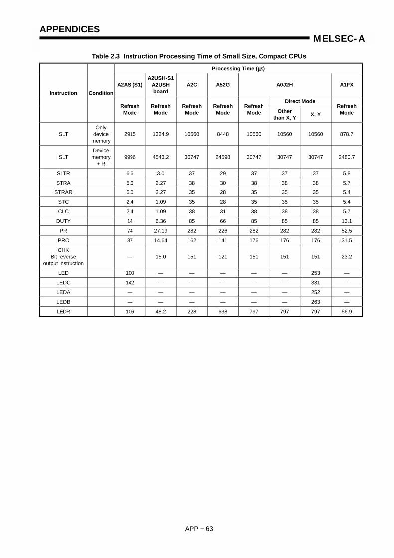
APPENDICES
APP − 63
MELSEC-A
Table 2.3 Instruction Processing Time of Small Size, Compact CPUs
Processing Time (µµµµs)
A2AS (S1)A2USH-S1
A2USHboard
A2C A52G A0J2H A1FX
Direct ModeInstruction Condition
RefreshMode
RefreshMode
RefreshMode
RefreshMode
RefreshMode Other
than X, Y X, YRefreshMode
SLTOnly
devicememory
2915 1324.9 10560 8448 10560 10560 10560 878.7
SLTDevice
memory+ R
9996 4543.2 30747 24598 30747 30747 30747 2480.7
SLTR 6.6 3.0 37 29 37 37 37 5.8
STRA 5.0 2.27 38 30 38 38 38 5.7
STRAR 5.0 2.27 35 28 35 35 35 5.4
STC 2.4 1.09 35 28 35 35 35 5.4
CLC 2.4 1.09 38 31 38 38 38 5.7
DUTY 14 6.36 85 66 85 85 85 13.1
PR 74 27.19 282 226 282 282 282 52.5
PRC 37 14.64 162 141 176 176 176 31.5
CHKBit reverse
output instruction— 15.0 151 121 151 151 151 23.2
LED 100 — — — — — 253 —
LEDC 142 — — — — — 331 —
LEDA — — — — — — 252 —
LEDB — — — — — — 263 —
LEDR 106 48.2 228 638 797 797 797 56.9
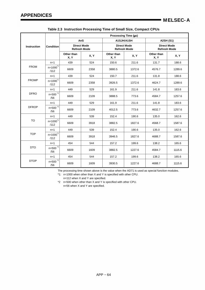
APPENDICES
APP − 64
MELSEC-A
Table 2.3 Instruction Processing Time of Small Size, Compact CPUs
Processing Time (µµµµs)
AnS A1SJH/A1SH A2SH (S1)
Direct ModeRefresh Mode
Direct ModeRefresh Mode
Direct ModeRefresh Mode
Instruction Condition
Other thanX, Y X, Y Other than
X, Y X, Y Other thanX, Y X, Y
n=1 439 524 150.6 211.6 131.7 188.6FROM n=1000
/112 6609 2358 3880.5 1372.6 4576.7 1289.6
n=1 439 524 150.7 211.6 131.8 188.6FROMP n=1000
/112 6609 2358 3926.5 1372.6 4624.7 1289.6
n=1 449 529 161.9 211.6 141.8 183.6DFRO n=500
/56 6609 2109 3888.5 773.6 4584.7 1257.6
n=1 449 529 161.9 211.6 141.8 183.6DFROP n=500
/56 6609 2109 4012.5 773.6 4632.7 1257.6
n=1 449 539 152.4 190.6 135.0 162.6TO n=1000
/112 6609 3918 3882.5 1827.6 4568.7 1587.6
n=1 449 539 152.4 190.6 135.0 162.6TOP n=1000
/112 6609 3918 3946.5 1827.6 4688.7 1587.6
n=1 454 544 157.2 199.6 138.2 165.6DTO n=500
/56 6609 1609 3882.5 1227.6 4584.7 1115.6
n=1 454 544 157.2 199.6 138.2 165.6DTOP n=500
/56 6609 1609 3930.5 1227.6 4688.7 1115.6
The processing time shown above is the value when the AD71 is used as special function modules.*1: n=1000 when other than X and Y is specified with other CPU.
n=112 when X and Y are specified.*2 n=500 when other than X and Y is specified with other CPU.
n=56 when X and Y are specified.
*1
*1
*2
*2
*1
*1
*2
*2
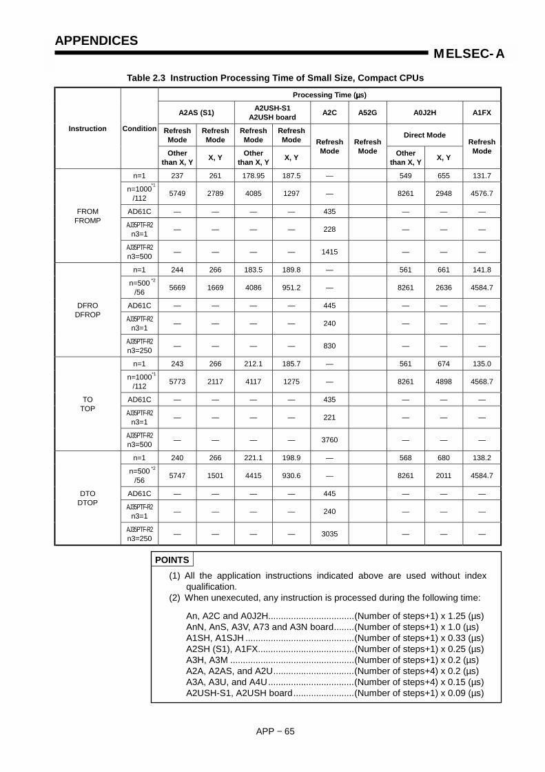
APPENDICES
APP − 65
MELSEC-A
Table 2.3 Instruction Processing Time of Small Size, Compact CPUs
Processing Time (µµµµs)
A2AS (S1) A2USH-S1A2USH board A2C A52G A0J2H A1FX
RefreshMode
RefreshMode
RefreshMode
RefreshMode Direct Mode
Instruction Condition
Otherthan X, Y X, Y Other
than X, Y X, Y
RefreshMode
RefreshMode Other
than X, Y X, Y
RefreshMode
n=1 237 261 178.95 187.5 — 549 655 131.7
n=1000/112 5749 2789 4085 1297 — 8261 2948 4576.7
AD61C — — — — 435 — — —
AJ35PTF-R2n3=1 — — — — 228 — — —
FROMFROMP
AJ35PTF-R2n3=500 — — — — 1415 — — —
n=1 244 266 183.5 189.8 — 561 661 141.8
n=500/56 5669 1669 4086 951.2 — 8261 2636 4584.7
AD61C — — — — 445 — — —
AJ35PTF-R2n3=1 — — — — 240 — — —
DFRODFROP
AJ35PTF-R2n3=250 — — — — 830 — — —
n=1 243 266 212.1 185.7 — 561 674 135.0
n=1000/112 5773 2117 4117 1275 — 8261 4898 4568.7
AD61C — — — — 435 — — —
AJ35PTF-R2n3=1 — — — — 221 — — —
TOTOP
AJ35PTF-R2n3=500 — — — — 3760 — — —
n=1 240 266 221.1 198.9 — 568 680 138.2
n=500/56 5747 1501 4415 930.6 — 8261 2011 4584.7
AD61C — — — — 445 — — —
AJ35PTF-R2n3=1 — — — — 240 — — —
DTODTOP
AJ35PTF-R2n3=250 — — — — 3035 — — —
POINTS(1) All the application instructions indicated above are used without index
qualification.(2) When unexecuted, any instruction is processed during the following time:
An, A2C and A0J2H..................................(Number of steps+1) x 1.25 (µs)AnN, AnS, A3V, A73 and A3N board........(Number of steps+1) x 1.0 (µs)A1SH, A1SJH ...........................................(Number of steps+1) x 0.33 (µs)A2SH (S1), A1FX......................................(Number of steps+1) x 0.25 (µs)A3H, A3M .................................................(Number of steps+1) x 0.2 (µs)A2A, A2AS, and A2U................................(Number of steps+4) x 0.2 (µs)A3A, A3U, and A4U..................................(Number of steps+4) x 0.15 (µs)A2USH-S1, A2USH board........................(Number of steps+1) x 0.09 (µs)
*1
*2
*1
*2

APPENDICES
APP − 66
MELSEC-A
2.2 Instruction Processing Time of CPUs
(1) Sequence instructions
Table 2.4 Instruction Processing Time of CPUs
Processing Time (µµµµs)
An AnN, A3V, A73,A3N Board A3H, A3M A2A,
A2U
A3A,A3U,A4U
Instruction Condition (Device)
D R D R D R R
X 2.3 1.0 2.3 2.0 0.20 0.20 0.15LD, LDIAND, ANIOR, ORI Y, M, L, B, F, T, C 1.3 1.0 1.0 0.20 0.20 0.20 0.15
ANBORB 1.3 1.0 1.0 0.20 0.20 0.20 0.15
Unchanged(OFF → OFF, ON → ON) 2.3 1.0 2.3 0.35 0.35 0.40 0.30
YChanged (OFF → ON, ON → OFF) 2.3 1.0 2.3 2.0 0.40 0.40 0.30
Unchanged(OFF → OFF, ON → ON) 1.3 1.0 0.35 0.35 0.35 0.40 0.30L, S, B
M (other thanspecial M) Changed (OFF → ON, ON → OFF) 1.3 1.0 1.0 0.40 0.40 0.40 0.30
Special M 37 37 0.40 0.40 0.80 0.60
Unexecuted 66 61 61 62 62 2.8 5.0F
Executed 700 663 663 283 283 99 77
Instruction execution time 1.3 1.0 1.0 0.2 0.2 0.40 0.30
Unexecuted 1.30
38 forA3V
0 0 0 0.23 0.18
After time out 15 11 11 3.7 3.7 4.5 3.3
K 30 24 24 5.9 5.9 7.7 5.7
TProcessingtime at theexecutionof ENDinstruction
Exe-cuted Added
D 36 30 30 5.9 5.9 7.7 5.7
Instruction execution time 1.3 1.0 1.0 0.20 0.20 0.40 0.30
Unexecuted 1.3 0 0 0 0 0.27 0.20
Uncounted 14 0 0 0 0 0.27 0.20
After count out 14 0 0 0 0 0.27 0.20
K 28 25 25 3.8 3.8 4.2 3.1
OUT
CProcessingtime at theexecutionof ENDinstruction
Exe-cuted
AddedD 33 30 30 4.6 4.6 4.8 3.6
Unexecuted 2.3 1.0 2.3 0.35 0.35 0.40 0.30
Unchanged (ON → ON) 2.3 1.0 2.3 0.35 0.35 0.40 0.30YExecuted
Changed (OFF → ON) 2.3 1.0 2.3 2.0 0.40 0.40 0.30
Unexecuted 3.7 1.0 1.0 0.35 0.35 0.40 0.30
Unchanged (ON → ON) 41 1.0 1.0 0.35 0.35 0.40 0.30M, L, S, BExecuted
Changed (OFF → ON) 41 1.0 1.0 0.40 0.40 0.40 0.30
Unexecuted 3.0 3.0 0.80 0.80 0.80 0.60Special MB Executed 32 32 1.4 1.4 0.80 0.80
Unexecuted 3.7 3.0 3.0 0.80 0.80 2.0 1.5
SET
FExecuted 730 638 638 283 283 99 77
R: Refresh mode, D: Direct mode

APPENDICES
APP − 67
MELSEC-A
Table 2.4 Instruction Processing Time of CPUs
Processing Time (µµµµs)
An AnN, A3V, A73,A3N Board A3H, A3M A2A,
A2U
A3A,A3U,A4U
Instruction Condition (Device)
D R D R D R R
Unexecuted 2.3 1.0 2.3 0.35 0.35 0.40 0.30
Unchanged (ON → ON) 2.3 1.0 2.3 0.35 0.35 0.40 0.30YExecuted
Changed (OFF → ON) 2.3 1.0 2.3 2.0 0.40 0.40 0.30
Unexecuted 3.7 1.0 1.0 0.35 0.35 0.40 0.30
Unchanged (ON → ON) 41 1.0 1.0 0.35 0.35 0.40 0.30M, L, S, BExecuted
Changed (OFF → ON) 41 1.0 1.0 0.40 0.40 0.40 0.30
Unexecuted 3.0 3.0 0.80 0.80 0.80 0.60Special MB Executed 32 32 1.4 1.4 0.80 0.60
Unexecuted 3.7 3.0 3.0 0.80 0.80 2.0 1.5F
Executed 680 477 477 427 427 150 115
Unexecuted 3.7 3.0 3.0 0.80 0.80 1.4 1.1T, C
Executed 57 43 43 5.2 5.2 5.6 4.2
Unexecuted 3.7 3.0 3.0 0.80 0.80 1.4 1.1D, WA0, A1V, Z Executed 34 28 28 0.80 0.80 8.4 6.3
Unexecuted 3.7 3.0 3.0 0.80 0.80 1.4 1.1
RST
RExecuted 41 35 35 57 57 4.6 3.5
NOP 1.3 1.0 1.0 0.20 0.20 0.20 0.15
M9084 OFF 2400 2150 2150 1128 1128 435 327
FENDEND M9084 ON 2400
2060A3V:
17000A73:7600
2060A73:7600
988 988 285 214
Unexecuted 85 43 44 6.4 2.6 1.2 0.90Y
Executed 50 39 41 6.4 2.6 1.2 0.90
Unexecuted 84 43 43 2.6 2.6 1.2 0.90MC
M, LB, F Executed 49 39 39 2.6 2.6 1.2 0.90
MCR 35 26 26 1.2 1.2 0.60 0.45
Unexecuted 65 59 61 5.6 1.8 2.2 1.7
ON 68 62 63 5.6 1.8 2.2 1.7YExecuted
OFF 64 60 62 5.6 1.8 2.2 1.7
Unexecuted 64 59 59 1.8 1.8 2.2 1.7
ON 67 62 62 1.8 1.8 2.2 1.7
PLSPLF
M, LB, F Executed
OFF 63 61 61 1.8 1.8 2.2 1.7
R: Refresh mode, D: Direct mode
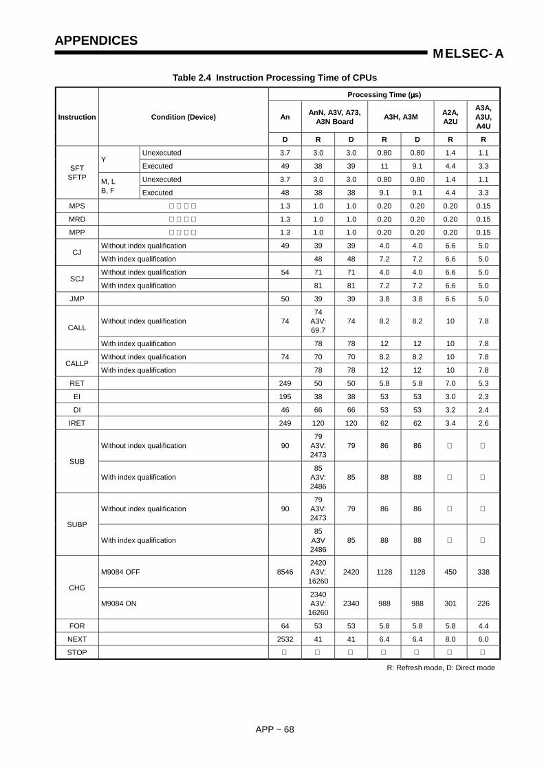
APPENDICES
APP − 68
MELSEC-A
Table 2.4 Instruction Processing Time of CPUs
Processing Time (µµµµs)
An AnN, A3V, A73,A3N Board A3H, A3M A2A,
A2U
A3A,A3U,A4U
Instruction Condition (Device)
D R D R D R R
Unexecuted 3.7 3.0 3.0 0.80 0.80 1.4 1.1Y
Executed 49 38 39 11 9.1 4.4 3.3
Unexecuted 3.7 3.0 3.0 0.80 0.80 1.4 1.1SFT
SFTP M, LB, F Executed 48 38 38 9.1 9.1 4.4 3.3
MPS 1.3 1.0 1.0 0.20 0.20 0.20 0.15
MRD 1.3 1.0 1.0 0.20 0.20 0.20 0.15
MPP 1.3 1.0 1.0 0.20 0.20 0.20 0.15
Without index qualification 49 39 39 4.0 4.0 6.6 5.0CJ
With index qualification 48 48 7.2 7.2 6.6 5.0
Without index qualification 54 71 71 4.0 4.0 6.6 5.0SCJ
With index qualification 81 81 7.2 7.2 6.6 5.0
JMP 50 39 39 3.8 3.8 6.6 5.0
Without index qualification 7474
A3V:69.7
74 8.2 8.2 10 7.8CALL
With index qualification 78 78 12 12 10 7.8
Without index qualification 74 70 70 8.2 8.2 10 7.8CALLP
With index qualification 78 78 12 12 10 7.8
RET 249 50 50 5.8 5.8 7.0 5.3
EI 195 38 38 53 53 3.0 2.3
DI 46 66 66 53 53 3.2 2.4
IRET 249 120 120 62 62 3.4 2.6
Without index qualification 9079
A3V:2473
79 86 86
SUB
With index qualification85
A3V:2486
85 88 88
Without index qualification 9079
A3V:2473
79 86 86
SUBP
With index qualification85
A3V2486
85 88 88
M9084 OFF 85462420A3V:
162602420 1128 1128 450 338
CHG
M9084 ON2340A3V:
162602340 988 988 301 226
FOR 64 53 53 5.8 5.8 5.8 4.4
NEXT 2532 41 41 6.4 6.4 8.0 6.0
STOP
R: Refresh mode, D: Direct mode
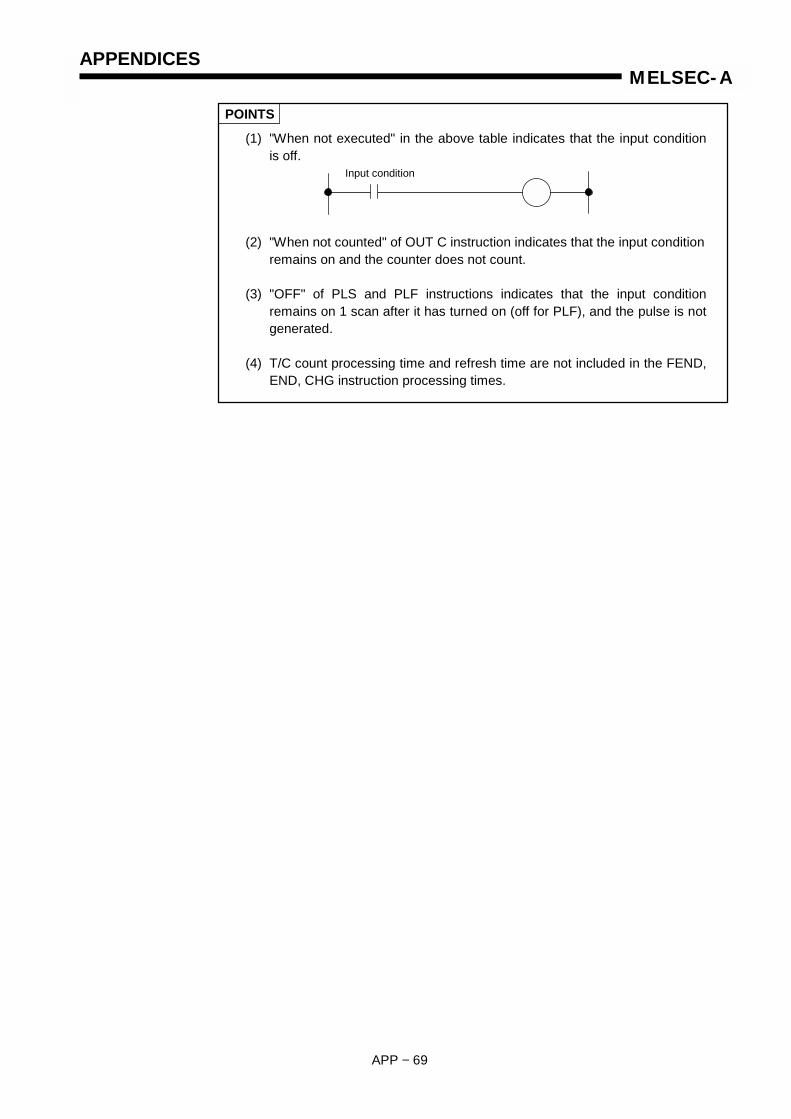
APPENDICES
APP − 69
MELSEC-A
POINTS
(1) "When not executed" in the above table indicates that the input conditionis off.
(2) "When not counted" of OUT C instruction indicates that the input conditionremains on and the counter does not count.
(3) "OFF" of PLS and PLF instructions indicates that the input conditionremains on 1 scan after it has turned on (off for PLF), and the pulse is notgenerated.
(4) T/C count processing time and refresh time are not included in the FEND,END, CHG instruction processing times.
Input condition

APPENDICES
APP − 70
MELSEC-A
(2) Basic instruction
Table 2.5 Instruction Processing Time of CPUs
Processing Time (µµµµs)
An AnN, A3V, A73A3N board A3H, A3M A2A, A2U A3A,
A3U, A4U
D DInstruction Condition
D R Otherthan X, Y X, Y
R Otherthan X, Y X, Y
R R
LD= 95 70 70 87 2.8 2.8 10 3.8 2.9
AND= 96 61 62 81 1.8 1.8 9.4 2.6 2.0
OR= 94 67 66 85 3.2 3.2 11 2.8 2.1
LDD= 238 133 134 119 157* 157* 180* 10 7.7
ANDD= 231 124 125 210 157* 157* 180* 5.9 4.4
ORD= 236 133 133 218 158* 158* 181* 6.3 4.7
LD<> 98 69 69 86 2.8 2.8 10 4.1 3.1
AND<> 92 60 60 79 1.8 1.8 9.4 2.6 2.0
OR<> 96 66 66 84 3.2 3.2 11 2.8 2.1
LDD<> 235 131 132 217 158* 158* 181* 10 7.7
ANDD<> 239 129 129 215 158* 158* 181* 5.9 4.4
ORD<> 234 129 129 214 161* 161* 184* 6.1 4.6
LD> 96 67 67 84 2.8 2.8 10 4.1 3.1
AND> 92 60 60 79 1.8 1.8 9.4 2.6 2.0
OR> 98 66 65 83 3.2 3.2 11 2.8 2.1
LDD> 238 133 133 219 158* 158* 181* 9.7 7.3
ANDD> 240 131 131 217 158* 158* 181* 5.8 4.4
ORD> 236 131 130 219 161* 161* 184* 6.0 4.5
LD>= 100 71 71 88 2.8 2.8 10 4.1 3.1
AND>= 94 61 61 81 1.8 1.8 9.4 2.6 2.0
OR>= 100 69 68 86 3.2 3.2 11 2.8 2.1
LDD>= 243 137 137 222 160* 158* 181* 9.7 7.3
ANDD>= 238 127 128 213 158* 158* 181* 5.8 4.4
ORD>= 246 137 136 221 161* 161* 183* 6.0 4.5
LD< 96 69 69 86 2.8 2.8 10 4.1 3.1
AND< 92 59 60 79 1.8 1.8 9.4 2.6 2.0
OR< 96 66 65 84 3.2 3.2 11 2.8 2.1
LDD< 238 133 133 219 159 159 182 9.7 7.3
ANDD< 241 131 131 217 158 158 181 5.8 4.4
ORD< 236 131 130 215 160 160 183 6.0 4.5
LD<= 100 71 71 88 2.8 2.8 10 4.1 3.1
AND<= 94 61 61 80 1.8 1.8 9.4 2.6 2.0
OR<= 100 69 68 86 3.2 3.2 11 2.8 2.1
LDD<= 244 137 136 222 158* 160* 181* 9.7 7.3
ANDD<= 238 127 128 213 158* 158* 181* 5.8 4.4
ORD<= 246 137 136 221 161* 161* 184* 6.0 4.5
R: Refresh mode, D: Direct mode* With an A3M, processing time will be 20 µs longer than the indicated time.
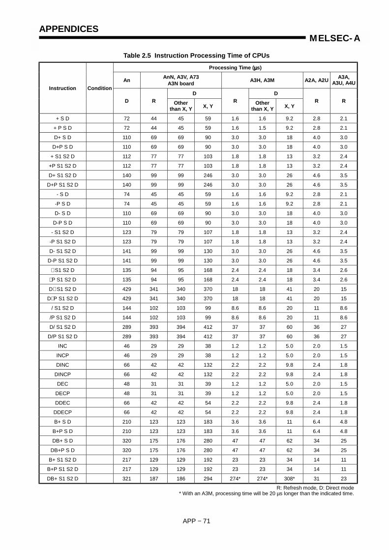
APPENDICES
APP − 71
MELSEC-A
Table 2.5 Instruction Processing Time of CPUs
Processing Time (µµµµs)
An AnN, A3V, A73A3N board A3H, A3M A2A, A2U A3A,
A3U, A4U
D DInstruction Condition
D R Otherthan X, Y X, Y
R Otherthan X, Y X, Y
R R
+ S D 72 44 45 59 1.6 1.6 9.2 2.8 2.1
+ P S D 72 44 45 59 1.6 1.5 9.2 2.8 2.1
D+ S D 110 69 69 90 3.0 3.0 18 4.0 3.0
D+P S D 110 69 69 90 3.0 3.0 18 4.0 3.0
+ S1 S2 D 112 77 77 103 1.8 1.8 13 3.2 2.4
+P S1 S2 D 112 77 77 103 1.8 1.8 13 3.2 2.4
D+ S1 S2 D 140 99 99 246 3.0 3.0 26 4.6 3.5
D+P S1 S2 D 140 99 99 246 3.0 3.0 26 4.6 3.5
- S D 74 45 45 59 1.6 1.6 9.2 2.8 2.1
-P S D 74 45 45 59 1.6 1.6 9.2 2.8 2.1
D- S D 110 69 69 90 3.0 3.0 18 4.0 3.0
D-P S D 110 69 69 90 3.0 3.0 18 4.0 3.0
- S1 S2 D 123 79 79 107 1.8 1.8 13 3.2 2.4
-P S1 S2 D 123 79 79 107 1.8 1.8 13 3.2 2.4
D- S1 S2 D 141 99 99 130 3.0 3.0 26 4.6 3.5
D-P S1 S2 D 141 99 99 130 3.0 3.0 26 4.6 3.5
∗ S1 S2 D 135 94 95 168 2.4 2.4 18 3.4 2.6
∗ P S1 S2 D 135 94 95 168 2.4 2.4 18 3.4 2.6
D∗ S1 S2 D 429 341 340 370 18 18 41 20 15
D∗ P S1 S2 D 429 341 340 370 18 18 41 20 15
/ S1 S2 D 144 102 103 99 8.6 8.6 20 11 8.6
/P S1 S2 D 144 102 103 99 8.6 8.6 20 11 8.6
D/ S1 S2 D 289 393 394 412 37 37 60 36 27
D/P S1 S2 D 289 393 394 412 37 37 60 36 27
INC 46 29 29 38 1.2 1.2 5.0 2.0 1.5
INCP 46 29 29 38 1.2 1.2 5.0 2.0 1.5
DINC 66 42 42 132 2.2 2.2 9.8 2.4 1.8
DINCP 66 42 42 132 2.2 2.2 9.8 2.4 1.8
DEC 48 31 31 39 1.2 1.2 5.0 2.0 1.5
DECP 48 31 31 39 1.2 1.2 5.0 2.0 1.5
DDEC 66 42 42 54 2.2 2.2 9.8 2.4 1.8
DDECP 66 42 42 54 2.2 2.2 9.8 2.4 1.8
B+ S D 210 123 123 183 3.6 3.6 11 6.4 4.8
B+P S D 210 123 123 183 3.6 3.6 11 6.4 4.8
DB+ S D 320 175 176 280 47 47 62 34 25
DB+P S D 320 175 176 280 47 47 62 34 25
B+ S1 S2 D 217 129 129 192 23 23 34 14 11
B+P S1 S2 D 217 129 129 192 23 23 34 14 11
DB+ S1 S2 D 321 187 186 294 274* 274* 308* 31 23
R: Refresh mode, D: Direct mode* With an A3M, processing time will be 20 µs longer than the indicated time.

APPENDICES
APP − 72
MELSEC-A
Table 2.5 Instruction Processing Time of CPUs
Processing Time (µµµµs)
An AnN, A3V, A73A3N board A3H, A3M A2A, A2U A3A,
A3U, A4U
D DInstruction Condition
D R Otherthan X, Y X, Y
R Otherthan X, Y X, Y
R R
DB+P S1 S2 D 321 187 186 294 274* 274* 308* 31 23
B- S D 210 125 125 185 3.6 3.6 11 6.2 4.7
B-P S D 210 125 125 185 3.6 3.6 11 6.2 4.7
DB- S D 318 175 175 208 47 47 6.2 32 24
DB-P S D 318 175 175 280 47 47 6.2 32 24
B- S1 S2 D 212 133 133 203 23 23 34 14 11
B-P S1 S2 D 212 133 133 203 23 23 34 14 11
DB- S1 S2 D 322 185 186 294 261* 261* 306* 29 22
DB-P S1 S2 D 322 185 186 294 261* 261* 306* 29 22
B∗ S1 S2 D 410 299 300 358 11 11 22 14 11
B∗ P S1 S2 D 410 299 300 358 11 11 22 14 11
DB∗ S1 S2 D 1158 941 939 1044 693* 693* 738* 89 67
DB∗ P S1 S2 D 1158 941 939 1044 693* 693* 738* 89 67
B/ S1 S2 D 422 235 236 274 25 25 40 11 8.0
B/P S1 S2 D 422 235 236 274 25 25 40 11 8.0
DB/ S1 S2 D 998 896 894 954 748* 748* 793* 62 47
DB/P S1 S2 D 998 896 894 954 748* 748* 793* 62 47
BCD 110 82 83 90 1.6 1.6 9.2 3.0 2.3
BCDP 110 82 83 90 1.6 1.6 9.2 3.0 2.3
DBCD 329 219 220 284 9.4 9.4 25 13 9.5
DBCDP 329 219 220 284 9.4 9.4 25 13 9.5
BIN 104 79 78 86 1.6 1.6 9.2 3.0 2.3
BINP 104 79 78 86 1.6 1.6 9.2 3.0 2.3
DBIN 311 215 216 280 3.6 3.6 19 6.0 4.5
DBINP 311 215 216 280 3.6 3.6 19 6.0 4.5
MOV 72 47 47 57 1.2 1.2 8.8 1.2 0.9
MOVP 72 47 47 57 1.2 1.2 8.8 1.2 0.9
DMOV 104 67 67 87 2.0 2.0 17 3.2 2.4
DMOVP 104 67 67 87 2.0 2.0 17 3.2 2.4
XCH 102 60 61 84 1.8 1.8 9.4 2.8 2.1
XCHP 102 60 61 84 1.8 1.8 9.4 2.8 2.1
DXCH 170 107 107 141 3.6 3.6 19 4.2 3.2
DXCHP 170 107 107 141 3.6 3.6 19 4.2 3.2
CML 68 43 43 57 1.4 1.4 9.0 2.4 1.8
CMLP 68 43 43 57 1.4 1.4 9.0 2.4 1.8
DCML 130 74 74 108 2.6 2.6 18 3.2 2.4
DCMLP 130 74 75 108 2.6 2.6 18 3.2 2.4
BMOV S D n n=96 7498 699 400 7144 132 132 862 72 54
R: Refresh mode, D: Direct mode* With an A3M, processing time will be 20 µs longer than the indicated time.

APPENDICES
APP − 73
MELSEC-A
Table 2.5 Instruction Processing Time of CPUs
Processing Time (µµµµs)
An AnN, A3V, A73A3N board A3H, A3M A2A, A2U A3A,
A3U, A4U
D DInstruction Condition
D R Otherthan X, Y X, Y
R Otherthan X, Y X, Y
R R
BMOVP S D n n=96 7498 699 400 7144 132 132 862 72 54
FMOV S D n n=96 1118 229 228 1029 66 66 435 32 24
FMOVP S D n n=96 1118 229 228 1029 66 66 435 32 24
R: Refresh mode, D: Direct mode
POINTS
(1) All the basic instructions indicated above are used without indexqualification.
(2) When unexecuted, any instruction is processed during the following time:
An................................................... (Number of steps + 1) x 1.3 (µs)AnN, A3V, A73 and A3N board ..... (Number of steps + 1) x 1.0 (µs)A3H and A3M ................................ (Number of steps + 1) x 0.2 (µs)A2A and A2U.................................(Number of steps + 4) x 0.2 (µs)A3A, A3U and A4U........................ (Number of steps + 4) x 0.15 (µs)

APPENDICES
APP − 74
MELSEC-A
(3) Application instructions
Table 2.6 Instruction Processing Time of CPUs
Processing Time (µµµµs)
An AnN, A3V, A73A3N Board A3H, A3M A2A, A2U A3A
A3U, A4U
D DInstruction Condition
D R OtherthanX, Y
X, YR Other
thanX, Y
X, YR R
WAND S D 90 60 59 72 1.6 1.6 9.2 2.8 2.1
WANDP S D 90 60 59 72 1.6 1.6 9.2 2.8 2.1
DAND 276 140 139 240 27 27 43 13 9.5
DANDP 276 140 139 240 27 27 43 13 9.5
WAND S1 S2 D 179 96 96 152 21 21 32 7.6 5.7
WANDP S1 S2 D 179 96 96 152 21 21 32 7.6 5.7
WOR S D 90 61 60 72 1.6 1.6 9.2 2.8 2.1
WORP S D 90 61 60 72 1.6 1.6 9.2 2.8 2.1
DOR 276 140 139 240 27 27 43 13 9.5
DORP 276 140 139 240 27 27 43 13 9.5
WOR S1 S2 D 176 97 96 152 21 21 32 7.6 5.7
WORP S1 S2 D 176 97 96 152 21 21 32 7.6 5.7
WXOR S D 91 60 59 72 1.6 1.6 9.2 2.8 2.1
WXORP S D 91 60 59 72 1.6 1.6 9.2 2.8 2.1
DXOR 274 140 139 240 27 27 43 13 9.5
DXORP 274 140 139 240 27 27 43 13 9.5
WXOR S1 S2 D 178 97 96 152 21 21 32 7.6 5.7
WXORP S1 S2 D 178 97 96 152 21 21 32 7.6 5.7
WXNR S D 89 64 62 74 1.6 1.6 9.2 3.0 2.3
WXNRP S D 89 64 62 74 1.6 1.6 9.2 3.0 2.3
DXNR 277 142 140 241 27 27 43 15 11
DXNRP 277 142 140 241 27 27 43 15 11
WXNR S1 S2 D 177 98 96 152 21 21 32 7.8 5.9
WXNRP S1 S2 D 177 98 96 152 21 21 32 7.8 5.9
NEG 105 50 49 86 14 14 18 8.6 6.5
NEGP 105 50 49 86 14 14 18 8.6 6.5
ROR n n=5 66 52 51 51 4.8 4.8 4.8 5.8 4.4
RORP n n=5 66 52 51 51 4.8 4.8 4.8 5.8 4.4
RCR n n=5 74 59 59 59 6.8 6.8 6.8 6.4 4.8
RCRP n n=5 74 59 59 59 6.8 6.8 6.8 6.4 4.8
R: Refresh mode, D: Direct mode
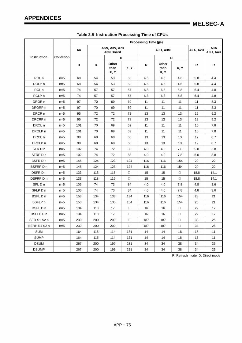
APPENDICES
APP − 75
MELSEC-A
Table 2.6 Instruction Processing Time of CPUs
Processing Time (µµµµs)
An AnN, A3V, A73A3N Board A3H, A3M A2A, A2U A3A
A3U, A4U
D DInstruction Condition
D R OtherthanX, Y
X, YR Other
thanX, Y
X, YR R
ROL n n=5 68 54 53 53 4.6 4.6 4.6 5.8 4.4
ROLP n n=5 68 54 53 53 4.6 4.6 4.6 5.8 4.4
RCL n n=5 74 57 57 57 6.8 6.8 6.8 6.4 4.8
RCLP n n=5 74 57 57 57 6.8 6.8 6.8 6.4 4.8
DROR n n=5 97 70 69 69 11 11 11 11 8.3
DRORP n n=5 97 70 69 69 11 11 11 11 8.3
DRCR n n=5 95 72 72 72 13 13 13 12 9.2
DRCRP n n=5 95 72 72 72 13 13 13 12 9.2
DROL n n=5 101 70 69 69 11 11 11 10 7.8
DROLP n n=5 101 70 69 69 11 11 11 10 7.8
DRCL n n=5 98 68 68 68 13 13 13 12 8.7
DRCLP n n=5 98 68 68 68 13 13 13 12 8.7
SFR D n n=5 102 74 72 83 4.0 4.0 7.8 5.0 3.8
SFRP D n n=5 102 74 72 83 4.0 4.0 7.8 5.0 3.8
BSFR D n n=5 145 124 123 124 116 116 154 29 22
BSFRP D n n=5 145 124 123 124 116 116 154 29 22
DSFR D n n=5 133 118 116 15 15 18.8 14.1
DSFRP D n n=5 133 118 116 15 15 18.8 14.1
SFL D n n=5 106 74 73 84 4.0 4.0 7.8 4.8 3.6
SFLP D n n=5 106 74 73 84 4.0 4.0 7.8 4.8 3.6
BSFL D n n=5 158 134 133 134 116 116 154 28 21
BSFLP n n=5 158 134 133 134 116 116 154 28 21
DSFL D n n=5 134 118 17 16 16 22 17
DSFLP D n n=5 134 118 17 16 16 22 17
SER S1 S2 n n=5 230 200 200 187 187 33 25
SERP S1 S2 n n=5 230 200 200 187 187 33 25
SUM 164 115 114 131 14 14 18 15 11
SUMP 164 115 114 131 14 14 18 15 11
DSUM 267 200 199 231 34 34 38 34 25
DSUMP 267 200 199 231 34 34 38 34 25
R: Refresh mode, D: Direct mode
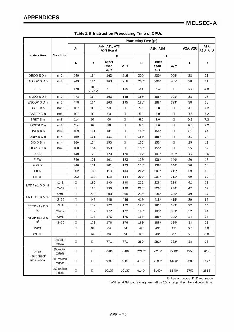
APPENDICES
APP − 76
MELSEC-A
Table 2.6 Instruction Processing Time of CPUs
Processing Time (µµµµs)
An AnN, A3V, A73A3N Board A3H, A3M A2A, A2U A3A
A3U, A4U
D DInstruction Condition
D R OtherthanX, Y
X, YR Other
thanX, Y
X, YR R
DECO S D n n=2 249 164 163 216 200* 200* 205* 28 21
DECOP S D n n=2 249 164 163 216 200* 200* 205* 28 21
SEG 170 91A3V:92 91 155 3.4 3.4 11 6.4 4.8
ENCO S D n n=2 478 164 163 195 188* 188* 193* 38 28
ENCOP S D n n=2 478 164 163 195 188* 188* 193* 38 28
BSET D n n=5 107 90 90 5.0 5.0 9.6 7.2
BSETP D n n=5 107 90 90 5.0 5.0 9.6 7.2
BRST D n n=5 114 97 96 5.0 5.0 9.6 7.2
BRSTP D n n=5 114 97 96 5.0 5.0 9.6 7.2
UNI S D n n=4 159 131 131 155* 155* 31 24
UNIP S D n n=4 159 131 131 155* 155* 31 24
DIS S D n n=4 180 154 153 155* 155* 25 19
DISP S D n n=4 180 154 153 155* 155* 25 19
ASC 140 120 120 120 107* 107* 107* 3.4 2.6
FIFW 340 101 101 123 136* 136* 140* 20 15
FIFWP 340 101 101 123 136* 136* 140* 20 15
FIFR 202 118 118 134 207* 207* 211* 69 52
FIFRP 202 118 118 134 207* 207* 211* 69 52
n2=1 190 190 190 228* 228* 228* 42 32LRDP n1 S D n2
n2=32 190 190 190 228* 228* 228* 42 32
n2=1 200 200 200 236* 236* 236* 49 37LWTP n1 D S n2
n2=32 446 446 446 415* 415* 415* 89 66
n3=1 172 172 172 183* 183* 183* 32 24RFRP n1 n2 Dn3 n3=32 172 172 172 183* 183* 183* 32 24
n3=1 176 176 176 185* 185* 185* 34 26RTOP n1 n2 Sn3 n3=32 176 176 176 185* 185* 185* 34 26
WDT 64 64 64 49* 49* 49* 5.0 3.8
WDTP 64 64 64 49* 49* 49* 5.0 3.8
1 conditioncontact 771 771 282* 282* 282* 33 25
50 conditioncontacts 3380 3380 2210* 2210* 2210* 1257 943
100 conditioncontacts 6887 6887 4180* 4180* 4180* 2503 1877
CHKFault checkinstruction
150 conditioncontacts 10137 10137 6140* 6140* 6140* 3753 2815
R: Refresh mode, D: Direct mode* With an A3M, processing time will be 20µs longer than the indicated time.

APPENDICES
APP − 77
MELSEC-A
Table 2.6 Instruction Processing Time of CPUs
Processing Time (µµµµs)
An AnN, A3V, A73A3N Board A3H, A3M A2A, A2U A3A
A3U, A4UD DInstruction Condition
D R OtherthanX, Y
X, YR Other
thanX, Y
X, YR R
SLTOnly
devicememory
8448 8448 8448 4100* 4100* 4100* 2915 2186
SLTDevice
memory+R
24598 24598 24598 10400* 10400* 10400* 9996 7497
SLTR 29 29 29 53* 53* 53* 6.6 5.0
STRA 30 30 30 52* 52* 52* 5.0 3.8
STRAR 28 28 28 52* 52* 52* 5.0 3.8
STC 28 28 28 1.2 1.2 1.2 2.4 1.8
CLC 31 31 31 1.2 1.2 1.2 2.4 1.8
DUTY 68 68 68 121* 121* 121 14 11
PR 226 226 226 183* 183* 183* 74 59
PRC 141 141 141 145 145 145 37 31
CHKBit reverse
output instruction 121 121 121
LED 170 203 203 203 282* 282* 282* 100 75
LEDC 210 265 265 265 320* 320* 320* 142 109
LEDA 170 202 202 202 262* 262* 262*
LEDB 172 211 211 211 262* 262* 262*
LEDR 520 638 638 638 460* 460* 460* 106 80
R: Refresh mode, D: Direct mode* With an A3M, processing time will be 20µs longer than the indicated time.
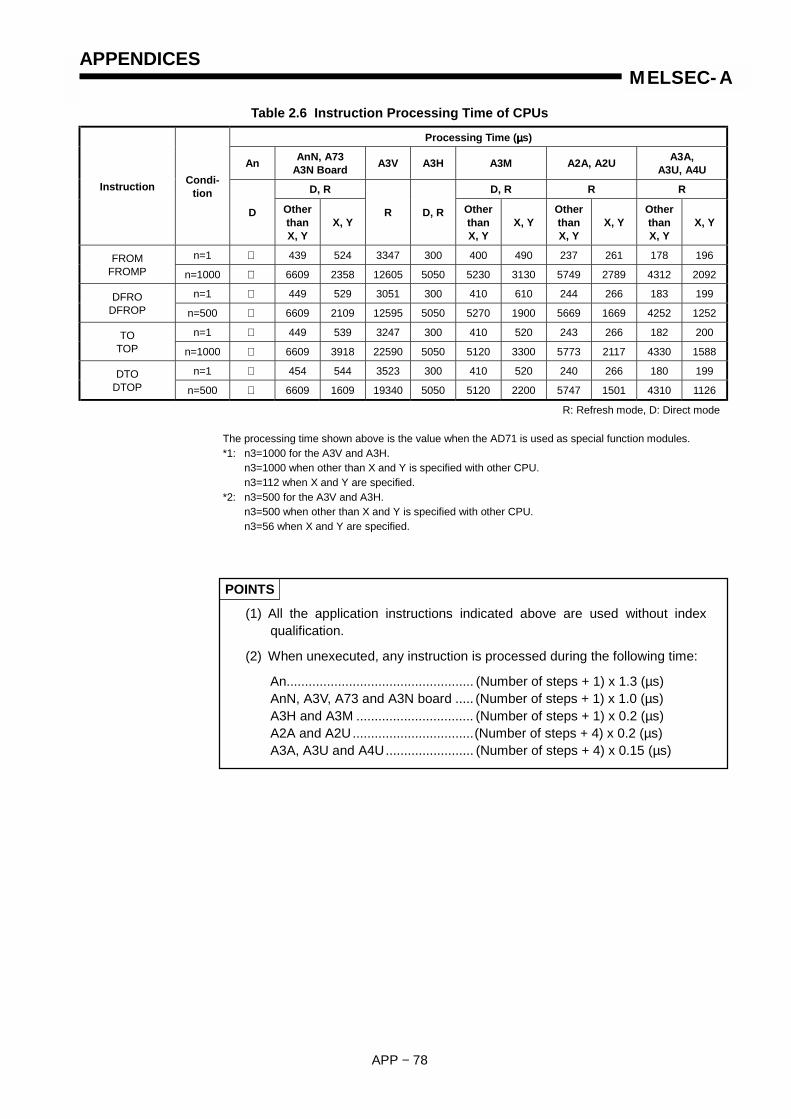
APPENDICES
APP − 78
MELSEC-A
Table 2.6 Instruction Processing Time of CPUs
Processing Time (µµµµs)
An AnN, A73A3N Board A3V A3H A3M A2A, A2U A3A,
A3U, A4U
D, R D, R R RInstruction Condi-tion
D OtherthanX, Y
X, YR D, R Other
thanX, Y
X, YOtherthanX, Y
X, YOtherthanX, Y
X, Y
n=1 439 524 3347 300 400 490 237 261 178 196FROMFROMP n=1000 6609 2358 12605 5050 5230 3130 5749 2789 4312 2092
n=1 449 529 3051 300 410 610 244 266 183 199DFRODFROP n=500 6609 2109 12595 5050 5270 1900 5669 1669 4252 1252
n=1 449 539 3247 300 410 520 243 266 182 200TOTOP n=1000 6609 3918 22590 5050 5120 3300 5773 2117 4330 1588
n=1 454 544 3523 300 410 520 240 266 180 199DTODTOP n=500 6609 1609 19340 5050 5120 2200 5747 1501 4310 1126
R: Refresh mode, D: Direct mode
The processing time shown above is the value when the AD71 is used as special function modules.*1: n3=1000 for the A3V and A3H.
n3=1000 when other than X and Y is specified with other CPU.n3=112 when X and Y are specified.
*2: n3=500 for the A3V and A3H.n3=500 when other than X and Y is specified with other CPU.n3=56 when X and Y are specified.
POINTS
(1) All the application instructions indicated above are used without indexqualification.
(2) When unexecuted, any instruction is processed during the following time:
An................................................... (Number of steps + 1) x 1.3 (µs)AnN, A3V, A73 and A3N board ..... (Number of steps + 1) x 1.0 (µs)A3H and A3M ................................ (Number of steps + 1) x 0.2 (µs)A2A and A2U.................................(Number of steps + 4) x 0.2 (µs)A3A, A3U and A4U........................ (Number of steps + 4) x 0.15 (µs)

APP - 79
MELSEC-AAPPENDICES
2.3 List of Instruction Processing Time of QCPU-A (A Mode)
The following table shows the instruction processing time of QCPU-A (A mode).
(1) Sequence instructions
Table 2.7 Instruction Processing Time of QCPU-A (A Mode)Instruction Processing Time (µs)
Instruction Condition (Device)QnCPU-A QnHCPU-A
X 0.079 0.034LD, LDIAND, ANIOR, ORI
Y, M, L, S, B, F, T, C 0.079 0.034
At no change (OFF OFF, ON ON) 0.158 0.068Y
At change (OFF ON, ON OFF) 0.158 0.068At no change (OFF OFF, ON ON) 0.158 0.068M (except for special M)
L S B At change (OFF ON, ON OFF) 0.158 0.068Special M 0.316 0.136
At no execution 1.11 0.480F
At execution 35.1 15.1Instruction execution time 0.158 0.068
Time for no execution 0.088 0.037After time elapsed 1.80 0.774
K 3.07 1.32T
ENDAt execution
At additionD 3.31 1.42
Instruction execution time 0.158 0.068Time for no execution 0.105 0.045
At no counting 0.105 0.045After counting up 0.105 0.045
K 1.67 0.720
OUT
CEND
At executionAt counting
D 1.91 0.823At no execution 0.158 0.068
At no change (ON ON) 0.158 0.068YAt execution
At change (OFF ON) 0.158 0.068At no execution 0.158 0.068
At no change (ON ON) 0.158 0.068
SETM, LS, B At execution
At change (OFF ON) 0.158 0.068
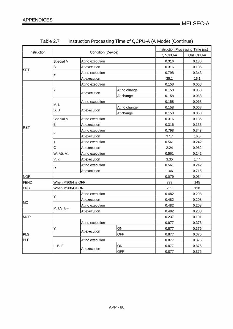
APP - 80
MELSEC-AAPPENDICES
Table 2.7 Instruction Processing Time of QCPU-A (A Mode) (Continue)Instruction Processing Time (µs)
Instruction Condition (Device)QnCPU-A QnHCPU-A
At no execution 0.316 0.136Special MB At execution 0.316 0.136
At no execution 0.798 0.343SET
FAt execution 35.1 15.1At no execution 0.158 0.068
At no change 0.158 0.068YAt execution
At change 0.158 0.068At no execution 0.158 0.068
At no change 0.158 0.068M, LS, B At execution
At change 0.158 0.068At no execution 0.316 0.136Special M
B At execution 0.316 0.136At no execution 0.798 0.343
FAt execution 37.7 16.3At no execution 0.561 0.242T
C At execution 2.24 0.962At no execution 0.561 0.242W, A0, A1
V, Z At execution 3.35 1.44At no execution 0.561 0.242
RST
RAt execution 1.66 0.715
NOP 0.079 0.034When M9084 is OFF 339 145FEND
END When M9084 is ON 253 110At no execution 0.482 0.208
YAt execution 0.482 0.208At no execution 0.482 0.208
MCM, LS, BF
At execution 0.482 0.208MCR 0.237 0.101
At no execution 0.877 0.376ON 0.877 0.376Y
At executionOFF 0.877 0.376
At no execution 0.877 0.376ON 0.877 0.376
PLSPLF
L, B, FAt execution
OFF 0.877 0.376
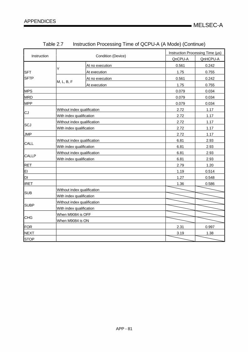
APP - 81
MELSEC-AAPPENDICES
Table 2.7 Instruction Processing Time of QCPU-A (A Mode) (Continue)Instruction Processing Time (µs)
Instruction Condition (Device)QnCPU-A QnHCPU-A
At no execution 0.561 0.242Y
At execution 1.75 0.755
At no execution 0.561 0.242SFTSFTP
M, L, B, FAt execution 1.75 0.755
MPS 0.079 0.034MRD 0.079 0.034MPP 0.079 0.034
Without index qualification 2.72 1.17CJ
With index qualification 2.72 1.17Without index qualification 2.72 1.17
SCJWith index qualification 2.72 1.17
JMP 2.72 1.17Without index qualification 6.81 2.93
CALLWith index qualification 6.81 2.93Without index qualification 6.81 2.93
CALLPWith index qualification 6.81 2.93
RET 2.79 1.20EI 1.19 0.514DI 1.27 0.548IRET 1.36 0.586
Without index qualificationSUB
With index qualificationWithout index qualification
SUBPWith index qualificationWhen M9084 is OFF
CHGWhen M9084 is ON
FOR 2.31 0.997NEXT 3.19 1.38STOP
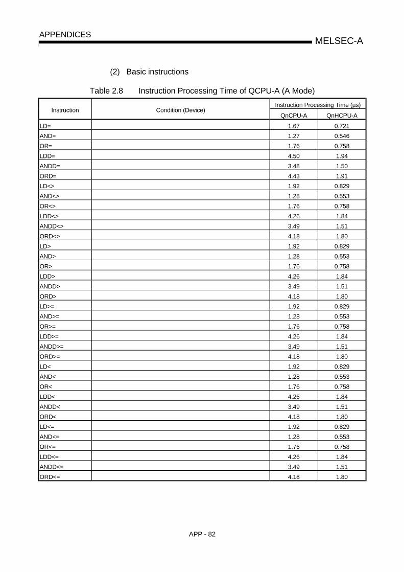
APP - 82
MELSEC-AAPPENDICES
(2) Basic instructions
Table 2.8 Instruction Processing Time of QCPU-A (A Mode)Instruction Processing Time (µs)
Instruction Condition (Device)QnCPU-A QnHCPU-A
LD= 1.67 0.721AND= 1.27 0.546OR= 1.76 0.758LDD= 4.50 1.94ANDD= 3.48 1.50ORD= 4.43 1.91LD<> 1.92 0.829AND<> 1.28 0.553OR<> 1.76 0.758LDD<> 4.26 1.84ANDD<> 3.49 1.51ORD<> 4.18 1.80LD> 1.92 0.829AND> 1.28 0.553OR> 1.76 0.758LDD> 4.26 1.84ANDD> 3.49 1.51ORD> 4.18 1.80LD>= 1.92 0.829AND>= 1.28 0.553OR>= 1.76 0.758LDD>= 4.26 1.84ANDD>= 3.49 1.51ORD>= 4.18 1.80LD< 1.92 0.829AND< 1.28 0.553OR< 1.76 0.758LDD< 4.26 1.84ANDD< 3.49 1.51ORD< 4.18 1.80LD<= 1.92 0.829AND<= 1.28 0.553OR<= 1.76 0.758LDD<= 4.26 1.84ANDD<= 3.49 1.51ORD<= 4.18 1.80

APP - 83
MELSEC-AAPPENDICES
Table 2.8 Instruction Processing Time of QCPU-A (A Mode) (Continue)Instruction Processing Time (µs)
Instruction Condition (Device)QnCPU-A QnHCPU-A
+ S D 1.11 0.480+P S D 1.11 0.480D+ S D 1.60 0.688D+P S D 1.60 0.688+ S1 S2 D 1.27 0.548+P S1 S2 D 1.27 0.548D+ S1 S2 D 1.83 0. 790D+P S1 S2 D 1.83 0.790- S D 1.11 0.480-P S D 1.11 0.480D- S D 1.60 0.688D-P S D 1.60 0.688- S1 S2 D 1.27 0.548-P S1 S2 D 1.27 0.548D- S1 S2 D 1.83 0.790D-P S1 S2 D 1.83 0.790S1 S2 D 1.36 0.586P S1 S2 D 1.36 0.586D S1 S2 D 7.97 3.43D P S1 S2 D 7.97 3.43/ S1 S2 D 4.38 1.89/P S1 S2 D 4.38 1.89D/ S1 S2 D 14.4 6.20D/P S1 S2 D 14.377 6.20INC 0.798 0.344INCP 0.798 0.344DINC 0.956 0.412DINCP 0.956 0.412DEC 0.798 0.344DECP 0.798 0.344DDEC 0.956 0.412DDECP 0.956 0.412B+ S D 2.55 1.10B+P S D 2.55 1.10DB+ S D 13.6 5.86DB+P S D 13.6 5.86B+ S1 S2 D 5.58 2.40B+P S1 S2 D 5.58 2.40DB+ S1 S2 D 12.4 5.32DB+P S1 S2 D 12.4 5.32

APP - 84
MELSEC-AAPPENDICES
Table 2.8 Instruction Processing Time of QCPU-A (A Mode) (Continue)Instruction Processing Time (µs)
Instruction Condition (Device)QnCPU-A QnHCPU-A
B- S D 2.47 1.07B-P S D 2.47 1.07DB- S D 12.7 5.48DB-P S D 12.7 5.48B- S1 S2 D 5.58 2.40B-P S1 S2 D 5.58 2.40DB- S1 S2 D 11.6 4.99DB-P S1 S2 D 11.6 4.99B S1 S2 D 5.58 2.40B P S1 S2 D 5.58 2.40DB S1 S2 D 35.5 15.3DB P S1 S2 D 35.5 15.3B/ S1 S2 D 4.38 1.89B/P S1 S2 D 4.38 1.89DB/ S1 S2 D 24.7 10.7DB/P S1 S2 D 24.7 10.7BCD 1.19 0.51BCDP 1.19 0.51DBCD 5.18 2.23DBCDP 5.18 2.23BIN 1.19 0.51BINP 1.19 0.51DBIN 2.39 1.03DBINP 2.39 1.03MOV 0.482 0.208MOVP 0.482 0.208DMOV 1.27 0.548DMOVP 1.27 0.548XCH 1.11 0.480XCHP 1.11 0.480DXCH 1.61 0.722DXCHP 1.61 0.722CML 0.956 0.412CMLP 0.956 0.412DCML 1.27 0.548DCMLP 1.27 0.548BMOV S D n n=96 28.7 12.4BMOVP S D n n=96 28.7 12.4FMOV S D n n=96 12.7 5.48FMOVP S D n n=96 12.7 5.48
POINTS(1) All the basic instructions indicated above are used without index qualification.(2) When unexecuted, any instruction is processed during the following time:
Q02CPU-A ........................................ (Number of steps + 1) × 0.079 (µs)Q02HCPU-A, Q06HCPU-A .............. (Number of steps + 1) × 0.034 (µs)

APP - 85
MELSEC-AAPPENDICES
(3) Application instructions
Table 2.9 Instruction Processing Time of QCPU-A (A Mode)Instruction Processing Time (µs)
Instruction Condition (Device)QnCPU-A QnHCPU-A
WAND S D 1.11 0.480WANDP S D 1.11 0.480DAND 5.18 2.23DANDP 5.18 2.23WAND S1 S2 D 3.03 1.30WANDP S1 S2 D 3.03 1.30WOR S D 1.11 0.480WORP S D 1.11 0.480DOR 5.18 2.23DORP 5.18 2.23WOR S1 S2 D 3.03 1.30WORP S1 S2 D 3.03 1.30WXOR S D 1.11 0.480WXORP S D 1.11 0.480DXOR 5.18 2.23DXORP 5.18 2.23WXOR S1 S2 D 3.03 1.30WXORP S1 S2 D 3.03 1.30WXNR S D 1.19 0.514WXNRP S D 1.19 0.514DXNR 5.98 2.58DXNRP 5.98 2.58WXNR S1 S2 D 3.11 1.34WXNRP S1 S2 D 3.11 1.34NEG 3.43 1.48NEGP 3.43 1.48

APP - 86
MELSEC-AAPPENDICES
Table 2.9 Instruction Processing Time of QCPU-A (A Mode) (Continue)Instruction Processing Time (µs)
Instruction Condition (Device)QnCPU-A QnHCPU-A
ROR n n=5 2.31 0.997RORP n n=5 2.31 0.997RCR n n=5 2.55 1.10RCRP n n=5 2.55 1.10ROL n n=5 2.31 0.997ROLP n n=5 2.31 0.997RCL n n=5 2.55 1.10RCLP n n=5 2.55 1.10DROR n n=5 4.38 1.89DRORP n n=5 4.38 1.89DRCR n n=5 4.78 2.06DRCRP n n=5 4.78 2.06DROL n n=5 3.99 1.72DROLP n n=5 3.99 1.72DRCL n n=5 4.78 2.06DRCLP n n=5 4.78 2.06SFR D n n=5 1.99 0.86SFRP D n n=5 1.99 0.86BSFR D n n=5 11.6 4.99BSFRP D n n=5 11.6 4.99DSFR D n n=5 7.49 3.23DSFRP D n n=5 7.49 3.23SFL D n n=5 1.91 0.82SFLP D n n=5 1.91 0.82BSFL D n n=5 11.1 4.80BSFLP D n n=5 11.1 4.80DSFL D n n=5 8.77 3.78DSFLP D n n=5 8.77 3.78SER S1 S2 n n=5 13.2 5.67SERP S1 S2 n n=5 13.2 5.67

APP - 87
MELSEC-AAPPENDICES
Instruc Table 2.9 Instruction Processing Time of QCPU-A (A Mode) (Continue)Instruction Processing Time (µs)
Instruction Condition (Device)QnCPU-A QnHCPU-A
SUM 5.98 2.58SUMP 5.98 2.58DSUM 13.6 5.59DSUMP 13.6 5.59DECO S D n n=2 11.1 4.80DECOP S D n n=2 11.1 4.80SEG 2.55 1.10ENCO S D n n=2 15.2 6.54ENCOP S D n n=2 15.2 6.54BSET D n n=5 3.82 1.65BSETP D n n=5 3.82 1.65BRST D n n=5 3.82 1.65BRSTP D n n=5 3.82 1.65UNI S D n n=4 12.4 5.32UNIP S D n n=4 12.4 5.32DIS S D n n=4 9.96 4.29DISP S D n n=4 9.96 4.29ASC 1.36 0.586FIFW 18.0 3.44FIFWP 7.98 3.44FIFR 27.5 11.8FIFRP 27.5 11.8
n2=1 33.0 27.4LRDP n1 S D n2
n2=32 33.0 27.4n2=1 34.9 29.0
LWTP n1 S D n2n2=32 54.6 45.3n3=1 14.5 12.0
RFRP n1 n2 D n3n3=32 14.5 12.0n3=1 15.5 12.9
RTOP n1 n2 S n3n3=32 15.5 12.9
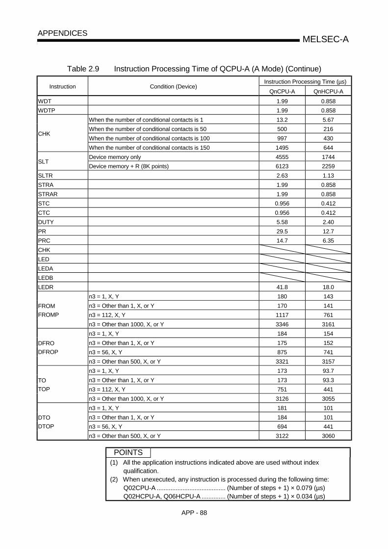
APP - 88
MELSEC-AAPPENDICES
Table 2.9 Instruction Processing Time of QCPU-A (A Mode) (Continue)Instruction Processing Time (µs)
Instruction Condition (Device)QnCPU-A QnHCPU-A
WDT 1.99 0.858WDTP 1.99 0.858
When the number of conditional contacts is 1 13.2 5.67When the number of conditional contacts is 50 500 216When the number of conditional contacts is 100 997 430
CHK
When the number of conditional contacts is 150 1495 644Device memory only 4555 1744
SLTDevice memory + R (8K points) 6123 2259
SLTR 2.63 1.13STRA 1.99 0.858STRAR 1.99 0.858STC 0.956 0.412CTC 0.956 0.412DUTY 5.58 2.40PR 29.5 12.7PRC 14.7 6.35CHKLEDLEDALEDBLEDR 41.8 18.0
n3 = 1, X, Y 180 143n3 = Other than 1, X, or Y 170 141n3 = 112, X, Y 1117 761
FROMFROMP
n3 = Other than 1000, X, or Y 3346 3161n3 = 1, X, Y 184 154n3 = Other than 1, X, or Y 175 152n3 = 56, X, Y 875 741
DFRODFROP
n3 = Other than 500, X, or Y 3321 3157n3 = 1, X, Y 173 93.7n3 = Other than 1, X, or Y 173 93.3n3 = 112, X, Y 751 441
TOTOP
n3 = Other than 1000, X, or Y 3126 3055n3 = 1, X, Y 181 101n3 = Other than 1, X, or Y 184 101n3 = 56, X, Y 694 441
DTODTOP
n3 = Other than 500, X, or Y 3122 3060
POINTS(1) All the application instructions indicated above are used without index
qualification.(2) When unexecuted, any instruction is processed during the following time:
Q02CPU-A ........................................ (Number of steps + 1) × 0.079 (µs)Q02HCPU-A, Q06HCPU-A .............. (Number of steps + 1) × 0.034 (µs)
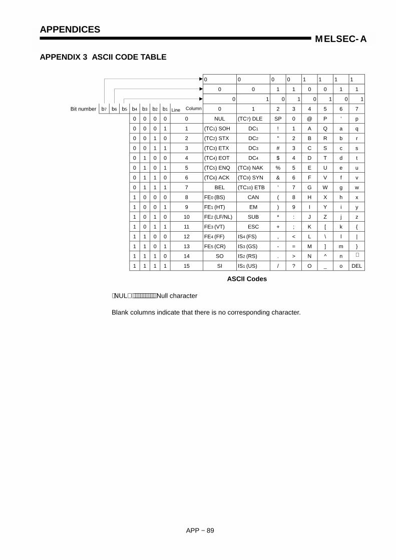
APPENDICES
APP − 89
MELSEC-A
APPENDIX 3 ASCII CODE TABLE
0 0 0 0 1 1 1 1
0 0 1 1 0 0 1 1
0 1 0 1 0 1 0 1
Bit number b7 b6 b5 b4 b3 b2 b1 Line Column 0 1 2 3 4 5 6 7
0 0 0 0 0 NUL (TC7) DLE SP 0 @ P ’ p
0 0 0 1 1 (TC1) SOH DC1 ! 1 A Q a q
0 0 1 0 2 (TC2) STX DC2 " 2 B R b r
0 0 1 1 3 (TC3) ETX DC3 # 3 C S c s
0 1 0 0 4 (TC4) EOT DC4 $ 4 D T d t
0 1 0 1 5 (TC5) ENQ (TC8) NAK % 5 E U e u
0 1 1 0 6 (TC6) ACK (TC9) SYN & 6 F V f v
0 1 1 1 7 BEL (TC10) ETB ’ 7 G W g w
1 0 0 0 8 FE0 (BS) CAN ( 8 H X h x
1 0 0 1 9 FE1 (HT) EM ) 9 I Y i y
1 0 1 0 10 FE2 (LF/NL) SUB * : J Z j z
1 0 1 1 11 FE3 (VT) ESC + ; K [ k {
1 1 0 0 12 FE4 (FF) IS4 (FS) , < L \ l |
1 1 0 1 13 FE5 (CR) IS3 (GS) - = M ] m }
1 1 1 0 14 SO IS2 (RS) . > N ^ n ∼
1 1 1 1 15 SI IS1 (US) / ? O _ o DEL
⟨NUL⟩ ⋅⋅⋅⋅⋅⋅⋅⋅⋅⋅⋅⋅⋅⋅ Null character
Blank columns indicate that there is no corresponding character.
ASCII Codes
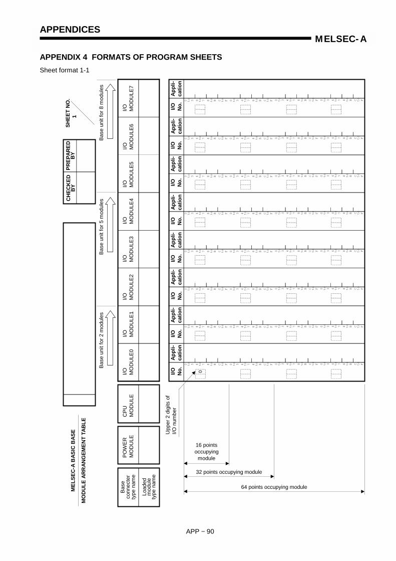
APPENDICES
APP − 90
MELSEC-A
APPENDIX 4 FORMATS OF PROGRAM SHEETSSheet format 1-1
Base
uni
t for
8 m
odul
es
to0 3 4 7 8 B C Fto
to
to
to0 3 4 7 8 B C Fto
to
to to0 3 4 7 8 B C Fto
to
to
to0 3 4 7 8 B C Fto
to
to
to0 3 4 7 8 B C Fto
to
to
to0 3 4 7 8 B C Fto
to
to to0 3 4 7 8 B C Fto
to
to
to0 3 4 7 8 B C Fto
to
to
to0 3 4 7 8 B C Fto
to
to
to0 3 4 7 8 B C Fto
to
to to0 3 4 7 8 B C Fto
to
to
to0 3 4 7 8 B C Fto
to
to
to0 3 4 7 8 B C Fto
to
to
to0 3 4 7 8 B C Fto
to
to to0 3 4 7 8 B C Fto
to
to
to0 3 4 7 8 B C Fto
to
to
to0 3 4 7 8 B C Fto
to
to
to0 3 4 7 8 B C Fto
to
to to0 3 4 7 8 B C Fto
to
to
to0 3 4 7 8 B C Fto
to
to
to0 3 4 7 8 B C Fto
to
to
to0 3 4 7 8 B C Fto
to
to to0 3 4 7 8 B C Fto
to
to
to0 3 4 7 8 B C Fto
to
to
to0 3 4 7 8 B C Fto
to
to
to0 3 4 7 8 B C Fto
to
to to0 3 4 7 8 B C Fto
to
to
to0 3 4 7 8 B C Fto
to
to
to0 3 4 7 8 B C Fto
to
to
to0 3 4 7 8 B C Fto
to
to to0 3 4 7 8 B C Fto
to
to
to0 3 4 7 8 B C Fto
to
to
0
MEL
SEC
-A B
ASIC
BAS
E
MO
DU
LE A
RR
ANG
EMEN
T TA
BLE
64 points occupying module
32 points occupying module
16 pointsoccupying
module
Appl
i-ca
tion
I/O No.
Appl
i-ca
tion
I/O No.
Appl
i-ca
tion
I/O No.
Appl
i-ca
tion
I/O No.
Appl
i-ca
tion
I/O No.
Appl
i-ca
tion
I/O No.
Appl
i-ca
tion
I/O No.
Appl
i-ca
tion
I/O No.
CH
ECK
EDB
YPR
EPAR
EDB
YSH
EET
NO
.1
I/O MO
DU
LE7
Base
conn
ecte
rty
pe n
ame
I/O MO
DU
LE0
I/O MO
DU
LE1
I/O MO
DU
LE2
I/O MO
DU
LE3
I/O MO
DU
LE4
I/O MO
DU
LE5
I/O MO
DU
LE6
CPU
MO
DU
LEPO
WER
MO
DU
LE
Load
edm
odul
ety
pe n
ame
Base
uni
t for
5 m
odul
esBa
se u
nit f
or 2
mod
ules
Upp
er 2
dig
its o
fI/O
num
ber

APPENDICES
APP − 91
MELSEC-A
Sheet format 1-2
to0 3 4 7 8 B C Fto
to
to
to0 3 4 7 8 B C Fto
to
to to0 3 4 7 8 B C Fto
to
to
to0 3 4 7 8 B C Fto
to
to
to0 3 4 7 8 B C Fto
to
to
to0 3 4 7 8 B C Fto
to
to to0 3 4 7 8 B C Fto
to
to
to0 3 4 7 8 B C Fto
to
to
to0 3 4 7 8 B C Fto
to
to
to0 3 4 7 8 B C Fto
to
to to0 3 4 7 8 B C Fto
to
to
to0 3 4 7 8 B C Fto
to
to
to0 3 4 7 8 B C Fto
to
to
to0 3 4 7 8 B C Fto
to
to to0 3 4 7 8 B C Fto
to
to
to0 3 4 7 8 B C Fto
to
to
to0 3 4 7 8 B C Fto
to
to
to0 3 4 7 8 B C Fto
to
to to0 3 4 7 8 B C Fto
to
to
to0 3 4 7 8 B C Fto
to
to
to0 3 4 7 8 B C Fto
to
to
to0 3 4 7 8 B C Fto
to
to to0 3 4 7 8 B C Fto
to
to
to0 3 4 7 8 B C Fto
to
to
to0 3 4 7 8 B C Fto
to
to
to0 3 4 7 8 B C Fto
to
to to0 3 4 7 8 B C Fto
to
to
to0 3 4 7 8 B C Fto
to
to
to0 3 4 7 8 B C Fto
to
to
to0 3 4 7 8 B C Fto
to
to to0 3 4 7 8 B C Fto
to
to
to0 3 4 7 8 B C Fto
to
to
I/O MO
DU
LE7
MEL
SEC
-A E
XTEN
SIO
N B
ASE
MO
DU
LE A
RR
ANG
EMEN
T TA
BLE
64 points occupying module
32 points occupying module
16 pointsoccupying
module
I/O No.
Appl
i-ca
tion
I/O No.
Appl
i-ca
tion
I/O No.
Appl
i-ca
tion
I/O No.
Appl
i-ca
tion
I/O No.
Appl
i-ca
tion
I/O No.
Appl
i-ca
tion
I/O No.
Appl
i-ca
tion
I/O No.
CH
ECK
EDB
YPR
EPAR
EDB
YSH
EET
NO
.2
Base
conn
ecte
rty
pe n
ame
I/O MO
DU
LE0
I/O MO
DU
LE1
I/O MO
DU
LE2
I/O MO
DU
LE3
I/O MO
DU
LE4
I/O MO
DU
LE5
I/O MO
DU
LE6
POW
ERM
OD
ULE
Load
edm
odul
ety
pe n
ame
Base
uni
t for
5 m
odul
esBa
se u
nit f
or 2
mod
ules
Upp
er 2
dig
its o
fI/O
num
ber
Base
uni
t for
8 m
odul
es
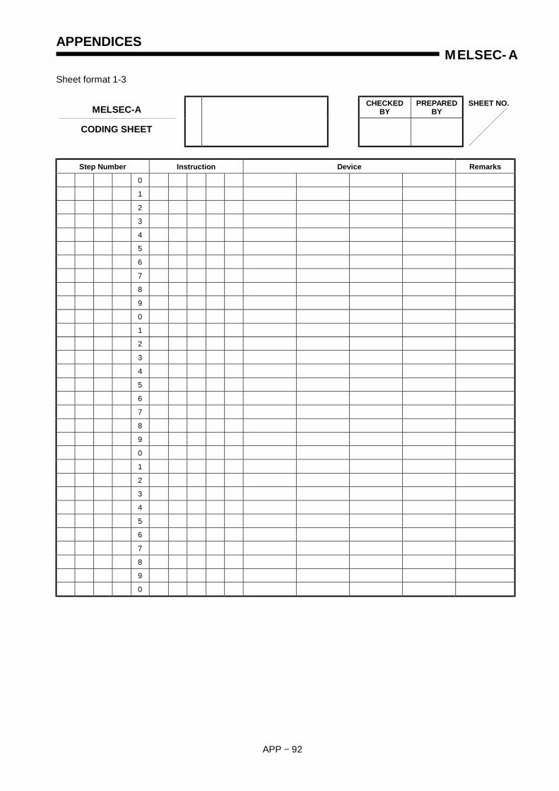
APPENDICES
APP − 92
MELSEC-A
Sheet format 1-3
CHECKEDBY
PREPAREDBY
SHEET NO.
Step Number Instruction Device Remarks
0
1
2
3
4
5
6
7
8
9
0
1
2
3
4
5
6
7
8
9
0
1
2
3
4
5
6
7
8
9
0
MELSEC-A
CODING SHEET

APPENDICES
APP − 93
MELSEC-A
Sheet format 1-4
CHECKEDBY
PREPAREDBY
SHEET NO.
Signal Description Signal Description
0 2
1 3
2 4
3 5
4 6
5 7
6 8
7 9
8 0
9 1
0 2
1 3
2 4
3 5
4 6
5 7
6 8
7 9
8 0
9 1
0 2
1 3
2 4
3 5
4 6
5 7
6 8
7 9
8
9
0
1
MELSEC-A
BIT DEVICE LIST

APPENDICES
APP − 94
MELSEC-A
Sheet format 1-5
CHECKEDBY
PREPAREDBY
SHEET NO.
Data(16 bits/data) Description Data
(16 bits/data) Description
0 0
1 1
2 2
3 3
4 4
5 5
6 6
7 7
8 8
9 9
0 0
1 1
2 2
3 3
4 4
5 5
6 6
7 7
8 8
9 9
MELSEC-A
WORD DEVICE LIST

APPENDICES
APP − 95
MELSEC-A
Sheet format 1-6
CHECKEDBY
PREPAREDBY
SHEET NO.
Failure Type, Condition →→→→ Troubleshooting PointFailureMemoryNumber
External Failure Name
F 0
1
2
3
4
5
6
7
8
9
F 0
1
2
3
4
5
6
7
8
9
F 0
1
2
3
4
5
6
7
8
9
MELSEC-A
ANNUNCIATOR LIST

APPENDICES
APP − 96
MELSEC-A
Sheet format 1-7
CHECKEDBY
PREPAREDBY
SHEET NO.
Number Set Value K Description Application, Operation (Count Input), etc.
0
1
2
3
4
5
6
7
8
9
0
1
2
3
4
5
6
7
8
9
0
1
2
3
4
5
6
7
8
9
MELSEC-A
TIMER, COUNTER LIST

WARRANTY
Please confirm the following product warranty details before starting use.
1. Gratis Warranty Term and Gratis Warranty RangeIf any faults or defects (hereinafter "Failure") found to be the responsibility of Mitsubishi occurs during use of the productwithin the gratis warranty term, the product shall be repaired at no cost via the dealer or Mitsubishi Service Company.Note that if repairs are required at a site overseas, on a detached island or remote place, expenses to dispatch anengineer shall be charged for.[Gratis Warranty Term]
The gratis warranty term of the product shall be for one year after the date of purchase or delivery to a designatedplace.Note that after manufacture and shipment from Mitsubishi, the maximum distribution period shall be six (6) months, andthe longest gratis warranty term after manufacturing shall be eighteen (18) months. The gratis warranty term of repairparts shall not exceed the gratis warranty term before repairs.
[Gratis Warranty Range](1) The range shall be limited to normal use within the usage state, usage methods and usage environment, etc.,
which follow the conditions and precautions, etc., given in the instruction manual, user's manual and caution labelson the product.
(2) Even within the gratis warranty term, repairs shall be charged for in the following cases.1. Failure occurring from inappropriate storage or handling, carelessness or negligence by the user. Failure caused
by the user's hardware or software design.2. Failure caused by unapproved modifications, etc., to the product by the user.3. When the Mitsubishi product is assembled into a user's device, Failure that could have been avoided if functions
or structures, judged as necessary in the legal safety measures the user's device is subject to or as necessaryby industry standards, had been provided.
4. Failure that could have been avoided if consumable parts (battery, backlight, fuse, etc.) designated in theinstruction manual had been correctly serviced or replaced.
5. Failure caused by external irresistible forces such as fires or abnormal voltages, and Failure caused by forcemajeure such as earthquakes, lightning, wind and water damage.
6. Failure caused by reasons unpredictable by scientific technology standards at time of shipment from Mitsubishi.7. Any other failure found not to be the responsibility of Mitsubishi or the user.
2. Onerous repair term after discontinuation of production(1) Mitsubishi shall accept onerous product repairs for seven (7) years after production of the product is discontinued.
Discontinuation of production shall be notified with Mitsubishi Technical Bulletins, etc.(2) Product supply (including repair parts) is not possible after production is discontinued.
3. Overseas serviceOverseas, repairs shall be accepted by Mitsubishi's local overseas FA Center. Note that the repair conditions at each FACenter may differ.
4. Exclusion of chance loss and secondary loss from warranty liabilityRegardless of the gratis warranty term, Mitsubishi shall not be liable for compensation to damages caused by any causefound not to be the responsibility of Mitsubishi, chance losses, lost profits incurred to the user by Failures of Mitsubishiproducts, damages and secondary damages caused from special reasons regardless of Mitsubishi's expectations,compensation for accidents, and compensation for damages to products other than Mitsubishi products and other duties.
5. Changes in product specificationsThe specifications given in the catalogs, manuals or technical documents are subject to change without prior notice.
6. Product application(1) In using the Mitsubishi MELSEC programmable logic controller, the usage conditions shall be that the application will
not lead to a major accident even if any problem or fault should occur in the programmable logic controller device, andthat backup and fail-safe functions are systematically provided outside of the device for any problem or fault.
(2) The Mitsubishi general-purpose programmable logic controller has been designed and manufactured for applicationsin general industries, etc. Thus, applications in which the public could be affected such as in nuclear power plants andother power plants operated by respective power companies, and applications in which a special quality assurancesystem is required, such as for Railway companies or National Defense purposes shall be excluded from theprogrammable logic controller applications.Note that even with these applications, if the user approves that the application is to be limited and a special quality isnot required, application shall be possible.When considering use in aircraft, medical applications, railways, incineration and fuel devices, manned transportdevices, equipment for recreation and amusement, and safety devices, in which human life or assets could be greatlyaffected and for which a particularly high reliability is required in terms of safety and control system, please consultwith Mitsubishi and discuss the required specifications.

Mitsubishi Programmable Logic Controller
Type ACPU/QCPU-A (A Mode)(Common Instructions)
Programming Manual
MODEL
MODELCODE
ACPU-COMMON-P-E
13J741
IB(NA)-66250-H(0312)MEE
Type ACPU/QCPU-A (A Mode)(Common Instructions)
Programming Manual
P
Type A
CP
U/Q
CP
U-A
(A M
ode)(Com
mon Instructions) P
rogramm
ing Manual
Specifications subject to change without notice.
When exported from Japan, this manual does not require application to theMinistry of Economy, Trade and Industry for service transaction permission.
HEAD OFFICE : 1-8-12, OFFICE TOWER Z 14F HARUMI CHUO-KU 104-6212,JAPANNAGOYA WORKS : 1-14 , YADA-MINAMI 5-CHOME , HIGASHI-KU, NAGOYA , JAPAN


![Power supply specifications (The general specifications ...GT10-C30R4-25P Between QnA/ACPU/motion controller CPU (A series)/FXCPU and GOT Between RS-422 conversion cable (FA-CNV[]CBL)](https://static.documents.pub/doc/80x56/5e6f305940141e598a1ef202/power-supply-specifications-the-general-specifications-gt10-c30r4-25p-between.jpg)


