www.ti.com SBFS002B –JULY 1992–REVISED OCTOBER 2010
UNIVERSAL ACTIVE FILTERCheck for Samples: UAF42
1FEATURES DESCRIPTION2• VERSATILE: The UAF42 is a universal active filter that can be
configured for a wide range of low-pass, high-pass,– Low-Pass, High-Passand band-pass filters. It uses a classic state-variable– Band-Pass, Band-Rejectanalog architecture with an inverting amplifier and two
• SIMPLE DESIGN PROCEDURE integrators. The integrators include on-chip 1000pF• ACCURATE FREQUENCY AND Q: capacitors trimmed to 0.5%. This architecture solves
one of the most difficult problems of active filter– Includes On-Chip 1000pF ±0.5% Capacitorsdesign—obtaining tight tolerance, low-loss capacitors.
APPLICATIONS A DOS-compatible filter design program allows easyimplementation of many filter types, such as• TEST EQUIPMENTButterworth, Bessel, and Chebyshev. A fourth,• COMMUNICATIONS EQUIPMENTuncommitted FET-input op amp (identical to the other
• MEDICAL INSTRUMENTATION three) can be used to form additional stages, or for• DATA ACQUISITION SYSTEMS special filters such as band-reject and Inverse
Chebyshev.• MONOLITHIC REPLACEMENT FOR UAF41
The classical topology of the UAF42 forms atime-continuous filter, free from the anomalies andswitching noise associated with switched-capacitorfilter types.
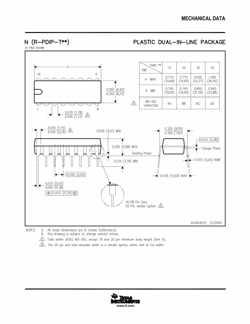
The UAF42 is available in 14-pin plastic DIP andSOIC-16 surface-mount packages, specified for the–25°C to +85°C temperature range.
blank
blank
blank
blank
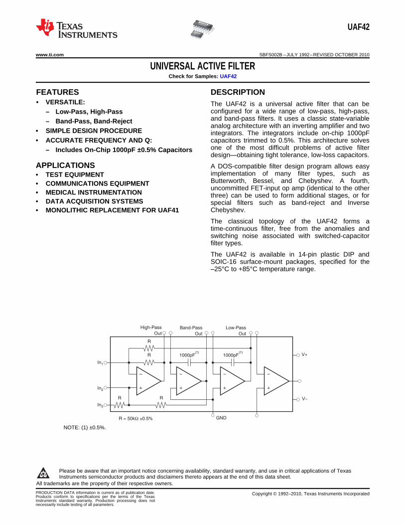
NOTE: (1) ±0.5%.
1
Please be aware that an important notice concerning availability, standard warranty, and use in critical applications of TexasInstruments semiconductor products and disclaimers thereto appears at the end of this data sheet.
2All trademarks are the property of their respective owners.
SBFS002B –JULY 1992–REVISED OCTOBER 2010 www.ti.com
This integrated circuit can be damaged by ESD. Texas Instruments recommends that all integrated circuits be handled withappropriate precautions. Failure to observe proper handling and installation procedures can cause damage.
ESD damage can range from subtle performance degradation to complete device failure. Precision integrated circuits may be moresusceptible to damage because very small parametric changes could cause the device not to meet its published specifications.
ABSOLUTE MAXIMUM RATINGS (1)
Over operating free-air temperature range unless otherwise noted.UAF42 UNIT
Power Supply Voltage ±18 V
Input Voltage ±VS ±0.7 V
Output Short-Circuit Continuous
Operating Temperature –40 to +85 °C
Storage Temperature –40 to +125 °C
Junction Temperature +125 °C
(1) Stresses above these ratings may cause permanent damage. Exposure to absolute maximum conditions for extended period maydegrade device reliability. These are stress ratings only, and functional operation of the device at these or any other conditions beyondthose specified is not supported.
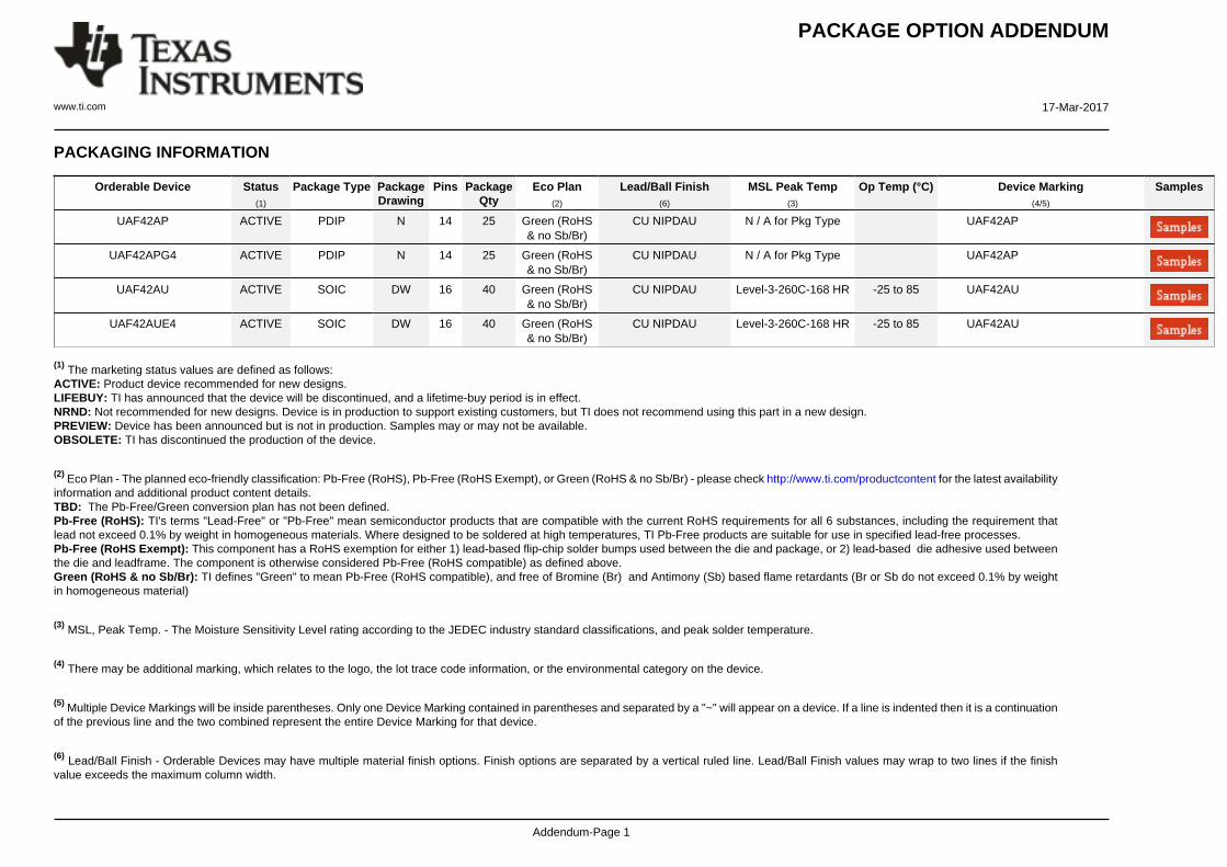
(1) For the most current package and ordering information see the Package Option Addendum at the end of this document, or see the TIweb site at www.ti.com.
PIN CONFIGURATIONS
P PACKAGE U PACKAGEPDIP-14 SOIC-16
(TOP VIEW) (TOP VIEW)
NOTE: (1) NC = no connection. For bestperformance connect all NC pins to groundto minimize inter-lead capacitance.
www.ti.com SBFS002B –JULY 1992–REVISED OCTOBER 2010
APPLICATION INFORMATION
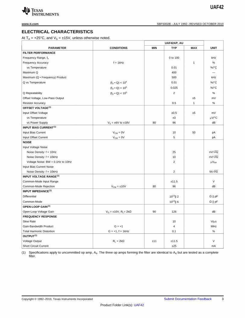
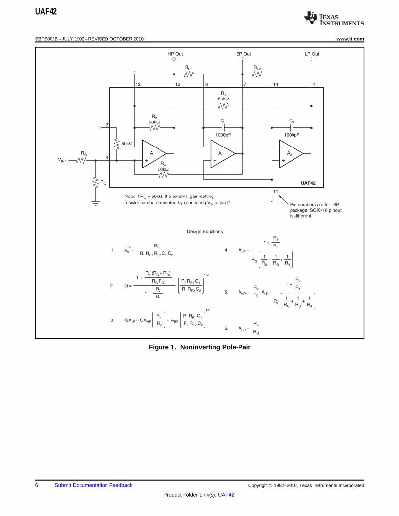
The UAF42 is a monolithic implementation of the The basic building element of the mostproven state-variable analog filter topology. This commonly-used filter types is the second-orderdevice is pin-compatible with the popular UAF41 section. This section provides a complex-conjugateanalog filter, and it provides several improvements. pair of poles. The natural frequency, wn, and Q of the
pole pair determine the characteristic response of theThe slew rate of the UAF42 has been increased to section. The low-pass transfer function is shown in10V/ms, versus 1.6V/ms for the UAF41. Equation 1:Frequency • Q product of the UAF42 has beenimproved, and the useful natural frequency extendedby a factor of four to 100kHz. FET input op amps on (1)the UAF42 provide very low input bias current. Themonolithic construction of the UAF42 provides lower The high-pass transfer function is given bycost and improved reliability. Equation 2:
DESIGN PROGRAM(2)
Application report SBFA002 (available for downloadThe band-pass transfer function is calculated usingat www.ti.com) and a computer-aided design programEquation 3:also available from Texas Instruments, make it easy
to design and implement many kinds of active filters.The DOS-compatible program guides you through the
(3)design process and automatically calculatescomponent values. A band-reject response is obtained by summing the
low-pass and high-pass outputs, yielding the transferLow-pass, high-pass, band-pass and band-rejectfunction shown in Equation 4:(notch) filters can be designed. The program supports
the three most commonly-used all-pole filter types:Butterworth, Chebyshev and Bessel. The less-familiar
(4)inverse Chebyshev is also supported, providing asmooth passband response with ripple in the stop The most common filter types are formed with one orband. more cascaded second-order sections. Each section
is designed for wn and Q according to the filter typeWith each data entry, the program automatically(Butterworth, Bessel, Chebyshev, etc.) and cutoffcalculates and displays filter performance. Thisfrequency. While tabulated data can be found infeature allows a spreadsheet-like what-if designvirtually any filter design text, the design programapproach. For example, a user can quickly determine,eliminates this tedious procedure.by trial and error, how many poles are required for a
desired attenuation in the stopband. Gain/phase plots Second-order sections may be noninvertingmay be viewed for any response type. (Figure 1) or inverting (Figure 2). Design equations
for these two basic configurations are shown forreference. The design program solves theseequations, providing complete results, includingcomponent values.
UAF42AP ACTIVE PDIP N 14 25 Green (RoHS& no Sb/Br)
CU NIPDAU N / A for Pkg Type UAF42AP
UAF42APG4 ACTIVE PDIP N 14 25 Green (RoHS& no Sb/Br)
CU NIPDAU N / A for Pkg Type UAF42AP
UAF42AU ACTIVE SOIC DW 16 40 Green (RoHS& no Sb/Br)
CU NIPDAU Level-3-260C-168 HR -25 to 85 UAF42AU
UAF42AUE4 ACTIVE SOIC DW 16 40 Green (RoHS& no Sb/Br)
CU NIPDAU Level-3-260C-168 HR -25 to 85 UAF42AU
(1) The marketing status values are defined as follows:ACTIVE: Product device recommended for new designs.LIFEBUY: TI has announced that the device will be discontinued, and a lifetime-buy period is in effect.NRND: Not recommended for new designs. Device is in production to support existing customers, but TI does not recommend using this part in a new design.PREVIEW: Device has been announced but is not in production. Samples may or may not be available.OBSOLETE: TI has discontinued the production of the device.
(2) Eco Plan - The planned eco-friendly classification: Pb-Free (RoHS), Pb-Free (RoHS Exempt), or Green (RoHS & no Sb/Br) - please check http://www.ti.com/productcontent for the latest availabilityinformation and additional product content details.TBD: The Pb-Free/Green conversion plan has not been defined.Pb-Free (RoHS): TI's terms "Lead-Free" or "Pb-Free" mean semiconductor products that are compatible with the current RoHS requirements for all 6 substances, including the requirement thatlead not exceed 0.1% by weight in homogeneous materials. Where designed to be soldered at high temperatures, TI Pb-Free products are suitable for use in specified lead-free processes.Pb-Free (RoHS Exempt): This component has a RoHS exemption for either 1) lead-based flip-chip solder bumps used between the die and package, or 2) lead-based die adhesive used betweenthe die and leadframe. The component is otherwise considered Pb-Free (RoHS compatible) as defined above.Green (RoHS & no Sb/Br): TI defines "Green" to mean Pb-Free (RoHS compatible), and free of Bromine (Br) and Antimony (Sb) based flame retardants (Br or Sb do not exceed 0.1% by weightin homogeneous material)
(3) MSL, Peak Temp. - The Moisture Sensitivity Level rating according to the JEDEC industry standard classifications, and peak solder temperature.
(4) There may be additional marking, which relates to the logo, the lot trace code information, or the environmental category on the device.
(5) Multiple Device Markings will be inside parentheses. Only one Device Marking contained in parentheses and separated by a "~" will appear on a device. If a line is indented then it is a continuationof the previous line and the two combined represent the entire Device Marking for that device.
(6) Lead/Ball Finish - Orderable Devices may have multiple material finish options. Finish options are separated by a vertical ruled line. Lead/Ball Finish values may wrap to two lines if the finishvalue exceeds the maximum column width.
Important Information and Disclaimer:The information provided on this page represents TI's knowledge and belief as of the date that it is provided. TI bases its knowledge and belief on informationprovided by third parties, and makes no representation or warranty as to the accuracy of such information. Efforts are underway to better integrate information from third parties. TI has taken andcontinues to take reasonable steps to provide representative and accurate information but may not have conducted destructive testing or chemical analysis on incoming materials and chemicals.TI and TI suppliers consider certain information to be proprietary, and thus CAS numbers and other limited information may not be available for release.
In no event shall TI's liability arising out of such information exceed the total purchase price of the TI part(s) at issue in this document sold by TI to Customer on an annual basis.
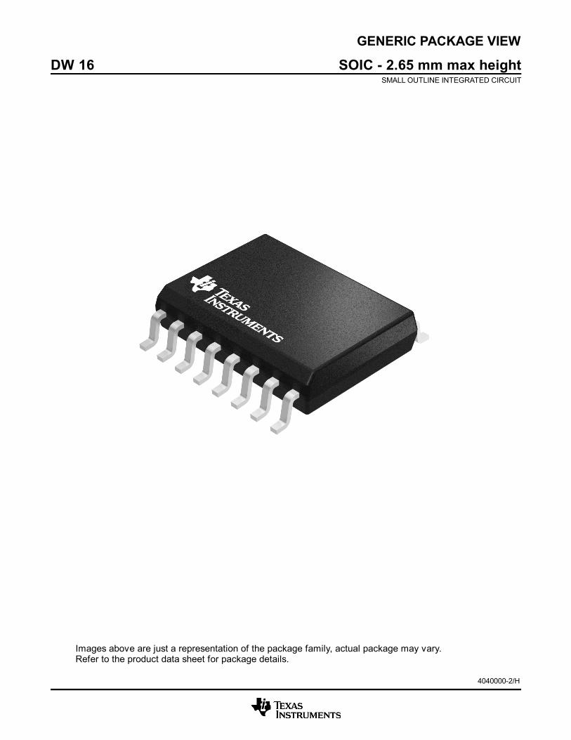
GENERIC PACKAGE VIEW
Images above are just a representation of the package family, actual package may vary.Refer to the product data sheet for package details.
DW 16 SOIC - 2.65 mm max heightSMALL OUTLINE INTEGRATED CIRCUIT
4040000-2/H
www.ti.com
PACKAGE OUTLINE
C
TYP10.639.97
2.65 MAX
14X 1.27
16X 0.510.31
2X8.89
TYP0.330.10
0 - 80.30.1
(1.4)
0.25GAGE PLANE
1.270.40
A
NOTE 3
10.510.1
BNOTE 4
7.67.4
4220721/A 07/2016
SOIC - 2.65 mm max heightDW0016ASOIC
NOTES: 1. All linear dimensions are in millimeters. Dimensions in parenthesis are for reference only. Dimensioning and tolerancing per ASME Y14.5M. 2. This drawing is subject to change without notice. 3. This dimension does not include mold flash, protrusions, or gate burrs. Mold flash, protrusions, or gate burrs shall not exceed 0.15 mm, per side. 4. This dimension does not include interlead flash. Interlead flash shall not exceed 0.25 mm, per side.5. Reference JEDEC registration MS-013.
1 16
0.25 C A B
98
PIN 1 IDAREA
SEATING PLANE
0.1 C
SEE DETAIL A
DETAIL ATYPICAL
SCALE 1.500
www.ti.com
EXAMPLE BOARD LAYOUT
0.07 MAXALL AROUND
0.07 MINALL AROUND
(9.3)
14X (1.27)
R0.05 TYP
16X (2)
16X (0.6)
4220721/A 07/2016
SOIC - 2.65 mm max heightDW0016ASOIC
NOTES: (continued) 6. Publication IPC-7351 may have alternate designs. 7. Solder mask tolerances between and around signal pads can vary based on board fabrication site.
METAL SOLDER MASKOPENING
NON SOLDER MASKDEFINED
SOLDER MASK DETAILS
OPENINGSOLDER MASK METAL
SOLDER MASKDEFINED
LAND PATTERN EXAMPLESCALE:7X
SYMM
1
8 9
16
SEEDETAILS
SYMM
www.ti.com
EXAMPLE STENCIL DESIGN
R0.05 TYP
16X (2)
16X (0.6)
14X (1.27)
(9.3)
4220721/A 07/2016
SOIC - 2.65 mm max heightDW0016ASOIC
NOTES: (continued) 8. Laser cutting apertures with trapezoidal walls and rounded corners may offer better paste release. IPC-7525 may have alternate design recommendations. 9. Board assembly site may have different recommendations for stencil design.
SOLDER PASTE EXAMPLEBASED ON 0.125 mm THICK STENCIL
SCALE:7X
SYMM
SYMM
1
8 9
16
IMPORTANT NOTICE
Texas Instruments Incorporated (TI) reserves the right to make corrections, enhancements, improvements and other changes to itssemiconductor products and services per JESD46, latest issue, and to discontinue any product or service per JESD48, latest issue. Buyersshould obtain the latest relevant information before placing orders and should verify that such information is current and complete.TI’s published terms of sale for semiconductor products (http://www.ti.com/sc/docs/stdterms.htm) apply to the sale of packaged integratedcircuit products that TI has qualified and released to market. Additional terms may apply to the use or sale of other types of TI products andservices.Reproduction of significant portions of TI information in TI data sheets is permissible only if reproduction is without alteration and isaccompanied by all associated warranties, conditions, limitations, and notices. TI is not responsible or liable for such reproduceddocumentation. Information of third parties may be subject to additional restrictions. Resale of TI products or services with statementsdifferent from or beyond the parameters stated by TI for that product or service voids all express and any implied warranties for theassociated TI product or service and is an unfair and deceptive business practice. TI is not responsible or liable for any such statements.Buyers and others who are developing systems that incorporate TI products (collectively, “Designers”) understand and agree that Designersremain responsible for using their independent analysis, evaluation and judgment in designing their applications and that Designers havefull and exclusive responsibility to assure the safety of Designers' applications and compliance of their applications (and of all TI productsused in or for Designers’ applications) with all applicable regulations, laws and other applicable requirements. Designer represents that, withrespect to their applications, Designer has all the necessary expertise to create and implement safeguards that (1) anticipate dangerousconsequences of failures, (2) monitor failures and their consequences, and (3) lessen the likelihood of failures that might cause harm andtake appropriate actions. Designer agrees that prior to using or distributing any applications that include TI products, Designer willthoroughly test such applications and the functionality of such TI products as used in such applications.TI’s provision of technical, application or other design advice, quality characterization, reliability data or other services or information,including, but not limited to, reference designs and materials relating to evaluation modules, (collectively, “TI Resources”) are intended toassist designers who are developing applications that incorporate TI products; by downloading, accessing or using TI Resources in anyway, Designer (individually or, if Designer is acting on behalf of a company, Designer’s company) agrees to use any particular TI Resourcesolely for this purpose and subject to the terms of this Notice.TI’s provision of TI Resources does not expand or otherwise alter TI’s applicable published warranties or warranty disclaimers for TIproducts, and no additional obligations or liabilities arise from TI providing such TI Resources. TI reserves the right to make corrections,enhancements, improvements and other changes to its TI Resources. TI has not conducted any testing other than that specificallydescribed in the published documentation for a particular TI Resource.Designer is authorized to use, copy and modify any individual TI Resource only in connection with the development of applications thatinclude the TI product(s) identified in such TI Resource. NO OTHER LICENSE, EXPRESS OR IMPLIED, BY ESTOPPEL OR OTHERWISETO ANY OTHER TI INTELLECTUAL PROPERTY RIGHT, AND NO LICENSE TO ANY TECHNOLOGY OR INTELLECTUAL PROPERTYRIGHT OF TI OR ANY THIRD PARTY IS GRANTED HEREIN, including but not limited to any patent right, copyright, mask work right, orother intellectual property right relating to any combination, machine, or process in which TI products or services are used. Informationregarding or referencing third-party products or services does not constitute a license to use such products or services, or a warranty orendorsement thereof. Use of TI Resources may require a license from a third party under the patents or other intellectual property of thethird party, or a license from TI under the patents or other intellectual property of TI.TI RESOURCES ARE PROVIDED “AS IS” AND WITH ALL FAULTS. TI DISCLAIMS ALL OTHER WARRANTIES ORREPRESENTATIONS, EXPRESS OR IMPLIED, REGARDING RESOURCES OR USE THEREOF, INCLUDING BUT NOT LIMITED TOACCURACY OR COMPLETENESS, TITLE, ANY EPIDEMIC FAILURE WARRANTY AND ANY IMPLIED WARRANTIES OFMERCHANTABILITY, FITNESS FOR A PARTICULAR PURPOSE, AND NON-INFRINGEMENT OF ANY THIRD PARTY INTELLECTUALPROPERTY RIGHTS. TI SHALL NOT BE LIABLE FOR AND SHALL NOT DEFEND OR INDEMNIFY DESIGNER AGAINST ANY CLAIM,INCLUDING BUT NOT LIMITED TO ANY INFRINGEMENT CLAIM THAT RELATES TO OR IS BASED ON ANY COMBINATION OFPRODUCTS EVEN IF DESCRIBED IN TI RESOURCES OR OTHERWISE. IN NO EVENT SHALL TI BE LIABLE FOR ANY ACTUAL,DIRECT, SPECIAL, COLLATERAL, INDIRECT, PUNITIVE, INCIDENTAL, CONSEQUENTIAL OR EXEMPLARY DAMAGES INCONNECTION WITH OR ARISING OUT OF TI RESOURCES OR USE THEREOF, AND REGARDLESS OF WHETHER TI HAS BEENADVISED OF THE POSSIBILITY OF SUCH DAMAGES.Unless TI has explicitly designated an individual product as meeting the requirements of a particular industry standard (e.g., ISO/TS 16949and ISO 26262), TI is not responsible for any failure to meet such industry standard requirements.Where TI specifically promotes products as facilitating functional safety or as compliant with industry functional safety standards, suchproducts are intended to help enable customers to design and create their own applications that meet applicable functional safety standardsand requirements. Using products in an application does not by itself establish any safety features in the application. Designers mustensure compliance with safety-related requirements and standards applicable to their applications. Designer may not use any TI products inlife-critical medical equipment unless authorized officers of the parties have executed a special contract specifically governing such use.Life-critical medical equipment is medical equipment where failure of such equipment would cause serious bodily injury or death (e.g., lifesupport, pacemakers, defibrillators, heart pumps, neurostimulators, and implantables). Such equipment includes, without limitation, allmedical devices identified by the U.S. Food and Drug Administration as Class III devices and equivalent classifications outside the U.S.TI may expressly designate certain products as completing a particular qualification (e.g., Q100, Military Grade, or Enhanced Product).Designers agree that it has the necessary expertise to select the product with the appropriate qualification designation for their applicationsand that proper product selection is at Designers’ own risk. Designers are solely responsible for compliance with all legal and regulatoryrequirements in connection with such selection.Designer will fully indemnify TI and its representatives against any damages, costs, losses, and/or liabilities arising out of Designer’s non-compliance with the terms and provisions of this Notice.