An IMPORTANT NOTICE at the end of this data sheet addresses availability, warranty, changes, use in safety-critical applications,intellectual property matters and other important disclaimers. PRODUCTION DATA.
UCC21520, UCC21520ASLUSCJ9C –JUNE 2016–REVISED DECEMBER 2017
1 Features1• Universal: Dual Low-Side, Dual High-Side or Half-
Bridge Driver• Operating Temperature Range –40 to +125°C• Switching Parameters:
– 19-ns Typical Propagation Delay– 10-ns Minimum Pulse Width– 5-ns Maximum Delay Matching– 5-ns Maximum Pulse-Width Distortion
• Common-Mode Transient Immunity (CMTI)Greater than 100 V/ns
• Surge Immunity up to 12.8 kV• Isolation Barrier Life >40 Years• 4-A Peak Source, 6-A Peak Sink Output• TTL and CMOS Compatible Inputs• 3-V to 18-V Input VCCI Range to Interface with
Both Digital and Analog Controllers• Up to 25-V VDD Output Drive Supply
– 5-V and 8-V VDD UVLO Options• Programmable Overlap and Dead Time• Rejects Input Pulses and Noise Transients
Shorter than 5 ns• Fast Disable for Power Sequencing• Industry Standard Wide Body SOIC-16 (DW)
Package• Safety-Related Certifications:
– 8000-VPK Reinforced Isolation per DIN V VDEV 0884-11:2017-01
– 5.7-kVRMS Isolation for 1 Minute per UL 1577– CSA Certification per IEC 60950-1, IEC 62368-
1, IEC 61010-1 and IEC 60601-1 EndEquipment Standards
– CQC Certification per GB4943.1-2011
2 Applications• HEV and BEV Battery Chargers• Isolated Converters in DC-DC and AC-DC Power
Supplies• Server, Telecom, IT and Industrial Infrastructures• Motor Drive and DC-to-AC Solar Inverters• LED Lighting• Inductive Heating• Uninterruptible Power Supply (UPS)
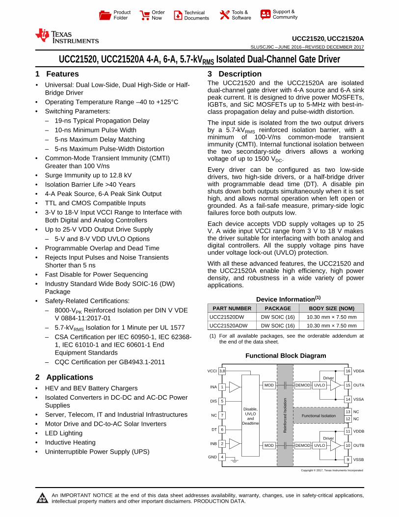
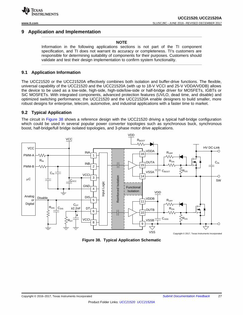
3 DescriptionThe UCC21520 and the UCC21520A are isolateddual-channel gate driver with 4-A source and 6-A sinkpeak current. It is designed to drive power MOSFETs,IGBTs, and SiC MOSFETs up to 5-MHz with best-in-class propagation delay and pulse-width distortion.
The input side is isolated from the two output driversby a 5.7-kVRMS reinforced isolation barrier, with aminimum of 100-V/ns common-mode transientimmunity (CMTI). Internal functional isolation betweenthe two secondary-side drivers allows a workingvoltage of up to 1500 VDC.
Every driver can be configured as two low-sidedrivers, two high-side drivers, or a half-bridge driverwith programmable dead time (DT). A disable pinshuts down both outputs simultaneously when it is sethigh, and allows normal operation when left open orgrounded. As a fail-safe measure, primary-side logicfailures force both outputs low.
Each device accepts VDD supply voltages up to 25V. A wide input VCCI range from 3 V to 18 V makesthe driver suitable for interfacing with both analog anddigital controllers. All the supply voltage pins haveunder voltage lock-out (UVLO) protection.
With all these advanced features, the UCC21520 andthe UCC21520A enable high efficiency, high powerdensity, and robustness in a wide variety of powerapplications.
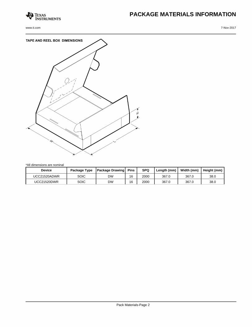
Device Information(1)
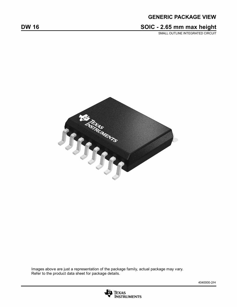
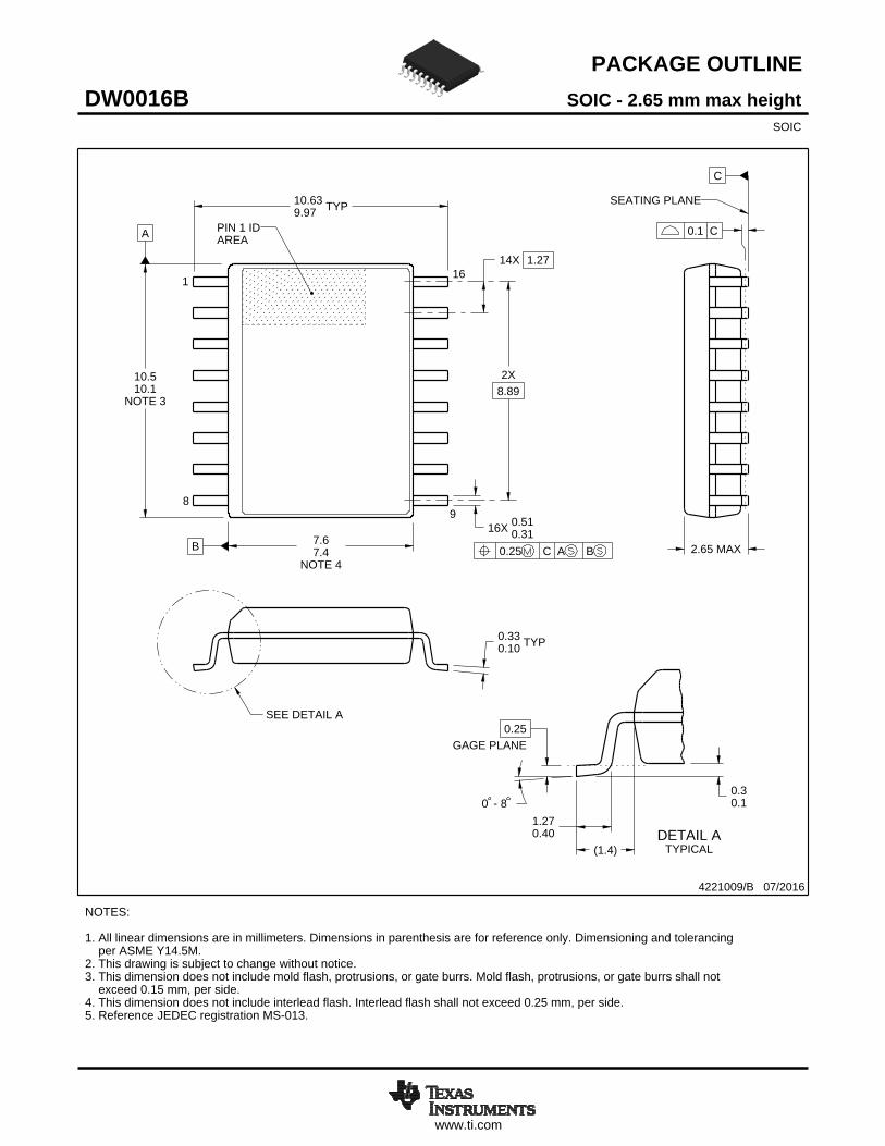
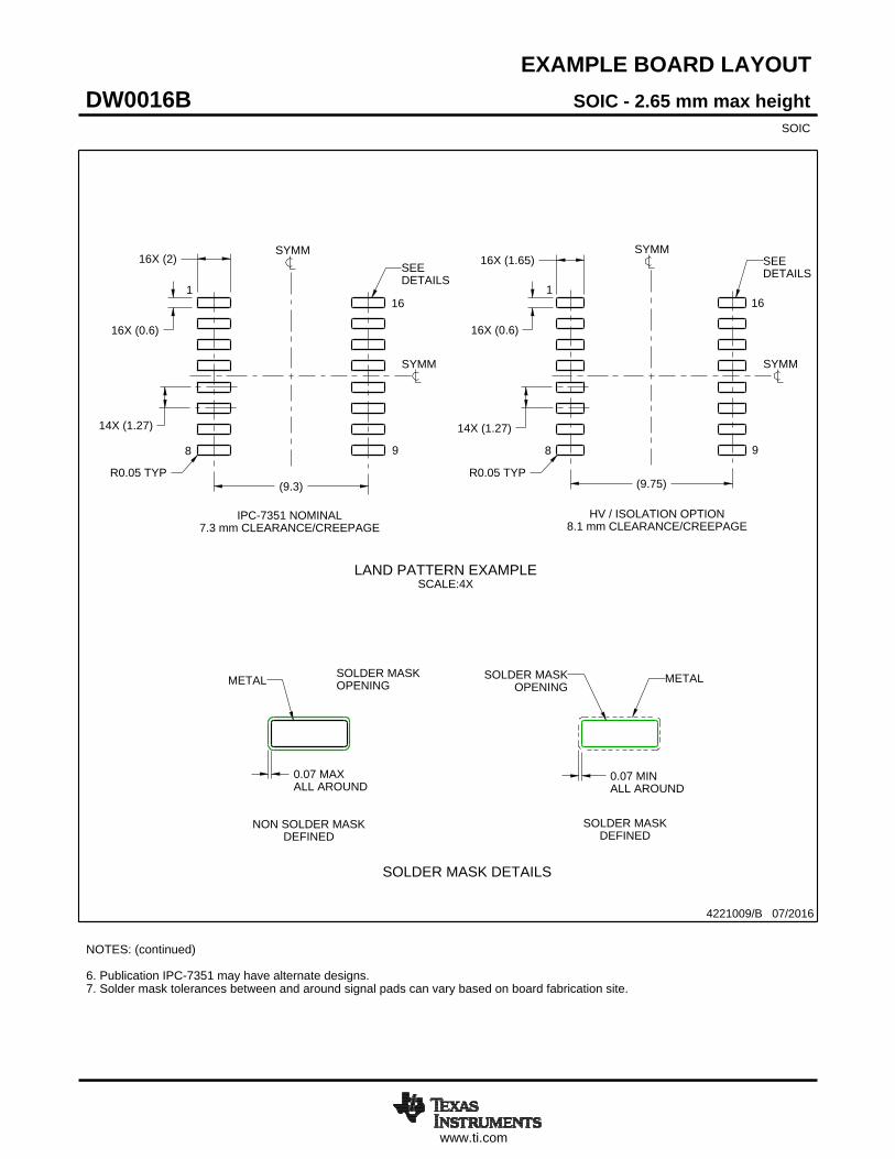
PART NUMBER PACKAGE BODY SIZE (NOM)UCC21520DW DW SOIC (16) 10.30 mm × 7.50 mmUCC21520ADW DW SOIC (16) 10.30 mm × 7.50 mm
(1) For all available packages, see the orderable addendum atthe end of the data sheet.
7 Parameter Measurement Information ................ 167.1 Propagation Delay and Pulse Width Distortion....... 167.2 Rising and Falling Time ......................................... 167.3 Input and Disable Response Time.......................... 167.4 Programable Dead Time ........................................ 17
7.5 Power-up UVLO Delay to OUTPUT........................ 177.6 CMTI Testing........................................................... 18
10 Power Supply Recommendations ..................... 3811 Layout................................................................... 39
11.1 Layout Guidelines ................................................. 3911.2 Layout Example .................................................... 40
12 Device and Documentation Support ................. 4212.1 Documentation Support ....................................... 4212.2 Certifications ......................................................... 4212.3 Receiving Notification of Documentation Updates 4212.4 Community Resources.......................................... 4212.5 Trademarks ........................................................... 4212.6 Electrostatic Discharge Caution............................ 4212.7 Glossary ................................................................ 42
13 Mechanical, Packaging, and OrderableInformation ........................................................... 42
4 Revision History
Changes from Revision B (November 2016) to Revision C Page
• Changed VDE and CSA safety-related certification descriptions in features section ............................................................ 1• Added "UCC21520A" in the title ............................................................................................................................................. 1• Added detailed description for DISABLE Pin and DT Pin ...................................................................................................... 4• Changed thermal matrix in thermal information table............................................................................................................. 6• Changed table note #2 in the insulation specifications table ................................................................................................. 7• Changed from VDE V 0884-10 to VDE V 0884-11 in insulation specification and safety-related certification table ............. 8• Added CSA master contract number, and related notes in CSA column of safety-related certification table........................ 8• Changed maximum working voltage from 400-VRMS to 660-VRMS in CQC column of safety-related certification table ......... 8• Changed testing conditions of RθJA to match thermal matrix table......................................................................................... 8• Changed the safety output supply current and power to correspond the RθJA update........................................................... 8• Changed table note to explain how safety-limiting values are calculated .............................................................................. 8• Changed UCC21520ADW and UCC21520DW UVLO threshold specifications..................................................................... 9• Added minimum propagation delay for tPDHL and tPDLH ........................................................................................................ 10• Added |CMH| and |CML| to CMTI specification ..................................................................................................................... 10• Added typical curves of 5-V UVLO hysteresis and ON-OFF thresholds .............................................................................. 13• Added feature descriptions for UVLO delay to OUTPUT .................................................................................................... 17• Changed equation (14) and (15) in the section of estimating the driver power loss............................................................ 31• Changed junction temperature estimation with improved method for customer systems.................................................... 31• Added bullet "It is recommended..." bullet to the component placement in the Layout Guidelines. ................................... 39• Added more thermal improvement details in the section of layout guidelines ..................................................................... 39• Added CSA online certification directory to the certification section ................................................................................... 42
Changes from Revision A (June 2016) to Revision B Page
• Changed UVLO options from 5 V, 8 V and 12 V to 5 V and 8 V. ......................................................................................... 1• Changed planned CQC Certification per GB4943.1-2011 certification to completed. .......................................................... 1• Changed DT pin description. .................................................................................................................................................. 4• Changed input signal voltage Max rating in two places from VVCCI to VVCCI+0.3. .................................................................. 5• Deleted Driver output bias supply 12-V option. ...................................................................................................................... 5• Added 400-VRMS maximum working voltage. ......................................................................................................................... 8• Changed VDE certification from "Agency Qualification Planned" to "Certification number: 40040142". ............................... 8• Added Certification number: CQC16001155011. ................................................................................................................... 8• Changed 5-V UVLO Version title to UCC21520ADW UVLO THRESHOLDS (5-V UVLO Version)....................................... 9• Changed 8-V UVLO Version title to UCC21520DW UVLO THRESHOLDS (8-V UVLO Version). ........................................ 9• Deleted 12-V UVLO VERSION. ............................................................................................................................................. 9• Added OUTA to Dead-Time Switching Parameters. ........................................................................................................... 17• Changed the Functional Block Diagram. ............................................................................................................................. 19• Changed ESD Structure image. .......................................................................................................................................... 24• Added "The steady state voltage at DT pin" paragraph to the "DT Pin Left Open or Connected to a Programming
Resistor between DT and GND Pins" section. .................................................................................................................... 25• Changed Input and Output Logic Relationship With Input Signals graph to include dead time (DT). ................................. 25• Added RGS resister off of pin 9/10. .................................................................................................................................... 27• Changed Typical Application Schematic to included the 2.2-nF capacitor. ........................................................................ 27• Added "It is recommended..." sentence to the Dead Time Setting Guidelines section. ...................................................... 33• Added bullet "It is recommended..." bullet to the component placement in the Layout Guidelines. .................................... 39• Changed all images in the Layout Example section. .......................................................................................................... 40• Added VDE certification........................................................................................................................................................ 42• Added CQC online certification directory to the certification section. .................................................................................. 42
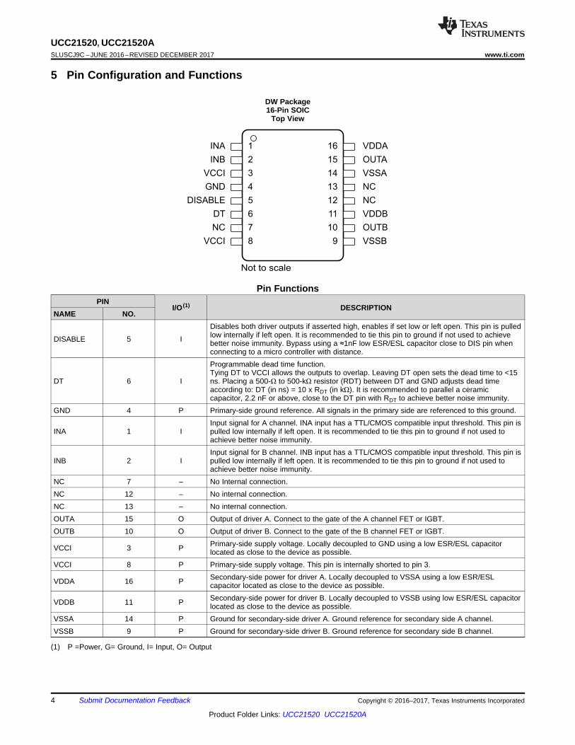
Disables both driver outputs if asserted high, enables if set low or left open. This pin is pulledlow internally if left open. It is recommended to tie this pin to ground if not used to achievebetter noise immunity. Bypass using a ≈1nF low ESR/ESL capacitor close to DIS pin whenconnecting to a micro controller with distance.
DT 6 I
Programmable dead time function.Tying DT to VCCI allows the outputs to overlap. Leaving DT open sets the dead time to <15ns. Placing a 500-Ω to 500-kΩ resistor (RDT) between DT and GND adjusts dead timeaccording to: DT (in ns) = 10 x RDT (in kΩ). It is recommended to parallel a ceramiccapacitor, 2.2 nF or above, close to the DT pin with RDT to achieve better noise immunity.
GND 4 P Primary-side ground reference. All signals in the primary side are referenced to this ground.
INA 1 IInput signal for A channel. INA input has a TTL/CMOS compatible input threshold. This pin ispulled low internally if left open. It is recommended to tie this pin to ground if not used toachieve better noise immunity.
INB 2 IInput signal for B channel. INB input has a TTL/CMOS compatible input threshold. This pin ispulled low internally if left open. It is recommended to tie this pin to ground if not used toachieve better noise immunity.
NC 7 – No Internal connection.NC 12 – No internal connection.NC 13 – No internal connection.OUTA 15 O Output of driver A. Connect to the gate of the A channel FET or IGBT.OUTB 10 O Output of driver B. Connect to the gate of the B channel FET or IGBT.
VCCI 3 P Primary-side supply voltage. Locally decoupled to GND using a low ESR/ESL capacitorlocated as close to the device as possible.
VCCI 8 P Primary-side supply voltage. This pin is internally shorted to pin 3.
VDDA 16 P Secondary-side power for driver A. Locally decoupled to VSSA using a low ESR/ESLcapacitor located as close to the device as possible.
VDDB 11 P Secondary-side power for driver B. Locally decoupled to VSSB using low ESR/ESL capacitorlocated as close to the device as possible.
VSSA 14 P Ground for secondary-side driver A. Ground reference for secondary side A channel.VSSB 9 P Ground for secondary-side driver B. Ground reference for secondary side B channel.
(1) Stresses beyond those listed under Absolute Maximum Ratings may cause permanent damage to the device. These are stress ratingsonly, which do not imply functional operation of the device at these or any other conditions beyond those indicated under RecommendedOperating Conditions. Exposure to absolute-maximum-rated conditions for extended periods may affect device reliability.
(2) To maintain the recommended operating conditions for TJ, see the Thermal Information.
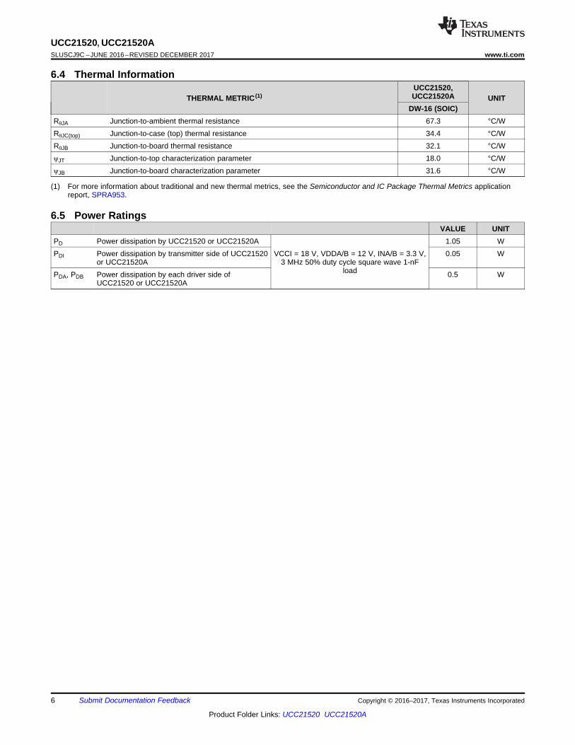
6 Specifications
6.1 Absolute Maximum Ratingsover operating free-air temperature range (unless otherwise noted) (1)
MIN MAX UNITInput bias pin supply voltage VCCI to GND –0.3 20 VDriver bias supply VDDA-VSSA, VDDB-VSSB –0.3 30 V
Output signal voltageOUTA to VSSA, OUTB to VSSB –0.3 VVDDA+0.3,
VVDDB+0.3 V
OUTA to VSSA, OUTB to VSSB,Transient for 200 ns –2 VVDDA+0.3,
VVDDB+0.3 V
Input signal voltageINA, INB, DIS, DT to GND –0.3 VVCCI+0.3 VINA, INB Transient for 50ns –5 VVCCI+0.3 V
Channel to channel voltage VSSA-VSSB, VSSB-VSSA 1500 VJunction temperature, TJ
(2) –40 150 °CStorage temperature, Tstg –65 150 °C
(1) JEDEC document JEP155 states that 500-V HBM allows safe manufacturing with a standard ESD control process.(2) JEDEC document JEP157 states that 250-V CDM allows safe manufacturing with a standard ESD control process.
6.2 ESD RatingsVALUE UNIT
V(ESD) Electrostatic dischargeHuman-body model (HBM), per ANSI/ESDA/JEDEC JS-001 (1) ±4000
VCharged-device model (CDM), per JEDEC specification JESD22-C101 (2) ±1500
6.3 Recommended Operating ConditionsOver operating free-air temperature range (unless otherwise noted)
MIN MAX UNITVCCI VCCI Input supply voltage 3 18 VVDDA,VDDB Driver output bias supply UCC21520ADW – 5-V UVLO version 6.5 25 V
VDDA,VDDB Driver output bias supply UCC21520DW – 8-V UVLO version 9.2 25 V
TA Ambient Temperature –40 125 °CTJ Junction Temperature –40 130 °C
(1) Creepage and clearance requirements should be applied according to the specific equipment isolation standards of an application. Careshould be taken to maintain the creepage and clearance distance of a board design to ensure that the mounting pads of the isolator onthe printed-circuit board do not reduce this distance. Creepage and clearance on a printed-circuit board become equal in certain cases.Techniques such as inserting grooves and/or ribs on a printed circuit board are used to help increase these specifications.
(2) This coupler is suitable for safe electrical insulation only within the safety ratings. Compliance with the safety ratings shall be ensured bymeans of suitable protective circuits.
(3) Testing is carried out in air or oil to determine the intrinsic surge immunity of the isolation barrier.(4) Apparent charge is electrical discharge caused by a partial discharge (pd).(5) All pins on each side of the barrier tied together creating a two-pin device.
6.6 Insulation SpecificationsPARAMETER TEST CONDITIONS VALUE UNIT
CLR External clearance (1) Shortest pin-to-pin distance through air > 8 mmCPG External creepage (1) Shortest pin-to-pin distance across the package surface > 8 mm
DTI Distance through insulation Minimum internal gap (internal clearance) of the doubleinsulation (2 × 10.5 µm) >21 µm
CTI Comparative tracking index DIN EN 60112 (VDE 0303-11); IEC 60112 > 600 VMaterial group According to IEC 60664-1 I
Overvoltage category perIEC 60664-1
Rated mains voltage ≤ 600 VRMS I-IVRated mains voltage ≤ 1000 VRMS I-III
DIN V VDE V 0884-11 (VDE V 0884-11): 2017-01 (2)
VIORMMaximum repetitive peakisolation voltage AC voltage (bipolar) 2121 VPK
VIOWMMaximum working isolationvoltage
AC voltage (sine wave); time dependent dielectric breakdown(TDDB), test (See Figure 1) 1500 VRMS
DC voltage 2121 VDC
VIOTMMaximum transient isolationvoltage
VTEST = VIOTM, t = 60 sec (qualification)VTEST = 1.2 × VIOTM, t = 1 s (100% production) 8000 VPK
VIOSMMaximum surge isolationvoltage (3)
Test method per IEC 62368-1, 1.2/50 µs waveform,VTEST = 1.6 × VIOSM = 12800 VPK (qualification) 8000 VPK
qpd Apparent charge (4)
Method a, After Input/Output safety test subgroup 2/3.Vini = VIOTM, tini = 60s;Vpd(m) = 1.2 X VIORM = 2545 VPK, tm = 10s
<5
pC
Method a, After environmental tests subgroup 1.Vini = VIOTM, tini = 60s;Vpd(m) = 1.6 X VIORM = 3394 VPK, tm = 10s
<5
Method b1; At routine test (100% production) andpreconditioning (type test)Vini = 1.2 × VIOTM; tini = 1s;Vpd(m) = 1.875 * VIORM = 3977 VPK , tm = 1s
<5
CIOBarrier capacitance, input tooutput (5) VIO = 0.4 sin (2πft), f =1 MHz 1.2 pF
RIOIsolation resistance, input tooutput (5)
VIO = 500 V at TA = 25°C > 1012
ΩVIO = 500 V at 100°C ≤ TA ≤ 125°C > 1011
VIO = 500 V at TS =150°C > 109
Pollution degree 2Climatic category 40/125/21
UL 1577
VISO Withstand isolation voltageVTEST = VISO = 5700 VRMS, t = 60 sec. (qualification),VTEST = 1.2 × VISO = 6840VRMS, t = 1 sec (100% production)
Reinforced insulation per CSA 60950-1-07+A1+A2 and IEC 60950-1 2ndEd.+A1+A2, 800 VRMS maximum workingvoltage (pollution degree 2, material group I)Reinforced insulation per CSA 62368-1-14and IEC 62368-1 2nd Ed., 800 VRMSmaximum working voltage (pollution degree2, material group I);Basic insulation per CSA 61010-1-12+A1and IEC 61010-1 3rd Ed., 600 VRMSmaximum working voltage (pollution degree2, material group III);2 MOPP (Means of Patient Protection) perCSA 60601- 1:14 and IEC 60601-1Ed.3+A1, 250 VRMS maximum workingvoltage
Single protection, 5700VRMS
Reinforced Insulation,Altitude ≤ 5000 m,Tropical Climate 660 VRMSmaximum working voltage
(1) The maximum safety temperature, TS, has the same value as the maximum junction temperature, TJ, specified for the device. The ISand PS parameters represent the safety current and safety power respectively. The maximum limits of IS and PS should not beexceeded. These limits vary with the ambient temperature, TA.
The junction-to-air thermal resistance, RθJA, in the Thermal Information table is that of a device installed on a high-K test board forleaded surface-mount packages. Use these equations to calculate the value for each parameter:
TJ = TA + RθJA × P, where P is the power dissipated in the device.
TJ(max) = TS = TA + RθJA × PS, where TJ(max) is the maximum allowed junction temperature.
PS = IS × VI, where VI is the maximum input voltage.
6.8 Safety-Limiting ValuesSafety limiting intends to minimize potential damage to the isolation barrier upon failure of input or output circuitry.
6.9 Electrical CharacteristicsVVCCI = 3.3 V or 5 V, 0.1-µF capacitor from VCCI to GND, VVDDA = VVDDB = 12 V, 1-µF capacitor from VDDA and VDDB toVSSA and VSSB, TA = –40°C to +125°C, (unless otherwise noted)
PARAMETER TEST CONDITIONS MIN TYP MAX UNITSUPPLY CURRENTSIVCCI VCCI quiescent current VINA = 0 V, VINB = 0 V 1.5 2.0 mAIVDDA,IVDDB
VDDA and VDDB quiescent current VINA = 0 V, VINB = 0 V 1.0 1.8 mA
IVCCI VCCI operating current (f = 500 kHz) current per channel,COUT = 100 pF 2.0 mA
IVDDA,IVDDB
VDDA and VDDB operating current (f = 500 kHz) current per channel,COUT = 100 pF 2.5 mA
Electrical Characteristics (continued)VVCCI = 3.3 V or 5 V, 0.1-µF capacitor from VCCI to GND, VVDDA = VVDDB = 12 V, 1-µF capacitor from VDDA and VDDB toVSSA and VSSB, TA = –40°C to +125°C, (unless otherwise noted)
IOUT = –10 mA, TA = 25°C, ROHA,ROHB do not represent drive pull-up performance. See tRISE inSwitching Characteristics andOutput Stage for details.
5 Ω
ROLA, ROLB Output resistance at low state IOUT = 10 mA, TA = 25°C 0.55 Ω
VOHA, VOHB Output voltage at high state VVDDA, VVDDB = 12 V, IOUT = –10mA, TA = 25°C 11.95 V
VOLA, VOLB Output voltage at low state VVDDA, VVDDB = 12 V, IOUT = 10mA, TA = 25°C 5.5 mV
DEADTIME AND OVERLAP PROGRAMMING
Dead time
Pull DT pin to VCCI Overlap determined by INA INB -DT pin is left open, min speccharacterized only, tested foroutliers
0 8 15 ns
RDT = 20 kΩ 160 200 240 ns
6.10 Switching CharacteristicsVVCCI = 3.3 V or 5 V, 0.1-µF capacitor from VCCI to GND, VVDDA = VVDDB = 12 V, 1-µF capacitor from VDDA and VDDB toVSSA and VSSB, TA = –40°C to +125°C, (unless otherwise noted).
PARAMETER TEST CONDITIONS MIN TYP MAX UNITtRISE Output rise time, 20% to 80%
measured points COUT = 1.8 nF 6 16 ns
tFALL Output fall time, 90% to 10%measured points COUT = 1.8 nF 7 12 ns
tPWmin Minimum pulse width Output off for less than minimum,COUT = 0 pF
20 ns
tPDHL Propagation delay from INx to OUTxfalling edges
14 19 30 ns
tPDLH Propagation delay from INx to OUTxrising edges
7.1 Propagation Delay and Pulse Width DistortionFigure 27 shows how one calculates pulse width distortion (tPWD) and delay matching (tDM) from the propagationdelays of channels A and B. It can be measured by ensuring that both inputs are in phase and disabling the deadtime function by shorting the DT Pin to VCC.
Figure 27. Overlapping Inputs, Dead Time Disabled
7.2 Rising and Falling TimeFigure 28 shows the criteria for measuring rising (tRISE) and falling (tFALL) times. For more information on howshort rising and falling times are achieved see Output Stage
Figure 28. Rising and Falling Time Criteria
7.3 Input and Disable Response TimeFigure 29 shows the response time of the disable function. It is recommended to bypass using a ≈1nF lowESR/ESL capacitor close to DIS pin when connecting DIS pin to a micro controller with distance. For moreinformation, see Disable Pin .
7.4 Programable Dead TimeLeaving the DT pin open or tying it to GND through an appropriate resistor (RDT) sets a dead-time interval. Formore details on dead time, refer to Programmable Dead Time (DT) Pin.
Figure 30. Dead-Time Switching Parameters
7.5 Power-up UVLO Delay to OUTPUTBefore the driver is ready to deliver a proper output state, there is a power-up delay from the UVLO rising edgeto output and it is defined as tVCCI+ to OUT for VCCI UVLO (typically 40us) and tVDD+ to OUT for VDD UVLO (typically50us). It is recommended to consider proper margin before launching PWM signal after the driver's VCCI andVDD bias supply is ready. Figure 31 and Figure 32 show the power-up UVLO delay timing diagram for VCCI andVDD.
If INA or INB are active before VCCI or VDD have crossed above their respective on thresholds, the output willnot update until tVCCI+ to OUT or tVDD+ to OUT after VCCI or VDD crossing its UVLO rising threshold. However, wheneither VCCI or VDD receive a voltage less than their respective off thresholds, there is <1µs delay, depending onthe voltage slew rate on the supply pins, before the outputs are held low. This asymmetric delay is designed toensure safe operation during VCCI or VDD brownouts.
8.1 OverviewIn order to switch power transistors rapidly and reduce switching power losses, high-current gate drivers areoften placed between the output of control devices and the gates of power transistors. There are severalinstances where controllers are not capable of delivering sufficient current to drive the gates of power transistors.This is especially the case with digital controllers, since the input signal from the digital controller is often a 3.3-Vlogic signal capable of only delivering a few mA.
The UCC21520, UCC21520A are flexible dual gate drivers which can be configured to fit a variety of powersupply and motor drive topologies, as well as drive several types of transistors, including SiC MOSFETs. TheUCC21520, UCC21520A have many features that allow it to integrate well with control circuitry and protect thegates it drives such as: resistor-programmable dead time (DT) control, a DISABLE pin, and under voltage lockout (UVLO) for both input and output voltages. The UCC21520 and the UCC21520A also hold its outputs lowwhen the inputs are left open or when the input pulse is not wide enough. The driver inputs are CMOS and TTLcompatible for interfacing to digital and analog power controllers alike. Each channel is controlled by itsrespective input pins (INA and INB), allowing full and independent control of each of the outputs.
8.3.1 VDD, VCCI, and Under Voltage Lock Out (UVLO)The UCC21520 and the UCC21520A have an internal under voltage lock out (UVLO) protection feature on thesupply circuit blocks between the VDD and VSS pins for both outputs. When the VDD bias voltage is lower thanVVDD_ON at device start-up or lower than VVDD_OFF after start-up, the VDD UVLO feature holds the effected outputlow, regardless of the status of the input pins (INA and INB).
When the output stages of the driver are in an unbiased or UVLO condition, the driver outputs are held low by anactive clamp circuit that limits the voltage rise on the driver outputs (Illustrated in Figure 34 ). In this condition,the upper PMOS is resistively held off by RHi-Z while the lower NMOS gate is tied to the driver output throughRCLAMP. In this configuration, the output is effectively clamped to the threshold voltage of the lower NMOS device,typically around 1.5 V, when no bias power is available.
Figure 34. Simplified Representation of Active Pull Down Feature
The VDD UVLO protection has a hysteresis feature (VVDD_HYS). This hysteresis prevents chatter when there isground noise from the power supply. Also this allows the device to accept small drops in bias voltage, which isbound to happen when the device starts switching and operating current consumption increases suddenly.
The input side of the UCC21520 and the UCC21520A also has an internal under voltage lock out (UVLO)protection feature. The device isn't active unless the voltage, VCCI, is going to exceed VVCCI_ON on start up. Anda signal will cease to be delivered when that pin receives a voltage less than VVCCI_OFF. And, just like the UVLOfor VDD, there is hystersis (VVCCI_HYS) to ensure stable operation.
INA INB OUTA OUTBVCCI-GND < VVCCI_ON during device start up H L L LVCCI-GND < VVCCI_ON during device start up L H L LVCCI-GND < VVCCI_ON during device start up H H L LVCCI-GND < VVCCI_ON during device start up L L L LVCCI-GND < VVCCI_OFF after device start up H L L LVCCI-GND < VVCCI_OFF after device start up L H L LVCCI-GND < VVCCI_OFF after device start up H H L LVCCI-GND < VVCCI_OFF after device start up L L L L
INA INB OUTA OUTBVDD-VSS < VVDD_ON during device start up H L L LVDD-VSS < VVDD_ON during device start up L H L LVDD-VSS < VVDD_ON during device start up H H L LVDD-VSS < VVDD_ON during device start up L L L LVDD-VSS < VVDD_OFF after device start up H L L LVDD-VSS < VVDD_OFF after device start up L H L LVDD-VSS < VVDD_OFF after device start up H H L LVDD-VSS < VVDD_OFF after device start up L L L L
8.3.2 Input and Output Logic TableAssume VCCI, VDDA, VDDB are powered up. See VDD, VCCI, and Under Voltage Lock Out (UVLO) for more information onUVLO operation modes.
Table 3. INPUT/OUTPUT Logic Table (1)
INPUTSDISABLE
OUTPUTSNOTE
INA INB OUTA OUTBL L L or Left Open L L
If Dead Time function is used, output transitions occur after thedead time expires. See Programmable Dead Time (DT) PinL H L or Left Open L H
H L L or Left Open H LH H L or Left Open L L DT is left open or programmed with RDT
H H L or Left Open H H DT pin pulled to VCCILeft Open Left Open L or Left Open L L -
X X H L L -
8.3.3 Input StageThe input pins (INA, INB, and DIS) of the UCC21520 and the UCC21520A are based on a TTL and CMOScompatible input-threshold logic that is totally isolated from the VDD supply voltage. The input pins are easy todrive with logic-level control signals (Such as those from 3.3-V micro-controllers), since the UCC21520 and theUCC21520A have a typical high threshold (VINAH) of 1.8 V and a typical low threshold of 1 V, which vary little withtemperature (see Figure 22,Figure 23). A wide hysterisis (VINA_HYS) of 0.8 V makes for good noise immunity andstable operation. If any of the inputs are ever left open, internal pull-down resistors force the pin low. Theseresistors are typically 200 kΩ (See Functional Block Diagram). However, it is still recommended to ground aninput if it is not being used.
Since the input side of the UCC21520 and the UCC21520A is isolated from the output drivers, the input signalamplitude can be larger or smaller than VDD, provided that it doesn’t exceed the recommended limit. This allowsgreater flexibility when integrating with control signal sources, and allows the user to choose the most efficientVDD for their chosen gate. That said, the amplitude of any signal applied to INA or INB must never be at avoltage higher than VCCI.
8.3.4 Output StageThe UCC21520 and the UCC21520A output stages feature a pull-up structure which delivers the highest peak-source current when it is most needed, during the Miller plateau region of the power-switch turn on transition(when the power switch drain or collector voltage experiences dV/dt). The output stage pull-up structure featuresa P-channel MOSFET and an additional Pull-Up N-channel MOSFET in parallel. The function of the N-channelMOSFET is to provide a brief boost in the peak-sourcing current, enabling fast turn on. This is accomplished bybriefly turning on the N-channel MOSFET during a narrow instant when the output is changing states from low tohigh. The on-resistance of this N-channel MOSFET (RNMOS) is approximately 1.47 Ω when activated.
The ROH parameter is a DC measurement and it is representative of the on-resistance of the P-channel deviceonly. This is because the Pull-Up N-channel device is held in the off state in DC condition and is turned on onlyfor a brief instant when the output is changing states from low to high. Therefore the effective resistance of theUCC21520 and the UCC21520A pull-up stage during this brief turn-on phase is much lower than what isrepresented by the ROH parameter. Therefore, the value of ROH belies the fast nature of the UCC21520 and theUCC21520A's turn-on time.
The pull-down structure in the UCC21520 and the UCC21520A is simply composed of an N-channel MOSFET.The ROL parameter, which is also a DC measurement, is representative of the impedance of the pull-down statein the device. Both outputs of the UCC21520 and the UCC21520A are capable of delivering 4-A peak source and6-A peak sink current pulses. The output voltage swings between VDD and VSS provides rail-to-rail operation,thanks to the MOS-out stage which delivers very low drop-out.
8.3.5 Diode Structure in the UCC21520 and the UCC21520AFigure 36 illustrates the multiple diodes involved in the ESD protection components of the UCC21520 and theUCC21520A. This provides a pictorial representation of the absolute maximum rating for the device.
Figure 36. ESD Structure
8.4 Device Functional Modes
8.4.1 Disable PinSetting the DISABLE pin high shuts down both outputs simultaneously. Grounding (or left open) the DISABLE pinallows the UCC21520 and the UCC21520A to operate normally. The DISABLE response time is in the range of20ns and quite responsive , which is as fast as propagation delay. The DISABLE pin is only functional (andnecessary) when VCCI stays above the UVLO threshold. It is recommended to tie this pin to ground if theDISABLE pin is not used to achieve better noise immunity, and it is recommended to bypass using a ≈1nF lowESR/ESL capacitor close to DIS pin when connecting DIS pin to a micro controller with distance.
Device Functional Modes (continued)8.4.2 Programmable Dead Time (DT) PinThe UCC21520 and the UCC21520A allow the user to adjust dead time (DT) in the following ways:
8.4.2.1 Tying the DT Pin to VCCOutputs completely match inputs, so no dead time is asserted. This allows outputs to overlap.
8.4.2.2 DT Pin Left Open or Connected to a Programming Resistor between DT and GND PinsIf the DT pin is left open, the dead time duration (tDT) is set to <15 ns. One can program tDT by placing a resistor,RDT, between the DT pin and GND. The appropriate RDT value can be determined from from Equation 1, whereRDT is in kΩ and tDT is in ns:
(1)
The steady state voltage at DT pin is around 0.8 V, and the DT pin current will be less than 10uA whenRDT=100kΩ. Therefore, It is recommended to parallel a ceramic capacitor, 2.2nF or above, close to the chip withRDT to achieve better noise immunity and better deadtime matching between two channels, especially when thedead time is larger than 300ns. The major consideration is that the current through the RDT is used to set thedead time, and this current decreases as RDT increases.
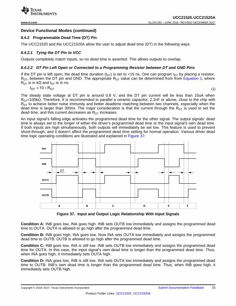
An input signal’s falling edge activates the programmed dead time for the other signal. The output signals’ deadtime is always set to the longer of either the driver’s programmed dead time or the input signal’s own dead time.If both inputs are high simultaneously, both outputs will immediately be set low. This feature is used to preventshoot-through, and it doesn’t affect the programmed dead time setting for normal operation. Various driver deadtime logic operating conditions are illustrated and explained in Figure 37:
Figure 37. Input and Output Logic Relationship With Input Signals
Condition A: INB goes low, INA goes high. INB sets OUTB low immediately and assigns the programmed deadtime to OUTA. OUTA is allowed to go high after the programmed dead time.
Condition B: INB goes high, INA goes low. Now INA sets OUTA low immediately and assigns the programmeddead time to OUTB. OUTB is allowed to go high after the programmed dead time.
Condition C: INB goes low, INA is still low. INB sets OUTB low immediately and assigns the programmed deadtime for OUTA. In this case, the input signal’s own dead time is longer than the programmed dead time. Thus,when INA goes high, it immediately sets OUTA high.
Condition D: INA goes low, INB is still low. INA sets OUTA low immediately and assigns the programmed deadtime to OUTB. INB’s own dead time is longer than the programmed dead time. Thus, when INB goes high, itimmediately sets OUTB high.
Device Functional Modes (continued)Condition E: INA goes high, while INB and OUTB are still high. To avoid overshoot, INA immediately pullsOUTB low and keeps OUTA low. After some time OUTB goes low and assigns the programmed dead time toOUTA. OUTB is already low. After the programmed dead time, OUTA is allowed to go high.
Condition F: INB goes high, while INA and OUTA are still high. To avoid overshoot, INB immediately pullsOUTA low and keeps OUTB low. After some time OUTA goes low and assigns the programmed dead time toOUTB. OUTA is already low. After the programmed dead time, OUTB is allowed to go high.
NOTEInformation in the following applications sections is not part of the TI componentspecification, and TI does not warrant its accuracy or completeness. TI’s customers areresponsible for determining suitability of components for their purposes. Customers shouldvalidate and test their design implementation to confirm system functionality.
9.1 Application Information
The UCC21520 or the UCC21520A effectively combines both isolation and buffer-drive functions. The flexible,universal capability of the UCC21520 and the UCC21520A (with up to 18-V VCCI and 25-V VDDA/VDDB) allowsthe device to be used as a low-side, high-side, high-side/low-side or half-bridge driver for MOSFETs, IGBTs orSiC MOSFETs. With integrated components, advanced protection features (UVLO, dead time, and disable) andoptimized switching performance; the UCC21520 and the UCC21520A enable designers to build smaller, morerobust designs for enterprise, telecom, automotive, and industrial applications with a faster time to market.
9.2 Typical ApplicationThe circuit in Figure 38 shows a reference design with the UCC21520 driving a typical half-bridge configurationwhich could be used in several popular power converter topologies such as synchronous buck, synchronousboost, half-bridge/full bridge isolated topologies, and 3-phase motor drive applications.
Typical Application (continued)9.2.1 Design RequirementsTable 4 lists reference design parameters for the example application: UCC21520 driving 1200-V SiC-MOSFETsin a high side-low side configuration.
Table 4. UCC21520 Design RequirementsPARAMETER VALUE UNITS
Power transistor C2M0080120D -VCC 5.0 VVDD 20 V
Input signal amplitude 3.3 VSwitching frequency (fs) 100 kHz
DC link voltage 800 V
9.2.2 Detailed Design Procedure
9.2.2.1 Designing INA/INB Input FilterIt is recommended that users avoid shaping the signals to the gate driver in an attempt to slow down (or delay)the signal at the output. However, a small input RIN-CIN filter can be used to filter out the ringing introduced bynon-ideal layout or long PCB traces.
Such a filter should use an RIN in the range of 0 Ω to100 Ω and a CIN between 10 pF and 100 pF. In theexample, an RIN = 51 Ω and a CIN = 33 pF are selected, with a corner frequency of approximately 100 MHz.
When selecting these components, it is important to pay attention to the trade-off between good noise immunityand propagation delay.
9.2.2.2 Select External Bootstrap Diode and its Series ResistorThe bootstrap capacitor is charged by VDD through an external bootstrap diode every cycle when the low sidetransistor turns on. Charging the capacitor involves high-peak currents, and therefore transient power dissipationin the bootstrap diode may be significant. Conduction loss also depends on the diode’s forward voltage drop.Both the diode conduction losses and reverse recovery losses contribute to the total losses in the gate drivercircuit.
When selecting external bootstrap diodes, it is recommended that one chose high voltage, fast recovery diodesor SiC Schottky diodes with a low forward voltage drop and low junction capacitance in order to minimize the lossintroduced by reverse recovery and related grounding noise bouncing. In the example, the DC-link voltage is 800VDC. The voltage rating of the bootstrap diode should be higher than the DC-link voltage with a good margin.Therefore, a 1200-V SiC diode, C4D02120E, is chosen in this example.
A bootstrap resistor, RBOOT, is used to reduce the inrush current in DBOOT and limit the ramp up slew rate ofvoltage of VDDA-VSSA during each switching cycle, especially when the VSSA(SW) pin has an excessivenegative transient voltage. The recommended value for RBOOT is between 1 Ω and 20 Ω depending on the diodeused. In the example, a current limiting resistor of 2.2 Ω is selected to limit the inrush current of bootstrap diode.The estimated worst case peak current through DBoot is,
where• VBDF is the estimated bootstrap diode forward voltage drop at 8 A. (2)
9.2.2.3 Gate Driver Output ResistorThe external gate driver resistors, RON/ROFF, are used to:1. Limit ringing caused by parasitic inductances/capacitances.
2. Limit ringing caused by high voltage/current switching dv/dt, di/dt, and body-diode reverse recovery.
3. Fine-tune gate drive strength, i.e. peak sink and source current to optimize the switching loss.
4. Reduce electromagnetic interference (EMI).
As mentioned in Output Stage, the UCC21520 has a pull-up structure with a P-channel MOSFET and anadditional pull-up N-channel MOSFET in parallel. The combined peak source current is 4 A. Therefore, the peaksource current can be predicted with:
(3)
where• RON: External turn-on resistance.• RGFET_INT: Power transistor internal gate resistance, found in the power transistor datasheet.• IO+ = Peak source current – The minimum value between 4 A, the gate driver peak source current, and the
calculated value based on the gate drive loop resistance. (4)
In this example:
(5)
(6)
Therefore, the high-side and low-side peak source current is 2.4 A and 2.5 A respectively. Similarly, the peaksink current can be calculated with:
(7)
where• ROFF: External turn-off resistance;• VGDF: The anti-parallel diode forward voltage drop which is in series with ROFF. The diode in this example is an
MSS1P4.• IO-: Peak sink current – the minimum value between 6 A, the gate driver peak sink current, and the calculated
value based on the gate drive loop resistance. (8)
Therefore, the high-side and low-side peak sink current is 3.6 A and 3.7 A respectively.
Importantly, the estimated peak current is also influenced by PCB layout and load capacitance. Parasiticinductance in the gate driver loop can slow down the peak gate drive current and introduce overshoot andundershoot. Therefore, it is strongly recommended that the gate driver loop should be minimized. On the otherhand, the peak source/sink current is dominated by loop parasitics when the load capacitance (CISS) of the powertransistor is very small (typically less than 1 nF), because the rising and falling time is too small and close to theparasitic ringing period.
9.2.2.4 Estimate Gate Driver Power LossThe total loss, PG, in the gate driver subsystem includes the power losses of the UCC21520 (PGD) and the powerlosses in the peripheral circuitry, such as the external gate drive resistor. Bootstrap diode loss is not included inPG and not discussed in this section.
PGD is the key power loss which determines the thermal safety-related limits of the UCC21520, and it can beestimated by calculating losses from several components.
The first component is the static power loss, PGDQ, which includes quiescent power loss on the driver as well asdriver self-power consumption when operating with a certain switching frequency. PGDQ is measured on thebench with no load connected to OUTA and OUTB at a given VCCI, VDDA/VDDB, switching frequency andambient temperature. Figure 4 shows the per output channel current consumption vs. operating frequency withno load. In this example, VVCCI = 5 V and VVDD = 20 V. The current on each power supply, with INA/INBswitching from 0 V to 3.3 V at 100 kHz is measured to be IVCCI = 2.5 mA, and IVDDA = IVDDB = 1.5 mA. Therefore,the PGDQ can be calculated with
(11)
The second component is switching operation loss, PGDO, with a given load capacitance which the driver chargesand discharges the load during each switching cycle. Total dynamic loss due to load switching, PGSW, can beestimated with
where• QG is the gate charge of the power transistor. (12)
If a split rail is used to turn on and turn off, then VDD is going to be equal to difference between the positive railto the negative rail.
QG represents the total gate charge of the power transistor switching 800 V at 20 A, and is subject to changewith different testing conditions. The UCC21520 gate driver loss on the output stage, PGDO, is part of PGSW. PGDOwill be equal to PGSW if the external gate driver resistances are zero, and all the gate driver loss is dissipatedinside the UCC21520. If there are external turn-on and turn-off resistances, the total loss will be distributedbetween the gate driver pull-up/down resistances and external gate resistances. Importantly, the pull-up/downresistance is a linear and fixed resistance if the source/sink current is not saturated to 4 A/6 A, however, it will benon-linear if the source/sink current is saturated. Therefore, PGDO is different in these two scenarios.
Case 1 - Linear Pull-Up/Down Resistor:
(14)
In this design example, all the predicted source/sink currents are less than 4 A/6 A, therefore, the UCC21520gate driver loss can be estimated with:
(15)
Case 2 - Nonlinear Pull-Up/Down Resistor:
where• VOUTA/B(t) is the gate driver OUTA and OUTB pin voltage during the turn on and off transient, and it can be
simplified that a constant current source (4 A at turn-on and 6 A at turn-off) is charging/discharging a loadcapacitor. Then, the VOUTA/B(t) waveform will be linear and the TR_Sys and TF_Sys can be easily predicted. (16)
For some scenarios, if only one of the pull-up or pull-down circuits is saturated and another one is not, the PGDOwill be a combination of Case 1 and Case 2, and the equations can be easily identified for the pull-up and pull-down based on the above discussion. Therefore, total gate driver loss dissipated in the gate driver UCC21520,PGD, is:
(17)
which is equal to 102 mW in the design example.
9.2.2.5 Estimating Junction TemperatureThe junction temperature (TJ) of the UCC21520 can be estimated with:
where• TC is the UCC21520 case-top temperature measured with a thermocouple or some other instrument, and• ΨJT is the Junction-to-top characterization parameter from the Thermal Information table. (18)
Using the junction-to-top characterization parameter (ΨJT) instead of the junction-to-case thermal resistance(RΘJC) can greatly improve the accuracy of the junction temperature estimation. The majority of the thermalenergy of most ICs is released into the PCB through the package leads, whereas only a small percentage of thetotal energy is released through the top of the case (where thermocouple measurements are usually conducted).RΘJC can only be used effectively when most of the thermal energy is released through the case, such as withmetal packages or when a heatsink is applied to an IC package. In all other cases, use of RΘJC will inaccuratelyestimate the true junction temperature. ΨJT is experimentally derived by assuming that the amount of energyleaving through the top of the IC will be similar in both the testing environment and the application environment.As long as the recommended layout guidelines are observed, junction temperature estimates can be madeaccurately to within a few degrees Celsius. For more information, see the Semiconductor and IC PackageThermal Metrics application report.
9.2.2.6 Selecting VCCI, VDDA/B CapacitorBypass capacitors for VCCI, VDDA, and VDDB are essential for achieving reliable performance. It isrecommended that one choose low ESR and low ESL surface-mount multi-layer ceramic capacitors (MLCC) withsufficient voltage ratings, temperature coefficients and capacitance tolerances. Importantly, DC bias on an MLCCwill impact the actual capacitance value. For example, a 25-V, 1-µF X7R capacitor is measured to be only 500nF when a DC bias of 15 VDC is applied.
9.2.2.6.1 Selecting a VCCI Capacitor
A bypass capacitor connected to VCCI supports the transient current needed for the primary logic and the totalcurrent consumption, which is only a few mA. Therefore, a 50-V MLCC with over 100 nF is recommended for thisapplication. If the bias power supply output is a relatively long distance from the VCCI pin, a tantalum orelectrolytic capacitor, with a value over 1 µF, should be placed in parallel with the MLCC.
9.2.2.6.2 Selecting a VDDA (Bootstrap) Capacitor
A VDDA capacitor, also referred to as a bootstrap capacitor in bootstrap power supply configurations, allows forgate drive current transients up to 6 A, and needs to maintain a stable gate drive voltage for the power transistor.
The total charge needed per switching cycle can be estimated with
where• QG: Gate charge of the power transistor.• IVDD: The channel self-current consumption with no load at 100kHz.• (19)
Therefore, the absolute minimum CBoot requirement is:
where• ΔVVDDA is the voltage ripple at VDDA, which is 0.5 V in this example. (20)
In practice, the value of CBoot is greater than the calculated value. This allows for the capacitance shift caused bythe DC bias voltage and for situations where the power stage would otherwise skip pulses due to load transients.Therefore, it is recommended to include a safety-related margin in the CBoot value and place it as close to theVDD and VSS pins as possible. A 50-V 1-µF capacitor is chosen in this example.
(21)
To further lower the AC impedance for a wide frequency range, it is recommended to have bypass capacitor witha low capacitance value, in this example a 100 nF, in parallel with CBoot to optimize the transient performance.
NOTEToo large CBOOT is not good. CBOOT may not be charged within the first few cycles andVBOOT could stay below UVLO. As a result, the high-side FET does not follow input signalcommand. Also during initial CBOOT charging cycles, the bootstrap diode has highestreverse recovery current and losses.
Chanel B has the same current requirements as Channel A, Therefore, a VDDB capacitor (Shown as CVDD inFigure 38) is needed. In this example with a bootstrap configuration, the VDDB capacitor will also supply currentfor VDDA through the bootstrap diode. A 50-V, 10-µF MLCC and a 50-V, 220-nF MLCC are chosen for CVDD. Ifthe bias power supply output is a relatively long distance from the VDDB pin, a tantalum or electrolytic capacitor,with a value over 10 µF, should be used in parallel with CVDD.
9.2.2.7 Dead Time Setting GuidelinesFor power converter topologies utilizing half-bridges, the dead time setting between the top and bottom transistoris important for preventing shoot-through during dynamic switching.
The UCC21520 dead time specification in the electrical table is defined as the time interval from 90% of onechannel’s falling edge to 10% of the other channel’s rising edge (see
Figure 30). This definition ensures that the dead time setting is independent of the load condition, andguarantees linearity through manufacture testing. However, this dead time setting may not reflect the dead timein the power converter system, since the dead time setting is dependent on the external gate drive turn-on/offresistor, DC-Link switching voltage/current, as well as the input capacitance of the load transistor.
Here is a suggestion on how to select an appropriate dead time for UCC21520:
where• DTsetting: UCC21520 dead time setting in ns, DTSetting = 10 × RDT(in kΩ).• DTReq: System required dead time between the real VGS signal of the top and bottom switch with enough
margin, or ZVS requirement.• TF_Sys: In-system gate turn-off falling time at worst case of load, voltage/current conditions.• TR_Sys: In-system gate turn-on rising time at worst case of load, voltage/current conditions.• TD(on): Turn-on delay time, from 10% of the transistor gate signal to power transistor gate threshold. (22)
In the example, DTSetting is set to 250 ns.
It should be noted that the UCC21520 dead time setting is decided by the DT pin configuration (SeeProgrammable Dead Time (DT) Pin), and it cannot automatically fine-tune the dead time based on systemconditions. It is recommended to parallel a ceramic capacitor, 2.2 nF or above, close to the DT pin with RDT toachieve better noise immunity.
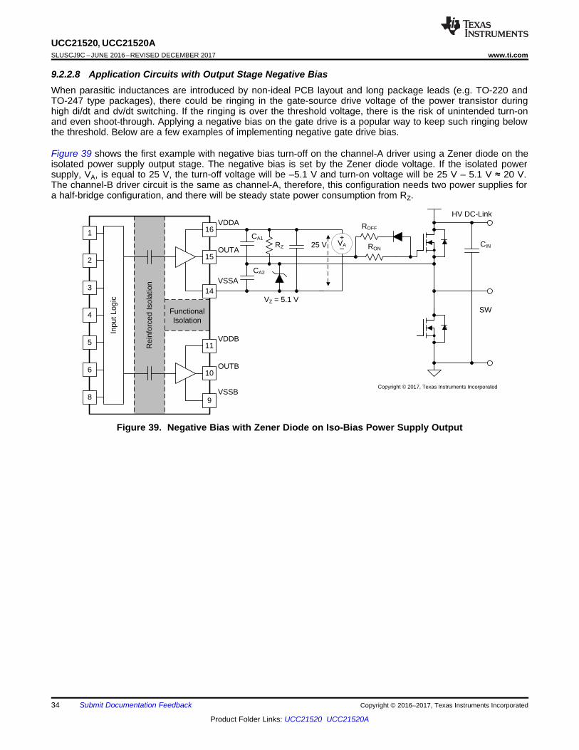
9.2.2.8 Application Circuits with Output Stage Negative BiasWhen parasitic inductances are introduced by non-ideal PCB layout and long package leads (e.g. TO-220 andTO-247 type packages), there could be ringing in the gate-source drive voltage of the power transistor duringhigh di/dt and dv/dt switching. If the ringing is over the threshold voltage, there is the risk of unintended turn-onand even shoot-through. Applying a negative bias on the gate drive is a popular way to keep such ringing belowthe threshold. Below are a few examples of implementing negative gate drive bias.
Figure 39 shows the first example with negative bias turn-off on the channel-A driver using a Zener diode on theisolated power supply output stage. The negative bias is set by the Zener diode voltage. If the isolated powersupply, VA, is equal to 25 V, the turn-off voltage will be –5.1 V and turn-on voltage will be 25 V – 5.1 V ≈ 20 V.The channel-B driver circuit is the same as channel-A, therefore, this configuration needs two power supplies fora half-bridge configuration, and there will be steady state power consumption from RZ.
Figure 39. Negative Bias with Zener Diode on Iso-Bias Power Supply Output
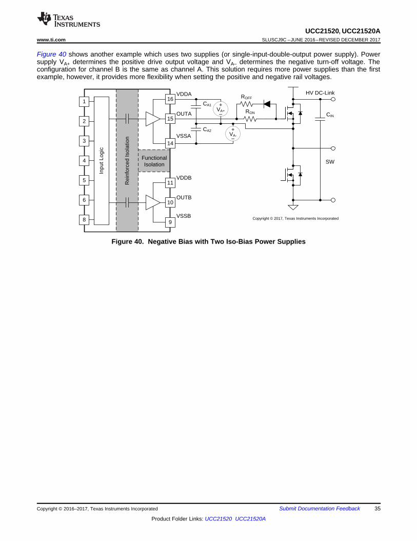
Figure 40 shows another example which uses two supplies (or single-input-double-output power supply). Powersupply VA+ determines the positive drive output voltage and VA– determines the negative turn-off voltage. Theconfiguration for channel B is the same as channel A. This solution requires more power supplies than the firstexample, however, it provides more flexibility when setting the positive and negative rail voltages.
Figure 40. Negative Bias with Two Iso-Bias Power Supplies
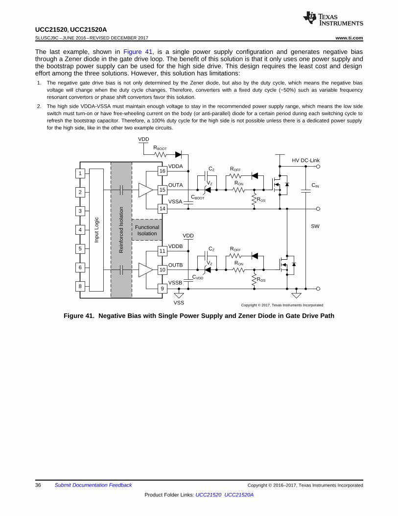
The last example, shown in Figure 41, is a single power supply configuration and generates negative biasthrough a Zener diode in the gate drive loop. The benefit of this solution is that it only uses one power supply andthe bootstrap power supply can be used for the high side drive. This design requires the least cost and designeffort among the three solutions. However, this solution has limitations:1. The negative gate drive bias is not only determined by the Zener diode, but also by the duty cycle, which means the negative bias
voltage will change when the duty cycle changes. Therefore, converters with a fixed duty cycle (~50%) such as variable frequencyresonant convertors or phase shift convertors favor this solution.
2. The high side VDDA-VSSA must maintain enough voltage to stay in the recommended power supply range, which means the low sideswitch must turn-on or have free-wheeling current on the body (or anti-parallel) diode for a certain period during each switching cycle torefresh the bootstrap capacitor. Therefore, a 100% duty cycle for the high side is not possible unless there is a dedicated power supplyfor the high side, like in the other two example circuits.
Figure 41. Negative Bias with Single Power Supply and Zener Diode in Gate Drive Path
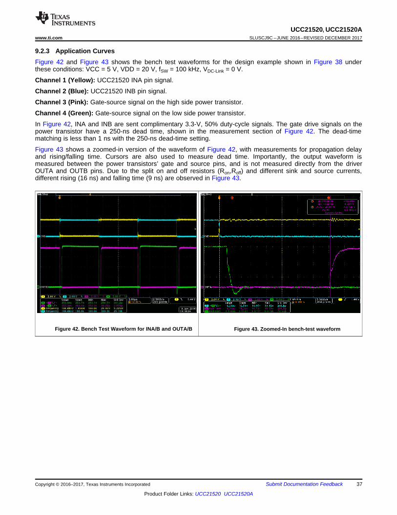
9.2.3 Application CurvesFigure 42 and Figure 43 shows the bench test waveforms for the design example shown in Figure 38 underthese conditions: VCC = 5 V, VDD = 20 V, fSW = 100 kHz, VDC-Link = 0 V.
Channel 1 (Yellow): UCC21520 INA pin signal.
Channel 2 (Blue): UCC21520 INB pin signal.
Channel 3 (Pink): Gate-source signal on the high side power transistor.
Channel 4 (Green): Gate-source signal on the low side power transistor.
In Figure 42, INA and INB are sent complimentary 3.3-V, 50% duty-cycle signals. The gate drive signals on thepower transistor have a 250-ns dead time, shown in the measurement section of Figure 42. The dead-timematching is less than 1 ns with the 250-ns dead-time setting.
Figure 43 shows a zoomed-in version of the waveform of Figure 42, with measurements for propagation delayand rising/falling time. Cursors are also used to measure dead time. Importantly, the output waveform ismeasured between the power transistors’ gate and source pins, and is not measured directly from the driverOUTA and OUTB pins. Due to the split on and off resistors (Ron,Roff) and different sink and source currents,different rising (16 ns) and falling time (9 ns) are observed in Figure 43.
Figure 42. Bench Test Waveform for INA/B and OUTA/B Figure 43. Zoomed-In bench-test waveform
10 Power Supply RecommendationsThe recommended input supply voltage (VCCI) for the UCC21520 and the UCC21520A is between 3 V and 18V. The output bias supply voltage (VDDA/VDDB) range depends on which version of UCC21520 one is using.The lower end of this bias supply range is governed by the internal under voltage lockout (UVLO) protectionfeature of each device. One mustn’t let VDD or VCCI fall below their respective UVLO thresholds (For moreinformation on UVLO see VDD, VCCI, and Under Voltage Lock Out (UVLO)). The upper end of the VDDA/VDDBrange depends on the maximum gate voltage of the power device being driven by the UCC21520 and theUCC21520A. The UCC21520 and the UCC21520A have a recommended maximum VDDA/VDDB of 25 V.
A local bypass capacitor should be placed between the VDD and VSS pins. This capacitor should be positionedas close to the device as possible. A low ESR, ceramic surface mount capacitor is recommended. It is furthersuggested that one place two such capacitors: one with a value of ≈10-µF for device biasing, and an additional≤100-nF capacitor in parallel for high frequency filtering.
Similarly, a bypass capacitor should also be placed between the VCCI and GND pins. Given the small amount ofcurrent drawn by the logic circuitry within the input side of the UCC21520 and the UCC21520A, this bypasscapacitor has a minimum recommended value of 100 nF.
11.1 Layout GuidelinesOne must pay close attention to PCB layout in order to achieve optimum performance for the UCC21520 and theUCC21520A. Below are some key points.
Component Placement:• Low-ESR and low-ESL capacitors must be connected close to the device between the VCCI and GND pins
and between the VDD and VSS pins to support high peak currents when turning on the external powertransistor.
• To avoid large negative transients on the switch node VSSA (HS) pin, the parasitic inductances between thesource of the top transistor and the source of the bottom transistor must be minimized.
• It is recommended to place the dead-time setting resistor, RDT, and its bypassing capacitor close to DT pin ofthe UCC21520 or the UCC21520A.
• It is recommended to bypass using a ≈1nF low ESR/ESL capacitor, CDIS, close to DIS pin when connecting toa µC with distance.
Grounding Considerations:• It is essential to confine the high peak currents that charge and discharge the transistor gates to a minimal
physical area. This will decrease the loop inductance and minimize noise on the gate terminals of thetransistors. The gate driver must be placed as close as possible to the transistors.
• Pay attention to high current path that includes the bootstrap capacitor, bootstrap diode, local VSSB-referenced bypass capacitor, and the low-side transistor body/anti-parallel diode. The bootstrap capacitor isrecharged on a cycle-by-cycle basis through the bootstrap diode by the VDD bypass capacitor. Thisrecharging occurs in a short time interval and involves a high peak current. Minimizing this loop length andarea on the circuit board is important for ensuring reliable operation.
High-Voltage Considerations:• To ensure isolation performance between the primary and secondary side, one should avoid placing any PCB
traces or copper below the driver device. A PCB cutout is recommended in order to prevent contaminationthat may compromise the UCC21520’s and the UCC21520A’s isolation performance.
• For half-bridge, or high-side/low-side configurations, where the channel A and channel B drivers couldoperate with a DC-link voltage up to 1500 VDC, one should try to increase the creepage distance of the PCBlayout between the high and low-side PCB traces.
Thermal Considerations:• A large amount of power may be dissipated by the UCC21520 or the UCC21520A if the driving voltage is
high, the load is heavy, or the switching frequency is high (refer to Estimate Gate Driver Power Loss for moredetails). Proper PCB layout can help dissipate heat from the device to the PCB and minimize junction toboard thermal impedance (θJB).
• Increasing the PCB copper connecting to VDDA, VDDB, VSSA and VSSB pins is recommended, with priorityon maximizing the connection to VSSA and VSSB (see Figure 45 and Figure 46). However, high voltage PCBconsiderations mentioned above must be maintained.
• If there are multiple layers in the system, it is also recommended to connect the VDDA, VDDB, VSSA andVSSB pins to internal ground or power planes through multiple vias of adequate size. However, keep in mindthat there shouldn’t be any traces/coppers from different high voltage planes overlapping.
Layout Example (continued)PCB traces between the high-side and low-side gate drivers in the output stage are increased to maximize thecreepage distance for high-voltage operation, which will also minimize cross-talk between the switching nodeVSSA (SW), where high dv/dt may exist, and the low-side gate drive due to the parasitic capacitance coupling.
Figure 45. Top Layer Traces and Copper Figure 46. Bottom Layer Traces and Copper
Figure 47 and Figure 48 are 3D layout pictures with top view and bottom views.
NOTEThe location of the PCB cutout between the primary side and secondary sides, whichensures isolation performance.
12.3 Receiving Notification of Documentation UpdatesTo receive notification of documentation updates, navigate to the device product folder on ti.com. In the upperright corner, click on Alert me to register and receive a weekly digest of any product information that haschanged. For change details, review the revision history included in any revised document.
12.4 Community ResourcesThe following links connect to TI community resources. Linked contents are provided "AS IS" by the respectivecontributors. They do not constitute TI specifications and do not necessarily reflect TI's views; see TI's Terms ofUse.
TI E2E™ Online Community TI's Engineer-to-Engineer (E2E) Community. Created to foster collaborationamong engineers. At e2e.ti.com, you can ask questions, share knowledge, explore ideas and helpsolve problems with fellow engineers.
Design Support TI's Design Support Quickly find helpful E2E forums along with design support tools andcontact information for technical support.
12.5 TrademarksE2E is a trademark of Texas Instruments.All other trademarks are the property of their respective owners.
12.6 Electrostatic Discharge CautionThese devices have limited built-in ESD protection. The leads should be shorted together or the device placed in conductive foamduring storage or handling to prevent electrostatic damage to the MOS gates.
12.7 GlossarySLYZ022 — TI Glossary.
This glossary lists and explains terms, acronyms, and definitions.
13 Mechanical, Packaging, and Orderable InformationThe following pages include mechanical, packaging, and orderable information. This information is the mostcurrent data available for the designated devices. This data is subject to change without notice and revision ofthis document. For browser-based versions of this data sheet, refer to the left-hand navigation.
UCC21520ADW ACTIVE SOIC DW 16 40 Green (RoHS& no Sb/Br)
CU NIPDAU Level-2-260C-1 YEAR -40 to 125 UCC21520A
UCC21520ADWR ACTIVE SOIC DW 16 2000 Green (RoHS& no Sb/Br)
CU NIPDAU Level-2-260C-1 YEAR -40 to 125 UCC21520A
UCC21520DW ACTIVE SOIC DW 16 40 Green (RoHS& no Sb/Br)
CU NIPDAU Level-2-260C-1 YEAR -40 to 125 UCC21520
UCC21520DWR ACTIVE SOIC DW 16 2000 Green (RoHS& no Sb/Br)
CU NIPDAU Level-2-260C-1 YEAR -40 to 125 UCC21520
(1) The marketing status values are defined as follows:ACTIVE: Product device recommended for new designs.LIFEBUY: TI has announced that the device will be discontinued, and a lifetime-buy period is in effect.NRND: Not recommended for new designs. Device is in production to support existing customers, but TI does not recommend using this part in a new design.PREVIEW: Device has been announced but is not in production. Samples may or may not be available.OBSOLETE: TI has discontinued the production of the device.
(2) RoHS: TI defines "RoHS" to mean semiconductor products that are compliant with the current EU RoHS requirements for all 10 RoHS substances, including the requirement that RoHS substancedo not exceed 0.1% by weight in homogeneous materials. Where designed to be soldered at high temperatures, "RoHS" products are suitable for use in specified lead-free processes. TI mayreference these types of products as "Pb-Free".RoHS Exempt: TI defines "RoHS Exempt" to mean products that contain lead but are compliant with EU RoHS pursuant to a specific EU RoHS exemption.Green: TI defines "Green" to mean the content of Chlorine (Cl) and Bromine (Br) based flame retardants meet JS709B low halogen requirements of <=1000ppm threshold. Antimony trioxide basedflame retardants must also meet the <=1000ppm threshold requirement.
(3) MSL, Peak Temp. - The Moisture Sensitivity Level rating according to the JEDEC industry standard classifications, and peak solder temperature.
(4) There may be additional marking, which relates to the logo, the lot trace code information, or the environmental category on the device.
(5) Multiple Device Markings will be inside parentheses. Only one Device Marking contained in parentheses and separated by a "~" will appear on a device. If a line is indented then it is a continuationof the previous line and the two combined represent the entire Device Marking for that device.
(6) Lead/Ball Finish - Orderable Devices may have multiple material finish options. Finish options are separated by a vertical ruled line. Lead/Ball Finish values may wrap to two lines if the finishvalue exceeds the maximum column width.
Important Information and Disclaimer:The information provided on this page represents TI's knowledge and belief as of the date that it is provided. TI bases its knowledge and belief on informationprovided by third parties, and makes no representation or warranty as to the accuracy of such information. Efforts are underway to better integrate information from third parties. TI has taken and
continues to take reasonable steps to provide representative and accurate information but may not have conducted destructive testing or chemical analysis on incoming materials and chemicals.TI and TI suppliers consider certain information to be proprietary, and thus CAS numbers and other limited information may not be available for release.
In no event shall TI's liability arising out of such information exceed the total purchase price of the TI part(s) at issue in this document sold by TI to Customer on an annual basis.
OTHER QUALIFIED VERSIONS OF UCC21520 :
• Automotive: UCC21520-Q1
NOTE: Qualified Version Definitions:
• Automotive - Q100 devices qualified for high-reliability automotive applications targeting zero defects
Images above are just a representation of the package family, actual package may vary.Refer to the product data sheet for package details.
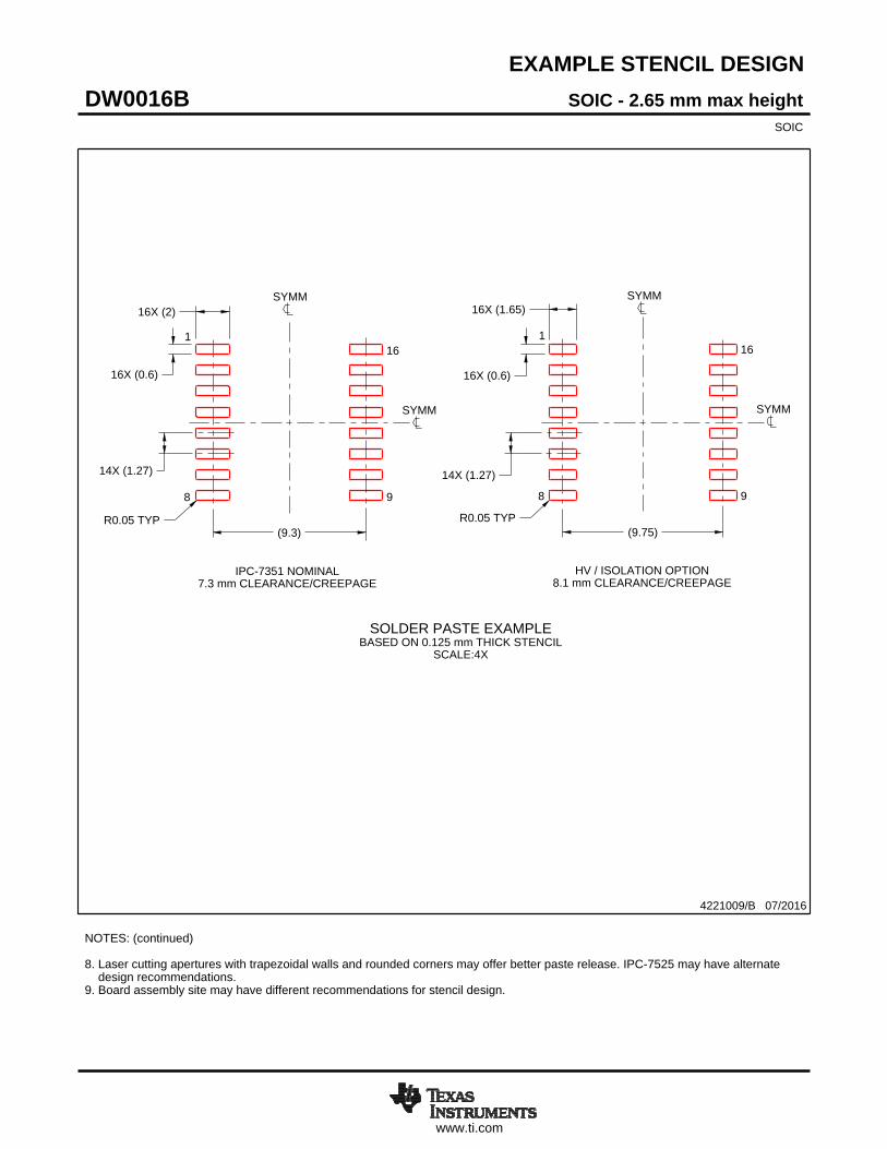
DW 16 SOIC - 2.65 mm max heightSMALL OUTLINE INTEGRATED CIRCUIT
4040000-2/H
www.ti.com
PACKAGE OUTLINE
C
TYP10.639.97
2.65 MAX
14X 1.27
16X 0.510.31
2X8.89
TYP0.330.10
0 - 80.30.1
(1.4)
0.25GAGE PLANE
1.270.40
A
NOTE 3
10.510.1
BNOTE 4
7.67.4
4221009/B 07/2016
SOIC - 2.65 mm max heightDW0016BSOIC
NOTES: 1. All linear dimensions are in millimeters. Dimensions in parenthesis are for reference only. Dimensioning and tolerancing per ASME Y14.5M. 2. This drawing is subject to change without notice. 3. This dimension does not include mold flash, protrusions, or gate burrs. Mold flash, protrusions, or gate burrs shall not exceed 0.15 mm, per side. 4. This dimension does not include interlead flash. Interlead flash shall not exceed 0.25 mm, per side.5. Reference JEDEC registration MS-013.
1 16
0.25 C A B
98
PIN 1 IDAREA
SEATING PLANE
0.1 C
SEE DETAIL A
DETAIL ATYPICAL
SCALE 1.500
www.ti.com
EXAMPLE BOARD LAYOUT
(9.75)R0.05 TYP
0.07 MAXALL AROUND
0.07 MINALL AROUND
(9.3)
14X (1.27)
R0.05 TYP
16X (1.65)
16X (0.6)
14X (1.27)
16X (2)
16X (0.6)
4221009/B 07/2016
SOIC - 2.65 mm max heightDW0016BSOIC
SYMM
SYMM
SEEDETAILS
1
8 9
16
SYMM
HV / ISOLATION OPTION8.1 mm CLEARANCE/CREEPAGE
NOTES: (continued) 6. Publication IPC-7351 may have alternate designs. 7. Solder mask tolerances between and around signal pads can vary based on board fabrication site.
METAL SOLDER MASKOPENING
NON SOLDER MASKDEFINED
SOLDER MASK DETAILS
OPENINGSOLDER MASK METAL
SOLDER MASKDEFINED
LAND PATTERN EXAMPLESCALE:4X
SYMM
1
8 9
16
IPC-7351 NOMINAL7.3 mm CLEARANCE/CREEPAGE
SEEDETAILS
www.ti.com
EXAMPLE STENCIL DESIGN
R0.05 TYPR0.05 TYP
16X (1.65)
16X (0.6)
14X (1.27)
(9.75)
16X (2)
16X (0.6)
14X (1.27)
(9.3)
4221009/B 07/2016
SOIC - 2.65 mm max heightDW0016BSOIC
NOTES: (continued) 8. Laser cutting apertures with trapezoidal walls and rounded corners may offer better paste release. IPC-7525 may have alternate design recommendations. 9. Board assembly site may have different recommendations for stencil design.
SYMM
SYMM
1
8 9
16
HV / ISOLATION OPTION8.1 mm CLEARANCE/CREEPAGE
SOLDER PASTE EXAMPLEBASED ON 0.125 mm THICK STENCIL
SCALE:4X
SYMM
SYMM
1
8 9
16
IPC-7351 NOMINAL7.3 mm CLEARANCE/CREEPAGE
IMPORTANT NOTICE
Texas Instruments Incorporated (TI) reserves the right to make corrections, enhancements, improvements and other changes to itssemiconductor products and services per JESD46, latest issue, and to discontinue any product or service per JESD48, latest issue. Buyersshould obtain the latest relevant information before placing orders and should verify that such information is current and complete.TI’s published terms of sale for semiconductor products (http://www.ti.com/sc/docs/stdterms.htm) apply to the sale of packaged integratedcircuit products that TI has qualified and released to market. Additional terms may apply to the use or sale of other types of TI products andservices.Reproduction of significant portions of TI information in TI data sheets is permissible only if reproduction is without alteration and isaccompanied by all associated warranties, conditions, limitations, and notices. TI is not responsible or liable for such reproduceddocumentation. Information of third parties may be subject to additional restrictions. Resale of TI products or services with statementsdifferent from or beyond the parameters stated by TI for that product or service voids all express and any implied warranties for theassociated TI product or service and is an unfair and deceptive business practice. TI is not responsible or liable for any such statements.Buyers and others who are developing systems that incorporate TI products (collectively, “Designers”) understand and agree that Designersremain responsible for using their independent analysis, evaluation and judgment in designing their applications and that Designers havefull and exclusive responsibility to assure the safety of Designers' applications and compliance of their applications (and of all TI productsused in or for Designers’ applications) with all applicable regulations, laws and other applicable requirements. Designer represents that, withrespect to their applications, Designer has all the necessary expertise to create and implement safeguards that (1) anticipate dangerousconsequences of failures, (2) monitor failures and their consequences, and (3) lessen the likelihood of failures that might cause harm andtake appropriate actions. Designer agrees that prior to using or distributing any applications that include TI products, Designer willthoroughly test such applications and the functionality of such TI products as used in such applications.TI’s provision of technical, application or other design advice, quality characterization, reliability data or other services or information,including, but not limited to, reference designs and materials relating to evaluation modules, (collectively, “TI Resources”) are intended toassist designers who are developing applications that incorporate TI products; by downloading, accessing or using TI Resources in anyway, Designer (individually or, if Designer is acting on behalf of a company, Designer’s company) agrees to use any particular TI Resourcesolely for this purpose and subject to the terms of this Notice.TI’s provision of TI Resources does not expand or otherwise alter TI’s applicable published warranties or warranty disclaimers for TIproducts, and no additional obligations or liabilities arise from TI providing such TI Resources. TI reserves the right to make corrections,enhancements, improvements and other changes to its TI Resources. TI has not conducted any testing other than that specificallydescribed in the published documentation for a particular TI Resource.Designer is authorized to use, copy and modify any individual TI Resource only in connection with the development of applications thatinclude the TI product(s) identified in such TI Resource. NO OTHER LICENSE, EXPRESS OR IMPLIED, BY ESTOPPEL OR OTHERWISETO ANY OTHER TI INTELLECTUAL PROPERTY RIGHT, AND NO LICENSE TO ANY TECHNOLOGY OR INTELLECTUAL PROPERTYRIGHT OF TI OR ANY THIRD PARTY IS GRANTED HEREIN, including but not limited to any patent right, copyright, mask work right, orother intellectual property right relating to any combination, machine, or process in which TI products or services are used. Informationregarding or referencing third-party products or services does not constitute a license to use such products or services, or a warranty orendorsement thereof. Use of TI Resources may require a license from a third party under the patents or other intellectual property of thethird party, or a license from TI under the patents or other intellectual property of TI.TI RESOURCES ARE PROVIDED “AS IS” AND WITH ALL FAULTS. TI DISCLAIMS ALL OTHER WARRANTIES ORREPRESENTATIONS, EXPRESS OR IMPLIED, REGARDING RESOURCES OR USE THEREOF, INCLUDING BUT NOT LIMITED TOACCURACY OR COMPLETENESS, TITLE, ANY EPIDEMIC FAILURE WARRANTY AND ANY IMPLIED WARRANTIES OFMERCHANTABILITY, FITNESS FOR A PARTICULAR PURPOSE, AND NON-INFRINGEMENT OF ANY THIRD PARTY INTELLECTUALPROPERTY RIGHTS. TI SHALL NOT BE LIABLE FOR AND SHALL NOT DEFEND OR INDEMNIFY DESIGNER AGAINST ANY CLAIM,INCLUDING BUT NOT LIMITED TO ANY INFRINGEMENT CLAIM THAT RELATES TO OR IS BASED ON ANY COMBINATION OFPRODUCTS EVEN IF DESCRIBED IN TI RESOURCES OR OTHERWISE. IN NO EVENT SHALL TI BE LIABLE FOR ANY ACTUAL,DIRECT, SPECIAL, COLLATERAL, INDIRECT, PUNITIVE, INCIDENTAL, CONSEQUENTIAL OR EXEMPLARY DAMAGES INCONNECTION WITH OR ARISING OUT OF TI RESOURCES OR USE THEREOF, AND REGARDLESS OF WHETHER TI HAS BEENADVISED OF THE POSSIBILITY OF SUCH DAMAGES.Unless TI has explicitly designated an individual product as meeting the requirements of a particular industry standard (e.g., ISO/TS 16949and ISO 26262), TI is not responsible for any failure to meet such industry standard requirements.Where TI specifically promotes products as facilitating functional safety or as compliant with industry functional safety standards, suchproducts are intended to help enable customers to design and create their own applications that meet applicable functional safety standardsand requirements. Using products in an application does not by itself establish any safety features in the application. Designers mustensure compliance with safety-related requirements and standards applicable to their applications. Designer may not use any TI products inlife-critical medical equipment unless authorized officers of the parties have executed a special contract specifically governing such use.Life-critical medical equipment is medical equipment where failure of such equipment would cause serious bodily injury or death (e.g., lifesupport, pacemakers, defibrillators, heart pumps, neurostimulators, and implantables). Such equipment includes, without limitation, allmedical devices identified by the U.S. Food and Drug Administration as Class III devices and equivalent classifications outside the U.S.TI may expressly designate certain products as completing a particular qualification (e.g., Q100, Military Grade, or Enhanced Product).Designers agree that it has the necessary expertise to select the product with the appropriate qualification designation for their applicationsand that proper product selection is at Designers’ own risk. Designers are solely responsible for compliance with all legal and regulatoryrequirements in connection with such selection.Designer will fully indemnify TI and its representatives against any damages, costs, losses, and/or liabilities arising out of Designer’s non-compliance with the terms and provisions of this Notice.