Features R&TTE (EN 300 220) / RoHS compliant 1 mW / 10 mW selectable Frequency selection free in 11 channels for 458 MHz High sensitivity receiver FM narrow band modulation
Applications Radio remote control cranes and machines Factory automation M2M Security systems Alarms Telemetry systems
For the CDP-TX/RX-02E-R, frequency setting is performed with the 4-bit switches. Instead of these 4-bit switches, the CDP-TX/RX-02EP-R has 8-pin connectors for frequency setting, making it possible to set the channels externally. There are no other technical and mechanical differences between CDP-TX/RX-02E-R and CDP-TX/RX-02EP-R.
General description
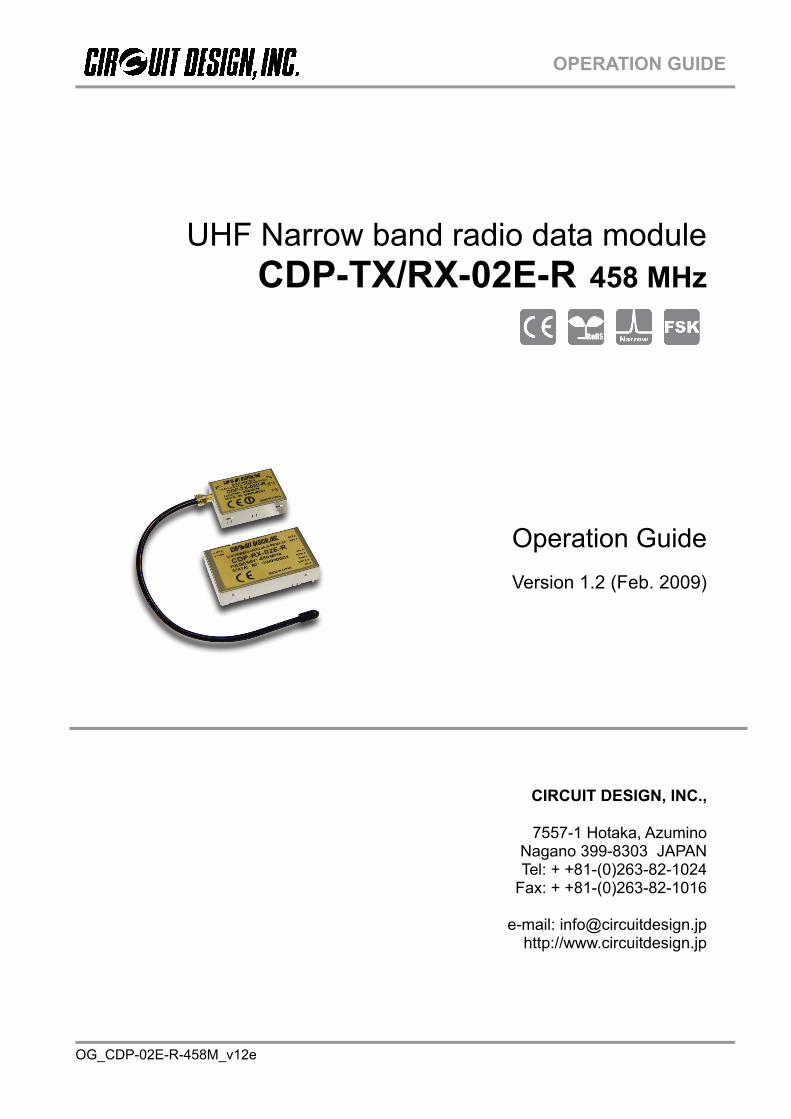
The CDP-TX-02E-R and CDP-RX-02E-R are an RoHS compliant, embedded industrial narrowband FM radio transmitter and receiver. They are suitable for various application fields such as wireless data communication, remote control, telemetry or wireless security systems. They are easy to use and integrate into application systems. Both CDP-TX-02E-R and CDP-RX-02E-R are equipped with a frequency synthesizer system with micro controller. Available frequency ranges are from 458.525 MHz to 458.775 MHz (11 channels). The compact size, low operating voltage and frequency selectability of the CDP-02E-R make it ideal for various applications where its interference rejection and practical distance range is far better than similar RF modules based on wide band SAW-resonator frequency generators. The CDP-RX-02E-R receiver has excellent blocking and adjacent channel selectivity.
OPERATION GUIDE.
OG_CDP-02E-R-458M_v12e Circuit Design, Inc. 4
SPECIFICATIONS CDP-TX-02E(P)-R Transmitter All ratings at 25°C +/- 5°C unless otherwise noted Parameter Rating Conditions General characteristics Applicable standard EN 300 220 -2 Ver.2.1.1 Communication method One way Emission class F1D Operating frequency range 458.525 – 458.775 MHz Operating temperature range -20 to + 60°C No dew condensation Storage temperature range -30 to + 70°C No dew condensation Aging rate Max. +/- 1 ppm / year Initial frequency tolerance Max. +/- 2 ppm At delivery *1 Dimension 26 x 36 x 10 mm Excluding protrusion Weight 14 g Not including the antenna Electrical specification Oscillation system PLL controlled VCO Channel steps 25 kHz Number of RF channels 11 channels Default channel at delivery (458.775 MHz) Data rate 300 to 4800 bps (Pulse length Min. 208 us Max. 20 ms) DI input level L = Gnd H = 3V to Vcc Data polarity Positive TX DI vs RX DO PLL reference frequency 21.25 kHz TCXO Antenna impedance 50 ohm Nominal Operating voltage 3 – 12 V
Typ. 43 mA At 10 mW / 3 V Max. 47 mA Consumption current Typ. 33 mA At 1 mW / 3V Max. 37 mA Transmitter part RF output power 10 mW / 1mW Selectable Frequency stability Max. +/- 4 ppm - 20 to 60°C with reference frequency at 25°C Deviation +/- 2.1 kHz +/-0.4 kHz PN9, 4800 bps, LPF 20 kHz, (-20 to + 60°C) Residual FM noise 0.17 kHz DI = L, LPF 20 kHz Modulation freq. characteristics +/- 3 dB 50 to 2400 Hz
Adjacent ch leakage power -37 dBm CH 25 kHz, BW 16 kHz, PN9, 4800 bps 50 ms From power on *2 Start up time 35 ms Time required for channel change (50 kHz step) *3
Specifications are subject to change without prior notice *1 Initial frequency tolerance: At delivery Initial frequency tolerance is defined as frequency drift at delivery within 1 year after the final adjustment *2 Start up time from power on Time required for the TX frequency to reach within +/-1.5ppm of a stable frequency after power on *3 Start up time for channel change Time required for the TX frequency to reach within +/-1.5ppm of a stable frequency after channel is selected
OPERATION GUIDE.
OG_CDP-02E-R-458M_v12e Circuit Design, Inc. 5
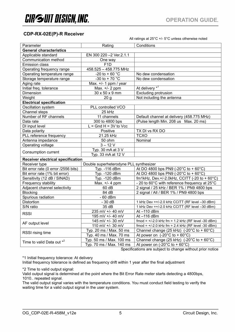
CDP-RX-02E(P)-R Receiver
All ratings at 25°C +/- 5°C unless otherwise noted
Parameter Rating Conditions General characteristics Applicable standard EN 300 220 –2 Ver.2.1.1 Communication method One way Emission class F1D Operating frequency range 458.525 – 458.775 MHz Operating temperature range -20 to + 60 °C No dew condensation Storage temperature range -30 to + 70 °C No dew condensation Aging rate Max. +/- 1 ppm / year Initial freq. tolerance Max. +/- 2 ppm At delivery *1 Dimension 30 x 50 x 9 mm Excluding protrusion Weight 20 g Not including the antenna Electrical specification Oscillation system PLL controlled VCO Channel steps 25 kHz Number of RF channels 11 channels Default channel at delivery (458.775 MHz) Data rate 300 to 4800 bps (Pulse length Min. 208 us Max. 20 ms) DI input level L = Gnd H = 3V to Vcc Data polarity Positive TX DI vs RX DO PLL reference frequency 21.25 kHz TCXO Antenna impedance 50 ohm Nominal Operating voltage 3 – 12 V
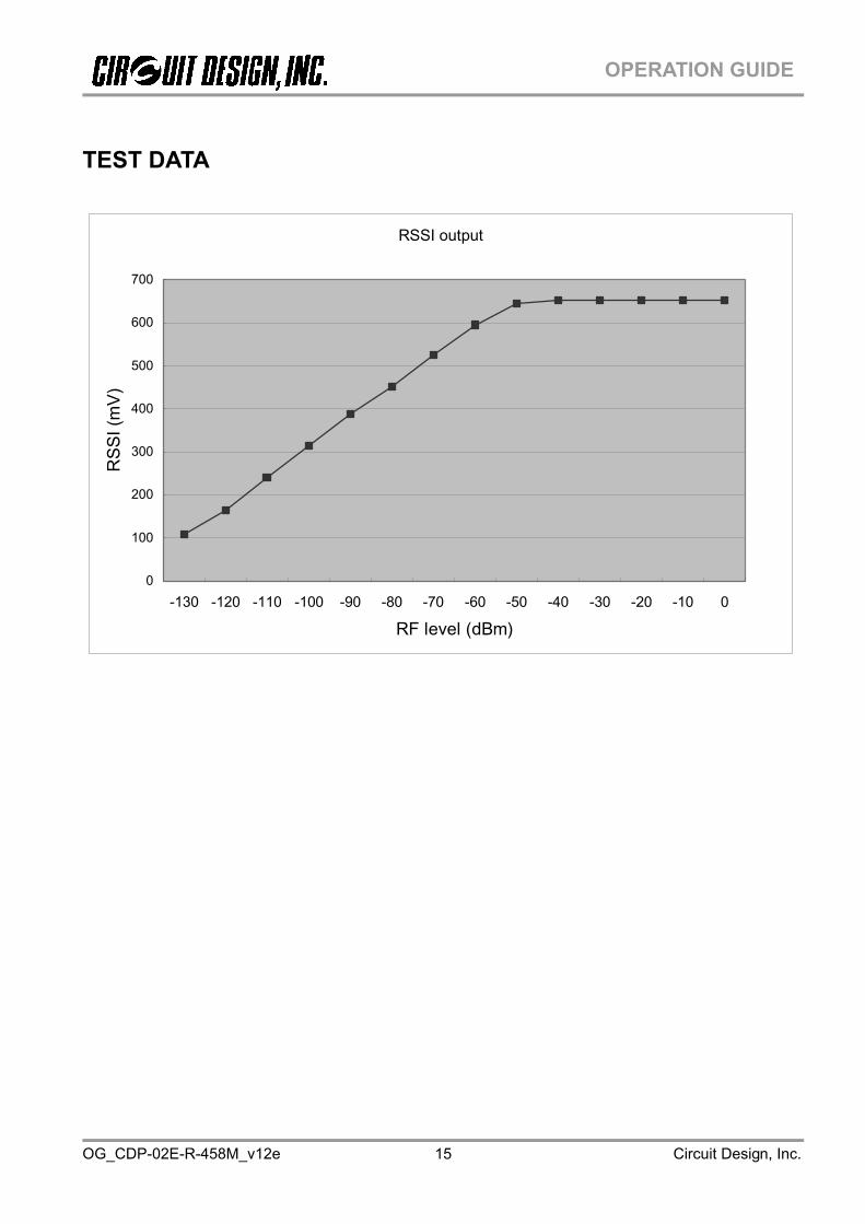
Typ. 30 mA at 3 V Consumption current Typ. 33 mA at 12 V Receiver electrical specification Receiver type Double superheterodyne PLL synthesizer Bit error rate (0 error /2556 bits) Typ. -116 dBm At DO 4800 bps PN9 (-20°C to + 60°C) Bit error rate (1% bit error) Typ. -120 dBm At DO 4800 bps PN9 (-20°C to + 60°C) Sensitivity (12 dB / SINAD) Typ. -120 dBm fm1kHz, Dev.+/-2.0kHz, CCITT (-20 to + 60°C)Frequency stability Max. +/- 4 ppm - 20 to 60°C with reference frequency at 25°C Adjacent channel selectivity 60 dB 2 signal / 25 kHz / BER 1% / PN9 4800 bps Blocking 84 dB 2 signal / All / BER 1% / PN9 4800 bps Spurious radiation - 60 dBm Distortion - 30 dB 1 kHz Dev =+/-2.0 kHz CCITT (RF level –30 dBm) S/N ratio 35 dB 1 kHz Dev =+/-2.0 kHz CCITT (RF level –30 dBm)
Typ. 20 ms / Max. 50 ms Channel change (25 kHz) (-20°C to + 60°C) RSSI rising time Typ. 40 ms / Max. 70 ms At power on (-20°C to + 60°C) Typ. 50 ms / Max. 100 ms Channel change (25 kHz) (-20°C to + 60°C) Time to valid Data out *2 Typ. 70 ms / Max. 140 ms At power on (-20°C to + 60°C)
Specifications are subject to change without prior notice
*1 Initial frequency tolerance: At delivery Initial frequency tolerance is defined as frequency drift within 1 year after the final adjustment *2 Time to valid output signal: Valid output signal is determined at the point where the Bit Error Rate meter starts detecting a 4800bps, 1010.. repeated signal. The valid output signal varies with the temperature conditions. You must conduct field testing to verify the waiting time for a valid output signal in the user system.
OPERATION GUIDE.
OG_CDP-02E-R-458M_v12e Circuit Design, Inc. 6
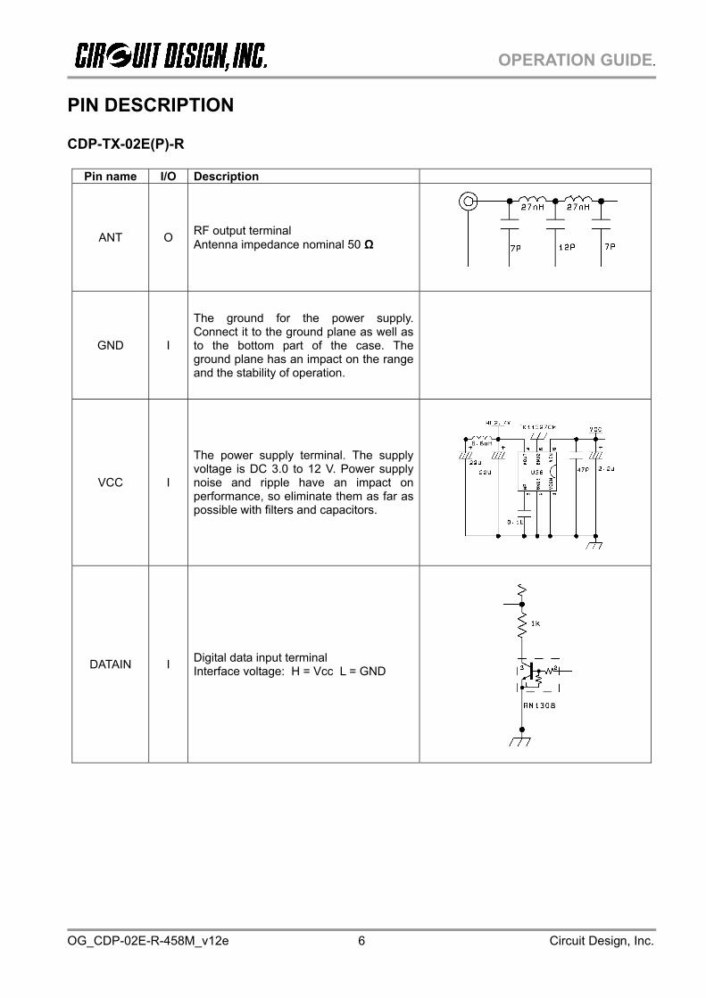
PIN DESCRIPTION CDP-TX-02E(P)-R
Pin name I/O Description
ANT O RF output terminal Antenna impedance nominal 50 Ω
GND I
The ground for the power supply. Connect it to the ground plane as well as to the bottom part of the case. The ground plane has an impact on the range and the stability of operation.
VCC I
The power supply terminal. The supply voltage is DC 3.0 to 12 V. Power supply noise and ripple have an impact on performance, so eliminate them as far as possible with filters and capacitors.
DATAIN I Digital data input terminal Interface voltage: H = Vcc L = GND
OPERATION GUIDE.
OG_CDP-02E-R-458M_v12e Circuit Design, Inc. 7
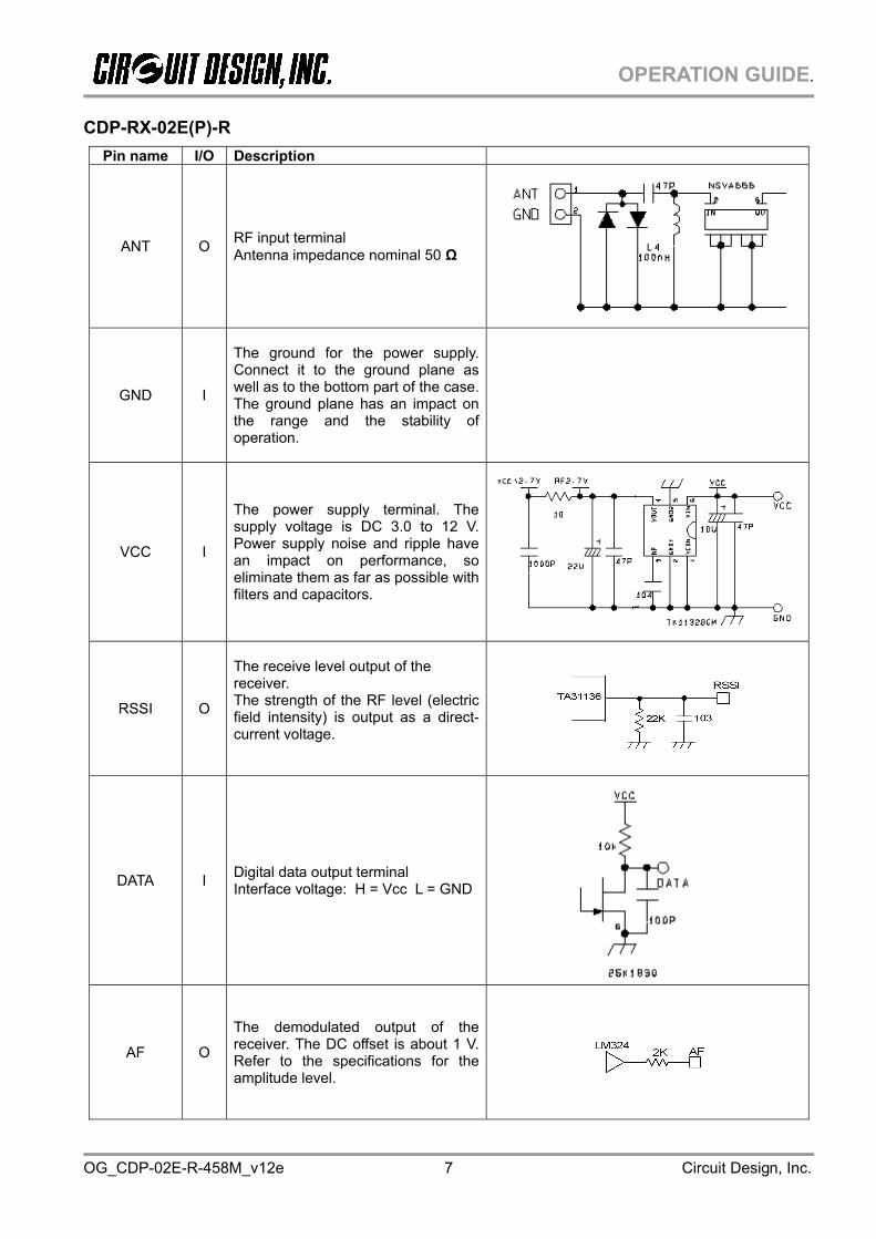
CDP-RX-02E(P)-R
Pin name I/O Description
ANT O RF input terminal Antenna impedance nominal 50 Ω
GND I
The ground for the power supply. Connect it to the ground plane as well as to the bottom part of the case. The ground plane has an impact on the range and the stability of operation.
VCC I
The power supply terminal. The supply voltage is DC 3.0 to 12 V. Power supply noise and ripple have an impact on performance, so eliminate them as far as possible with filters and capacitors.
RSSI O
The receive level output of the receiver. The strength of the RF level (electric field intensity) is output as a direct-current voltage.
DATA I Digital data output terminal Interface voltage: H = Vcc L = GND
AF O
The demodulated output of the receiver. The DC offset is about 1 V. Refer to the specifications for the amplitude level.
OPERATION GUIDE.
OG_CDP-02E-R-458M_v12e Circuit Design, Inc. 8
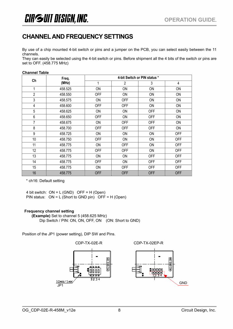
CHANNEL AND FREQUENCY SETTINGS By use of a chip mounted 4-bit switch or pins and a jumper on the PCB, you can select easily between the 11 channels. They can easily be selected using the 4-bit switch or pins. Before shipment all the 4 bits of the switch or pins are set to OFF. (458.775 MHz) Channel Table
4-bit Switch or PIN status * Ch Freq.
(MHz) 1 2 3 4 1 458.525 ON ON ON ON 2 458.550 OFF ON ON ON 3 458.575 ON OFF ON ON 4 458.600 OFF OFF ON ON 5 458.625 ON ON OFF ON 6 458.650 OFF ON OFF ON 7 458.675 ON OFF OFF ON 8 458.700 OFF OFF OFF ON 9 458.725 ON ON ON OFF 10 458.750 OFF ON ON OFF 11 458.775 ON OFF ON OFF 12 458.775 OFF OFF ON OFF 13 458.775 ON ON OFF OFF 14 458.775 OFF ON OFF OFF 15 458.775 ON OFF OFF OFF 16 458.775 OFF OFF OFF OFF
* ch16: Default setting
4 bit switch: ON = L (GND) OFF = H (Open) PIN status: ON = L (Short to GND pin) OFF = H (Open)
Frequency channel setting
(Example) Set to channel 5 (458.625 MHz) Dip Switch / PIN: ON, ON, OFF, ON (ON: Short to GND)
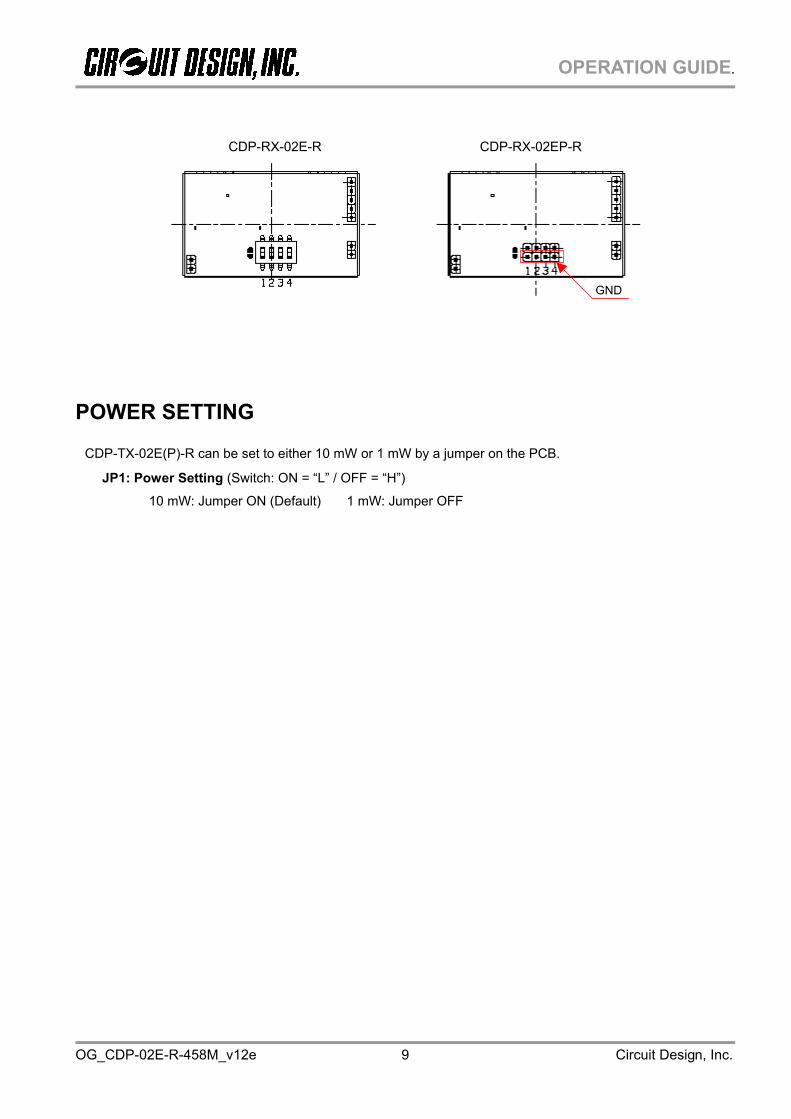
Position of the JP1 (power setting), DIP SW and Pins.
CDP-TX-02E-R CDP-TX-02EP-R
GND JP1
OPERATION GUIDE.
OG_CDP-02E-R-458M_v12e Circuit Design, Inc. 9
CDP-RX-02E-R CDP-RX-02EP-R
POWER SETTING
CDP-TX-02E(P)-R can be set to either 10 mW or 1 mW by a jumper on the PCB.
JP1: Power Setting (Switch: ON = “L” / OFF = “H”)
10 mW: Jumper ON (Default) 1 mW: Jumper OFF
GND
OPERATION GUIDE.
OG_CDP-02E-R-458M_v12e Circuit Design, Inc. 10
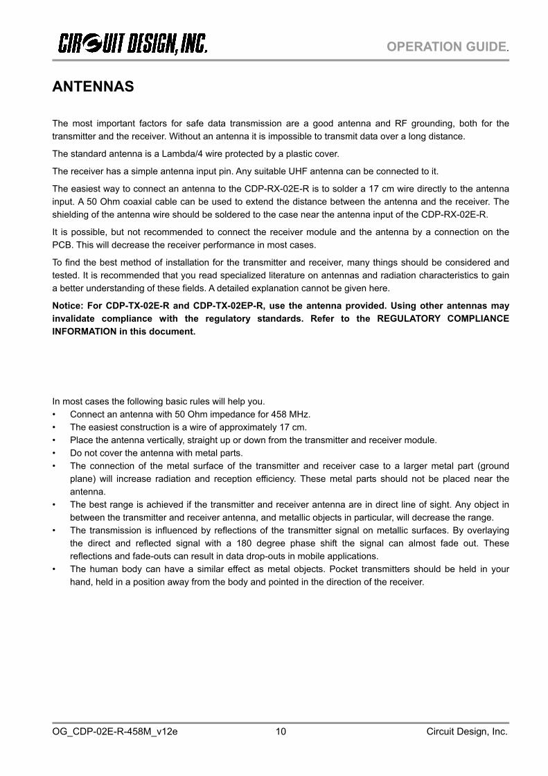
ANTENNAS The most important factors for safe data transmission are a good antenna and RF grounding, both for the transmitter and the receiver. Without an antenna it is impossible to transmit data over a long distance.
The standard antenna is a Lambda/4 wire protected by a plastic cover.
The receiver has a simple antenna input pin. Any suitable UHF antenna can be connected to it.
The easiest way to connect an antenna to the CDP-RX-02E-R is to solder a 17 cm wire directly to the antenna input. A 50 Ohm coaxial cable can be used to extend the distance between the antenna and the receiver. The shielding of the antenna wire should be soldered to the case near the antenna input of the CDP-RX-02E-R.
It is possible, but not recommended to connect the receiver module and the antenna by a connection on the PCB. This will decrease the receiver performance in most cases.
To find the best method of installation for the transmitter and receiver, many things should be considered and tested. It is recommended that you read specialized literature on antennas and radiation characteristics to gain a better understanding of these fields. A detailed explanation cannot be given here.
Notice: For CDP-TX-02E-R and CDP-TX-02EP-R, use the antenna provided. Using other antennas may invalidate compliance with the regulatory standards. Refer to the REGULATORY COMPLIANCE INFORMATION in this document.
In most cases the following basic rules will help you. • Connect an antenna with 50 Ohm impedance for 458 MHz. • The easiest construction is a wire of approximately 17 cm. • Place the antenna vertically, straight up or down from the transmitter and receiver module. • Do not cover the antenna with metal parts. • The connection of the metal surface of the transmitter and receiver case to a larger metal part (ground
plane) will increase radiation and reception efficiency. These metal parts should not be placed near the antenna.
• The best range is achieved if the transmitter and receiver antenna are in direct line of sight. Any object in between the transmitter and receiver antenna, and metallic objects in particular, will decrease the range.
• The transmission is influenced by reflections of the transmitter signal on metallic surfaces. By overlaying the direct and reflected signal with a 180 degree phase shift the signal can almost fade out. These reflections and fade-outs can result in data drop-outs in mobile applications.
• The human body can have a similar effect as metal objects. Pocket transmitters should be held in your hand, held in a position away from the body and pointed in the direction of the receiver.
OPERATION GUIDE.
OG_CDP-02E-R-458M_v12e Circuit Design, Inc. 11
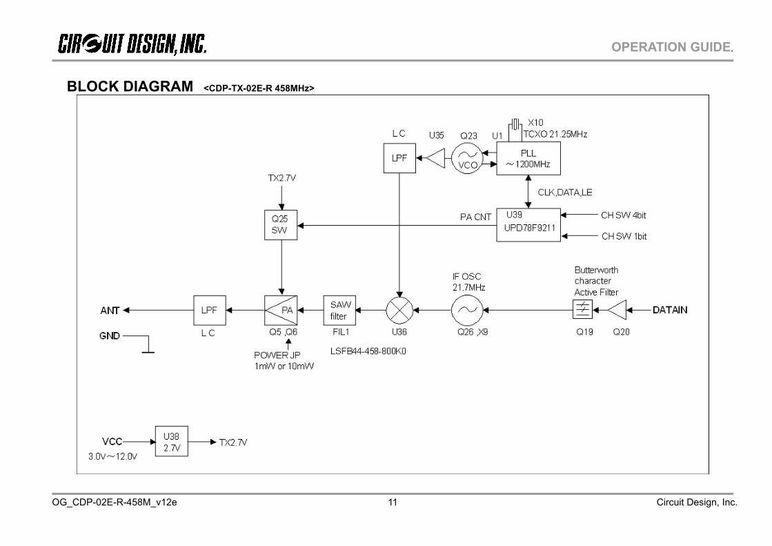
BLOCK DIAGRAM <CDP-TX-02E-R 458MHz>
OPERATION GUIDE.
OG_CDP-02E-R-458M_v12e Circuit Design, Inc. 12
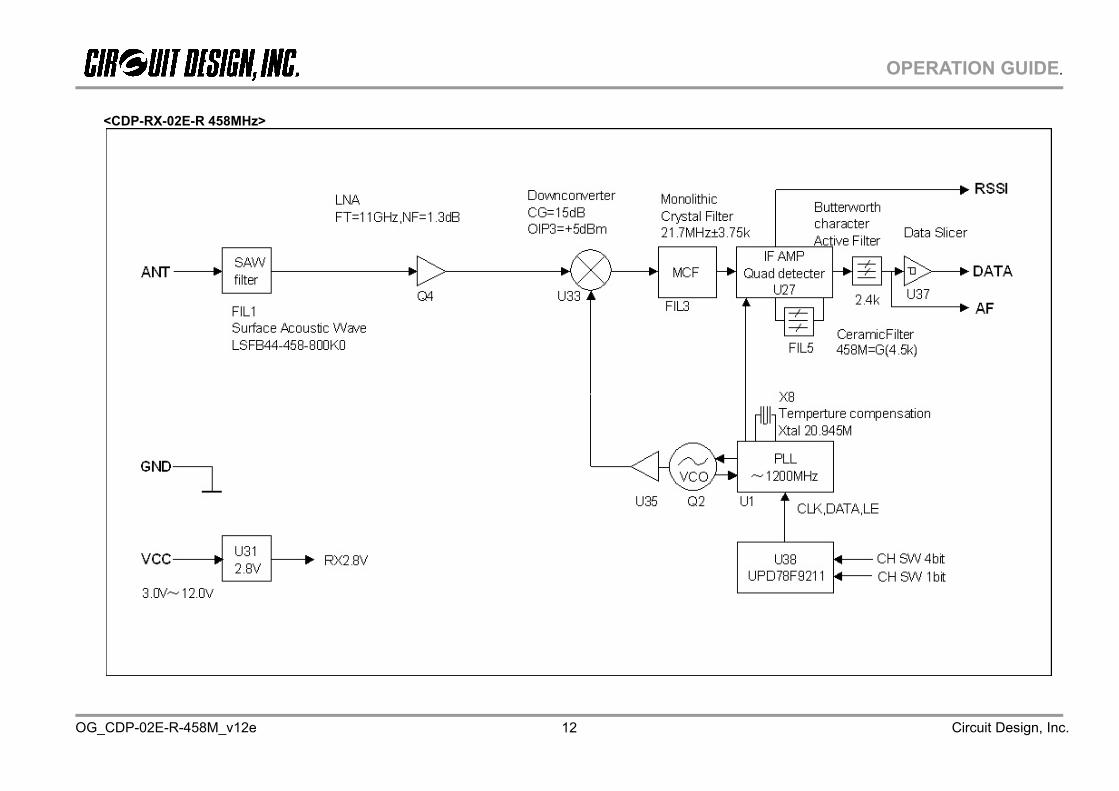
<CDP-RX-02E-R 458MHz>
OPERATION GUIDE.
OG_CDP-02E-R-458M_v12e Circuit Design, Inc. 13
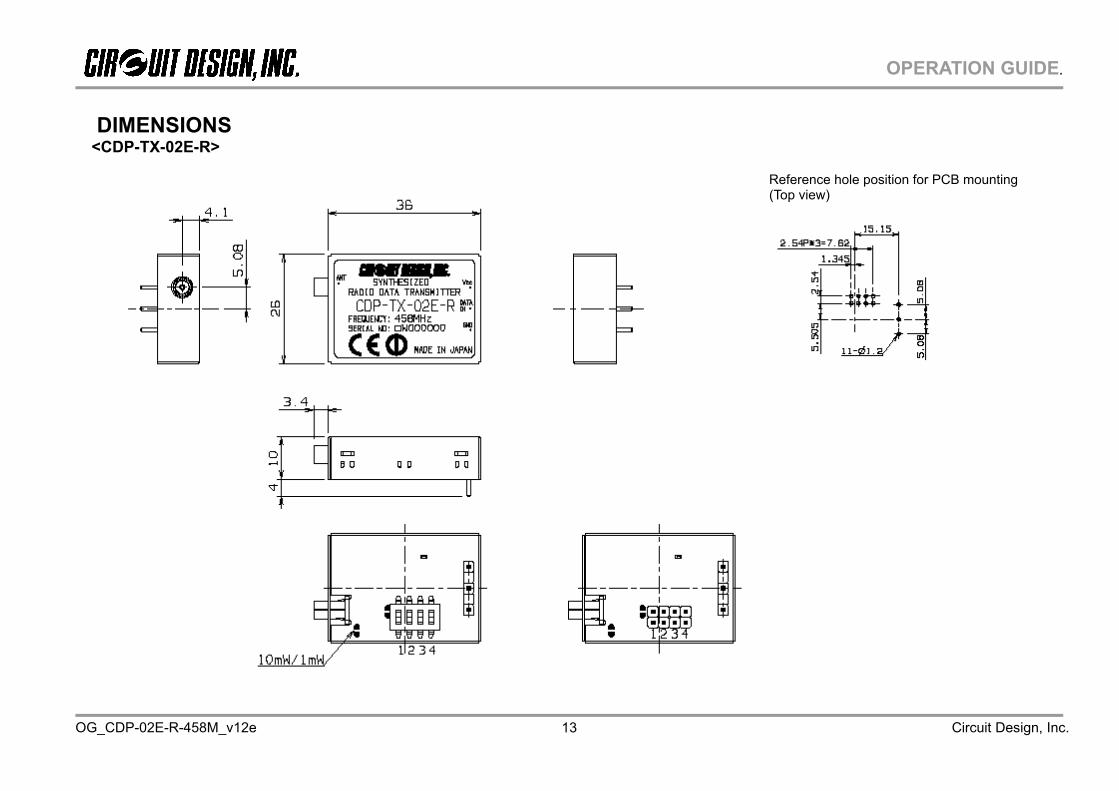
DIMENSIONS
<CDP-TX-02E-R>
Reference hole position for PCB mounting (Top view)
OPERATION GUIDE.
OG_CDP-02E-R-458M_v12e Circuit Design, Inc. 14
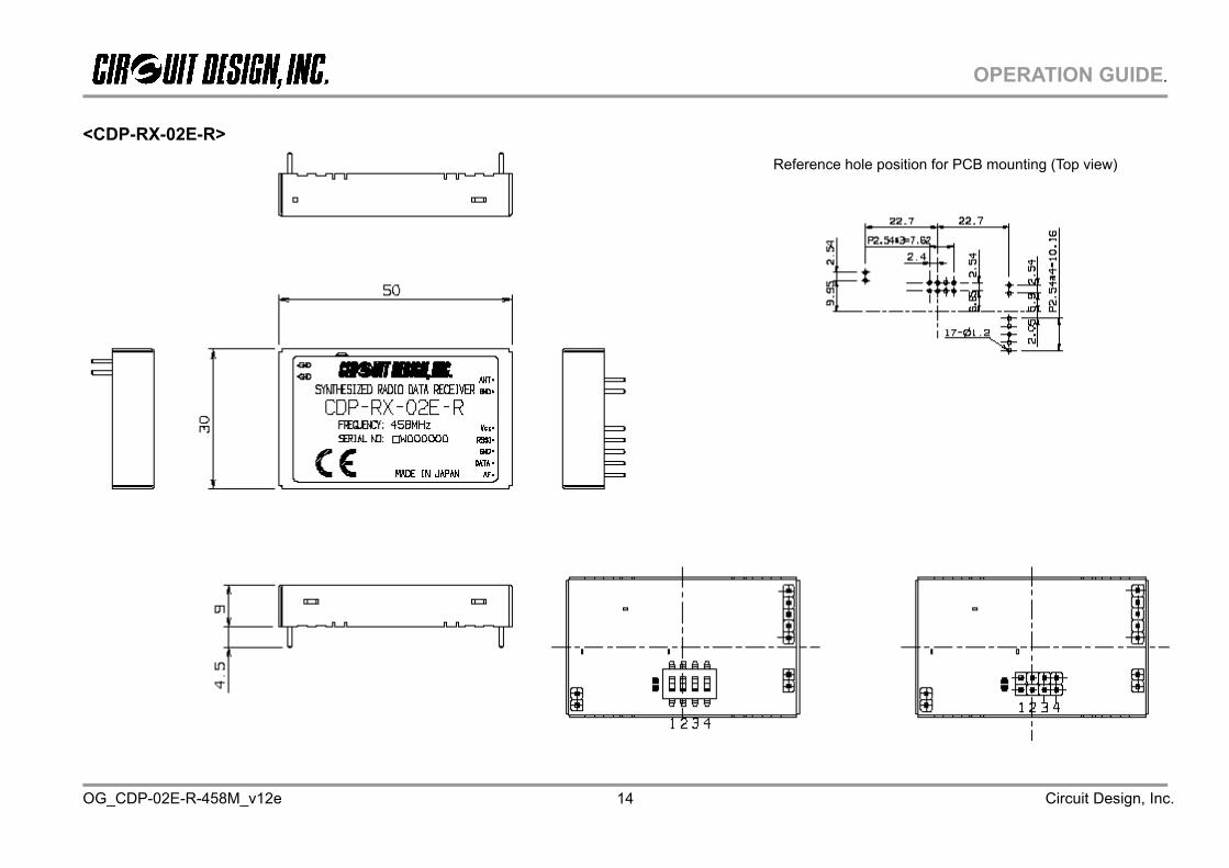
<CDP-RX-02E-R>
Reference hole position for PCB mounting (Top view)
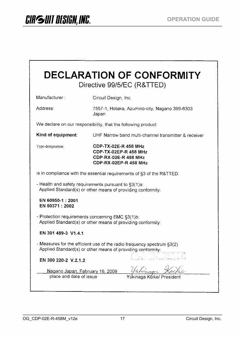
Regulatory compliance information Regulatory compliance of the CDP-TX-02E(P)-R and the CDP-RX-02E(P)-R the CDP-TX-02E(P)-R and the CDP-RX-02E(P)-R are designed for embedding in other equipment. (Products incorporating the CDP-TX-02E(P)-R and the CDP-RX-02E(P)-R are henceforward referred to as final products.) The European regulation applicable to the CDP-TX-02E(P)-R and the CDP-RX-02E(P)-R is the R&TTE Directive 1999/5/EC.The conformity assessment for the CDP-TX-02E(P)-R and the CDP-RX-02E(P)-R was completed in accordance with the R&TTE Directive Annex II (RX) and III (TX) procedures, and the Declaration of Conformity is attached to this manual. The CDP-TX-02E(P)-R 458MHz and the CDP-RX-02E(P)-R 458MHz are designed to be used in the 458MHz band allocated for Industrial or commercial telemetry and telecommand devices in UK. The applicable technical specification is EN 300 220. Cautions related to regulatory compliance when embedding the CDP-TX-02E(P)-R and the CDP-RX-02E(P)-R.
1. Antenna The CDP-TX-02E(P)-R is supplied with a dedicated antenna and the conformity assessment of the CDP-TX-02E(P)-R was performed using the dedicated antenna (Circuit Design’s standard antenna ANT-LEA-01, 1/4 lambda lead antenna). If you use an antenna other than the dedicated anntena or an antenna with equivalent characteristics and performance, further radio conformity assessment may be required. 2. Duty cycle The CDP-TX-02E(P)-R 458MHz continuously emits carrier signals when power is supplied. The user must design the final product to meet the requirements of the duty cycle as provided in the relevant regulations. 3. Supply voltage The CDP-TX-02E(P)-R should be used within the specified voltage range (3.0 V to 12 V). 4. Enclosure To fulfill the requirements of EMC and safety requirements, the CDP-TX-02E(P)-R and the CDP-RX-02E(P)-R should be mounted on the circuit boards of the final products and must be enclosed in the cases of the final products. No surface of the CDP-TX-02E(P)-R and the CDP-RX-02E(P)-R should be exposed.
Conformity assessment of the final product The manufacturer of the final product is responsible for the conformity assessment procedures of the final product in accordance with the R&TTE Directive. As to the conformity assessment of the R&TTE Directive Article 3.2 (Efficient use of the radio spectrum), the manufacturer of the final product incorporating the R&TTE assessed CDP-TX-02E(P)-R and CDP-RX-02E(P)-R will be exempted from its conformity assessment procedures. For details of how to use the conformity assessment of the CDP-TX-02E(P)-R and the CDP-RX-02E(P)-R, please consult the relevant authorities or accredited certification bodies. Notification of the final product The notification required by R&TTE Directive Article 6 (4) is not necessary if the final product is used in the harmonized frequency band and is classified as Class-1 equipment. If the final product is not used in the harmonized frequency band and is classified as Class-2 equipment, the manufacturer of the final product has a duty to notify the relevant radio regulatory authorities in the countries where the final product is sold. * A list of Class-1 equipment is available at http://www.ero.dk/. Exemption clause Circuit Design, Inc does not guarantee the accuracy of the above mentioned information about the conformity assessment and notification of the final product. Directives, technical standards, principles of operation and the like may be interpreted differently by the authorities in each country. Also the national laws and restrictions vary with the country. In case of doubt or uncertainty, we recommend that you check with the authorities or official certification organizations of the relevant countries.
OG_CDP-02E-R-458M_v12e Circuit Design, Inc. 17
OPERATION GUIDE
OG_CDP-02E-R-458M_v12e Circuit Design, Inc. 18
OPERATION GUIDE
Important notice • Customers are advised to consult with Circuit Design sales representatives before ordering.
Circuit Design believes the provided information is accurate and reliable. However, Circuit Design reserves the right to make changes to this product without notice.
• Circuit Design products are neither designed nor intended for use in life support applications where
malfunction can reasonably be expected to result in significant personal injury to the user. Any use of Circuit Design products in such safety-critical applications is understood to be fully at the risk of the customer and the customer must fully indemnify Circuit Design, Inc for any damages resulting from any improper use.
• As the radio module communicates using electronic radio waves, there are cases where transmission will be temporarily cut off due to the surrounding environment and method of usage. The manufacturer is exempt from all responsibility relating to resulting harm to personnel or equipment and other secondary damage.
• The manufacturer is exempt from all responsibility relating to secondary damage resulting from the operation, performance and reliability of equipment connected to the radio module.
Copyright • All rights in this operation guide are owned by Circuit Design, Inc. No part of this document may be copied
or distributed in part or in whole without the prior written consent of Circuit Design, Inc.
Cautions • Do not use the equipment within the vicinity of devices that may malfunction as a result of electronic radio
waves from the radio module. • Communication performance will be affected by the surrounding environment, so communication tests should
be carried out before actual use. • Ensure that the power supply for the radio module is within the specified rating. Short circuits and reverse
connections may result in overheating and damage and must be avoided at all costs. • Ensure that the power supply has been switched off before attempting any wiring work. • The case is connected to the GND terminal of the internal circuit, so do not make contact between the '+' side
of the power supply terminal and the case. • When batteries are used as the power source, avoid short circuits, recharging, dismantling, and pressure.
Failure to observe this caution may result in the outbreak of fire, overheating and damage to the equipment. Remove the batteries when the equipment is not to be used for a long period of time. Failure to observe this caution may result in battery leaks and damage to the equipment.
• Do not use this equipment in vehicles with the windows closed, in locations where it is subject to direct sunlight, or in locations with extremely high humidity.
• The radio module is neither waterproof nor splash proof. Ensure that it is not splashed with soot or water. Do not use the equipment if water or other foreign matter has entered the case.
• Do not drop the radio module or otherwise subject it to strong shocks. • Do not subject the equipment to condensation (including moving it from cold locations to locations with a
significant increase in temperature.) • Do not use the equipment in locations where it is likely to be affected by acid, alkalis, organic agents or
corrosive gas. • Do not bend or break the antenna. Metallic objects placed in the vicinity of the antenna will have a great
effect on communication performance. As far as possible, ensure that the equipment is placed well away from metallic objects.
• The GND for the radio module will also affect communication performance. If possible, ensure that the case GND and the circuit GND are connected to a large GND pattern.
Warnings • Do not take a part or modify the equipment. • Do not remove the product label (the label attached to the upper surface of the module.) Using a module from
which the label has been removed is prohibited. Copyright 2009, Circuit Design, Inc.
OG_CDP-02E-R-458M_v12e Circuit Design, Inc. 19
OPERATION GUIDE
REVISION HISTORY Version Date Description Remark 1.0 Jul. 2006 CDP-TX/RX-02E-R 458MHz The first issue 1.1 Mar. 2008 DOC updated Page 17 1.2 Feb. 2009 DOC updated, Important notice added Page 17 & 18
OG_CDP-02E-R-458M_v12e Circuit Design, Inc. 20
OPERATION GUIDE
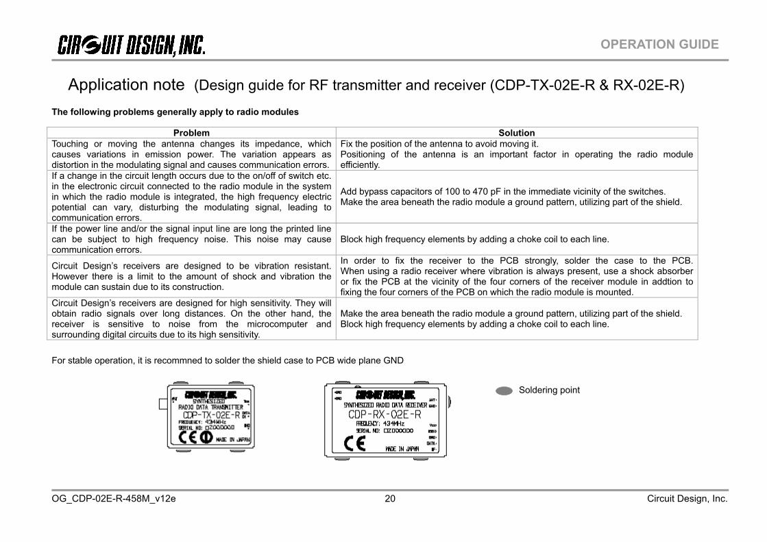
Application note (Design guide for RF transmitter and receiver (CDP-TX-02E-R & RX-02E-R)
The following problems generally apply to radio modules
For stable operation, it is recommned to solder the shield case to PCB wide plane GND
Problem Solution Touching or moving the antenna changes its impedance, which causes variations in emission power. The variation appears as distortion in the modulating signal and causes communication errors.
Fix the position of the antenna to avoid moving it. Positioning of the antenna is an important factor in operating the radio module efficiently.
If a change in the circuit length occurs due to the on/off of switch etc. in the electronic circuit connected to the radio module in the system in which the radio module is integrated, the high frequency electric potential can vary, disturbing the modulating signal, leading to communication errors.
Add bypass capacitors of 100 to 470 pF in the immediate vicinity of the switches. Make the area beneath the radio module a ground pattern, utilizing part of the shield.
If the power line and/or the signal input line are long the printed line can be subject to high frequency noise. This noise may cause communication errors.
Block high frequency elements by adding a choke coil to each line.
Circuit Design’s receivers are designed to be vibration resistant. However there is a limit to the amount of shock and vibration the module can sustain due to its construction.
In order to fix the receiver to the PCB strongly, solder the case to the PCB. When using a radio receiver where vibration is always present, use a shock absorber or fix the PCB at the vicinity of the four corners of the receiver module in addtion to fixing the four corners of the PCB on which the radio module is mounted.
Circuit Design’s receivers are designed for high sensitivity. They will obtain radio signals over long distances. On the other hand, the receiver is sensitive to noise from the microcomputer and surrounding digital circuits due to its high sensitivity.
Make the area beneath the radio module a ground pattern, utilizing part of the shield. Block high frequency elements by adding a choke coil to each line.
Soldering point
OG_CDP-02E-R-458M_v12e Circuit Design, Inc. 21
OPERATION GUIDE
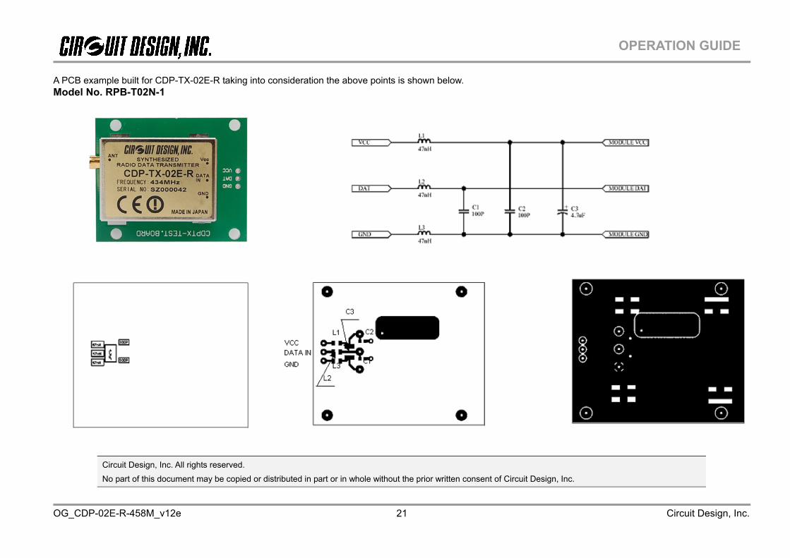
A PCB example built for CDP-TX-02E-R taking into consideration the above points is shown below. Model No. RPB-T02N-1
Circuit Design, Inc. All rights reserved.
No part of this document may be copied or distributed in part or in whole without the prior written consent of Circuit Design, Inc.