Kevin Zhou 1/1301- BMR 453 Uen Approved Checked Date Rev Reference
Kevin Zhou 2017-09-22 S
Key Features • Industry standard five pin Quarter-brick
57.9 x 36.8 x 11.6 mm (2.28 x 1.45 x 0.46 in.) • Optional digital PMBus interface • Fully regulated intermediate bus converter • High efficiency, typ. 96% at half load, 12 Vout • +/- 2% output voltage tolerance band • 1500 Vdc input to output isolation • 2.5 million hours MTBF • Optional baseplate • Optional output voltage Droop for parallel operation • ISO 9001/14001 certified supplier • PMBus Revision 1.1 compliant Power Management • Configurable soft start/stop • Precision delay and ramp-up • Voltage sequencing and margining • Voltage/current/temperature monitoring • Configurable output voltage • Power good • Synchronization • Voltage track
Safety Approvals Design for Environment
Meets requirements in high-temperature lead-free soldering processes.
Ericsson Internal TABLE OF CONTENTS 1 (1)
Prepared (also subject responsible if other) No.
SEC/S Kevin Zhou 00152-EN/LZT146395 Approved Checked Date Rev Reference
SEC/S Kevin Zhou 2011-07-07 J
Contents
Ordering Information ............................................................. 2 General Information ............................................................. 2 Safety Specification ............................................................. 4 Absolute Maximum Ratings ............................................................. 5 Functional Description ............................................................. 6 Electrical Specification 3.3 V, 60 A / 198 W BMR 453 0002/003 ............................... 7 5 V, 60 A / 300 W BMR 453 0002/004 ............................. 10 9 V, 33 A / 297 W BMR 453 0000/002 ............................. 13 12 V, 33 A / 396 W BMR 453 0000/001 ............................. 16 EMC Specification ........................................................... 19 Operating Information ........................................................... 20 Thermal considerations ........................................................... 23 Connections ........................................................... 24 PMBus communications ........................................................... 25 Mechanical Information ........................................................... 28 Soldering Information ........................................................... 32 Delivery Information ........................................................... 33 Product Qualification Specification ........................................................... 35
BMR453 series Fully regulated Advanced Bus ConvertersInput 36-75 V, Output up to 60 A / 396 W
Kevin Zhou 1/1301- BMR 453 Uen Approved Checked Date Rev Reference
Kevin Zhou 2017-09-22 S
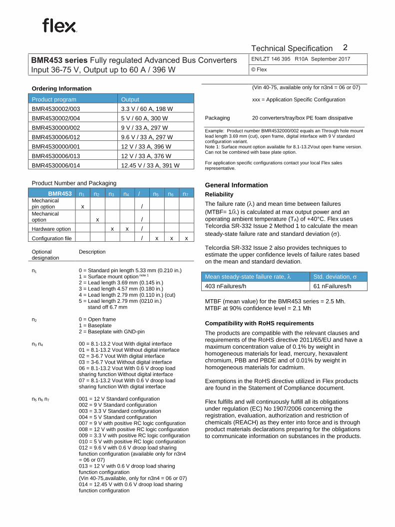
Ordering Information
Product program Output
BMR4530002/003 3.3 V / 60 A, 198 W
BMR4530002/004 5 V / 60 A, 300 W
BMR4530000/002 9 V / 33 A, 297 W
BMR4530006/012 9.6 V / 33 A, 297 W
BMR4530000/001 12 V / 33 A, 396 W
BMR4530006/013 12 V / 33 A, 376 W
BMR4530006/014 12.45 V / 33 A, 391 W
Product Number and Packaging
BMR453 n1 n2 n3 n4 / n5 n6 n7 Mechanical pin option x / Mechanical option x /
Hardware option x x /
Configuration file / x x x Optional designation
Description
n1
n2
n3 n4
n5 n6 n7
0 = Standard pin length 5.33 mm (0.210 in.) 1 = Surface mount option note 1 2 = Lead length 3.69 mm (0.145 in.) 3 = Lead length 4.57 mm (0.180 in.) 4 = Lead length 2.79 mm (0.110 in.) (cut) 5 = Lead length 2.79 mm (0210 in.) stand off 6.7 mm 0 = Open frame 1 = Baseplate 2 = Baseplate with GND-pin 00 = 8.1-13.2 Vout With digital interface 01 = 8.1-13.2 Vout Without digital interface 02 = 3-6.7 Vout With digital interface 03 = 3-6.7 Vout Without digital interface 06 = 8.1-13.2 Vout With 0.6 V droop load sharing function Without digital interface 07 = 8.1-13.2 Vout With 0.6 V droop load sharing function With digital interface 001 = 12 V Standard configuration 002 = 9 V Standard configuration 003 = 3.3 V Standard configuration 004 = 5 V Standard configuration 007 = 9 V with positive RC logic configuration 008 = 12 V with positive RC logic configuration 009 = 3.3 V with positive RC logic configuration 010 = 5 V with positive RC logic configuration 012 = 9.6 V with 0.6 V droop load sharing function configuration (available only for n3n4 = 06 or 07) 013 = 12 V with 0.6 V droop load sharing function configuration (Vin 40-75,available, only for n3n4 = 06 or 07) 014 = 12.45 V with 0.6 V droop load sharing function configuration
Packaging
(Vin 40-75, available only for n3n4 = 06 or 07) xxx = Application Specific Configuration 20 converters/tray/box PE foam dissipative
Example: Product number BMR4532000/002 equals an Through hole mount lead length 3.69 mm (cut), open frame, digital interface with 9 V standard configuration variant. Note 1: Surface mount option available for 8.1-13.2Vout open frame version. Can not be combined with base plate option. For application specific configurations contact your local Flex sales representative.
General Information Reliability
The failure rate () and mean time between failures (MTBF= 1/) is calculated at max output power and an operating ambient temperature (TA) of +40°C. Flex uses Telcordia SR-332 Issue 2 Method 1 to calculate the mean steady-state failure rate and standard deviation (). Telcordia SR-332 Issue 2 also provides techniques to estimate the upper confidence levels of failure rates based on the mean and standard deviation. Mean steady-state failure rate, Std. deviation,
403 nFailures/h 61 nFailures/h MTBF (mean value) for the BMR453 series = 2.5 Mh. MTBF at 90% confidence level = 2.1 Mh
Compatibility with RoHS requirements
The products are compatible with the relevant clauses and requirements of the RoHS directive 2011/65/EU and have a maximum concentration value of 0.1% by weight in homogeneous materials for lead, mercury, hexavalent chromium, PBB and PBDE and of 0.01% by weight in homogeneous materials for cadmium. Exemptions in the RoHS directive utilized in Flex products are found in the Statement of Compliance document. Flex fulfills and will continuously fulfill all its obligations under regulation (EC) No 1907/2006 concerning the registration, evaluation, authorization and restriction of chemicals (REACH) as they enter into force and is through product materials declarations preparing for the obligations to communicate information on substances in the products.
BMR453 series Fully regulated Advanced Bus ConvertersInput 36-75 V, Output up to 60 A / 396 W
Kevin Zhou 1/1301- BMR 453 Uen Approved Checked Date Rev Reference
Kevin Zhou 2017-09-22 S
Quality Statement
The products are designed and manufactured in an industrial environment where quality systems and methods like ISO 9000, Six Sigma, and SPC are intensively in use to boost the continuous improvements strategy. Infant mortality or early failures in the products are screened out and they are subjected to an ATE-based final test. Conservative design rules, design reviews and product qualifications, plus the high competence of an engaged work force, contribute to the high quality of the products. Warranty
Warranty period and conditions are defined in Flex General Terms and Conditions of Sale. Limitation of Liability
The information and specifications in this technical specification is believed to be correct at the time of publication. However, no liability is accepted for inaccuracies, printing errors or for any consequences thereof. Flex reserves the right to change the contents of this technical specification at any time without prior notice.
BMR453 series Fully regulated Advanced Bus ConvertersInput 36-75 V, Output up to 60 A / 396 W
Kevin Zhou 1/1301- BMR 453 Uen Approved Checked Date Rev Reference
Kevin Zhou 2017-09-22 S
Safety Specification
General information
Flex DC/DC converters and DC/DC regulators are designed in accordance with the safety standards IEC 60950-1, EN 60950-1 and UL 60950-1 Safety of Information Technology Equipment. IEC/EN/UL 60950-1 contains requirements to prevent injury or damage due to the following hazards:
• Electrical shock • Energy hazards • Fire • Mechanical and heat hazards • Radiation hazards • Chemical hazards
On-board DC/DC converters and DC/DC regulators are defined as component power supplies. As components they cannot fully comply with the provisions of any safety requirements without “conditions of acceptability”. Clearance between conductors and between conductive parts of the component power supply and conductors on the board in the final product must meet the applicable safety requirements. Certain conditions of acceptability apply for component power supplies with limited stand-off (see Mechanical Information and Safety Certificate for further information). It is the responsibility of the installer to ensure that the final product housing these components complies with the requirements of all applicable safety standards and regulations for the final product. Component power supplies for general use should comply with the requirements in IEC/EN/UL 60950-1 Safety of Information Technology Equipment. Product related standards, e.g. IEEE 802.3af Power over Ethernet, and ETS-300132-2 Power interface at the input to telecom equipment, operated by direct current (dc) are based on IEC/EN/UL 60950-1 with regards to safety. Flex DC/DC converters, Power interface modules and DC/DC regulators are UL 60950-1 recognized and certified in accordance with EN 60950-1. The flammability rating for all construction parts of the products meet requirements for V-0 class material according to IEC 60695-11-10, Fire hazard testing, test flames – 50 W horizontal and vertical flame test methods. Isolated DC/DC converters & Power interface modules
The product may provide basic or functional insulation between input and output according to IEC/EN/UL 60950-1 (see Safety Certificate), different conditions shall be met if the output of a basic or a functional insulated product shall be considered as safety extra low voltage (SELV). For basic insulated products (see Safety Certificate) the
output is considered as safety extra low voltage (SELV) if one of the following conditions is met:
• The input source provides supplementary or double or reinforced insulation from the AC mains according to IEC/EN/UL 60950-1.
• The input source provides functional or basic insulation from the AC mains and the product’s output is reliably connected to protective earth according to IEC/EN/UL 60950-1.
For functional insulated products (see Safety Certificate) the output is considered as safety extra low voltage (SELV) if one of the following conditions is met:
• The input source provides double or reinforced insulation from the AC mains according to IEC/EN/UL 60950-1.
• The input source provides basic or supplementary insulation from the AC mains and the product’s output is reliably connected to protective earth according to IEC/EN/UL 60950-1.
• The input source is reliably connected to protective earth and provides basic or supplementary insulation according to IEC/EN/UL 60950-1 and the maximum input source voltage is 60 Vdc.
Galvanic isolation between input and output is verified in an electric strength test and the isolation voltage (Viso) meets the voltage strength requirement for basic insulation according to IEC/EN/UL 60950-1. It is recommended to use a slow blow fuse at the input of each DC/DC converter. If an input filter is used in the circuit the fuse should be placed in front of the input filter. In the rare event of a component problem that imposes a short circuit on the input source, this fuse will provide the following functions:
• Isolate the fault from the input power source so as not to affect the operation of other parts of the system
• Protect the distribution wiring from excessive current and power loss thus preventing hazardous overheating
Non - isolated DC/DC regulators The DC/DC regulator output is SELV if the input source meets the requirements for SELV circuits according to IEC/EN/UL 60950-1.
BMR453 series Fully regulated Advanced Bus ConvertersInput 36-75 V, Output up to 60 A / 396 W
TP1 Operating Temperature (see Thermal Consideration section) -40 +125 °C
TS Storage temperature -55 +125 °C
VI Input voltage -0.5 80 V
Viso Isolation voltage (input to output test voltage), see note 1 1500 Vdc
Vtr Input voltage transient (Tp 100 ms) 100 V
VRC Remote Control pin voltage -0.3 18 V
V Logic I/O SALERT, CTRL, SYNC, SCL, SDA, SA(0,1) -0.3 3.6 V
Stress in excess of Absolute Maximum Ratings may cause permanent damage. Absolute Maximum Ratings, sometimes ref erred to as no destruction limits, are normally tested with one parameter at a time exceeding the limits of Output data or Electrical Characteristics. If exposed to stress abov e these limits, f unction and perf ormance may degrade in an unspecif ied manner. Note 1: Isolation v oltage (input/output to base-plate) max 750 Vdc.
Fundamental Circuit Diagram
-IN
+IN
+OUT
-OUT
Driver
Driv
er
Control
RC isolation
AuxillarySupply
RC
BMR453 series Fully regulated Advanced Bus ConvertersInput 36-75 V, Output up to 60 A / 396 W
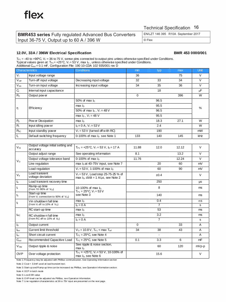
TP1 = -40 to +90ºC, VI = 36 to 75 V, sense pins connected to output pins unless otherwise specif ied under Conditions. Typical values given at: TP1 = +25°C, VI= 53 V, max IO , unless otherwise specif ied under Conditions Configuration File: 190 10-CDA 102 935/001 rev D
Characteristics Conditions min typ max Unit
PMBus monitoring accuracy
VIN_READ Input voltage -3 +0.4 3 %
VOUT_READ Output voltage VI = 53 V -1.0 -0.3 1.0 %
IOUT_READ Output current VI = 53 V, 50-100% of max IO -6 ±1 6 %
IOUT_READ Output current VI = 53 V, 10% of max IO -0.7 - 0.7 A
TEMP_READ Temperature -5 - 5 ºC
Fault Protection Characteristics
Input Under Voltage Lockout, UVLO
Factory default - 33 - V
Setpoint accuracy -3 - 3 %
Hysteresis Factory default - 1.8 - V
Configurable via PMBus of threshold range, Note 1 0 - - V
Delay - 200 - μs
(Output voltage) Over/Under Voltage Protection, OVP/UVP
Logic output high (VOH) CTRL_CS, PG_SYNC, SALERT, SCL, SDA IOH = -5 mA
2.8 - - V
Setup time, SMBus 100 - ns
Hold time, SMBus 300 - ns
Bus free time T(BUF) Note 2 200 - us
Note 1: See Operating Infor mation section.
Note 2: It is recommended that a PMBus mas ter read back written data for verification i.e. do not r ely on the ACK/NACK bit since this bit are as susceptibl e to errors as any other bit*. However, under ver y rare operating conditi ons, it is possible to get intermittent r ead back failures. I t is therefore recommended to i mplement error handling in the master that also deals with those situations.
BMR453 series Fully regulated Advanced Bus ConvertersInput 36-75 V, Output up to 60 A / 396 W
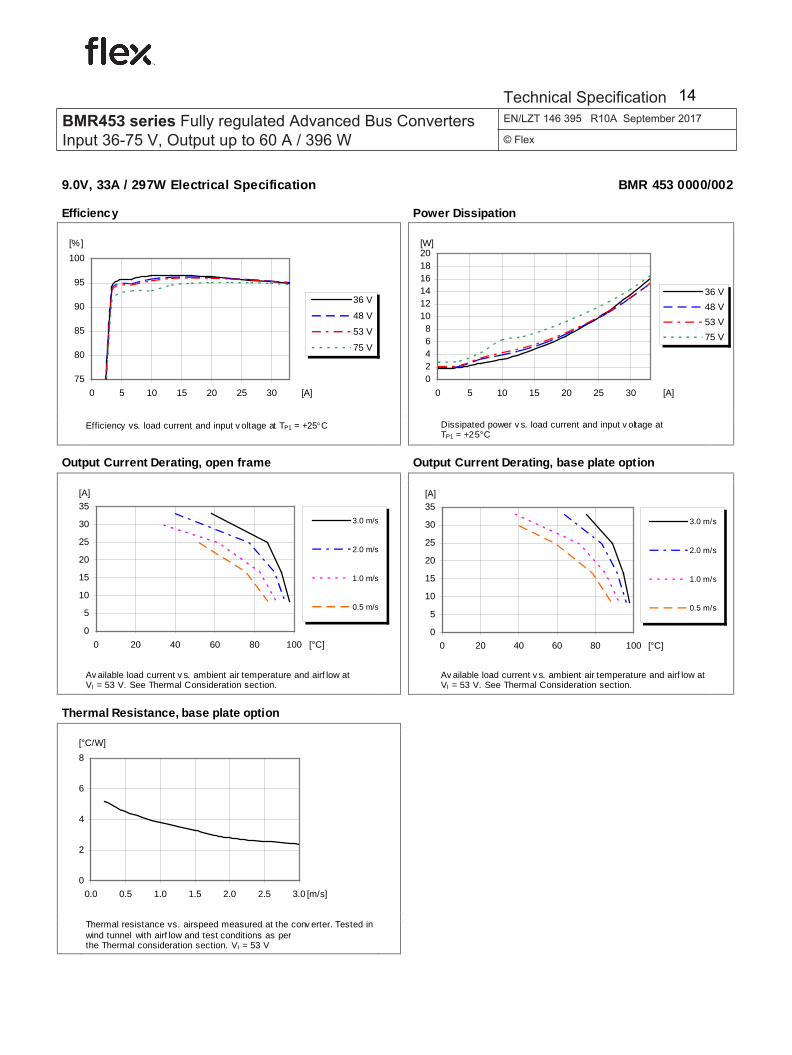
Efficiency vs. load current and input v oltage at TP1 = +25°C Dissipated power v s. load current and input v oltage at TP1 = +25°C
Output Current Derating, open frame Output Current Derating, base plate option
0
10
20
30
40
50
60
10 30 50 70 90 110 [°C]
[A]
3.0 m/s
2.0 m/s
1.0 m/s
0.5 m/s
0
10
20
30
40
50
60
10 30 50 70 90 110 [°C]
[A]
3.0 m/s
2.0 m/s
1.0 m/s
0.5 m/s
Av ailable load current v s. ambient air temperature and airf low at VI = 53 V. See Thermal Consideration section.
Av ailable load current v s. ambient air temperature and airf low at VI = 53 V. See Thermal Consideration section.
Thermal Resistance, base plate option
0
2
4
6
8
0,0 0,5 1,0 1,5 2,0 2,5 3,0[m/s]
[°C/W]
Thermal resistance vs. airspeed measured at the conv erter. Tested in wind tunnel with airf low and test conditions as per the Thermal consideration section. VI = 53 V
BMR453 series Fully regulated Advanced Bus ConvertersInput 36-75 V, Output up to 60 A / 396 W
Efficiency vs. load current and input v oltage at TP1 = +25°C Dissipated power v s. load current and input v oltage at TP1 = +25°C
Output Current Derating, open frame Output Current Derating, base plate option
0
10
20
30
40
50
60
10 30 50 70 90 110 [°C]
[A]
3.0 m/s
2.0 m/s
1.0 m/s
0.5 m/s
0
10
20
30
40
50
60
10 30 50 70 90 110 [°C]
[A]
3.0 m/s
2.0 m/s
1.0 m/s
0.5 m/s
Av ailable load current v s. ambient air temperature and airf low at VI = 53 V. See Thermal Consideration section.
Av ailable load current v s. ambient air temperature and airf low at VI = 53 V. See Thermal Consideration section.
Thermal Resistance, base plate option
0
2
4
6
8
0.0 0.5 1.0 1.5 2.0 2.5 3.0 [m/s]
[°C/W]
Thermal resistance vs. airspeed measured at the conv erter. Tested in wind tunnel with airf low and test conditions as per the Thermal consideration section. VI = 53 V
BMR453 series Fully regulated Advanced Bus ConvertersInput 36-75 V, Output up to 60 A / 396 W
Efficiency vs. load current and input v oltage at TP1 = +25°C Dissipated power v s. load current and input v oltage at TP1 = +25°C
Output Current Derating, open frame Output Current Derating, base plate option
0
5
10
15
20
25
30
35
0 20 40 60 80 100 [°C]
[A]
3.0 m/s
2.0 m/s
1.0 m/s
0.5 m/s
0
5
10
15
20
25
30
35
0 20 40 60 80 100 [°C]
[A]
3.0 m/s
2.0 m/s
1.0 m/s
0.5 m/s
Av ailable load current v s. ambient air temperature and airf low at VI = 53 V. See Thermal Consideration section.
Av ailable load current v s. ambient air temperature and airf low at VI = 53 V. See Thermal Consideration section.
Thermal Resistance, base plate option
0
2
4
6
8
0.0 0.5 1.0 1.5 2.0 2.5 3.0 [m/s]
[°C/W]
Thermal resistance vs. airspeed measured at the conv erter. Tested in wind tunnel with airf low and test conditions as per the Thermal consideration section. VI = 53 V
BMR453 series Fully regulated Advanced Bus ConvertersInput 36-75 V, Output up to 60 A / 396 W
VOac Output ripple & noise See ripple & noise section, max IO
60 120 mVp-p
OVP Over voltage protection TP1 = +25°C, VI = 53 V, 10-100% of max IO, see Note 6
15.6 V
Note 1: Frequency may be adj usted with PMBus communication. See Operating Information sec tion
Note 2: Cout = 3.3mF used at l oad transient tes t.
Note 3: Start-up and R amp-up time can be increased via PMBus, see Operation Information section.
Note 4: OCP in latch mode
Note 5: Low ESR-value
Note 6: OVP-level can be adj usted via PMBus, see Operati on Information. Note 7: Li ne r egulation characteristics at 36 to 75V input are presented on the next page.
BMR453 series Fully regulated Advanced Bus ConvertersInput 36-75 V, Output up to 60 A / 396 W
Efficiency vs. load current and input v oltage at TP1 = +25°C Dissipated power v s. load current and input v oltage at
TP1 = +25°C
Output Current Derating, open frame Output Current Derating, base plate option
0
5
10
15
20
25
30
35
0 20 40 60 80 100 [°C]
[A]
3.0 m/s
2.0 m/s
1.0 m/s
0.5 m/s
0
5
10
15
20
25
30
35
0 20 40 60 80 100 [°C]
[A]
3.0 m/s
2.0 m/s
1.0 m/s
0.5 m/s
Av ailable load current v s. ambient air temperature and airf low at VI = 53 V. See Thermal Consideration section.
Av ailable load current v s. ambient air temperature and airf low at VI = 53 V. See Thermal Consideration section.
Thermal Resistance, base plate option
0
2
4
6
8
0.0 0.5 1.0 1.5 2.0 2.5 3.0[m/s]
[°C/W]
Thermal resistance vs. airspeed measured at the conv erter. Tested in wind tunnel with airf low and test conditions as per the Thermal consideration section. VI = 53 V, IO = 25 A
BMR453 series Fully regulated Advanced Bus ConvertersInput 36-75 V, Output up to 60 A / 396 W
SECSUND 30/1301-BMR 453 Uen Approved Checked Date Rev Reference
BNEWIHCLB (Lisa Li) 2017-09-27 N
EMC Specification
Conducted EMI measured according to EN55022, CISPR 22 and FCC part 15J (see test set-up). See Design Note 009 for further information. The fundamental switching frequency is 140 kHz for BMR 453 @ VI = 53 V, max IO.
Conducted EMI Input terminal value (typ)
EMI without filter
External filter (class B) Suggested external input filter in order to meet class B in EN 55022, CISPR 22 and FCC part 15J.
Layout recommendation The radiated EMI performance of the product will depend on the PWB layout and ground layer design. It is also important to consider the stand-off of the product. If a ground layer is used, it should be connected to one of the output terminals and the equipment ground or chassis. A ground layer will increase the stray capacitance in the PWB and improve the high frequency EMC performance. Output ripple and noise Output ripple and noise measured according to figure below. See Design Note 022 for detailed information.
Output ripple and noise test setup
BMR453 series Fully regulated Advanced Bus ConvertersInput 36-75 V, Output up to 60 A / 396 W
SECSUND 30/1301-BMR 453 Uen Approved Checked Date Rev Reference
BNEWIHCLB (Lisa Li) 2017-09-27 N
Operating information Input Voltage The input voltage range 36 to 75 Vdc meets the requirements of the European Telecom Standard ETS 300 132-2 for normal input voltage range in -48 and -60 Vdc systems, -40.5 to -57.0 V and –50.0 to -72 V respectively. At input voltages exceeding 75 V, the power loss will be higher than at normal input voltage and TP1 must be limited to absolute max +125°C. The absolute maximum continuous input voltage is 80 Vdc. Turn-off Input Voltage The product monitors the input voltage and will turn on and turn off at predetermined levels. The turn on and turn off level and the hysteresis in between can be configured via the PMBus. The default hysteresis between turn on and turn off input voltage is set to 2 V. Remote Control (RC)
The products are fitted with a configurable remote control function. The primary remote control is referenced to the primary negative input connection (-In). The RC function allows the converter to be turned on/off by an external device like a semiconductor or mechanical switch. The RC pin has an internal pull up resistor. The remote control functions can also be configured using the PMBus.
The device should be capable of sinking 0.7 mA. When the RC pin is left open, the voltage generated on the RC pin is max 6 V. The standard product is provided with “negative logic” remote control and will be off until the RC pin is connected to the -In. To turn on the product the voltage between RC pin and -In should be less than 1 V. To turn off the product the RC pin should be left open. In situations where it is desired to have the product to power up automatically without the need for control signals or a switch, the RC pin can be wired directly to -In. The logic option for the primary remote control is configured using the PMBus. Remote Control (secondary side)
The CTRL CS pin can be configured as remote control via the PMBus interface. In the default configuration the CTRL CS pin is disabled and the output has an internal pull-up to 3.3 V. The CTRL CS pin can be left open when not used. The logic options for the secondary remote control can be positive or negative logic.
Input and Output Impedance The impedance of both the input source and the load will interact with the impedance of the product. It is important that the input source has low characteristic impedance. Minimum
recommended external input capacitance is 100 uF. The performance in some applications can be enhanced by addition of external capacitance as described under External Decoupling Capacitors. External Decoupling Capacitors When powering loads with significant dynamic current requirements, the voltage regulation at the point of load can be improved by addition of decoupling capacitors at the load. The recommended minimum capacitance on the output is 100 uF. The most effective technique is to locate low ESR ceramic and electrolytic capacitors as close to the load as possible, using several parallel capacitors to lower the effective ESR. The ceramic capacitors will handle high-frequency dynamic load changes while the electrolytic capacitors are used to handle low frequency dynamic load changes. Ceramic capacitors will also reduce any high frequency noise across the load. It is equally important to use low resistance and low inductance PWB layouts and cabling. External decoupling capacitors will become part of the product’s control loop. The control loop is optimized for a wide range of external capacitance and the maximum recommended value that could be used without any additional analysis is found in the Electrical specification. The ESR of the capacitors is a very important parameter. Stable operation is guaranteed with a verified ESR value of >10 mΩ across the output connections. For further information please contact your local Flex Power Modules representative. PMBus configuration and support
The products provide a PMBus digital interface that enables the user to configure many aspects of the device operation as well as monitor the input and output parameters. Please contact your local Flex Power Modules representative for appropriate SW tools to down-load new configurations.
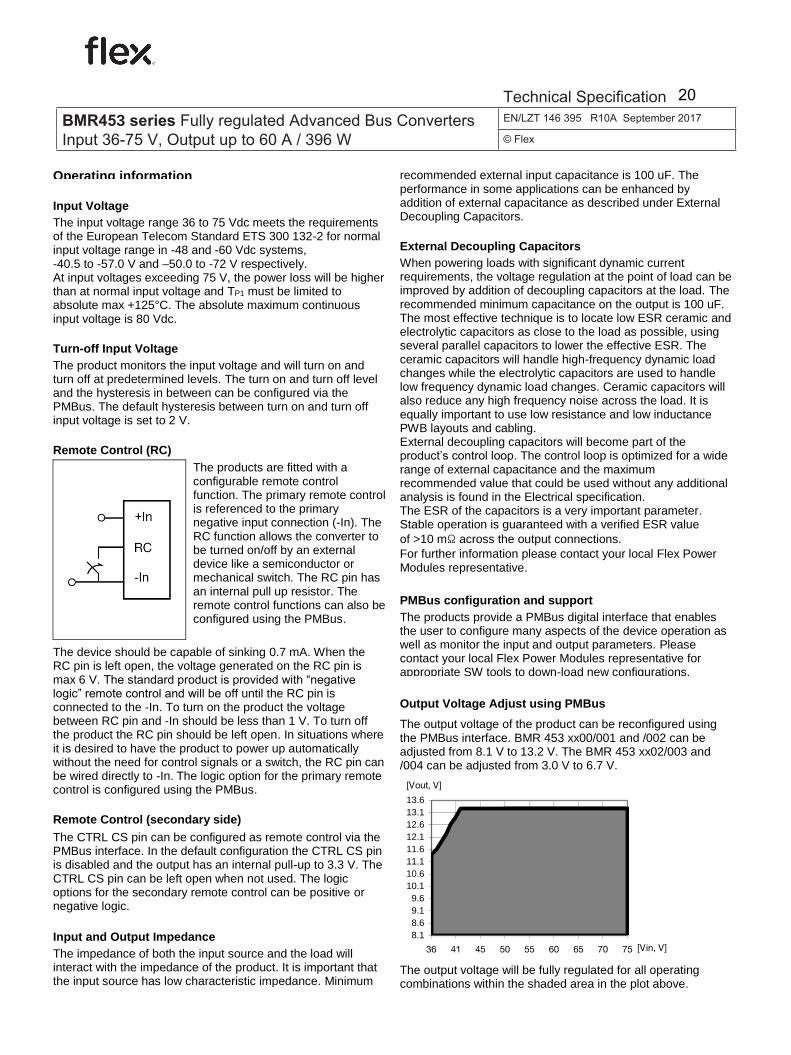
Output Voltage Adjust using PMBus
The output voltage of the product can be reconfigured using the PMBus interface. BMR 453 xx00/001 and /002 can be adjusted from 8.1 V to 13.2 V. The BMR 453 xx02/003 and /004 can be adjusted from 3.0 V to 6.7 V.
8.18.69.19.6
10.110.611.111.612.112.613.113.6
36 41 45 50 55 60 65 70 75 [Vin, V]
[Vout, V]
The output voltage will be fully regulated for all operating combinations within the shaded area in the plot above.
BMR453 series Fully regulated Advanced Bus ConvertersInput 36-75 V, Output up to 60 A / 396 W
SECSUND 30/1301-BMR 453 Uen Approved Checked Date Rev Reference
BNEWIHCLB (Lisa Li) 2017-09-27 N
Operation outside of this area is not recommended for normal use.
Margin Up/Down Controls These controls allow the output voltage to be momentarily adjusted, either up or down, by a nominal 10%. This provides a convenient method for dynamically testing the operation of the load circuit over its supply margin or range. It can also be used to verify the function of supply voltage supervisors. The margin up and down levels of the product can be re-configured using the PMBus interface. Soft-start Power Up
The soft-start control introduces a time-delay (default setting 40 ms) before allowing the output voltage to rise. The default rise time of the ramp up is 10 ms. Power-up is hence completed within 50 ms in default configuration using remote control. When starting by applying input voltage the control circuit boot-up time adds an additional 100 ms delay. The soft-start power up of the product can be reconfigured using the PMBus interface. Remote Sense The products have remote sense that can be used to compensate for voltage drops between the output and the point of load. The sense traces should be located close to the PCB ground layer to reduce noise susceptibility. The remote sense circuitry will compensate for up to 10% voltage drop between +Out pin and the point of load (+Sense). The -Sense pin should be always connected to -Out. When activating remote sense, connect the +Sense pin to the +Input of the load. If the remote sense is not needed +Sense pin should be connected to +Out of the BMR453 unit. To be able to use remote sense the converter must be equipped with a digital connector. Temperature Protection (OTP, UTP) The products are protected from thermal overload by an internal temperature shutdown protection. When TP1 as defined in thermal consideration section is exceeded the product will shut down. The product will make continuous attempts to start up (non-latching mode) and resume normal operation automatically when the temperature has dropped below the temperature threshold, the hysteresis is defined in general electrical specification. The OTP and hysteresis of the product can be re-configured using the PMBus interface. The product has also an under temperature protection. The OTP and UTP fault limit and fault response can be configured via the PMBus. Note: using the fault response “continue without interruption” may cause permanent damage of the product. Over Voltage Protection (OVP) The product has output over voltage protection that will shut down the converter in over voltage conditions (latching mode) The OVP fault level and fault response can be re-configured using the PMBus interface.
Over Current Protection (OCP)
The product includes current limiting circuitry for protection at continuous overload. The module needs RC cycle operation at least once before enters hiccup mode if the maximum output current is exceeded and the output voltage is below 0.3×Vout. The load distribution should be designed for the maximum output short circuit current specified. If for some reason the output should be short circuited, minimum resistance should not be lower than 6 mΩ. The OCP level and fault response can be re-configured using the PMBus interface. The default configuration is set to hiccup mode for the OCP, except for BMR453xxxx/001 (latching OCP). Brick wall OCP mode is also supported in BMR453 series for option. For further information please contact your local Flex Power Modules representative. RC recycle operation as below:
Input Over/Under voltage protection The input of the product can be protected agains high input voltage and low input voltage. The over- and under-voltage fault level and fault response can be configured via the PMBus interface. Pre-bias Start-up
The product has a Pre-bias start up functionality and will not sink current during start up if a pre-bias source is present at the output terminals. Power Good The PG SYNC pin can be configured as an output (POWER GOOD). The power good signal (TTL level) indicates proper operation of the product and can also be used as an error flag indicator. The PG SYNC pin has POWER GOOD as default configuration with the output set as active low. The PG SYNC pin is configured via the PMBus interface. Tracking and External reference The PG SYNC pin can be configured as an input for voltage tracking or an external analogue reference. The PG SYNC pin is configured via the PMBus interface and has default setting Power Good. Send command MFR_MULTI_PIN_CONFIG (0xF9h) with data 0x10h, the module will work in standalone tracking mode; Connect the PG_SYNC pin to the external reference voltage (ground to –OUT), the output voltage will follow this reference voltage with a predefined scale. The max reference voltage is 2.5 V which connects to digital controller's ADC port. The reference voltage / Vout scale factor is stored in MFR_VOUT_ANALOG_SCALE (0xE8h) with default value
Vin
RC_on
RC_off
RC_on
RC_off
BMR453 series Fully regulated Advanced Bus ConvertersInput 36-75 V, Output up to 60 A / 396 W
SECSUND 30/1301-BMR 453 Uen Approved Checked Date Rev Reference
BNEWIHCLB (Lisa Li) 2017-09-27 N
0.175(0xA2CDh), end user can change it by using PMBus command. End user can read the scaled value by command MFR_READ_VOUT_ANALOG_REF (0xE9h). Any changes of using PMBUS command should use command Store Default all (0x11h) to make the change permanent before power off. Switching frequency adjust using PMBus
The switching frequency is set to 140 kHz as default but this can be reconfigured via the PMBus interface. The product is optimized at this frequency but can run at lower and higher frequency, (125 kHz – 150 kHz). However the output performance is not specified if the frequency is changed. Input Transient The BMR453 products have limited ability to react on sudden input voltage changes. As an example the 12 V module BMR453xxxx/001 can have an output voltage deviation of 5 V when a 20 V input step is applied (40 V to 60 V). This is tested with a slew rate of 0.1 V/us on the input voltage change and minimum output capacitance 100 uF. Increasing the output capacitance will improve the result. Parallel Operation with Droop
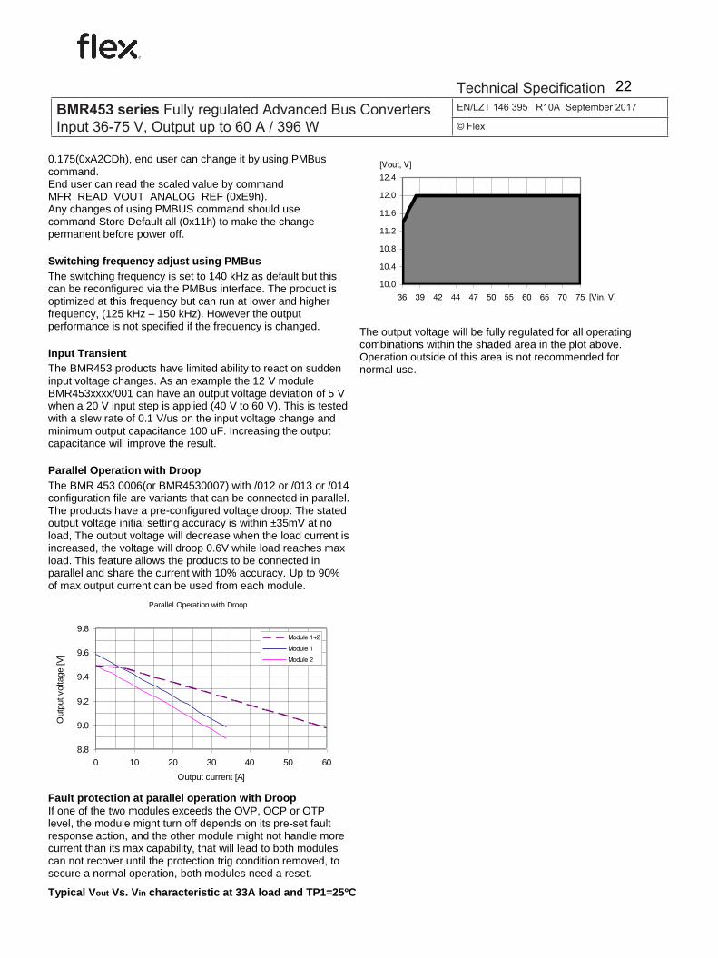
The BMR 453 0006(or BMR4530007) with /012 or /013 or /014 configuration file are variants that can be connected in parallel. The products have a pre-configured voltage droop: The stated output voltage initial setting accuracy is within ±35mV at no load, The output voltage will decrease when the load current is increased, the voltage will droop 0.6V while load reaches max load. This feature allows the products to be connected in parallel and share the current with 10% accuracy. Up to 90% of max output current can be used from each module.
Parallel Operation with Droop
8.8
9.0
9.2
9.4
9.6
9.8
0 10 20 30 40 50 60
Output current [A]
Out
put v
olta
ge [V
]
Module 1+2
Module 1
Module 2
Fault protection at parallel operation with Droop If one of the two modules exceeds the OVP, OCP or OTP level, the module might turn off depends on its pre-set fault response action, and the other module might not handle more current than its max capability, that will lead to both modules can not recover until the protection trig condition removed, to secure a normal operation, both modules need a reset.
Typical Vout Vs. Vin characteristic at 33A load and TP1=25ºC
10.0
10.4
10.8
11.2
11.6
12.0
12.4
36 39 42 44 47 50 55 60 65 70 75 [Vin, V]
[Vout, V]
The output voltage will be fully regulated for all operating combinations within the shaded area in the plot above. Operation outside of this area is not recommended for normal use.
BMR453 series Fully regulated Advanced Bus ConvertersInput 36-75 V, Output up to 60 A / 396 W
SECSUND 30/1301-BMR 453 Uen Approved Checked Date Rev Reference
BNEWIHCLB (Lisa Li) 2017-09-27 N
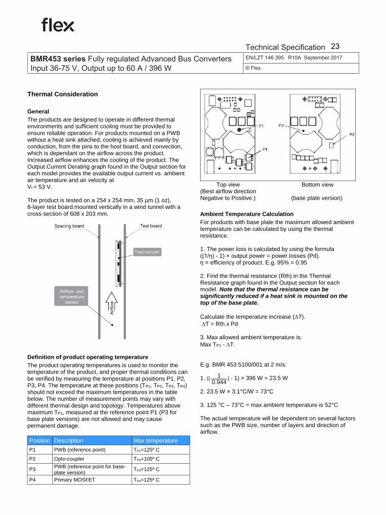
Thermal Consideration General The products are designed to operate in different thermal environments and sufficient cooling must be provided to ensure reliable operation. For products mounted on a PWB without a heat sink attached, cooling is achieved mainly by conduction, from the pins to the host board, and convection, which is dependant on the airflow across the product. Increased airflow enhances the cooling of the product. The Output Current Derating graph found in the Output section for each model provides the available output current vs. ambient air temperature and air velocity at VI = 53 V. The product is tested on a 254 x 254 mm, 35 µm (1 oz), 8-layer test board mounted vertically in a wind tunnel with a cross-section of 608 x 203 mm.
Definition of product operating temperature The product operating temperatures is used to monitor the temperature of the product, and proper thermal conditions can be verified by measuring the temperature at positions P1, P2, P3, P4. The temperature at these positions (TP1, TP2, TP3, TP4) should not exceed the maximum temperatures in the table below. The number of measurement points may vary with different thermal design and topology. Temperatures above maximum TP1, measured at the reference point P1 (P3 for base plate versions) are not allowed and may cause permanent damage. Position Description Max temperature
P1 PWB (reference point) TP1=125º C
P2 Opto-coupler TP2=105º C
P3 PWB (reference point for base-plate version)
TP3=125º C
P4 Primary MOSFET TP4=125º C
Top view Bottom view (Best airflow direction Negative to Positive.) (base plate version)
Ambient Temperature Calculation For products with base plate the maximum allowed ambient temperature can be calculated by using the thermal resistance. 1. The power loss is calculated by using the formula ((1/η) - 1) × output power = power losses (Pd). η = efficiency of product. E.g. 95% = 0.95 2. Find the thermal resistance (Rth) in the Thermal Resistance graph found in the Output section for each model. Note that the thermal resistance can be significantly reduced if a heat sink is mounted on the top of the base plate.
Calculate the temperature increase (T). T = Rth x Pd 3. Max allowed ambient temperature is: Max TP1 - T. E.g. BMR 453 5100/001 at 2 m/s: 1. (( ) - 1) × 396 W = 23.5 W 2. 23.5 W × 3.1°C/W = 73°C 3. 125 °C – 73°C = max ambient temperature is 52°C The actual temperature will be dependent on several factors such as the PWB size, number of layers and direction of airflow.
1 0.944
BMR453 series Fully regulated Advanced Bus ConvertersInput 36-75 V, Output up to 60 A / 396 W
The products provide a PMBus digital interface that enables the user to configure many aspects of the device operation as well as monitor the input and output parameters. The products can be used with any standard two-wire I2C or SMBus host device. In addition, the device is compatible with PMBus version 1.1 and includes an SALERT line to help mitigate bandwidth limitations related to continuous fault monitoring.
Monitoring via PMBus A system controller can monitor a wide variety of different parameters through the PMBus interface. The controller can monitor for fault condition by monitoring the SALERT pin, which will be asserted when any number of pre-configured fault or warning conditions occur. The system controller can also continuously monitor for any number of power conversion parameters including but not limited to the following:
Evaluation software A Configuration Monitoring and Management (CMM) evaluation software, is available for the products. For more information please contact your local Flex Power Modules sales representative.
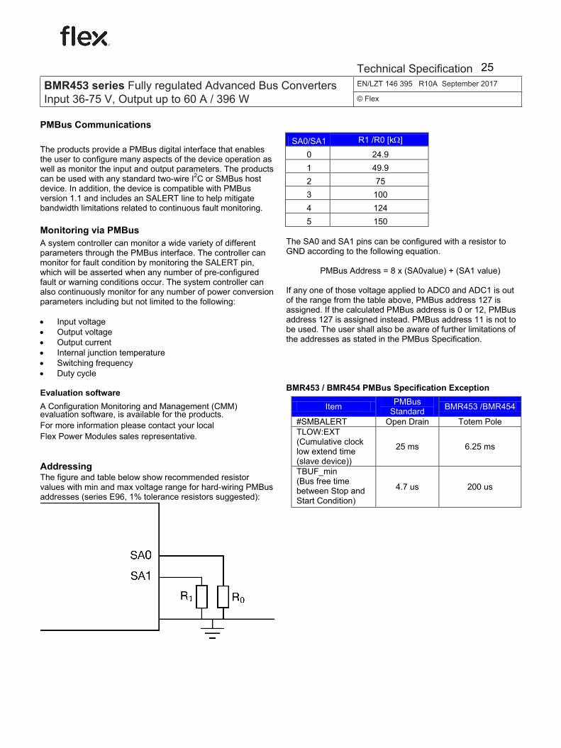
Addressing The figure and table below show recommended resistor values with min and max voltage range for hard-wiring PMBus addresses (series E96, 1% tolerance resistors suggested):
SA0/SA1 R1 /R0 [kΩ]
0 24.9 1 49.9 2 75 3 100 4 124 5 150
The SA0 and SA1 pins can be configured with a resistor to GND according to the following equation.
PMBus Address = 8 x (SA0value) + (SA1 value)
If any one of those voltage applied to ADC0 and ADC1 is out of the range from the table above, PMBus address 127 is assigned. If the calculated PMBus address is 0 or 12, PMBus address 127 is assigned instead. PMBus address 11 is not to be used. The user shall also be aware of further limitations of the addresses as stated in the PMBus Specification.
BMR453 / BMR454 PMBus Specification Exception
Item PMBus Standard BMR453 /BMR454
#SMBALERT Open Drain Totem Pole TLOW:EXT (Cumulative clock low extend time (slave device))
25 ms 6.25 ms
TBUF_min (Bus free time between Stop and Start Condition)
4.7 us 200 us
BMR453 series Fully regulated Advanced Bus ConvertersInput 36-75 V, Output up to 60 A / 396 W
PMBus Commands The DC/DC converter is PMBUS compliant. The following table lists the implemented PMBus commands. For more detailed information see PMBus Power System Management Protocol Specification; Part I – General Requirements, Transport and Electrical Interface and PMBus Power System Management Protocol; Part II – Command Language.
Designation Cmd Impl MFR_DEBUG_BUFF F0h Yes MFR_SETUP_PASSWORD F1h Yes MFR_DISABLE_SECURITY F2h Yes MFR_DEAD_BAND_IOUT_THRESHOLD F3h Yes note1 MFR_SECURITY_BIT_MASK F4h Yes MFR_PRIMARY_TURN F5h Yes note1 MFR_SECONDARY_TURN F6h Yes note1 MFR_SET_DPWM_POLARITY F7h Yes note1 MFR_ILIM_SOFTSTART F8h Yes MFR_MULTI_PIN_CONFIG F9h Yes MFR_DEAD_BAND_VIN_THRESHOLD FAh Yes note1 MFR_DEAD_BAND_VIN_IOUT_HYS FBh Yes note1 MFR_FIRMEWARE_VERSION FCh Yes note1 MFR_MESSAGE_CODE_DEVICE_ID FDh Yes note1 Notes: Cmd is short for Command. Impl is short for Implemented. Note1: the content is protected for being overwritten to secure normal operation Note 2: Power must be kept on at least 700ms after sending STORE_DEFAULT_ALL command for data flash refresh.
BMR453 series Fully regulated Advanced Bus ConvertersInput 36-75 V, Output up to 60 A / 396 W
EPEIHLI 4/1301- BMR453 Uen Approved Checked Date Rev Reference
SEC/D [Julia You] See §1 2013-12-04 K
Mechanical Information - Hole Mount, Open Frame Version
All component placements – whether shown as physical components or symbolical outline – are for reference only and are subject to change throughout the product’s life cycle, unless explicitly described and dimensioned in this drawing.
BMR453 series Fully regulated Advanced Bus ConvertersInput 36-75 V, Output up to 60 A / 396 W
EPEIHLI 4/1301- BMR453 Uen Approved Checked Date Rev Reference
SEC/D [Julia You] See §1 2013-12-04 K
Mechanical Information- Hole Mount, Base Plate Version
All component placements – whether shown as physical components or symbolical outline – are for reference only and are subject to change throughout the product’s life cycle, unless explicitly described and dimensioned in this drawing.
BMR453 series Fully regulated Advanced Bus ConvertersInput 36-75 V, Output up to 60 A / 396 W
EPEIHLI 4/1301- BMR453 Uen Approved Checked Date Rev Reference
SEC/D [Julia You] See §1 2013-12-04 K
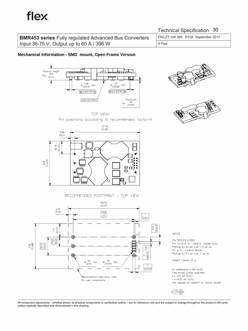
Mechanical Information - SMD mount, Open Frame Version
All component placements – whether shown as physical components or symbolical outline – are for reference only and are subject to change throughout the product’s life cycle, unless explicitly described and dimensioned in this drawing.
BMR453 series Fully regulated Advanced Bus ConvertersInput 36-75 V, Output up to 60 A / 396 W
EPEIHLI 4/1301- BMR453 Uen Approved Checked Date Rev Reference
SEC/D [Julia You] See §1 2013-12-04 K
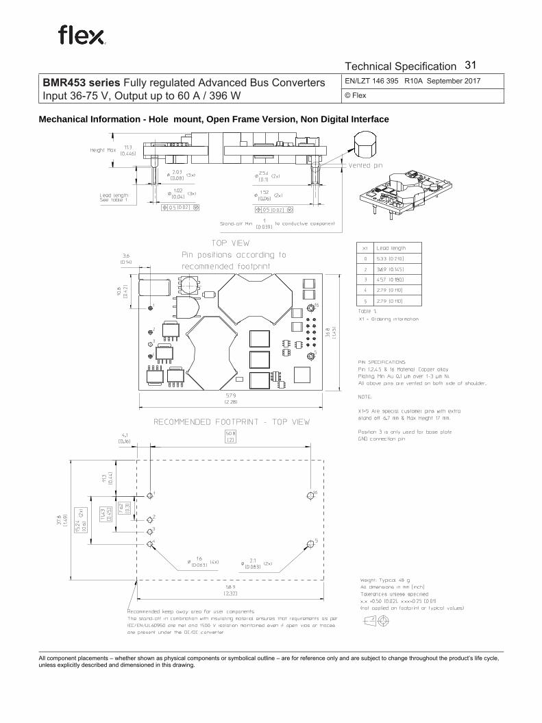
Mechanical Information - Hole mount, Open Frame Version, Non Digital Interface
All component placements – whether shown as physical components or symbolical outline – are for reference only and are subject to change throughout the product’s life cycle, unless explicitly described and dimensioned in this drawing.
BMR453 series Fully regulated Advanced Bus ConvertersInput 36-75 V, Output up to 60 A / 396 W
EPEIHLI 5/1301 BMR 453 Uen Approved Checked Date Rev Reference
SEC/D (Julia You) See §1 2013-11-28 E
Soldering Information – Surface Mounting The surface mount product is intended for forced convection or vapor phase reflow soldering in SnPb and Pb-free processes. The reflow profile should be optimised to avoid excessive heating of the product. It is recommended to have a sufficiently extended preheat time to ensure an even temperature across the host PCB and it is also recommended to minimize the time in reflow. A no-clean flux is recommended to avoid entrapment of cleaning fluids in cavities inside the product or between the product and the host board, since cleaning residues may affect long time reliability and isolation voltage.
Minimum Pin Temperature Recommendations
Pin number 5 is chosen as reference location for the minimum pin temperature recommendation since this will likely be the coolest solder joint during the reflow process.
SnPb solder processes
For SnPb solder processes, a pin temperature (TPIN) in excess of the solder melting temperature, (TL, 183°C for Sn63Pb37) for more than 30 seconds and a peak temperature of 210°C is recommended to ensure a reliable solder joint. For dry packed products only: depending on the type of solder paste and flux system used on the host board, up to a recommended maximum temperature of 245°C could be used, if the products are kept in a controlled environment (dry pack handling and storage) prior to assembly.
General reflow process specifications SnPb eutectic Pb-free
Average ramp-up (TPRODUCT) 3°C/s max 3°C/s max
Typical solder melting (liquidus) temperature
TL 183°C 221°C
Minimum reflow time above TL
30 s 30 s
Minimum pin temperature TPIN 210°C 235°C
Peak product temperature TPRODUC
T 225°C 260°C
Average ramp-down (TPRODUCT)
6°C/s max 6°C/s max
Maximum time 25°C to peak 6 minutes 8 minutes
TPRODUCT maximum TPIN minimum
Time
Pin profile
Product profile
TL
Time in reflow
Time in preheat / soak zone
Time 25°C to peak
Temperature
Lead-free (Pb-free) solder processes
For Pb-free solder processes, a pin temperature (TPIN) in excess of the solder melting temperature (TL, 217 to 221°C for SnAgCu solder alloys) for more than 30 seconds and a peak temperature of 235°C on all solder joints is recommended to ensure a reliable solder joint.
Maximum Product Temperature Requirements
Top of the product PCB near pin 2 is chosen as reference location for the maximum (peak) allowed product temperature (TPRODUCT) since this will likely be the warmest part of the product during the reflow process.
SnPb solder processes
For SnPb solder processes, the product is qualified for MSL 1 according to IPC/JEDEC standard J-STD-020C. During reflow TPRODUCT must not exceed 225 °C at any time.
Pb-free solder processes
For Pb-free solder processes, the product is qualified for MSL 3 according to IPC/JEDEC standard J-STD-020C. During reflow TPRODUCT must not exceed 260 °C at any time.
Dry Pack Information
Products intended for Pb-free reflow soldering processes are delivered in standard moisture barrier bags according to IPC/JEDEC standard J-STD-033 (Handling, packing, shipping and use of moisture/reflow sensitivity surface mount devices). Using products in high temperature Pb-free soldering processes requires dry pack storage and handling. In case the products have been stored in an uncontrolled environment and no longer can be considered dry, the modules must be baked according to J-STD-033. Thermocoupler Attachment
Pin 5 for measurement of minimum Pin (solder joint) temperature TPIN
Pin 2 for measurement of maximum product temperature TPRODUCT
BMR453 series Fully regulated Advanced Bus ConvertersInput 36-75 V, Output up to 60 A / 396 W
EPEIHLI 5/1301 BMR 453 Uen Approved Checked Date Rev Reference
SEC/D (Julia You) See §1 2013-11-28 E
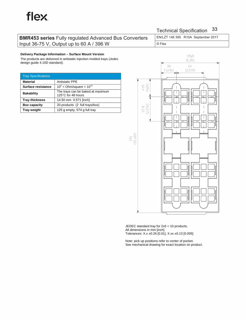
Delivery Package Information – Surface Mount Version
The products are delivered in antistatic injection molded trays (Jedec design guide 4.10D standard).
Tray Specifications
Material Antistatic PPE
Surface resistance 105 < Ohm/square < 1012
Bakability The trays can be baked at maximum 125°C for 48 hours
Tray thickness 14.50 mm 0.571 [inch]
Box capacity 20 products (2 full trays/box)
Tray weight 125 g empty, 574 g full tray
JEDEC standard tray for 2x5 = 10 products. All dimensions in mm [inch] Tolerances: X.x ±0.26 [0.01], X.xx ±0.13 [0.005] Note: pick up positions refer to center of pocket. See mechanical drawing for exact location on product.
BMR453 series Fully regulated Advanced Bus ConvertersInput 36-75 V, Output up to 60 A / 396 W
EPEIHLI 5/1301 BMR 453 Uen Approved Checked Date Rev Reference
SEC/D (Julia You) See §1 2013-11-28 E
Soldering Information – Hole Mounting
The hole mounted product is intended for plated through hole mounting by wave or manual soldering. The pin temperature is specified to maximum to 270°C for maximum 10 seconds. A maximum preheat rate of 4°C/s and maximum preheat temperature of 150°C is suggested. When soldering by hand, care should be taken to avoid direct contact between the hot soldering iron tip and the pins for more than a few seconds in order to prevent overheating. A no-clean flux is recommended to avoid entrapment of cleaning fluids in cavities inside the product or between the product and the host board. The cleaning residues may affect long time reliability and isolation voltage.
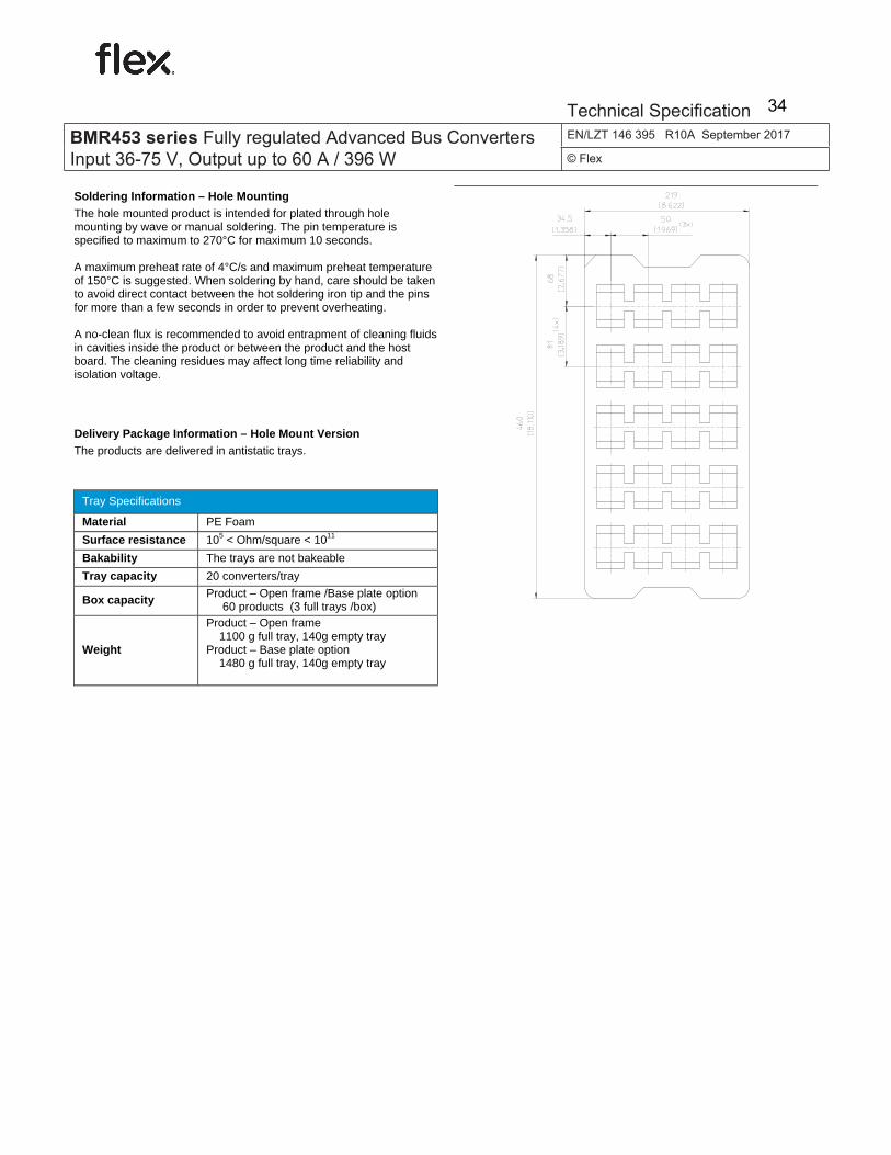
Delivery Package Information – Hole Mount Version
The products are delivered in antistatic trays.
Tray Specifications
Material PE Foam
Surface resistance 105 < Ohm/square < 1011
Bakability The trays are not bakeable
Tray capacity 20 converters/tray
Box capacity Product – Open frame /Base plate option 60 products (3 full trays /box)
Weight
Product – Open frame 1100 g full tray, 140g empty tray Product – Base plate option 1480 g full tray, 140g empty tray
BMR453 series Fully regulated Advanced Bus ConvertersInput 36-75 V, Output up to 60 A / 396 W
Vibration, broad band random IEC 60068-2-64 Fh, method 1 Frequency Spectral density Duration
10 to 500 Hz 0.07 g2/Hz 10 min in each direction
Notes 1 Only for products intended for reflow soldering (surface mount products) 2 Only for products intended for wave soldering (plated through hole products)
BMR453 series Fully regulated Advanced Bus ConvertersInput 36-75 V, Output up to 60 A / 396 W


![TopFX LTD DISCLOSURE AND MARKET DISCIPLINE REPORT 2019 · 7kh suhvhqw uhsruw lv suhsduhg e\ 723); /7' wkh ³&rpsdq\´ d &\suxv ,qyhvwphqw )lup ³&,)´ dxwkrul]hg dqg uhjxodwhg e\](https://static.documents.pub/doc/80x56/5f939c6291986f2b0015ccb9/topfx-ltd-disclosure-and-market-discipline-report-2019-7kh-suhvhqw-uhsruw-lv-suhsduhg.jpg)


