Ultimate Limits of Conventional Ultimate Limits of Conventional Barriers and Barriers and Liners Liners - - Implications for the Implications for the Extendibility of Copper Extendibility of Copper Metallization Metallization Eric Eisenbraun, Tonmoy Chakraborty, and Daniel Greenslit The University at Albany-SUNY College of Nanoscale Science & Engineering
Transcript
Ultimate Limits of Conventional Ultimate Limits of Conventional Barriers and Barriers and
LinersLiners--Implications for the Implications for the Extendibility of Copper Extendibility of Copper
MetallizationMetallizationEric Eisenbraun,
Tonmoy Chakraborty, and Daniel GreenslitThe University at Albany-SUNY
College of Nanoscale Science & Engineering
OutlineOutline
• Introduction: ALD-based liners for Cu metallization– Rationale for directly platable liners
• Development of directly platable liners– Material and process concepts– Optimization of liner chemistry– Microstructural properties– Simultaneous liner and barrier functionality – Integration properties– Extendibility-novel materials
• Summary and conclusions
2
Problem Statement: Problem Statement: Scalability of Barrier/SeedScalability of Barrier/Seed
§ PVD barriers look to be functional down to 22nm§ Scalability past this is not clear
due to lack of continuity on the sidewalls
§ ALD, self-formed barriers being studied
§ PVD Cu seed conformality and continuity is more problematic in the short term§ Seed repair§ ALD seed
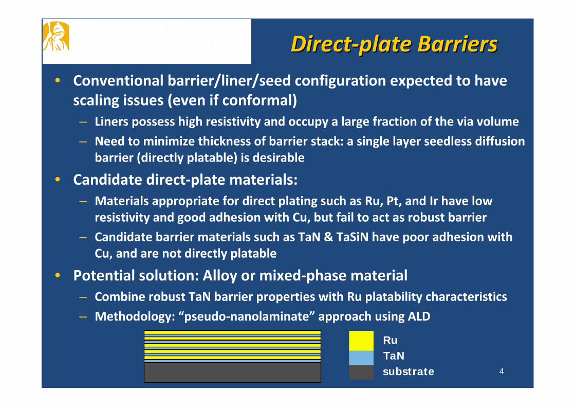
DirectDirect--plate Barriersplate Barriers• Conventional barrier/liner/seed configuration expected to have
scaling issues (even if conformal)– Liners possess high resistivity and occupy a large fraction of the via volume– Need to minimize thickness of barrier stack: a single layer seedless diffusion
barrier (directly platable) is desirable
• Candidate direct-plate materials:– Materials appropriate for direct plating such as Ru, Pt, and Ir have low
resistivity and good adhesion with Cu, but fail to act as robust barrier– Candidate barrier materials such as TaN & TaSiN have poor adhesion with
Cu, and are not directly platable
• Potential solution: Alloy or mixed-phase material– Combine robust TaN barrier properties with Ru platability characteristics– Methodology: “pseudo-nanolaminate” approach using ALD
4substrateTaNRu
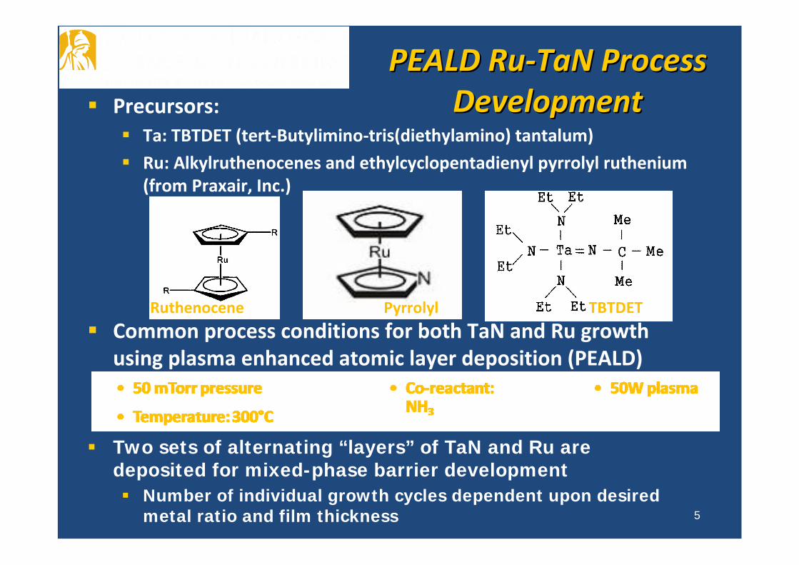
PEALD RuPEALD Ru--TaN Process TaN Process DevelopmentDevelopment§ Precursors:
§ Common process conditions for both TaN and Ru growth using plasma enhanced atomic layer deposition (PEALD)
§ Two sets of alternating “layers” of TaN and Ru are deposited for mixed-phase barrier development§ Number of individual growth cycles dependent upon desired
metal ratio and film thickness 5
Ruthenocene TBTDETPyrrolyl
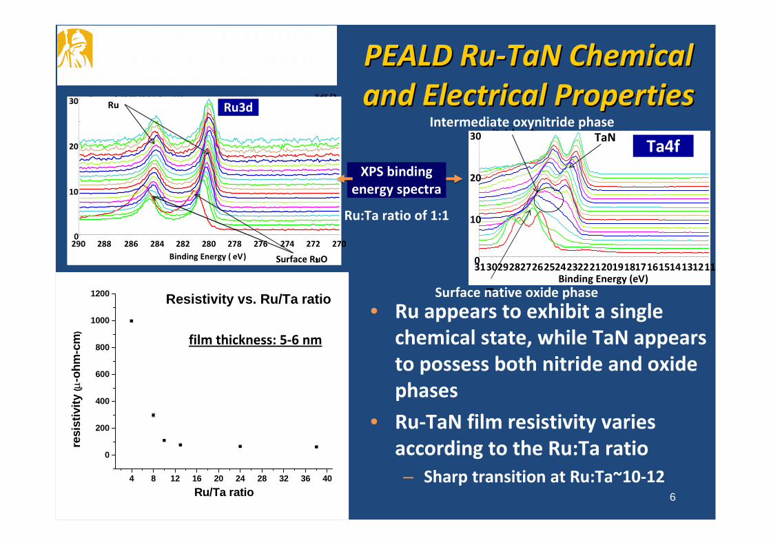
PEALD RuPEALD Ru--TaN Chemical TaN Chemical and Electrical Propertiesand Electrical Properties
4 8 12 16 20 24 28 32 36 40
0
200
400
600
800
1000
1200 Resistivity vs. Ru/Ta ratio
resi
stiv
ity
(m-o
hm
-cm
)
Ru/Ta ratio 6
• Ru appears to exhibit a single chemical state, while TaN appears to possess both nitride and oxide phases
• Ru-TaN film resistivity varies according to the Ru:Ta ratio– Sharp transition at Ru:Ta~10-12
0
10
20
30
111213141516171819202122232425262728293031Binding Energy (eV)
–
nitride phase TaN–22.5 eV
0
10
20
30
111213141516171819202122232425262728293031Binding Energy (eV)
–
Intermediate oxynitride phaseTaN Ta4f
0
10
20
30
270272274276278280282284286288290Binding Energy ( eV) RuO 2 –
– 3d5/2 (280.1 eV )
Ru – 3d3/2 (284.2 eV )
RuO 2 – 3d3/2
0
10
20
30
270272274276278280282284286288290Binding Energy ( eV) Surface RuO2
Ru Ru3d
XPS binding energy spectra
film thickness: 5-6 nm
Ru:Ta ratio of 1:1
Surface native oxide phase
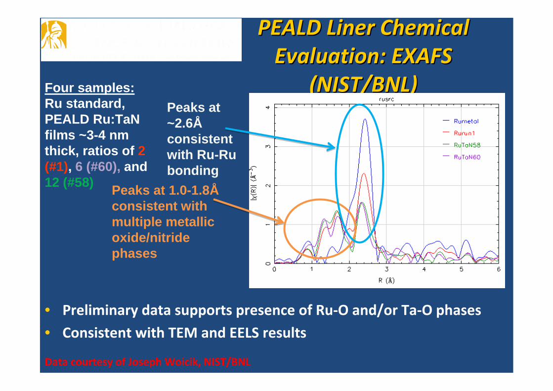
PEALD Liner Chemical PEALD Liner Chemical Evaluation: EXAFS Evaluation: EXAFS
(NIST/BNL)(NIST/BNL)
• Preliminary data supports presence of Ru-O and/or Ta-O phases• Consistent with TEM and EELS results
Data courtesy of Joseph Woicik, NIST/BNL
Peaks at 1.0-1.8Åconsistent with multiple metallic oxide/nitride phases
Peaks at ~2.6Åconsistent with Ru-Ru bonding
Four samples: Ru standard, PEALD Ru:TaN films ~3-4 nm thick, ratios of 2 (#1), 6 (#60), and 12 (#58)
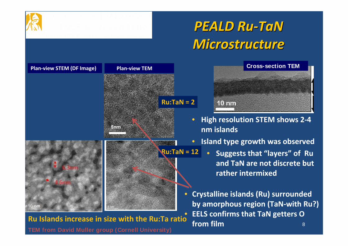
PEALD RuPEALD Ru--TaN TaN MicrostructureMicrostructure
8
• High resolution STEM shows 2-4 nm islands
• Island type growth was observed • Suggests that “layers” of Ru
and TaN are not discrete but rather intermixed
TEM from David Muller group (Cornell University)
Plan-view TEM Plan-view STEM (DF Image)
• Crystalline islands (Ru) surrounded by amorphous region (TaN-with Ru?)
• EELS confirms that TaN getters O from film
Ru:TaN = 2
Ru:TaN = 12
Ru Islands increase in size with the Ru:Ta ratio
Cross-section TEM
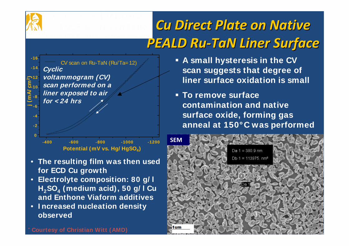
Cu Direct Plate on Native Cu Direct Plate on Native PEALD RuPEALD Ru--TaN Liner SurfaceTaN Liner Surface
9
-400 -600 -800 -1000 -1200
0
-2
-4
-6
-8
-10
-12
-14
-16
j (m
A/c
m2)
Potential (mV vs. Hg/HgSO4)
CV scan on Ru-TaN (Ru/Ta=12)Cyclic voltammogram (CV) scan performed on a liner exposed to air for <24 hrs
§ A small hysteresis in the CV scan suggests that degree of liner surface oxidation is small
§ To remove surface contamination and native surface oxide, forming gas anneal at 150°C was performed
• The resulting film was then used for ECD Cu growth
• Electrolyte composition: 80 g/l H2SO4 (medium acid), 50 g/l Cu and Enthone Viaform additives
• Increased nucleation density observed
* Courtesy of Christian Witt (AMD)
SEM
12 16 20 24 28 32
84
86
88
90
60
90
120
150
180
Barrier resistivity (µ
-oh
m-cm
)% (
111)
Inte
nsi
ty-p
late
d C
u
Ru:Ta ratio in Ru-TaN film
1 2 3 4 5
72
76
80
84
88
400
800
1200
1600
2000
%(1
11)
Inte
nsi
ty-p
late
d C
uRu-TaN film thickness (nm)
Barrier resistivity (µ
-oh
m-cm
)
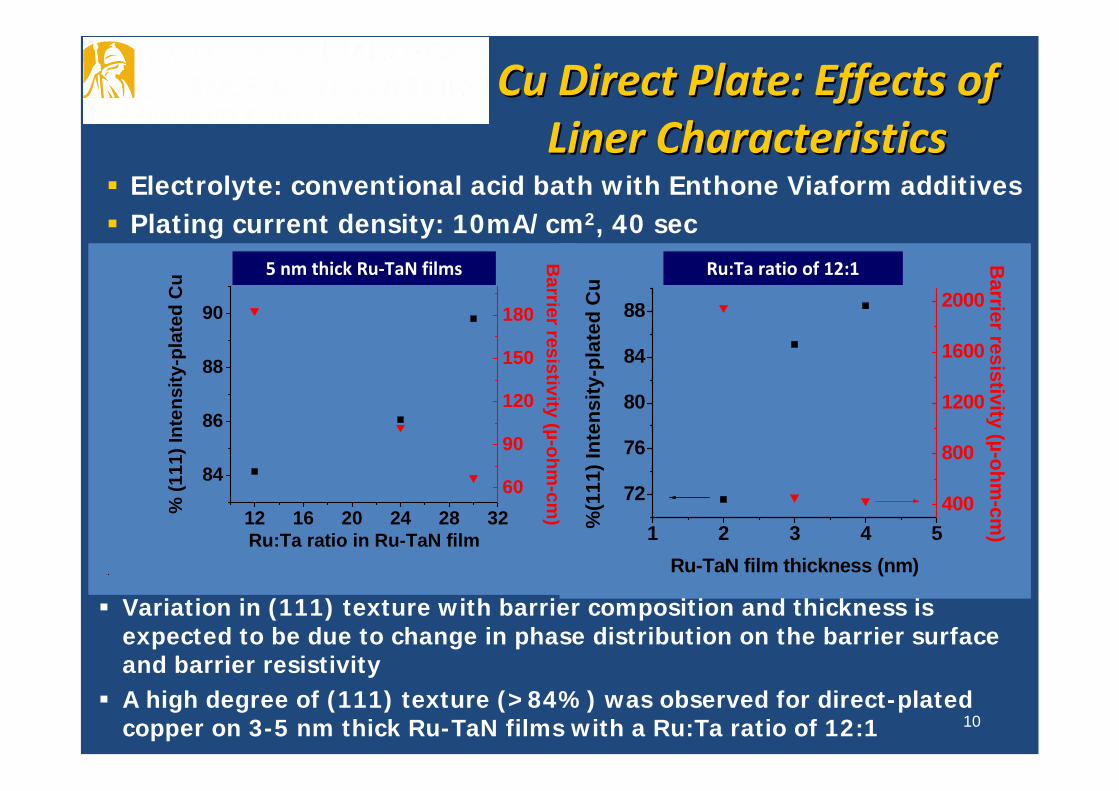
Cu Direct Plate: Effects of Cu Direct Plate: Effects of Liner CharacteristicsLiner Characteristics
§ Electrolyte: conventional acid bath with Enthone Viaform additives§ Plating current density: 10mA/cm2, 40 sec
10
§ Variation in (111) texture with barrier composition and thickness is expected to be due to change in phase distribution on the barrier surface and barrier resistivity
§ A high degree of (111) texture (>84%) was observed for direct-plated copper on 3-5 nm thick Ru-TaN films with a Ru:Ta ratio of 12:1
Ru:Ta ratio of 12:15 nm thick Ru-TaN films
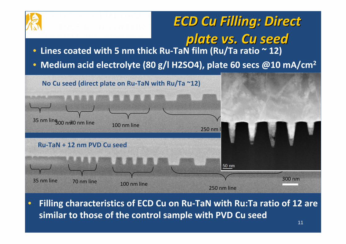
ECD Cu Filling: Direct ECD Cu Filling: Direct plate vs. Cu seedplate vs. Cu seed
11
• Filling characteristics of ECD Cu on Ru-TaN with Ru:Ta ratio of 12 are similar to those of the control sample with PVD Cu seed
No Cu seed (direct plate on Ru-TaN with Ru/Ta ~12)
300 nm70 nm line 100 nm line250 nm line
35 nm line
Ru-TaN + 12 nm PVD Cu seed
300 nm70 nm line 100 nm line250 nm line
35 nm line
• Lines coated with 5 nm thick Ru-TaN film (Ru/Ta ratio ~ 12)• Medium acid electrolyte (80 g/l H2SO4), plate 60 secs @10 mA/cm2
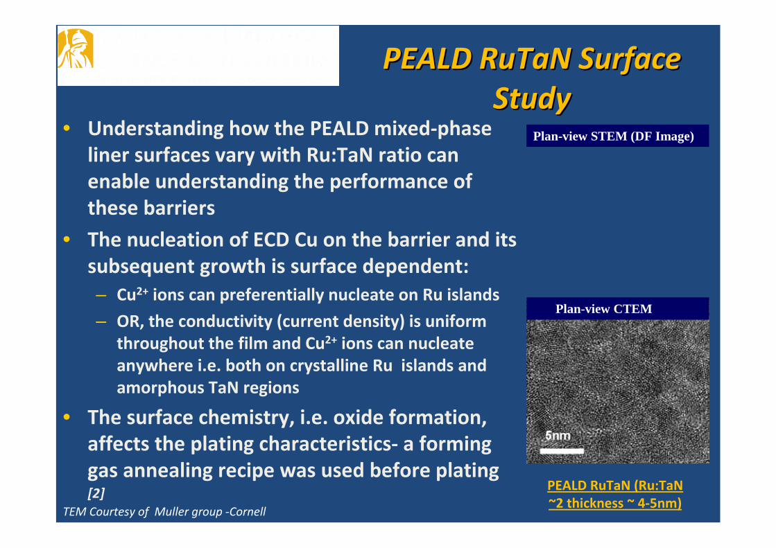
• Understanding how the PEALD mixed-phase liner surfaces vary with Ru:TaN ratio can enable understanding the performance of these barriers
• The nucleation of ECD Cu on the barrier and its subsequent growth is surface dependent:– Cu2+ ions can preferentially nucleate on Ru islands– OR, the conductivity (current density) is uniform
throughout the film and Cu2+ ions can nucleate anywhere i.e. both on crystalline Ru islands and amorphous TaN regions
• The surface chemistry, i.e. oxide formation, affects the plating characteristics- a forming gas annealing recipe was used before plating [2]
Plan-view CTEM
Plan-view STEM (DF Image)
PEALD RuTaN (Ru:TaN ~2 thickness ~ 4-5nm)
TEM Courtesy of Muller group -Cornell
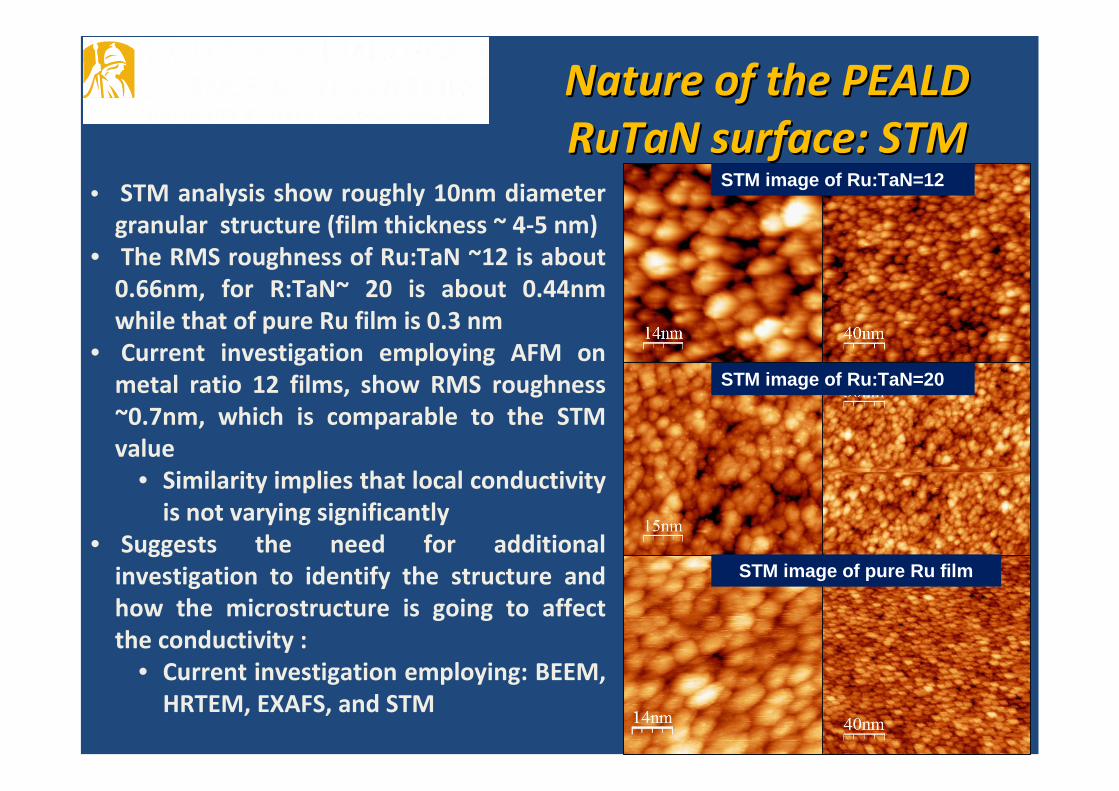
Nature of the PEALD Nature of the PEALD RuTaN surface: STMRuTaN surface: STM
• The RMS roughness of Ru:TaN ~12 is about 0.66nm, for R:TaN~ 20 is about 0.44nm while that of pure Ru film is 0.3 nm
• Current investigation employing AFM on metal ratio 12 films, show RMS roughness ~0.7nm, which is comparable to the STM value
• Similarity implies that local conductivity is not varying significantly
• Suggests the need for additional investigation to identify the structure and how the microstructure is going to affect the conductivity :
• Current investigation employing: BEEM, HRTEM, EXAFS, and STM
STM image of Ru:TaN=12
STM image of Ru:TaN=20
STM image of pure Ru film
HRTEM of Ru:TaN=12
HRTEM of pure TaN
HRTEM of pure Ru
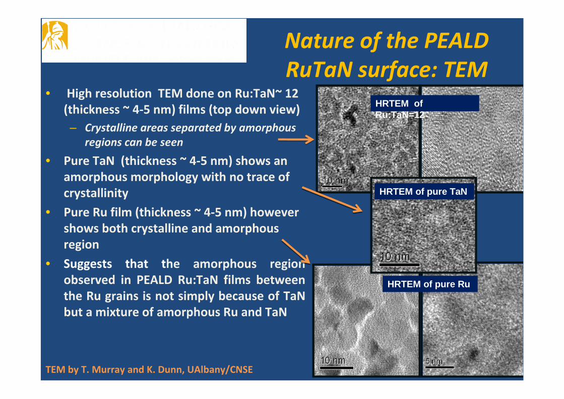
Nature of the PEALD RuTaN surface: TEM
• High resolution TEM done on Ru:TaN~ 12 (thickness ~ 4-5 nm) films (top down view) – Crystalline areas separated by amorphous
regions can be seen
• Pure TaN (thickness ~ 4-5 nm) shows an amorphous morphology with no trace of crystallinity
• Pure Ru film (thickness ~ 4-5 nm) however shows both crystalline and amorphous region
• Suggests that the amorphous region observed in PEALD Ru:TaN films between the Ru grains is not simply because of TaN but a mixture of amorphous Ru and TaN
TEM by T. Murray and K. Dunn, UAlbany/CNSE
140 160 180 200 220 240 2600.0
2.0x10¹³
4.0x10¹³
6.0x10¹³
8.0x10¹³
Ru/Ta=12 Ru/Ta=24 Ru/Ta=30 TaN
ion
s/cm
2
Stress temperature (deg C)
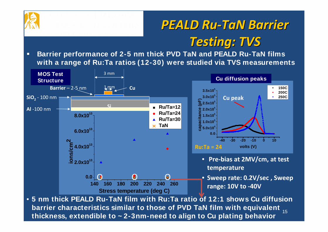
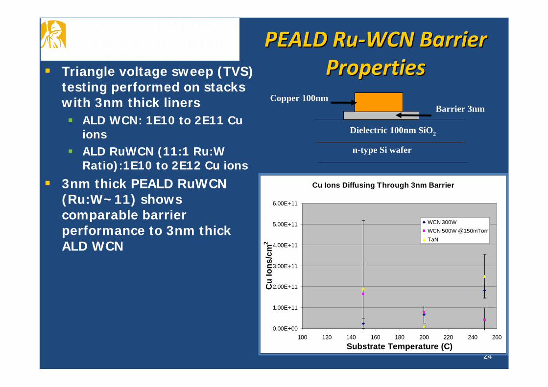
PEALD RuPEALD Ru--TaN Barrier TaN Barrier Testing: TVSTesting: TVS
15
§ Barrier performance of 2-5 nm thick PVD TaN and PEALD Ru-TaN films with a range of Ru:Ta ratios (12-30) were studied via TVS measurements
Cu
SiO2 - 100 nm
MOS Test Structure
3 mm
1 mmBarrier – 2-5 nm
SiAl -100 nm
• Pre-bias at 2MV/cm, at test temperature
• Sweep rate: 0.2V/sec , Sweep range: 10V to -40V
-40 -30 -20 -10 0 10
0.0
5.0x10⁴
1.0x10⁵
1.5x10⁵
2.0x10⁵
2.5x10⁵
3.0x10⁵
3.5x10⁵ 150C 200C 250C
cap
acit
ance
(p
F)
volts (V)
• 5 nm thick PEALD Ru-TaN film with Ru:Ta ratio of 12:1 shows Cu diffusion barrier characteristics similar to those of PVD TaN film with equivalent thickness, extendible to ~2-3nm-need to align to Cu plating behavior
Ru:Ta = 24
Cu peak
OOO
Cu diffusion peaks
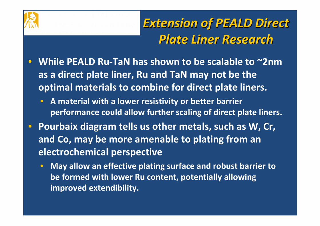
Extension of PEALD Direct Extension of PEALD Direct Plate Liner ResearchPlate Liner Research
• While PEALD Ru-TaN has shown to be scalable to ~2nm as a direct plate liner, Ru and TaN may not be the optimal materials to combine for direct plate liners. • A material with a lower resistivity or better barrier
performance could allow further scaling of direct plate liners.
• Pourbaix diagram tells us other metals, such as W, Cr, and Co, may be more amenable to plating from an electrochemical perspective• May allow an effective plating surface and robust barrier to
be formed with lower Ru content, potentially allowing improved extendibility.
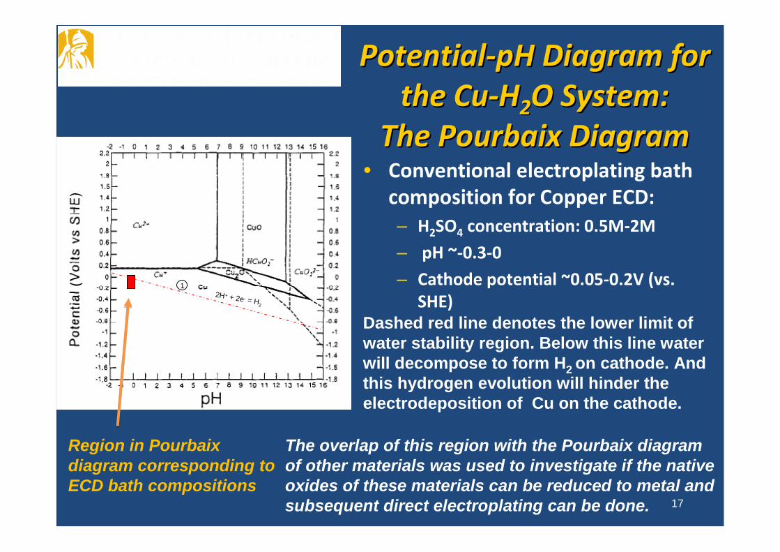
PotentialPotential--pH Diagram for pH Diagram for the Cuthe Cu--HH22O System: O System:
The Pourbaix DiagramThe Pourbaix Diagram• Conventional electroplating bath
Region in Pourbaix diagram corresponding to ECD bath compositions
2H+ + 2e- = H2
1
Dashed red line denotes the lower limit of water stability region. Below this line water will decompose to form H2 on cathode. And this hydrogen evolution will hinder the electrodeposition of Cu on the cathode.
The overlap of this region with the Pourbaix diagram of other materials was used to investigate if the native oxides of these materials can be reduced to metal and subsequent direct electroplating can be done.
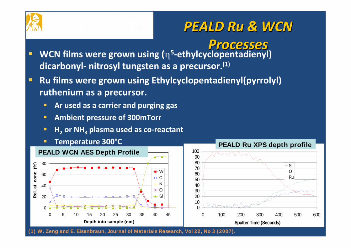
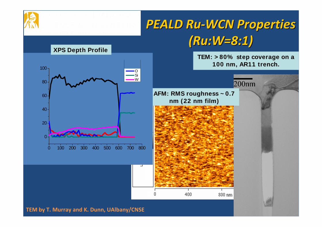
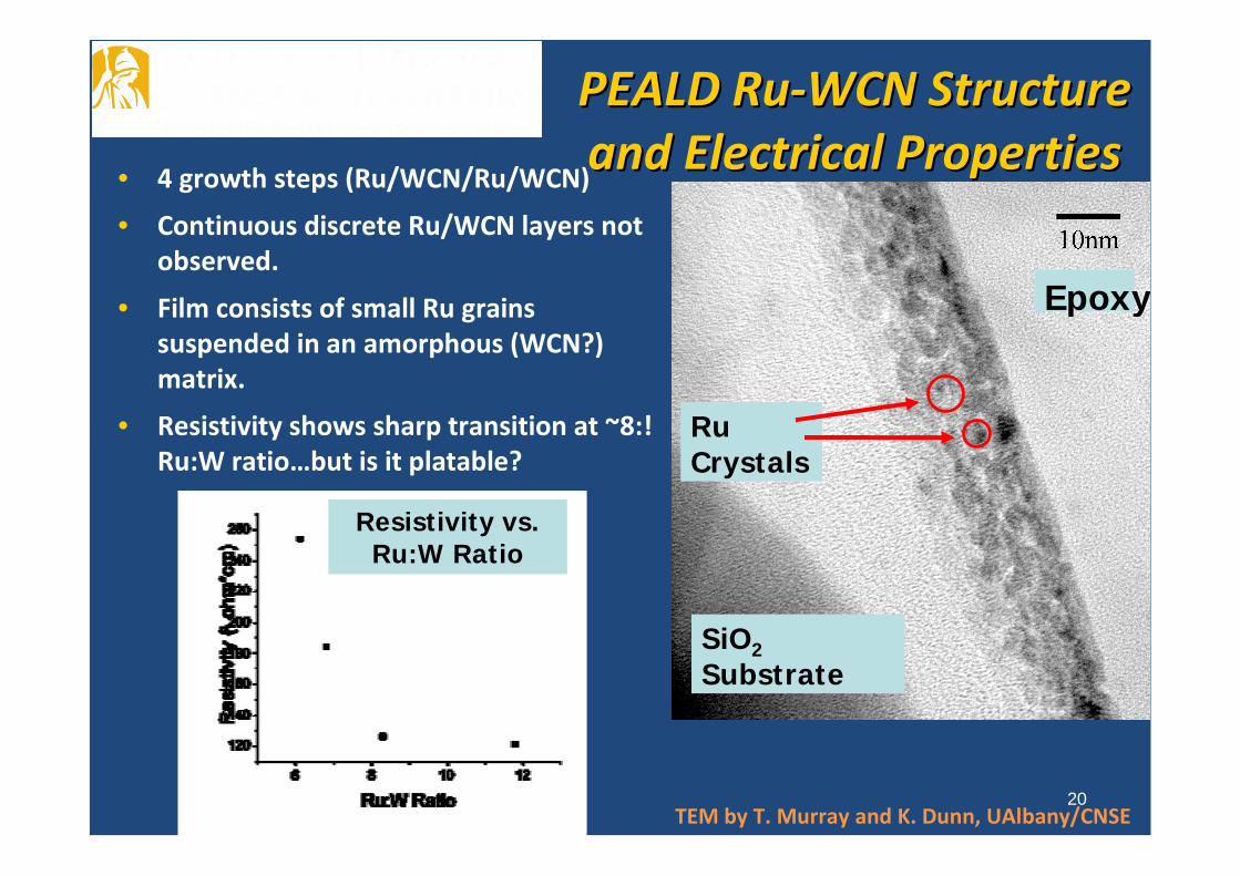
PEALD Ru & WCN PEALD Ru & WCN ProcessesProcesses
200 nm
§ WCN films were grown using (h5-ethylcyclopentadienyl) dicarbonyl- nitrosyl tungsten as a precursor.(1)
§ Ru films were grown using Ethylcyclopentadienyl(pyrrolyl) ruthenium as a precursor.§ Ar used as a carrier and purging gas§ Ambient pressure of 300mTorr§ H2 or NH3 plasma used as co-reactant§ Temperature 300°C
(1) W. Zeng and E. Eisenbraun, Journal of Materials Research, Vol 22, No 3 (2007).
• Film consists of small Ru grains suspended in an amorphous (WCN?) matrix.
• Resistivity shows sharp transition at ~8:! Ru:W ratio…but is it platable?
20
SiO2Substrate
Epoxy
Ru Crystals
TEM by T. Murray and K. Dunn, UAlbany/CNSE
Resistivity vs. Ru:W Ratio
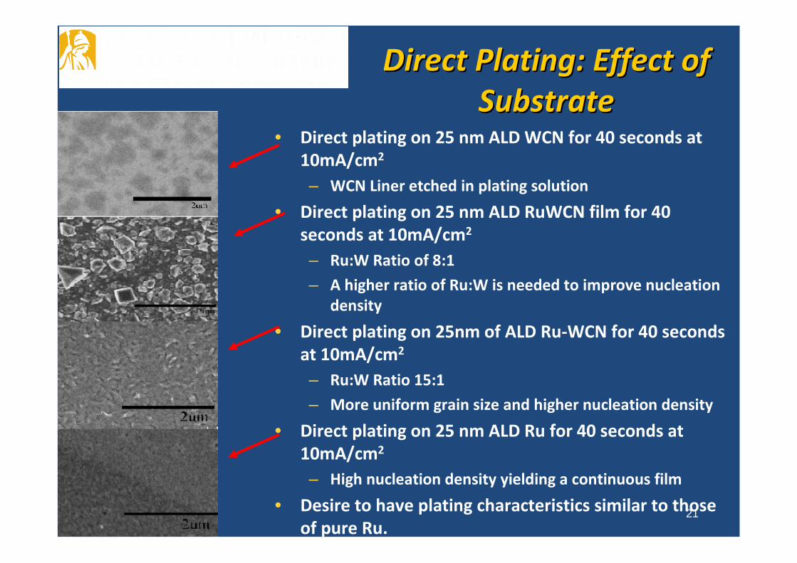
Direct Plating: Effect of Direct Plating: Effect of SubstrateSubstrate
21
• Direct plating on 25 nm ALD WCN for 40 seconds at 10mA/cm2
– WCN Liner etched in plating solution
• Direct plating on 25 nm ALD RuWCN film for 40 seconds at 10mA/cm2
– Ru:W Ratio of 8:1– A higher ratio of Ru:W is needed to improve nucleation
density
• Direct plating on 25nm of ALD Ru-WCN for 40 seconds at 10mA/cm2
– Ru:W Ratio 15:1– More uniform grain size and higher nucleation density
• Direct plating on 25 nm ALD Ru for 40 seconds at 10mA/cm2
– High nucleation density yielding a continuous film
• Desire to have plating characteristics similar to those of pure Ru.
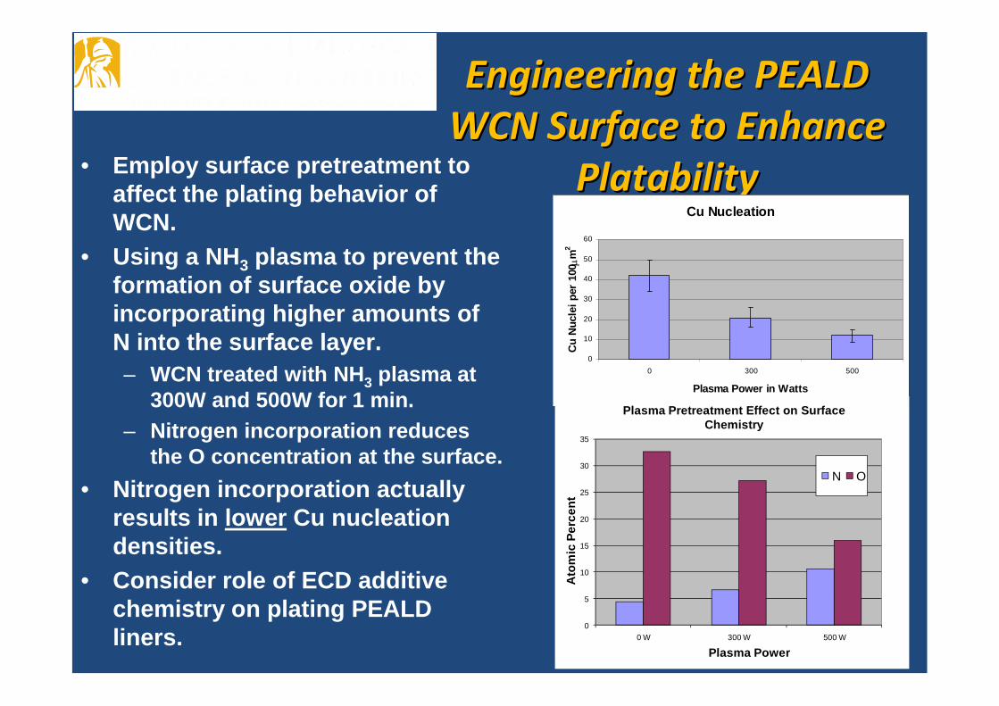
Engineering the PEALD Engineering the PEALD WCN Surface to Enhance WCN Surface to Enhance
PlatabilityPlatability• Employ surface pretreatment to affect the plating behavior of WCN.
• Using a NH3 plasma to prevent the formation of surface oxide by incorporating higher amounts of N into the surface layer.– WCN treated with NH3 plasma at
300W and 500W for 1 min.
– Nitrogen incorporation reduces the O concentration at the surface.
• Nitrogen incorporation actually results in lower Cu nucleation densities.
• Consider role of ECD additive chemistry on plating PEALD liners.
Cu Nucleation
0
10
20
30
40
50
60
0 300 500
Plasma Power in Watts
Cu
Nu
clei
per
100mm
2
0
5
10
15
20
25
30
35
0 W 300 W 500 W
Ato
mic
Per
cen
t
Plasma Power
Plasma Pretreatment Effect on Surface Chemistry
N O
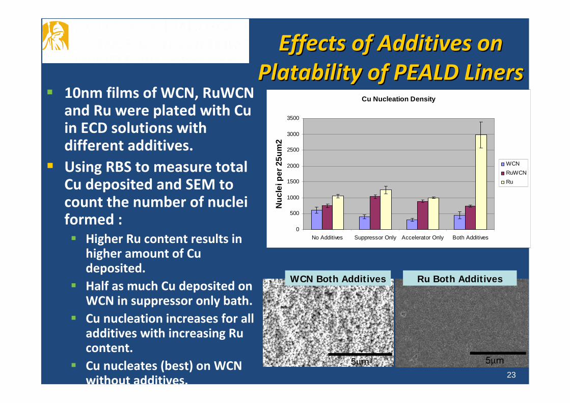
Effects of Additives on Effects of Additives on Platability of PEALD LinersPlatability of PEALD Liners
§ 10nm films of WCN, RuWCN and Ru were plated with Cu in ECD solutions with different additives.
§ Using RBS to measure total Cu deposited and SEM to count the number of nuclei formed :§ Higher Ru content results in
higher amount of Cu deposited.
§ Half as much Cu deposited on WCN in suppressor only bath.
§ Cu nucleation increases for all additives with increasing Ru content.
§ Cu nucleates (best) on WCN without additives. 23
Cu Nucleation Density
0
500
1000
1500
2000
2500
3000
3500
No Additives Suppressor Only Accelerator Only Both Additives
• Samples epoxied to stubs and mechanically strained to measure tensile adhesion.
• Preliminary pull testing results indicate PEALD WCN and RuWCN exhibit the highest tensile strength.
25
Tensile stress applied
Adhesion Testing
0
5
10
15
20
25
Ru TaN WCN RuWCN
Liner Material (3nm)
Ten
sile
Str
ess
in M
Pa
Researching Novel Material Researching Novel Material Options for Extendible Options for Extendible
PEALD Direct Plate LinerPEALD Direct Plate Liner• For direct plate liner work, research to date has focused on PEALD-
grown versions of common liner materials (TaN, WCN, TiN).– These tend to have intrinsic scalability issues due to their higher resistances
caused by the incorporation of N and C into the metals.
• It would potentially be advantageous with respect to platability to have a metal that acted as a diffusion barrier which did not require the use of (much) N or C.– However, one which still enables direct plating as described by the Pourbaix
diagram.
• Co and Cr considered as potentially interesting materials.– Native oxides of Co and Cr electrochemically reduced at -0.4V and -1V,
respectively
Cr Barrier Literature Cr Barrier Literature OverviewOverview• Ezer used 10nm Cr films, annealed Cr/Cu
stacks at 400°C for 30 min.1
– RBS shows that at temperatures up to 400°C there is no signs of inter-diffusion between the Cu and the Cr layers.
• AES sputter depth profiling (Shih) confirms this in a similar experiment.2
• RTA of Cr films in N2 resulted in the incorporation of N into the surface of the Cr film.3
– This then increased the Cr barrier stability to 700°C.
• Potential for nanoengineered Cr films to be a suitable barrier.– The platability of Cr has not been reported in
barrier research studies1) Ezer, Y. et al. Materials Research Bulletin, Vol. 33 (9) 19982) Shih, T et al. J. Appl. Phys., 70 (6) 19913) Chuang, J. et al., Journal of the Electrochemical Society, 146(7) 1999.
ECD Cu on Cr: Initial ECD Cu on Cr: Initial ObservationsObservations
• Evaluate ECD Cu on a ~30nm layer of PVD Cr.– Cr Rs=34 ohm/sq
• Top down SEM imaging shows rounded islands of Cu forming from the ECD process.
• Looking at these structures from the side the islands appear to be non-wetting hemispheres.
• 2nm PVD Cr with 1 nm of PEALD Ru on top yields a uniform Cu layer.– Potential applicability as a direct plate
surface…but is it a good barrier at this thickness?
Cr as a Cu Barrier: Initial Cr as a Cu Barrier: Initial ObservationsObservations
• While literature has shown ~10nm thick PVD Cr to be an effective Cu diffusion barrier up to 400°C, it would be advantageous to compare more relevant ALD-grown samples against known diffusion barriers.
• 3nm PVD Cr was used in TVS testing and shows to perform similar to ALD TaN and WCN.
• PEALD Cr process using Cr(acac)2 evaluated– Cr PEALD process susceptible to
metallic contamination from chamber
29
Cu Ions Diffusing Through 3nm Barrier
1.00E+09
1.00E+10
1.00E+11
1.00E+12
1.00E+13
150 200 250
Substrate Temperature (C)
Cu
Io
ns/
cm2
PVD Cr
WCN
TaN
RuRu--Co PEALD Process Co PEALD Process DevelopmentDevelopment
• Explore cobaltocene as a Co source– Precursor thermodynamic properties similar to Ru source for metal
mixture processing– Plasma H2 as a co-reactant
• Initial results indicate Ru:Co ~5:1 may be useful for direct plate– ~100 Ohms @ ~6nm, good Cu nucleation– TVS: similar to TaN as barrier
0 200 400 600 800 1000
Channel
0
10
20
30
40
50
Nor
malized
Yield
0.5 1.0 1.5
Energy (MeV)
C53654 090110_RuCo6Simulation of Co-Ru/Si-O/Si
SummarySummary
• Research has focused on Cu interconnect extendibility via scalability of novel liner material and process solutions.
• Potentially useful approaches have been developed– PEALD RuTaN appears to be functional to ~2nm– Planning evaluation of integration properties with SRC
partners in the near future.
• Where do we go from here?– Self formed barriers?– Monolayer deposition?
31
AcknowledgementsAcknowledgements
• Tonmoy Chakraborty and Dan Greenslit for doing the work!• Kathleen Dunn and Thomas Murray (CNSE) and David Muller
(Cornell) for TEM support and research collaborations.• Alan West (Columbia) and Cev Noyan (Columbia) for
collaboration on plating and x-ray analyses• This research was supported by the Semiconductor Research
Corporation (SRC) and the New York State Foundation for Science, Technology and Innovation (NYSTAR) under the New York Center for Advanced Interconnect Science and Technology (NY-CAIST).