• Tablet PC and external storage with high speed interfaces
• Applications requiring high ESD performance in small packages
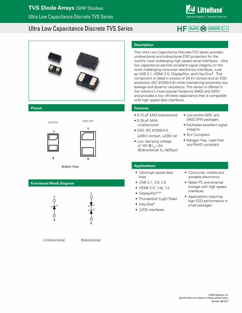
Pinout
Bottom View
1
2
1
2
Functional Block Diagram
1
2
1
2
Unidirectional Bidirectional
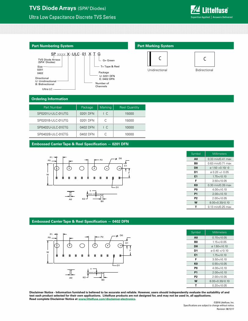
Ultra Low Capacitance Discrete TVS Series
0402 DFN0201DFN
Description
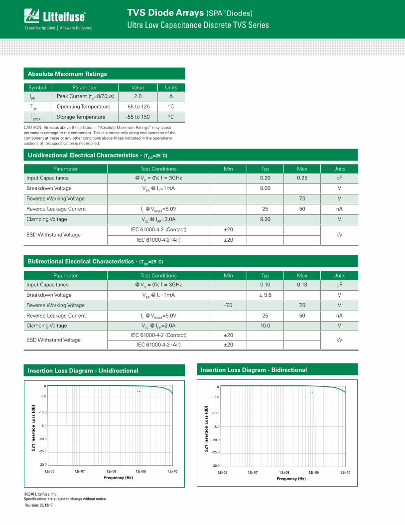
This Ultra Low Capacitance Discrete TVS series provides unidirectional and bidirectional ESD protection for the world’s most challenging high speed serial interfaces. Ultra low capacitance permits excellent signal integrity on the most challenging consumer electronics interfaces, such as USB 3.1, HDMI 2.0, DisplayPort, and V-by-One®. This component is rated in excess of 20 kV contact and air ESD protection (IEC 61000-4-2) while maintaining extremely low leakage and dynamic resistance. This series is offered in the industry’s most popular footprints (0402 and 0201) and provides a low off-state capacitance that is compatible with high speed data interfaces.
Features
ELVRoHS Pb GREEN
• 0.13 pF MAX bidirectional
• 0.25 pF MAX unidirectional
• ESD, IEC 61000-4-2,
±20kV contact, ±20kV air
• Low clamping voltage of 10V @ IPP=2A (Bidirectional) (tP=8/20μs)
CAUTION: Stresses above those listed in “Absolute Maximum Ratings” may cause permanent damage to the component. This is a stress only rating and operation of the component at these or any other conditions above those indicated in the operational sections of this specification is not implied.
Flammability UL Recognized epoxy meeting flammability rating V-0.
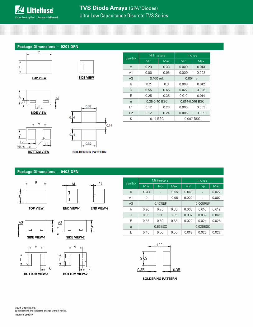
Notes : 1. All dimensions are in millimeters2. Dimensions include solder plating.3. Dimensions are exclusive of mold flash & metal burr.4. Blo is facing up for mold and facing down for trim/form, i.e. reverse trim/form.5. Package surface matte finish VDI 11-13.
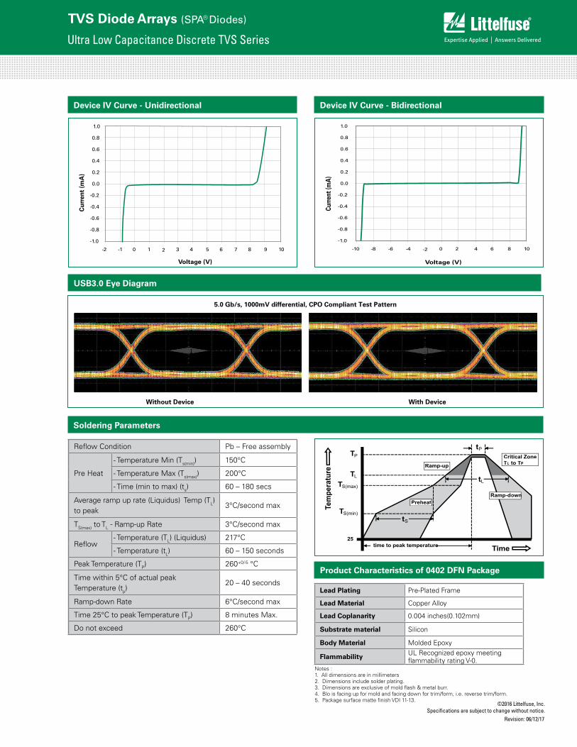
USB3.0 Eye Diagram
Without Device With Device
5.0 Gb/s, 1000mV differential, CPO Compliant Test Pattern
Disclaimer Notice - Information furnished is believed to be accurate and reliable. However, users should independently evaluate the suitability of and test each product selected for their own applications. Littelfuse products are not designed for, and may not be used in, all applications. Read complete Disclaimer Notice at www.littelfuse.com/disclaimer-electronics.