2020-2021 Microchip Technology Inc. DS20006425C-page 1 MX77 Features • Generates Differential or Single-Ended Output • 85 fs (typ.) Phase Jitter @ 156.25 MHz (12 kHz to 20 MHz) • 80 fs (typ.) Phase Jitter @ 312.5 MHz (12 kHz to 20 MHz) • 12 On-Chip Power Supply Regulators for Excellent Power Supply Noise Immunity >-75dB Suppression • Integrated Quartz Crystal for Superior Reliability, Noise/Jitter Performance • Excellent Close in Phase Noise • Independently Programmable Output Logic: - Output Logic: LVPECL, LVDS, HCSL, LVCMOS • 2.5V to 3.3V Operating Power Supply • Industrial Temperature Range, –40°C to +85°C • Green, RoHS, and PFOS Compliant QFN • Industry Standard 6-Pin, 5 mm x 7 mm Package • Moisture Sensitivity Level (MSL): Level-1 Applications • 10/40/100/400 Gigabit Ethernet - (GMII) • SONET/SDH • PCI-Express Gen 1/2/3/4/5/6 Compliant • CPRI/OBSAI - Wireless Base Station • Fibre Channel • HDMI/HDTV 4K/8k • DIMM (DDR2-3-4/AMB) • High Speed ADC/DAC • Optical Network (OTN, DCI) General Description The MX77XXXX series are a family of PLL clock oscillators plus integrated quartz crystal that achieves ultra-low phase jitter (<90 fs RMS typical, 12.5 MHz up to 875 MHz). The output can be programmed to LVPECL, LVDS, HCSL, or LVCMOS logic. The MX77 is packaged in a standard 6-pin LGA. Block Diagram PLL ÷ XO Q /Q VDD Power Rail Regulation OTP MEMORY VSS VDD OE Ultra-Low Jitter Clock Oscillator with Integrated Quartz Crystal
Transcript
2020-2021 Microchip Technology Inc. DS20006425C-page 1
The MX77XXXX series are a family of PLL clockoscillators plus integrated quartz crystal that achievesultra-low phase jitter (<90 fsRMS typical, 12.5 MHz up to875 MHz).
The output can be programmed to LVPECL, LVDS,HCSL, or LVCMOS logic.
The MX77 is packaged in a standard 6-pin LGA.
Block Diagram
PLL ÷XO Q/Q
VDD Power Rail Regulation
OTP MEMORY
VS
S
VD
DO
E
Ultra-Low Jitter Clock Oscillator with Integrated Quartz Crystal
MX77
DS20006425C-page 2 2020-2021 Microchip Technology Inc.
Supply Voltage (VDD)....................................................................................................................... +2.375V to +3.465V
† Notice: Stresses above those listed under “Absolute Maximum Ratings” may cause permanent damage to the device.This is a stress rating only and functional operation of the device at those or any other conditions above those indicatedin the operational sections of this specification is not intended. Exposure to maximum rating conditions for extendedperiods may affect device reliability.
†† Notice: The data sheet limits are not guaranteed if the device is operated beyond the operating ratings.
DC ELECTRICAL CHARACTERISTICSElectrical Characteristics: Unless otherwise indicated, typical values are for TA = +25°C. The min. and max. values are for –40°C ≤ TA ≤ +85°C.
Parameters Symbol Min. Typ. Max. Units Conditions
Supply Voltage VDD2.375 2.5 2.625
V2.5V Operation
3.135 3.3 3.465 3.3V Operation
Current Consumption
IDD — 135 180 mA @3.3V
LVPECL DC ELECTRICAL CHARACTERISTICSElectrical Characteristics: VDD = 3.3V ±5% to 2.5V ±5%, TA = –40°C to +85°C, unless otherwise noted. RL = 50Ω to VDDO – 2V.
Parameter Symbol Min. Typ. Max. Units Condition
Output High Voltage VOH VDDO – 1.35 VDDO – 1.01 VDDO – 0.8 V 50Ω to VDDO – 2V
Output Low Voltage VOL VDDO – 2 VDDO – 1.78 VDDO – 1.6 V 50Ω to VDDO – 2V
Peak-to-Peak Output Voltage VSWING 0.65 0.77 0.95 V Figure 5-3, Figure 5-6
LVDS DC ELECTRICAL CHARACTERISTICSElectrical Characteristics: VDD = 3.3V ±5% to 2.5V ±5%, TA = –40°C to +85°C, unless otherwise noted. RL = 100Ω between Q and /Q.
Common Mode Voltage VCM 1.125 1.2 1.375 V Figure 5-3, Figure 5-8
Output High Voltage VOH 1.248 1.375 1.602 V Figure 5-3, Figure 5-8
Output Low Voltage VOL 0.898 1.025 1.252 V Figure 5-3, Figure 5-8
2020-2021 Microchip Technology Inc. DS20006425C-page 3
MX77
HCSL DC ELECTRICAL CHARACTERISTICSElectrical Characteristics: VDD = 3.3V ±5% to 2.5V ±5%, TA = –40°C to +85°C, unless otherwise noted. RL = 50Ω to VSS.
Parameter Symbol Min. Typ. Max. Units Condition
Output High Voltage VOH 660 700 850 mV Figure 5-3, Figure 5-7
AC ELECTRICAL CHARACTERISTICSElectrical Characteristics: VDD = 3.3V ±5% to 2.5V ±5%, VDD = 3.3V ±5%, VDDO1/2 = 3.3V ±5% or 2.5V ±5%;TA = –40°C to +85°C.
Parameter Symbol Min. Typ. Max. Units Condition
Output Frequency FOUT12.5 — 875 MHz LVPECL, LVDS, HCSL
12.5 — 400 MHz LVCMOS
Output Rise/Fall Time Note 1
tR/tF
85 135 350
ps
LVPECL output
85 140 300 LVDS output
175 200 400 HCSL output
100 200 400LVCMOS output (default drive)
Output Duty Cycle ODC45 50 55 % All output frequencies
48 50 52 % < 450 MHz output frequencies
PLL Lock Time TLOCK — 5 20 ms Time from 90% VDD
RMS Phase Jitter Note 2, Figure 5-5
tJIT(Φ) —85 —
fs
156.250 MHz, Integration range (12 kHz - 20 MHz)
85 —156.250 MHz, Integration range (1.875 MHz - 20 MHz)
Note 1: See Figure 5-4.
2: All phase noise measurements were taken with an Agilent 5052B phase noise system.
3: The CMOS driver can deliver usable waveforms up to ~ 600 MHz under light loading and CL below 5 pf. Careful attention to signal integrity, transmission line design, VIA’s and signal termination must be fol-lowed. VIA design is very important and has the most effect on the waveform.
MX77
DS20006425C-page 4 2020-2021 Microchip Technology Inc.
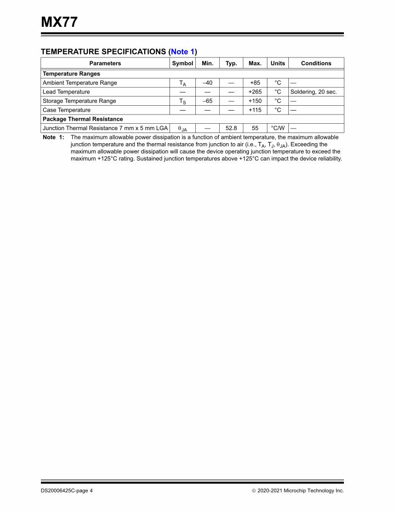
TEMPERATURE SPECIFICATIONS (Note 1)
Parameters Symbol Min. Typ. Max. Units Conditions
Temperature Ranges
Ambient Temperature Range TA –40 — +85 °C —
Lead Temperature — — — +265 °C Soldering, 20 sec.
Storage Temperature Range TS –65 — +150 °C —
Case Temperature — — — +115 °C —
Package Thermal Resistance
Junction Thermal Resistance 7 mm x 5 mm LGA JA — 52.8 55 °C/W —
Note 1: The maximum allowable power dissipation is a function of ambient temperature, the maximum allowable junction temperature and the thermal resistance from junction to air (i.e., TA, TJ, JA). Exceeding the maximum allowable power dissipation will cause the device operating junction temperature to exceed the maximum +125°C rating. Sustained junction temperatures above +125°C can impact the device reliability.
2020-2021 Microchip Technology Inc. DS20006425C-page 5
MX77
2.0 PIN DESCRIPTIONS
The descriptions of the pins are listed in Table 2-1.
TABLE 2-1: PIN FUNCTION TABLE
Pin Number
Pin Name Pin Type Pin Level Description
1 OE I, (SE) LVCMOSOutput Enable, Disable to tri-state(on-chip 75 kΩ pull-up)
2 NC — —No ConnectNo internal connections to the ASIC are made
3 GND-VSS PWR — Power Supply Ground
4 Q1O, (DIF/SE)
LVPECL, LVDS HCSL, LVCMOS
(Q only
Differential /SE Clock Output (LVCMOS)5 Q1/
6 VDD PWR — Power Supply
TABLE 2-2: TRUTH TABLE
Output Enable OE = Pin 1 OE Default State
Enable Pin option B —
Output Logic Type
A= PECLB=LVDSC=CMOSD=HCSL
Active high
F=PECLG=LVDSH=CMOSJ=HCSL
Active low
MX77
DS20006425C-page 6 2020-2021 Microchip Technology Inc.
3.0 PHASE NOISE PERFORMANCE
FIGURE 3-1: 150.0000 MHz, HCSL, Integration Range 12 kHz to 20 MHz: 77.6 fsRMS.
FIGURE 3-2: 156.250 MHz, LVPECL, Integration Range 12 kHz to 20 MHz: 82 fsRMS.
Note: The graphs and tables provided following this note are a statistical summary based on a limited number ofsamples and are provided for informational purposes only. The performance characteristics listed hereinare not tested or guaranteed. In some graphs or tables, the data presented may be outside the specifiedoperating range (e.g., outside specified power supply range) and therefore outside the warranted range.
2020-2021 Microchip Technology Inc. DS20006425C-page 7
MX77
FIGURE 3-3: 312.500 MHz, LvPecl. Integration Range 12 kHz to 20 MHz: 83 fsRMS.
FIGURE 3-4: 322.265625 MHz, LVPECL Integration Range 12 kHz to 20 MHz: 75 fsRMS.
MX77
DS20006425C-page 8 2020-2021 Microchip Technology Inc.
FIGURE 3-5: 625.0000 MHz, HCSL Integration Range 12 kHz to 20 MHz: 72.7 fsRMS.
2020-2021 Microchip Technology Inc. DS20006425C-page 9
MX77
4.0 KEY PROGRAMMABLE PARAMETERS
4.1 Frequency Settings for One PLL and One Output Bank
FIGURE 4-1: Frequency Settings for PLL and Output Bank.
The crystal reference frequency is integer multiplied tofall within the VCO capture range and the post dividersdivide the VCO back down to the required frequency.
The VCO has a range of 2875 MHz to 3540 MHz.
Counters M and P0 have a range of 4 to 259.
Counter P1 has a range of 1 to 16.
EQUATION 4-1:
EQUATION 4-2:
4.2 Output Logic Programming
The output can be programmed to one of four logictypes, LVPECL, LVDS, HCSL, and LVCMOS.
All logic types are differential except LVCMOS. ForLVCMOS, only the true channel of the output pair isenabled, and the complementary channel is disabled,HiZ. With LVCMOS there is also an output drive setting,3 bits, that can be set to adjust edge rate.
These bits are set at the factory and depend oncustomer application, frequency, loading and EMI.
The default setting is 4.PLLVCO ÷(P1)XO
VDD Power Rail Regulation
OTP MEMORY
VS
S
VD
DO
E
Q/Q÷(P2)
FVCO REF M=
Q1 FVCO P0 P1 =
MX77
DS20006425C-page 10 2020-2021 Microchip Technology Inc.
5.0 APPLICATION INFORMATION
5.1 Output Traces
Design the output signal traces according to the outputlogic requirements, terminations, etc. These are highedge rate signals so care must be taken in the PCBlayout/traces, use best SI practices. If LVCMOS isunterminated at the destination device and the tracelength is 1/4 λ or longer add a ~30Ω resistor in serieswith the oscillator output and as close as possible to theoutput pin. Then start a 50Ω trace to the clockconsumer device.
For differential traces you can either use a differentialdesign or two separate 50Ω traces. For EMI reasons, itis better to use a balanced differential transmission linedesign.
LVDS can be AC-coupled or DC-coupled to itstermination.
5.2 Power Supply Filtering Recommendations
FIGURE 5-1: Recommended Power Supply Filtering.
• Use the power supply filtering shown in Figure 5-1 for VDD.
• Connect VSS (GND) pin directly to the ground power plane.
• Recommended ferrite bead properties are 80Ω to 240Ω impedance @100 MHz and >250 mA saturation current.
• To improve power supply filtering beyond what a ferrite bead Pi filter can provide, the Ripple Blocker™ provides a solution. MIC94300 or MIC94310 are recommended parts. The filter circuit with Ripple Blocker is shown in Figure 5-2 and can be used along with any of the above VDD sections except VDDO.
FIGURE 5-2: Filter Circuit with Ripple Blocker.
FIGURE 5-3: Duty Cycle Timing.
FIGURE 5-4: All Outputs Rise/Fall Time.
FIGURE 5-5: RMS Phase/Noise/Jitter.
FIGURE 5-6: LVPECL Output Test Circuit.
FIGURE 5-7: HCSL Output Test Circuit.
Vdd Plane0.5
10μF 0.047μF 0.01μF 4.7nF
VDD Pin6
FB
2020-2021 Microchip Technology Inc. DS20006425C-page 11
MX77
FIGURE 5-8: LVDS Output Test Circuit.
FIGURE 5-9: LVCMOS Output Test Circuit.
5.3 HCSL Source Terminated Per JESD8-18A
FIGURE 5-10: 85Ω Differential Transmission Line.
FIGURE 5-11: 100Ω Differential Transmission Line.
HCSLOutput
HCSLInput
Two 42.5 traces /85 Differential traceRS
RS
RT
RT
RS = 27
RT = 43
HCSLOutput
HCSLInput
Two 50 traces /100 Differential traceRS
RS
RT
RT
RS = 33
RT = 49.9
MX77
DS20006425C-page 12 2020-2021 Microchip Technology Inc.
Environmental Specifications
TABLE 5-1: ENVIRONMENTAL SPECIFICATIONS
Parameter Specification
Thermal Shock MIL-STD-883, Method 1011, Condition A
Moisture Resistance MIL-STD-883, Method1004
Mechanical Shock MIL-STD-883, Method 2022, Condition C
Mechanical Vibration MIL-STD-883, Method 2007, Condition B
2020-2021 Microchip Technology Inc. DS20006425C-page 13
MX77
6.0 PACKAGING INFORMATION
6.1 Package Marking Information
XXXXXXX
Example6-Pin LGA*
MX775AB2333 †WNNN †
5 mm x 7 mm
XXXXXXXX A156M250
Legend: XX...X Product code, customer-specific information, or frequency in MHz without printed decimal pointY Year code (last digit of calendar year)YY Year code (last 2 digits of calendar year)WW Week code (week of January 1 is week ‘01’)NNN Alphanumeric traceability code Pb-free JEDEC® designator for Matte Tin (Sn)* This package is Pb-free. The Pb-free JEDEC designator ( )
can be found on the outer packaging for this package.
, , Pin one index is identified by a dot, delta up, or delta down (trianglemark).
Note: In the event the full Microchip part number cannot be marked on one line, it willbe carried over to the next line, thus limiting the number of availablecharacters for customer-specific information. Package may or may not includethe corporate logo.
Underbar (_) and/or Overbar (‾) symbol may not be to scale.
3e
3e
MX77
DS20006425C-page 14 2020-2021 Microchip Technology Inc.
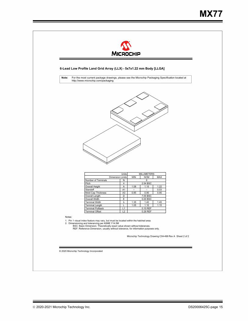
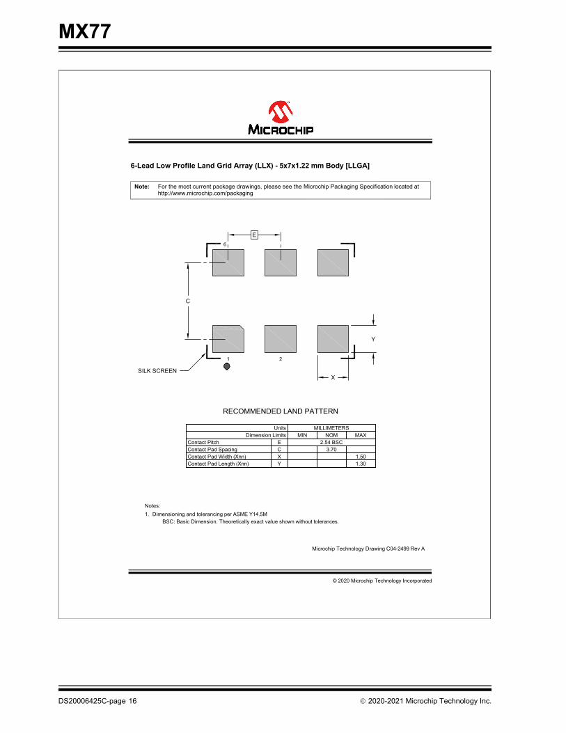
6-Lead Low 7 mm x 5 mm LLGA Package Outline and Recommended Land Pattern
2020-2021 Microchip Technology Inc. DS20006425C-page 17
MX77
APPENDIX A: REVISION HISTORY
Revision A (October 2020)
• Initial creation of MX77 Microchip data sheet DS20006425A.
Revision B (December 2020)
• Removed the Frequency Table that was under Standard Base Modules.
• Updated image for package marking under Section 6.0 “Packaging Information”.
• Also updated the table for Product Identification System.
Revision C (March 2021)
• Corrected Stability option in the Product Identifica-tion System.
MX77
DS20006425C-page 18 2020-2021 Microchip Technology Inc.
NOTES:
2020-2021 Microchip Technology Inc. DS20006425C-page 19
MX77
PRODUCT IDENTIFICATION SYSTEM
To order or obtain information, e.g., on pricing or delivery, contact your local Microchip representative or sales office.
PART NO. XX
Media TypeDevice
Device: MX77: Ultra-Low Jitter Clock oscillator with Integrated Quartz Crystal
Revision(Auto Generated after Selecting Output Fre-quency)
5A, 5B, 5C, 5D, 5E, 6A, 6B, 6C
Stability: B = ±50 ppm/20 ppm (–40°C to +85°C)
Output Logic A = PECLB = LVDSC = CMOSD = HCSL
Output Frequency: xxxMxxx = Generated by ClockWorks® Configurator
Shipping T = 43/TubeR = 1,000/Reel
X
Stability
X
Output Logic
XXXMXXX
Output
Note 1: Tape and Reel identifier only appears in the catalog part number description. This identifier is used for ordering purposes and is not printed on the device package. Check with your Microchip Sales Office for package availability with the Tape and Reel option.
Examples:
a) MX775ABB156M250T:
156.250 MHz LVDS Single Output,6-Lead LGA, –40°C to +85°C Tem-perature Range, ±50 ppm Stability,43/Tube
b) MX776ABD156M250R:
156.250 MHz HCSL Single Output,6-Lead LGA, –40°C to +85°C Tem-perature Range, ±50 ppm Stability,1,000/Reel
Frequency
Please visit http://clockworks.microchip.com/timing to select a combination ofoptions to customize your product, print a specific data sheet and order samples.
DS20006425C-page 20 2020-2021 Microchip Technology Inc.
NOTES:
Note the following details of the code protection feature on Microchip devices:
• Microchip products meet the specifications contained in their particular Microchip Data Sheet.
• Microchip believes that its family of products is secure when used in the intended manner and under normal conditions.
• There are dishonest and possibly illegal methods being used in attempts to breach the code protection features of the Microchip devices. We believe that these methods require using the Microchip products in a manner outside the operating specifications contained in Microchip's Data Sheets. Attempts to breach these code protection features, most likely, cannot be accomplished without violating Microchip's intellectual property rights.
• Microchip is willing to work with any customer who is concerned about the integrity of its code.
• Neither Microchip nor any other semiconductor manufacturer can guarantee the security of its code. Code protection does not mean that we are guaranteeing the product is "unbreakable." Code protection is constantly evolving. We at Microchip are committed to continuously improving the code protection features of our products. Attempts to break Microchip's code protection feature may be a violation of the Digital Millennium Copyright Act. If such acts allow unauthorized access to your software or other copyrighted work, you may have a right to sue for relief under that Act.
Information contained in this publication is provided for the solepurpose of designing with and using Microchip products. Infor-mation regarding device applications and the like is providedonly for your convenience and may be superseded by updates.It is your responsibility to ensure that your application meetswith your specifications.
THIS INFORMATION IS PROVIDED BY MICROCHIP "AS IS".MICROCHIP MAKES NO REPRESENTATIONS OR WAR-RANTIES OF ANY KIND WHETHER EXPRESS OR IMPLIED,WRITTEN OR ORAL, STATUTORY OR OTHERWISE,RELATED TO THE INFORMATION INCLUDING BUT NOTLIMITED TO ANY IMPLIED WARRANTIES OF NON-INFRINGEMENT, MERCHANTABILITY, AND FITNESS FOR APARTICULAR PURPOSE OR WARRANTIES RELATED TOITS CONDITION, QUALITY, OR PERFORMANCE.
IN NO EVENT WILL MICROCHIP BE LIABLE FOR ANY INDI-RECT, SPECIAL, PUNITIVE, INCIDENTAL OR CONSEQUEN-TIAL LOSS, DAMAGE, COST OR EXPENSE OF ANY KINDWHATSOEVER RELATED TO THE INFORMATION OR ITSUSE, HOWEVER CAUSED, EVEN IF MICROCHIP HASBEEN ADVISED OF THE POSSIBILITY OR THE DAMAGESARE FORESEEABLE. TO THE FULLEST EXTENTALLOWED BY LAW, MICROCHIP'S TOTAL LIABILITY ONALL CLAIMS IN ANY WAY RELATED TO THE INFORMATIONOR ITS USE WILL NOT EXCEED THE AMOUNT OF FEES, IFANY, THAT YOU HAVE PAID DIRECTLY TO MICROCHIPFOR THE INFORMATION. Use of Microchip devices in life sup-port and/or safety applications is entirely at the buyer's risk, andthe buyer agrees to defend, indemnify and hold harmlessMicrochip from any and all damages, claims, suits, or expensesresulting from such use. No licenses are conveyed, implicitly orotherwise, under any Microchip intellectual property rightsunless otherwise stated.
2020-2021 Microchip Technology Inc.
For information regarding Microchip’s Quality Management Systems, please visit www.microchip.com/quality.
TrademarksThe Microchip name and logo, the Microchip logo, Adaptec, AnyRate, AVR, AVR logo, AVR Freaks, BesTime, BitCloud, chipKIT, chipKIT logo, CryptoMemory, CryptoRF, dsPIC, FlashFlex, flexPWR, HELDO, IGLOO, JukeBlox, KeeLoq, Kleer, LANCheck, LinkMD, maXStylus, maXTouch, MediaLB, megaAVR, Microsemi, Microsemi logo, MOST, MOST logo, MPLAB, OptoLyzer, PackeTime, PIC, picoPower, PICSTART, PIC32 logo, PolarFire, Prochip Designer, QTouch, SAM-BA, SenGenuity, SpyNIC, SST, SST Logo, SuperFlash, Symmetricom, SyncServer, Tachyon, TimeSource, tinyAVR, UNI/O, Vectron, and XMEGA are registered trademarks of Microchip Technology Incorporated in the U.S.A. and other countries.
AgileSwitch, APT, ClockWorks, The Embedded Control Solutions Company, EtherSynch, FlashTec, Hyper Speed Control, HyperLight Load, IntelliMOS, Libero, motorBench, mTouch, Powermite 3, Precision Edge, ProASIC, ProASIC Plus, ProASIC Plus logo, Quiet-Wire, SmartFusion, SyncWorld, Temux, TimeCesium, TimeHub, TimePictra, TimeProvider, WinPath, and ZL are registered trademarks of Microchip Technology Incorporated in the U.S.A.
Adjacent Key Suppression, AKS, Analog-for-the-Digital Age, Any Capacitor, AnyIn, AnyOut, Augmented Switching, BlueSky, BodyCom, CodeGuard, CryptoAuthentication, CryptoAutomotive, CryptoCompanion, CryptoController, dsPICDEM, dsPICDEM.net, Dynamic Average Matching, DAM, ECAN, Espresso T1S, EtherGREEN, IdealBridge, In-Circuit Serial Programming, ICSP, INICnet, Intelligent Paralleling, Inter-Chip Connectivity, JitterBlocker, maxCrypto, maxView, memBrain, Mindi, MiWi, MPASM, MPF, MPLAB Certified logo, MPLIB, MPLINK, MultiTRAK, NetDetach, Omniscient Code Generation, PICDEM, PICDEM.net, PICkit, PICtail, PowerSmart, PureSilicon, QMatrix, REAL ICE, Ripple Blocker, RTAX, RTG4, SAM-ICE, Serial Quad I/O, simpleMAP, SimpliPHY, SmartBuffer, SMART-I.S., storClad, SQI, SuperSwitcher, SuperSwitcher II, Switchtec, SynchroPHY, Total Endurance, TSHARC, USBCheck, VariSense, VectorBlox, VeriPHY, ViewSpan, WiperLock, XpressConnect, and ZENA are trademarks of Microchip Technology Incorporated in the U.S.A. and other countries.
SQTP is a service mark of Microchip Technology Incorporated in the U.S.A.The Adaptec logo, Frequency on Demand, Silicon Storage Technology, and Symmcom are registered trademarks of Microchip Technology Inc. in other countries.GestIC is a registered trademark of Microchip Technology Germany II GmbH & Co. KG, a subsidiary of Microchip Technology Inc., in other countries. All other trademarks mentioned herein are property of their respective companies.


![ECEN620: Network Theory Broadband Circuit Design Fall 2019ece.tamu.edu/~spalermo/ecen620/lecture07_ee620_vcos.pdf• VCO Jitter 23. Oscillator Noise 24 Jitter [McNeill] Phase Noise](https://static.documents.pub/doc/80x56/5eb0f0afdb23476d411ded00/ecen620-network-theory-broadband-circuit-design-fall-spalermoecen620lecture07ee620vcospdf.jpg)


