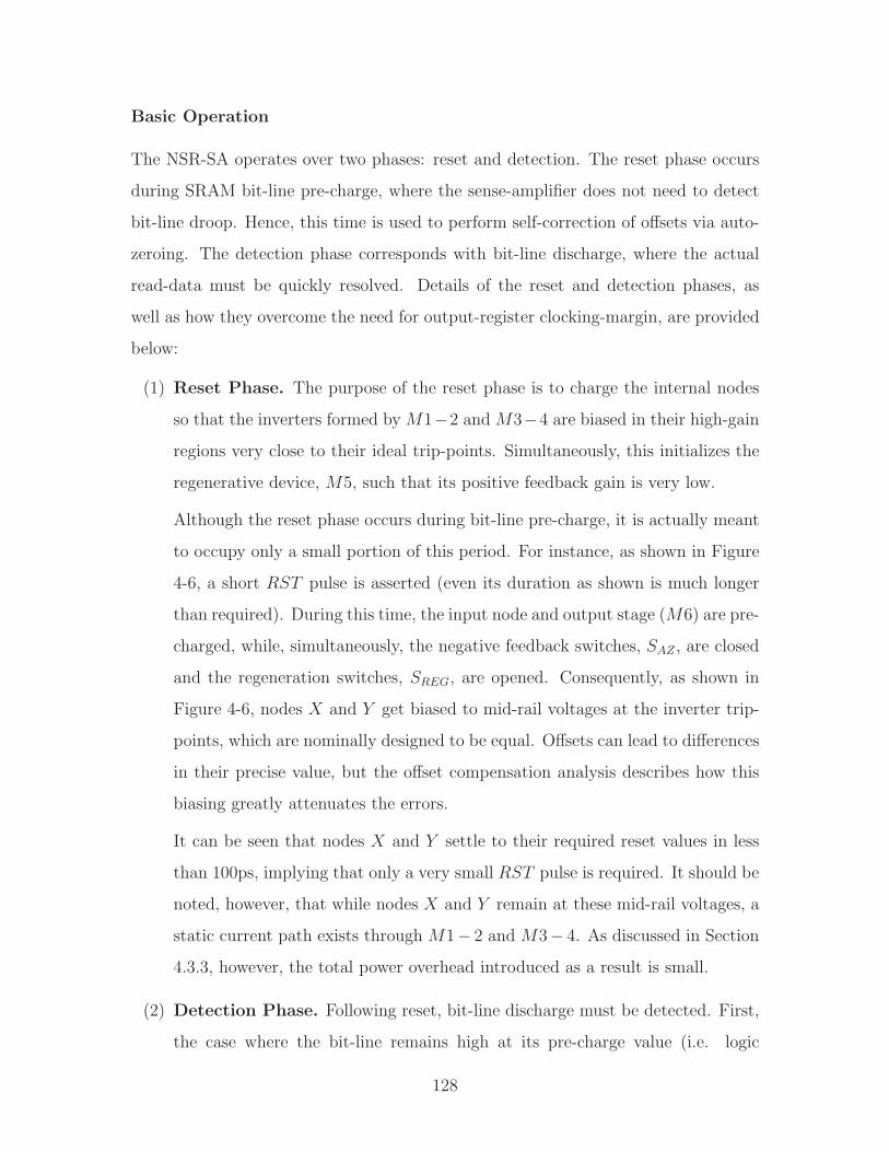
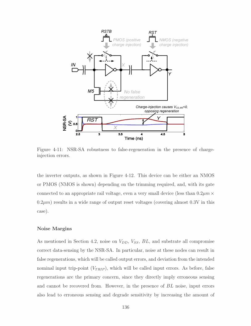
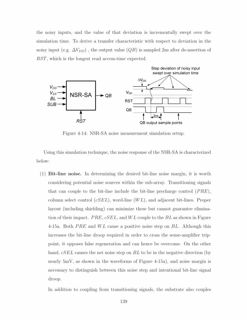
Ultra-Low-Power SRAM Design In High Variability Advanced CMOS by Naveen Verma Submitted to the Department of Electrical Engineering and Computer Science in partial fulfillment of the requirements for the degree of Doctor of Philosophy at the MASSACHUSETTS INSTITUTE OF TECHNOLOGY June 2009 c Massachusetts Institute of Technology 2009. All rights reserved. Author .............................................................. Department of Electrical Engineering and Computer Science May 5, 2009 Certified by .......................................................... Anantha P. Chandrakasan Joseph F. and Nancy P. Keithley Professor of Electrical Engineering Thesis Supervisor Accepted by ......................................................... Terry P. Orlando Chairman, Department Committee on Graduate Theses
Transcript
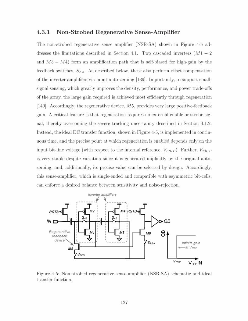
Ultra-Low-Power SRAM Design In High
Variability Advanced CMOS
by
Naveen Verma
Submitted to the Department of Electrical Engineering and ComputerScience
in partial fulfillment of the requirements for the degree of
Doctor of Philosophy
at the
MASSACHUSETTS INSTITUTE OF TECHNOLOGY
June 2009
c! Massachusetts Institute of Technology 2009. All rights reserved.
Submitted to the Department of Electrical Engineering and Computer Scienceon May 5, 2009, in partial fulfillment of the
requirements for the degree ofDoctor of Philosophy
Abstract
Embedded SRAMs are a critical component in modern digital systems, and their roleis preferentially increasing. As a result, SRAMs strongly impact the overall power,performance, and area, and, in order to manage these severely constrained trade-o!s,they must be specially designed for target applications. Highly energy-constrainedsystems (e.g. implantable biomedical devices, multimedia handsets, etc.) are animportant class of applications driving ultra-low-power SRAMs.
This thesis analyzes the energy of an SRAM sub-array. Since supply- and threshold-voltage have a strong e!ect, targets for these are established in order to optimizeenergy. Despite the heavy emphasis on leakage-energy, analysis of a high-density256"256 sub-array in 45nm LP CMOS points to two necessary optimizations: (1) ag-gressive supply-voltage reduction (in addition to Vt elevation), and (2) performanceenhancement. Important SRAM metrics, including read/write/hold-margin and read-current, are also investigated to identify trade-o!s of these optimizations.
Based on the need to lower supply-voltage, a 0.35V 256kb SRAM is demonstratedin 65nm LP CMOS. It uses an 8T bit-cell with peripheral circuit-assists to improvewrite-margin and bit-line leakage. Additionally, redundancy, to manage the increas-ing impact of variability in the periphery, is proposed to improve the area-o!settrade-o! of sense-amplifiers, demonstrating promise for highly advanced technologynodes. Based on the need to improve performance, which is limited by density con-straints, a 64kb SRAM, using an o!set-compensating sense-amplifier, is demonstratedin 45nm LP CMOS with high-density 0.25µm2 bit-cells. The sense-amplifier is re-generative, but non-strobed, overcoming timing uncertainties limiting performance,and it is single-ended, for compatibility with 8T cells. Compared to a conventionalstrobed sense-amplifier, it achieves 34% improvement in worst-case access-time and4x improvement in the standard deviation of the access-time.
Thesis Supervisor: Anantha P. ChandrakasanTitle: Joseph F. and Nancy P. Keithley Professor of Electrical Engineering
3
4
Acknowledgments
MIT is truly a unique and wonderful place on this earth. For a new graduate student,
as I once was, it can easily be too wonderful and too big. The only way to realize your
place at MIT is through the guidance, encouragement, support, and friendship of an
outstanding advisor like Prof. Anantha Chandrakasan. First and foremost, I thank
Anantha. When I arrived here, I was not sure what, if anything, I could accomplish.
Anantha, convinced me, by always expecting more from me, by always challenging me,
and by supporting me through every research endeavor, that I could be a contributing
member of this great community. His lessons for me have gone far beyond circuits;
he has taught me to be a critical, sincere, cooperative, and respectful researcher.
Anantha works firstly for his students, and I have learned more by watching him than
I ever will from reading volumes of journals. As I proceed in my career, Anantha will
always play an important role; he has given me something to strive for technically
and personally. Thank you, Anantha, for your always strong support and guidance.
I am eternally grateful to my thesis committee members, Prof. Charlie Sodini
and Prof. Duane Boning. Every researcher o!ers his work to the community hoping
it is received by someone. To be able to discuss my work with such outstanding
researchers as Charlie and Duane is the greatest honor of my career. Charlie and
Duane have given this thesis a level of attention that has made the e!ort more than
worthwhile. Thank you for your feedback and support, which has always aimed to
make this thesis better. Because of your input, I am much prouder of this work, and
after the many years it has consumed, that means a lot!
There are several faculty at MIT who have had a profound impact on me both
technically and non-technically. I am extremely grateful to Prof. Harry Lee, who’s
mastery of circuits, and the ability to make that mastery accessible, has inspired me
to study every last aspect of my field. I am grateful to Prof. Al Oppenheim who,
by example, has shown me the impact that excellence in teaching can have and the
level of dedication that must applied. I thank Prof. John Guttag for encouraging me
to enthusiastically and intrepidly venture into new fields to seek out for myself how I
5
might broaden my contributions. Finally, I thank Prof. Joel Dawson for showing me
that a newbie can have as big an impact as anyone, and he can do so without strain
or tension, smiling all the way.
By far the most rewarding aspect of MIT has been the people I have been so
fortunate to interact with. First, I must thank Margaret, who has repeatedly rescued
me from overloads and crises. Margaret keeps ananthagroup running straight even
when us students have accidentally gone in the wrong direction! Technically, the most
fun I have ever had was discussing, debating, and pondering with Brian Ginsburg
on matters of how to design an ADC (yes, many of the problems we hotly contested
were already solved, but sometimes re-inventing the wheel is an unmatchable learning
exercise!). I will always remember those years spent with Brian twisting my brain
in front a white-board. Past members of ananthagroup, especially Benton Calhoun
and David Wentzlo!, showed me the ropes of being a graduate student. This, as
they taught me, involves more than just tape-outs and paper deadlines; it involves
lunch-time business plans, political/social debates, “useless” riddles and anecdotes,
and most of all, laughs wherever they can be found. Also in this category are Alice
Wang, Frank Honore, Fred Lee, and Raul Blazquez.
I am privileged to have the current members of ananthagroup around me every-
day. I am especially grateful for the technical discussions and collaborations of Joyce
Kwong, Yogesh Ramadass, and Nigel Drego (I will have more to say about these last
two clowns shortly). I must thank my good friend Manish Bhardwaj, not just for
his technical feedback but also for his support and encouragement, which was always
on-hand when I needed it most (like when he put in a late night of chip testing with
me to get results that were due the previous week!). Daniel Finchelstein, Denis Daly,
and I arrived at MIT together, and I have had these two to lean on throughout my
time here. They are the best fellow travellers one can hope for on this sort of journey,
and I am grateful for their friendship the whole way through. It is also inspiring to
see the newer students in the group, Vivienne Sze, Mahmut Ersin Sinangil, Patrick
Mercier, and Masood Qazi, excelling and indeed becoming leaders.
I have especially been looking forward to say something about my friend Ali Shoeb.
6
His hyperactivity and enthusiasm are the main reasons why I will continually seek to
expand and broaden my horizons beyond any narrow expertise I might have. Ali is
genuinely inspired, and he inspires me! Eugene Shih is more controlled, but he has
contributed equally to the fun I have had on the ninth flour of Building 32!
Thankfully, my experiences at MIT have actually gone far beyond MIT. I am
extremely grateful for the support and encouragement I have received from collabo-
rators at Texas Instruments. Most of all, Dennis Buss has been a champion of my
work throughout my Ph.D. years. His enthusiasm has been a constant driving force,
and he has spun miracles for me on more than one occasion to overcome the barriers
and hurdles that inevitably arise during research. I am also grateful to Ted Houston,
Wah-Kit Loh, Xiaowei Deng, Mike Clinton, Hugh Mair, and Alice Wang for their
constant support and feedback.
I am thankful to Intel for providing me with fellowship support during my Ph.D.
Even more importantly, Kevin Zhang of Intel has played a major role in how I have
approached SRAMs from the research perspective. In fact, much of the work in this
thesis has been inspired by his own research and the feedback he has been so generous
to me with. Kevin has been a constant supporter and a mentor who I will always
look to for stimulating discussions and input.
I am also thankful to Peter Holloway of National Semiconductor. It is much easier
to do research when one has the kind of support that Peter has given me throughout
my Ph.D. Peter has a unique perspective on circuits that is rooted in real-life; the
only way a novice like myself can appreciate such a perspective is through the very
intriguing and stimulating discussions I have had with him.
Completing a Ph.D. is far more than a test of technical execution. In fact, most
of all, it is a test of will and morale. For both of these I am eternally grateful to the
close friends I have made during my time here at MIT. Some of my most important
moments at MIT have been spent during co!ee-time with Nigel Drego and Yogesh
Ramadass. Here, we got to transfer our analysis skill to all of life’s great problems.
None of us knows if we ever came close or even began to solve any of these, but
we always returned from co!ee less stressed, more motivated, and of course slightly
7
more awake... any way you cut it co!ee-time is indispensible! Yogesh, Nigel, Vidya,
Anand, and Nammi are great friends, and we are truly blessed to be able to laugh,
lounge, and talk smack with them. The same, of course, goes for Daniel and Tarik
(and Minou!). Since I arrived here at MIT Raj, Ferdi, Federico, and Gabi have been
the rough-around-the-edges group with whom I could always be myself. This turns
out to be a critical outlet when the pressure begins mounting, as it frequently does
at MIT.
Finally, I come to my family, without whom nothing in my life, let alone my
research, could ever have been possible. Most of all, my hard work and sincere e!orts
are for Mom Ji and Dad Ji. I have always relied on your love and prayers to lift me
over obstacles. Of course, Vancouver is a continent away, but I have always felt you
here with me, and that has been the strength I have needed. This thesis is for both
of you. Thank you for your support, love, and blessings.
So far as e!ort put into this thesis is concerned, the first credit undoubtedly goes
my amazing wife Anita. Ana, you are the reason behind this accomplishment, and
your smile (and occasional craziness!) are the only rewards I hope for every day.
Thank you for your love and support. I love you with all my heart.
I am blessed to also have the support and love of a second set of parents. Mom
and Bug, thank you for your prayers, wishes, jokes, and love. I do not expect you to
read this thesis, but I do hope you realize the role you have played in supporting me
towards its completion. Thank you, once again, for your support, love, and blessings.
I am anxious to thank Angelee, Serena, and Jaimini. You three remind me that
there is a lot more to my life than whatever I am busy with today. Thank you for the
relief and lightening that your support and love always provides. This thesis truly
could not have been completed without the formidable force behind me that you three
have always been.
Similarly, Ang, Jason, and Connor, I know that you are always behind me and
Ana, and we are externally grateful for the love, laughs, and lessons (about leather-
backed turtles, etc.) that you have always provided.
Moore’s law of scaling [1] has been the most important driving force behind the
semiconductor industry. Scaling has directly or indirectly been the root cause of the
tremendous capabilities of today’s ICs and their ubiquitous use in nearly all modern
electronic systems. Though Gordon Moore recently amended his law to include a
much broader set of metrics associated with ICs [2], his basic statement pertains to
“components,” which literally implies number of transistors. Today, even as many
aspects of CMOS device scaling begin to saturate o! the exponential trend, density-
scaling remains a primary objective of the semiconductor industry [3]. In the face
of rapidly emerging limitations that are fundamental to continued device shrinking,
density-scaling enables circuit [4] and architecture level parallelism [5], providing a
means to achieve energy-e"ciency and performance improvements in lieu of of the
previous trends.
Embedded SRAMs provide a direct means of bringing the benefits of transistor-
level density-scaling to the circuit and architecture levels and are therefore vital to
this new model of IC scaling. Due to their regular structure and broad applicability to
so many digital systems, SRAMs are carefully designed as one of the lead components
during the development of new technology nodes, and they utilize highly specialized
and aggressive layout rules that address sub-resolution fabrication limitations. This
level of design attention has allowed SRAM bit-cells to follow density trends in-line
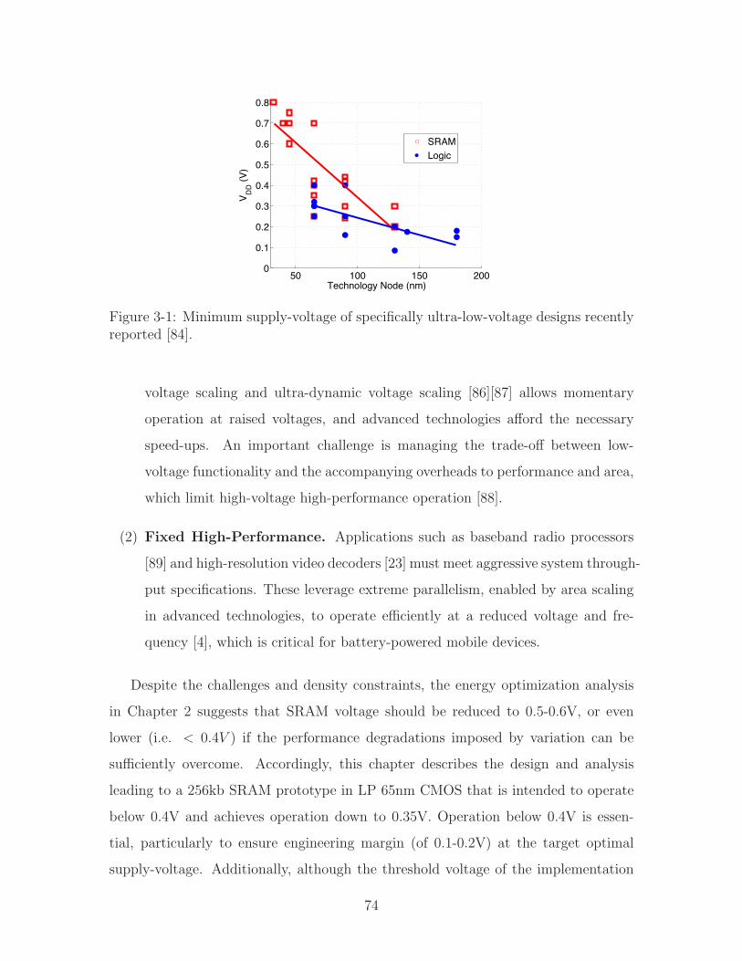
with the transistors themselves [6]. This is shown in Figure 1-1 where bit-cell areas
21
reported by Intel, IBM, TI, Sony, Renesas, and Samsung have been plotted versus
the technology node (represented by deployment year).
1998 2000 2002 2004 2006 200810-1
100
101
Year
Bit-C
ell S
ize
(µm
2 )32nm
(0.171µm2)
0.5x everytech. node
1998 2000 2002 2004 2006 200810-1
100
101
Year
Bit-C
ell S
ize
(µm
2 )32nm
(0.171µm2)
1998 2000 2002 2004 2006 200810-1
100
101
Year
Bit-C
ell S
ize
(µm
2 )32nm
(0.171µm2)
0.5x everytech. node
Figure 1-1: SRAM bit-cell density versus technology node showing cell density scal-ing in-line with transistor dimension scaling (every two years corresponds to a newtechnology node).
Accordingly, to benefit e"ciently from transistor density-scaling, modern digi-
tal architectures increasingly emphasize the use and integration of more and more
SRAMs [7][8]. The resulting consequence for low-power devices is that SRAMs oc-
cupy a dominating portion of the total die area and the total power consumption.
Figure 1-2 shows three state-of-the-art examples intended for increasingly low-power
applications: the Intel Core 2 processor targets mobile computing [9], the ARM1176JZ
processor targets hand-held computing [10], and the custom MSP430 microcontroller
targets remote wireless sensor and implantable biomedical computing [11]. The im-
portant trend observed here is that the SRAM (or memory) power becomes more and
more significant in increasingly low-power devices. The precise cause of this is dis-
cussed throughout the following chapters, but in the meantime, it is clear that SRAMs
are a fundamental platform component in the modern semiconductor industry, and
their power-consumption is a limiting factor.
An important evolution in the semiconductor industry is that, today, the appli-
cation space for integrated circuits is extremely broad, extending far beyond desktop
computing microprocessors to include ambient, remote, mobile, and implantable de-
22
Intel Core 2 (Penryn)6MB SRAM L2, 64kB RF L1
Power: 20%
ARM1176JZ 16kB SRAM cache
Power: 39%
Custom MSP43016kB SRAM cache
Power: 69%
• Mobile computing • Embedded/handheld • Implantable, sensor nets
Figure 1-2: Three example low-power applications demonstrating dominating areaand power-consumption of SRAMs: 45nm Intel Core 2 [9], 90nm ARM1176JZ (suit-able for iPhone application processor) [10], and 65nm custom MSP430 [11].
vices, to name a few. With regards to the constituent digital circuits, all of these
applications have vastly varying and highly stringent demands that require careful
design within the associated trade-o!s. In order to adhere to intense scaling trends,
SRAM design is also highly constrained, especially in the face of emerging limita-
tions ranging from device-level variability to system-level power consumption. Since
their impact on the overall system is so significant, and since their design is so con-
strained, modern embedded SRAMs must be developed with the application in mind
so that their own trade-o!s can be carefully managed. Generally speaking, SRAMs
are strongly subject to the power, performance, and density trade-o!s shown in Fig-
ure 1-3. The precise origins and e!ects of these trade-o!s are discussed throughout
the following chapters, but the overall implication is that improvement in one of the
dimensions strongly stresses the others. Of course, all three dimensions are impor-
tant to some degree in all applications; as a result, embedded SRAM design involves
making judicious compromises in order to support the most important system-specific
requirements. The focus of this work is to investigate techniques that improve the ba-
sic trade-o! in order to more e"ciently allow optimization of the parameters relevant
for the systems considered (these are discussed in more detail below). It is important
to note that although the illustration in Figure 1-3 indicates a simple inverse relation-
23
ship between power, performance, and density, in reality, the relationships are often
much more complicated, and, importantly, aggressive emphasis on one dimension,
such as power reduction, increases the opposition imposed by the other dimensions
with much higher intensity.
Performance
App.: • Desktop, server computing
• Advanced graphics, etc.
Trends: • Low-Vt devices
• Large bit-cells, short bit-lines
Density
App.: • Multimedia handsets
• Mobile, ubiquitous computing
Trends: • High-Vt devices
• Small bit-cells, long bit-lines
Low Power
App.: • Biomedical
• Wireless sensor networks
Trends: • High-Vt devices, low VMIN
• Medium bit-cells, short bit-lines
Figure 1-3: SRAM trade-o!s.
1.1 Ultra-Low-Power Embedded SRAM Applica-
tions
Since SRAMs must be specially designed with their application in mind, it is worth
considering the application constraints. This work specifically considers a number
of applications where power consumption, or, more generally, energy consumption,
is paramount. Of course, the SRAM challenges associated with achieving multi-
Giga-Hertz operation in high-performance applications, including desktop and server
computing, requires very targeted and innovative solutions as well [12][13][14]. How-
ever, a few of the highly energy-constrained applications that are the focus of this
work are considered below:
24
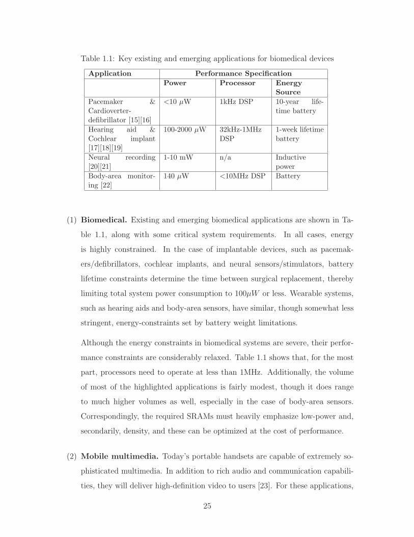
Table 1.1: Key existing and emerging applications for biomedical devices
Application Performance SpecificationPower Processor Energy
cessing, and communications capabilities can form networks, broadly referred
to as wireless sensor networks [24][25]. The applications for such devices include
industrial and automotive sensing [26], environment monitoring [27], structural
monitoring [28], and military surveillance/detection. Operation of such net-
works must be largely maintenance-free due to their use in remote or inaccessi-
ble physical locations. As a result, battery lifetime constraints are critical, and
the battery must be physically small to facilitate in-situ sensing in a broad range
of uses. Alternatively, to extend the lifetime of the sensor nodes, potentially in-
definitely, energy harvesting from the ambient environment can be leveraged as
long as occasional degradation in performance quality, depending on the ambi-
ent factors, can be tolerated. Nonetheless, the power consumption of the system
is limited by the harvesting capacity. Table 1.2 shows the power harvestable by
state-of-the-art energy harvesting devices, indicating a total power budget less
than 100µW for most of the sensor networks considered.
With regards to SRAM requirements, power consumption (both static and dy-
namic) is the primary concern, and, since most monitoring applications require
processing on low-speed signals, performance constraints are relaxed to the hun-
dreds of kilo-Hertz range. Since the nodes are meant to form high-density net-
works that are sacrificial after use, cost and density are also important concerns.
26
Table 1.2: Energy collecting and harvesting options [29][30][31][32]
Energy Source PerformanceThermoelectric 60 µW/cm3
Light 100 µW/cm2 (o"ce),100 mW/cm2 (direct light)
Vibration 4 µW/cm3 (human motion)Heel strike 10-700 mW (walking)Near-field inductive energy transfer 20 mW at 5 cm [33]Far-field inductive energy transfer 2 µW at 10 m [34]
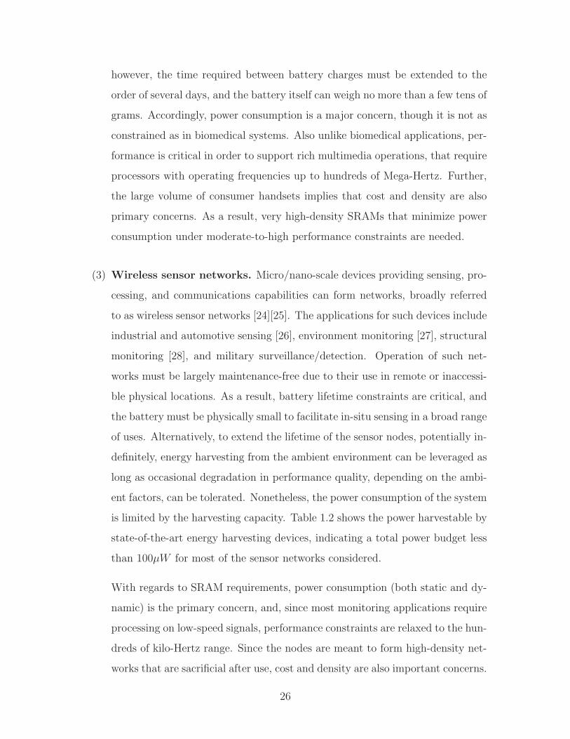
As with most digital systems, embedded SRAMs play a highly prominent role
in these energy-constrained applications. Also as before, they pose the most critical
limitation to the total power, performance, and area. Figure 1-4 shows an example of
a custom MSP430 microcontroller that specifically targets highly energy-constrained
biomedical and sensor applications [11]. Operating at its minimum energy point,
its on-chip SRAM cache consumes 69% of the total energy per operation, limits the
operating frequency (which is 1.7MHz for the SRAM at 0.5V), and, as shown, occupies
a dominating portion of the total area. Consequently, to enable the applications
described above, embedded SRAM is a critical area of focus.
128-kb SRAM
array
CPU
DC-
DC
Figure 1-4: Die photo of ultra-low-power low-voltage MSP430 microcontroller domi-nated by on-chip SRAM cache [11].
27
Energy Versus Power
For the applications discussed above, it is important to make the distinction between
energy consumption and power consumption. Ultimately, battery powered systems
are primarily limited by the energy the battery can provide. Energy harvesting sys-
tems typically use a battery (or other form of energy storage [35]) to bu!er the power
extracted from an ambient source [36], and, once again, average power consumption,
corresponding to total energy normalized over a time period, is the critical concern.
Performing any circuit operation requires energy, and, so, it is a fundamental metric
for battery operated and energy-harvesting systems.
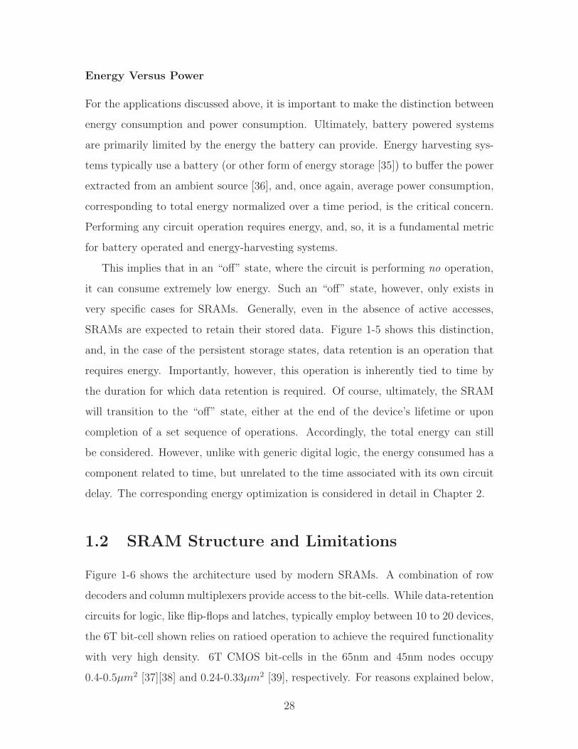
This implies that in an “o!” state, where the circuit is performing no operation,
it can consume extremely low energy. Such an “o!” state, however, only exists in
very specific cases for SRAMs. Generally, even in the absence of active accesses,
SRAMs are expected to retain their stored data. Figure 1-5 shows this distinction,
and, in the case of the persistent storage states, data retention is an operation that
requires energy. Importantly, however, this operation is inherently tied to time by
the duration for which data retention is required. Of course, ultimately, the SRAM
will transition to the “o!” state, either at the end of the device’s lifetime or upon
completion of a set sequence of operations. Accordingly, the total energy can still
be considered. However, unlike with generic digital logic, the energy consumed has a
component related to time, but unrelated to the time associated with its own circuit
delay. The corresponding energy optimization is considered in detail in Chapter 2.
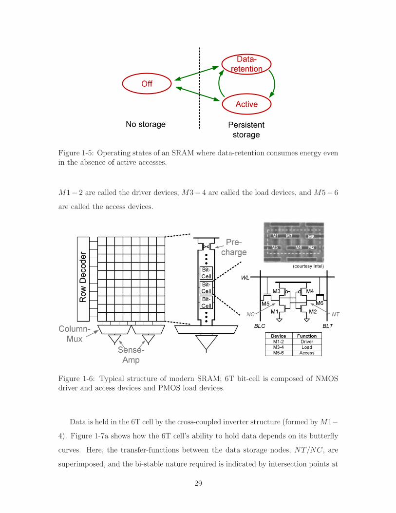
1.2 SRAM Structure and Limitations
Figure 1-6 shows the architecture used by modern SRAMs. A combination of row
decoders and column multiplexers provide access to the bit-cells. While data-retention
circuits for logic, like flip-flops and latches, typically employ between 10 to 20 devices,
the 6T bit-cell shown relies on ratioed operation to achieve the required functionality
with very high density. 6T CMOS bit-cells in the 65nm and 45nm nodes occupy
0.4-0.5µm2 [37][38] and 0.24-0.33µm2 [39], respectively. For reasons explained below,
28
Off
Data-
retention
Active
Persistent
storage
No storage
Figure 1-5: Operating states of an SRAM where data-retention consumes energy evenin the absence of active accesses.
M1# 2 are called the driver devices, M3# 4 are called the load devices, and M5# 6
are called the access devices.
Row
D
ecod
er
Column-
Mux
Sense-
Amp
Bit-
Cell
Bit-
Cell
Bit-
Cell
Pre-
charge
BLC BLT
M1 M2
M3 M4
M5 M6
NC NT
WL
Device
M1-2
M3-4
M5-6
Function
Driver
Load
Access
(courtesy Intel)
M1
M2
M3
M4M5
M6
Figure 1-6: Typical structure of modern SRAM; 6T bit-cell is composed of NMOSdriver and access devices and PMOS load devices.
Data is held in the 6T cell by the cross-coupled inverter structure (formed by M1#
4). Figure 1-7a shows how the 6T cell’s ability to hold data depends on its butterfly
curves. Here, the transfer-functions between the data storage nodes, NT/NC, are
superimposed, and the bi-stable nature required is indicated by intersection points at
29
valid logic “0” and “1” levels. Strictly speaking, read-access is a non-ratioed operation
where the bit-lines, BLT/BLC, are precharged, and, after word-line (WL) assertion,
the cell read current, IRD, which is generated by the driver and access devices, causes
a droop on one bit-line which can be sensed with respect to the other to quickly
decipher the accessed data. However, the transients on NT and NC can result in
loss of the bi-stable characteristic, and their worst-case impact can be analyzed by
assuming that BLT/BLC are clamped at VDD. The corresponding butterfly curves,
shown in Figure 1-7b, now have dangerously degraded lobes, quantified by the static
noise margin (SNM), which measures the diagonal length of the largest embedded
square [40]. An SNM less than zero implies the loss of one of the required intersection
points, indicating the cell’s inability to correctly retain the corresponding data state.
Hence, proper operation requires maintaining wide lobes, which depends on the driver
devices, M1 # 2, being much stronger than the access devices, M5 # 6.
0 0.2 0.4 0.6 0.8 10
0.1
0.2
0.3
0.4
0.5
0.6
0.7
0.8
0.9
1
NC, NT (V)
NT, N
C (V
)
NT NC
SNM
(a)
0 0.2 0.4 0.6 0.8 10
0.1
0.2
0.3
0.4
0.5
0.6
0.7
0.8
0.9
1
NC, NT (V)
NT, N
C (V
)
NT NC
SNM
(b)
Figure 1-7: 6T bit-cell butterfly curves showing bi-stable behavior during (a) hold,where access devices are “o!”, and during (b) read, where access devices are “on”and bit-lines are clamped to VDD.
Data is written to the 6T cell by pulling the appropriate bit-line low. The cell is
made mono-stable at only the desired data value, and, after WL gets de-asserted, the
local feedback regenerates to the correct state. Write operation is explicitly ratioed,
since the NMOS access devices are required to overpower the PMOS load devices,
M3 # 4, in order to overwrite new data.
30
SRAM Variation
The ratioed operation, both during read and write, leaves the 6T bit-cell highly
susceptible to both variation and manufacturing defects. In particular, since a typical
SRAM is composed of bit-cell arrays of hundreds of kilo-bits to several Mega-bits,
extreme worst-case case behavior at the 4 or 5! level must be considered.
Two forms of variation a!ect SRAMs: inter-die (which will be called global vari-
ation) and intra-die (which will be called local variation) [41]. Global variation is
the di!erence between average parameter values of the die; for instance, these can
include the average NMOS/PMOS threshold voltage, dielectric thickness, or poly
width. Global variation comes about due to systematic processing changes a!ect-
ing individual dies. On the other hand, local variation is the di!erence between
nominally matched devices on the same die. These can include the number of
dependant lithography e!ects, as well as transient e!ects such as negative bias tem-
perature instability (NBTI) [42]. In advanced technologies, local variation sources
have an increasingly dominating impact [41]; while global variation significantly de-
grades the operating margins of SRAMs, local variation represents the most urgent
concern regarding the increasing rate of failures observed [43]. A complete treatment
of variation in CMOS devices, and its impact on circuits, such as SRAMs, can be
found in [41].
1.3 Thesis Contributions
Previous work in SRAMs has focused on their reliability with technology and density
scaling. The use and implications of technology optimizations that are generally
pursued for a broad range of high-volume and low-energy applications (e.g. mobile
processors) have also begun to be investigated. There remains, however, the need to
develop SRAM techniques to support severely energy constrained applications such
as biomedical devices, wireless sensor nodes, and much richer mobile multimedia.
Specifically, these require strategies to improve the trade-o!s highlighted in Figure
31
1-3.
Due to its heightening importance in digital systems, and its increasing sensitivity
to processing and manufacturing factors, SRAM design requires some level of coordi-
nation with technology development in order to be e!ective. As a result, low-energy
SRAM solutions must be compatible with industry methodologies, which are well
suited for new technology development at the manufacturing level. For instance, op-
timal bit-cell layout design depends on several manufacturing details. Accordingly,
this work focuses on circuit techniques that are compatible with and supportive of
those approaches, particularly with regards to the most advanced technologies. It is
the hope that this thesis contributes to identifying and solving some of the most crit-
ical issues facing highly energy constrained SRAMs, though, of course, many issues
will remain, and every e!ort is made to identify those as well.
This thesis contributes in the following areas:
(1) SRAM Energy Analysis. Supply- and threshold-voltage strongly impact
the total energy of an SRAM sub-array. Chapter 2 presents an analysis for
the optimal supply-voltage (VDD) and threshold-voltage (Vt) targets in order to
minimize total energy considering the need to perform a given average number
of accesses within a specified time. The analysis here is di!erent from that of
generic logic [44] in two ways: (1) the presumed need to retain the stored data
for the entire time specified, and (2) the increased dependence of the energy on
variation, which in SRAMs occurs at extreme-levels.
In addition to optimal targets from the perspective of minimizing energy, Chap-
ter 2 considers how the metrics that are critical to SRAM operation depend on
the supply- and threshold-voltage targets. As a result, the major oppositions
to SRAM operation at the optimal energy point are established.
(2) Ultra-Low-Voltage SRAM. The analysis of Chapter 2 points to ultra-low-
voltage operation as a means to minimize sub-array energy. Chapter 3 provides
an analysis of failure sources within the SRAM that restrict low-voltage opera-
tion. Having analyzed the failure sources, techniques are proposed to overcome
32
them, and the techniques are analyzed for their e"ciency. The techniques ad-
dress two key limitations: (1) bit-cell operation and (2) sense-amplifier opera-
tion. Redundancy, which is commonly relied on to overcome bit-cell variation
at the 5! level, is analyzed for critical periphery components (namely, sense-
amplifiers), where low-voltage operation exacerbates variation to an intolerable
point even at the 3! level. The proposed techniques are demonstrated in a
prototype 256kb SRAM test-chip in 65nm LP CMOS that operates down to
0.35V.
(3) Low-Power High-Density SRAM Performance Enhancement. The anal-
ysis of Chapter 2 points to sub-array performance as a major limitation to en-
ergy reduction, especially in the presence of variation. Chapter 4 analyzes the
severe trade-o! between sub-array performance and density. The limitations
imposed by both the bit-cells and the sense-amplifiers are investigated to al-
leviate the constraining trade-o!s. Specifically, a sense-amplifier is proposed
that provides regenerative small-signal sensing. Importantly, however, it does
not require an explicit strobe signal, which, in advanced technologies, imposes
severe timing uncertainties that limit the worst-case performace. Additionally,
due to the promise of single-ended bit-cells (e.g. 8T) for ultra-low-voltage, low-
energy applications, the sense-amplifier proposed provides variation resilient
single-ended sensing. Although this enables the low-energy benefits of voltage
scalability and high read-current, it introduces increased sensitivity to noise
sources. Accordingly, the noise performance of the proposed sense-amplifier is
analyzed. A prototype test-chip in 45nm LP CMOS compares its performance
to that of a conventional strobed sense-amplifier, demonstrating improvements
in the worst-case access-time and the standard-deviation of the access-time by
34% and 4x, respectively.
33
34
Chapter 2
SRAM Energy and Operating
Metrics
With respect to the growing number of applications considered in Chapter 1 and the
increasing dominance of SRAMs, careful consideration is required of the trade-o!s
that minimize SRAM energy. The aggressive application of these energy-reducing
trade-o!s, however, directly impacts the functionality and operating metrics of the
SRAM (and, in turn, the system) leading to a complex e!ect on the achievable energy
savings in a practical scenario. Of course, device variation, at the extreme levels
observed in typical SRAM arrays, plays a central role in precisely how the energy-
reducing trade-o!s a!ect the operating metrics. Since their energy is so critical in
the overall system, SRAMs are subject to a sophisticated suite of power-management
assists spanning the device, circuit, and architecture levels. The energy, then, must
be analyzed under this power-management strategy.
Both active- and leakage-energy components contribute critically to SRAM energy,
and hence the analysis in this chapter treats them as the underlying optimization tar-
gets. For general digital circuits, it has already been shown that supply-voltage (VDD)
and threshold-voltage (Vt) interact to set the active and leakage energy [44]. Com-
pared with general digital-circuits, however, SRAMs face the operational constraint
of long-term data-retention even during temporary idle periods (that may last ar-
bitrarily long) where it is known that active accesses will not be performed. This
35
gives rise to the concept of a data-retention voltage (VDRV ) [45], where only idle
data-storage, and no data-read or data-write, functionality must be supported. In
addition to their e!ect on energy, which is the primary motivation for manipulating
VDD, Vt, and VDRV , this chapter analyzes the fundamental e!ect these voltages have
on SRAM functionality and performance in the presence of variation. Ultimately,
this chapter serves to determine what the optimal operating point (i.e. VDD and Vt)
target is to minimize SRAM energy and also to identify the challenges of operating
at that point.
2.1 SRAM Energy
The array nature of SRAMs has an important impact on the way their energy scales
with respect to VDD and Vt, especially during active-access modes. Specifically, com-
pared to general digital circuits, SRAM leakage-energy has increased importance due
to three factors: (1) high ratio of leakage-paths to actively-switching-nodes, (2) total
leakage set by an aggregation of intentionally minimum sized devices, and (3) critical-
path set by a single MOSFET pull-down stack with extreme variation. These factors
are considered below.
In order to maximize array area-e"ciency, the trend is to use large sub-arrays
with up to 256 bit-cells (or more) per row and column [46], as far as performance
optimizations allow [47][48]. For such large sub-arrays, the leakage from the bit-
cells, which scales directly with the array size, dominates over that of the periphery.
Within the sub-array, the active switch capacitance from the word-lines scales with
the number of columns but not the number of rows, since only one row’s word-line
switches per access. As a result, the word-line switch capacitance does not increase
in proportion to the total array size. Alternatively, the switch capacitance of the
bit-lines scales with the number of rows, and, during read-accesses, the bit-lines of all
columns switch; however, typically, their swing is significantly less than VDD. Further,
during write-accesses, the number of bit-lines that switch is reduced by the column-
multiplexer ratio (typically four or eight). Consequently, for large sub-arrays, the
36
ratio of leakage-energy to active-energy is higher than that of generic logic.
The use of intentionally small devices, to maximize the density of the bit-cell
arrays, introduces increased variation, elevating the actual aggregate leakage-current
significantly beyond the nominal aggregate leakage-current. Since leakage-current
is related exponentially with threshold-voltage, the e!ect of Vt variation cannot be
expected to average out over the linear summation of all leakage-paths in the array.
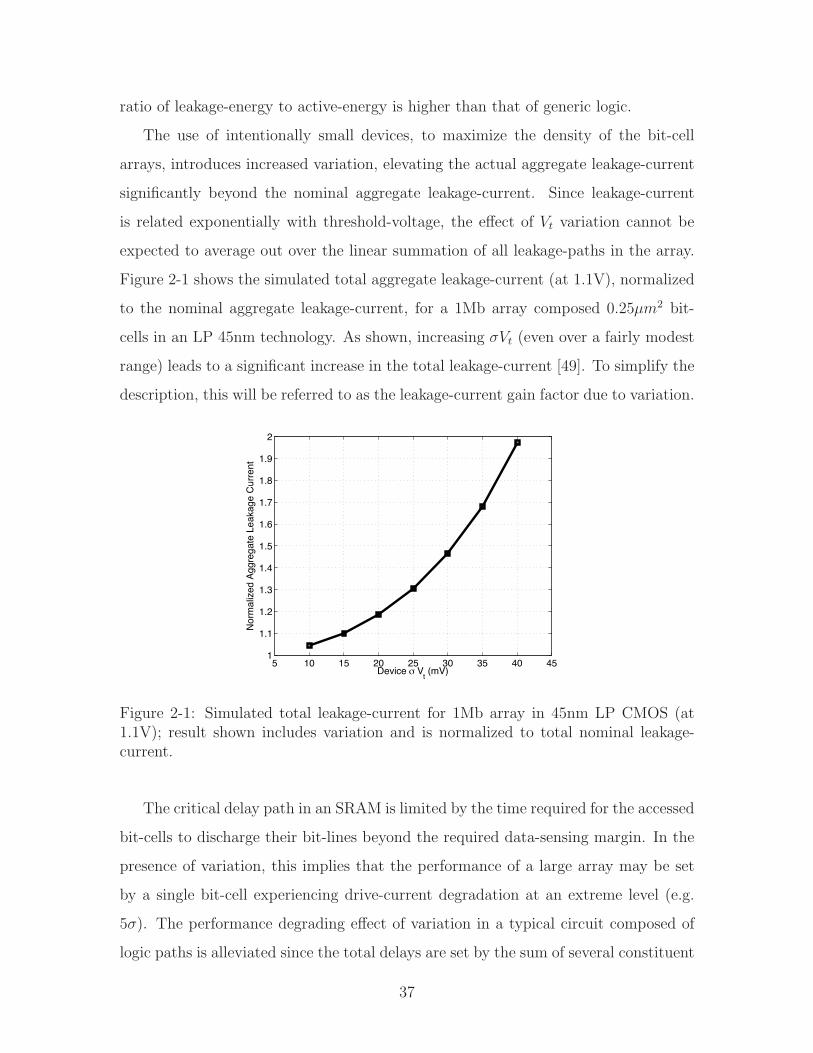
Figure 2-1 shows the simulated total aggregate leakage-current (at 1.1V), normalized
to the nominal aggregate leakage-current, for a 1Mb array composed 0.25µm2 bit-
cells in an LP 45nm technology. As shown, increasing !Vt (even over a fairly modest
range) leads to a significant increase in the total leakage-current [49]. To simplify the
description, this will be referred to as the leakage-current gain factor due to variation.
5 10 15 20 25 30 35 40 451
1.1
1.2
1.3
1.4
1.5
1.6
1.7
1.8
1.9
2
Device σ Vt (mV)
Norm
alize
d Ag
greg
ate
Leak
age
Curre
nt
Figure 2-1: Simulated total leakage-current for 1Mb array in 45nm LP CMOS (at1.1V); result shown includes variation and is normalized to total nominal leakage-current.
The critical delay path in an SRAM is limited by the time required for the accessed
bit-cells to discharge their bit-lines beyond the required data-sensing margin. In the
presence of variation, this implies that the performance of a large array may be set
by a single bit-cell experiencing drive-current degradation at an extreme level (e.g.
5!). The performance degrading e!ect of variation in a typical circuit composed of
logic paths is alleviated since the total delays are set by the sum of several constituent
37
stages [50]. Consequently, extreme variation on any one device has greatly reduced
impact. Unfortunately, in SRAMs the tendency towards large arrays implies the
possibility of extreme variation, and the structure of the read-path precludes the
benefit of delay averaging over many stages. As a result, the overall performance of
an SRAM su!ers far more drastically in the presence of variation.
Considering the active and leakage energy profiles for a general digital circuit [51],
the active-energy scales quadratically in a straight-forward manner as CV 2DD with
respect to supply-voltage. Of course, as a circuit’s VDD is reduced, however, the gate-
drive of the constituent MOSFETs is also reduced, degrading the switching speed.
Consequently, the integration time of the leakage-currents, which is set by the time
required to complete the operation, increases, raising the leakage-energy. The oppos-
ing active and leakage energy profiles are shown in Figure 2-2a for a representative
case (i.e. 32b carry-look-ahead adder in 90nm CMOS).
However, based on the factors discussed above leakage-energy in SRAMs has in-
creased prominence. Specifically, as sketched pictorially in Figure 2-2b, the high ratio
of leakage-paths to actively-switching-nodes and the leakage-current gain factor due
to variation both contribute to raising the leakage-energy curve up-ward relative to
the active-energy curve. Additionally, the severe performance degradation due to the
critical-path’s dependence on a single bit-cell experiencing extreme variation, causes
the leakage-energy curve to shift right-ward, as sketched in Figure 2-2c. This can be
understood by observing that the point at which the leakage-energy begins increas-
ing exponentially occurs at a higher supply-voltage than before; e!ectively, variation
raises the limiting bit-cell’s threshold voltage, and, as a result, supply-voltage reduc-
tion quickly leads to sub-threshold operation, which imposes an exponential increase
in circuit delay.
The result in Figure 2-2c seems to indicate that the optimal VDD for SRAMs
occurs at a relatively high supply-voltage. In fact, however, the energy optimization
picture must be modified by considering the practical power-management approach
discussed in Section 2.1.1. Although the importance of leakage-energy remains high,
it must be considered both during active-access and idle-data-storage modes. As
38
Norm
aliz
edEn
ergy
/Ope
ratio
n
10-4
10-3
10-2
100
10-1
0 0.2 0.4 0.6 0.8 1.0 1.2VDD (V)
Norm
aliz
edEn
ergy
/Ope
ratio
n
10-4
10-3
10-2
100
10-1
0 0.2 0.4 0.6 0.8 1.0 1.2VDD (V)
ELKG
= ! ILKG
VDD
dt
op
EACT
= CVDD
2E
TOT
(a) Energy profiles represntative of genericlogic (90nm 32b carry-lookahead adder).
Norm
aliz
edEn
ergy
/Ope
ratio
n
10-4
10-3
10-2
100
10-1
0 0.2 0.4 0.6 0.8 1.0 1.2VDD (V)
Norm
aliz
edEn
ergy
/Ope
ratio
n
10-4
10-3
10-2
100
10-1
0 0.2 0.4 0.6 0.8 1.0 1.2VDD (V)
ELKG
= ! ILKG
VDD
dt
op
EACT
= CVDD
2
ETOT
Increased relative impact
of leakage current
(b) Relative leakage-energy shift exepcted inSRAMs due to increased ratio of leakage-currentsto active-switching-current.
Norm
aliz
edEn
ergy
/Ope
ratio
n
10-4
10-3
10-2
100
10-1
0 0.2 0.4 0.6 0.8 1.0 1.2VDD (V)
Norm
aliz
edEn
ergy
/Ope
ratio
n
10-4
10-3
10-2
100
10-1
0 0.2 0.4 0.6 0.8 1.0 1.2VDD (V)
ELKG
= ! ILKG
VDD
dt
op
EACT
= CVDD
2
ETOT
Increased
performance degradation
(c) Relative leakage-energy shift expected inSRAMs due to severe performace degradationfrom bit-cell variation.
Figure 2-2: Active- and leakage-energy profiles in digital circuits showing trends ex-pected in SRAMs.
39
discussed below, raising VDD in order to reduce the SRAM access delay has reduced
benefit, as leakage-energy must still be incurred in order to retain data even after the
active-mode.
The following subsections start by describing the operating modes of an SRAM.
Then, the energy components during these modes are identified and analyzed in
detail, especially with respect to the supply- and threshold-voltages. Finally,VDD and
Vt targets are determined to optimize energy.
2.1.1 SRAM Idle-Mode Leakage Reduction
If the SRAM power-supply could be gated after the completion of a required number
of accesses, the picture in Figure 2-2, consisting of one leakage energy component and
one active energy component, could be used to determine the optimal total energy.
However, generally, an SRAM is required to retain its data for an arbitrary length of
time unrelated to its own access-delay. Consequently, the data-retention period can-
not be parameterized by the access-delay, and a new parameter must be introduced to
represent the total length of time data is retained. Specifically, idle data-retention con-
sumes power, and to analyze its energy, the period of the retention-cycle, TCY C,RTN ,
must be considered. Accordingly, TCY C,RTN corresponds to the average duration of
time within which a required number of accesses are to be completed. The required
number of accsses are designed as N . The data stored in the SRAM at the end
of TCY C,RTN must correspond to these accesses, serving as the initial state for the
subsequent set of accesses.
The actual length of time required to complete the N accesses can be set freely
to optimize energy as long as it is less than TCY C,RTN . This time to complete the
accesses is designated as the access-period, TACC . For the remainder of the retention-
cycle (i.e. TCY C,RTN #TACC) only idle-data-storage is required. As discussed in detail
in Section 2.2, the operating metrics associated with idle-data-retention are far less
stringent than those associated with active data reads and writes. As a result, during
idle-data-retention, the power can be much more aggressively reduced. The timing
parameters relevant to SRAM energy are summarized in Figure 2-3.
40
Idle Active (N accesses) idle Active
TCYC,RTN
TACC
Figure 2-3: Summary of parameters relevant to SRAM energy.
A straight-forward and highly e!ective implementation of the low-energy data-
retention mode involves dynamically reducing the voltage across the bit-cell array.
This reduces the leakage-current by alleviating drain induced barrier lowering (DIBL),
an increasingly prominent e!ect in advanced technologies. DIBL pertains to an ef-
fective decrease in the threshold-voltage brought on by increasing the MOSFET VGS;
large VGS induces encroachment of the source/drain depletion regions into the channel
region, reducing the gate to bulk biasing required for channel inversion.
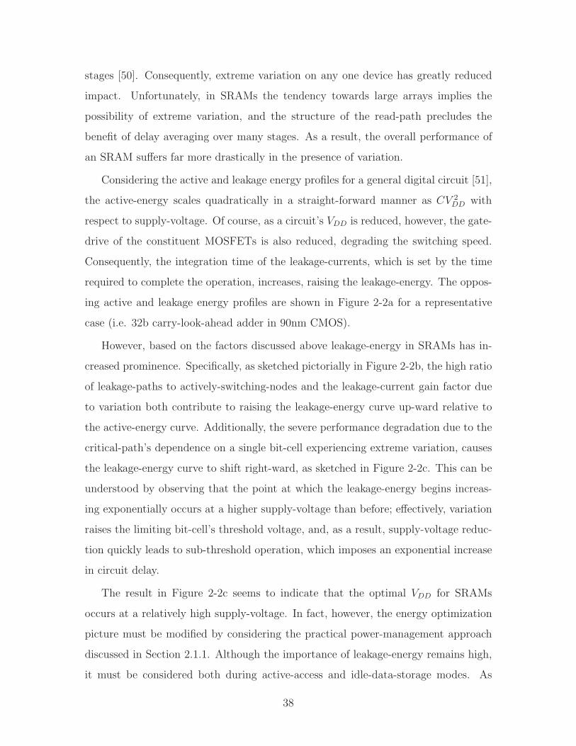
Figure 2-4 shows the normalized leakage-current with respect to supply-voltage
scaling, which also sets the VDS of the devices. Predicite models have been used for
this simulation, and as shown, well over an order of magnitude reduction in leakage-
current can easily be achieved. The leakage-power savings further benefit from the
supply-voltage reduction, leading to over 100x savings with 45nm CMOS when VDD
is scaled from 1.2V to 0.3V.
Practically, this approach has been successful by both reducing VDD [52][53][54][45]
and raising VSS [55][56][57][58][59]. It should be mentioned that an additional ap-
proach involves reverse body-biasing to further reduce the leakage-current [60][61].
Nonetheless, the biasing employed in all of these cases can only be applied to the
point where the data-storage margin is violated. Hence, the data-retention-voltage
(VDRV ) is introduced in [45] to characterize the minimum VDD at which data can re-
liably be retained by the bit-cells. As discussed further in Section 2.2, however, VDRV
is highly subject to variation. Consequently, closed-loop replica techniques have been
employed to estimate the VDRV limit dynamically, so that maximum idle-mode energy
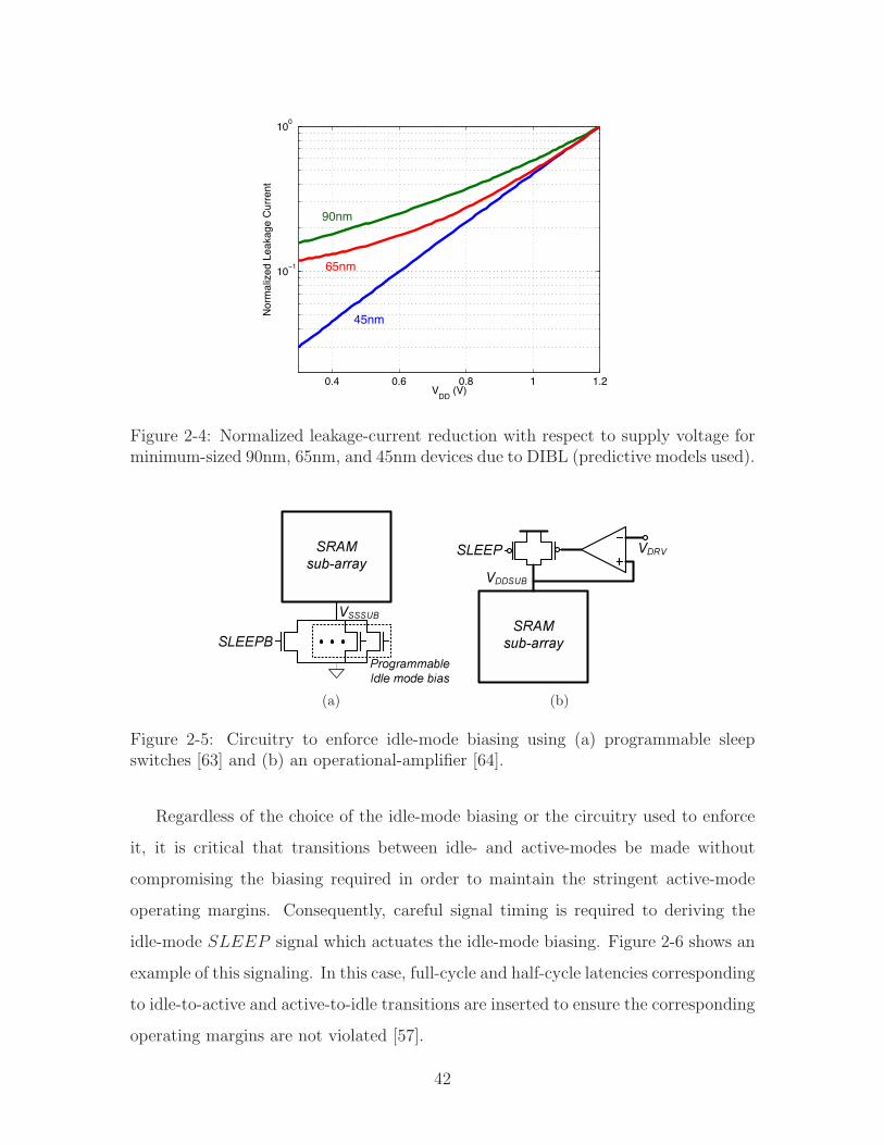
savings can be achieved [62]. In order to enforce a desired VDD or VSS voltage for
the sub-array (i.e. VDDSUB or VSSSUB) during the idle-mode, the supporting circuits
shown in Figure 2-5 have been used [63][64].
41
0.4 0.6 0.8 1 1.2
10−1
100
VDD (V)
Norm
alize
d Le
akag
e Cu
rrent
90nm
65nm
45nm
Figure 2-4: Normalized leakage-current reduction with respect to supply voltage forminimum-sized 90nm, 65nm, and 45nm devices due to DIBL (predictive models used).
SRAM
sub-array
SLEEPB
Programmable
Idle mode bias
VSSSUB
(a)
SRAM
sub-array
VDDSUB
SLEEP VDRV
(b)
Figure 2-5: Circuitry to enforce idle-mode biasing using (a) programmable sleepswitches [63] and (b) an operational-amplifier [64].
Regardless of the choice of the idle-mode biasing or the circuitry used to enforce
it, it is critical that transitions between idle- and active-modes be made without
compromising the biasing required in order to maintain the stringent active-mode
operating margins. Consequently, careful signal timing is required to deriving the
idle-mode SLEEP signal which actuates the idle-mode biasing. Figure 2-6 shows an
example of this signaling. In this case, full-cycle and half-cycle latencies corresponding
to idle-to-active and active-to-idle transitions are inserted to ensure the corresponding
operating margins are not violated [57].
42
Idle Active (N accesses) idle
Clk
SLEEP
VDDSUB
WL
Clk
SLEEP
VDDSUB
WL
Active
Figure 2-6: Waveforms corresponding to idle-to-active and active-to-idle mode tran-sitions.
2.1.2 SRAM Sub-Array Optimal Energy
In this section, the average energy of an SRAM sub-array is considered, and more
specifically, how it can be minimized by judicious selection of supply-voltage, VDD, and
device threshold-voltage, Vt, is analyzed. A typical SRAM is composed of many tiled
sub-arrays, themselves consisting of a bit-cell array and access-control drivers/sensors.
Additionally, global decoding and interfacing circuitry is also required. However, due
to their very specific energy, performance, and operating characteristics (described
above and further in Section 2.2), sub-arrays often employ a separate VDD [65] and
specialized devices [66], where the Vt is engineered for optimal operation. Because
the sub-array critically determines the energy and performance of the entire SRAM,
and because it o!ers independent control of VDD and Vt, this section focuses on how
the sub-array’s energy can be optimized independently of the global decoding and
interfacing circuitry.
Energy Components
Based on the operating model considered in Section 2.1.1, total sub-array energy,
ETOT , has four components, as indicated in Equation 2.1:
ETOT = EACC + ELKG + EIDL + EOH (2.1)
The active-access-energy (EACC) and the leakage-access-energy (ELKG) pertain to the
active mode. EACC corresponds the switching energy required to perform reads and
43
writes, and ELKG corresponds to the leakage-energy imposed by applying a supply-
voltage across the array that must be large enough to ensure reliable reads and writes.
The idle-data-retention energy (EIDL) corresponds to data storage during the idle-
mode, and it will also be referred to as the idle-mode energy. Finally, the overhead-
energy (EOH) corresponds to the overhead incurred due to altering the sub-array’s
biasing in accordance with idle-mode power reduction. These components are sum-
marized in Figure 2-7, and they are described in more detail below.
Idle Active (N accesses) idle
TCYC,RTN
TACC
• EACT
: switching energy for
reads/writes
• ELKG
: Leakage energy to
meet read/write margin
• EIDL
: Leakage energy to meet
hold margin (i.e. at VDRV
)
• EOH
: Overhead energy to
switch between active/
idle-mode biasing
Active
Figure 2-7: Summary of SRAM energy components.
(1) Active-Access-Energy (EACC). This represents the energy required to switch
capacitive nodes in order to generate the control and data signals required to
read and write bit-cells. Signal nodes that transition over the full-range from
VDD to ground require an active access-energy given by CV 2DD, where C is
the node capacitance. Full-swing signals typically include the one-hot enabled
word-line, WL, for row selection, and the one-hot enabled column-select, cSEL,
for multiplexed column selection in a column-interleaved array [67]. Of course,
the internal nodes of the sense-amplifiers also switch from VDD to ground. In
total, the number of sense-amplifiers is equal to the number of columns in the
sub-array divided by the column-multiplexing ratio, m.
The most significant source of active-access-energy consumption, however, is
the bit-lines, BL, which are used to convey the stored read-data to the sense-
amplifiers and to drive new write-data into the bit-cells. However, in some
implementations, the BLs may not discharge completely during data-sensing.
44
Strictly speaking, to resolve the read-data, the BLs need only discharge to the
required sense-amplifier input margin, VSNS, which can be less than 100mV.
Nonetheless, in practice, the BLs are often discharged beyond the sensing-
margin to reduce the probability of data-disruption caused by sustained pulling
of the bit-cell storages nodes towards the BL voltage near VDD. During read-
accesses, for instance, the design in [68] actively amplifies the signal on all BLs
to full logic levels in order to avoid data-disruption. Accordingly, the total
active-access-energy for reads of an i " j (i.e. i-column, j-row) sub-array is
given by Equation 2.2, where the strong dependence on supply-voltage is clear:
EACC,RD = CWLV 2DD + CcSELV 2
DD +i
mCSAV 2
DD + iCBLVDDVSNS (2.2)
Similarly, the total active-access-energy for writes is approximately given by
Equation 2.3:
EACC,WR = CWLV 2DD + CcSELV 2
DD +i
mCBLV 2
DD + im # 1
mCBLVDDVSNS (2.3)
(2) Leakage-Access-Energy (ELKG). This represents the static energy con-
sumed, even in the absence of active-accesses, just to generate a voltage across
the sub-array that ensures the operating margins associated with active-accesses
are reliably met. It comes about as a result of sub-threshold (and other) leakage-
currents through the bit-cell devices that multiply with the supply-voltage,
thereby consuming leakage-power. Since this source leads to static power dis-
sipation, it must be integrated over a time interval to derive its energy. Mini-
mally, the length of time that must be considered is TACC , the period required
to complete some set number of accesses, N . Beyond this, the bit-cell biasing
conditions no longer need to support the active-access operating margins, and
biasing more conducive to minimum power-consumption can be enabled. Ac-
cordingly, the leakage-access-energy for an i" j sub-array is given by Equation
45
2.4, where it is assumed that the entire sub-array is biased with a single VDD
that must meet the active-access operating margins:
ELKG = ij!
TACC
ILKG,BCVDDdt = ijILKG,BCVDDTACC (2.4)
In this expression, the dependence on VDD is explicit through multiplication
with the bit-cell leakage-current, which leads to the leakage-power. However,
the dependence on VDD is also implicit in two other ways: (1) the e!ect of
VDD on ILKG,BC through DIBL, and (2) the e!ect of VDD on TACC through
the VGS available in order to generate bit-cell drive-current needed to discharge
the BLs during data-sensing. Similarly, the dependence on threshold-voltage,
Vt, is also implicit in two ways: (1) the e!ect of Vt on ILKG,BC through the
sub-threshold current equation [69], and (2) the e!ect of Vt on TACC through
the gate-overdrive (i.e. VGS # Vt) necessary to generate bit-cell drive-current.
Additionally, Vt also a!ects the ability of the bit-cells to meet the operating
margins given a particular VDD. Consequently, as described in Section 2.2, Vt
has a direct e!ect on the minimum VDD allowed.
(3) Idle-Data-Retention Energy (EIDL). This represents the static energy re-
quired to retain the data, without any active-accesses, until the end of some
required period. Considering the power-management scenario described in Sec-
tion 2.1.1, system operations will require an average number of accesses, N ,
every TCY C,RTN seconds. The operating point of the sub-array may be chosen
to optimize energy as long as the N accesses are completed in a period less than
TCY C,RTN . For the remainder of the time until the end of TCY C,RTN , however,
the data must be retained so that it is available for the next set of accesses.
This cycle is shown in Figure 2-7. Accordingly, the idle-data-retention energy
is given by Equation 2.5:
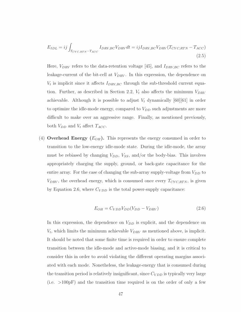
46
EIDL = ij!
TCY C,RTN!TACC
IDRV,BCVDRV dt = ijIDRV,BCVDRV (TCY C,RTN #TACC)
(2.5)
Here, VDRV refers to the data-retention voltage [45], and IDRV,BC refers to the
leakage-current of the bit-cell at VDRV . In this expression, the dependence on
Vt is implicit since it a!ects IDRV,BC through the sub-threshold current equa-
tion. Further, as described in Section 2.2, Vt also a!ects the minimum VDRV
achievable. Although it is possible to adjust Vt dynamically [60][61] in order
to optimize the idle-mode energy, compared to VDD such adjustments are more
di"cult to make over an aggressive range. Finally, as mentioned previously,
both VDD and Vt a!ect TACC .
(4) Overhead Energy (EOH). This represents the energy consumed in order to
transition to the low-energy idle-mode state. During the idle-mode, the array
must be rebiased by changing VDD, VSS, and/or the body-bias. This involves
appropriately charging the supply, ground, or back-gate capacitance for the
entire array. For the case of changing the sub-array supply-voltage from VDD to
VDRV , the overhead energy, which is consumed once every TCY C,RTN , is given
by Equation 2.6, where CV DD is the total power-supply capacitance:
EOH = CV DDVDD(VDD # VDRV ) (2.6)
In this expression, the dependence on VDD is explicit, and the dependence on
Vt, which limits the minimum achievable VDRV as mentioned above, is implicit.
It should be noted that some finite time is required in order to ensure complete
transition between the idle-mode and active-mode biasing, and it is critical to
consider this in order to avoid violating the di!erent operating margins associ-
ated with each mode. Nonetheless, the leakage-energy that is consumed during
the transition period is relatively insignificant, since CV DD is typically very large
(i.e. >100pF) and the transition time required is on the order of only a few
47
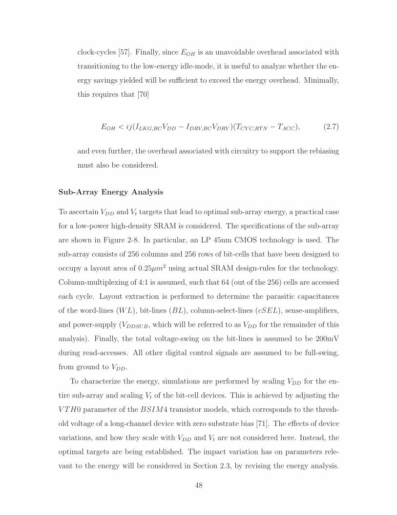
clock-cycles [57]. Finally, since EOH is an unavoidable overhead associated with
transitioning to the low-energy idle-mode, it is useful to analyze whether the en-
ergy savings yielded will be su"cient to exceed the energy overhead. Minimally,
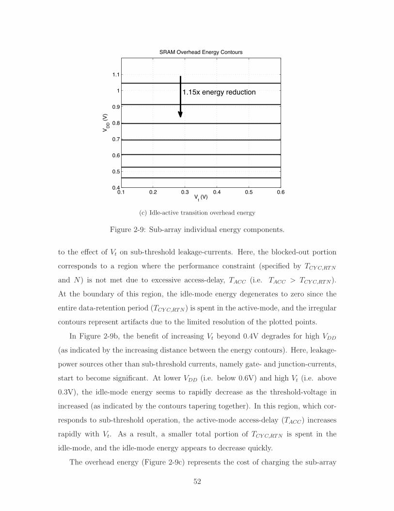
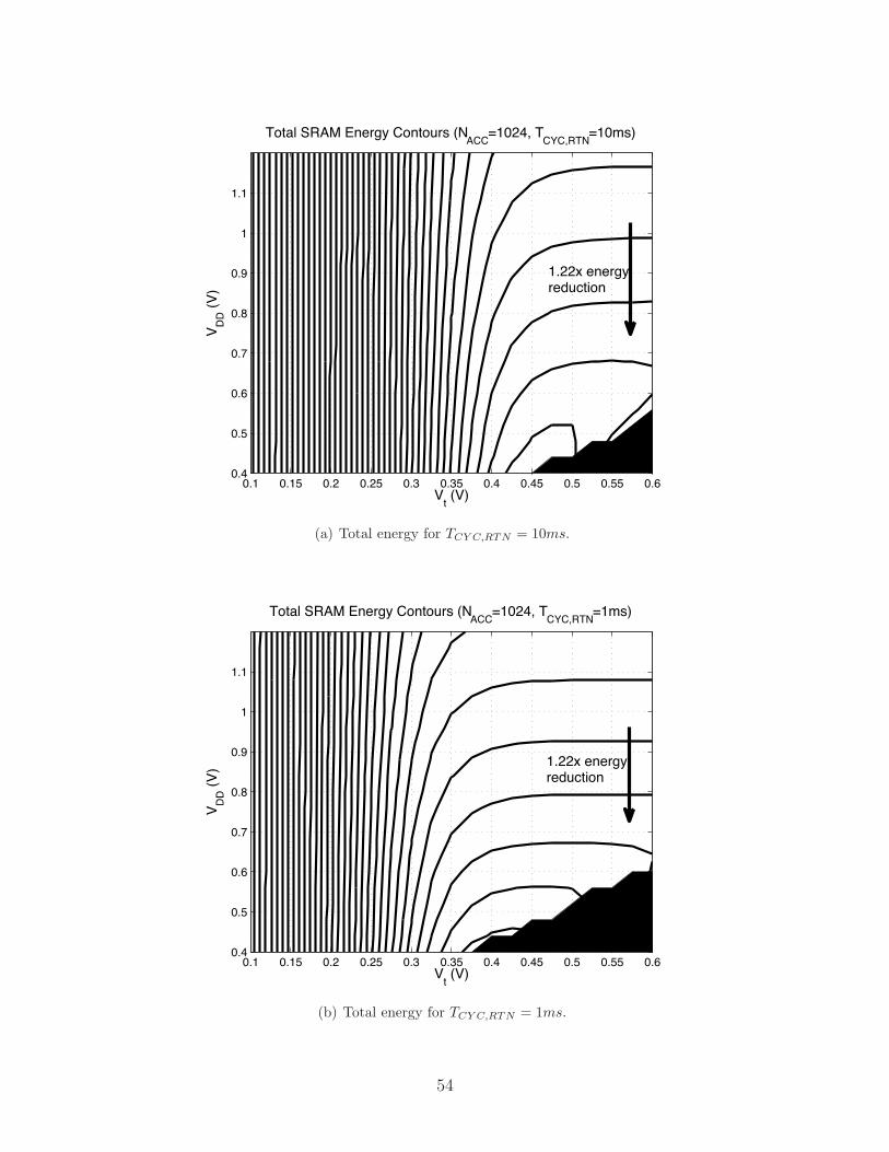
Figure 2-10: Sub-array total energy (at room temperature) for various performancerequirements (specified by TCY C,RTN).
55
sition into the low-power idle-mode. The idle-mode is also beneficial for recovering
additional energy imposed by margining. For instance, some VDD margin is neces-
sary to support changes in the operating conditions and instantaneous peaks in the
performance demands (which require shortening the access-period below the average
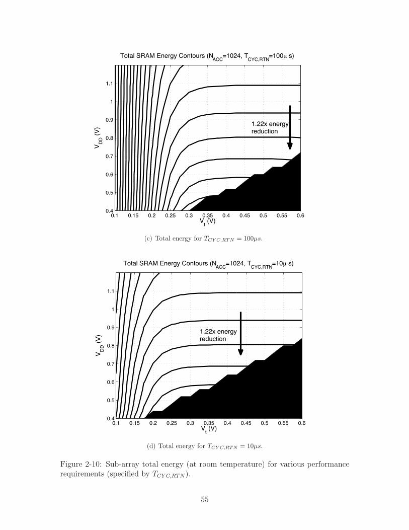
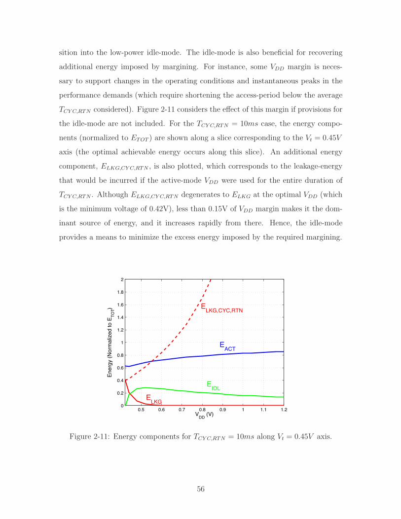
TCY C,RTN considered). Figure 2-11 considers the e!ect of this margin if provisions for
the idle-mode are not included. For the TCY C,RTN = 10ms case, the energy compo-
nents (normalized to ETOT ) are shown along a slice corresponding to the Vt = 0.45V
axis (the optimal achievable energy occurs along this slice). An additional energy
component, ELKG,CY C,RTN , is also plotted, which corresponds to the leakage-energy
that would be incurred if the active-mode VDD were used for the entire duration of
TCY C,RTN . Although ELKG,CY C,RTN degenerates to ELKG at the optimal VDD (which
is the minimum voltage of 0.42V), less than 0.15V of VDD margin makes it the dom-
inant source of energy, and it increases rapidly from there. Hence, the idle-mode
provides a means to minimize the excess energy imposed by the required margining.
0.5 0.6 0.7 0.8 0.9 1 1.1 1.20
0.2
0.4
0.6
0.8
1
1.2
1.4
1.6
1.8
2
VDD (V)
Ener
gy (N
orm
alize
d to
ETO
T)
EIDLELKG
ELKG,CYC,RTN
EACT
Figure 2-11: Energy components for TCY C,RTN = 10ms along Vt = 0.45V axis.
56
2.2 SRAM Operating Margins and Metrics
Aside from the performance constraint specified by TCY C,RTN , SRAMs must meet
several other operating margins that are not considered in the analysis of Section 2.1.2.
The optimal VDD and Vt trends established there are only targets; but enabling actual
sub-array operation at those targets requires overcoming the associated operational
challenges. This section examines how read-margin, write-margin, data-retention,
and read-current depend on VDD and Vt, particularly in the presence of variation.
Generally speaking, the motivation to reduce VDD and raise Vt, based on sub-
array energy optimization, is opposed not only by the ensuing degradation of noise-
margins, but also by an enhanced sensitivity of MOSFETs to variability. Due to
the tendency towards large sub-arrays, the level of variation observed in SRAMs is
extreme, typically beyond the 5! level. Substantial e!ort is devoted to minimizing
SRAM variation. For instance, at the device-level, implant doping (material and
orientation) as well as layout features are carefully controlled [72]. Similarly, at the
array-level, bit-cell redundancy is widely used to mitigate the impact of extreme
variation [73]; nonetheless, in 256"256 sub-arrays, variation beyond the 4! level can
still be expected to limit operation [74].
Figure 2-12 shows the e!ect of variation on MOSFET drain-current (with VGS =
VDS = VDD) in two lights. In Figure 2-12a, an NMOS with Vt = 0.3V is considered as
VDD is scaled for both a mean and 4! device. The distance between the two widens
drastically as supply-voltage is reduced (indicating a degrading ratio of mean-to-4!
current). This comes about due to the increasing dependence of the gate-overdrive,
VDD # Vt, on Vt fluctuations combined with an increasing dependence of the drain-
current on that gate-overdrive (which ranges from linear to exponential towards the
sub-threshold regime [75]).
In Figure 2-12b, an NMOS with VGS=VDS=1V is considered as Vt is scaled.
Threshold-voltages that are engineered to be higher exhibit increased !Vt. This is
due to the need to increase dopant concentration, which leads to more severe random
dopant fluctuation (RDF) [76]. Consequently, to account for the e!ect that Vt scaling
57
has on variation, !Vt has been adjusted using the relationship of Equation 2.8 [77]:
!Vt $"
q2NSUBWDEP
!Vt $#
q(Vt # VFB # 2#F )
COX
!Vt $"
(Vt # VFB # 2#F )
!Vt $"
Vt + 0.1. (2.8)
(Here, #VFB #2#F % 0.1, which has been validated through several data-points from
65nm fabs [77].) As a result, with increasing Vt, the 4! current deviates increas-
ingly from the mean current, particularly as Vt approaches VDD, tending towards an
exponential impact in sub-threshold.
In the following subsections, Monte Carlo simulations are performed on the nom-
inal process conditions, and the statistical device parameters a!ected by variation
(including Vt), are sampled from a Gaussian distribution while considering the im-
pact of VDD and Vt scaling. Here, the e!ect of local-variation (i.e. intra-die) [41],
which most prominently limits SRAM functionality [78], is combined with global
(inter-die) process-skews in order to illustrate the total e!ect.
2.2.1 Read-Margin
The read SNM quantifies the extent to which a 6T bit-cell can reliably hold each of
the two data states required while being subjected to a static read condition. The
read SNM is illustrated graphically in the butterfly plots of Figure 2-13. Here, the
transfer-functions between the bit-cell’s data storage nodes (i.e. from NT -NC and
from NC-NT ) are superimposed. As shown in Figure 2-13a, the static read condition
implies that the access-devices (M5#6) are enabled and the bit-lines are held at VDD.
The cell’s ability to reliably hold both data states depends on the transfer-functions
(plotted in Figure 2-13b) intersecting at two valid logic levels, and it is quantified
by the length of the diagonal of the largest square embedded in the transfer-function
58
0.2 0.3 0.4 0.5 0.6 0.7 0.8 0.9 1
10−6
10−4
10−2
100
VDD (V)
Norm
alize
d I D
4σ
Mean
(a)
0.1 0.2 0.3 0.4 0.5 0.6 0.7 0.8 0.9
10−6
10−4
10−2
100
Vt (V)
Norm
alize
d I D
4σ
Mean
(b)
Figure 2-12: Mean and 4! drain-current for minimum sized NMOS in 45nm CMOSwith respect to (a) VDD (with Vt=0.3V) and (b) Vt (with VDD=1V).
lobes [40].
Figure 2-13b shows how variation can shift the transfer-functions [79], and how
supply-voltage scaling degrades the noise margin, easily leading to the loss of the
read SNM. Similarly, threshold-voltage scaling, has a detrimental e!ect through the
increase in !Vt it introduces.
To determine the combined e!ect of supply- and threshold-voltage scaling, Figure
2-14 shows the mean and variation-a!ected read SNM with respect to VDD and Vt.
For the variation-a!ected case, 4! local variation is considered on top of the process
global-variation. As shown, variation strongly limits the region where read SNM is
59
BLC=VDD
BLT=VDD
M5 M6
NC NT
WL=VDD
(a) Static read condition on bit-cell.
0 0.2 0.4 0.6 0.8 10
0.2
0.4
0.6
0.8
1
NC, NT (V)
NT, N
C (V
)
Read SNM
(b) Read butterfly plot with no variation.
0 0.2 0.4 0.6 0.8 10
0.2
0.4
0.6
0.8
1
NC, NT (V)
NT, N
C (V
)
Read SNM
(c) Read butterfly plot with variation.
Figure 2-13: Read SNM definition through butterfly plots.
60
preserved, specifically restricting operation at low VDD and high Vt, where sub-array
energy tends to be optimized.
0.025
0
0.05
0.05
0.075
0.1 .1
0.1
0
0.1250.125
0.1250.15
0.15
0.150.175
0.175
0.175
0.2
0.2
0.20.2
0.225
0.225 0.225
0.25
0.250.25
0.2750.275
0.3
0.3
0.3250.325
0.35
Vt (V)
V DD (V
)
Mean RSNM (V)
0.1 0.2 0.3 0.4 0.5 0.6 0.7 0.80.3
0.4
0.5
0.6
0.7
0.8
0.9
1
(a)
0
0
0
0.025 0.025
0.0250.05
Vt (V)
V DD (V
)
4σ RSNM with Global Variation (V)
0.1 0.2 0.3 0.4 0.5 0.6 0.7 0.80.3
0.4
0.5
0.6
0.7
0.8
0.9
1
(b)
Figure 2-14: 45nm 0.25µm2 bit-cell read SNM contours for (a) mean case, and (b)4! (on top of global variation) case.
61
2.2.2 Write-Margin
Several metrics exist to quantify write-ability [80][42]. One that relates well to the
read-margin is the ability to make the bit-cell mono-stable at the logic state intended
to be stored [81]. This corresponds to the negative of the read SNM, and is used here.
Figure 2-15 shows the mean and 4! (on top of global variation) write-margin with
respect to VDD and Vt. Once again, variation strongly limits the functional region and
specifically opposes that where sub-array energy is optimized. It should be noted, that
the result shown is for a dense 0.25µm2 bit-cell, which severely constrains the sizing
of the constituent devices. In a practical cell, however, threshold voltage engineering
provides an additional means, beyond just sizing, to set the required relative device
strengths. Here, in order to develop the general trends with minimal complexity,
all Vt’s are assumed to scale equivalently; however, in a practical cell, selective Vt
engineering actually leads to better write-margin. Nonetheless, the increased impact
of variation on write-margin seen at low VDD and high Vt remains, and it critically
contributes to limiting sub-array energy.
2.2.3 Hold-Margin (and Data-Retention-Voltage)
The hold-margin quantifies the ability of the bit-cell to idly retain data in the absence
of read or write conditions. The hold SNM [40] is analogous to the read SNM; however,
as shown in Figure 2-16a, it implies that the bit-cell access-devices are disabled,
precluding the disruption of the storage nodes NT/NC by the bit-lines near VDD.
Consequently, as shown in Figure 2-16b, the hold SNM can be significantly larger
than the read SNM. As shown in Figure 2-16c, this implies the possibility of low VDD
(or high Vt) data-retention even in the presence of variation, leading to much lower
power consumption.
In this manner, the hold-margin is directly related to the data-retention voltage.
Here, the hold SNM is used as the hold-margin, and the VDD where it equals zero
(in the 4! on top of global-variation case) is taken to be the data-retention voltage,
VDRV ; of course, in practice it is prudent to also introduce some additional engineering
62
0
0
0
0.0
0.05
0.05
0.05
0.1
0.1
0.1
0.15
0.15
0.15
0.2
0.2
0.2
0.25
0.25
0.3
0.3
0.35
0.35
0.40.45
Vt (V)
V DD (V
)
Mean WM (V)
0.1 0.2 0.3 0.4 0.5 0.6 0.7 0.80.3
0.4
0.5
0.6
0.7
0.8
0.9
1
(a)
0
0
0.050.10.15
0.2
Vt (V)
V DD (V
)
4σ WM with Global Variation (V)
0.1 0.2 0.3 0.4 0.5 0.6 0.7 0.80.3
0.4
0.5
0.6
0.7
0.8
0.9
1
(b)
Figure 2-15: 45nm 0.25µm2 bit-cell write-margin contours for (a) mean case, and (b)4! (on top of global variation) case.
margin when setting the idle-mode VDD, but the additional margin, which degrades
the power-savings, can be minimized if VDRV can be accurately determined either
through simulation [82][83] or run-time sensing and estimation [62].
63
BLC BLT
M5 M6
NC NT
WL=”0"
(a) Static hold condition on bit-cell.
0 0.2 0.4 0.6 0.8 10
0.2
0.4
0.6
0.8
1
NC, NT (V)
NT, N
C (V
)
Hold SNM
(b) Hold butterfly plot with no variation.
0 0.2 0.4 0.6 0.8 10
0.2
0.4
0.6
0.8
1
NC, NT (V)
NT, N
C (V
)
Hold SNM
(c) Hold butterfly plot with variation.
Figure 2-16: Hold SNM definition through butterfly plots.
64
Figure 2-17 shows the mean and 4! (on top of global-variation) hold SNM with
respect to VDD and Vt. Due to higher dependence on Vt fluctuations and elevated !Vt,
increasing Vt tends to raise the minimum tolerable VDRV . Consequently, the favorable
impact of reducing the leakage-current degrades as Vt is increased. This e!ect is
particularly important at very high threshold-voltages, where the leakage-current is
dominated by gate and junction sources; here, Vt scaling can actually increase the
idle-mode energy due to the higher VDRV required.
2.2.4 Cell Read-Current
The read-current, IRD, is the current sunk by the bit-cell from the bit-line immediately
after its access devices are enabled. The biasing condition implied here is that the
bit-lines are at their precharge voltage, which is typically VDD. The read-current is
a critical metric for sub-array performance, and, as discussed in Section 2.1.2, it also
strongly a!ects the minimum achievable energy.
Figure 2-18 shows the mean and 4! log10(IRD) with respect to VDD and Vt. As
expected, lowering VDD and raising Vt strongly reduces the mean IRD and increases
the further degradation from variation. Improving cell-drive capability is critical
for low-energy sub-arrays not only because this enables more aggressive VDD and Vt
scaling under set performance constraints, but also because it overcomes functionality
failures that are fundamental to SRAMs at the low-energy operating points. These
failures are further discussed in Chapter 3.
2.3 SRAM Energy with Variation
Since VDD and Vt scaling so severely elevates the e!ect of device variation, the optimal
energy analysis of section Section 2.1.2 must be revised. In particular, three impor-
tant e!ects emerge: (1) the access-period, TACC is much longer, (2) the minimum
achievable VDRV is higher, and (3) the total aggregate leakage-current is higher due
to the variation gain factor (illustrated in Figure 2-1). The resulting impact on the
total energy is considered below.
65
0.06
0. 0.12
0.120.18 0.18
0.180.24 0.24
0.240.3
0.30.3
0.36
0.360.36
0.42
0.42 0.42
0.48
0.48 0.48
0.54 0.54
Vt (V)
V DD (V
)
Mean HSNM (V)
0.1 0.2 0.3 0.4 0.5 0.6 0.7 0.80.3
0.4
0.5
0.6
0.7
0.8
0.9
1
(a)
0
0
0
0
0.06
0.06
0.06
0.12
0.12
0.120.18
0.180.18
0.24
0.24
0.24
0.3
0.3
0.30.36
Vt (V)
V DD (V
)
4σ HSNM with Global Variation (V)
0.1 0.2 0.3 0.4 0.5 0.6 0.7 0.80.3
0.4
0.5
0.6
0.7
0.8
0.9
1
(b)
Figure 2-17: 45nm 0.25µm2 bit-cell hold SNM contours for (a) mean case, and (b)4! (on top of global variation) case.
First, regarding the increase in TACC , the most important implication is that the
supply- and threshold-voltage region where the performance constraint is not met
is significantly expanded. Hence, the energy optimization achievable through VDD
66
13
−12
−11
−11
−10
−10
−9
−9
−8
−8
−8
−7
−7
−7
−7
−6
−6
−6
−5
−5
Vt (V)
V DD (V
)
Mean log10(IRD) (log10(A))
0.1 0.2 0.3 0.4 0.5 0.6 0.7 0.80.3
0.4
0.5
0.6
0.7
0.8
0.9
1
(a)
−13−12
−12
−11
−11
−10
−10
−10
−9
−9
−9
−8
−8
−8
−8
−7
−7
−7
−6
−6
−6
−5
−5
Vt (V)
V DD (V
)
log10(4σ IRD) (log10(A))
0.1 0.2 0.3 0.4 0.5 0.6 0.7 0.80.3
0.4
0.5
0.6
0.7
0.8
0.9
1
(b)
Figure 2-18: 45nm 0.25µm2 bit-cell read-current contours (log-magnitude) for (a)mean case (b) 4!.
and Vt scaling is directly limited. As shown in Figure 2-19c-d, this, is particularly
detrimental in the high performance cases (i.e. TCY C,RTN = 100µs, 10µs).
Second, for the low performance cases, the optimal energy is not limited by the per-
formance constraint, TCY C,RTN . For instance for the TCY C,RTN = 10ms case (shown
in Figure 2-19a), the optimal point is VDD = 0.65V and Vt = 0.475V , which oc-
67
Vt (V)
V DD (V
)
Total SRAM Energy Contours (NACC=1024, TCYC,RTN=10ms)
0.1 0.2 0.3 0.4 0.5 0.60.4
0.5
0.6
0.7
0.8
0.9
1
1.1
1.53x energyreduction
(a) Total energy for TCY C,RTN = 10ms.
Vt (V)
V DD (V
)
Total SRAM Energy Contours (NACC=1024, TCYC,RTN=1ms)
0.1 0.2 0.3 0.4 0.5 0.60.4
0.5
0.6
0.7
0.8
0.9
1
1.1
1.53x energyreduction
(b) Total energy for TCY C,RTN = 1ms.
68
Vt (V)
V DD (V
)
Total SRAM Energy Contours (NACC=1024, TCYC,RTN=100µ s)
0.1 0.2 0.3 0.4 0.5 0.60.4
0.5
0.6
0.7
0.8
0.9
1
1.1
1.53x energyreduction
(c) Total energy for TCY C,RTN = 100µs.
Vt (V)
V DD (V
)
Total SRAM Energy Contours (NACC=1024, TCYC,RTN=10µ s)
0.1 0.2 0.3 0.4 0.5 0.60.4
0.5
0.6
0.7
0.8
0.9
1
1.1
1.53x energyreduction
(d) Total energy for TCY C,RTN = 10µs.
Figure 2-19: Sub-array total energy (at room temperature, with variation) for variousperformance requirements (specified by TCY C,RTN).
69
curs well within the region where the performance constraint is met (i.e. TACC is
considerably less than 10ms). The reason for this is that long data-retention periods
require high Vt in order to minimize leakage-power; however, the severe variation that
accompanies this results in extreme performance degradation. The resulting increase
in active-mode leakage-energy (ELKG) cannot be o!set by the leakage-current sav-
ings (which themselves are diminished by the variation gain factor). Consequently,
to reduce ELKG, TACC must be aggressively shortened by raising the supply-voltage.
Of course, the net increase in the leakage-energy, and now also the active-energy, is
extremely detrimental to the absolute total energy (as quantified below).
The e!ect on VDRV also has a strong impact on the total energy, particularly in
the low performance cases where TACC must be reduced far below TCY C,RTN . For
instance, in the TCY C,RTN = 10ms case, the idle-mode power at the optimal Vt (i.e.
0.475V) is higher by over 1.9x compared to the nominal case. This is due to both the
higher VDRV and the leakage-current gain factor from variation.
Overall, the increase in TACC , VDRV , and the aggregate leakage-current has a
severe impact on the absolute total energy. Specifically, for the TCY C,RTN=10ms,
1ms, 100µs, 10µs cases respectively, the increases in the total-energies are 1.65x,
1.56x, 1.28x, and 1.33x compared to the nominal cases. From this analysis the most
important conclusion that can be drawn is that, for ultra-low-energy applications with
modest data-retention periods, it is critical to improve performance in the presence
of variation in order to (1) enable aggressive VDD and Vt scaling, and (2) minimize
TACC so that so that the active-mode leakage-energy can be reduced at a given VDD
and Vt. As the data-retention period becomes extremely long, it also becomes critical
to minimize the idle-mode leakage-power.
2.4 Summary and Conclusions
This chapter investigates the sources of SRAM energy, and, in particular, how they
scale with respect to supply-voltage and threshold voltage. Targets and trends for
optimal VDD and Vt are established. The analysis here is di!erent from that of generic
70
digital logic [44] in two important ways: (1) the general requirement of long-term data-
retention introduces the need for a low-power idle-mode where the power cannot be
assumed to be zero, and (2) due to its extreme impact on SRAMs, variability (and
its dependence on VDD and Vt) must be considered.
With the need to persistently retain data, total SRAM energy optimization, based
on the analysis of a practical sub-array, points to three necessary trends: (1) lower-
ing VDD, despite the prominence of active-mode leakage-energy, far below the value
expected based on generic logic considerations; (2) raising Vt to mitigate leakage-
currents during both active- and idle-modes; and (3) reducing the access-delay to
reduce the active-mode leakage-energy and increase the amount of VDD and Vt scaling
achievable under the performance constraint. Although lowering VDD tends to raise
leakage-energy due to the ensuing increase in the access-delay, the inability to com-
pletely negate leakage-currents following the active-accesses increases its appeal from
the standpoint of active-energy reduction. Nonetheless, analysis of the critical SRAM
operating metrics shows that reliable operation at the low target supply-voltages and
high target threshold-voltages is vehemently opposed by device variability. In par-
ticular, the read-margin (quantified by the read SNM) and the write-margin su!er
the primary operational violations. The hold-margin has other important implica-
tions, particularly with respect to the minimum data-retention voltage achievable,
which degrades as Vt is increased; however, with regards to limiting functionality, the
hold-margin is far superseded by read-margin.
The cell read-current is also critical to the sub-array energy, and su!ers intolerably
at low VDD and high Vt. Specifically, it limits sub-array speed, therefore restricting
VDD and Vt scaling in the presence of a performance constraint. Importantly, how-
ever, because it is so severely degraded by variation at low supply-voltages and high
threshold-voltages, read-current drastically increases the access-delay, elevating the
leakage-energy. Consequently, due to the degradation of read-current, enhancing sub-
array performance is critical. Unfortunately, both read-margin and read-current must
be improved simultaneously, and, as discussed in Chapter 4, design strategies to im-
prove one tend to worsen the other. So, it is beneficial to find some means to improve
71
performance other than targeting read-current (and without increasing VDD or low-
ering Vt), in order to reduce leakage-energy and easily overcome the performance
constraint, thereby facilitating supply- and threshold-voltage scaling.
The following chapters are guided by the energy optimization targets established in
this chapter. Chapter 3 investigates techniques to ensure that the required operating
margins and metrics are met in order to operate SRAMs at low supply-voltages and
high-threshold-voltages. Chapter 4 investigates techniques to improve performance
(while maintaining high density), so that VDD and Vt scaling can be aggressively
employed for maximum energy savings.
72
Chapter 3
Ultra-Low-Voltage SRAM Design
The analysis in Chapter 2 strongly points to voltage scaling in order to minimize the
energy of SRAMs. Achieving reliable functionality at low supply-voltages, however, is
extremely challenging. In fact, in digital systems, SRAMs pose the primary limitation
to low-voltage operation, which is critical for energy-constrained applications. Fig-
ure 3-1 shows the minimum supply-voltage achieved by specifically ultra-low-voltage
designs that have been recently reported [84]. As shown, logic circuits achieve much
better voltage scalability than SRAMs, and the gap is increasing as technology scales.
As highlighted in Chapter 2 the reason for this is two-fold: SRAM noise-margins and
performance are more sensitive to variation than those of logic circuits, and SRAMs
are subject to more extreme levels of variation.
This result suggests that one way to alleviate the low-voltage challenges associated
with SRAMs is to target larger geometry technologies, where the e!ects of variation
and leakage-currents are much less severe. Unfortunately, the critical SRAM metric of
density is equally important, or perhaps even more important, in highly-energy con-
strained systems. There are two important classes of energy-constrained applications
that specifically benefit from technology and/or density scaling:
(1) Dynamic Performance Scalable. Applications such as cellular multimedia
handsets [85] and wireless sensor nodes [25] have relaxed workloads for the vast
majority of the time, but can require bursts of high performance. Dynamic
73
50 100 150 2000
0.1
0.2
0.3
0.4
0.5
0.6
0.7
0.8
Technology Node (nm)
V DD (V
)
SRAMLogic
Figure 3-1: Minimum supply-voltage of specifically ultra-low-voltage designs recentlyreported [84].
voltage scaling and ultra-dynamic voltage scaling [86][87] allows momentary
operation at raised voltages, and advanced technologies a!ord the necessary
speed-ups. An important challenge is managing the trade-o! between low-
voltage functionality and the accompanying overheads to performance and area,
which limit high-voltage high-performance operation [88].
(2) Fixed High-Performance. Applications such as baseband radio processors
[89] and high-resolution video decoders [23] must meet aggressive system through-
put specifications. These leverage extreme parallelism, enabled by area scaling
in advanced technologies, to operate e"ciently at a reduced voltage and fre-
quency [4], which is critical for battery-powered mobile devices.
Despite the challenges and density constraints, the energy optimization analysis
in Chapter 2 suggests that SRAM voltage should be reduced to 0.5-0.6V, or even
lower (i.e. < 0.4V ) if the performance degradations imposed by variation can be
su"ciently overcome. Accordingly, this chapter describes the design and analysis
leading to a 256kb SRAM prototype in LP 65nm CMOS that is intended to operate
below 0.4V and achieves operation down to 0.35V. Operation below 0.4V is essen-
tial, particularly to ensure engineering margin (of 0.1-0.2V) at the target optimal
supply-voltage. Additionally, although the threshold voltage of the implementation
74
technology is fixed, the analysis of Chapter 2 recommends a higher Vt (up to 0.5V),
and a 0.4V demonstration leaves margin for additional device Vt engineering. Fi-
nally, Figure 3-1 illustrates the increasing challenge with technology scaling; hence,
aggressive low-voltage techniques provide some basis for low-voltage SRAMs in future
deeply scaled technologies.
3.1 Low-Voltage SRAM Challenges
Figure 3-2 shows the normalized ID versus VGS behavior of an 65nm LP NMOS
(predictive model) in two di!erent lights. Specifically, two e!ects are shown that are
of critical importance to SRAMs at low-voltages: 1) the severe e!ect of threshold-
voltage variation (shown in Figure 3-2a), and 2) the degradation in the on-to-o! ratio
of the drain-current (shown in Figure 3-2b).
In Figure 3-2a, the on-current initially increases exponentially in sub-threshold,
and then far more slowly in strong-inversion. As mentioned in Chapter 2, threshold
voltage shifts are a prominent result of processing variation and RDF [90][91], and
they essentially cause sideways o!sets. The ±4! case for local-variation, which occurs
commonly in large SRAM arrays, is shown. Although the resulting variability is
relatively small at high voltages, the change in drain-current is severe at ultra low-
voltages (e.g. 0.3V) and can easily exceed three orders of magnitude. This suggests
that relative device strengths cannot reliably be set using conventional techniques
like W/L sizing. As described in Chapter 2, standard high-density SRAM topologies
rely heavily on ratiometric sizing, making them extremely sensitive to this failure
mechanism.
Figure 3-2b plots the ratio of the on-current to the o!-current for the same 65nm
LP NMOS. As shown, the nominal ratio of ION/IOFF degrades from over 105 at
nominal voltages to less than 103 at 0.3V. The impact of this e!ect is even more severe
when the variation picture from above is considered; for instance, with 4! degradation
to ION , the ratio at low-voltages is reduced to less than 102. This implies that there is
now a strong interaction between both the “on” and the “o!” devices when it comes
75
0 0.2 0.4 0.6 0.8 1
10−5
100
VDD (V)
Norm
alize
d I O
N
−4σ
Mean
+4σ
>1000
(a)
0 0.2 0.4 0.6 0.8 1
10−4
10−2
100
VDD (V)
Norm
alize
d I O
N/I OFF
103105
(b)
Figure 3-2: Degradation of LP 65nm NMOS (predicitive model) with respect to VDD
showing (a) drain-current variation and (b) ION/IOFF .
to setting the static voltages of critical nodes. This, once again, is highly problematic
for SRAMs, where high-density requirements call for the integration of many devices
on shared nodes, such as bit-lines.
In the following sub-sections, the basic degradations to MOSFET operation that
are brought on at low-voltages are related more specifically to the design of high-
density SRAMs. First, the precise e!ect on bit-cells is considered, specifically with
respect to the standard 6T topology. Bit-cell modifications that have been used to
address the deficiencies and a!ord some degree of voltage scalability are also discussed.
Then, the challenges related to low-voltage periphery are considered.
76
3.1.1 Low-Voltage Bit-Cell Array
The 6T bit-cell, which is shown in Figure 3-3, fails to operate at ultra low-voltages
because of reduced signal levels and increased sensitivity to threshold-voltage varia-
tion [79]. With this topology, both read and write accesses are ratioed making it very
di"cult to overcome the severe e!ects of variation and manufacturing defects.
M1 M2
M3 M4
M5 M6
NT
BLTBLC
WL
NC
Parasitic
gate-oxide
breakdown
Device
M1-2
M3-4
M5-6
Function
Driver
Load
Access
Figure 3-3: 6T bit-cell for low-voltage analysis.
Read/Write Margin
During read-accesses the cell must remain bi-stable to ensure that either data logic
value that might be stored can be held and read without being upset by transients
that occur at the internal nodes, NC/NT , when the access-devices, M5 # 6, are
enabled. The read SNM is considered in Chapter 2 with respect to VDD and Vt,
and it quantifies the margin against loss of bi-stability by considering the worst-case
condition where the bit-lines (BLT/BLC) remain at the pre-charge voltage of VDD.
It should be noted, that in low-voltage designs, the cell read-current is likely to be
very small (in proportion to the bit-line capacitance), and BLT/BLC do in fact
remain close to the pre-charge voltage for an extended period.
Figure 3-4a shows Monte Carlo simulations of a 65nm LP CMOS bit-cell designed
to fit in a layout area of 0.5µm2 while meeting SRAM design rules for the technology.
As expected from the analysis in Chapter 2, at low-voltages the read SNM is violated.
Similarly, Figure 3-4b shows how the write-margin is lost at low voltages, which
indicates that the cell cannot be made mono-stable [81] at the data state desired to
77
0.2 0.4 0.6 0.8 1−0.1
0
0.1
0.2
0.3
0.4
VDD (V)
Read
/Hol
d SN
M (V
)
Read SNMHold SNM
Mean
3σ4σ
Mean
4σ
3σ
(a)
0.2 0.4 0.6 0.8 1
−0.2
−0.1
0
0.1
0.2
0.3
0.4
0.5
0.6
0.7
VDD (V)
Writ
e M
argi
n (V
) Mean
3σ
4σ
(b)
Figure 3-4: 0.5µm2 6T bit-cell degradation of (a) read/hold SNM and (b) write-margin with respect to VDD.
be written. Finally, the hold SNM (Figure 3-4a) measures the ability of the cell to
remain bi-stable while the access-devices are disabled. As shown, it is preserved to
very low voltages and forms the basis for several bit-cell topologies that modify the
6T structure in order to operate at ultra-low-voltages.
Generally, the read and write failures discussed above arise due to the reduced
signal levels at low voltages and due to threshold-voltage variation, whose impact also
increases at low voltages. The electrical-" ratio [92] is shown in Figure 3-5, and it
is defined as the ratio of the e!ective strength of the driver-devices, M1 # 2, to the
78
access-devices, M5 # 6. As a result, it is a critical metric characterizing the cell’s
immunity against problematic transients on NT/NC during read-accesses. In fact,
it serves to isolate the contribution that variations in the driver and access-devices
have towards read failures. Figure 3-5 shows that the electrical-" ratio, which is
nominally set between 2-3 [93], can degrade by almost four orders of magnitude at
ultra-low-voltages.
M1
M6M5
BLTBLC
WL
M2
0.2 0.4 0.6 0.8 110−6
10−4
10−2
100
102
Elec
trica
l β−R
atio
VDD (V)
Mean,1σ, 2σ, 3σ,4σ
Electrical-! = IDS,M1,2
IDS,M5,6
(VGS,M1,2,5,6 = VDD,
VDS,M1,2,5,6 = VDD)
Figure 3-5: Electrical-" ratio definition and degradation with respect to VDD.
In addition to variation, an equally important e!ect limiting the minimum supply
voltage of a 6T bit-cell is gate-oxide soft-breakdown, resulting in extremely high gate-
leakage from the driver-devices, M1 # 2 [94]. In 65nm and beyond, even with very
high-quality oxide, soft-breakdown unfavorably distorts the read butterfly curves.
This can be envisioned by considering the additional parasitic current path shown
in Figure 3-3, which at low-voltages can be comparable to the PMOS load-device
currents. As a result, this current path lowers the VGS of one of the driver devices,
exacerbating the degradation to the logic ”0” level of NT/NC during read-accesses
[95]. In this manner, soft-oxide breakdown severely limits the minimum voltage where
the read-margin is met.
79
Bit-Line Leakage
In addition to the performance and energy limitations discussed in Chapter 2, the
rapid degradation of cell read-current that accompanies VDD scaling also introduces
critical functionality failures. Specifically, Figure 3-6 shows the worst-case read-data
sensing scenario on one pair of bit-lines. Typically, when a bit-cell is accessed, a droop
can be detected di!erentially on one of the bit-lines, BLT/BLC, with respect to the
other. This requires that the read-current of the accessed-cell discharges the intended
bit-line more rapidly than the aggregate leakage-current, ILKG,BL, which is imposed
on the alternate bit-line. Importantly, however, the aggregate leakage-current on the
alternate bit-line depends on the data stored in all of the involved unaccessed bit-
cells. In the case shown, sense-ability is most severely limited; the stored data in the
unaccessed cells leads to high leakage-current on the alternate bit-line (due to the high
VDS across the associated access-devices), and nearly no leakage-current contribution
to the intended read-current.
“0”
IRD
ILKG,BL
“0”
“0”
“1”
“0”
“0”
Figure 3-6: Bit-line leakage during read-data sensing opposing the ability to detectdi!erential droops.
80
Accordingly, the read-current must be much greater than the worst-case aggregate
leakage-current. As mentioned in Chapter 2, however, VDD and Vt scaling (for optimal
energy) greatly reduces the read-current, especially in the presence of variation. The
severe e!ect due to variation is shown by plotting the weakened-cell read-currents
normalized to the already reduced mean read-current. This is shown in Figure 3-7a
for a 0.5µm2 cell in the target 65nm LP technology. Combining this e!ect with the
ION/IOFF degradation discussed previously, Figure 3-7b plots the worst-case IRD as
a ratio of the worst-case bit-line leakage-current (assuming 256 cells per bit-line). As
shown, at low-voltages, the worst-case IRD is exceeded by the worst-case ILKG,BL,
making data sensing impossible.
The design trade-o!s between electrical-" ratio and the cell read-current suggest
that the symmetric-6T topology imposes inherent restrictions to ultra-low-voltage
operation. The electrical-" ratio can be increased by reducing the strength of the
access-devices; however, this degrades the cell read-current, fatally limiting the ability
to sense read-data. Alternatively, the electrical-" ratio can be increased by up-sizing
the driver-devices (M1# 2). However, the up-sizing required to overcome the degra-
dation shown in Figure 3-5 is too drastic considering the cost on density. Additionally,
a large increase in gate area for the driver-devices can exacerbate the limiting e!ect
of gate-oxide soft-breakdown [95], somewhat opposing the read-margin improvement.
To overcome these limitations, alternate bit-cell topologies have been proposed that
attempt to improve the low-voltage trade-o!s and provide some additional voltage
scalability. These are described below as non-bu!ered-read and bu!ered-read bit-
cells.
Non-Bu!ered-Read Bit-Cells
The key benefit of the 6T bit-cell, compared with other static storage structures, is its
possibility for maximum density. Whether this possibility can be practically realized,
however, is subject to several factors including variability (at the target VDD and Vt),
array configuration, and selective biasing conditions during read/write operations.
As mentioned, the di"culty arises due to the need to simultaneously increase
81
0.2 0.3 0.4 0.5 0.6 0.7 0.8 0.9 110−2
10−1
100
VDD (V)
I RD/m
ean(
I RD)
1σ
2σ
3σ
4σ
(a)
0.2 0.3 0.4 0.5 0.6 0.7 0.8 0.9 110−2
10−1
100
101
102
103
104
105
I RD/I LK
G,B
L
VDD (V)
Mean IRD
3σ4σ
(b)
Figure 3-7: Read-current degradation in the presence of variation (a) with respect toVDD scaling and (b) leading to loss of data sense-ability due to bit-line leakage.
read-margin and read-current while lowering the voltage. For instance, several ap-
proaches exist to overcome variation and enforce the required read-margin; the elec-
trical strength of the access-devices and load-devices can be altered selectively for
read and write operations through precise and adaptive biasing of the word-lines,
82
lending to variation resilient cell layout [96] and global process-skew correction [39].
Unfortunately, however, this degrades the read-current [39] to an intolerable level
at low-voltages. Alternatively, raising the supply voltage for only the bit-cells be-
ing accessed [53] improves the read-margin and read-current but adversely a!ects the
active-access-energy; although the leakage-energy is reduced, the energy saving trends
in Chapter 2 cannot be achieved.
Minimally, the read-margin and read-current trade-o! at low-voltages can be al-
leviated by maximizing the discharge rate of the bit-lines, reducing the disruptive
stress on the bit-cell storage nodes (NT/NC) that tends to raise their voltage. This
is the basis for regenerating the bit-line voltages using a sense-amplifier, as in [68].
Alternatively, the bit-line loading can be aggressively reduced (to less than 16), and
the bit-cell pull-down stack on one side can be aggressively up-sized, leading to the
asymmetric cell shown in Figure 3-8a [97]. Though the read SNM condition is some-
what eased, severe variation at low-voltages makes it di"cult to guarantee that the
read-stress is su"ciently eliminated; further, array area-e"ciency must su!er, arising
from the need to drastically shorten the bit-lines. To completely overcome the read
SNM condition, the 7T cell in Figure 3-8b [98] can be used, where the bit-cell feedback
path is gated by M7 during read-accesses so that the possibility of actively flipping
the stored data-state is eliminated. The additional of M7 leads to an L-shaped lay-
out, leaving gaps for sensing circuitry to be distributed throughout the columns so
that RdBLT can be kept short in order to ensure minimal read access-delay. How-
ever, at ultra-low-voltages, the read access-delay is still quite long. Since NC is held
dynamically, leakage-currents severely compromise data-storage during these periods,
limiting the level of voltage scaling that can reliably be achieved with this bit-cell.
The write operations are somewhat less constrained than read operations, which
depend on both the read-margin (to avoid data-disruption) and the read-current
(to ensure data sense-ability and achieve optimal sub-array energy). The critical
6T SRAM metric associated with write operations is the write-margin, and it is
possible to apply selective biasing to improve the write-margin without simultaneously
degrading any other critical metric. In particular, correct write operation requires
83
M1 M2
M3 M4
M5 M6
RdBLTBLC
WL
M1 M3
M5
M6
BLC
RdBLTVDD
VDD
GND
GND
WrWL
WL
M2M4
WrWL
High read-current
for rapid RdBLT
discharge
(a)
M1
M3
M5
RdBLTBLC
M2
M4
M6
M7
WLB
WrWL
WL
NC
M1 M3
M2M4
M6
BLC
RdBLTVDD
VDD
GND
GND
WLB
M5
M7
Sense Cct 1
Sense Cct 1
Sense Cct 0
Sense Cct 0
(b)
Figure 3-8: Non-bu!ered bit-cells formed by (a) asymmetrically upsizing one pull-down path for rapid RdBLT discharge [97], and (2) addition of device (M7) to gatebit-cell feedback path against disruption [98].
that the NMOS access-devices overpower the PMOS load-devices, in order to store
a new data state. A couple of options exist in order to enhance the strength of the
access-devices relative to the load-devices. First, the bit-lines that are engaged in
the write-operation (recall, column-interleaving implies that only some of the bit-
cells in the accessed row must be written to) can be slightly boosted beyond the
rail-voltages to over-drive the target access-devices [42]. Second, the supply-voltage
84
can be reduced, selectively, for the columns that are engaged in the write-operation,
thereby weakening their PMOS loads [99]. It is important to note here that the
supply-voltage is reduced to all cells in the target columns, including those in the
unaccessed rows; however, since their access-devices are disabled they only face the
hold-condition, which is far less stringent than the read-condition.
Bu!ered-Read Bit-Cells
In order to completely eliminate the possibility of read-data-disruption without in-
troducing additional dynamic nodes (which are highly problematic at low-voltages),
bu!ered-read bit-cells can be used. Here, the bit-cell storage-cell, where data is writ-
ten and held, is explicitly separated from its read-port. This can be done with the
addition of at least two devices, leading to the 8T topology shown in Figure 3-9. The
evolution from a 6T topology is shown, and the additional devices, M7 # 8, form a
read-bu!er which isolates the storage-nodes (M1 # 6) from the read-bit-line, RdBL.
A comparison of the layout for the two cells is also shown, where both adhere to the
“Thin Cell” structure [100], which alleviates lithography stresses and device mismatch
sources by minimizing jogs in the poly. The 6T layout is limited by the pitch of four
devices, while the 8T layout [93] is limited by the pitch of five devices. This layout is
highly e"cient in its sharing of source-drain junctions and poly wires with abutting
cells.
Nonetheless, the additional area overhead introduced, compared with the 6T bit-
cell is unavoidable. Hence, to evaluate the merits of the 8T topology for low-voltage
operation, it must be compared against the approach of up-sizing the devices of a 6T
topology for variation reduction, which would reduced its failure probability due to
read-data-disruption. Further, 6T up-sizing also leads to stronger bit-line pull-down
paths, increasing the cell read-current. Consequently, for comparison, the 8T cell
must use read-bu!er devices (M7 # 8) that are sized equivalently to the 6T driver
and access-devices. Accordingly, in the iso-read-current 8T cell, very little area is left
for the storage-cell (M1 # 6). Importantly, however, the storage-cell must only meet
the hold SNM rather than the far more stringent read SNM, which must be met by
85
M1 M2
M3 M4
M5 M6
BLTBLC
WL
M1 M3
M5 M2M4
M6
BLC
BLTVDD
VDD
GND
GND
WL
WL
NWell
Active
Poly
M1 M2
M3 M4
M5 M6
BLTBLC
WL
M1 M3
M5 M2M4
M6
BLC
BLTVDD
VDD
GND
GND
WL
WL
M6
M7
M8
RdBL
RdWL
M8
M7
RdBL
RdWL
6T bit-cell 8T bit-cell
Figure 3-9: 8T bit-cell and layout (to overcome read-data-disruptions) shown besidesa typical 6T bit-cell and layout.
the 6T bit-cell. Figure 3-10 compares the 4! read SNM of 6T bit-cells and the 4!
hold SNM of the storage-element of 8T bit-cells that have been sized for equivalent
read-current and total layout area (ranging from 0.65µm2 to 1.15µm2) using SRAM
design rules in the target 65nm LP technology. As shown, for each given area, the
8T cell achieves lower voltage operation (by approximately 0.2V), as indicated by the
VDD where the hold/read SNMs equal zero, respectively.
Since it breaks the highly constrained trade-o! between read-margin and read-
current, and because its remaining operating margin (i.e. hold SNM) is much more
robust to variation, the 8T bit-cell is extremely promising for low-voltage operation.
Additionally, for a given layout area, many more options exist to address the low-
voltage challenges. For instance, the read-bu!er’s access-device (M8) can be made
at least as strong as its driver-device (M7), and/or its word-line (RdWL) can be
boosted, both of which lead to greatly enhanced read-current. Additionally, the
threshold-voltages of the storage-devices (M1# 6) can be raised, to manage leakage-
currents (which critically limit the energy savings in both active- and idle-modes), and
the threshold-voltages of the read-bu!er-devices (M7 # 8) can be lowered to further
86
0.1 0.2 0.3 0.4 0.5 0.6 0.7 0.8 0.9−0.2
−0.15
−0.1
−0.05
0
0.05
0.1
0.15
0.2
0.25
0.3
4σ R
ead/
Hold
SNM
(V)
VDD (V)
1.15, 1.05, 0.950.85, 0.75, 0.65 µ m2
8T
1.15, 1.05, 0.950.85, 0.75, 0.65 µ m2
6T
Figure 3-10: 6T bit-cell and 8T bit-cell operating margins for various size layouts(and equivalent read-current) in LP 65nm CMOS.
improve read-current. Finally, with the relaxed operating margin a!orded by the
hold-condition, the storage-element can be aggressively optimized for write-margin.
Although the 8T bit-cell addresses the matter of read-margin very e!ectively, it
still su!ers from bit-line leakage at ultra-low-voltages. To address this, the read-bu!er
has been enhanced in the bit-cells of Figure 3-11 [101][102]. In Figure 3-11a, when
the cell is unaccessed (i.e. RdWL = 0) and NC = 0, NCB is actively pulled-up to
VDD through M10. Hence, sub-threshold leakage from RdBL to NCB is eliminated.
alternatively, when NC = 1, NCB is set by the relative leakage currents from M9
and M10, and PMOS/NMOS threshold-voltage skews in the technology used lead
to higher PMOS leakage currents, once again causing NCB to settle near VDD. In
Figure 3-11b, when the cell is unaccessed, NCB is actively driven to VDD by M10,
regardless of NC. In both bit-cells, however, the read-bu!er enhancement imposes
an additional area overhead of two devices (i.e. 10T cells).
To overcome read-bit-line leakage without additional area overhead, the design
87
M1 M2
M3 M4
M5 M6
BLTBLC
WL
NC
RdWL
M7
RdBL
M8
M9
M10
RdBL
M8
NC=”0"
6T
storage
cell
RdWL=”0"
M9
M10
RdBL
M8
NC=”1"
6T
storage
cell
RdWL=”0"
M9
M10
M7M7
NCB=”1" NCB!”1"
(a)
M1 M2
M3 M4
M5 M6
BLTBLC
WL
NC
RdWL
M7
RdBL
M8
M9
M10
RdBL
NC=”0"
6T
storage
cell
RdWL=”0"
NCB=”1"
M7
M8
M10
M9
RdBL
NC=”1"
6T
storage
cell
RdWL=”0"
NCB=”1"
M7
M8
M10
M9
(b)
Figure 3-11: Bit-cell read-bu!er enhancements to manage bit-line leakage using (a)PMOS/NMOS threshold-voltage skews [101], and (2) active pull-up on internal NCBnode [102].
in [103] uses a standard 8T cell in a general-purpose process with lower threshold-
voltages. This leads to less variation and higher gate-overdrive on the devices (i.e.
improved ION/IOFF ). Consequently, bit-line leakage can be su"ciently managed
by shortening the read-bit-lines (i.e. eight cells per read-bit-line are used). The
degradation to array area-e"ciency is alleviated by using very simple read-bit-line
88
sensing circuitry and maintaining much longer write-bit-lines (BLT/BLC), which
are not susceptible to leakage e!ects (i.e. 512 cells per write-bit-line). Nonetheless,
as discussed in Chapter 2 reducing the threshold-voltage can have a highly detrimental
e!ect on the total energy in low- and medium-performance highly-energy-constrained
applications.
An issue with the 8T bit-cell is that it is not as amenable to a column-interleaved
layout as the 6T bit-cell. During write-operations in a column-interleaved array, only
some cells of the accessed-row are engaged by di!erentially driving write data on to
their bit-lines. The bit-lines of the remaining cells in the row, which are referred to
as half-accessed, are precharged high, imposing a read-condition since their access-
devices are enabled. Truly eliminating the read-condition, then, restricts column-
interleaving, requiring that bit-cells accessed together be layed-out adjacently. Un-
fortunately, soft-errors, caused by radiation of energetic particles [104], exhibit spatial
locality [105], implying that, without column-interleaving, several bits of an accessed
word can be corrupted. In order to avoid the increased complexity of multi-bit er-
ror correction coding (ECC), soft-error immunity can be achieved by using several
ECC bits per row, each corresponding to spatially separated bit-cells. With the 128b
per row configuration of [103], the extra ECC penalty is only 5%. Alternatively, a
bu!ered-read bit-cell has also been proposed to enable column-interleaving; however,
its area overhead is considerable, requiring a total of ten devices (i.e. 10T) [106].
3.1.2 Low-Voltage Periphery
With respect to overall SRAM density, the area of the periphery, including address
decoders, word-line drivers, sense-amplifiers, and read/write data interfaces, is less
important than that of the array. As a result, circuit-styles that are much more
robust to low-voltage operation can be employed. The peripheral decoders and array
control-signal drivers are considered below, followed by the sense-amplifiers
89
Decoders and Drivers
For decoding circuitry and word-line drivers, static CMOS logic gates, free of ratio-
metric functionality dependencies and nominally achieving rail-to-rail signal levels,
are amenable for low-voltage operation [51][107]. This is particularly true if gates
with high input fan-in are avoided, in order to minimize parallel leakage-paths that
degrade the output logic level [108]. Further, in the nominal case, sizing of CMOS
gates for minimum energy also favors high density [109]. In the presence of varia-
tion, however, care in logic gate design is necessary, requiring transistor up-sizing to
ensure that actively “on” pull-up/down networks are not so severely weakened that
that they cannot compete with their complementary pull-down/up networks (which
are nominally “o!”) [110]. Nonetheless, unlike bit-cells, which exhibit extreme lev-
els of variation (i.e. 4-5!) in large arrays, the periphery can be designed for much
less variation, on the order of 3!. Consequently, comparatively modest up-sizing is
required to ensure low-voltage operation.
Sense-Amplifiers
Unlike decoder and driver circuitry, sense-amplifiers have much more stringent oper-
ational requirements than static CMOS logic gates. Even if full-swing bit-line sensing
is used [111], the bit-line logic-levels are severely degraded at low-voltages by two
critical factors: (1) severe bit-line leakage, arising since the paradigm of low nodal
fan-out [108] can not be up-held on the bit-lines, and (2) drastically reduced bit-cell
read-currents, arising since large arrays are subject to to extreme levels of bit-cell
variation.
Of course, by using very short read-bit-lines (e.g. eight), simple CMOS-style
full-swing logic sense-amplifiers can be used [103]. However, in high-density array
configurations, where 256 cells are integrated per bit-line, sense-amplifier inverters
pose one of the primary limitations at low-voltages [81]. To reduce the sensing margin
required, the sense-amplifier inverters’ trip-points can be adjusted by using a replica
column to emulate the logic levels that have been compromised by bit-line leakage.
90
This technique is e!ective in the 130nm design of [102], where the aggregate bit-
line leakage is less than the worst-case read-current, and read-current variation is
su"ciently small to have minimal impact on the bit-line logic-levels.
In advanced technologies, however, low read-current variation cannot be pre-
sumed; further, variation in the sense-amplifiers themselves greatly increases the re-
quired sensing margin. To manage the e!ect of global variation in the sense-amplifiers,
di!erential structures, such as the strong-arm flip-flop (SAFF) [112] or the conven-
tional input-regenerating latch [113], can be used. Di!erential bu!ered-read bit-cells,
such as the 9T design of [114] and the 10T design of [106], provide compatibility at
the cost of density, though pseudo-di!erential sensing can also be employed, as dis-
cussed in Section 3.2.2. Unfortunately, these approaches do not address the critical
concern of local-variation in the sense-amplifiers, which poses a primary limitation to
their own area scaling, and, increasingly, that of the entire array [111].
3.2 Ultra-Low-Voltage SRAM Prototype
In this section the design, implementation, and testing of a low-voltage SRAM pro-
totype is described. Solutions that are practical with respect to the overheads they
introduce are presented to address the challenges discussed in Section 3.1. Impor-
tantly, the design presented is meant to be compatible with technology directions
specifically targeting low-energy and high-density, even though these aggravate vari-
ability. Specifically, a 65nm LP CMOS technology is used. Although the device
threshold-voltages are preferentially optimized for low-power, even higher Vt would
be desirable for the severely energy-constrained applications discussed in Chapter 1.
Consequently, aggressive voltage scaling is pursued in order to leave margin for fur-
ther Vt optimization as well as practical guard-band from supply/ground fluctuations.
The prototype is designed to operate below 0.4V, corresponding to a sub-threshold
supply-voltage. Furthermore, to maximize array area-e"ciency and specifically target
the challenge of bit-line leakage at low-voltages, 256 cells are integrated per bit-line.
Finally, the total capacity of the prototype is 256kb, which can serve as a reasonable
91
size cache for many practical low-energy applications. Accordingly, this design forms
the basis for the SRAM used in actual systems that have been prototyped, including
a low-voltage DSP [11] and H.264 video decoder [23].
3.2.1 8T Bit-Cell with Low-Voltage Circuit Assists
The prototype uses the bit-cell shown in Figure 3-12. It is based on the 8T topology,
employing a 6T storage-cell and a 2T read-bu!er which isolates the storage-cell during
read-accesses. Consequently, as discussed in Section 3.1, the read SNM limitation
is eliminated. The other two prominent limitations, namely bit-line leakage and
write-ability in the presence of variation, are dealt with using the peripheral assists
associated with the BffrFt and V VDD controls, which are described below.
WL
BLTBLC
RdWL
RdBL
M2M1
M4M3
M6M5
M7
M8
VVDD
BffrFt
6T Storage Cell 2T Read
Buffer
Figure 3-12: 8T bit-cell uses two-port topology to eliminate read SNM and peripheralassists, controlling BffrFt and V VDD, to manage bit-line leakage and write errors.
Bit-Line Leakage Assist
The bit-line leakage problem in the single-ended 8T cell is analogous to the problem
in the 6T case (discussed in Section 3.1), except that the leakage-currents from the
unaccessed cells and the read-current from the accessed cell a!ect the same node,
RdBL. Consequently, the parasitic leakage-currents can pull down RdBL regardless
of the accessed cell’s state. Figure 3-13a shows transient simulations where RdBL is
92
correctly pulled low by the accessed cell in the solid curve, but it is also erroneously
pulled low in the dotted curves by the leakage currents of the unaccessed cells. Here,
only the case with 64 cells on RdBL results in any sampling window; of course, the
need for additional engineering margin limits the achievable integration even further.
10 20 30 40
0
0.1
0.2
0.3
0.4
µ s
RDBL
Vol
tage
6T Storage
Cell
“0”
PCHRG
Sub-Vt leakage
“0”
“1” (256 Cells) “1” (128 Cells)
“1” (64 Cells)
(a)
10 20 30 40
0
0.1
0.2
0.3
0.4
µ s
RDBL
Vol
tage
6T Storage
Cell
“0”
PCHRG
“1”
No sub-Vt leakage
“0”
“1” (256, 128, 64 Cells)
(b)
Figure 3-13: Read-bu!er bit-line leakage in (a) conventional case where unaccessedread-bu!er foot is statically connected to ground and (b) this design where unaccessedread-bu!er foot is pulled up to VDD.
In this design, however, the feet of all the unaccessed read-bu!ers are pulled up
to VDD through the BffrFt control, as shown in Figure 3-13b. Consequently, after
RdBL is precharged, the read-bu!er devices have no voltage drop across them, and
they sink no sub-threshold leakage-current. The transient simulation in Figure 3-13b
now shows that RdBL correctly remains high in the dotted curves even when 256
cells are integrated. Some residual droop is still visible; this comes about as a result
of gate-leakage from the read-bu!ers’ access-devices and junction-leakage from their
93
drains. Although some energy overhead is incurred to switch BffrFt, this is roughly
equivalent to WL assertion, and it is much less than the energy of the aggregate BL
switch capacitance.
An important concern with this approach is that the peripheral NMOS device
of the BffrFt driver must sink the read-current from all cells in the accessed row.
As shown in Figure 3-14 (and discussed further in Section 3.2.3), this design has
128 cells per row, making the current requirement of the footer device impractically
large. Unfortunately, this device faces a two-sided constraint, and cannot simply be
up-sized to meet the required drive strength, since this would introduce excessive
leakage-current in the BffrFt driver of the unaccessed rows, and, additionally, the
resulting area increase would o!set the density advantage of using a peripheral assist.
6T 6T
“1”
“1”
6T 6T
“0”
“0”
128 X IREAD
ILEAK
Acce
sse
d
Ro
w
Un
accesse
d
Row
Figure 3-14: BffrFt driver must sink the read-current from all bit-cells in accessedrow, and it draws leakage-current in all unaccessed rows.
Instead, the BffrFt driver is itself driven with the charge-pump circuit shown
in Figure 3-15a. This ensures that, when accessed, the gate-drive of its NMOS is
at least 600mV instead of 350mV, and since this device is in (or very near) sub-
threshold, its current increases exponentially, by over a factor of 500, as shown. As
a result, the devices of the BffrFt driver can be nearly minimum sized, consuming
negligible leakage-power in the unaccessed rows. Additionally, since their gate nodes
have minimal capacitance, the charge-pumps and their boost-capacitors (CBOOST )
can be physically small, occupying just slightly more area than a couple of bit-cells.
94
The charge-pump circuit itself is suitable for this ultra-low-voltage application since
it uses a PMOS, M1, to precharge the boost-capacitor and is free from threshold
voltage drops. The transient simulation in Figure 3-15b shows that when a row
gets accessed, its BFB node gets bootstrapped to nearly 2VDD, and the following
NMOS can easily pull down the feet of the accessed read-bu!ers. A side-benefit of
this approach is that the read-bu!er devices consume no sub-threshold leakage-power
themselves. In a typical 8T bit-cell, the read-bu!er imposes an additional leakage
path. Here, however, that overhead is almost completely mitigated.
0.3 0.4 0.5 0.6100
101
102
103
Norm
alize
d NM
OS
Curre
nt
Input Voltage (V)
>500x
CBOOST
M1M2
M3
VDD
WLB
VDD
Boosted node has minimal capacitance
BFB 128 X IREAD
BffrFt
(a)
0 5 10 15 20 250
0.2
0.4
0.6
Volts
Time (µ s)
WLB
BFB
(b)
Figure 3-15: To resolve read-bu!er footer limitation (a) charge-pump circuit is used(b) BFB node gets bootstrapped to approximately 2VDD increasing the current ofthe BffrFt driver by over 500x.
Write Assist
Write failures occur because, in the presence of variation, it cannot be guaranteed
that the strength of the access-devices (M5#6) is more than the strength of the load
devices (M3 # 4). However, it is possible to enforce the desired relative strengths
95
using circuit assists. For instance, as mentioned in Section 3.1 the appropriate bit-
line voltage can be pulled below ground or, in a non-column-interleaved array, the
word-line voltage can be boosted above VDD in order to increase the gate-drive of
the NMOS access-devices. Unfortunately, both of these approaches require boosting
a large capacitance, either the bit-line or word-line, beyond one of the rails. An
alternate strategy that avoids generation of an explicit bias voltage involves weakening
the PMOS load devices by reducing the cell supply-voltage. Figure 3-16 shows that
as the supply-voltage is reduced, the strength required of the access-devices is eased,
which is reflected by the accompanying decrease in the minimum word-line voltage
that results in a successful write. So, in this design, write-ability down to 0.35V
is ensured by boosting the word-line slightly, by 50mV, but more importantly by
reducing the cell supply voltage to weaken the PMOS load devices.
0.1 0.2 0.3 0.40
0.1
0.2
0.3
0.4
0.5
0.6
Cell Supply (V)
Min
. WL
Volta
ge (V
)
Mean
3σ
4σ
Figure 3-16: Minimum word-line voltage resulting in a successful write with respectto the bit-cell supply voltage.
As shown in Figure 3-17a, all cells in each row share a virtual supply node, labeled
V VDD. Previously, V VDD has been reduced passively by disconnecting its power-
supply [99][101]. However, to ensure write-ability with more aggressive voltage-scaling
in this design, V VDD gets actively pulled low during the first half of the write cycle
by a peripheral supply driver. Despite this, as shown in Figure 3-17b, V VDD does
96
not go all the way to ground because all of the accessed cells contribute to pulling it
back up. Specifically, one of the bit-lines gets pulled low, causing the corresponding
storage node, NT , to go low. Accordingly, the alternate PMOS load device tends
to turn on, introducing a current path from the opposite storage node to V VDD;
in this manner half the bit-cell contributes to pulling V VDD back up through one
of its PMOS load devices and one of its NMOS access devices. Fortunately, this
interaction is quite accurately controllable, since the pull-down devices of the supply
driver are large enough that they experience minimal local variation, and the pull-up
path through all of the accessed bit-cells tends to stabilize variability. It is important
to note, however, that the supply driver does introduce an additional leakage path in
all of the unaccessed rows. To minimize its leakage-current, series NMOS pull-down
devices are used, taking advantage of the stacked-e!ect [115].
Figure 3-10 shows that, by eliminating the read-condition on the storage-element
(M1 # 6), the 8T bit-cell has greatly eased operating margins, allowing it to be
sized much more aggressively. Read-bu!er (i.e. M7 # 8) sizing, however, remains
an important concern due the e!ect of read-current on energy, performance, and
functionality. Importantly, threshold-voltage variation, whose standard-deviation is
inversely related to the square-root of device area, has elevated impact at reduced
voltages (approaching an exponential dependence towards sub-threshold); as a result,
read-bu!er up-sizing has significantly enhanced appeal. Figure 3-18 shows the benefit,
at the 4! level, of upsizing the read-bu!er beyond the dimensions used for a 0.65µm2
cell in the target 65nm LP technology. As shown, even modest increase in the width
and length improves the current gain greatly at low-voltages. The length increase is
particularly beneficial, since, in addition to alleviating variability, it improves even
the mean read-current by e!ectively reducing the device threshold voltages through
the reverse-short-channel e!ect (RSCE); here, increasing length reduces the influence
of high-concentration “halo” doping in the channel region [116]. This e!ect can also
be used to improve the strength of the storage-cell access devices to improve the
write-margin [117].
With regards to the conventional 8T bit-cell layout, length increase by approxi-
mately 40% of the read-bu!er devices can be achieved with nearly no area overhead.
As shown in Figure 3-19, the layout height is limited by two minimum length NMOS
devices (M1, 5 and M2, 6) that require an active-contact between them. However,
since the read-bu!er devices require no contact to their intermediate node, their
lengths can be increased as shown. Additionally, the 8T bit-cell used in this design
requires row-wise control of the BffrFt node. This can be achieved with no addi-
tional overhead, as shown; in this manner, the BffrFt node is shared by two rows,
but the resulting increase in bit-line due to BffrFt activation in the unaccessed cell
is negligible. If V VDD control is not required (i.e. the write-margin is su"ciently
enhanced by storage-cell sizing and device engineering, as suggested in Section 3.1.1),
98
0.2 0.4 0.6 0.8 11
1.5
2
2.5
3
3.5
4
4.5
5
4σ R
ead−
Curre
nt G
ain
(A/A
)
VDD (V)
80% length increase
40% length increase
(a)
0.2 0.4 0.6 0.8 11
1.5
2
2.5
3
4σ R
ead−
Curre
nt G
ain
(A/A
)
VDD (V)
50% width increase
25% width increase
(b)
Figure 3-18: Read-current gain as a result of read-bu!er upsizing (a) via widthincrease, and (b) via length increase (taking advantage of reduced variability andRSCE).
the remainder of the layout can be left unchanged.
In this design, however, V VDD control is required to ensure that the write-margin
does not limit voltage scaling. Further, logic design rules are used (instead of SRAM
rules), leading to a larger bit-cell layout that must be redesigned to minimize area.
The final layout used is shown in Figure 3-20, where all devices have been rotated,
isolating the V VDD node. Additionally, to share V VDD routing/contacts, RdBL rout-
ing/contacts, and PMOS N-wells, the row is physically folded [118], as shown in the
99
M1 M2
M3 M4
M5 M6
BLTBLC
WL
M1 M3
M5 M2M4
M6
BLC
BLTVDD
VDD
GND
GND
WL
WL
M6
RdBL
M8
M7
RdBL
RdWL
BffrFt
M7
M8
BffrFt
No contact
Figure 3-19: 8T bit-cell layout with read-bu!er upsizing and BffrFt control (but noV VDD control).
layout tiling.
BLT
BffrFt
M1
M2
M3
M4
M5
M6
M7
M8
RdBL
WL WL BLC
VVDD
GND
Bit-cell (lower-left)
Bit-cell
(lower-left)
Bit-cell
(lower-right)
Bit-cell
(upper-left)
Bit-cell
(upper-right)
Bit-cell tiling
Figure 3-20: Final 8T bit-cell layout and folded-row tiling.
3.2.2 Sense-Amplifier Redundancy
An important consequence of using a non-column-interleaved layout (described fur-
ther in Section 3.2.3) is that adjacent columns can no longer share a sense-amplifier.
As a result, each column must have its own, making the area of each sense-amplifier
more constrained and increasing the total number in the entire SRAM. This scenario
stresses a general problem observed in deeply scaled technologies. Specifically, the
size of the sense-amplifiers has stopped scaling due to the trade-o! between their sta-
tistical o!set and their physical size [111]. In this design, that trade-o! is managed in
part by using a “full-swing” sensing scheme, where the read-bit-line is allowed to dis-
charge completely. Considering the significant speed-up conventionally obtained by
small-signal sensing, this might seem like a drastic approach. However, as mentioned
in Section 3.2.1 the unaccessed read-bu!ers do impose some minimal droop on their
100
RdBL due to gate and junction leakage. Conversely, as the RdBL voltage level falls,
the unaccessed read-bu!ers start to drive reverse sub-threshold leakage current from
their BffrFt nodes, which are at VDD, on to the RdBL node. The resulting droop
ultimately settles to approximately 120mV. Unfortunately, as mentioned in Section
3.1, read-current variation can cause the read-access time to extend almost arbitrarily,
and, in fact, it approaches the settling time of the transient droop. Consequently, in
this design, a static discipline is adopted that guarantees that the correct data value
can be sensed on the read-bit-line even after the read-current and droop transients
have settled. Specifically, this implies that the o!set of all of the sense-amps must
be bound by the 120mV logic “1” level and ground logic “0” level of RdBL. To
achieve this o!set under the imposed area constraints, sense-amplifier redundancy is
employed, as described in the following sub-sections.
Sense-Amplifier O!set Sources
O!sets in sense-amps come about as a result of global and local-variation in their
devices [41]. Here, global-variation refers to die-to-die variation in devices, and local-
variation refers to mismatch between devices within the same die placed close to each
other. Global-variation can a!ect all of the NMOS devices on the chip di!erently
than the PMOS devices, thereby, for instance, skewing the switching threshold of all
inverters. Alternatively, local-variation can a!ect the switching threshold di!erently
for each inverter.
Importantly, the e!ect of global-variation can be cancelled by using a di!erential
sense-amp, as shown in Figure 3-21. The symmetry in this structure ensures that the
devices in its two branches will not be subject to systematic di!erences in process
variation. Of course, the 8T bit-cell of this design uses a single-ended read-bu!er
and is incompatible with di!erential sensing. Accordingly, pseudo-di!erential sensing
is used, where the actual read-bit-line drives one of the inputs in Figure 3-21, and
an o!-chip reference drives the other high-impedance input. Although this o!-chip
reference provides valuable testability support, for a more integrated solution, the
PMOS input device on the reference side can be separated into two devices that are
101
driven by replica columns providing the worst-case RdBL logic “1” and “0” levels.
Assuming the reference is properly generated, the di!erential signal on the read-bit-
line that must be resolved is 60mV.
RdBLREF
Q
ENB
ENBENB
Figure 3-21: Di!erential sense-amp structure cancels e!ects of global variation.
The remaining source of o!set is local-variation, which is modeled as a random
e!ect whose standard-deviation is inversely related to the square-root of the device
areas [119][120]. This gives rise to the area-o!set trade-o! that is also shown in
the Monte Carlo curves of Figure 3-22. In this design, where there are a total of
1024 sense-amplifiers (as discussed in Section 3.2.3), considerable up-sizing would be
required to keep the number of failures from o!set to an acceptable limit.
Sense-Amplifier Redundancy Concept
As shown in Figure 3-23, sense-amplifier redundancy requires that the read-bit-line
(RdBL) from each column be connected to N di!erent sense-amplifiers. Each of
these has the di!erential structure shown in Figure 3-21, so their o!sets are from
local-variation, and they are therefore non-systematic and uncorrelated. Only one
sense-amplifier from among the N is selected, whose o!set is bound by the high and
low logic levels of RdBL. So, if the selection can be made correctly, only one of the N
sense-amplifiers must have su"ciently low o!set. A similar approach has been applied
to flash ADCs to achieve minimal o!set in the thermometer coded comparators [121].
Importantly, though, the total area for all of the sense-amplifiers is constrained.
So, increasing the amount of redundancy means each of them must be smaller. For
102
0 5 10 150
0.02
0.04
0.06
0.08
0.1
Normalized SA Size
SA O
ffset
(|V|
) Differential Input (60mV)
3σ2σ
1σ
Figure 3-22: Monte Carlo simulations of sense-amp statistical o!set; at expectedinput swing (i.e. 60mV), errors from o!set are prominent.
EN<0> EN<1>
RdBL
Q
REF
EN<N-1>
Figure 3-23: With sense-amplifier redundancy, each RdBL is connected to N di!erentsense-amplifiers.
example, as shown in Figure 3-24a, if N equals 2, each must fit into half the allocated
area, and, if N equals 4, each must fit into a quarter of the allocated area. Unfor-
tunately, reducing the size of the individual sense-amplifiers in this manner increases
the standard-deviation of their o!set distribution, and correspondingly increases their
probability of error. Specifically, the o!set distributions in Figure 3-24b are derived
from Monte Carlo simulations of sense-amplifiers designed to occupy a layout active
area of 40µm2, and the error probability for an individual sense-amplifier, PERR,N , is
defined as the area under its distribution where the magnitude of the o!set exceeds
the input voltage swing expected on RdBL. Here, it is clear that, due to the necessary
103
reduction in its size, the error probability for an individual sense-amp increases as
the amount of redundancy, N , increases. However, the ability to select one structure
with su"ciently small o!set means that the error probability for the entire sensing
network is the joint probability that all of the individual sense-amplifiers yield an
error. The total error probability, PERR,tot, is given by the following:
PERR,tot = (PERR,N)N (3.1)
(N=1) (N=2) (N=4)
Column Pitch
(N=8)
Sense-Amp Area
(a)
−0.1 −0.05 0 0.05 0.1Differential Input Swing (V)
InputSwing
PERR,8
PERR,2
PERR,4
PERR,1
(b)
Figure 3-24: With sense-amplifier redundancy (a) the size of each individual sense-amplifier must decrease, and (b) the individual sense-amplifier error probabilities,defined as the area under the o!set distribution exceeding the magnitude of the inputswing, increases.
The resulting error probabilities for the overall sensing networks are plotted in Figure
3-25 normalized to the error probability of a single, full-sized sense-amplifier. As
shown, increased levels of redundancy result in significantly reduced overall error
probabilities, and at the input swings expected in this design (i.e. >50mV), the
resulting improvement can be well over an order of magnitude. Further analysis of
sense-amplifier redundancy, considering its precise area overheads and how it scales
with increasing device variability (expected in future technologies), is undertaken
below.
104
0 0.01 0.02 0.03 0.04 0.050
0.2
0.4
0.6
0.8
1
Input Voltage Swing (|V|)
Erro
r Pro
b. (N
orm
alize
d to
N=1
)N=2
N=4N=8
Figure 3-25: Increased levels of redundancy significanly reduce the error probabilityin the overall sensing network.
Sense-Amplifier Redundancy Implementation
The actual implementation of redundancy used in this design incorporates two sense-
amps (i.e. N = 2). The analysis above considers a general case of up to N = 8, but at
those levels, the total area must be large enough to accommodate at least 8 minimum
sized structures, and the overhead of the selection logic, which is not considered,
becomes significant (the analysis is revised below to consider this overhead). With
N = 2, the selection logic can be reduced to just two latches and two logic gates.
The rest of the selection circuitry is shown in Figure 3-26. Here, a reference bit-cell
is used with both “0” and “1” read-data values hard-wired. This cell gets accessed
once on power-up, and it enforces the case where the read-bit-line is first pulled low,
and then where it remains high. Fortunately, the logic “1” and “0” levels of the read-
bit-lines are fairly independent of variation between the accessed bit-cells; specifically,
logic “0” is consistently very near ground, and, as mentioned, logic “1” is set by the
aggregate gate, junction, and reverse sub-threshold leakage from all of the read-bu!ers
sharing each read-bit-line. Then, to force the worst-case logic “1” condition, all of the
bit-cells in the array must first be written with data that ensures the gate-voltage of
105
their read-bu!er driver-device (i.e. M7) is zero, minimizing the reverse sub-threshold
current. This can be done in one cycle by simultaneously enabling all word-lines.
Consequently, under a static discipline, the wide distribution in read-current does
not limit the integrity with which the dummy cell emulates each logic level. Then,
the simple state machine in Figure 3-26 determines which of the sense-amps can
correctly resolve each logic level, and only the corresponding structure is enabled. If
both sense-amps work, the first one is selected, and if neither work, the entire SRAM
fails.
2 latch
state
machine
EN0 EN1
Rd
BL
Pe
rip
heral
redunda
ncy
control refRead0
refRead1
saRef
rdncyCtrl
rdncyClk
Ref. Bit-Cell
Figure 3-26: Redundancy selection circuitry consisting of a dummy bit-cell and se-lection state-machine.
Figure 3-27 shows the normalized overall error probability for the sensing-network
with the sense-amp sizes actually used in this design. As shown, at the input swings
of interest (i.e. &60mV), the error probability improves by approximately a factor of
five compared to a single full-sized sense-amp.
106
0 0.02 0.04 0.060
0.2
0.4
0.6
0.8
1
Input Voltage Swing (|V|)
Erro
r Pro
b. (N
orm
alize
d to
N=1
)N=2
Figure 3-27: Overall error probability for implemented sense-amp redundancy schemeimproves by a factor of 5 compared to a single sense-amp scheme.
Redundancy Analysis with Technology Scaling and Overhead
Sense-amplifier redundancy shows promise for easing the area-o!set trade-o!. How-
ever, to evaluate it in a practical scenario, the overhead of the sense-amplifier selection
circuitry must be considered. Furthermore, how the benefit of the technique scales
with technology is also critical, since it is meant to enable sense-amplifier density
scaling at a similar rate as bit-cell density scaling. For this analysis, the case of
N = 2 (i.e. two sense-amplifiers total) will be considered, since this requires minimal
overhead circuitry.
Figure 3-28 shows the overhead selection circuitry required for each sensing-
network (i.e. one per RdBL). Here, a 6T storage-cell is used to store the state
corresponding to the selected sense-amplifier. Then, at power-on, gSET is asserted,
initializing the wrEN flip-flop. This allows simultaneous control across all column
sensing-networks to selectively enable each of the redundant sense-amplifiers so that
all columns can be tested at once using their corresponding hard-wired reference bit-
cell. Additionally, however, the wrEN flip-flops from the columns are connected to
each other to form a shift-register. Subsequently, this shift-register provides individ-
ual and successive assertion of wrEN for each sensing-network so that the desired
107
sense-amplifier can be permanently enabled on a column-by-column basis. The sense-
amplifiers themselves have the structure shown in Figure 3-21, and the input reference,
REF , is set to 0.06V, based on the read-bit-line logic levels expected from simula-
tions. Finally, the sense-amplifier ENB signal is driven by a local NAND gate of
minimum size. Generally, the ENB transition time can have an impact on the sense-
amplifier o!set originating from device geometry mismatch and output capacitance
mismatch [113]. However, at low-voltages the relative impact of these o!set sources
is greatly reduced compared to threshold-voltage mismatch, diminishing the need to
further reduce the ENB transition time.
6T
storage
cell
VVDD
SET
D Q
wrEN
saSEL
saSELB
gSET
shSEL
ENB0
ENB1
gEN
Figure 3-28: Sense-amplifier redundancy overhead circuitry for the case of N = 2.
The sensing-networks for both N = 2 and N = 1, which corresponds to just
one full-sized sense-amplifier with no selection circuitry overhead, are layed-out in
65nm CMOS to occupy a total area (Atot) of 40µm2 each. To consider the impact
of technology, scaling, the dimensions of all devices are reduced by'
2 for 45nm, 2
for 32nm, and 2'
2 for 22nm, and it is assumed that the layout area scales accord-
ingly. For the 32nm and 22nm technology analysis, simulations are performed using a
predictive technology model where it is assumed that the threshold-voltage matching
co-e"cient, AV T0, (i.e. !Vt "'
WL) [122] is the same as that of the 45nm devices.
Though challenging, in reality, e!orts to improve the matching co-e"cient are always
pursued [123][124][125].
108
Figure 3-29 shows the overall error probability for the N = 2 sensing-network
normalized to that of the N = 1 sensing-network. The results are derived from 10k
point Monte Carlo simulations, and curves are plotted until the input voltage swing
exceeds the o!set observed from all samples of the respective N = 1 sensing-networks
(i.e. where their probability of error is too fine for the simulation resolution).
0 0.01 0.02 0.03 0.04 0.05 0.06 0.070
0.1
0.2
0.3
0.4
0.5
0.6
0.7
0.8
0.9
1
Input Voltage Swing (|V|)
Err.
Prob
. (No
rmal
ized
to N
=1)
65nm(Atot =40µ m2)
45nm(Atot =20µ m2)
22nm, predictive(Atot =5µ m2)
32nm, predictive(Atot =10µ m2)
Figure 3-29: Normalized sensing-network (N = 2) error probabilities for di!erenttechnologies and layout areas.
As shown, the selection circuitry overhead, which reduces the active area available
for the sense-amplifiers, degrades the benefit of sense-amplifier redundancy somewhat
(compared to the result in Figure 3-27). Additionally, the normalized improvement
also degrades slightly with respect to technology scaling. Nonetheless, Figure 3-
29 shows that sense-amplifier redundancy provides significant improvement in the
sensing-error probability, well beyond the 45nm node, even as the total sensing-
network area is aggressively scaled from 40µm2 to 5µm2.
109
3.2.3 Test-Chip Architecture
The 256kb SRAM is partitioned into eight bit-cell sub-arrays consisting of 128 columns
and 256 rows (32kb), as shown in Figure 3-30. Each cycle, all 128 bit-cells from a
row are accessed. No additional delay is required when selecting di!erent sub-arrays,
and reads and writes may be performed on consecutive cycles.
8T
8T
8T
8T
PCHRG
[0]
8:1 8:1
[128]
[255]
[0]
Address D
ecoder
SUBA[0:7]
snsREF
x8
RD/WRB
CLK
Figure 3-30: Prototype test-chip architecture, with total capacity of 256kb partitionedin eight sub-arrays.
3.2.4 Measurements and Characterization
The prototype incorporating the 8T bit-cell of Section 3.2.1, the peripheral assists,
and sense-amplifier redundancy, is implemented in an 65nm LP CMOS technology.
A die photograph of the 256kb prototype is shown in Figure 3-31. Measurements are
performed by writing and reading two sets of test patterns: (1) checker-board pattern
110
and its complement over each array, and (2) binary count and its complement down
the rows of the array.
The prototype achieves full read and write functionality down to 0.35V (which is
well below the device threshold voltages), and it retains data down to 0.3V, indicating
that the bit-cell and peripheral assists are successful at enabling a VDD that is close
to the data-retention limit. The following sub-sections describe the characterization
results of the prototype with regards to its leakage power, active performance, and
active power.
1.89mm
1.12
mm
32kb
arr
ay
Addr
dec
oder
Col. periph.
Figure 3-31: Die photo of prototype low-voltage SRAM.
Leakage Power
Figure 3-32 shows the leakage power of the SRAM with respect to supply voltage
for 0"C, 27"C, and 75"C. At the minimum VDD of 0.35V, the total leakage power
is 2.2µW, representing over a factor of 20 in leakage power savings compared to a
supply voltage of 1V. As mentioned, the SRAM also retains data down to 0.3V where
the total leakage power is 1.65µW.
The area and leakage power of this SRAM can be compared to a conventional 6T
design, and the 10T sub-threshold design in [101]. From the actual cell layouts, this
design represents an area overhead of approximately 30% compared to a 6T design
111
0.4 0.6 0.8 110−1
100
101
102
103
VDD (V)
Leak
age
Powe
r (µ
W)
75° C25° C
0° C
2.2µW
Figure 3-32: Prototype SRAM leakage-power; at the minimum VDD of 0.35V, theentire SRAM draws 2.2µW of leakage-power.
and an area savings of approximately 30% compared to the 10T design. Additionally,
the leakage power savings of this design, compared to a conventional 6T design, with
a projected VDD of approximately 700mV [57][126], is over 5x.
Active Performance
Figure 3-33 shows the active read and write performance of the prototype SRAM
with respect to the supply-voltage. As expected, the speed is significantly reduced in
sub-threshold, and at 0.35V, the SRAM operates at 25kHz.
Active Power
Figure 3-34 shows the total (i.e. active plus leakage) power, in the solid curves, and
just the leakage power, in the dotted curves, with respect to the operating frequency.
The leakage power remains a dominant portion of the total power for a wide range
of frequencies, so leakage minimization e!orts are well justified.
112
0.4 0.5 0.6 0.7100
101
102
103
104
Freq
uenc
y (k
Hz)
VDD (V)
25kHz
75° C
25° C 0° C
Figure 3-33: SRAM speed with respect to VDD.
101 102 103100
101
102
Operating Frequency (kHz)
Tota
l and
Lea
kage
Pow
er (µ
W)
75° C
0° C
25° C
Figure 3-34: Total power (solid curves) and leakage power (dotted curves) with respectto operating frequency.
3.3 Summary and Conclusions
The e!ects of voltage-scaling on SRAMs are severe. In particular, standard tech-
niques, especially with respect to the bit-cells (i.e. 6T), fall short for reliable operation
113
at the low voltage (i.e. < 0.5V ) necessary for highly energy-constrained applications.
The severe e!ect of variation intolerably degrades the read and write margins, though
the hold margin is maintained down to the target supply-voltage. Additionally, how-
ever, in the presence of bit-line leakage, read-current degradation a!ects not only
performance, but also the ability to sense read-data on the bit-lines.
SRAMs respond much more poorly to voltage scaling than generic logic circuits
because the solutions specifically prescribed to enable voltage scaling in logic directly
oppose the density and area-e"ciency enhancing techniques employed by SRAMs.
Accordingly, the simultaneous need to improve density and voltage scalability de-
mands specialized approaches for the bit-cells and sense-amplifiers; the address de-
coders and word-line drivers, whose density is less critical and whose operation is
similar to full-swing logic, can leverage the approaches that are e!ective for generic
logic.
With regards to the 6T bit-cell, the trade-o! inherent between read-margin and
read-current implies that the viable means to improve the read-margin is through
device up-sizing in order to manage variation. However, area comparison in the
presence of variation suggests that the 8T topology holds much greater promise for
low-voltage operation. Additionally, it increases the options for write-margin, read-
current, and sensing-margin (i.e. bit-line leakage) optimization by way of sizing,
device-engineering, and selective biasing using peripheral circuit assists. Accordingly,
the described prototype employs an improved 8T bit-cell that relies on low-area-
overhead peripheral assists to achieve complete operation down to 0.35V.
Finally, redundancy, which is heavily relied upon to manage statistical failures at
the 4 or 5! level in typical bit-cell arrays, is valuable in the periphery when statisti-
cal failures, at even the 3! level, become too significant, as they do at low-voltages.
Of course, the benefits of redundancy must be evaluated against the overhead it
introduces. Further, its e!ectiveness must be considered with regards to aggressive
density scaling in advanced technologies where variation has increased severity. Anal-
ysis shows that redundancy of the sense-amplifiers, which are emerging as a critical
limitation to array density scaling, improves their area-o!set trade-o! significantly
114
into the 22nm node, despite the associated area overhead.
115
116
Chapter 4
Performance Enhancement for
High-Density SRAMs
In order to minimize sub-array energy, the analysis in Chapter 2 points to the need
to enhance SRAM performance without raising the supply-voltage or reducing the
threshold-voltage. Specifically, a reduced active access-period, TACC , implicitly low-
ers the leakage-access-energy or, even more significantly, allows further supply- and
threshold-voltage reduction, which optimizes the energy for a given performance con-
straint. Although a variety of techniques, including parallelism and pipelining [4], ex-
ist in order to improve the performance of general logic (and promote voltage scaling),
SRAM design is highly constrained by its structure and need to maximize density,
hence requiring very di!erent approaches. For instance, in high-density, low-power
sub-arrays, bit-line discharge (by the accessed bit-cells) poses the critical limitation
to access-time, and unlike with multi-stage or parallel data-paths, it cannot be de-
composed physically or logically to reduce the overall delay. Further, as described in
detail in this chapter, density and noise margin constraints in 6T bit-cells severely
limit the options for addressing this critical delay. 8T bit-cells (or other asymmetric
topologies) alleviate these limitations greatly, but they increase the complexity of
bit-line sensing. Of course, the sense-amplifier itself plays a key role in determining
the overall access-time as well, and for both these reasons, it can greatly impact the
performance achievable by the sub-array at a given supply- and threshold-voltage.
117
Importantly, however, sense-amplifiers face their own density-o!set trade-o!s, which
have increased severity in advanced technologies to the point of posing a primary
challenge within high-density sub-arrays. Accordingly, this chapter investigates a
sensing approach to address sub-array performance while maintaining bit-cell and
sense-amplifier density.
Since energy remains the paramount concern, the analysis is undertaken with
consideration to low-power technology optimizations. The target technology used
to demonstrate the proposed techniques is 45nm LP CMOS, which highlights the
variability associated with density maximization. Additionally, the sensing approach
is applied to 0.25µm2 6T bit-cells, which are the densest achievable in the target
technology and further emphasize noise margin and read-current limitations. Since
8T (and other asymmetric) bit-cells hold increasing promise for low-energy SRAMs,
the issues associated with single-ended sensing are specifically considered.
The following sections start by identifying the challenges associated with both
bit-cells and sense-amplifiers that limit SRAM performance. Then, the advantages of
single-ended sensing, both for alleviating the performance limitations and enabling ag-
gressive voltage scaling, are investigated. Finally, the prototype testchip is presented
that demonstrates a single-ended sense-amplifier to address the critical performance
limitations.
4.1 High-Density SRAM Performance Challenges
Both the bit-cell array and the bit-line sense-amplifiers are critical factors in deter-
mining the overall performance of the SRAM sub-array. This section describes the
basic trade-o!s and challenges inherent in both of these in high-density designs.
4.1.1 Bit-Cell Read-Current
The most urgent performance challenges in bit-cells arise from extreme variation. In
the 6T topology this raises an inherent trade-o! between read SNM and read-current,
severely limiting the sub-array performance improvement achievable by way of bit-cell
118
design alone. As mentioned, the 8T bit-cell (and several other asymmetric topologies)
overcome this trade-o!, leading to significant overall performance improvement (as
discussed in Chapter 3).
IRD/CBL Degradation
Low-power SRAMs must incur the reduced read-current that comes with technology
optimizations to manage leakage-currents, such as raising Vt. Figure 4-1a shows
how the read-current of a 6T bit-cell scales further with cell size. The reduction in
mean read-current is a direct consequence of reducing the size of the driver devices.
However, the increased variation in the smaller devices also results in more severe
degradation to the weak-cell read-current in proportion to this already reduced mean
read-current. For instance, at the nominal voltage of 1.1V, the 5! read-current for the
6T 0.25µm2 cell is easily degraded by an additional factor of two, and, as mentioned
in Chapter 3, the degradation is even more severe as supply-voltage is reduced.
0.2 0.25 0.3 0.35 0.4 0.45 0.50
0.2
0.4
0.6
0.8
1
Norm
alize
d Re
ad C
urre
nt (A
/A)
Cell Area (µ m2)
5σ
Mean
(a)
MC
MC
MC
“1”
“0”
“0”
IRD
Up
to
2
56 ce
lls p
er co
lum
n fo
r
ma
x. de
nsity
(b)
Figure 4-1: Degradation in bit-line discharge time for high-density SRAMs caused by(a) reduced cell read-current and (b) increased bit-line capacitance.
Furthermore, in high-density arrays, the integration of many cells per bit-line
(up to 256) in order to maximize array area-e"ciency, leads to very large bit-line
capacitance. As shown in Figure 4-1b, the resulting ratio of IRDCBL
, which is critical to
the array’s performance, su!ers even further.
119
6T Read SNM Degradation
In 6T cells, increased variation in the highest density bit-cells degrades the read SNM
in the same manner as the read-current [79]. Figure 4-2a shows this reduction (at the
5! level) as the cell area is scaled. Once again, this result is at the nominal voltage of
1.1V, but the impact is even more severe with supply-voltage scaling. Thus, in high-
density 6T bit-cells, read-current and read SNM, which are both critical metrics, are
simultaneously stressed. Exacerbating the matter even further, these metrics exhibit
a strong inverse correlation, as shown in Figure 4-2b [127]. As mentioned briefly in
Chapter 3, this comes about as a result of the bit-cell access-devices, which must be
strong for maximum read-current but weak for maximum read SNM. Unfortunately,
then, optimizations targeting one are likely to worsen the other. Nonetheless, for
functionality, read SNM remains the paramount concern, and cell design trends and
circuit assists preferentially aim to improve it, leading to further reduction in read-
current [39].
0.2 0.25 0.3 0.35 0.4 0.45 0.50
0.2
0.4
0.6
0.8
1
Norm
alize
d Re
ad S
NM (V
/V)
Cell Area (µ m2)
5σ
Mean
(a)
0 0.5 1 1.5 2
0.5
0.6
0.7
0.8
0.9
1
1.1
1.2
1.3
1.4
1.5
No
rm
alize
d R
ea
d C
urre
nt (A
/A
)
Normalized Read SNM (V/V)
(b)
Figure 4-2: Read SNM trade-o! in high-density SRAMs limited by (a) cell size and(b) inverse correlation with cell read-current, caused by opposing access-device re-quirements.
Density and stability trade-o!s imply the urgent need for an alternate method
to recover the ensuing loss in array performance. As mentioned in Section 4.2, 8T
bit-cells (which overcome this interdependence), impose the additional need for single-
120
ended sensing.
4.1.2 Sense-Amplifier Delay and Uncertainty
The total read access-time depends on both the bit-line discharge delay and the
sense-amplifier delay. This section considers the factors a!ecting the sense-amplifier
delay and those related to the sense-amplifier o!set; o!set sets the required bit-
line discharge, thereby strongly a!ecting the overall delay. Further, just like o!set
is managed by increasing the timing margin, strobing timing variation introduces
timing uncertainty, raising the need for additional timing margin and further limiting
the overall delay.
Sense-Amplifier Delay
Two commonly used strobed sense-amplifiers are shown in Figure 4-3. The delay
of these structures, after assertion of the STRB signal (whose own impact is con-
sidered in detail below) can be separated into two phases [128]: 1) development of
output di!erential, and 2) regeneration of output. Though output di!erential begins
developing (somewhat regeneratively through the NMOS devices) immediately after
STRB assertion, full regeneration is defined to begin after the PMOS loads turn-on,
actively pulling-up one of the output nodes.
STRB
RSTBRSTB
IN/OUTINB/OUTB
M1 M2
M3
(a)
STRB
RSTBRSTB
OUTBOUT
IN INB
M1 M2
M3
(b)
Figure 4-3: Conventional strobed sense-amplifier topologies with (a) one input-outputport and (b) separate input-output ports.
Output di!erential (which is also the input di!erential in the case of the first
121
sense-amplifier) is developed through the NMOS pull-down devices (M1 # 3). As a
result, it depends on the initial input di!erential and the NMOS transconductances.
Of course, the initial input di!erential, after full assertion of the word-line, depends
on the bit-cell read-current and the bit-line capacitance. On the other hand, the
delay to regenerate the outputs to restored logic levels depends primarily on the
initial output di!erential, which is amplified at an exponential rate. Consequently, a
large inital output di!erential reduces the delay of the rail-to-rail output regeneration
phase. However, as expected, techniques to generate a large output di!erential can
considerably extend the first phase, and, as a result, the overall optimal conditions
are highly dependant on implementation parameters, including the rate of bit-line
discharge and the sense-amplifier structure used.
For instance, reducing the input common-mode voltage, VIN,CM , reduces the
strength of both NMOS pull-down paths, leading to increased time for output di!er-
ential development; however, the proportional reduction in strength of the pull-down
path associated with the drooping bit-line is increased, resulting in larger output
di!erential at the start of the second phase. Hence, rail-to-rail regeneration occurs
more quickly. Accordingly, in [128], the optimal delay for the sense-amplifier consid-
ered is achieved with an initial bit-line precharge voltage at approximately 80% of
VDD. It is important to note, however, that although slightly reducing the bit-line
precharge voltage can improve the read SNM, it degrades the bit-cell read-current
(with increasing impact in advanced technologies).
Reducing the transition rate of the STRB signal has a similar e!ect to reducing
the bit-line precharge voltage. It, once again, reduces the strength of both NMOS
pull-down paths, increasing the delay of the first phase (i.e. output di!erential de-
velopment) but also resulting in a larger output di!erential at the end of this first
phase. In [113], the optimal delay for the entire access-time is achieved by slowing
the STRB edge delay to over twice its minimum transition time.
122
Sense-Amplifier O!set
Sense-amplifier o!set leads to an increase in the bit-line droop required in order to en-
sure correct data read-ability, extending the read access-time. The trade-o! between
device up-sizing and o!set is well known, both with regards to area, which a!ects
Vt variation [119][120], and linear length and width, which a!ects geometry variation
[122]. This trade-o! is the primarily limitation to sense-amplifier area scaling, which
is emerging as a dominating limitation in high-density sub-arrays [111].
The bias conditions of the sense-amplifier devices also strongly impact its overall
o!set in the presence of variation. For instance, during the first phase (i.e. output
di!erential development), lowering the gate overdrive (VGS # Vt) of the input devices
(M1 # 2) reduces the relative impact of geometric and load-capacitance imbalance
between the two sense-amplifier branches compared to the intended input voltage
imbalance. As a result, o!sets due to geometry and capacitance variation lead to
reduced input o!set [129][130]. This serves as motivation to minimize the edge rate
of the STRB signal, which is shown to reduce o!set by over 40% [113]; and it serves
as motivation to reduce the bit-line precharge voltage, which improves the sensing
yield by over 30% (for a 60% reduction in the precharge voltage) [128].
In addition to sense-amplifier o!set mitigation through device sizing and bias-
ing, various forms of active o!set cancellation have also been investigated. For in-
stance, the DRAM designs in [131] and [131] actively bias the bit-lines to compen-
sate the sense-amplifier’s input o!set. Since the bit-line capacitance is quite large,
these schemes can lead to long o!set-compensation phases and high power consump-
tion. Alternatively, the o!set can be compensated by triming the discharge rate of of
the sense-amplifier’s di!erential branches; using switchable current-sources and load-
capacitors, this can be accomplished with a highly digital scheme [132][133], though
an explicit calibration phase and control circuitry is necessary.
123
Sense-Amplifier Strobing Uncertainty
The sense-amplifier strobe signal must ensure that enough time is allocated for bit-
line discharge to overcome the sense-amplifier o!set. However, as shown in Figure
4-4a, the bit-line discharge time depends on the delay through the array read-path,
which is limited by the weakest bit-cell. Such a cell, whose statistical characteristics
might be beyond the 5! level, is impossible to replicate in the strobe control path.
Consequently, as shown in Figure 4-4b, the timing of the two paths diverges greatly
over process, voltage, and temperature corners [134], even if carefully laid-out SRAM
devices are employed in the strobe path, as in [135].
For this simulation, the read-path is designed to overcome a sense-amplifier o!set
of 50mV, and an array configuration of 256 " 256 is considered; however, the strobe
path must be designed such that it is longer than the array read-path in all cases.
As shown in Figure 4-4b, this implies that in many cases it will be much longer
than it needs to be, thereby excessively limiting the overall performance. In fact, the
overall worst-case delay need only be 820ps based on the read-path delay; however,
the actual worst-case delay is 980ps, limited by the strobe-path, imposing an excess
overhead of nearly 20%. To recover this, designs such as [134] have gone as far as
using temperature sensors to adjust the relative read-path and strobe-path delays, and
automatic compensation based on process and voltage can be even more challenging.
4.2 Single-Ended Sensing
With regards to the bit-cell, one way to address the severe read SNM limitation and
independently improve the read-current is to use an alternate structure. Asymmet-
ric cells, including 6T [97], 7T [127], and 8T [93] topologies, can have much wider
operating margins and significantly increased read-current, making them particularly
compelling in the face of increasing variation [103][13][136]. However, none of these
provides a di!erential read-port, and, therefore, they require a compatible means for
e"cient single-ended sensing.
The most common technique used with single-ended-read bit-cells is full-swing
124
MC
MC
MC
MC
WLE
STRB
Array
read path
Strobe path
5-sigma
bit-cell
(a)
0 10 20 30 400
0.2
0.4
0.6
0.8
1
PVT Corner
Dela
y (n
s)
Strobe PathArray Path
Worst−casestrobe delay (980ps)
Worst−case array delay (820ps)
Equaldelays
(b)
Figure 4-4: Array read-path and sense-amplifier strobe-path (a) limited by match-ing to 5! bit-cell and (b) exhibiting severe delay divergence over process-voltage-temperature conditions, leading to excess overall delay.
sensing [111]. Here, the read bit-line must discharge almost completely so that the
read data can be detected by a sensing structure that may be reduced to essentially
a logic gate. This, however, leads to excess active-switching energy, and, in order
to maintain performance, bit-line discharge times must be reduced by enhancing
the read-current and minimizing the bit-line capacitance. Since altering supply- and
threshold-voltages impacts the energy, this implies the need for large bit-cells and very
125
short bit-lines. Unfortunately, both of these directions severely degrade the density.
Alternatively, small-signal sensing can be retained by employing a pseudo-di!erential
sense-amplifier, as in [137]. However, the need to generate a complementary reference
is unavoidable, and, importantly, it must track all operating conditions even with re-
spect to cells in the tails of the arrays statistical distribution. As a result, design and
testability of the complementary reference is highly complicated.
Noise Sensitivity
An important draw-back to any single-ended sensing scheme is the loss of common-
mode noise rejection capability on the power-supplies, bit-lines, and substrate. Since
no distinction can be made between noise on the bit-line and read-data droop, it
becomes critical to ensure a desired level of bit-line noise-margin. Consequently,
an inherent trade-o! is introduced between sense-amplifier input sensitivity, which
ultimately a!ects the sub-array’s performance, and its robustness to noise. For power-
supply and substrate noise, though there is no inherent trade-o! between sensitivity
and noise-rejection, it is critical to characterize the sense-amplifier’s noise margins.
This can be extremely challenging since, in general, phase and frequency content of
the transient noise can change its impact on the sense-amplifier as they do for bit-cells
[138].
4.3 High-Density SRAM Prototype
In this section, a sense-amplifier designed to maximize the performance of high-density
low-power arrays is presented. It is prototyped in an 45nm LP CMOS process and
integrated with a 64kb array composed of 0.25µm2 bit-cells. The high-density bit-
cells and low-power technology optimizations stress read-current limitations, and the
array configuration (256 " 256) stresses read-bit-line capacitance, which all lead to
long discharge times.
126
4.3.1 Non-Strobed Regenerative Sense-Amplifier
The non-strobed regenerative sense amplifier (NSR-SA) shown in Figure 4-5 ad-
dresses the limitations described in Section 4.1. Two cascaded inverters (M1 # 2
and M3 # M4) form an amplification path that is self-biased for high-gain by the
feedback switches, SAZ . As described below, these also perform o!set-compensation
of the inverter amplifiers via input auto-zeroing [139]. Importantly, to support small-
signal sensing, which greatly improves the density, performance, and power trade-o!s
of the array, the large gain required is achieved most e"ciently through regeneration
[140]. Accordingly, the regenerative device, M5, provides very large positive-feedback
gain. A critical feature is that regeneration requires no external enable or strobe sig-
nal, thereby overcoming the severe tracking uncertainty described in Section 4.1.2.
Instead, the ideal DC transfer function, shown in Figure 4-5, is implemented in contin-
uous time, and the precise point at which regeneration is enabled depends only on the
input bit-line voltage (with respect to the internal reference, VTRIP ). Further, VTRIP
is very stable despite variation since it is generated implicitly by the original auto-
zeroing, and, additionally, its precise value can be selected by design. Accordingly,
this sense-amplifier, which is single-ended and compatible with asymmetric bit-cells,
can enforce a desired balance between sensitivity and noise-rejection.
RSTB
QB
RSTB
Regenerative
feedback
device
Inverter amplifiers
IN
M1
M2
M3
M4
M5
M6
SAZ
SAZ
SREG
SREG
QB
VDD-IN
VTRIP
Infinite gain
at VTRIP
Figure 4-5: Non-strobed regenerative sense-amplifier (NSR-SA) schematic and idealtransfer function.
127
Basic Operation
The NSR-SA operates over two phases: reset and detection. The reset phase occurs
during SRAM bit-line pre-charge, where the sense-amplifier does not need to detect
bit-line droop. Hence, this time is used to perform self-correction of o!sets via auto-
zeroing. The detection phase corresponds with bit-line discharge, where the actual
read-data must be quickly resolved. Details of the reset and detection phases, as
well as how they overcome the need for output-register clocking-margin, are provided
below:
(1) Reset Phase. The purpose of the reset phase is to charge the internal nodes
so that the inverters formed by M1#2 and M3#4 are biased in their high-gain
regions very close to their ideal trip-points. Simultaneously, this initializes the
regenerative device, M5, such that its positive feedback gain is very low.
Although the reset phase occurs during bit-line pre-charge, it is actually meant
to occupy only a small portion of this period. For instance, as shown in Figure
4-6, a short RST pulse is asserted (even its duration as shown is much longer
than required). During this time, the input node and output stage (M6) are pre-
charged, while, simultaneously, the negative feedback switches, SAZ , are closed
and the regeneration switches, SREG, are opened. Consequently, as shown in
Figure 4-6, nodes X and Y get biased to mid-rail voltages at the inverter trip-
points, which are nominally designed to be equal. O!sets can lead to di!erences
in their precise value, but the o!set compensation analysis describes how this
biasing greatly attenuates the errors.
It can be seen that nodes X and Y settle to their required reset values in less
than 100ps, implying that only a very small RST pulse is required. It should be
noted, however, that while nodes X and Y remain at these mid-rail voltages, a
static current path exists through M1# 2 and M3# 4. As discussed in Section
4.3.3, however, the total power overhead introduced as a result is small.
(2) Detection Phase. Following reset, bit-line discharge must be detected. First,
the case where the bit-line remains high at its pre-charge value (i.e. logic
128
RSTB
QB
RSTB
BL
M1
M2
M3
M4
M5
M6
SAZ
SAZ
SREG
SREG
Time (ns)
Bit-l
ines
(V)
NSR-
SA(V
)
PREBL
XY
RST
Time (ns)
Bit-l
ines
(V)
NSR-
SA(V
)
PREBL
XY
RST
X
Y
Figure 4-6: NSR-SA circuit and waveforms during reset phase.
“1”) will be considered. Here, the bit-line voltage, BL, remains unchanged,
so all internal voltages remain essentially at their reset bias values. For in-
stance, as shown in Figure 4-7, after the negative feedback switches, SAZ , are
opened, nodes X and Y remain unchanged aside from small perturbations aris-
ing from charge-injection errors from the SAZ switches (which will be addressed
below with consideration to false regeneration immunity). Accordingly, when
the SREG switches are closed to enable M5 and M6, the VGS of these devices re-
mains very small; in fact, it is even designed to become slightly negative thanks
to charge-injection errors originating from the specific choice of the devices used
to implement the SAZ switches (this is discussed further later). As a result, the
output logic level of QB = 0 is sustained. Of course, bit-line leakage arising from
the unaccessed cells sharing BL can compromise the logic “1” value, leading to
detection errors. Although the NSR-SA’s BL noise-margin can be designed to
reject these (as discussed with regards to the regeneration trip-point design),
maximum-leakage simulations in the target LP process indicate that, for the 256
cells/BL configuration considered, the nominal NSR-SA rejects bit-line leakage
for access-times up to 35ns, which are much longer than the target delays.
129
RSTB
QB
RSTB
BL
M1
M2
M3
M4
M5
M6
SAZ
SAZ
SREG
SREGX
Y
Sense Logic “1”
Sense Logic “0”
Time (ns)
Bit-l
ines
(V)
NSR-
SA(V
)
WLBL
YX QBRST
Time (ns)
Bit-l
ines
(V)
NSR-
SA(V
)
WLBL
YX QBRST
Regeneration
point
Time (ns)
Bit-l
ines
(V)
NSR-
SA(V
)
WLBL
YXQB
RST
Time (ns)
Bit-l
ines
(V)
NSR-
SA(V
)
WLBL
YXQB
RST
Figure 4-7: NSR-SA circuit and waveforms during detection phase (for both bit-linelogic cases).
Alternatively, in the logic “0” case, also shown in Figure 4-7, an intentional bit-
line droop is detected. Here, the voltage of node X rises rapidly as a result of the
inverter gain, and the voltage of node Y decreases even more rapidly as a result
of the cascaded inverter gains. Correspondingly, at some point the regenerative
device’s (i.e. M5’s) VGS, which is the di!erence between the voltage of nodes
X and Y , becomes large enough that the device turns on, triggering positive
feedback. Subsequently, the input of the first inverter is actively pulled low,
and the entire NSR-SA quickly latches. The precise point where regeneration
is enabled can be seen at the annotated inflection in the waveform of node Y .
130
Shortly after this, the output, QB, quickly changes its state.
(3) Output Clocking Margin. As mentioned, an important feature of the NSR-
SA is that regeneration is triggered by the input bit-line droop itself, rather
than an explicit strobe signal. Nonetheless, the read data must ultimately be
clocked at the array output. However, as shown in Figure 4-8a, the timing
problem described in Section 4.1.2 has actually been overcome and not just
propagated to the subsequent output clock, OCLK.
SRAM
ARRAY
STRB
SRAM
ARRAY
OCLK
NSR-SA
(a)
NSR
-SA
(V)
PRE/
RST
(V)
BL/W
L(V
)
Time (ns)
PRE
RST
BLWL
Y
XQB
QB valid beyond PRE, until RST
NSR
-SA
(V)
PRE/
RST
(V)
BL/W
L(V
)
Time (ns)
PRE
RST
BLWL
Y
XQB
QB valid beyond PRE, until RST
(b)
Figure 4-8: Output clocking (a) at array-level with (b) waveforms showing decouplingfrom internal critical read-path.
By comparison, for instance, the strobe signal of a conventional sense-amplifier
must arrive during the bit-line discharge phase, before the next pre-charge phase
can begin. As a result, the timing of the strobe signal limits the critical read-
path inside the array. However, as shown in Figure 4-8b, the NSR-SA latches
the output without a strobe signal, and the output state remains valid until
the reset pulse is asserted. Since the reset pulse can be a small fraction of the
pre-charge phase, the output data can be clocked well after the pre-charge phase
begins, until the data is cleared by the reset pulse. As a result, the timing of
OCLK is decoupled from the critical read-path inside the array.
131
O!set Compensation
For reliable small-signal sensing, stability of the input trip-point, VTRIP , is critical.
This is achieved by the autozeroed biasing enforced by the SAZ switches. To analyze
the e!ect of these switches, Figure 4-9a abstracts the inverters of the NSR-SA by
their logic symbol. Each of these inverters is modeled as being ideal and o!set-free,
and the o!sets are modeled as the series voltage sources, VOS1!3, which are associated
with each inverter and the regenerative device.
VOS1
Offset voltages
VOS2
VOS3
Ideal inverter (with
trip-point VM)
IN
SAZ
SAZ
IN
OUT
VOS
VM!V
M –V
OS
(a)
VOS1
VOS2
VOS3
X
Y
M5
IN
VM
+ VOS1
/gmro
VM
+ VOS2
/gmro
(gmro
+ (gmro)2
)
VOS3
VOS2
/(gmro)2
SAZ
SAZ
(b)
Figure 4-9: O!set compensation (a) technique and (b) analysis.
During the reset phase, the SAZ switches are closed, forcing the inverters into
negative feedback. Analytically, this implies that the input and output values of the
voltage transfer characteristic (VTC) must be equal, as shown by the diagonal line.
Accordingly, if the inverter is o!set-free, as in the case of the solid VTC, its input
would settle to the voltage VM , which is the ideal trip-point. However, o!set shifts the
VTC to the left by an amount equal to VOS. Now, as shown by the dotted VTC, the
132
input instead settles to a value approximately equal to VM # VOS. In particular, this
requires that the VTC is nearly vertical near these trip-points, which corresponds to a
large inverter gain. If this is the case, the resulting voltage of VM #VOS gets stored on
the preceding coupling capacitor. As a result, #VOS appears in series with the actual
VOS, canceling the o!set-voltage and biasing each inverter to its ideal trip-point.
Complete o!set cancellation in this manner, however, requires that the gains of
the inverters be infinite. Practically, the o!set is only reduced by a factor equal to
the finite inverter gain [139], which is approximately given by gmro, where gm is the
transconductance and ro is the output resistance of the inverter devices. As shown
in Figure 4-9b, however, the residual o!set of the second inverter stage is reduced
by an additional factor of gmro when input referred, which requires dividing by the
preceding inverter’s gain. Finally, nothing explicit is done to manage the o!set of the
regenerative device, but, once again, its contribution to the overall o!set is very small
when input referred, since the gain from the input to its VGS is given by gmro+(gmro)2
through the inverter path. Accordingly, after all of the attenuation factors in Figure
4-9b, the o!set of the first inverter dominates, but it is significantly reduced thanks
to the o!set-compensation.
A Monte Carlo simulation of the access-time distributions for the NSR-SA and a
conventional strobed sense-amplifier is shown in Figure 4-10. In this context, access-
time includes the delay of the word-line driver, bit-line discharge, and sense-amplifier,
and it is measured from the word-line enable signal to the sense-amplifier output
valid. A 256-by-256 array configuration is considered with a mean bit-cell, so that
the variation in the sense-amplifiers can be isolated. The conventional sense-amplifier
has been sized for minimum o!set while occupying a layout area of 12µm2. In order
to determine the appropriate delay of its strobe signal, two factors are considered: (1)
the bit-line discharge required to overcome its o!set and generate the correct output
within 200ps of strobe assertion, and (2) the timing-divergence of the array read-path
(as described in Section 4.1.2). Simulations of the standard strobed sense-amplifier
show that with an input much larger than the o!set, approximately 70ps is required
after the arrival of the strobe signal in order for the output to regenerate to the correct
133
state. Hence, the strobe signal is designed to allow enough bit-line discharge in order
to ensure a sense-amplifier delay less than 100ps. An additional delay of 160ps is
also inserted, based on process, voltage, and temperature (PVT) corner simulations,
to account for read- and strobe-path timing divergence over operating conditions.
Finally, the transition time of the strobe signal is set to 100ps.
As shown, the standard strobed sense-amplifier achieves good mean performance
thanks to its di!erential operation, as, nominally, it must wait long enough for only
a very minute di!erential to develop on the bit-lines. However, because it is more
sensitive to variation, its sigma is worse at 37ps, compared to 18ps for the NSR-SA,
and, therefore, it achieves slower worst-case performance.
STRB
QB
INBIN
RSTBRSTB
Conventional SAMean: 500psSigma: 37ps
NSR-SAMean: 418psSigma: 18ps
STRB
QB
INBIN
RSTBRSTB
Conventional SAMean: 500psSigma: 37ps
NSR-SAMean: 418psSigma: 18ps
Figure 4-10: 10k point Monte Carlo simulation showing improved sigma of NSR-SAaccess-time compared to conventional sense-amplifier access-time.
In addition the statistical access-time distribution shown, the NSR-SA o!set com-
pensation can also be analyzed by means of an input-output voltage transfer char-
acteristic in order to evaluate the stability of its trip-point, VTRIP . This analysis is
provided below, with consideration to noise-margins. Finally, the improved stability
achieved by the NSR-SA points to the benefit of o!set compensation, but the next
limitation to its sigma comes from variation in the charge-injection errors introduced
by the SAZ switches.
134
False Regeneration Immunity
Apart from residual standard deviation in the delay, an even more urgent failure
mode arising from charge-injection errors is that, in an amplifier with high gain and
regeneration, these can potentially result in resolution to the wrong output state,
from which recovery might not even be possible. For instance, in the NSR-SA, if
charge-injection errors were to cause the input of the first inverter to decrease and
the input of the second inverter to increase, the gain through the inverters would
cause a large positive VGS on the regenerative device, M5, causing the output to
transition and latch, regardless of the input bit-line voltage.
The NSR-SA exploits the fact that it only needs to respond to bit-line discharge,
not up-charge. As a result, regeneration only needs to occur in one direction, and the
charge-injection error sources can be designed to oppose that direction, as shown in
Figure 4-11. Specifically, the main device used for the first SAZ switch is a PMOS,
whose charge-injection errors tend to increase the input of the first inverter, and the
main device used for the second SAZ switch is an NMOS, whose charge-injection
errors tend to decrease the input of the second inverter. As a result, nodes X and
Y decrease and increase respectively, giving a negative VGS on M5, pushing it away
from false regeneration. While false regeneration can be avoided in this manner by
proper design of the SAZ switches, the e!ect of charge injection-error variation on the
NSR-SA’s trip-point cannot. This is considered in more detail below with regards to
the noise margins.
Regeneration Trip-point
Although o!set-compensation improves the stability of the NSR-SA in the presence
of variation, it is also important to set its nominal trip-point, VTRIP , based on speed
and noise-rejection considerations. One way to achieve this control is by adjusting the
reset voltages of nodes X and Y , which change the VGS of M5 and trim the amount
of additional bit-line discharge required to actually trigger regeneration. This can
be implemented, for instance, with the addition of an appropriately sized device at
135
NSR
-SA
(V)
Time (ns)
RSTX
Y
NSR
-SA
(V)
Time (ns)
RSTX
Y
X
Y
M5
IN
No false
regeneration
RSTB
PMOS (positive
charge injection)
NMOS (negative
charge injection)
RST
Charge-injection causes VGS,M5<0,
opposing regeneration
Figure 4-11: NSR-SA robustness to false-regeneration in the presence of charge-injection errors.
the inverter outputs, as shown in Figure 4-12. This device can be either an NMOS
or PMOS (NMOS is shown) depending on the trimming required, and, with its gate
connected to an appropriate rail voltage, even a very small device (less than 0.2µm"
0.2µm) results in a wide range of output reset voltages (covering almost 0.3V in this
case).
Noise Margins
As mentioned in Section 4.2, noise on VDD, VSS, BL, and substrate all compromise
correct data-sensing by the NSR-SA. In particular, noise at these nodes can result in
false regenerations, which will be called output errors, and deviation from the intended
nominal input trip-point (VTRIP ), which will be called input errors. As before, false
regenerations are the primary concern, since they directly imply erroneous sensing
and cannot be recovered from. However, in the presence of BL noise, input errors
also lead to erroneous sensing and degrade sensitivity by increasing the amount of
136
M1
M2
M3
M4
X Y
Current
trims reset
voltage of X
VGS
(at reset) sets BL
discharge required
M5
IN
Injected Current at X (µA)
Volta
ge C
hang
e of
X (V
)
Injected Current at X (µA)
Volta
ge C
hang
e of
X (V
)
Requires small device
(0.2µm x 0.2µm)
Figure 4-12: NSR-SA technique to set regeneration trip-point (VTRIP ) for noise-rejection and sensitivity considerations.
nominal bit-line noise margin required.
As far as sensitivity to noise is concerned, generally speaking, the sense-amplifier
response depends on the precise phase and frequency of the relevant transients. As
a result, very specific transient analysis is required. Often, static analysis is used
as a conservative means to characterize noise response, and it has been observed
that for certain circuit structures (e.g. bit-cells), static analysis captures the worst-
case conditions [138][40] since the possibility of sustained noise is considered. In
general, unequal phase-delays to di!erencing nodes in the amplifier can lead to worse
conditions than those assumed by a static analysis; however, reset biasing in the
NSR-SA is meant to enforce balanced conditions throughout the gain path, and, as
a result, margins to sustained noise are characterized with the intention of gaining
a conservative estimate. As an example, Figure 4-13 shows how transient spikes
on VDD can a!ect the critical nodes (X/Y ) of the NSR-SA without causing output
errors (Figure 4-13b); but sustained noise steps cause stringent noise conditions that
are more likely to cause output errors on QB (Figure 4-13c).
Since the NSR-SA relies on dynamic charge-storage to set the voltage of internal
nodes, a purely static analysis is impractical. Instead, the procedure shown in Figure
4-14 is used. Here, a transient simulation is performed, and during the RST phase,
the nominal value is applied to each of the noisy inputs (i.e. VDD, VSS, BL, and
SUB). However, immediately following RST , a deviation step is applied to one of
137
RSTB
QB
RSTB
BLX
YRST RST
RSTB
RSTB
(a)
0 0.5 1 1.5 2 2.50
0.5
1
Time (ns)
Volts
(V)
0 0.5 1 1.5 2 2.50
0.5
1
Time (ns)
Volts
(V)
VDD
RST
YX
QB
(b)
0 0.5 1 1.5 2 2.50
0.5
1
Time (ns)
Volts
(V)
0 0.5 1 1.5 2 2.50
0.5
1
Time (ns)
Volts
(V)
VDD
QB
X
Y
RST
(c)
Figure 4-13: NSR-SA (a) circuit showning noise sensitive nodes (X/Y ), and (b)reponse of X/Y due to transient spikes on VDD, and (c) Response of X/Y leading tooutput errors on QB due to sustained step on VDD.
138
the noisy inputs, and the value of that deviation is incrementally swept over the
simulation time. To derive a transfer characteristic with respect to deviation in the
noisy input (e.g. #VDD) , the output value (QB) is sampled 2ns after de-assertion of
RST , which is the longest read access-time expected.
Using this simulation technique, the noise response of the NSR-SA is characterized
below:
(1) Bit-line noise. In determining the desired bit-line noise margin, it is worth
considering potential noise sources within the sub-array. Transitioning signals
that can couple to the bit-line include the bit-line precharge control (PRE),
column select control (cSEL), word-line (WL), and adjacent bit-lines. Proper
layout (including shielding) can minimize these but cannot guarantee elimina-
tion of their impact. PRE, cSEL, and WL couple to the BL as shown in Figure
4-15a. Both PRE and WL cause a positive noise step on BL. Although this
increases the bit-line droop required in order to cross the sense-amplifier trip-
point, it opposes false regeneration and can hence be overcome. On the other
hand, cSEL causes the net noise step on BL to be in the negative direction (by
nearly 5mV, as shown in the waveforms of Figure 4-15a), and noise margin is
necessary to distinguish between this noise step and intentional bit-line signal
droop.
In addition to coupling from transitioning signals, the substrate also couples
139
WL
PREB
cSEL
BL
2.5 3 3.5 4 4.50
0.5
1
Time (ns)
Volts
(V)
2.5 3 3.5 4 4.51.09
1.095
1.1
1.105
Time (ns)
Volts
(V)
WL
PREB
cSEL
BL
(a)
Bit-cell ground
resistance
~500!
VSS grid
resistance
<2!
Substrate
resistance
(assume to be
zero)
Access-device
junction
capacitance
0.1fF
BL
SUB
IRD
WL=”1"
Bit-cell Bit-cell
Bit-cell
2.5 3 3.5 4 4.50
0.5
1
Time (ns)
Volts
(V)
2.5 3 3.5 4 4.51.09
1.095
1.1
1.105
Time (ns)Vo
lts (V
)
WL
BL
BL (w/o SUB coupling)
SUB
(b)
Figure 4-15: Example bit-line noise sources originating (a) from precharge, word-line,and column-select control signal coupling, and (b) substrate coupling.
to BL through the source/drain junction capacitances from the access-devices
of all bit-cells sharing the bit-line. The equivalent circuit is shown in Figure
4-15b. When the word-line is asserted, the bit-cells in the accessed row sink
read-current, which gets aggregated for the entire row and injected into the VSS
grid. The VSS grid is connected to the substrate (SUB), and assuming a highly
conductive substrate, the resulting voltage drop couples to the bit-lines through
the junction capacitances. Figure 4-15b shows the resulting bit-line noise for
a 256"256 array configuration. Here, the noise observed tends to increase the
voltage of BL (as compared to the dotted waveform), and hence does not require
additional noise margin. Nonetheless, as with PRE and WL coupling, the noise
increases the bit-line voltage droop required to trip the sense-amplifier.
Based on the predictable and unpredictable noise sources, two features of the
140
NSR-SA are critical in order to balance the noise-margin and sensitivity require-
ments: (1) the ability to set the desired margin (i.e. input trip-point, VTRIP )
and (2) the stability of VTRIP over PV T conditions.
Figure 4-16 shows the input bit-line transfer characteristic derived using the
setup of Figure 4-14. Here, the transfer characteristic is derived in the presence
of process variation (both global and local) and temperature variation (voltage
is considered in detail below), and the NSR-SA is designed for a nominal input
noise margin of 100mV. For comparison, the transfer characteristic of two in-
verter configurations are also shown in Figure 4-17: (a) considers a single stage
inverter occupying the same active layout area as the NSR-SA and (b) considers
a two stage cascaded inverter occupying the same layout area. Compared to
these straight-forward inverter configurations, two features of the NSR-SA are
important. First, regeneration in the NSR-SA leads to a very steep transfer
characteristic. This greatly improves the speed with respect to bit-line droop,
but also the noise margin selectivity (i.e. ambiguity); specifically, the steep
output transition dramatically diminishes the impact of variation or noise in
determining the trip-point of the following read-out stage. Second, the stan-
dard deviation of the NSR-SA due to local variation in the devices is 12mV,
whereas those of the inverter configurations are 20mV and 26mV respectively.
Additionally, the deviation of the nominal VTRIP due to just global and tem-
perature variation (i.e. on top of local variation), is 28mV in the NSR-SA,
while that of the inverter configurations is 110mV and 98mV respectively. Fur-
ther, the additional complexity of setting the desired nominal trip-points in the
inverters is not considered. Accordingly, these results show that compared to
inverter based single-ended sense-amplifiers, uncertainties in the noise-margin
of NSR-SA (i.e. due to input errors) are minimized and high bit-line selectivity
is achieved.
(2) Power-supply noise. Due to reset biasing before every detection phase, static
noise on the power-supply cannot cause output errors in the NSR-SA. Transient
Figure 4-18: NSR-SA VDD noise transfer characteristic.
e!ect of supply-noise on input errors must also be considered. Figure 4-19
shows how the input transfer characteristic of the NSR-SA changes as a result of
±50mV noise transients on the power-supply, applied immediately following the
reset-phase. As shown, the deviation from the noise-free transfer characteristic
(i.e. up to 35mV) is considerable and must be accounted for when determining
the nominal input noise margin.
0 0.2 0.4 0.6 0.8 1
0
0.2
0.4
0.6
0.8
1
VDD−BL (V)
QB
Out
put (
V)
34mV
35mV
Figure 4-19: NSR-SA input transfer characteristic with ±50mV VDD noise.
143
(3) Ground noise. Ground noise behaves in a complementary manner to power-
supply noise. Correspondingly, the transfer characteristics illustrating both
output errors and input errors are shown in Figure 4-20. Once again, the NSR-
SA is highly robust to output errors, but input errors of up to 17mV are observed
for ±50mV noise transients.
−0.4 −0.3 −0.2 −0.1 0 0.1 0.2 0.3−0.4
−0.2
0
0.2
0.4
0.6
0.8
1
Δ VSS (V)
QB
Out
put (
V)
(a)
0 0.2 0.4 0.6 0.8 1
0
0.2
0.4
0.6
0.8
1
VDD−BL (V)
QB
Out
put (
V)
17mV
17mV
(b)
Figure 4-20: NSR-SA transfer characteristic for (a) VSS noise and (b) input with±50mV VSS noise.
Figure 4-21 shows the input errors that result as the VDD and VSS noise is swept
in the manner of Figure 4-14. As shown, the input trip-point can shift by 30mV
144
and 70mV due to 100mV of VSS and VDD noise respectively. Hence, these noise
source must be considered when setting the nominal trip-point of the NSR-SA.
-0.1 -0.05 0 0.05 0.1-0.1
-0.05
0
0.05
0.1
VDD, VSS Noise (V)
Δ V
TRIP (V
)
VDD
noise
VSS
noise
Figure 4-21: Input errors resulting from VDD and VSS noise.
(4) Substrate noise. Unlike the power-supply and ground noise, simulations show
that even very large substrate noise has nearly no impact on NSR-SA output
or input errors.
4.3.2 Test-Chip Architecture
A block diagram of the test-chip architecture is shown in Figure 4-22. Here, two 64kb
(256 " 256) arrays of high-density 0.25µm2 6T SRAM bit-cells are integrated. The
first drives a set of conventional strobed sense-amplifiers of the structure shown in
Figure 4-10, and the second drives a set of NSR-SAs, so that the relative performances
can be accurately compared.
To measure the access-time with the NSR-SA, the word-line enable signal, WLE,
must be asserted, and the CLKIN signal must be swept inward, as shown in Figure 4-
22, until bit-failures appear. To measure the access-time with the conventional sense-
amplifier, however, first the STRB signal must be swept inward, with the CLKIN
signal held at a much larger delay, until bit-errors appears. Then, to measure the
145
64x64
8
64kb Array
(256 x 256
0.25µm2
cells)
648
64kb Array
(256 x 256
0.25µm2
cells)
4:1
x64
8:1
8:1
4:1
2:1
ADDR[7:0] CSEL[1:0] STRB GSEL[2:0]
WLE CLKIN BSEL
8
Q[7:0]
WLE
CLKIN
WLE
CLKIN
STRB
1
2
NSR-SA Measurement Conv. SA Measurement
!STRB
Figure 4-22: Block-diagram of prototype test-chip and access-time measurementmethodology.
WLE#CLKIN access-time, the STRB signal must be delayed (by a predetermined
amount) in order to avoid excessive sense-amplifier delays that can result from meta-
stability. During actual measurements, this delay was conservatively set to be very
large (i.e. #STRB=1ns). Then, the CLKIN signal is swept-in, and this excess
STRB delay is subtracted to get an estimate of the final WLE#CLKIN access-time.
This two sweep procedure is also shown in Figure 4-22. The final WLE # CLKIN
access-times can then be suitably compared, since the WLE and CLKIN paths for
the two arrays are carefully matched on-chip.
146
Bit-line Noise Margin Measurement Circuit
As mentioned in Section 4.2, with any single-ended sensing scheme it is important
to characterize the noise-rejection versus sensitivity performance. In the case of bit-
line noise, this requires dedicated additional circuitry, which is shown in Figure 4-23,
to inject a controllable noise-amplitude on one set of bit-lines. In particular, the
coupling capacitors, CNOISE, can be pulsed from o!-chip, and the bit-line noise can
be estimated from the amplitude of the o!-chip pulse (set by the potentiometer) and
the nominal ratio of the capacitor divider formed by CNOISE and the actual parasitic
bit-line capacitance, CBL. Simultaneously, the regeneration trip-point of the NSR-SA
can be adjusted by injecting a controllable current at the inverter outputs using M7
and M8, whose gates are biased o!-chip. This allows both the bit-line noise and
NSR-SA sensitivity to be varied, allowing noise-rejection to be characterized versus
access-speed.
MC
BL[255]BLB[255]
MC
CBL C
BL
50 Ohm
TrimInv1 TrimInv2
M7-8 adjust reset point of
inverters to trim VGS,M5
CNOISE
M7
M8
CNOISE
M5
NSR-SA
Noise estimated
from ratio of
CNOISE to CBL
Figure 4-23: Dedicated circuitry to inject a controllable noise-amplitude on one setof bit-lines and independently adjust the sensitivity/noise-rejection of the NSR-SA.
147
4.3.3 Measurements and Characterization
A photograph of the prototype test-chip, which is implemented in 45nm LP CMOS,
is shown in Figure 4-24. Measurements were taken from 53 chips in order to capture
some statistical behavior. Two sets of test patterns were written and read from the in
order to perform the characterization: (1) a checker-board pattern and its complement
and (2) a binary count and its complement down the rows of the array.
With the supply-voltage set to 1V, the access-time distributions for the NSR-
SA and the conventional sense-amplifier are shown in Figure 4-25. Additionally, a
distribution of the di!erence between the access-times on each chip is also plotted to
de-embed the absolute delays through board traces and chip packaging. As shown,
the NSR-SA achieves superior sigma, as expected from Monte Carlo simulations.
Unlike Figure 4-10, however, the measurement results include the e!ect of variation
in the bit-cells, and as a result the absolute delays here are larger. Nonetheless,
especially in the presence of this extra variation, which implies lower worst-case bit-
cell read-current, the NSR-SA performs very well, achieving a factor of four reduction
in access-time sigma. Accordingly, the overall worst-case delay improves from 2.46ns
to 1.63ns, representing a speed-up of 34%.
1.80mm
1.25
mm
64kbArray
64kbArray
Decoders/WL drivers
Decoders/WL drivers
Conv. SA NSR-SA
Col.periph.
1.80mm
1.25
mm
64kbArray64kbArray
64kbArray64kbArray
Decoders/WL drivers
Decoders/WL drivers
Conv. SA NSR-SA
Col.periph.
Figure 4-24: IC die photo of prototype implemented in low-power 45nm CMOS tocompare performance of NSR-SA with conventional sense-amplifier.
The bit-line noise-rejection observed with respect to access-time is shown in Figure
148
-2 -1 0 1 2 30
10
20
30
Occ
urre
nces
Access Time (ns)
NSR-SAMean: 1.27nsSigma: 103psMax.: 1.63ns
Conv. SAMean: 1.59nsSigma: 401psMax.: 2.46ns
NSR-SA - Conv. SA
-2 -1 0 1 2 30
10
20
30
Occ
urre
nces
Access Time (ns)
NSR-SAMean: 1.27nsSigma: 103psMax.: 1.63ns
Conv. SAMean: 1.59nsSigma: 401psMax.: 2.46ns
NSR-SA - Conv. SA
Figure 4-25: Access-time measurements from 53 chips (at 1V) showing a factor offour improvement in the NSR-SA distribution sigma compared to the conventionalsense-amplifier sigma.
4-26. Here, the NSR-SA is tuned for each plotted access-time point, and the bit-line
noise is increased until erroneous data is observed, yielding the corresponding bit-line
noise rejection point. In the case shown, for instance, the NSR-SA can be tuned
for nearly 50mV of noise-margin, corresponding to an increased amount of bit-line
discharge required for data sensing. Alternatively, the speed can be increased by
tuning for increased bit-line discharge sensitivity at the cost of noise-margin.
1 1.05 1.1 1.15 1.2-10
0
10
20
30
40
50
Access Time from Sample Bit-Cell (ns)
BL N
oise
Rej
ectio
n (m
V)
1 1.05 1.1 1.15 1.2-10
0
10
20
30
40
50
Access Time from Sample Bit-Cell (ns)
BL N
oise
Rej
ectio
n (m
V)
Figure 4-26: Measured bit-line noise-rejection with respect to access-time, showingability to tune one at the cost of the other.
149
A performance summary of the NSR-SA and conventional sense-amplifier is pro-
vided in Table 4.1. Each conventional sense-amplifier occupies a layout area of 12µm2,
while each NSR-SA occupies 19µm2, though this includes all of the testability features
that have been integrated for characterizations purposes only. Additionally, during
the reset phase, each NSR-SA draws static-power of 23µW while its inverters are at
their trip-points; in total, the NSR-SA sense-amplifiers contribute 7% to the overall