32
Ultra Low Quiescent Current Linear Voltage Regulator TLS810D1 TLS810D1EJV50 TLS810D1LDV50 Linear Voltage Regulator Automotive Power Data Sheet Rev. 1.1, 2015-11-02

U l t r a L o w Q u i e s c e n t C u r r e n t L i n e a r V o l t a g e R e g u l a t o r
TLS810D1
TLS810D1EJV50TLS810D1LDV50
Linear Voltage Regulator
Automotive Power
Data SheetRev. 1.1, 2015-11-02

TLS810D1 TLS810D1EJ/LDV50
Data Sheet 2 Rev. 1.1, 2015-11-02
1 Overview
Features• Ultra Low Quiescent Current of 9 µA• Wide Input Voltage Range of 2.75 V to 42 V• Output Current Capacity up to 100 mA• Off Mode Current Less than 1 µA• Low Drop Out Voltage of typ. 200 mV @ 100 mA• Output Current Limit Protection• Overtemperature Shutdown• Enable• Reset• Available in PG-DSO-8 EP Package• Available in PG-TSON-10 Package• Wide Temperature Range• Green Product (RoHS Compliant)• AEC Qualified
Figure 1 PG-DSO-8 EP
Figure 2 PG-TSON-10
Type Package MarkingTLS810D1EJV50 PG-DSO-8 EP 810D1V50
TLS810D1LDV50 PG-TSON-10 810D1V50

Data Sheet 3 Rev. 1.1, 2015-11-02
TLS810D1EJ/LDV50
Overview
DescriptionThe TLS810D1 is a linear voltage regulator featuring wide input voltage range, low drop out voltage and ultralow quiescent current. With an input voltage range of 2.75 V to 42 V and ultra low quiescent of only 9 µA, the regulator is perfectlysuitable for automotive or any other supply systems connected permanently to the battery. The TLS810D1EJ/LDV50 is the fixed 5 V output version with an accuracy of 2 % and output current capabilityup to 100 mA. The new regulation concept implemented in TLS810D1 combines fast regulation and very good stability whilerequiring only a small ceramic capacitor of 1 μF at the output. The tracking region starts already at input voltages of 2.75 V (extended operating range). This makes theTLS810D1 also suitable to supply automotive systems that need to operate during cranking condition.Internal protection features like output current limitation and overtemperature shutdown are implementedto protect the device against immediate damage due to failures like output short circuit to GND, over-currentand over-temperature. The device can be switched on and off by the Enable feature. When the device is switched off, the currentconsumption is typically less than 1 µA.The output voltage is supervised by the Reset feature, including undervoltage reset and delayed reset releaseat power-on.
Choosing External ComponentsAn input capacitor CI is recommended to compensate line influences. The output capacitor CQ is necessary forthe stability of the regulating circuit. Stability is guaranteed at values CQ≥ 1 µF and an ESR ≤ 100 Ω within thewhole operating range.

Data Sheet 4 Rev. 1.1 2015-11-02
TLS810D1EJ/LDV50
Block Diagram
2 Block Diagram
Figure 3 Block Diagram TLS810D1
Bandgap Reference
GND
QI
Temperature Shutdown
EN
Enable
ResetRO
D
Current Limitation
Data Sheet 5 Rev. 1.1 2015-11-02
TLS810D1EJ/LDV50
Pin Configuration
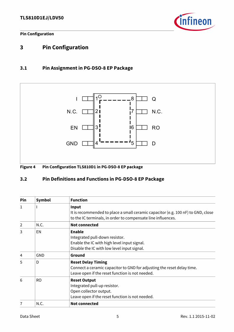
3 Pin Configuration
3.1 Pin Assignment in PG-DSO-8 EP Package
Figure 4 Pin Configuration TLS810D1 in PG-DSO-8 EP package
3.2 Pin Definitions and Functions in PG-DSO-8 EP Package
Pin Symbol Function1 I Input
It is recommended to place a small ceramic capacitor (e.g. 100 nF) to GND, close to the IC terminals, in order to compensate line influences.
2 N.C. Not connected3 EN Enable
Integrated pull-down resistor.Enable the IC with high level input signal.Disable the IC with low level input signal.
4 GND Ground5 D Reset Delay Timing
Connect a ceramic capacitor to GND for adjusting the reset delay time.Leave open if the reset function is not needed.
6 RO Reset OutputIntegrated pull-up resistor.Open collector output.Leave open if the reset function is not needed.
7 N.C. Not connected
Q
N.C.
RO
I
N.C.
EN
GND D
1
3
2
8
7
6
4 5

Data Sheet 6 Rev. 1.1 2015-11-02
TLS810D1EJ/LDV50
Pin Configuration
3.3 Pin Assignment in PG-TSON-10 Package
Figure 5 Pin Configuration TLS810D1 in PG-TSON-10 package
3.4 Pin Definitions and Functions in PG-TSON-10 Package
8 Q OutputConnect an output capacitor CQ to GND close to the IC’s terminals, respecting the values specified for its capacitance and ESR in Table 2 “Functional Range” on Page 9.
Pad – Exposed PadConnect to heatsink area.Connect to GND.
Pin Symbol Function1 I Input
It is recommended to place a small ceramic capacitor (e.g. 100 nF) to GND, close to the IC terminals, in order to compensate line influences.
2 N.C. Not connected3 EN Enable
Integrated pull-down resistor.Enable the IC with high level input signal.Disable the IC with low level input signal.
4 N.C. Not connected5 GND Ground
Pin Symbol Function
I N.C.
N.C.
EN
GND
N.C.
D
1
2
3
TSON-10
5
10
9
8
7
6
N.C.
Q
RO4

Data Sheet 7 Rev. 1.1 2015-11-02
TLS810D1EJ/LDV50
Pin Configuration
6 D Reset Delay TimingConnect a ceramic capacitor to GND for adjusting the reset delay time.Leave open if the reset function is not needed.
7 RO Reset OutputIntegrated pull-up resistor.Open collector output.Leave open if the reset function is not needed.
8 N.C. Not connected9 Q Output
Connect an output capacitor CQ to GND close to the IC’s terminals, respecting the values specified for its capacitance and ESR in Table 2 “Functional Range” on Page 9.
10 N.C. Not connectedPad – Exposed Pad
Connect to heatsink area.Connect to GND.
Pin Symbol Function

Data Sheet 8 Rev. 1.1 2015-11-02
TLS810D1EJ/LDV50
General Product Characteristics
4 General Product Characteristics
4.1 Absolute Maximum Ratings
Notes1. Stresses above the ones listed here may cause permanent damage to the device. Exposure to absolute
maximum rating conditions for extended periods may affect device reliability.2. Integrated protection functions are designed to prevent IC destruction under fault conditions described in the
data sheet. Fault conditions are considered as “outside” normal operating range. Protection functions are not designed for continuous repetitive operation.
Table 1 Absolute Maximum Ratings1)
Tj = -40 °C to +150 °C; all voltages with respect to ground (unless otherwise specified)
1) Not subject to production testing, specified by design.
Parameter Symbol Values Unit Note or Test Condition
NumberMin. Typ. Max.
Voltage Input I, Enable ENVoltage VI, VEN -0.3 – 45 V – P_4.1.1
Voltage Output QVoltage VQ -0.3 – 7 V – P_4.1.2
Reset Output RO, Reset Delay DVoltage VRO, VD -0.3 – 7 V – P_4.1.3
TemperaturesJunction Temperature Tj -40 – 150 °C – P_4.1.4
Storage Temperature Tstg -55 – 150 °C – P_4.1.5
ESD AbsorptionESD Susceptibility to GND VESD,HBM -2 – 2 kV HBM2)
2) ESD susceptibility, HBM according to ANSI/ESDA/JEDEC JS001 (1.5 kΩ, 100 pF)
P_4.1.6
ESD Susceptibility to GND VESD,CDM -750 – 750 V CDM3) at all pins
3) ESD susceptibility, Charged Device Model “CDM” according JEDEC JESD22-C101
P_4.1.7

Data Sheet 9 Rev. 1.1 2015-11-02
TLS810D1EJ/LDV50
General Product Characteristics
4.2 Functional Range
Note: Within the functional or operating range, the IC operates as described in the circuit description. The electrical characteristics are specified within the conditions given in the Electrical Characteristics table.
Table 2 Functional RangeParameter Symbol Values Unit Note or
Test ConditionNumber
Min. Typ. Max.Input Voltage Range VI VQ,nom+Vdr – 42 V –1)
1) Output current is limited internally and depends on the input voltage, see Electrical Characteristics for more details.
P_4.2.1
Extended Input Voltage Range VI,ext 2.75 – 42 V –2)
2) When VI is between VI,ext.min and VQ,nom + Vdr, VQ = VI - Vdr. When VI is below VI,ext,min, VQ can drop down to 0 V.
P_4.2.2
Output Capacitor CQ 1 – – µF –3)4)
3) The minimum output capacitance requirement is applicable for a worst case capacitance tolerance of 30%.
P_4.2.3
Output Capacitor’s ESR ESR(CQ) – – 100 Ω –4)
4) Not subject to production testing, specified by design.
P_4.2.4
Junction temperature Tj -40 – 150 °C – P_4.2.5

Data Sheet 10 Rev. 1.1 2015-11-02
TLS810D1EJ/LDV50
General Product Characteristics
4.3 Thermal Resistance
Note: This thermal data was generated in accordance with JEDEC JESD51 standards. For more information, go to www.jedec.org.
Table 3 Thermal Resistance TLS810D1 in PG-DSO-8 EP PackageParameter Symbol Values Unit Note or
Test ConditionNumber
Min. Typ. Max.Package Version Junction to Case1)
1) Not subject to production test, specified by design
RthJC – 19 – K/W – P_4.3.1
Junction to Ambient RthJA – 51 – K/W 2s2p board2)
2) Specified RthJA value is according to Jedec JESD51-2,-5,-7 at natural convection on FR4 2s2p board; The Product (Chip+Package) was simulated on a 76.2 x 114.3 x 1.5 mm³ board with 2 inner copper layers (2 x 70µm Cu, 2 x 35µm Cu). Where applicable a thermal via array under the exposed pad contacted the first inner copper layer.
P_4.3.2
Junction to Ambient RthJA – 167 – K/W 1s0p board, footprint only3)
3) Specified RthJA value is according to JEDEC JESD 51-3 at natural convection on FR4 1s0p board; The Product (Chip+Package) was simulated on a 76.2 × 114.3 × 1.5 mm3 board with 1 copper layer (1 x 70µm Cu).
P_4.3.3
Junction to Ambient RthJA – 71 – K/W 1s0p board, 300 mm2 heatsink area on PCB3)
P_4.3.4
Junction to Ambient RthJA – 60 – K/W 1s0p board, 600 mm2 heatsink area on PCB3)
P_4.3.5
Table 4 Thermal Resistance TLS810D1 in PG-TSON-10 PackageParameter Symbol Values Unit Note or
Test ConditionNumber
Min. Typ. Max.Package Version Junction to Case1)
1) Not subject to production test, specified by design
RthJC – 13 – K/W – P_4.3.6
Junction to Ambient RthJA – 60 – K/W 2s2p board2)
2) Specified RthJA value is according to Jedec JESD51-2,-5,-7 at natural convection on FR4 2s2p board; The Product (Chip+Package) was simulated on a 76.2 x 114.3 x 1.5 mm³ board with 2 inner copper layers (2 x 70µm Cu, 2 x 35µm Cu). Where applicable a thermal via array under the exposed pad contacted the first inner copper layer.
P_4.3.7
Junction to Ambient RthJA – 184 – K/W 1s0p board, footprint only3)
3) Specified RthJA value is according to JEDEC JESD 51-3 at natural convection on FR4 1s0p board; The Product (Chip+Package) was simulated on a 76.2 × 114.3 × 1.5 mm3 board with 1 copper layer (1 x 70µm Cu).
P_4.3.8
Junction to Ambient RthJA – 75 – K/W 1s0p board, 300 mm2 heatsink area on PCB3)
P_4.3.9
Junction to Ambient RthJA – 64 – K/W 1s0p board, 600 mm2 heatsink area on PCB3)
P_4.3.10
Data Sheet 11 Rev. 1.1 2015-11-02
TLS810D1EJ/LDV50
Block Description and Electrical Characteristics
5 Block Description and Electrical Characteristics
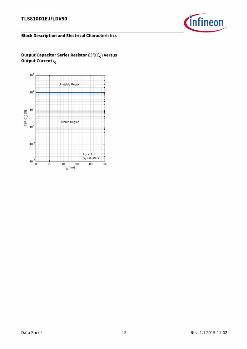
5.1 Voltage RegulationThe output voltage VQ is divided by a resistor network. This fractional voltage is compared to an internalvoltage reference and the pass transistor is driven accordingly.The control loop stability depends on the output capacitor CQ, the load current, the chip temperature and theinternal circuit structure. To ensure stable operation, the output capacitor’s capacitance and its equivalentseries resistor ESR requirements given in “Functional Range” on Page 9 have to be maintained. For detailssee the typical performance graph Output Capacitor Series Resistor ESR(CQ) versus Output Current IQ.Since the output capacitor is used to buffer load steps, it should be sized according to the application’s needs.An input capacitor CI is not required for stability, but is recommended to compensate line fluctuations. Anadditional reverse polarity protection diode and a combination of several capacitors for filtering should beused, in case the input is connected directly to the battery line. Connect the capacitors close to the regulatorterminals.In order to prevent overshoots during start-up, a smooth ramping up function is implemented. This ensuresalmost no overshoots during start-up, mostly independent from load and output capacitance.Whenever the load current exceeds the specified limit, e.g. in case of a short circuit, the output current islimited and the output voltage decreases. The overtemperature shutdown circuit prevents the IC from immediate destruction under fault conditions(e.g. output continuously short-circuit) by switching off the power stage. After the chip has cooled down, theregulator restarts. This oscillatory thermal behaviour causes the junction temperature to exceed themaximum rating of 150°C and can significantly reduce the IC’s lifetime.
Figure 6 Block Diagram Voltage Regulation
Bandgap Reference
GND
QI
Temperature Shutdown
Current Limitation
Regulated Output VoltageIQ
VQCQ
Supply
VI LOAD
C
ESRCI
II
Data Sheet 12 Rev. 1.1 2015-11-02
TLS810D1EJ/LDV50
Block Description and Electrical Characteristics
Table 5 Electrical CharacteristicsTj = -40 °C to +150 °C, VI = 13.5 V, all voltages with respect to ground (unless otherwise specified).Typical values are given at Tj = 25 °C, VI = 13.5 V.
Parameter Symbol Values Unit Note or Test Condition NumberMin. Typ. Max.
Output Voltage Precision VQ 4.90 5.00 5.10 V 50 µA ≤ IQ ≤ 100 mA, 5.7 V ≤ VI ≤ 28 V
P_5.1.1
Output Voltage Precision VQ 4.90 5.00 5.10 V 50 µA ≤ IQ ≤ 50 mA, 5.7 V ≤ VI ≤ 42 V
P_5.1.2
Output Current Limitation IQ,lim 110 190 260 mA 0 V ≤ VQ ≤ VQ,nom - 0.1 V P_5.1.3
Line Regulationsteady-state
ΔVQ,line – 1 20 mV IQ = 1 mA, 6 V ≤ VI ≤ 32 V P_5.1.4
Load Regulationsteady-state
ΔVQ,load -20 -1 – mV VI = 6 V, 50 µA ≤ IQ ≤ 100 mA
P_5.1.5
Dropout Voltage1)
Vdr = VI - VQ
1) Measured when the output voltage VQ has dropped 100 mV from the nominal value obtained at VI = 13.5V
Vdr – 200 550 mV IQ = 100 mA P_5.1.6
Ripple Rejection2)
2) Not subject to production test, specified by design
PSRR – 55 – dB IQ = 50 mA,fripple = 100 Hz,Vripple = 0.5 Vp-p
P_5.1.7
Overtemperature Shutdown Threshold
Tj,sd 151 175 – °C Tj increasing P_5.1.8
Overtemperature Shutdown Threshold Hysteresis
Tj,sdh – 10 – K Tj decreasing P_5.1.9

Data Sheet 13 Rev. 1.1 2015-11-02
TLS810D1EJ/LDV50
Block Description and Electrical Characteristics
5.2 Typical Performance Characteristics Voltage Regulation
Typical Performance Characteristics
Output Voltage VQ versusJunction Temperature Tj
Output Current IQ versusInput Voltage VI
Dropout Voltage Vdr versusJunction Temperature Tj
Dropout Voltage Vdr versusOutput Current IQ
0 50 100 1504.8
4.85
4.9
4.95
5
5.05
5.1
5.15
Tj [°C]
VQ
[V]
VI = 13.5 VIQ = 50 mA
0 10 20 30 400
50
100
150
200
250
300
VI [V]
I Qm
ax [m
A]
Tj = −40 °C
Tj = 25 °C
Tj = 150 °C
0 50 100 1500
50
100
150
200
250
300
350
400
Tj [°C]
Vdr
[mV
]
IQ = 10 mA
IQ = 50 mA
IQ = 100 mA
0 20 40 60 80 1000
50
100
150
200
250
300
350
400
IQ [mA]
Vdr
[mV
]
Tj = −40 °C
Tj = 25 °C
Tj = 150 °C

Data Sheet 14 Rev. 1.1 2015-11-02
TLS810D1EJ/LDV50
Block Description and Electrical Characteristics
Load Regulation ΔVQ,load versus Output Current IQ
Line Regulation ΔVQ,line versus Input Voltage VI
Output Voltage VQ versusInput Voltage VI
Power Supply Ripple Rejection PSRR versusRipple Frequency fr
0 20 40 60 80 100−10
−8
−6
−4
−2
0
2
4
6
8
10
IQ [mA]
dVlo
ad [m
V]
VI = 6 V
Tj = −40 °C
Tj = 25 °C
Tj = 150 °C
10 15 20 25 30 35 40−10
−8
−6
−4
−2
0
2
4
6
8
10
VI [V]
dVlin
e [mV
]
IQ = 1 mA
Tj = −40 °C
Tj = 25 °C
Tj = 150 °C
0 1 2 3 4 5 60
1
2
3
4
5
6
VI [V]
VQ
[V]
IQ = 50 mATj = 25 °C
10−2 10−1 100 101 102 1030
10
20
30
40
50
60
70
80
f [kHz]
PS
RR
[dB
]
IQ = 10 mACQ = 1 μFVI = 13.5 VVripple = 0.5 VppTj = 25 °C
Data Sheet 15 Rev. 1.1 2015-11-02
TLS810D1EJ/LDV50
Block Description and Electrical Characteristics
Output Capacitor Series Resistor ESR(CQ) versusOutput Current IQ
0 20 40 60 80 10010−2
10−1
100
101
102
103
IQ [mA]
ES
R(C
Q)
[Ω]
CQ = 1 μFVI = 3...28 V
Stable Region
Unstable Region

Data Sheet 16 Rev. 1.1 2015-11-02
TLS810D1EJ/LDV50
Block Description and Electrical Characteristics
5.3 Current Consumption
Table 6 Electrical Characteristics Current ConsumptionTj = -40 °C to +150 °C, VI = 13.5 V (unless otherwise specified).
Parameter Symbol Values Unit Note or Test Condition NumberMin. Typ. Max.
Current ConsumptionIq = II
Iq,off – – 1 µA VEN ≤ 0.4 V, Tj < 105 °C P_5.3.1
Current ConsumptionIq = II - IQ
Iq – 9 11.5 µA IQ = 50 µA, Tj = 25 °C P_5.3.2
Current ConsumptionIq = II - IQ
Iq – 11.5 14.5 µA IQ = 50 µA, Tj < 105 °C P_5.3.3
Current ConsumptionIq = II - IQ
Iq – 12 16 µA IQ = 50 µA, Tj < 125 °C P_5.3.4
Current ConsumptionIq = II - IQ
Iq – 12 16 µA IQ= 100 mA, Tj < 125 °C P_5.3.5

Data Sheet 17 Rev. 1.1 2015-11-02
TLS810D1EJ/LDV50
Block Description and Electrical Characteristics
5.4 Typical Performance Characteristics Current Consumption
Typical Performance Characteristics
Current Consumption Iq versusOutput Current IQ
Current Consumption Iq versusInput Voltage VI
Current Consumption Iq versusJunction Temperature Tj
Current Consumption in OFF mode Iq,off versusJunction Temperature Tj
0 20 40 60 80 1000
4
8
12
16
20
24
IQ [mA]
I q [μA
]
VI = 13.5 V
Tj = −40 °C
Tj = 25 °C
Tj = 105 °C
Tj = 125 °C
10 15 20 25 30 35 400
5
10
15
20
25
30
35
40
VI [V]
I q [μA
]
IQ = 50 μA
Tj = −40 °C
Tj = 25 °C
Tj = 105 °C
Tj = 125 °C
0 50 100 1500
4
8
12
16
20
24
Tj [°C]
I q [μA
]
VI = 13.5 VIQ = 50 μA
0 50 100 1500
0.5
1
1.5
2
2.5
3
3.5
4
Tj [°C]
I q,of
f [μA
]
VI = 13.5 VVEN ≤ 0.4 V

Data Sheet 18 Rev. 1.1 2015-11-02
TLS810D1EJ/LDV50
Block Description and Electrical Characteristics
5.5 EnableThe device can be switched on and off by the Enable feature. Connect a HIGH level as specified below (e.g. thebattery voltage) to pin EN to enable the device; connect a LOW level as specified below (e.g. GND) to switch itoff. The Enable function has a build-in hysteresis to avoid toggling between ON/OFF state, if signals with slowslopes are appiled to the EN input.
Table 7 Electrical Characteristics Enable Tj = -40 °C to +150 °C, VI = 13.5 V, all voltages with respect to ground (unless otherwise specified). Typical values are given at Tj = 25 °C, VI = 13.5 V.
Parameter Symbol Values Unit Note or Test Condition NumberMin. Typ. Max.
Enable High Level Input Voltage
VEN,H 2 – – V VQ settled P_5.5.1
Enable Low Level Input Voltage
VEN,L – – 0.8 V VQ ≤ 0.1 V P_5.5.2
Enable High Level Input Current
IEN,H – – 4 µA VEN = 5 V P_5.5.3
Enable Internal Pull-down Resistor
REN 1.25 2 3.5 MΩ – P_5.5.4

Data Sheet 19 Rev. 1.1 2015-11-02
TLS810D1EJ/LDV50
Block Description and Electrical Characteristics
5.6 Typical Performance Characteristics Enable
Typical Performance Characteristics
Enable Input Current IEN versusEnable Input Voltage VEN
0 10 20 30 400
5
10
15
20
25
30
35
40
VEN [V]
I EN [μ
A]
Tj = −40 °C
Tj = 25 °C
Tj = 150 °C
Data Sheet 20 Rev. 1.1 2015-11-02
TLS810D1EJ/LDV50
Block Description and Electrical Characteristics
5.7 Reset FunctionThe reset function provides several features:
Output Undervoltage Reset An output undervoltage condition is indicated by setting the Reset Output RO to “low”. This signal may beused to reset a microcontroller during low supply voltage.
Power-On Reset Delay TimeThe power-on reset delay time trd allows microcontoller and oscillator to start up. This delay time is the timeframe from exceeding the reset switching threshold VRT until the reset is released by switching the reset output“RO” from “low” to “high”. The power-on reset delay time trd is defined by an external delay capacitor CDconnected to pin D charged by the delay capacitor charge current ID,ch starting from VD = 0 V.If the application needs a power-on reset delay time trd different from the value given in Table 8, the delaycapacitor’s value can be derived from the specified value and the desired power-on delay time:
(5.1)
with• CD: capacitance of the delay capacitor to be chosen• trd,new: desired power-on reset delay time• trd: power-on reset delay time specified in this datasheetFor a precise calculation also take the delay capacitor’s tolerance into consideration.
Reset Reaction TimeThe reset reaction rime trr considers the internal reaction time trr,int and the discharge time trr,d defined by theexternal delay capacitor CD (see typical performance graph for details). Hence, the total reset reaction timebecomes:
(5.2)
with• trr: reset reaction time• trr,int: internal reset reaction time• trr,d: reset discharge
Optional Reset Output Pull-Up Resistor RRO,ext
The Reset Output RO is an open collector output with an integrated pull-up resistor. If needed, an externalpull-up resistor to the output Q can be added. In Table 8 a minimum value for the external resistor RRO,ext isgiven.
•CD =trd,new
100 nFtrd
trr = +trr,int trr,d

Data Sheet 21 Rev. 1.1 2015-11-02
TLS810D1EJ/LDV50
Block Description and Electrical Characteristics
Figure 7 Block Diagram Reset Function
GND
QISupply
RO
VDST
Int. Supply
ID,ch
ID,dch
VRADJ ,th
Control
D
CD
Reset
optio
nal
CQ
VDD
Micro-Controller
GND
RRO
IRO
RRO ,ext

Data Sheet 22 Rev. 1.1 2015-11-02
TLS810D1EJ/LDV50
Block Description and Electrical Characteristics
Figure 8 Timing Diagram Reset
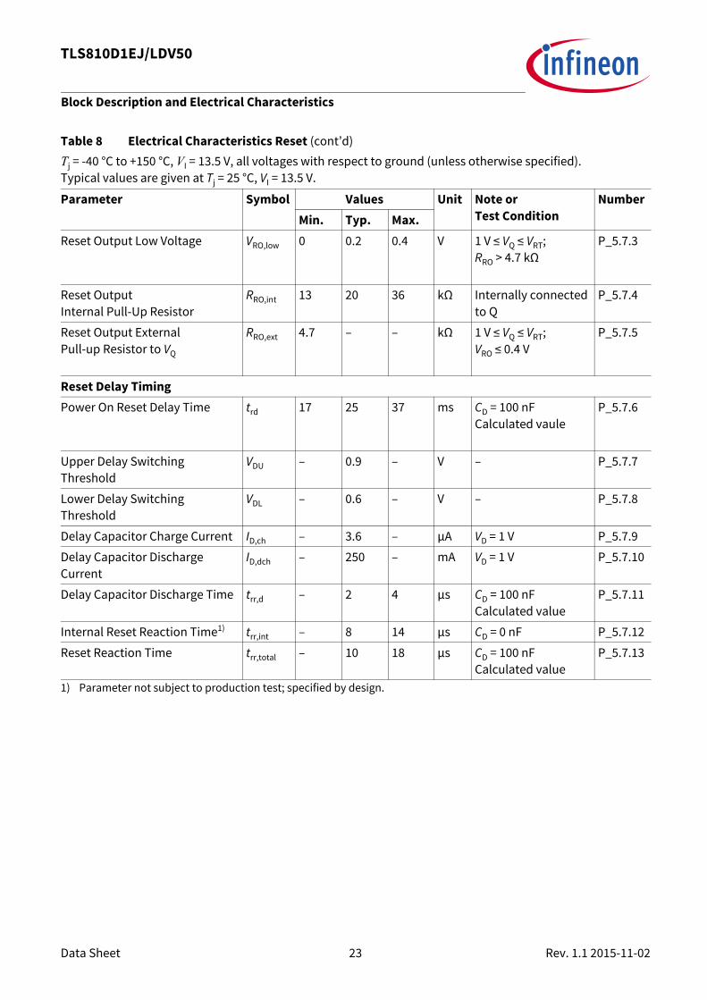
Table 8 Electrical Characteristics ResetTj = -40 °C to +150 °C, VI = 13.5 V, all voltages with respect to ground (unless otherwise specified).Typical values are given at Tj = 25 °C, VI = 13.5 V.
Parameter Symbol Values Unit Note or Test Condition
NumberMin. Typ. Max.
Output Undervoltage ResetOutput Undervoltage Reset Upper Switching Threshold
VRT,high 4.6 4.7 4.8 V VQ increasing, VEN ≥ 2.0 V
P_5.7.1
Output Undervoltage Reset Lower Switching Threshold
VRT,low 4.5 4.6 4.7 V VQ decreasing, VEN ≥ 2.0 V
P_5.7.2
Reset Output RO
VI
t
VQ
t
VRT,high
VRO
TimingDiagram_Reset.vsd
tVRO,low
1 V
1V
trr,totaltrd
Thermal Shutdown
Input Voltage Dip
trr,totaltrd trd
t < trr,total
trd
Under-voltage
Spike at output
Over-load
trr,total
VDRL
VDU
t
VD
VRT,low
Data Sheet 23 Rev. 1.1 2015-11-02
TLS810D1EJ/LDV50
Block Description and Electrical Characteristics
Reset Output Low Voltage VRO,low 0 0.2 0.4 V 1 V ≤ VQ ≤ VRT; RRO > 4.7 kΩ
P_5.7.3
Reset Output Internal Pull-Up Resistor
RRO,int 13 20 36 kΩ Internally connected to Q
P_5.7.4
Reset Output ExternalPull-up Resistor to VQ
RRO,ext 4.7 – – kΩ 1 V ≤ VQ ≤ VRT;VRO ≤ 0.4 V
P_5.7.5
Reset Delay TimingPower On Reset Delay Time trd 17 25 37 ms CD = 100 nF
Calculated vauleP_5.7.6
Upper Delay Switching Threshold
VDU – 0.9 – V – P_5.7.7
Lower Delay Switching Threshold
VDL – 0.6 – V – P_5.7.8
Delay Capacitor Charge Current ID,ch – 3.6 – µA VD = 1 V P_5.7.9
Delay Capacitor Discharge Current
ID,dch – 250 – mA VD = 1 V P_5.7.10
Delay Capacitor Discharge Time trr,d – 2 4 µs CD = 100 nFCalculated value
P_5.7.11
Internal Reset Reaction Time1) trr,int – 8 14 µs CD = 0 nF P_5.7.12
Reset Reaction Time trr,total – 10 18 µs CD = 100 nFCalculated value
P_5.7.13
1) Parameter not subject to production test; specified by design.
Table 8 Electrical Characteristics Reset (cont’d)Tj = -40 °C to +150 °C, VI = 13.5 V, all voltages with respect to ground (unless otherwise specified).Typical values are given at Tj = 25 °C, VI = 13.5 V.
Parameter Symbol Values Unit Note or Test Condition
NumberMin. Typ. Max.

Data Sheet 24 Rev. 1.1 2015-11-02
TLS810D1EJ/LDV50
Block Description and Electrical Characteristics
5.8 Typical Performance Characteristics Reset
Typical Performance Characteristics
Undervoltage Reset Threshold VRT versusJunction Temperature Tj
Power On Reset Delay Time trd versusJunction Temperature Tj
Internal Reset Reaction Time trr,int versusJunction Temperature Tj
0 50 100 1504.5
4.55
4.6
4.65
4.7
4.75
4.8
4.85
4.9
4.95
5
Tj [°C]
VR
T [V]
VRT high
VRT low
0 50 100 1500
5
10
15
20
25
30
35
40
Tj [°C]
t rd [m
s]
CD = 100 nF
0 50 100 1500
2
4
6
8
10
12
14
16
Tj [°C]
t rr,in
t [μs]
Data Sheet 25 Rev. 1.1 2015-11-02
TLS810D1EJ/LDV50
Application Information
6 Application Information
Note: The following information is given as a hint for the implementation of the device only and shall not be regarded as a description or warranty of a certain functionality, condition or quality of the device.
6.1 Application Diagram
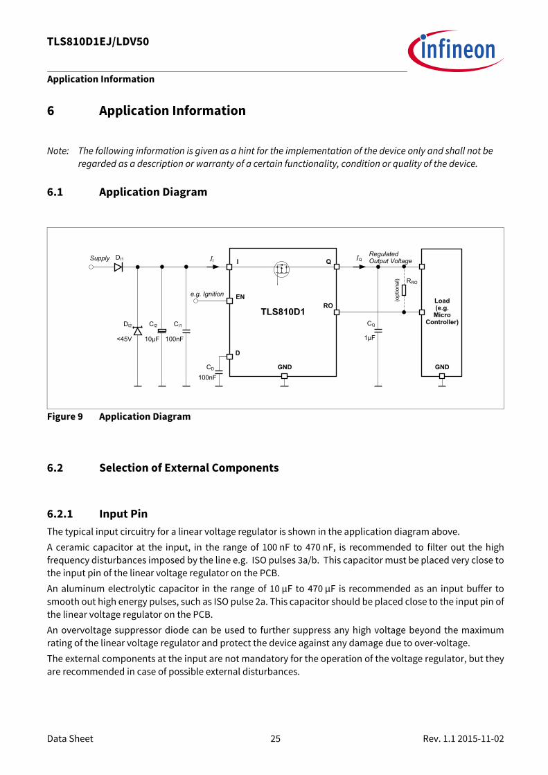
Figure 9 Application Diagram
6.2 Selection of External Components
6.2.1 Input PinThe typical input circuitry for a linear voltage regulator is shown in the application diagram above.A ceramic capacitor at the input, in the range of 100 nF to 470 nF, is recommended to filter out the highfrequency disturbances imposed by the line e.g. ISO pulses 3a/b. This capacitor must be placed very close tothe input pin of the linear voltage regulator on the PCB. An aluminum electrolytic capacitor in the range of 10 µF to 470 µF is recommended as an input buffer tosmooth out high energy pulses, such as ISO pulse 2a. This capacitor should be placed close to the input pin ofthe linear voltage regulator on the PCB.An overvoltage suppressor diode can be used to further suppress any high voltage beyond the maximumrating of the linear voltage regulator and protect the device against any damage due to over-voltage.The external components at the input are not mandatory for the operation of the voltage regulator, but theyare recommended in case of possible external disturbances.
TLS810D1
QI
ENRO
D
Regulated Output VoltageIQ
CQ
1μF
CD
100nF
Supply
100nF10μF
CI1CI2
<45V
DI2
II
GND
e.g. IgnitionLoad(e.g.
Micro Controller)
GND
(opt
iona
l) RRO
DI1
Data Sheet 26 Rev. 1.1 2015-11-02
TLS810D1EJ/LDV50
Application Information
6.2.2 Output PinAn output capacitor is mandatory for the stability of linear voltage regulators. The requirement to the output capacitor is given in “Functional Range” on Page 9. The graph “OutputCapacitor Series Resistor ESR(CQ) versus Output Current IQ” on Page 15 shows the stable operation rangeof the device.TLS810D1 is designed to be stable with extremely low ESR capacitors. According to the automotiveenvironment, ceramic capacitors with X5R or X7R dielectrics are recommended.The output capacitor should be placed as close as possible to the regulator’s output and GND pins and on thesame side of the PCB as the regulator itself.In case of rapid transients of input voltage or load current, the capacitance should be dimensioned inaccordance and verified in the real application that the output stability requirements are fulfilled.
6.3 Thermal ConsiderationsKnowing the input voltage, the output voltage and the load profile of the application, the total powerdissipation can be calculated:
(6.1)
with• PD: continuous power dissipation• VI: input voltage• VQ: output voltage• IQ: output current• Iq: quiescent current
The maximum acceptable thermal resistance RthJA can then be calculated:
(6.2)
with• Tj,max: maximum allowed junction temperature• Ta: ambient temperature
Based on the above calculation the proper PCB type and the necessary heat sink area can be determined withreference to the specification in “Thermal Resistance” on Page 10.
ExampleApplication conditions:VI = 13.5 VVQ = 5 VIQ = 80 mATa = 105 °C
PD VI VQ–( ) IQ VI Iq×+×=
RthJA max,Tj max, Ta–
PD----------------------------=

Data Sheet 27 Rev. 1.1 2015-11-02
TLS810D1EJ/LDV50
Application Information
Calculation of RthJA,max:PD = (VI – VQ) x IQ + VI x Iq
= (13.5V – 5V) x 80 mA + 13.5 V x 0.016 mA= 0.68 W
RthJA,max= (Tj,max – Ta) / PD
= (150 °C – 105 °C) / 0.68 W = 66.2 K/W
As a result, the PCB design must ensure a thermal resistance RthJA lower than 66.2 K/W. According to “ThermalResistance” on Page 10, for both TLS810D1EJV50 and TLS810D1LDV50 at least 600 mm² heatsink area isneeded on the FR4 1s0p PCB, or the FR4 2s2p board can be used.
6.4 Reverse Polarity ProtectionTLS810D1 is not self protected against reverse polarity faults. To protect the device against negative supplyvoltage, an external reverse polarity diode is needed, as shown in Figure 9. The absolute maximum ratings ofthe device as specified in “Absolute Maximum Ratings” on Page 8 must be kept.
6.5 Further Application Information
• For further information you may contact http://www.infineon.com/
Data Sheet 28 Rev. 1.1 2015-11-02
TLS810D1EJ/LDV50
Package Outlines
7 Package Outlines
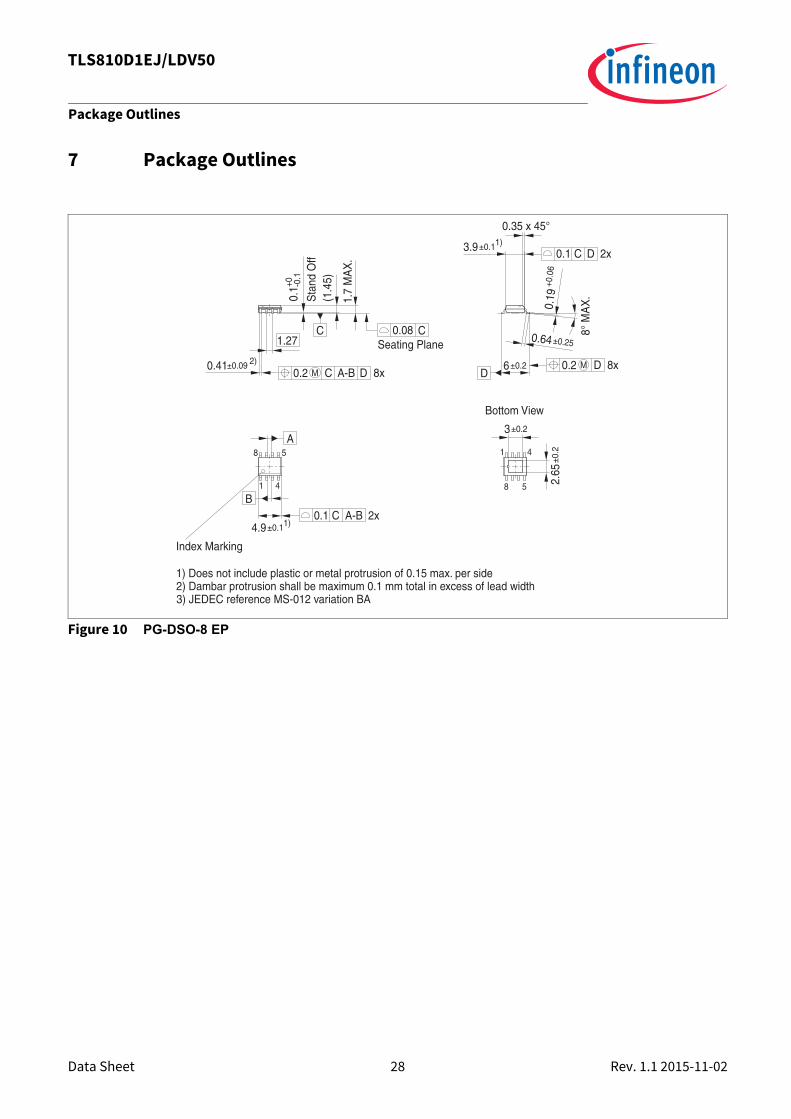
Figure 10 PG-DSO-8 EP
1 4
8 5
8
1 4
5
8x0.41±0.09 2)
M0.2 DC A-B
1.27C
Sta
nd O
ff
+0 -0.1
0.1
(1.4
5)
1.7
MA
X.
0.08Seating Plane
C
A
B
4.9±0.11)A-BC0.1 2x
3) JEDEC reference MS-012 variation BA
1) Does not include plastic or metal protrusion of 0.15 max. per side 2) Dambar protrusion shall be maximum 0.1 mm total in excess of lead width
Bottom View
±0.23
±0.2
2.65
0.2±0.2D
6 M D 8x
0.64±0.25
3.9±0.11)0.1
0.35 x 45°
C D 2x
+0.0
60.
19
8° M
AX
.
Index Marking
Data Sheet 29 Rev. 1.1 2015-11-02
TLS810D1EJ/LDV50
Package Outlines
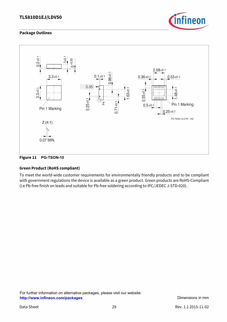
Figure 11 PG-TSON-10
Green Product (RoHS compliant)To meet the world-wide customer requirements for environmentally friendly products and to be compliantwith government regulations the device is available as a green product. Green products are RoHS-Compliant(i.e Pb-free finish on leads and suitable for Pb-free soldering according to IPC/JEDEC J-STD-020).
Pin 1 MarkingPin 1 Marking
PG-TSON-10-2-PO V02
±0.1
0.2
±0.1
0.25
±0.1
0.55
0.96
±0.1
2.58±0.10
+0.0
5
0.1 ±0.10.36 ±0.10.53
±0.1
±0.1
0.25
0.5
±0.1
3.3
±0.13.3 ±0.1
1±0.
1
0.71
±0.1
1.63
±0.1
1.48
±0.1
Z
0.05
0.07 MIN.
Z (4:1)
For further information on alternative packages, please visit our website:http://www.infineon.com/packages. Dimensions in mm

Data Sheet 30 Rev. 1.1 2015-11-02
TLS810D1EJ/LDV50
Revision History
8 Revision History
Revision Date Changes1.1 2015-11-02 - New variant TLS810D1LDV50 in PG-TSON-10 package added.
- Document style updated.- Typical performance graph Load Regulation updated.- Editorial changes.
1.0 2015-01-27 Datasheet - Initial Version

Trademarks of Infineon Technologies AGAURIX™, C166™, CanPAK™, CIPOS™, CIPURSE™, CoolMOS™, CoolSET™, CORECONTROL™, CROSSAVE™, DAVE™, DI-POL™, EasyPIM™, EconoBRIDGE™,EconoDUAL™, EconoPIM™, EconoPACK™, EiceDRIVER™, eupec™, FCOS™, HITFET™, HybridPACK™, I²RF™, ISOFACE™, IsoPACK™, LITIX™, MIPAQ™,ModSTACK™, my-d™, NovalithIC™, OptiMOS™, ORIGA™, POWERCODE™, PRIMARION™, PrimePACK™, PrimeSTACK™, PRO-SIL™, PROFET™, RASIC™,ReverSave™, SatRIC™, SIEGET™, SINDRION™, SIPMOS™, SmartLEWIS™, SPOC™, SOLID FLASH™, TEMPFET™, thinQ!™, TRENCHSTOP™, TriCore™.Other TrademarksAdvance Design System™ (ADS) of Agilent Technologies, AMBA™, ARM™, MULTI-ICE™, KEIL™, PRIMECELL™, REALVIEW™, THUMB™, µVision™ of ARM Limited,UK. AUTOSAR™ is licensed by AUTOSAR development partnership. Bluetooth™ of Bluetooth SIG Inc. CAT-iq™ of DECT Forum. COLOSSUS™, FirstGPS™ ofTrimble Navigation Ltd. EMV™ of EMVCo, LLC (Visa Holdings Inc.). EPCOS™ of Epcos AG. FLEXGO™ of Microsoft Corporation. FlexRay™ is licensed by FlexRayConsortium. HYPERTERMINAL™ of Hilgraeve Incorporated. IEC™ of Commission Electrotechnique Internationale. IrDA™ of Infrared Data AssociationCorporation. ISO™ of INTERNATIONAL ORGANIZATION FOR STANDARDIZATION. MATLAB™ of MathWorks, Inc. MAXIM™ of Maxim Integrated Products, Inc.MICROTEC™, NUCLEUS™ of Mentor Graphics Corporation. MIPI™ of MIPI Alliance, Inc. MIPS™ of MIPS Technologies, Inc., USA. muRata™ of MURATAMANUFACTURING CO., MICROWAVE OFFICE™ (MWO) of Applied Wave Research Inc., OmniVision™ of OmniVision Technologies, Inc. Openwave™ OpenwaveSystems Inc. RED HAT™ Red Hat, Inc. RFMD™ RF Micro Devices, Inc. SIRIUS™ of Sirius Satellite Radio Inc. SOLARIS™ of Sun Microsystems, Inc. SPANSION™ ofSpansion LLC Ltd. Symbian™ of Symbian Software Limited. TAIYO YUDEN™ of Taiyo Yuden Co. TEAKLITE™ of CEVA, Inc. TEKTRONIX™ of Tektronix Inc.TOKO™ of TOKO KABUSHIKI KAISHA TA. UNIX™ of X/Open Company Limited. VERILOG™, PALLADIUM™ of Cadence Design Systems, Inc. VLYNQ™ of TexasInstruments Incorporated. VXWORKS™, WIND RIVER™ of WIND RIVER SYSTEMS, INC. ZETEX™ of Diodes Zetex Limited.Last Trademarks Update 2011-11-11
Edition 2015-11-02Published by Infineon Technologies AG81726 Munich, Germany
© 2015 Infineon Technologies AG.All Rights Reserved.
Do you have a question about any aspect of this document?Email: [email protected]
Legal DisclaimerThe information given in this document shall inno event be regarded as a guarantee ofconditions or characteristics. With respect to anyexamples or hints given herein, any typicalvalues stated herein and/or any informationregarding the application of the device, InfineonTechnologies hereby disclaims any and allwarranties and liabilities of any kind, includingwithout limitation, warranties of non-infringement of intellectual property rights ofany third party.InformationFor further information on technology, deliveryterms and conditions and prices, please contactthe nearest Infineon Technologies Office(www.infineon.com).
WarningsDue to technical requirements, componentsmay contain dangerous substances. Forinformation on the types in question, pleasecontact the nearest Infineon TechnologiesOffice. Infineon Technologies components maybe used in life-support devices or systems onlywith the express written approval of InfineonTechnologies, if a failure of such componentscan reasonably be expected to cause the failureof that life-support device or system or to affectthe safety or effectiveness of that device orsystem. Life support devices or systems areintended to be implanted in the human body orto support and/or maintain and sustain and/orprotect human life. If they fail, it is reasonable toassume that the health of the user or otherpersons may be endangered.
www.infineon.com
Mouser Electronics
Authorized Distributor
Click to View Pricing, Inventory, Delivery & Lifecycle Information: Infineon:
TLS810D1EJV50XUMA1


