The S-801 Series is a series of high-precision voltage detectors with a built-in delay time generator of fixed time developed using CMOS process. The detection voltage is fixed internally, with an accuracy of 2.0 %. Internal oscillator and counter timer can delay the release signal without external parts. Three delay times 50 ms, 100 ms, and 200 ms are available. Two output forms, Nch open-drain and CMOS output, are available. Features
Ultra-low current consumption 1.3 A typ. (at VDD3.5 V) High-precision detection voltage 2.0 % Operating voltage range 0.95 V to 10.0 V Hysteresis characteristics 60 mV typ. Detection voltage 2.2 V to 6.0 V (0.1 V step) Three delay times A type 50 ms typ. B type 100 ms typ. C type 200 ms typ. ON/OFF switching function of delay time (DS pin) Output forms Nch open-drain output (Active Low) CMOS output (Active Low) Lead-free, Sn 100%, halogen-free*1
*1. Refer to “ Product Name Structure” for details.
Applications
Power monitor for portable equipment such as notebook computers, digital still cameras, PDA, and cellular phones.
Constant voltage power monitor for cameras, video equipment and communication devices. Power monitor for microcomputers and reset for CPUs.
Packages
SOT-23-5 SNT-4A
www.ablic.com
ULTRA-SMALL PACKAGE HIGH-PRECISION VOLTAGE DETECTOR WITH DELAY CIRCUIT (INTERNAL DELAY TIME SETTING) S-801 Series Rev.4.2_01
2
Block Diagrams
1. Nch Open-drain Output Products
Delay circuit
DS
Oscillator counter timer
OUT *1
VREF
VSS
VDD
*1
*1
*1. Parasitic diode
Figure 1
2. CMOS Output Products
VREF
OUT
*1
*1Delay circuit
DS
Oscillator counter timer
VSS
VDD
*1
*1
*1. Parasitic diode
Figure 2
ULTRA-SMALL PACKAGE HIGH-PRECISION VOLTAGE DETECTOR WITH DELAY CIRCUIT (INTERNAL DELAY TIME SETTING)Rev.4.2_01 S-801 Series
3
Product Name Structure
The detection voltage, delay time, output form and packages for S-801 Series can be selected at the user's request. Refer to the “1. Product name” for the construction of the product name, “2. Packages” regarding the package drawings and “3. Product Name List” for the full product names.
ULTRA-SMALL PACKAGE HIGH-PRECISION VOLTAGE DETECTOR WITH DELAY CIRCUIT (INTERNAL DELAY TIME SETTING)Rev.4.2_01 S-801 Series
5
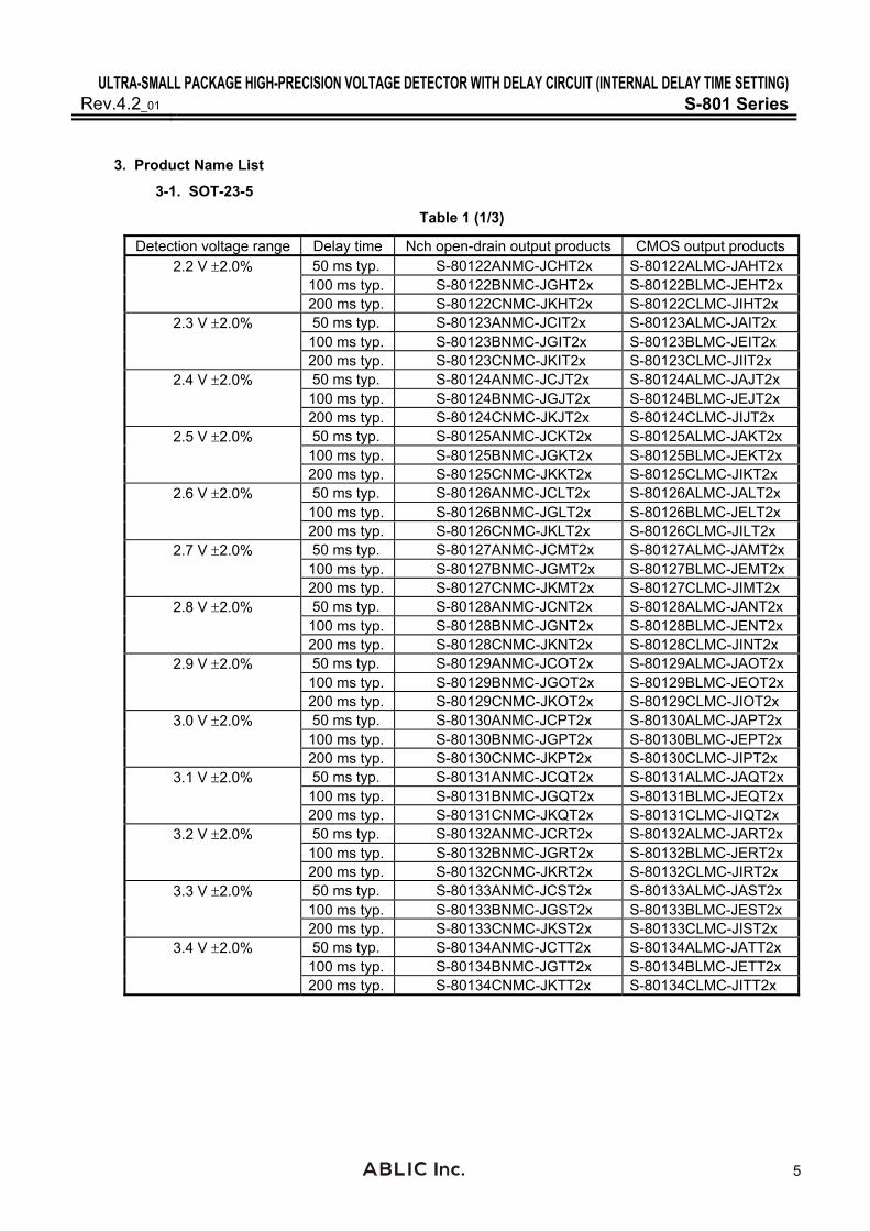
3. Product Name List
3-1. SOT-23-5
Table 1 (1/3)
Detection voltage range Delay time Nch open-drain output products CMOS output products2.2 V 2.0% 50 ms typ. S-80122ANMC-JCHT2x S-80122ALMC-JAHT2x
100 ms typ. S-80122BNMC-JGHT2x S-80122BLMC-JEHT2x 200 ms typ. S-80122CNMC-JKHT2x S-80122CLMC-JIHT2x
2.3 V 2.0% 50 ms typ. S-80123ANMC-JCIT2x S-80123ALMC-JAIT2x 100 ms typ. S-80123BNMC-JGIT2x S-80123BLMC-JEIT2x 200 ms typ. S-80123CNMC-JKIT2x S-80123CLMC-JIIT2x
2.4 V 2.0% 50 ms typ. S-80124ANMC-JCJT2x S-80124ALMC-JAJT2x 100 ms typ. S-80124BNMC-JGJT2x S-80124BLMC-JEJT2x 200 ms typ. S-80124CNMC-JKJT2x S-80124CLMC-JIJT2x
2.5 V 2.0% 50 ms typ. S-80125ANMC-JCKT2x S-80125ALMC-JAKT2x 100 ms typ. S-80125BNMC-JGKT2x S-80125BLMC-JEKT2x 200 ms typ. S-80125CNMC-JKKT2x S-80125CLMC-JIKT2x
2.6 V 2.0% 50 ms typ. S-80126ANMC-JCLT2x S-80126ALMC-JALT2x 100 ms typ. S-80126BNMC-JGLT2x S-80126BLMC-JELT2x 200 ms typ. S-80126CNMC-JKLT2x S-80126CLMC-JILT2x
2.7 V 2.0% 50 ms typ. S-80127ANMC-JCMT2x S-80127ALMC-JAMT2x 100 ms typ. S-80127BNMC-JGMT2x S-80127BLMC-JEMT2x 200 ms typ. S-80127CNMC-JKMT2x S-80127CLMC-JIMT2x
2.8 V 2.0% 50 ms typ. S-80128ANMC-JCNT2x S-80128ALMC-JANT2x 100 ms typ. S-80128BNMC-JGNT2x S-80128BLMC-JENT2x 200 ms typ. S-80128CNMC-JKNT2x S-80128CLMC-JINT2x
2.9 V 2.0% 50 ms typ. S-80129ANMC-JCOT2x S-80129ALMC-JAOT2x 100 ms typ. S-80129BNMC-JGOT2x S-80129BLMC-JEOT2x 200 ms typ. S-80129CNMC-JKOT2x S-80129CLMC-JIOT2x
3.0 V 2.0% 50 ms typ. S-80130ANMC-JCPT2x S-80130ALMC-JAPT2x 100 ms typ. S-80130BNMC-JGPT2x S-80130BLMC-JEPT2x 200 ms typ. S-80130CNMC-JKPT2x S-80130CLMC-JIPT2x
3.1 V 2.0% 50 ms typ. S-80131ANMC-JCQT2x S-80131ALMC-JAQT2x 100 ms typ. S-80131BNMC-JGQT2x S-80131BLMC-JEQT2x 200 ms typ. S-80131CNMC-JKQT2x S-80131CLMC-JIQT2x
3.2 V 2.0% 50 ms typ. S-80132ANMC-JCRT2x S-80132ALMC-JART2x 100 ms typ. S-80132BNMC-JGRT2x S-80132BLMC-JERT2x 200 ms typ. S-80132CNMC-JKRT2x S-80132CLMC-JIRT2x
3.3 V 2.0% 50 ms typ. S-80133ANMC-JCST2x S-80133ALMC-JAST2x 100 ms typ. S-80133BNMC-JGST2x S-80133BLMC-JEST2x 200 ms typ. S-80133CNMC-JKST2x S-80133CLMC-JIST2x
3.4 V 2.0% 50 ms typ. S-80134ANMC-JCTT2x S-80134ALMC-JATT2x 100 ms typ. S-80134BNMC-JGTT2x S-80134BLMC-JETT2x 200 ms typ. S-80134CNMC-JKTT2x S-80134CLMC-JITT2x
ULTRA-SMALL PACKAGE HIGH-PRECISION VOLTAGE DETECTOR WITH DELAY CIRCUIT (INTERNAL DELAY TIME SETTING) S-801 Series Rev.4.2_01
6
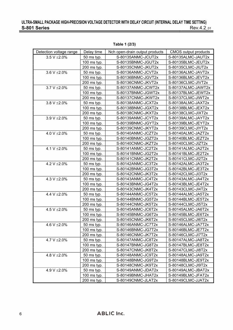
Table 1 (2/3)
Detection voltage range Delay time Nch open-drain output products CMOS output products3.5 V 2.0% 50 ms typ. S-80135ANMC-JCUT2x S-80135ALMC-JAUT2x
100 ms typ. S-80135BNMC-JGUT2x S-80135BLMC-JEUT2x 200 ms typ. S-80135CNMC-JKUT2x S-80135CLMC-JIUT2x
3.6 V 2.0% 50 ms typ. S-80136ANMC-JCVT2x S-80136ALMC-JAVT2x 100 ms typ. S-80136BNMC-JGVT2x S-80136BLMC-JEVT2x 200 ms typ. S-80136CNMC-JKVT2x S-80136CLMC-JIVT2x
3.7 V 2.0% 50 ms typ. S-80137ANMC-JCWT2x S-80137ALMC-JAWT2x 100 ms typ. S-80137BNMC-JGWT2x S-80137BLMC-JEWT2x 200 ms typ. S-80137CNMC-JKWT2x S-80137CLMC-JIWT2x
3.8 V 2.0% 50 ms typ. S-80138ANMC-JCXT2x S-80138ALMC-JAXT2x 100 ms typ. S-80138BNMC-JGXT2x S-80138BLMC-JEXT2x 200 ms typ. S-80138CNMC-JKXT2x S-80138CLMC-JIXT2x
3.9 V 2.0% 50 ms typ. S-80139ANMC-JCYT2x S-80139ALMC-JAYT2x 100 ms typ. S-80139BNMC-JGYT2x S-80139BLMC-JEYT2x 200 ms typ. S-80139CNMC-JKYT2x S-80139CLMC-JIYT2x
4.0 V 2.0% 50 ms typ. S-80140ANMC-JCZT2x S-80140ALMC-JAZT2x 100 ms typ. S-80140BNMC-JGZT2x S-80140BLMC-JEZT2x 200 ms typ. S-80140CNMC-JKZT2x S-80140CLMC-JIZT2x
4.1 V 2.0% 50 ms typ. S-80141ANMC-JC2T2x S-80141ALMC-JA2T2x 100 ms typ. S-80141BNMC-JG2T2x S-80141BLMC-JE2T2x 200 ms typ. S-80141CNMC-JK2T2x S-80141CLMC-JI2T2x
4.2 V 2.0% 50 ms typ. S-80142ANMC-JC3T2x S-80142ALMC-JA3T2x 100 ms typ. S-80142BNMC-JG3T2x S-80142BLMC-JE3T2x 200 ms typ. S-80142CNMC-JK3T2x S-80142CLMC-JI3T2x
4.3 V 2.0% 50 ms typ. S-80143ANMC-JC4T2x S-80143ALMC-JA4T2x 100 ms typ. S-80143BNMC-JG4T2x S-80143BLMC-JE4T2x 200 ms typ. S-80143CNMC-JK4T2x S-80143CLMC-JI4T2x
4.4 V 2.0% 50 ms typ. S-80144ANMC-JC5T2x S-80144ALMC-JA5T2x 100 ms typ. S-80144BNMC-JG5T2x S-80144BLMC-JE5T2x 200 ms typ. S-80144CNMC-JK5T2x S-80144CLMC-JI5T2x
4.5 V 2.0% 50 ms typ. S-80145ANMC-JC6T2x S-80145ALMC-JA6T2x 100 ms typ. S-80145BNMC-JG6T2x S-80145BLMC-JE6T2x 200 ms typ. S-80145CNMC-JK6T2x S-80145CLMC-JI6T2x
4.6 V 2.0% 50 ms typ. S-80146ANMC-JC7T2x S-80146ALMC-JA7T2x 100 ms typ. S-80146BNMC-JG7T2x S-80146BLMC-JE7T2x 200 ms typ. S-80146CNMC-JK7T2x S-80146CLMC-JI7T2x
4.7 V 2.0% 50 ms typ. S-80147ANMC-JC8T2x S-80147ALMC-JA8T2x 100 ms typ. S-80147BNMC-JG8T2x S-80147BLMC-JE8T2x 200 ms typ. S-80147CNMC-JK8T2x S-80147CLMC-JI8T2x
4.8 V 2.0% 50 ms typ. S-80148ANMC-JC9T2x S-80148ALMC-JA9T2x 100 ms typ. S-80148BNMC-JG9T2x S-80148BLMC-JE9T2x 200 ms typ. S-80148CNMC-JK9T2x S-80148CLMC-JI9T2x
4.9 V 2.0% 50 ms typ. S-80149ANMC-JDAT2x S-80149ALMC-JBAT2x 100 ms typ. S-80149BNMC-JHAT2x S-80149BLMC-JFAT2x 200 ms typ. S-80149CNMC-JLAT2x S-80149CLMC-JJAT2x
ULTRA-SMALL PACKAGE HIGH-PRECISION VOLTAGE DETECTOR WITH DELAY CIRCUIT (INTERNAL DELAY TIME SETTING)Rev.4.2_01 S-801 Series
7
Table 1 (3/3)
Detection voltage range Delay time Nch open-drain output products CMOS output products5.0 V 2.0% 50 ms typ. S-80150ANMC-JDBT2x S-80150ALMC-JBBT2x
100 ms typ. S-80150BNMC-JHBT2x S-80150BLMC-JFBT2x 200 ms typ. S-80150CNMC-JLBT2x S-80150CLMC-JJBT2x
5.1 V 2.0% 50 ms typ. S-80151ANMC-JDCT2x S-80151ALMC-JBCT2x 100 ms typ. S-80151BNMC-JHCT2x S-80151BLMC-JFCT2x 200 ms typ. S-80151CNMC-JLCT2x S-80151CLMC-JJCT2x
5.2 V 2.0% 50 ms typ. S-80152ANMC-JDDT2x S-80152ALMC-JBDT2x 100 ms typ. S-80152BNMC-JHDT2x S-80152BLMC-JFDT2x 200 ms typ. S-80152CNMC-JLDT2x S-80152CLMC-JJDT2x
5.3 V 2.0% 50 ms typ. S-80153ANMC-JDET2x S-80153ALMC-JBET2x 100 ms typ. S-80153BNMC-JHET2x S-80153BLMC-JFET2x 200 ms typ. S-80153CNMC-JLET2x S-80153CLMC-JJET2x
5.4 V 2.0% 50 ms typ. S-80154ANMC-JDFT2x S-80154ALMC-JBFT2x 100 ms typ. S-80154BNMC-JHFT2x S-80154BLMC-JFFT2x 200 ms typ. S-80154CNMC-JLFT2x S-80154CLMC-JJFT2x
5.5 V 2.0% 50 ms typ. S-80155ANMC-JDGT2x S-80155ALMC-JBGT2x 100 ms typ. S-80155BNMC-JHGT2x S-80155BLMC-JFGT2x 200 ms typ. S-80155CNMC-JLGT2x S-80155CLMC-JJGT2x
5.6 V 2.0% 50 ms typ. S-80156ANMC-JDHT2x S-80156ALMC-JBHT2x 100 ms typ. S-80156BNMC-JHHT2x S-80156BLMC-JFHT2x 200 ms typ. S-80156CNMC-JLHT2x S-80156CLMC-JJHT2x
5.7 V 2.0% 50 ms typ. S-80157ANMC-JDIT2x S-80157ALMC-JBIT2x 100 ms typ. S-80157BNMC-JHIT2x S-80157BLMC-JFIT2x 200 ms typ. S-80157CNMC-JLIT2x S-80157CLMC-JJIT2x
5.8 V 2.0% 50 ms typ. S-80158ANMC-JDJT2x S-80158ALMC-JBJT2x 100 ms typ. S-80158BNMC-JHJT2x S-80158BLMC-JFJT2x 200 ms typ. S-80158CNMC-JLJT2x S-80158CLMC-JJJT2x
5.9 V 2.0% 50 ms typ. S-80159ANMC-JDKT2x S-80159ALMC-JBKT2x 100 ms typ. S-80159BNMC-JHKT2x S-80159BLMC-JFKT2x 200 ms typ. S-80159CNMC-JLKT2x S-80159CLMC-JJKT2x
6.0 V 2.0% 50 ms typ. S-80160ANMC-JDLT2x S-80160ALMC-JBLT2x 100 ms typ. S-80160BNMC-JHLT2x S-80160BLMC-JFLT2x 200 ms typ. S-80160CNMC-JLLT2x S-80160CLMC-JJLT2x
Remark 1. x: G or U 2. Please select products of environmental code = U for Sn 100%, halogen-free products.
ULTRA-SMALL PACKAGE HIGH-PRECISION VOLTAGE DETECTOR WITH DELAY CIRCUIT (INTERNAL DELAY TIME SETTING) S-801 Series Rev.4.2_01
8
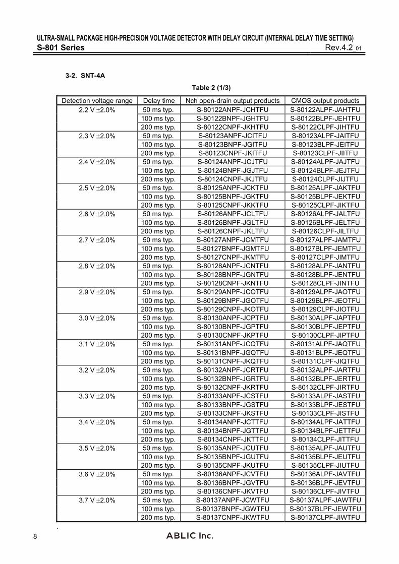
3-2. SNT-4A
Table 2 (1/3)
Detection voltage range Delay time Nch open-drain output products CMOS output products2.2 V 2.0% 50 ms typ. S-80122ANPF-JCHTFU S-80122ALPF-JAHTFU
100 ms typ. S-80122BNPF-JGHTFU S-80122BLPF-JEHTFU 200 ms typ. S-80122CNPF-JKHTFU S-80122CLPF-JIHTFU
2.3 V 2.0% 50 ms typ. S-80123ANPF-JCITFU S-80123ALPF-JAITFU 100 ms typ. S-80123BNPF-JGITFU S-80123BLPF-JEITFU 200 ms typ. S-80123CNPF-JKITFU S-80123CLPF-JIITFU
2.4 V 2.0% 50 ms typ. S-80124ANPF-JCJTFU S-80124ALPF-JAJTFU 100 ms typ. S-80124BNPF-JGJTFU S-80124BLPF-JEJTFU 200 ms typ. S-80124CNPF-JKJTFU S-80124CLPF-JIJTFU
2.5 V 2.0% 50 ms typ. S-80125ANPF-JCKTFU S-80125ALPF-JAKTFU 100 ms typ. S-80125BNPF-JGKTFU S-80125BLPF-JEKTFU 200 ms typ. S-80125CNPF-JKKTFU S-80125CLPF-JIKTFU
2.6 V 2.0% 50 ms typ. S-80126ANPF-JCLTFU S-80126ALPF-JALTFU 100 ms typ. S-80126BNPF-JGLTFU S-80126BLPF-JELTFU 200 ms typ. S-80126CNPF-JKLTFU S-80126CLPF-JILTFU
2.7 V 2.0% 50 ms typ. S-80127ANPF-JCMTFU S-80127ALPF-JAMTFU 100 ms typ. S-80127BNPF-JGMTFU S-80127BLPF-JEMTFU 200 ms typ. S-80127CNPF-JKMTFU S-80127CLPF-JIMTFU
2.8 V 2.0% 50 ms typ. S-80128ANPF-JCNTFU S-80128ALPF-JANTFU 100 ms typ. S-80128BNPF-JGNTFU S-80128BLPF-JENTFU 200 ms typ. S-80128CNPF-JKNTFU S-80128CLPF-JINTFU
2.9 V 2.0% 50 ms typ. S-80129ANPF-JCOTFU S-80129ALPF-JAOTFU 100 ms typ. S-80129BNPF-JGOTFU S-80129BLPF-JEOTFU 200 ms typ. S-80129CNPF-JKOTFU S-80129CLPF-JIOTFU
3.0 V 2.0% 50 ms typ. S-80130ANPF-JCPTFU S-80130ALPF-JAPTFU 100 ms typ. S-80130BNPF-JGPTFU S-80130BLPF-JEPTFU 200 ms typ. S-80130CNPF-JKPTFU S-80130CLPF-JIPTFU
3.1 V 2.0% 50 ms typ. S-80131ANPF-JCQTFU S-80131ALPF-JAQTFU 100 ms typ. S-80131BNPF-JGQTFU S-80131BLPF-JEQTFU 200 ms typ. S-80131CNPF-JKQTFU S-80131CLPF-JIQTFU
3.2 V 2.0% 50 ms typ. S-80132ANPF-JCRTFU S-80132ALPF-JARTFU 100 ms typ. S-80132BNPF-JGRTFU S-80132BLPF-JERTFU 200 ms typ. S-80132CNPF-JKRTFU S-80132CLPF-JIRTFU
3.3 V 2.0% 50 ms typ. S-80133ANPF-JCSTFU S-80133ALPF-JASTFU 100 ms typ. S-80133BNPF-JGSTFU S-80133BLPF-JESTFU 200 ms typ. S-80133CNPF-JKSTFU S-80133CLPF-JISTFU
3.4 V 2.0% 50 ms typ. S-80134ANPF-JCTTFU S-80134ALPF-JATTFU 100 ms typ. S-80134BNPF-JGTTFU S-80134BLPF-JETTFU 200 ms typ. S-80134CNPF-JKTTFU S-80134CLPF-JITTFU
3.5 V 2.0% 50 ms typ. S-80135ANPF-JCUTFU S-80135ALPF-JAUTFU 100 ms typ. S-80135BNPF-JGUTFU S-80135BLPF-JEUTFU 200 ms typ. S-80135CNPF-JKUTFU S-80135CLPF-JIUTFU
3.6 V 2.0% 50 ms typ. S-80136ANPF-JCVTFU S-80136ALPF-JAVTFU 100 ms typ. S-80136BNPF-JGVTFU S-80136BLPF-JEVTFU 200 ms typ. S-80136CNPF-JKVTFU S-80136CLPF-JIVTFU
3.7 V 2.0% 50 ms typ. S-80137ANPF-JCWTFU S-80137ALPF-JAWTFU 100 ms typ. S-80137BNPF-JGWTFU S-80137BLPF-JEWTFU 200 ms typ. S-80137CNPF-JKWTFU S-80137CLPF-JIWTFU
.
ULTRA-SMALL PACKAGE HIGH-PRECISION VOLTAGE DETECTOR WITH DELAY CIRCUIT (INTERNAL DELAY TIME SETTING)Rev.4.2_01 S-801 Series
9
Table 2 (2/3)
Detection voltage range Delay time Nch open-drain output products CMOS output products3.8 V 2.0% 50 ms typ. S-80138ANPF-JCXTFU S-80138ALPF-JAXTFU
100 ms typ. S-80138BNPF-JGXTFU S-80138BLPF-JEXTFU 200 ms typ. S-80138CNPF-JKXTFU S-80138CLPF-JIXTFU
3.9 V 2.0% 50 ms typ. S-80139ANPF-JCYTFU S-80139ALPF-JAYTFU 100 ms typ. S-80139BNPF-JGYTFU S-80139BLPF-JEYTFU 200 ms typ. S-80139CNPF-JKYTFU S-80139CLPF-JIYTFU
4.0 V 2.0% 50 ms typ. S-80140ANPF-JCZTFU S-80140ALPF-JAZTFU 100 ms typ. S-80140BNPF-JGZTFU S-80140BLPF-JEZTFU 200 ms typ. S-80140CNPF-JKZTFU S-80140CLPF-JIZTFU
4.1 V 2.0% 50 ms typ. S-80141ANPF-JC2TFU S-80141ALPF-JA2TFU 100 ms typ. S-80141BNPF-JG2TFU S-80141BLPF-JE2TFU 200 ms typ. S-80141CNPF-JK2TFU S-80141CLPF-JI2TFU
4.2 V 2.0% 50 ms typ. S-80142ANPF-JC3TFU S-80142ALPF-JA3TFU 100 ms typ. S-80142BNPF-JG3TFU S-80142BLPF-JE3TFU 200 ms typ. S-80142CNPF-JK3TFU S-80142CLPF-JI3TFU
4.3 V 2.0% 50 ms typ. S-80143ANPF-JC4TFU S-80143ALPF-JA4TFU 100 ms typ. S-80143BNPF-JG4TFU S-80143BLPF-JE4TFU 200 ms typ. S-80143CNPF-JK4TFU S-80143CLPF-JI4TFU
4.4 V 2.0% 50 ms typ. S-80144ANPF-JC5TFU S-80144ALPF-JA5TFU 100 ms typ. S-80144BNPF-JG5TFU S-80144BLPF-JE5TFU 200 ms typ. S-80144CNPF-JK5TFU S-80144CLPF-JI5TFU
4.5 V 2.0% 50 ms typ. S-80145ANPF-JC6TFU S-80145ALPF-JA6TFU 100 ms typ. S-80145BNPF-JG6TFU S-80145BLPF-JE6TFU 200 ms typ. S-80145CNPF-JK6TFU S-80145CLPF-JI6TFU
4.6 V 2.0% 50 ms typ. S-80146ANPF-JC7TFU S-80146ALPF-JA7TFU 100 ms typ. S-80146BNPF-JG7TFU S-80146BLPF-JE7TFU 200 ms typ. S-80146CNPF-JK7TFU S-80146CLPF-JI7TFU
4.7 V 2.0% 50 ms typ. S-80147ANPF-JC8TFU S-80147ALPF-JA8TFU 100 ms typ. S-80147BNPF-JG8TFU S-80147BLPF-JE8TFU 200 ms typ. S-80147CNPF-JK8TFU S-80147CLPF-JI8TFU
4.8 V 2.0% 50 ms typ. S-80148ANPF-JC9TFU S-80148ALPF-JA9TFU 100 ms typ. S-80148BNPF-JG9TFU S-80148BLPF-JE9TFU 200 ms typ. S-80148CNPF-JK9TFU S-80148CLPF-JI9TFU
4.9 V 2.0% 50 ms typ. S-80149ANPF-JDATFU S-80149ALPF-JBATFU 100 ms typ. S-80149BNPF-JHATFU S-80149BLPF-JFATFU 200 ms typ. S-80149CNPF-JLATFU S-80149CLPF-JJATFU
5.0 V 2.0% 50 ms typ. S-80150ANPF-JDBTFU S-80150ALPF-JBBTFU 100 ms typ. S-80150BNPF-JHBTFU S-80150BLPF-JFBTFU 200 ms typ. S-80150CNPF-JLBTFU S-80150CLPF-JJBTFU
5.1 V 2.0% 50 ms typ. S-80151ANPF-JDCTFU S-80151ALPF-JBCTFU 100 ms typ. S-80151BNPF-JHCTFU S-80151BLPF-JFCTFU 200 ms typ. S-80151CNPF-JLCTFU S-80151CLPF-JJCTFU
5.2 V 2.0% 50 ms typ. S-80152ANPF-JDDTFU S-80152ALPF-JBDTFU 100 ms typ. S-80152BNPF-JHDTFU S-80152BLPF-JFDTFU 200 ms typ. S-80152CNPF-JLDTFU S-80152CLPF-JJDTFU
5.3 V 2.0% 50 ms typ. S-80153ANPF-JDETFU S-80153ALPF-JBETFU 100 ms typ. S-80153BNPF-JHETFU S-80153BLPF-JFETFU 200 ms typ. S-80153CNPF-JLETFU S-80153CLPF-JJETFU
ULTRA-SMALL PACKAGE HIGH-PRECISION VOLTAGE DETECTOR WITH DELAY CIRCUIT (INTERNAL DELAY TIME SETTING) S-801 Series Rev.4.2_01
10
Table 2 (3/3)
Detection voltage range Delay time Nch open-drain output products CMOS output products5.4 V 2.0% 50 ms typ. S-80154ANPF-JDFTFU S-80154ALPF-JBFTFU
100 ms typ. S-80154BNPF-JHFTFU S-80154BLPF-JFFTFU 200 ms typ. S-80154CNPF-JLFTFU S-80154CLPF-JJFTFU
5.5 V 2.0% 50 ms typ. S-80155ANPF-JDGTFU S-80155ALPF-JBGTFU 100 ms typ. S-80155BNPF-JHGTFU S-80155BLPF-JFUTFU 200 ms typ. S-80155CNPF-JLGTFU S-80155CLPF-JJGTFU
5.6 V 2.0% 50 ms typ. S-80156ANPF-JDHTFU S-80156ALPF-JBHTFU 100 ms typ. S-80156BNPF-JHHTFU S-80156BLPF-JFHTFU 200 ms typ. S-80156CNPF-JLHTFU S-80156CLPF-JJHTFU
5.7 V 2.0% 50 ms typ. S-80157ANPF-JDITFU S-80157ALPF-JBITFU 100 ms typ. S-80157BNPF-JHITFU S-80157BLPF-JFITFU 200 ms typ. S-80157CNPF-JLITFU S-80157CLPF-JJITFU
5.8 V 2.0% 50 ms typ. S-80158ANPF-JDJTFU S-80158ALPF-JBJTFU 100 ms typ. S-80158BNPF-JHJTFU S-80158BLPF-JFJTFU 200 ms typ. S-80158CNPF-JLJTFU S-80158CLPF-JJJTFU
5.9 V 2.0% 50 ms typ. S-80159ANPF-JDKTFU S-80159ALPF-JBKTFU 100 ms typ. S-80159BNPF-JHKTFU S-80159BLPF-JFKTFU 200 ms typ. S-80159CNPF-JLKTFU S-80159CLPF-JJKTFU
6.0 V 2.0% 50 ms typ. S-80160ANPF-JDLTFU S-80160ALPF-JBLTFU 100 ms typ. S-80160BNPF-JHLTFU S-80160BLPF-JFLTFU 200 ms typ. S-80160CNPF-JLLTFU S-80160CLPF-JJLTFU
ULTRA-SMALL PACKAGE HIGH-PRECISION VOLTAGE DETECTOR WITH DELAY CIRCUIT (INTERNAL DELAY TIME SETTING)Rev.4.2_01 S-801 Series
11
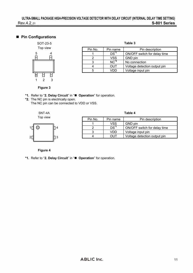
Pin Configurations
SOT-23-5 Top view
5 4
3 2 1
Table 3
Pin No. Pin name Pin description 1 DS*1 ON/OFF switch for delay time 2 VSS GND pin 3 NC*2 No connection 4 OUT Voltage detection output pin 5 VDD Voltage input pin
Figure 3
*1. Refer to “2. Delay Circuit” in “ Operation” for operation. *2. The NC pin is electrically open.
The NC pin can be connected to VDD or VSS.
SNT-4A
Top view
1 4
2 3
Table 4
Pin No. Pin name Pin description 1 VSS GND pin 2 DS*1 ON/OFF switch for delay time 3 VDD Voltage input pin 4 OUT Voltage detection output pin
Figure 4
*1. Refer to “2. Delay Circuit” in “ Operation” for operation.
ULTRA-SMALL PACKAGE HIGH-PRECISION VOLTAGE DETECTOR WITH DELAY CIRCUIT (INTERNAL DELAY TIME SETTING) S-801 Series Rev.4.2_01
12
Absolute Maximum Ratings
Table 5 (Ta25C unless otherwise specified)
Item Symbol Absolute maximum ratings Unit Power supply voltage VDDVSS 12 V Output voltage Nch open-drain output products VOUT VSS0.3 to VSS12 CMOS output products VSS0.3 to VDD+0.3 Output current IOUT 50 mA Power dissipation
SOT-23-5 PD 250 (When not mounted on board) mW 600*1 SNT-4A 140 (When not mounted on board) 300*1
Operating ambient temperature Topr 40 to +85 C Storage temperature Tstg 40 to +125
*1. When mounted on board [Mounted board] (1) Board size: 114.3 mm 76.2 mm t1.6 mm (2) Board name: JEDEC STANDARD51-7 Caution The absolute maximum ratings are rated values exceeding which the product could suffer
physical damage. These values must therefore not be exceeded under any conditions.
0 50 100 150
600
400
0
Po
we
r D
issi
patio
n (
PD)
[mW
]
Ambient Temperature (Ta) [C]
200
100
300
500
700
SNT-4A
SOT-23-5
Figure 5 Power Dissipation of Package (When Mounted on Board)
ULTRA-SMALL PACKAGE HIGH-PRECISION VOLTAGE DETECTOR WITH DELAY CIRCUIT (INTERNAL DELAY TIME SETTING)Rev.4.2_01 S-801 Series
13
Electrical Characteristics
Table 6 (Ta25 C Unless otherwise specified)
Item Symbol Condition Min. Typ. Max. UnitTest
circuit
Detection voltage*1 VDET — VDET(S)
0.98VDET(S)
VDET(S)
1.02 V 1
Hysteresis width VHYS — 30 60 100 mV Current consumption
ISS VDD3.5 V S-80122 to 26 — 1.3 3.3 A VDD4.5 V S-80127 to 39 — 1.5 3.5
VDD6.5 V S-80140 to 60 — 1.8 4.0 Operating voltage VDD — 0.95 — 10.0 V
Output current IOUT Output transistor, Nch, VOUT0.5 V
VDD1.2 V S-80122 to 60
0.75 1.5 — mA 2
VDD2.4 V S-80127 to 60
3.0 6.0 —
Only for CMOS output products, Output transistor, Pch, VDD–VOUT0.5 V
VDD4.8 V S-80122 to 39
1.0 2.0 —
VDD6.0 V S-80140 to 54
1.25 2.5 —
VDD8.4 V S-80155 to 60
1.5 3.0 —
Leakage current ILEAK Only for Nch open-drain output products, Output transistor, Nch, VDD10.0 V, VOUT10.0 V
— — 0.1 A
Detection voltage temperature coefficient *2
DET
DET
VTa
V
Ta40 °C to 85 °C — 120 360
ppm/°C
1
Delay time 1 tD1 VDDVDET1 V, DS pin Low S-801xxAx 32.5 50 72.5 ms S-801xxBx 65 100 145 S-801xxCx 130 200 290 Delay time 2 tD2 VDDVDET+1 V, DS pin High 110 220 330 s 3 Input voltage VSH DS pin, VDD6.0 V 1.0 — — V 4 VSL DS pin, VDD6.0 V — — 0.3
*1. VDET: Actual detection voltage value, VDET(S): Specified detection voltage value (The center value of the detection voltage range in Table 1 to 2.)
*2. Temperature change ratio for the detection voltage [mV/C] is calculated using the following equation.
1000Cppm/ VTa∆
V∆V Typ.VCmV/
Ta∆
V∆
DET
DET DET(S)
DET
3*2**1
*1. Temperature change ratio of the detection voltage *2. Specified detection voltage value *3. Detection voltage temperature coefficient
ULTRA-SMALL PACKAGE HIGH-PRECISION VOLTAGE DETECTOR WITH DELAY CIRCUIT (INTERNAL DELAY TIME SETTING) S-801 Series Rev.4.2_01
14
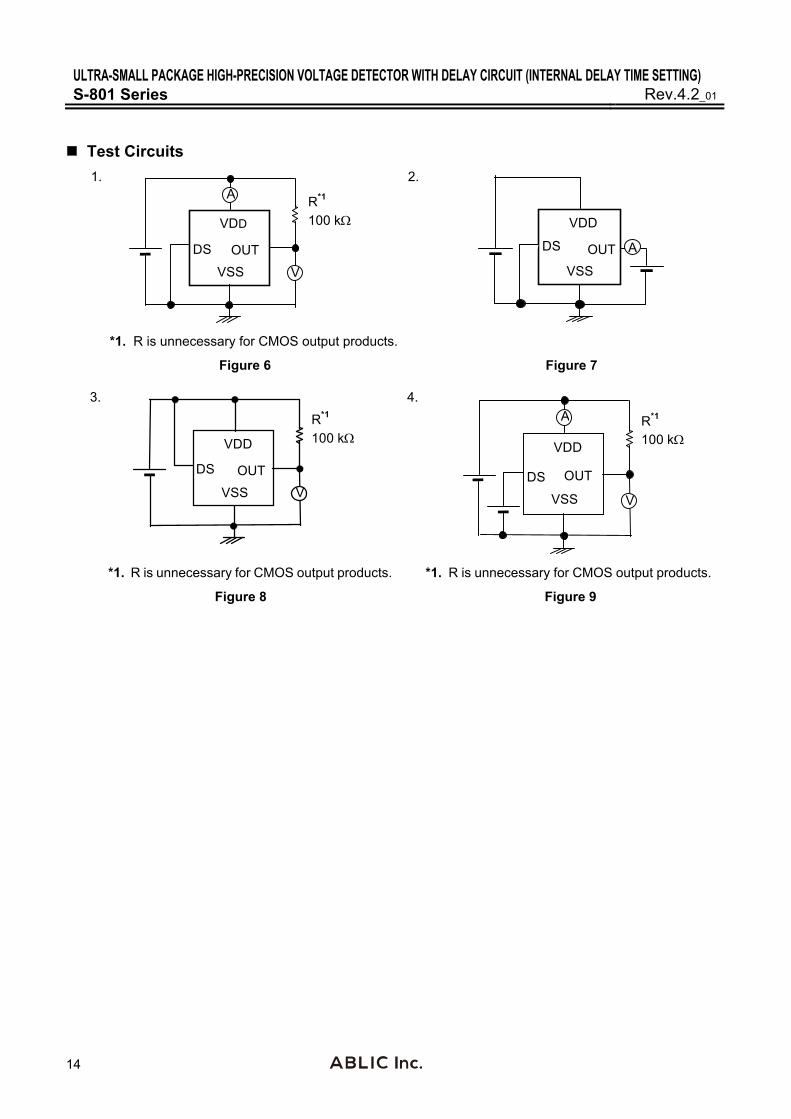
Test Circuits
1.
DS
VDD
OUT
VSS
R*1
100 k
A
V
2.
DS
VDD
OUT
VSS
A
*1. R is unnecessary for CMOS output products.
Figure 6 Figure 7 3.
DS
VDD
OUT
VSS
R*1
100 k
V
4.
DS
VDD
OUT
VSS
R*1 100 k
A
V
*1. R is unnecessary for CMOS output products. *1. R is unnecessary for CMOS output products.
Figure 8 Figure 9
ULTRA-SMALL PACKAGE HIGH-PRECISION VOLTAGE DETECTOR WITH DELAY CIRCUIT (INTERNAL DELAY TIME SETTING)Rev.4.2_01 S-801 Series
15
Operation
1. Basic Operation: CMOS Output (Active Low)
1-1. When the power supply voltage (VDD) is higher than the release voltage (VDET), the Nch transistor is OFF and the Pch transistor is ON to provide VDD (high) at the output. Since the
Nch transistor N1 in Figure 10 is OFF, the comparator input voltage is CBA
DDCB
RRR
V)RR(
.
1-2. When the VDD goes below VDET, the output provides the VDD level, as long as VDD remains above the detection voltage (–VDET). When the VDD falls below –VDET (point A in Figure 11), the Nch transistor becomes ON, the Pch transistor becomes OFF, and the VSS level appears at the output. At this time the Nch transistor N1 in Figure 10 becomes ON, the comparator
input voltage is changed to BA
DDB
RR
VR
.
1-3. When the VDD falls below the minimum operating voltage, the output becomes undefined, or goes to VDD when the output is pulled up to VDD.
1-4. The VSS level appears when VDD rises above the minimum operating voltage. The VSS level still appears even when VDD surpasses the –VDET, as long as it does not exceed the release voltage VDET.
1-5. When VDD rises above VDET (point B in Figure 11), the Nch transistor becomes OFF and the Pch transistor becomes ON to provide VDD at the output. The VDD at the OUT pin is delayed for tD due to the delay circuit.
*1
DS
*1
RC
RB
Pch
NchVREF
VDD
RA
N1
VSS
OUT Delay circuit
*1. Paracitic diode
Figure 10 Operation 1
ULTRA-SMALL PACKAGE HIGH-PRECISION VOLTAGE DETECTOR WITH DELAY CIRCUIT (INTERNAL DELAY TIME SETTING) S-801 Series Rev.4.2_01
16
AB
VDD
tD
VSS Minimum operating voltage
Output from OUT pin
VDD
VSS
(1) (2) (3) (5)(4)
Hysterisis width (VHYS)Release voltage (VDET) Detection voltage (VDET)
Figure 11 Operation 2 2. Delay Circuit
2-1. Delay Time
The delay circuit delays the output signal from the time at which the power voltage (VDD) exceeds the release voltage (VDET) when VDD is turned on. The output signal is not delayed when the VDD goes below the detection voltage (–VDET). (Refer to Figure 11.) The delay time (tD) is a fixed value that is determined by a built-in oscillation circuit and counter.
2-2. DS Pin (ON/OFF Switch Pin for Delay Time)
The DS pin should be connected to Low or High. When the DS pin is High, the output delay time becomes short since the output signal is taken from the middle of counter circuit (Refer to Figure 16).
3. Other Characteristics
3-1. Temperature Characteristics of Detection Voltage
The shaded area in Figure 12 shows the temperature characteristics of the detection voltage.
–40 25
0.792 mV/C
2.200
85 Ta [C]
–0.792 mV/C
–VDET [V]
Figure 12 Temperature Characteristics of Detection Voltage (Example for S-80122xxxx)
ULTRA-SMALL PACKAGE HIGH-PRECISION VOLTAGE DETECTOR WITH DELAY CIRCUIT (INTERNAL DELAY TIME SETTING)Rev.4.2_01 S-801 Series
17
3-2. Temperature Characteristics of Release Voltage
The temperature coefficient Ta
VDET
of the release voltage is calculated by the temperature
coefficient Ta
VDET
for the detection voltage as follows:
Ta
V
V
V
Ta
V DET
DET
DETDET
The temperature coefficients for the release voltage and the detection voltage have the same sign consequently.
3-3. Temperature Characteristics of Hysteresis Voltage
The temperature characteristics for the hysteresis voltage is expressed as Ta
V
Ta
V DETDET
and
is calculated as follows:
Ta
V
V
V
Ta
V
Ta
V DET
DET
HYSDETDET
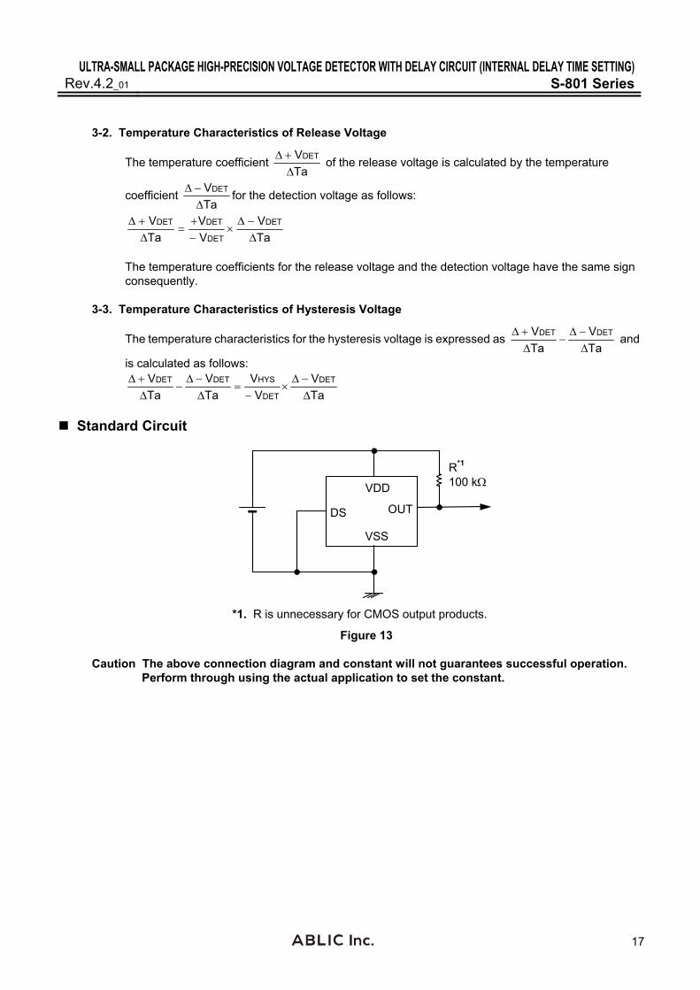
Standard Circuit
DS
VDD
OUT
VSS
R*1
100 k
*1. R is unnecessary for CMOS output products.
Figure 13 Caution The above connection diagram and constant will not guarantees successful operation.
Perform through using the actual application to set the constant.
ULTRA-SMALL PACKAGE HIGH-PRECISION VOLTAGE DETECTOR WITH DELAY CIRCUIT (INTERNAL DELAY TIME SETTING) S-801 Series Rev.4.2_01
18
Technical Terms
1. Detection Voltage (–VDET), Release Voltage (VDET)
The detection voltage (–VDET) is a voltage at which the output turns to low. The detection voltage varies slightly among products of the same specification. The variation of detection voltage between the specified minimum (–VDET) Min. and the maximum (–VDET) Max. is called the detection voltage range (Refer to Figure 14). e.g. For the S-80122AN, the detection voltage lies in the range of 2.156 (–VDET) 2.244.
This means that some S-80122ANs have 2.156 V for –VDET and some have 2.244 V. The release voltage (VDET) is a voltage at which the output turns to high. The release voltage varies slightly among products of the same specification. The variation of release voltages between the specified minimum (VDET) Min. and the maximum (VDET) Max. is called the release voltage range (Refer to Figure 15). e.g. For the S-80122AN, the release voltage lies in the range of 2.186 (VDET) 2.344.
This means that some S-80122ANs have 2.186 V for VDET and some have 2.344 V.
Detection voltage
Detection voltage range
VDD
(VDET) Min.
(VDET) Max.
OUT
Delay time
Release voltage
Release voltage range
VDD
(VDET) Min.
(VDET) Max.
OUT
Figure 14 Detection Voltage Figure 15 Release Voltage Remark Although the detection voltage and release voltage overlap in the range of 2.186 V to 2.244 V,
VDET is always larger than –VDET.
ULTRA-SMALL PACKAGE HIGH-PRECISION VOLTAGE DETECTOR WITH DELAY CIRCUIT (INTERNAL DELAY TIME SETTING)Rev.4.2_01 S-801 Series
19
2. Hysteresis Width (VHYS)
Hysteresis width is the voltage difference between the detection voltage and the release voltage (The voltage at point BThe voltage at point AVHYS in Figure 11). The existence of the hysteresis width prevents malfunction caused by noise on input signal.
3. Delay Time (tD)
Delay time is a time internally measured from the instant at which input voltage to the VDD pin exceeds the release voltage (VDET) to the point at which the output of the OUT pin inverts. The delay time is fixed in each series distinguished by A, B and C.
S-801xxAx series: typ. 50 ms S-801xxBx series: typ. 100 ms S-801xxCx series: typ. 200 ms
The output of the OUT pin can be inverted in a short delay time (tD2) by setting the DS pin High (Refer to Figure 16).
tD2
tD1
VDD
at DS”H” OUT
V
VDET
Figure 16 4. Through-type Current
The through-type current refers to the current that flows instantaneously at the time of detection and release of a voltage detector. The through-type current flows at a frequency of 20 kHz during release delay time since the internal logic circuit operates.
ULTRA-SMALL PACKAGE HIGH-PRECISION VOLTAGE DETECTOR WITH DELAY CIRCUIT (INTERNAL DELAY TIME SETTING) S-801 Series Rev.4.2_01
20
5. Oscillation
In applications where a resistor is connected to the voltage detector input (Figure 17), taking a CMOS active low products for example, the through-type current which is generated when the output goes from low to high (release) causes a voltage drop equal to [through-type current] [input resistance] across the resistor. When the input voltage drops below the detection voltage (–VDET) as a result, the output voltage goes to low level. In this state, the through-type current stops and its resultant voltage drop disappears, and the output goes from low to high. The through-type current is again generated, a voltage drop appears, and repeating the process finally induces oscillation.
OUT
VSS
VDD
RB
RA
VIN S-801
Figure 17 Example for Bad Implementation of Input Voltage Divider Precautions
In the S-801 series products, the through-type current flows at a frequency of 20 kHz approximately during the delay time since the internal oscillator circuit and counter timer operate at voltage release. High impedance in the input may cause oscillation by the through-type current. When the input impedance is high, insert a capacitor between VDD pin and VSS pin to prevent oscillation.
Do not apply an electrostatic discharge to this IC that exceeds the performance ratings of the built-in electrostatic protection circuit.
In CMOS output products of the S-801 Series, the through-type current flows at detection and release. If the impedance is high, oscillation may occur due to the voltage drop by the through-type current during releasing.
When designing for mass production using an application circuit described herein, the product deviation and temperature characteristics should be taken into consideration. ABLIC Inc. shall not bear any responsibility for the patents on the circuits described herein.
ABLIC Inc. claims no responsibility for any and all disputes arising out of or in connection with any infringement of the products including this IC upon patents owned a third party.
ULTRA-SMALL PACKAGE HIGH-PRECISION VOLTAGE DETECTOR WITH DELAY CIRCUIT (INTERNAL DELAY TIME SETTING)Rev.4.2_01 S-801 Series
21
Typical Characteristics (Typical Data)
1. Detection Voltage (VDET) - Temperature (Ta) S-80122AL S-80160AL
2.1
2.2
2.3
2.4
40 20 0 20 40 60 80 100Ta [°C]
VD
ET [V
] VDET ()
VDET ()
5.8
6.0
6.2
6.4
40 20 0 20 40 60 80 100Ta [°C)]
VD
ET [V
]
VDET ()
VDET ()
2. Hysteresis Voltage Width (VHYS) - Temperature (Ta) S-80122AL S-80160AL
30
40
50
60
70
80
90
100
40 20 0 20 40 60 80 100Ta [°C]
VH
YS [m
V]
30
40
50
60
70
80
90
100
40 20 0 20 40 60 80 100Ta [°C]
VH
YS [m
V]
3. Current Consumption (ISS) - Input Voltage (VDD) (a) S-80122AL (b) S-80129AL
0.0
0.5
1.0
1.5
2.0
2.5
3.0
3.5
0 2 4 6 8 10VDD [V]
I SS [
A]
Ta25°C
2.9 A
0.0
0.5
1.0
1.5
2.0
2.5
3.0
3.5
0 2 4 6 8 10VDD [V]
I SS [
A]
Ta25°C
3.3 A
(c) S-80130AL (d) S-80160AL
0.0
0.5
1.0
1.5
2.0
2.5
3.0
3.5
0 2 4 6 8 10VDD [V]
I SS [
A]
Ta25°C5.0 A
0.0
0.5
1.0
1.5
2.0
2.5
3.0
3.5
0 2 4 6 8 10VDD [V]
I SS [
A]
Ta25°C20 A
ULTRA-SMALL PACKAGE HIGH-PRECISION VOLTAGE DETECTOR WITH DELAY CIRCUIT (INTERNAL DELAY TIME SETTING) S-801 Series Rev.4.2_01
22
4. Current Consumption (ISS) - Temperature (Ta) (a) S-80122AL (b) S-80129AL
0.0
1.0
2.0
3.0
4.0
5.0
40 20 0 20 40 60 80 100Ta [°C]
I SS [
A]
VDD3.5 V
0.0
1.0
2.0
3.0
4.0
5.0
40 20 0 20 40 60 80 100Ta [°C]
I SS [
A]
VDD4.5 V
(c) S-80130AL (d) S-80160AL
0.0
1.0
2.0
3.0
4.0
5.0
40 20 0 20 40 60 80 100Ta [°C]
I SS [
A]
VDD4.5 V
0.0
1.0
2.0
3.0
4.0
5.0
40 20 0 20 40 60 80 100Ta [°C]
I SS [
A]
VDD6.5 V
5. Nch Transistor Output Current (IOUT) -VOUT 6. Pch Transistor Output Current (IOUT) - (VDD-VOUT) S-80160AL S-80122AL
0
10
20
30
40
50
60
70
0 2 4 6 8 10VOUT [V]
I OU
T [m
A]
Ta25°C
2 V
2.4 V
4 V
5.5 V VDD1 V, 1.2 V
0
10
20
30
40
0 2 4 6 8 10VDD-VOUT [V]
I OU
T [m
A]
Ta25°C
VDD4 V 4.8 V
6 V
6.5 V
10 V
8 V
7. Nch Transistor Output Current (IOUT) - Input Voltage (VDD)
8. Pch transistor Output Current (IOUT) - Input Voltage (VDD)
S-80160AL S-80122AL
0
5
10
15
20
25
0 2 4 6 8 10VDD [V]
I OU
T [m
A]
VDS0.5 V
Ta 40°C
85°C
25°C
0
1
2
3
4
5
0 2 4 6 8 10VDD [V]
I OU
T [m
A]
VDS0.5 V
Ta 40°C
85°C
25°C
ULTRA-SMALL PACKAGE HIGH-PRECISION VOLTAGE DETECTOR WITH DELAY CIRCUIT (INTERNAL DELAY TIME SETTING)Rev.4.2_01 S-801 Series
23
9. Minimum Operating Voltage - Input Voltage (VDD) S-80122AN
0
0.1
0.2
0.3
0.4
0.5
0.6
0 0.5 1 1.5VDD [V]
VO
UT [V
]
Pull-up, VDD:100 k
85°C
25°C
Ta 40°C
10. Threshold Voltage of DS Pin - Temperature (Ta) 11. Threshold Voltage of DS Pin - Input Voltage (VDD) S-80122AL S-80122AL
0
0.2
0.4
0.6
0.8
1
40 20 0 20 40 60 80 100 Ta [°C]
Thr
esho
ld [
V]
VDD6.0 V
0
0.2
0.4
0.6
0.8
1
0 2 4 6 8 10VDD [V]
Thr
esho
ld [V
] Ta 40°C
25°C
85°C
12. Delay Time 1 - Temperature (Ta) S-80122CL S-80160CL
0
50
100
150
200
250
300
40 20 0 20 40 60 80 100 Ta [°C]
Del
ay ti
me
[ms]
VDD3.2 V
0
50
100
150
200
250
300
40 20 0 20 40 60 80 100 Ta [°C]
Del
ay ti
me
[ms]
VDD7.0 V
13. Delay Time 1 - Input Voltage (VDD) S-80122CL
0
50
100
150
200
250
300
2 4 6 8 10 VDD [V]
Del
ay ti
me
[ms]
Ta25°C
ULTRA-SMALL PACKAGE HIGH-PRECISION VOLTAGE DETECTOR WITH DELAY CIRCUIT (INTERNAL DELAY TIME SETTING) S-801 Series Rev.4.2_01
24
14. Delay Time 2 - Temperature (Ta) S-80122AL S-80160AL
0
50
100
150
200
250
300
350
400
40 20 0 20 40 60 80 100 Ta [°C]
Del
ay ti
me
[ s]
VDD3.2 V
0
50
100
150
200
250
300
350
400
40 20 0 20 40 60 80 100 Ta [°C]
Del
ay
time
[ s]
VDD7.0 V
15. Delay Time 2 - Input Voltage (VDD) S-80122AN
0
50
100
150
200
250
300
350
400
2 4 6 8 10 VDD [V]
Del
ay ti
me
[ s]
Ta25°C
VDD90 %
VSS
VIH
VILtD
VIH10 V, VIL0.95 V
INPUT VOLTAGE
OUTPUT VOLTAGE
1s
VDD
OUT
VSS
DS*1
VDD
S-801 Series V
V
R*2 100 k
*1. Set to VDD or VSS. *2. R is not necessary for CMOS output products.
Figure 18 Measurment Condition for Delay Time Figure 19 Measurment Circuit for Delay Time Caution The above connection diagram will not guarantees successful operation. Perform through using
the actual application to set the constant.
ULTRA-SMALL PACKAGE HIGH-PRECISION VOLTAGE DETECTOR WITH DELAY CIRCUIT (INTERNAL DELAY TIME SETTING)Rev.4.2_01 S-801 Series
25
16. Response Time - Load Capacitor (COUT) S-80122AL S-80122AN
0.001
0.01
0.1
1
0.00001 0.0001 0.001 0.01 0.1COUT [F]
Re
spo
nse
time
[ms]
Ta25°C
tPLH (Delay time2)
tPHL
0.001
0.01
0.1
1
10
100
0.00001 0.0001 0.001 0.01 0.1COUT [F]
Re
spo
nse
tim
e [m
s]
Ta25°C
tPLH (Delay time2)
tPHL
S-80160AL S-80160AN
0.001
0.01
0.1
1
0.00001 0.0001 0.001 0.01 0.1COUT [F]
Res
pons
e tim
e [m
s]
Ta25°C
tPLH (Delay time2)
tPHL
0.001
0.01
0.1
1
10
100
0.00001 0.0001 0.001 0.01 0.1COUT [F]
Re
spo
nse
tim
e [m
s]
Ta25°C
tPLH (Delay time2)
tPHL
VDD 90 %
VDD 10 %
VIH
INPUT VOLTAGE
OUTPUT VOLTAGE
VIL
VDD
tPHL tPLH
VIH=10 V, VIL=0.95 V
1s 1s
VDD OUT
DS
VSS
VDD
S-801 Series
V
R*1
100 k
V
*1. R is not necessary for CMOS output products.
Figure 20 Measurment Condition for Response Time Figure 21 Measurment Circuit for Response Time Caution The above connection diagram will not guarantees successful operation. Perform through using
the actual application to set the constant.
ULTRA-SMALL PACKAGE HIGH-PRECISION VOLTAGE DETECTOR WITH DELAY CIRCUIT (INTERNAL DELAY TIME SETTING) S-801 Series Rev.4.2_01
26
Application Circuit Examples
Microcomputer Reset Circuits
If the power supply voltage to a microcomputer falls below the specified level, an unspecified operation may be performed or the contents of the memory register may be lost. When power supply voltage returns to normal, the microcomputer needs to be initialized before normal operations can be done. Reset circuits protect microcomputers in the event of current being momentarily switched off or lowered. Reset circuits shown in Figures 22 to 23 can be easily constructed with the help of the S-801 series that has low operating voltage, a high-precision detection voltage, hysteresis, and a built-in delay circuit.
VSS
VDD
Microcomputer S- 801xxAL
VSS
(Nch open-drain output products only.)
VDD1 VDD2
MicrocomputerS- 801xxAN
Figure 22 Ret Circuit (S-801xxAL) Figure 23 Reset Circuit (S-801xxAN) Caution The above connection diagram will not guarantees successful operation. Perform
through using the actual application to set the constant.
1. All the information described herein (product data, specifications, figures, tables, programs, algorithms and application circuit examples, etc.) is current as of publishing date of this document and is subject to change without notice.
2. The circuit examples and the usages described herein are for reference only, and do not guarantee the success of any specific mass-production design. ABLIC Inc. is not responsible for damages caused by the reasons other than the products described herein (hereinafter "the products") or infringement of third-party intellectual property right and any other right due to the use of the information described herein.
3. ABLIC Inc. is not responsible for damages caused by the incorrect information described herein.
4. Be careful to use the products within their specified ranges. Pay special attention to the absolute maximum ratings, operation voltage range and electrical characteristics, etc. ABLIC Inc. is not responsible for damages caused by failures and / or accidents, etc. that occur due to the use of the products outside their specified ranges.
5. When using the products, confirm their applications, and the laws and regulations of the region or country where they are used and verify suitability, safety and other factors for the intended use.
6. When exporting the products, comply with the Foreign Exchange and Foreign Trade Act and all other export-related laws, and follow the required procedures.
7. The products must not be used or provided (exported) for the purposes of the development of weapons of mass destruction or military use. ABLIC Inc. is not responsible for any provision (export) to those whose purpose is to develop, manufacture, use or store nuclear, biological or chemical weapons, missiles, or other military use.
8. The products are not designed to be used as part of any device or equipment that may affect the human body, human life, or assets (such as medical equipment, disaster prevention systems, security systems, combustion control systems, infrastructure control systems, vehicle equipment, traffic systems, in-vehicle equipment, aviation equipment, aerospace equipment, and nuclear-related equipment), excluding when specified for in-vehicle use or other uses. Do not apply the products to the above listed devices and equipments without prior written permission by ABLIC Inc. Especially, the products cannot be used for life support devices, devices implanted in the human body and devices that directly affect human life, etc. Prior consultation with our sales office is required when considering the above uses. ABLIC Inc. is not responsible for damages caused by unauthorized or unspecified use of our products.
9. Semiconductor products may fail or malfunction with some probability. The user of the products should therefore take responsibility to give thorough consideration to safety design including redundancy, fire spread prevention measures, and malfunction prevention to prevent accidents causing injury or death, fires and social damage, etc. that may ensue from the products' failure or malfunction. The entire system must be sufficiently evaluated and applied on customer's own responsibility.
10. The products are not designed to be radiation-proof. The necessary radiation measures should be taken in the product design by the customer depending on the intended use.
11. The products do not affect human health under normal use. However, they contain chemical substances and heavy metals and should therefore not be put in the mouth. The fracture surfaces of wafers and chips may be sharp. Be careful when handling these with the bare hands to prevent injuries, etc.
12. When disposing of the products, comply with the laws and ordinances of the country or region where they are used.
13. The information described herein contains copyright information and know-how of ABLIC Inc. The information described herein does not convey any license under any intellectual property rights or any other rights belonging to ABLIC Inc. or a third party. Reproduction or copying of the information from this document or any part of this document described herein for the purpose of disclosing it to a third-party without the express permission of ABLIC Inc. is strictly prohibited.
14. For more details on the information described herein, contact our sales office.