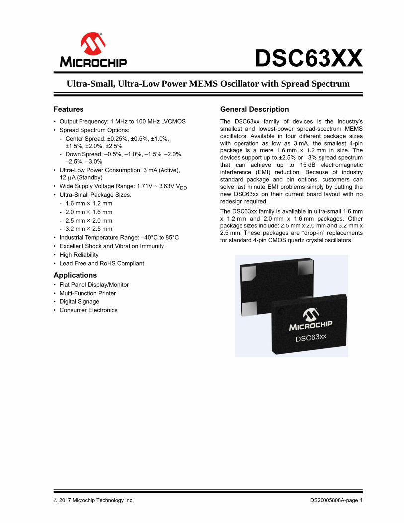
2017 Microchip Technology Inc. DS20005808A-page 1 DSC63XX Features • Output Frequency: 1 MHz to 100 MHz LVCMOS • Spread Spectrum Options: - Center Spread: ±0.25%, ±0.5%, ±1.0%, ±1.5%, ±2.0%, ±2.5% - Down Spread: –0.5%, –1.0%, –1.5%, –2.0%, –2.5%, –3.0% • Ultra-Low Power Consumption: 3 mA (Active), 12 A (Standby) • Wide Supply Voltage Range: 1.71V ~ 3.63V V DD • Ultra-Small Package Sizes: - 1.6 mm 1.2 mm - 2.0 mm 1.6 mm - 2.5 mm 2.0 mm - 3.2 mm 2.5 mm • Industrial Temperature Range: –40°C to 85°C • Excellent Shock and Vibration Immunity • High Reliability • Lead Free and RoHS Compliant Applications • Flat Panel Display/Monitor • Multi-Function Printer • Digital Signage • Consumer Electronics General Description The DSC63xx family of devices is the industry’s smallest and lowest-power spread-spectrum MEMS oscillators. Available in four different package sizes with operation as low as 3 mA, the smallest 4-pin package is a mere 1.6 mm x 1.2 mm in size. The devices support up to ±2.5% or –3% spread spectrum that can achieve up to 15 dB electromagnetic interference (EMI) reduction. Because of industry standard package and pin options, customers can solve last minute EMI problems simply by putting the new DSC63xx on their current board layout with no redesign required. The DSC63xx family is available in ultra-small 1.6 mm x 1.2 mm and 2.0 mm x 1.6 mm packages. Other package sizes include: 2.5 mm x 2.0 mm and 3.2 mm x 2.5 mm. These packages are “drop-in” replacements for standard 4-pin CMOS quartz crystal oscillators. Ultra-Small, Ultra-Low Power MEMS Oscillator with Spread Spectrum
Transcript
2017 Microchip Technology Inc. DS20005808A-page 1
DSC63XX
Features
• Output Frequency: 1 MHz to 100 MHz LVCMOS
• Spread Spectrum Options:
- Center Spread: ±0.25%, ±0.5%, ±1.0%, ±1.5%, ±2.0%, ±2.5%
- Down Spread: –0.5%, –1.0%, –1.5%, –2.0%, –2.5%, –3.0%
• Ultra-Low Power Consumption: 3 mA (Active), 12 A (Standby)
• Wide Supply Voltage Range: 1.71V ~ 3.63V VDD
• Ultra-Small Package Sizes:
- 1.6 mm 1.2 mm
- 2.0 mm 1.6 mm
- 2.5 mm 2.0 mm
- 3.2 mm 2.5 mm
• Industrial Temperature Range: –40°C to 85°C
• Excellent Shock and Vibration Immunity
• High Reliability
• Lead Free and RoHS Compliant
Applications• Flat Panel Display/Monitor
• Multi-Function Printer
• Digital Signage
• Consumer Electronics
General Description
The DSC63xx family of devices is the industry’ssmallest and lowest-power spread-spectrum MEMSoscillators. Available in four different package sizeswith operation as low as 3 mA, the smallest 4-pinpackage is a mere 1.6 mm x 1.2 mm in size. Thedevices support up to ±2.5% or –3% spread spectrumthat can achieve up to 15 dB electromagneticinterference (EMI) reduction. Because of industrystandard package and pin options, customers cansolve last minute EMI problems simply by putting thenew DSC63xx on their current board layout with noredesign required.
The DSC63xx family is available in ultra-small 1.6 mmx 1.2 mm and 2.0 mm x 1.6 mm packages. Otherpackage sizes include: 2.5 mm x 2.0 mm and 3.2 mm x2.5 mm. These packages are “drop-in” replacementsfor standard 4-pin CMOS quartz crystal oscillators.
Ultra-Small, Ultra-Low Power MEMS Oscillator with Spread Spectrum
DSC63XX
DS20005808A-page 2 2017 Microchip Technology Inc.
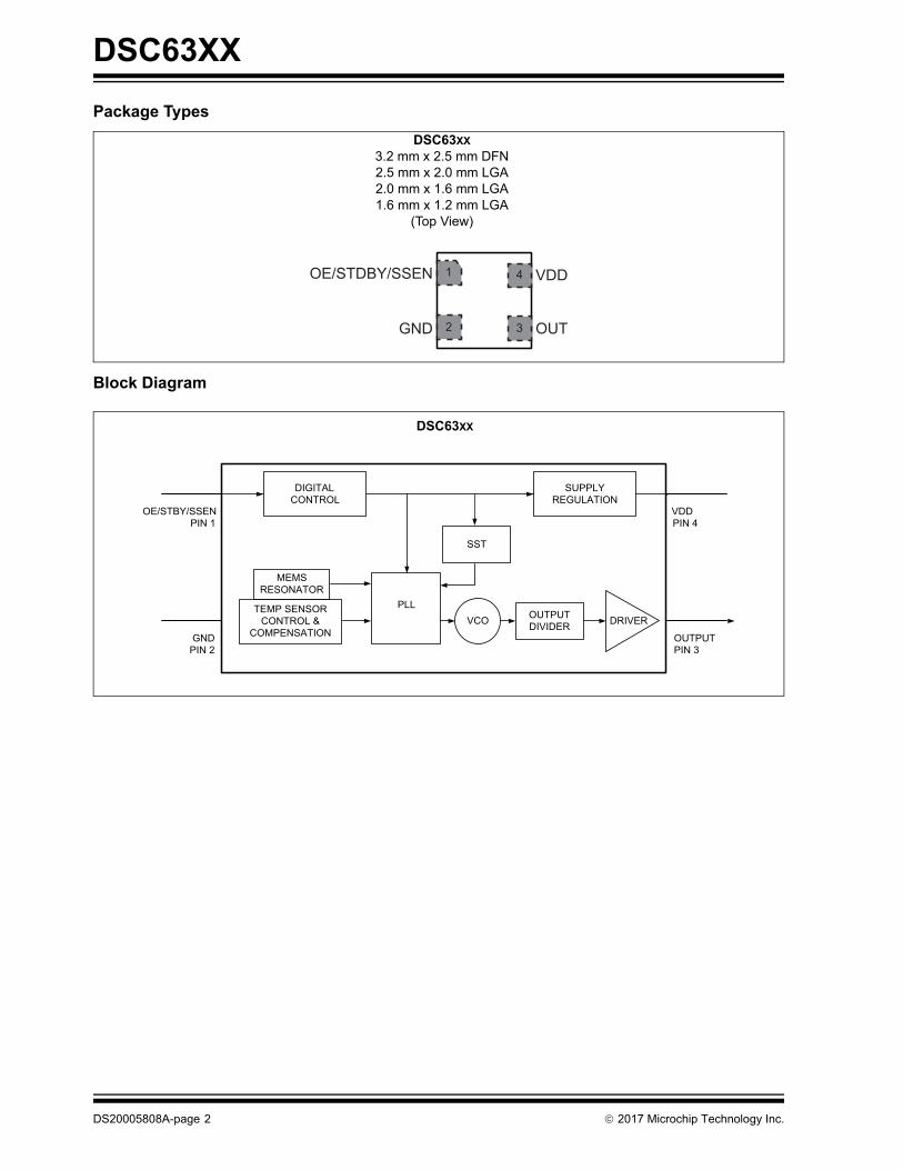
Package Types
Block Diagram
DSC63XX
3.2 mm x 2.5 mm DFN2.5 mm x 2.0 mm LGA2.0 mm x 1.6 mm LGA1.6 mm x 1.2 mm LGA
(Top View)
OE/STDBY/SSEN 4
GND
VDD
OUT32
1
DSC63XX
MEMSRESONATOR
TEMP SENSORCONTROL &
COMPENSATION
PLLVCO OUTPUT
DIVIDER DRIVER
SUPPLYREGULATION
PIN 1OE/STBY/SSEN
PIN 2GND
PIN 4VDD
PIN 3OUTPUT
DIGITALCONTROL
SST
2017 Microchip Technology Inc. DS20005808A-page 3
DSC63XX
1.0 ELECTRICAL CHARACTERISTICS
Absolute Maximum Ratings
Supply Voltage .......................................................................................................................................... –0.3V to +4.0VInput Voltage (VIN) ..............................................................................................................................–0.3V to VDD+0.3VESD Protection ............................................................................................................ 4 kV HBM, 400V MM, 2 kV CDM
DSC63XX ELECTRICAL CHARACTERISTICS
Electrical Characteristics: Unless otherwise indicated, VDD = 1.8V –5% to 3.3V +10%, TA = –40°C to 85°C.
Parameters Sym. Min. Typ. Max. Units Conditions
Supply Voltage, Note 1 VDD 1.71 — 3.63 V —
Power Supply Ramp tPU 0.1 — 100 ms Note 8
Active Supply Current IDD — 3.0 — mAFOUT = 27 MHz, VDD = 1.8V,
No Load
Standby Supply Current Note 2
ISTBY— 12 —
µAVDD = 1.8/2.5V
— 80 — VDD = 3.3V
Frequency Stability Note 3 ∆f — —±25±50
ppm All temp ranges
Aging ∆f— — ±5
ppm1st year @25°C
— — ±1 Per year after first year
Startup Time tSU — — 1.3 msFrom 90% VDD to valid clock
output, T = 25°C
Input Logic Levels Note 4VIH 0.7 x VDD — — V Input Logic High
VIL — — 0.3 x VDD V Input Logic Low
Output Disable Time Note 5
tDA — — 200+Period ns —
Output Enable Time Note 6
tEN — — 1 µs —
OE/STDBY/SSEN Pull-up Resistor Note 7
— — 300 — kΩ If configured
Output Logic Levels
VOH 0.8 x VDD — — V
Output Logic High, I = 3 mA, Std. Drive
Output Logic High, I = 6 mA, High Drive
VOL — — 0.2 x VDD V
Output Logic Low, I = –3 mA, Std. Drive
Output Logic Low, I = –6 mA, High Drive
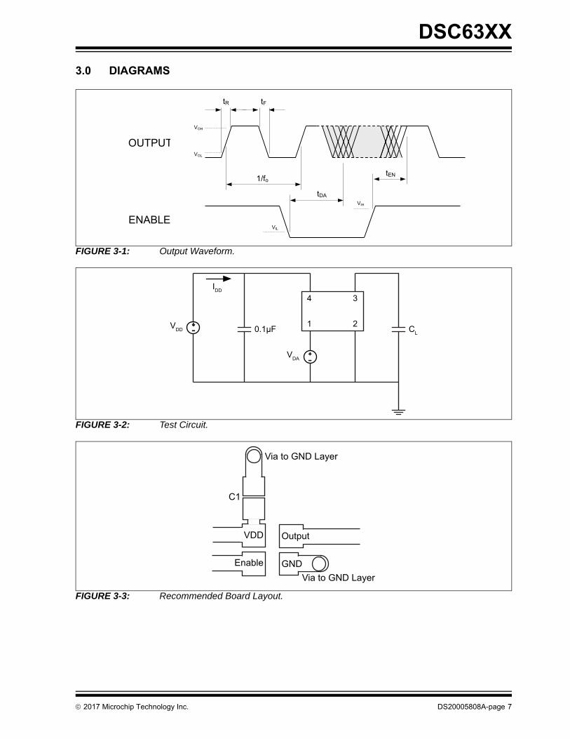
Note 1: Pin 4 VDD should be filtered with 0.1 µf capacitor.
2: Not including current through pull-up resistor on EN pin (if configured). Higher standby current seen at >3.3V VDD.
3: Includes frequency variations due to initial tolerance, temperature, and power supply voltage.
4: Input waveform must be monotonic with rise/fall time < 10 ms
5: Output Disable time takes up to one period of the output waveform + 200 ns.
6: For parts configured with OE, not Standby.
7: Output is enabled if pad is floated or not connected.
8: Time to reach 90% of target VDD. Power ramp rise must be monotonic.
DSC63XX
DS20005808A-page 4 2017 Microchip Technology Inc.
Output Transition TimeRise Time/Fall Time
tRX/tFX
— 1 1.5 ns DSC63x2 High Drive, 20% to 80%CL = 15 pF
VDD = 1.8V
— 0.5 1.0 ns VDD = 2.5V/3.3V
tRY/tFY
— 1.2 2.0 ns DSC63x1 Std Drive,
20% to 80%CL = 10 pF
VDD = 1.8V
— 1 1.6 ns VDD = 2.5V/3.3V
Frequency f0 1 — 100 MHz —
Output Duty Cycle SYM 45 — 55 % —
Period Jitter, RMS JPER
— 14 —psRMS
FOUT = 27 MHz
VDD = 1.8V
— 11 — VDD = 2.5V/3.3V
Cycle-to-Cycle Jitter (peak)
JCy–Cy
— 75 —ps
FOUT = 27 MHz
VDD = 1.8V
— 53 — VDD = 2.5V/3.3V
Spread Spectrum Modulation Frequency
fSS — 33 — kHz —
Spread Spectrum Modulation and Type
—
— ±0.25 —
% Center Spread
— ±0.5 —
— ±1 —
— ±1.5 —
— ±2 —
— ±2.5 —
— –0.25 —
% Down Spread
— –0.5 —
— –1 —
— –1.5 —
— –2 —
— –3 —
DSC63XX ELECTRICAL CHARACTERISTICS (CONTINUED)
Electrical Characteristics: Unless otherwise indicated, VDD = 1.8V –5% to 3.3V +10%, TA = –40°C to 85°C.
Parameters Sym. Min. Typ. Max. Units Conditions
Note 1: Pin 4 VDD should be filtered with 0.1 µf capacitor.
2: Not including current through pull-up resistor on EN pin (if configured). Higher standby current seen at >3.3V VDD.
3: Includes frequency variations due to initial tolerance, temperature, and power supply voltage.
4: Input waveform must be monotonic with rise/fall time < 10 ms
5: Output Disable time takes up to one period of the output waveform + 200 ns.
6: For parts configured with OE, not Standby.
7: Output is enabled if pad is floated or not connected.
8: Time to reach 90% of target VDD. Power ramp rise must be monotonic.
2017 Microchip Technology Inc. DS20005808A-page 5
DSC63XX
TEMPERATURE SPECIFICATIONS (Note 1)
Parameters Sym. Min. Typ. Max. Units Conditions
Temperature Ranges
Junction Operating Temperature TJ — — +150 °C —
Ambient Operating Temperature TA –40 — +85 °C Industrial
Ambient Operating Temperature TA –20 — +70 °C Extended Commercial
Storage Ambient Temperature Range TA –55 — +150 °C —
Soldering Temperature TS — +260 — °C 40 sec. max.
Note 1: The maximum allowable power dissipation is a function of ambient temperature, the maximum allowable junction temperature and the thermal resistance from junction to air (i.e., TA, TJ, θJA). Exceeding the max-imum allowable power dissipation will cause the device operating junction temperature to exceed the max-imum +150°C rating. Sustained junction temperatures above +150°C can impact the device reliability.
DSC63XX
DS20005808A-page 6 2017 Microchip Technology Inc.
2.0 PIN DESCRIPTIONS
The descriptions of the pins are listed in Table 2-1.
2.1 Output Buffer Options
The DSC63xx family is available in multiple output driver configurations.
The standard-drive (63x1) and high-drive (63x2) deliver respective output currents of greater than 3 mA and 6 mA at20%/80% of the supply voltage. For heavy loads of 15 pF or higher, the high-drive option is recommended.
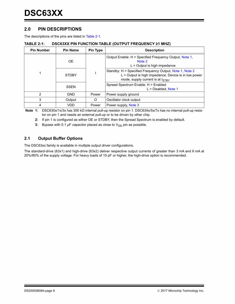
TABLE 2-1: DSC63XX PIN FUNCTION TABLE (OUTPUT FREQUENCY ≥1 MHZ)
Pin Number Pin Name Pin Type Description
1
OE
I
Output Enable: H = Specified Frequency Output, Note 1, Note 2 L = Output is high impedance
STDBYStandby: H = Specified Frequency Output, Note 1, Note 2
L = Output is high impedance. Device is in low power mode, supply current is at ISTBY
SSENSpread Spectrum Enable: H = Enabled L = Disabled, Note 1
2 GND Power Power supply ground
3 Output O Oscillator clock output
4 VDD Power Power supply, Note 3
Note 1: DSC630x/1x/3x has 300 kΩ internal pull-up resistor on pin 1. DSC634x/5x/7x has no internal pull-up resis-tor on pin 1 and needs an external pull-up or to be driven by other chip.
2: If pin 1 is configured as either OE or STDBY, then the Spread Spectrum is enabled by default.
3: Bypass with 0.1 µF capacitor placed as close to VDD pin as possible.
2017 Microchip Technology Inc. DS20005808A-page 7
DSC63XX
3.0 DIAGRAMS
FIGURE 3-1: Output Waveform.
FIGURE 3-2: Test Circuit.
FIGURE 3-3: Recommended Board Layout.
VOH
VOL
VIL
1/fo
OUTPUT
ENABLE
tDA
tEN
tFtR
VIH
VDD 0.1μF
4 3
1 2
VDA
IDD
CL
VDD
C1
GNDEnable
Output
Via to GND Layer
Via to GND Layer
DSC63XX
DS20005808A-page 8 2017 Microchip Technology Inc.
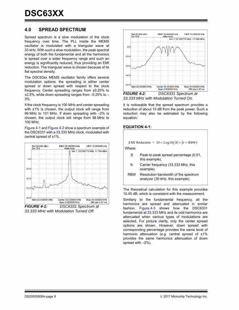
4.0 SPREAD SPECTRUM
Spread spectrum is a slow modulation of the clockfrequency over time. The PLL inside the MEMSoscillator is modulated with a triangular wave at33 kHz. With such a slow modulation, the peak spectralenergy of both the fundamental and all the harmonicsis spread over a wider frequency range and such anenergy is significantly reduced, thus providing an EMIreduction. The triangular wave is chosen because of itsflat spectral density.
The DSC63xx MEMS oscillator family offers severalmodulation options: the spreading is either centerspread or down spread with respect to the clockfrequency. Center spreading ranges from ±0.25% to±2.5%, while down spreading ranges from –0.25% to –3%.
If the clock frequency is 100 MHz and center spreadingwith ±1% is chosen, the output clock will range from99 MHz to 101 MHz. If down spreading with –2% ischosen, the output clock will range from 98 MHz to100 MHz.
Figure 4-1 and Figure 4-2 show a spectrum example ofthe DSC6331 with a 33.333 MHz clock, modulated withcentral spread of ±1%.
FIGURE 4-1: DSC6331 Spectrum at 33.333 MHz with Modulation Turned Off.
FIGURE 4-2: DSC6331 Spectrum at 33.333 MHz with Modulation Turned On.
It is noticeable that the spread spectrum provides areduction of about 10 dB from the peak power. Such areduction may also be estimated by the followingequation:
EQUATION 4-1:
The theoretical calculation for this example provides10.45 dB, which is consistent with the measurement.
Similarly to the fundamental frequency, all theharmonics are spread and attenuated in similarfashion. Figure 4-3 shows how the DSC6331fundamental at 33.333 MHz and its odd harmonics areattenuated when various types of modulations areselected. For picture clarity, only the center spreadoptions are shown. However, down spread withcorresponding percentage provides the same level ofharmonic attenuation (e.g. central spread of ±1%provides the same harmonics attenuation of downspread with –2%).
EMI Reduction 10 Log10 S fc RBW =
Where:
S Peak-to-peak spread percentage (0.01, this example).
fc Carrier frequency (33.333 Mhz, this example).
RBW Resolution bandwidth of the spectrum analyzer (30 kHz, this example).
2017 Microchip Technology Inc. DS20005808A-page 9
DSC63XX
FIGURE 4-3: DSC6331 Harmonic Levels with Various Spread Spectrum Options.
DSC63XX
DS20005808A-page 10 2017 Microchip Technology Inc.
5.0 SOLDER REFLOW
FIGURE 5-1: Solder Reflow Profile.
60-180SecondsTe
mpe
ratu
re (
°C)
260°C
3°C/se
c max
.
217°C200°C
150°C
25°C
8 minutes max.
Pre-Heat
3°C/se
c max
.
Reflow
Cool
Time6°C/sec m
ax.
60-150Seconds
20-40Seconds
MSL 1 @ 260°C refer to JSTD-020CRamp-Up Rate (200°C to Peak Temp) 3°C/sec max.
Pre-heat Time 150°C to 200°C 60 to 180 sec.
Time maintained above 217°C 60 to 150 sec.
Peak Temperature 255°C to 260°C
Time within 5°C of actual Peak 20 to 40 sec.
Ramp-Down Rate 6°C/sec. max.
Time 25°C to Peak Temperature 8 minutes max.
2017 Microchip Technology Inc. DS20005808A-page 11
DSC63XX
6.0 PACKAGING INFORMATION
6.1 Package Marking Information
XXXXXXX
Example4-Lead DFN*
SSSDCPYYWW
Example4-Lead VFLGA*
0333333
943DCP1734
SSSXXXW
SSS0069
Legend: XX...X Product code, customer-specific information, or frequency in MHz without printed decimal point
Y Year code (last digit of calendar year)YY Year code (last 2 digits of calendar year)WW Week code (week of January 1 is week ‘01’)NNN Alphanumeric traceability code Pb-free JEDEC® designator for Matte Tin (Sn)* This package is Pb-free. The Pb-free JEDEC designator ( )
can be found on the outer packaging for this package.
, , Pin one index is identified by a dot, delta up, or delta down (trianglemark).
Note: In the event the full Microchip part number cannot be marked on one line, it willbe carried over to the next line, thus limiting the number of availablecharacters for customer-specific information. Package may or may not includethe corporate logo.
Underbar (_) and/or Overbar (⎯) symbol may not be to scale.
3e
3e
DSC63XX
DS20005808A-page 12 2017 Microchip Technology Inc.
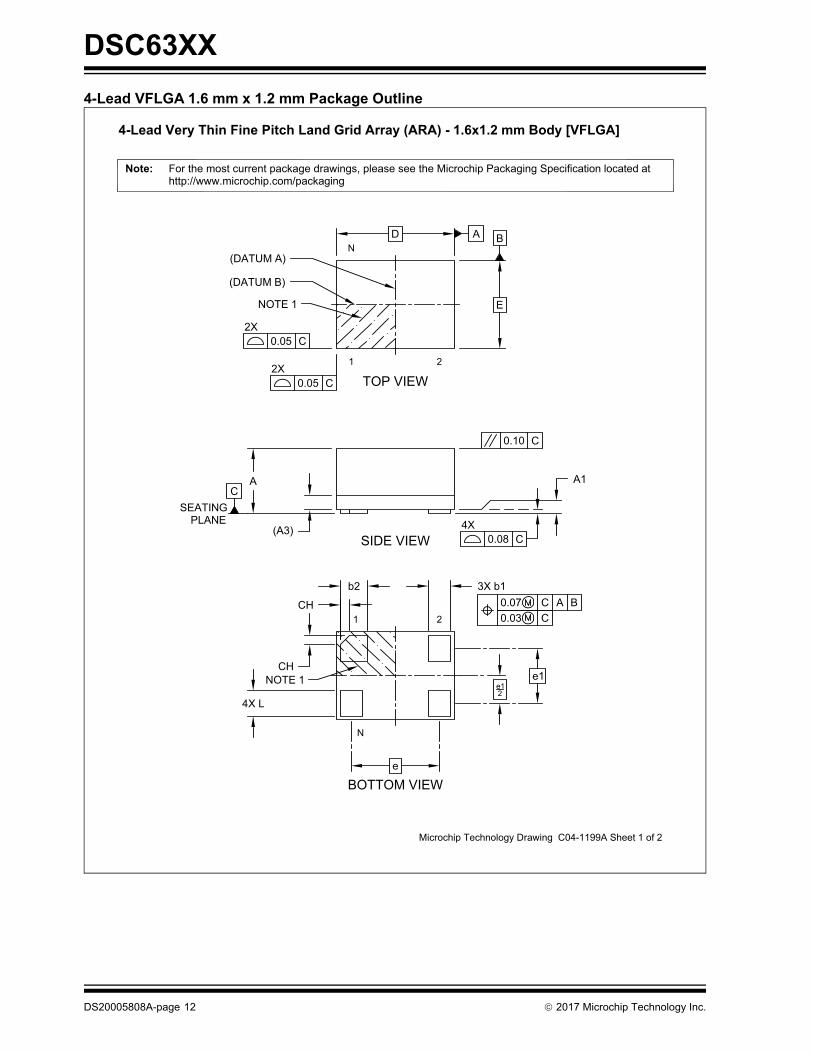
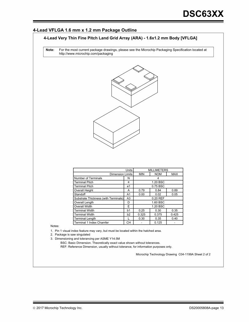
4-Lead VFLGA 1.6 mm x 1.2 mm Package Outline
0.07 C A B0.03 C
(DATUM B)
(DATUM A)
CSEATING
PLANE
NOTE 1
1 2
N
TOP VIEW
SIDE VIEW
BOTTOM VIEW
NOTE 1
1 2
N
0.10 C
0.08 C
Microchip Technology Drawing C04-1199A Sheet 1 of 2
4X
For the most current package drawings, please see the Microchip Packaging Specification located athttp://www.microchip.com/packaging
Note:
4-Lead Very Thin Fine Pitch Land Grid Array (ARA) - 1.6x1.2 mm Body [VFLGA]
D
E
BA
0.05 C
0.05 C2X
2X
4X L
b2
e
CH
CH
A
(A3)
A1
e1e12
3X b1
2017 Microchip Technology Inc. DS20005808A-page 13
DSC63XX
4-Lead VFLGA 1.6 mm x 1.2 mm Package Outline
Microchip Technology Drawing C04-1199A Sheet 2 of 2
REF: Reference Dimension, usually without tolerance, for information purposes only.BSC: Basic Dimension. Theoretically exact value shown without tolerances.
1.2.3.
Notes:
Pin 1 visual index feature may vary, but must be located within the hatched area.Package is saw singulatedDimensioning and tolerancing per ASME Y14.5M
4-Lead Very Thin Fine Pitch Land Grid Array (ARA) - 1.6x1.2 mm Body [VFLGA]
For the most current package drawings, please see the Microchip Packaging Specification located athttp://www.microchip.com/packaging
Note:
Number of Terminals
Overall Height
Overall Width
Terminal Length
Substrate Thickness (with Terminals)
Terminal Pitch
Standoff
UnitsDimension Limits
A1A
b2
A3
e
L
E
N1.20 BSC
0.20 REF
0.3250.30
0.790.00
0.350.375
0.840.02
1.20 BSC
MILLIMETERSMIN NOM
4
0.4250.40
0.890.05
MAX
CH 0.125- -Terminal 1 Index Chamfer
Overall Length D 1.60 BSC
Terminal Widthb1 0.25 0.30 0.35Terminal Width
Terminal Pitch e1 0.75 BSC
DSC63XX
DS20005808A-page 14 2017 Microchip Technology Inc.
4-Lead VFLGA 1.6 mm x 1.2 mm Recommended Land Pattern
RECOMMENDED LAND PATTERN
Dimension LimitsUnits
X2Contact Width
Contact Pitch
MILLIMETERS
1.20 BSCMIN
E1MAX
Space Between Contacts (X4)Contact Pad Length (X6)
G1Y 0.50
Microchip Technology Drawing C04-3199A
NOM
4-Lead Very Thin Fine Pitch Land Grid Array (ARA) - 1.6x1.2 mm Body [VFLGA]
SILK SCREEN
1 2
4
X1Contact Width (X3)
Space Between Contacts (X3) G2 0.25
BSC: Basic Dimension. Theoretically exact value shown without tolerances.
Notes:Dimensioning and tolerancing per ASME Y14.5M1.
For the most current package drawings, please see the Microchip Packaging Specification located athttp://www.microchip.com/packaging
Note:
X1
Y
G2
(CH)
CContact Spacing 0.75
0.430.35
0.85
Contact 1 Index Chamfer CH 0.13 X 45° REF
C
E2
Contact Pitch 1.16 BSCE2
X2
G1
E1
2017 Microchip Technology Inc. DS20005808A-page 15
DSC63XX
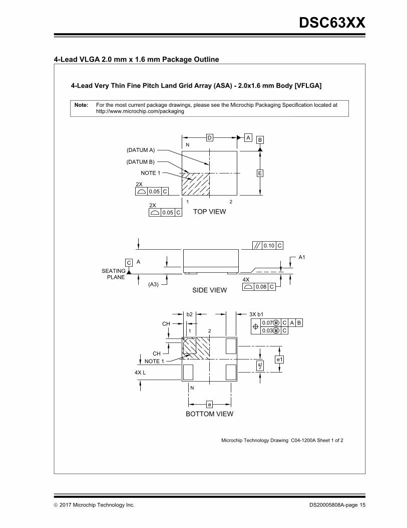
4-Lead VLGA 2.0 mm x 1.6 mm Package Outline
0.07 C A B0.03 C
(DATUM B)
(DATUM A)
CSEATING
PLANE
NOTE 1
1 2
N
TOP VIEW
SIDE VIEW
BOTTOM VIEW
NOTE 1
1 2
N
0.10 C
0.08 C
Microchip Technology Drawing C04-1200A Sheet 1 of 2
4X
For the most current package drawings, please see the Microchip Packaging Specification located athttp://www.microchip.com/packaging
Note:
4-Lead Very Thin Fine Pitch Land Grid Array (ASA) - 2.0x1.6 mm Body [VFLGA]
D
E
BA
0.05 C
0.05 C2X
2X
4X L
b2
e
CH
CH
A
(A3)
A1
e1e12
3X b1
DSC63XX
DS20005808A-page 16 2017 Microchip Technology Inc.
4-Lead VLGA 2.0 mm x 1.6 mm Package Outline (Continued)
Microchip Technology Drawing C04-1200A Sheet 2 of 2
REF: Reference Dimension, usually without tolerance, for information purposes only.BSC: Basic Dimension. Theoretically exact value shown without tolerances.
1.2.3.
Notes:
Pin 1 visual index feature may vary, but must be located within the hatched area.Package is saw singulatedDimensioning and tolerancing per ASME Y14.5M
4-Lead Very Thin Fine Pitch Land Grid Array (ASA) - 2.0x1.6 mm Body [VFLGA]
For the most current package drawings, please see the Microchip Packaging Specification located athttp://www.microchip.com/packaging
Note:
Number of Terminals
Overall Height
Overall Width
Terminal Length
Substrate Thickness (with Terminals)
Terminal Pitch
Standoff
UnitsDimension Limits
A1A
b2
A3
e
L
E
N1.55 BSC
0.20 REF
0.400.50
0.790.00
0.550.45
0.840.02
1.60 BSC
MILLIMETERSMIN NOM
6
0.500.60
0.890.05
MAX
CH 0.15- -Terminal 1 Index Chamfer
Overall Length D 2.00 BSC
Terminal Widthb1 0.30 0.35 0.40Terminal Width
Terminal Pitch e1 0.95 BSC
2017 Microchip Technology Inc. DS20005808A-page 17
DSC63XX
4-Lead VFLGA 2.0 mm x 1.6 mm Package Outline
RECOMMENDED LAND PATTERN
Dimension LimitsUnits
X2Contact Width (X2)
Contact Pitch
MILLIMETERS
1.55 BSCMIN
EMAX
Space Between Contacts (X4)Contact Pad Length (X6)
G1Y 0.70
Microchip Technology Drawing C04-3200A
NOM
4-Lead Very Thin Fine Pitch Land Grid Array (ASA) - 2.0x1.6 mm Body [VFLGA]
SILK SCREEN
1 2
4
X1Contact Width (X4)
Space Between Contacts (X3) G2 0.25
BSC: Basic Dimension. Theoretically exact value shown without tolerances.
Notes:Dimensioning and tolerancing per ASME Y14.5M1.
For the most current package drawings, please see the Microchip Packaging Specification located athttp://www.microchip.com/packaging
Note:
X1
Y G2
G1
E
(CH)
CContact Spacing 0.95
0.400.50
1.05
Contact 1 Index Chamfer CH 0.13 X 45° REF
C
DSC63XX
DS20005808A-page 18 2017 Microchip Technology Inc.
4-Lead VLGA 2.5 mm x 2.0 mm Package Outline
0.07 C A B0.03 C
(DATUM B)
(DATUM A)
CSEATING
PLANE
NOTE 1
1 2
N
TOP VIEW
SIDE VIEW
BOTTOM VIEW
NOTE 1
1 2
N
0.10 C
0.08 C
Microchip Technology Drawing C04-1202A Sheet 1 of 2
4X
For the most current package drawings, please see the Microchip Packaging Specification located athttp://www.microchip.com/packaging
Note:
4-Lead Very Thin Land Grid Array (AUA) - 2.5x2.0 mm Body [VLGA]
D
E
BA
0.05 C
0.05 C2X
2X
4X L
e
CH
CH
A
(A3)
A1
e1e12
4X b1
2017 Microchip Technology Inc. DS20005808A-page 19
DSC63XX
4-Lead VLGA 2.5 mm x 2.0 mm Package Outline (Continued)
Microchip Technology Drawing C04-1202A Sheet 2 of 2
REF: Reference Dimension, usually without tolerance, for information purposes only.BSC: Basic Dimension. Theoretically exact value shown without tolerances.
1.2.3.
Notes:
Pin 1 visual index feature may vary, but must be located within the hatched area.Package is saw singulatedDimensioning and tolerancing per ASME Y14.5M
4-Lead Very Thin Land Grid Array (AUA) - 2.5x2.0 mm Body [VLGA]
For the most current package drawings, please see the Microchip Packaging Specification located athttp://www.microchip.com/packaging
Note:
Number of Terminals
Overall Height
Overall Width
Terminal Length
Substrate Thickness (with Terminals)
Terminal Pitch
Standoff
UnitsDimension Limits
A1A
A3
e
L
E
N1.65 BSC
0.20 REF
0.60
0.790.00
0.65
0.840.02
2.00 BSC
MILLIMETERSMIN NOM
4
0.70
0.890.05
MAX
CH 0.225- -Terminal 1 Index Chamfer
Overall Length D 2.50 BSC
b1 0.60 0.65 0.70Terminal Width
Terminal Pitch e1 1.25 BSC
DSC63XX
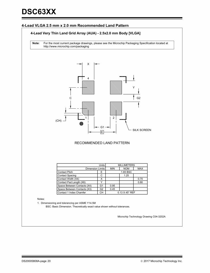
DS20005808A-page 20 2017 Microchip Technology Inc.
4-Lead VLGA 2.5 mm x 2.0 mm Recommended Land Pattern
RECOMMENDED LAND PATTERN
Dimension LimitsUnits
Contact Pitch
MILLIMETERS
1.65 BSCMIN
EMAX
Space Between Contacts (X4)Contact Pad Length (X6)
G1Y 0.80
Microchip Technology Drawing C04-3202A
NOM
4-Lead Very Thin Land Grid Array (AUA) - 2.5x2.0 mm Body [VLGA]
SILK SCREEN
1 2
4
XContact Width (X4)
Space Between Contacts (X3) G2 0.45
BSC: Basic Dimension. Theoretically exact value shown without tolerances.
Notes:Dimensioning and tolerancing per ASME Y14.5M1.
For the most current package drawings, please see the Microchip Packaging Specification located athttp://www.microchip.com/packaging
Note:
X
Y
G2C
E
(CH)
CContact Spacing 1.250.70
0.95
Contact 1 Index Chamfer CH 0.13 X 45° REF
G1
2017 Microchip Technology Inc. DS20005808A-page 21
DSC63XX
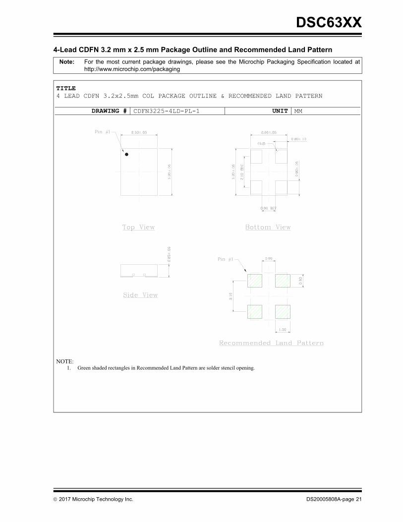
4-Lead CDFN 3.2 mm x 2.5 mm Package Outline and Recommended Land Pattern
Note: For the most current package drawings, please see the Microchip Packaging Specification located athttp://www.microchip.com/packaging
TITLE4 LEAD CDFN 3.2x2.5mm COL PACKAGE OUTLINE & RECOMMENDED LAND PATTERN
DRAWING # CDFN3225-4LD-PL-1 UNIT MM
NOTE:1. Green shaded rectangles in Recommended Land Pattern are solder stencil opening.
DSC63XX
DS20005808A-page 22 2017 Microchip Technology Inc.
NOTES:
2017 Microchip Technology Inc. DS20005808A-page 23
DSC63XX
APPENDIX A: REVISION HISTORY
Revision A (September 2017)
• Initial release of DSC63xx Microchip data sheet DS20005808A.
DSC63XX
DS20005808A-page 24 2017 Microchip Technology Inc.
NOTES:
2017 Microchip Technology Inc. DS20005808A-page 25
DSC63XX
PRODUCT IDENTIFICATION SYSTEM
To order or obtain information, e.g., on pricing or delivery, contact your local Microchip representative or sales office.
Note 1: Please visit Microchip ClockWorks® Configurator Website to configure the part number for customized fre-quency. http://clockworks.microchip.com/timing/.
Examples:
a) DSC6332JI2AA-100.0000:
Ultra–Low Power MEMS Oscillator, Pin1 = SpreadSpectrum Enable with Internal Pull-Up, High Drive Strength, 4-Lead 2.5 mm x 2.0 mm VFLGA, Industrial Temperature, ±25 ppm Stability, ±0.25% SpreadSpectrum, Revision A, 100 MHz Frequency, 110/Tube
b) DSC6301HE1HA-016.0000T:Ultra–Low Power MEMS Oscillator, Pin1 = OE with Internal Pull–Up, Standard Drive Strength, 4-Lead 1.6 mm x 1.2 mm VFLGA, Extended Commercial Temp., ±50 ppm Stability, –0.5% Spread Spectrum Revision A, 16 MHz Frequency, 1,000/Reel
Frequency: xxx.xxxx = User-Defined Frequency between 001.0000 MHz and 100.0000 MHz
Tape and Reel: <blank>= 110/TubeT = 1,000/Reel
X
Pin 1Definition
Note 1: Tape and Reel identifier only appears in the catalog part number description. This identifier is used for ordering purposes and is not printed on the device package. Check with your Microchip Sales Office for package availability with the Tape and Reel option.
X
OutputDrive
Strength
X
Temp.Range
X
Freq.Stability
X
Revision
XXX.XXXX
Frequency
X
TapeandReel
–X
SpreadSpectrum
DSC63XX
DS20005808A-page 26 2017 Microchip Technology Inc.
NOTES:
2017 Microchip Technology Inc. DS20005808A-page 27
Information contained in this publication regarding deviceapplications and the like is provided only for your convenienceand may be superseded by updates. It is your responsibility toensure that your application meets with your specifications.MICROCHIP MAKES NO REPRESENTATIONS ORWARRANTIES OF ANY KIND WHETHER EXPRESS ORIMPLIED, WRITTEN OR ORAL, STATUTORY OROTHERWISE, RELATED TO THE INFORMATION,INCLUDING BUT NOT LIMITED TO ITS CONDITION,QUALITY, PERFORMANCE, MERCHANTABILITY ORFITNESS FOR PURPOSE. Microchip disclaims all liabilityarising from this information and its use. Use of Microchipdevices in life support and/or safety applications is entirely atthe buyer’s risk, and the buyer agrees to defend, indemnify andhold harmless Microchip from any and all damages, claims,suits, or expenses resulting from such use. No licenses areconveyed, implicitly or otherwise, under any Microchipintellectual property rights unless otherwise stated.
Trademarks
The Microchip name and logo, the Microchip logo, AnyRate, AVR, AVR logo, AVR Freaks, BeaconThings, BitCloud, CryptoMemory, CryptoRF, dsPIC, FlashFlex, flexPWR, Heldo, JukeBlox, KEELOQ, KEELOQ logo, Kleer, LANCheck, LINK MD, maXStylus, maXTouch, MediaLB, megaAVR, MOST, MOST logo, MPLAB, OptoLyzer, PIC, picoPower, PICSTART, PIC32 logo, Prochip Designer, QTouch, RightTouch, SAM-BA, SpyNIC, SST, SST Logo, SuperFlash, tinyAVR, UNI/O, and XMEGA are registered trademarks of Microchip Technology Incorporated in the U.S.A. and other countries.
ClockWorks, The Embedded Control Solutions Company, EtherSynch, Hyper Speed Control, HyperLight Load, IntelliMOS, mTouch, Precision Edge, and Quiet-Wire are registered trademarks of Microchip Technology Incorporated in the U.S.A.
Adjacent Key Suppression, AKS, Analog-for-the-Digital Age, Any Capacitor, AnyIn, AnyOut, BodyCom, chipKIT, chipKIT logo, CodeGuard, CryptoAuthentication, CryptoCompanion, CryptoController, dsPICDEM, dsPICDEM.net, Dynamic Average Matching, DAM, ECAN, EtherGREEN, In-Circuit Serial Programming, ICSP, Inter-Chip Connectivity, JitterBlocker, KleerNet, KleerNet logo, Mindi, MiWi, motorBench, MPASM, MPF, MPLAB Certified logo, MPLIB, MPLINK, MultiTRAK, NetDetach, Omniscient Code Generation, PICDEM, PICDEM.net, PICkit, PICtail, PureSilicon, QMatrix, RightTouch logo, REAL ICE, Ripple Blocker, SAM-ICE, Serial Quad I/O, SMART-I.S., SQI, SuperSwitcher, SuperSwitcher II, Total Endurance, TSHARC, USBCheck, VariSense, ViewSpan, WiperLock, Wireless DNA, and ZENA are trademarks of Microchip Technology Incorporated in the U.S.A. and other countries.
SQTP is a service mark of Microchip Technology Incorporated in the U.S.A.
Silicon Storage Technology is a registered trademark of Microchip Technology Inc. in other countries.
GestIC is a registered trademark of Microchip Technology Germany II GmbH & Co. KG, a subsidiary of Microchip Technology Inc., in other countries.
All other trademarks mentioned herein are property of their respective companies.
Note the following details of the code protection feature on Microchip devices:
• Microchip products meet the specification contained in their particular Microchip Data Sheet.
• Microchip believes that its family of products is one of the most secure families of its kind on the market today, when used in the intended manner and under normal conditions.
• There are dishonest and possibly illegal methods used to breach the code protection feature. All of these methods, to our knowledge, require using the Microchip products in a manner outside the operating specifications contained in Microchip’s Data Sheets. Most likely, the person doing so is engaged in theft of intellectual property.
• Microchip is willing to work with the customer who is concerned about the integrity of their code.
• Neither Microchip nor any other semiconductor manufacturer can guarantee the security of their code. Code protection does not mean that we are guaranteeing the product as “unbreakable.”
Code protection is constantly evolving. We at Microchip are committed to continuously improving the code protection features of ourproducts. Attempts to break Microchip’s code protection feature may be a violation of the Digital Millennium Copyright Act. If such actsallow unauthorized access to your software or other copyrighted work, you may have a right to sue for relief under that Act.
Microchip received ISO/TS-16949:2009 certification for its worldwide headquarters, design and wafer fabrication facilities in Chandler and Tempe, Arizona; Gresham, Oregon and design centers in California and India. The Company’s quality system processes and procedures are for its PIC® MCUs and dsPIC® DSCs, KEELOQ® code hopping devices, Serial EEPROMs, microperipherals, nonvolatile memory and analog products. In addition, Microchip’s quality system for the design and manufacture of development systems is ISO 9001:2000 certified.
QUALITYMANAGEMENTSYSTEMCERTIFIEDBYDNV
== ISO/TS16949==
DS20005808A-page 28 2017 Microchip Technology Inc.
AMERICASCorporate Office2355 West Chandler Blvd.Chandler, AZ 85224-6199Tel: 480-792-7200 Fax: 480-792-7277Technical Support: http://www.microchip.com/supportWeb Address: www.microchip.com
AtlantaDuluth, GA Tel: 678-957-9614 Fax: 678-957-1455
Austin, TXTel: 512-257-3370
BostonWestborough, MA Tel: 774-760-0087 Fax: 774-760-0088
ChicagoItasca, IL Tel: 630-285-0071 Fax: 630-285-0075