SANDIA REPORT SAND2009-4069 Unlimited Release Printed Month and Year Ultra-thin Multilayer Capacitors Todd C. Monson Timothy Jerome Renk Prepared by Sandia National Laboratories Albuquerque, New Mexico 87185 and Livermore, California 94550 Sandia is a multiprogram laboratory operated by Sandia Corporation, a Lockheed Martin Company, for the United States Department of Energy’s National Nuclear Security Administration under Contract DE-AC04-94AL85000. Approved for public release; further dissemination unlimited.
Transcript
SANDIA REPORT SAND2009-4069 Unlimited Release Printed Month and Year
Ultra-thin Multilayer Capacitors Todd C. Monson Timothy Jerome Renk Prepared by Sandia National Laboratories Albuquerque, New Mexico 87185 and Livermore, California 94550 Sandia is a multiprogram laboratory operated by Sandia Corporation, a Lockheed Martin Company, for the United States Department of Energy’s National Nuclear Security Administration under Contract DE-AC04-94AL85000. Approved for public release; further dissemination unlimited.
Issued by Sandia National Laboratories, operated for the United States Department of Energy by Sandia Corporation. NOTICE: This report was prepared as an account of work sponsored by an agency of the United States Government. Neither the United States Government, nor any agency thereof, nor any of their employees, nor any of their contractors, subcontractors, or their employees, make any warranty, express or implied, or assume any legal liability or responsibility for the accuracy, completeness, or usefulness of any information, apparatus, product, or process disclosed, or represent that its use would not infringe privately owned rights. Reference herein to any specific commercial product, process, or service by trade name, trademark, manufacturer, or otherwise, does not necessarily constitute or imply its endorsement, recommendation, or favoring by the United States Government, any agency thereof, or any of their contractors or subcontractors. The views and opinions expressed herein do not necessarily state or reflect those of the United States Government, any agency thereof, or any of their contractors. Printed in the United States of America. This report has been reproduced directly from the best available copy. Available to DOE and DOE contractors from U.S. Department of Energy Office of Scientific and Technical Information P.O. Box 62 Oak Ridge, TN 37831 Telephone: (865) 576-8401 Facsimile: (865) 576-5728 E-Mail: [email protected] Online ordering: http://www.osti.gov/bridge Available to the public from U.S. Department of Commerce National Technical Information Service 5285 Port Royal Rd. Springfield, VA 22161 Telephone: (800) 553-6847 Facsimile: (703) 605-6900 E-Mail: [email protected] Online order: http://www.ntis.gov/help/ordermethods.asp?loc=7-4-0#online
The fabrication of ultra-thin lanthanum-doped lead zirconium titanate (PLZT) multilayer ceramic capacitors (MLCCs) using a high-power pulsed ion beam was studied. The deposition experiments were conducted on the RHEPP-1 facility at Sandia National Laboratories. The goal of this work was to increase the energy density of ceramic capacitors through the formation of a multilayer device with excellent materials properties, dielectric constant, and standoff voltage. For successful device construction, there are a number of challenging requirements including achieving correct stoichiometric and crystallographic composition of the deposited PLZT, as well as the creation of a defect free homogenous film. This report details some success in satisfying these requirements, although 900 °C temperatures were necessary for PLZT perovskite phase formation. These temperatures were applied to a previously deposited multi-layer film which was then post-annealed to this temperature. The film exhibited mechanical distress attributable to differences in the coefficient of thermal expansion (CTE) of the various layers. This caused significant defects in the deposited films that led to shorts across devices. A follow-on single layer deposition without post-anneal produced smooth layers with good interface behavior, but without the perovskite phase formation. These issues will need to be addressed in order for ion beam deposited MLCCs to become a viable technology. It is possible that future in-situ heating during deposition may address both the CTE issue, and result in lowered processing temperatures, which in turn could raise the probability of successful MLCC formation.
3
4
ACKNOWLEDGMENTS The authors wish to thank Donald L. Overmyer for his help in collecting X-ray diffraction (XRD) data, Tyler E. Stevens for assistance with sample annealing, Paula Provencio for collecting SEM and TEM images, and Gerard. A. Torres for technical assistance in the RHEPP-1 deposition experiments.
2. Description of RHEPP-1 and Experimental Setup .................................................................. 13
3. Experimental Results ............................................................................................................... 16 3.1. Deposition and Analysis of Initial PLZT Film ............................................................. 16 3.2. Addition of Extra Lead and Formation of Crystalline PLZT ....................................... 18 3.3. Multilayer Device Fabrication and Characterization .................................................... 21
4. Discussion and Conclusions ..................................................................................................... 25
Distribution ................................................................................................................................... 29
FIGURES Figure 1. Conceptual drawing of multilayer capacitor structure ................................................. 10 Figure 2. Marx and pulse-forming line ........................................................................................ 14 Figure 3. LIVA (top) and vacuum chamber (bottom) .................................................................. 14 Figure 4. Side-view of the diode with MAP ion source and beam transport region. ................... 15 Figure 5. XRD data of films produced using (Pb0.9La0.1Zr0.65Ti0.35)O3 target ............................. 17 Figure 6. PLZT target (left) with Pb target (right) ....................................................................... 18 Figure 7. XRD data of PLZT films deposited with extra lead at room temperature and post-annealed at 650 °C for 1, 5, and 10 min. The strongest diffraction peaks for (Pb0.9La0.1Zr0.65Ti0.35)O3, sapphire (substrate material), PbO (litharge), and Pb are displayed in the lower portion of the figure. ..................................................................................................... 19 Figure 8. XRD patterns for PLZT films deposited with extra lead and annealed at 900 °C for 10 and 30 min. and compared to the target material and a film annealed at 650 °C for 5 min. ........ 20 Figure 9. Comparison of film post-annealed at 900°C for 10 min. with the PLZT target. .......... 20 Figure 10. Diagram of successive layers of deposited electrode and dielectric material. ........... 22 Figure 11. SEM image of MLCC after etching with FIB. ........................................................... 23 Figure 12. XTEM image of MLCC after etching with FIB. The results of elemental analysis from EDS are labeled. ................................................................................................................... 24 Figure 13. XTEM image of MLCC after etching with FIB. The results of elemental analysis from EDS are labeled. ................................................................................................................... 25
6
NOMENCLATURE DOE Department of Energy EDS Energy Dispersive X-ray Spectroscopy FIB Focused Ion Beam HEV Hybrid Electric Vehicle LIVA Linear Induction Voltage Adder MAP Magnetically Injected Plasma MLCC Multilayer Ceramic Capacitor PLD Pulsed Laser Deposition PIBD Pulsed Ion Beam Deposition PLZT Lanthanum-Doped Lead Zirconium Titanate PVD Physical Vapor Deposition RHEPP-1 Repetitive High Energy Pulsed Power RTBF Readiness in Technical Base and Facilities RT Room Temperature SEM Scanning Electron Microscope SNL Sandia National Laboratories TEM Transmission Electron Microscope XRD X-ray Diffraction XTEM Cross-Sectional Transmission Electron Microscopy
7
1. INTRODUCTION Multilayer ceramic capacitors (MLCCs) have the opportunity to meet a variety of needs where energy storage must meet volumetric restrictions. MLCCs are also capable of providing significant peak power for pulsed energy applications. Applications are diverse and range from energy storage in portable electronic devices, electromagnetic launchers, fuzing applications, and implantable medical devices. Electric and hybrid electric vehicles (HEVs) could benefit from the reduced volume required for energy storage in improved MLCCs and the high peak power they can offer. Additionally, multi-stage accelerators could be made significantly smaller, if the energy storage density of batteries and capacitors is reduced. Current energy density limits for MLCCs are on the order of a few J/cc or less. To make significant progress in advancing a number of technologies, energy density targets of 10 J/cc are required. One way to achieve high energy density capacitors is to combine numerous sub-layers of very thin dielectric material (as little as 10 nm thick) separated by metal layers and energize them in parallel. This can be as follows: The capacitance of a multilayer capacitor of n layers each of area A is C = nεA/d where ε is the dielectric constant of each layer of dielectric material of thickness d. Consequently, the capacitance can be increased by increasing the number of layers, and by decreasing each layer thickness (as long as dielectric breakdown does not occur). Current approaches to capacitor construction have difficulty scaling down to the 10 nm per layer thickness. Liquid processing (e.g. solgel) cannot achieve this level of thinness. Conventional physical vapor deposition (PVD) techniques such as magnetron sputtering can lead to layers as thin as 10 nm each. However, deposition rates for sputtering (Å per second) are relatively slow, and if layer heating is required during the deposition process, the result can be inter-diffusion of the layer materials. The microstructure of sputtered layers also tends to exhibit columnar grain growth. Both of these effects can lead to reduced standoff voltage or otherwise compromised performance of the multilayer capacitor structure. The tape casting process that industry currently uses to form MLCCs produces layers that are on the order of a μm or greater. Here, an alternate approach to thin film layer formation was investigated. A pulsed high-power ion beam impinged on various target materials with energies sufficient to vaporize the surface and create a blow-off plasma, which then deposits some distance away on a chosen substrate. The ion beam is generated by the 800 kV RHEPP-1 facility at Sandia. The advantage of this Pulsed Ion Beam Deposition (PIBD) process over magnetron sputtering lies in the volume of deposited material, the rate of deposition, and the resultant microstructure of the deposited layer. Each ion beam pulse can lead to layer thicknesses from 1 to 100 nm over areas tens of cm2. Previous PIBD deposition experiments using RHEPP-1[1] have yielded high-quality thin layers of fine-grain or amorphous microstructure, which in particular lacked the columnar structure seen on sputtered layers. This can be attributed in part to the
8
high kinetic energy of the ablation plasma, estimated at tens of eV compared to fractions of an eV for plasmas formed by magnetron sputtering. Pulsed laser deposition (PLD), which uses lasers to ablate surface materials, also produces high kinetic energy ablation plasmas. However, the laser power needed to ablate materials requires a highly focused beam (~ few mm2) for lasers of reasonable size. This small spot size leads to low deposition rates (~ Å/sec) even for repetitively pulsed lasers, similar to that produced by sputtering. By contrast, the high-power RHEPP ion beam delivers a focused beam of up to 1 kJ of energy to a target material, leading to ablated materials produced over ~ 30 cm2 of target area and deposition rates over two orders of magnitude higher than with PLD. The RHEPP-1 PIBD process then combines the high kinetics of laser ablation with potentially high volume production. The thin-film materials chosen for this project consist of the following:
1. Dielectric source material: lanthanum-doped lead zirconium titanate (PLZT). This material was chosen because it is the object of current investigation at Sandia, and formulations of this material have exhibited energy densities of up to 7 J/cc [2]. The stoichiometry of this material is quite complex, with the highest performing compositions of proprietary chemical formulation. The high dielectric properties of this material only occur for the crystalline perovskite phase.
2. Electrode material: This is a metal which forms the conductive layers that separate layers of
dielectric material. The metal must have good electrical conductivity, a high melting point (to withstand any post-annealing temperatures without melting or diffusing into the dielectric layer), and in general should have properties of a noble metal to resist oxidation of the electrode tabs which must be connected to external circuitry. We chose rhodium for the electrode material. This was chosen instead of platinum, which is also a good candidate material, because Rh was already acquired, whereas Pt would be very expensive to purchase. Rh actually has a higher melting point and higher electrical conductivity than Pt, and is known to be highly resistant to corrosion.
3. Substrate. The substrate chosen was polished sapphire (Al2O3), chosen because it has a high
melting point, is electrically insulating, and can be polished to a smooth surface (± 0.001 in.) The requirements for a high quality layered capacitor can be separated into two groups:
1) Dielectric material quality. The deposited PLZT must be of the correct stoichiometry, i.e. the proportion of the constituent elements must be correct and it must be homogenous. The crystalline structure of the PLZT must be the perovskite phase. Finally, the material must be fully dense and free of pinholes, so as to hold off applied voltages without breakdown.
2) Multilayer mechanical quality. The dielectric must demonstrate good intra-layer adhesion with
9
the alternating electrode layers and the interfaces between the dielectric and electrodes must be clean and free of interdiffusional phase material. The electrode materials must be connectable to external circuitry for delivery of input voltage and power. Additionally, the multilayer film must be stably attached to the substrate and the resulting structure must exhibit both a high dielectric constant and breakdown strength.
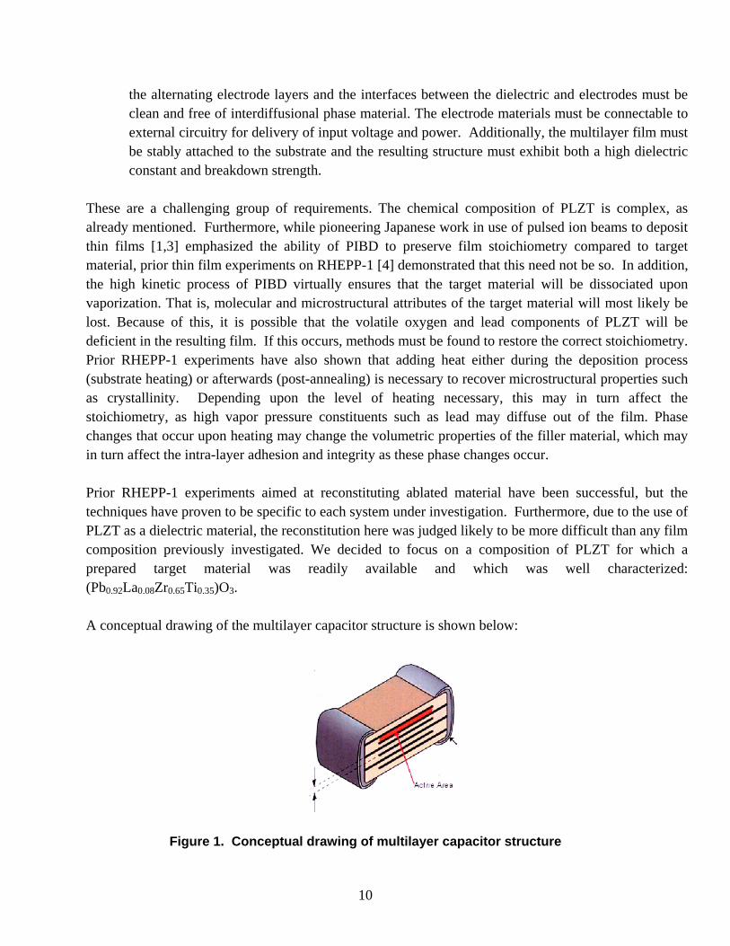
These are a challenging group of requirements. The chemical composition of PLZT is complex, as already mentioned. Furthermore, while pioneering Japanese work in use of pulsed ion beams to deposit thin films [1,3] emphasized the ability of PIBD to preserve film stoichiometry compared to target material, prior thin film experiments on RHEPP-1 [4] demonstrated that this need not be so. In addition, the high kinetic process of PIBD virtually ensures that the target material will be dissociated upon vaporization. That is, molecular and microstructural attributes of the target material will most likely be lost. Because of this, it is possible that the volatile oxygen and lead components of PLZT will be deficient in the resulting film. If this occurs, methods must be found to restore the correct stoichiometry. Prior RHEPP-1 experiments have also shown that adding heat either during the deposition process (substrate heating) or afterwards (post-annealing) is necessary to recover microstructural properties such as crystallinity. Depending upon the level of heating necessary, this may in turn affect the stoichiometry, as high vapor pressure constituents such as lead may diffuse out of the film. Phase changes that occur upon heating may change the volumetric properties of the filler material, which may in turn affect the intra-layer adhesion and integrity as these phase changes occur. Prior RHEPP-1 experiments aimed at reconstituting ablated material have been successful, but the techniques have proven to be specific to each system under investigation. Furthermore, due to the use of PLZT as a dielectric material, the reconstitution here was judged likely to be more difficult than any film composition previously investigated. We decided to focus on a composition of PLZT for which a prepared target material was readily available and which was well characterized: (Pb0.92La0.08Zr0.65Ti0.35)O3. A conceptual drawing of the multilayer capacitor structure is shown below:
Figure 1. Conceptual drawing of multilayer capacitor structure
10
Note that a) the filler material must extend beyond the boundaries of the electrode material, or else shorting between the electrodes will occur, and 2) each electrode must include a tab for connection to external circuitry. In addition, each alternating electrode must extend in opposite directions, to allow the left and right side of the capacitor shown above to be attached to different external circuit components. Thus there are three differently shaped masks that must be utilized to construct the multilayer circuit. We at first investigated the possibility of engineering an in-situ motorized mask support, with each mask being rotated into position with control circuitry outside the deposition vacuum chamber. It quickly became apparent that the engineering for this would be challenging and costly, and we decided to make the films necessary for this project by manual masking using stainless steel cutouts placed close to the substrate surface. This approach requires changing out of the masks with each deposited layer, and hence the necessity of bringing the vacuum chamber up to normal air pressure to change the masks. The result is an increase in deposition time, and a slight additional risk of intralayer contamination by repeated exposure to atmospheric conditions. The project experimental plan was divided into several sections which will be discussed in detail in Section 3:
1) After obtaining the target PLZT material and sapphire substrates, we deposited an initial PLZT layer without electrode material under several different conditions intended to investigate the ability of heating mechanisms to reconstitute the PLZT material in the thin film. These include: a) in-situ heating at 350 °C during the deposition process, b) post-anneal in vacuum at 550 °C after deposition, and c) removal of the film followed by post-annealing in an oven located in Bldg 897.
2) Post-analysis of the deposited film with X-ray diffraction (XRD) showed that none of
the heating techniques resulted in film reconstitution. The oven post-anneal showed promise, but only at a post-anneal temperature of 1100 °C. This high heating level led to a serious deficiency in deposited lead fraction. This might be expected given the low melting point and high vapor pressure of lead.
3) We then obtained a separate lead target, and added it to the PLZT target material to
form a composite PLZT-Pb target. A second film was then deposited, followed by post-analysis which showed a good match to the PLZT target material, when it was post-annealed at 900 °C for 10 min. using a double crucible technique (to minimize Pb loss).
4) We fabricated a MLCC and subjected the device to the 900 °C post-anneal conditions
for 10 min. This device was examined using cross-sectional transmission electron microscopy (XTEM). Subsequent electrical measurements resulted in an electrical short.
11
5) Several single layer ceramic capacitors were fabricated and their electrical properties
were measured. All devices were shorted. These devices were also characterized using XTEM and energy dispersive X-ray spectroscopy (EDS)
Section 2 begins with a short description of the RHEPP-I ion beam and the geometry for the deposition experiments, followed by a detailed discussion of the experiments completed.
12
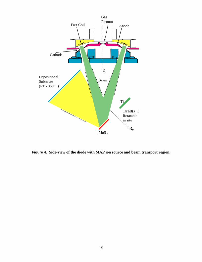
2. DESCRIPTION OF RHEPP-1 AND EXPERIMENTAL SETUP The RHEPP-1 pulsed ion beam facility is located in the Bldg. 970 Medium Bay at Sandia National Laboratories. RHEPP-1 consists of a 5 kJ Marx and pulse-forming line (Fig. 2) feeding a 4-stage Linear Induction Voltage Adder (LIVA). The LIVA transfers pulsed power to an Applied-B in a magnetically insulated diode with a Magnetically injected Plasma (MAP) gas-breakdown ion source. The ion beam propagates downward into a 1-meter long vacuum chamber. The LIVA can be seen in the top potion of Fig. 3, while the vacuum chamber appears in the bottom portion of the same figure. The RHEPP-1 beam generation process has been discussed in detail elsewhere [1, 5], and we give only the highlights of that discussion here. A schematic side-view of the diode with MAP ion source and beam transport region is given in Fig. 4. The geometry is cylindrically symmetric, with a gas plenum mounted on the center-line behind the inner Cu anode (red). When the plenum is energized, gas flows radially outward in a gap region towards the space between the inner and outer Cu anode. Two magnetic field coils are built into the cathode-side hardware (blue), and are energized well before the gas plenum is opened and power pulse arrives. The insulation field provided by the cathode (‘slow’) coils insulates the anode-cathode (A-K) gap from electron loss current. Before the gas plenum is energized but long after the ‘slow’ field coil is fired, a ‘fast coil’ is triggered. The rising fast coil waveform has a superimposed RF ringing cycle. When the plenum gas arrives at the fast coil location, the RF field ionizes the gas, and the interaction between the ‘slow’ and ‘fast’ magnetic fields pushes the now-plasma into position for acceleration when the power pulse arrives. The annular-shaped beam is brought to a soft focus due to the 20 degree pitch in the anode design, and Faraday cups can be mounted in the focal region to measure the beam fluence.
13
Figure 2. Marx and pulse-forming line
Figure 3. LIVA (top) and vacuum chamber (bottom)
For deposition of the multilayer films, two ablation targets are mounted on a rotatable fixture at a 45° angle to the oncoming beam, as shown at the bottom of the Figure 4. The fixture allows for in-situ ablation from different targets without breaking vacuum. For the studies discussed here, the two targets were PLZT and Rh. In practice, a third Ti target is used for the first few depositions, to improve film adhesion to the substrate. The depositional substrate is located on the center-line of the ablation plume formed by the impinging of the RHEPP-1 beam on the ablation targets. The substrate can be heated up to 350 °C during film deposition, and as high as 450 °C in vacuum after deposition. The diode region and the ablation targets are separated by 45 cm, and the distance between target(s) and substrate is typically 30 cm. Additional details of RHEPP-1 experiments can be found in [6,7].
14
Figure 4. Side-view of the diode with MAP ion source and beam transport region.
Cathode
Target(s )Rotatablein situ
DepositionalSubstrate(RT - 350C )
AnodeFast Coil
Beam
MoS 2
Ti
C
GasPlenum
L
15
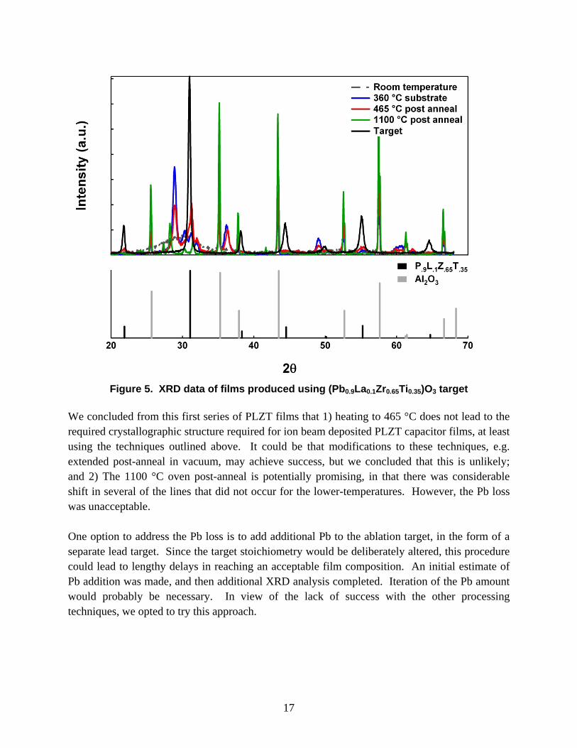
3. EXPERIMENTAL RESULTS 3.1. Deposition and Analysis of Initial PLZT Film A PLZT target of composition (Pb0.92La0.08Zr0.65Ti0.35)O3 was used to deposit an initial set of dielectric films. These films were examined using X-Ray diffraction (XRD) and compared to the target material in order to determine their composition and crystalline phase. The RHEPP-1 nitrogen beam was used to make this set of samples. The beam was intentionally attenuated so that the deposited layers would be thin, and 80 pulses were used (RHEPP-1 shots TJR25339 to TJR25421). Four dielectric films were made from this first deposition:
a) Room temperature (RT) deposition, substrate distance 30 cm.
b) RT deposition, followed by in-vacuum post-anneal at 465 °C for one hour.
c) RT deposition, followed by oven post-anneal at 1100 °C for 10 minutes.
d) deposition at 360 °C substrate temperature. The resulting XRD spectra, along with diffraction data collected from the target material, are shown in Fig. 5. The top part of this figure displays the spectra, and the bottom shows the expected spectral lines for a close match to the PLZT target ((Pb0.9La0.1Zr0.65Ti0.35)O3) and the sapphire substrate. Comparison of the spectra shows that none of the deposited films match the composition and crystalline phase of the target. The sapphire substrate shows clearly due to the thinness of the deposited films. None of the peaks at 2θ = 22°, 44.5°, 55° are evident in the deposited films. The prominent peak at 2θ = 31° is most evident in the 465° post-annealed film. However, additional analysis shows that this in-vacuum post-annealed film still consists mostly of constituent oxide materials like lead oxide. Further analysis revealed that the 1100 °C annealed film was very deficient in lead. This is probably due to the high post-anneal temperature. Evidence for this lead loss can be seen in the film thicknesses after processing, which were measured with a 1-D Dektak profilometer. The RT film measured 1.6 µm thick, as did the 465 °C annealed film. However, the 1100 °C post-annealed film measured only 1 µm in thickness, a substantial decrease.
16
Figure 5. XRD data of films produced using (Pb0.9La0.1Zr0.65Ti0.35)O3 target We concluded from this first series of PLZT films that 1) heating to 465 °C does not lead to the required crystallographic structure required for ion beam deposited PLZT capacitor films, at least using the techniques outlined above. It could be that modifications to these techniques, e.g. extended post-anneal in vacuum, may achieve success, but we concluded that this is unlikely; and 2) The 1100 °C oven post-anneal is potentially promising, in that there was considerable shift in several of the lines that did not occur for the lower-temperatures. However, the Pb loss was unacceptable. One option to address the Pb loss is to add additional Pb to the ablation target, in the form of a separate lead target. Since the target stoichiometry would be deliberately altered, this procedure could lead to lengthy delays in reaching an acceptable film composition. An initial estimate of Pb addition was made, and then additional XRD analysis completed. Iteration of the Pb amount would probably be necessary. In view of the lack of success with the other processing techniques, we opted to try this approach.
17
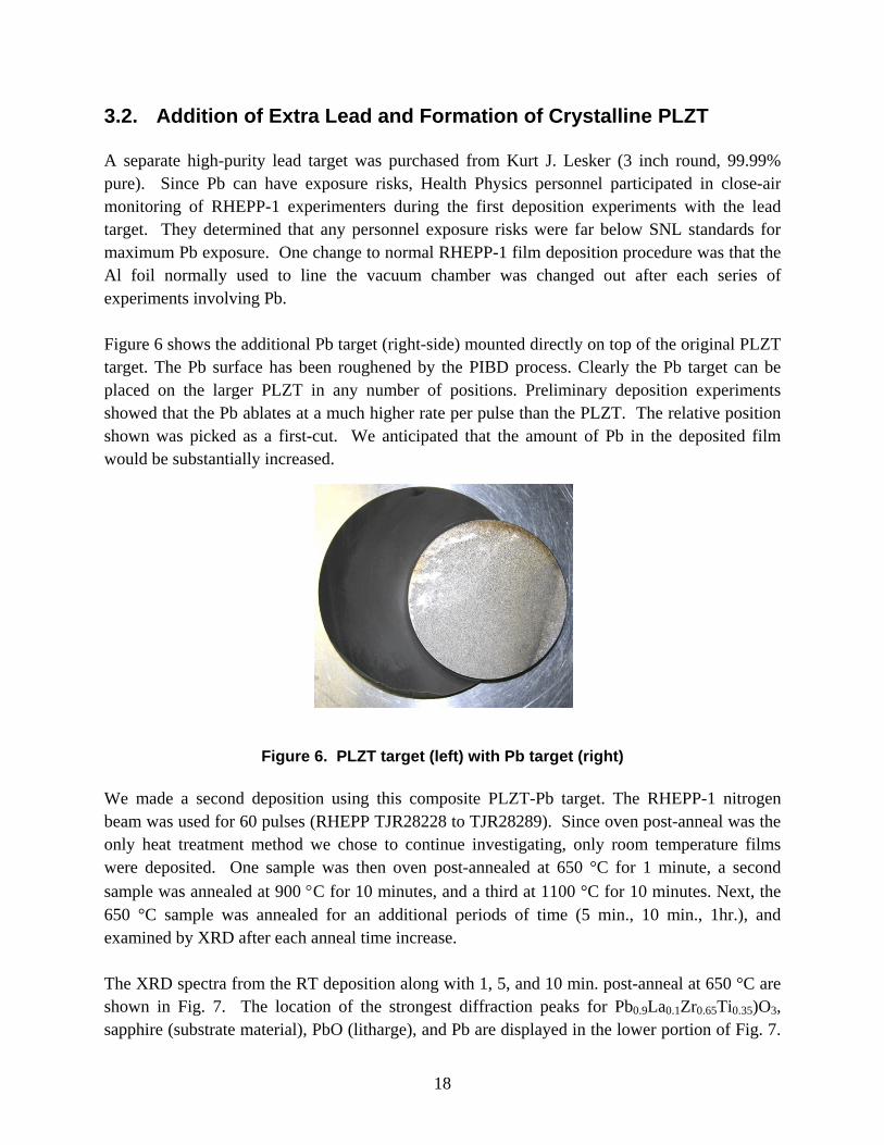
3.2. Addition of Extra Lead and Formation of Crystalline PLZT A separate high-purity lead target was purchased from Kurt J. Lesker (3 inch round, 99.99% pure). Since Pb can have exposure risks, Health Physics personnel participated in close-air monitoring of RHEPP-1 experimenters during the first deposition experiments with the lead target. They determined that any personnel exposure risks were far below SNL standards for maximum Pb exposure. One change to normal RHEPP-1 film deposition procedure was that the Al foil normally used to line the vacuum chamber was changed out after each series of experiments involving Pb. Figure 6 shows the additional Pb target (right-side) mounted directly on top of the original PLZT target. The Pb surface has been roughened by the PIBD process. Clearly the Pb target can be placed on the larger PLZT in any number of positions. Preliminary deposition experiments showed that the Pb ablates at a much higher rate per pulse than the PLZT. The relative position shown was picked as a first-cut. We anticipated that the amount of Pb in the deposited film would be substantially increased.
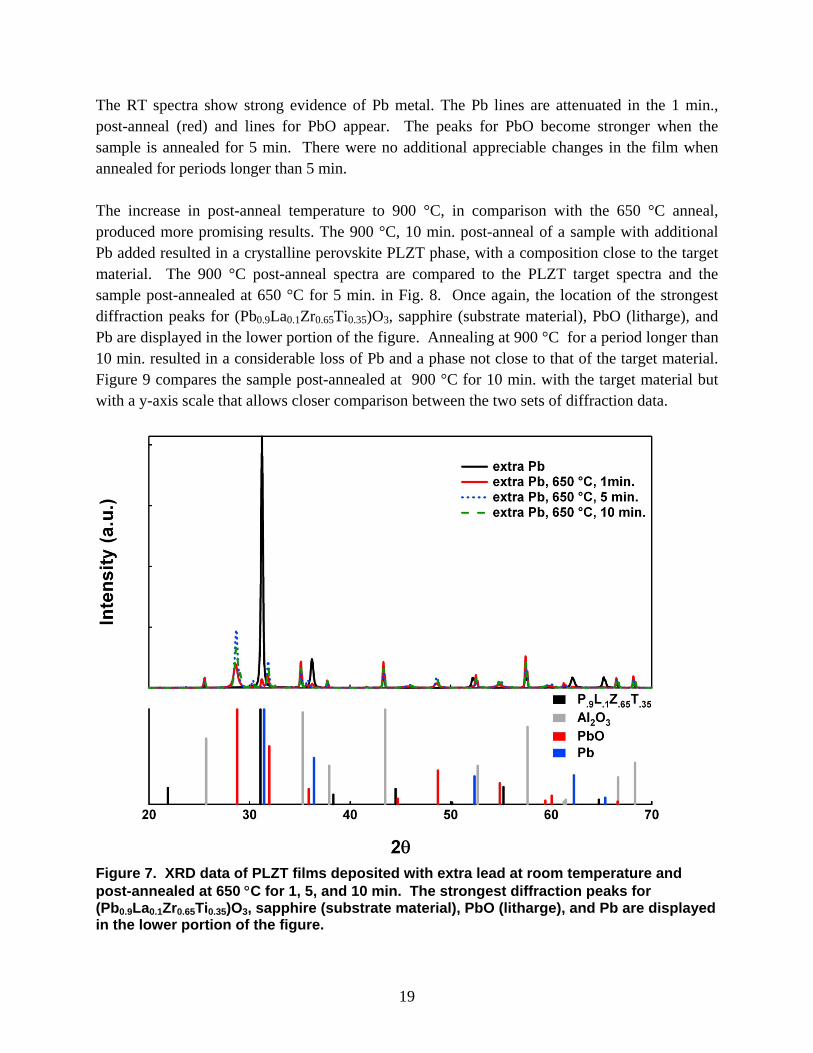
Figure 6. PLZT target (left) with Pb target (right) We made a second deposition using this composite PLZT-Pb target. The RHEPP-1 nitrogen beam was used for 60 pulses (RHEPP TJR28228 to TJR28289). Since oven post-anneal was the only heat treatment method we chose to continue investigating, only room temperature films were deposited. One sample was then oven post-annealed at 650 °C for 1 minute, a second sample was annealed at 900 °C for 10 minutes, and a third at 1100 °C for 10 minutes. Next, the 650 °C sample was annealed for an additional periods of time (5 min., 10 min., 1hr.), and examined by XRD after each anneal time increase. The XRD spectra from the RT deposition along with 1, 5, and 10 min. post-anneal at 650 °C are shown in Fig. 7. The location of the strongest diffraction peaks for Pb0.9La0.1Zr0.65Ti0.35)O3, sapphire (substrate material), PbO (litharge), and Pb are displayed in the lower portion of Fig. 7.
18
The RT spectra show strong evidence of Pb metal. The Pb lines are attenuated in the 1 min., post-anneal (red) and lines for PbO appear. The peaks for PbO become stronger when the sample is annealed for 5 min. There were no additional appreciable changes in the film when annealed for periods longer than 5 min. The increase in post-anneal temperature to 900 °C, in comparison with the 650 °C anneal, produced more promising results. The 900 °C, 10 min. post-anneal of a sample with additional Pb added resulted in a crystalline perovskite PLZT phase, with a composition close to the target material. The 900 °C post-anneal spectra are compared to the PLZT target spectra and the sample post-annealed at 650 °C for 5 min. in Fig. 8. Once again, the location of the strongest diffraction peaks for (Pb0.9La0.1Zr0.65Ti0.35)O3, sapphire (substrate material), PbO (litharge), and Pb are displayed in the lower portion of the figure. Annealing at 900 °C for a period longer than 10 min. resulted in a considerable loss of Pb and a phase not close to that of the target material. Figure 9 compares the sample post-annealed at 900 °C for 10 min. with the target material but with a y-axis scale that allows closer comparison between the two sets of diffraction data.
Figure 7. XRD data of PLZT films deposited with extra lead at room temperature and post-annealed at 650 °C for 1, 5, and 10 min. The strongest diffraction peaks for (Pb0.9La0.1Zr0.65Ti0.35)O3, sapphire (substrate material), PbO (litharge), and Pb are displayed in the lower portion of the figure.
19
Figure 8. XRD patterns for PLZT films deposited with extra lead and annealed at 900 °C for 10 and 30 min. and compared to the target material and a film annealed at 650 °C for 5 min.
Figure 9. Comparison of film post-annealed at 900°C for 10 min. with the PLZT target.
20
This shows that raising the temperature to 900 °C is necessary to fully transition the material to a perovskite PLZT phase. This does not necessarily mean that removal from vacuum and post-annealing in an external oven is necessary. The in-vacuum heater setup used here was not capable of reaching such a high temperature. It may be that a different setup using in-situ 900 °C annealing during the deposition might be as promising. The indication that 900 °C heating is required has significant implications for the manufacturing process. Such a high temperature excludes the use of many substrates, including all plastics. It is also evident that post-anneal after assembly of all the filler and electrode layers is likely to be problematic. This is because differential thermal expansion rates for the various layers likely would lead to distortion of the layer geometry and intra-layer stress as the filler material undergoes phase transformations during the heating. Lead volatility also becomes a serious issue at 900 °C. However, 900 °C is still considerably less than the 1100 °C sintering temperatures often required for tape-casted thick films of PLZT. 3.3. Multilayer Device Fabrication and Characterization We fabricated a multilayer capacitor device, in which successive dielectric and electrode layers were deposited and followed by a post-anneal at 900 °C. This was expected to be a challenging set of conditions for the performance of the final device. In addition to the layer distortions described above, which may be introduced by the post-heating process, the masking required to produce the electrode and filler layers may compromise the electrical properties of the capacitor. To understand this, imagine that the first electrode is deposited on the sapphire substrate. The first PLZT/Pb filler layer is then deposited on top of this layer. But, the boundary of the PLZT/Pb layer extends beyond the edge of the Rh electrode. Viewed from the side, as the filler layer approaches the Rh electrode edge, the filler material must ‘drop down’ onto the substrate a distance equal to the Rh electrode layer beneath it. This is illustrated in Fig. 10 (The individual layer heights have been exaggerated in this conceptual side drawing.) The first Rh electrode layer is shown in dark blue. The first PLZT/Pb layer (orange) extends beyond the Rh left-hand edge. The ‘drop down’ is indicated by the orange step. Then, the second Rh electrode layer (light blue) extends beyond the PLZT/Pb layer to its left. That layer is separated into 3 step heights. Since the PIBD layer deposition process is line-of-sight, there may be insufficient material to ‘bridge’ the step, and thus the light blue Rh may short to the dark blue layer when voltage is applied. In addition, there may be separate edge effects at each separate layer boundary that can distort fields and lead to shorting.
21
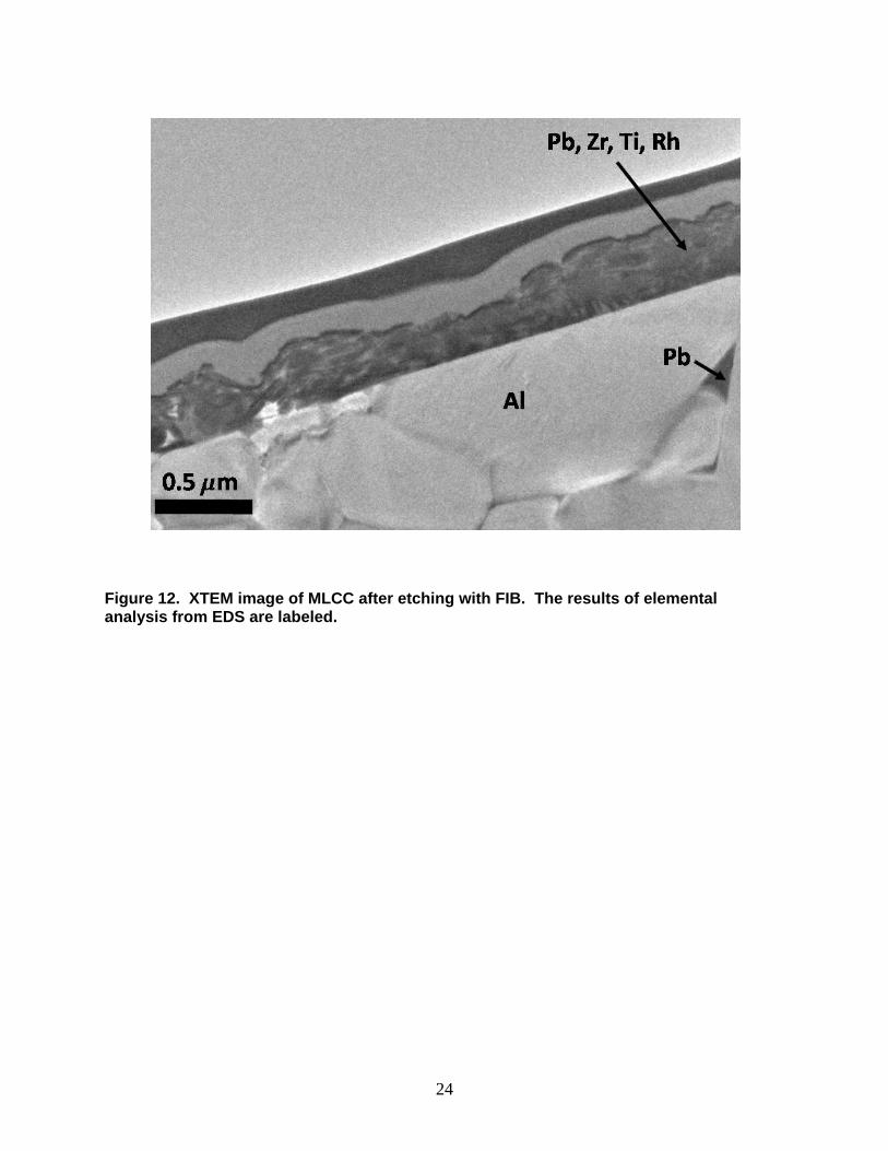
Figure 10. Diagram of successive layers of deposited electrode and dielectric material. A MLCC was constructed using this masking technique. A total of 71 layers (ion beam pulses) were deposited, followed by a oven post-anneal at 900 °C for 10 min. The device was shown to be shorted during electrical testing. Examination of the failed multilayer device after removing material using a focused ion beam (FIB) and imaging using scanning electron microscopy (SEM) revealed a very rough device surface. Some of the rough surface features extend very deep into the multilayer structure and could very easily disrupt the integrity of individual layers and device performance. A SEM image of the MLCC device etched using FIB is displayed in Figure 11. A XTEM image labeled with the elemental analysis from EDS is displayed in Figure 12. First, it is clear the Pb metal diffused throughout the device and was detected in the sapphire substrate, Ti adhesion layer, and mixed with the first Rh electrode. Second, the XTEM image does not reveal a discrete Ti adhesion layer or bottom Rh electrode. Instead, a mixture of Ti, Rh, Pb, and Zr is detected just above the substrate. Additionally, this mixed layer is full of voids, and shows signs of both individual layer breakup and delamination. The commixing of device layers and diffusion of conductive Pb metal could certainly be the cause of poor device performance. In order to more thoroughly understand the mechanical structure of the ion beam deposited film, single layer capacitors were fabricated without the post-anneal step. The purpose here was not to construct a successful device, as we have previously demonstrated that both extra added Pb and 900°C post-anneal were required to activate the PLZT layer. Rather, the purpose was to see if the deposited layer could maintain mechanical integrity, e.g. good discrete layer formation, good intra-layer adhesion without evident voids, etc. In a similar fashion to the multilayer capacitors, the single layer devices were etched using FIB and examined using both cross-sectional transmission electron microscopy (XTEM) and energy dispersive X-ray spectroscopy (EDS). An XTEM image of the single layer capacitor is shown in Fig. 13. An intial Rh layer was deposited, followed by a PLZT layer, and capped by a top Rh layer. These layers can be discerned in Fig. 13, although the captions are only approximate due to the thinness of the layers and the limits in resolution of the EDS process. (The Pt overcoat is deposited as part of the XTEM preparation process.) Thus the deposition process itself appears to result in a mechanically successful layer, provided the post-anneal heating is not applied. These devices were also shown to be shorted during electrical testing. But this is probably due as much to the masking process described above (Fig. 10). A more sophisticated masking procedure will probably be required in order to obtain enough voltage standoff to avoid device shorting.
22
Figure 11. SEM image of MLCC after etching with FIB.
23
Figure 12. XTEM image of MLCC after etching with FIB. The results of elemental analysis from EDS are labeled.
24
Figure 13. XTEM image of MLCC after etching with FIB. The results of elemental analysis from EDS are labeled.
4. DISCUSSION AND CONCLUSIONS The goal of this project was to investigate the feasibility of constructing MLCCs that exhibit high energy densities. The approach was to form a number of very thin dielectric layers that due to their geometric construction, show increased energy storage density. The layers were formed by ablation and redeposition of target materials using the RHEPP-1 pulsed intense ion beam. It was found that the PLZT target must be augmented with additional Pb, and the resulting films must be subjected to a high post-anneal temperature to form crystalline PLZT with the proper stoichiometry. Attempts at multilayer construction via RHEPP-1 deposition and an oven post-anneal at 900 °C resulted in a immediate device failure. Although PLZT films with an adequate stoichiometry and crystalline structure were achieved, both single and multilayer devices formed via ion beam deposition and a 900 °C post-anneal revealed a number of issues including extensive diffusion of Pb metal, layer mixing, layer delamination, and a roughened surface. The single-layer capacitor deposition suggests that a great deal of this can be ascribed to the high post-anneal temperature needed to activate the PLZT. The various layers, once deposited, can be expected to exhibit different coefficients of
25
thermal expansion (CTE), leading to significant intra-layer stresses upon high temperature annealing. It may be that in-situ heating to 900 °C could be used to form the multilayers, and that because the heating would be done during deposition, a temperature lower than 900°C may prove successful. In-situ deposition would probably lower the CTE stresses between the various layers. We know that a temperature higher than 450°C is required, and such a temperature is not possible in the RHEPP-1 vacuum tank, which contains diode hardware formed from plastic which could not withstand such temperatures. In this case, successful capacitor manufacture may require a new dedicated facility. In any case, further study is required to determine the relative importance of the issues discussed above, and to correct them to achieve viable capacitors.
26
5. REFERENCES 1. T. J. Renk, P. P. Provencio, S. V. Prasad, A. S. Shlapakovski, A. V. Petrov, K. Yatsui, W.
Jiang, and H. Suematsu, Materials Modification Using Intense Ion Beams, Proc. Of the IEEE 92, 1057-1081 (2004).
2. www.novacap.com 3. K. Yatsui, X. D. Kang, T. Sonegawa, T. Matsuoka, K. Masugata, Y. Shimotori, T. Satoh, S.
Furuuchi, Y. Ohuchi, T. Takeshita, and H. Yamamoto, Applications of intense pulsed ion beam to materials science, Phys. Plasmas 1, no. 5, 1730–1737, May 1994.
4. Y. Fudamoto, T. J. Renk, G. A. Torres, N. Kishimoto, Superconductivity in MgB2 films synthesized by ablation from high-power ion beam, Nucl. Instr. Meth. B – Beam Interactions with Materials & Atoms 250, 320-323 (2006).
5. Timothy J. Renk, Anatoli Shlapakovski, Robert R. Peterson, James P. Blanchard and Carl Martin, Minoconference on use of ion beams for surface modification, new materials synthesis, and materials response, Physics of Plasmas 12, 058302 (2005).
6. Timothy J. Renk, Paula P. Provencio, Paul G. Clem, Somuri Prasad, and Michael O. Thompson, Use of Intense Ion Beams for Surface Modification and Creation of New Materials, SAND2002-4215, printed December 2002.
7. Timothy J. Renk, Paula P. Provencio, S. V. Prasad, T. E. Buchheit, V. Engelko, D. McNulty, T. D. Petersen, and D. W. Petersen, Investigation of the Effects of Intense Pulsed Particle Beams on the Durability of Metal-to-Plastic Interfaces, SAND2005-1080, printed February 2005.
27
28
29
DISTRIBUTION 1 MS0899 Technical Library Org. 9536 (electronic copy) 1 MS0123 D. Chavez, LDRD Office Org. 1011 (electronic copy) 1 MS1415 Dave Sandison Org. 1110 (electronic copy) 1 MS1415 Elshan Akhadov Org. 1112 (electronic copy) 1 MS1415 Diane E. Peebles Org. 1112 (electronic copy) 1 MS1415 Todd Monson Org. 1112 (electronic copy) 1 MS1182 Timothy J. Renk Org. 5445 (electronic copy) 1 MS1182 Ronald J. Kaye Org. 5445 (electronic copy) 1 MS1182 Bob N. Turman Org. 5440 (electronic copy) 1 MS1164 William Guyton Org. 5400 (electronic copy) 1 MS1181 Larry X. Schneider Org. 1650 (electronic copy)