4 th Asian Forum for Accelerators and Detectors(AFAD’13), Feb. 25-26, Novosibirsk, Russia Ultrafast electron diffraction and microscopy using femtosecond RF gun Jinfeng Yang Osaka University, Japan
Transcript
4th Asian Forum for Accelerators and Detectors(AFAD’13), Feb. 25-26, Novosibirsk, Russia
Ultrafast electron diffraction and microscopy using femtosecond RF gun
Jinfeng Yang
Osaka University, Japan
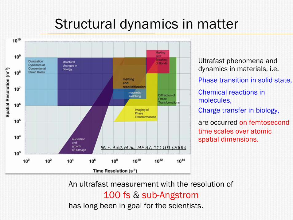
W. E. King, et al., JAP 97, 111101 (2005)
Structural dynamics in matter
An ultrafast measurement with the resolution of 100 fs & sub-Angstrom
has long been in goal for the scientists.
Ultrafast phenomena and dynamics in materials, i.e.
Phase transition in solid state,
Chemical reactions in molecules,Charge transfer in biology,
are occurred on femtosecond time scales over atomic spatial dimensions.
1) Ultrafast X-ray diffraction/image
Picosecond X-ray pulses from SR & femtosecond X-ray pulses from FEL or laserplasmas acceleration have been used.
→ big experiment/measurement,large energy deposited → large damage to samples.
2) Ultrafast electron diffraction (UED)
A fs laser pulse is used as pump, while a fs or ps e- bunch is used as probe.Almost UED facilities use keV DC electron DC guns. Very compact!Recently, the time resolution has been achieved to 100 fs using RF gun.
but no spatial resolution!
3) Ultrafast electron microscopy (UEM)
UEM can observe the dynamics of structural transformation in nanometer (evenatomic) spatial dimensions.
⇒ The resolution of UEM has achieved to 10 ns and 10 nm!
Ultrafast detection techniquesfor study of ultrafast phenomena and dynamics
Principle of ultrafast electron microscopy
: short electron pulse as probe
: short laser pulse as pump
Combination of pump-probe measurement with electron microscopy technique!
Δt=0
Δt>0
Δt = tl - te <0
Electron images Electron images at different timeat different time
Δt=0
W. E. King, et al., JAP 97, 111101(2005)
UEM
Short e- pulse
Phenomena & dynamics
Recent UEMs
•electron bunches with ~10 ns at 108 e-s/pulse•beam energy of ~100keV
(limited by the max. DC field:~10 MV/m)
photocathode DC gun in UEMs
Resolution in UEM is limited to10 ns & 10 nm(B. W. Reed, Workshop on UESDM, 2012)
λ= 211nm10 ns(FWHM)
λ= 1064 or 355nm12 ns FWHM
108 e-/bunch
e-s
B. W. Reed, Workshop on UESDM, 2012Problem using DC gun: Strong space-charge
force in low-energy e- bunch.Problem using DC gun: Strong space-charge
force in low-energy e- bunch.
Space-charge effect in recent UEM
Δt=300fs → 4ps during the 40cm transport of 30keV e- beam
B. J. Siwick et al., JAP 92, 1643(2002)
Bunch length increase due to space-charge force
mvrtNett0
22
2
0 2 επ+Δ≈Δ
1) Increase of bunch length during beam transport
2) Increase of energy spread during beam transport
ΔE/E→ 3x10⁻³ during the beam transport
1010--33
It is difficult to generate an fs electron beam in keV energy region!
⇒ The solution of the problems is to increase the beam energy!
⇒ The solution of the problems is to increase the beam energy!
Why use RF gun in UEM?
Can RF gun be used for UEM in fs time region?RF gun is a useful source in UED with fs time resolution!
A ~100 fs MeV electron bunch with 107-8 e-s/pulse
Resolution of 100 fs & 10 nm can be achieved?
What kind efforts and challenges are needed?
To answer the questions, we developed a prototype of time-resolved EM using RF gun.
photocathode DC gun
~keV electron bunches with ~10 ns
Single-shot imaging using 108 e-s/pulse
Resolution in UEMs: 10 ns & 10 nm
(B. W. Reed, Workshop on UESDM, 2012)
Recently, UEMs
a great technique for study of structural dynamics!
Recently, the RF gun has been successfully used/proposed in UED facilities at BNL, SLAC, UCLA, Tsinghua Univ. , Osaka Univ.,DESY, Shanghai Jiaotong Univ., KAERI, …
Space-charge effect is reduced!
RF gun based MeV UED at Osaka Univ.
Diffraction
ApertureΦ0.3mm
4.5x10⁷ e/pulse
Scintillator
EMCCD
RF gun
Probe 3ω:257nm,90fs,1kHz, 6mW
Pump 2ω:385nm,90fs, 10Hz, <40mJ/cm2
3MeV100 fs e‐ pulse
10Hz
apertureΦ0.3mm diffractionSi crystal
sample
P.Lens D.Lens
Probe 3ω
Pump 2ω(Φ600μm,
18.2o,p-pol )
1‐5MW@4μs,10Hz2856MHz
[1-10]
<10-8Pa
C.Lens Solenoid
Φ3.0mm
Φ300, 350μm
Sample
use of electron optical lenses as like in electron microscopy
Area: 5x5cmCsI (Tl) scintillator
Picture of UED system at Osaka Univ.
CCD
Probe laser
RF gun
CLDL
PLS
Pump laser
use of electron optical lenses, therefore, compact.
S.L
2.5 m
Single-shot measurement
1 shot (0.1s)
Si
single crystal SiThickness: 180nme‐ energy: 3MeV
Y. Murooka, et al., APL, 98, 251903 (2011)
1 shot (0.1s)
single crystal AuThickness: 15nme‐ energy: 3MeV
Au
A good-quality electron diffraction pattern can be observed with 105 e-s/bunch!
Laser heating and melting dynamics of single crystal Au
Prototype of Time-resolved MeV electron microscopy
Sol. lens
Cond. lens
Obj. lens
Proj. lens
Interm. lens
Prototype of MeV UEM in Osaka Univ.(height: 3m, diameter: 0.7m)
The prototype was constructed at the end of Oct. 2012.
Prototype of Time-resolved MeV electron microscopy
FemtosecondLaser
Femtosecondelectron beamFemtosecondelectron beam
Design of 2T objective lens
f0 = 5 mm for 2MeV e-
Cs (Cc) ~ 4 mm
70 cm (D) x 35 cm (H)
Thin Polymer mirror (5µm)ORCA-R2 CCD
•Illu. Vol.(<50µm)• Bright• High resol. (Column Structure)
• Tough (for High Eng. Xray)
• Large: 5x5cm2
CsI (Tl) scintillator (Hamamatsu)
X, e
MeV electron
Detection of MeV electron images
The detection system was successfully used in UED measurement.(single-shot measurement with 105 e-s/pulse)
Single-shot
10 pulses
MeV electron diffractions observed with 10 pulses and single-shot measurements
Electron beam (2.3 MeV)
diff. plane(BFP)
Imaging plane(Selector diaphragm)
Projectorlens
Objective Lens
Sample: Au single crystal, ~15 nmElectron charge: ~100 fC/pulse
Specimen
First MeV electron diffraction in UEM prototype
A goodA good--quality MeV ED was observed!quality MeV ED was observed!
SingleSingle--shot measurement is available!shot measurement is available!
21
Observed images of Au film
First MeV electron imaging in UEM prototype
Images of Au film
Observation #1
Exposure time:2s Exposure time:60s
X385 x650 x1200
x650 x1200
10μm
10μm
38nm/pixel
38nm/pixel
Observation #2
Electron beam (2.3 MeV)
Interm.image planeProjector
lens
Specimen
Final image screen
BFP(Obj. Aper.)
Objective Lens
Sample: Au single crystal, 15 nmElectrons at screen: ~10 fC/pulse 83μm
38 μm
x50
Magnifications & spatial resolution
Electron beam (~MeV)
BFP
Interm.image plane
(Obj. Aper.)
Projectorlens
Objective Lens
Sample: Cu grid, 1000 meshElectron charge: ~10 fC/pulse
Specimen
Final image screen
StandardCu grid
(1000mesh)
�測例① X650 x1700
5 μm 30 nm/pixel75 nm/pixel10μm
X200
σ~300nm
σ~300nm
25μm
5.5 μm
Femtosecondelectron beam
Objective lens
Specimen
Intermediate lens
Projector lens
CL-1
CL-2
Solenoid lens
RF gun
Spatial resolution300 nm (present)
10nm (next step)
<1nm (in future)
New science and technology using UEM
Structural observation and imaging in “real space” with atomic-scale spatial resolution using high-energy electron beam.
Imaging Technologyイメ�ジング テクノロジ�
Electron beam(1~3MeV)
Observations of fundamental dynamic processes in matter occurring on femto-second time scales over atomic spatial dimensions.
UltrafastObservation超高速現象の�察
Electron pulse(probe)
Pump laser pulse
Methods
TargetsProtein Structural Dynamicsタンパク質構造ダイナミクス
•Protein structural dynamics•Macromolecular structure•Reveal of functioning processes•New technologies and applications in medical biology.
Making Molecular Movie分子運動の可視化:-新しい科�-
•Observation of single molecule motion.•Ultrafast chemical reactions•Solvation dynamics•Discovery of transition states and reaction intermediates.
Nano-technology/scienceナノテクノロジ��サイエンス
•Transformation dynamics of novel nano-scale materials.•Creation of new functional materials and devices for nanotechnology.
Compact high-voltage electron microscopy(dream TEM)
Phase transitions
Novel ultrafast technique at atomic level(dream UEM)
Conclusion
However, great efforts and many challenges are required:
reduce further the emittance (<0.1 μm) and energy spread (10-5 or less),
increase the beam brightness,
improve the stabilities on the charge and energy,
develop a detection of very electron with MeV energy, and so on.
Both RF gun based UED and UEM systems have been constructed at Osaka University.
In UED, single-shot and time-resolved measurements have been succeeded.
In UEM, the MeV electron diffraction and imaging experiment was carried out.
Both experiments suggest that RF gun is very useful for ultrafast MeV electron diffraction and is also expected to be used in ultrafast electron microscopy.
Acknowledgments
Co-workers at Osaka University:N. Naruse, Y. Murooka, K. TanimuraK. Kan, T. Kondoh, Y. Yoshida
Collaborators:J. Urakawa(KEK), T. Takatomi(KEK), R. Kuroda(AIST)
25
Present work was supported by Grant-in-Aid for Scientific Research from JSPS!
10m
3m
Standard 3-MeV TEMat Osaka Univ.
Next TEM: “Dream TEM”
Compact High-VoltageTransmission Electron Microscopy


![Ultrafast transmission electron microscopy using a laser ...transmission electron microscopy [4], scanning electron microscopy [5], x-ray diffraction [6], scanning tunneling and atomic](https://static.documents.pub/doc/80x56/607eb1335ce8082131294459/ultrafast-transmission-electron-microscopy-using-a-laser-transmission-electron.jpg)


