ULTRAHIGH VACUUM SURFACE ANALYSIS STUDIES OF ELECTROCHEMICAL
ATOMIC LAYER DEPOSITION OF METALS AND COMPOUND SEMICONDUCTORS
by
JAY YU KIM
(Under the Direction of John Lewellen Stickney)
ABSTRACT
The main topic of this dissertation is electrochemical atomic layer deposition (ALD) by
ultrahigh vacuum (UHV) surface analysis. The purpose of electrochemical ALD is to form
smooth thin films at room temperature. The first part of this dissertation will be about platinum
(Pt) and copper (Cu) electrochemical ALD on gold (Au) substrate. The surface-limited redox
replacements (SLRR) were used in these cases. In case of forming a Pt atomic layer, a Cu atomic
layer, as a sacrificial layer, was first formed by underpotential deposition (UPD) on the clean and
annealed Au(111) single crystal. Then, it was immersed in the Pt solution at open circuit, and a
Cu atomic layer was replaced spontaneously by Pt ions, so a Pt atomic layer was formed on the
substrate. To form multiple Pt atomic layers, the subsequent Pt replacements with Cu sacrificial
layers were done on the substrate. In order to grow Cu atomic layers on the substrate, lead (Pb)
atomic layers were used as the sacrificial layers. I− and Cl− anions were used in solutions for
electrochemical annealing. Auger electron spectroscopy (AES), low-energy electron diffraction
(LEED), and scanning tunneling microscopy (STM) were performed to estimate the quality of
the thin films on the substrate.
The second part of this dissertation is about the electrochemical ALD on GaAs(100)
substrate. After the substrate was cleaned, an attempt was made to deposit a Te atomic layer on
the substrate. A Te atomic layer on the substrate is expected as a precursor to deposit metals,
such as cadmium (Cd) or indium (In). From the Auger ratios of In/Te and Te/Ga, the In2Te3
atomic layer was attempted to form on the substrate. The deposited In2Te3 thin film thickness
was calculated from the Auger electron spectra. The future plan with this GaAs(100) substrate is
to form atomic layers of InSb, Sb2Te3, and In2Sb2Te3.
INDEX WORDS: Electrochemical atomic layer deposition, Electrodeposition, Underpotential deposition, Ultrahigh vacuum, Surface-limited redox replacement, Auger electron spectra, Low-energy electron diffraction, Scanning tunneling microscopy, Metal, Compound semiconductor
ULTRAHIGH VACUUM SURFACE ANALYSIS STUDIES OF ELECTROCHEMICAL
ATOMIC LAYER DEPOSITION OF METALS AND COMPOUND SEMICONDUCTORS
by
JAY YU KIM
B.S., Korea University, Korea, 2000
M.S., Korea University, Korea, 2002
A Dissertation Submitted to the Graduate Faculty of The University of Georgia in Partial
Fulfillment of the Requirements for the Degree
DOCTOR OF PHILOSOPHY
ATHENS, GEORGIA
2008
ULTRAHIGH VACUUM SURFACE ANALYSIS STUDIES OF ELECTROCHEMICAL
ATOMIC LAYER DEPOSITION OF METALS AND COMPOUND SEMICONDUCTORS
by
JAY YU KIM
Major Professor: John L. Stickney
Committee: James L. Anderson I. Jonathan Amster
Electronic Version Approved:
Maureen Grasso Dean of the Graduate School The University of Georgia August 2008
v
ACKNOWLEDGEMENTS
First of all, I would like to thank my major professor, John L. Stickney. Since I became
his student four and a half years ago, he has always been encouraging me to be a scientist, and
not just to be a technician. I have been learning not only how to do science, but also how to
communicate with people, thanks to him. I would like to acknowledge and thank Professors
James Anderson and Jonathan Amster for serving on my committee and for their valuable advice.
I would like to thank my former laboratory members: Dr. Mkhulu (Ken) Mathe, Dr. Nattapong
(Nat) Srisook, Dr. Madhivanan (Madhi) Muthuvel, and Dr. Venkatram (Ram) Venkatasamy. I
would also like to express my gratitude to my present laboratory members: Dr. Youn-Geun Kim,
Nagarajan Jayaraju, Dhego Banga, Chandru Thambidurai, Daniel Gebregziabiher, Xuehai Liang,
and Leah Sheridan. I would like to thank and give my love to my parents, my parent-in-law, my
brother, my sister-in-law, my brother-in-law, and my lovely wife, Mee Kyung, for their supports,
advices, and prayers. Finally, I would like to thank and praise God for guiding my life to this
point.
“The LORD is my shepherd; I shall not be in want. He makes me lie down in green pastures,
he leads me beside quiet waters, and he restores my soul. He guides me in paths of
righteousness for his name’s sake. Even though I walk through the valley of the shadow of
death, I will fear no evil, for you are with me; your rod and your staff, they comfort me. You
prepare a table before me in the presence of my enemies. You anoint my head with oil; my cup
overflows. Surely goodness and love will follow me all the days of my life, and I will dwell in
the house of the LORD forever.” (Psalm 23:1~6)
vi
TABLE OF CONTENTS
Page
ACKNOWLEDGEMENTS.............................................................................................................v
CHAPTER
1 INTRODUCTION AND LITERATURE REVIEW.....................................................1
2 STUDIES OF CU ATOMIC LAYER REPLACEMENT, FORMED BY
UNDERPOTENTIAL DEPOSITS, TO FORM PT NANOFILMS USING
ELECTROCHEMICAL ATMOIC LAYER EPITAXY (EC-
ALE)......................................................................................................................25
3 COPPER NANOFILM FORMATION BY ELECTROCHEMICAL ATOMIC
LAYER DEPOSITION (ALD) : UHV-EC AND IN-SITU STM STUDIES........40
4 CU NANOFILM FORMATION BY ELECTROCHEMICAL ATOMIC LAYER
DEPOSITION (ALD) IN THE PRESENCE OF CHLORIDE IONS...................69
5 SURFACE STRUCTURES OF CLEAN N-GE(111) AND N-GAAS(100)
SUBSTRATES : UHV-EC AND IN-SITU EC-STM STUDIES..........................97
6 ULTRAHIGH VACUUM SURFACE STUDIES OF THE ELECTROCHEMICAL
ATOMIC LAYER DEPOSITION OF INDIUM TELLURIDE ON N-TYPE
GAAS(100)...........................................................................................................133
7 ELECTROCHEMICAL ATOMIC LAYER DEPOSITION (ALD) OF INDIUM
ANTIMONIDE ON N-TYPE GAAS(100)...........................................................160
8 CONCLUSION AND FUTURE STUDIES..............................................................178
2
Introduction
In principle, there are three basic types of thin film growth: island or Volmer-Weber
growth, layer or Frank-van der Merwe growth, and island-layer or Stranski-Krastonov growth [1-
4]. Island growth occurs when the growth species are more strongly bonded to each other than to
the substrate. Many systems of metals on insulator substrates, alkali halides, graphite, and mica
substrates display this type of nucleation during the initial film deposition. Subsequent growth
results in coalescence of the islands to form a continuous film. The layer growth is the opposite
of the island growth, where growth species are equally bound more strongly to the substrate than
to each other. A first complete monolayer is formed, before the deposition of a second layer
occurs. Providing the decrease in bonding energy is continuous toward the bulk-crystal value, the
layer growth mode is sustained. The most important examples of layer growth mode are the
epitaxial growth of single crystal films. The island-layer growth is an intermediate combination
of layer growth and island growth. In this case, after forming one or more monolayers,
subsequent layer growth becomes unfavorable and islands form. Such a growth mode typically
involves stress, which is developed during the formation of the nuclei or films. This growth is
fairly common and has been observed in metal-metal and metal-semiconductor systems.
Layer-by-layer growth of thin films has been more desirable and applicable in many
electronic industries than island growth because of the high crystallinity, low resistance, and
continuous characterization of the films [5, 6]. Fundamental to forming high quality structures
and devices with thin films of metal and semiconductors is the concept of epitaxy. The epitaxy
focuses on the formation of single crystal films on single crystal substrates [7]. Epitaxial
deposition with molecular beam epitaxy (MBE) or vapor phase epitaxy (VPE) involves mass
transport to and diffusion along the surface. It is generally better to deposit slowly, and to use
3
higher temperatures, limiting the number of atoms depositing at a given time, and allowing their
diffusion to optimal sites, for instance at step edges, to promote epitaxy.
Electrochemical atomic layer epitaxy (ALE) or atomic layer deposition (ALD) has been
studied for many years to produce high quality thin films [7]. ALE or ALD is a methodology
used initially to improve epitaxy in the growth of thin films by MBE or VPE. The principle of
ALE or ALD is to use surface-limited reactions to form each atomic layer of a deposit. If no
more than an atomic layer is ever deposited, the growth will be two-dimensional (2-D), layer-by-
layer. Surface-limited reactions are developed for the deposition of each component element, and
a cycle is formed with them. With each cycle, a compound monolayer is formed, and the deposit
thickness is controlled by the number of cycles.
Surface-limited reactions are generally referred to as underpotential deposition (UPD) [7,
8]. UPD is the phenomenon that, in the deposition of one element on a second, frequently the
first element will form an atomic layer at a potential prior to, under, that needed to deposit the
element on itself. One way of looking at UPD is that a surface compound, or alloy, is formed,
and the shift in potential results from the free energy of formation of the surface compound.
Electrochemical ALD is the combination of UPD and ALD. Atomic layers of component
elements are deposited at underpotentials in a cycle, to directly form a compound. It is layer-by-
layer growth, avoiding three-dimensional (3-D) nucleation, and offering increased degrees of
freedom, atomic level control, and promoting of epitaxy. It also offers a way of better
understanding compound electrodeposition, a way of breaking it down into its component pieces
[7]. It allows compound electrodeposition to be deconvolved into a series of individually
controllable steps, resulting in an opportunity to learn more about the mechanisms, and gain a
series of new control points for electrodeposition. In this process, each reactant has its own
4
solution and deposition potential, and there are generally rinse solutions as well. Each solution
can be separately optimized, so that the pH, electrolyte, and additives or complexing agents are
tailored to fit the precursor. Finally, electrochemical ALD involves growth in a condensed phase
with potential control instead of thermal. This increases the variable space for producing
materials; the diversity of conditions under which compounds can be formed.
This dissertation mainly focuses on electrochemical ALD of metal and compound
semiconductor thin films on Au(111) and n-type GaAs(100) substrates. Chapter 2 first introduces
a novel technique to grow smooth Pt thin film in layer-by-layer mode on Au(111) substrate, by
surface-limited redox reaction (SLRR). A Cu atomic layer was used as a sacrificial layer in this
Chapter. In Chapter 3, the surfaces of the Cu thin film grown on Au(111) substrate, up to 10
replacement cycles, by SLRR with Pb sacrificial layers, are characterized with Auger electron
spectra (AES), low-energy electron diffraction (LEED), and in-situ electrochemical scanning
tunneling microscopy (EC-STM). In this Chapter, iodine (I) is used for the electrochemical
annealing of both substrate and Cu film. In Chapter 4, chlorine (Cl) is used for the
electrochemical annealing, and its effects on Cu SLRR are studied. In Chapter 5, semiconductor
substrates, n-type Ge(111) and n-type GaAs(100), are cleaned and annealed. Their reconstructed
surface structures are studied by LEED and EC-STM. Chapter 6 introduces the first attempt to
electrodeposit a Te atomic layer on n-GaAs(100). Electrodeposition of an indium (In) atomic
layer on a Te atomic layer on n-GaAs(100) is attempted in this Chapter. An In-Te thin film is
then electrodeposited up to thee cycles. In Chapter 7, indium antimonide (InSb) thin film was
deposited on n-GaAs(100) by electrochemical ALD. Last but not least, in Chapter 8, the
conclusions are drawn and the future studies are presented.
5
Literature Review
In the Stickney lab, EC-ALE has been intensively studied for 20 years. EC-ALE is an
electrochemical analog to ALE [7]. Their early works involved the electrochemical and surface
analysis of HCl adsorbed on tri-phase Cu electrodes [9-11]. Compound semiconductors have
been formed by EC-ALE on Au substrates; including II-VI compounds such as CdS [12], CdSe
[12-14], CdTe [12, 15-21], ZnS [22], ZnSe [22], ZnTe [22], HgSe [23, 24], HgTe [25], and
recently MCT (HgxCd(1−x)Te) [26], IV-VI compounds such as PbSe [27, 28] and PbTe [28], and
III-V compounds such as GaAs [29, 30], InAs [31], and InSb [32]. Recently, electrochemical
ALD of compound semiconductor thin films of GeTe and GeSb on Au(111) with flow cell
system [7, 22] is under study in this laboratory. Several other groups have been using EC-ALE to
grow compound semiconductors on various metal substrates, such as CdS on Au(111) [33],
Sb2Te3 and Bi2Te3 on both Au(111) and Pt(111) [34-36], and CdS, ZnS, ZnSe, and InAs on
Ag(111) [37-39].
2-D electrochemical epitaxial growth of single-crystal metal thin films has been a
difficult task. In general, metals grow as 3-D clusters on the substrate, which can cause difficult
analysis of the surface because of their non-uniform coverage of the substrate. It is reported that
the 3-D cluster problems can be solved by the replacement of desirable metals by Cu or Pb UPD
phenomenon [40-43]. Sieradzki et al. developed an electrochemical technique that serves to
significantly enhance ambient-temperature nucleation 2-D islands, called defect-mediated
growth (DMG) [41]. The mediator was periodically deposited and stripped from the surface by
appropriate cycling of the electrochemical potential. A monolayer (ML) was completed as the
growing 2-D clusters eventually merge. Adzic et al. proposed that the UPD adlayer is oxidized
by the more noble metal cations, which are simultaneously reduced and deposited on the gold
6
substrate, and this can be expressed as: M0UPD + (m/z) Pz+ → Mm+ + (m/z) P0, where M0
UPD
represents a UPD metal adatom on the electrode surface S and Pz+ is a noble metal cation with
positive charge z+ and valence z [42]. They reported that an interesting novel procedure of near-
uniform Pd ML on Au(111) could be formed by the spontaneous redox replacement of a
previously prepared Cu UPD layer by Pd (II) solute, confirmed by STM [42]. Figure 1.1 shows
the cartoon of Pt surface-limited redox replacement (SLRR) with a Cu sacrificial UPD layer.
However, in case of Pt (IV) replacement, a submonolayer of Pt was formed because of the
stoichiometry: 2Cu0UPD + Pt4+ → 2Cu2+ + Pt0. Weaver et al. reported the preparation of Pt-group
metal films on roughened gold electrodes by utilizing spontaneous redox replacement of a Cu or
Pb UPD with a Pt-group metal cation solute, and the resulting films displayed intense surface-
enhanced Raman scattering (SERS) for adsorbates bound to the overlayer and free from substrate
interferences [43]. Stickney et al. recently have made some progress in the atomic scale studies
of Pt [44, 45] and Cu [46-48] thin films, grown a couple of replacement cycles by SLRR on
Au(111) single crystal. AES, LEED, and in-situ EC-STM were used to characterize the surfaces
of thin films. Iodine and chlorine were used for the electrochemical annealing to modify the
surface. Up to date, several attempts have been made in their laboratory to grow smooth and
thicker films, 10 ~ 20 nm or thicker, of Pt, Cu, and Ru, by SLRR and flow cell system. The
surfaces of these films are characterized by electron probe microanalysis (EPMA) and X-ray
diffraction (XRD).
Gallium arsenide (GaAs) is an important III-V compound semiconductor nowadays, and
it is substantially replacing the Si substrate in electronic industries because of their higher
crystallinity and large mobility [49]. Growing another compound semiconductor on GaAs
substrate would be applied to optoelectronic, thermoelectronic, and photovoltaic devices. Several
7
groups have been attempting to grow chalcogen atomic layers (S, Se and Te) as a passivating
layer, by MBE, on GaAs substrates [50-55]. A chalcogen passivating layer on the substrate can
also be used as a precursor layer for a metal (such as Cd [56-59], Zn [60, 61], In [62], or Sb [63])
atomic layer, grown by MBE. There have been a number of electrodeposition studies where
GaAs was used as a substrate; however, atomic level studies of GaAs surfaces in electrochemical
environments have been few. Etcheberry et al. electrodeposited CdSe on InP (100), GaAs(100),
and GaAs(111) [64-67]. They co-deposited CdSe from a single solution, at a couple of different
potentials on the substrates, and analyzed the surface with XRD, X-ray photoelectron
spectroscopy (XPS), LEED, and reflection high-energy electron diffraction (RHEED). Allongue
et al. electrodeposited metals such as Pt, Pd, Ni, Co, Cu, and Ag, on n-GaAs(100), from separate
solutions, without the use of any passivation layer [68-71]. Recently, Kim and Stickney first
attempted to electrodeposit a Te atomic layer on n-type GaAs(100) substrate and to
electrodeposit an indium (In) atomic layer on a Te layer to form In2Te3 compound, characterized
by AES [72]. In addition, we performed three subsequent In-Te ALD cycles on the substrate.
The detail of this study is described in Chapter 6.
Experimental Procedure
Cleaning the Substrate
Prior to deposition, the substrates must be clean, which means no oxide or carbon should
be formed on the substrates. To clean the gold substrate, it is immersed in hot concentrated nitric
acid for about 30 minutes and then annealed in a hydrogen flame for about 10 minutes [73]. Then,
the gold substrate can be cleaned by Ar+ ion bombardment in the ultrahigh vacuum (UHV)
chamber [20, 74]. Figures 1.2 and 1.3 show the schematic diagrams of the UHV chamber and
8
Ar+ ion bombardment, respectively. The cryopump and ion pump are attached to the main
chamber so that the UHV state (~ 10−9 Torr) can be reached. The sorption pumps (roughing
pumps) are attached to the chamber, which are not shown in Figure 1.2. For the Ar+ ion
bombardment to clean substrates, an Ar gas line is connected to the main chamber. When Ar gas
is purged into the chamber and the gas molecules are hit by electrons from the electron gun (~ 1
keV of Ar+ ions with a current density of ~ 2.5 µA), the gas molecules would be ionized, the Ar+
ions would sputter the grounded substrate, and the impurities would be removed. However, the
surface after the ion bombardment would be rough, and it would be hard to see a LEED pattern;
therefore, the substrate needs to be annealed [20, 74]. The annealing can be performed, simply
by connecting the substrate with tungsten wire and applying some current to the wire.
Electrochemistry in the ante-chamber
Electrochemistry can be done in the ante-chamber attached to the main chamber (Figure
1.2). The electrochemical cell container is attached to the ante-chamber with a gate valve and
each solution is filled in the electrochemical cell and drained to the waste bottle after
electrodeposition. All solutions were deaerated with ultrahigh purity (UHP) (99.998 %) Ar gas
for at least 30 minutes prior to each experiment. Figure 1.4 shows the substrate holder and the
electrochemical cell in the ante-chamber. In the electrochemical cell, there are a working
electrode (the substrate), a Ag/AgCl reference electrode (3 M KCl, Bioanalytical System, Inc.),
and a gold wire auxiliary electrode, connected to a potentiostat. Before immersing the substrate
in a solution, the ante-chamber is back-filled with UHP Ar gas. After immersing, cyclic
voltammograms (CV) are obtained by scanning potential with 5 mV/second scan rate. The
coverage of adsorbate on the substrate can be obtained by calculating the ratio of [the charge (in
µC) of the adsorbate by integrating UPD peak] to [the theoretical charge (in µC) of the adsorbate
9
to form a monolayer (ML)] [75]. By definition, one ML indicates one adsorbate for each surface
atom [7]. After the electrodeposition, the substrate is emersed (withdrawn) from the solution.
Upon emersion, the double-layer would lose electrical contact with the bulk electrolyte, but not
with the electrode [74]. Thus, the overall charge within the interface must remain neutral.
However, this requirement for neutrality would allow the occurrence of spontaneous faradaic
reactions within the emersed layer. Such reactions can take place spontaneously provided that
they do not result in charge imbalance within the layer, even if they are accompanied by loss of
adsorbate [74]. If the solutions constantly flow through the cell, one solution can be exchanged
with the next solution without losing potential control [7, 22]. Therefore, the flow cell system in
the ante-chamber is currently under construction.
Then, the ante-chamber should be evacuated in order to transfer the substrate to the main
chamber for surface analysis. Upon evacuation, there may be precipitates or salts formed on the
surface if the solution concentration is too high, or possible surface perturbation or
reconstruction may be occurred [74, 75]. To prevent the problems, the solution concentration
should as low as ~ mM. After evacuating the ante-chamber, the substrate is transferred from the
ante-chamber to the main chamber through a gate valve, without exposing to air, so there would
be the least chance for the surface to be oxidized. The surface is then characterized by AES,
LEED, and XPS (under construction).
Ultrahigh Vacuum Surface Analysis
The surface analysis requires UHV condition because the electrons ejected from an
electron gun should reach at the surface without colliding with gas molecules [76, 77]. Also,
UHV prevents the surface from being oxidized and contaminated. The following surface analysis
techniques have been used in Stickney’s laboratory.
10
- Auger Electron Spectroscopy (AES): The surface to be analyzed is irradiated with a beam of
electrons of sufficient energy, typically in the range of 2-10 keV, to ionize one or more core
levels in surface atoms [5, 6, 74, 75, 77]. In Figure 1.5, after the ionization, the atom can be
relaxed by either of the two processes, ejection of a characteristic X-ray photon (fluorescence)
or ejection of an Auger electron. The resulting ejected Auger electron has a kinetic energy
given by: Ekin (KL1L23) = EK − EL1 − EL23 − Einter (L1L23) + ER − ΦS, where Einter (L1L23) is the
interaction energy between the holes in the L1 and L23 shell, ER is the sum of the intra-atomic
and extra-atomic relaxation energies, and ΦS is the work function term. Because no two
elements have the same set of atomic binding energies, analysis of Auger energies provides
elemental identification.
- Low-Energy Electron Diffraction (LEED): Figure 1.6 shows the schematic diagram of LEED
[5, 6, 74, 75, 77]. The incident electron beam, accelerated by the potential V0, is emitted from
the electron gun behind the hemispherical fluorescent glass screen and hits the sample through
a hole in the screen. The surface is at the center of the hemisphere so that all back-diffracted
electrons travel towards the LEED screen on radial trajectories. Before the electrons hit the
screen, they must pass a retarding field energy analyzer, which typically consists of four (or
three) hemispherical grids concentric with the screen, each containing a central hole through
which the electron gun is inserted. The first grid is connected to the earth ground, and it
minimizes undesirable electrostatic deflection of diffracted electrons. The second and third
(only second) grids is called suppressor grids, which enable a narrow energy range of
elastically scattered electrons to be transmitted to the fluorescent screen. The fourth (third) grid
is usually grounded to reduce field penetration of the suppressor grids by the screen voltage to
make the diffraction spots visible. Because the fluorescent screen is transparent, the spots can
11
be observed through a viewport behind the screen without being shadowed by the sample
holder. Only the electron gun assembly (diameter < 15 mm) obstructs the view slightly. The
usual way of recording the LEED pattern is a light-sensitive digital camera.
- In-situ Electrochemical Scanning Tunneling Microscopy (EC-STM): STM is a fascinating
technique for atomic scale surface morphologies. In STM, the probe is a sharp metal tip
scanned across a conducting surface at distances of the order of typically 1 nm [6, 77]. A bias
voltage of typically a few mV is applied between the tip and the sample leading to a tunneling
current of the order of a few nA.
In the Stickney lab, in-situ EC-STM has been used for atomic scale surface
morphologies [45-48]. In-situ EC-STM is the combination of electrochemistry and STM, and
is opposed to ex-situ STM in air or vacuum. It is the technique in which the current that flows
through a very small electrode tip near a conductive, semiconductive, or even a insulating
substrate immersed in solution is used to characterized processes and structural features at the
substrates as the tip is moved near the surface [78]. Figure 1.7 shows the schematic diagram of
in-situ EC-STM. In EC-STM, the working electrode is mounted horizontally at the bottom of a
small cell that contains auxiliary and reference electrodes. The scanning tip is held above the
working electrode. The potentials of the working electrode (Ew) and the tip (Et) are controlled
independently with a potentiostat, where Ew is selected to produce the reaction of interest and
Et is adjusted to give the desired bias [78]. Because only the tunneling current is of interest in
EC-STM, electrode reactions that occur at the tip are undesirable. Thus, in EC-STM, the tip is
coated with glass or polymer, with only a very small area at the very bottom portion left
exposed [78]. The actual exposed area can be estimated, if necessary, by using the tip as an
ultramicroelectrode (UME), noting the magnitude of the limiting current in a known solution.
12
The tip potential is also chosen to be in a region where electrode reactions do not occur. The
thickness of the electrolyte layer over the working electrode must be small, so that only the tip,
and not the tip holder or a piezo, contacts the solution [78]. This arrangement makes it difficult
to keep the electrolyte solution free of oxygen, unless the whole cell and STM head are kept in
an inert atmosphere, such as with a glove bag.
The EC-STM tip interacts with the surface both by interatomic forces and by the tip’s
electrical field. Thus, the tip can affect the structure of the scanned area, especially at high
tunneling currents [78]. This effect can sometimes be recognized after scanning over a given
small region by decreasing the set tunneling current, increasing the x-y scan dimensions, and
observing whether an image of a square perturbed region, where the earlier scanning took place,
is visible [78].
An important limitation of EC-STM is that a quantitative correlation between the
tunneling current and useful theoretical equations is not yet possible [78]. Thus, there is little
real chemical and analytical information in the EC-STM scans, and one gains mechanistic and
structural information mainly from the interpretation of images. However, one can obtain
additional information by noting how the EC-STM behavior varies with the substrate potential
versus a reference electrode or the tip bias between tip and substrate [78].
References
1. G. Cao, Nanostructures & Nanomaterials, Imperial College Press, London, 2004.
2. M. Ohring, Materials Science of Thin Films, Academic Press, San Diego, 2002.
3. N. Kanani, Electroplating, Elsevier, Oxford, 2004.
4. M.A. Herman, W. Richter, and H. Sitter, Epitaxy, Springer, Berlin, 2004.
13
5. G.A. Somorjai, Chemistry in Two Dimensions: Surfaces, Cornell University Press, Ithaca,
1981.
6. G.A. Somorjai, Introduction to Surface Chemistry and Catalysis, John Wiley & Sons,
Inc., New York, 1994.
7. J.L. Stickney, in Advances in Electrochemical Science and Engineering, R.C. Alkire and
D.M. Kolb (Eds.), pp. 1 ~ 105, Wiley-VCH, Weinheim, 2002.
8. D.M. Kolb, M. Przasnyski, and H. Gerischer, J. Electroanal. Chem., 54, 25 (1974).
9. J.L. Stickney, C.B. Ehlers, and B.W. Gregory, in Electrochemical Surface Science, M.P.
Soriaga (Ed.), ACS Press, Washington, 1988.
10. J.L. Stickney, C.B. Ehlers, and B.W. Gregory, Langmuir, 4, 1368 (1988).
11. C.B. Ehlers, I. Villegas, and J.L. Stickney, J. Electroanal. Chem., 284, 403 (1990).
12. L.P. Colletti, B.H. Flowers Jr., and J.L. Stickney, J. Electrochem. Soc., 145, 1442 (1998).
13. T.E. Lister and J.L. Stickney, Appl. Surf. Sci., 107, 153 (1996).
14. M.K. Mathe, S.M. Cox, B.H. Flowers, R. Vaidyanathan, L. Pham, N. Srisook, U. Happek,
and J.L. Stickney, J. Cryst. Growth, 271, 55 (2004).
15. B.W. Gregory and J.L. Stickney, J. Electroanal. Chem., 300, 543 (1991).
16. D.W. Suggs and J.L. Stickney, Surf. Sci., 290, 362 (1993).
17. D.W. Suggs and J.L. Stickney, Surf. Sci., 290, 375 (1993).
18. L.B. Goetting, B.M. Huang, T.E. Lister, and J.L. Stickney, Electrochim. Acta, 40, 143
(1995).
19. H.M. Baoming, T.E. Lister, and J.L. Stickney, in Handbook of Surface Imaging and
Visualization, A.T. Hubbard (Ed.), CRC Press, Boca Raton, 1995.
14
20. K. Varazo, M.D. Lay, T.A. Sorenson, and J.L. Stickney, J. Electroanal. Chem., 522, 104
(2002).
21. B.H. Flowers Jr., T.L. Wade, J.W. Garvey, M. Lay, U. Happek, and J.L. Stickney, J.
Electroanal. Chem., 524-525, 273 (2002).
22. J.L. Stickney, in Electroanalytical Chemistry, A.J. Bard and I. Rubinstein (Eds.), Marcel
Dekker, New York, 1999.
23. M.K. Mathe, S.M. Cox, V. Venkatasamy, U. Happek, and J.L. Stickney, J. Electrochem.
Soc., 152, C751 (2005).
24. V. Venkatasamy, M.K. Mathe, S.M. Cox, U. Happek, and J.L. Stickney, Electrochem.
Acta, 51, 4347 (2005).
25. V. Venkatasamy, N. Jayaraju, S.M. Cox, C. Thambidurai, M.K. Mathe, and J.L. Stickney,
J. Electroanal. Chem., 589, 195 (2006).
26. V. Venkatasamy, N. Jayaraju, S.M. Cox, C. Thambidurai, and J.L. Stickney, J.
Electrochem. Soc, 154, H720 (2007).
27. R. Vaidyanathan, J.L. Stickney, and U. Happek, Electrochim. Acta, 49, 1321 (2004).
28. R. Vaidyanathan, S.M. Cox, U. Happek, D. Banga, M.K. Mathe, and J.L. Stickney,
Langmuir, 22, 10590 (2006).
29. I. Villegas and J.L. Stickney, J. Electrochem. Soc., 139, 686 (1992).
30. I. Villegas and J.L. Stickney, J. Vac. Sci. Technol. A, 10, 3032 (1992).
31. T.L. Wade, L.C. Ward, C.B. Maddox, U. Happek, and J.L. Stickney, Electrochem. Solid
State Lett., 2, 616 (1999).
32. T.L. Wade, R. Vaidyanathan, U. Happek, and J.L. Stickney, J. Electroanal. Chem., 500,
322 (2001).
15
33. U. Demir and C. Shannon, Langmuir, 10, 2794 (1994).
34. J. Yang, W. Zhu, X. Gao, S. Bao, and X. Fan, J. Electroanal. Chem., 577, 117 (2005).
35. J.Y. Yang, W. Zhu, X.H. Gao, S.Q. Bao, X.A. Fan, X.K. Duan, and J. Hou, J. Phys.
Chem. B, 110, 4599 (2006).
36. J.Y. Yang, W. Zhu, X.H. Gao, X.A. Fan, S.Q. Bao, and X.K. Duan, Electrochim. Acta,
52, 3035 (2007).
37. G. Pezzatini, S. Caporali, M. Innocenti, and M.L. Foresti, J. Electroanal. Chem., 475,
164 (1999).
38. M. Innocenti, F. Forni, G. Pezzatini, R. Raiteri, F. Loglio, and M.L. Foresti, J.
Electroanal. Chem., 514, 75 (2001).
39. M. Innocenti, G. Pezzatini, F. Forni, and M.L. Foresti, J. Electrochem. Soc., 148, C357
(2001).
40. D.M. Kolb, in Advances in Electrochemistry and Electrochemical Engineering, H.
Gerischer and C.W. Tobias (Eds.), Wiley-Interscience, New York, 1978.
41. K. Sieradzki, S.R. Brankovic, and N. Dimitrov, Science, 284, 138 (1999).
42. S.R. Brankovic, J.X. Wang, and R.R. Adzic, Surf. Sci., 474, L173 (2001).
43. M.F. Mrozek, Y. Xie, and M.J. Weaver, Anal. Chem., 73, 5953 (2001).
44. J.Y. Kim, Y.-G. Kim, and J.L. Stickney, Electrochem. Soc. Trans., 1, 41 (2006).
45. Y.-G. Kim, J.Y. Kim, D. Vairavapandian, and J.L. Stickney, J. Phys. Chem. B, 110,
17998 (2006).
46. Y.-G. Kim, J.Y. Kim, C. Thambidurai, and J.L. Stickney, Langmuir, 23, 2539 (2007).
47. J.Y. Kim, Y.-G. Kim, and J.L. Stickney, J. Electrochem. Soc., 154, D260 (2007).
48. J.Y. Kim, Y.-G. Kim, and J.L. Stickney, J. Electroanal. Chem., in press (2008).
16
49. P.D. Angnello, IBM J. Res. Dev., 46, 317 (2002).
50. T. Ohno, Surf. Sci., 255, 229 (1991).
51. P. Moriarty, B. Murphy, and G. Hughes, J. Vac. Sci. Technol. A, 11, 1099 (1993).
52. M.D. Pashley and D. Li, J. Vac. Sci. Technol. A, 12, 1848 (1994).
53. H. Xia, W.N. Lennard, G.R. Massoumi, J.J.J. van Eck, L.J. Huang, W.M. Lau, and D.
Landheer, Surf. Sci., 324, 159 (1995).
54. Y. Ke, S. Milano, X.W. Wang, N. Tao, and Y. Darici, Surf. Sci., 415, 29 (1998).
55. D.R.T. Zahn, T.U. Kampen, S. Hohenecker, and W. Braun, Vacuum, 57, 139 (2000).
56. Y. Gobil, J. Cibert, K. Saminadayar, and S. Tatarenko, Surf. Sci., 211, 969 (1989).
57. W. Faschinger, P. Juza, and H. Sitter, J. Cryst. Growth, 115, 692 (1991).
58. V.H. Etgens, R. Pinchaux, M. Sauvage-Simkin, J. Massies, N. Jedrecy, N. Greiser, and S.
Tatarenko, Surf. Sci., 251, 478 (1991).
59. A. Bourret, P. Fuoss, G. Feuillet, and S. Tatarenko, Phys. Rev. Lett., 70, 311 (1993).
60. D.W. Tu and A. Kahn, J. Vac. Sci. Tech. A, 2, 511 (1984).
61. D.W. Tu and A. Kahn, J. Vac. Sci. Technol. A, 3, 922 (1985).
62. S. Hohenecker, T.U. Kampen, T. Werninghaus, D.R.T. Zahn, and W. Braun, Appl. Surf.
Sci., 142, 28 (1999).
63. S. Hohenecker, T.U. Kampen, W. Braun, and D.R.T. Zahn, Surf. Sci., 435, 347 (1999).
64. L. Beaunier, H. Cachet, M. Froment, and G. Maurin, J. Electrochem. Soc., 147, 1835
(2000).
65. H. Cachet, R. Cortes, M. Froment, and A. Etcheberry, Thin Solid Films, 361-362, 84
(2000).
17
66. L. Beaunier, H. Cachet, R. Cortes, M. Froment, and A. Etcheberry, Thin Solid Films, 387,
108 (2001).
67. A. Etcheberry, H. Cachet, R. Cortes, and M. Froment, Surf. Sci., 482, 954 (2001).
68. P. Allongue and E. Souteyrand, J. Vac. Sci. Tech. B, 5, 1644 (1987).
69. P. Allongue and E. Souteyrand, J. Electroanal. Chem., 286, 217 (1990).
70. P. Allongue and E. Souteyrand, J. Electroanal. Chem., 362, 79 (1993).
71. P. Allongue, E. Souteyrand, and L. Allemand, J. Electroanal. Chem., 362, 89 (1993).
72. J.Y. Kim and J.L. Stickney, J. Phys. Chem. C, 112, 5966 (2008).
73. M.D. Lay and J.L. Stickney, J. Am. Chem. Soc., 125, 1352 (2003).
74. M.P. Soriaga and J.L. Stickney, in Modern Techniques in Electroanalysis, P. Vanysek
(Ed.), Chemical Analysis Series, 1996.
75. M.P. Soriaga, Prog. Surf. Sci., 39, 325 (1992).
76. J.H. Moore, C.C. Davis, and M.A. Coplan, Building Scientific Apparatus: A practical
guide to design and construction, Addision-Wesley Publishing Co., London, 1983.
77. H. Bubert and H. Jenett, Surface and Thin Film Analysis, Wiley-VCH, Weinheim, 2002.
78. A.J. Bard and L.R. Faulkner, Electrochemical Methods Fundamental and Applications,
John Wiley & Sons, Inc., Weinheim, 2001; D. Wang and L.-J. Wan, J. Phys. Chem. C,
111, 16109 (2007).
18
Figure 1.1 The cartoon of Pt surface-limited redox replacement with a Cu sacrificial layer.
Cu UPD
Gold
2 e- Pt monolayer
Pt2+
Cu 2+
19
Figure 1.2 The schematic diagram of Stickney ultrahigh vacuum chamber.
x-y-z Manipulator
Main Chamber
Cryopump
Ion Pump
Ante-Chamber
Electrochemical Cell
Sample Transporter
AES
LEED
20
Figure 1.3 The schematic diagram of Ar+ ion bombardment.
Electron Gun
e- Ar Ar+ Sample
Impurities
21
Figure 1.4 The schematic diagram of Au(111) substrate holder and the electrochemical cell.
Puck
Tungsten Wire
Au (111) (Disk shape)
Gold surface area = 2πr2 + 2πrh = 2πr(r+h) = 2π x 0.5 cm x 0.6 cm ≈ 1.885 cm2
1 cm
4 cm
Solution
Gold Sample
(Working Electrode)
Reference Electrode
(Ag / AgCl)
Auxiliary Electrode (Au Wire)
Electrochemical Cell
22
Figure 1.5 The schematic diagram of Auger process.
K
L1 L23
Primary electron beam (3 keV)
Auger electron (KL1L23) Vacuum Level
23
Figure 1.6 The schematic diagram of low-energy electron diffraction (LEED).
Electron gun
Sample
1st grid 2nd grid 3rd grid 4th grid
Ground
Ground
Fluorescent screen
~ 6 kV
Ground
Incident beam
Diffracted beam
Suppressor
24
Figure 1.7 The schematic diagram of in-situ EC-STM.
Tip
Substrate
Piezo Positioner
Piezo Controller
TTL I/O Card
A/D Card
Working
Reference
Auxiliary
Potentiostat &i/E Conversion
Filter
High Voltage Piezo Driver
Lock-in Amplifier
25
CHAPTER 2
STUDIES OF CU ATOMIC LAYER REPLACEMENT, FORMED BY UNDERPOTENTIAL
DEPOSITS, TO FORM PT NANOFILMS USING ELECTROCHEMICAL ATMOIC LAYER
EPITAXY (EC-ALE)1
1 J.Y. Kim, Y.-G. Kim, and J.L. Stickney, Electrochemical Society Transaction, 1, 41-48 (2006).
Reprinted here with permission of publisher.
26
Abstract
In this paper, the development of a surface limited redox replacement reaction (SLR3) for the
deposition of Pt is discussed. In the present study, a Au(111) substrate was cleaned using Ar ion
bombardment to form a well ordered (1×1) LEED pattern, after annealing. This surface was then
transferred from the UHV surface analysis chamber to an antechamber containing an
electrochemical cell. A monolayer of Cu was deposited on the Au substrate from a CuSO4
solution, at an underpotential. The Au substrate, with Cu UPD, was then immersed in a Pt(IV)
solution at open circuit, spontaneously replacing the Cu UPD with Pt. The resulting Pt atomic
layer coated Au substrate was then transferred back to the analysis chamber, and the surface
characterized using LEED and Auger electron spectroscopy (AES). This paper describes the
first attempt by this group to grow Pt films by metal EC-ALE.
Introduction
The growth of 2D metal nanofilms electrochemically is an important and difficult area.
The majority of electrodeposited metal films follow a nucleation and growth mechanism,
resulting in surface roughening. Recently, there has been progress in the development of
methodologies for promotion of 2D growth. Sieradzki and co-workers have developed an
electrochemical technique using surfactant metals to significantly enhance the ambient
temperature nucleation of 2D islands, which he called defect-mediated growth (DMG) [1]. The
mediator was periodically deposited and stripped from the surface by appropriate cycling of the
electrochemical potential. A monolayer was completed as the growing 2D clusters eventually
merged. Adzic and co-workers proposed that a UPD adlayer can be replaced by a nobler metal
cation in what they refer to as a surface limited redox replacement reaction (SLR3), and examples
27
were performed by replacing Cu UPD with Pt, Pd or Ag [2]. This reaction can be described by
equation (2.1):
M0UPD + (m/z) Pz+ → Mm+ + (m/z) P0 (2.1)
where M0UPD represents a UPD metal adatom on the electrode surface and Pz+ is a noble metal
cation with positive charge z+. They reported that this novel procedure produces a nearly-
uniform Pd monolayer on Au(111) by the spontaneous redox replacement of a previously
prepared Cu UPD layer by a Pd(II) solute, and confirmed by scanning tunneling microscope
(STM) [2]. However, in the case of Cu replacement by Pt(IV), a Pt atomic layer with half the
coverage of the original Cu UPD layer should be formed, given the stoichiometry: 2Cu0 + Pt4+
→ 2Cu2+ + Pt0. Weaver and co-workers reported the preparation of Pt-group metal films on
roughened gold electrodes by utilizing spontaneous redox replacement of a Cu UPD layer by a
Pt-group metal cation solute. The resulting films displayed surface-enhanced Raman scattering
(SERS) for adsorbates bound to the overlayer and free from substrate interferences [3]. Dimitrov
et al. recently published deposition of 25 cycles of Ag deposition, using Pb UPD as a sacrificial
layer, which they referred to as “monolayer restricted galvanic displacement” [4].
In the present study iodine atomic layers were used to improve surface mobility of
deposited Pt atoms. In previous studies by Adzic [2], Pt atoms deposited using the SLR3 resulted
in a surface composed of nanoclusters. The intent here is to promote electrochemical annealing,
where the surface atoms increase in mobility by complexing with the halide atoms, and using
potentials close to the oxidation potential.
28
Experimental
Figure 2.1 shows a schematic diagram of the ultrahigh vacuum (UHV) system used for
these studies with the attached electrochemical ante-chamber where the UHV-EC studies were
performed [5]. The cryopump and ion pump are attached to the main chamber, as indicated in
Figure 1, resulting in a base pressure of ~ 10−9 Torr. Sorption pumping was used for roughing.
Ar ion bombardment was used to clean the Au(111) substrate, and a tungsten wire, used to
mount the crystal, was also used for annealing the sample, by passing a current. Electrochemical
experiments were performed in the antechamber attached to the main chamber via a gate valve,
and solutions were passed to the electrochemical cell and drained to the waste bottle through
Teflon tubes. The electrochemical cell contained a reference electrode (Ag/AgCl) and an
auxiliary electrode (gold wire), and was controlled by an in house designed potentiostat.
Deposits were transferred to and from the analysis chamber without exposure to air, where they
were characterized by AES (Perkin-Elmer) and LEED (Princeton Research Instruments, Inc.).
Prior to insertion into the UHV-EC chamber, the Au substrate was immersed in hot
concentrated nitric acid for about 30 minutes and then annealed in a hydrogen flame for about 10
minutes [6]. The Au substrate was then cleaned by Ar+ ion bombardment, in UHV, prior to each
electrochemical experiment [7]. Ion bombardment was performed by first filling the chamber,
with the pumps off, to 10−5 Torr with ultrahigh pure Ar. Ar atoms were then ionized by electron
bombardment, and accelerated towards the crystal with an energy of 200 eV. The Ar ions
sputtered the Au substrate, removing the last traces of impurities. However, the surface during
ion bombardment became roughened, requiring annealing at ~350 ºC, before the clean surface
LEED pattern was resolved [7].
29
A solution of 1 mM CuSO4 and 0.05 M H2SO4 was prepared with anhydrous CuSO4
(Aldrich Co.) and concentrated H2SO4 (Aldrich Co.) in 18 MΩ-cm distilled water. After
cleaning the Au substrate by the method described above, confirming surface cleanliness and
order via AES and LEED, the sample was transferred to the ante-chamber. The Au substrate was
then modified with an atomic layer of I atoms by exposure to a solution of 0.1 mM KI, and then
rinsed in blank solution (1 mM HClO4 solution). The electrochemical cell was then rinsed twice
with the Cu solution, and the Au substrate was immersed in the Cu solution at the open circuit.
The potential was then scanned negatively from the open circuit potential (OCP) to just after the
second Cu UPD peak (Figure 2.2), where the potential was held, while the sample was emersed
(withdrawn) from solution. The resulting I modified Au substrate, with Cu UPD, was then
transferred to the analysis chamber.
From cyclic voltammetry, the presence of Cu UPD was evident at 0.05 V, which was
confirmed with AES and LEED. The resulting deposit was then transferred back, and immersed
in the Pt(IV) solution for two minutes at open circuit, where a final OCP of 0.75 V was observed.
The Pt(IV) solution was prepared with H2PtCl6 (Fisher Scientific Co.) and HClO4 (Aldrich Co.)
in 18 MΩ-cm distilled water.
Result and discussion
Cyclic Voltammetry
In Figure 2.2a, the solid line shows the Cu CV on bare Au(111) and the dashed line
shows the Cu CV on an I modified Au(111). The shapes of the Cu CVs on bare Au and I
modified Au agreed well with the previous literature [8-10]. The first Cu UPD peak on bare Au
was at 0.22 V, while the main UPD peak on the I modified Au was at 0.15 V, suggesting that it
30
was slightly harder to deposit Cu on I modified Au. The 2nd Cu UPD peaks on bare Au and on I
modified Au were evident at 0.08 V and 0.05 V, respectively. The calculated charges for the 1st
Cu UPD on bare Au and on I modified Au were 0.67 ML and 0.85 ML, respectively. As seen in
figure 2.2b, the LEED pattern observed after the 1st Cu UPD peak on the I modified Au, at 0.2 V,
was a (√3×√3)R30°-I, while the pattern shown in Figure 2.2c was observed after scanning to
0.05 V, and suggests a (3×3).
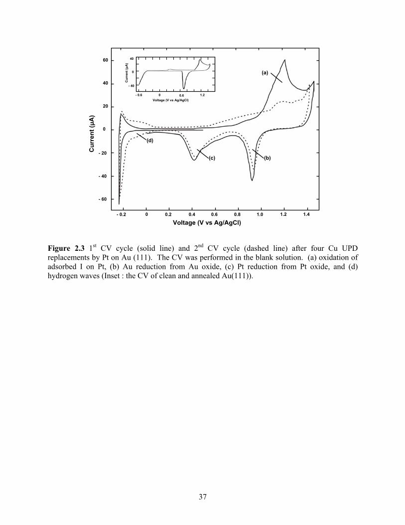
Figure 2.3 shows two CVs in the blank solution after four Pt replacement cycles with the
I atom layer present. The solid line is the first CV cycle, and the dashed line the second. The
CV was started negatively from 0.5 V, and the direction reversed at −0.3 V. It was then scanned
to 1.4 V, and reversed again, stopping at 0 V. The inset is the CV of clean and annealed Au(111).
At negative potentials, there is little evidence of the hydrogen waves, as expected, given the
presence of the I atom layer which blocks hydrogen adsorption. However, the reversibility of the
hydrogen reduction oxidation reactions is evident from the oxidation peak at −0.25 V indicating
the presences of Pt on the surface. The oxidation peak (a) results from the oxidation of adsorbed
I as indicated in Equation (2.2) [11]:
Iads + 3H2O → IO3− + 6H+ + 5e− (2.2)
In addition, peak (a) contains charge for the oxidation of both Pt and Au surface atoms. The
reduction peaks (b) and (c) were for reduction of Au and Pt surface oxides, respectively. Pt
coverage might be estimated from the relative sizes of the Pt and Au oxide reduction features, as
was done by Weaver et al [3]. However, electrochemical oxidation of Pt and Au is known to
disrupt nanoscale structure, possibly resulting in mixing of the surface atoms, place exchange.
Coulometric measurement of the Pt coverage by stripping is not an option, given that the surface
forms the passive oxide layer, rather than a soluble Pt species. In the second cycle, the dashed
31
curve, some charge for hydrogen adsorption is evident, the hydrogen waves, after the oxidative
removal of the adsorbed I atom layer. Quantification of hydrogen adsorption should also provide
a measure of the Pt surface atom coverage, as the hydrogen waves are generally felt to be the
adsorption of protons: one H atom for every Pt surface atom [3]. However, as the electrode was
first oxidized, the resulting surface structure and coverage are questionable. Future studies will
involve an initial reduction step to remove the adsorbed halide layer, prior to use of cyclic
voltammetry to study the hydrogen waves, and determine the Pt surface coverage.
Auger Electron Spectroscopy (AES)
Figure 2.4 shows AES spectra for (a) the clean Au(111), (b) after two cycles of Pt
replacement, and (c) four cycles of Pt replacement. The peak height of the principle Au Auger
peak (~ 69 eV) decreased as the replacement cycle increased, while the peak height of the
satellite Au Auger peak (~ 240 eV) remained almost the same regardless of the replacement
cycles. The lower energy Auger electrons are more easily scattered by the deposit, than the
higher energy electrons. The absence of a Cu Auger signal (~ 930 eV) in 2.4b and 2.4c and the
fact that the OCP during the Pt replacement shifted from 0.05 V to 0.75 V, suggested that Cu
was completely replaced by Pt. The doublet I Auger peak (~ 510 eV) shows that the deposits are
underneath the I adlayer, as the number of cycles performed does not effect its intensity. The
similarity of the Au Auger peak (~ 69 eV) and the Pt Auger peak (~ 67 eV) made it impossible to
differentiate the signals for Pt and Au, and thus to quantify the increasing Pt coverage.
Low-Energy Electron Diffractions (LEEDs)
Figure 2.5 shows LEED patterns: (a) for the clean Au(111), (b) the I modified Au, and
(c) after two Pt replacement cycle. The beam energies of (a), (b) and (c) LEED patterns were 52
eV, 48 eV and 52 eV, respectively. The LEED pattern corresponding to the clean and well-
32
ordered Au is a (1×1), prior to an electrochemical experiment. After adsorption of a I atom layer,
the sharp (√3×√3)R30°-I LEED pattern was evident (Figure 2.5b). (√7×√7)R19.1° or (3×3)
LEED patterns are expected for Pt in the presence of an I atom layer, according to the literature
[11]. However, a diffuse (√3×√3)R30°-I LEED pattern was observed after two Pt replacement
cycles, for a Pt coverage of 0.8 ML. The LEED pattern after four Pt replacements on Au showed
a diffuse (1×1), not shown. The diffused LEED patterns after the Pt replacement cycles on Au
may be the result of the formation of a surface Pt-Au alloy, which will be discussed in a
subsequent paper. Clearly, more LEED studies of these deposits are required.
STM studies, by this group, resulted in distinct images of the surfaces help in
understanding much of the result presented here, and will be published [12]. After one and two
Pt replacements on I modified Au(111), high resolution STM images suggested the presences of
disordered hexagonal shaped nano islands, and the five atom cluster and chains after various
numbers of cycles.
Conclusion
Surface limited redox replacement reactions (SLR3) of Pt for Cu UPD were studied using
UHV-EC methodologies. The possibility of Pt layer-by-layer growth was investigated. The Au
substrate was cleaned by Ar ion bombardment and annealed. The Au substrate was then
modified with an I atom layer, and Cu UPD was formed. This surface was then exposed to a
Pt(IV) solution at the open circuit, where the Cu UPD was exchanged for Pt over two minutes.
The OCP during the Pt replacement shifted from 0.05 V to 0.75 V.
CV in the blank solution after four Pt replacements on Au showed the oxidation of
adsorbed I, and the formation of Au and Pt oxides. On the subsequent negative going scan,
33
separate peaks for reduction of Au and Pt oxides were observed. After removal of the I atom
layer by oxidation, hydrogen waves were also observed. Estimation of the Pt coverage, from the
Pt reduction peak in the CV suggests that about 0.35 ML of Pt were deposited each cycle;
however, this was just a preliminary study, and 0.35 is a crude approximation. Studies to better
characterize these amounts are underway. The intensity of the I Auger peak suggested that I
remained on top of the deposited Pt. While the LEED pattern of the I modified Au showed a
(√3×√3)R30°-I, the LEED patterns after two and four Pt replacement cycles showed diffuse
(√3×√3)R30° and (1×1) patterns, respectively.
Acknowledgements
The support from Nation Science Foundation, Divisions of Materials and Chemistry, and
the Department of Energy is gratefully acknowledged.
References
1. K. Sieradzki, S. R. Brankovic, and N. Dimitrov, Science, 284, 138 (1999).
2. S. R. Brankovic, J. X. Wang, and R. R. Adzic, Surf. Sci., 474, L173 (2001).
3. M. F. Mrozek, Y. Xie, and M. J. Weaver, Anal. Chem., 73, 5953 (2001).
4. R. Vasilic and N. Dimitrov, Electrochem. Solid-State Lett., 8, C173 (2005).
5. M. P. Soriaga and J. L. Stickney, Modern Techniques in Electroanalytical Chemistry, p.
1~58, Wiley & Sons, New York (1996).
6. M. D. Lay and J. L. Stickney, J. Am. Chem. Soc., 125, 1352 (2003).
7. K. Varazo, M. D. Lay, T. A. Sorenson, and J. L. Stickney, J. Electroanal. Chem., 522, 104
(2002).
34
8. M. F. Toney, J. N. Howard, J. Richer, G. L. Borges, J. G. Gordon, O. R. Melroy, D. Yee,
and L. B. Sorensen, Phys. Rev. Lett., 75, 4472 (1995).
9. A. Martinez-Ruiz, J. Valenzuela-Benavides, L. Morales de la Garza, and N. Batina, Surf.
Sci., 476, 139 (2001).
10. A. Martinez-Ruiz, M. Palomar-Pardave, J. Valenzuela-Benavides, M. H. Farias, and N.
Batina, J. Phys. Chem. B, 107, 11660 (2003).
11. J. L. Stickney, S. D. Rosasco, and A. T. Hubbard, J. Electrochem. Soc., 131, 260 (1984).
12. Y. -G. Kim, J. Y. Kim, and J. L. Stickney, manuscript in preparation.
35
Figure 2.1 The Schematic diagram of UHV-EC system.
x-y-z Manipulator
Main Chamber
Cryopump
Ion Pump
Ante-Chamber
Electrochemical Cell
Sample Transporter
AES LEED
36
(a)
(b) (c)
Figure 2.2 (a) CVs of Cu on bare Au(111) (solid line) and Cu on I modified Au(111) (dashed line), (b) LEED pattern of 1st Cu UPD on I modified Au and (c) LEED pattern of Cu UPD at 0.05 V on I modified Au. Beam energies were 42 eV for (b) and 45 eV for (c).
- 40
- 20
0
20
40
Cur
rent
(µA
)
0 0.1 0.2 0.3 0.4Voltage (V vs Ag/AgCl)
37
Figure 2.3 1st CV cycle (solid line) and 2nd CV cycle (dashed line) after four Cu UPD replacements by Pt on Au (111). The CV was performed in the blank solution. (a) oxidation of adsorbed I on Pt, (b) Au reduction from Au oxide, (c) Pt reduction from Pt oxide, and (d) hydrogen waves (Inset : the CV of clean and annealed Au(111)).
Cur
rent
(µA
) 40
20
0
- 20
- 40
- 60
60
- 0.2 0 0.2 0.4 0.6 0.8 1.0 1.2 1.4
Voltage (V vs Ag/AgCl)
(d)
(a)
(c) (b)
Cur
rent
(µA
)
0
- 40
- 0.6 0 0.6 1.2Voltage (V vs Ag/AgCl)
40
38
0 100 200 300 400 500 600 700 800 900 1000
Electron Energy (eV)
dN(E
)/dE
(a)
(b)
(c)
Figure 2.4 Auger electron spectroscopies of (a) clean Au (111), (b) two cycles of Pt replacements, and (c) four cycles of Pt replacements.
39
(a)
(b)
(c)
Figure 2.5 LEED patterns of (a) clean Au (111) (beam energy: 52 eV), (b) I modified Au (111) (beam energy : 48 eV), and (c) two replacements Pt on Au (111) (beam energy : 52 eV).
40
CHAPTER 3
COPPER NANOFILM FORMATION BY ELECTROCHEMICAL ATOMIC LAYER
DEPOSITION (ALD) : UHV-EC AND IN-SITU STM STUDIES2
2 J.Y. Kim, Y.-G. Kim, and J.L. Stickney, J. Electrochem. Soc., 154, D260-D266 (2007).
Reprinted here with permission of publisher.
41
Abstract
Au(111) single crystal substrates were used in studies of Cu nanofilm formation by
electrochemical ALD. Cu UPD was used to deposit the first Cu atomic layer on a Au(111)
substrate, modified with an atomic layer of I atoms. By definition, Cu UPD results in the
formation of an atomic layer, thus, to deposit subsequent Cu, surface-limited redox replacement
(SLRR) was used. The SLRR involved initial formation of Pb UPD on the Cu coated surface
just described. This Pb UPD coated surface was then exposed to CuSO4 at OCP, where the Pb
atoms were exchanged for Cu. In the UHV-EC studies presented here, two Pb UPD potentials
were investigated: −0.400 V and −0.440 V. UHV-EC studies involved use of a surface analysis
instrument with optics for LEED and Auger, and to which was attached an ante-chamber
containing a Pyrex glass electrochemical H-cell. In this way, surface analysis was performed
without transfer of the deposit through air and the contamination which would result. In addition,
studies of the first few cycles of redox replacement were investigated using electrochemical in-
situ scanning tunneling microscopy (STM), with a flow cell for solution exchange to prevent loss
of potential control.
Introduction
In general, the electrochemical formation of metals occurs by nucleation and growth,
resulting in surface roughening [1], which increases as the deposit grows, similar to most vapor
deposition processes [2]. Development of 2D growth methodologies for nanofilm formation is
an important task, given that 2D growth modes should result in lower roughness, control of
deposit thickness, and increased crystallinity, as well as promoting epitaxy. The areas of atomic
layer epitaxy (ALE) and atomic layer deposition (ALD) are known to promote 2D growth, and
42
are based on the use of surface limited reactions. By application of surface-limited reactions in a
cycle, layer-by-layer growth of nanofilms results. The focus of this group has been the
application of ALD methodologies to the formation of semiconductor and metal nanofilms using
electrochemical versions of ALE or ALD [3].
Most electrochemical versions of ALD involve underpotential deposition (UPD), an
electrochemical surface-limited reaction. UPD is a phenomenon where an atomic layer of one
element deposits on a second at a potential prior to (under) that needed to deposit the element on
itself, the result of the thermodynamics of compound formation [3].
Historically, electrochemical forms of ALD have been applied in the formation of
compound semiconductors as UPD is defined for the formation of a single atomic layer of one
element on a second. In the case of compounds, UPD of the component elements might be
alternated to grow a deposit one atomic layer at a time; UPD of one element deposits on a second
and vice versa.
In order to electrodeposit pure metals layer-by-layer, in a 2D ALD mode, a novel
technique involving surface-limited redox replacement (SLRR) has been adopted. The method is
an outgrowth of work by Brankovic and Adzic [4], Weaver [5], Dimitrov [6], and Stickney [7].
Initial studies involved the desire to grow an atomic layer of a metal not readily formed via UPD,
such as Pt [4, 5]. The principle was that an atomic layer of a less noble metal could first be
deposited using UPD, and that surface would be exposed to a solution containing ions of a more
noble element, resulting in redox replacement of the less noble metal (sacrificial metal) for an
atomic layer of the more noble metal. Use of UPD limits deposition of the sacrificial element to
an atomic layer, which then serves to limit deposition of the more noble metal. The next step
was the realization that multiple cycles could be performed to create thicker films of these metals,
43
more than the atomic layer usually resulting from UPD [5]. Multiple cycles of Pt were
performed, but a number of questions resulted concerning quality and structure of the Pt films
formed. It was not clear that the deposits were growing strictly in a layer-by-layer format. It
appeared that some areas of the substrate may not have been covered, and the deposit
morphology appeared to quickly roughen in some cases. This is consistent with the history of Pt
electrodeposition, where the highly convoluted surface known as Pt black was generally formed.
Work by this group showed that the use of halides could improve the distribution of the
depositing Pt when combined with SLRR reactions, and that structures consistent with the
formation of a Pt surface were formed [7]. This use of an adsorbed halide has been referred to as
electrochemical annealing [8, 9].
The next step has been to show that this form of electrochemical ALD is a more general
method and can form other metals. In the initial studies of this process, single atomic layers of
Ag and Pd were both deposited [4]. Questions were then: can nanofilms be formed, with what
quality, how efficient is the exchange process, and can even less noble metals be deposited?
Which metals can be deposited to form nanofilms will depend on whether the sacrificial
metal can be underpotentially deposited on top of the more noble metal. It is in this way that
multiple atomic layers of a metal can be formed, repeating UPD of the sacrificial metal, and
exchange for the more noble metal in a cycle: electrochemical ALD. Adzic et al. replaced Cu
UPD with Pt(IV), Pd and Ag, and studied their deposits with scanning tunneling microscopy
(STM) [4]. Weaver et al. performed two, four, and eight replacement cycles using Cu UPD as
sacrificial layers, with Pt(II) and Pt(IV) and followed their results with cyclic voltammetry and
surface-enhanced Raman spectroscopy (SERS) [5]. Dimitrov et al. recently produced quasi-
44
perfect 2D growth of up to 35 layers of Ag on Au(111) using the SLRR reactions, using Pb UPD
as the sacrificial layers [6].
In this article, studies of the growth of Cu films, using Pb UPD as sacrificial layers, are
reported. Investigations were based on the use of ultrahigh vacuum (UHV) surface analytical
techniques directly with electrochemical experiments (UHV-EC) [10]. In addition, in-situ
scanning tunneling microscopy (STM) was used to follow the growth of the first few Cu layers
using a unique flow system [11]. Cu is more noble than Pb, and therefore should replace Pb
UPD spontaneously: Pb0UPD + Cu2+ → Pb2+ + Cu0. The resulting Cu atomic layers were studied
using Auger electron spectroscopy (AES) for surface composition and low-energy electron
diffraction (LEED) for surface order and the deposit unit cell. In-situ STM was used to follow
surface morphology and the structure of the I coated Cu deposits. The Pb replacement
efficiencies were determined using coulometry by following the amount of Pb deposited, and
then stripping the resulting Cu deposits.
In these studies, the surface of the substrate was coated with I atoms, in order to promote
electrochemical annealing. That is, an atomic layer of I atoms was formed spontaneously on the
Cu surfaces, yet did not significantly interfere with the exchange process. Adsorbed halides
were felt by the authors to provide extra mobility to the metal surface atoms, under certain
potential conditions. This was anticipated to allow deposited metal atoms to form a more perfect
adlayer, somewhat analogous to the effect of annealing, and thus the description as
“electrochemical annealing”. In addition, the adsorbed I atomic layers protected the Cu surface
from oxidation during emersion (withdrawal of the substrate from solution) and carbon
contamination which might have resulted. Finally, the structures of the halide layers on Cu are
45
well characterized [12], and relatively easy to image with STM, allowing monitoring of the
surface composition and structure.
Experimental
A disk-shaped Au(111) substrate, 1-cm in diameter and 1-mm thick, was used for the
UHV-EC studies. It was cleaned with hot concentrated HNO3, annealed in a hydrogen flame,
and then inserted into the UHV (~ 10−9 Torr) chamber. The Au(111) substrate was then cleaned
by Ar+ ion bombardment, and thermally annealed, in a cleaning procedures described elsewhere
[13]. It was then transferred to an ante-chamber, directly attached to the UHV system and
containing an electrochemical cell, where it was immersed for 2 min at open circuit in a 0.1 mM
solution of KI (J. T. Baker Chemical Co.), with 0.1 M HClO4 (Aldrich Co.), resulting in
adsorption of an atomic layer of I.
The KI solution was then exchanged for 1 mM CuSO4 (Aldrich Co.), with 5 mM H2SO4
(Aldrich Co.), and Cu UPD was formed at 0.050 V. All potentials are reported vs. Ag/AgCl (3
M KCl) (BioAnal). Pb UPD was then performed on the initial Cu UPD layer at −0.400 V or
−0.440 V, for 2 minutes. The Pb solution consisted of 0.5 mM Pb(ClO4)2 (Aldrich Co.), 0.25
mM KI, and 0.05 M HClO4 (Aldrich Co.). The resulting surfaces were then immersed in the Cu
solution for 10 seconds at open circuit, where the sacrificial Pb layer was exchanged Cu.
The above process, Pb UPD followed by exchange for Cu, was repeated between 1 and
10 times, followed by transfer to the UHV surface analysis chamber for analysis using AES
(Perkin-Elmer) and LEED (Princeton Research Instruments, Inc.). As a last step, the sample was
transferred back to the electrochemical cell in the ante-chamber, and the Cu was anodically
stripped to determine the Cu replacement efficiency (%). The efficiency was determined as a
46
function of the total charge for the initial Cu UPD, summed with the charges for each of the Pb
UPD steps in a particular experiment, and was thus a function of the number of cycles performed.
In-situ STM studies were performed using a Nanoscope III. The electrodes used were Au
single crystal beads made in house using the Clavilier methodology. Imaging was performed on
one of the resulting large (111) planes, clearly visible to the eye [7]. The electrochemical cell
was designed to allow solution to pass over the electrode, and through the cell. In this way,
solutions were exchanged without loss of potential control [11].
Results
Figure 3.1 displays CVs for Cu UPD on the clean Au(111) (solid line), and on an I-atom-
modified substrate (dashed line), both from the CuSO4 solution. In addition, a CV for Pb UPD
on an I-atom-modified Au(111) substrate, on which Cu UPD was present, is shown as the dot-
dashed curve at lower potentials in Figure 3.1. All three CVs were performed using the UHV-
EC instrument. The whole Au(111) slice was immersed in solution, so the voltammetry
represents the two main (111) faces, as well as the polycrystalline sides, and some
polycrystalline character is expected in the CVs. The scan rate was 5 mV/sec.
Comparing the solid and the dashed lines, in Figure 3.1, indicates that modification of the
Au(111) crystal with I atoms has shifted the first Cu UPD peak (clean Au(111)) negatively,
indicating that it is initially more difficult to deposit Cu on the I-coated surface [14]. On the
other hand, the second UPD peak for Cu on the clean substrate (solid line) is shifted positively
for deposition on the I-coated surface, so that in the case of the I-coated surface (dashed), both
peaks combined to form a large doublet for Cu UPD at 0.150 V. The net Cu UPD coverages for
depositions at 0.050 V were similar for both the clean and I-coated Au(111) substrate, very close
47
to a full monolayer (where a monolayer, ML, is defined as the deposition of one atom for every
surface Au atom). The CV for Cu UPD on the clean Au(111) surface is consistent with the
literature for Cu UPD from a sulfate solution [15, 16], while the dashed line for UPD on the I-
coated Au(111) is very similar to the work of Batina et al. [14], and reminiscent of Cu UPD on I-
coated Pt(111) [17].
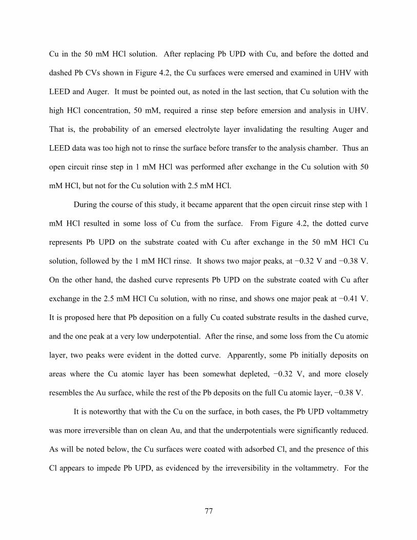
The CV for Pb UPD on clean Au(111) displays two features: at −0.200 V and −0.250 V
[18]. In Figure 3.1, the dot-dashed curve corresponds to deposition of Pb UPD on the surface
resulting from Cu UPD on the I atom-modified Au(111). This CV suggests that Pb UPD (dot
dashed) was shifted from −200 mV to −0.440 V (Figure 3.1), indicating a much lower Pb
underpotential, compared with clean Au(111). Under the conditions used (Figure 3.1) the charge
for Pb UPD formed at −0.440 V (~1 ML), on the initial Cu UPD, was nearly twice that for Pb
UPD formed at −0.400 V (~½ ML). Two sets of SLRR experiments were performed in this
study, both involving exchanging of a sacrificial Pb UPD layer for Cu. The first set involved Pb
UPD at −0.400 V, and the second set involved Pb UPD at −0.440 V. Given the nature of SLRR,
the more Pb UPD formed, the more Cu that should result.
Open circuit potentials (OCP) during exchange of Pb UPD for Cu were observed after
each replacement. The OCP for the first exchange, Pb UPD formed on the initial Cu UPD,
stabilized at 0.060 V. During subsequent exchanges, the OCP stabilized closer to 0.030 V. This
OCP (0.030 V) was consistent with the formal potential for the Cu2+/Cu couple: the presence of
bulk Cu. The high OCP for the first cycle (0.060 V) indicates the Cu deposit still resembled a
high coverage UPD rather than bulk Cu deposit, or that the surface was not completely covered,
and a mixed potential resulted.
48
Figure 3.2a displays the AES spectrum for Cu UPD at 0.050 V on I-modified Au(111),
where the ratio of the Cu (920 eV) to Au (240 eV) Auger peaks was about 1. The I doublet
(peaks at 511 and 518 eV) indicates the presence of an I atom layer on top. It is known that Cu
can be electrodeposited under an adsorbed I atom layer on some metals [17]. Given the
reactivity of Cu with oxygen, even the traces found in the UHP Ar used as the back fill gas in
these UHV-EC studies, an oxygen signal would have been expected if the Cu was not protected
by the I atom layer [19]. Figures 3.2b and 3.2c are AES spectra after Pb UPD at −0.400 V and
−0.440 V, respectively, on Cu UPD formed at 0.050 V, which was coated with I atoms. A Pb
peak is present at 95 eV, while the signals for both Au and Cu appear to decrease, their being
covered by Pb atomic layers. The Cu/Au ratio was greater than one, as expected, given that both
Pb and Cu were on top of the Au, and would scatter the Au Auger electrons. In addition, the
doublet for I at about 500 eV was gone, having been replaced by a peak for O (511 eV).
Although I-atoms adsorb strongly to Au and Cu, they do not strongly adsorb to Pb [18]. Thus,
Pb UPD can result in the loss of an I atom layer, so that the Pb surface oxidizes upon emersion
from solution, in the O2 traces found in the antechamber [20]. The Cl peak at 180 eV
corresponds to a very low coverage, also picked up in the antechamber upon emersion. The Cl
signal may, alternatively, indicate a small amount of emersed perchlorate electrolyte, which
would also account for some of the oxygen present, though not all of it.
Figure 3.3 shows AES spectra for (a) a clean Au(111), (b) after ten Cu replacement
cycles formed via Pb UPD at −0.400 V, and (c) after ten Cu replacement cycles formed via Pb
UPD at −0.440 V. The Auger ratio of the Cu peak (920 eV) to the Au peak (240 eV) in Figure
3.3b was Cu/Au = 6.4, significantly smaller than that in Figure 3.3c, Cu/Au = 17. This increase
in the Cu/Au ratio between 3.3b and 3.3c is consistent with each replacement of Pb UPD at
49
−0.400 V resulted in close to a ½ ML, while replacement of Pb UPD at −0.440 V was closer to 1
ML/cycle. The net result is that 10 cycles with Pb UPD at −0.400 V resulted in about 5 ML of
Cu deposited, while 10 cycles with Pb UPD at −0.440 V results in closer to 10 ML (Figure 3.4).
It is clear that the Cu/Au Auger ratios in Figures 3.3b (6.4) and 3.3c (17), are not 1:2, for
the deposits formed with Pb UPD potentials of −0.400 V and −0.440 V, respectively, as might be
expected. The use of Auger peak height ratios in this way is only linear for the first ML or so.
In the present study, although the coverages of Cu were increasing with each cycle, and thus the
Auger peak height for Cu, at the same time the Au peak height was decreasing, as Au Auger
electrons were increasingly scattered by the Cu over layer. Thus the relative ratio for deposits
formed at −0.400 V and −0.440 V was 6.4/17 (0.38) rather than the expected 0.5, based on
coverages. It is not clear that a Au signal should even be present after deposition of 10 ML of
Cu on the surface, given the limited mean free path of the Au electrons through the Cu film. The
presence of the Au signal may be an indication of the presence of some degree of surface
roughness.
Another difference between the Auger spectra in Figures 3.3b and 3.3c is that the
electrode surface in 3.3b was coated by I, the doublet near 500 eV, while the electrode in Figure
3.2c was coated by O, the singlet near 500 eV, suggesting an oxidized surface. Given that the
same procedures were used for each experiment, it is difficult to explain the presence of I atoms
in one case, and O in the other. The explanation probably involves the affinity of Pb for I atoms.
From previous studies of Pb UPD on I-coated Au, it is known that I does not bind strongly to Pb
under these conditions [18]. However, at lower Pb UPD coverages on Au, Pb and I can coexist
adsorbed on the surface. Given the affinity of Au and Cu for I atoms, Pb and I on Cu probably
behave similarly. In the present study the Pb solution contained KI, so that after Pb UPD at
50
−0.400 V, some I atoms may have remained adsorbed on the surface during transfer to the Cu
solution. Upon redox replacement of the Pb with Cu, I atoms would strongly adsorb on the Cu
surface. In the case where Pb UPD was performed at −0.440 V, no I atoms would have remained
adsorbed due to the high Pb coverage, and thus no I atoms were transferred with the deposit and
immersed in the Cu2+ solution. The resulting Cu surface was thus unprotected by I atoms upon
emersion from the Cu solution and transfer to the analysis chamber. As noted above,
unprotected Cu oxidizes upon emersion and transfer (Figure 3.3c).
Figure 3.4 shows stripping charges for all deposited Cu, as a function of the number of
cycles performed and the Pb UPD potential used. The squares are for Pb UPD at −0.440 V,
while the diamonds are for Pb UPD at −0.400 V. Charges are reported as ML, relative to the Au
surface. The linear changes in coverage with the number of cycles are characteristic of an ALD
process.
Figure 3.5a displays LEED patterns for the clean substrate, a Au(111)(1×1), while Figure
3.5b is the pattern for an I-modified Au(111) surface, a Au(111)(√3×√3)R30º-I, corresponding to
1/3 ML coverage of I [21]. In Figure 3.5c and 3.5d are the observed LEED patterns for Cu UPD
on I-coated Au at 0.050 V and Cu UPD with the addition of one Cu replacement, using Pb UPD
at −0.400 V, respectively. Both images showed diffuse and somewhat distorted (3×3) patterns.
No pattern was evident, just diffuse intensity, for the surface resulting from Cu replacement of
Pb UPD deposited at −0.440 V. This was expected given that the Auger spectrum in Figure 3.3c
showed an oxidized surface, which generally result in a disordered surface. However, if a
similar surface (Cu UPD and one redox replacement of Pb UPD with Cu at −0.440 V) was then
immersed in the KI solution, at open circuit, the diffused (3×3)-I LEED pattern shown in Figure
51
3.6a was observed. After five replacements of Pb UPD (at −0.440 V), and immersion into the KI
solution, a diffuse (√3×√3)R30°-I pattern was observed (Figure 3.6b).
Images from in-situ STM studies, by this group, are displayed in Figure 3.7. The first
image is of a (3×3)-I structure formed on the Au(111) surface, modified with an atomic layer of I
atoms, during Cu UPD. Similar images were observed at potentials corresponding to the UPD
doublet, shown in Figure 3.1 (dashed). Figure 3.7b is the image of a large scan, showing large
terraces after Cu UPD on the I-coated Au surface. Figures 3.7c and 3.7d are larger area images
of the surface after UPD and one redox replacement. Figure 3.7c was first, followed three
minutes latter with 3.7d. It is evident from these images that the more cycles performed, the
more monoatomic pits and islands present on the surface. However, the annealing process was
relatively fast, showing that the atoms were mobile: the islands disappeared and pits filled in. In
addition, there was growth at step edges, in some cases taking the form of single atom high
fingers protruding out from the step edge, Figures 3.7c and 3.7d. Figure 3.7e shows the surface
after Cu UPD and two cycles of Pb UPD replacement by Cu which displays more pits and
islands. Again this morphology anneals with time. After Cu UPD and three replacements, the
images in Figures 3.7f and 3.7g were obtained. Note that some of the pits were two monolayers
deep. Figures 3.7g is a close up, showing the presence of a well ordered (√3×√3)R30°-I lattice
on the Cu surface, as well as a look in the pits that may penetrate to the first Cu UPD layer on Au.
Figure 3.8 shows the replacement efficiency (RE), versus the number of Cu replacement
cycles for Pb UPD at −0.400 V and at −0.440 V. The efficiencies were calculated as %: [[(total
Cu Q) − (initial Cu UPD Q)] / (Σ Pb UPD Qs)] × 100 = % RE. Total Cu charge was calculated
from anodic stripping voltammetry after deposit formation. The initial Cu UPD charge and Pb
UPD charges were the integrated deposition currents. Efficiencies for deposits formed using Pb
52
UPD at −0.400 V are displayed as diamonds, while those for deposits formed using Pb UPD at
−0.440 V are displayed as squares. For deposits formed with Pb UPD at −0.400 V, the
efficiency decreased from near 100% to 60% as the number of Cu redox replacement cycles
increased. On the other hand, the efficiencies for Cu redox replacement of Pb UPD at −0.440 V
showed significant variability, but averaged about 84%.
Discussion
In general, the unit cells of deposits formed in this study were in agreement with those
observed for Cu UPD on I-coated Au(111) or I-coated Cu(111), found in the literature [12, 14,
22]. That is, in detailed studies of the UPD of Cu on I-coated Au(111), Batina et al. observed a
(3×3)-I unit cell [14], and a (√3×√3)R30º-I structure was observed for I atoms adsorbed on bulk
Cu(111) [12]. However, Batina et al., using in-situ STM, only observed the (3×3)-I structure for
very low coverages of Cu. They concluded that the Cu coverages were so low as to not account
for the (3×3), but that the Cu merely served to stress the I atom layer, and converted it to the
(3×3)-I structure. This does not appear to account for all the (3×3) LEED patterns observed in
the present study (Figures 3.5 and 3.6) or coincide with all the in-situ STM results obtained by
this group.
Possible explanations for these discrepancies include: some domains in the present
studies involved low coverages of Cu, while others may have had multiple Cu layers. In other
words, there was a mixture of domains on the surface. It is believed that between ½ and 2 ML of
Cu were present on the surface when the (3×3)-I LEED patterns were observed (Figures 3.5c and
3.5d, as well as Figure 3.6), depending on the number of ALD cycles, and the potential used for
Pb UPD. It is evident from the STM images (Figure 3.7) that the surface was not
53
homogeneously covered after a given number of cycles, but displayed both islands and pits. In
addition, given the OCP observed for these deposits, at least a ½ ML of Cu UPD would
thermodynamically be required in any domains on the surface not covered with multiple Cu
layers, the pit bottoms for example.
It is also possible that some Cu was lost during the emersion and re-immersion steps
between solutions. This may account for exchange efficiencies less than 100 %, and possibly the
presence of areas on the surface with lower Cu coverages, where the (3×3)-I LEED patterns
originated. The emersion and evacuation process could change the surface structure observed,
but halide coated metal surfaces, such as I on Pt, Au and Cu, are well known to show similar
structures in UHV and via in-situ STM. No emersion etc. was used in the in-situ STM studies,
were the (3×3)-I structures were observed, and where the potentials prevented loss of UPD Cu
from the surface. Although, in this study, STM images of the (3×3)-I structure was not observed
for Cu coverages in excess of about 0.6 ML, as in the work of Batina et al. [14]. It is noteworthy
that in other Cu nanofilm growth studies by this group, using a flow deposition system so no
emersions and immersions were involved, efficiencies very close to 100% were observed in
some cases.
Conclusions drawn by the Authors were that even with Cu UPD coverages above ½ ML
on the surface of I-coated Au(111), domains with a (3×3)-I unit cell did exist. During UHV-EC
studies of Cu ALD, where the deposit was emersed and immersed, some Cu may have been lost.
However, from Auger studies, as well as the efficiency studies, only a small % of the Cu was lost,
possibly from isolated domains, dropping the Cu coverage, and thus accounting for the (3×3)-I
LEED patterns observed even when the overall coverage was higher. To avoid such issues in
54
future studies, a flow cell is being constructed so that solutions can be exchanged in the UHV-
EC studies without emersion, or loss of potential control, until transfer to UHV for analysis.
It is encouraging that the LEED patterns seen at higher coverages of Cu did display the
expected (√3×√3)R30º-I, previously observed on Cu(111) [12, 22], via in-situ STM. It would
have been good to be able to determine at what coverage the structure converts from (3×3) to
(√3×√3)R30º-I, but results from this group and the literature suggest that there is some ill defined
structure which grows in after the (3×3)-I in Cu UPD studies on I-coated Au(111) [14]. The
(√3×√3)R30º-I, on the other hand, does appear at coverages between 2 and 3 ML, in both STM
and UHV-EC studies.
Conclusions
Surface-limited redox replacement of Pb UPD to form atomic layers of Cu has been
studied. Pb UPD as sacrificial layers, to deposit Cu atomic layers, has been used in an ALD
cycle to grow smooth nanofilms of Cu. UHV-EC and in-situ STM were used to follow the
composition, structure and morphology of Cu film growth. The extent of film growth at the
monolayer level was controlled by the number of cycles performed and the Pb UPD potential.
However, deposit surface morphology was rougher than anticipated. Given sufficient time, the
atomic layers do anneal out, and it is anticipated that by optimizing times, potentials and halide
introduction, deposit morphology will improve. It is important to keep in mind that the
morphology which would result from standard electrodeposition methodologies at room
temperature would likely result in nucleation growth and the associated morphology. With such
as a comparison, these films had excellent morphology.
55
The surface structures observed were consistent with the literature, except that the (3×3)-I
structure observed for Cu deposition on I-coated Au(111) appeared at higher Cu coverages than
expected from the literature. There are a number of plausible explanations, including that
domains supporting different structures were present simultaneously on the surface, or that
during UHV-EC studies some Cu may have been lost from the surface, resulting in lower
replacement efficiencies and possibly accounting for the domain variability suggested. Use of a
flow through cell during UHV-EC studies should provide more consistency, as well as higher
exchange efficiencies.
Acknowledgements
The financial support from National Science Foundation, Divisions of Materials and
Chemistry and the Department of Energy, is gratefully acknowledged.
References
1. M. Fleischmann and H.R. Thirsk, in Advances in electrochemistry and electrochemical
engineering, P. Delahay and C.W. Tobias (Eds.), Interscience Publishers, John Wiley and
Sons, Inc., New York, 1963.
2. H.O. Pierson, Handbook of chemical vapor deposition, Noyes Publications, Park Ridge,
NJ, 1992.
3. J.L. Stickney, in Advances in Electrochemical Science and Engineering, R.C. Alkire and
D.M. Kolb (Eds.), Wiley-VCH, Weinheim, 2002.
4. S.R. Brankovic, J.X. Wang, and R.R. Adzic, Surf. Sci., 474, L173 (2001).
5. M.F. Mrozek, Y. Xie, and M.J. Weaver, Anal. Chem., 73, 5953 (2001).
56
6. R. Vasilic and N. Dimitrov, Electrochem. Solid-State Lett., 8, C173 (2005).
7. Y.-G. Kim, J.Y. Kim, D. Vairavapandian, and J.L. Stickney, J. Phys. Chem. B, 110,
17998 (2006).
8. I. Villegas, C.B. Ehlers, and J.L. Stickney, J. Electrochem. Soc., 137, 3143 (1990).
9. J.L. Stickney, I. Villegas, and C.B. Ehlers, J. Am. Chem. Soc., 111, 6473 (1989).
10. M.P. Soriaga and J.L. Stickney, Chemical Analysis (New York), 139, 1 (1996).
11. M.D. Lay, T.A. Sorenson, and J.L. Stickney, J. Phys. Chem. B, 107, 10598 (2003).
12. J. Inukai, Y. Osawa, and K. Itaya, J. Phys. Chem. B, 102, 10034 (1998).
13. J.Y. Kim, Y.-G. Kim, and J.L. Stickney, Electrochem. Soc. Trans., 1, 41 (2006).
14. A. Martinez-Ruiz, J. Valenzuela-Benavides, L.M. de la Garza, and N. Batina, Surf. Sci.,
476, 139 (2001).
15. M.F. Toney, J.N. Howard, J. Richer, G.L. Borges, J.G. Gordon, and O.R. Melroy, Phys.
Rev. Lett., 75, 4472 (1995).
16. M. Dietterle, T. Will, and D.M. Kolb, Surf. Sci., 342, 29 (1995).
17. J.L. Stickney, S.D. Rosasco, B.C. Schardt, and A.T. Hubbard, J. Phys. Chem., 88, 251
(1984).
18. Y.-G. Kim, J.Y. Kim, C. Thambidurai, and J.L. Stickney, in preparation, (2006).
19. C.B. Ehlers and J.L. Stickney, Surf. Sci., 239, 85 (1990).
20. B.C. Schardt, J.L. Stickney, D.A. Stern, A. Wieckowski, D.C. Zapien, and A.T. Hubbard,
Surf. Sci., 175, 520 (1986).
21. J.E. Harris, M.E. Bothwell, J.F. Rodriguez, M.P. Soriaga, and J.L. Stickney, J. Phys.
Chem., 93, 2610 (1989).
22. R. Randler, M. Dietterle, and D.M. Kolb, Z. Phys. Chem., 208, 43 (1999).
57
Figure 3.1 Cyclic voltammetries of Cu on bare Au(111) (solid line), Cu on I-modified Au(111) (dashed line), and Pb on Cu UPD (dot-dashed line). Scan rate = 5 mV/sec. Inset: Pb CV on bare Au(111).
Voltage (V vs. Ag/AgCl)
- 40
- 20
0
20
40 C
urre
nt (µ
A)
0 0.1 0.2 0.3 0.4- 0.1- 0.2- 0.3 - 0.4 - 0.5
- 60
58
0 100 200 300 400 500 600 700 800 900 1000
Electron Energy (eV)
dN(E
)/dE
(a)
(b)
(c)
Figure 3.2 AES spectra of (a) the initial Cu UPD at 0.050 V on I-modified Au(111), (b) after Pb UPD at −0.400 V on the initial Cu UPD, and (c) after Pb UPD at −0.440 V on the initial Cu UPD.
59
0 100 200 300 400 500 600 700 800 900 1000
Electron Energy (eV)
dN(E
)/dE
(a)
(b)
(c)
Figure 3.3 AES spectra of (a) clean Au(111), (b) after ten Cu replacements with Pb UPD at −0.400 V, and (c) after ten Cu replacements with Pb UPD at −0.440 V.
60
1
2
3
4
5
6
7
8
9
10
11
0 1 2 3 4 5 6 7 8 9 10 11
Number of Replacement Cycles
Repl
aced
Cu
Char
ge (M
L vs
Au)
Figure 3.4 Replaced Cu anodic stripping charge (ML vs Au) versus the number of replacement cycles; Squares: Cu replacements with Pb UPD at −0.440 V; Diamonds: Cu Replacements with Pb UPD at −0.400 V; Solid lines: the best-fit lines.
62
(c)
(d)
Figure 3.5 LEED patterns of (a) clean Au(111) (beam energy = 45.0 eV), (b) I-modified Au(111) (beam energy = 48.0 eV), (c) Cu UPD at 0.050 V on I-modified Au(111) (beam energy = 45.0 eV), and (d) after one Cu replacement with Pb UPD at −0.400 V (beam energy = 45.0 eV).
63
(a)
(b)
Figure 3.6 LEED patterns of (a) I modification of one Cu replacement with Pb UPD at −0.440 V (beam energy = 43.0 eV) and (b) I modification of five Cu replacements with Pb UPD at −0.440 V (beam energy = 45.0 eV).
67
(g)
Figure 3.7 In-situ STM images of (a) after Cu UPD on I-modified Au(111) (20 × 20 nm2), (b) after Cu UPD on I-modified Au(111) (300 × 300 nm2), (c) after Cu UPD and one Cu replacement (300 × 300 nm2), (d) three minutes after (c) (300 × 300 nm2), (e) after Cu UPD and two Cu replacements (300 × 300 nm2), (f) after Cu UPD and three Cu replacements (200 × 200 nm2), and (g) after Cu UPD and three Cu replacements (20 × 20 nm2).
68
50
60
70
80
90
100
110
0 1 2 3 4 5 6 7 8 9 10 11
Number of Replacement Cycles
Effic
ienc
y (%
)
Figure 3.8 Replacement efficiency (%) versus the number of replacement cycles; Square: Cu replacements with Pb UPD at −0.440 V; Diamond: Cu replacements with Pb UPD at −0.400 V.
69
CHAPTER 4
CU NANOFILM FORMATION BY ELECTROCHEMICAL ATOMIC LAYER DEPOSITION
(ALD) IN THE PRESENCE OF CHLORIDE IONS3
3 J.Y. Kim, Y.-G. Kim, and J.L. Stickney, Accepted by J. Electroanal. Chem. (2007).
Reprinted here with permission of publisher.
70
Abstract
The effect of Cl− on the structure of Cu nanofilms deposited with electrochemical ALD, using
surface limited redox replacement (SLRR), is described. These investigations involved ultrahigh
vacuum analytical methodologies coupled directly with electrochemical studies (UHV-EC), as
well as in-situ scanning tunneling microscopic (STM) studies. Pb was chosen as the sacrificial
metal as it forms atomic layers on Cu via underpotential deposition (UPD). In addition, it is
significantly more reactive than Cu, less noble, and thus undergoes redox replacement by Cu. Pb
UPD was formed at −0.44 V versus Ag/AgCl, for 20 seconds. The substrates used in these
studies were Ar+ ion bombarded and annealed Au(111) single crystal substrates. The resulting
Pb UPD coated Au(111) was immersed in a Cu2+ ion solution at open circuit for 10 seconds,
allowing redox replacement of the Pb UPD by Cu. Nanofilms were then formed by repeating
this process of Pb UPD followed by exchange for Cu. The resulting Cu nanofilms were
characterized using low-energy electron diffraction (LEED), Auger electron spectroscopy (AES),
and in-situ STM. The total Cu in a deposit was estimated by anodic stripping. Up to five cycles
of Pb replacement by Cu were performed in these studies. The structures formed displayed a (5
× 5) unit cell, consisting of a 4 by 4 arrangement of Cl atoms on the Cu surface. The degree of
surface order appeared to decrease gradually as the number of replacement cycles was increased,
though a relatively clear LEED pattern was still observed after 5 replacement cycles.
Keywords: Electrochemical ALD; Surface-Limited Redox Replacement (SLRR); UHV; UPD;
LEED; EC-STM; Electrochemical Annealing (EA)
71
Introduction
Besides halide anions (F−, Cl−, Br−, and I−) being common components of supporting
electrolytes, they are known to act as surfactants on metal surfaces, and have been used in what
is referred to here as electrochemical annealing (EA) [1, 2]. EA describes a process where the
surface of a metal is smoothed at the atomic scale by a combination of the adsorption of a
surfactant species and adjustment of the electrochemical potential to near that required to oxidize
the metal [3, 4]. This combination appears to promote surface mobility, and thus ordering. Most
EA studies have involved adsorbed halides as surfactants on some of the more noble metal
substrate surfaces, such as Au [1], Cu [5] and Pd [6], although CO has also been suggested as a
surfactant which promotes EA [7]. The idea is that by complexing the surface atoms with an
adsorbate, and using relatively positive potentials, allowing extra surface mobility, and thus
surface smoothing. This appears to result from a weakening of the metallic bonding between the
first and second metal layers [8]. Adsorbed halides are also known to protect Pt surfaces from
contamination, as they are well known to form ordered atomic layers epitaxially on metal
substrate surfaces [9]. I− is especially well known for this, as these anions spontaneously adsorb
as layers of neutral I atoms, oxidative adsorption, even at open circuit [1]. In addition, in
ultrahigh vacuum electrochemical studies (UHV-EC), adsorbed halide layers have been known
to prevent surface reconstructions [10], or upon adsorption, to lift reconstructions.
Underpotential deposition (UPD) is a phenomenon where an atomic layer of a less noble
element is deposited on a second, more noble, element. Deposition stops after formation of an
atomic layer, as the surface area is limited, and the depositing element no longer has access to
the substrate element. It is the result of the free energy of formation of a surface compound or
alloy [11]. There are numerous studies of metal UPD on surfaces supporting adsorbed halide
72
layers [9, 12-15]. Such atomic layer formation occurs at a potential prior to (under) that needed
to deposit the element on itself (bulk deposition) and thus is referred to as UPD. Behm et al. and
Kolb et al. presented in-situ scanning tunneling microscopy (STM) images to demonstrate the
influence of a trace of Cl− (10−4 M) on the UPD of Cu on Au(100) [16] and Au(111) [17]. They
suggested that coadsorbed Cl− anions stabilize the Cu adlayer, resulting in a sharp adsorption
peak in the I−V curve at 0.295 V, versus a saturated calomel electrode (SCE), and that the anions
effectively lead to strongly attractive interactions between the Cu adatoms, indicated by the
observation of (n × 2) islands, in a trace of Cl−. Matsumoto et al. also used traces of Cl−, Br−, or
I−, in Cu solutions (50 mM H2SO4 + 1 mM CuSO4) to investigate the coadsorption of Cu and
halide anions on Pt(111), Pt(100), and Au(111) [15]. Their STM images of coadsorbed Cu and
halide structures on Au(111) revealed a (5 × 5) structures for Cu + Cl, after the first cathodic
UPD peak (0.450 V vs. SHE), as well as after the second (0.310 V). Structures formed by the
deposition of Cu in the presence of Br− displayed (√7 × √7)R19.1° and (4 × 4) structures after the
first (0.450 V) and second (0.375 V) UPD deposition peaks, respectively, and a (3 × 3) structure
for Cu deposition in the presences of I− (0.380 V). Lipkowski et al. proposed models surface
structures for Cl− coadsorbed with Cu UPD, from studies combining electrochemical
methodologies and polarization-resolved X-ray absorption spectra (XAS) [18]. The
electrodeposited copper atoms were packed between the outer Au surface layer and under the
chloride capping layer, resulting in a (5 × 5) surface unit cell.
The present report involved UHV-EC [19] and in-situ STM studies of the formation of
Cu nanofilms formed using electrochemical ALD, in the presence of Cl−. ALD stands for atomic
layer deposition, a thin film formation methodology based on the layer-by-layer growth of thin
films using surface limited reactions. UPD is a prominent example of an electrochemical surface
73
limited reaction; however, it results only in the formation of a single atomic layer. To form more
than one atomic layer, a cycle is needed, with each resulting in the formation of an atomic layer.
Repeating the cycle linearly increases the deposit thickness. As noted, there must be more to the
cycle than UPD, as by itself, UPD only results in formation of a single atomic layer. To form
metal nanofilms, cycles have been developed using surface limited redox replacement (SLRR)
[20]. The principle developed by Brankovic and Adzic was that if the metal you desire to
deposit does not form an atomic layer, take a more reactive metal (the sacrificial metal) that will
form an atomic layer by UPD and exchange it in a solution of an ionic precursor for the metal
you want. The amount exchanged will be limited by the electrons available in the sacrificial
atomic layer, as when it has been dissolved, no more deposition will take place.
This process was first used in a cycle by the late Mike Weaver [21] to grow Pt nanofilms.
Electrochemical ALD nanofilms of Pt have also been reported by Kim et al. [1]. Formation of
Cu nanofilms using electrochemical ALD has been recently reported by both the authors [2] and
Dimitrov et al. [22].
Experimental
A 1.0 cm diameter Au(111) single crystal disk, 1-mm thick, was used as the substrate for
the UHV-EC studies. It was cleaned in vacuum using Ar+ ion bombardment (IBB), 1 µA/cm2,
and annealing by resistance heating. Figure 4.1a shows the (1 × 1) LEED pattern, 50 eV, of the
clean Au(111) surface after IBB and annealing. The clean substrate was transferred to the ante-
chamber, without exposing to air. The ante-chamber was then back-filled with ultrahigh purity
(UHP) Ar gas and the electrochemical cell was inserted. Solutions were pumped into the cell
using pressurized Pyrex bottles. All potentials noted in this article are reported with respect to a
74
Ag/AgCl (3M KCl) reference electrode. The solutions used were de-aerated with UHP Ar gas
for about 30 minutes prior to each electrochemical experiment.
The Pb2+ ion solution, 0.25 mM Pb(ClO4)2 (Aldrich Co.) + 50 mM HCl (Aldrich Co.),
was introduced into the electrochemical cell, before the Au(111) crystal lowered in, and
underpotential deposition was performed at −0.44 V for 20 seconds. The resulting sacrificial
metal Pb UPD layer was then immersed into the Cu2+ solution, where it was replaced at open
circuit for 10 seconds:
PbUPD + Cu2+ → Pb2+ + Cubulk (4.1)
This process was repeated to grow thicker films. After the desired number of Cu replacement
cycles, the electrochemical cell was removed, the ante-chamber pumped down, and the substrate
transferred back to the main chamber for characterization with LEED (Princeton Research
Instrument, Inc.) and Auger Electron Spectroscopy (AES) (Perkin-Elmer). Finally, the sample
was transferred back to the ante-chamber for anodic stripping of the deposited Cu in the blank, 1
mM HCl, to estimate the total Cu coverage in monolayers (ML). A ML was defined in the
present study as one atom for every Au surface atom (1.35 × 10¹⁵ atoms/cm2 for a smooth (111)
surface). After the anodic stripping of Cu, the replacement efficiency was determined as
follows:
Cu Replacement Efficiency = (Charge for stripping Cu)/Σ(Pb UPD charges) (4.2)
Both processes involved two electrons, so ideally one Cu atom should result from each Pb atom
deposited. The total Cu charge was determined by anodic stripping voltammetry, while Pb UPD
charges were determined from the current-time traces for deposition.
In the UHV-EC studies, Cu2+ solutions of two HCl concentrations were investigated: 1
mM Cu(ClO4)2 (Aldrich Co.) + 50 mM HCl; and 1 mM Cu(ClO4)2 + 2.5 mM HCl. In UHV-EC
75
studies it is well known that aqueous solutions with electrolyte concentrations of 10 mM or
above are generally problematic, as the emersion layer (that layer of solution dragged with the
crystal when it is removed from solution) contains sufficient salts which, upon evaporation,
crystallize on the surface, degrading LEED patterns, and raising questions concerning the nature
of Auger peaks present in the spectrum. One way around this problem is to rinse the sample
with a dilute solution, after emersion (removal) of the substrate from a solution, to decrease the
electrolyte concentration in the emersion layer. This can be performed at open circuit, or
controlled potential. In the present case, deposits formed using the 50 mM HCl solution were
rinsed with 1 mM HCl blank solution prior to transfer to the analysis chamber, while those from
the 2.5 mM HCl solution were simply emersed and transferred, without the rinse. After
characterization with LEED and AES, the deposits were transferred back to the ante-chamber for
coulometric stripping of the deposited Cu.
In-situ STM studies, performed using a Nanoscope III (Digital Instruments, Santa
Barbara, CA), were used to confirm the surface structures in-situ. For the STM studies, Au
single crystal beads were formed using the method developed by Clavilier [23], and imaging was
performed on one of the resulting large (111) planes of the single crystal bead. The
electrochemical cell was designed to allow solution to pass over the electrode so that the
solutions could be exchanged without loss of potential control during imaging [24].
Results and Discussion
The solid line, Figure 4.2, corresponds to the voltammetry for Pb2+ UPD on bare Au(111)
from the Pb solution described above. Note, although the front and back of the crystal were
polished to [111] orientations, the sides were still polycrystalline. Since the whole crystal was
76
immersed in solution, to perform electrochemical experiments, the voltammetry displayed in this
article retains some polycrystalline features. The scan rate used for Figure 4.2 was 5 mV/sec. Of
note in this voltammetry is the relative reversibility of Pb UPD on the clean surface (solid line).
The first Pb UPD features were observed at about −0.1 V, a low broad hump with a few sharp
spikes. The second grouping of UPD peaks began closer to −0.2 V, and consisted of at least
three large sharp peaks. In total, the Pb UPD charge after scanning to −0.44 V was equivalent to
the deposition of about 0.95 ML, consistent with the literatures [25-27]. These large UPD
features suggest the majority of the Pb experiences an underpotential of about 200 mV. AES
spectra obtained after Pb UPD below −0.3 V indicated the presence of Pb (90 eV), with a Pb/Au
(240 eV) Auger peak ratio of about 4, and the presence of small amounts of O (510 eV) and Cl
(180eV). It has been shown in studies of Pb UPD on Pt that some Pb tends to oxidize upon
emersion from various lead halide solutions [28-30] during the transfer process in UHV-EC
studies, probably accounting for the small oxygen Auger signal. The studies of Pb deposition
from Cl and Br solutions on Pt surfaces suggested that at lower coverages of Pb, less than 0.5
ML, halides were co-adsorbed with Pb [28, 30]. The Cl signal may thus be from Cl atoms
adsorbed in areas where some Pb was lost during the transfer, where the Pb coverage was lower.
Previous studies with I− adsorption on Pb UPD on Au(111) indicated that I co-adsorbed with Pb
only up to a coverage of 0.44 ML, and desorbed in the presences of higher Pb coverages [31],
suggesting other halides, Cl for instance, may desorb in the presences of high Pb coverages. The
Cl signal was not very significant, corresponding to much less than 5 % of a monolayer.
The dotted and dashed lines in Figure 4.2 are Pb CVs for surfaces after one cycle of Cu
deposition. The dashed curve was the surface resulting from exchange of Pb for Cu in the 2.5
mM HCl solution, while the dotted curve was for the surface resulting from exchange of Pb for
77
Cu in the 50 mM HCl solution. After replacing Pb UPD with Cu, and before the dotted and
dashed Pb CVs shown in Figure 4.2, the Cu surfaces were emersed and examined in UHV with
LEED and Auger. It must be pointed out, as noted in the last section, that Cu solution with the
high HCl concentration, 50 mM, required a rinse step before emersion and analysis in UHV.
That is, the probability of an emersed electrolyte layer invalidating the resulting Auger and
LEED data was too high not to rinse the surface before transfer to the analysis chamber. Thus an
open circuit rinse step in 1 mM HCl was performed after exchange in the Cu solution with 50
mM HCl, but not for the Cu solution with 2.5 mM HCl.
During the course of this study, it became apparent that the open circuit rinse step with 1
mM HCl resulted in some loss of Cu from the surface. From Figure 4.2, the dotted curve
represents Pb UPD on the substrate coated with Cu after exchange in the 50 mM HCl Cu
solution, followed by the 1 mM HCl rinse. It shows two major peaks, at −0.32 V and −0.38 V.
On the other hand, the dashed curve represents Pb UPD on the substrate coated with Cu after
exchange in the 2.5 mM HCl Cu solution, with no rinse, and shows one major peak at −0.41 V.
It is proposed here that Pb deposition on a fully Cu coated substrate results in the dashed curve,
and the one peak at a very low underpotential. After the rinse, and some loss from the Cu atomic
layer, two peaks were evident in the dotted curve. Apparently, some Pb initially deposits on
areas where the Cu atomic layer has been somewhat depleted, −0.32 V, and more closely
resembles the Au surface, while the rest of the Pb deposits on the full Cu atomic layer, −0.38 V.
It is noteworthy that with the Cu on the surface, in both cases, the Pb UPD voltammetry
was more irreversible than on clean Au, and that the underpotentials were significantly reduced.
As will be noted below, the Cu surfaces were coated with adsorbed Cl, and the presence of this
Cl appears to impede Pb UPD, as evidenced by the irreversibility in the voltammetry. For the
78
surface with a slightly higher Cu coverage, the dashed curve, the UPD features are closer to bulk
deposition, as the surface has a more complete coating of Cl.
Figure 4.1b shows the LEED pattern after Pb UPD at −0.44 V on the bare Au(111)
surface. The pattern consists of a ring of twelve spots, with another ring of twelve inside, rotated
by 15 degrees, one third of the way in from the integral beams. Some disorder in the structure is
indicated by the diffuse intensity of the pattern. The rings suggest that the structure has multiple
domains, rotated from each other on the surface. Previous studies in the deposition of Pb on
Au(111) indicated a Moiré pattern structure [31]. The uniqueness of the LEED pattern does not
appear inconsistent with the presence of a Moiré structure, however, at present the unit cell and
relationship of the pattern with respect to the Moiré is not clear.
Figure 4.3a shows Cu UPD CVs on bare Au(111) using the 50 mM HCl Cu solution
(solid line) and the 2.5 mM HCl Cu solution (dotted line), both at 5 mV/sec. Similar CVs have
been published by other workers [12, 32]. The main Cu UPD peak, in the 50 mM HCl solution,
occurred at about 0.325 V, and showed strong reversibility, while that for the 2.5 mM HCl
solution was at 0.3 V, and showed significant splitting in the peaks, some irreversibility. It is
interesting that for the higher HCl concentration, the deposition peak was sharper and more
reversible, suggesting the deposition mechanism fundamentally involved chloride. The dashed
curve in Figure 4.3a was for Cu UPD in a “chloride free” solution (1 mM Cu(ClO4)2 + 50 mM
HClO4), where no sharp deposition feature was evident, although there were two prominent
peaks in the oxidation scan at 0.15 V. It should be noted, that previous studies with Cu surfaces
have clearly shown that “chloride free” electrolyte is hard to come by, given the tenacity of Cl−
adsorption on Cu surfaces [5, 33, 34]. Even traces of Cl− from the glassware, the supporting
electrolyte, the water or the reference electrode, are sufficient to form an adsorbed Cl monolayer,
79
given time. It is suggested here that the oxidation peak shown in the dashed curve (0.15 V), may
result from a surface containing some Cl, resulting from adsorption of these traces of Cl− in
solution, which have accumulated during the CV, while Cu was present on the surface.
Figure 4.3b shows the average open circuit potential (OCP), observed after successive Cu
replacement cycles in the 2.5 mM HCl Cu solution. The first OCP is near that corresponding to
the Cu UPD stripping peaks. After the second and subsequent Cu replacement cycles, the
potentials shifted negative to those corresponding more closely with bulk Cu deposition. These
results are consistent with the second cycle resulting in a second Cu ML, and a surface more
closely resembled bulk Cu, than UPD. Auger spectra recorded for these Cu nanofilms displayed
only peaks for Au, Cl, and Cu (920 eV). No Auger peaks were observed for Pb and O,
indicating complete replacement of the sacrificial Pb UPD by Cu. In addition, the absences of O
demonstrates that the surface was completely covered with Cl, as Cu has a sticking coefficient
for O2 of 1 [35], and even traces of O2 in the antechamber would have oxidized any Cu not
protected by the Cl adsorbed atomic layer.
Figure 4.4 shows Auger peak ratios of (a) Cu to Cl and (b) Cu to Au. The Cu/Cl Auger
ratio shows the steady increase expected, as the amount of Cl is constant, one adsorbed atomic
layer, while the number of layer of Cu goes up steadily with each replacement. The Cl signal
acts as a kind of internal standard, with the coverage remaining constant, and with nothing
adsorbing on top of the Cl to scatter the Auger electrons. Similarly, the Au can be used as the
internal standard, as in Figure 4.4b, and again, the Cu/Au ratio remains linear with increasing
numbers of replacement cycles. The Cu/Cl ratios (Figure 4.4a) should provide a better measure
of the increase in Cu signal, as the Au substrate Auger electrons become scattered by the
depositing Cu, theoretically resulting in an upturn in the Cu/Au ratio as the coverage of Cu
80
increases. However, self scattering of the Cu layers will counter act scattering of the Au by the
growing Cu film, to some extent, result in wider linear range. The steady increases of the Cu
Auger ratios in Figure 4.4a and 4.4b is consistent with layer by layer growth of the Cu nanofilm,
and an ALD process.
Figure 4.5 shows the LEED pattern (50 eV) observed after Cu UPD from the Cu solution
containing 50 mM HCl. The pattern shows significant diffuse intensity, indicating disorder in
the surface structure, but the presence of a (4 × 4) unit cell is clearly indicated (note the three
fractional order beams between the integral beams at 3:00 and 5:00). More fractional beams
were observed using beam energies less than 50 eV, and all were consistent with the presences of
a (4 × 4) surface unit cell. Given the use of 50 mM HCl, an open circuit rinse in 1 mM HCl was
used prior to transfer to the analysis system. Some researchers have observed (4 × 4) surface
structure by STM and LEED under similar conditions [36, 37]. Related patterns were observed
after multiple cycles of SLRR of Pb for Cu, using the 50 mM HCl solution, followed by OC
rinses in 1 mM HCl. After five replacement cycles, the (4 × 4) was still present, but a gradual
increase in diffuse intensity and loss of clarity for the fractional order beams indicated an
increase in surface disorder.
By using the Cu solution containing only 2.5 mM HCl, and avoiding the OC rinse before
analysis, the LEED patterns shown in Figure 4.6 were obtained. Figure 6a was observed after
Cu UPD from the chloride solution, and displays a very well defined (5 × 5) unit cell (note the
four fractional order beams between the integral beams at 3:00 and 5:00). The integral beams
are those closest to the edge, however, the beams next in towards the center were clearly brighter.
Generally, for LEED patterns from adsorbate structures, the integral beams are the brightest, and
are associated with the substrate surface. That the next in fractional order beams, the (0, 4/5)
81
beam for instance, were brighter is partially the result of the having at least two atomic layer on
top of the substrate, Cu and the Cl atomic layers, so that fewer of the electrons in the 50 eV beam
are influenced by the underlying Au substrate.
The two LEED patterns shown in Figure 4.6 are for after Cu UPD at 0.2 V (Figure 4.6a)
and after one Cu replacement cycle (Figure 4.6b), and both clearly show the (5 × 5) unit cell.
These patterns are both distinctly sharper than the patterns shown in Figure 4.5, after the OC
rinse. From the sharpness and reversibility of voltammetry in Figure 4.3a (solid line) for Cu
UPD with the 50 mM HCl, it might be expected that a more ordered surface structure was
formed, relative to that in the Cu solution containing 2.5 mM HCl, Figure 4.3a (dotted curve).
This is probably true, and it is just the need for the rinse before transfer to the analysis chamber
which degrades the quality of the surface structure formed using the Cu solution with 50 mM
HCl. This points out one of the limitations of UHV-EC work, in that it may be desirable to use
high electrolyte or reactant concentrations in a study, however if the total concentration of
species present in the solution exceeds the mM level, emersed layers tend to contain sufficient
species to crystallize out on the surface, and obscure the data. These emersed layers can thus be
rinsed away, but under the open circuit conditions used here, they appear to have resulted in
some loss of Cu and Cl, and an increase in surface disorder. On the other hand, without the rinse,
and using a 2.5 mM HCl, the high degree of surface order is clearly evident.
The LEED patterns, after UPD (Figure 4.6a) and that after the addition of a Cu
replacement cycle, are well defined, though the second pattern does show a small increase in
diffuse intensity, and thus an increase in surfaced disorder. The same (5 × 5) was evident after
each replacement cycle, though the disorder increased with each cycle, and Figure 4.6c is the
pattern observed after five Cu replacement cycles. Experience has shown that electrodeposition
82
of more than one or two atomic layers of an element generally results in a strong increase in
disorder as observed by LEED, in most cases, no LEED beams are observed. The degree of
ordered evident after five replacement cycles, Figure 4.6c, is very encouraging, and supports the
contention that the growth process is layer by layer.
Figure 4.7a displays an in-situ STM image of Cu UPD in HCl, on Au(111). The atoms
imaged are the adsorbed Cl atoms, rather than the underlying Cu. The deposit shows a very well
ordered surface, with a distinct unit cell. The high resolution image, Figure 4.7b, clearly shows
that the surface structure formed by the Cu UPD and adsorbed Cl has the dimensions of a (5 × 5)
unit cell (a = 1.44 nm), and that the chloride atoms in the basis form a 4 by 4 array, for a
coverage of 16/25 of Cl. The nature of the underlying Cu atoms in the basis is not clear,
however. Previous studies by other workers have reported a similar (5 × 5) unit cell [15, 32, 38].
Several reasonable structures have been proposed to account for the (5 × 5) by Lipkowski et al.
[14, 18], from their work with X-ray adsorption fine structure. Figure 4.7c is an STM image
after the addition of a Cu replacement cycle to the Cu UPD structure, and again shows the (5 × 5)
cell, which resembles a Moiré pattern. High quality STM images showing a structure similar in
appearance was reported by Dimitrov et al. for ALD of Cu with Pb as the sacrificial metal, but
without Cl−, and after deposition of Pb UPD, the sacrificial layer [39].
Figure 4.8 shows the total coverages of Cu, as a function of the number of replacement
cycles. Coverages were determined by integration of the anodic stripping voltammetry, after the
stated number of Cu replacement cycles [2]. The graph is essentially linear, but does appear to
role off after 4 cycles. The subsequent Pb UPD charges were similar from the first to the fifth,
with the variation of ~5 %. As only one experiment was performed for each point, it is not clear
if the roll off was the result of operator error for the 5th cycle or a trend. Studies in this group of
83
Cu electrochemical ALD using sulfate solutions have demonstrated linear increases, with each
cycle, for 200 cycles. However, in studies of Pt deposition by electrochemical ALD, where
adsorbed layers of I atoms were present, resulted in difficulties in exchanging the Cu UPD
sacrificial layers for Pt, after a few cycles. That is, the Pt studies indicated that the halides may
interfere with the SLRR after a few cycles, though this issue is presently under study.
Conclusion
The nature of Cu deposits formed by electrochemical ALD, via surface limited redox
replacement, from chloride solutions were investigated using UHV-EC techniques as well as in-
situ STM. An attempt to investigate the dependence on Cl concentration proved problematic, as
the higher concentration HCl solutions required a rinse, where some Cu appeared to be desorbed.
However, it was shown that the higher the HCl concentration, the sharper and more reversible
the voltammetry, suggesting that chloride was directly involved in the Cu UPD mechanism.
Previous studies of the two dimensional phase changes which accompany UPD on single crystal
surfaces, have suggested that the sharper the peaks, the more likely the deposit will be well
ordered, and that some surface compound has been formed, such as the Cu-Cl surface layer
formed in the present study.
As far as the deposition cycles were concerned, Auger showed the increases in signal
expected for an element depositing layer by layer, as well as the decrease in the substrate
intensity expected for being covered layer by layer. Well ordered LEED patterns were observed,
indicating the formation of a structure with a (4 × 4) unit cell, when some Cu had been lost due
to the rinse. On the other hand, a well ordered structure, with a (5 × 5) unit cell, was observed
when no rinse was used. In-situ STM also indicated the presences of a very well ordered (5 × 5)
84
structure, with a 4 by 4 arrangement of Cl atoms in the top layer, for 16/25 coverage of Cl. The
(5 × 5) had been previously observed in studies of the UPD of Cu from chloride media, and
reasonable structures were proposed. However, these are the first studies to show that this
structure remained after as many as five cycles of Cu ALD. Finally, coulometric stripping of the
deposited Cu displayed the expected linear relationship between coverage and the number of
deposition cycles.
Acknowledgements
The financial support from National Science Foundation, Divisions of Materials and the
Department of Energy, is gratefully acknowledged.
References
1. Y.-G. Kim, J.Y. Kim, D. Vairavapandian, and J.L. Stickney, J. Phys. Chem. B, 110,
17998 (2006).
2. J.Y. Kim, Y.-G. Kim, and J.L. Stickney, J. Electrochem. Soc., 154, D260 (2007).
3. E. Pichardo-Pedrero, G.L. Beltramo, and M. Giesen, Applied Physics A, 87, 461 (2007).
4. M. Giesen, G. Beltramo, S. Dieluweit, J. Muller, H. Ibach, and W. Schmickler, Surf. Sci.,
595, 127 (2005).
5. J.L. Stickney, C.B. Ehlers, and B.W. Gregory, Langmuir, 4, 1368 (1988).
6. Y.-G. Kim, J.H. Baricuatro, M.P. Soriaga, D.W. Suggs, J. Electroanal. Chem., 509, 170
(2001); Y.-G. Kim and M.P. Soriaga, J. Phys. Chem. B, 102, 6188 (1998).
7. V. Komanicky, A. Menzel, K.C. Chang, and H. You, J. Phys. Chem. B, 109, 23543
(2005).
85
8. S. Huemann, N.T.M. Hai, P. Broekmann, K. Wandelt, H. Zajonz, H. Dosch, and F.
Renner, J. Phys. Chem. B, 110, 24955 (2006).
9. O.M. Magnussen, Chem. Rev., 102, 679 (2002).
10. M.P. Soriaga, Prog. Surf. Sci., 39, 325 (1992).
11. J.L. Stickney, in Advances in Electrochemical Science and Engineering, R.C. Alkire and
D.M. Kolb (Eds.), Wiley-VCH, Weinheim, 2002.
12. D.M. Kolb, in Advances in Electrochemical Science and Engineering, R.C. Alkire and
D.M. Kolb (Eds.), Wiley-VCH, Weinheim, 2002.
13. A. Martinez-Ruiz, J. Valenzuela-Benavides, L.M. de la Garza, and N. Batina, Surf. Sci.,
476, 139 (2001).
14. Z.C. Shi, S.J. Wu, and J. Lipkowski, J. Electroanal. Chem., 384, 171 (1995).
15. H. Matsumoto, J. Inukai, and M. Ito, J. Electroanal. Chem., 379, 223 (1994).
16. F.A. Moller, O.M. Magnussen, and R.J. Behm, Phys. Rev. B, 51, 2484 (1995).
17. N. Batina, T. Will, and D.M. Kolb, Faraday Discussions, 94, 93 (1992).
18. S. Wu, Z. Shi, J. Lipkowski, A.P. Hitchcock, and T. Tyliszczak, J. Phys. Chem. B, 101,
10310 (1997).
19. M.P. Soriaga and J.L. Stickney, Chemical Analysis (New York), 139, 1 (1996).
20. S.R. Brankovic, J.X. Wang, and R.R. Adzic, Surf. Sci., 474, L173 (2001).
21. M.F. Mrozek, Y. Xie, and M.J. Weaver, Anal. Chem., 73, 5953 (2001).
22. L.T. Viyannalage, R. Vasilic, and N. Dimitrov, J. Phys. Chem. C, 111, 4036 (2007).
23. J. Clavilier, R. Faure, G. Guinet, and R. Durand, J. Electroanal. Chem., 107, 205 (1980).
24. M.D. Lay, T.A. Sorenson, and J.L. Stickney, J. Phys. Chem. B, 107, 10598 (2003).
25. K. Engelsmann, W.J. Lorenz, and E. Schmidt, J. Electroanal. Chem., 114, 1 (1980).
86
26. A. Hamelin and J. Lipkowski, J. Electroanal. Chem., 171, 317 (1984).
27. S.J. Hsieh and A.A. Gewirth, Surf. Sci., 498, 147 (2002).
28. B.C. Schardt, J.L. Stickney, D.A. Stern, A. Wieckowski, D.C. Zapien, and A.T. Hubbard,
Langmuir, 3, 239 (1987).
29. J.L. Stickney, D.A. Stern, B.C. Schardt, D.C. Zapien, A. Wieckowski, and A.T. Hubbard,
J. Electroanal. Chem., 213, 293 (1986).
30. B.C. Schardt, J.L. Stickney, D.A. Stern, A. Wieckowski, D.C. Zapien, and A.T. Hubbard,
Surf. Sci., 175, 520 (1986).
31. Y.-G. Kim, J.Y. Kim, C. Thambidurai, and J.L. Stickney, Langmuir, 23, 2539 (2007).
32. E. Herrero, L.J. Buller, and H.D. Abruna, Chem. Rev., 101, 1897 (2001).
33. J.L. Stickney, B.W. Gregory, and C. Ehlers, J. Electrochem. Soc., 135, C158 (1988).
34. C.B. Ehlers, I. Villegas, and J.L. Stickney, J. Electroanal. Chem., 284, 403 (1990).
35. J.L. Stickney, C.B. Ehlers, and B.W. Gregory, ACS Symposium Series, 378, 99 (1988).
36. D. Friebel, T. Mangen, B. Obliers, C. Schlaup, P. Broekmann, and K. Wandelt, Langmuir,
20, 2803 (2004).
37. H. Bludau, K. Wu, M.S. Zei, M. Eiswirth, H. Over, and G. Ertl, Surf. Sci., 404, 786
(1998).
38. J. Hotlos, O.M. Magnussen, and R.J. Behm, Surf. Sci., 335, 129 (1995).
39. L.T. Viyannalage, R. Vasilic, and N. Dimitrov, ECS Transaction, 2, 307 (2007).
87
(a)
(b)
Figure 4.1 The LEED pattern (a) after cleaning with Ar+ ion bombardment and annealing (Beam energy = 50 eV), and (b) after Pb UPD at −0.44 V on bare Au(111) (Beam energy = 50 eV).
88
Figure 4.2 Pb CVs on bare Au(111) (solid line), on one replaced Cu nanofilm with using high chloride Cu solution (rinsing after the replacement involved) (dotted line), and on one replaced Cu nanofilm with using low chloride Cu solution (rinsing after the replacement not involved) (dashed line) (Scan rate = 5 mV/sec).
- 0.5 - 0.4 - 0.3 - 0.2 - 0.1 0 0.1 0.2
Voltage (V vs. Ag/AgCl)
- 40
- 20
0
20
40
60
Cur
rent
(µA
)
89
(a)
0.05
0.10
0.15
0.20
0.25
0.30
0 1 2 3 4 5 6Cu Replacement Cycle
RO
CP
(V v
s A
g/A
gCl)
(b)
Figure 4.3 (a) Cu CVs on bare Au(111) using high chloride Cu solution (solid line), low chloride Cu solution (dotted line), and chloride-free Cu solution (dashed line) (Scan rate = 5 mV/sec). (b) Average replacement open circuit potentials (OCPs, V versus Ag/AgCl) versus each Cu replacement cycle in case of Cu SLRR with low chloride Cu solution.
0 0.1 0.2
Voltage (V vs. Ag/AgCl)
0.3 0.4 0.5
- 40
- 20
0
20
40
60
Cur
rent
(µA
)
- 60
90
0
0.05
0.1
0.15
0.2
0 1 2 3 4 5 6Number of Cu Replacement Cycles
Cu/
Cl A
uger
Rat
io
(a)
0
0.5
1
1.5
2
2.5
3
0 1 2 3 4 5 6Number of Cu Replacement Cycles
Cu/
Au
Aug
er R
atio
(b)
Figure 4.4 (a) Cu (920 eV) to Cl (180 eV) and (b) Cu to Au (240 eV) Auger peak ratios versus the number of Cu replacement cycles in case of Cu SLRR with low chloride Cu solution; Solid lines: the best-fit lines.
91
Figure 4.5 LEED patterns after Cu UPD at 0.2 V, using high chloride Cu solution and open circuit rinse (Beam energy = 50 eV).
93
(c)
Figure 4.6 LEED patterns after (a) Cu UPD at 0.2 V, (b) one Cu replacement, and (c) five Cu replacements, using low chloride Cu solution and no open circuit rinse (Beam energy = 50 eV).
95
(c)
Figure 4.7 In-situ STM images of (a) Cu UPD on Au(111), 10 × 10 nm2, (b) zoom-in image of (a), and (c) after first Cu replacement with Pb UPD on Cu UPD on Au(111), 10 × 10 nm2.
96
0
0.5
1
1.5
2
2.5
3
0 1 2 3 4 5 6Number of Replacement Cycles
Tota
l Rep
lace
d C
u C
harg
e (M
L)
Figure 4.8 Total replaced Cu charge (ML) calculated from anodic stripping voltammetries versus the number of Cu replacement cycles in case of Cu SLRR with low chloride Cu solution.
97
CHAPTER 5
SURFACE STRUCTURES OF CLEAN N-GE(111) AND N-GAAS(100) SUBSTRATES :
UHV-EC AND IN-SITU EC-STM STUDIES4
4 J.Y. Kim, Y.-G. Kim, and J.L. Stickney, To be submitted to Chem. Mater. (2008).
98
Abstract
This article shows the surface structures of clean semiconductor substrates, n-type Ge(111) and
n-type GaAs(100), by Auger electron spectra and low energy electron diffraction patterns, and
their stabilities in some aqueous solutions. Hydroxylated n-Ge(111) surface formed between
−0.3 V and −0.1 V in 0.1 M HClO4, and hydrided surface formed between −0.4 V and −0.8 V. n-
Ge(111) substrate was cleaned by UV ozone cleaning, and the Ar+ ion bombardment. n-
GaAs(100) substrate was cleaned by 10 % HF, UV ozone cleaning, and the Ar+ ion
bombardment. The hot ion bombardment and the subsequent annealing resulted in (2 × 1) n-
Ge(111) and c(2 × 2) n-GaAs(100) surface structures. In-situ scanning tunneling microscopy
images were also obtained in 50 mM H2SO4 solution. The stabilities of n-GaAs(100) were
studied in pH 2, 5, and 11 solutions with cyclic voltammograms and Auger spectra.
Keywords: Semiconductor, Ion bombardment, Annealing, Auger electron spectroscopy, Low-
energy electron diffraction, Scanning tunneling microscopy
Introduction
The surface structures of some semiconductor substrates, such as silicon (Si), germanium
(Ge), gallium arsenide (GaAs), or indium phosphide (InP), have been intensely studied, by
Auger electron spectra (AES), low-energy electron diffraction (LEED), or scanning tunneling
microscopy (STM), for about a half century [1, 2]. Unlike some noble metals, such as gold,
platinum, copper, or palladium, those semiconductor substrates are well-known to be vulnerable
to heat. In other words, applying heat to those semiconductor substrates would lead their surfaces
to reconstructions [3-5]. The cleavage face of silicon, Si(111), is a (2 × 1) structure at a room
99
temperature, and its reconstructed structure is well-known to be (5 × 5) and (7 × 7) at 300 ~ 600
ºC, respectively [5-13]. Further annealing to 800 ~ 900 ºC would cause the surface to disorder.
The room temperature cleavage of Ge(111) results in a (2 × 1) structure, and the c(2 × 8)
reconstructed structure is very well-known when annealing the substrate up to 300 ~ 500 ºC [5, 6,
14-20]. Like Si(111), Ge(111) also goes to disorder when the heat reaches up to 800 ºC, and the
crystal melts at around 1000 ºC. GaAs(100) substrate has several reconstructions, depending on
annealing temperatures and surface stoichiometry. When annealed to 300 ~ 600 ºC, in order of
decreasing As/Ga ratio, a series of structures is formed in the order c(4 × 4), c(2 × 8), (1 × 6), (4
× 6), and c(8 × 2) [5, 21-27]. c(2 × 8) (or c(8 × 2)) structures are built out of (2 × 4) (or (4 × 2))
units, and it is reported that there are at least four serious candidates for the structure of the As
dimmer (2 × 4) units [5, 28, 29]. Chadi et. al. suggested that GaAs(100) surface would be
reconstructed to (2 × 2) vacancy model with Ga dimmer by calculations when half Ga covered
the surface [30, 31].
Another issue regarding to semiconductor substrates has been the electrochemistry in
aqueous solutions with different pH in order to study their stabilities in the solutions [32-34]. The
stability of semiconductor substrates, especially anodic etching reactions of Ge or GaAs
substrates, has been studied in acidic solutions, such as HCl [35-38], H2SO4 [39-45], HClO4 [46],
HIO3 [47], or NH4BF4 [48], or in basic solutions, such as NaOH [49, 50], NH4OH [36, 51],
NH4Br in liquid NH3 [52, 53]. Prior to the electrochemistry in aqueous solutions, good ohmic
contacts to the substrates [54, 55] and cleaning the substrates [32-34] are required.
Semiconductor substrate cleaning is more challengeable than cleaning noble metal substrates,
because the semiconductor substrates are more reactive to carbon and oxygen in the air [45, 56].
Cleaning the semiconductor substrates usually involves cleaning with organic solvent, such as
100
methyl chloride, acetone, methanol, ethanol, or trichloroethane, followed by etching off the
substrate with impurities, using mixture of HF-HNO3-CH3COOH (CP4) [12, 40, 44, 46, 49, 51,
57-62], mixture of HCl-HNO3 [37], mixture of H2SO4-H2O2-H2O [22, 36, 42, 45, 48, 63],
mixture of NH4OH-H2O2-H2O [63, 64], or Br2/CH3OH [36, 48, 53, 63, 65]. Ne+, Ar+, or Xe+ ion
sputtering or bombardment appears to be the most effective method, up to date, to remove the
residual impurities on the semiconductor surface, after wet etching [1, 6, 7, 14, 15, 18-20, 43, 45,
57, 61, 66-72]. However, the ion sputtering or bombardment would result to possible rough
surfaces. Therefore, the subsequent annealing is required to smooth the roughen surface. Ion
sputtering or bombardment, followed by post-annealing, is then repeated until a desirable clean
and reconstructed surface is obtained. That surface should be confirmed by surface analysis, such
as AES, X-ray photoelectron spectroscopy (XPS), LEED, or STM. Thermal desorption of oxide
[11, 73] or water [58] on the semiconductor substrate surfaces can be occurred by simple
annealing the substrates.
In this article, the surface structures of n-type Ge(111) and n-type GaAs(100)
semiconductor substrates were studied by ultrahigh vacuum-electrochemical (UHV-EC) surface
analysis and in-situ electrochemical-scanning tunneling microscopy (EC-STM). n-type
semiconductors were used in this study in order to minimize the photoeffect at negative
potentials in an aqueous solution, where the substrates is expected to be in accumulation mode
[32-34, 74]. The substrate cleaning procedures will be introduced in this article. Cyclic
voltammograms (CV) in aqueous solutions, AES, LEED patterns, and STM images of the clean
substrates were also obtained from this study.
101
Experimental
The n-type, Sb-doped (~ 1018 cm−3), Ge(111)(IBM) was used as a substrate in this study.
It was cut from the Ge(111) wafer into 1.0 × 2.3 cm2. The ohmic contact was made by wrapping
Au foil on top of the substrate between the molybdenum bars. Figure 5.1 shows the schematic
diagram of Ge(111) substrate holder. The as-received substrate was transferred into ultrahigh
vacuum (UHV) chamber, and the surface was characterized by AES (Perkin-Elmer) and LEED
(Princeton Research Instruments, Inc.). The substrate was then transferred to the sealed ante-
chamber for electrochemistry in an aqueous solution under room light. The ante-chamber was
back-filled with ultrahigh pure (UHP) Ar gas (National Welder, 99.998 %), which would prevent
contacting air when emersed (withdrawn from the solution). The solution was also deaerated
with UHP Ar gas for at least 30 minutes prior to the electrochemistry, so the solution was free of
possible oxygen. In electrochemical cell in this study, a gold wire was used as an auxiliary
electrode, and a Ag/AgCl electrode (3 M NaCl, Bioanalytical System, Inc.) was used as a
reference electrode. All potentials shown in this article are reported with respect to the reference
electrode. After obtaining cyclic voltammograms from µAutolab Type III Potentiostat (Eco
Chemie B.V.) in 0.1 M HClO4 (Sigma-Aldrich Co.) solution and the substrate was emersed, the
ante-chamber was evacuated back to UHV. The substrate was then transferred back to the main
analysis chamber, without exposing to air, and AES and LEED patterns were obtained. The
substrate was taken out from the UHV chamber, and some excess carbon on the substrate could
be removed by ultraviolet (UV) ozone cleaning (Jelight Company, Inc.) for 5 minutes on each
front and back side of the substrate. However, UV ozone cleaning usually produces a heavily
oxidized surface. In that case, immersing in a diluted acid solution, such as 10 mM H2SO4
(Sigma-Aldrich Co.) solution, tends to dissolve much of the oxide, while scanning the potential
102
negatively to −1.5 V or below to reduce the remaining oxide from the surface. Any residual
contamination was removed by Ar+ ion bombardment (IBB) at room temperature, using 1 keV
ions, at a current density of about 2.5 µA/cm2. The subsequent annealing was done by flowing
current through the tungsten wire which was connected to the substrate. LEED and AES were
obtained to confirm that the substrate was clean and reconstructed. Ar+ IBB with simultaneous
annealing, hot IBB, and the subsequent annealing, were also done to give more distinctive LEED
patterns.
The n-type GaAs(100) substrate, used in this study, was doped with Si of carrier density
of about 2 × 1018 cm−3. The substrate holder is described elsewhere [75]. The as-received n-
GaAs(100) substrate was treated with 10 % HF acid for 5 minutes and UV ozone cleaning for 5
minutes each side. The substrate was then transferred to the ante-chamber, and the resulting
oxide from UV ozone cleaning was reduced in 10 mM H2SO4 solution by scanning negatively to
−1.5 V and below. After the oxide was reduced, the substrate was then transferred to main
analysis chamber, and the surface was characterized by AES. The residual contamination was
removed by Ar+ IBB at room temperature, and the subsequent annealing served to obtain some
LEED patterns with different beam energies. Hot IBB and the subsequent annealing were also
tried in this case, and AES and LEED patterns were obtained.
The stability of n-GaAs(100) substrate was studied in aqueous solutions with different pH,
2, 5, and 11. 10 mM H2SO4 solution, 5 mM CH3COONa/CH3COOH (J.T. Baker) buffer solution,
and 1 mM KOH (J.T. Baker) solution were used in this study as pH 2, 5, and 11 aqueous
solutions, respectively. Again, CVs were obtained from the µAutolab Type III Potentiostat.
Auger spectra were then obtained when emersed at the surface oxidation potentials.
103
In-situ STM images of a substrate were obtained with a Nanoscope III (Digital
Instruments) while the substrate was in an aqueous solution. The tungsten tip was
electrochemically etched in 1 M KOH (15 VAC) from a 0.25 mm wire, and the tip was coated
with transparent nail polish to minimize Faradaic currents. The EC-STM flow cell used in this
study was designed to allow flow and exchange of solutions over the working electrode with
flow rate of 0.9 mL/min, so the solutions were exchanged without losing the potential control.
The reference/auxiliary compartment was downstream, to avoid contamination.
Results and Discussion
Prior to the cleaning, the as-received n-Ge(111) substrate was put into the main analysis
UHV chamber, and the surface was characterized by AES. Figures 5.2a and 5.3a show that the
as-received substrate had some carbon (C/Ge ≈ 4) and oxygen (O/Ge ≈ 1.7) on the surface. The
carbon on the surface could be any form of impurities, such as carbohydrate, adsorbed on the
surface. The oxygen on the surface is suggested to be oxide forms of Ge adsorbed on the surface,
rather than oxygen molecules adsorbed on the surface, since Ge is reactive with oxygen to form
Ge oxide. The substrate was then transferred to the ante-chamber, followed by back-filling it
with UHP Ar gas. The substrate was immersed in 0.1 M HClO4 solution (pH 1), and the open
circuit potential (OCP) showed −0.3 V. Figure 5.2b shows the cyclic voltammogram of the as-
received substrate in 0.1 M HClO4 solution. The potential was scanned from −0.75 V positively
first, and the slightly negative current (~ −10 µA) suggests that the oxide on the surface was
slightly reduced. The substrate started to be oxidized at about −0.3 V, and a shoulder oxidation
feature was shown between −0.3 V and −0.1 V. This feature is suggested to be Ge oxidation to
GeO, according to the Pourbaix diagram of Ge in pH 1 solution [76], and about a monolayer
104
(ML) of oxide formed at this potential range (−0.3 V ~ −0.1 V). A ML can be defined as the
electrodeposition of one oxygen atom for each Ge surface atom (7.22 × 10¹⁴ atoms/cm2). The
Pourbaix diagram of Ge usually tells us what kind of Ge species are present in different pH
solutions, depending on the applied potentials; however, the Pourbaix diagram of Ge can also be
applicable to this study when Ge is studied as a substrate in different pH solutions. At −0.1 V
and above is suggested to be Ge oxidized off the surface as GeO2 form, according to the
Pourbaix diagram. On negative-going scan from 0 V, a broad reduction peak, about a ML, was
shown between −0.4 V and −0.8 V.
The Pourbaix diagram of Ge clearly shows that Ge oxide forms as GeO between −0.4 V
and −0.1 V, and GeO2 at −0.1 V and above, in pH 1 solution [43, 76]. However, some
researchers suggested that hydroxylated surface would form on the surface as Ge-OH at −0.3 V
and above in acidic solution, since Ge on the surface only has one dangling bond [40, 41, 44, 46,
77, 78]. They also suggested that hydrided surface would form as Ge-H between −0.3 V and
−0.8 V. At −0.8 V and below, hydrogen evolution reaction (HER: 2H+ + 2e− → H2 (g)) occurred.
On second positive-going scan from −1.2 V, about half less oxidation occurred at −0.1 V,
suggesting that H-terminated surface could be protected from the oxidation.
The substrate was emersed at −1.2 V from the second negative-going scan from 0.1 V
(Figure 5.2b), and it was transferred back to main analysis chamber. The surface was
characterized by AES. The Auger spectrum (Figure 5.3b) shows O/Ge Auger ratio was reduced
to about 1, while C/Ge ratio increased, more contamination being caught from UHP back-filled
ante-chamber. Even the ante-chamber was back-filled with UHP Ar gas, about a few mTorr of
impurities may have existed, and the impurities may have been adsorbed on the surface,
contaminating the substrate. The substrate was then cleaned by Ar+ IBB at room temperature
105
(cold IBB) for 30 minutes, and all the oxygen was completely removed, but a trace of carbon
was still on the surface (C/Ge ≈ 1, Figure 3c). UV ozone cleaning was then tried for 5 minutes,
each side of the substrate. After the ozone cleaning, due to heavily oxidized surface, O/Ge Auger
ratio did not change much before and after 30 minute cold IBB (Figure 5.3d and 5.3e), while a
trace of carbon was completely removed after 30 minute cold IBB. To get rid of the heavily
oxide on the surface, the substrate was transferred to the ante-chamber again, and the oxide on
the surface was reduced in 10 mM H2SO4 solution (pH 2), followed by 30 minute cold IBB. The
clean Ge(111) substrate was then obtained (Figure 5.3f).
When the substrate was cleaned by cold IBB only (Figure 5.3f), no LEED pattern was
observed. However, after 30 minute resistive annealing, the substrate was cooled down to room
temperature, and (1 × 1) LEED patterns were observed, as in Figure 5.4. Sharper pattern was
obtained with higher beam energy (Figure 5.4b). Note that, in Figure 5.4b, (1, 0), (0, 1), and (−1,
−1) integral beams are brighter than other integral beams. This is probably because six-fold axis
of symmetry, C6, is predominated by three-fold axis of symmetry, C3.
30 minute IBB with annealing at the same time, hot IBB, and the subsequent 30 minute
annealing were tried, the substrate was cooled down to room temperature, and LEED patterns
were obtained (Figure 5.5). As in Figure 5.5, more fractional beams appear. In Figure 5.5a, with
30 eV beam energy, fractional beams appear to be splitted, and they were shown between
integral beams. The splitted fractional beams suggest that there are some steps formed on the
surface. Three splitted fractional beams are observed at (1/2, 0), (0, 1/2), and (−1/2, −1/2), which
suggests that 30 minute hot IBB and annealing lead the substrate surface to (2 × 1) reconstructed
structure [19], while only (1 × 1) surface structure was observed after 30 minute cold IBB and
annealing. When increasing the beam energy to 50 eV, some more fractional beams were
106
observed (Figure 5.5b). The proposed top-viewed surface model of the (2 × 1) reconstructed Ge
substrate after 30 minute hot IBB and annealing is shown in Figure 5.5c.
In-situ STM image of the Ge substrate was obtained in 50 mM H2SO4 solution at about
−0.5 V (Figure 5.6). No (2 × 1) was observed in this image. However, (1 × 1) was clearly
observed inside the white dashed circle in Figure 5.6, which is suggested to be the hydrated
surface at this potential. The distance between the dots, hydride on each Ge atom, appears to be
about 2.7 Å. Gewirth et. al. once studied the hydride growth on Ge(110) and Ge(111) by STM
and atomic force microscopy (AFM) [41], and they observed rather uniform hydride growth on
the substrates. Some steps are also observed in Figure 5.6, which is somehow consistent with the
splitted spots in the LEED pattern, Figure 5.5a.
Spontaneous chemisorption of I− ions on Ge substrate was studied by immersing the
substrate in both 0.1 mM KI (J. T. Baker) + 0.1 M HClO4 solution and 1 mM KI + 0.1 M HClO4
solution at open circuit for 2 minutes. The OCP was about −0.5 V in both solutions. I− ions are
well-known for the spontaneous adsorption on some noble metal surfaces, such as Au [79-83], Pt
[84-88], Cu [79, 80, 83, 89-91], and Pd [92, 93]. No iodine was observed from the AES after the
substrate was emersed from 0.1 mM KI + 0.1 M HClO4 solution (Figure 5.7a). Instead, much
carbon (C/Ge ≈ 2.5) and oxygen (O/Ge ≈ 2) were observed in Figure 7a. These contaminations
may have come from the trace of impurities in the UHP Ar gas back-filled ante-chamber. Even
when the substrate was immersed in 1 mM KI + 0.1 M HClO4 solution, ten times higher
concentration of KI, for 2 minutes at open circuit and emersed, no iodine was observed from the
AES (Figure 5.7b). However, some potassium (K) was clearly observed on the surface, instead.
One possible explanation for the adsorbed K on the surface is that K+ ions may have been
exchanged with hydride on the surface in the solution at open circuit. It is promising that the
107
adsorbed K could protect the surface from contaminating because C/Ge and O/Ge were reduced
to 1 and 0.5, respectively.
As-received n-type GaAs(100), used as a substrate in this study, was put into the main
analysis UHV chamber, and AES was performed. Carbon and oxygen are observed in Figure
5.8a, and the expected Ga (1060 eV) and As (1220 eV) Auger peaks were not evident in the as-
received substrate. The substrate was then taken out from the chamber, immersed in 10 % HF
acid solution for 5 minutes, rinsed with Milli-Q distilled water (1018 MΩ-cm), and dried with
nitrogen gas. The front and back side of the substrate were cleaned by UV ozone for 5 minutes
each. The resulting oxide on the surface was then reduced by scanning the potential negative to
−1.5 V. The emersed substrate was transferred back to main analysis chamber, and cold IBB was
performed for 30 minutes. The clean n-GaAs(100) substrate, with traces of carbon and oxygen,
was then obtained, confirmed by AES (Figure 5.8b). The As/Ga Auger ratio of clean substrate
was appreciably observed to be 0.575 ± 0.025. Auger signals are a function of the Auger yields,
and to compare coverages of two elements, the yield factors, or sensitivity factors, must be taken
into account [94]. Therefore, the actual elemental As/Ga Auger ratio is: (Observed Auger ratio) ÷
(Auger sensitivity factor ratio) = (0.575) ÷ (0.08/0.14) ≈ 1. This calculation, therefore, suggests
that the stoichiometry of the GaAs substrate in this study is: Ga : As ≈ 1 : 1.
After 30 minute cold IBB and 30 minute subsequent annealing, the (1 × 1) diffused
LEED patterns were observed, while 30 minute hot IBB and 30 minute subsequent annealing
resulted to more distinctive c(2 × 2) LEED patterns [28-31]. Figure 5.9 shows the resulting
LEED patterns with different beam energies after 30 minute hot IBB and 30 minute subsequent
annealing. Note that the (1, 1), (−1, 1), (1, −1), and (−1, −1) spots appear brighter than the others
in the LEED patterns with beam energies of 40 eV (Figure 5.9a) and 45 eV (Figure 5.9b), while
108
the other spots, (1, 0), (−1, 0), (0, 1), and (0, −1) spots, are brighter in the patterns with beam
energies of 50 eV (Figure 5.9c) and 55 eV (Figure 5.9d). These LEED patterns indicate that
brighter spots, (1, 1), (−1, 1), (1, −1), and (−1, −1) positions, in the patterns with 40 eV and 45
eV were diffracted from the first layer atoms, while brighter spots in the patterns with 50 eV and
55 eV were diffracted from the second layer atoms. The n-GaAs(100) top-viewed surface
structure is proposed as Figure 5.9e. Identifying whether Ga or As is the first layer atom is not
possible simply with AES and LEED patterns. Ion scattering spectroscopy (ISS) would elucidate
what is the first substrate atom.
LEED patterns showed the distinctive (2 × 4) reconstructed surface structure when n-type
InP(100) substrate was cleaned and annealed [56]. However, after metallic indium (In) was
reduced in 10 mM HCl solution (pH 2), the reconstructed (2 × 4) surface was changed to a (1 ×
1) unreconstructed surface. This phenomenon has not been observed with the GaAs substrate in
this study. This discrepancy between InP and GaAs substrate reconstruction can be explained by
the fact that GaAs substrate is more stable than InP substrate, so it is harder to be reconstructed.
The stability of n-GaAs(100) substrate in aqueous solutions with different pHs, 2, 5, and
11, was studied. The clean and annealed substrate, c(2 × 2), was immersed in pH 2 solution (10
mM H2SO4 solution). The OCP showed −0.5 V, and the potential was scanned negatively first
from the OCP to −1 V. Figure 5.10a shows the cyclic voltammogram in pH 2 solution. No
specific feature besides HER was observed in the first negative-going scan. When the potential
was subsequently scanned from −1 V to 0 V, the oxidation of the substrate occurred at −0.5 V.
Some photocurrent may have been involved in the oxidation feature because the CV was
performed under the room light. When the substrate was emersed at 0 V, some oxide formed on
the surface, observed from AES (Figure 5.11a). The subsequent negative-going scan shows no
109
reduction feature besides HER in Figure 5.10a, indicating that the oxide on the surface was not
reduced on the negative-going scan, but only hydrogen was evoluted. Also, AES, after emersed
at −1 V on the second negative-going scan from 0 V, showed some oxide still remained on the
surface. Therefore, on the subsequent positive-going scan from −1 V, less oxidation shows at 0 V
in Figure 10a because the remained oxide covered the surface would have prevented the surface
from further surface oxidation. In pH 5 solution (5 mM CH3COONa/CH3COOH buffer solution)
and pH 11 solution (1 mM KOH solution), the OCP showed −0.6 V and −0.9 V, respectively.
The similar features as in Figure 5.10a are shown in Figure 5.10b and 5.10c. No specific features
besides HER were shown on the first and the second negative-going scan from the OCP in pH 5
and pH 11 solutions, and the substrate oxidations occurred at −0.6 V and −0.9 V in pH 5 and pH
11 solutions, respectively. Less oxidation occurred on the second positive-going scans in both
pH 5 and 11 solutions.
Figure 5.11 shows AES after the n-GaAs(100) substrate was emersed at the oxidation
potentials in (a) pH 2 solution, (b) pH 5 solution, and (c) pH 11 solution. The clean and annealed
GaAs substrate was immersed in pH 2 solution, the potential was scanned from the OCP to −1 V,
and the substrate was held at 0 V for about a minute on the subsequent positive-going scan from
−1 V. AES, Figure 5.11a, was then obtained. As/Ga Auger ratio increased to about 1, compared
to the ratio of the clean substrate (As/Ga ≈ 0.575, Figure 5.8b), due to the Ga oxidation (Ga0 →
Ga3+ + 3e−) according to the Pourbaix diagram of Ga in pH 2 solution [76, 95-97]. The oxygen
shown in Figure 5.11a (O/Ga ≈ 2) is suggested to be As oxide, As2O3, from the Pourbaix
diagram of As in pH 2 solution [76, 95-97]. After the substrate was held at 0 V for a minute and
emersed in pH 5 solution, Figure 5.11b was obtained. In the AES, however, a larger oxygen was
observed (O/Ga ≈ 5) than in Figure 5.11a, while the As/Ga Auger ratio (~ 0.5) remained almost
110
the same as the clean substrate. The Pourbaix diagrams of Ga and As clearly show that both
Ga2O3 and As2O3 form at 0 V in pH 5 solution, so the larger oxygen was due to the Ga and As
oxide, which is consistent with the XPS studies in literatures [36, 48], with no Ga and As lost. In
pH 11 solution, the potential was scanned from the OCP to −1.8 V, was held at −0.25 V for
about a minute on the subsequent positive-going scan, the substrate was emersed, and AES
(Figure 5.11c) was then obtained. In this case, a large K was observed (K/Ga ≈ 7). It can be
suggested that Ga atoms were spontaneously replaced by K+ ions (Ga0 + 3K+ → Ga3+ + 3K0),
since As/Ga Auger ratio was increased to 1, indicating some Ga was lost. However, it is
promising that less oxygen (O/Ga ≈ 1.5) was observed than expected in pH 11 solution (Figure
5.11c), suggesting that K adsorbed on the surface would have somehow protected the surface
from oxidation. The fact that no LEED patterns were shown at the emersed potentials described
above in each solution suggests that the oxides on the surfaces made the surfaces disordered at
those potentials.
Conclusions
The surface structures and stabilities in aqueous solutions of n-Ge(111) and n-GaAs(100)
substrates were studied. n-Ge(111) substrate started to be oxidized from −0.3 V and the
hydroxylated Ge, Ge-OH, formed between −0.3 V and −0.1 V. At −0.1 V and above, the
substrate is suggested to be dissolved as GeO2 form. On the subsequent negative-going scan
from 0 V, hydrided Ge, Ge-H, formed between −0.3 V and −0.8 V, and below −0.8 V, hydrogen
was evoluted. n-Ge(111) substrate was then cleaned by UV ozone cleaning. The reduction, in 10
mM H2SO4 solution, of the resulting oxide formed on the surface and the following Ar+ IBB
resulted in the clean substrate. The 30 minute hot IBB and the 30 minute subsequent annealing
111
resulted in the surface structure with the splitted (2 × 1) LEED pattern. The desirable c(2 × 8)
LEED pattern was not observed in this study. That is probably because the substrate has not been
reached the reconstructed temperature when annealing. The efficiency of heat transferring from
the tungsten wire to the substrate should be improved. In-situ STM image of the substrate in 50
mM H2SO4 showed (111) surface and the distance between the surface atoms was measured
about 2.7 Å. Iodine atoms did not appear to be adsorbed on the substrate, instead, potassium was
observed on the surface.
n-GaAs(100) substrate was cleaned by 10 % HF treatment, UV ozone cleaning, reduction
in 10 mM H2SO4 solution, and the following IBB. The hot IBB and the subsequent annealing
resulted in the c(2 × 2) substrate. The substrate started to be oxidized at −0.5 V, −0.6 V, and −0.9
V in pH 2, 5, and 11 solutions, respectively. From the Auger spectra, some oxides formed at near
0 V in three solutions, but no oxide reduction evidence was shown on the subsequent negative-
going scans. The oxide formed on the surface was not totally reduced on the subsequent
negative-going scan from the Auger spectra. When emersed at 0 V in pH 2 solution, Ga was
oxidized to Ga3+ ions, and As oxide formed. When emersed at 0 V in pH 5 solution, both Ga
oxide and As oxide are suggested to form. When emersed at −0.25 V in pH 11 solution, large
potassium and less oxide formed on the surface. This potassium is suggested to be exchanged
with Ga atoms, since As/Ga Auger ratio increased. No LEED patterns were observed after
emersed at those potentials in three solutions.
Acknowledgements
The financial support from National Science Foundation, Divisions of Materials and
Chemistry, and the Department of Energy, is gratefully acknowledged.
112
References
1. R.E. Schlier and H.E. Farnsworth, J. Chem. Phys., 30, 917 (1959).
2. J.A. Venables, Introduction to Surface and Thin Film Processes, Cambridge University
Press, Cambridge, 2000.
3. J.P. LaFemina, Surf. Sci. Rep., 16, 133 (1992).
4. C.B. Duke, Appl. Surf. Sci., 65, 543 (1993).
5. C.B. Duke, Chem. Rev., 96, 1237 (1996).
6. R.S. Becker, B.S. Swartzentruber, J.S. Vickers, and T. Klitsner, Phys. Rev. B, 39, 1633
(1989).
7. W. Bock, H. Gnaser, and H. Oechsner, Surf. Sci., 282, 333 (1993).
8. S. Yoshida, M. Itoh, N. Yamamoto, T. Nagamura, M. Oyama, and S. Okazaki, Langmuir,
15, 6813 (1999).
9. H.-C. Jeong and E.D. Williams, Surf. Sci. Rep., 34, 171 (1999).
10. P. Sobotik, I. Ost'adal, J. Myslivecek, and T. Jarolimek, Surf. Sci., 454, 847 (2000).
11. S.E. Sysoev, D.V. Potapenko, A.V. Ermakov, B.J. Hinch, D.R. Strongin, A.P. Wright,
and C. Kuivila, J. Phys. Chem. B, 106, 2018 (2002).
12. J.S. Pan, R.S. Liu, Z. Zhang, S.W. Poon, W.J. Ong, and E.S. Tok, Surf. Sci., 600, 1308
(2006).
13. S. Stepanovsky, M. Yakes, V. Yeh, M. Hupalo, and M.C. Tringides, Surf. Sci., 600, 1417
(2006).
14. P.W. Palmberg and W.T. Peria, Surf. Sci., 6, 57 (1967).
15. B.Z. Olshanetsky, S.M. Repinsky, and A.A. Shklyaev, Surf. Sci., 69, 205 (1977).
16. B.Z. Olshanetsky, V.I. Mashanov, and A.I. Nikiforov, Surf. Sci., 111, 429 (1981).
113
17. J.J. Metois and G. LeLay, Surf. Sci., 133, 422 (1983).
18. R.S. Becker, J.A. Golovchenko, and B.S. Swartzentruber, Phys. Rev. Lett., 54, 2678
(1985).
19. R.J. Phaneuf and M.B. Webb, Surf. Sci., 164, 167 (1985).
20. T. Klitsner and J.S. Nelson, Phys. Rev. Lett., 67, 3800 (1991).
21. M.D. Pashley, K.W. Haberern, W. Friday, J.M. Woodall, and P.D. Kirchner, Phys. Rev.
Lett., 60, 2176 (1988).
22. D.K. Biegelsen, R.D. Bringans, J.E. Northrup, and L.E. Swartz, Phys. Rev. B, 41, 5701
(1990).
23. T. Hashizume, Q.K. Xue, J. Zhou, A. Ichimiya, and T. Sakurai, Phys. Rev. Lett., 73, 2208
(1994).
24. J.M. Heitzinger, J.M. White, and J.G. Ekerdt, Surf. Sci., 300, 892 (1994).
25. Q.K. Xue, T. Hashizume, J.M. Zhou, T. Sakata, T. Ohno, and T. Sakurai, Phys. Rev. Lett.,
74, 3177 (1995).
26. I. Chizhov, G. Lee, R.F. Willis, D. Lubyshev, and D.L. Miller, Surf. Sci., 419, 1 (1998).
27. J.J. Kolodziej, B. Such, M. Goryl, F. Krok, P. Piatkowski, and M. Szymonski, Appl. Surf.
Sci., 252, 7614 (2006).
28. J.E. Northrup and S. Froyen, Phys. Rev. Lett., 71, 2276 (1993).
29. J.E. Northrup and S. Froyen, Phys. Rev. B, 50, 2015 (1994).
30. G.-X. Qian, R.M. Martin, and D.J. Chadi, J. Vac. Sci. Tech. B, 5, 933 (1987).
31. G.-X. Qian, R.M. Martin, and D.J. Chadi, Phys. Rev. B, 38, 7649 (1988).
32. N.S. Lewis and A.B. Bocarsly, in Semiconductor Electrodes, H.O. Finklea (Ed.), Elsevier
Science Publishers B.V., Amsterdam, 1988.
114
33. K.W. Frese Jr., in Semiconductor Electrodes, H.O. Finklea (Ed.), Elsevier, New York,
1988.
34. R. Memming, Semiconductor Electrochemistry, Wiley-VCH, Weinheim, 2001.
35. M. Green, J. Phys. Chem. Solids, 14, 77 (1960).
36. T. Solomun, R. McIntyre, W. Richtering, and H. Gerischer, Surf. Sci., 169, 414 (1986).
37. M. Koinuma and K. Uosaki, J. Vac. Sci. Technol. B, 12, 1543 (1994).
38. A. Nemcsics, M. Schuszter, L. Dobos, and G. Ballai, Mater. Sci. Eng. B, 90, 67 (2002).
39. W.W. Harvey, J. Phys. Chem. Solids, 14, 82 (1960).
40. R. Memming and G. Neumann, J. Electroanal. Chem., 21, 295 (1969).
41. K.D. Kepler and A.A. Gewirth, Surf. Sci., 303, 101 (1994).
42. H. Yao, S.-L. Yau, and K. Itaya, Appl. Phys. Lett., 68, 1473 (1996).
43. B.W. Gregory, S. Thomas, S.M. Stephens, R.A. Dluhy, and L.A. Bottomley, Langmuir,
13, 6146 (1997).
44. C. Ehlers, U. Konig, and J.W. Schultze, Electrochimica Acta, 49, 129 (2003).
45. L.C. Ward, M. Muthuvel, and J.L. Stickney, Proc. Electrochem. Soc., 2003-11, 152
(2003).
46. C. Ehlers, U. Konig, G. Staikov, and J.W. Schultze, Electrochim. Acta, 47, 379 (2001).
47. P.J. Verpoort, I.E. Vermeir, and W.P. Gomes, J. Electroanal. Chem., 411, 67 (1996).
48. T. Solomun, W. Richtering, and H. Gerischer, Phys. Chem. Chem. Phys., 91, 412 (1987).
49. T. Thundat, L.A. Nagahara, and S.M. Lindsay, J. Vac. Sci. Technol. A, 8, 539 (1990).
50. S. Eriksson, P. Carlsson, B. Holmstrom, and K. Uosaki, J. Electroanal. Chem., 313, 121
(1991).
51. W.H. Brattain and P.J. Boddy, Surf. Sci., 4, 18 (1966).
115
52. A.M. Goncalves, C. Mathieu, M. Herlem, and A. Etcheberry, J. Electroanal. Chem., 420,
25 (1997).
53. O. Seitz, C. Mathieu, A.M. Goncalves, M. Herlem, and A. Etcheberry, J. Electrochem.
Soc., 150, E461 (2003).
54. V.L. Rideout, Solid-State Electron., 18, 541 (1975).
55. A.G. Baca, F. Ren, J.C. Zolper, R.D. Briggs, and S.J. Pearton, Thin Solid Films, 308, 599
(1997).
56. M. Muthuvel and J.L. Stickney, J. Electrochem. Soc., 153, C67 (2006).
57. M.T. Thomas, S. Shimaoka, and J.A. Dillon, Surf. Sci., 6, 261 (1967).
58. J. Sochanski and H.C. Gatos, Surf. Sci., 13, 393 (1969).
59. H.F. Winters and J.W. Coburn, Surf. Sci. Rep., 14, 161 (1992).
60. Z.H. Lu, B. Bryskiewicz, J. McCaffrey, Z. Wasilewski, and M.J. Graham, J. Vac. Sci.
Technol. B, 11, 2033 (1993).
61. M. Tanaka, M. Takeguchi, H. Yasuda, and K. Furuya, Thin Solid Films, 398, 374 (2001).
62. W. Shao, G. Pattanaik, and G. Zangari, J. Electrochem. Soc, 154, D339 (2007).
63. M. Beerbom, O. Henrion, A. Klein, T. Mayer, and W. Jaegermann, Electrochim. Acta, 45,
4663 (2000).
64. R.F. Kopf, A.P. Kinsella, and C.W. Ebert, J. Vac. Sci. Technol. B, 9, 132 (1991).
65. M. Beerbom, T. Mayer, and W. Jaegermann, J. Phys. Chem. B, 104, 8503 (2000).
66. L. Seehofer, G. Falkenberg, and R.L. Johnson, Surf. Sci., 290, 15 (1993).
67. F.L. Metcalfe and J.A. Venables, Surf. Sci., 369, 99 (1996).
68. M. Gothelid, G. LeLay, C. Wigren, M. Bjorkqvist, and U.O. Karlsson, Surf. Sci., 371,
264 (1997).
116
69. V.S. Smentkowski, Prog. Surf. Sci., 64, 1 (2000).
70. L. Floreano, D. Cvetko, F. Bruno, G. Bavdek, A. Cossaro, R. Gotter, A. Verdini, and A.
Morgante, Prog. Surf. Sci., 72, 135 (2003).
71. H.M. Zhang and R.I.G. Uhrberg, Surf. Sci., 546, L789 (2003).
72. M. Zier, S. Oswald, R. Reiche, M. Kozlowska, and K. Wetzig, J. Electron Spec. Related
Phenomena, 137, 229 (2004).
73. A. Guillen-Cervantes, Z. Rivera-Alvarez, M. Lopez-Lopez, E. Lopez-Luna, and I.
Hernandez-Calderon, Thin Solid Films, 373, 159 (2000).
74. J.J. Kelly and D. Vanmaekelbergh, in Electrochemistry of Nanomaterials, G. Hodes (Ed.),
Wiley-VCH, Weinheim, 2001.
75. J.Y. Kim and J.L. Stickney, Electrochem. Soc. Trans., 11, 145 (2007).
76. M.J.N. Pourbaix, Atlas of Electrochemical Equilibria in Aqueous Solutions, Pergamon
Press, Oxford, 1949.
77. H. Gerischer, A. Mauerer, and W. Mindt, Surf. Sci., 4, 431 (1966).
78. H. Gerischer and W. Mindt, Surf. Sci., 4, 440 (1966).
79. A. Martinez-Ruiz, J. Valenzuela-Benavides, L.M. de la Garza, and N. Batina, Surf. Sci.,
476, 139 (2001).
80. A. Martinez-Ruiz, M. Palomar-Pardave, J. Valenzuela-Benavides, M.H. Farias, and N.
Batina, J. Phys. Chem. B, 107, 11660 (2003).
81. Y.-G. Kim, J.Y. Kim, D. Vairavapandian, and J.L. Stickney, J. Phys. Chem. B, 110,
17998 (2006).
82. Y.-G. Kim, J.Y. Kim, C. Thambidurai, and J.L. Stickney, Langmuir, 23, 2539 (2007).
83. J.Y. Kim, Y.-G. Kim, and J.L. Stickney, J. Electrochem. Soc., 154, D260 (2007).
117
84. A.T. Hubbard, J.L. Stickney, S.D. Rosasco, M.P. Soriaga, and D. Song, J. Electroanal.
Chem., 150, 165 (1983).
85. J.L. Stickney, S.D. Rosasco, D. Song, M.P. Soriaga, and A.T. Hubbard, Surf. Sci., 130,
326 (1983).
86. J.L. Stickney, S.D. Rosasco, and A.T. Hubbard, J. Electrochem. Soc., 131, 260 (1984).
87. A. Wieckowski, B.C. Schardt, S.D. Rosasco, J.L. Stickney, and A.T. Hubbard, Surf. Sci.,
146, 115 (1984).
88. J.L. Stickney, D.A. Stern, B.C. Schardt, D.C. Zapien, A. Wieckowski, and A.T. Hubbard,
J. Electroanal. Chem., 213, 293 (1986).
89. H. Matsumoto, J. Inukai, and M. Ito, J. Electroanal. Chem., 379, 223 (1994).
90. J. Inukai, Y. Osawa, and K. Itaya, J. Phys. Chem. B, 102, 10034 (1998).
91. S. Huemann, N.T.M. Hai, P. Broekmann, K. Wandelt, H. Zajonz, H. Dosch, and F.
Renner, J. Phys. Chem. B, 110, 24955 (2006).
92. Y.-G. Kim and M.P. Soriaga, J. Phys. Chem. B, 102, 6188 (1998).
93. Y.G. Kim, J.H. Baricuatro, M.P. Soriaga, and D.W. Suggs, J. Electroanal. Chem., 509,
170 (2001).
94. L.E. Davis, N.C. MacDonald, P.W. Palmberg, G.E. Riach, and R.E. Weber, Handbook of
Auger Electron Spectroscopy, Physical Electronics Industries, Inc., Eden Prairie, 1976.
95. G.G. Perrault, J. Electrochem. Soc, 136, 2845 (1989).
96. I. Villegas and J.L. Stickney, J. Electrochem. Soc., 139, 686 (1992).
97. I. Villegas and J.L. Stickney, J. Vac. Sci. Technol. A, 10, 3032 (1992).
118
Figure 5.1 Schematic diagram of the n-Ge(111) substrate holder.
Puck
Tungsten wire
Gold foil (ohmic contact)
n-Ge(111) substrate
119
0 100 200 300 400 500 600 700 800 900 1000 1100 1200
Electron Energy (eV)
dN(E
)/dE
C
OGe
(a)
-20
-10
0
10
20
30
40
-1.2 -1 -0.8 -0.6 -0.4 -0.2 0 0.2
Voltage (V vs. Ag/AgCl)
Cur
rent
( µA
)
1st Scan2nd Scan
Start
(b)
Figure 5.2 (a) Auger electron spectrum of the as-received n-Ge(111) substrate and (b) cyclic voltammogram of the as-received n-Ge(111) substrate in 0.1 M HClO4 solution (pH 1).
120
0 100 200 300 400 500 600 700 800 900 1000 1100 1200
Electron Energy (eV)
dN(E
)/dE
(b)
(a)
(c)
(d)
(e)
(f)
C OGe
Figure 5.3 Auger electron spectra of (a) the as-received n-Ge(111) substrate, (b) after reducing the oxide on the surface in 0.1 M HClO4 solution, (c) after the subsequent 30 min cold ion bombardment (IBB), (d) after 5 minute UV ozone cleaning both sides, (e) after the subsequent 30 min cold IBB, and (f) after reducing the oxide on the surface in 10 mM H2SO4 solution and the subsequent 30 min cold IBB.
121
(a)
(b) Figure 5.4 Low energy electron diffraction patterns after 30 minute cold IBB and the subsequent 30 minute annealing with the beam energies of (a) 30 eV and (b) 50 eV.
123
(c)
Figure 5.5 Low energy electron diffraction patterns after 30 minute hot IBB and the subsequent 30 minute annealing with the beam energies of (a) 30 eV and (b) 50 eV, and (c) the proposed top-viewed n-Ge(111) substrate surface model after the hot IBB and annealing.
First layer atoms
Second layer atoms
124
Figure 5.6 In-situ scanning tunneling microscopy image of clean n-Ge(111) substrate in 50 mM H2SO4 at about −0.5 V.
125
0 100 200 300 400 500 600 700 800 900 1000 1100 1200
Electron Energy (eV)
dN(E
)/dE
(a)
(b)
K
Ge
OC
Figure 5.7 Auger electron spectra after immersing in (a) 0.1 mM KI + 0.1 M HClO4 solution for 2 minutes and (b) 1 mM KI + 0.1 M HClO4 solution for 2 minutes.
126
100 200 300 400 500 600 700 800 900 1000 1100 1200 1300
Electron Energy (eV)
dN(E
)/dE
(b)
(a)
C
O
GaAs
Figure 5.8 Auger electron spectra of (a) the as-received n-GaAs(100) substrate and (b) the clean substrate.
129
(e)
Figure 5.9 Low energy electron diffraction patterns after 30 minute hot IBB and the subsequent 30 minute annealing with the beam energies of (a) 40 eV, (b) 45 eV, (c) 50 eV, and (d) 55 eV, and (e) the proposed top-viewed n-GaAs(100) substrate surface model after the hot IBB and annealing.
First layer atoms
Second layer atoms
130
-150
-100
-50
0
50
-1 -0.9 -0.8 -0.7 -0.6 -0.5 -0.4 -0.3 -0.2 -0.1 0
Voltage (V vs. Ag/AgCl)
Cur
rent
( µA
)
1st Scan
2nd Scan
Start
(a)
-140
-120
-100
-80
-60
-40
-20
0
20
40
-1.6 -1.4 -1.2 -1 -0.8 -0.6 -0.4 -0.2 0
Voltage (V vs. Ag/AgCl)
Cur
rent
( µA
)
1st Scan2nd Scan
Start
(b)
131
-100
-80
-60
-40
-20
0
20
40
-1.8 -1.6 -1.4 -1.2 -1 -0.8 -0.6 -0.4 -0.2
Voltage (V vs. Ag/AgCl)
Cur
rent
( µA
)
1st Scan
2nd Scan
Start
(c)
Figure 5.10 Cyclic voltammograms of the clean and annealed n-GaAs(100) substrate in (a) pH 2 solution, (b) pH 5 solution, and (c) pH 11 solution.
132
100 200 300 400 500 600 700 800 900 1000 1100 1200 1300
Electron energy (eV)
dN(E
)/dE
(a)
(b)
(c)
O Ga As
K
Figure 5.11 Auger electron spectra after emersed at (a) 0 V in pH 2 solution, (b) 0 V in pH 5 solution, and (c) −0.25 V in pH 11 solution.
133
CHAPTER 6
ULTRAHIGH VACUUM SURFACE STUDIES OF THE ELECTROCHEMICAL ATOMIC
LAYER DEPOSITION OF INDIUM TELLURIDE ON N-TYPE GAAS(100)5
5 J.Y. Kim and J.L. Stickney, J. Phys. Chem. C, 112, 5966-5971 (2008).
Reprinted here with permission of publisher.
134
Abstract
The electrodeposition of tellurium (Te) and indium (In) atomic layers on n-type GaAs(100)
substrates is described. As-received n-GaAs(100) substrates were treated in 10 % HF and
ultraviolet (UV) ozone cleaned. The substrates were then transferred to an ultrahigh vacuum
(UHV) chamber and cleaned by Ar+ ion bombardment. The clean substrate was then transferred
into an attached electrochemistry ante-chamber, and immersed in a telluride solution, where a
number of deposition potentials were investigated. The resulting Auger peak height ratios, Te/Ga,
were plotted versus the Te deposition potential. From the Auger ratios it was evident that bulk Te
was formed between −0.4 V and −0.8 V, while below −0.8 V a reduction feature was observed
corresponding to the reduction of Te to telluride ion (Te0 + 2e− → Te2−). Below −0.9 V only a
surface-limited atomic layer of Te was left on the GaAs surface. Indium deposition on this Te
coated GaAs surface was also performed, and electrodeposited adlayer thicknesses were
calculated from the Auger data. Indium electrodeposited directly on the GaAs surface resulted in
3D nucleation and growth of widely spaced In clusters. Electrodeposition of In on an atomic
layer of Te on the GaAs surface resulted in layer by layer growth. Alternation of atomic layers of
Te and In resulted in formation of indium telluride nanofilms, probably In2Te3, by
electrochemical atomic layer deposition (ALD). Deposits with up to three cycles were performed.
Keywords: Electrodeposition, compound semiconductor, surface-limited, cyclic voltammograms,
Auger electron spectroscopy
135
Introduction
Gallium arsenide (GaAs) is a very important III-V compound semiconductor, and
substrate. The present article describes studies of the formation of In and Te atomic layers on
GaAs surfaces in aqueous solutions, and the formation of a compound nanofilm by
electrochemical ALD. There have been a number of electrodeposition studies where GaAs was
used as a substrate [1-9]. However, atomic level studies of GaAs surfaces in electrochemical
environments have been few [10, 11]. Previous studies concerning the preparation of GaAs
surfaces for use as a substrate for electrodeposition suggested that GaAs was very hard to clean,
as it reacted facilely with both oxygen and carbon [11, 12]. Oxygen is easily removed by
electrochemical reduction, but carbon is considerably more stable than GaAs to oxidation,
making it hard to remove.
It has been reported that GaAs substrates can be passivated using chalcogenides, such as
S, Se or Te, which serve to protect it from contaminants and improve its electronic properties
[13-19]. Unlike the formation of insulating SiO2 layers on a Si substrates, the oxide formed on a
GaAs substrate is not an effective passivating layer, obstructing the performance and reliability
of GaAs-based devices [13].
Electrochemical atomic layer deposition (ALD), or electrochemical atomic layer epitaxy
(EC-ALE), is a method designed to form materials layer-by-layer using surface-limited reactions.
It is presently being developed by a number of groups as a method for the bottom up growth of
smooth and homogeneous nanofilms [20-29]. The work presented here is intended to show that
electrochemical ALD is a viable methodology for the formation of nanofilms on semiconductor
surfaces [30]. It is felt by these authors that electrochemical ALD can produce deposits
comparable with gas phase deposition techniques such as chemical vapor deposition (CVD) or
136
molecular beam epitaxy (MBE), but with the advantages of conformal deposition and
inexpensive hardware [31]. In electrodeposition, surface-limited reactions are frequently referred
to as underpotential deposition (UPD), a phenomenon where an atomic layer of one element is
deposited on a second at a potential prior to (under) that needed to deposit the element on itself
[32]. This process is the result of the thermodynamics (free energy) of surface compound
formation. ALD describes a process where nanofilms of material are deposited an atomic layer at
a time using surface limited reactions in a cycle. Electrochemical ALD is then the use of UPD in
an ALD cycle.
Chalcogenide layers can act as passivation layers, as well as precursors to the formation
of other compounds on GaAs substrates [33-35]. Tu et al. studied the (110) and (100) interfaces
between GaAs and ZnSe or Se deposited in ultrahigh vacuum (UHV) on sputter-annealed
substrates, via low-energy electron diffraction (LEED), Auger electron spectra (AES), and
electron energy loss spectra (EELS) [36]. They grew ZnSe thin films by evaporating ZnSe
powder, followed by post-deposition annealing, to a variety of temperatures. Norton et al.
attempted to grow Fe epitaxially on S-passivated GaAs(100) by MBE [37]. They suggested that
the S passivation layer could inhibit over-layer interdiffusion, for growth at 25 °C. LEED and
reflection high-energy electron diffraction (RHEED) patterns, suggested high quality Fe epitaxial
film was formed on an S layer. Kampen et al. studied indium [38] and antimony [39] adsorption
on S-passivated GaAs(100). Both In and Sb were deposited using MBE on S passivation layers
and studied using X-ray photoelectron spectroscopy (XPS), which suggested that both In and Sb
reacted with the S layer, but did not disturb the interface.
Etcheberry et al. electrodeposited CdSe on InP (100), GaAs(100), and GaAs(111) [5-8].
They co-deposited Cd and Se from a single solution, at a couple of different potentials on the
137
substrates, and analyzed the surface with X-ray diffraction (XRD), XPS, LEED, and RHEED.
Allongue et al. electrodeposited metals such as Pt, Pd, Ni, Co, Cu, and Ag, on n-GaAs(100),
from separate solutions, without the use of any passivation layer [1-4].
Stickney et al. formed 100 nm In2Se3 thin films on Au substrates by electrochemical
ALD, using UPD to form the individual atomic layers [40]. The room temperature phase, β-
In2Se3, was formed up to 350 cycles, as confirmed with XRD. Epitaxial growth of the compound
semiconductor CdTe has been performed on the compound semiconductor substrate InP(100)
using electrochemical ALD, where the results were confirmed using Auger electron spectroscopy
(AES) [30]. The Cd and Te were electrodeposited from separate HTeO2+ and Cd2+ solutions. Te
atomic layers were formed on n-type InP(100), by initially depositing several layers of bulk Te,
followed by reductive dissolution in a blank electrolyte solution. This converted the excess bulk
Te into telluride ion which then diffused away to leave a surface-limited Te atomic layer. Cd
UPD was then formed on the Te atomic layer. Cd deposition directly on the clean n-type
InP(100) surface resulted in nucleation and growth, with no atomic layer. A series of three CdTe
ALD cycles were performed, starting with a Te atomic layer. Those results suggested n-
GaAs(100) might also be used as a substrate, and that a Te atomic layer might limit
contamination by oxygen or carbon. In addition, Te coated GaAs might allow deposition of
compound nanofilms using electrochemical ALD. That is, the Te atomic layer on the substrate
might promote the subsequent formation of metallic atomic layers, such as Cd or In, allowing the
electrochemical formation of a compound by ALD.
This article concerns the electrodeposition of Te and In atomic layers on clean n-type
GaAs(100) substrates, and on each other. Cyclic voltammetry (CV) was used with an n-type
GaAs(100) substrate in Te and In solutions to investigate their electrochemical reactivity, while
138
Auger electron spectroscopy was used to follow the resulting coverages and surface composition.
The alternated deposition of In and Te were performed with the intention of growing indium
telluride nanofilms.
Experimental
An n-type, Si-doped, GaAs(100) (IBM), carrier density of 2 × 1018 cm−3, was used as the
substrate in these studies. The substrate was cut into rectangular pieces, 1.0 × 2.3 cm2, and the
ohmic contact was made by soldering Au foil on top of the substrate with metallic indium
(Figure 6.1). The as-received n-GaAs(100) substrate was then treated by 10 % HF acid. The HF
was used to remove any SiO2 polishing compound which might have been present. UV ozone
cleaning was then used to oxidatively remove any carbon contamination, and resulted in an
oxidized surface. Immersion in 10 mM H2SO4 (Aldrich Chemical Co.) tended to dissolve any
oxide material, while scanning negatively to −1.5 V or below served to reduce any remaining
surface oxide. The substrate was then transferred to the ultrahigh vacuum (UHV) chamber,
where it was characterized using Auger electron spectroscopy and cleaned by Ar+ ion
bombardment (1 keV ions, at a current density of ~2.5 µA/cm2). It should be noted that the
commercial GaAs(100) wafer was cut 2º from the (100), resulting in a highly stepped surface,
with terrace widths of about 5 nm at best.
The cleaned substrate was then transferred to an electrochemistry ante-chamber of the
UHV system, where an electrochemical cell was held, and placed into a Te solution (0.2 mM
TeO2 (Aldrich Chemical Co., 99.995 %) + 50 mM H2SO4 (pH 1.5)). A series of experiments
were then performed where HTeO2+ ions were reduced (HTeO2
+ + 4e− + 3H+ → Te0 + 2H2O) at a
range of potentials. All potentials in this article are reported with respect to a Ag/AgCl reference
139
electrode (3 M KCl, BAS Inc.). The scan rate was 5 mV/sec for each experiment, and all CVs
were performed under room light conditions. Photo-effects were expected to be minimal due to
the use of n-type GaAs at negative potentials, where the substrate would be expected to be in
accumulation mode. All solutions were deaerated with ultrahigh purity (UHP) (99.998 %) Ar gas
for at least 30 minutes prior to each experiment. Electrochemistry experiments were performed
using a µAutolab Type III Potentiostat (Eco Chemie B.V.).
The crystal was rinsed once with 10 mM H2SO4 after each Te deposition experiment, and
then transferred to the analysis chamber. The electrochemical UHV ante-chamber was interfaced
directly to the analysis chamber with a 6 inch gate-valve, so substrates were not exposed to
ambient air during transfer, but kept under UHP Ar. Samples were characterized using Auger
Electron Spectroscopy, with a simple CMA (Perkin-Elmer) [41]. Auger ratios for Te/Ga, O/Ga,
and As/Ga were plotted versus the deposition potentials: where the potential scan was ended and
the electrode was emersed (withdrawn from solution).
CVs and Auger spectra were also obtained after Indium (In) electrodeposition on the
GaAs substrate. Indium was electrodeposited from 0.2 mM In2(SO4)3 (Johnson Matthey Co.,
99.999 %) + 50 mM H2SO4 (pH 1.5) at various potentials, with and without a Te atomic layer
(formed at −1 V) on the substrate. Auger ratios of In/Ga and O/Ga were then compared.
Results and Discussion
Figure 6.2a shows a CV of a clean n-GaAs(100) substrate in the Te solution, starting
negatively from the open circuit potential (OCP), −0.1 V. Two reduction features are apparent, at
−0.3 V and −0.9 V, besides the hydrogen evolution feature below −0.8 V. In addition, the whole
CV sits on a reduction wave of nearly −40 µA. HTeO2+ ions began to reduce near −0.1 V
140
(HTeO2+ + 4e− + 3H+ → Te0 + 2H2O), resulting in the first reduction feature (−0.3 V) which is
associated with the diffusion-limited formation of bulk Te0. Te/Ga Auger ratios are shown in
Figure 6.2b, for a series of studies done by scanning potential to a series of deposition potentials
on a clean substrate. At each of these potentials (Figure 6.2b) the electrode was emersed,
transferred to the UHV analysis chamber, and an Auger spectrum was taken. From −0.1 V to
−0.6 V, the Te/Ga ratio was very large, 5 ~ 20, suggesting a high Te coverage.
The second reduction feature, a shoulder on hydrogen evolution (2H+ + 2e− → H2 (gas))
peaked at −0.9 V, resulted in a sharp decrease in the Te/Ga Auger ratio, beginning near −0.8 V
(Figure 6.2b). This feature appears to correspond to reduction of excess Te0 to telluride ions (Te0
+ 2e− → Te2−), as well as conversion of tellurite species to telluride ions, which are soluble and
diffused away from the surface. The Te/Ga Auger ratios in Figure 6.2b at −1 V and below were
essentially constant at 1.8, a value of the Te/Ga ratio so low that it suggests the presence of only
an atomic layer of Te, at −1 V and below. This last atomic layer shows greatly increased stability,
compared with bulk Te0, due to its bonding with the GaAs substrate. It is not reduced from the
surface, even at potentials as low −1.4 V. The reduction wave, beginning near −0.8 V (Figure
6.2a), was mostly hydrogen evolution and a small amount of HTeO2+ conversion to some
telluride species such as HTe−. The Auger ratios for O/Ga and As/Ga are essentially constant,
below 1, with no particular trend. It does not appear that the resulting surfaces are oxidized
appreciably during the transfer from the cell to the analysis chamber, indicating that Te is acting
as a passivation agent, at least under the present conditions.
Reversing the scan direction at −1 V and scanning to −0.1 V (Figure 6.2a) revealed no
oxidative features, only the continuous −40 µA current due to HTeO2+ reduction, which began to
141
decrease at −0.3 V and above. Large Te/Ga Auger ratios were again recorded for the substrate
emersed between −0.8 and −0.1 V, during the positive going scan (Te/Ga ≈ 15).
For Te to be an optimal passivating agent, it should be removable prior to deposition. To
investigate the possibility of complete removal of Te, the CV shown in Figure 6.3a was
performed in 10 mM H2SO4, after formation of a high Te coverage n-GaAs(100) at −0.6 V in the
tellurite solution (Te/Ga = 20). Starting from the OCP in the 10 mM H2SO4, −0.3 V (I), the
potential was scanned negatively to −1.0 V (II) and emersed (withdrawn from the solution), and
transferred to the analysis chamber, where the Auger spectrum shown in Figure 6.3b(II) was
obtained. As expected, the Te/Ga ratio dropped to about 2, as all the excess Te was reduced to
telluride. In separate attempts to remove all the Te by reduction, similar reductive scans were
performed in a pH 11 solution, 1 mM KOH solution, to decrease the hydrogen evolution current,
and the potential was scanned all the way to −2.4 V. The Te/Ga ratio was dropped to 0.9, but it
was not possible, even under those conditions of pH and potential, to remove the last traces of Te
by reduction.
To examine the possibility of oxidative removal of Te, the same procedure was repeated
(Figure 6.3a): cleaning by ion bombardment, deposition of Te, and immersion in the 10 mM
H2SO4 at OCP. The potential was then scanned to −1 V, where the scan was reversed and the
substrate was emersed at −0.25 V (III), and an Auger spectrum was run. The Te/Ga ratio at (III)
was 4, compared with 2 at (II), a little higher than initially expected. However, from Figure 6.3a,
it is clear that some of the telluride ions formed at more negative potentials were re-deposited in
a small oxidation feature at −0.7 V (Figure 6.3a), accounting for the Te/Ga ratio of 4. Finally, the
procedure was performed again, the Te-coated substrate was scanned to −1 V, reversed and
scanned to 0.1 V, Figure 6.3b(IV). The Te/Ga was again back down to 2, suggesting only the
142
presences of an atomic layer. Also present was a small amount of oxygen. It is known from
studies of Te deposition on Au surfaces, that Te does not oxidized till 0.1 V or positive,
suggesting that a majority of the oxidation current was for GaAs oxidation, and not all the Te
was removed from the surface [22, 42-48]. The dotted curve in Figure 6.3a, the equivalent CV
for GaAs with no Te, shows considerably more oxidation than the Te-coated surface, above −0.2
V, suggesting the passivating nature of the Te atomic layer. It is probable that the small amount
of oxygen evident in Figure 6.3b(IV) is due to the presences of some gallium or arsenic oxide on
sites not protected by Te.
Figure 6.4 shows GaAs CVs in the In solution, both with (dotted line) and without (solid
line) a Te atomic layer. The OCP in the In solution was −0.4 V with a Te atomic layer present,
and −0.45 V without. No specific features are evident during the negative potential scan, from
the OCP (besides hydrogen evolution), except for a slight excess of reductive current between
the OCP and −0.8 V for the GaAs substrate coated with a Te atomic layer. In the subsequent
positive going scans, In oxidation was evident starting at −0.75 V. The resulting oxidative charge
was equivalent to 3 ~ 4 ML of In (where a monolayer (ML) is defined as the deposition of one In
atom for each surface atom (6.265 × 10¹⁴ atoms/cm2)). The oxidative charge was calculated by
integrating the In oxidation peak from −0.75 V to −0.6 V. Note that in the blank CV (Figure 6.3a,
the dotted line), in 10 mM H2SO4, no oxidation feature was evident until −0.4 V. That is, the
oxidation feature at −0.7 V in Figure 6.4 was due to In oxidation. Also note that the features at
−0.7 V (Figure 6.4) were essentially equivalent, whether the Te atomic layer was present on the
substrate or not. In addition, a nearly constant current of 20 ~ 30 µA was present from the end of
the bulk In oxidation peak (−0.65 V) to about −0.2 V, suggesting some In continued to be
oxidized.
143
Figure 6.5 shows Auger ratios for (a) In/Ga and (b) O/Ga, with and without a Te atomic
layer on the substrate, as a function of the potential at which the substrate was emersed from the
In solution. Each point was the result of In deposition to −1.2 V and then scanning positively to
the noted potentials and emersion of the GaAs substrate. Figure 6.5a shows a large In/Ga ratio at
−1 V for the GaAs substrate with the Te atomic layer, and a rather low In/Ga ratio without Te.
As the potential was scanned positively, the ratio dropped dramatically, starting at −0.8 V, for
GaAs with the Te, while the low ratio slowly decreased for the GaAs without the Te atomic layer.
The dramatic drop in the In/Ga ratio is consistent with the In oxidation evident in Figure 6.4.
There appears to be a kind of plateau near an In/Ga ratio of 2.5, for potentials between −0.6 V
and −0.4 V, and then a steady drop, for the GaAs substrate with the Te atomic layer (Figure 6.5a).
The disparity in the In/Ga ratios with and without a Te atomic layer is very striking and
important. It suggests that In was not deposited homogeneously on the GaAs surface without the
Te layer, though the voltammetry contradicts such a statement. It is clear that the amounts of
oxidatively stripped In were similar with and without the Te atomic layer (Figure 6.4). It is thus
suggested here that the disparity comes from the nature of the In deposition. Apparently, the In
deposited on bare GaAs forms by nucleation and growth, with relatively few nucleation sites,
separated on the surface. Indium is deposited, but it forms three dimensional (3D) features with
taking up only a small fraction of the substrate surface area, and thus results in a low In/Ga ratio.
On the other hand, deposition of In on GaAs covered by a Te atomic layer resulted in a
homogenous deposit, covering the whole surface, and resulting in an In/Ga ratio proportional to
the deposit thickness.
Figure 6.5b shows the O/Ga Auger ratios for the In deposits as a function of the emersion
potential. With no Te layer present (open squares), the O/Ga Auger ratio remained nearly
144
constant at about 2.5, consistent with the In depositing in a small number of widely spaced 3D In
islands, covering only a small % of the surface, and thus the surface resembled at slightly
oxidized GaAs surface at all the emersion potentials. With the Te atomic layer present, however,
a very large O/Ga ratio (between 6 and 7) was evident at the lowest potentials, below −0.6 V.
While at potentials above −0.6 V, only a small O/Ga ratio was observed (0.5 to 1.5). This data
suggests that the surface was homogeneously covered with bulk In below −0.6 V, and upon
emersion for analysis, some form of In oxide or hydroxide was spontaneously formed in the
UHP Ar make up gas, due to the metallic In reacting with traces of O2 and water. The same In
oxidation reaction occurred with the sample with no Te present, but as the In did not cover much
of the surface, this In oxidation had little overall influence on the O/Ga ratio. At −0.6 V and
positive, all the bulk In was oxidized away, leaving only an atomic layer of In bound to the Te
atomic layer, and the resulting stability provided by the indium binding to the tellurium species
was sufficient to prevent oxidation upon emersion for analysis. The data in Figure 6.5b clearly
supports the discussion above, concerning formation of 3D islands without the Te present, and
the layer-by-layer growth with the single atomic layer of Te present. Oxidation of the GaAs
surface was less extensive with the Te atomic layer present, as well, again showing the
passivating nature of the Te atomic layer.
The above experiments were performed by depositing, or not, a Te atomic layer followed
by bulk In, and then scanning positive to strip In as a function of the emersion potential. The
following experiments (Figure 6.6) were performed by, again, depositing an initial Te atomic
layer, and then depositing In by scanning to a series of deposition potentials and emersing.
Figure 6.6 shows Auger ratios for In/Te (open square) and Ga/Te (filled square), versus the In
deposition potentials. The Ga/Te Auger ratio was constant, as expected, as the coverage of both
145
did not change in the In solution. Increases in the In coverage resulted in scattering of both Te
and Ga Auger electrons, so that both signals were decreased, but the ratio remained constant at
about 0.5. At 0 V, no In was present on the surface: none had been deposited. Negative of 0 V,
the In/Te Auger ratio began to increase slowly, and a plateau is suggested between −0.4 V and
−0.6 V, corresponding to formation of an In atomic layer on the Te atomic layer. Auger signals
are a function of the Auger yields, and to compare coverages of two elements, the yield factors,
or sensitivity factors, must be taken into account. An estimate of the actual elemental ratio
should thus be calculated, depending on the structure of the deposit, using Eq. (6.1):
(Actual Elemental Ratio) = (Observed Auger Ratio) ÷ (Auger Sensitivity Factor Ratio) (6.1)
The actual In/Te elemental ratio in the plateau would then be: (~1.4) ÷ (0.9/0.45) = ~0.7 ≈ 2/3;
suggesting the formation of a surface compound with In2Te3 as the stoichiometry, for In deposits
formed between −0.4 V and −0.6 V, in the presence of a Te atomic layer. In2Te3 is a known
compound [49-51], and the related compound In2Se3 has previously been formed using
electrochemical ALD by this group [40]; therefore, a 2/3 stoichiometry might be expected.
One, two, and three In-Te ALD cycles were then performed, each after cleaning the
substrate. Figure 6.7 shows the Auger ratios for In/Ga, Te/Ga, O/Ga, and As/Ga versus the
number of In-Te ALD cycles. The 0.5, 1.5, and 2.5 designations on the X-axis of Figure 6.7
signify Te on top and bottom: Te, Te-In-Te, and Te-In-Te-In-Te on the substrate, respectively. In
Figure 6.7, the In/Ga and Te/Ga Auger ratios consistently increased, and clearly displayed steps,
indicating no change in the Te/Ga ratio during In deposition, and no change in the In/Ga ratio
during Te deposition. The O/Ga Auger ratio displayed a modulation in the points consistent with
less oxidation when the surface was Te-terminated, and a slight increase when In was
terminating. This is consistent with the much greater reactivity of In to traces of oxygen during
146
transfer, than Te. It appears that the oxygen signal increased steadily, but that is mostly a result
of using Ga as the internal standard. The fact is, normalizing by Ga only works well for a
monolayer or so. The size of the Ga peaks decreased as the layers were formed, thus
normalization by Ga resulted in division by a smaller and smaller number. The As/Ga Auger
ratio displayed a constant value of 0.6 ~ 0.7, indicating the ability of the In-Te deposit to
passivate the substrate, under these conditions.
The electrodeposited layer thickness (x) can be calculated in Å from the Auger spectra
using Eq. (6.2) [52]:
x = − λGa × ln(I/I0) (6.2)
where λGa is the inelastic mean free path of Ga Auger electron in Å [52], I is the Ga Auger peak-
to-peak height after deposition, and I0 is the Ga Auger peak-to-peak height for the clean substrate.
Figure 6.8 displays the deposit thickness, determined by using Eq. (6.2), as a function of the
number of In-Te ALD cycles. The total adlayer thickness clearly increases linearly, as expected
for an ALD process. From the slope of the best-fit line (Figure 6.8), the In-Te layer thickness
increased by about 4.8 Å per cycle. This is somewhat larger than expected for a single compound
monolayer (between 3 and 4 Å). Possible explanations include the simplistic nature of Eq. (6.2),
which does not even take into account the electronic structure of the material scattering the Ga
Auger electrons. The structure of the In-Te layer is not clear, though the atomic ratio calculated
above suggests a stoichiometry of In2Te3. In addition, it may be that more than a compound
monolayer was deposited each cycle. Overall, the suggestion that 4.8 Å are deposited each cycle
is encouraging, as it indicates that a layer-by-layer process was present, since 3D growth of the
deposit would have resulted in a lower value of the thickness/cycle, not excess.
147
Conclusions
An n-type GaAs(100) was studied as a substrate for the electrodeposition of compound
semiconductors using ALD, and specifically the formation of In2Te3. The intent was to better
understand the surface chemistry of GaAs in aqueous solutions, and how best to form
electrodeposits. It was shown that an atomic layer of Te could be formed by deposition at
potentials below −1 V. An atomic layer of In was then formed on the Te. Without the Te atomic
layer, the In was deposited as 3D nucleation and growth, which did not cover the GaAs surface
under the conditions used. That is, a surface compound was formed between the GaAs surface
and the Te atomic layer, and also between the Te atomic layer and an In atomic layer. This
compound formation provided increased stability, resulting in surface-limited reactions. No such
reaction was evident between the GaAs and In. From studies of the In/Te atomic ratio from
Auger, the deposit stoichiometry appeared to be In2Te3. Three ALD cycles were performed,
alternating the deposition of Te and In, and the Auger data confirmed the layer by layer growth.
That is, a linear plot of the deposit coverage vs. cycle number was obtained, using the Ga escape
depth and Ga Auger peak to peak heights following deposition of each atomic layer. The slope
suggested 4.8 Å/cycle, which was a little higher than expected, but clearly showed that the GaAs
surface was steadily covered as the deposition proceeded, suggesting a homogeneous deposition
process.
Acknowledgement
The financial support from National Science Foundation, Divisions of Materials and
Chemistry, the Department of Energy, is gratefully acknowledged.
148
References
1. P. Allongue and E. Souteyrand, J. Vac. Sci. Tech. B, 5, 1644 (1987).
2. P. Allongue and E. Souteyrand, J. Electroanal. Chem., 286, 217 (1990).
3. P. Allongue and E. Souteyrand, J. Electroanal. Chem., 362, 79 (1993).
4. P. Allongue, E. Souteyrand, and L. Allemand, J. Electroanal. Chem., 362, 89 (1993).
5. L. Beaunier, H. Cachet, M. Froment, and G. Maurin, J. Electrochem. Soc., 147, 1835
(2000).
6. H. Cachet, R. Cortes, M. Froment, and A. Etcheberry, Thin Solid Films, 361-362, 84
(2000).
7. L. Beaunier, H. Cachet, R. Cortes, M. Froment, and A. Etcheberry, Thin Solid Films, 387,
108 (2001).
8. A. Etcheberry, H. Cachet, R. Cortes, and M. Froment, Surf. Sci., 482, 954 (2001).
9. J. Zegenhagen, F.U. Renner, A. Reitzle, T.L. Lee, S. Warren, A. Stierle, H. Dosch, G.
Scherb, B.O. Fimland, and D.M. Kolb, Surf. Sci., 573, 67 (2004).
10. I. Villegas and J.L. Stickney, J. Electrochem. Soc., 139, 686 (1992).
11. L.C. Ward, M. Muthuvel, and J.L. Stickney, Proc. Electrochem. Soc., 2003-11, 152
(2003).
12. M. Muthuvel and J.L. Stickney, J. Electrochem. Soc., 153, C67 (2006).
13. T. Ohno, Surf. Sci., 255, 229 (1991).
14. P. Moriarty, B. Murphy, and G. Hughes, J. Vac. Sci. Technol. A, 11, 1099 (1993).
15. P. Moriarty, B. Murphy, L. Roberts, A.A. Cafolla, G. Hughes, L. Koenders, and P. Bailey,
Phys. Rev. B, 50, 14237 (1994).
16. M.D. Pashley and D. Li, J. Vac. Sci. Technol. A, 12, 1848 (1994).
149
17. H. Xia, W.N. Lennard, G.R. Massoumi, J.J.J. van Eck, L.J. Huang, W.M. Lau, and D.
Landheer, Surf. Sci., 324, 159 (1995).
18. Y. Ke, S. Milano, X.W. Wang, N. Tao, and Y. Darici, Surf. Sci., 415, 29 (1998).
19. D.R.T. Zahn, T.U. Kampen, S. Hohenecker, and W. Braun, Vacuum, 57, 139 (2000).
20. B.W. Gregory and J.L. Stickney, J. Electroanal. Chem., 300, 543 (1991).
21. U. Demir and C. Shannon, Langmuir, 10, 2794 (1994).
22. L.B. Goetting, B.M. Huang, T.E. Lister, and J.L. Stickney, Electrochim. Acta, 40, 143
(1995).
23. G.D. Aloisi, M. Cavallini, M. Innocenti, M.L. Foresti, G. Pezzatini, and R. Guidelli, J.
Phys. Chem. B, 101, 4774 (1997).
24. B.E. Hayden and I.S. Nandhakumar, J. Phys. Chem. B, 102, 4897 (1998).
25. T. Torimoto, S. Nagakubo, M. Nishizawa, and H. Yoneyama, Langmuir, 14, 7077 (1998).
26. S. Zou and M.J. Weaver, Chem. Phys. Lett., 312, 101 (1999).
27. T. Oznuluer and U. Demir, J. Electroanal. Chem., 529, 34 (2002).
28. J. Yang, W. Zhu, X. Gao, S. Bao, and X. Fan, J. Electroanal. Chem., 577, 117 (2005).
29. L.T. Viyannalage, R. Vasilic, and N. Dimitrov, J. Phys. Chem. C, 111, 4036 (2007).
30. M. Muthuvel and J.L. Stickney, Langmuir 22, 5504 (2006).
31. J.L. Stickney, in Advances in Electrochemical Science and Engineering, R.C. Alkire and
D.M. Kolb (Eds.), Wiley-VCH, Weinheim, 2002.
32. D.M. Kolb, M. Przasnyski, and H. Gerischer, J. Electroanal. Chem., 54, 25 (1974).
33. Y. Gobil, J. Cibert, K. Saminadayar, and S. Tatarenko, Surf. Sci., 211, 969 (1989).
34. V.H. Etgens, R. Pinchaux, M. Sauvage-Simkin, J. Massies, N. Jedrecy, N. Greiser, and S.
Tatarenko, Surf. Sci., 251, 478 (1991).
150
35. A.C. Ferraz and R.C. da Silva, Surf. Sci., 352, 379 (1996).
36. D.W. Tu and A. Kahn, J. Vac. Sci. Technol. A, 3, 922 (1985).
37. G.W. Anderson, M.C. Hanf, X.R. Qin, P.R. Norton, K. Myrtle, and B. Heinrich, Surf. Sci.,
346, 145 (1996).
38. S. Hohenecker, T.U. Kampen, T. Werninghaus, D.R.T. Zahn, and W. Braun, Appl. Surf.
Sci., 142, 28 (1999).
39. S. Hohenecker, T.U. Kampen, W. Braun, and D.R.T. Zahn, Surf. Sci., 435, 347 (1999).
40. R. Vaidyanathan, J.L. Stickney, S.M. Cox, S.P. Compton, and U. Happek, J. Electroanal.
Chem., 559, 55 (2003).
41. M.P. Soriaga and J.L. Stickney, in Modern Techniques in Electroanalysis, P. Vanysek
(Eds.), Chemical Analysis Series, 1996.
42. D.W. Suggs and J.L. Stickney, Surf. Sci., 290, 362 (1993).
43. D.W. Suggs and J.L. Stickney, Surf. Sci., 290, 375 (1993).
44. T.A. Sorenson, D.W. Suggs, I. Nandhakumar, and J.L. Stickney, J. Electroanal. Chem.,
467, 270 (1999).
45. T.A. Sorenson, K. Varazo, D.W. Suggs, and J.L. Stickney, Surf. Sci., 470, 197 (2001).
46. K. Varazo, M.D. Lay, T.A. Sorenson, and J.L. Stickney, J. Electroanal. Chem., 522, 104
(2002).
47. B.H. Flowers Jr., T.L. Wade, J.W. Garvey, M. Lay, U. Happek, and J.L. Stickney, J.
Electroanal. Chem., 524-525, 273 (2002).
48. M.D. Lay and J.L. Stickney, J. Electrochem. Soc., 151, C431 (2004).
49. N.A. Hegab, M.A. Afifi, A.E. El-Shazly, and A.E. Bekheet, J. Mater. Sci., 33, 2441
(1998).
151
50. O. Madelung, Semiconductors: Data Handbook, Springer, Berlin, 2004.
51. R.R. Desai, D. Lakshminarayana, P.B. Patel, P.K. Patel, and C.J. Panchal, Mater. Chem.
Phys., 94, 308 (2005).
52. L.C. Feldman and J.W. Mayer, Fundamentals of Surface and Thin Film Analysis,
Prentice-Hall Inc., New Jersey, 1986.
152
Figure 6.1 Schematic diagram of GaAs(100) sample arrangement in the sample holder. (a) Gold foil, (b) molybdenum bars, (c) indium contact, (d) n-GaAs(100) substrate, and (e) tungsten wire.
(b)
(d)
(c)
(a) (e)
153
-160
-140
-120
-100
-80
-60
-40
-20
0
-1.2 -1 -0.8 -0.6 -0.4 -0.2 0
Voltage (V vs. Ag/AgCl)
Cur
rent
( µA
)
(a)
0
5
10
15
20
-1.4 -1.2 -1 -0.8 -0.6 -0.4 -0.2 0
Te Deposition Potential (V vs. Ag/AgCl)
Aug
er R
atio
Te / GaO / GaAs / Ga
(b)
Figure 6.2 (a) Cyclic voltammogram in Te solution after cleaning n-GaAs(100) and (b) Auger ratios versus Te deposition potentials.
154
-150
-100
-50
0
50
100
150
-1.2 -1 -0.8 -0.6 -0.4 -0.2 0 0.2
Voltage (V vs. Ag/AgCl)
Cur
rent
( µA
)
Te on n-GaAs(100)Clean n-GaAs(100)
(II)
(I)
(III)
(IV)
(a)
100 200 300 400 500 600 700 800 900 1000 1100 1200 1300
Electron Energy (eV)
dN(E
)/dE
At (I)
At (II)
At (III)
At (IV)
Te
Ga AsO
(b)
Figure 6.3 (a) Cyclic voltammograms in 10 mM H2SO4 solution after cleaning n-GaAs(100) (dotted line) and after Te deposition on n-GaAs(100) at −0.6 V (high coverage of Te) (solid line) and (b) Auger spectra comparison at each point.
155
-350
-300
-250
-200
-150
-100
-50
0
50
100
-1.2 -1 -0.8 -0.6 -0.4 -0.2 0
Voltage (V vs. Ag/AgCl)
Cur
rent
( µA
)
No Te layer on n-GaAs(100)
With a Te layer on n-GaAs(100)
Figure 6.4 Cyclic voltammograms in In solution with and without a Te atomic layer on the substrate.
156
0
2
4
6
8
10
12
-1.2 -1 -0.8 -0.6 -0.4 -0.2 0
In Depostion Potential (V vs. Ag/AgCl)
In/G
a A
uger
Rat
io
with Te on n-GaAs(100)
without Te on n-GaAs(100)
(a)
0
1
2
3
4
5
6
7
8
-1.2 -1 -0.8 -0.6 -0.4 -0.2 0
In Deposition Potential (V vs. Ag/AgCl)
O/G
a A
uger
Rat
io
with Te on n-GaAs(100)
without Te on n-GaAs(100)
(b)
Figure 6.5 Auger ratios versus In deposition potentials with and without a Te atomic layer on n-GaAs(100): (a) In/Ga, (b) O/Ga.
157
0
1
2
3
4
5
6
7
-1 -0.9 -0.8 -0.7 -0.6 -0.5 -0.4 -0.3 -0.2 -0.1 0
In Deposition Potential (V vs. Ag/AgCl)
Aug
er R
atio
In/Te
Ga/Te
Figure 6.6 Auger ratios versus In deposition potentials with a Te atomic layer on n-GaAs(100).
158
0
2
4
6
8
10
12
0 0.5 1 1.5 2 2.5 3
Number of InTe ALD Cycles
Aug
er R
atio
In/Ga
Te/Ga
O/Ga
As/Ga
Figure 6.7 Auger ratios versus the number of In-Te ALD cycles on n-GaAs(100).
159
0
2
4
6
8
10
12
14
16
0 0.5 1 1.5 2 2.5 3
Number of InTe ALD Cycles
Tota
l Adl
ayer
Thi
ckne
ss (Å
)
Figure 6.8 The electrodeposited atomic layer thickness in Å versus the number of In-Te ALD cycles (solid line: the best-fit line).
160
CHAPTER 7
ELECTROCHEMICAL ATOMIC LAYER DEPOSITION (ALD) OF INDIUM ANTIMONIDE
ON N-TYPE GAAS(100)6
6 J.Y. Kim and J.L. Stickney, To be submitted to Electrochem. Solid-State Lett. (2008).
161
Abstract
In this paper, it was attempted to electrodeposit indium antimonide (InSb) on n-type GaAs(100)
substrate, using atomic layer deposition (ALD). Electrochemical ALD is the electrochemical
version of ALD, and is a way to grow compounds, one atomic layer at a time, to achieve layer-
by-layer growth. The first Sb atomic layer was deposited at −0.1 V on the clean GaAs substrate.
After Sb deposition, indium was deposited at various potentials on the Sb atomic layer. Auger
electron spectroscopy was used to monitor deposit composition for the deposition of each indium
atomic layer. In/Ga, Sb/Ga, O/Ga, and As/Ga Auger ratios were plotted as a function of the
potential used for indium deposition. The atomic In/Sb Auger ratio was calculated and plotted at
each indium deposition potential. Another Sb atomic layer was then attempted to be formed on
an InSb layer.
Keywords: Electrochemical ALD, UPD, UHV, Auger, GaAs, InSb
Introduction
Electrodeposition has been a thin film growth technique for many years, with the
advantages of ease of control and operation at low temperature, relative to molecular beam
epitaxy (MBE) or vapor phase epitaxy (VPE) [1]. Several electrochemical methods and
variations have been developed to deposit non-oxide compounds, such as the II-VI and III-Vs.
The most prominent compound electrodeposition methods include co-deposition, precipitation,
and two-stage techniques. Co-deposition is a methodology where both elements are deposited at
the same time from the same solution [1]. Stoichiometry is generally maintained by having the
more noble element as the limiting reagent, and poising the potential where the less noble
162
element is deposited at an underpotential only on the more noble element. However, in most
cases, the deposits are improved greatly by annealing. The precipitation method involves
electrochemical generation of a precursor for one of the constituent elements, in a solution
containing precursors to the other elements [1]. The reaction is essentially homogeneous, but as
one reactant is formed at the electrode surface, most of the product precipitates on the surface.
The quality of the resulting deposit is questionable, and the process is difficult to control. Two-
stage methods are where thin-films of the component elements or an alloy are first deposited, at
least one by electrodeposition. A second stage, annealing, then results in interdiffusion and
reaction of the elements to form the compound [1]. The deposits are annealed in air, inert gas, or
a gaseous precursor to one of the compound’s component elements. Given the need for annealing,
this method has limitations for the formation of more involved device structures.
In this article, studies of the electrochemical ALD of indium antimonide (InSb) on n-type
GaAs(100) substrates are reported. The principle of electrochemical ALD is to use surface-
limited reactions to form each atomic layer of a deposit [1]. Surface-limited reactions are well-
known in electrochemistry, and are generally referred to as underpotential deposition (UPD) [1-
4]. UPD is a phenomenon that the first element forms an atomic layer at a potential prior to
(under) that needed to deposit the element on itself. A surface compound, or alloy, is formed, and
the shift in potential results from the free energy of formation of the surface compound [1].
Electrochemical ALD is the combination of UPD and ALD. Atomic layers of a compound’s
component elements are deposited at underpotentials in a cycle, to directly form a compound.
Several compound growths have been attempted on III-V semiconductor, GaAs. GaAs is
an important and promising compound as a substrate, because of its larger mobility and higher
crystallinity than Si [5]. Thin films of chalcogenide atoms (S, Se, and Te) were grown on GaAs
163
substrate, by mostly MBE, and the surfaces were characterized [6-8]. They act not only as
substrate-passivating layers but also precursors for metal (such as Cd, Fe, or Zn) depositions [9-
14]. However, there are few attempts of growing compounds on GaAs by electrodeposition. A
II-VI compound, CdSe, was co-deposited on GaAs and InP substrates [15-18].
Another III-V compounds, such as InP, InAs, and InSb, can be grown on GaAs substrate,
and is expected to have more lattice-matched than II-VI compounds. There have been some
studies of Sb and InSb growths by MBE on GaAs(100), GaAs(110), and GaAs(111) substrates,
and their surfaces were characterized [19-27]. In these studies, Sb overlayer was deposited on the
substrates, and then an indium layer was grown on the Sb layer. The Sb overlayer acted as a
surfactant for an indium layer. However, attempts to electrodeposit InSb compound on the
substrate are very few.
Experimental
An n-type, Si-doped, GaAs(100) (IBM), carrier density of 2 × 1018 cm−3, was used as the
substrate in these studies. The ohmic contact and sample holder are described elsewhere [28, 29].
Photoeffect is expected to be minimized with n-type GaAs(100) substrate under the room light,
where the substrate is in the accumulation mode. The as-received n-GaAs(100) substrate was
then treated by 10 % HF acid. The HF was used to remove any SiO2 polishing compound which
might have been present. UV ozone cleaning was then used to oxidatively remove any carbon
contamination, and resulted in an oxidized surface. Immersion in 10 mM H2SO4 (Aldrich
Chemical Co.) tended to dissolve any oxide material, while scanning negatively to −1.5 V or
below served to reduce any remaining surface oxide. The substrate was then transferred to the
ultrahigh vacuum (UHV) chamber, where it was characterized using Auger electron
164
spectroscopy and cleaned by Ar+ ion bombardment (1 keV ions, at a current density of ~2.5
µA/cm2). It should be noted that the commercial GaAs(100) wafer was cut 2º from the (100),
resulting in a highly stepped surface, with terrace widths of about 5 nm at best.
The cleaned substrate was then transferred to an electrochemistry ante-chamber of the
UHV system, where an electrochemical cell was held, and placed into a 0.2 mM Sb2O3 (Strem
Chemicals Inc., 99+%) + 50 mM H2SO4 (pH 1.5) solution (Sb solution). From the previous
studies, In was deposited as a nucleation and growth on n-GaAs(100) [29], so a Sb atomic layer
was attempted to be deposited first on the substrate in this study. Cyclic voltammograms (CV)
were obtained by using µAutolab Potentiostat Type III (Eco Chemie B.V.). All potentials in this
article are reported with respect to a Ag/AgCl reference electrode (3 M KCl, BAS Inc.). The scan
rate was 5 mV/sec for each experiment, and all CVs were performed under room light conditions.
All solutions were deaerated with ultrahigh purity (UHP) (99.998 %) Ar gas for at least 30
minutes prior to each experiment. Auger electron spectra (AES), with a simple CMA (Perkin-
Elmer), were also obtained separately after immersing the clean n-GaAs(100) substrate at −1.25
V, −1 V, −0.75 V, −0.5 V, −0.25 V, −0.1 V, and 0 V for 30 seconds in Sb solution. After each Sb
deposition, the deposit was once rinsed with 10 mM H2SO4 solution, prior to AES.
Deposition of a Sb atomic layer was made by immersing the clean substrate at −0.1 V for
30 seconds, and the subsequent immersion at −1 V for 1 minute in 10 mM H2SO4 solution.
Immersion at −1 V for 1 minute in 10 mM H2SO4 solution is for reducing Sb oxide. After
depositing a Sb atomic layer on GaAs(100) substrate, In3+ ions were reduced from 0.2 mM
In2(SO4)3 (Johnson Matthey Co., 99.999 %) + 50 mM H2SO4 (pH 1.5) solution (In solution). The
crystal with a Sb atomic layer on the surface was immersed in indium solution at −1.4 V, −1.2 V,
−1 V, −0.8 V, −0.6 V, −0.5 V, −0.4 V, and −0.2 V, for 30 seconds, and the crystal was emersed.
165
Again, after the indium deposition, the crystal was immersed in 10 mM H2SO4 solution at −1 V
for about a minute. Then, the crystal was transferred to the main analysis chamber. The
electrochemical UHV ante-chamber was interfaced directly to the analysis chamber with a 6 inch
gate-valve, so substrates were not exposed to ambient air during transfer, but kept under UHP Ar.
Samples were characterized using AES, then.
Results and Discussion
Figure 7.1 shows CV of clean n-GaAs(100) substrate in Sb solution. The potential scan
was started negatively from the open circuit potential (OCP), −0.25 V. The potential was then
scanned positively from −0.5 V to 0 V. An oxidation peak, about 1.5 monolayer (ML) versus
substrate, was shown from the OCP. A ML is defined as the deposition of one Sb atom for each
surface atom (6.265 × 10¹⁴ atoms/cm2). The potential was then scanned negatively from 0 V to
the OCP, and this was the first scan. The potential was then scanned negatively to −0.75 V, and
this time a broad reduction peak, ~ 2 ML, was shown. From Figure 7.2, a large Sb/Ga Auger
ratio of ~ 12.5 at −0.75 V, this broad reduction peak is suggested to be Sb bulk reduction (Sb3+ +
3e− → Sb0 (bulk)). Figure 7.2 was obtained from AES after depositing Sb on the clean substrate
at different potentials. Each Sb deposition was done by immersing the substrate in Sb solution at
each potential for 30 seconds, and rinsed once in 10 mM H2SO4 solution. On positive-going scan
from −0.75 V to 0 V, a larger oxidation peak, ~ 2.5 ML, was shown from the OCP, and this
oxidation peak is suggested to be mainly bulk Sb stripping peak. The potential was then scanned
from 0 V to the OCP (second scan). The third and the fourth scans were then made by scanning
potential from OCP → −1 V → 0 V → OCP and from OCP → −1.25 V → 0 V → OCP,
respectively. The third and the fourth scan show a similar amount of reduction, as well as the
166
second one, and no specific feature besides hydrogen evolution peaks (2H+ + 2e− → H2 (g)) were
shown at −0.75 V and below. The oxidation peaks from the OCP in the third and the fourth scan
show almost similar amounts, 4.0 and 4.3 ML, respectively. The same Sb/Ga Auger ratio of ~ 20
is shown in Figure 7.2 both at −1 V and −1.25 V.
Figure 7.2 clearly shows that Sb was still left on the surface at −0.1 V and 0 V after the
oxidation peak in Figure 7.1. Sb/Ga Auger ratio was ~ 1.8 at −0.1 V. However, a significant
amount of oxygen was also shown in AES at −0.1 V and above in Figure 7.2. This oxygen is
suggested to have come from Sb oxide [30]. The most effective way to remove the oxide appears
to reduce the oxide in a diluted acidic solution. AES showed the oxygen amount decreased
significantly after reducing the oxide in 10 mM H2SO4 solution. A good way to reduce the oxide
is suggested to be immersion in 10 mM H2SO4 at −1 V for 1 minute.
An indium atomic layer was tried to be formed on a Sb atomic layer. A Sb atomic layer
was deposited by immersing the clean n-GaAs(100) substrate in Sb solution at −0.1 V for 30
seconds, and it was then immersed in 10 mM H2SO4 solution at −1 V for 1 minute to reduce the
Sb oxide. The crystal was then immersed in indium solution, and the OCP showed −0.27 V.
Figure 7.3 shows the CV in indium solution after depositing a Sb atomic layer on the substrate.
The potential was scanned negatively from −0.4 V to −1.2 V. At −1.2 V, the potential was held
for about 1 minute to allow enough time for indium deposition on the Sb atomic layer. The
potential was then scanned positively from −1.2 V to −0.4 V. A broad oxidation peak, ~ 1.5 ML,
is shown from −0.8 V to −0.5 V, and almost 0 µA current is shown from −0.5 V to −0.4 V, in
Figure 7.3.
Figure 7.4 shows In/Ga, Sb/Ga, O/Ga, and As/Ga Auger ratios at various indium
deposition potentials. AES were obtained after depositing indium on a Sb atomic layer on the
167
substrate at −1.4 V, −1.2 V, −1 V, −0.8 V, −0.6 V, −0.5 V, −0.4 V, and −0.2 V. The deposition
time was 30 seconds at each potential. The crystal was then immersed in 10 mM H2SO4 at −1 V
for 1 minute after each indium deposition. In/Ga Auger ratio of decreases from about 6 at −1.4 to
about 1.5 at −0.6 V, and a distinctive plateau between −0.6 V and −0.4 V is clearly shown in
Figure 7.4. This plateau suggests that indium was still left at −0.6 V and above, right after the
oxidation peak on positive-going scan in Figure 7.3. This left indium strongly suggests that it is
strongly bonded to the Sb atomic layer; therefore, it is an indium atomic layer on a Sb atomic
layer. However, some indium was oxidized at −0.2 V, shown in Figure 7.4. It is promising that
Sb/Ga Auger ratio shows constant value, ~ 1.8, over all indium deposition potential, strongly
suggesting that Sb was not oxidized at all indium deposition potentials. It is also noteworthy that
the constant trend of As/Ga Auger ratio suggest the substrate itself was not affected by forming
InSb compound on the substrate. However, there was still oxygen observed on the surface from
AES, the O/Ga Auger ratio trend appears to be similar as the In/Ga trend in Figure 7.4, though
the oxide reduction in 10 mM H2SO4 solution involved after each indium deposition. Indium is
well-known for reacting with oxygen a trace of which may exist in UHP Ar gas back-filled ante-
chamber. Indium oxide may have formed on the surface when the crystal was emersed from the
indium solution.
The atomic In/Sb Auger ratio is plotted according to indium deposition potential in
Figure 7.5. Since each element has different Auger sensitivity factor, the atomic In/Sb Auger
ratio can be calculated by Eq. (7.1) [29]:
(Atomic In/Sb Auger ratio) = (Observed In/Sb Auger ratio) / (In/Sb sensitivity factor ratio) (7.1)
The atomic In/Sb Auger ratio is 1 when indium deposition potential is about −1.05 V, from
Figure 7.5. Therefore, InSb compound with appropriate stoichiometry (In:Sb = 1:1) is formed
168
when indium deposition potentials of −1.05 V are used to deposit an indium atomic layer on a Sb
atomic layer. More negative indium deposition potentials than −1.05 V would result in indium
rich InSb compounds, and more positive potentials than −1.05 V would result in Sb rich InSb
compounds.
After having formed InSb on n-GaAs(100) substrate, another Sb atomic layer was
attempted to be formed. Figure 7.6a shows AES of an InSb layer formed on the substrate. A Sb
atomic layer was first formed at −0.1 V on the clean substrate, and the oxide was reduced at −1
V for 1 minute in 10 mM H2SO4 solution, as described above. An indium atomic layer was then
formed at −0.6 V on a Sb atomic layer, the oxide was reduced with the same method. On an InSb
layer (Figure 7.6a), Sb was reduced at −0.5 V in Sb solution for about 30 seconds, and the oxide
was reduced at −1 V for 1 min in 10 mM H2SO4 solution. Figure 7.6b, the resulting AES, shows
that bulk Sb (Sb/Ga ≈ 10) was formed on an InSb layer, and In/Ga Auger ratio (≈1.4) suggests
that Indium was not oxidized. However, when the substrate with an InSb layer was immersed in
Sb solution at open circuit, OCP was shifted from −0.36 V to −0.32 V, and a significant amount
of In was oxidized, in Figure 7.6c. The In/Ga Auger ratio is shown about 2/3 in Figure 7.6c.
When Sb was deposited at −0.15 V on an InSb layer, Figure 7.6d suggests that indium was
almost completely oxidized. However, the Sb/Ga Auger ratio is doubled in Figure 7.6d (Sb/Ga ≈
3.6), compared to Figure 7.6a (Sb/Ga ≈ 1.8), suggesting that another Sb atomic layer was formed
on the first Sb atomic layer.
Conclusion
III-V compound semiconductor, InSb, has been attempted to be formed on n-type
GaAs(100) substrate by electrochemical ALD. Electrochemical ALD involves a series of
169
surface-limited reactions. The substrate was cleaned by Ar+ ion bombardment. Since indium was
grown as a nucleation and growth, a Sb atomic layer was first tried to be deposited. A Sb atomic
layer appeared to be deposited at −0.1 V on the substrate. However, there was a significant
amount of oxygen, which is suggested to be Sb oxide, so the oxide was reduced in 10 mM H2SO4
solution after the Sb deposition. Auger ratios of In/Ga, Sb/Ga, O/Ga, and As/Ga were obtained
from AES after depositing indium on a Sb atomic layer at various potentials in indium solution.
Sb/Ga and As/Ga Auger ratio showed almost constant. In/Ga Auger ratio trend had a plateau
between −0.6 V and −0.4 V, which suggests that an indium atomic layer was left after the bulk
indium was stripped. The atomic In/Sb Auger ratios were calculated from the observed In/Sb
Auger ratio and Auger sensitivity factors of indium and Sb. Again, the atomic In/Sb Auger ratio
of 1 at the indium deposition potential of −1.05 V suggests that an InSb compound with In:Sb =
1:1 stoichiometry is formed at that potential.
Acknowledgement
The financial supports from National Science Foundation and Department of Energy are
gratefully acknowledged.
References
1. J.L. Stickney, in Advances in Electrochemical Science and Engineering, R.C. Alkire and
D.M. Kolb (Eds.), Wiley-VCH, Weinheim, 2002.
2. M.H. Holzle and D.M. Kolb, Phys. Chem. Chem. Phys., 98, 330 (1994).
170
3. M.P. Soriaga, D.A. Harrington, J.L. Stickney, and A. Wieckowski, in Modern aspects of
electrochemistry, B. Conway, J.O.M. Bockris and R. White (Eds.), Plenum Press, New
York, 1996.
4. J.L. Stickney, in Electroanalytical Chemistry, A.J. Bard and I. Rubinstein (Eds.), Marcel
Dekker, New York, 1999.
5. P.D. Angnello, IBM J. Res. Dev., 46, 317 (2002).
6. P. Moriarty, B. Murphy, and G. Hughes, J. Vac. Sci. Technol. A, 11, 1099 (1993).
7. M.D. Pashley and D. Li, J. Vac. Sci. Technol. A, 12, 1848 (1994).
8. P. Moriarty, B. Murphy, L. Roberts, A.A. Cafolla, G. Hughes, L. Koenders, and P. Bailey,
Phys. Rev. B, 50, 14237 (1994).
9. D.W. Tu and A. Kahn, J. Vac. Sci. Tech. A, 2, 511 (1984).
10. D.W. Tu and A. Kahn, J. Vac. Sci. Technol. A, 3, 922 (1985).
11. Y. Gobil, J. Cibert, K. Saminadayar, and S. Tatarenko, Surf. Sci., 211, 969 (1989).
12. G.W. Anderson, M.C. Hanf, X.R. Qin, P.R. Norton, K. Myrtle, and B. Heinrich, Surf. Sci.,
346, 145 (1996).
13. S. Hohenecker, T.U. Kampen, W. Braun, and D.R.T. Zahn, Surf. Sci., 435, 347 (1999).
14. S. Hohenecker, T.U. Kampen, T. Werninghaus, D.R.T. Zahn, and W. Braun, Appl. Surf.
Sci., 142, 28 (1999).
15. L. Beaunier, H. Cachet, M. Froment, and G. Maurin, J. Electrochem. Soc., 147, 1835
(2000).
16. H. Cachet, R. Cortes, M. Froment, and A. Etcheberry, Thin Solid Films, 361-362, 84
(2000).
171
17. L. Beaunier, H. Cachet, R. Cortes, M. Froment, and A. Etcheberry, Thin Solid Films, 387,
108 (2001).
18. A. Etcheberry, H. Cachet, R. Cortes, and M. Froment, Surf. Sci., 482, 954 (2001).
19. P. Skeath, C.Y. Su, W.A. Harrison, I. Lindau, and W.E. Spicer, Phys. Rev. B, 27, 6246
(1983).
20. G.P. Srivastava, Phys. Rev. B, 47, 16616 (1993).
21. W.G. Schmidt, B. Wenzien, and F. Bechstedt, Phys. Rev. B, 49, 4731 (1994).
22. W.G. Schmidt, B. Wenzien, and F. Bechstedt, Surf. Sci., 307-309, 235 (1994).
23. P.V. Santos, N. Esser, J. Groenen, M. Cardona, W.G. Schmidt, and F. Bechstedt, Phys.
Rev. B, 52, 17379 (1995).
24. C. Nowak, J. Krujatz, A. Markl, C. Meyne, A. Chasse, W. Braun, W. Richter, and D.R.T.
Zahn, Surface Science, 331-333, 619 (1995).
25. A.A. Cafolla, C. McGinley, E. McLoughlin, G. Hughes, P. Moriarty, A.W. Dunn, Y.R.
Ma, D. Teehan, B. Murphy, S. Downes, and D.A. Woolf, Surf. Sci., 377-379, 130 (1997).
26. S. Schintke, U. Resch-Esser, N. Esser, A. Krost, W. Richter, and B.O. Fimland, Surf. Sci.,
377-379, 953 (1997).
27. H. Ascolani, J. Avila, N. Franco, and M.C. Asensio, Phys. Rev. B, 58, 13811 (1998).
28. M. Muthuvel and J.L. Stickney, J. Electrochem. Soc., 153, C67 (2006).
29. J.Y. Kim and J.L. Stickney, J. Phys. Chem. C, 112, 5966 (2008).
30. M.J.N. Pourbaix, Atlas of Electrochemical Equilibria in Aqueous Solutions, Pergamon
Press, Oxford, 1949.
172
-400
-300
-200
-100
0
100
200
-1.3 -1.1 -0.9 -0.7 -0.5 -0.3 -0.1 0.1
Voltage (V vs. Ag/AgCl)
Cur
rent
( µA
)
1st Scan2nd Scan3rd Scan4th Scan
Sb3+ + 3e− → Sb0 (bulk)
2H+ + 2e− → H2(g)
Bulk Sb stripping
Figure 7.1 Cyclic voltammogram of clean n-GaAs(100) substrate in Sb solution.
173
0
5
10
15
20
-1.3 -1.1 -0.9 -0.7 -0.5 -0.3 -0.1 0.1
Sb Deposition Potential (V vs. Ag/AgCl)
Aug
er R
atio
Sb/Ga
O/Ga
As/Ga
Figure 7.2 Auger ratio versus Sb deposition potential.
174
-300
-250
-200
-150
-100
-50
0
50
-1.2 -1.1 -1 -0.9 -0.8 -0.7 -0.6 -0.5 -0.4
Voltage (V vs. Ag/AgCl)
Cur
rent
( µA
)Bulk Indium stripping
Figure 7.3 Cyclic voltammogram in indium solution on a Sb atomic layer on n-GaAs(100).
175
0
1
2
3
4
5
6
-1.4 -1.2 -1 -0.8 -0.6 -0.4 -0.2
Indium Deposition Potential (V vs. Ag/AgCl)
Aug
er R
atio
In/Ga
Sb/Ga
O/Ga
As/Ga
Figure 7.4 Auger ratio versus indium deposition potential on a Sb atomic layer on n-GaAs(100).
176
0
1
2
3
-1.4 -1.2 -1 -0.8 -0.6 -0.4 -0.2
Indium Deposition Potential (V vs. Ag/AgCl)
Ato
mic
In/S
b A
uger
Rat
ioIndium
rich region
Sb rich
region
Figure 7.5 The atomic In/Sb Auger ratio versus indium deposition potential.
177
100 200 300 400 500 600 700 800 900 1000 1100 1200 1300
Electron Energy (eV)
dN(E
)/dE
(a)
(b)
InSb O
(c)
(d)
In/Ga ≈ 1.4, Sb/Ga ≈ 1.8 Ga As
In/Ga ≈ 1.4, Sb/Ga ≈ 10
In/Ga ≈ 0.7, Sb/Ga ≈ 4
In/Ga ≈ 0, Sb/Ga ≈ 3.6
Figure 7.6 Auger spectra comparison of (a) InSb on n-GaAs(100), (b) Sb deposition at −0.5 V on (a), (c) Sb deposition at − 0.32 V on (a), and (d) Sb deposition at −0.15 V on (a).
179
Electrochemical ALD of metal and semiconductor thin films is the main topic of this
dissertation. Formation of Pt and Cu thin films on Au(111) substrate has been somehow
successful by using SLRR. SLRR is an excellent method of growing a metal thin film on
Au(111) by 2 dimensional layer-by-layer growth. Cu and Pb atomic layers were used as
sacrificial layers for Pt and Cu thin films, respectively. Using halide ions in solutions, such as I−
or Cl− anions, has been helpful for the electrochemical annealing and the modification of
surfaces. With use of those halide ions, in-situ STM image patterns are identical to ex-situ LEED
patterns.
GaAs(100) substrate has been used as a substrate since it is considered as the next
generation substrate, to Si substrate. Since no photo-current flows in the reductive current region
under illumination, a n-type GaAs(100) substrate has been used in these studies. Cleaning n-
GaAs(100) substrate has been more challenging than cleaning Au(111) substrates, because of
greater reactivity with oxygen and other contaminants. Cleaning n-type Ge(111) substrate has
also been attempted, and some AES and LEED patterns were obtained (Chapter 5). Attempts
were made to grow two binary compounds, In2Te3 (Chapter 6) and InSb (Chapter 7), on n-
GaAs(100) substrate by electrochemical ALD. From several Auger ratios, a Te atomic layer
appeared to be formed at −1 V on the substrate. An Indium atomic layer was grown at −0.4 V.
In2Te3 compound has been grown, layer-by-layer, up to three cycles. Indium appeared to be
grown via nucleation and growth on the clean substrate, and a Te atomic layer on the substrate
appeared to be the precursor for an In atomic layer. A Sb atomic layer was formed at −0.1 V on
the clean substrate, and a subsequent Sb oxide reduction step was required. Then, an Indium
atomic layer was formed on a Sb atomic layer between −0.6 V and −0.4 V. However, the
formation of another Sb atomic layer on the InSb layer needs yet to be studied and developed.
180
Future studies with metal SLRR would be to grow thicker films, 10 ~ 20 nm or thicker,
of Cu, Ru, or Pt, by using SLRR on Au(111) substrate. Cu thicker film grown by using SLRR
would be applied to Cu Damascene, which is used in Cu on-chip interconnect. Ru and Pt films
are expected to be applied to grow electro-catalysts for fuel cells. The qualities of the resulting
metal films grown by SLRR should be compared with the ones grown by conventional bulk
electrodeposition with similar amounts. Regarding electrochemical ALD on n-GaAs(100)
substrate, more lattice-matched binary compound to the substrate, such as ZnSe, can be grown
on the substrate by using electrochemical ALD. Some morphological studies, such as in-situ
STM or AFM, should be done on the surface after growing binary compounds by
electrochemical ALD, which would give stronger and more direct evidence. Furthermore, it
would be very interesting to see whether Cu thin film can be grown layer-by-layer on n-
GaAs(100) by using SLRR.