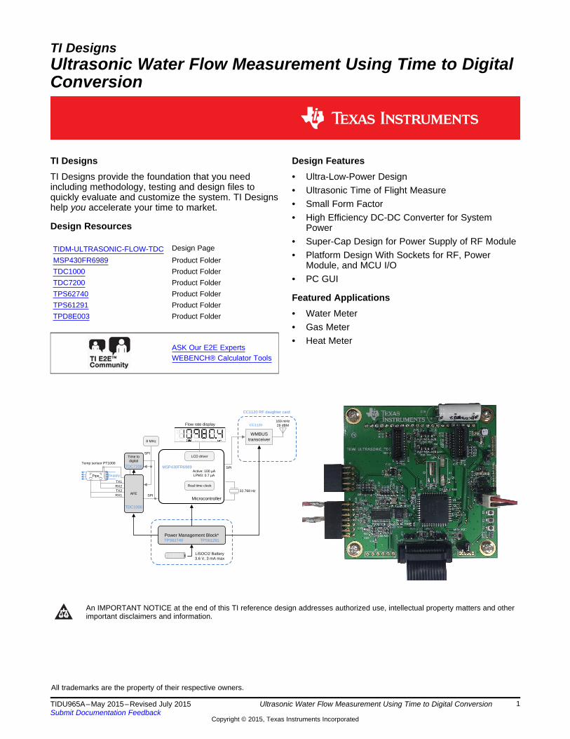
TI DesignsUltrasonic Water Flow Measurement Using Time to DigitalConversion
TI Designs Design FeaturesTI Designs provide the foundation that you need • Ultra-Low-Power Designincluding methodology, testing and design files to • Ultrasonic Time of Flight Measurequickly evaluate and customize the system. TI Designs
• Small Form Factorhelp you accelerate your time to market.• High Efficiency DC-DC Converter for System
Design Resources Power• Super-Cap Design for Power Supply of RF Module
Design PageTIDM-ULTRASONIC-FLOW-TDC• Platform Design With Sockets for RF, PowerMSP430FR6989 Product Folder Module, and MCU I/O
TDC1000 Product Folder• PC GUITDC7200 Product Folder
TPS62740 Product Folder Featured ApplicationsTPS61291 Product Folder
• Water MeterTPD8E003 Product Folder• Gas Meter• Heat Meter
ASK Our E2E ExpertsWEBENCH® Calculator Tools
An IMPORTANT NOTICE at the end of this TI reference design addresses authorized use, intellectual property matters and otherimportant disclaimers and information.
All trademarks are the property of their respective owners.
1TIDU965A–May 2015–Revised July 2015 Ultrasonic Water Flow Measurement Using Time to Digital ConversionSubmit Documentation Feedback
1 System DescriptionThis ultrasonic flow meter (water, gas, or heat meter) reference design with LCD is built using theTDC1000, TDC7200, and MSP430FR6989 (1) . The TDC chip sets measure the time of flight of ultrasonicsignals traveling in the media with an accuracy of 52 ps as the LSB of the TDC7200.
The TDC1000 is the analog front end, which transmits and receives signal. The received signal isamplified and passed to a comparator with a tunable internal reference voltage to output a sequence ofpulses called stop pulses. The TDC7200 is a high-resolution timer to measure the time of flight of signal,starting from the time at which it is transmitted from the TDC1000 to the time the stop pulses are output.
This TI design is battery powered with an ultra-low-power design. It mainly consists of the MCU, themeasurement chip set. A socket connecting the power supply circuit is provided for the RF module, whichis connected to the MCU through SPI and I/O.
Ultrasonic transducers can be directly connected to the headers J8 (see the schematic diagram) of theboard. The user can also build an external board with connectors plugged into the headers of J8 and J9.
Two DC-DC convertors are provided. The TPS62740 is used for power supply for the MCU andmeasurement system while the TPS61291 is used for the RF module. Both circuits are connected withconnectors J5 and J6.
Three push buttons are provided for users to implement more functions. This TI design is a platform baseddesign. Users can connect their own external boards to the sockets or connectors to form a highlysophisticated design.
(1) The MSP430FR6989 is used to get to the market quickly. The ESI module in this MCU is not used in this design. Evaluate theMSP430FR697x, a variant without an ESI module.
2 Ultrasonic Water Flow Measurement Using Time to Digital Conversion TIDU965A–May 2015–Revised July 2015Submit Documentation Feedback
2.1 Ultra-Low-Power DesignThe whole system consumes average current of 10.5 µA with a sampling rate of one measure per onesecond. The LCD and RF module are in an off state to reduce power consumption. This is the first versionwith a low-power design.
During the low-power mode, the system voltage is set to 2.5 V and consumes 0.5 µA. The only activecomponents during this state are the DC-DC converter TPS62740, the 32.768-KHz crystal, and the timerof the MCU. The default setting of timer is one second. Once the timer reaches the count, the systemwakes up and the system voltage generated by the TPS62740 is set to 3.3 V by the MCU.
During the active mode, power is switched on for the TDC1000 and TDC7200, which are then initializedand reset by the MCU through SPI. These chip sets will perform the measurement.
Once the measurement completed, the power supply to the TDC1000 and TDC7200 is switched off, andthe MCU enters low power mode 3 with the system voltage set to 2.5 V to lower the current consumption.
When switching the power of the devices on board to an active or low power mode state, a specificsequence and settling time is required to minimize the leakage current and the time for stabilization. Fordetails, see the short functions TDC_Chips_On() and TDC_Chips_Off() in Main.c.
2.2 Ultrasonic Measurement for Time of FlightThe basic connection of the measurement analog front end to the MCU is shown in the block diagram ofFigure 1. The TDC1000 has connections to two ultrasonic transducers. The MCU is connected to TDCchips with SPI and other control lines. During the measurement period, the MCU will power up TDC chipsand initialize them through SPI. The time of flight measurement process is done in the TDC1000 andTDC7200 without intervention of MCU. After completing the process, the measurement data is stored inthe TDC7200. The MCU will then fetch the data by SPI and switch off the TDC chip set to save power.The rest of the calculation is done in the MCU and the LCD will display the result. In this reference design,however, the MCU sends the data to the PC GUI, which will process the calculation. The MCU enters intolow power mode and will repeat the whole process after a time interval of one second (default setting).
Figure 1. Measurement Front End
3TIDU965A–May 2015–Revised July 2015 Ultrasonic Water Flow Measurement Using Time to Digital ConversionSubmit Documentation Feedback
Figure 2 shows the overview working principle of the TDC1000. The time of flight is to measure the timetaken from the transmitting transducer to the receiving transducer. In the measurement process, the MCUsends a start message through the SPI to the TDC7200, which then sends a trigger signal to theTDC1000. At the same time, the TDC1000 will send a start pulse to the TDC7200 and transmit the firstultrasonic signal through TX1 and received by RX1. This is in the same direction as the flowing media,called upstream.
In the arrival of the received signal, the TDC1000 amplifies the signal and passes it to a comparator togenerate stop pulses, which are then measured by the TDC7200 to get the time of flight of the signal.Registers of the TDC7200 containing the measurement data are then sent to the MCU through SPI forfurther processing.
To measure differential time of flight, the TDC1000 needs to repeat the same process with oppositedirection, in downstream of the flowing media, transmitting signal from TX2 and received by RX2. Thedifferential result is obtained by time taken for downstream minus that for upstream.
The transmitting pulses to a transducer are a square wave. Its frequency can be pre-defined by internalregisters of the TDC1000.
Figure 2. Time of Flight Measurement
4 Ultrasonic Water Flow Measurement Using Time to Digital Conversion TIDU965A–May 2015–Revised July 2015Submit Documentation Feedback
Maximum number of requested events (5 in this figure) returned; subsequent events not reported
Threshold
VCOM
www.ti.com Design Features
Figure 3 shows an amplified received signal of the TDC1000 with a DC bias of VCOM. The signal ispassed through a comparator with an internal reference voltage as the threshold. When the voltage of thesignal is lower than the threshold, a stop pulse is then generated when the signal crosses the VCOM. Thenumber of stop pulse can be set with the registers. However, the maximum number of stop pulsesprocessed in the TDC7200 is five. Therefore, when setting the number of pulses in the TDC1000, it has tobe equal to or larger than the number of pulses set in the TDC7200.
Figure 3. Received Signal to Stop Pulses Conversion
5TIDU965A–May 2015–Revised July 2015 Ultrasonic Water Flow Measurement Using Time to Digital ConversionSubmit Documentation Feedback
( )Time of flight Time 1 Time 2 normLSB CLOCK count 1 0.125 s= - ´ + ´ m
( )
Cal 1 normLSB offset 0.125 s
Cal 2 normLSB offset 10 0.125 s
10 1 0.125 snormLSB
Cal 2 Cal 1
´ + = m
´ + = ´ m
- ´ m=
-
Design Features www.ti.com
Figure 4 shows how the TDC7200 makes the measurement. There are 13 registers, each of which has24 bits to record the timing information. When the start pulse is generated from the TDC1000, theTDC7200 starts to measure with the external clock of 8 MHz (in this TI design). The register "Time 1" is tomeasure the time taken from the edge (polarity selectable) of the START pulse to the rising edge of the8-MHz clock. This measurement is done using the internal high resolution timer of the TDC7200 with thefine resolution of 52 ps (LSB) in average.
When the ultrasonic signal starts flying through the media in a flow meter, a timer register "CLOCK count1" is counting the number of clock cycle of 8 MHz until the first STOP pulse is received. Register "Time 2"is to measure the time taken from the edge of the first STOP pulse to the edge of the 8-MHz clock (thesame way as "Time 1"). With the information from "Time1", "CLOCK count 1", and "Time 2", the time offlight from the edge of START pulse to the edge of the first STOP pulse can be calculated.
The timer is kept running, and the received signal propagates to generate the second STOP pulse.Similarly, the same process is repeated for the second STOP pulse to obtain "CLOCK count 2" and"Time 3". The process is kept on until the fifth STOP pulse is measured.
Because there might have some deviation of high resolution timer of the TDC7200 in every measurement,the device needs calibration every time. Registers "Calibration 1" and "Calibration 2" ("Cal 1" and "Cal 2"in Figure 4, respectively) are used. In the project's default setting, Cal 1 records timing information fromthe high resolution timer in the period of 1 clock cycle of 8 MHz while Cal 2 does the same for 10 clockcycles of 8 MHz.
Equation 1 calculates the calibration of the high resolution timer as follows:
where• normLSB = normalized least significant bit• 0.125 µs = time for 1 clock cycle of 8 MHz (1)
Similar to calculating for other STOP pulses, Equation 2 calculates the time of flight for the first STOPpulse as follows:
(2)
Figure 4. Timing Registers on Five Stop Pulses
6 Ultrasonic Water Flow Measurement Using Time to Digital Conversion TIDU965A–May 2015–Revised July 2015Submit Documentation Feedback
2.3 Small Form FactorThe PCB board size is 3×3 inches, which can fit into most of the meter casing. Half of the board isoccupied with a big LCD and a socket for the RF module. The user can further reduce the board size witha smaller LCD module. The PCB area for the main chip set of the TDC1000, TDC7200, and MCU ismerely 1.1 × 2.3 inches.
2.4 High Efficiency DC-DC Converter for System Power SupplyThe TPS62740 step-down converter is used to convert 3.6 V of lithium battery into 3.3 V as systemvoltage in active mode with an efficiency up to 90%. It takes a typical quiescent current of 360 nA. Theoutput voltage is selectable. When the system is in standby mode after each measurement, the outputvoltage is set to 2.5 V to reduce overall current consumption to 0.5 µA.
2.5 Super-Cap Design for Power Supply of RF ModuleWhen an RF module is transmitting signal, a large current will be consumed. However, some lithiumbatteries have a limitation of output current. To cope with this situation, a super capacitor is used as abuffer to store the charges from the battery and to supply large current for the use of RF power amplifier.
In the daily operation of a flow meter, the RF module is only switched on for a short time to send out thereading of the meter to the data concentrator, a few times per day or per week. In the standby mode, themodule is switched off to save power. During the standby mode, the super capacitor is charged up to2.5 V. In transmitting mode, a boost converter (TPS61291) connecting to the super cap is enabled to stepup the output voltage to 3.3 V, which will supply the power to RF module. All the current used in the RFmodule will then only be taken from the supper capacitor.
2.6 Platform DesignThe board is designed with a platform-based concept. It has the core function of measurement unit and anMCU with an LCD module. The board also has reserved some sockets for adding on extra functionalitiesor circuit modification.
One important socket is the RF socket, which is connected to the SPI and I/O port of the MCU and has adedicated power supply module. This socket can plug in with the communication module, like Wi-Fi,Bluetooth, or M-bus of a wired or wireless type. It also can be used as an extended connection to otherdevice modules.
The power supply module can be modified with the sockets connecting to it. The user can remove thepower components and replace it with a new module connecting to the sockets.
While programming the MCU, the user can select the JTAG interface or the Spy-Bi-Wire connection. Inthe socket of the Spy-Bi-Wire, it uses a six-pin socket with a UART pin directly connected to MCU. Thissocket is compatible with the eZ-FET tool of the MSP430.
2.7 PC GUIA PC GUI is provided to control the operation of the system. This GUI has the panel for the TDC1000 andTDC7200 set up. It can monitor the time of flight for each STOP pulse. The GUI has reserved some otherfunctions like the flow rate and temperature sensing. However, the first version of the MCU firmware hasnot been implemented with these functions yet.
7TIDU965A–May 2015–Revised July 2015 Ultrasonic Water Flow Measurement Using Time to Digital ConversionSubmit Documentation Feedback
This solution of the ultrasonic flow meter is built on the TDC1000, TDC7200, and the MCUMSP430FR6989 with an LCD display soldered on the bottom size of the board. This board is powered bya 3.6-V lithium battery, which is down converted to 3.3 V through a voltage selectable buck converter ofthe TPS62740. For the operation of this board, it can be descripted with 15 parts controlled with the MCU.Details follow for each part:1. An external board can be built and plugged into this socket and the socket of Part 2 to enhance its
features.
Figure 7. Socket (J9) Connecting to I/O of MCU
9TIDU965A–May 2015–Revised July 2015 Ultrasonic Water Flow Measurement Using Time to Digital ConversionSubmit Documentation Feedback
2. Ultrasonic transducers are to be connected through this socket.J8 also provides two pin sockets for external temperature sensors connecting RTD1 and RTD2 signalsin the circuit. These signals are used when temperature of the media in a meter is included for themeasurement, like heat meters.
Figure 8. Socket (J8) Connecting Transmitting and Receiving Pins of TDC1000
3. space
Figure 9. Jumpers JP2 and JP3 Connect Onboard LED
4. A slot of test pins for START and STOP pulses, VCOM, and the internal input of the comparator in theTDC1000.
Figure 10. Test Pins of TDC1000
5. Pins 12 and 14 of this header are connected to the UART pin of the MCU. Use the latest MSP430 FETTool with the UART feature to connect the board to the PC GUI. When using external power, the VCCof the MCU has to be connected to pin 4 of the JTAG; the user can select either the TARGET_3V3 orVBAT.
Figure 11. JTAG Interface for MSP430 FET Tool to Program MCU
10 Ultrasonic Water Flow Measurement Using Time to Digital Conversion TIDU965A–May 2015–Revised July 2015Submit Documentation Feedback
6. This interface is compatible with the eZ-FET tool of the MSP430. Use the UART feature of the eZ-FETto connect the board to the PC GUI.
Figure 12. Spy-Bi-Wire and UART Interface
7. When using the eZ-FET tool and needing the power supplied from it, short this jumper and pins 1 and2 of jumper J4 located in Part 11.
Figure 13. Jumper JP1
8. space
Figure 14. MCU Reset Button
9. Use these buttons to add on new features. There is no implementation for these buttons in thefirmware. To operate this circuit: when a push button is pressed, it pulls the voltage of the "BUT_AN" tolow to trigger an interrupt routine, which then switches on the ADC to measure the input voltage todetermine which button is pressed.
Figure 15. Three Push Buttons (Reserved for Future Use)
11TIDU965A–May 2015–Revised July 2015 Ultrasonic Water Flow Measurement Using Time to Digital ConversionSubmit Documentation Feedback
10. When battery is used, pins 2 and 3 of J4 are shorted with jumper and JP1 is opened.The jumper JP5 (see Figure 17) near the connector is to short the capacitor C17 to provide an alwayspull-up resistor to pin VSEL2 of the TPS62740, which will then output 2.0 V to start the MCU. Use it asan easy circuit setting of voltage selection during development of new firmware. To use this jumper,the MCU pin connecting to it has to be set as input mode. Once developed, remove the jumper to savecurrent consumption.
Figure 16. Battery Connector Using 3.6-V Lithium Battery
11. When connected to a battery, a low-power circuit consisting of C17 and R15 is used to provide a pulseto VSEL4, a selection pin of the TPS62740, to select an initial voltage of 2.6 V, which is high enough tostart the MCU.In the initialization of the firmware, it has to select the proper operation voltage by using the selectionpins.If all pins are pulled to low, the output voltage of 1.8 V may not be high enough to start the MCU. Inthis situation, short the input and output of the U3 (TPS62740) to supply 3.x V to the MCU and re-program it with proper firmware.There is a header (J6) connecting to each pin of U3.
Figure 17. Buck Converter Using TPS62740 to Provide VCC to the System
12 Ultrasonic Water Flow Measurement Using Time to Digital Conversion TIDU965A–May 2015–Revised July 2015Submit Documentation Feedback
12. The firmware does not implement this part, as this is reserved for future use.A dedicated power supply for Part 14. When the communication module connecting to Part 14 isturned on, a large current will be given out by the super capacitor and the voltage will be stepped up to3.3 V. The design will isolate the communication power from the system power. The design will nothave current flowing from the system power to the module during its active state.
Figure 18. Boost Converter With Super Capacitor (in Part 13)
13. The firmware does not implement this part, as this is reserved for future use.Operation is as follows: A super capacitor, which is charged up from the battery through an npn switchand resistor (located in the middle of Part 14) to 2.5 V. This is done when the communication moduleconnecting to Part 14 is in standby mode. When the module is in active mode, the npn switch will beturned off to isolate the battery power.There are two charging circuits. When the super cap is empty or with very little charges,"SLOW_CHARGE" is high and the circuit will charge up the super capacitor with current= (V2.5 – V_SUP_CAP) / 2.4k, which will limit the current to below 1 mA. This limitation is necessary,as the lithium battery has a limited current output.When the super cap is 0.1 V lower than V2.5, a resistor of 100 Ω is used instead of 2.4 K; the circuit isnamed "FAST_CHARGE". Every time a communication module is activated, it only consumes somecharges in the super capacitor to lower its voltage within 0.1 V. Therefore, "FAST_CHARGE" will beused to re-charge the super-cap for the next communication use.
Figure 19. Resistive Charging Circuit for Super Capacitor
13TIDU965A–May 2015–Revised July 2015 Ultrasonic Water Flow Measurement Using Time to Digital ConversionSubmit Documentation Feedback
14. The socket has connection of SPI, UART and GPIO to the MCU. The user can also plug in anextension board to enhance the system features.The "V_PA" is the power supply for the power amplifier of the RF module. For testing, jumper JP4(see Figure 16) is provided to direct connection to the DC or battery power supply.
Figure 20. Socket for Connection of Communication Module (Wired or Wireless Type)
14 Ultrasonic Water Flow Measurement Using Time to Digital Conversion TIDU965A–May 2015–Revised July 2015Submit Documentation Feedback
15. The core circuit of measurement on this TI design consists of the TDC1000, TDC7200 and an 8-MHzoscillator. Some important notes as follows have to be followed when implementing this circuit.The ferrite in FB1 and FB2 with capacitors of 0.1 µF and 0.01 µF, respectively, are used to provide alow-noise DC power to the TDC1000. When implementing the low-power design, AVDD and VIO to theTDC1000 are connected together. From the datasheet, AVDD must be set to be equal to or higherthan VIO; otherwise, a large current of a couple of mA will be drained. When in standby mode, both theTDC1000 and TDC7200 will be disabled by pulling low the enable pin.
Figure 21. Low-Pass Filters for Power Supplies of TDC1000
The stability of VCOM is important for accurate measurement. 10 nF in C24 is used; by experiment, itis the most optimal value. The R52 is used as a reference resistor for measurement of temperaturesensor PT500 / PT1000. The accuracy of this 1-KΩ resistor is 0.01%.Resistors R40 and R57 are used to provide damping of ultrasonic transducers. With these resistors,the difference of differential time of flight among STOP1 to STOP5 is reduced.The following circuit from "PGAOUT" to "COMPIN" is to provide a band pass filter with centerfrequency of 1 MHz to reduce noise of the received signal. As a result, the standard deviation ofmeasurement data is reduced.
Figure 22. Critical External Passive Circuits of TDC1000
15TIDU965A–May 2015–Revised July 2015 Ultrasonic Water Flow Measurement Using Time to Digital ConversionSubmit Documentation Feedback
The R43 and R45 of 200 Ω have to be matched with each other within a 1% error; so for the capacitorsC32 and C33. As the measurement on the differential time of flight is in unit of picosecond, to reduceoffset value, the length of signal lines on transmitting end and receiving end have to be matched. Forthe same reason, the START and STOP signal lines need to be matched as well.
Figure 23. PCB Layout of Matched Signal Lines
16 Ultrasonic Water Flow Measurement Using Time to Digital Conversion TIDU965A–May 2015–Revised July 2015Submit Documentation Feedback
The software is designed to optimize the power consumption of the system. It starts with initializing theMCU peripherals and I/O ports. The flowchart shown in Figure 24 consists of the PC GUI operation. In theinfinite loop of measurement, it checks the command from the GUI and then triggers the measurement. Asthe TDC1000 and TDDC7200 are powered off in standby mode, when they are powered on, the registersetting has to be reloaded. The whole process of power on, measurement, and power off need a period ofaround 35 ms in which a large portion is the delay for stabilization of the system. After that, readings fromthe TDC7200 are sent to the GUI through UART. The MCU will enter into a low-power mode and wait for1 second in default before the next cycle of measurement.
In the software, two modes can be selected. One mode is working with the GUI and another is without theGUI. The mode can be selected with "define GUI" in "global.h". Remark it to select non-GUI operation,which will use the minimum power consumption. For both GUI and NON-GUI operation, the LCD willdisplay the differential time of flight.
17TIDU965A–May 2015–Revised July 2015 Ultrasonic Water Flow Measurement Using Time to Digital ConversionSubmit Documentation Feedback
6 PC GUI OperationIn the GUI, only five pages or TABs are used: SETUP, TDC1000, TDC7200, TOF_ONE_SHOT, andGRAPH. Raw data from the TDC7200 will be sent to the GUI and processed. There is no calculated resultin the firmware.
In the SETUP tab, select the com port connecting to the board and click "CONNECT" to link the board andthe PC GUI.
The triggering frequency is defaulted to 1 second in the firmware. The user can select the triggeringfrequency on this page. However, do not select 100 ms because there may not be enough time to synchthe data stream/GUI command to the firmware and the GUI.
Figure 25. SETUP Settings
18 Ultrasonic Water Flow Measurement Using Time to Digital Conversion TIDU965A–May 2015–Revised July 2015Submit Documentation Feedback
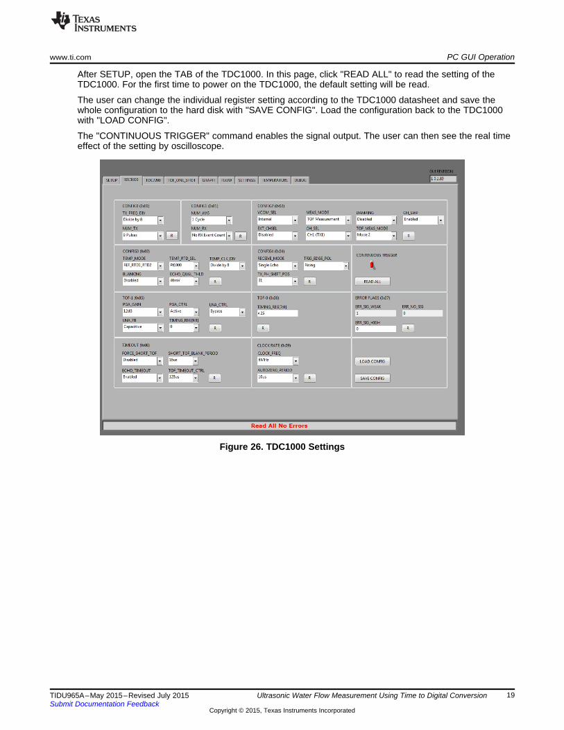
After SETUP, open the TAB of the TDC1000. In this page, click "READ ALL" to read the setting of theTDC1000. For the first time to power on the TDC1000, the default setting will be read.
The user can change the individual register setting according to the TDC1000 datasheet and save thewhole configuration to the hard disk with "SAVE CONFIG". Load the configuration back to the TDC1000with "LOAD CONFIG".
The "CONTINUOUS TRIGGER" command enables the signal output. The user can then see the real timeeffect of the setting by oscilloscope.
Figure 26. TDC1000 Settings
19TIDU965A–May 2015–Revised July 2015 Ultrasonic Water Flow Measurement Using Time to Digital ConversionSubmit Documentation Feedback
In the TAB of the TDC7200, the user can configure the register setting of the TDC7200. At the first time ofpower up and "READ ALL" is clicked, the default setting of TDC7200 is read.
The user can configure individual register settings according to the TDC7200 datasheet. "SAVE CONFIG"to save the setting into hard disk. "LOAD CONFIG" to load the setting from hard disk into the registers.
Figure 27. TDC7200 Settings
20 Ultrasonic Water Flow Measurement Using Time to Digital Conversion TIDU965A–May 2015–Revised July 2015Submit Documentation Feedback
In the TAB of "GRAPH", it receives the streaming data from the TI design. After calculation, the result isdisplayed onto the monitor in black.
The GUI has the function of saving the graph data and records the register readings into a file. To enablethis function, the corresponding check box is selected. When the "FLOW MODE" is checked, thedifferential time of flight will be displayed.
When the "FLOW MODE" is unchecked, the time of flight from the START pulse to the STOP pulse isdisplayed.
"TDC_SELECT" to select different STOP pulse, from STOP 1 to STOP 5 in "START GRAPH" is clicked tostart the data logging. "STOP GRAPH" is to stop the data logging.
If the reading is out of scale, move the mouse cursor to the black monitor and right click. Select"Auto Scale Y" to auto scale the curve into the right position.
Figure 29. GRAPH Settings
22 Ultrasonic Water Flow Measurement Using Time to Digital Conversion TIDU965A–May 2015–Revised July 2015Submit Documentation Feedback
Figure 30. System Setup to Measure Accuracy of Differential Time of Flight
The setup includes an ultrasonic pipe filled with water connected to the board, as shown in Figure 30. Thepipe is sealed at both ends without the flow of water to measure the accuracy of the differential time offlight of the system. The procedure is as follows:1. Remove all jumpers.2. Connect pin 2 and 3 of J4.3. Connect ultrasonic transducers in a pipe filled with water to J8.4. Connect UART in JTAG interface, or using UART connection in J15. Plug in the 3.6-V DC supply to J3.6. Switch on the DC power supply.7. Program it using Code Composer Studio™ (CCS) 6.1, with the firmware which defines PC GUI by
using "#define OPERATION_MODE 2" in "global.h". After that, exit CCS.8. Press the MCU reset button to ensure a restart of the firmware.9. Open the PC GUI.10. Select the proper COM port in SETUP page of the GUI and click "CONNECT".11. Select "1 second" as triggering frequency.12. In TDC1000 TAB, click "READ ALL" to load the default setting from the firmware.13. In TDC7200 TAB, click "READ ALL" to load the default setting from the firmware.14. In the "GRAPH" TAB, check "FLOW MODE" to measure the differential time of flight.15. Check the box of "SAVE RESULT REGR TOFILE".16. Click "START GRAPH".17. A window is displayed. Enter the file name of the file and click "OK".18. Wait for five minutes and click "Stop Graph".19. Process the data of the file using Microsoft® Excel®.
23TIDU965A–May 2015–Revised July 2015 Ultrasonic Water Flow Measurement Using Time to Digital ConversionSubmit Documentation Feedback
Figure 31. System Setup to Measure of Current Consumption
This setup uses an eZ-FET tool with EnergyTrace™ module to monitor the energy consumption of the TIdesign. This tool uses a Spy-Bi-Wire connection. The UART has to be disconnected to avoid currentleakage. This setup includes an ultrasonic pipe filled with water connected to the board. The setupprocedure is as follows:1. Remove all jumpers, DC power, and JTAG connection.2. Short the jumper JP1 and short pin 1 and 2 of J4.3. Connect the Spy-Bi-Wire from the eZ-FET to J1 on the board, without connecting the UART pins.4. Connect eZ-FET to PC.5. Program the it using CCS 6.1, with the firmware without PC GUI and LCD, by using
"#define OPERATION_MODE 1" in "global.h".6. Compile and enter debug mode of CCS.7. In the "EnergyTrace" setting panel in CCS 6, set 10 second as the measurement duration.8. Select "Run" in menu bar and click "Free Run".9. Click the "Energy" tab in "EnergyTrace" panel.10. The user can see a large surge of energy in the beginning of initialization of the firmware.11. Press "ALT + F8" to suspend the program.12. Select "Run" in menu bar and click "Free Run" again.13. The energy consumption in steady state is shown on the "EnergyTrace" monitor.14. Click the "EnergyTrace Technology" tab to read the energy consumption and supply voltage. With this
data, the average current consumption can be calculated.
24 Ultrasonic Water Flow Measurement Using Time to Digital Conversion TIDU965A–May 2015–Revised July 2015Submit Documentation Feedback
8 Test ResultsThe test results for accuracy are shown in Figure 32 and Figure 33. Figure 32 shows the plot of thedifferential time of flight for each STOP pulse over five minutes time, with one measure per second.Figure 33 shows the average of these five curves. Table 1 shows the mean value and the standarddeviation of the results.
From Table 1, the mean value is supposed to be zero for a zero flow rate. However, it comes out as asignificant figure. This difference is due to the imbalance of transducers and unmatched value of the frontend components. As it represents a zero flow, the mean value can be treated as an offset in thecalculation of the flow rate.
The standard deviation for each STOP is ranged from 134 to 241 ps, while that of the averaged data isonly 126 ps. Implement a higher accuracy system by taking a couple of measures per second and performaveraging technique to reduce error (standard deviation).
Table 1. Mean and Standard Deviation of the Test Results
DIFFERENTIAL TOF MEAN VALUE STANDARD DEVIATIONSTOP1 –2.934 ns 241 psSTOP2 –2.928 ns 205 psSTOP3 –2.521ns 153 psSTOP4 –2.200 ns 134 psSTOP5 –1.806 ns 157 ps
Averaged curve –2.478 ns 126 ps
Figure 32. Test Results of Five STOPs
Figure 33. Test Results of the Average of Five STOPs
25TIDU965A–May 2015–Revised July 2015 Ultrasonic Water Flow Measurement Using Time to Digital ConversionSubmit Documentation Feedback
Figure 34 shows the pattern of energy consumption. A low power mode with a system voltage of 2.5 V isthe normal state. When a one-second time interval is reached, the MCU sets the system voltage to 3.3 Vand wakes up the system for measurement. During the active period of 2.2 ms, a comparatively largecurrent is consumed, which reflects in a step increment in the energy consumption in the graph. Aftermeasurement, the MCU switches off the system to low power mode and set the voltage to 2.5 V from3.3 V. During this state, the charges in the output capacitor of the TPS62740 provide the current intake ofthe system, which almost does not need any extra charges from the supply and so the curve is flat.
The calculation of average current is as follows:
The total energy consumed in 10 seconds = 375 µJThe voltage supply from the eZ-FET is 3.58 VTherefore the average current consumption = 375 / 10 / 3.58 = 10.5 µA
Figure 34. Energy Consumption of TI Design
26 Ultrasonic Water Flow Measurement Using Time to Digital Conversion TIDU965A–May 2015–Revised July 2015Submit Documentation Feedback
RX pins. Place minimal parasiticcapacitances onto RX1&RX2
Interstage Passive Filters:
Configured for 1 MHz
AGND
TX1
TX2
RX1
RX2
TX2/RX1or TX2
0
R55
TX2/RX1or RX1
0R56
TX1/RX2 or TX1
TX1/RX2 or RX2
200
R43
200
R45
1
3
5 6
4
2
7
9 10
8
1211
1413
J8
RTD1RTD2
1000pFC26
51pFC23
1.00k
R47
51pFC25
AGND
RTD2
RTD1
AGND
1.00k
R52
AGND
VCOM
ST
AR
T
ST
OP
5.36k
R44 VCOM
TDC1000_ENABLE
TDC1000_ ERRB
TDC1000_CHSEL
TDC1000_RESET
MSP430_TRIGGER
TDC7200_TRIGGER
0.01µFC28
AGND
0.1µFC29
AGND
V3p3
GND
OSC_OUT
AVDD
CLK
CPU_CLK_OUT
33R61
60 ohm
FB1
GND
0.01µF
C34
OSC_ENABLE
0.01µF
C30
GND
0.1µF
C31
GND
V3p3
SPI_MISOTRIGGER_IN
33R58
SPI_MOSI
SPI_SCLK
TDC1000_SPI_CSB
10.0kR54
10.0kR53
CO
MP
IN
Place filter capsto VDD pins
Directly connected STOP and START traces fromTDC71000 to TDC7200 must be completelysymmetrical and as short as possible to avoidintroducing timing delay
Pin 1 and pin 14 of the connectormust be marked on the PC board
All the labels appearing on pin 2, 4, 6, 8, 10,12 and 14 must be marked on the PC board
VDD_TDC1000
VIO
10.0MegR48
AGND
10.0MegR50
60 ohm
FB2
STOP
START
0.01µF
C24
VDD4
STANDBY1
GND2
OUT3
8MHz
Y1
ASEMB-8.000MHZ-LY-T
AVDD
0.1µF
C3560 ohm
FB3
CLK
10µFC27
AGND
RX
11
RX
22
VC
OM
3
LN
AO
UT
4
PG
AIN
5
PG
AO
UT
6
CO
MP
IN7
RT
D1
8
RT
D2
9
RR
EF
10
CH
SE
L11
ER
RB
12
ST
AR
T13
ST
OP
14
EN
15
TR
IGG
ER
16
RE
SE
T17
SC
LK
18
CS
B19
SD
I20
SD
O21
VIO
22
VD
D23
VD
D24
CLK
IN25
GN
D26
TX
227
TX
128
U5TDC1000PW
GPIO7
GPIO5
GPIO6
GPIO4
TDC1000_CHSEL
GPIO2
GPIO1
GPIO3
1
3
56
4
2
7
910
8
J9
PPPC052LJBN-RC
GPIO2
GPIO3
GPIO1
GPIO4
GPIO5
TDC1000_CHSEL
GPIO6
GPIO7
GND
GND
Pin 1 and pin 10 of the connectormust be marked on the PC board
IO11
IO22
IO33
IO44
IO5 5
IO6 6
IO77
IO88
EP9
U6
TPD8E003DQDR
VS
5
4
1
2
3
6
J7
GND
AGND
STOPSTARTCOMPIN
VCOM
DNP R60
DNP R63
100KR46
100K
R42
IM_CH2_SEL
3
1
2
Q5
MMBT3904
100KR51
100K
R49
IM_CH1_SEL
3
1
2
Q6MMBT3904
TX1
TX2
510
R40
510R57
AGND
AGND
AGND
AGND
AGND
10MR59
DNPR62
www.ti.com Design Files
9 Design Files
9.1 SchematicsTo download the schematics, see the design files at TIDM-ULTRASONIC-FLOW-TDC.
Figure 35. TDC1000 Schematic
27TIDU965A–May 2015–Revised July 2015 Ultrasonic Water Flow Measurement Using Time to Digital ConversionSubmit Documentation Feedback
9.4 Altium Project FilesTo download the Altium project files, see the design files at TIDM-ULTRASONIC-FLOW-TDC.
9.5 Gerber FilesTo download the Gerber files, see the design files at TIDM-ULTRASONIC-FLOW-TDC.
9.6 Software FilesTo download the software files, see the design files at TIDM-ULTRASONIC-FLOW-TDC.
9.7 RF ModulesFor more information on RF modules, contact Milen Stefanov at [email protected].
10 About the AuthorTHOMAS KOT is a system and solutions architect in the Smart Grid and Energy group at TexasInstruments, where he primarily works on the flow meter reference design development and customersupport. Thomas received his bachelor of engineering in electronic engineering from Hong KongPolytechnic University in 1995 and received his master of science in electronic and informationengineering from the same university in 2005. He received the master of business administration from CityUniversity of Hong Kong in 2007. Contact Thomas at [email protected].
36 Ultrasonic Water Flow Measurement Using Time to Digital Conversion TIDU965A–May 2015–Revised July 2015Submit Documentation Feedback
Changes from Original (May 2015) to A Revision ........................................................................................................... Page
• Changed title from Ultrasonic TDC Flowmeter Reference Design.................................................................. 1
NOTE: Page numbers for previous revisions may differ from page numbers in the current version.
37TIDU965A–May 2015–Revised July 2015 Revision HistorySubmit Documentation Feedback
Texas Instruments Incorporated ("TI") reference designs are solely intended to assist designers (“Buyers”) who are developing systems thatincorporate TI semiconductor products (also referred to herein as “components”). Buyer understands and agrees that Buyer remainsresponsible for using its independent analysis, evaluation and judgment in designing Buyer’s systems and products.TI reference designs have been created using standard laboratory conditions and engineering practices. TI has not conducted anytesting other than that specifically described in the published documentation for a particular reference design. TI may makecorrections, enhancements, improvements and other changes to its reference designs.Buyers are authorized to use TI reference designs with the TI component(s) identified in each particular reference design and to modify thereference design in the development of their end products. HOWEVER, NO OTHER LICENSE, EXPRESS OR IMPLIED, BY ESTOPPELOR OTHERWISE TO ANY OTHER TI INTELLECTUAL PROPERTY RIGHT, AND NO LICENSE TO ANY THIRD PARTY TECHNOLOGYOR INTELLECTUAL PROPERTY RIGHT, IS GRANTED HEREIN, including but not limited to any patent right, copyright, mask work right,or other intellectual property right relating to any combination, machine, or process in which TI components or services are used.Information published by TI regarding third-party products or services does not constitute a license to use such products or services, or awarranty or endorsement thereof. Use of such information may require a license from a third party under the patents or other intellectualproperty of the third party, or a license from TI under the patents or other intellectual property of TI.TI REFERENCE DESIGNS ARE PROVIDED "AS IS". TI MAKES NO WARRANTIES OR REPRESENTATIONS WITH REGARD TO THEREFERENCE DESIGNS OR USE OF THE REFERENCE DESIGNS, EXPRESS, IMPLIED OR STATUTORY, INCLUDING ACCURACY ORCOMPLETENESS. TI DISCLAIMS ANY WARRANTY OF TITLE AND ANY IMPLIED WARRANTIES OF MERCHANTABILITY, FITNESSFOR A PARTICULAR PURPOSE, QUIET ENJOYMENT, QUIET POSSESSION, AND NON-INFRINGEMENT OF ANY THIRD PARTYINTELLECTUAL PROPERTY RIGHTS WITH REGARD TO TI REFERENCE DESIGNS OR USE THEREOF. TI SHALL NOT BE LIABLEFOR AND SHALL NOT DEFEND OR INDEMNIFY BUYERS AGAINST ANY THIRD PARTY INFRINGEMENT CLAIM THAT RELATES TOOR IS BASED ON A COMBINATION OF COMPONENTS PROVIDED IN A TI REFERENCE DESIGN. IN NO EVENT SHALL TI BELIABLE FOR ANY ACTUAL, SPECIAL, INCIDENTAL, CONSEQUENTIAL OR INDIRECT DAMAGES, HOWEVER CAUSED, ON ANYTHEORY OF LIABILITY AND WHETHER OR NOT TI HAS BEEN ADVISED OF THE POSSIBILITY OF SUCH DAMAGES, ARISING INANY WAY OUT OF TI REFERENCE DESIGNS OR BUYER’S USE OF TI REFERENCE DESIGNS.TI reserves the right to make corrections, enhancements, improvements and other changes to its semiconductor products and services perJESD46, latest issue, and to discontinue any product or service per JESD48, latest issue. Buyers should obtain the latest relevantinformation before placing orders and should verify that such information is current and complete. All semiconductor products are soldsubject to TI’s terms and conditions of sale supplied at the time of order acknowledgment.TI warrants performance of its components to the specifications applicable at the time of sale, in accordance with the warranty in TI’s termsand conditions of sale of semiconductor products. Testing and other quality control techniques for TI components are used to the extent TIdeems necessary to support this warranty. Except where mandated by applicable law, testing of all parameters of each component is notnecessarily performed.TI assumes no liability for applications assistance or the design of Buyers’ products. Buyers are responsible for their products andapplications using TI components. To minimize the risks associated with Buyers’ products and applications, Buyers should provideadequate design and operating safeguards.Reproduction of significant portions of TI information in TI data books, data sheets or reference designs is permissible only if reproduction iswithout alteration and is accompanied by all associated warranties, conditions, limitations, and notices. TI is not responsible or liable forsuch altered documentation. Information of third parties may be subject to additional restrictions.Buyer acknowledges and agrees that it is solely responsible for compliance with all legal, regulatory and safety-related requirementsconcerning its products, and any use of TI components in its applications, notwithstanding any applications-related information or supportthat may be provided by TI. Buyer represents and agrees that it has all the necessary expertise to create and implement safeguards thatanticipate dangerous failures, monitor failures and their consequences, lessen the likelihood of dangerous failures and take appropriateremedial actions. Buyer will fully indemnify TI and its representatives against any damages arising out of the use of any TI components inBuyer’s safety-critical applications.In some cases, TI components may be promoted specifically to facilitate safety-related applications. With such components, TI’s goal is tohelp enable customers to design and create their own end-product solutions that meet applicable functional safety standards andrequirements. Nonetheless, such components are subject to these terms.No TI components are authorized for use in FDA Class III (or similar life-critical medical equipment) unless authorized officers of the partieshave executed an agreement specifically governing such use.Only those TI components that TI has specifically designated as military grade or “enhanced plastic” are designed and intended for use inmilitary/aerospace applications or environments. Buyer acknowledges and agrees that any military or aerospace use of TI components thathave not been so designated is solely at Buyer's risk, and Buyer is solely responsible for compliance with all legal and regulatoryrequirements in connection with such use.TI has specifically designated certain components as meeting ISO/TS16949 requirements, mainly for automotive use. In any case of use ofnon-designated products, TI will not be responsible for any failure to meet ISO/TS16949.IMPORTANT NOTICE