SANDIA REPORT SAND2010-7213 Unlimited Release Printed November 2010 Ultrathin Coatings of Nanoporous Materials as Property Enhancements for Advanced Functional Materials Eric N. Coker Prepared by Sandia National Laboratories Albuquerque, New Mexico 87185 and Livermore, California 94550 Sandia National Laboratories is a multi-program laboratory managed and operated by Sandia Corporation, a wholly owned subsidiary of Lockheed Martin Corporation, for the U.S. Department of Energy's National Nuclear Security Administration under contract DE-AC04-94AL85000. Approved for public release; further dissemination unlimited.
Transcript
SANDIA REPORT SAND2010-7213 Unlimited Release Printed November 2010
Ultrathin Coatings of Nanoporous Materials as Property Enhancements for Advanced Functional Materials Eric N. Coker Prepared by Sandia National Laboratories Albuquerque, New Mexico 87185 and Livermore, California 94550
Sandia National Laboratories is a multi-program laboratory managed and operated by Sandia Corporation, a wholly owned subsidiary of Lockheed Martin Corporation, for the U.S. Department of Energy's National Nuclear Security Administration under contract DE-AC04-94AL85000. Approved for public release; further dissemination unlimited.
2
Issued by Sandia National Laboratories, operated for the United States Department of Energy by Sandia Corporation. NOTICE: This report was prepared as an account of work sponsored by an agency of the United States Government. Neither the United States Government, nor any agency thereof, nor any of their employees, nor any of their contractors, subcontractors, or their employees, make any warranty, express or implied, or assume any legal liability or responsibility for the accuracy, completeness, or usefulness of any information, apparatus, product, or process disclosed, or represent that its use would not infringe privately owned rights. Reference herein to any specific commercial product, process, or service by trade name, trademark, manufacturer, or otherwise, does not necessarily constitute or imply its endorsement, recommendation, or favoring by the United States Government, any agency thereof, or any of their contractors or subcontractors. The views and opinions expressed herein do not necessarily state or reflect those of the United States Government, any agency thereof, or any of their contractors. Printed in the United States of America. This report has been reproduced directly from the best available copy. Available to DOE and DOE contractors from U.S. Department of Energy Office of Scientific and Technical Information P.O. Box 62 Oak Ridge, TN 37831 Telephone: (865) 576-8401 Facsimile: (865) 576-5728 E-Mail: [email protected] Online ordering: http://www.osti.gov/bridge Available to the public from U.S. Department of Commerce National Technical Information Service 5285 Port Royal Rd. Springfield, VA 22161 Telephone: (800) 553-6847 Facsimile: (703) 605-6900 E-Mail: [email protected] Online order: http://www.ntis.gov/help/ordermethods.asp?loc=7-4-0#online
3
SAND2010-7213 Unlimited Release
Printed November 2010
Ultrathin Coatings of Nanoporous Materials as Property Enhancements for Advanced Functional Materials
Eric N. Coker Ceramic Processing & Inorganic Materials
Sandia National Laboratories P.O. Box 5800
Albuquerque, New Mexico 87185-1349
Abstract
This report summarizes the findings of a five-month LDRD project funded through Sandia’s NTM Investment Area. The project was aimed at providing the foundation for the development of advanced functional materials through the application of ultra-thin coatings of microporous or mesoporous materials onto the surface of substrates such as silicon wafers. Prior art teaches that layers of microporous materials such as zeolites may be applied as, e.g., sensor platforms or gas separation membranes. These layers, however, are typically several microns to several hundred microns thick. For many potential applications, vast improvements in the response of a device could be realized if the thickness of the porous layer were reduced to tens of nanometers. However, a basic understanding of how to synthesize or fabricate such ultra-thin layers is lacking. This report describes traditional and novel approaches to the growth of layers of microporous materials on silicon wafers. The novel approaches include reduction of the quantity of nutrients available to grow the zeolite layer through minimization of solution volume, and reaction of organic base (template) with thermally-oxidized silicon wafers under a steam atmosphere to generate ultra-thin layers of zeolite MFI.
4
ACKNOWLEDGEMENTS This project was funded by Sandia National Laboratories’ Laboratory Directed Research and Development (LDRD) office, under the Nano-to-Micro initiative. Thanks to Kristin Meyer (STAR high-school student) and Kathy Huang (ACTS visiting high-school teacher) who helped with zeolite synthesis during the summer. Thanks to Bonnie McKenzie (org 01822) for imaging the samples using Scanning Electron Microscopy.
2. Experimental Section ................................................................................................................. 9 2.1. Synthesis of zeolite layers by traditional hydrothermal methods ................................... 9 2.2. Synthesis of zeolite layers by novel methods ............................................................... 10
2.2.1. Volume-minimization ..................................................................................... 10 2.2.2. Layer growth by partial conversion of silicon wafer ...................................... 10
2.3. Characterization of zeolite layers .................................................................................. 11
3. Results and discussion ............................................................................................................. 15 3.1. Synthesis of zeolite layers by traditional hydrothermal methods ................................. 15
3.1.1. Effect of wafer cleaning method ..................................................................... 25 3.2. Synthesis of zeolite layers by novel methods ............................................................... 26
3.2.1. Volume-minimization ..................................................................................... 26 3.2.2. Layer growth by partial conversion of silicon wafer ...................................... 28
Distribution ................................................................................................................................... 36
FIGURES Figure 1. Schematic representation of a reactor used to grow zeolite layers on silicon wafers by the conventional immersion method using excess reactant solution volume. ................................ 9 Figure 2. Schematic representation of a reactor used to grow zeolite layers on silicon wafers using reduced reactant solution volume, and with the wafer oriented horizontally above a liquid layer............................................................................................................................................... 11 Figure 3. Typical XRD pattern of a powder sample collected from a Teflon-lined reactor after growth of zeolite layers on silicon wafers. ................................................................................... 15 Figure 4. Representation of a crystal of zeolite MFI. Straight pores run parallel to the b-axis (shortest crystal dimension), while sinusoidal pores run along the a- and c-axes. The dashed lines indicate the angular c-axis termination observed in some of the syntheses described below........................................................................................................................................................ 16 Figure 5. XRD pattern (upper) and SEM image (lower) of sample 1-66E, zeolite MFI layer on silicon wafer. The principal 0 k 0 peaks indicative of an aligned layer are labeled in the XRD pattern. In addition, the multiple h k l cluster of overlapping peaks is indicated, as are the peaks due to the silicon substrate (*). ..................................................................................................... 17 Figure 6. XRD pattern (upper) and SEM image (lower) of sample 1-57E, zeolite MFI layer on silicon wafer. For XRD peak assignments, refer to Figure 5....................................................... 18 Figure 7. XRD pattern (upper) and SEM image (lower) of sample 1-6-2, zeolite MFI layer on silicon wafer. For XRD peak assignments, refer to Figure 5....................................................... 19 Figure 8. XRD pattern (upper) and SEM image (lower) of sample 1-68A, zeolite MFI layer on silicon wafer. For XRD peak assignments, refer to Figure 5....................................................... 20
6
Figure 9. XRD pattern (upper) and SEM image (lower) of sample 1-70A, zeolite MFI layer on silicon wafer. For XRD peak assignments, refer to Figure 5....................................................... 22 Figure 10. XRD pattern (upper) and SEM image (lower) of sample 1-67A, zeolite MFI layer on silicon wafer. For XRD peak assignments, refer to Figure 5....................................................... 24 Figure 11. XRD pattern (upper) and SEM image (lower) of sample 1-70C, zeolite MFI layer on silicon wafer. For XRD peak assignments, refer to Figure 5....................................................... 25 Figure 12. XRD pattern (upper) and SEM image (lower) of sample 1-81A2, zeolite MFI layer on silicon wafer. ................................................................................................................................. 27 Figure 13. XRD pattern of sample 1-89A, zeolite MFI layer on silicon wafer. For peak assignments, refer to Figure 5. ...................................................................................................... 28 Figure 14. SEM image of sample 1-83N, zeolite MFI layer on a thermally-oxidized silicon wafer. ............................................................................................................................................ 29 Figure 15. SEM image of sample 1-83M, zeolite MFI layer on silicon wafer. ........................... 29 Figure 16. SEM images of sample 1-83I, zeolite MFI layer on silicon wafer. ............................ 30 Figure 17. XRD pattern of sample 1-85F, zeolite MFI layer on silicon wafer. ........................... 31 Figure 18. XRD pattern of sample 1-85C, zeolite MFI layer on silicon wafer. For peak assignments, refer to Figure 5. ...................................................................................................... 32
TABLES Table 1. Recipes for zeolite layer synthesis. Reagents given in mole ratios (normalized to 10 moles of TEOS). ........................................................................................................................... 12 Table 2. Silicon wafer cleaning protocols .................................................................................... 13 Table 3. Silicon wafer thermal oxidation protocols ..................................................................... 13 Table 4. Conditions used for synthesis of zeolite layers by novel methods ................................ 14
NOMENCLATURE MFI Acronym for zeolite structure type “Mobil Five”; also known as ZSM-5, or
Silicalite-I when the framework is comprised of silica only SEM Scanning electron microscope TEOS Tetraethyl orthosilicate, the source of silica used in the majority of the syntheses
described herein TPAOH Tetrapropyl ammonium hydroxide, the organic base used to mineralize the silica
and template the MFI structure XRD X-ray diffraction
7
1. INTRODUCTION Microporous materials such as zeolites, templated silicas and metal-organic framework materials are well known for their gas and liquid sorptive, catalytic, molecular sieving, ion exchange properties, etc. In a few cases, layers of such materials have been applied, for example, as sensor platforms or gas separation membranes; these layers are typically of thickness from microns up to several tens of microns. At such thicknesses, the rate of diffusion of molecular, ionic, and atomic species through the layers is restricted by the path-length for diffusion. For many potential applications, vast improvements in the response of a device (e.g., sensor, separation membrane, etc.) could be realized if the thickness of the porous layer were reduced to the range of tens of nanometers. For such applications, adsorption capacity is not important; rather the control of molecular (atomic, ionic) access through the pore opening defines the response or efficiency of the device. However, a basic understanding of how to synthesize or fabricate such ultra-thin layers is lacking. The mid 1990’s saw the first examples of the preparation of layers of microporous materials (zeolites) on substrates such as glass, silicon wafers, metal, Teflon, etc. Some particularly elegant work from Delft University demonstrated how zeolite MFI layers could be grown onto Si wafers with very uniform orientation of pores normal to the wafer surface.(1) This led to the development of zeolite membranes for gas separation. In all cases, however, the zeolite layers were thick; of the order of microns to 100s of microns. Sandia has demonstrated previously the growth of single crystal-layers of zeolite MFI on alumina substrates;(2) herein attempts to reduce the layer thickness to the sub-micron range on silicon wafers are described. Only recently was it reported that ultra-thin layers of microporous materials could be deposited onto a substrate, although this was achieved by a combination of using a novel templating agent during synthesis to produce a colloidal suspension of ultra-thin zeolite crystals, followed by complicated post-synthetic processing to lay these crystals down on a surface.(3) One concern with state-of-the-art, thick, microporous layers is their limited resiliency. For example, they have low resistance to mechanical deformation due to their rigidity, and thermally-induced degradation due to mis-match of expansion coefficients between layer and substrate. With ultra-thin layers, the substrate-layer interface becomes strong relative to the intra-layer cohesion forces, allowing the layer to flex and be resilient to deformation and thermal shock. An additional ramification of the availability of such thin layers is the possibility of generating asymmetric, or chiral, coatings through intentional deformation of the substrate during or after layer growth. This will enable a new family of sensor and separations devices. The goal of this work was to develop synthetic strategies to enable the preparation of ultra-thin layers of microporous and mesoporous materials on substrates compatible with the fabrication of advanced functional devices. In some cases (e.g., molecular recognition and separations), specific orientation of the pores of the layer relative to the substrate are required. The approaches used included hydrothermal crystal growth directly onto the substrate, and growth onto/into thermally-oxidized silicon wafers where the only silicon source was the wafer. This work focused on using silicon wafers as substrates, as these are of high significance for micro-fab operations.
8
The layer/substrate composites were characterized by X-ray diffraction (layer orientation & qualitative measure of thickness) and scanning electron microscopy (surface topography and layer thickness).
9
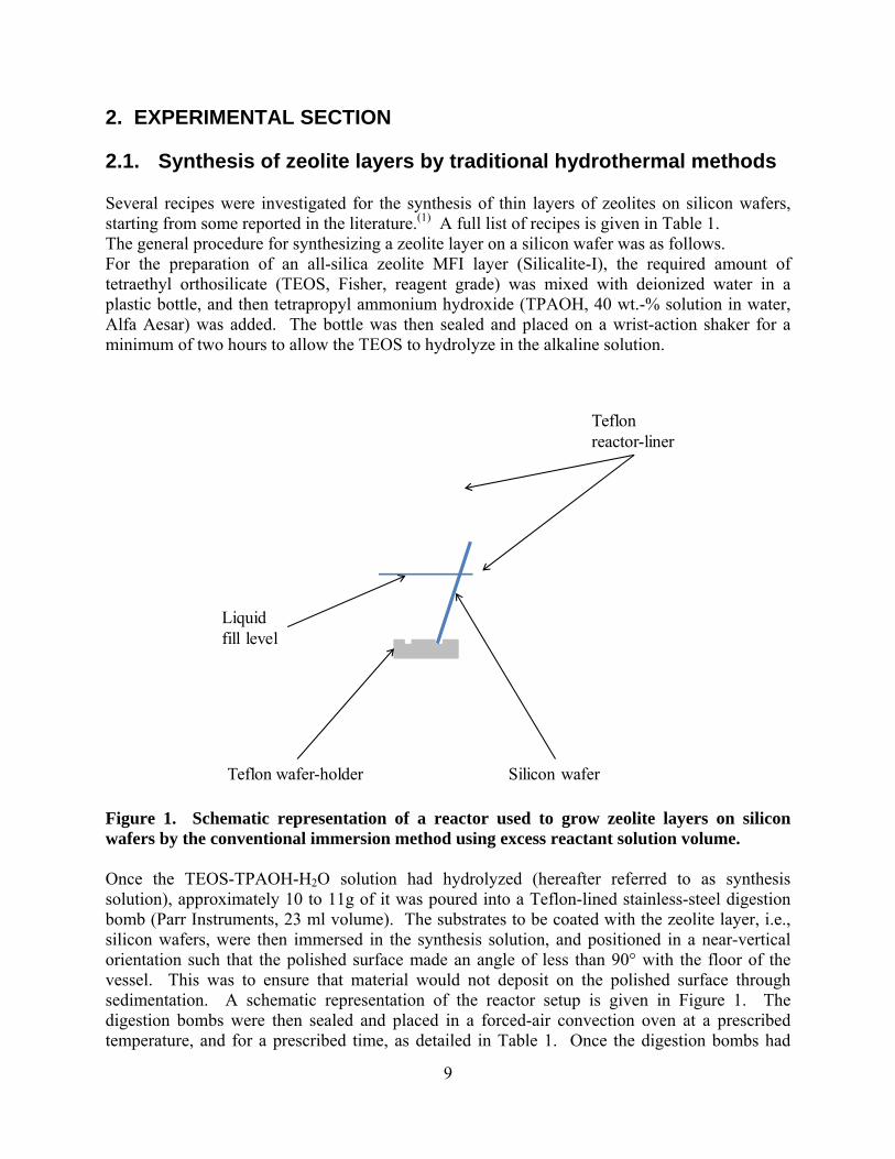
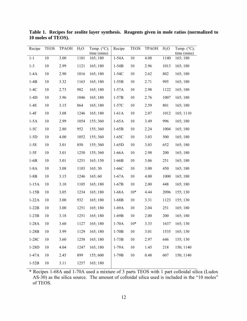
2. EXPERIMENTAL SECTION 2.1. Synthesis of zeolite layers by traditional hydrothermal methods Several recipes were investigated for the synthesis of thin layers of zeolites on silicon wafers, starting from some reported in the literature.(1) A full list of recipes is given in Table 1. The general procedure for synthesizing a zeolite layer on a silicon wafer was as follows. For the preparation of an all-silica zeolite MFI layer (Silicalite-I), the required amount of tetraethyl orthosilicate (TEOS, Fisher, reagent grade) was mixed with deionized water in a plastic bottle, and then tetrapropyl ammonium hydroxide (TPAOH, 40 wt.-% solution in water, Alfa Aesar) was added. The bottle was then sealed and placed on a wrist-action shaker for a minimum of two hours to allow the TEOS to hydrolyze in the alkaline solution.
Figure 1. Schematic representation of a reactor used to grow zeolite layers on silicon wafers by the conventional immersion method using excess reactant solution volume. Once the TEOS-TPAOH-H2O solution had hydrolyzed (hereafter referred to as synthesis solution), approximately 10 to 11g of it was poured into a Teflon-lined stainless-steel digestion bomb (Parr Instruments, 23 ml volume). The substrates to be coated with the zeolite layer, i.e., silicon wafers, were then immersed in the synthesis solution, and positioned in a near-vertical orientation such that the polished surface made an angle of less than 90° with the floor of the vessel. This was to ensure that material would not deposit on the polished surface through sedimentation. A schematic representation of the reactor setup is given in Figure 1. The digestion bombs were then sealed and placed in a forced-air convection oven at a prescribed temperature, and for a prescribed time, as detailed in Table 1. Once the digestion bombs had
Teflon wafer-holder Silicon wafer
Liquidfill level
Teflon reactor-liner
10
cooled to room temperature, they were opened and the wafers were removed using tweezers, rinsed with deionized water, and allowed to dry in ambient air. In some cases, the powder product which formed in solution and sedimented to the floor of the vessel was also harvested by filtration, washing with deionized water, and drying in air at 80 °C. The silicon wafers were approximately 20 mm x 10 mm x 0.5 mm, and were cleaned prior to zeolite layer growth according to several different protocols, as outlined in Table 2. 2.2. Synthesis of zeolite layers by novel methods Two non-traditional approaches were attempted for the controlled growth of thin layers of zeolite on silicon wafers. Details of these experiments are given below. 2.2.1. Volume-minimization The silicon wafers were oriented horizontally in the Teflon-lined stainless-steel digestion bombs, with their polished surfaces facing up, and varying quantities of synthesis solution were poured on top of the wafers. The wafers were either positioned on the floor of the Teflon liner, submerged in synthesis solution, or on coarse-mesh stainless steel gauze which sat on top of a Teflon cup containing a small volume of liquid, as depicted in Figure 2. In the latter case, small quantities of synthesis solution were placed on the surface of the wafer by pipette, taking care to avoid overflow. The digestion bombs were then sealed and placed in a forced-air convection oven at a prescribed temperature, and for a prescribed time. Wafers were harvested, washed, and dried as described in Section 2.1. 2.2.2. Layer growth by partial conversion of silicon wafer Since the principal component of the zeolite structure is silicon (as (SiO4)
4- units), a novel way to prepare a zeolite layer on silicon is via partial conversion of the silicon wafer into zeolite. Silicon wafers for these experiments were thermally oxidized in static air for various periods of time at 1100 °C in order to develop a coating of SiO2 on top of the Si; the conditions and calculated oxide thicknesses(4) from these treatments are given in Table 3. The wafers were then exposed to TPAOH and H2O in Teflon-lined stainless-steel digestion bombs. In some experiments, the wafers were laid horizontally on a platform, polished side up, TPAOH and H2O were deposited on the surface of the wafer by pipette, and deionized water was added to the liner at a level below that of the wafer (e.g., Figure 2). In others, the wafers were immersed in a solution of TPAOH, and positioned in a near-vertical orientation such that the polished surface made an angle of less than 90° with the floor of the vessel, as in Figure 1. The digestion bombs were then sealed and placed in a forced-air convection oven at a prescribed temperature, and for a prescribed time, as detailed in Table 4. Wafers and powders were harvested, washed, and dried as described in Section 2.1.
11
Figure 2. Schematic representation of a reactor used to grow zeolite layers on silicon wafers using reduced reactant solution volume, and with the wafer oriented horizontally above a liquid layer. 2.3. Characterization of zeolite layers X-ray diffraction measurements were performed on a PANalytical X’Pert Pro diffractometer equipped with an X’Celerator multi-position detector, and using Cu Kα radiation. Zeolite-coated silicon wafers were mounted on modeling clay in an aluminum holder, and their heights were adjusted to the appropriate position for diffraction. A Zeiss Supra 55VP field emission gun scanning electron microscope was used to image the samples. Zeolite-coated silicon wafers were attached to the microscope stage using carbon tape, and they were imaged without application of a conductive coating. Images were acquired at 5kV using the secondary electron detector.
Teflon cup
Silicon waferLiquidfill level
Teflon reactor-liner
Steel gauze
12
Table 1. Recipes for zeolite layer synthesis. Reagents given in mole ratios (normalized to 10 moles of TEOS). Recipe TEOS TPAOH H2O Temp. (°C);
* Recipes 1-68A and 1-70A used a mixture of 3 parts TEOS with 1 part colloidal silica (Ludox AS-30) as the silica source. The amount of colloidal silica used is included in the “10 moles” of TEOS.
13
Table 2. Silicon wafer cleaning protocols
Method Solution composition Drying
A 1) Acetone; 15 mins sonication
2) Toluene; 15 mins sonication Ambient air
B 1) 70 vol.% H2SO4 + 30 vol.% H2O2; 30 mins at 90 °C
2) H2O rinse Ambient air
C 1) 10 vol.% HF; 0.5 mins, 25 °C
2) H2O rinse Ambient air
D
1) Xylene reflux; 30 mins
2) 5-part H2O + 1-part H2O2 + 1-part NH4OH; 15 mins at 80 °C
3) 6-part H2O + 1-part H2O2 + 1-part HCl; 15 mins at 80 °C
4) H2O; 10 mins sonication
Wafers transferred into loaded reactors immediately after cleaning, still wet
Method Oxidation time @ 1100 C / hrs Estimated oxide thickness / nm
- 0 25
A 5 280
B 20 620
C 60 1122
14
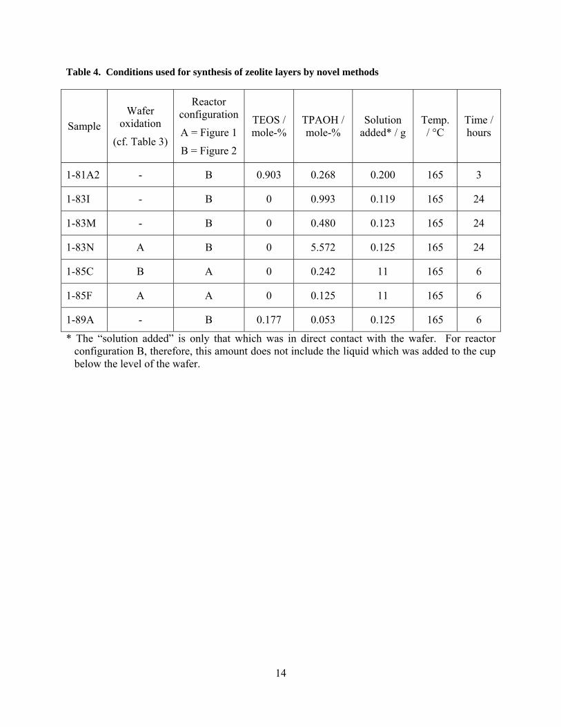
Table 4. Conditions used for synthesis of zeolite layers by novel methods
Sample
Wafer oxidation
(cf. Table 3)
Reactor configuration
A = Figure 1
B = Figure 2
TEOS / mole-%
TPAOH / mole-%
Solution added* / g
Temp. / °C
Time / hours
1-81A2 - B 0.903 0.268 0.200 165 3
1-83I - B 0 0.993 0.119 165 24
1-83M - B 0 0.480 0.123 165 24
1-83N A B 0 5.572 0.125 165 24
1-85C B A 0 0.242 11 165 6
1-85F A A 0 0.125 11 165 6
1-89A - B 0.177 0.053 0.125 165 6
* The “solution added” is only that which was in direct contact with the wafer. For reactor configuration B, therefore, this amount does not include the liquid which was added to the cup below the level of the wafer.
15
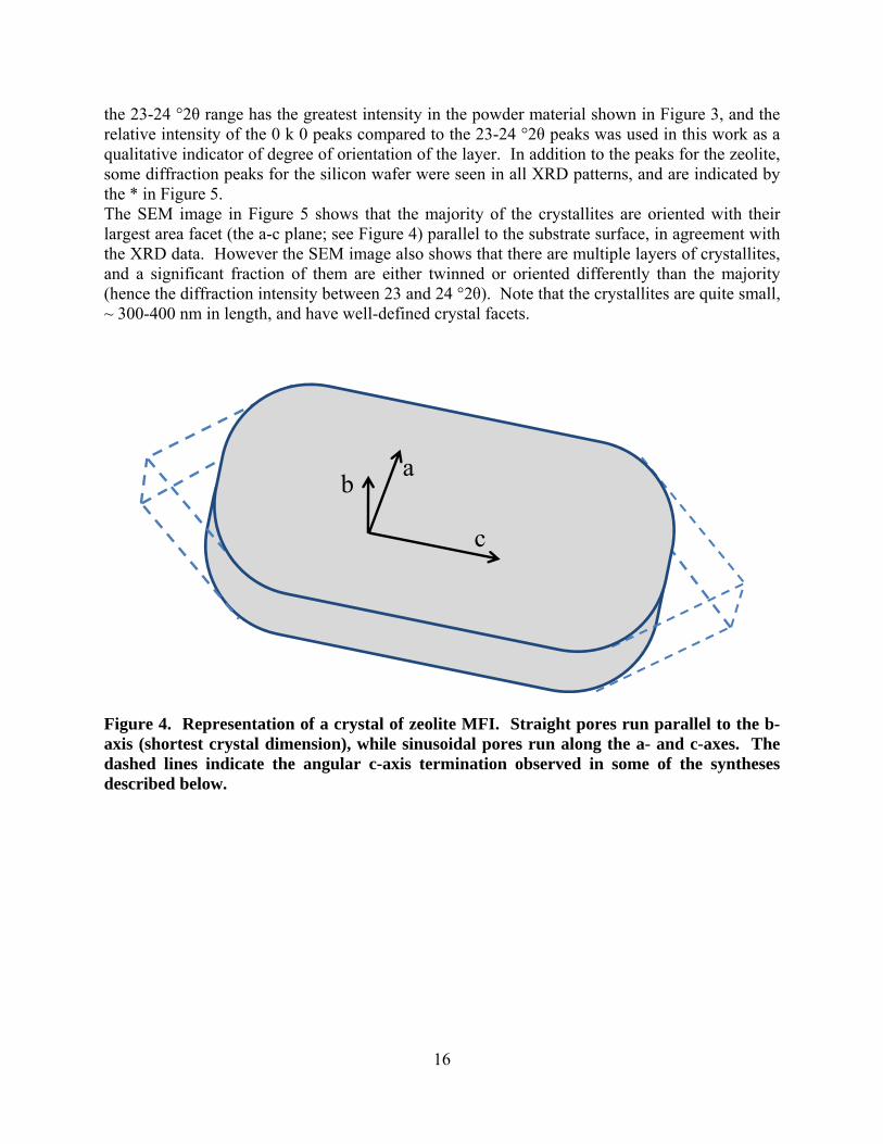
3. RESULTS AND DISCUSSION 3.1. Synthesis of zeolite layers by traditional hydrothermal methods Only a small fraction (a few %) of the zeolite formed during synthesis formed a layer on the silicon wafer; the majority of the zeolite mass formed “homogeneously” in solution and was recovered as a powder on the floor of the vessel after synthesis. Figure 3 shows the XRD pattern of a powder sample harvested after synthesis using recipe 1-3 (Table 1). The XRD pattern compares well with literature examples,(5) and shows that the product is phase-pure all-silica zeolite MFI (also called Silicalite-I).
Figure 3. Typical XRD pattern of a powder sample collected from a Teflon-lined reactor after growth of zeolite layers on silicon wafers. XRD was the principal characterization technique employed, and provided valuable insight into the orientation of the zeolite crystals in the layers grown on silicon wafers. In some cases, little-to-no orientation effects were seen (i.e., the XRD patterns of a layer looked similar to that of the powder), whereas in most cases some degree of preferred orientation of the crystals relative to the wafer surface was observed as discussed below. Figure 4 shows a representation of a crystal of zeolite MFI with the morphology that was typically observed in this work; the crystal axes are indicated, and are referred to below when discussing orientation. Scanning electron microscopy (SEM) was carried out to investigate the topology of selected zeolite layers, and the morphology of the crystals comprising the layers. Synthesis using recipe 1-66C (Table 1) with a wafer cleaned using method A (Table 2) resulted in a layer with preferential crystal orientation such that the straight pores of the zeolite, parallel to the crystal’s b-axis, lay perpendicular to the substrate surface. This preferred orientation is illustrated by the XRD pattern in Figure 5. Apart from a relatively minor intensity for multiple lattice orientations between 23 and 24 °2θ, only 0 k 0 diffraction peaks were observed. Note that
0
1000
2000
3000
4000
5000
6000
7000
8000
9000
5 10 15 20 25 30 35 40 45 50 55 60 65
Inte
nsit
y / c
ps
Degrees 2-theta
1-3C
16
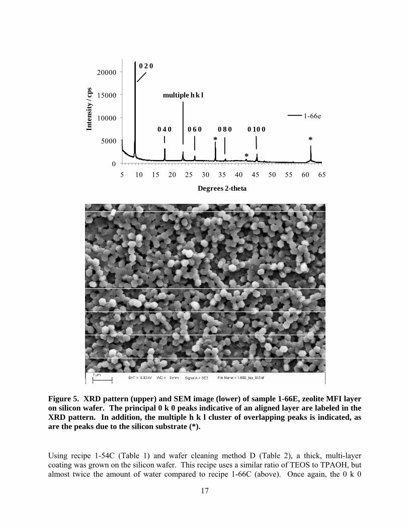
the 23-24 °2θ range has the greatest intensity in the powder material shown in Figure 3, and the relative intensity of the 0 k 0 peaks compared to the 23-24 °2θ peaks was used in this work as a qualitative indicator of degree of orientation of the layer. In addition to the peaks for the zeolite, some diffraction peaks for the silicon wafer were seen in all XRD patterns, and are indicated by the * in Figure 5. The SEM image in Figure 5 shows that the majority of the crystallites are oriented with their largest area facet (the a-c plane; see Figure 4) parallel to the substrate surface, in agreement with the XRD data. However the SEM image also shows that there are multiple layers of crystallites, and a significant fraction of them are either twinned or oriented differently than the majority (hence the diffraction intensity between 23 and 24 °2θ). Note that the crystallites are quite small, ~ 300-400 nm in length, and have well-defined crystal facets.
Figure 4. Representation of a crystal of zeolite MFI. Straight pores run parallel to the b-axis (shortest crystal dimension), while sinusoidal pores run along the a- and c-axes. The dashed lines indicate the angular c-axis termination observed in some of the syntheses described below.
ab
c
17
Figure 5. XRD pattern (upper) and SEM image (lower) of sample 1-66E, zeolite MFI layer on silicon wafer. The principal 0 k 0 peaks indicative of an aligned layer are labeled in the XRD pattern. In addition, the multiple h k l cluster of overlapping peaks is indicated, as are the peaks due to the silicon substrate (*). Using recipe 1-54C (Table 1) and wafer cleaning method D (Table 2), a thick, multi-layer coating was grown on the silicon wafer. This recipe uses a similar ratio of TEOS to TPAOH, but almost twice the amount of water compared to recipe 1-66C (above). Once again, the 0 k 0
0
5000
10000
15000
20000
5 10 15 20 25 30 35 40 45 50 55 60 65
Inte
nsit
y / c
ps
Degrees 2-theta
1-66e
0 2 0
0 4 0 0 6 0 0 8 0 0 10 0
multiple h k l
* *
*
18
peaks dominated the XRD pattern (Figure 6), but a small 2 0 0 peak was also observed at ~ 8 °2θ, in addition to the multiple h k l signature at 23-24 °2θ. The peaks from the silicon wafer were less intense in this sample, due to the relative thickness of the zeolite coating. In this sample the crystallites were an order of magnitude larger than those in Figure 5, and their morphology was slightly different: the c-axis termination was rounded instead of angular.
Figure 6. XRD pattern (upper) and SEM image (lower) of sample 1-57E, zeolite MFI layer on silicon wafer. For XRD peak assignments, refer to Figure 5.
0
10000
20000
30000
40000
50000
60000
70000
80000
90000
100000
5 10 15 20 25 30 35 40 45 50 55 60 65
Inte
nsit
y / c
ps
Degrees 2-theta
1-57E
19
Figure 7. XRD pattern (upper) and SEM image (lower) of sample 1-6-2, zeolite MFI layer on silicon wafer. For XRD peak assignments, refer to Figure 5. A more uniform zeolite layer was obtained when using recipe 1-6B from Table 1 with a wafer cleaned using method A (Table 2); this recipe is even further diluted compared to the two previously-discussed samples. The XRD pattern showed strong 0 k 0 peaks, while the multiple h k l signature at 23-24 °2θ was almost absent; see Figure 7. The peaks from the silicon wafer were somewhat intense in this sample, due to some inter-crystalline gaps in the layer as seen in the SEM image. In some other areas of the wafer, however, SEM revealed a thicker coating with multiple layers of crystallites, as seen in earlier samples (not shown). In this sample the crystallites were approximately 2 – 2.5 µm in length, and the c-axis termination was rounded
0
5000
10000
15000
20000
25000
30000
5 10 15 20 25 30 35 40 45 50 55 60 65
Inte
nsit
y / c
ps
Degrees 2-theta
1-6-2
20
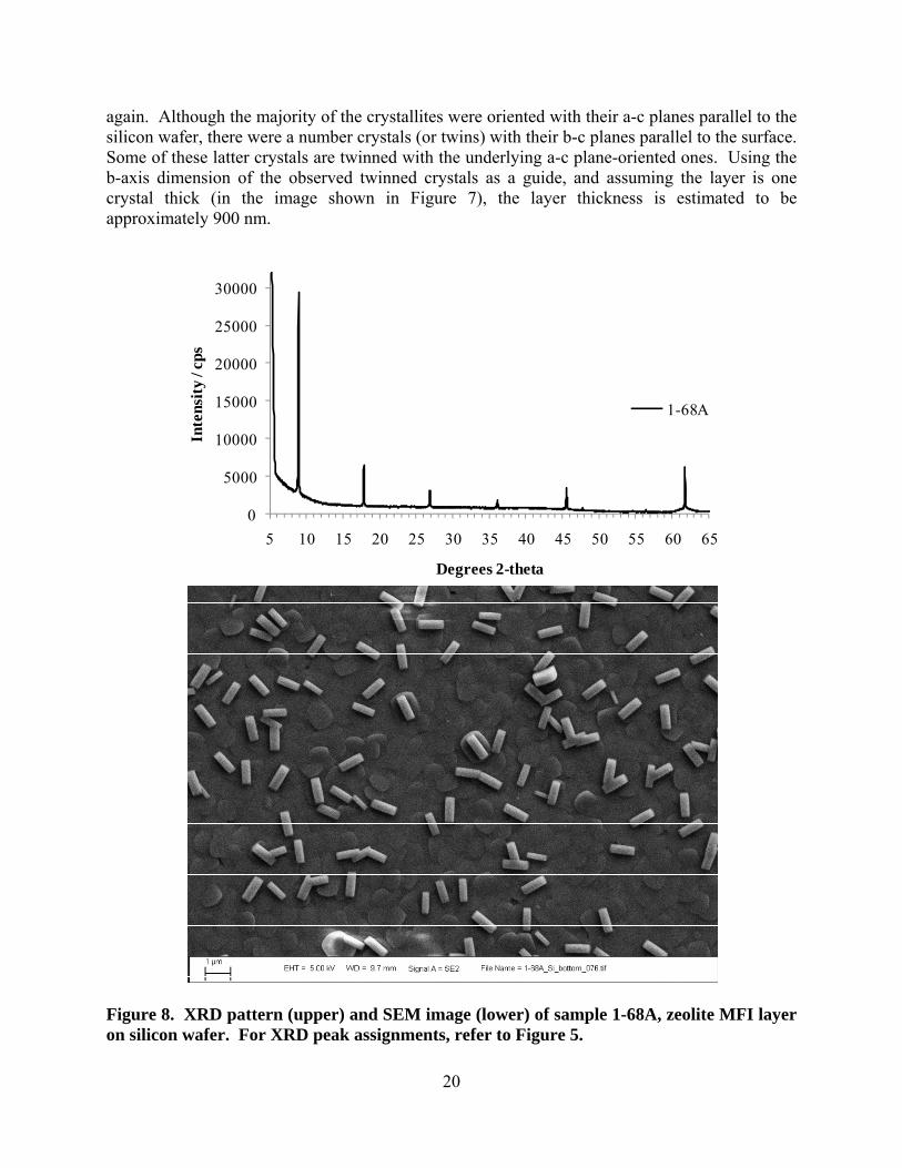
again. Although the majority of the crystallites were oriented with their a-c planes parallel to the silicon wafer, there were a number crystals (or twins) with their b-c planes parallel to the surface. Some of these latter crystals are twinned with the underlying a-c plane-oriented ones. Using the b-axis dimension of the observed twinned crystals as a guide, and assuming the layer is one crystal thick (in the image shown in Figure 7), the layer thickness is estimated to be approximately 900 nm.
Figure 8. XRD pattern (upper) and SEM image (lower) of sample 1-68A, zeolite MFI layer on silicon wafer. For XRD peak assignments, refer to Figure 5.
0
5000
10000
15000
20000
25000
30000
5 10 15 20 25 30 35 40 45 50 55 60 65
Inte
nsit
y / c
ps
Degrees 2-theta
1-68A
21
A similar layer was attained upon increasing the TPAOH concentration slightly (recipe 1-68A in Table 1) as shown in Figure 8, except that the crystallites were approximately 50% of the size of those above. The silicon wafer was cleaned using method E in Table 2 prior to growing the layer. In this particular recipe, approximately ¼ of the TEOS was replaced by a colloidal silica solution, and this probably had an effect on the growth of the zeolite layer. This layer is estimated to be 350 nm thick based on the observed b-c planes of the twinned crystals. Keeping the TPAOH-to-H2O ratio approximately constant while increasing the silica concentration in the synthesis solution by ~ 33% for recipe 1-70A produced a layer that was similar to that shown above. Again, about ¼ of the silica came from the colloidal silica source, and the rest came from TEOS, while the wafer was cleaned before synthesis using method E (Table 2). The XRD pattern showed only 0 k 0 diffraction peaks, while the SEM image shows that the layer consists of tightly-intergrown b-oriented crystallites with only a few degrees of mismatch between the angles of the a-c planes of adjacent crystallites, while some twinning is observed (a-axis sticking up); see Figure 9. This layer is estimated to be about 500 nm thick, as inferred from measuring the observed b-axis lengths of twinned crystals.
22
Figure 9. XRD pattern (upper) and SEM image (lower) of sample 1-70A, zeolite MFI layer on silicon wafer. For XRD peak assignments, refer to Figure 5.
0
20000
40000
60000
80000
100000
120000
5 10 15 20 25 30 35 40 45 50 55 60 65
Inte
nsit
y / c
ps
Degrees 2-theta
1-70A
23
Rationalizing the above observations with the recipes in Table 1, one can conclude that one or more of three factors could result in a better-oriented zeolite layer. One factor is solution concentration, another is silica : TPAOH molar ratio, and the third is substitution of a portion of the TEOS with colloidal silica. In the earlier samples (Figure 5 - Figure 7), the solution concentration and silica : TPAOH ratio were relatively high, while the “better” layers in Figure 8 and Figure 9 were produced from solutions of lower concentration, and lower silica : TPAOH ratio. In order to understand whether one of these two factors is more influential on layer orientation than the other, layers were prepared using solutions of either high concentration and low silica : TPAOH ratio (recipe 1-67A and wafer-cleaning method A, Figure 10), or intermediate concentration and high silica : TPAOH ratio (recipe 1-70B and wafer-cleaning method E, Figure 11). Neither of these recipes used substitution of colloidal silica for TEOS. Synthesis using a high solution concentration and low silica : TPAOH ratio produced a layer with many twinned crystals and relatively poor orientation (Figure 10; note the multiple h k l cluster at ~ 23 °2θ in the XRD pattern). The solution with higher silica : TPAOH ratio and intermediate concentration produced a better oriented layer (no multiple h k l peak in the XRD pattern in Figure 11), although crystal twinning was still evident, and the start of a second layer of crystals was apparent in certain regions of the wafer. To address the effect of substituting colloidal silica for a portion of the TEOS in a synthesis solution, a systematic study was carried out where the TEOS : colloidal silica mole ratio was set at 3:1, 1:1, 1:3, and 0:4, keeping the TPAOH concentration constant. It was found that a zeolite layer was only obtained at the lowest colloidal silica content of those investigated. At 1:1 TEOS : colloidal silica, layer growth was suppressed completely, while at higher colloidal silica contents, amorphous material coated the wafers after synthesis. Hydrothermal treatment was at 165 °C for 130 minutes in each case. From this crude comparison, it appears that the solution concentration is the more dominant factor in determining layer orientation; a lower concentration leads to a better-oriented layer. Substituting colloidal silica for a fraction of the TEOS may be beneficial at low substitution levels, but this effect needs to be investigated in more detail.
24
Figure 10. XRD pattern (upper) and SEM image (lower) of sample 1-67A, zeolite MFI layer on silicon wafer. For XRD peak assignments, refer to Figure 5.
0
10000
20000
30000
40000
50000
5 10 15 20 25 30 35 40 45 50 55 60 65
Inte
nsit
y / c
ps
Degrees 2-theta
1-67A
25
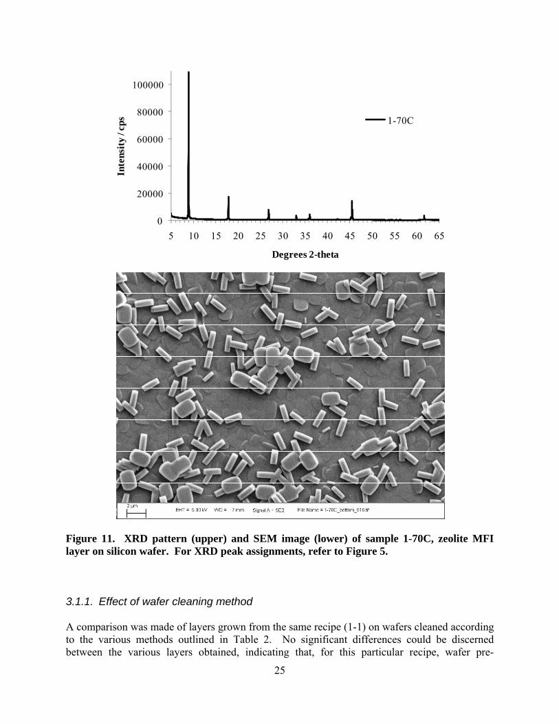
Figure 11. XRD pattern (upper) and SEM image (lower) of sample 1-70C, zeolite MFI layer on silicon wafer. For XRD peak assignments, refer to Figure 5. 3.1.1. Effect of wafer cleaning method A comparison was made of layers grown from the same recipe (1-1) on wafers cleaned according to the various methods outlined in Table 2. No significant differences could be discerned between the various layers obtained, indicating that, for this particular recipe, wafer pre-
0
20000
40000
60000
80000
100000
5 10 15 20 25 30 35 40 45 50 55 60 65
Inte
nsit
y / c
ps
Degrees 2-theta
1-70C
26
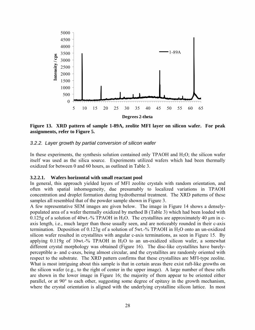
treatment was not critical, and/or that the wafers were stored and handled such that they remained in a clean state, and thus the various cleaning methods had little effect on the wafer surface. 3.2. Synthesis of zeolite layers by novel methods A summary of the solution compositions and synthesis conditions used in these novel approaches to growing zeolite layers on silicon wafers is given in Table 4. 3.2.1. Volume-minimization Initial experiments involved recipe 1-1 (Table 1) with the silicon wafer positioned horizontally on the floor of the reactor, and various quantities of solution were added (2.5 – 5.0g). The layers produced appeared similar to that shown in Figure 6. Subsequent experiments were aimed at reducing the layer thickness by reducing the available nutrients for growth even further. To achieve this, the wafers were supported in a horizontal orientation above the liquid layer in the reactor, polished surface upwards, and small quantities of synthesis solution (approximately 0.15 – 0.20g of recipe 1-1) were placed on top of the wafers by pipette (see Figure 2). The liquid in the bottom of the reactor was either water, or more of the synthesis solution, and served principally as a humidity regulator to reduce evaporation of the liquid from surface of the silicon wafer during hydrothermal treatment. In some cases where the amount of solution added to the wafer was small, layers were obtained by this method which showed XRD patterns similar to a powder (i.e., similar to Figure 3) with randomly-oriented crystallites. In other cases, where the amount of solution added to the wafer surface was larger, preferred crystal orientation was noticed, however the orientation was different from that obtained using the traditional hydrothermal synthesis method (Section 3.1). The XRD pattern in Figure 12 (sample 1-81A2) is an example of such a layer, while the SEM image shows a relatively thick, featureless layer as well as the underlying silicon wafer which shows some evidence of etching. Crystal facets could not be observed in the SEM images of this sample, suggesting that the growth mechanism was significantly different than that observed earlier. It is also possible that the thick layer seen in the SEM image is only partially comprised of zeolite crystallites, with an amorphous material binding it together into a layer. This may be the reason for the relatively high background in the XRD pattern. Due to the low intensity and broadness of the XRD peaks, definitive assignment to specific h k l’s is not possible for the majority of peaks, however the first few diffraction peaks (at the low angle end) are likely from the 2 0 1 (at 11 °2θ), 1 0 3 (at 20 °2θ), and 5 0 1 (at 23 °2θ) planes of the MFI lattice. This would imply that the c-axes of the crystallites were approximately perpendicular to the surface of the substrate; however, further characterization is necessary to confirm this supposition. Additional investigation into the volume minimization approach, this time with serial dilutions of recipe 1-1, showed a transition from random orientation (undiluted recipe 1-1) to highly oriented with the b-axis perpendicular to the silicon wafer support (recipe 1-1 diluted 5-fold with water). The XRD pattern in Figure 13 shows the high degree of crystal orientation achieved in sample 1-89A; only 0 k 0 diffraction peaks were seen, and the multiple h k l cluster around 23 °2θ was absent. SEM images have not yet been recorded for this sample.
27
Figure 12. XRD pattern (upper) and SEM image (lower) of sample 1-81A2, zeolite MFI layer on silicon wafer.
0
200
400
600
800
1000
1200
1400
1600
1800
2000
5 10 15 20 25 30 35 40 45 50 55 60 65
Inte
nsit
y / c
ps
Degrees 2-theta
1-81A2
28
Figure 13. XRD pattern of sample 1-89A, zeolite MFI layer on silicon wafer. For peak assignments, refer to Figure 5. 3.2.2. Layer growth by partial conversion of silicon wafer In these experiments, the synthesis solution contained only TPAOH and H2O; the silicon wafer itself was used as the silica source. Experiments utilized wafers which had been thermally oxidized for between 0 and 60 hours, as outlined in Table 3. 3.2.2.1. Wafers horizontal with small reactant pool In general, this approach yielded layers of MFI zeolite crystals with random orientation, and often with spatial inhomogeneity, due presumably to localized variations in TPAOH concentration and droplet formation during hydrothermal treatment. The XRD patterns of these samples all resembled that of the powder sample shown in Figure 3. A few representative SEM images are given below. The image in Figure 14 shows a densely-populated area of a wafer thermally oxidized by method B (Table 3) which had been loaded with 0.125g of a solution of 40wt.-% TPAOH in H2O. The crystallites are approximately 40 µm in c-axis length, i.e., much larger than those usually seen, and are noticeably rounded in their c-axis termination. Deposition of 0.123g of a solution of 5wt.-% TPAOH in H2O onto an un-oxidized silicon wafer resulted in crystallites with angular c-axis terminations, as seen in Figure 15. By applying 0.119g of 10wt.-% TPAOH in H2O to an un-oxidized silicon wafer, a somewhat different crystal morphology was obtained (Figure 16). The disc-like crystallites have barely-perceptible a- and c-axes, being almost circular, and the crystallites are randomly oriented with respect to the substrate. The XRD pattern confirms that these crystallites are MFI-type zeolite. What is most intriguing about this sample is that in certain areas there exist raft-like growths on the silicon wafer (e.g., to the right of center in the upper image). A large number of these rafts are shown in the lower image in Figure 16; the majority of them appear to be oriented either parallel, or at 90° to each other, suggesting some degree of epitaxy in the growth mechanism, where the crystal orientation is aligned with the underlying crystalline silicon lattice. In most
0
500
1000
1500
2000
2500
3000
3500
4000
4500
5000
5 10 15 20 25 30 35 40 45 50 55 60 65
Inte
nsit
y / c
ps
Degrees 2-theta
1-89A
29
cases, the outline of the raft resembles that of an MFI crystallite with its b-axis perpendicular to the silicon wafer.
Figure 14. SEM image of sample 1-83N, zeolite MFI layer on a thermally-oxidized silicon wafer.
Figure 15. SEM image of sample 1-83M, zeolite MFI layer on silicon wafer.
30
Figure 16. SEM images of sample 1-83I, zeolite MFI layer on silicon wafer. 3.2.2.2. Wafers immersed in a large reactant pool Somewhat better control over the homogeneity of reactant concentration across the wafer surface was achieved by using a larger reactant pool. For these experiments, a reactor set up similar to that shown in Figure 1 was used. In general, a greater degree of preferred orientation was achieved using the immersion technique than was achieved when depositing reactants directly onto the surface (previous section). For example, the XRD patterns in Figure 17 and Figure 18 show one, and two distinct crystal orientations within the sample, respectively. In Figure 17 the crystallites are mostly oriented with their c-axes approximately perpendicular to the substrate (similar to that seen in Figure 12),
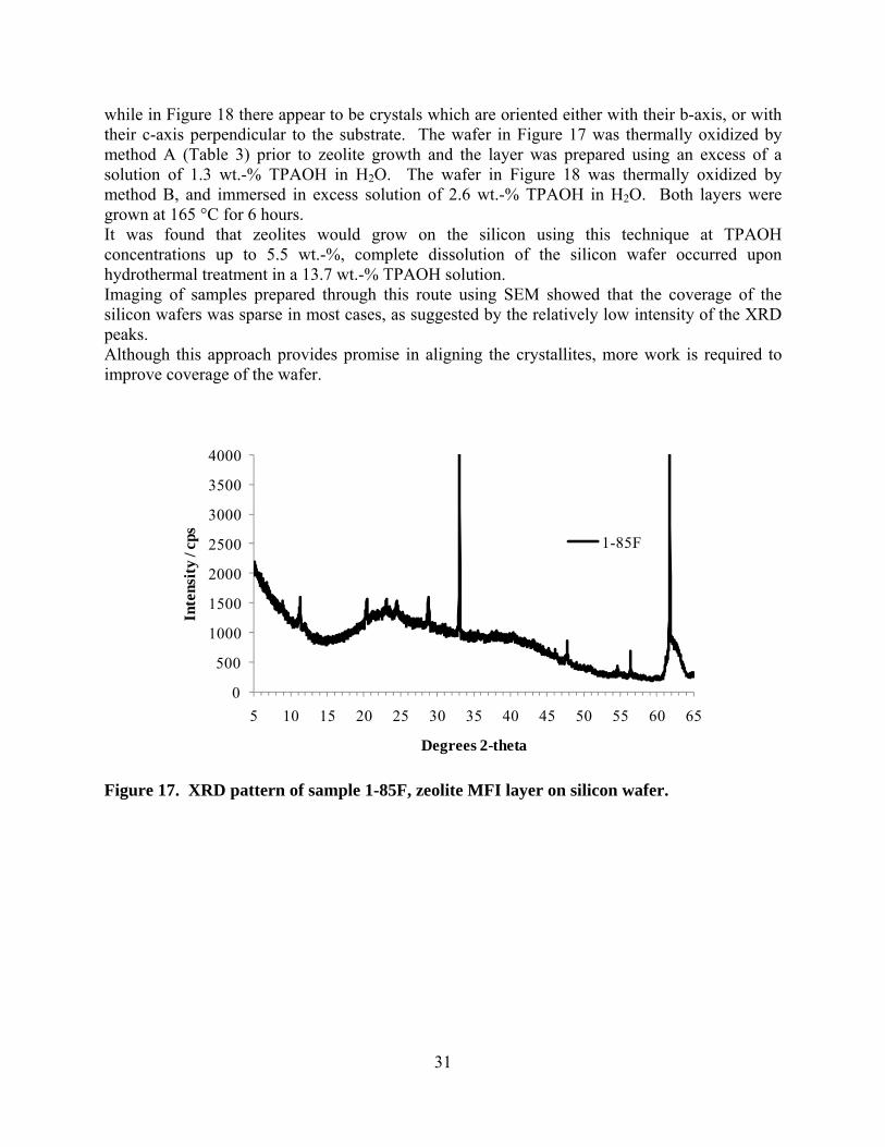
31
while in Figure 18 there appear to be crystals which are oriented either with their b-axis, or with their c-axis perpendicular to the substrate. The wafer in Figure 17 was thermally oxidized by method A (Table 3) prior to zeolite growth and the layer was prepared using an excess of a solution of 1.3 wt.-% TPAOH in H2O. The wafer in Figure 18 was thermally oxidized by method B, and immersed in excess solution of 2.6 wt.-% TPAOH in H2O. Both layers were grown at 165 °C for 6 hours. It was found that zeolites would grow on the silicon using this technique at TPAOH concentrations up to 5.5 wt.-%, complete dissolution of the silicon wafer occurred upon hydrothermal treatment in a 13.7 wt.-% TPAOH solution. Imaging of samples prepared through this route using SEM showed that the coverage of the silicon wafers was sparse in most cases, as suggested by the relatively low intensity of the XRD peaks. Although this approach provides promise in aligning the crystallites, more work is required to improve coverage of the wafer.
Figure 17. XRD pattern of sample 1-85F, zeolite MFI layer on silicon wafer.
0
500
1000
1500
2000
2500
3000
3500
4000
5 10 15 20 25 30 35 40 45 50 55 60 65
Inte
nsit
y / c
ps
Degrees 2-theta
1-85F
32
Figure 18. XRD pattern of sample 1-85C, zeolite MFI layer on silicon wafer. For peak assignments, refer to Figure 5. 4. CONCLUSIONS Conventional hydrothermal synthesis methods enable the growth of highly oriented zeolite crystalline layers on silicon wafers. By modifying synthesis recipes and hydrothermal treatment conditions, layer thickness was reduced to several hundred nanometers while maintaining (and possibly even improving) the degree of orientation of the crystals within the layer such that their straight pores are aligned perpendicular to the silicon wafer surface. While higher solution concentrations favor the formation of smaller crystallites, lower solution concentrations facilitate better overall crystal orientation. Minimization of the synthesis solution volume by placing the solution onto the surface of a horizontal wafer has some potential as a novel method to prepare thin zeolite layers. The dilution of a standard recipe 5-fold produced a very well oriented layer with the straight pores perpendicular to the silicon surface. Partial conversion of the silicon wafer into zeolite also has some potential, although as yet, good control has not been achieved over crystallite orientation. Some orientation effects were seen, but only a relatively low wafer-coverage.
0
1000
2000
3000
4000
5000
6000
5 10 15 20 25 30 35 40 45 50 55 60 65
Inte
nsit
y / c
ps
Degrees 2-theta
1-85C
33
34
5. REFERENCES 1. J.C. Jansen, W. Nugroho, and H. van Bekkum, Proc. 9th Int. Zeolite Conf., Montreal 1992,
pp. 247-54. 2. T.M. Nenoff, S.G. Thoma, C.S. Ashley, and S.T. Reed, US Patent 6,494,326, (2002). 3. M. Choi, K. Na, J. Kim, Y. Sakamoto, O. Terasaki, and R. Ryoo, Nature, 461, 246-9, (2009). 4. See, e.g., http://cleanroom.byu.edu/OxideTimeCalc.phtml 5. See, e.g., M.M.J. Treacy and J.B. Higgins, “Collection of simulated XRD powder patterns for