UM10837 PTN3356 (e)DP to VGA Bridge IC Application Board User’s Manual Rev. 1 — 19 January 2015 User manual Document information Info Content Keywords PTN3356, DisplayPort, eDP, VGA, bridge, application board Abstract This user manual presents the demonstration / application board capability of interfacing an (embedded) DisplayPort source to VGA output. The application board is intended for use as an evaluation and customer demonstration tool, as well as a reference design.
Transcript
UM10837PTN3356 (e)DP to VGA Bridge IC Application Board User’s ManualRev. 1 — 19 January 2015 User manual
Abstract This user manual presents the demonstration / application board capability of interfacing an (embedded) DisplayPort source to VGA output. The application board is intended for use as an evaluation and customer demonstration tool, as well as a reference design.
NXP Semiconductors UM10837PTN3356 (e)DP to VGA Bridge IC Application Board User’s Manual
Contact informationFor more information, please visit: http://www.nxp.com
For sales office addresses, please send an email to: [email protected]
NXP Semiconductors UM10837PTN3356 (e)DP to VGA Bridge IC Application Board User’s Manual
1. Introduction
The PTN3356 is a small package low power DisplayPort to VGA bridge IC optimized primarily for motherboard applications, to convert a DisplayPort signal from the chip set to an analog video signal that directly connects to the VGA connector. The PTN3356 consumes approximately 200 mW of power for video streaming in WUXGA resolution and 410 W of power in low-power mode. The VGA output is powered down when there is no valid DisplayPort source data being transmitted. The PTN3356 is packaged in HVQFN 32 pin, with dimension of 5 mm x 5 mm x 0.85 mm, 0.5 mm pitch.
The PTN3356 is powered from 3.3 V power source, and generated 1.5 V through an internal step-down switch regulator and buck converter for internal core usage and DAC usage.
For cost saving, the external inductor for the buck converter can be removed, the internal LDO can supply 1.5 V for core usage and DAC usage without any re-work. However, using an LDO will consume twice as much power as the buck converter, about 400 mW.
UM10837 provides information including:
• Overall PCB connectors, jumpers, and power supplies
• Equipment/Tools that this board will be interfacing with for board testing
• System level connections such as cables and connectors that this board will be plugged into
This application board is intended to demonstrate the bridging capabilities of the PTN3356 in a low power DP to VGA conversion application.
1.1 Purposes
1.1.1 Engineers
For engineers to evaluate the performance of the PTN3356 and to develop firmware, including collecting and verifying system level features/performances/functionalities such as:
• Verify power management schemes
• Power sequence
• Power consumption measurement during various operating modes
• Allow access to test points and jumpers for measurement and configuration purposes
• Flash over AUX and MS_I2C
• Programming and debug test via MS_I2C
1.1.2 Marketing
For marketing to demonstrate Ultra small DP-VGA features to customers in the field, such as:
• Functional and interoperability test
• This board should be connected to a DP or an eDP source
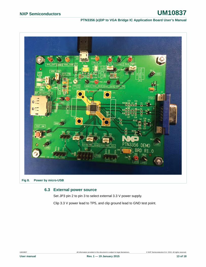
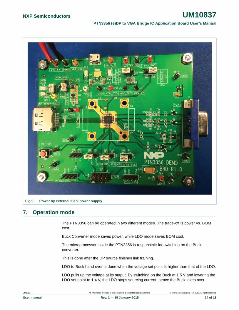
• This board can be powered three ways, as detailed in Section 6 “Power options”
NXP Semiconductors UM10837PTN3356 (e)DP to VGA Bridge IC Application Board User’s Manual
1.1.3 Customers
For customers to evaluate the PTN3356 and to:
• Use I2C to change configuration
2. General description
2.1 Layout of the PTN3356
This application board is designed to evaluate the PTN3356 specifically. An HVQFN32 socket footprint is reserved in preparation for socket installation to test and program ICs.
Due to the bulky socket footprint, the bulk converter design has to be placed on the back side to be close to the PTN3356.
Hence the layout is not optimal as if only the PTN3356 is placed without the socket.
The placement can be dramatically improved in a real application.
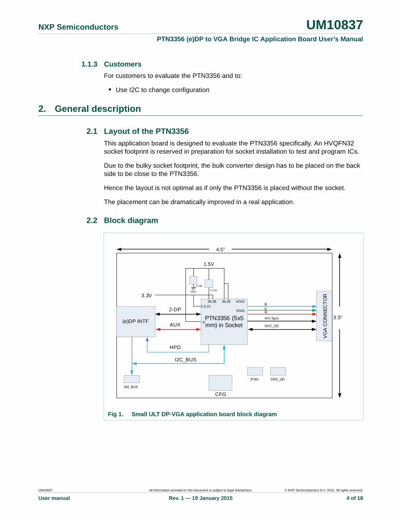
2.2 Block diagram
Fig 1. Small ULT DP-VGA application board block diagram
The microprocessor inside the PTN3356 is responsible for switching on the Buck converter.
This is done after the DP source finishes link training.
LDO to Buck hand over is done when the voltage set point is higher than that of the LDO.
LDO pulls up the voltage at its output. By switching on the Buck at 1.5 V and lowering the LDO set point to 1.4 V, the LDO stops sourcing current, hence the Buck takes over.
NXP Semiconductors UM10837PTN3356 (e)DP to VGA Bridge IC Application Board User’s Manual
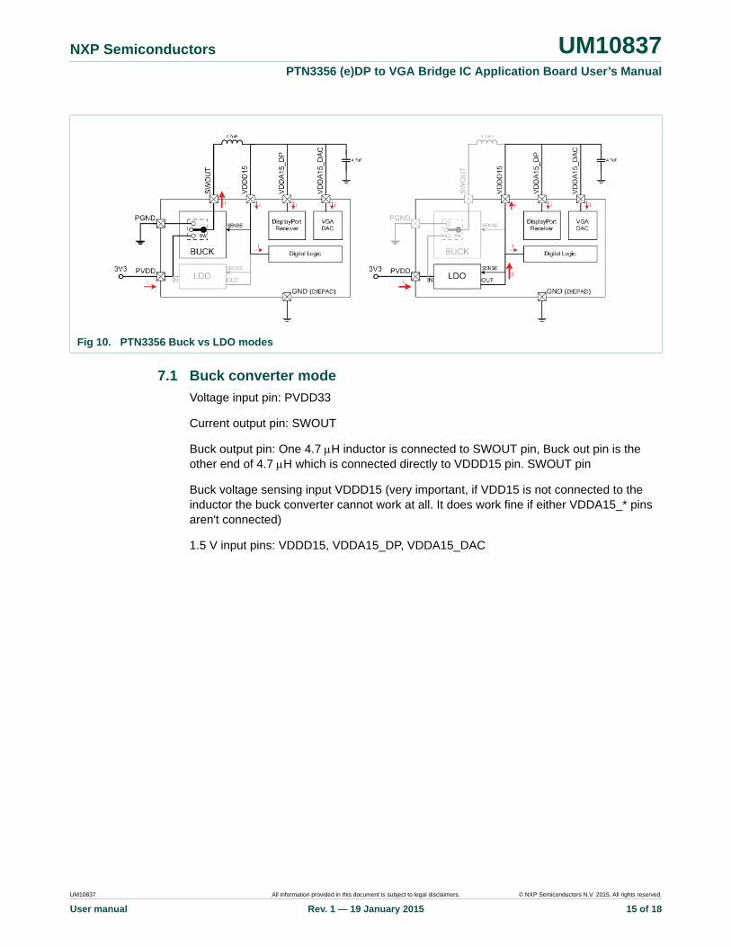
7.1 Buck converter mode
Voltage input pin: PVDD33
Current output pin: SWOUT
Buck output pin: One 4.7 H inductor is connected to SWOUT pin, Buck out pin is the other end of 4.7 H which is connected directly to VDDD15 pin. SWOUT pin
Buck voltage sensing input VDDD15 (very important, if VDD15 is not connected to the inductor the buck converter cannot work at all. It does work fine if either VDDA15_* pins aren't connected)
NXP Semiconductors UM10837PTN3356 (e)DP to VGA Bridge IC Application Board User’s Manual
9. Legal information
9.1 Definitions
Draft — The document is a draft version only. The content is still under internal review and subject to formal approval, which may result in modifications or additions. NXP Semiconductors does not give any representations or warranties as to the accuracy or completeness of information included herein and shall have no liability for the consequences of use of such information.
9.2 Disclaimers
Limited warranty and liability — Information in this document is believed to be accurate and reliable. However, NXP Semiconductors does not give any representations or warranties, expressed or implied, as to the accuracy or completeness of such information and shall have no liability for the consequences of use of such information. NXP Semiconductors takes no responsibility for the content in this document if provided by an information source outside of NXP Semiconductors.
In no event shall NXP Semiconductors be liable for any indirect, incidental, punitive, special or consequential damages (including - without limitation - lost profits, lost savings, business interruption, costs related to the removal or replacement of any products or rework charges) whether or not such damages are based on tort (including negligence), warranty, breach of contract or any other legal theory.
Notwithstanding any damages that customer might incur for any reason whatsoever, NXP Semiconductors’ aggregate and cumulative liability towards customer for the products described herein shall be limited in accordance with the Terms and conditions of commercial sale of NXP Semiconductors.
Right to make changes — NXP Semiconductors reserves the right to make changes to information published in this document, including without limitation specifications and product descriptions, at any time and without notice. This document supersedes and replaces all information supplied prior to the publication hereof.
Suitability for use — NXP Semiconductors products are not designed, authorized or warranted to be suitable for use in life support, life-critical or safety-critical systems or equipment, nor in applications where failure or malfunction of an NXP Semiconductors product can reasonably be expected to result in personal injury, death or severe property or environmental damage. NXP Semiconductors and its suppliers accept no liability for inclusion and/or use of NXP Semiconductors products in such equipment or applications and therefore such inclusion and/or use is at the customer’s own risk.
Applications — Applications that are described herein for any of these products are for illustrative purposes only. NXP Semiconductors makes no representation or warranty that such applications will be suitable for the specified use without further testing or modification.
Customers are responsible for the design and operation of their applications and products using NXP Semiconductors products, and NXP Semiconductors accepts no liability for any assistance with applications or customer product
design. It is customer’s sole responsibility to determine whether the NXP Semiconductors product is suitable and fit for the customer’s applications and products planned, as well as for the planned application and use of customer’s third party customer(s). Customers should provide appropriate design and operating safeguards to minimize the risks associated with their applications and products.
NXP Semiconductors does not accept any liability related to any default, damage, costs or problem which is based on any weakness or default in the customer’s applications or products, or the application or use by customer’s third party customer(s). Customer is responsible for doing all necessary testing for the customer’s applications and products using NXP Semiconductors products in order to avoid a default of the applications and the products or of the application or use by customer’s third party customer(s). NXP does not accept any liability in this respect.
Export control — This document as well as the item(s) described herein may be subject to export control regulations. Export might require a prior authorization from competent authorities.
Evaluation products — This product is provided on an “as is” and “with all faults” basis for evaluation purposes only. NXP Semiconductors, its affiliates and their suppliers expressly disclaim all warranties, whether express, implied or statutory, including but not limited to the implied warranties of non-infringement, merchantability and fitness for a particular purpose. The entire risk as to the quality, or arising out of the use or performance, of this product remains with customer.
In no event shall NXP Semiconductors, its affiliates or their suppliers be liable to customer for any special, indirect, consequential, punitive or incidental damages (including without limitation damages for loss of business, business interruption, loss of use, loss of data or information, and the like) arising out the use of or inability to use the product, whether or not based on tort (including negligence), strict liability, breach of contract, breach of warranty or any other theory, even if advised of the possibility of such damages.
Notwithstanding any damages that customer might incur for any reason whatsoever (including without limitation, all damages referenced above and all direct or general damages), the entire liability of NXP Semiconductors, its affiliates and their suppliers and customer’s exclusive remedy for all of the foregoing shall be limited to actual damages incurred by customer based on reasonable reliance up to the greater of the amount actually paid by customer for the product or five dollars (US$5.00). The foregoing limitations, exclusions and disclaimers shall apply to the maximum extent permitted by applicable law, even if any remedy fails of its essential purpose.
Translations — A non-English (translated) version of a document is for reference only. The English version shall prevail in case of any discrepancy between the translated and English versions.
9.3 TrademarksNotice: All referenced brands, product names, service names and trademarks are the property of their respective owners.