December 2016 DocID026935 Rev 3 1/47 47 UM1818 User manual Street lighting power line modem evaluation board based on ST7580 PLM and STM32 microcontroller Introduction This document explains how to use and set up the firmware and the software designed for the STEVAL-IHP007V1 board and all the necessary setup for using the hardware. The system is based to the ST7580 data link protocol firmware, data link protocol described in the application note AN4018. ST7580 data link protocol firmware is organized in a layer structure. A dedicated layer allows the user to design its own application interfacing to the evaluation board features with very simple and easy to use APIs. Dedicated software graphic user interface (GUI) allows the user to use all the embedded features interfacing the PLM evaluation board with the PC via an RS232 communication port. This firmware is developed using STM32F10x standard peripherals library Rel.3.5.0 and IAR Embedded Workbench ® IDE for STM32 microcontrollers Rel. 6.50x The STEVAL-IHP007V1 hardware evaluation board embeds an ARM 32-bit Cortex™-M3 core-based STM32F103xB and an ST7580 PSK multi mode power line networking system- on-chip. Figure 1. STEVAL-IHP007V1 evaluation board www.st.com
Transcript
December 2016 DocID026935 Rev 3 1/47
47
UM1818User manual
Street lighting power line modem evaluation board based onST7580 PLM and STM32 microcontroller
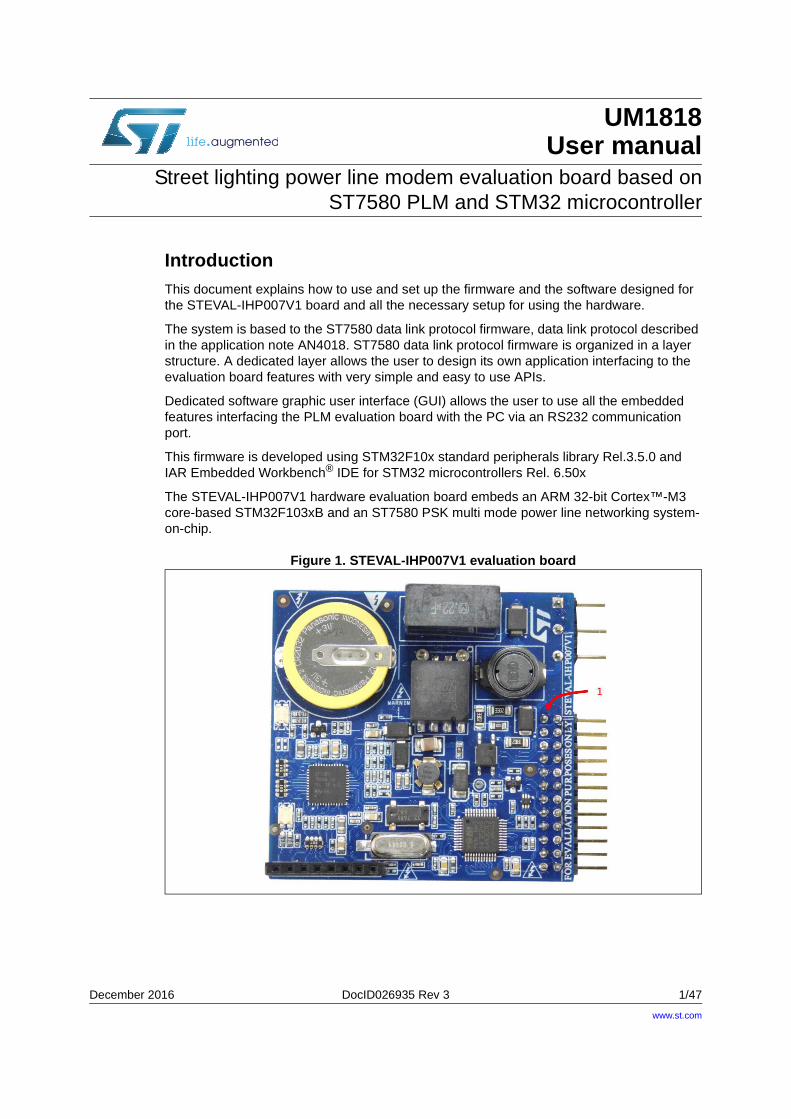
IntroductionThis document explains how to use and set up the firmware and the software designed for the STEVAL-IHP007V1 board and all the necessary setup for using the hardware.
The system is based to the ST7580 data link protocol firmware, data link protocol described in the application note AN4018. ST7580 data link protocol firmware is organized in a layer structure. A dedicated layer allows the user to design its own application interfacing to the evaluation board features with very simple and easy to use APIs.
Dedicated software graphic user interface (GUI) allows the user to use all the embedded features interfacing the PLM evaluation board with the PC via an RS232 communication port.
This firmware is developed using STM32F10x standard peripherals library Rel.3.5.0 and IAR Embedded Workbench® IDE for STM32 microcontrollers Rel. 6.50x
The STEVAL-IHP007V1 hardware evaluation board embeds an ARM 32-bit Cortex™-M3 core-based STM32F103xB and an ST7580 PSK multi mode power line networking system-on-chip.
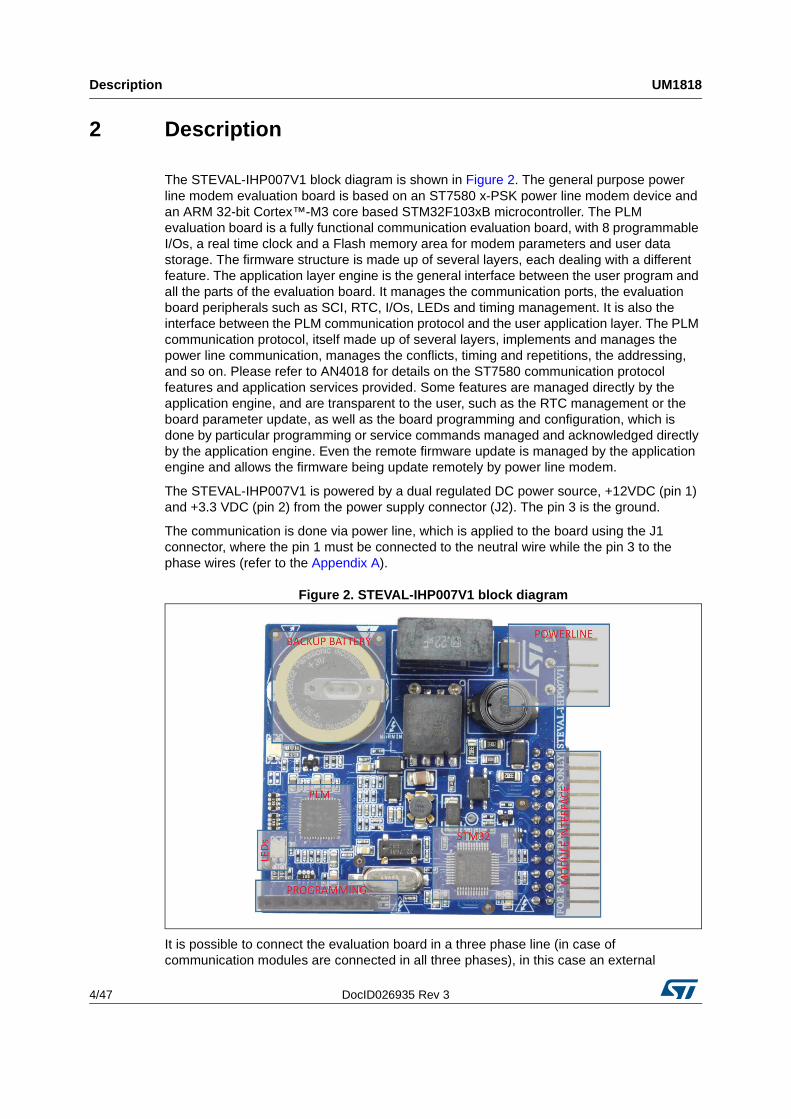
The STEVAL-IHP007V1 block diagram is shown in Figure 2. The general purpose power line modem evaluation board is based on an ST7580 x-PSK power line modem device and an ARM 32-bit Cortex™-M3 core based STM32F103xB microcontroller. The PLM evaluation board is a fully functional communication evaluation board, with 8 programmable I/Os, a real time clock and a Flash memory area for modem parameters and user data storage. The firmware structure is made up of several layers, each dealing with a different feature. The application layer engine is the general interface between the user program and all the parts of the evaluation board. It manages the communication ports, the evaluation board peripherals such as SCI, RTC, I/Os, LEDs and timing management. It is also the interface between the PLM communication protocol and the user application layer. The PLM communication protocol, itself made up of several layers, implements and manages the power line communication, manages the conflicts, timing and repetitions, the addressing, and so on. Please refer to AN4018 for details on the ST7580 communication protocol features and application services provided. Some features are managed directly by the application engine, and are transparent to the user, such as the RTC management or the board parameter update, as well as the board programming and configuration, which is done by particular programming or service commands managed and acknowledged directly by the application engine. Even the remote firmware update is managed by the application engine and allows the firmware being update remotely by power line modem.
The STEVAL-IHP007V1 is powered by a dual regulated DC power source, +12VDC (pin 1) and +3.3 VDC (pin 2) from the power supply connector (J2). The pin 3 is the ground.
The communication is done via power line, which is applied to the board using the J1 connector, where the pin 1 must be connected to the neutral wire while the pin 3 to the phase wires (refer to the Appendix A).
Figure 2. STEVAL-IHP007V1 block diagram
It is possible to connect the evaluation board in a three phase line (in case of communication modules are connected in all three phases), in this case an external
DocID026935 Rev 3 5/47
UM1818 Description
47
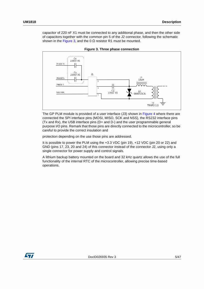
capacitor of 220 nF X1 must be connected to any additional phase, and then the other side of capacitors together with the common pin 5 of the J2 connector, following the schematic shown in the Figure 3, and the 0 Ω resistor R1 must be mounted.
Figure 3. Three phase connection
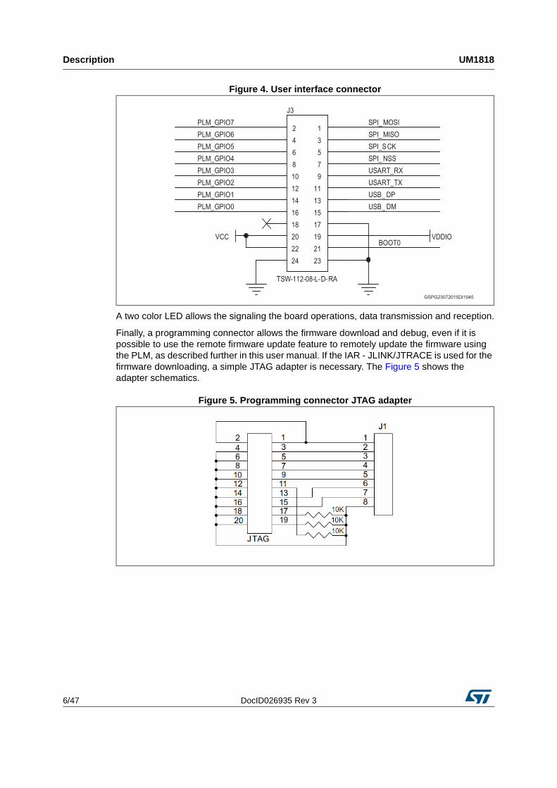
The GP PLM module is provided of a user interface (J3) shown in Figure 4 where there are connected the SPI interface pins (MOSI, MISO, SCK and NSS), the RS232 interface pins (Tx and Rx), the USB interface pins (D+ and D-) and the user programmable general purpose I/O pins. Remark that those pins are directly connected to the microcontroller, so be careful to provide the correct insulation and
protection depending on the use those pins are addressed.
It is possible to power the PLM using the +3.3 VDC (pin 19), +12 VDC (pin 20 or 22) and GND (pins 17, 23, 20 and 24) of this connector instead of the connector J2, using only a single connector for power supply and control signals.
A lithium backup battery mounted on the board and 32 kHz quartz allows the use of the full functionality of the internal RTC of the microcontroller, allowing precise time-based operations.
Description UM1818
6/47 DocID026935 Rev 3
Figure 4. User interface connector
A two color LED allows the signaling the board operations, data transmission and reception.
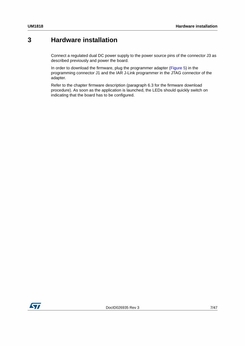
Finally, a programming connector allows the firmware download and debug, even if it is possible to use the remote firmware update feature to remotely update the firmware using the PLM, as described further in this user manual. If the IAR - JLINK/JTRACE is used for the firmware downloading, a simple JTAG adapter is necessary. The Figure 5 shows the adapter schematics.
Figure 5. Programming connector JTAG adapter
PLM_GPIO0
PLM_GPIO1
PLM_GPIO2
PLM_GPIO3
PLM_GPIO4
PLM_GPIO5
PLM_GPIO6
PLM_GPIO7
BOOT0
SPI_ MOSI
SPI_ MISO
SPI_SCK
SPI_ NSS
USB_ DM
USB_ DP
USART_TX
USART_RX
VDDIOVCC
12
34
56
78
910
1112
1314
1516
1718
1920
2122
2324
J3
TSW-112-08-L-D-RA
GSPG23072015DI1045
DocID026935 Rev 3 7/47
UM1818 Hardware installation
47
3 Hardware installation
Connect a regulated dual DC power supply to the power source pins of the connector J3 as described previously and power the board.
In order to download the firmware, plug the programmer adapter (Figure 5) in the programming connector J1 and the IAR J-Link programmer in the JTAG connector of the adapter.
Refer to the chapter firmware description (paragraph 6.3 for the firmware download procedure). As soon as the application is launched, the LEDs should quickly switch on indicating that the board has to be configured.
Firmware description UM1818
8/47 DocID026935 Rev 3
4 Firmware description
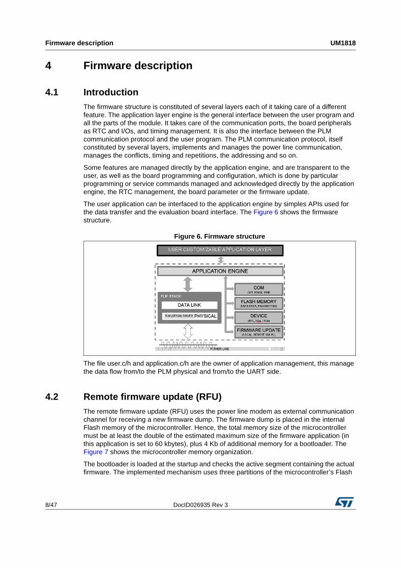
4.1 IntroductionThe firmware structure is constituted of several layers each of it taking care of a different feature. The application layer engine is the general interface between the user program and all the parts of the module. It takes care of the communication ports, the board peripherals as RTC and I/Os, and timing management. It is also the interface between the PLM communication protocol and the user program. The PLM communication protocol, itself constituted by several layers, implements and manages the power line communication, manages the conflicts, timing and repetitions, the addressing and so on.
Some features are managed directly by the application engine, and are transparent to the user, as well as the board programming and configuration, which is done by particular programming or service commands managed and acknowledged directly by the application engine, the RTC management, the board parameter or the firmware update.
The user application can be interfaced to the application engine by simples APIs used for the data transfer and the evaluation board interface. The Figure 6 shows the firmware structure.
Figure 6. Firmware structure
The file user.c/h and application.c/h are the owner of application management, this manage the data flow from/to the PLM physical and from/to the UART side.
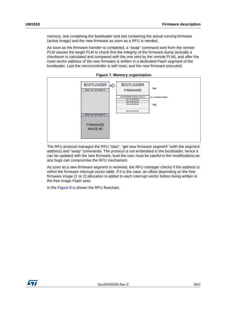
4.2 Remote firmware update (RFU)The remote firmware update (RFU) uses the power line modem as external communication channel for receiving a new firmware dump. The firmware dump is placed in the internal Flash memory of the microcontroller. Hence, the total memory size of the microcontroller must be at least the double of the estimated maximum size of the firmware application (in this application is set to 60 kbytes), plus 4 Kb of additional memory for a bootloader. The Figure 7 shows the microcontroller memory organization.
The bootloader is loaded at the startup and checks the active segment containing the actual firmware. The implemented mechanism uses three partitions of the microcontroller’s Flash
DocID026935 Rev 3 9/47
UM1818 Firmware description
47
memory, one containing the bootloader and two containing the actual running firmware (active image) and the new firmware as soon as a RFU is needed.
As soon as the firmware transfer is completed, a “swap” command sent from the remote PLM causes the target PLM to check first the integrity of the firmware dump (actually a checksum is calculated and compared with the one sent by the remote PLM), and after the reset vector address of the new firmware is written in a dedicated Flash segment of the bootloader. Last the microcontroller is self reset, and the new firmware executed.
Figure 7. Memory organization
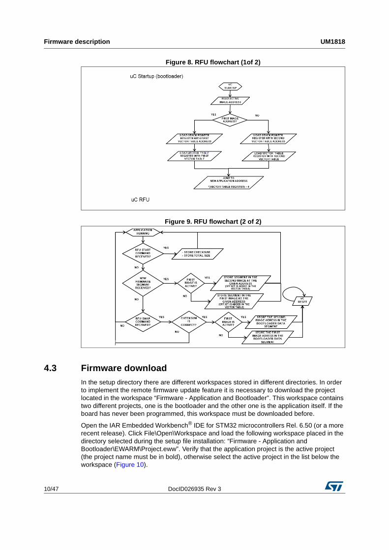
The RFU protocol manages the RFU “start”, “get new firmware segment” (with the segment address) and “swap” commands. The protocol is not embedded in the bootloader, hence it can be updated with the new firmware, bust the user must be careful in the modifications as any bugs can compromise the RFU mechanism.
As soon as a new firmware segment is received, the RFU manager checks if the address is within the firmware interrupt vector table. If it is the case, an offset depending on the free firmware image (1 or 2) allocation is added to each interrupt vector before being written in the free image Flash area.
In the Figure 8 is shown the RFU flowchart.
Firmware description UM1818
10/47 DocID026935 Rev 3
Figure 8. RFU flowchart (1of 2)
Figure 9. RFU flowchart (2 of 2)
4.3 Firmware downloadIn the setup directory there are different workspaces stored in different directories. In order to implement the remote firmware update feature it is necessary to download the project located in the workspace “Firmware - Application and Bootloader”. This workspace contains two different projects, one is the bootloader and the other one is the application itself. If the board has never been programmed, this workspace must be downloaded before.
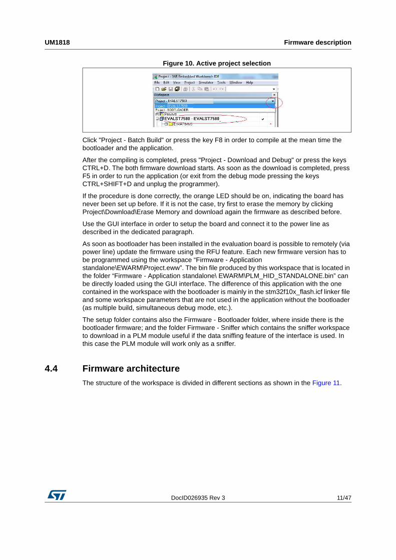
Open the IAR Embedded Workbench® IDE for STM32 microcontrollers Rel. 6.50 (or a more recent release). Click File\Open\Workspace and load the following workspace placed in the directory selected during the setup file installation: “Firmware - Application and Bootloader\EWARM\Project.eww”. Verify that the application project is the active project (the project name must be in bold), otherwise select the active project in the list below the workspace (Figure 10).
DocID026935 Rev 3 11/47
UM1818 Firmware description
47
Figure 10. Active project selection
Click "Project - Batch Build" or press the key F8 in order to compile at the mean time the bootloader and the application.
After the compiling is completed, press "Project - Download and Debug" or press the keys CTRL+D. The both firmware download starts. As soon as the download is completed, press F5 in order to run the application (or exit from the debug mode pressing the keys CTRL+SHIFT+D and unplug the programmer).
If the procedure is done correctly, the orange LED should be on, indicating the board has never been set up before. If it is not the case, try first to erase the memory by clicking Project\Download\Erase Memory and download again the firmware as described before.
Use the GUI interface in order to setup the board and connect it to the power line as described in the dedicated paragraph.
As soon as bootloader has been installed in the evaluation board is possible to remotely (via power line) update the firmware using the RFU feature. Each new firmware version has to be programmed using the workspace “Firmware - Application standalone\EWARM\Project.eww”. The bin file produced by this workspace that is located in the folder “Firmware - Application standalone\ EWARM\PLM_HID_STANDALONE.bin” can be directly loaded using the GUI interface. The difference of this application with the one contained in the workspace with the bootloader is mainly in the stm32f10x_flash.icf linker file and some workspace parameters that are not used in the application without the bootloader (as multiple build, simultaneous debug mode, etc.).
The setup folder contains also the Firmware - Bootloader folder, where inside there is the bootloader firmware; and the folder Firmware - Sniffer which contains the sniffer workspace to download in a PLM module useful if the data sniffing feature of the interface is used. In this case the PLM module will work only as a sniffer.
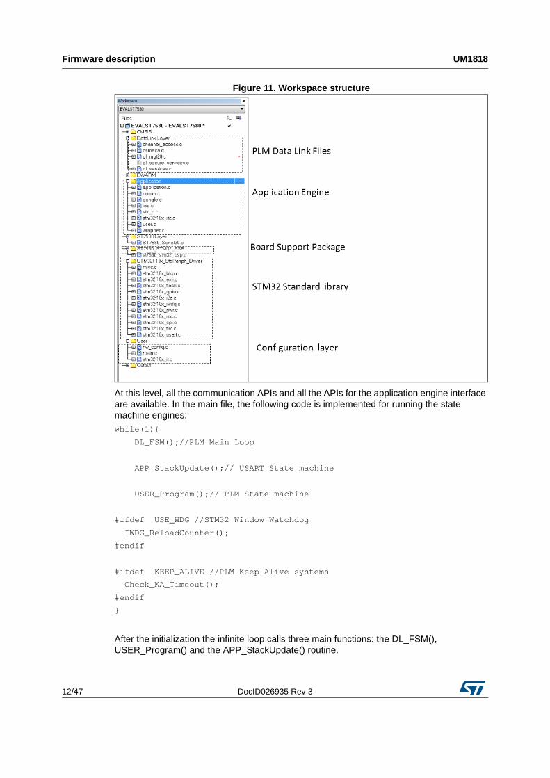
4.4 Firmware architectureThe structure of the workspace is divided in different sections as shown in the Figure 11.
Firmware description UM1818
12/47 DocID026935 Rev 3
Figure 11. Workspace structure
At this level, all the communication APIs and all the APIs for the application engine interface are available. In the main file, the following code is implemented for running the state machine engines:while(1)
DL_FSM();//PLM Main Loop
APP_StackUpdate();// USART State machine
USER_Program();// PLM State machine
#ifdef USE_WDG //STM32 Window Watchdog
IWDG_ReloadCounter();
#endif
#ifdef KEEP_ALIVE //PLM Keep Alive systems
Check_KA_Timeout();
#endif
After the initialization the infinite loop calls three main functions: the DL_FSM(), USER_Program() and the APP_StackUpdate() routine.
DocID026935 Rev 3 13/47
UM1818 Firmware description
47
The DL_FSM() is the PLM stack main loop, this manage the PLM low level communication. The application engine “APP_StackUpdate()” is the state machine which runs inside the PLM application state machine; this uses the data link service provided from DL_Service layer.
The user program implemented in this user manual realizes a bridge between the power line communication and the COM port: all data arriving from the COM port addressed to another PLM module is sent via PLM, and in turn all data received from PLM is sent back to the COM port. It is necessary that the user program does not stop the core operations (looping instructions) without calling the application engine.
All the hardware configurations are contained in the board support package file, and the file DL_SimpleNodeConf contains the data link configuration parameters and the PLM modem configuration value (frequency, modulation zero crossing delay, etc.).
The next paragraph lists all the data types and the APIs used in the application engine that can be modified by the user if different needs arise.
4.5 Firmware data typesThe data type found in the wrapper.h module, are listed hereafter:/* USER FRAME STRUCTURE */
typedef struct
APP_ftype_t type;
bool broadcast;
u8 address[6];
u8 len;
u8 data[USER_PAYLOAD_SIZE]; /* MAX PAY LOAD SIZE: 100 bytes */
bool EnableTX
APP_frame_t;
/* APPLICATION FRAME TYPE */
typedef enum
APP_DATA_FRAME = 0x00,
APP_SERVICE_FRAME = 0x01,
APP_PING_FRAME = 0x02,
APP_ERROR_FRAME = 0x03,
APP_PROGRAMMING_FRAME = 0x04,
APP_ACK_FRAME = 0x05,
APP_MIB_FRAME = 0x06
APP_ftype_t;
Firmware description UM1818
14/47 DocID026935 Rev 3
/* APPLICATION ERRORS */
typedef enum
APP_ERROR_NONE = 0x00, // No err or
APP_ERROR_GENERIC = 0x01, // Generi c communication error
APP_ERROR_WRONG_PROG_GROUP = 0x09, // Wrong programming group error
APP_ERROR_DEVICE_BLANK = 0x0a, // Device blank
APP_ERROR_RTC_ERROR = 0x0b, // Error setting the system time
APP_ERROR_WATCHDOG_DISABLED = 0x0c, // Hardwa re reset impossible
APP_ERROR_NODE_INIT_FAILED = 0x0d, // Node i nitialization failure
APP_ERROR_RTC_DISABLED = 0x0e // Intern al RTC disabled
APP_ERROR_t;
/* PROGRAMMING GROUPS */
typedef enum
PROG_GRP_DEVICE_DATA = 0x00, // Device Data
PROG_GRP_LL_STACK_PARAM = 0x01, // Link layer s tack parameters
PROG_GRP_USER_DATA = 0x02 // User program
APP_PROG_GROUP_t;
/* SERVICE COMMANDS */
typedef enum
/* NATIVE SERVICE COMMANDS */
SERVICE_SOFTWARE_RESET = 0x00,// Reset interna l state machines
SERVICE_HARDWARE_RESET = 0x01,// Module hardwa re reset
SERVICE_PARAM_SET = 0x02,// Set service p arameters
SERVICE_PARAM_GET = 0x03,// Get service p arameters
SERVICE_INPUTS_GET = 0x04,// Get general p urpose inputs pin status
SERVICE_OUTPUTS_SET = 0x05,// Set general p urpose outputs pins value
SERVICE_FW_REL_GET = 0x06,// Get the stack and the module firmware release
SERVICE_PLM_CLOCK_SET = 0x07,// Set the inter nal time clock value
DocID026935 Rev 3 15/47
UM1818 Firmware description
47
SERVICE_PLM_CLOCK_GET = 0x08,// Get the inter nal time clock value
SERVICE_IO_CONFIG_SET = 0x09,// Set the gener al purpose input and output pins
SERVICE_IO_CONFIG_GET = 0x0a,// Get the gener al purpose input and output pins
SERVICE_NET_DISCOVER_REQ = 0x0b,
SERVICE_RFU_SET_IMG_HEADER = 0x0c,
SERVICE_RFU_SET_IMG_DATA = 0x0d,
SERVICE_RFU_SWAP_IMG = 0x0e,
SERVICE_SN_SET = 0x0f,
SERVICE_SN_GET = 0x10
/* USER DEFINED SERVICE COMANDS */
// SERVICE_USER_CMD_xx = 0x.., // User defi ned service commands (0x0b to 0x7f)
APP_SER_CMD_t;
4.6 Firmware frame typesThis paragraph describes all the frame types that are implemented in this firmware. In each field there is also the description.
4.6.1 Communication frames types
Frames exchanged between two PLM modules or between a PLM module and an external device connected to the COMM interface.
From the COMM interface module (USART)
/* BROADCAST_FLAG = 0x80 -> data sent in broadcast - BROADCAST_FLAG = 0x00 -> data sent in unicast */
From / to communication interface (PLM, USART)
buffer[0] = n + 10;
buffer[1] = DATA_FRAME_TYPE | BROADCAST_FLAG;
buffer[2,..7] = target_module.address;
buffer[8,..8+n-1] = user_data[n];
buffer[8+n,8+n+1] = CRC16;
// Data frame payload length (n + 10)
// Data frame type
// Target device address (6 bytes)
// User data (n bytes, at least 1)
// CRC-16
frame.type = DATA_FRAME_TYPE;
frame.len = n;
frame.broadcast = TRUE / FALSE;
frame.address = target_module.address;
frame.data[n] = service_data[n];
// Data frame type
// Data frame payload length
// TRUE = broadcast, FALSE = unicast
// Target device address (6 bytes)
// User data (n bytes)
Firmware description UM1818
16/47 DocID026935 Rev 3
4.6.2 Ping frames
This particular frame is used to ping a remote (via PLM interface) or a local (via COMM interface) module. When the ping frame is received, this is managed directly at the data link layer and is not notified at the application and consequently the user levels.
From the COMM interface module (USART).
From / to communication interface (PLM, USART)
4.6.3 Error frames
Can be considered as data frames; they are user error frames from user application level addressed to a target PLM module.
Frames containing service commands concerning both some native module features (internal clock, general purpose inputs and outputs, etc.) and user defined service frames. Native frames are managed directly by the application engine.
From the COMM interface module (USART)
/* BROADCAST_FLAG = 0x80 -> data sent in broadcast - BROADCAST_FLAG = 0x00 -> data sent in unicast */
From / to communication interface (PLM, USART)
buffer[0] = n + 11;
buffer[1] = APP_SERVICE_FRAME | BROADCAST_FLAG;
buffer[2,..7] = target_module.address;
buffer[8] = ( APP_SER_CMD_t)command;
buffer[9,..9+n-1] = service_data[n];
buffer[9+n, 9+n+1] = CRC16;
// Service frame payload length (n + 11)
// Service frame type
// Target device address (6 bytes)
// Service command
// Service data
// CRC-16
buffer[0] = n + 11;
buffer[1] = DATA_FRAME_TYPE;
buffer[2,..7] = target_module.address;
buffer[8] = (APP_SER_CMD_t)command/APP_ACK_FRAME;
buffer[9,..n] = service_data[n]/Command_Echo;
buffer[n+1,n+2] = CRC16;
// length
// Service or ACK frame type
// Target device address (6 bytes)
// Service command/ACK
// Service data or Command echo(n=1)
Firmware description UM1818
18/47 DocID026935 Rev 3
Service command list
PLM reset: software, hardware
From the COMM interface (USART)
Note: Any response from PLM module
/* NATIVE SERVICE COMMANDS */
SERVICE_SOFTWARE_RESET = 0x00,
SERVICE_HARDWARE_RESET = 0x01,
SERVICE_PARAM_SET = 0x02,
SERVICE_PARAM_GET = 0x03,
SERVICE_INPUTS_GET = 0x04,
SERVICE_OUTPUTS_SET = 0x05,
SERVICE_FW_REL_GET = 0x06,
SERVICE_PLM_CLOCK_SET = 0x07,
SERVICE_PLM_CLOCK_GET = 0x08,
SERVICE_IO_CONFIG_SET = 0x09,
SERVICE_IO_CONFIG_GET = 0x0a,
SERVICE_NET_DISCOVER_REQ = 0x0b,
SERVICE_RFU_SET_IMG_HEADER = 0x0c,
SERVICE_RFU_SET_IMG_DATA = 0x0d,
SERVICE_RFU_SWAP_IMG = 0x0e,
SERVICE_SN_SET = 0x0f,
SERVICE_SN_GET = 0x10
/* USER DEFINED SERVICE COMANDS */
0x.. = SERVICE_USER_CMD_xx
// Reset internal state machines
// Module hardware reset
// Set service parameters
// Get service parameters
// Get general purpose inputs pin status
// Set general purpose outputs pins value
// Get the stack and the module firmware release
// Set the internal time clock value
// Get the internal time clock value
// Set the general purpose input and output pins
// Get the general purpose input and output pins
buffer[0] = 11;
buffer[1] = APP_SERVICE_FRAME;
buffer[2,..7] = target_module.address;
/* FOR SOFTWARE RESET */
buffer[8] = SERVICE_SOFTWARE_RESET;
/* FOR HARDWARE RESET */
buffer[8] = SERVICE_HARDWARE_RESET;
buffer[9,10] = CRC16;
// Service frame payload length
// Service frame type
// Target device address (6 bytes)
// CRC-16
DocID026935 Rev 3 19/47
UM1818 Firmware description
47
Set module parameters: programming user parameters
From the COMM interface (USART)
From / to communication interface (PLM, USART)
Get module parameters: programming user parameters
From the COMM interface (USART)
From / to communication interface (PLM, USART)
buffer[0] = 44
buffer[1] = APP_SERVICE_FRAME | BROADCAST_FLAG;
buffer[2,..7] = target_module.address;
buffer[8] = SERVICE_PARAM_SET;
buffer[9] = PROG_GRP_USER_DATA;
buffer[10 -> 41] = *user_data_buffer;
buffer[42,43] = CRC16;
// Service frame payload length
// Service frame type
// Target device address (6 bytes)
// Service command
// Type command
// Program data
// CRC-16
buffer[0] = 12;
buffer[1] = APP_ACK_FRAME;
buffer[2,..7] = target_module.address;
buffer[8]= APP_SERVICE_FRAME;
buffer[9]= command_echo;
buffer[10,11] = CRC16;
// Service frame payload length
// ACK frame type
// Target device address (6 bytes)
// Service frame type
// Echo
// CRC-16
buffer[0] = 12;
buffer[1] = APP_SERVICE_FRAME;
buffer[2,..7] = target_module.address;
buffer[8] = SERVICE_PARAM_GET;
buffer[9] = PROG_GRP_USER_DATA;
buffer[10,11] = CRC16;
// Service frame payload length
// Service frame type
// Target device address (6 bytes)
// Service command
// Type command
// CRC-16
buffer[0] = 44;
buffer[1] = APP_SERVICE_FRAME;
buffer[2,..7] = target_module.address;
buffer[8] = SERVICE_PARAM_GET;
buffer[9] = PROG_GRP_USER_DATA;
buffer[10 -> 41] = *user_data_buffer;
buffer[42,43] = CRC16;
// Service frame payload length
// Service frame type
// Target device address (6 bytes)
// Service command
// Type command
// Program Data
// CRC-16
Firmware description UM1818
20/47 DocID026935 Rev 3
Get module general purpose inputs/outputs configura tion
From the COMM interface (USART)
From / to communication interface (PLM, USART)
Set module general purpose inputs/outputs configura tion
From the COMM interface (USART)
From / to communication interface (PLM, USART)
Get module general purpose inputs value
From the COMM interface (USART)
buffer[0] = 11;
buffer[1] = APP_SERVICE_FRAME;
buffer[2,..7] = target_module.address;
buffer[8] = SERVICE_IO_CONFIG_GET;
buffer[9,10] = CRC16;
// Service frame payload length
// Service frame type
// Target device address (6 bytes)
// Service Command
// CRC-16
buffer[0] = 12;
buffer[1] = APP_SERVICE_FRAME;
buffer[2,..7] = target_module.address;
buffer[8] =SERVICE_IO_CONFIG_GET;
buffer[9] = *sender.configuration_value;
buffer[10,11] = CRC16;
// Service frame payload length
// Service frame type
// Target device address (6 bytes)
// Service command
// input/output configuration
// CRC-16
buffer[0] = 12;
buffer[1] = APP_SERVICE_FRAME;
buffer[2,..7] = target_module.address;
buffer[8] = SERVICE_IO_CONFIG_SET;
buffer[9] = target.configuration_value;
buffer[10,11] = CRC16;
// Service frame payload length
// Service frame type
// Target device address (6 bytes)
// Service command
// bit x = 1 -> IOx = output, bit x = 0 -> IOx = input
// CRC-16
buffer[0] = 12;
buffer[1] = APP_ACK_FRAME;
buffer[2,..7] = target_module.address
buffer[8]= APP_SERVICE_FRAME;
buffer[9]= command_echo;
buffer[10,11] = CRC16;
// Service frame payload length
// ACK frame type
// Target device address (6 bytes)
// Service frame type
// Echo
// CRC-16
buffer[0] = 11;
buffer[1] = APP_SERVICE_FRAME;
buffer[2,..7] = target_module.address;
buffer[8] = SERVICE_INPUTS_GET;
buffer[9,10] = CRC16;
// Service frame payload length
// Service frame type
// Target device address (6 bytes)
// Service command
// CRC-16
DocID026935 Rev 3 21/47
UM1818 Firmware description
47
From / to communication interface (PLM, USART)
Set module general purpose outputs value
From the COMM interface (USART)
From / to communication interface (PLM, USART)
Get module firmware release
From the COMM interface (USART)
buffer[0] = 12;
buffer[1] = APP_SERVICE_FRAME;
buffer[2,..7] = target_module.address;
buffer[8] =SERVICE_INPUTS_GET;
buffer[9] = *sender.inputs_value;
buffer[10,11] = CRC16;
// Service frame payload length
// Service frame type
// Target device address (6 bytes)
// Service command
// Read GPIO Input value
// CRC-16
buffer[0] = 12;
buffer[1] = APP_SERVICE_FRAME;
buffer[2,..7] = target_module.address;
buffer[8] = SERVICE_OUTPUTS_SET;
buffer[9] = target.outputs_value;
buffer[10,11] = CRC16;
// Service frame payload length
// Service frame type
// Target device address (6 bytes)
// Service command
// Set GPIO output value
// CRC-16
buffer[0] = 12;
buffer[1] = APP_ACK_FRAME;
buffer[2,..7] = target_module.address;
buffer[8]= APP_SERVICE_FRAME;
buffer[9]= command_echo;
buffer[10,11] = CRC16;
// Service frame payload length
// ACK frame type
// Target device address (6 bytes)
// Service frame type
// Echo
// CRC-16
buffer[0] = 11;
buffer[1] = APP_SERVICE_FRAME;
buffer[2,..7] = target_module.address;
buffer[8] = SERVICE_FW_REL_GET;
buffer[9,10] = CRC16;
// Service frame payload length
// Service frame type
// Target device address (6 bytes)
// Service command
// CRC-16
Firmware description UM1818
22/47 DocID026935 Rev 3
From / to communication interface (PLM, USART)
Get module time clock value
From the COMM interface (USART)
From / to communication interface (PLM, USART)
Set module time clock value
From the COMM interface (USART)
buffer[0] = 15;
buffer[1] = APP_SERVICE_FRAME;
buffer[2,..7] = target_module.address;
buffer[8] = SERVICE_FW_REL_GET;
buffer[9,10] = target_module.firmware_release;
buffer[11,12] = target_module.stack_release;
buffer[13,14] = CRC16;
// Service frame payload length
// Service frame type
// Target device address (6 bytes)
// Service command
// Module firmware release (x.y)
// Stack firmware release (x.y)
// CRC-16
buffer[0] = 11;
buffer[1] = APP_SERVICE_FRAME;
buffer[2,..7] = target_module.address;
buffer[8] = SERVICE_PLM_CLOCK_GET;
buffer[9,10] = CRC16;
// Service frame payload length
// Service frame type
// Target device address (6 bytes)
// Service command
// CRC-16
buffer[0] = 14;
buffer[1] = APP_SERVICE_FRAME;
buffer[2,..7] = target_module.address;
buffer[8] = SERVICE_PLM_CLOCK_GET;
buffer[9] = target_module.hours;
buffer[10] = target_module.minutes;
buffer[11] = target_module.seconds;
buffer[12,13] = CRC16;
// Service frame payload length
// Service frame type
// Target device address (6 bytes)
// Service command
// Hours
// Minutes
// Seconds
// CRC-16
buffer[0] = 14;
buffer[1] = APP_SERVICE_FRAME | BROADCAST_FLAG;
buffer[2,..7] = target_module.address;
buffer[8] = SERVICE_PLM_CLOCK_SET;
buffer[9] = target_module.new_hours;
buffer[10] = target_module.new_minutes;
buffer[11] = target_module.new_seconds;
buffer[12,13] = CRC16;
// Service frame payload length
// Service frame type
// Target device address (6 bytes)
// Service command
// Hours
// Minutes
// Seconds
// CRC-16
DocID026935 Rev 3 23/47
UM1818 Firmware description
47
From / to communication interface (PLM, USART)
GET PLM Module SNR ratio
From the COMM interface (USART)
From / to communication interface (PLM, USART)
Set PLM Module SNR ratio
From the COMM interface (USART)
From / to communication interface (PLM, USART)
buffer[0] = 12;
buffer[1] = APP_ACK_FRAME;
buffer[2,..7] = target_module.address;
buffer[8]= APP_SERVICE_FRAME;
buffer[9]= command_echo;
buffer[10,11] = CRC16;
// Service frame payload length
// Service frame type
// Target device address (6 bytes)
// Service frame type
// Echo
// CRC-16
buffer[0] = 11;
buffer[1] = APP_SERVICE_FRAME;
buffer[2,..7] = target_module.address;
buffer[8] = SERVICE_SN_GET;
buffer[9,10] = CRC16;
// Service frame payload length
// Service frame type
// Target device address (6 bytes)
// Service command
// CRC-16
buffer[0] = 12;
buffer[1] = APP_SERVICE_FRAME;
buffer[2,..7] = target_module.address;
buffer[8] = SERVICE_SN_GET;
buffer[9] = *sender.sn_value;
buffer[10,11] = CRC16;
// Service frame payload length
// Service frame type
// Target device address (6 bytes)
// Service command
// SNR Ratio from 0 to 31
// CRC-16
buffer[0] = 12;
buffer[1] = APP_SERVICE_FRAME;
buffer[2,..7] = target_module.address;
buffer[8] = SERVICE_SN_SET;
buffer[9] = target.sn_value;
buffer[10,11] = CRC16;
// Service frame payload length
// Service frame type
// Target device address (6 bytes)
// Service command
// SNR Ratio from 0 to 31
// CRC-16
buffer[0] = 12;
buffer[1] = APP_ACK_FRAME;
buffer[2,..7] = target_module.address
buffer[8]= APP_SERVICE_FRAME;
buffer[9]= command_echo;
buffer[10,11] = CRC16;
// Service frame payload length
// ACK frame type
// Target device address (6 bytes)
// Service frame type
// Echo
// CRC-16
HID commands UM1818
24/47 DocID026935 Rev 3
Appendix A HID commands
HID frames are data frames where the payload is cus tomized for the HID ballast application.
From the COMM interface (USART)
/* BROADCAST_FLAG = 0x80 -> data sent in broadcast - BROADCAST_FLAG = 0x00 -> data sent in unicast */
From / to communication interface (PLM, USART)
HID board reset
From the COMM interface (USART)
From / to communication interface (PLM, USART)
Case hardware reset, the PLM set the reset GPIO pin to reset the HID ballast (GPIO Port A Pin 6)
buffer[0] = n + 10;
buffer[1] = APP_DATA_FRAME | BROADCAST_FLAG;
buffer[2,..7] = target_module.address;
buffer[8,..8+n-1] = user_data[n];
buffer[8+n,8+n+1] = CRC16;
// Data frame payload length (n + 10)
// Data frame type
// Target device address (6 bytes)
// User data (n bytes, at least 1)
// CRC-16
buffer[0] = n + 10;
buffer[1] = APP_DATA_FRAME;
buffer[2,..7] = target_module.address;
buffer[8,..n] = HID_DATA;
buffer[n+1,n+2] = CRC16;
// Data frame payload length (n + 10)
// Data frame type
// Target device address (6 bytes)
// HID data
// CRC-16
buffer[0] = 13;
buffer[1] = APP_DATA_FRAME;
buffer[2,..7] = target_module.address;
buffer[8] = 0x73;
buffer[9] = 0x00;
buffer[10] = reset_type;
buffer[11,12] = CRC16;
// Data frame payload length
// Data frame type
// Target device address (6 bytes)
// command set char 's'
// HID board command identify "reset"
// Software reset = 0xaa, Hardware reset = 0x0c
// CRC-16
buffer[0] = 12;
buffer[1] = APP_ACK_FRAME;
buffer[2,..7] = target_module.address;
buffer[8]= APP_DATA_FRAME;
buffer[9]= command_echo;
buffer[10,11] = CRC16;
// Data frame payload length
// ACK frame type
// Target device address (6 bytes)
// Data frame type
// Echo
// CRC-16
DocID026935 Rev 3 25/47
UM1818 HID commands
47
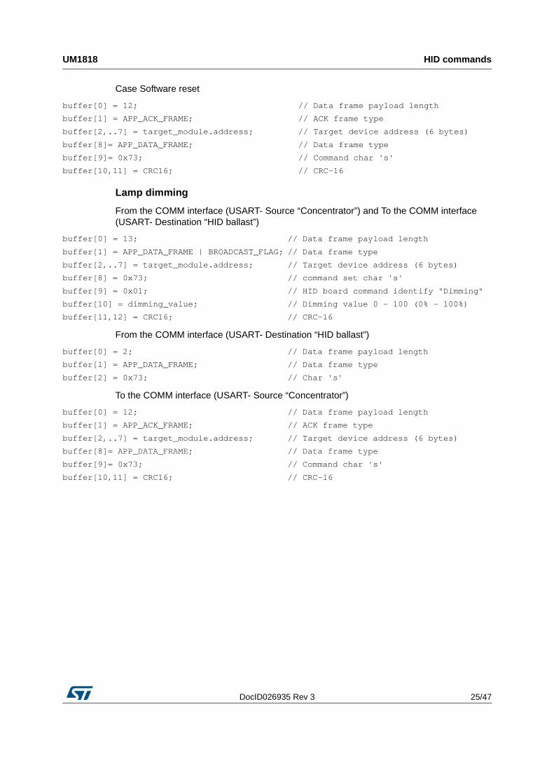
Case Software reset
Lamp dimming
From the COMM interface (USART- Source “Concentrator”) and To the COMM interface (USART- Destination “HID ballast”)
From the COMM interface (USART- Destination “HID ballast”)
To the COMM interface (USART- Source “Concentrator”)
buffer[0] = 12;
buffer[1] = APP_ACK_FRAME;
buffer[2,..7] = target_module.address;
buffer[8]= APP_DATA_FRAME;
buffer[9]= 0x73;
buffer[10,11] = CRC16;
// Data frame payload length
// ACK frame type
// Target device address (6 bytes)
// Data frame type
// Command char 's'
// CRC-16
buffer[0] = 13;
buffer[1] = APP_DATA_FRAME | BROADCAST_FLAG;
buffer[2,..7] = target_module.address;
buffer[8] = 0x73;
buffer[9] = 0x01;
buffer[10] = dimming_value;
buffer[11,12] = CRC16;
// Data frame payload length
// Data frame type
// Target device address (6 bytes)
// command set char 's'
// HID board command identify "Dimming"
// Dimming value 0 - 100 (0% - 100%)
// CRC-16
buffer[0] = 2;
buffer[1] = APP_DATA_FRAME;
buffer[2] = 0x73;
// Data frame payload length
// Data frame type
// Char 's'
buffer[0] = 12;
buffer[1] = APP_ACK_FRAME;
buffer[2,..7] = target_module.address;
buffer[8]= APP_DATA_FRAME;
buffer[9]= 0x73;
buffer[10,11] = CRC16;
// Data frame payload length
// ACK frame type
// Target device address (6 bytes)
// Data frame type
// Command char 's'
// CRC-16
HID commands UM1818
26/47 DocID026935 Rev 3
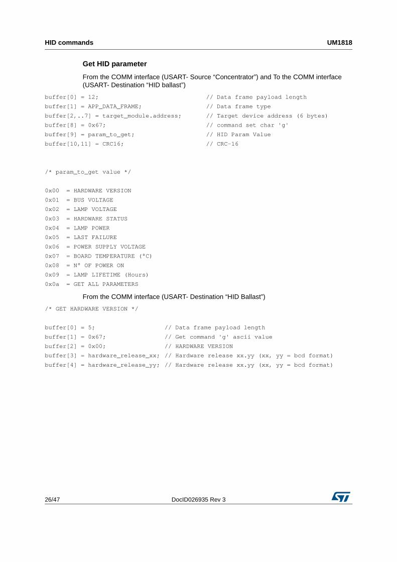
Get HID parameter
From the COMM interface (USART- Source “Concentrator”) and To the COMM interface (USART- Destination “HID ballast”)
From the COMM interface (USART- Destination “HID Ballast”)
buffer[0] = 12;
buffer[1] = APP_DATA_FRAME;
buffer[2,..7] = target_module.address;
buffer[8] = 0x67;
buffer[9] = param_to_get;
buffer[10,11] = CRC16;
/* param_to_get value */
0x00 = HARDWARE VERSION
0x01 = BUS VOLTAGE
0x02 = LAMP VOLTAGE
0x03 = HARDWARE STATUS
0x04 = LAMP POWER
0x05 = LAST FAILURE
0x06 = POWER SUPPLY VOLTAGE
0x07 = BOARD TEMPERATURE (°C)
0x08 = N° OF POWER ON
0x09 = LAMP LIFETIME (Hours)
0x0a = GET ALL PARAMETERS
// Data frame payload length
// Data frame type
// Target device address (6 bytes)
// command set char 'g'
// HID Param Value
// CRC-16
/* GET HARDWARE VERSION */
buffer[0] = 5;
buffer[1] = 0x67;
buffer[2] = 0x00;
buffer[3] = hardware_release_xx;
buffer[4] = hardware_release_yy;
// Data frame payload length
// Get command 'g' ascii value
// HARDWARE VERSION
// Hardware release xx.yy (xx, yy = bcd format)
// Hardware release xx.yy (xx, yy = bcd format)
DocID026935 Rev 3 27/47
UM1818 HID commands
47
/* GET BUS VOLTAGE */
buffer[0] = 5;
buffer[1] = 0x67;
buffer[2] = 0x01;
buffer[3] = bus_voltage_h;
buffer[4] = bus_voltage_l;
// Data frame payload length
// Get command 'g' ascii value
// BUS VOLTAGE
// High byte of bus voltage
// Low byte of bus voltage
/* GET LAMP VOLTAGE */
buffer[0] = 5;
buffer[1] = 0x67;
buffer[2] = 0x02;
buffer[3] = lamp_voltage_h;
buffer[4] = lamp_voltage_l;
// Data frame payload length
// Get command 'g' ascii value
// LAMP VOLTAGE
// High byte of lamp voltage
// Low byte of lamp voltage
/* GET HARDWARE STATUS */
buffer[0] = 5;
buffer[1] = 0x67;
buffer[2] = 0x03;
buffer[3] = hardware_status_h;
buffer[4] = hardware_status_l;
/* hardware_status value */
0x00 = IDLE
0x01,0x02,0x03 = STARTUP
0x04,0x05 = WARMUP
0x06 = RUN
0x07 = WAIT
0x08 = FAILURE
// Data frame payload length
// Get command 'g' ascii value
// HARDWARE STATUS
// High byte of hardware status
// Low byte of hardware status
HID commands UM1818
28/47 DocID026935 Rev 3
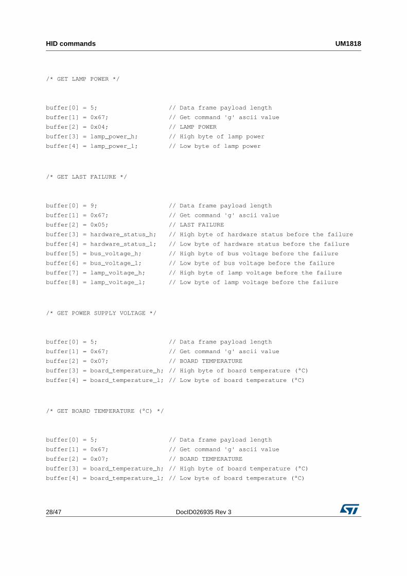
/* GET LAMP POWER */
buffer[0] = 5;
buffer[1] = 0x67;
buffer[2] = 0x04;
buffer[3] = lamp_power_h;
buffer[4] = lamp_power_l;
// Data frame payload length
// Get command 'g' ascii value
// LAMP POWER
// High byte of lamp power
// Low byte of lamp power
/* GET LAST FAILURE */
buffer[0] = 9;
buffer[1] = 0x67;
buffer[2] = 0x05;
buffer[3] = hardware_status_h;
buffer[4] = hardware_status_l;
buffer[5] = bus_voltage_h;
buffer[6] = bus_voltage_l;
buffer[7] = lamp_voltage_h;
buffer[8] = lamp_voltage_l;
// Data frame payload length
// Get command 'g' ascii value
// LAST FAILURE
// High byte of hardware status before the failure
// Low byte of hardware status before the failure
// High byte of bus voltage before the failure
// Low byte of bus voltage before the failure
// High byte of lamp voltage before the failure
// Low byte of lamp voltage before the failure
/* GET POWER SUPPLY VOLTAGE */
buffer[0] = 5;
buffer[1] = 0x67;
buffer[2] = 0x07;
buffer[3] = board_temperature_h;
buffer[4] = board_temperature_l;
// Data frame payload length
// Get command 'g' ascii value
// BOARD TEMPERATURE
// High byte of board temperature (°C)
// Low byte of board temperature (°C)
/* GET BOARD TEMPERATURE (°C) */
buffer[0] = 5;
buffer[1] = 0x67;
buffer[2] = 0x07;
buffer[3] = board_temperature_h;
buffer[4] = board_temperature_l;
// Data frame payload length
// Get command 'g' ascii value
// BOARD TEMPERATURE
// High byte of board temperature (°C)
// Low byte of board temperature (°C)
DocID026935 Rev 3 29/47
UM1818 HID commands
47
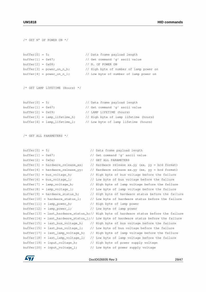
/* GET N° OF POWER ON */
buffer[0] = 5;
buffer[1] = 0x67;
buffer[2] = 0x08;
buffer[3] = power_on_n_h;
buffer[4] = power_on_n_l;
// Data frame payload length
// Get command 'g' ascii value
// N. OF POWER ON
// High byte of number of lamp power on
// Low byte of number of lamp power on
/* GET LAMP LIFETIME (Hours) */
buffer[0] = 5;
buffer[1] = 0x67;
buffer[2] = 0x09;
buffer[3] = lamp_lifetime_h;
buffer[4] = lamp_lifetime_l;
// Data frame payload length
// Get command 'g' ascii value
// LAMP LIFETIME (hours)
// High byte of lamp lifetime (hours)
// Low byte of lamp lifetime (hours)
/* GET ALL PARAMETERS */
buffer[0] = 5;
buffer[1] = 0x67;
buffer[2] = 0x0a;
buffer[3] = hardware_release_xx;
buffer[4] = hardware_release_yy;
buffer[5] = bus_voltage_h;
buffer[6] = bus_voltage_l;
buffer[7] = lamp_voltage_h;
buffer[8] = lamp_voltage_l;
buffer[9] = hardware_status_h;
buffer[10] = hardware_status_l;
buffer[11] = lamp_power_h;
buffer[12] = lamp_power_l;
buffer[13] = last_hardware_status_h;
buffer[14] = last_hardware_status_l;
buffer[15] = last_bus_voltage_h;
buffer[15] = last_bus_voltage_l;
buffer[17] = last_lamp_voltage_h;
buffer[18] = last_lamp_voltage_l;
buffer[19] = input_voltage_h;
buffer[20] = input_voltage_l;
// Data frame payload length
// Get command 'g' ascii value
// GET ALL PARAMETERS
// Hardware release xx.yy (xx, yy = bcd format)
// Hardware release xx.yy (xx, yy = bcd format)
// High byte of bus voltage before the failure
// Low byte of bus voltage before the failure
// High byte of lamp voltage before the failure
// Low byte of lamp voltage before the failure
// High byte of hardware status before the failure
// Low byte of hardware status before the failure
// High byte of lamp power
// Low byte of lamp power
// High byte of hardware status before the failure
// Low byte of hardware status before the failure
// High byte of bus voltage before the failure
// Low byte of bus voltage before the failure
// High byte of lamp voltage before the failure
// Low byte of lamp voltage before the failure
// High byte of power supply voltage
// Low byte of power supply voltage
HID commands UM1818
30/47 DocID026935 Rev 3
To the COMM interface (USART- source “concentrator”)
buffer[21] = board_temperature_h;
buffer[22] = board_temperature_l;
buffer[23] = power_on_n_h;
buffer[24] = power_on_n_l;
buffer[25] = lamp_lifetime_h;
buffer[26] = lamp_lifetime_l;
// High byte of board temperature (°C)
// Low byte of board temperature (°C)
// High byte of number of lamp power on
// Low byte of number of lamp power on
// High byte of lamp lifetime (hours)
// Low byte of lamp lifetime (hours)
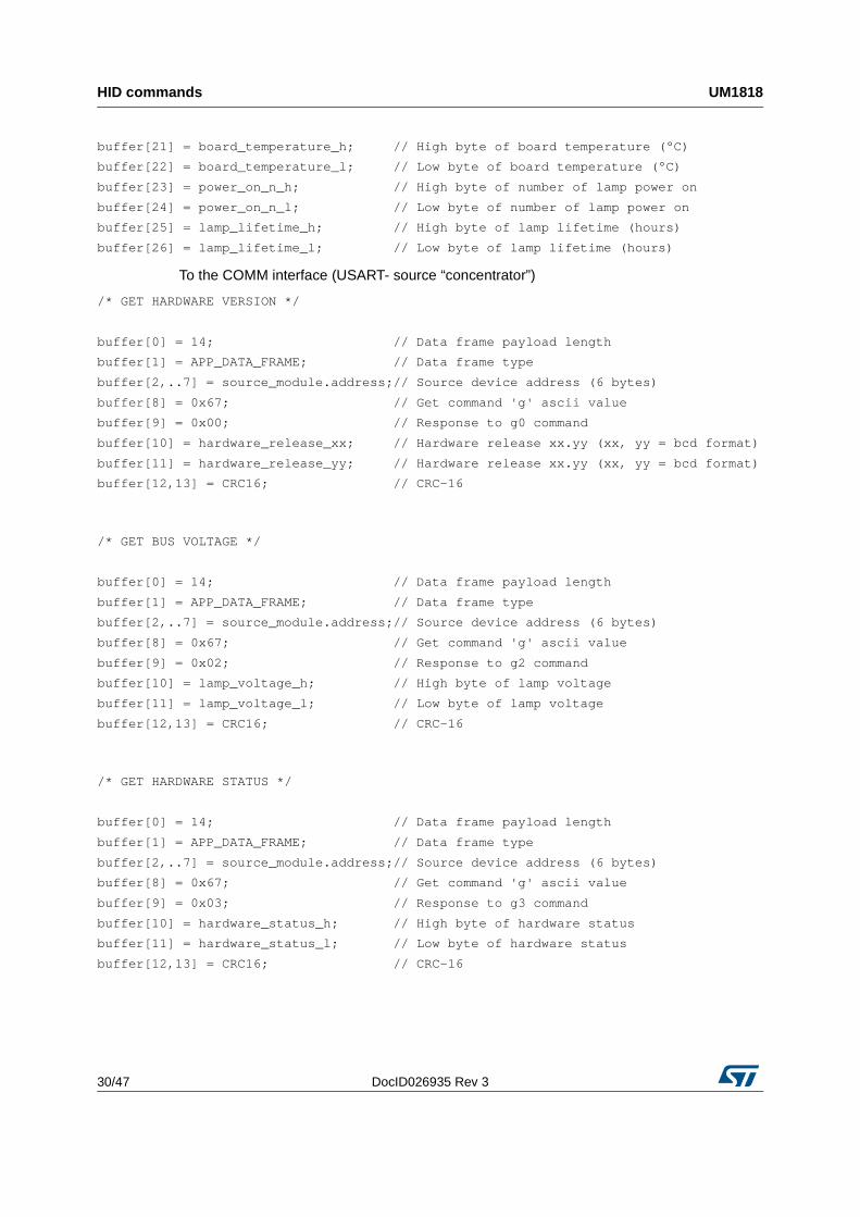
/* GET HARDWARE VERSION */
buffer[0] = 14;
buffer[1] = APP_DATA_FRAME;
buffer[2,..7] = source_module.address;
buffer[8] = 0x67;
buffer[9] = 0x00;
buffer[10] = hardware_release_xx;
buffer[11] = hardware_release_yy;
buffer[12,13] = CRC16;
// Data frame payload length
// Data frame type
// Source device address (6 bytes)
// Get command 'g' ascii value
// Response to g0 command
// Hardware release xx.yy (xx, yy = bcd format)
// Hardware release xx.yy (xx, yy = bcd format)
// CRC-16
/* GET BUS VOLTAGE */
buffer[0] = 14;
buffer[1] = APP_DATA_FRAME;
buffer[2,..7] = source_module.address;
buffer[8] = 0x67;
buffer[9] = 0x02;
buffer[10] = lamp_voltage_h;
buffer[11] = lamp_voltage_l;
buffer[12,13] = CRC16;
// Data frame payload length
// Data frame type
// Source device address (6 bytes)
// Get command 'g' ascii value
// Response to g2 command
// High byte of lamp voltage
// Low byte of lamp voltage
// CRC-16
/* GET HARDWARE STATUS */
buffer[0] = 14;
buffer[1] = APP_DATA_FRAME;
buffer[2,..7] = source_module.address;
buffer[8] = 0x67;
buffer[9] = 0x03;
buffer[10] = hardware_status_h;
buffer[11] = hardware_status_l;
buffer[12,13] = CRC16;
// Data frame payload length
// Data frame type
// Source device address (6 bytes)
// Get command 'g' ascii value
// Response to g3 command
// High byte of hardware status
// Low byte of hardware status
// CRC-16
DocID026935 Rev 3 31/47
UM1818 HID commands
47
/* hardware_status value */
0x00
0x01,0x02,0x03
0x04,0x05
0x06
0x07
0x08
= IDLE
= STARTUP
= WARMUP
= RUN
= WAIT
= FAILURE
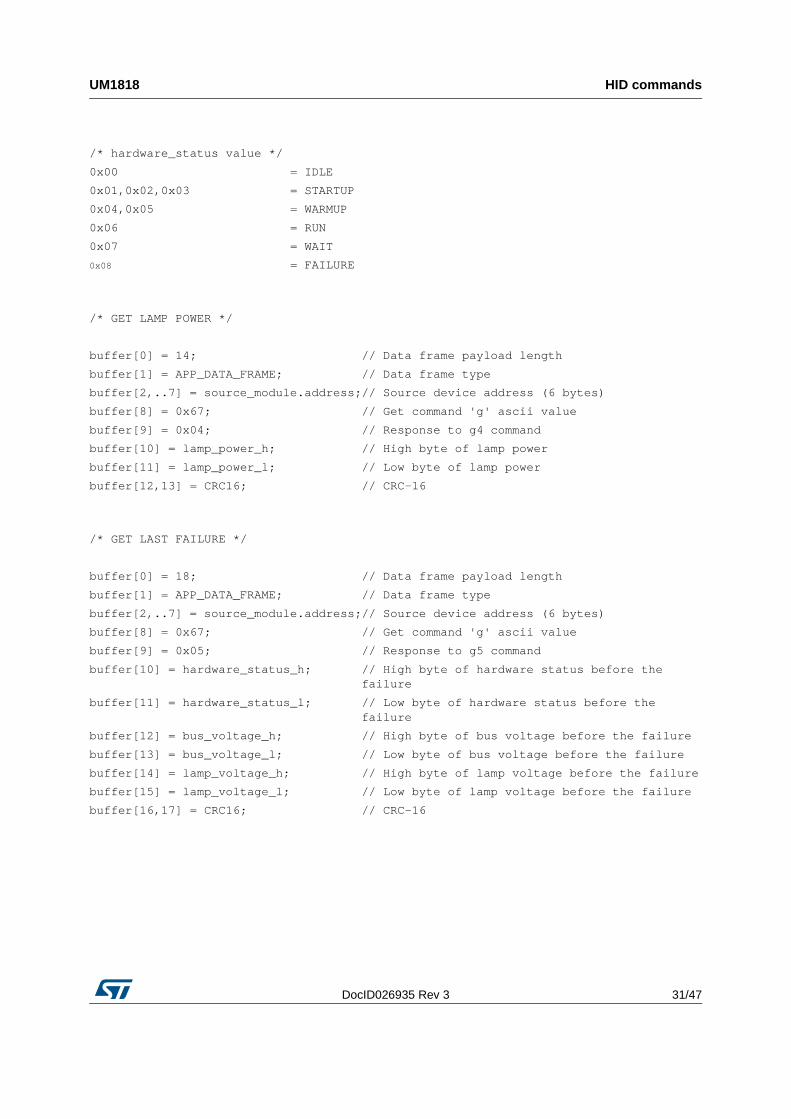
/* GET LAMP POWER */
buffer[0] = 14;
buffer[1] = APP_DATA_FRAME;
buffer[2,..7] = source_module.address;
buffer[8] = 0x67;
buffer[9] = 0x04;
buffer[10] = lamp_power_h;
buffer[11] = lamp_power_l;
buffer[12,13] = CRC16;
// Data frame payload length
// Data frame type
// Source device address (6 bytes)
// Get command 'g' ascii value
// Response to g4 command
// High byte of lamp power
// Low byte of lamp power
// CRC-16
/* GET LAST FAILURE */
buffer[0] = 18;
buffer[1] = APP_DATA_FRAME;
buffer[2,..7] = source_module.address;
buffer[8] = 0x67;
buffer[9] = 0x05;
buffer[10] = hardware_status_h;
buffer[11] = hardware_status_l;
buffer[12] = bus_voltage_h;
buffer[13] = bus_voltage_l;
buffer[14] = lamp_voltage_h;
buffer[15] = lamp_voltage_l;
buffer[16,17] = CRC16;
// Data frame payload length
// Data frame type
// Source device address (6 bytes)
// Get command 'g' ascii value
// Response to g5 command
// High byte of hardware status before the failure
// Low byte of hardware status before the failure
// High byte of bus voltage before the failure
// Low byte of bus voltage before the failure
// High byte of lamp voltage before the failure
// Low byte of lamp voltage before the failure
// CRC-16
HID commands UM1818
32/47 DocID026935 Rev 3
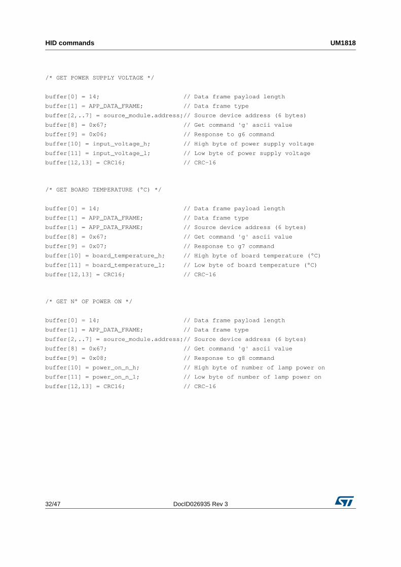
/* GET POWER SUPPLY VOLTAGE */
buffer[0] = 14;
buffer[1] = APP_DATA_FRAME;
buffer[2,..7] = source_module.address;
buffer[8] = 0x67;
buffer[9] = 0x06;
buffer[10] = input_voltage_h;
buffer[11] = input_voltage_l;
buffer[12,13] = CRC16;
// Data frame payload length
// Data frame type
// Source device address (6 bytes)
// Get command 'g' ascii value
// Response to g6 command
// High byte of power supply voltage
// Low byte of power supply voltage
// CRC-16
/* GET BOARD TEMPERATURE (°C) */
buffer[0] = 14;
buffer[1] = APP_DATA_FRAME;
buffer[1] = APP_DATA_FRAME;
buffer[8] = 0x67;
buffer[9] = 0x07;
buffer[10] = board_temperature_h;
buffer[11] = board_temperature_l;
buffer[12,13] = CRC16;
// Data frame payload length
// Data frame type
// Source device address (6 bytes)
// Get command 'g' ascii value
// Response to g7 command
// High byte of board temperature (°C)
// Low byte of board temperature (°C)
// CRC-16
/* GET N° OF POWER ON */
buffer[0] = 14;
buffer[1] = APP_DATA_FRAME;
buffer[2,..7] = source_module.address;
buffer[8] = 0x67;
buffer[9] = 0x08;
buffer[10] = power_on_n_h;
buffer[11] = power_on_n_l;
buffer[12,13] = CRC16;
// Data frame payload length
// Data frame type
// Source device address (6 bytes)
// Get command 'g' ascii value
// Response to g8 command
// High byte of number of lamp power on
// Low byte of number of lamp power on
// CRC-16
DocID026935 Rev 3 33/47
UM1818 HID commands
47
/* GET LAMP LIFETIME (Hours) */
buffer[0] = 14;
buffer[1] = APP_DATA_FRAME;
buffer[2,..7] = source_module.address;
buffer[8] = 0x67;
buffer[9] = 0x09;
buffer[10] = lamp_lifetime_h;
buffer[11] = lamp_lifetime_l;
buffer[12,13] = CRC16;
// Data frame payload length
// Data frame type
// Source device address (6 bytes)
// Get command 'g' ascii value
// Response to g9 command
// High byte of lamp lifetime (hours)
// Low byte of lamp lifetime (hours)
// CRC-16
/* GET ALL PARAMETERS */
buffer[0] = 36;
buffer[1] = APP_DATA_FRAME;
buffer[2,..7] = source_module.address;
buffer[8] = 0x67;
buffer[9] = 0x0a;
buffer[10] = hardware_release_xx;
buffer[11] = hardware_release_yy;
buffer[12] = bus_voltage_h;
buffer[13] = bus_voltage_l;
buffer[14] = lamp_voltage_h;
buffer[15] = lamp_voltage_l;
buffer[16] = hardware_status_h;
buffer[17] = hardware_status_l;
buffer[18] = lamp_power_h;
buffer[19] = lamp_power_l;
buffer[20] = last_hardware_status_h;
buffer[21] = last_hardware_status_l;
// Data frame payload length
// Data frame type
// Source device address (6 bytes)
// Get command 'g' ascii value
// Response to g10 command
// Hardware release xx.yy (xx, yy = bcd format)
// Hardware release xx.yy (xx, yy = bcd format)
// High byte of bus voltage before the failure
// Low byte of bus voltage before the failure
// High byte of lamp voltage before the failure
// Low byte of lamp voltage before the failure
// High byte of hardware status before the failure
// Low byte of hardware status before the failure
// High byte of lamp power
// Low byte of lamp power
// High byte of hardware status before the failure
// Low byte of hardware status before the failure
HID commands UM1818
34/47 DocID026935 Rev 3
If an error occurs from the HID board or from the network, the following frame throughout the COMM will be sent:
buffer[22] = last_bus_voltage_h;
buffer[23] = last_bus_voltage_l;
buffer[24] = last_lamp_voltage_h;
buffer[25] = last_lamp_voltage_l;
buffer[26] = input_voltage_h;
buffer[27] = input_voltage_l;
buffer[28] = board_temperature_h;
buffer[29] = board_temperature_l;
buffer[30] = power_on_n_h;
buffer[31] = power_on_n_l;
buffer[32] = lamp_lifetime_h;
buffer[33] = lamp_lifetime_l;
buffer[34,35] = CRC16;
// High byte of bus voltage before the failure
// Low byte of bus voltage before the failure
// High byte of lamp voltage before the failure
// Low byte of lamp voltage before the failure
// High byte of power supply voltage
// Low byte of power supply voltage
// High byte of board temperature (°C)
// Low byte of board temperature (°C)
// High byte of number of lamp power on
// Low byte of number of lamp power on
// High byte of lamp lifetime (hours)
// Low byte of lamp lifetime (hours)
// CRC-16
/* ERROR FRAME RESPONSE */
buffer[0] = 12;
buffer[1] = APP_ERROR_FRAME;
buffer[4,5,6,7] = target_module.address;
buffer[8,9] = HID_error_code;
buffer[10,11] = CRC16;
/* HID_error_code value */
0x10 = HID response error
0x11 = HID command unknown
0x12 = HID board response timeout
0x13 = HID packet delivery impossible
// Error frame payload length
// Error frame type
// Target device address (6 bytes)
// HID board error code (2 bytes)
// CRC-16
DocID026935 Rev 3 35/47
UM1818 Schematic diagrams and bill of material
47
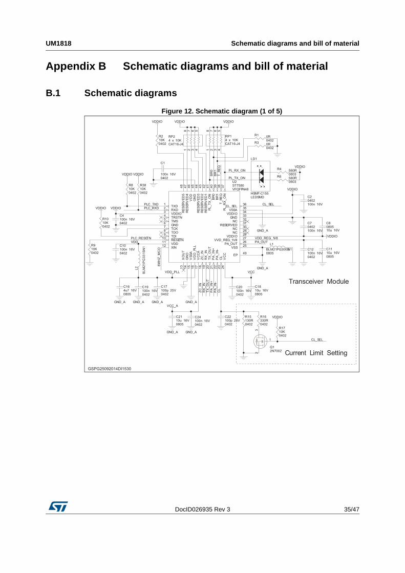
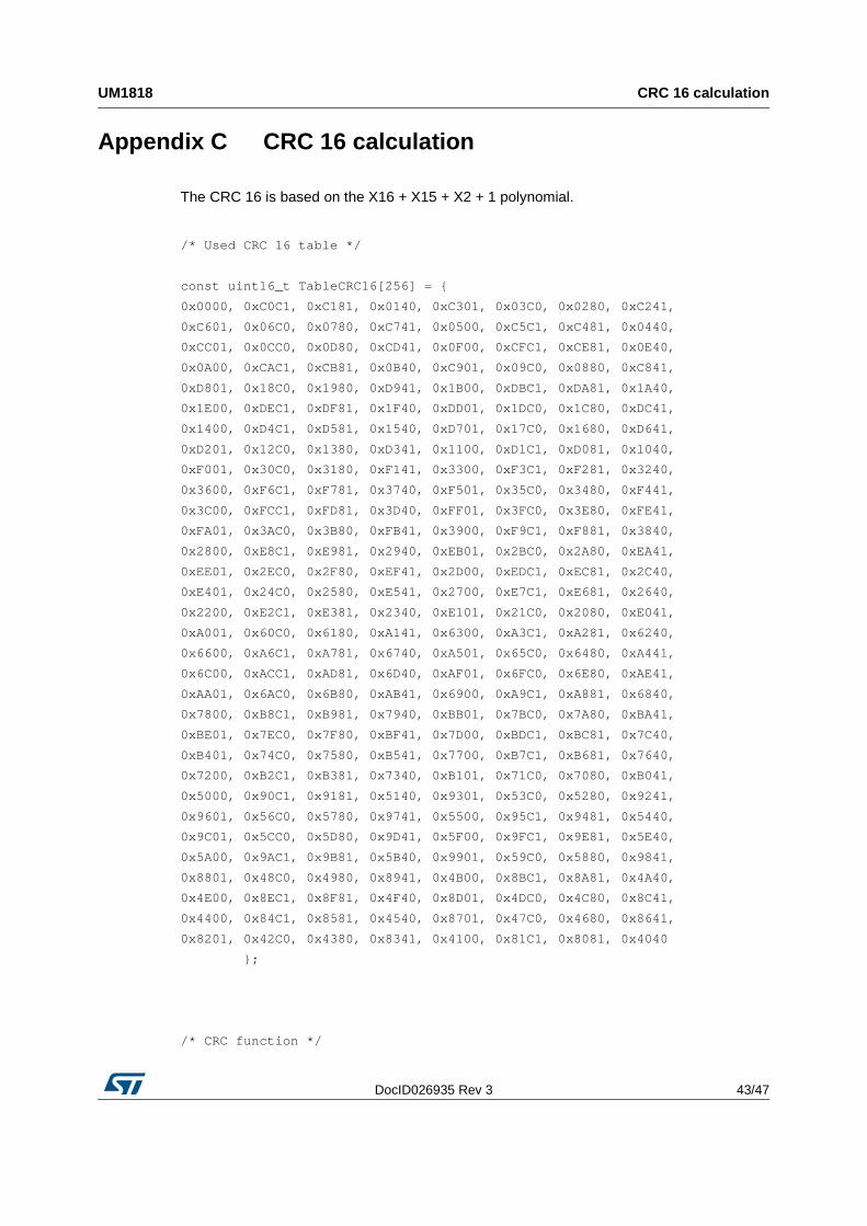
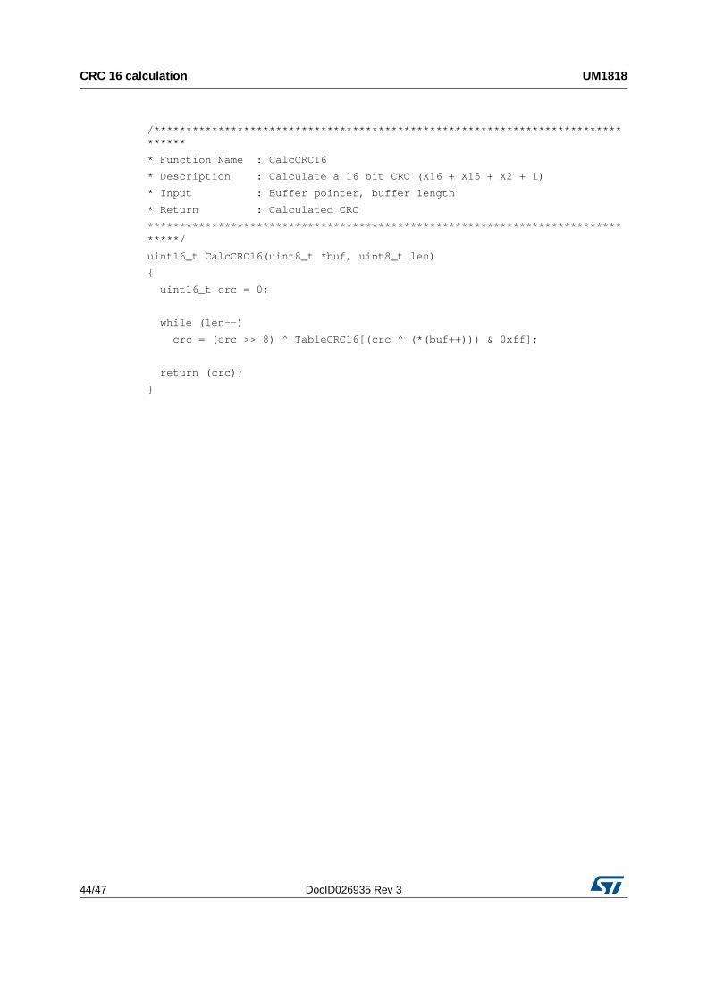
Appendix B Schematic diagrams and bill of material
B.1 Schematic diagrams
Figure 12. Schematic diagram (1 of 5)
VFQFPN48
EP49
TXD1
RXD23
VDDIO4
TRSTN5
TMS6
GNDTCK
78
TDO9
TDIRESETN
10
VDD11
XIN12
13
X G V VSO N D
SU D DA _T
PL
LV Z
CC_C IA N
RX
_IN
TX
_O
UT
PA
_IN
+P
A_
IN-
C VL C
C
VSSPA_OUT
25
14
15
16
17
18
19
20
21
22
23
24
VVD_
REP
L_
S
RE
E
G_VDDI
VDDIVS
G
1
RVED
S
ND
NCNC
NC
V8O
OA
2
3
3
23
33
228
4
1
90
23
67
CL_SEL3365
RX
_O
N
47
46
45
44
43
42
41
40
39
38
37
T_
RBBRR EQ10
U2ST7580
RRRRR
EEEEE PL
_S
ES
ES
E
SE
SE TRRRRR
XVVVVV GV _EEEEE ND ODDDDD
NDD 123454
8
LEDSMD
LD1
HSMF-C155
0603
R4 560R
0603
R6 560R
VDDIO
BR
0B
R1
CAT16-J4
1 2 3 4
8 7 6 5
RP14 x 10K
VDDIO
PLC_RXDPLC_TXD
0402
C4
VDDIO
100n 16V
8M
HZ
_M
CO
0402
C10100n 16V
L2
0805
BL
M2
1P
G3
31
SN
1
C164u7 16V
GND_A GND_A
0402
C19100n 16V
GND_A
0402
C17100p 25V
GND_A
0402
C24100n 16V
GND_A
0805
C2110u 16V
GND_A
VCC_A
VDD_PLL
0402
C20100n 16V
0805
C1810u 16VZ
C_
INR
X_
INT
X_
OU
TP
A_
IN+
CL
PA
_IN
-
VCC
0402
C22100p 25V
0402
R15130R
0402
R16330R
1
23
Q12N7002
0402
R1710K
VDDIO
CL_SEL
CL_SEL
GND_A
0805
L1
BLM21PG300SN1
PL_RX_ON
PL_TX_ON
PA_OUTVDD
0402
R1010K
VDDIO
PLC_RESETN
0402
C12100n 16V
0805
C1110u 16V
VDD_REG_1V8
0402C7
0805100n 16V
C8
10u 16V
VDDIO
0402C2
100n 16V
GND_A
VDDIO
Current Limit Setting
CAT16-J4
1 2 3 4
8 7 6 5
RP24 x 10K
0402
C1
100n 16V
0402
R210K
VDDIO VDDIO
0402
R910K
0402
R810K
VDDIO
Transceiver Module
0402
R3 0R0402
R1 0R
T_
RE
Q
0402
R3810K
VDDIO
GSPG25092014DI1530
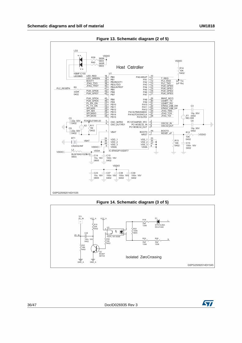
Schematic diagrams and bill of material UM1818
36/47 DocID026935 Rev 3
Figure 13. Schematic diagram (2 of 5)
Figure 14. Schematic diagram (3 of 5)
BOOT0744
NRST
56
OSC_IN/PD0OSC_OUT/PD1
PA0-WKUP1101
PA931
PA1032
PA1133
PA1234
PA13/JTMS/SWDIO37
PA15/JTDI
PA112
PA14/JTCK/SWCLK38
PA213
PA314
PA415
PA516
PA7PA6
17
PA82390
23
1109
89
PPP
B0B1B2/BOOT1
40PB3/JTDOPB4/JNTRSTPB5
41
PB642
PB743
2346
VDD_1
48VDD_2
9VDD_3VDDA
VSS_12335
VSS_247
VSSAVSS_3
8
PB845
PB946
PB1021
PB1122
PB1225
PB1326
PB1427
PB1528
1VBAT
PC13/TAMPER_RTC23
U1
PC15/OSC32_OUTPC14/OSC32_IN
4
IC-STM32F103CBT7
X20402
FOXSDLF/080-20C5
22p 50V
0402
C922p 50V
VDDIO
PL_RX_ONPL_TX_ON
PLC_RESETN
JTAG_TDOJTAG_TRST
JTAG_TCKJTAG_TDI
JTAG_TMS
OSC32_INOSC32_OUT
0402
C15100n 16V
0603
L3 VDDA
0805
BLM18AG102SN1DC14
VDDIO
10u 16V
BT1
CR2032/1HF
VBAT
0402
R5
330R
PLC_RXDPLC_TXD
T_REQ
PLM_GPIO0PLM_GPIO1PLM_GPIO2PLM_GPIO3
PLM_GPIO4PLM_GPIO5
PLM_GPIO6
BOOT1
PLM_GPIO7
8MHZ_MCOUSART_TXUSART_RXSTM32_USB_DMSTM32_USB_DP
SPI_MOSISPI_MISOSPI_SCK
BOOT0
SPI_NSS
0402
R1310K
0402
C13100n 16V
0402
R12
10KVDDIO
0402
R111M
Host Controller
X1MC-306
0402
C3
10p 50V
0402
C6
10p 50V
0402
C37100n 16V
0805
C2310u 16V
0402
C38100n 16V
VDDIO
0402
C39100n 16V
0402
R1410K
VDDIO
RESET_uP
(uP Tx)(uP Rx)
VDDIO
0603
R39 560R
0603
R40 560R
LEDSMD
LD2
HSMF-C155LED_REDLED_GREEN
GSPG25092014DI1535
0402
C29
100n 16V
1206
R18
33K
1206
R25
33K1206
R26
33K
SOT23
Q2BC847
0402
R1922K
0402
R3210M
1
2
4
3
U3
0402
HCPL-181-000E
R3033K
VCC_A VCC_A
ZC_IN
GND_AGND_A
L
N
Isolated Zero Crossing
DO-214AC
D1
STTH1L06A
0805
R22100K
1
TP1ZC_IN
GSPG25092014DI1545
DocID026935 Rev 3 37/47
UM1818 Schematic diagrams and bill of material
47
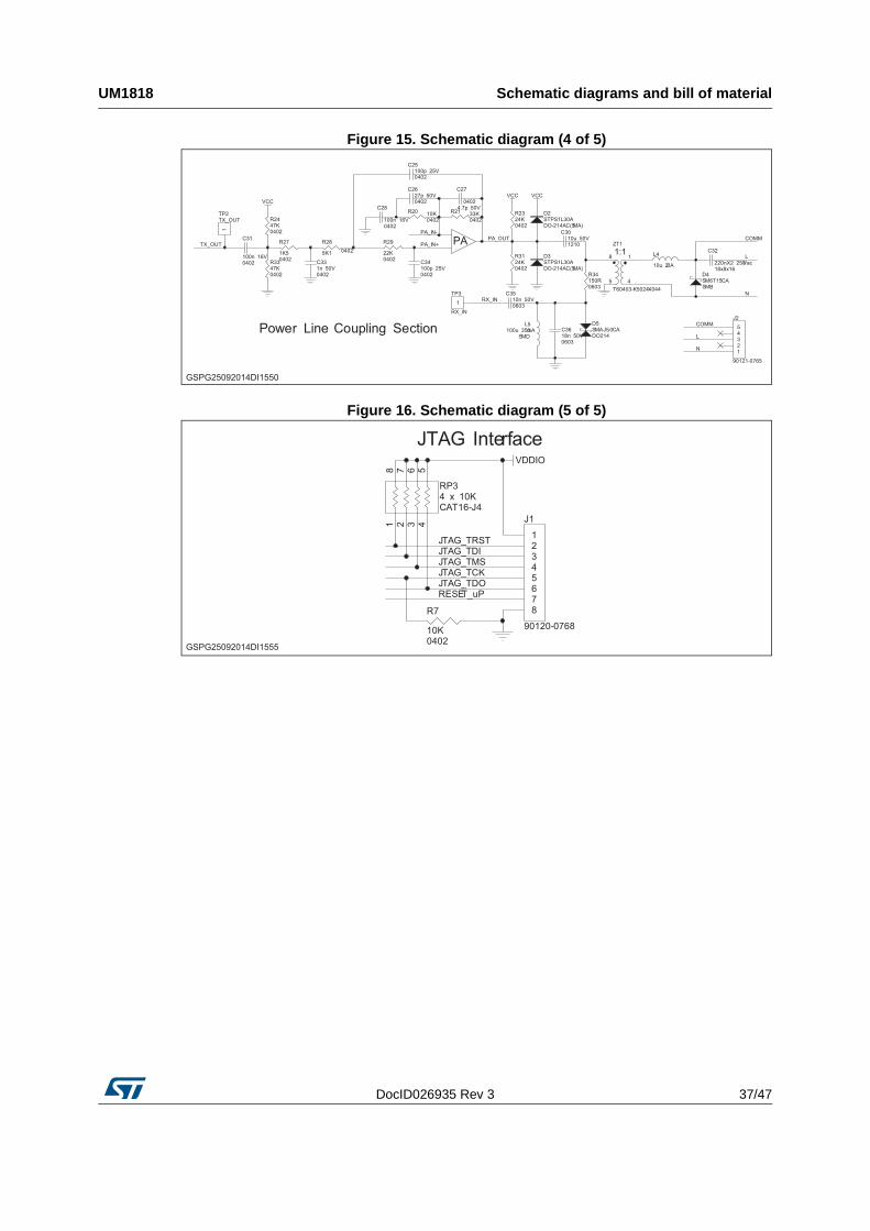
Figure 15. Schematic diagram (4 of 5)
Figure 16. Schematic diagram (5 of 5)
18x8x16
C32
220n X2 250Vac
L41
4
10u 2.0A
8
5
1:1ZT1
SMB
D4
T60403-K5024-X044
SM6T15CA0603
R34150R
DO214
D5SMAJ5.0CA
0603
C36
SMD 18n 50V
L5100u 350mA
0603
C3510n 50V
1210
C3010u 50V
D3
DO-214AC(SMA)STPS1L30A
D2
DO-214AC(SMA)
VCC
STPS1L30A0402
R2324K
0402
R3124K
VCC
PA_OUT
0402
R21 33K
PAPA_IN+
PA_IN-
0402
R20 10K
0402
C28
100n 16V
0402
R29
22K
0402
C34100p 25V
0402
R28
5K10402
R27
1K5
0402
C25100p 25V
0402
C2627p 50V
0402
C27
4.7p 50V
0402
C331n 50V
0402
R2447K
0402
R3347K
0402
C31
VCC
100n 16V
TX_OUT
L
N
COMM
123
Power Line Coupling Section 45
J2
L
N
COMM
90121-0765
RX_IN
1
TP2TX_OUT
1
TP3
RX_IN
GSPG25092014DI1550
J1
12345678
90120-0768
CAT16-J4
1 2 3 4
8 7 6 5
RP34 x 10K
0402
R7
10K
JTAG_TCK
JTAG_TDI
JTAG_TDO
JTAG_TMS
JTAG_TRST
RESET_uP
VDDIO
JTAG Interface
GSPG25092014DI1555
Schem
atic diagrams and bill of m
aterialU
M1818
38/47D
ocID026935 R
ev 3
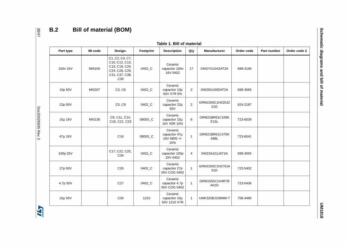
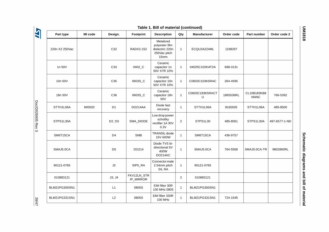
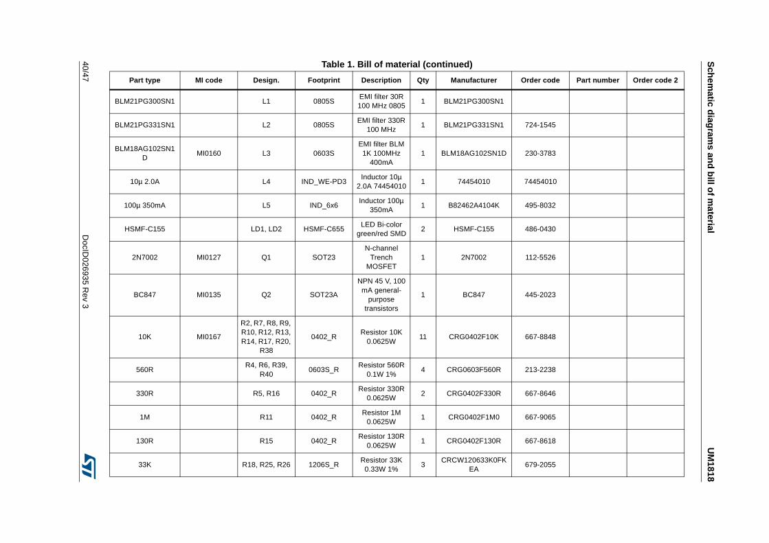
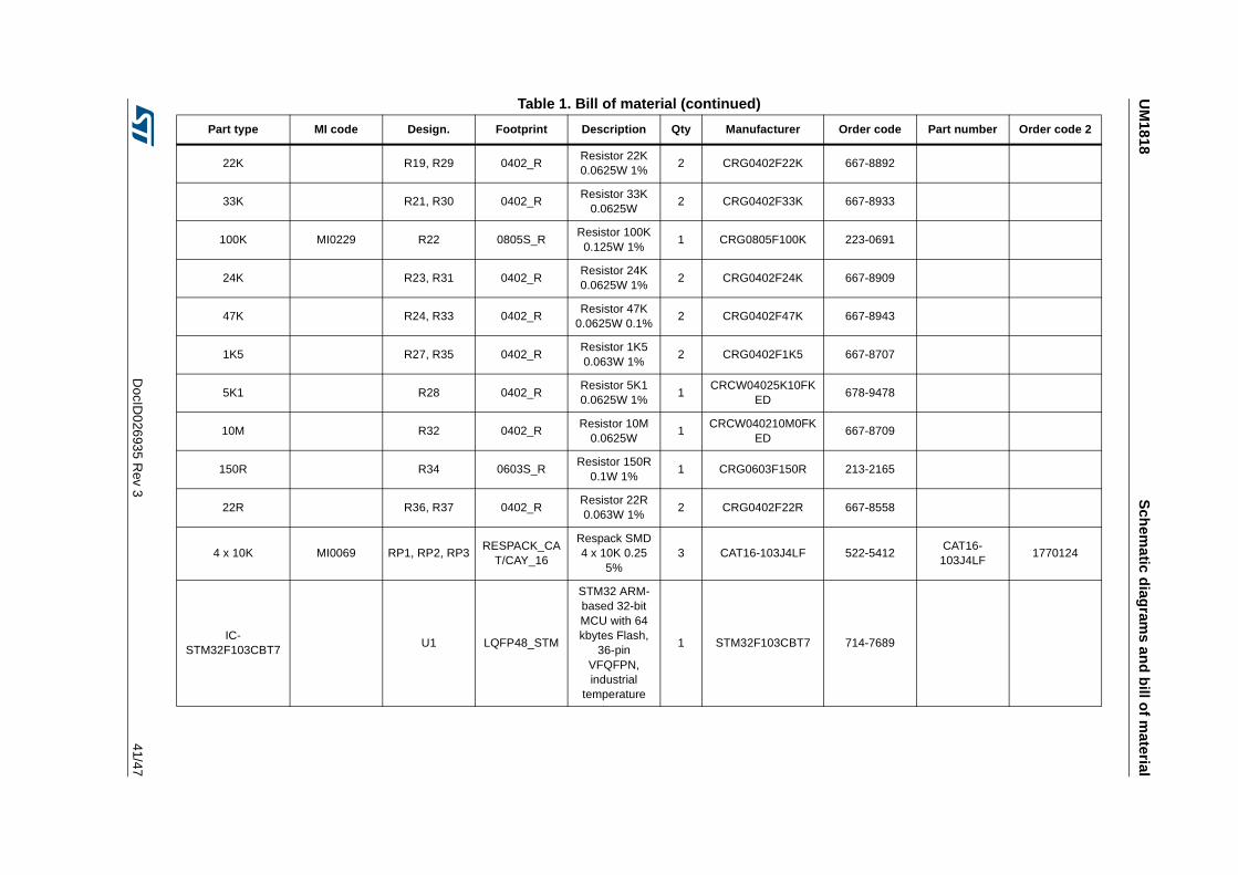
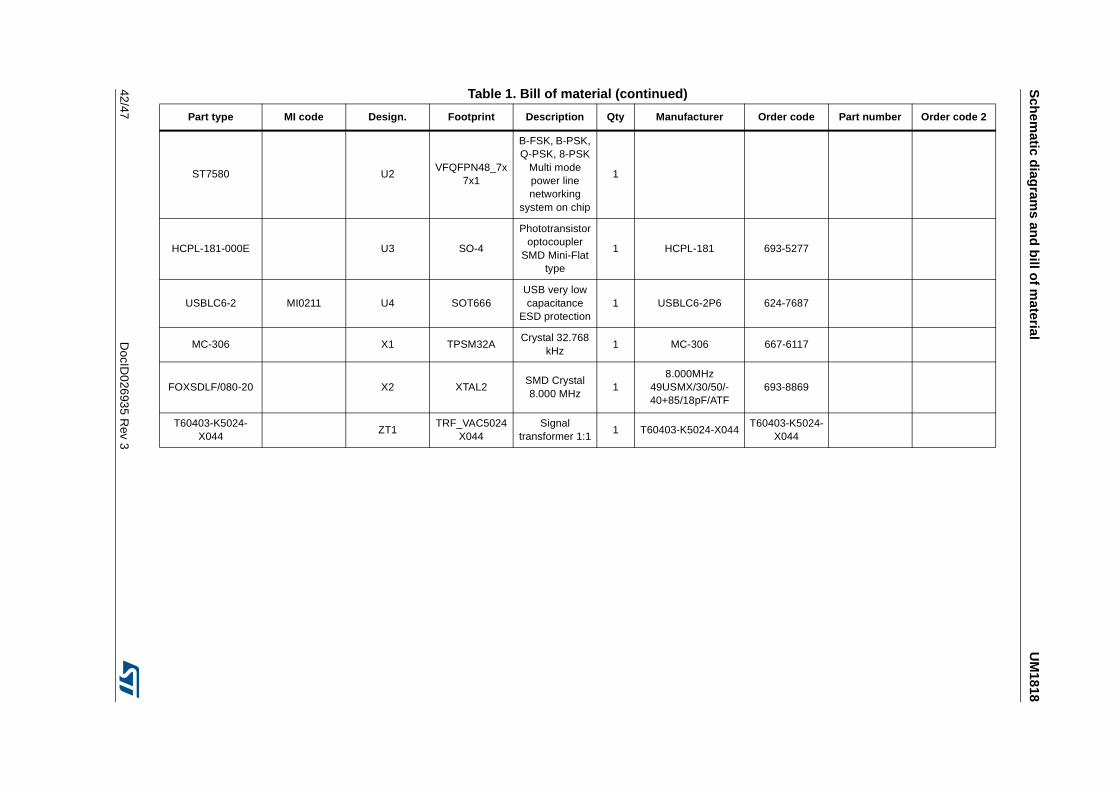
B.2 Bill of material (BOM)
Table 1. Bill of material
Part type MI code Design. Footprint Description Qty Manuf acturer Order code Part number Order code 2
STMicroelectronics NV and its subsidiaries (“ST”) reserve the right to make changes, corrections, enhancements, modifications, and improvements to ST products and/or to this document at any time without notice. Purchasers should obtain the latest relevant information on ST products before placing orders. ST products are sold pursuant to ST’s terms and conditions of sale in place at the time of order acknowledgement.
Purchasers are solely responsible for the choice, selection, and use of ST products and ST assumes no liability for application assistance or the design of Purchasers’ products.
No license, express or implied, to any intellectual property right is granted by ST herein.
Resale of ST products with provisions different from the information set forth herein shall void any warranty granted by ST for such product.
ST and the ST logo are trademarks of ST. All other product or service names are the property of their respective owners.
Information in this document supersedes and replaces information previously supplied in any prior versions of this document.