Page 1
Unclassified ENV/JM/MONO(2015)5 Organisation de Coopération et de Développement Économiques Organisation for Economic Co-operation and Development 03-Apr-2015
___________________________________________________________________________________________
_____________ English - Or. English ENVIRONMENT DIRECTORATE
JOINT MEETING OF THE CHEMICALS COMMITTEE AND
THE WORKING PARTY ON CHEMICALS, PESTICIDES AND BIOTECHNOLOGY
EMISSION SCENARIO DOCUMENT (ESD) ON CHEMICAL VAPOUR DEPOSITION IN THE
SEMICONDUCTOR INDUSTRY
Series on Emission Scenario Documents
No. 35
Mr Takahiro Hasegawa
Telephone: +(33-1) 45 24 79 07
Email: [email protected]
JT03373666
Complete document available on OLIS in its original format
This document and any map included herein are without prejudice to the status of or sovereignty over any territory, to the delimitation of
international frontiers and boundaries and to the name of any territory, city or area.
EN
V/JM
/MO
NO
(20
15
)5
Un
classified
En
glish
- Or. E
ng
lish
Cancels & replaces the same document of 02 April 2015
Page 2
ENV/JM/MONO/(2015)5
2
Page 3
ENV/JM/MONO/(2015)5
3
OECD Environment, Health and Safety Publications
Series on Emission Scenario Documents
No. 35
EMISSION SCENARIO DOCUMENT (ESD) ON CHEMICAL VAPOUR DESPOSITION
IN THE SEMICONDUCTOR INDUSTRY
Environment Directorate
ORGANISATION FOR ECONOMIC CO-OPERATION AND DEVELOPMENT
Paris 2015
Page 4
ENV/JM/MONO/(2015)5
4
Also published in the Series on Emission Scenario Documents:
No. 1, Guidance Document on Emission Scenario Documents (2000)
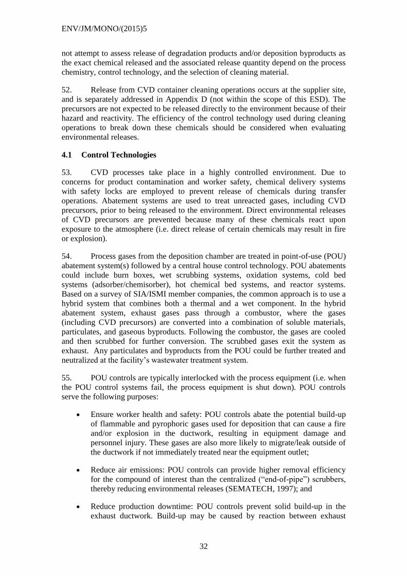
No. 2, Emission Scenario Document for Wood preservatives (2000)
No. 3, Emission Scenario Document on Plastic Additives
(2004; revised in 2009)
No. 4, Emission Scenario Document on Water Treatment Chemicals (2004)
No. 5, Emission Scenario Document on Photographic Industry (2004)
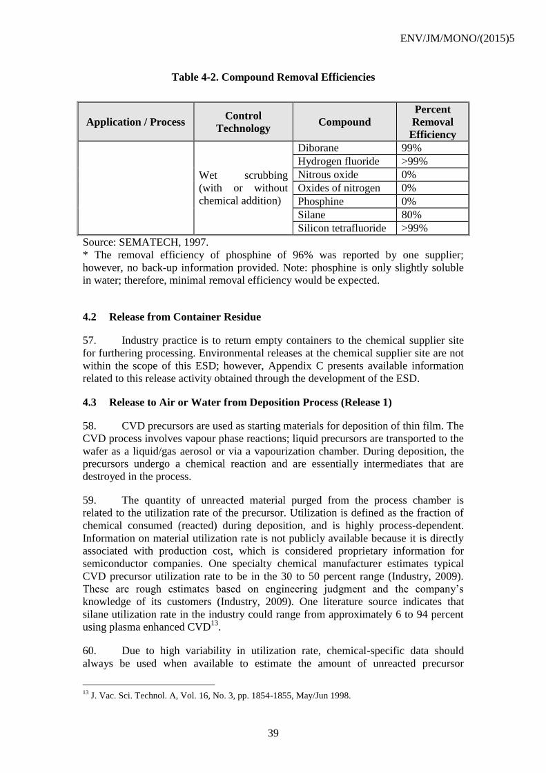
No. 6, Emission Scenario Document on Rubber Additives (2004)
No. 7, Emission Scenario Document on Textile Finishing (2004)
No. 8, Emission Scenario Document on Leather Processing (2004)
No. 9, Emission Scenario Document on Photoresist Use in Semiconductor
Manufacturing (2004; revised in 2010)
No. 10, Emission Scenario Document on Lubricants and Lubricant Additives (2004)
No. 11, Emission Scenario Document on Automotive spray application (2004)
No. 12, Emission Scenario Document on Metal finishing (2004)
No. 13, Emission Scenario Document on Antifoulants main document (2005)
No. 14, Emission Scenario Document on Insecticides for Stables and Manure Storage
Systems (2006)
No. 15, Emission Scenario Document on Kraft Pulp Mills (2006)
No. 16, Emission Scenario Document on Non-Integrated Paper Mills (2006)
No. 17, Emission Scenario Document on Recovered Paper Mills (2006)
No. 18, Emission Scenario Document for Insecticides, Acaricides and Products to
Control Other Arthropods for Household and Professional Uses (2008)
No. 19, Complementing Guideline for Writing Emission Scenario Documents: The
Life-Cycle Step “service-life”(2009)
No. 20, Emission Scenario Document on Adhesive Formulation (2009)
Page 5
ENV/JM/MONO/(2015)5
5
No. 21, Emission Scenario Document on the Formulation of Radiation Curable
Coating, Inks, and Adhesives (2009, revised 2010)
No. 22, Emission Scenario Document on Coating Industry (Paints, Lacquers and
Varnishes) (2009)
No. 23, Emission Scenario Document on Pulp, Paper and Board Industry (2009)
No. 24, Emission Scenario Document on Transport and Storage of Chemicals (2009)
No. 25, Emission Scenario Document for Chemicals Used in the Electronics
Industry (2010)
No. 26, Emission Scenario Document on the Blending of Fragrance Oils into Commercial and
Consumer Products (2010)
No. 27, Emission Scenario Document on Radiation Curable Coating, Inks and Adhesives (2011)
No. 28, Emission Scenario Document on the Use of Metalworking Fluids (2011)
No. 29, Emission Scenario Document on the Chemicals Used in Water Based Washing
Operations at Industrial and Institutional Laundries (2011)
No. 30, Emission Scenario Document on the Chemical Industry (2011)
No. 31, Emission Scenario Document on the Chemicals used in oil well production (2012)
No. 32, Emission Scenario Document on Formulation and Application of Thermal and
Carbonless Copy Paper
No. 33, Emission Scenario Document on Industrial use of industrial cleaners
No. 34, Emission Scenario Document on Use Of Adhesives
No. 35, Emission Scenario Document on Chemical Vapour Deposition In The Semiconductor
Industry
Page 6
ENV/JM/MONO/(2015)5
6
ABOUT THE OECD
The Organisation for Economic Co-operation and Development (OECD) is an intergovernmental
organisation in which representatives of 34 industrialised countries in North and South America,
Europe and the Asia and Pacific region, as well as the European Commission, meet to co-ordinate
and harmonise policies, discuss issues of mutual concern, and work together to respond to
international problems. Most of the OECD’s work is carried out by more than 200 specialised
committees and working groups composed of member country delegates. Observers from several
countries with special status at the OECD, and from interested international organisations, attend
many of the OECD’s workshops and other meetings. Committees and working groups are served
by the OECD Secretariat, located in Paris, France, which is organised into directorates and
divisions.
The Environment, Health and Safety Division publishes free-of-charge documents in 11 different
series: Testing and Assessment; Good Laboratory Practice and Compliance Monitoring;
Pesticides; Biocides; Risk Management; Harmonisation of Regulatory Oversight in
Biotechnology; Safety of Novel Foods and Feeds; Chemical Accidents; Pollutant Release and
Transfer Registers; Emission Scenario Documents; and Safety of Manufactured
Nanomaterials. More information about the Environment, Health and Safety Programme and
EHS publications is available on the OECD’s World Wide Web site
(www.oecd.org/chemicalsafety/).
This publication was developed in the IOMC context. The contents do not necessarily reflect the
views or stated policies of individual IOMC Participating Organisations.
The Inter-Organisation Programme for the Sound Management of Chemicals (IOMC) was
established in 1995 following recommendations made by the 1992 UN Conference on
Environment and Development to strengthen co-operation and increase international co-
ordination in the field of chemical safety. The Participating Organisations are FAO, ILO, UNDP,
UNEP, UNIDO, UNITAR, WHO, World Bank and OECD. The purpose of the IOMC is to
promote co-ordination of the policies and activities pursued by the Participating Organisations,
jointly or separately, to achieve the sound management of chemicals in relation to human health
and the environment.
Page 7
ENV/JM/MONO/(2015)5
7
This publication is available electronically, at no charge.
For this and many other Environment,
Health and Safety publications, consult the OECD’s
World Wide Web site (www.oecd.org/chemicalsafety/)
or contact:
OECD Environment Directorate,
Environment, Health and Safety Division
2 rue André-Pascal
75775 Paris Cedex 16
France
Fax: (33-1) 44 30 61 80
E-mail: [email protected]
© OECD 2015
Applications for permission to reproduce or translate all or part of this material
should be made to: Head of Publications Service, [email protected] , OECD, 2
rue André-Pascal, 75775 Paris Cedex 16, France
Page 8
ENV/JM/MONO/(2015)5
8
EXPLANATORY NOTES
Purpose and background
This Organisation for Economic Co-operation and Development (OECD) Emission Scenario
Document (ESD) is intended to provide information on the sources, use patterns, and potential
release pathways of chemicals used as chemical vapour deposition (CVD) precursors in the
semiconductor industry. The document presents standard approaches for estimating environmental
releases and occupational exposures, and discusses the typical engineering controls used to
mitigate exposure to CVD precursors.
This ESD may be periodically updated to reflect changes in the industry and new information
available, and extended to cover the industry area in countries other than the lead (the United
States). Users of the document are encouraged to submit comments, corrections, updates, and new
information to the OECD Environment, Health and Safety Division
([email protected] ). The comments received will be forwarded to the OECD Task
Force on Exposure Assessment, which will review the comments every two years so that the lead
country can update the document. Submitted information will also be made available to users
within the OECD web site (www.oecd.org/env/riskassessment).
How to use this document
This document may be used to provide conservative, screening-level estimates of
environmental releases of and occupational exposures to both volatile and nonvolatile chemicals
used in CVD. Some estimates might result in release and exposure amounts that are likely to be
higher, or at least higher than average, than amounts that might actually occur in real world
practice.
The users of this ESD should consider how the information contained in the document
applies to the specific scenario being assessed. Where specific information is available, it should
be used in lieu of the defaults presented in this document, as appropriate. All input values (default
or industry-specific) and the estimated results should be critically reviewed to assure their validity
and appropriateness.
Coverage and methodology
The U.S. Environmental Protection Agency (EPA) developed this ESD using relevant data1
and available information on the semiconductor industry, including process description, operating
information, chemicals usage, waste generation, waste treatment, worker activities, and exposure
information.
The primary sources of information cited in this ESD include the Kirk-Othmer, the
Registration, Evaluation and Authorisation of CHemicals (REACH) guidance, the U.S. Census
Bureau’s Economic Census, various EPA and other government sources (e.g. CEB, OECD, and
1 Please refer to Section 8 for a list of the specific references used in developing this ESD.
Page 9
ENV/JM/MONO/(2015)5
9
regional/state pollution prevention organizations), and data obtained through consultation with
industry, including industry trade association surveys. The following industry members provided
data and/or input during the development of the ESD:
AIRGARD, Inc.
Air Liquide Technology
Air Products & Chemicals, Inc.
CS Clean Systems AG
Edwards Limited
Matheson Tri-Gas
SEMATECH and its member companies
Semiconductor Industry Association (SIA) and its member companies
Additional information on the sources investigated and the references cited in this document
are presented in Section 8.
The purpose of CVD in semiconductor manufacturing is to deposit layers of thin films on the
silicon wafer. The deposited materials either provide desirable properties on portions of the
semiconductor or serve as masks for subsequent processing. While CVD precursors may be gases,
liquids or solids, this ESD primarily focuses on gaseous and liquid precursors, which are the
predominant physical forms. The use of these precursors in semiconductor manufacturing takes
place in a fully enclosed process tool within a clean room environment with substantial
automation and control. The engineering controls are implemented for two primary purposes: 1)
to prevent contamination of highly technical and sensitive semiconductor processes; and 2) to
prevent uncontrolled environmental releases and subsequent worker exposures to CVD
precursors, many of which are pyrophoric, corrosive and/or harmful to human health.
The ESD covers the end use of CVD precursors in semiconductor manufacturing. The ESD
does not cover the manufacture and processing (formulation) of the chemicals prior to end use,
although most precursors are expected to be supplied to end users in their neat form without
further formulation.
During the development of this ESD, EPA obtained additional information related to
container cleaning at the manufacturer (chemical supplier) site, and included this information in
Appendix C and D for reference. However, releases and exposures at the manufacturer site are
not within the scope of this ESD. An illustration of the scope of this document within the context
of the life cycle of the chemical of interest is provided below.
Page 10
ENV/JM/MONO/(2015)5
10
CVD precursors are essentially “chemical intermediates” that react upon deposition. The
majority of environmental releases from end use result from the treatment and disposal of
unreacted chemicals. The release estimation method presented in this document covers volatile
CVD precursors. EPA defines a chemical as volatile if the vapour pressure is at or greater than
0.001 torr at room temperature.
The methods for estimating the following facility operating parameters and the releases are
discussed in this ESD:
Number of sites in the United States involved in semiconductor manufacturing;
Releases of unreacted precursors from the deposition process (air);
Number of workers that may be involved in the CVD operation; and
Potential for worker exposure during CVD operation.
This ESD also discusses the engineering controls, abatement technology, and personal
protective equipment employed at semiconductor manufacturing facilities and how they mitigate
the potential for release and exposure. Note worker exposure to CVD precursor is expected to be
negligible at semiconductor sites.
How this document was developed
The EPA, with support from Eastern Research Group, Inc. (ERG), has developed this ESD on
chemical vapour deposition in the semiconductor industry. The scope of the ESD is designed to
serve the needs of both EPA and OECD programs. The Risk Assessment Division (RAD) of
EPA’s Office of Pollution Prevention and Toxics (OPPT) is responsible for preparing
occupational exposure and environmental release assessments of chemicals for a variety of
programs under the Toxic Substances Control Act (TSCA), including Premanufacture Notice
(PMN) reviews. While OECD ESDs traditionally focus on the potential releases of chemicals
from industrial processes, this document also addresses the potential occupational exposures to
Use of Substrate or
Articles
(e.g. memory chips)
Manufacture /
Import of Gas,
Liquid, and
Solid Precursors
Formulation
(Optional)
Scope of the Scenario
Use of CVD
Precursors in
Semiconductor
Manufacturing
Page 11
ENV/JM/MONO/(2015)5
11
chemical precursors used in CVD. Worker exposure information is included so that the ESD may
be used to fully support EPA’s chemical review programs.
This ESD supersedes EPA’s Generic Scenario on Film Deposition in Integrated Circuit
Fabrication (CEB, 1994). The earlier document has been revised and expanded to meet EPA’s
revised quality standards for generic scenarios (Chemical Engineering Branch of EPA, 2014).
Changes to previous Emission Scenario Document
This ESD has been revised since the May 2013 version to incorporate comments and data
received from industry. Specific changes to the ESD are:
Discussion of detailed risk management practices and engineering controls utilized at
semiconductor manufacturing sites;
Inclusion of current abatement technology and their destruction and removal efficiency
with respect to CVD precursors;
Revision of release media associated with “Release 1” from air to “air or water” to
conservatively account for releases due to abatement inefficiencies;
Removal of “Release 2” based on industry data indicating that CVD precursors are
converted and/or destroyed within abatement technology;
Enhanced discussion of worker exposure, based on industry data confirming that
exposure to CVD precursor is negligible;
Removal of the previous Appendix B, which contained standard CEB models that are no
longer relevant to the ESD;
Addition of Appendix E to include worker monitoring data at semiconductor
manufacturing sites;
Editorial changes suggested by industry members.
This document is published under the responsibility of the Joint Meeting of the Chemicals
Committee and the Working Party on Chemicals, Pesticides and Biotechnology of the OECD.
Page 12
ENV/JM/MONO/(2015)5
12
Page 13
ENV/JM/MONO/(2015)5
13
TABLE OF CONTENTS
EXPLANATORY NOTES ............................................................................................................... 3
1 INDUSTRY SUMMARY AND BACKGROUND ................................................................. 15
1.1 Photolithography ................................................................................................................ 18
1.2 Film Deposition and Metallization .................................................................................... 18 1.3 Etching ............................................................................................................................... 19
1.4 Chemical Mechanical Planarization (CMP) ...................................................................... 19
2 CHEMICAL VAPOUR DEPOSITION PROCESS DESCRIPTION ...................................... 20
2.1 Thermally Activated Chemical Vapour Deposition .......................................................... 21 2.2 Metalorganic Chemical Vapour Deposition (MOCVD) .................................................... 21 2.3 Plasma-Enhanced Chemical Vapour Deposition (PECVD) .............................................. 21 2.4 Types of CVD Precursor Chemicals .................................................................................. 22
2.5 CVD Safety in Semiconductor Manufacturing .................................................................. 22
3 OVERALL APPROACH AND GENERAL FACILITY ESTIMATES.................................. 25
3.1 Introduction to the General Facility Estimates .................................................................. 25
3.2 Days of Operation (TIMEoperating_days) ................................................................................ 26
3.3 Physical Form and Concentration of the CVD Precursor (Fchem) ...................................... 26
3.4 Annual Use Rate of CVD Precursor (Qchem_yr) .................................................................. 27 3.5 Daily Use Rate of CVD Precursor (Qchem_site_day) .............................................................. 27 3.6 Number of Sites (Nsites) ...................................................................................................... 27
3.7 Number of Transport Containers Unloaded per Site (Ncontainer_unload_site_yr) ........................ 29
4 ENVIRONMENTAL RELEASE ASSESSMENTS ................................................................ 31
4.1 Control Technologies ......................................................................................................... 32 4.2 Release from Container Residue ........................................................................................ 39 4.3 Release to Air or Water from Deposition Process (Release 1) .......................................... 39
5 OCCUPATIONAL EXPOSURE ASSESSMENTS ................................................................ 41
5.1 Personal Protective Equipment .......................................................................................... 41
5.2 Number of Workers at the Semiconductor Manufacturing Site ........................................ 41 5.3 Potential for Exposure during Container Cleaning ............................................................ 43 5.4 Potential for Exposure during Equipment Maintenance and Other Activities at
Semiconductor Manufacturing Sites ............................................................................................ 43
6 SAMPLE CALCULATIONS ................................................................................................... 45
6.1 General Facility Estimates ................................................................................................. 45 6.1.1 Days of Operation (TIMEoperating_days) ........................................................................... 45 6.1.2 Daily Use Rate of CVD Precursor (Qchem_site_day) ......................................................... 45
6.1.3 Number of Sites (Nsites) ................................................................................................. 45
6.1.4 Number of Transport Containers Unloaded per Site (Ncontainer_unload_site_yr) .................. 46
6.2 Environmental Releases ..................................................................................................... 48 6.2.1 Release to Air or Water from Deposition Process (Release 1) ..................................... 48
Page 14
ENV/JM/MONO/(2015)5
14
6.3 Occupational Exposures .................................................................................................... 48
7 DATA GAPS/UNCERTAINTIES AND FUTURE WORK .................................................... 49
8 REFERENCES ......................................................................................................................... 50
APPENDIX A: ESTIMATION EQUATION SUMMARY AND DEFAULT PARAMETER
VALUES ......................................................................................................................................... 55
APPENDIX B METHODS FOR DETERMINING THE DENSITY OF COMPRESSED
GASEOUS PRECURSORS ............................................................................................................ 59
APPENDIX C ENVIRONMENTAL RELEASES AT THE CHEMICAL SUPPLIER SITE ....... 64
APPENDIX D OCCUPATIONAL EXPOSURES AT THE CHEMICAL SUPPLIER SITE ....... 74
APPENDIX E WORKER MONITORING DATA AT SEMICONDUCTOR FABS ................... 77
Page 15
ENV/JM/MONO/(2015)5
15
1 INDUSTRY SUMMARY AND BACKGROUND
1. In 20112, the US Census Bureau reported 992 companies (USCB, 2011b)
under North American Industry Classification System (NAICS) code 334413 for
semiconductor manufacturing, employing 55,229 production workers (USCB,
2011a)3. The majority of these establishments are geographically concentrated in the
state of California, followed by the state of Texas. The Semiconductor Industry
Association (SIA) reported worldwide monthly semiconductor sales of 24.70 billion
dollars in May 2013, which represents a change of 1.25 percent from a year ago. Sales
in the Americas4 totaled 4.603 billion dollars in May 2013 (SIA, 2013).
2. A semiconductor is a material with electrical characteristics between that of a
conductor and an insulator. Semiconductor devices are electronic components used to
process and store information in a variety of industrial and consumer products,
including computers, electronics, machinery, telecommunication, and transportation
equipment. The industry is extremely competitive with cyclical demand and rapid
technological changes and advances.
3. Semiconductors are typically created on polycrystalline silicon wafers5 of
varying sizes. Depending on the design, a single 300-mm wafer can produce several
hundred semiconductor devices or “chips”. Each chip can contain tens of millions of
transistor circuits.
4. The semiconductor manufacturing clean room (commonly called the “fab”
for fabrication facility) is a unique manufacturing environment. In a typical fab
manufacturing semiconductor devices, the temperature, humidity, and particle
contamination in the air are tightly controlled. Only 100 particles 1/10,000 of a
millimeter or larger in diameter per cubic meter are tolerated. Uncontrolled chemical
vapours and gases are equally unacceptable because of their potential to contaminate
2 The most recent Census industry data available at this time is 2011.
3 SIA believes U.S. Census Bureau employment and establishment data for the U.S. semiconductor
industry is undercounted. The bureau of Labor Statistics (BLS) reported total semiconductor
industry employment (NAICS 334413) for 2011 to be 188,358 and total number of
establishments to be 1,604 (please refer to BLS website at http://www.bls.gov/data/). SIA
believes BLS figures are more accurate. In addition, NAICS 334413 does not account for
semiconductor industry establishment which are purely dedicated to semiconductor design.
SIA considers such establishments and workers as part of the industry. When SIA accounts
for these additional employees and adds them to the BLS numbers, SIA estimates current
U.S. semiconductor industry employment to be 244,800. For more information on SIA’s
employment data, please see SIA’s white paper on the topic at:
http://www.semiconductors.org/clientuploads/Jobs%20Rollout/Jobs%20Issue%20Paper_Apr
il_2013.pdf.
4 SIA data for the Americas presumably include sales for both North and South America.
5 A wafer is a thin disc of semiconductor material, typically from 100 to 300-mm in diameter. It serves
as the substrate for the fabrication of integrated circuits. Substrates can be silicon or other
semiconductor materials such as gallium arsenide.
Page 16
ENV/JM/MONO/(2015)5
16
wafers; chemical vapour control systems further enhance a safe and healthy working
environment.
5. A single semiconductor device is manufactured in layers and can contain
billions of transistors. The basic manufacturing process is simple in concept but
complex in practice, with hundreds of manufacturing process steps conducted
iteratively on as many as 80 difference pieces of manufacturing equipment.
Depending on the complexity of the design, it takes between 30 to 90 days to
transform a wafer into a semiconductor (Berkeley, undated; Shah, 2008). The process
steps also vary from company to company. The exact technical design is highly
confidential and is continually evolving. The OECD Environment, Health and Safety
Publications Series on Emission Scenario Documents No. 9: Emission Scenario
Document on Photoresist Use in Semiconductor Manufacturing (OECD, 2010)
provides information on the semiconductor industry and the general processes within
this industry. Semiconductor manufacturing processes include oxidation,
photolithography, doping, thin film deposition – such as chemical vapour deposition
(CVD) or physical vapour deposition (PVD), etching, metallization, and chemical
mechanical planarization (CMP). Figure 1-1 illustrates the basic process steps. The
following sections describe the main processes in semiconductor manufacturing,
including film deposition, which is the focus of this ESD.
Page 17
ENV/JM/MONO/(2015)5
17
Figure 1-1. Overall Process Flow Diagram – Semiconductor Manufacturing6
(OECD, 2010)
6 Wafers undergo multiple iterations of the steps from photolithography to CMP, as indicated by the
return arrow.
Silicon Wafer
Oxidation
Photolithography
Doping
Thin Film
Deposition
(CVD)
Etching
Metallization
Chemical
Mechanical
Planarization
Semiconductor
Chips
Page 18
ENV/JM/MONO/(2015)5
18
1.1 Photolithography
6. Photolithography is used in semiconductor manufacturing to form a surface
pattern on the wafer. This is done using a light-sensitive, organic solvent-based
material called photoresist. An adhesion promoter is first applied to the wafer to
improve the adherence and uniformity of the resist coating. Then, a fixed amount of
photoresist is dispensed onto the wafer surface using a high speed rotating element.
An edge bead removal (EBR) step is commonly performed to remove any beads of
photoresist on the edge of the wafer.
7. The wafer is soft baked to remove most of the carrier solvent, and exposed to
specific wavelengths of light, lasers, electron beams, or other means to introduce a
pattern to the wafer surface. This may be done through the use of a template mask,
which is a glass plate containing an image of the desired circuit.
8. Finally, a photoresist developer is applied to remove unwanted portions of
the resist, or to create a “patterned” wafer for further processing. The number of
photolithography steps during manufacturing increases as the complexity of the
design increases.
9. Examples of chemicals used in photoresist coatings include photoreactive
monomers and solvents such as propylene glycol monomethyl ether acetate (PGMEA)
and ethyl lactate. Photoresists used in the manufacturing process are ultimately
removed from the wafer. Additional information on the different types of chemicals
used in photoresist applications and the associated environmental releases can be
found in OECD Environment, Health and Safety Publications Series on Emission
Scenario Documents No. 9: Emission Scenario Document on Photoresist Use in
Semiconductor Manufacturing (OECD, 2010).
1.2 Film Deposition and Metallization
10. In film deposition, layers of single crystal silicon, polysilicon, silicon nitride,
silicon dioxide, or other materials are deposited onto the wafer either to provide
desirable properties on portions of the device or to serve as masks. Thin film
deposition techniques are also used in metallization to provide interconnects for
electrical devices during the final stages of manufacturing. The deposited film layer is
a few micrometers thick on the wafer surface. Thin film formation techniques include
physical vapour deposition (PVD), chemical vapour deposition (CVD), and thin film
formation from a chemical solution.
11. In PVD, atoms are vapourized from a source, transported to a substrate, and
condensed onto the substrate to form a coating. The deposited film usually consists of
the same type of material as the source, making PVD essentially an evapourative
process.
12. In CVD, one or more precursor chemicals are vapourized from a source,
transported into a flow reactor, and reacted to form a nonvolatile layer of solid film on
the substrate. Both PVD and CVD occur in a closed, controlled environment (Kirk-
Othmer, 2003). The CVD process is discussed in further detail in Section 2.
Page 19
ENV/JM/MONO/(2015)5
19
13. Films may also be deposited using a chemical solution. Electroplating, the
process of depositing metallic ions in an electrolysis cell, is a technique of this type
used in the semiconductor industry. Electroplating usually takes place in a tank of
solution containing negatively charged metal ions. Metal deposition occurs when the
ions move toward the positively charged substrate to form a layer of metal coating. Most electroplating systems use an inorganic metal salt with an acid bath. A common
example in the semiconductor industry is the electroplating of copper using copper
sulfate (CuSO4) to form interconnects for electrical devices (Kirk-Othmer, 2004).
1.3 Etching
14. Etching is used in semiconductor manufacturing to chemically remove
specific areas of the deposited film so that an underlying material is exposed or
another material may be deposited in place of the etched material. Etching is typically
done after the application of a photoresist. Etching may be performed in a wet process
using solutions of acids, bases or oxidizers, or in a dry process using various gases
excited by striking a plasma. The dry etch process provides more precision and is
commonly used in electronic devices with smaller features (EPA, 1999).
15. Some common chemicals used in wet etch include hydrofluoric acid,
phosphoric acid, nitric acid and acetic acid. Dry etching typically utilizes halogenated
gases (EPA, 1999).
1.4 Chemical Mechanical Planarization (CMP)
16. The purpose of chemical mechanical planarization (CMP) is to planarize the
surface material on the wafer to provide an even topography for subsequent
processing. CMP typically follows a film deposition step. The planarization process is
performed through the use of a mechanical polisher with one or more chemical
slurries. The slurry contains abrasive particles that serve to mechanically remove the
film layer, as well as a chemical solvent or surfactant that serves to either selectively
react with or protect a film material during polishing. Silica, alumina, and ceria
particles are commonly used as abrasives in the slurry, while potassium hydroxide,
ferric nitrate, hydrogen peroxide, and organic compounds are common chemical
components in the slurry (EPA, 1999).
Page 20
ENV/JM/MONO/(2015)5
20
2 CHEMICAL VAPOUR DEPOSITION PROCESS DESCRIPTION
17. Chemical vapour deposition (CVD) is a chemical process that produces high-
purity thin films. In this process, one or more volatile precursors react to deposit the
desirable film (e.g. oxide, nitride, silicon, metal layers) onto the substrate. The
deposited film serves to provide certain qualities for the semiconductor device or as a
mask for subsequent processing.
18. Although CVD precursor may be in the form of a gas, liquid or solid, gas and
liquid are the most common physical forms. During deposition, the precursor is
vapourized and introduced into a flow reactor, sometimes via a carrier gas (e.g.
helium, argon, nitrogen or oxygen), and is broken down through chemical reaction or
thermal decomposition. The reaction results in the formation of a nonvolatile layer of
solid film on the substrate. In some cases, the deposited material may react with
gaseous species to form compounds such as oxides, nitrides, carbides, and borides.
The operating temperature is typically 400oC for interconnect dielectrics and
refractory metals. In many cases, a vacuum system is attached to the reactor to
maintain a suitable deposition pressure (Kirk-Othmer, 2003).
19. Most CVD systems include a mass flow controller, a substrate holder, a
reaction chamber, a heat source, and a vacuum pump. These common components
serve the following purposes:
Mass flow controller – to control and deliver the precursor or reactant gases
into the reactor;
Substrate holder – to hold the substrate in place during deposition;
Reaction chamber – a stainless steel, glass-Pyrex, quartz chamber or tube in
which the reaction takes place;
Heating system with temperature control – to supply heat to the reactor and
substrate; and
Vacuum Pump – to maintain the system pressure and to remove reaction by-
products and depleted gases (Kirk-Othmer, 2006).
20. Examples of different CVD techniques include: thermally activated CVD,
low pressure CVD of polysilicon, metalorganic CVD (MOCVD) of epitaxial layers,
plasma-enhanced CVD (PECVD), and atomic layer deposition (ALD). The remainder
of this section describes some of the various types of CVD processes and the common
materials used in the industry.
Page 21
ENV/JM/MONO/(2015)5
21
2.1 Thermally Activated Chemical Vapour Deposition
21. Thermal CVD is a process initiated only using thermal energy. The process
is typically conducted under vacuum and uses either a hot- or a cold-wall reactor. In a
hot-wall reactor, a large volume of processing gases and substrates are heated using
an external heat source outside the reactor. In a cold-wall reactor, gases are heated
locally through inductive heating of the substrate or the substrate fixture. Thermal
CVD processes are used extensively to grow high quality epitaxial thin films (e.g.
epitaxial silicon films) and metal films (Kirk-Othmer, 2006).
2.2 Metalorganic Chemical Vapour Deposition (MOCVD)
22. MOCVD is a subset of thermal CVD processes using metalorganic gases or
liquids as the source. An example of a metalorganic compound, an organic compound
containing a metal atom, is Tetrakis(dimethylamino)titanium (TDMAT). The greatest
advantage of using metalorganic precursors is that they are volatile at relatively low
temperatures and can therefore be easily transferred to the substrate. The flow rate and
partial pressures of the gases can be precisely controlled, allowing for efficient and
reproducible deposition. Figure 2-1 provides a schematic of a typical metalorganic
CVD system (Kirk-Othmer, 2006).
Figure 2-1. General Diagram of Equipment Used in Metalorganic Chemical
Vapour Deposition
Source: Kirk-Othmer, 2006.
2.3 Plasma-Enhanced Chemical Vapour Deposition (PECVD)
23. In PECVD, the deposition is enhanced by striking a plasma in the reaction
chamber to overcome kinetic barriers, allowing for rapid deposition at lower
temperatures. The plasmas are generated by DC, RF, or electrocyclotron resonance
(ECR) techniques. The reactor can be coupled either inductively with a coil or
capacitively with electrode plates forming plasma. This type of CVD reactor is
commonly used to deposit films such as silicon nitride or Si3N4.
Page 22
ENV/JM/MONO/(2015)5
22
2.4 Types of CVD Precursor Chemicals
24. Chemicals are used in CVD processes as precursors for deposition, as carrier
gases, and as cleaning agents to remove reaction byproducts in the chamber. Table
2-1 lists some common examples of semiconductor CVD precursors – the chemicals
of interest in this ESD. Carrier gases (e.g. argon, helium, nitrogen or hydrogen),
which are usually inert, and cleaning chemicals (e.g. nitrogen trifluoride,
perfluorocarbons, etc) are outside the scope of this document.
Table 2-1: Some Common Precursors and Corresponding Thin Films Grown by
Chemical Vapour Deposition
Precursor Physical Form at
25oC and 1 atm
Thin Films by CVD
Silane (SiH4) Gas Si and Si containing materials
Ammonia(NH3) Gas Nitrides
Phosphine (PH3) Gas Phosphides
Silicon Tetrachloride (SiCl4) Liquid Si and Si containing materials
Trimethylsilane (CH3)3SiH Gas Si and organosilicate glass
low-k precursor
Germanium Tetrachloride (GeCl4) Liquid Ge and Ge containing films
Titanium Tetrachloride (TiCl4) Liquid TiN and Ti containing films
Pentakis(dimethylamino) tantalum
(PDMAT)
Solid TaN and Ta containing films
Tetrakis[DiEthylAmino] hafnium
Hf[N(C2H5)2]4
Liquid HfO and Hf containing
materials
Tungsten Hexafluoride (WF6) Gas W and W containing
materials
Trimethyl aluminum Al2 (CH3)6 Liquid Al and Al containing
materials
Dichlorosilane (SiH2Cl2) Gas Silicon dioxide, epitaxial and
polycrystalline silicon
Trichlorosilane (HSiCl3) Liquid Epitaxial silicon
Tetraethylorthosilicate, TEOS
(Si(OC2H5)4)
Liquid Silicon dioxide
Trimethyl borate (B(OCH3)3) Liquid Borosilicate glass
Tetrakis(dimethylamido)titanium
(Ti(NMe2)4)
Liquid Titanium nitride and
carbonitride
Source: Kirk-Othmer, 2006; Praxair, 2010; Air Products, 2013; Matheson, 2013;
Sigma-Aldrich, 2013.
2.5 CVD Safety in Semiconductor Manufacturing
25. The semiconductor industry employs risk management measures (RMM) to
protect workers and the environment. The RMMs, which often exceed regulatory
requirements, are the result of numerous guidelines developed through Semiconductor
Equipment and Materials International (SEMI) and collaboration between suppliers of
process tools, suppliers of chemicals, and semiconductor manufacturers.
Page 23
ENV/JM/MONO/(2015)5
23
26. RMMs such as chemical assessments, selection and control procedures,
hazardous gas management systems, segregated exhaust systems, safety interlocks,
and spill control/prevention – are common in semiconductor fabs. New fabs use
totally enclosed processes, automation, and chemical delivery systems to create a
barrier between workers and the process and to protect against chemical and physical
hazards in the work environment. In many cases, secondary and even tertiary
redundancy to these controls ensures that the necessary protection will be provided if
one control fails. Because of the considerable control measures within a state-of-the-
art semiconductor fab, under normal operating conditions, workers are not exposed to
chemical or physical hazards. Numerous voluntary guidelines developed by the
industry promote manufacturing equipment designs that minimize risk to workers
whether during normal operation or during maintenance procedures. In addition to the
safety systems such as interlocks and automated purge systems that protect workers
during maintenance when normal risk management measures may have to be
bypassed, workers use personal protective equipment (PPE) when needed to ensure
their safety.
27. Gas cabinets for enclosing and exhausting potentially hazardous leaks from
gas cylinders are specifically designed by, and used for, the semiconductor industry.
These gas cabinets include safety features appropriate for the application, including
steel construction, self-closing doors, negative ventilation, automatic fire sprinkler
systems, excess flow sensors, gas leak monitoring, and automatic shut-off (Industry,
2009).
28. CVD processes are conducted inside an enclosed process chamber. Precursor
substances, many of which are toxic or flammable (e.g. silane is pyrophoric), are
delivered to the deposition chamber through appropriate hazardous gas management
systems and safety interlocks. During deposition, precursors are essentially
intermediates that react to form another substance. Any unreacted precursor is
removed by the process chamber exhaust systems; the systems are typically
segregated to ensure proper handling and treatment and to prevent reactions between
incompatible substances (e.g. acids, bases, solvents). Process chamber exhaust is
routed to various abatement systems, in which the precursors are chemically
converted and destroyed (SEMATECH, 2007).
29. Worker exposure to CVD precursors is not expected during semiconductor
manufacturing, although there is potential for exposure to degradation products during
maintenance activities. Figure 2-2 summarizes typical release and exposure points
from a CVD operation. Note this ESD does not attempt to assess exposures to
degradation products.
Page 24
ENV/JM/MONO/(2015)5
24
Figure 2-2. Typical Release and Exposure Points during Chemical Vapour
Deposition
Abatement
Systems
Reaction Chamber 400oC
Precursor reacted/consumed
(30 – 50%)
Substrate (wafer)
Empty container sent
back to suppliers for
cleaning and reuse
Mass flow
controller
Environmental Releases:
1. Unreacted gas passed through abatement (release to air or water)
Occupational Exposure:
Exposure to precursor is expected to be negligible.
Note: Environmental release and worker exposure related to container cleaning occurs at supplier’s site
(not within the scope of this document). Additionally, this ESD does not assess the potential for exposure
to degradation products during equipment maintenance.
Gas Delivery
System
CVD precursors
shipped to end
users in cylinder, bubbler/canister,
or isotrailer
Precursor passes through abatement and released to
air or water (1)
(1-EF)%
Precursor captured,
chemically converted, and
destroyed
EF%
Un-reacted
precursors to abatement
(50 – 70%)
Page 25
ENV/JM/MONO/(2015)5
25
3 OVERALL APPROACH AND GENERAL FACILITY ESTIMATES
30. This ESD presents EPA’s standard approach for estimating environmental
releases of CVD precursors during semiconductor fabrication. Although there are
several types of CVD processes, their associated release and exposure points are
expected to be the same.
31. The estimation methods described in this document utilize available
industry-specific information and data to the greatest extent possible. It should be
noted the default values cited throughout this document are intended to be used only
when appropriate site-specific or chemical-specific information is not available.
32. This section of the ESD presents general facility calculations for the
semiconductor industry, which include estimates of the daily use rates of CVD
precursors, the number of semiconductor manufacturing sites using the chemicals of
interest, and the number of operating days at these sites.
33. Section 4 of the ESD presents environmental release assessments from the
use of precursors in CVD processes. This section utilizes the general facility estimates
to determine the quantity of chemical released from various points in the wafer
fabrication process and the most likely media of release for each source.
34. Section 5 of the ESD qualitatively discusses exposures during semiconductor
manufacturing. Exposure during CVD is expected to be negligible due to the use of
engineering controls and personal protective equipment (PPE).
3.1 Introduction to the General Facility Estimates
35. Through the remainder of this section, EPA utilizes available industry and
U.S. Census data to estimate the number of semiconductor manufacturing sites in the
U.S. Because CVD is a crucial process in wafer fabrication, all semiconductor sites
are expected to engage in CVD operations. Therefore, some general facility estimates
presented in the OECD Environment, Health and Safety Publications Series on
Emission Scenario Document No. 9: Emission Scenario Document on Photoresist Use
in Semiconductor Manufacturing, are applicable to this document. This section also
describes the methods used and the assumptions made to estimate the typical use rate
for a CVD precursor and the number of transport containers used annually to transfer
a potential chemical of interest.
36. In this ESD, an end user of the chemical of interest (CVD precursor) is
defined as a semiconductor manufacturing facility. Table 3-1 summarizes the general
facility estimates and the ESD section in which they are discussed.
Page 26
ENV/JM/MONO/(2015)5
26
Table 3-1: Summary of General Facility Parameters
Parameter Description ESD Section
TIMEoperating_days Number of operating days at a semiconductor
manufacturing facility (days/yr) 3.2
Fchem
Concentration of CVD precursor as received at
semiconductor manufacturing facilities (kg chemical/kg
formulation)
3.3
Qchem_yr Annual use rate of CVD precursor (kg/yr) 3.4
Qchem_site_day Daily use rate of CVD precursor (kg/site-day) 3.5
Nsites Number of sites using the CVD precursor (sites) 3.6
Ncontainer_unload_site_yr Number of transport containers unloaded at each site per
year (containers/site-yr) 3.7
3.2 Days of Operation (TIMEoperating_days)
37. The Semiconductor Industry Association (SIA) provides the following
estimates on the annual number of operating days for semiconductor fabrication: 250
(low-end) to 360 days (high-end) for a large scale operation and 250 days for a small
scale, niche7 operation (SIA, 2003). If specific information is not available to estimate
the days of operation (TIMEoperating_days) at a semiconductor manufacturing site, a
default value of 360 days per year should be assumed. This value is consistent with
the default value described in the OECD Environment, Health and Safety Publications
on Emission Scenario Documents No. 9: ESD on Photoresist Use in Semiconductor
Manufacturing. CVD process is expected to take place every day during which the
site is in operation.
3.3 Physical Form and Concentration of the CVD Precursor (Fchem)
38. CVD precursors may be supplied as a solid, liquid, or gas. Solid precursors
with a low melting point may be heated and swept with an inert carrier gas for
deposition while those with a high melting point may be heated and sublimed. Liquid
precursors may be vapourized at the point of use and gaseous precursors are used
directly. This ESD assumes the chemical of interest would either be a gas or a liquid
because these are the predominant physical forms for CVD precursors (Industry,
2009-2010).
39. While some precursors can be supplied in a formulation – for example, some
chemicals may be dissolved in an inert solvent – most precursors are supplied to the
end users (semiconductor manufacturing sites) as pure substances. These precursors
are expected to be more than 99.99% pure. For the purpose of the assessment, the
concentration of the precursor (Fchem) is assumed to be 100% as default.
7 Niche production is limited in scale. The product could be older but still in demand, or it could be
newer but produced in limited quantities such as ASICs (application-specific integrated circuits).
Page 27
ENV/JM/MONO/(2015)5
27
3.4 Annual Use Rate of CVD Precursor (Qchem_yr)
40. The precursor use rate is highly process-dependent and is directly associated
with the production volume. Such data are considered proprietary information in the
semiconductor industry and therefore are not widely available. In lieu of such data,
the high-end annual use rate of a single CVD precursor (Qchem_yr) can be estimated
using the production volume of the chemical, which is readily available in the Pre-
Manufacture Notices (PMNs) submitted to EPA. The production volume represents
the maximum quantity of chemical available to all end users.
3.5 Daily Use Rate of CVD Precursor (Qchem_site_day)
41. As discussed previously, the daily use rate of a precursor depends on the
process and scale of production at the end use facility. One U.S. specialty chemical
supplier suggests that the annual site-specific use rate (Qchem_site-yr) for a single
precursor can vary from 25 to 1,000 kilogram per year (Industry, 2009). Based on this
information, the high-end and low-end site-specific daily use rate of a CVD precursor
can be estimated using the following equation:
daysoperating_
yrchem_site_
daychem_site_TIME
QQ (3-1)
Where:
Qchem_site_day = Daily use rate of CVD precursor (kg/site-day)
Qchem_site_yr = Annual use rate of CVD precursor
(Range: 25 to 1,000 kg/site-yr;
Default value: 1,000 kg/site-yr)
TIMEoperating_day= Number of operating days at semiconductor
manufacturing site (Default: 360 days/yr)
42. This ESD provides methods to estimate both low-end and high-end use rates.
If the CVD operation occurs in a larger-scale production facility, the high-end value
(1,000 kg/site-yr) should be used to provide conservative estimates. A search of recent
Pre-Manufacture Notice (PMN) submissions indicates that the use rate generally
ranges from 50 to 1,000 kg/site-yr8, which is consistent with the default range
recommended in the ESD. Because this parameter is highly process dependent,
estimates for the daily use rate of a CVD precursor should always be made on a case-
specific basis when possible. When information is not readily available, engineering
judgment should be applied when estimating the chemical use rate.
3.6 Number of Sites (Nsites)
43. The number of facilities using the chemical of interest (Nsites) depends on the
total annual production of the chemical of interest (Qchem_yr) (minus the amount lost
(e.g. not used in the process) as residual in empty containers (Fcontainer_disp)), the daily
8 Based on a search of the PMN database, there were 8 relevant PMN submissions from January 2007
to September 2010. The chemical use rate was estimated to be 50 – 1,000 kg/site-yr in 7
cases; the use rate exceeded 1,000 kg/site-yr in one case.
Page 28
ENV/JM/MONO/(2015)5
28
use rate of the chemical of interest (Qchem_site_day), and the annual operating days
(TIMEoperating_days). Equation 3-2 demonstrates how the number of semiconductor
manufacturing facilities using a chemical of interest could be determined.
daysoperating_daysite_chem_
dispcontainer_chem_yr
sitesTIMEQ
)F1(QN
(3-2)
Where:
Nsites9 = Number of sites using the precursor chemical (sites)
Qchem_yr = Annual production volume of precursor chemical (kg
chemical/yr for this use)
Qchem_site_day = Daily use rate of CVD precursor (kg chemical/site-day)
Fcontainer_disp = Fraction of chemical remaining in the transport
container (Default: 0.1 kg residual chemical / kg
chemical in container based on ISMI survey results in
Table D-1)
TIMEoperating_days= Number of operating days at semiconductor
manufacturing sites (days/yr) (Default: 360 days/yr)
44. The default value for Fcontainer_disp is based on an ISMI survey of CVD
precursor suppliers.
45. Note that the calculated value of Nsites should not exceed the total number of
semiconductor manufacturing facilities known to operate in the United States. The
Economic Census estimated a total of 922 semiconductor manufacturing facilities in
the United States in 2011 (see Table 3-2).
Table 3-2. 2011 Census Data on the Number of U.S. Facilities for the
Semiconductor and Related Device Manufacturing Industry Sector (NAICS
334413)
Employment-Size Class 1-19 20-99 >100 Total
Number of Facilities
(% of total)
547
(59%)
199
(22%)
176
(19%)
922
(100%)
Source: USCB, 2011b. Refer to USCB, 2011b in Section 8 for
more detailed facility size and employee distribution information.
9The value for Nsites, calculated using Equation 3-2 should be rounded up to the nearest integer value.
Qchem_site_day should then be adjusted for the Nsites integer value (to avoid errors due to rounding):
ys daoperating_sites
chem_yr
TIMEN
QQ _day chem_site
Note: If the number of sites is known, the previous equation may also be used to estimate the resulting
average annual production rate for use in subsequent calculations.
Page 29
ENV/JM/MONO/(2015)5
29
3.7 Number of Transport Containers Unloaded per Site (Ncontainer_unload_site_yr)
46. CVD precursors are commonly supplied in stainless steel, carbon steel,
aluminum, or electroless nickel coated carbon steel containers (Air Liquide, 2010).
Typical containers used in semiconductor manufacturing are 16 gallons in size (Shah,
2010), although smaller containers are also used (Industry, 2009-2010)10
. See Table
C-1 for the typical range of container sizes and styles. The number of transport
containers unloaded annually per site can be estimated based on the daily use rate,
container size, and the purity of the precursor. Gaseous precursors are packaged as
compressed gases or pressurized liquids. Therefore, the density of these substances
differs from that at atmospheric conditions.
nformulatio
containerchem
yrchem_site_
e_yrunload_sitcontainer_VF
QN (3-3)
Where:
Ncontainer_unload_site_yr = Number of transport containers unloaded at each
site per year (containers/site-yr)
Qchem_site_yr = Annual use rate of CVD precursor
(Default value: 1,000 kg/site-yr)
10
One specialty chemical supplier indicated the use of ampoules of 1L to 30L in size (approximately
0.3 – 8 gallon; Industry, 2009).
Summary of the Relationship of General Facility Parameters
The values for days of operation (TIMEoperating_days), daily use rate of the chemical
of interest (Qchem_site_day), and number of manufacturing sites (Nsites) are related. This
ESD presents one method for estimating Nsites using estimated default values for: 1)
the annual production quantity of a precursor; 2) the total number of operating days
per year at the end use site; 3) the mass fraction of the precursor remaining as residue
in the transport container; and 4) the daily use rate of a precursor at a single site.
If Nsites and TIMEoperating_days are known, Qchem_site_day can be calculated directly
without using Equation 3-2. This alternative calculation is:
daysoperating_sites
chem_yrdispcontainer_
daychem_site_TIMEN
QF-1Q
If Nsites is known and TIMEoperating_days is unknown, EPA recommends that using
the default assumption that CVD operations occur 360 days per year and Qchem_site_day
be calculated using the above equation.
EPA recommends calculating the chemical of interest throughput based on the
methodology presented in Section 3.5, and compare it to the throughput based on
number of sites and operating days, as calculated above.
Page 30
ENV/JM/MONO/(2015)5
30
Fchem = Weight fraction of precursor in the formulation
as received (Default: 1 kg chemical/kg
formulation)
Vcontainer = Volume of transport container (Default: 16
gallon or 60.6 L container)
ρformulation = Density of chemical formulation (kg/L
formulation; Default: 1 kg/L for liquid and 0.52
kg/L for gaseous precursor in pressurized
container. The default value assumes the gas
would be pressurized and packaged as a
liquid.11
)
47. For reasons of cleanliness and toxicity, CVD precursor containers are not
cleaned at semiconductor manufacturing sites (Shah, 2008). Empty containers are
typically shipped back to the supplier for reuse.
11
Default values based on the density of trimethyl silane shipped in pressurized containers (Air
Products, 2006). At this density, the gaseous precursor is expected to be a liquid. See
Appendix C for alternate values.
Page 31
ENV/JM/MONO/(2015)5
31
4 ENVIRONMENTAL RELEASE ASSESSMENTS
48. This section presents an approach to quantify the amount of precursor
substance released during CVD processes. Table 4-1 presents the release source, the
likely media of release, and the model used to estimate the release. Where release is
expected to be negligible, a qualitative discussion is provided. This ESD assumes the
precursor is either a liquid or a gas as they are the predominant physical forms for
chemicals used for deposition (Industry, 2009-2010).
Table 4-1. Summary of Environmental Releases and Likely Media of Release
Release Description Model(s)
Standard
EPA Model
()
On- or Off-
Site Release
1
Process residue –
unreacted precursor
released to air or water
Loss rate is based on
available industry-
specific data.
On-site
On-site release – the release occurs at the semiconductor manufacturing site.
49. All release equations below estimate daily release rates for a given site. To
estimate annual releases for all sites for a given source, the daily release rates must be
multiplied by the number of days of release12
and by the total number of sites using
the CVD precursor (Nsites).
50. CVD precursors are essentially “reactive intermediates”, i.e. they react to
form another substance for deposition. Unreacted precursors from deposition are
routed from the chamber exhaust to abatement, most of which are at least 99 percent
efficient. Therefore, only a small fraction of unreacted precursor could ultimately be
released to the environment.
51. The entire CVD process from gas delivery to deposition occurs in a closed
system where no leakage is expected. Therefore, release from volatilization during
these process steps would not occur. Further, release from chamber cleaning is not
expected because no CVD precursor is present at this point. Chambers are cleaned in
between batches using a plasma etch process to remove residue deposited on the
surfaces on the chamber (Semiconductor International, 2009). Cleaning is done
remotely using an automated system that introduces atomic fluorine converted from a
fluorine-containing gas into the chamber (ISMI, 2005; MICRO, 2005). This ESD does
12
The number of days of release varies by release activity. In most cases, the number days of release at
the semiconductor site equals TIMEoperating_days.
Page 32
ENV/JM/MONO/(2015)5
32
not attempt to assess release of degradation products and/or deposition byproducts as
the exact chemical released and the associated release quantity depend on the process
chemistry, control technology, and the selection of cleaning material.
52. Release from CVD container cleaning operations occurs at the supplier site,
and is separately addressed in Appendix D (not within the scope of this ESD). The
precursors are not expected to be released directly to the environment because of their
hazard and reactivity. The efficiency of the control technology used during cleaning
operations to break down these chemicals should be considered when evaluating
environmental releases.
4.1 Control Technologies
53. CVD processes take place in a highly controlled environment. Due to
concerns for product contamination and worker safety, chemical delivery systems
with safety locks are employed to prevent release of chemicals during transfer
operations. Abatement systems are used to treat unreacted gases, including CVD
precursors, prior to being released to the environment. Direct environmental releases
of CVD precursors are prevented because many of these chemicals react upon
exposure to the atmosphere (i.e. direct release of certain chemicals may result in fire
or explosion).
54. Process gases from the deposition chamber are treated in point-of-use (POU)
abatement system(s) followed by a central house control technology. POU abatements
could include burn boxes, wet scrubbing systems, oxidation systems, cold bed
systems (adsorber/chemisorber), hot chemical bed systems, and reactor systems.
Based on a survey of SIA/ISMI member companies, the common approach is to use a
hybrid system that combines both a thermal and a wet component. In the hybrid
abatement system, exhaust gases pass through a combustor, where the gases
(including CVD precursors) are converted into a combination of soluble materials,
particulates, and gaseous byproducts. Following the combustor, the gases are cooled
and then scrubbed for further conversion. The scrubbed gases exit the system as
exhaust. Any particulates and byproducts from the POU could be further treated and
neutralized at the facility’s wastewater treatment system.
55. POU controls are typically interlocked with the process equipment (i.e. when
the POU control systems fail, the process equipment is shut down). POU controls
serve the following purposes:
Ensure worker health and safety: POU controls abate the potential build-up
of flammable and pyrophoric gases used for deposition that can cause a fire
and/or explosion in the ductwork, resulting in equipment damage and
personnel injury. These gases are also more likely to migrate/leak outside of
the ductwork if not immediately treated near the equipment outlet;
Reduce air emissions: POU controls can provide higher removal efficiency
for the compound of interest than the centralized (“end-of-pipe”) scrubbers,
thereby reducing environmental releases (SEMATECH, 1997); and
Reduce production downtime: POU controls prevent solid build-up in the
exhaust ductwork. Build-up may be caused by reaction between exhaust
Page 33
ENV/JM/MONO/(2015)5
33
gases, solids from the process, or condensation of vapours. These controls
also prevent duct corrosion in cases where corrosive gases are used in
semiconductor equipment.
56. Table 4-2 presents some information on the removal efficiencies of common
controls based on a 1997 supplier POU control system survey conducted by
SEMATECH (SEMATECH, 1997). The data, consistent with more recent
information provided by SIA/ISMI, indicate the control efficiency is often 99 percent
or higher depending on the process and type of control technology chosen. The
efficiency of the control technology should be considered when conducting an
environmental release assessment.
Table 4-2. Compound Removal Efficiencies
Application / Process Control
Technology Compound
Percent
Removal
Efficiency
Silicon EPI with
dopants (hydrogen
vented)
Gases fed: hydrogen,
dichlorosilane or
trichlorosilane, dopants,
hydrogen chloride
Wet scrubbing
(without chemical
addition)
Diborane >98%
Dichlorosilane >99.9%
Hydrogen 0%
Hydrogen chloride >99.99%
Phosphine 0 – 96%*
Silicon EPI with
dopants (hydrogen
abated)
Gases fed: hydrogen,
dichlorosilane or
trichlorosilane, dopants,
hydrogen chloride
Oxidation with
hydrogen
present/wet
scrubbing
Diborane >99%
Dichlorosilane >99.9%
Hydrogen >99.99%
Hydrogen chloride >99.99%
Phosphine >99%
Oxides of nitrogen Not detected
Poly deposition, non-
PFC clean
Gases fed: silane
(deposition), chlorine
trifluoride (chamber
clean)
Cold bed
Chlorine trifluoride >99%
Hydrogen chloride >99%
Hydrogen fluoride >99%
Silane >99%
Silicon tetrachloride >99%
Silicon tetrafluoride >99%
Oxidation using
electric/wet
scrubbing
Chlorine trifluoride >99%
Hydrogen chloride >99%
Hydrogen fluoride >99%
Silane >99.9%
Silicon tetrachloride >99%
Silicon tetrafluoride >99%
Oxidation using
fuel (for dep. only);
cold bed (for clean
Chlorine trifluoride >99%
Hydrogen chloride >99%
Hydrogen fluoride >99%
Page 34
ENV/JM/MONO/(2015)5
34
Table 4-2. Compound Removal Efficiencies
Application / Process Control
Technology Compound
Percent
Removal
Efficiency
only) Silane >99%
Silicon tetrachloride >99%
Silicon tetrafluoride >99%
Oxidation using
fuel/wet scrubbing
Chlorine trifluoride >99.9%
Hydrogen chloride >99%
Hydrogen fluoride >99%
Silane >99.9%
Silicon tetrachloride >99%
Silicon tetrafluoride >99%
Carbon monoxide <1 lb/yr
created
Oxides of nitrogen <3 lb/yr
created
Pre-pump reactor
Chlorine trifluoride 0%
Hydrogen chloride 0%
Hydrogen fluoride 0%
Silane >99%
Silicon tetrachloride 0%
Silicon tetrafluoride 0%
Wet scrubbing
(with chemical
addition)
Chlorine trifluoride >99%
Hydrogen chloride >99%
Hydrogen fluoride >99%
Silane >80%
Silicon tetrachloride >99%
Silicon tetrafluoride >99%
Doped poly deposition
Gases fed: silane,
phosphine
Cold bed
Hydrogen fluoride >99%
Phosphine >99%
Silane >99%
Silicon tetrafluoride >99%
Oxidation using
electric/wet
scrubbing
Hydrogen fluoride >99%
Phosphine >99%
Silane >99.9%
Silicon tetrafluoride >99%
Oxidation using
fuel
Hydrogen fluoride 0%
Phosphine >99%
Silane >99%
Silicon tetrafluoride 0%
Oxidation using
fuel/wet scrubbing
Hydrogen fluoride >99%
Phosphine >99.9%
Silane >99.9%
Silicon tetrafluoride >99%
Carbon monoxide <1 lb/yr
Page 35
ENV/JM/MONO/(2015)5
35
Table 4-2. Compound Removal Efficiencies
Application / Process Control
Technology Compound
Percent
Removal
Efficiency
created
Oxides of nitrogen <3 lb/yr
created
Pre-pump reactor
Hydrogen fluoride 0%
Phosphine >99%
Silane >99%
Silicon tetrafluoride 0%
Wet scrubbing
(with chemical
addition)
Hydrogen fluoride >99%
Phosphine 0%
Silane 80%
Silicon tetrafluoride >99%
Nitride deposition with
silane; PFC clean
Gases fed: silane,
ammonia
Cold bed
Ammonia >99%
Hydrogen fluoride >99%
Silane >99%
Silicone tetrafluoride >99%
Oxidation using
electric/wet
scrubbing
Ammonia >99.9%
Hydrogen fluoride >99%
Silane >99.9%
Silicone tetrafluoride >99%
Oxides of nitrogen <20 lb/yr
created
Oxidation using
fuel/wet scrubbing
Ammonia >99%
Hydrogen fluoride >99%
Silane >98%
Silicone tetrafluoride >99%
Carbon monoxide <3 lb/yr
created
Oxides of nitrogen <7 lb/yr
created
Pre-pump reactor
Ammonia 55 – 99%
Hydrogen fluoride 0%
Silane >99%
Silicone tetrafluoride 0%
Oxides of nitrogen 0%
Wet scrubbing
(with chemical
addition)
Ammonia >99%
Hydrogen fluoride >99%
Silane 80%
Silicone tetrafluoride >99%
Nitride deposition with
dichlorosilane; PFC
clean
Cold bed
Ammonia >99%
Ammonia chloride >99%
Dichlorosilane >99%
Hydrogen fluoride >99%
Page 36
ENV/JM/MONO/(2015)5
36
Table 4-2. Compound Removal Efficiencies
Application / Process Control
Technology Compound
Percent
Removal
Efficiency
Gases fed: ammonia,
dichlorosilane
Silicon tetrafluoride >99%
Hot chemical bed /
ammonia control
system
Ammonia >99.9%
Ammonia chloride >99%
Dichlorosilane >99.9%
Hydrogen fluoride >99%
Silicon tetrafluoride >99%
Oxidation using
electric/wet
scrubbing
Ammonia >99.9%
Ammonia chloride >99%
Dichlorosilane >99%
Hydrogen fluoride >99%
Silicon tetrafluoride >99%
Oxides of nitrogen <25 lb/yr
created
Pre-pump reactor
Ammonia 55 – 99%
Ammonia chloride 55 – 99%
Dichlorosilane >99%
Hydrogen fluoride 0%
Silicon tetrafluoride 0%
Hydrogen chloride
Generated
from
dichlorosilane
in pre-pump
reactor
Wet scrubbing
(with chemical
addition)
Ammonia >99%
Ammonia chloride >99%
Dichlorosilane >99.9%
Hydrogen fluoride >99%
Silicon tetrafluoride >99%
Oxide deposition; PFC
clean
Gases fed: silane,
nitrous oxide
Cold bed
Hydrogen fluoride >99%
Silane >99%
Silicon tetrafluoride >99%
Hot chemical bed
Hydrogen fluoride >99%
Oxides of nitrogen 0%
Silane >99.9%
Silicon tetrafluoride >99%
Oxidation using
electric/wet
scrubbing
Hydrogen fluoride >99%
Nitrous oxide >50%
Silane >99.9%
Silicon tetrafluoride >99%
Oxidation using
fuel
Hydrogen fluoride 0%
Silane >98%
Silicon tetrafluoride 0%
Page 37
ENV/JM/MONO/(2015)5
37
Table 4-2. Compound Removal Efficiencies
Application / Process Control
Technology Compound
Percent
Removal
Efficiency
Pre-pump reactor
Hydrogen fluoride 0%
Nitrous oxide 28%
Oxides of nitrogen 0%
Silane >99%
Silicon tetrafluoride 0%
Wet scrubbing
(with chemical
addition)
Hydrogen fluoride >99%
Nitrous oxide 0%
Oxides of nitrogen 0%
Silane 80%
Silicon tetrafluoride >99%
Tungsten Deposition;
PFC clean
Gases fed: tungsten
hexafluoride, silane
Cold bed
Hydrogen fluoride >99%
Silane >99%
Silicon tetrafluoride >99%
Tungsten
hexafluoride
>99%
Hot chemical bed
Hydrogen fluoride >99%
Silane >99%
Silicon tetrafluoride >99%
Tungsten
hexafluoride
>99.9%
Oxidation using
electric/wet
scrubbing
Hydrogen fluoride >99%
Silane >95%
Silicon tetrafluoride >99%
Tungsten
hexafluoride
>99.9%
Oxidation using
fuel/wet scrubbing
Hydrogen fluoride >99%
Silane >99%
Silicon tetrafluoride >99%
Tungsten
hexafluoride
>99%
Carbon monoxide <3 lb/yr
created
Oxides of nitrogen <3 lb/yr
created
Pre-pump reactor
Hydrogen fluoride 0%
Silane >99%
Silicon tetrafluoride 0%
Tungsten
hexafluoride
99%
Wet scrubbing
(with or without
chemical addition)
Hydrogen fluoride >99%
Silane 80%
Silicon tetrafluoride >99%
Page 38
ENV/JM/MONO/(2015)5
38
Table 4-2. Compound Removal Efficiencies
Application / Process Control
Technology Compound
Percent
Removal
Efficiency
Tungsten
hexafluoride
99%
BPSG oxide deposition
Gases fed: silane,
diborane, phosphine,
nitrous oxide
Cold bed
Diborane >99%
Hydrogen fluoride >99%
Phosphine >99%
Silane >99%
Silicon tetrafluoride >99%
Hot chemical bed
Diborane >99.9%
Hydrogen fluoride >99%
Oxides of nitrogen 0%
Phosphine >99.9%
Silane >99.9%
Silicon tetrafluoride >99%
Oxidation using
electric/wet
scrubbing
Diborane >99%
Hydrogen fluoride >99%
Nitrous oxide >41%
Oxides of nitrogen Not detected
Phosphine >99%
Silane >99.9%
Silicon tetrafluoride >99%
Oxidation using
fuel
Diborane >96%
Hydrogen fluoride 0%
Phosphine >92%
Silane >95%
Silicon tetrafluoride 0%
Oxidation using
fuel/wet scrubbing
Diborane >99%
Hydrogen fluoride >99%
Nitrous oxide >99%
Oxides of nitrogen <3 lb/yr
created
Phosphine >99%
Silane >99.9%
Silicon tetrafluoride >99%
Carbon monoxide <3 lb/yr
created
Pre-pump reactor
Diborane >99%
Hydrogen fluoride 0%
Nitrous oxide 28%
Oxides of nitrogen 0%
Phosphine >99%
Silane >99%
Silicon tetrafluoride 0%
Page 39
ENV/JM/MONO/(2015)5
39
Table 4-2. Compound Removal Efficiencies
Application / Process Control
Technology Compound
Percent
Removal
Efficiency
Wet scrubbing
(with or without
chemical addition)
Diborane 99%
Hydrogen fluoride >99%
Nitrous oxide 0%
Oxides of nitrogen 0%
Phosphine 0%
Silane 80%
Silicon tetrafluoride >99%
Source: SEMATECH, 1997.
* The removal efficiency of phosphine of 96% was reported by one supplier;
however, no back-up information provided. Note: phosphine is only slightly soluble
in water; therefore, minimal removal efficiency would be expected.
4.2 Release from Container Residue
57. Industry practice is to return empty containers to the chemical supplier site
for furthering processing. Environmental releases at the chemical supplier site are not
within the scope of this ESD; however, Appendix C presents available information
related to this release activity obtained through the development of the ESD.
4.3 Release to Air or Water from Deposition Process (Release 1)
58. CVD precursors are used as starting materials for deposition of thin film. The
CVD process involves vapour phase reactions; liquid precursors are transported to the
wafer as a liquid/gas aerosol or via a vapourization chamber. During deposition, the
precursors undergo a chemical reaction and are essentially intermediates that are
destroyed in the process.
59. The quantity of unreacted material purged from the process chamber is
related to the utilization rate of the precursor. Utilization is defined as the fraction of
chemical consumed (reacted) during deposition, and is highly process-dependent.
Information on material utilization rate is not publicly available because it is directly
associated with production cost, which is considered proprietary information for
semiconductor companies. One specialty chemical manufacturer estimates typical
CVD precursor utilization rate to be in the 30 to 50 percent range (Industry, 2009).
These are rough estimates based on engineering judgment and the company’s
knowledge of its customers (Industry, 2009). One literature source indicates that
silane utilization rate in the industry could range from approximately 6 to 94 percent
using plasma enhanced CVD13
.
60. Due to high variability in utilization rate, chemical-specific data should
always be used when available to estimate the amount of unreacted precursor
13
J. Vac. Sci. Technol. A, Vol. 16, No. 3, pp. 1854-1855, May/Jun 1998.
Page 40
ENV/JM/MONO/(2015)5
40
remaining in the deposition chamber and vented to control technologies. In the
absence of chemical-specific data, EPA recommends assuming 30 to 50 percent
utilization rate for a given CVD precursor. Equation 4-2 calculates the quantity of a
single precursor that is vented to POU control(s). The quantity should be presented as
a range unless data are available to estimate chemical-specific utilization.
processdaychem_site_control U1QElocal (4-1)
Where:
Elocalcontrol = Daily release of chemical of interest to POU control (kg
chemical released/site-day)
Qchem_site_day = Daily use rate of chemical of interest (kg chemical/site-
day) (Default: 2.8 kg/site-day; see Section 3.5)
Uprocess = Utilization rate of the CVD precursor (Default: 0.3 to
0.5 kg chemical consumed / kg chemical delivered to
deposition chamber) (Industry, 2009)
61. Many CVD precursors are reactive, corrosive, and/or toxic themselves, or are
used with hazardous gases (e.g. silane or hydrogen) that require POU abatement.
Process chamber exhaust containing unreacted precursor is vented to POU controls,
typically a thermal combustion system and/or a wet scrubber. The ESD assumes
default POU abatement removal and destruction efficiency (EF) of 99 percent based
on data presented in Table 4-2. The remaining one percent not destroyed by the POU
is further routed to a central house abatement system, which could include on-site
wastewater treatment or incineration system(s). As conservative, the ESD assumes
releases from the central house control due to potential abatement inefficiencies.
Equation 4-3 presents these “what-if” releases from the abatement systems:
EF)1(ElocalElocal controlspprocess_di (4-2)
This release will occur over [TIMEoperating_days] days/year from each of [Nsites] sites.
Where:
Elocalprocess_disp = Daily release of chemical of interest to environment (kg
chemical released/site-day)
Elocalcontrol = Daily release of chemical of interest to control
technology (kg chemical released/site-day)
EF = Efficiency of control technology (kg chemical
captured/kg chemical vented to control technology)
(Default: 0.99)
62. Potential release media include air or water. Where possible, chemical-
specific information should be considered when determining the release media.
Precursor chemicals that are pyrophoric (e.g. silane, phosphine, trimethyl aluminum)
or flammable (e.g. ammonia, trimethylsilane, PDMAT, TDEAH, dichlorosilane,
trichlorosilane, TEOS, TEB, and TDMAT) react readily in a thermal treatment unit.
On the other hand, precursor chemicals that are water reactive (silicon tetrachloride,
germanium tetrachloride, titanium tetrachloride, and tungsten hexafluoride) react
readily with water in a scrubber system and are unlikely to have a subsequent water
release (Airgard, 2014; CS Clean Systems, 2014; Edwards, 2014).
Page 41
ENV/JM/MONO/(2015)5
41
5 OCCUPATIONAL EXPOSURE ASSESSMENTS
63. Semiconductor manufacturing processes differ significantly from typical
chemical manufacturing processes. The production of semiconductor wafers occurs in
a clean room environment with stringent controls. Furthermore, semiconductor CVD
precursors are used in a closed system with multiple controls in place to prevent
worker exposure. As such, exposure to CVD precursors is expected to be negligible
during CVD operations. This section discusses the PPE and engineering controls used
at semiconductor sites.
64. Appendix D presents methods for estimating exposures at the chemical
supplier site, which is outside the scope of this ESD.
5.1 Personal Protective Equipment
65. Due to the cleanliness requirements at semiconductor manufacturing
facilities, all production workers entering the production floor are required to wear
clean room suits, an overall garment consisting of a coverall, fitted cap, face cover,
gloves, and booties. The clean room suits prevent skin and hair from shedding into the
clean room. In addition to these suits, PPE such as safety glasses, goggles, and
chemical protective gear may also be worn on an as-needed basis.
66. Most semiconductor manufacturers require that newly purchased process
equipment undergo a SEMI S-2 assessment14
. The SEMI S-2 guideline was first
published in 1991 to create a common set of environmental, health and safety
requirements for semiconductor process tools. S-2 addresses environmental
considerations, interlocks, exhaust ventilation, chemicals and other safety and health
topics. The guidelines call for equipment to be designed such that there is no chemical
exposure to the workplace environment during normal operation (worst case ambient
concentrations must be less than 1 percent of the occupational exposure limit, OEL)
while emissions during equipment maintenance and equipment failures must be less
than 25 percent of the OEL.
5.2 Number of Workers at the Semiconductor Manufacturing Site
67. According to the 2011 U.S. Census Bureau’s, there are 922 semiconductor
facilities in the United States under NAICS code 33441315
(e.g. Semiconductor and
Related Device Manufacturing), employing a total of 98,386 people. Each facility
14
http://ams.semi.org/ebusiness/standards/SEMIStandardDetail.aspx?ProductID=1948&DownloadID=2
766
15 The industry sector, defined by NAICS 334413, “…comprises establishments primarily engaged in
manufacturing semiconductors and related solid state devices. Examples of products made
by these establishments are integrated circuits, memory chips, microprocessors, diodes,
transistors, solar cells, and other optoelectronic devices.” [USCB, 2004b].
Page 42
ENV/JM/MONO/(2015)5
42
employs 107 workers16
on average (USCB, 2011b). Some of these employees are not
expected to work in the production areas. The 2011 Annual Survey of Manufacturers
(ASM) estimates that approximately 58 percent of the workers within this NAICS
code are production workers (USCB, 2011b), which are defined by the U.S. Census
Bureau to include…
…workers (up through the line-supervisor level) engaged in fabricating,
processing, assembling, inspecting, receiving, storing, handling, packing,
warehousing, shipping (but not delivering), maintenance, repair, janitorial
and guard services, product development, auxiliary production for plant’s own
use (e.g. power plant), record keeping, and other services closely associated
with these production operations at the establishment [USCB, 2004b].
All other “nonproduction” employees include…
…those engaged in supervision above the line-supervisor level, sales
(including driver-salespersons), sales delivery (highway truck drivers and
their helpers), advertising, credit, collection, installation and servicing of own
products, clerical and routine office functions, executive, purchasing,
financing, legal, personnel (including cafeteria, medical, etc.), professional,
technical employees, and employees on the payroll of the manufacturing
establishment engaged in the construction of major additions or alterations
utilized as a separate work force [USCB, 2011b].
68. Additionally, the establishments listed in the Census include smaller
semiconductor establishments (e.g. sales offices, warehouses, etc) that are unlikely to
be manufacturing facilities. Table 5-1 shows the distribution of facilities and
employees, based on the employment-size class (e.g. the number of employees at each
facility) that fall under NAICS code 334413. According to SIA, “it is unlikely that
any facility with less than 50 employees could support semiconductor
manufacturing;” therefore, those establishments with less than 50 employees should
not be considered when determining the total number of semiconductor
manufacturing establishments (SIA, 2003). Excluding these facilities, Census data
report an average of 373 employees or 187 production workers employed at each
facility (USCB, 2011b).
69. Furthermore, a typical semiconductor facility operates between 6 and 11
major processes (Shah, 2006). Therefore, only a portion of the production workers
described by the U.S. Census data are involved in the CVD process. Recent
information obtained through contacts with individuals with experience in the
semiconductor industry suggests no more than 10 percent of all production workers at
a single facility are involved in CVD operations (Shah, 2009). Therefore,
approximately 19 production workers per facility on average could be involved in
CVD. None of these production workers would be exposed to CVD precursors.
70. Because workers at the semiconductor facility are dedicated to one specific
process area, the number of workers involved in CVD differs from the number of
16
2007 Census data report an average of 162 employees per establishment for this NAICS code – a
slight increase from the 2004 value (Census, 2007). However, 2007 data are not used
because they provide insufficient detail on the size of these facilities.
Page 43
ENV/JM/MONO/(2015)5
43
workers involved in photolithography. Therefore, the number of workers per site
estimate in this ESD differs from that in the OECD Environment, Health and Safety
Publications Series on Emission Scenario Documents No. 9: Emission Scenario
Document on Photoresist Use in Semiconductor Manufacturing (OECD, 2010)17
.
Table 5-1. 2011 Census Data on the Number of U.S. Facilities and Employees by
Employment-Size Class for the Semiconductor and Related Device
Manufacturing Industry Sector (NAICS 334413)
Employment
-Size Class 1-4 5-9 10-19 20-49
50-
99
100-
249
250-
499
500-
999
≥1,0
00 Total
Number of
Facilities
(% of total)
285
(31
%)
132
(14%
)
130
(14%
)
131
(14%
)
68
(7%)
82
(9%)
44
(5%)
33
(4%)
17
(2%)
922
(100%
)
Number of
Employees
(% of total)
478
(0.5
%)
885
(0.9
%)
1,838
(2%)
4,104
(4%)
4,75
3
(5%)
12,53
2
(13%
)
16,40
4
(17%
)
21,83
3
(22%
)
35,5
59
(36%
)
98,386
(100%
)
Source: USCB, 2011b.
Note: more detailed facility and employee distribution information is available at
USCB, 2011b (see Section 8). The percentages may not add up to 100 due to
rounding.
5.3 Potential for Exposure during Container Cleaning
71. As an industry practice, empty CVD precursor containers are shipped back to
the supplier for cleaning and refilling. Therefore, there is no worker exposure
associated with container cleaning at the semiconductor manufacturing site.
72. Appendix D presents available information on worker exposure during
container cleaning at the chemical supplier site, including the number of workers, and
methods for estimating dermal and inhalation exposures. Note worker exposure at the
supplier site is outside the scope of this ESD. EPA recommends users of this ESD to
reference PMN submissions to address the potential for worker exposure at chemical
supplier sites.
5.4 Potential for Exposure during Equipment Maintenance and Other
Activities at Semiconductor Manufacturing Sites
73. The production of semiconductor wafers occurs in a clean room with
stringent controls that mitigate exposures. Newer semiconductor facilities use totally
enclosed processes, automation, and chemical delivery systems to physically remove
workers from hazardous materials. Specifically, CVD is done through vacuums,
consisting of an internal reactor, collecting surface, gas delivery system, energy
17
This ESD estimates 48 equipment operators and 18 technicians are potentially exposed to photoresist
(OECD, 2010).
Page 44
ENV/JM/MONO/(2015)5
44
source, substrate loading mechanism, exhaust system, process control equipment, and
the substrate (Semi-Directory, 2010). Worker exposure to CVD precursors are not
expected at these facilities because extensive controls, leak detection, and integrated
safety locks are in place (Shah, 2008):
Raw Material (CVD precursor) Loading and Unloading: Transport
containers are located in a separate supply cabinet. Before an empty
container/cylinder can be removed from the supply cabinet (or after a new
container has been hooked up to the system), the connectors must be first
purged free of any residual chemical. This can be done using either a pump
and purge procedure or a liquid solvent rinse. After purging, the precursor is
transported to the chamber via automated gas delivery system equipped with
pressure monitors. Cabinet fires due to spilled or leaking pyrophoric
chemicals are prevented by constant nitrogen over-pressure. In the event of
leakage, a nitrogen shower is activated to deplete oxygen levels (CS Clean
Systems, undated);
CVD Process: Deposition takes place inside a heated chamber under
vacuum. Workers are not exposed to chemicals during deposition;
CVD Chamber Cleaning: Cleaning takes place inside a vacuum
environment where cleaning gases are delivered via automation. Workers are
not exposed to cleaning chemicals (outside the scope of this ESD);
Chamber Maintenance: Manual intervention may be occasionally required.
However, chambers are purged free of any precursor and hazardous material
prior to human entry.
74. Because high chemical purity and tight process controls are critical in
achieving the desired deposition conditions and film quality (MKS Instruments,
2006), engineering controls are expected to be used to prevent any process leaks.
These controls in turn minimize exposure. There is no opportunity for direct, routine
handling of or exposure to CVD precursor during semiconductor manufacturing.
Worker monitoring conducted in 2012 and compiled by SIA/ISMI further confirms
that worker exposure is negligible. Of the 24 data points available, the CVD precursor
concentration in air was below the detection limit for all measurements (Industry,
2014). See Appendix E.
75. Note the OECD ESD on Photoresist Use assesses dermal exposure to
photoresist at semiconductor manufacturing site. The difference in exposure
assessments between the two ESDs is due to fundamental differences between the
photolithography and the CVD processes, and the types of chemicals used. Because
CVD precursors are likely to present more health and safety hazards, additional
controls are implemented to prevent exposure to these chemicals.
Page 45
ENV/JM/MONO/(2015)5
45
6 SAMPLE CALCULATIONS
76. This section presents an example of how the equations described in Sections
3 through 5 may be used to estimate releases of and exposures to a CVD precursor
used in semiconductor processes. The default values used in these calculations are
presented in Sections 3, 4, and 5 and should be used only in the absence of site-
specific information. Sample calculations are based on the following assumptions:
1. Precursor chemical production volume (Qchem_yr) is 10,000 kg chemical/yr.
2. Precursor chemical is a liquid and is received at semiconductor
manufacturing sites as a pure substance, or 100 percent by weight (Fchem =
1.0).
3. The end use of the precursor is estimated to occur at 10 sites.
6.1 General Facility Estimates
6.1.1 Days of Operation (TIMEoperating_days)
77. If specific information is not available to estimate the days of operation
(TIMEoperating_days) at a semiconductor manufacturing site, a default value of 360 days
per year should be assumed.
6.1.2 Daily Use Rate of CVD Precursor (Qchem_site_day)
78. The daily use rate of a CVD precursor can be estimated using Equation 3-1:
daysite
kg8.2
day 360
yr
yrsite
1,000kgQ
TIME
QQ
daychem_site_
y sworking_da
y rchem_site_
daychem_site_
(3-1)
Where:
Qchem_site_day = Daily use rate of CVD precursor (kg/site-day)
Qchem_site_yr = Annual use rate of CVD precursor
(Default: 1,000 kg/site-yr)
TIMEoperating_day= Number of operating days at semiconductor
manufacturing site (Default: 360 days/yr)
6.1.3 Number of Sites (Nsites)
79. The number of semiconductor manufacturing facilities using the chemical of
interest (Nsites) can be estimated using Equation 3-2:
Page 46
ENV/JM/MONO/(2015)5
46
daysoperating_daysite_chem_
dispcontainer_chem_yr
sitesTIMEQ
)F1(QN
(3-2)
sites 10N
day 360
yr
kg 2.8
day)006.01(
yr
kg10,000N
sites
sites
Where:
Nsites = Number of sites using the precursor chemical (sites)
Qchem_yr = Annual production volume of precursor chemical (kg
chemical/yr)
Qchem_site_day = Daily use rate of CVD precursor (kg chemical/site-day)
TIMEworking_days= Number of operating days at semiconductor
manufacturing sites (days/yr) (Default: 360 days/yr)
80. The estimate is consistent with the assumption of 10 end-use sites.
6.1.4 Number of Transport Containers Unloaded per Site (Ncontainer_unload_site_yr)
6.1.4.1 Liquid
81. The number of transport containers unloaded annually per site can be
estimated based on the daily use rate, container size, and the purity of the precursor:
nformulatio
containerchem
daysoperating_daychem_site_
e_yrunload_sitcontainer_VF
TIMEQN (3-3)
nformulatio kg 1
L
L 60.6
container
chemical kg 1
nformulatio kg 1
yr
day 360
daysite
kg8.2N e_y runload_sitcontainer_
yrsite
container17N e_y runload_sitcontainer_
Where:
Ncontainer_unload_site_yr = Number of transport containers unloaded at each
site per year (containers/site-yr)
Qchem_site_day = Daily use rate of CVD precursor (kg/site-day)
Fchem = Weight fraction of precursor in the formulation
as received (Default: 1 kg chemical/kg
formulation)
TIMEoperating_days = Number of operating days (days/yr) (Default:
360 days/yr)
Vcontainer = Volume of transport container (Default: 60.6 L
container)
ρformulation = Density of chemical formulation (assumed
1kg/L for liquids)
Page 47
ENV/JM/MONO/(2015)5
47
6.1.4.2 Gas
82. While the method for calculating the number of transport containers applies
to all physical forms, the default density (ρformulation) differs for liquid and gas. This
ESD recommends a default density of 0.52 kg/L for gaseous substances based on
available packaging information for compressed trimethylsilane. When the critical
temperature and pressure of the precursor are known, users of this ESD are
encouraged to refer to Appendix B to more accurately estimate the density of the
chemical of interest.
83. Assuming the chemical of interest has a critical temperature of 132oC, a
critical pressure of 112.8 bar and a molecular weight of 32 g/mol, the reduced
temperature and pressure can be calculated to determine the compressibility factor:
91.0bar 112.8
bar 103
P
PP
72.0273)K(132
293K
T
TT
c
r
c
r
(C-3)
z ~0.15 (see Figure C-1)
Where:
Pr = Reduced pressure (Default: 103 bar)
Pc = Critical pressure
Tr = Reduced temperature (Default: 293K or 20oC)
Tc = Critical temperature
z = Compressibility factor (dimensionless)
84. Subsequently, the density of the compressed gas can be calculated using
Equation C-218
.
L
kg90.0
barL 0.08314
Kmol
K 2930.15
bar 103
mol
kg032.0
RTz
PMW
V
MW chem
~
chem
nformulatio
nformulatio
(C-2)
Where: ~
V = Molar volume (L/mol)
P = Pressure (bar19
)
R = Universal gas constant (0.08314 L-bar/mol-K)
T = Temperature (K)
MWchem = Molecular weight of chemical of interest
(kg/mol)
18
Actual net weight of chemical inside the container, when available, should be used to calculate the
number of containers instead of the equations shown in this section.
19 Available information indicates that silanes are packaged at up to 1500 psi (103 bar) (Air Products,
2008).
Page 48
ENV/JM/MONO/(2015)5
48
85. The number of containers can then be calculated using Equation 3-3:
nformulatio kg 0.90
L
L 60.6
container
chemical kg 1
nformulatio kg 1
yr
day 360
daysite
kg8.2N e_y runload_sitcontainer_
yrsite
container19~N e_y runload_sitcontainer_
6.2 Environmental Releases
6.2.1 Release to Air or Water from Deposition Process (Release 1)
86. The amount of unutilized precursor that passes to POU abatement can be
calculated using the following equation:
processdaychem_site_control U1QElocal (4-1)
daysite
kg 2.0 to
daysite
kg 1.40.5) to(0.31
daysite
kg 2.8Elocal control
87. The amount of precursor that passes through POU abatement and routed to
central house abatement can be calculated using the following equation. This amount
could result in an ultimate release to the environment depending on the type and
efficiency of central house abatement system.
EF)1(ElocalElocal controlspprocess_di (4-2)
daysite
kg 0.02 to
daysite
kg 0.014)99.01()
daysite
kg 2.0 to
daysite
kg 1.4(Elocal spprocess_di
88. This release will occur over 360 day/year from each of 10 sites.
Media of release: Air or water.
6.3 Occupational Exposures
89. None. Worker exposure is expected to be negligible at the semiconductor
site.
Page 49
ENV/JM/MONO/(2015)5
49
7 DATA GAPS/UNCERTAINTIES AND FUTURE WORK
90. During the development of this ESD, a comprehensive literature search was
conducted to obtain information on general facility estimates, release estimates, and
exposure estimates. The ESD was further enhanced through consultation with
industry trade associations and their member companies. The ESD incorporates the
industry comments received, including detailed information regarding semiconductor
processes, engineering controls and abatement, abatement destruction and removal
efficiency, and worker exposure. It is believed the ESD provides a conservative risk-
screening assessment approach, and reflects current industry practices at the time of
ESD development.
91. Moving forward, additional industry data are welcomed so that the ESD can
be as up-to-date as possible. Reviewers should also feel free to recommend additional
resources that may further enhance this ESD.
Page 50
ENV/JM/MONO/(2015)5
50
8 REFERENCES
Airgard (2014) Response to Sematech Questions Regarding CVD ESD Precursors.
Provided by Greenwood Environmental Counsel PLLC to EPA via email on
June 10, 2014.
Air Liquide Technology, Ultra High Purity Delivery of Electronics Specialty Gases in
Europe. Air Liquide Technology. Document downloaded June 2010.
http://www.airliquide.com/file/otherelement/pj/products/electronics/electroni
cs_specialty_gases59892.pdf
Air Products (2006) 3MSTM
Trimethylsilane. Air Products and Chemicals, Inc. 2006.
326-02-091-US-Nov06.
Air Products (2008) Safetygram #26. Silane. Air Products and Chemicals, Inc. 2008.
900-03-105-US.
http://www.airproducts.com/~/media/Files/PDF/company/safetygram-26.pdf
Berkeley, An Introduction to Microelectronics Manufacturing and Markets. Electrical
Engineering and Computer Sciences. University of California, Berkeley.
Accessed, 9/26/2008.
California Energy Commission (2008) Semiconductor Industry. The California
Energy Commission. Website last modified, 6/18/08. Accessed, 9/15/10.
CEB (1991) Preparation of Engineering Assessments. Volume I: CEB Engineering
Manual. U.S. EPA. February 28, 1991.
CEB (1992) Memorandum: Standard Assumptions for PMN Assessments. From the
CEB Quality Panel to CEB Staff and Management. October 1992.
CEB (1994) Generic Scenario: Thin Film Deposition in Integrated Circuit
Fabrication. 1994.
CEB (2000) Memorandum: Revision to CEB’s Method for Screening Level
Assessments for Dermal Exposure from Greg Macek of CEB to CEB staff
and contractors; June 1, 2000.
CEB (2002) Memorandum: Revised ChemSTEER Default Values for Operation
Hours and Pool/Opening Diameter for the Mass Transfer Coefficient,
Penetration, and AP-42 Transport Container Loading Models. From Scott
Prothero to CEB Engineers and ERG PMN Team. April 23, 2002.
Page 51
ENV/JM/MONO/(2015)5
51
CEB (2014) U.S. EPA. Chemical Engineering Branch. Generic Scenarios
Development Process. U.S. Environmental Protection Agency, Office of
Pollution Prevention and Toxics, Washington DC. Revised May 22, 2014.
ChemSTEER (2005) Chemical Screening Tool for Exposures and Environmental
Releases (ChemSTEER). Version 2; July 2005. Developed for U.S. EPA.
CS Clean Systems, Liquid Dispensing System for Ultra-High Purity CVD and ALD
Precursors. TRICHEM TCD Delivery systems. Accessed, 6/28/10.
http://www.cscleansystems.com/downloads/en-
gb/trichem_delivery_system.pdf
CS Clean Systems (2014) CLEANSORB® Dry Bed Waste Gas Abatement
Technology. Provided by Greenwood Environmental Counsel PLLC to EPA
via email on April 30, 2014.
Edwards (2014) Edwards Combustor/Scrubber Abatement Chemistry and DREs.
Prepared for Sematech in Support of EPA ESD for CVD Precursors.
Edwards Limited. May 27, 2014.
EPA (1990) Occupational Exposure and Environmental Release Data for
Chlorofluorocarbons (CFCs) and their Substitutes. Revised Draft. Prepared
by PEI Associates, Inc. for the U.S. Environmental Protection Agency.
November 19, 1990.
EPA (1999) Preferred and Alternative Methods for Estimating Air Emissions from
Semiconductor Manufacturing. Feb. 1999.
http://www.epa.gov/ttnchie1/eiip/techreport/volume02/ii06.pdf
EPA (2011) Generic Model to Estimate Air Releases from Airborne Concentrations.
Draft. U.S. EPA. December 30, 2011.
Industry (2009-2010) Industry responses to EPA’s Data Request on Chemical Vapour
Deposition in the Semiconductor Industry. Responses received from
specialty chemical manufacturers between December 2009 and January
2010.
Industry (2013) Comments from SIA and member companies on the draft May 2013
ESD. Received August 20, 2013.
Industry (2014) Compiled Fab CVD Precursor IH Data. ISMI/SIA. Provided by
Greenwood Environmental Counsel PLLC to EPA via email on February 7,
2014.
ISMI (2005) Reduction of Perfluorocompound (PFC) Emissions: 2005 State-of-the-
Technology Report. International SEMATECH Manufacturing Initiatives.
2005.
Kirk-Othmer (2003) Chemical Vapour Deposition. Kirk-Othmer Encyclopedia of
Chemical Technology; John Wiley & Sons, Inc. December, 2003.
Page 52
ENV/JM/MONO/(2015)5
52
http://onlinelibrary.wiley.com/doi/10.1002/0471238961.0308051303080921.
a01/full
Kirk-Othmer (2004) Electroplating. Kirk-Othmer Encyclopedia of Chemical
Technology; John Wiley & Sons, Inc. June, 2004.
http://onlinelibrary.wiley.com/doi/10.1002/0471238961.0512050308151814.
a01.pub2/pdf
Kirk-Othmer (2006) Thin Film Formation Techniques. Kirk-Othmer Encyclopedia of
Chemical Technology; John Wiley & Sons, Inc. November, 2006.
http://onlinelibrary.wiley.com/doi/10.1002/0471238961.0609121313012020.
a01.pub2/pdf
MICRO (2005) Selecting Proper Chamber-Cleaning Processes for Installed-base
CVD Tools. Franco Blundo, Manfredi Alberghina, and Marcello Frazzica,
STMicroelectronics; Gary Loh, DuPont Electronic Gases; and Michael
Mocella, DuPont Electronic Technologies. MICRO, October/November
2005.
http://www2.dupont.com/Semi_Fabrication/en_US/assets/downloads/pdf/MI
CROC-STM.pdf
MKS Instruments (2006) Chemical Vapour Deposition. MKS Instruments, Inc. 2006.
Accessed, 6/28/10. http://www.mksinst.com/docs/ur/CVDps.pdf
OECA (1995) EPA Office of Compliance Sector Notebook Project, Profile of
Electronics and Computer Industry. Sept 1995. EPA/310-R-95-002.
http://www.epa.gov/compliance/resources/publications/assistance/sectors/not
ebooks/elecmpsn.pdf
OECD (2008) Emission Scenario Document for Chemicals used in the Electronics
Industry. February 2008.
OECD (2007) Emission Scenario Document on Photoresist Use in Semiconductor
Manufacturing. January, 2007.
OSHA (2004) Metallization: Metal Deposition.
http://www.osha.gov/SLTC/semiconductors/metallization.html
OSHA (2008) Major Types of Silicon Chemical Vapour Deposition.
http://www.osha.gov/SLTC/semiconductors/tables/table6.html
Patty’s (1987) Patty’s Industrial Hygiene and Toxicology, 3rd
Revised Volume 23
Toxicology, Wiley. Interscience Publication. New York, 1987.
Praxair (2010) Electronics; Gases and Materials. Praxair Technology Inc, 2010.
REACH (2010) REACH Exposure Scenarios for Use of Silicon-based Liquid
Substances in Electronic, Photovoltaic, and related Applications.
Registration, Evaluation and Authorisation of CHemicals (REACH).
Document prepared by Peter Fisk Associates Ltd. March, 2010.
Page 53
ENV/JM/MONO/(2015)5
53
Schropp et. Al (2008) All Hot Wire CVD TFTs with High Deposition Rate Silicon
Nitride (3 nm/s). R.E.I. Schropp, S. Nishizaki, Z.S. Houweling, V. Verlaan,
C.H.M. van der Werf, and H. Matsumura. Solid-State Electronics 52 (2008)
427-431.
Seader and Henley (1998) Separation Process Principles. J.D. Seader and Ernest J.
Henley. 1998.
SEMATECH (1997) Point-of-Use (POU) Control Systems for Semiconductor Process
Emissions (ESHC003). SEMATECH Technology Transfer 97093364A-XFR.
October 31, 1997.
http://www.sematech.org/docubase/document/3364axfr.pdf
Semiconductor International (2009) Nitrogen Trifluoride in Chamber Cleaning.
Semiconductor International. Accessed, 7/15/2009.
Semi-Directory (2010) Chemical Vapour Deposition (CVD) – Epitaxial Silicon
Overview. Semiconductor Supplier Directory and Buyers Guide. Accessed,
6/28/2010.
SIA (2003) Email from Chuck Fraust of the Semiconductor Industry Association
(SIA), to Nhan Nguyen of CEB; Comments on the Draft Generic
Photolithography Scenario; 13 August 2003; and subsequent follow-up
communications through September 2003.
SIA (2013) SIA press release (issued July 1, 2013). Date accessed: August 15,
2013. Available online at:
http://www.semiconductors.org/news/2013/07/01/global_sales_report_2013/
global_semiconductor_sales_jump_by_largest_margin_in_over_three_years/
Shah (2010) CEB Comment on the draft September 2010 version of the Emission
Scenario Document on Chemical Vapour Deposition in the Semiconductor
Industry. Comment provided by P. Shah of CEB to ERG. October 2010.
Shah (2009) Email from Prabodh Shah of CEB, to Greg Macek of CEB; Critical
Data Evaluation for the OECD EST on Chemical Vapour Deposition, Review
Comments; July 2009.
Shah (2008) “Review of Thin Film Deposition ESD.” E-mail to Greg Macek.
4 September, 2008.
Shah (2006) Email from Prabodh Shah of CEB, to Greg Macek of CEB; Photoresist
in Semiconductor Industry, Review Comments; 1 November 2006.
USCB (2007) 2007 Economic Census. Manufacturing: Industry Series: Detailed
Statistics by Industry for the United States: 2007.
USCB (2011a) Statistics for Industry Groups and Industries: 2011 - Annual Survey of
Manufacturers. U.S. Census Bureau. Available on line at:
Page 54
ENV/JM/MONO/(2015)5
54
http://factfinder2.census.gov/faces/tableservices/jsf/pages/productview.xhtml
?pid=ASM_2011_31GS101&prodType=table. Date accessed: August 15,
2013.
USCB (2011b) 2011 County Business Patterns: Geography Area Series: County
Business Patterns by Legal Form of Organization; U.S. Census Bureau.
Available online at:
http://factfinger2.census.gov/faces/tableservices/jsf/pages/productview.xhtml
?pid=BP_2011_00A2&prodType=table. Date accessed: August 15, 2013.
Page 55
ENV/JM/MONO/(2015)5
55
APPENDIX A:
ESTIMATION EQUATION SUMMARY AND DEFAULT PARAMETER
VALUES
Page 56
ENV/JM/MONO/(2015)5
56
Summary of Release and Exposure Estimation Equations
Table A-1 summarizes the equations introduced in Section 3, which are used to
calculate the general facility parameters. Table A-2 and A-3 summarize the equations
used in evaluating releases of and exposures to CVD precursors used in
semiconductor manufacturing. Table A-4 summarizes the parameters for each
equation, the default value (if applicable) and the source. The default values for the
ChemSTEER models are presented in Appendix B.
Table A-1. General Facility Parameter Calculation Summary
General Facility Estimates
Daily Use Rate of CVD Precursor (kg/site-day), Qchem_site_day:
daysoperating_
yrchem_site_
daychem_site_TIME
QQ (Eqn. 3-1)
Number of Sites (Nsites):
daysoperating_daysite_chem_
dispcontainer_chem_yr
sitesTIMEQ
)F1(QN
(Eqn. 3-2)
Number of Transport Containers Unloaded per Site, Ncontainer_unload_site_yr:
nformulatio
containerchem
daysoperating_daychem_site_
e_yrunload_sitcontainer_VF
TIMEQN (Eqn. 3-3)
Table A-2. Environmental Release Calculation Summary
Source Possible
Medium Daily Release Rates (kg/site-day), Elocal (for Given Sources)
Deposition
Process
Air,
wastewater
treatment,
incineration
processdaychem_site_control U1QElocal (Eqn. 4-1)
EF)1(ElocalElocal controlspprocess_di (Eqn. 4-2)
This release will occur over [TIMEoperating_days] days/year from [Nsites] sites.
Page 57
ENV/JM/MONO/(2015)5
57
Table A-3. Occupational Exposure Calculation Summary
Occupational Exposure Calculations
Number of Workers Exposed Per Site:
Up to 19 workers per semiconductor manufacturing site (USCB, 2004a; SIA, 2003).
None
Table A-4. Parameter Declaration and Documentation Summary
Variable Variable Description Default
Value Data Source
EF Efficiency of control technology 0.99
SEMATECH,
1997
Elocalcontrol Daily release of the chemical to control
technology (kg chemical/site-day) Calculated Section 4.4
Elocalprocess_disp Daily release of the chemical to the
environment, after control technology
(kg chemical/site-day)
Calculated Section 4.4
Fchem Weight fraction of CVD precursor in
formulation supplied to end user 1
Industry, 2009-
2010
Fcontainer_disp Fraction of the precursor chemical
remaining in the emptied container (kg
chemical remaining/kg chemical in full
container)
0.1 CEB, 2002
MWchem Molecular weight of the CVD
precursor (g/mol)
Chemical
Specific Manufacturer
Ncontainer_unload_site_yr Number of transport containers
unloaded at each site per year
(containers/site-yr)
Calculated Section 3.7
Nexp_incident Number of exposure incidents per day
(incidents/day) 1 CEB, 2000
Nsites Number of sites using the CVD
precursor (sites) Calculated Section 3.6
Qchem_site_day Daily use rate of CVD precursor (kg
chemical/site-day) Calculated Section 3.5
Qchem_yr Annual production volume of CVD
precursor (kg chemical/yr)
Chemical
Specific Manufacturer
Qchem_site_yr Annual use rate of CVD precursor (kg
chemical/site-yr) 1,000 Industry, 2009
Page 58
ENV/JM/MONO/(2015)5
58
Variable Variable Description Default
Value Data Source
ρformulation Density of the chemical formulation
containing CVD precursor (kg
formulation/L formulation)
1 (liquid)
0.52 (gas) EPA assumption
TIMEoperating_days Total facility operating days (days/yr) 360 SIA, 2003
Uprocess Utilization rate of the CVD precursor
(dimensionless) 0.3 – 0.5 Industry, 2009
Vcontainer Volume of transport container
(L/container) 60.6 Shah, 2010
VPchem Vapour pressure of the CVD precursor
(torr)
Chemical
Specific Manufacturer
VPk Vapour pressure of the known
chemical (torr)
Chemical
Specific Manufacturer
Xchem Mole fraction of the CVD precursor
(dimensionless) 1 EPA assumption
Xk Mole fraction of the known chemical
(dimensionless) 1 EPA assumption
Page 59
ENV/JM/MONO/(2015)5
59
APPENDIX B
METHODS FOR DETERMINING THE DENSITY OF COMPRESSED
GASEOUS PRECURSORS
Page 60
ENV/JM/MONO/(2015)5
60
Equation 3-3 of this ESD calculates the number of transport containers
(cylinders) unloaded annually per site. The use of this equation requires knowledge of
the density of the chemical of interest, ρformulation. While the density is chemical-
specific, this physical property information is expected to be readily-available for
most substances. For liquids, this ESD assumes a default density of 1 kilogram per
liter, which is the density of water.
Because gaseous substances are expected to be packaged as compressed gases or
pressurized liquids, it is not appropriate to assume the gases remain at standard
conditions (atmospheric temperature and pressure) for this calculation. Using the
density of these substances at standard conditions would result in significant
overestimation on the number of containers. This Appendix provides two alternate
methods for estimating the density of gaseous substances inside pressurized
containers.
Method 1: ESD Default
According to Air Products’ product description, the standard packaging for
trimethylsilane – a common precursor used in CVD – is a X49S cylinder with an
internal volume of 49.8 liters and a fill weight of 26 kilograms (Air Products, 2006).
The density of trimethylsilane can simply determined by dividing the mass by the
volume.
silane)(trimethylL
kg52.0
L 49.8
kg 26
V
m
container
nformulatio
nformulatio
(B-1)
Where
ρformulation = Density of chemical of interest (kg/L)
m = Mass of chemical of interest inside container
(kg)
Vcontainer = Volume of container (L)
Because information on standard packaging for other common precursors is not
available, the density of 0.52 kg/L is used as default for this ESD. This default value
assumes the gaseous precursor is pressurized as a liquid in the transport container. It
is important to note that the density would vary depending on the chemical’s physical
characteristics, packaging conditions, and transport container. Users of this ESD are
encouraged to calculate an alternate value using Equation B-1 when chemical-specific
information is available.
Method 2: Equation of State and Compressibility Factor
Density (or molar volume) of a gas is a function of temperature and pressure. At
low pressure or high temperature, the density can be estimated using the Ideal Gas
Law. However, the Ideal Gas Law neglects the volume occupied by the molecules and
intermolecular forces among the molecules, and is not applicable to gaseous
Page 61
ENV/JM/MONO/(2015)5
61
substances packaged in pressurized containers. In this situation, an alternate equation
of state must be used to account for this deficiency. The generalized equation of state,
as defined below, introduces a correction factor “z” that accounts for deviation from
ideal gas behavior (Seader and Henley, 1998):
~
~~
V
MW
P
RTzVor RTzVP
nformulatio (B-2)
Where: ~
V = Molar volume (L/mol)
P = Pressure (bar20
)
z = Compressibility factor (dimensionless)
R = Universal gas constant (0.08314 L-bar/mol-K)
T = Temperature (K)
MW = Molecular weight of chemical of interest
(kg/mol)
The compressibility factor is a function of the reduced temperature and reduced
pressure, which are defined as:
c
r
c
r
P
PP
and T
TT
(B-3)
Where:
Pr = Reduced pressure
Pc = Critical pressure
Tr = Reduced temperature
Tc = Critical temperature
One common method to determine the compressibility factor, based on the
reduced temperature and pressure, is to use the normalized compressibility chart, as
shown in Figure B-1.
20
Available information indicates that silanes are packaged at up to 1500 psi (103 bar) (Air Products,
2008).
Page 62
ENV/JM/MONO/(2015)5
62
Figure B-1. Compressibility Chart (High Range).
The reduced temperature and pressure are calculated based on the critical points
of a chemical. When information on critical points is available, users of this ESD are
encouraged to estimate the compressibility factor using the above compressibility
chart. The molar volume and the density of the compressed gas can be subsequently
determined using Equation B-2. Table B-1 presents the estimated reduced temperature
and pressure at 103 bar and 293K, the compressibility factor, molar volume, and
density for several compressed gases that are commonly used for deposition.
Page 63
ENV/JM/MONO/(2015)5
63
Table B-1. Compressibility Factor and Density of Several Common CVD
Precursors at 103 bar and 293 K (20oC)
Chemical Tr Pr ~z
Molar
Volume
(L/mol)
MW
(g/mol) (kg/L)
NH3 0.72 0.91 0.15 0.035 32 0.90
PH3 0.90 1.58 0.21 0.050 33.4 0.66
WF6 0.66 2.41 0.32 0.076 297.8 3.92
SiH4 1.09 2.13 0.40 0.095 32.1 0.34
(CH3)3SiH 0.68 3.30 0.46 0.109 74.2 0.68
Page 64
ENV/JM/MONO/(2015)5
64
APPENDIX C
ENVIRONMENTAL RELEASES AT THE CHEMICAL SUPPLIER SITE
Page 65
ENV/JM/MONO/(2015)5
65
Releases to Water, Incineration, or Landfill from Container Residue
CVD precursors are usually gases, liquefied compressed gases, or liquids. Liquid
precursors are supplied in bubblers, canisters, and bulk containers with sizes ranging
from less than 1 liter to up to 50 liters (Air Liquide Technology, undated). In some
cases (e.g. tetraethylorthosilicate (TEOS)), liquid precursors are supplied in larger
containers ranging from 19 to 250 liters (REACH, 2010). Gases and liquefied gases
are supplied in cylinders and bulk containers such as tube trailers and ISO containers.
The selection of the container material depends on the chemical and physical
properties of the chemical; for example, carbon steel cylinders can be used for
virtually every compressed gas while stainless steel cylinders are commonly used to
package gases for special applications (e.g. WF6). Electroless nickel coating carbon
steel cylinders are primarily used to package corrosive materials while aluminum
containers have limited uses but are light-weight and provide a clean interior (Air
Liquide Technology, undated). Bubblers and canisters can be stainless steel or quartz.
Based on information obtained from several specialty chemical suppliers,
containers used to transport CVD precursors are typically returned to the
manufacturers for cleaning and refilling (Industry, 2009). Table C-1 summarizes types
and sizes the precursor containers, typical residue in the returned container, empty
container handling practices, and typical risk management measures used to minimize
environmental release and worker exposure.
Bubblers and canisters for liquid precursors are typically cleaned using custom
designed equipment under three major steps: 1) the container is moved inside an inert
atmosphere dry box or closed, exhausted environment and the residual chemical is
gravity drained or flushed from the container with an inert solvent to a small stainless
steel tank; 2) the container, now inert and containing no hazardous materials, may be
attached to another custom built processing station where the interior is washed with
three different solvents and water; and 3) the container is washed again in an
ultrasonic bath in a class 100 clean room environment to remove any trace particles
and dried (Industry, 2009). Empty containers are then refilled. In the vast majority of
cases, refilling is done within a closed environment, but it could be done in an open,
exhausted hood. Bulk canisters are typically drained and then refilled, with solvent
cleaning and drying occurring in some cases (Industry, 2013).
Venting, evacuating, and then purging with inert gas is the predominant approach
of residue removal from gas cylinders. Cylinders and connection points are contained
in enclosed, ventilated systems with air flow velocities dependent on the hazard of the
chemical. After material has been removed, samples are taken from the container for
analysis (GC, FTIR, capacitance H2O or O2, etc) to check against specification and to
determine that no additional contamination has been introduced during use. If none is
detected, the gas cylinder is refilled without cleaning. For liquefied gases, a heat
treatment step may be used (or purge gas heated) to aid in removal of residual
material. Analysis is repeated after filling.
The process of “top filling” gases onto residual material is not normally permitted
because of the possibility of cross contamination. Whenever possible, the unused
residue is returned to commercial use.
Page 66
ENV/JM/MONO/(2015)5
66
During the development of this ESD, SIA and SEMATECH sent a survey to
three major suppliers of specialty chemicals, including CVD precursors, to obtain
information on the disposal of container residue and the receiving environmental
media. Table C-2 presents available information on container residue disposal and the
associated release media. The control technology efficiency at the chemical supplier
site should be considered when evaluating environmental releases during container
cleaning.
Page 67
ENV/JM/MONO/(2015)5
67
Table C-1. Precursor Container Sizes, Residue, RMM, and Handling
Page 68
ENV/JM/MONO/(2015)5
68
Table C-2. Container Residue Processing Method
Product Associated Processing Methods Recommended ESD
Default Release Media
CVD Gases
Cylinders are not typically cleaned.
Recovered gas is:
Returned to commercial use;
Sold for another use;
Sent for waste water treatment;
Deep well injected; or
Incinerated.
Wastewater treatment,
deep well injection or
incineration
CVD
Liquids
Recovered precursor and spent cleaning
agent containing residual CVD material is
either:
Returned to commercial use;
Discharged to sewer/POTW (via
cleaning water);
Incinerated (solvents);
Vented to carbon absorber, which
is managed as a non-hazardous
waste (hot nitrogen); or
Dilute mixed acid is precipitated
and the precipitated material is
landfilled.
POTW, incineration or
landfill
CVD Solidsa
Recovered precursor and spent cleaning
agent containing residual CVD material
is:
Returned to commercial use;
Discharged to sewer/POTW; or
Incinerated.
POTW or incineration
Note: Information on container cleaning and waste disposal method based on one
major specialty chemicals manufacturer in the industry (Industry, 2009). According
to this company, transport containers are reused and not disposed. aThis table provides available information on the method for cleaning and disposing
containers used to transport solid precursors. However, most precursors are
expected to be in the form of either a gas or a liquid. This ESD does not address
releases of and exposures to solid precursors. b Gas cylinders are typically only cleaned upon initial use or if change service or
disposal is required. The company providing this information did not specify how
often the containers are replaced and disposed.
Page 69
ENV/JM/MONO/(2015)5
69
EPA suggests that a 16-gallon (approximately 60.6 liters) container be used as a
default transport container in the absence of site-specific information (see Section
3.7).
If the number of containers used per site per year (Ncontainer_unload_site_yr) is fewer
than the days of operation at the supplier site, the days of release equals the number of
containers and the daily release is calculated based on the following equation:
daysite
container1FFVElocal dispcontainer_chemnformulatiocontainerspresidue_dicontainer_
(C-1a)
This release will occur over [Ncontainer_unload_site_yr] days/year from [Nsites] sites.
Note the release occurs at the chemical supplier site and the number of site (Nsites)
differs from that estimated in the body this ESD.
Where:
Elocalcontainer_residue_disp = Daily release of chemical from container residue (kg
chemical/site-day)
Vcontainer = Volume of transport container (Default: 16 gallon or
60.6 L chemical/container (for a small container))
ρformulation = Density of chemical formulation (kg/L formulation);
(Default: 1 kg/L for liquid; 0.52 kg/L for pressurized
gas 21
)
Fchem = Weight fraction of the chemical in formulation (Default:
1 kg precursor chemical/kg formulation)
Fcontainer_disp = Fraction of chemical remaining in the container as
residue (Default: 0.1 kg container residue/kg
formulation)
If the number of containers used per site per year (Ncontainer_unload_site_yr) is greater
than the days of operation, the days of release equal the days of operation, and the
average daily release is calculated based on Equation C-1b. Note this may also be
used if a container size is not assumed in Equation C-1a and the number of containers
used per site-year is unknown.
dispcontainer_daychem_site_spresidue_dicontainer_ FQElocal (C-1b)
This release will occur over [TIMEoperating_days] days/year from [Nsites] sites. Note
the release occurs at the chemical supplier site and the number of operating days
(TIMEoperating_days) and the number of site (Nsites) differ from those estimated in this
ESD.
21
Default values based on the density of water and compressed trimethylsilane (Air Products, 2006).
See Appendix B for alternate values for compressed gases.
Page 70
ENV/JM/MONO/(2015)5
70
Where:
Elocalcontainer_residue_disp = Daily release of chemical from container residue (kg
chemical/site-day)
Qchem_site_day = Daily use rate of chemical precursor (kg chemical/site-day)
Fcontainer_disp = Fraction of chemical remaining in the container as
residue (Default: 0.1 kg container residue/kg
formulation)
No information is available on the number of operating days per year at the
supplier site. CEB typically assumes that most industrial facilities operate 250 days
per year, based on a five-day workweek and a two-week operation shut down for
maintenance and holidays (CEB, 1991).
As default, release from container cleaning should be assessed to wastewater
treatment (e.g. public owned treatment works (POTW)), incineration, or landfill
(potentially precipitated material). This approach conservatively assumes all of the
container residues are disposed. Site-specific information on reuse and recycle should
be evaluated, when available, when assessing the release. Further, Table C-1 should
be referred to determine the specific waste disposal method and the receiving
environmental media when the physical form of the CVD precursor is known. The
estimated release quantity does not differ for liquids and gases based on the method
presented in this ESD.
EPA notes the use of chemical- or site-specific information should supersede
generic data presented in Table C-1 and Table C-2, when available.
Release to Air from Container Cleaning
Many CVD precursors are volatile liquids or gases. Due to reasons of volatility
and worker safety, CVD containers are likely cleaned using custom designed
equipment inside a contained space (Industry, 2009) if the chemical is highly volatile,
toxic, or pyrophoric. Therefore, volatilization would be mitigated through engineering
controls for these chemicals. Volatile releases to air are also expected to be negligible
for chemicals with low vapour pressure (vapour pressure < 0.001 torr) – regardless of
the type of control equipment implemented.
For semi-volatile liquids (vapour pressures between 0.001 torr and 35 torr) and
for highly volatile liquids (vapour pressures above 35 torr), no industry-specific
monitoring data or EPA models are currently available to estimate releases. As such,
this ESD recommends using monitoring data for analogous chemicals or processes to
estimate the airborne concentration of vapours associated with this activity. In each
case, similarities must exist in physical/chemical properties of the chemicals, nature
of workplace environment, quantities of material handled, and work activities
associated with use of the chemical. The following simple relationship has been
derived to estimate airborne concentrations for vapours from analogous data:
kk
chemchemkv,chem v,
VP
VPCC
x
x
(C-2)
Page 71
ENV/JM/MONO/(2015)5
71
Where:
Cv, chem = Estimated airborne concentration of chemical precursor
(ppm)
Cv, k = Estimated airborne concentration of the known chemical
(ppm) (Default: see Table C-3)
VPchem = Vapour pressure of the chemical precursor (torr)
VPk = Vapour pressure of the known chemical (torr)
Xchem = Mole fraction of the chemical precursor (dimensionless)
Xk = Mole fraction of the known chemical (dimensionless)
Table C-3 provides some suggested values for Cv, k based on personal monitoring
of HCFC-22, extracted from the Occupational Exposure and Environmental Release
Data for Chlorofluorocarbons (CFCs) and Their Substitutes (EPA, 1990). As
conservative, this ESD recommends the use of 90th
percentile airborne concentration
of HCFC-22 as analogous data. These data should only be used in the absence of
relevant data or when the PMN submission does not include air abatement
information.
Table C-3. HCFC-22 Monitoring Data related to Container Handling Activities
during HCFC Manufacturing
Job Title Sample Duration (min) Concentration (ppm)
Cyl Pkgr Op 292 0.15
Cyl Pkgr Op 281 0.11
Ton Cyl Pkgr Op 282 0.1
Tk Car Loader 275 0.05
Cyl Loader 370 10.95
Cyl Loader 216 0.7
Ton Cyl Loader 173 0.01
90th
Percentile (Default) 4.8
Note:
HCFC-22 Molecular Weight: 86.5 g/mol
HCFC-22 vapour pressure: 7,846 torr
Source: EPA, 1990.
The following equations can subsequently be used to estimate air releases
(Elocalair_cleaning) from highly-volatile chemicals during container cleaning (EPA,
2011). The equations assume the air generation rate for the chemical precursor
reaches steady-state, and that Cv, chem is representative of the near-field airborne
concentration at steady-state.
NFNF vFSA984.0Q
(C-3)
chemNFchem v,
FFNF
NFair WMQC
QQ
Q1111.93EG
(C-4)
oursactivity_hairngair_cleani TIMEhr
s 3600GElocal (C-5)
Page 72
ENV/JM/MONO/(2015)5
72
Where:
Elocalair_cleaning= Daily release of chemical from container cleaning (kg
chemical/site-day)
Gair = Generation rate of chemical precursor (kg chemical/s)
QNF = Near-field ventilation rate (ft3/min)
QFF = Far-field ventilation rate (ft3/min) (Default: 3,000
ft3/min; CEB, 1991)
FSA = Free surface area (ft2) (Default: 81 ft
2; see EPA, 2011
22)
MWchem = Molecular weight of the chemical precursor (g/mol)
vNF = Near-field air speed (cm/s) (Default: 30 cm/s; see EPA,
2011)
TIMEactivity_hours = Operating hours for the activity (hr/site-day), equals to
the
number of containers per site-day23
divided by the
unload/fill rate24
, see CEB, 2002 for reference to this
approach. (Default for unload/fill rate: 60 containers/hr
for small containers; ChemSTEER, 2005)
See Generic Model to Estimate Air Releases from Airborne Concentrations
(EPA, 2011) for additional information on the derivation of the equations and
recommended default values.
This release will occur over the lesser of [Ncontainer_unload_site_yr] or [TIMEoperating]
days/year from [Nsites] sites. The release should be assessed at the chemical supplier
site and not at the end use site. Depending on the facility, engineering controls may be
in place to prevent direct releases of these chemicals to air.
EPA notes the use of chemical- or site-specific data should supersede generic
model presented above. In addition, EPA recommends that users of this ESD
reference PMN submission to determine air abatement deployed for a specific
precursor.
Sample Calculations for Release to Wastewater Treatment, Incineration, or
Landfill from Container Residue
The following is a sample calculation using Equation C-1a, which assumes the
number of containers used per site per year is fewer than the days of operation at the
supplier site:
daysite
container1FFVElocal dispcontainer_chemnformulatiocontainerspresidue_dicontainer_
22
CEB Generic Model to Estimate Air Releases from Airborne Concentrations, EPA, 2011
(unpublished).
23 This is the number of containers unloaded at the supplier site. It is assumed that this value equals the
total number of containers unloaded at all end use sites (see Section 4.3).
24 The CEB, 2002 reference provides an approach for using the default fill rate and the amount of
material loaded into/unloaded from containers to determine the hours for this activity.
Page 73
ENV/JM/MONO/(2015)5
73
daysite
container 1
nformulatio kg
disposed kg 1.00.1
L
kg 1
container
nformulatio L 60.6Elocal spresidue_dicontainer_
daysite
disposed chemical kg 06.6Elocal spresidue_dicontainer_
The days of release will equal the number of containers unloaded at the site.
Because transport containers are returned to the chemical manufacturers for cleaning
and refilling, the release will occur at the manufacturer (supplier) site.
Media of release: water (wastewater treatment or POTW), incineration, or landfill
(see Table C-1 for liquids)
Sample Calculation for Release to Air from Volatile Precursor during Container
Cleaning
For semi-volatile and highly volatile liquids:
For the purpose of this calculation, the chemical precursor is assumed to have a
vapour pressure of 2,000 torr and a mole fraction of 1.
ppm 22.1
1 torr7,846
1 torr2,000ppm8.4
VP
VPCC
kk
chemchem
kv,chem v,
x
x (C-
2)
min
ft391,2
s
cm30ft 81984.0vFSA984.0Q
32
NFNF
(C-3)
s
kg6-3E1.3100391,222.1
000,3391,2
2,391111-1.93EG
WMQCQQ
Q111-1.93EG
air
chemNFchem v,
FFNF
NF
air
(C-4)
oursactivity_hairngair_cleani TIMEhr
s 3600GElocal (C-5)
daysite
kg4-8E8.1
/hrcontainers 60
day/sitecontainers 1
hr
s 3600
s
kg6-E13.3Elocal ngair_cleani
Media of release: air
Page 74
ENV/JM/MONO/(2015)5
74
APPENDIX D
OCCUPATIONAL EXPOSURES AT THE CHEMICAL SUPPLIER SITE
Page 75
ENV/JM/MONO/(2015)5
75
Number of Workers at the Chemical Supplier Site
Workers at the chemical supplier site are potentially exposed to CVD precursors
while handling empty containers returned from the end users. Information on the
number of workers is typically found in PMN submissions. A search of past PMN
cases submitted to EPA between 2006 and 2010 indicates the number of workers at
these sites involved in container handling and cleaning activities ranges from one to
four. When chemical-specific information is not available, this ESD assumes up to 4
workers per site could be exposed to CVD precursors during container cleaning
activities.
Dermal and Inhalation Exposure during Container Cleaning
CVD precursors are shipped to semiconductor manufacturing facilities for use.
Once emptied, containers are shipped back to the supplier for cleaning and/or
refilling. Because of concerns for worker safety and process contamination,
engineering controls are likely in place to prevent leakage and subsequent exposure at
the supplier site. Specialty chemical suppliers stated that all activities associated with
container handling (e.g. filling, connecting, and cleaning) are conducted inside a
glove box or in other ventilated and enclosed environments with local area monitoring
and alarms to indicate a release (Industry, 2013). For bulk chemical containers, the
connection points (rather than the entire container) are contained and ventilated. For
liquid CVD precursors, the containers are first moved inside a glove box or
containment with an inert atmosphere and the residual chemical is flushed from the
container. Then, the container is attached to another custom built processing station
where the container interior is washed with three different solvents. Finally, trace
particles remaining in the container are removed using an ultrasonic bath. The final
processing occurs inside a Class 100 clean room (Industry, 2009).
Workers are likely to be physically separated from the chemical of interest during
container cleaning activities. When possible, chemical handling facilities are designed
as closed systems with no worker exposure. When exposure cannot be eliminated,
worker exposures are minimized by the use of engineering control and PPE.
Container handling procedures and typical RMM are listed in Table C-1. When
information is available, EPA recommends users of this ESD to reference PMN
submissions to address the potential for exposure at chemical manufacturer sites.
Inhalation Exposure:
Inhalation exposure is assumed to be negligible for chemicals with vapour
pressures below 0.001 torr. Inhalation exposure is assumed to be mitigated through
engineering controls for chemicals that are toxic, reactive or pyrophoric.
For chemicals that are semi-volatile (vapour pressures between 0.001 torr and 35
torr) and highly volatile (vapour pressures above 35 torr), EPA recommends the use
of analogous data to estimate the airborne concentration of the chemical precursor
(see Appendix D). Table C-3 presents analogous data from the CFC study, which
contains measured exposure values related to container handling operations for
HCFC-22. The HCFC-22 exposure ranged from 0.01 to 10.95 ppm, with a 90th
percentile exposure of 4.8 ppm (EPA, 1990).
Page 76
ENV/JM/MONO/(2015)5
76
The following equation can then be applied to estimate inhalation exposure to the
assessed chemical of interest:
exposurebreathing
molar
chem
chem v,inhalation TIMERATEV
MWCEXP (D-1)
Where:
EXPinhalation = Potential inhalation exposure to the CVD precursor per day
(mg chemical/day)
Cv, chem = Estimated airborne concentration of chemical precursor
(ppm) (see Equation D-2)
MWchem = Molecular weight of the CVD precursor (g/mol)
Vmolar = Molar volume of the CVD precursor
(Default: 24.45 L/mol at 25oC, based on ideal gas
assumption)
RATEbreathing = Inhalation rate (Default: 1.25 m3/hr) (CEB, 1991)
TIMEexposure = Exposure duration (Default: 8 hr/day)
This exposure will occur over the lesser of Ncontainer_unload_site_yr or TIMEoperating_days
(consistent with Appendix C).
Dermal Exposure:
The CEB Engineering Manual (CEB, 1991) describes EPA’s guidelines for
assessing dermal exposure to gases and vapours. For these materials, a quantitative
estimate should not be made. Rather, qualitative estimates should be used to describe
dermal exposure using one of the following exposure categories: 1) None; 2) Very
low; 3) Incidental contact; 4) Intermittent contact; 5) Routine contact; or 6) Routine
immersion. It should be acknowledged that some dermal contact will occur in the
absence of protective clothing (See CEB Engineering Manual, Section IV. Modeling
Workplace Exposure). Note any chemical with very high volatility will evapourate
almost instantaneously from the skin, and the rapid evapouration suggests that skin
absorption is negligible (Patty’s, 1987).
Sample Calculation for Dermal and Inhalation Exposure to CVD Precursor
during Container Cleaning
Inhalation (semi-volatile and highly volatile)
Inhalation exposure to semi-volatile and highly volatile liquids during container
cleaning can be calculated using the following equation:
exposurebreathing
molar
chem
chem v,inhalation TIMERATEV
MWCEXP (D-1)
day
mg1.0
day
hr016.0
hr
m25.1
L/mol 24.45
g/mol 100ppm 1.22EXP inhalation
Up to 4 workers per site will be exposed.
Page 77
ENV/JM/MONO/(2015)5
77
APPENDIX E
WORKER MONITORING DATA AT SEMICONDUCTOR FABS
Page 78
ENV/JM/MONO/(2015)5
78
Table E-1. Worker Monitoring Data for CVD Operations
Worker Activity Number of
Workers*
Precursor
Used/
Monitored
Surrogate
Monitored
(if any)
Typical Risk
Management
Measures
Measured
Concentrati
on
Sampling
Duration
(minutes)
Detection
Limits
Monitorin
g Method
Monitoring Year /
Location
CVD vacuum
system and
exhaust
maintenance.
15 Ammonia
Chemical resistant
gloves, chemical
resistant suit,
respirator.
< 0.38 ppm 170 0.38 ppm A 2012 Asia
CVD vacuum
system and
exhaust
maintenance.
15 Ammonia
Chemical resistant
gloves, chemical
resistant suit,
respirator.
< 0.37 ppm 170 0.37 ppm A 2012 Asia
CVD equipment
maintenance. 20 Ammonia Airline respirator <0.30 ppm 15 0.30 ppm A 2012 Asia
CVD equipment
maintenance. 20 Ammonia Airline respirator <0.26 ppm 15 0.26 ppm A 2012 Asia
CVD equipment
maintenance. 20 Ammonia Airline respirator <0.26 ppm 15 0.26 ppm A 2012 Asia
CVD equipment
maintenance. 20 Ammonia
Air Purifying
Respirator <0.6 ppm 145 0.6 ppm A 2012 Asia
CVD equipment
maintenance. 20 Ammonia
Air Purifying
Respirator <0.5 ppm 145 0.5 ppm A 2012 Asia
CVD equipment
maintenance. 20 Nitrous Oxide
Air Purifying
Respirator <1.0 ppm 10 1 ppm B 2012 Asia
CVD equipment
maintenance.
dichlorosilane,
HCl HCl <0.1 ppm 81 0.1 ppm A 2012
North
America
CVD equipment
maintenance.
dichlorosilane,
HCl chlorine <0.02 ppm 83 0.02 ppm A 2012
North
America
Page 79
ENV/JM/MONO/(2015)5
79
Worker Activity Number of
Workers*
Precursor
Used/
Monitored
Surrogate
Monitored
(if any)
Typical Risk
Management
Measures
Measured
Concentrati
on
Sampling
Duration
(minutes)
Detection
Limits
Monitorin
g Method
Monitoring Year /
Location
CVD equipment
maintenance.
dichlorosilane,
HCl HCl <0.1 ppm 81 0.1 ppm A 2012
North
America
CVD equipment
maintenance.
dichlorosilane,
HCl HCl <0.3 ppm 57 0.3 ppm B 2012
North
America
CVD equipment
maintenance.
dichlorosilane,
HCl HCl <0.05 ppm 323 0.05 ppm B 2012
North
America
CVD equipment
maintenance.
dichlorosilane,
HCl HCl <0.2 ppm 70 0.2 ppm B 2012
North
America
CVD equipment
maintenance.
dichlorosilane,
HCl HCl <0.3 ppm 60 0.3 ppm B 2012
North
America
CVD equipment
maintenance.
dichlorosilane,
HCl HCl <0.05 ppm 333 0.05 ppm B 2012
North
America
CVD equipment
maintenance.
dichlorosilane,
HCl HCl <0.3 ppm 333 0.3 ppm B 2012
North
America
CVD equipment
maintenance.
dichlorosilane,
HCl HCl <0.08 ppm 212 0.08 ppm B 2012
North
America
CVD equipment
maintenance. NH3 <1.2 ppm 205 1.2 ppm A 2012
North
America
CVD equipment
maintenance.
HCl,
dichlorosilane HCl <0.03 ppm 205 0.03 ppm A 2012
North
America
CVD equipment
maintenance. dichlorosilane Cl2 <0.008 ppm 205 0.008 ppm A 2012
North
America
CVD equipment
maintenance. diborane boron <0.0037 ppm 205
0.0037
ppm A 2012
North
America
Other task
TEOS particulate <0.51 mg/m3 99 0.51
mg/m3 A 2012
North
America
Page 80
ENV/JM/MONO/(2015)5
80
Worker Activity Number of
Workers*
Precursor
Used/
Monitored
Surrogate
Monitored
(if any)
Typical Risk
Management
Measures
Measured
Concentrati
on
Sampling
Duration
(minutes)
Detection
Limits
Monitorin
g Method
Monitoring Year /
Location
Other task
TEOS particulate <0.51 mg/m3 99 0.51
mg/m3 B 2012
North
America
Source: Industry, 2014.
Monitoring Method A - Air concentration measurements from personal sampling pumps Monitoring Method B – Other
*Maximum number of employees per fab associated with each activity (total for all shifts) “-“ No data available / provide