67
Understanding Radiated EMI Applications Engineering Group MCU Division

Understanding Radiated EMI
Applications Engineering GroupMCU Division

2
Agenda
♦ EMI backgroundMechanisms Circuit-level causesFrequenciesMeasurementsShielding
♦ Example problem

3
What is Radiated EMI?
♦ A digital design can become an unintentional transmitter♦ Circuit elements can act as antennas
PCB tracesCables and connectionsIC's and devices
♦ This unintentional transmitter can cause problems for other intentional radio systems
108 - 136 MHz
1910 - 1990 MHz

4
Types of Radiated EMI Issues
♦ Regulatory: Fails a spec limitExamples
System clock harmonicsviolate EN55022 maximum limitsPWM signal harmonicsin an automotive display exceedmaximum level allowed by auto maker
♦ Functional: Interferes with itselfExamples
Radio scanner: System clock frequency may jam the receiverGPS blocking: 16th harmonic of system clock may block GPS reception

5
Agenda
♦ EMI backgroundMechanisms Circuit-level causesFrequenciesMeasurementsShielding
♦ Example problem
6
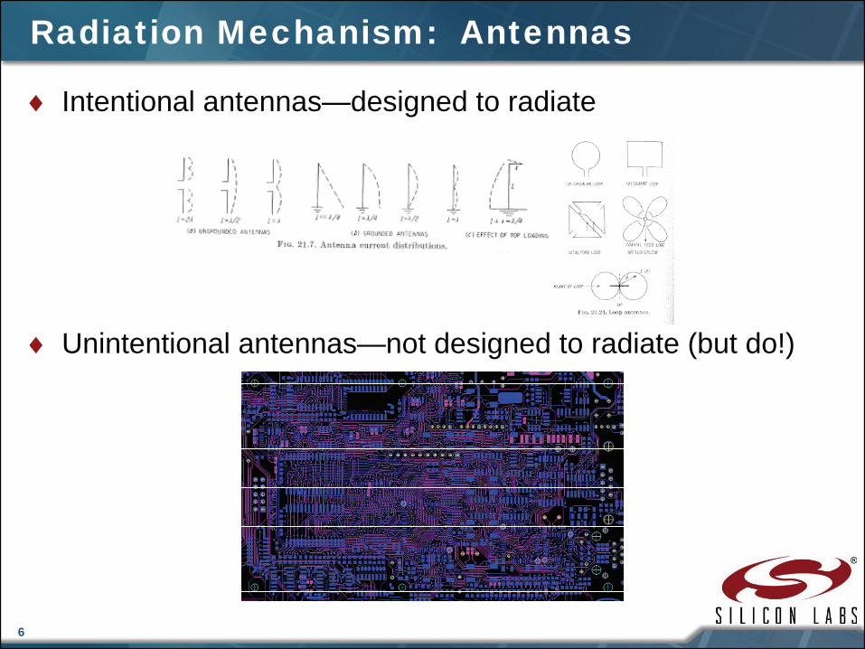
Radiation Mechanism: Antennas
♦ Intentional antennas—designed to radiate
♦ Unintentional antennas—not designed to radiate (but do!)
7
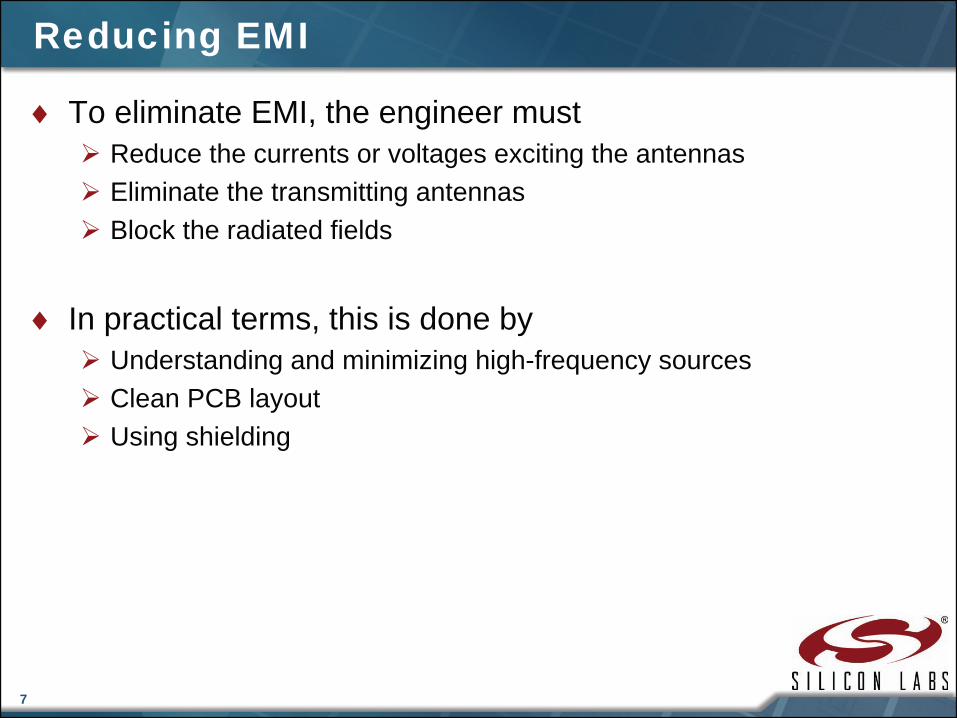
Reducing EMI
♦ To eliminate EMI, the engineer mustReduce the currents or voltages exciting the antennasEliminate the transmitting antennasBlock the radiated fields
♦ In practical terms, this is done byUnderstanding and minimizing high-frequency sourcesClean PCB layoutUsing shielding

8
Agenda
♦ EMI backgroundMechanisms Circuit-level causesFrequenciesMeasurementsShielding
♦ Example problem

9
What is the Source of EMI?
♦ CMOS digital devices are made of thousands of gates
♦ For simplicity, consider each gate as a CMOS inverter:
0
Vdd
0
Vdd

10
VDD Current
♦ In dynamic operation, transitions consume currentiCB: Crowbar current
Both gates are momentarily on at the same time, conducting current from Vdd to ground
iL: Load currentOutput of the gate is likely connected to input of another gateGate inputs are capacitive
Vddi
iCB iL
Vddi
iCB iL
11
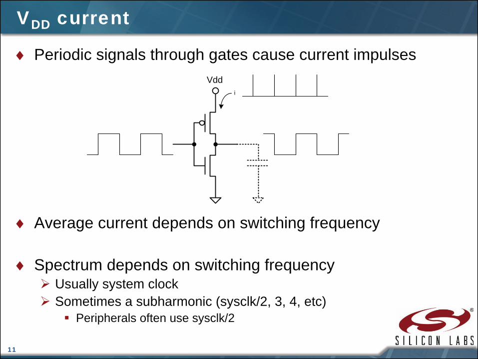
VDD current
♦ Periodic signals through gates cause current impulses
♦ Average current depends on switching frequency
♦ Spectrum depends on switching frequencyUsually system clock Sometimes a subharmonic (sysclk/2, 3, 4, etc)
Peripherals often use sysclk/2
Vddi

12
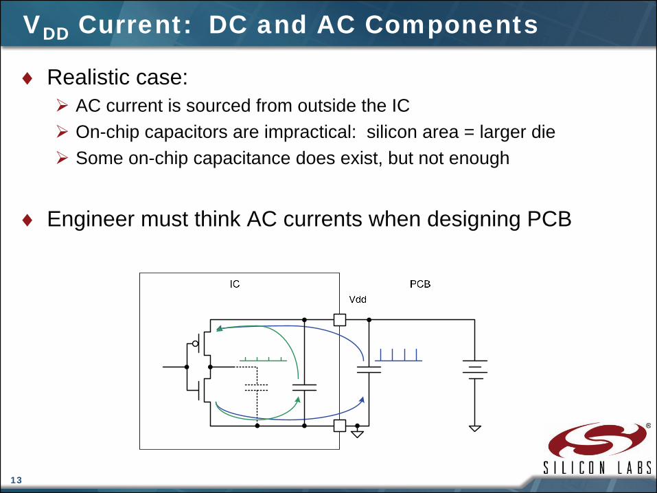
VDD Current: DC and AC Components
♦ Think in terms of both AC and DC power suppliesWhere does the AC current come from?
♦ Ideal caseMost AC current comes from on-chip sourcesLittle or no AC current comes from off-chip sourcesSmall current loop, small antenna
13
♦ Realistic case:AC current is sourced from outside the ICOn-chip capacitors are impractical: silicon area = larger dieSome on-chip capacitance does exist, but not enough
♦ Engineer must think AC currents when designing PCB
VDD Current: DC and AC Components
14
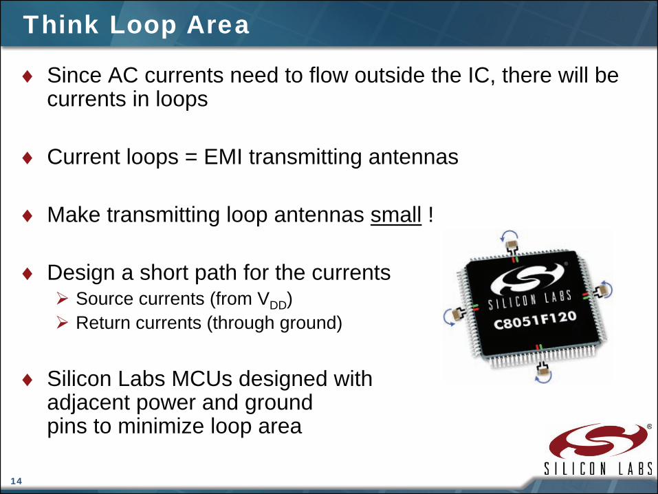
Think Loop Area
♦ Since AC currents need to flow outside the IC, there will be currents in loops
♦ Current loops = EMI transmitting antennas
♦ Make transmitting loop antennas small !
♦ Design a short path for the currentsSource currents (from VDD)Return currents (through ground)
♦ Silicon Labs MCUs designed with adjacent power and ground pins to minimize loop area
15
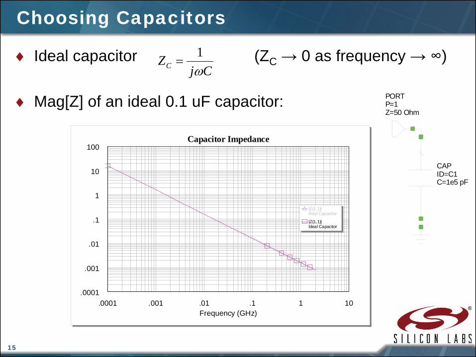
Choosing Capacitors
♦ Ideal capacitor (ZC → 0 as frequency → ∞)
♦ Mag[Z] of an ideal 0.1 uF capacitor:
CjZC ω
1=
.0001 .001 .01 .1 1 10Frequency (GHz)
Capacitor Impedance
.0001
.001
.01
.1
1
10
100
|Z(1,1)|Real Capacitor
|Z(1,1)|Ideal Capacitor
CAPID=C1C=1e5 pF
PORTP=1Z=50 Ohm

16
Choosing Capacitors
♦ Unfortunately there are no ideal capacitors♦ Real capacitor: capacitor in series with parasitic inductor♦ Inductor adds impedance with increasing frequency
.0001 .001 .01 .1 1 10Frequency (GHz)
Parasitic inductance
.0001
.01
1
100
|Z(1,1)|parasitic inductor
CAPID=C1C=1e5 pF
INDID=L1L=0.61 nH
PORTP=1Z=50 Ohm
LjCj
ZC ωω
+=1

17
Choosing Capacitors
♦ Real capacitor—inductance cancels, dominates impedance
♦ A capacitor behaves differently in three frequency bands1. f < SRF: Capacitor acts like a capacitor (Z ↓ as f ↑)2. f = SRF: Reactive impedances cancel3. f > SRF: Capacitor behaves like an inductor (Z ↑ as f ↑)
CAPID=C1C=1e5 pF
INDID=L1L=0.61 nH
PORTP=1Z=50 Ohm
LjCjZC ω
ω+
−=
.0001 .001 .01 .1 1 10Frequency (GHz)
Capacitor Impedance
.0001
.001
.01
.1
1
10
100
|Z(1,1)|Real Capacitor
|Z(1,1)|Ideal Capacitor
0.1uFSRF = 20MHz

18
Choosing Capacitors
♦ Wrong capacitor may have little or no effectCapacitors are capacitors only below SRFCapacitors are inductors above SRFIncreasing inductive impedance will prevent capacitor from sourcing impulse currents
VddIC PCB

19
Choosing Capacitors
♦ Solution: select another capacitorDifferent capacitor values have different parasiticsChoose capacitor for frequency of interest
♦ Help available from capacitor manufacturersMurata tool: http://www.murata.com/designlib/mcsil/index.html
20
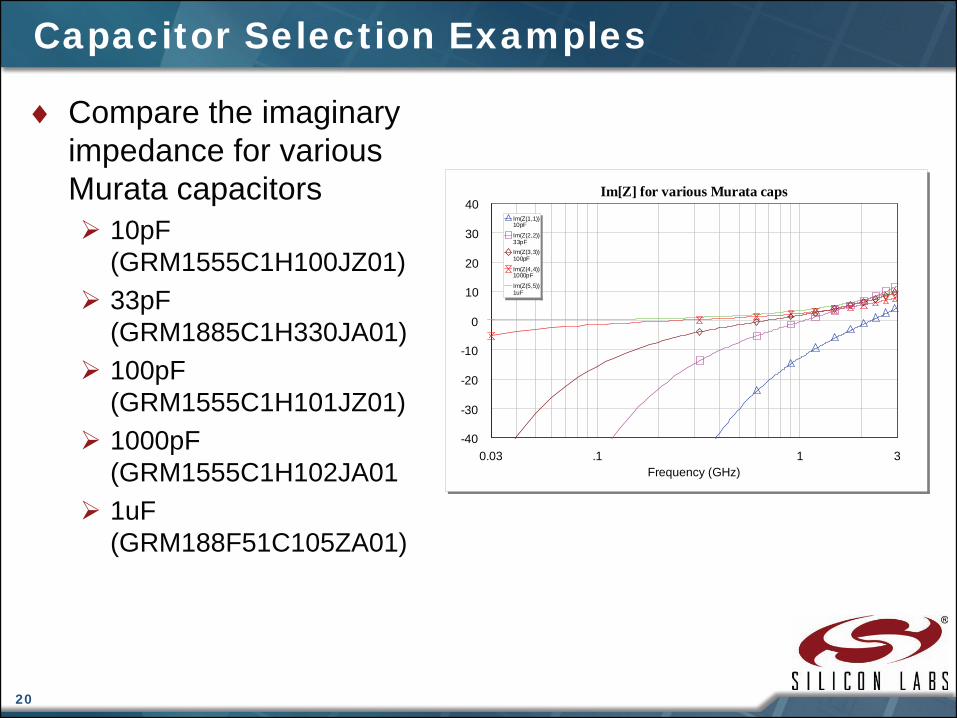
Capacitor Selection Examples
♦ Compare the imaginary impedance for various Murata capacitors
10pF (GRM1555C1H100JZ01)33pF(GRM1885C1H330JA01)100pF(GRM1555C1H101JZ01)1000pF(GRM1555C1H102JA011uF(GRM188F51C105ZA01)
0.03 3.1 1Frequency (GHz)
Im[Z] for various Murata caps
-40
-30
-20
-10
0
10
20
30
40Im(Z(1,1))10pF
Im(Z(2,2))33pFIm(Z(3,3))100pF
Im(Z(4,4))1000pF
Im(Z(5,5))1uF

21
Which Capacitor is Best?
♦ Use multiple capacitors in parallelExample: 10pF || 1000pF || 1uF
0.03 3.1 1Frequency (GHz)
parallel caps
-40
-30
-20
-10
0
10
20
30
40|Z(1,1)|parallel_caps
Im(Z(1,1))parallel_caps
22
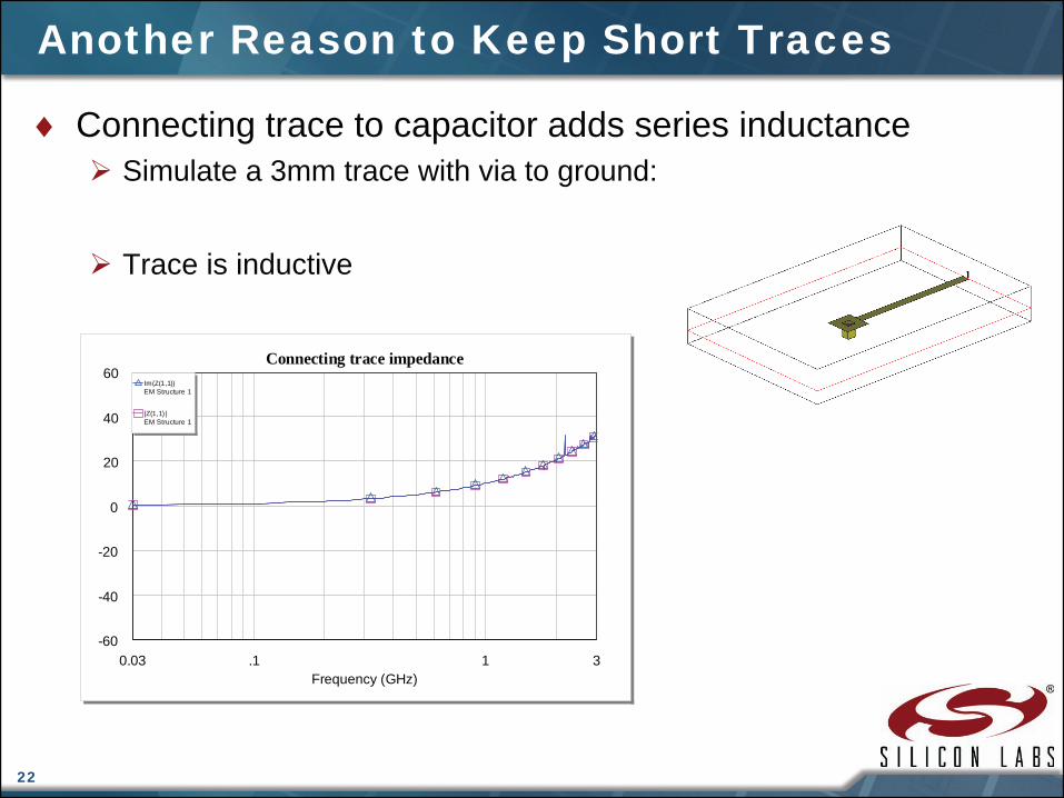
Another Reason to Keep Short Traces
♦ Connecting trace to capacitor adds series inductanceSimulate a 3mm trace with via to ground:
Trace is inductive
0.03 3.1 1Frequency (GHz)
Connecting trace impedance
-60
-40
-20
0
20
40
60Im(Z(1,1))EM Structure 1
|Z(1,1)|EM Structure 1

23
Parallel Caps in Series with Trace
♦ Parallel capacitor combination effectiveness is reduced by additional trace inductance
0.03 3.1 1Frequency (GHz)
parallel caps
-40
-30
-20
-10
0
10
20
30
40|Z(1,1)|parallel_caps
Im(Z(1,1))parallel_caps

24
Internal Coupling/Leakage
♦ EMI can result from AC energy coupling to digital I/O lines inside the IC
♦ Static digital I/O's may be a source of EMI♦ Possible causes:
Conduction through power supplyCapacitive couplingInductive coupling
VddIC PCB
25
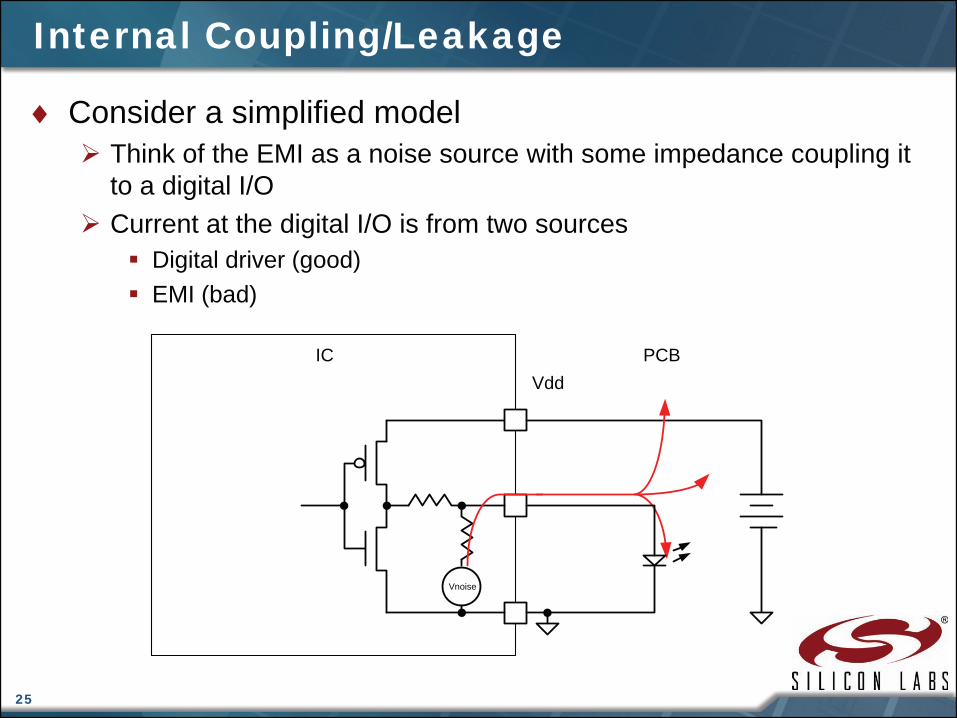
Internal Coupling/Leakage
♦ Consider a simplified modelThink of the EMI as a noise source with some impedance coupling it to a digital I/OCurrent at the digital I/O is from two sources
Digital driver (good)EMI (bad)
VddIC PCB
Vnoise
26
Internal Coupling/Leakage
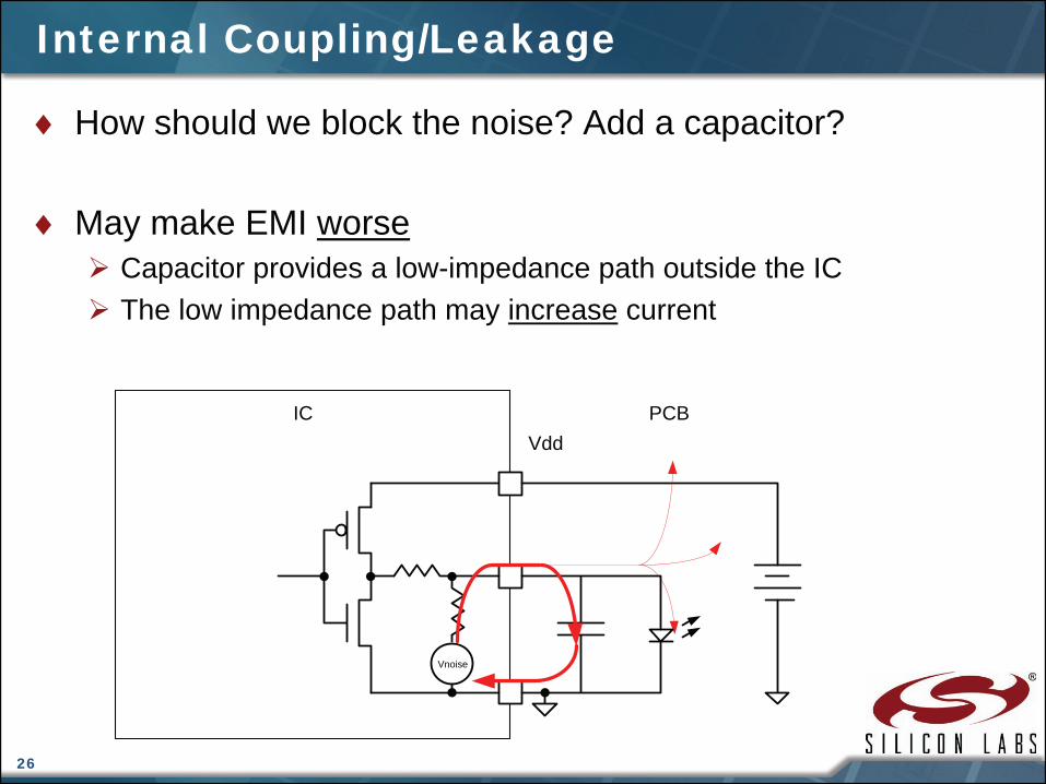
♦ How should we block the noise? Add a capacitor?
♦ May make EMI worseCapacitor provides a low-impedance path outside the ICThe low impedance path may increase current
VddIC PCB
Vnoise
27
Internal Coupling/Leakage
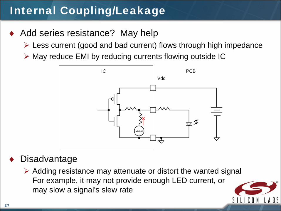
♦ Add series resistance? May helpLess current (good and bad current) flows through high impedanceMay reduce EMI by reducing currents flowing outside IC
♦ DisadvantageAdding resistance may attenuate or distort the wanted signalFor example, it may not provide enough LED current, or may slow a signal's slew rate
VddIC PCB
Vnoise
28
Internal Coupling/Leakage
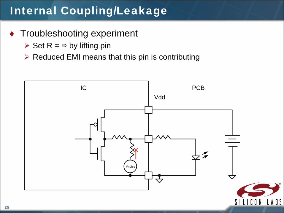
♦ Troubleshooting experimentSet R = ∞ by lifting pinReduced EMI means that this pin is contributing
VddIC PCB
Vnoise

29
Internal Coupling/Leakage
♦ Add an external inductor or choke?Provides high impedance for high frequencies, low impedance for low frequencies
♦ DisadvantagesInductor may actually create and radiate EMI (inductors turn electric currents into magnetic fields)Inductors cost more than resistors and capacitors
VddIC PCB
Vnoise

30
Agenda
♦ EMI backgroundMechanisms Circuit-level causesFrequenciesMeasurementsShielding
♦ Example problem

31
Time and Frequency Domains
♦ Signals can be represented in time or frequency domainsFourier transform F: Transform between time and frequency domainsDigital designers think in time domainEMI measurements are in the frequency domain
♦ Periodic events in a circuit create distinct EMI frequenciesFrequencies often harmonics of the system clockFrequencies may be harmonics of system clock subharmonics
Example: Flash memory read every third sysclock periodDigital waveforms will create harmonics
Square wave creates odd harmonicsImpulse train creates even and odd harmonics

32
Fourier Transform Review
♦ Square waveSquare wave is composed of several odd harmonics

33
Fourier Transform Review
♦ Impulse trainA series of pulses in time is a series of tones in frequency

34
Example—Spectrum of a Square Wave
♦ F120 24.5MHz sysclock from a port pin
A
* RBW 500 kHz
VBW 2 MHz
SWT 2.5 msRef 10 dBm Att 35 dB
Start 10 MHz Stop 200 MHz19 MHz/
EXT
1 SAAVG
-90
-80
-70
-60
-50
-40
-30
-20
-10
0
10
SWP 100 of 100
Date: 23.MAY.2007 10:11:54
Oscilloscope (time) Spectrum Analyzer (frequency)

35
A
* RBW 500 kHz
VBW 2 MHz
SWT 2.5 msRef 10 dBm Att 35 dB
Start 10 MHz Stop 200 MHz19 MHz/
EXT
1 SAAVG
-90
-80
-70
-60
-50
-40
-30
-20
-10
0
10
SWP 100 of 100
Date: 23.MAY.2007 10:11:54
System Clock Design Tradeoffs
♦ Difficult to change waveform
♦ Easy to change system clock
Example—C8051F120reduce sysclk using clock dividersincrease sysclk using clock multiplier24.5MHz shown here

36
Spectrum of 3.0625 MHz System Clock
A
* RBW 500 kHz
VBW 2 MHz
SWT 2.5 msRef 10 dBm Att 35 dB
Start 10 MHz Stop 200 MHz19 MHz/
EXT
AVG1 SA
-90
-80
-70
-60
-50
-40
-30
-20
-10
0
10
SWP 100 of 100
Date: 23.MAY.2007 10:09:28
37
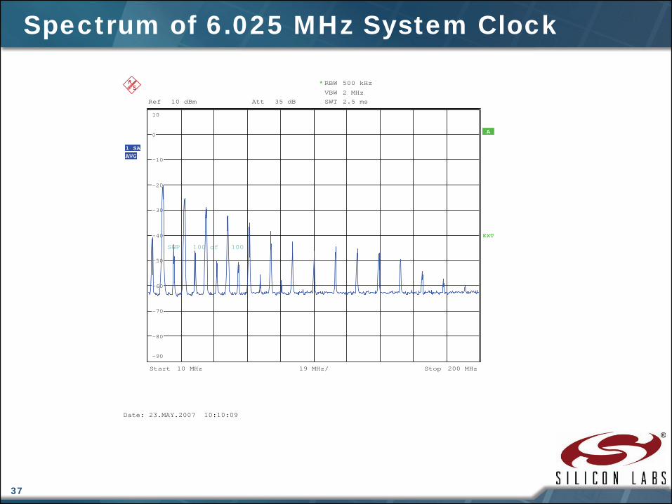
Spectrum of 6.025 MHz System Clock
A
* RBW 500 kHz
VBW 2 MHz
SWT 2.5 msRef 10 dBm Att 35 dB
Start 10 MHz Stop 200 MHz19 MHz/
EXT
1 SAAVG
-90
-80
-70
-60
-50
-40
-30
-20
-10
0
10
SWP 100 of 100
Date: 23.MAY.2007 10:10:09

38
Spectrum of 12.25 MHz System Clock
A
* RBW 500 kHz
VBW 2 MHz
SWT 2.5 msRef 10 dBm Att 35 dB
Start 10 MHz Stop 200 MHz19 MHz/
EXT
1 SAAVG
-90
-80
-70
-60
-50
-40
-30
-20
-10
0
10
SWP 100 of 100
Date: 23.MAY.2007 10:10:44

39
Spectrum of 24.5 MHz System Clock
A
* RBW 500 kHz
VBW 2 MHz
SWT 2.5 msRef 10 dBm Att 35 dB
Start 10 MHz Stop 200 MHz19 MHz/
EXT
1 SAAVG
-90
-80
-70
-60
-50
-40
-30
-20
-10
0
10
SWP 100 of 100
Date: 23.MAY.2007 10:11:54

40
Spectrum of 49 MHz System Clock
A
* RBW 500 kHz
VBW 2 MHz
SWT 2.5 msRef 10 dBm Att 35 dB
Start 10 MHz Stop 200 MHz19 MHz/
EXT
1 SAAVG
-90
-80
-70
-60
-50
-40
-30
-20
-10
0
10
SWP 100 of 100
Date: 23.MAY.2007 10:14:42

41
Spectrum of 98 MHz System Clock
A
* RBW 500 kHz
VBW 2 MHz
SWT 2.5 msRef 10 dBm Att 35 dB
Start 10 MHz Stop 200 MHz19 MHz/
EXT
1 SAAVG
-90
-80
-70
-60
-50
-40
-30
-20
-10
0
10
SWP 100 of 100
Date: 23.MAY.2007 10:14:02

42
Agenda
♦ EMI backgroundMechanisms Circuit-level causesFrequenciesMeasurementsShielding
♦ Example problem

43
Measuring EMI
♦ Measured by an accredited EMI test facility
Open-Air Test Site (OATS)
Device placed 3 or 10 meters from measurement antennaQuiet, reflection-free environmentOutdoors or anechoic chamber

44
Measuring EMI—Accredited Test Facility
♦ OATS test resultsListed in a tableIncludes all frequencies foundShows both passing/failing frequenciesData for horizontal and vertical receiving antenna polarization
45
Measuring EMI
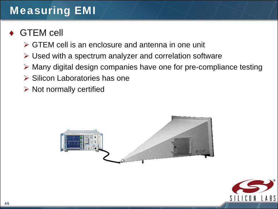
♦ GTEM cellGTEM cell is an enclosure and antenna in one unitUsed with a spectrum analyzer and correlation softwareMany digital design companies have one for pre-compliance testingSilicon Laboratories has oneNot normally certified

46
Measuring EMI—GTEM
♦ GTEM test resultsContinuous test data vs. tabularMeasurement shows computed OATS equivalentData shows worst-case antenna orientation
OATS Equivalent Radiated Emissions
-20.00
-10.00
0.00
10.00
20.00
30.00
40.00
50.00
60.00
1.000E+01 1.000E+02 1.000E+03
f(MHz)
dBuV
/m OATS 10m (dBuV/m)CISPR-22 QPk Cl B Limits

47
Measuring EMI
♦ Loop antennaSimple and inexpensiveCan make one yourselfUsed with a spectrum analyzerGood only for relative measurements
48
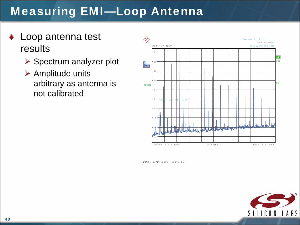
Measuring EMI—Loop Antenna
♦ Loop antenna test results
Spectrum analyzer plotAmplitude units arbitrary as antenna is not calibrated
A
PASPUEM
Ref 27 dBµV
SGL1MAXH
Center 1.515 GHz Span 2.97 GHz297 MHz/
-20
-15
-10
-5
0
5
10
15
20
25
SWP 100 of 100
1
Marker 1 [T1 ]
-19.86 dBµV
43.662000000 MHz
Date: 3.APR.2007 13:47:56

49
Agenda
♦ EMI backgroundMechanisms Circuit-level causesFrequenciesMeasurementsShielding
♦ Example problem

50
Shielding—Theory
♦ Faraday cageMade of conductive materialCharges in conductor move to cancel electric fieldFaraday cage can keep fields out or in

51
Shielding—Troubleshooting
♦ Copper Foil TapeAvailable from 3M(www.3m.com, search for '1125')
♦ Tips and TricksMake good ground connection
Leave no gapsSolder to ground in many places
Start by shielding small areasShield a device or specific traces rather than a large area: helps pinpoint EMI source
Adhesive is not conductive(Even if manufacturer says it is)Use solder for good connection
Use Kapton tape beneath copperKeeps copper tape from shorting out IC pins

52
Shielding—Production PCB
♦ Production: ShieldsCommonly used in wireless, computational productsEffective, but adds costGood source for off-the-shelf shields: Leader-Tech (www.leadertechinc.com)

53
Shielding—Troubleshooting
♦ Conductive paintUse to convert non-conductive plastic enclosures to conductive, EMI-shielded enclosuresUse in troubleshooting or productionConductive plastics commonly used in laptop PC's, mobile phones, PDA's, etcAvailable from MG chemicals:(http://www.mgchemicals.com/products/shielding.html)

54
Agenda
♦ EMI backgroundMechanisms Circuit-level causesFrequenciesMeasurementsShielding
♦ Example problem

55
Example Problem
♦ Product is a GPS data logger using a C8051F120 MCU♦ Problem—GPS receiver sometimes loses satellite reception
♦ HypothesisEMI may be radiating from the micro in to the GPS antennaEMI may be conducted from the micro to the power supplyor control lines of the GPS
MCU
GPS
LDO
56
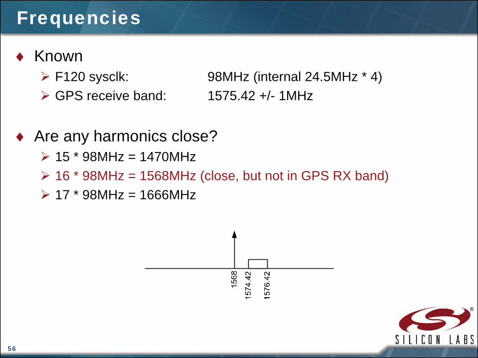
Frequencies
♦ KnownF120 sysclk: 98MHz (internal 24.5MHz * 4)GPS receive band: 1575.42 +/- 1MHz
♦ Are any harmonics close?15 * 98MHz = 1470MHz16 * 98MHz = 1568MHz (close, but not in GPS RX band)17 * 98MHz = 1666MHz

57
Frequencies
♦ Nominal casesysclk = 24.5 * 4
♦ From datasheetsysclk = (24.5 ± 2%) * 4
♦ Revisiting 16th harmonic16 * (24.0 * 4) = 1536MHz16 * (25.0 * 4) = 1600MHz
♦ Conclusion16th harmonic can interfere with GPS reception
1574
.42
1576
.42
1568
1536
1600
58
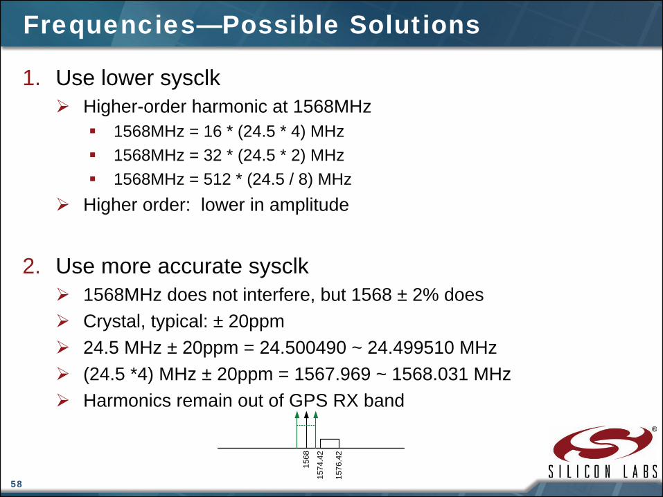
Frequencies—Possible Solutions
1. Use lower sysclkHigher-order harmonic at 1568MHz
1568MHz = 16 * (24.5 * 4) MHz1568MHz = 32 * (24.5 * 2) MHz1568MHz = 512 * (24.5 / 8) MHz
Higher order: lower in amplitude
2. Use more accurate sysclk1568MHz does not interfere, but 1568 ± 2% doesCrystal, typical: ± 20ppm24.5 MHz ± 20ppm = 24.500490 ~ 24.499510 MHz(24.5 *4) MHz ± 20ppm = 1567.969 ~ 1568.031 MHzHarmonics remain out of GPS RX band
1574
.42
1576
.42
1568

59
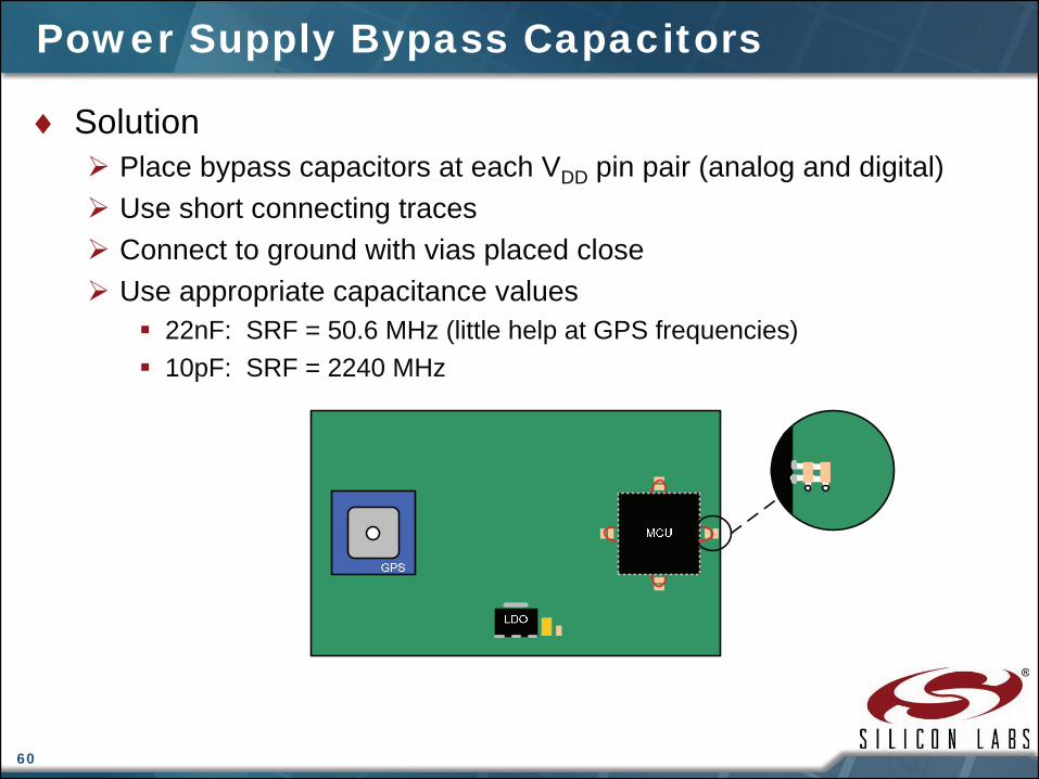
Power Supply Bypass Capacitors
♦ Insufficient power supply bypassingC8051F120 has four power supply/ground pin pairs: each should have capacitorsLack of local capacitors may cause larger current loopsSingle value of capacitor may not be effective for all frequencies
MCU
GPS
LDO
60
Power Supply Bypass Capacitors
♦ SolutionPlace bypass capacitors at each VDD pin pair (analog and digital)Use short connecting tracesConnect to ground with vias placed closeUse appropriate capacitance values
22nF: SRF = 50.6 MHz (little help at GPS frequencies)10pF: SRF = 2240 MHz

61
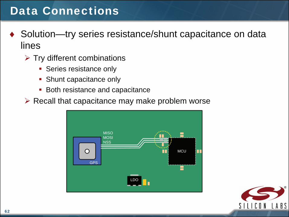
Data Connections
♦ EMI may conduct through data lines between MCU and GPS
MCU
GPS
LDO
MISOMOSINSS
62
Data Connections
♦ Solution—try series resistance/shunt capacitance on data lines
Try different combinationsSeries resistance onlyShunt capacitance onlyBoth resistance and capacitance
Recall that capacitance may make problem worse
MCU
GPS
LDO
MISOMOSINSS
63
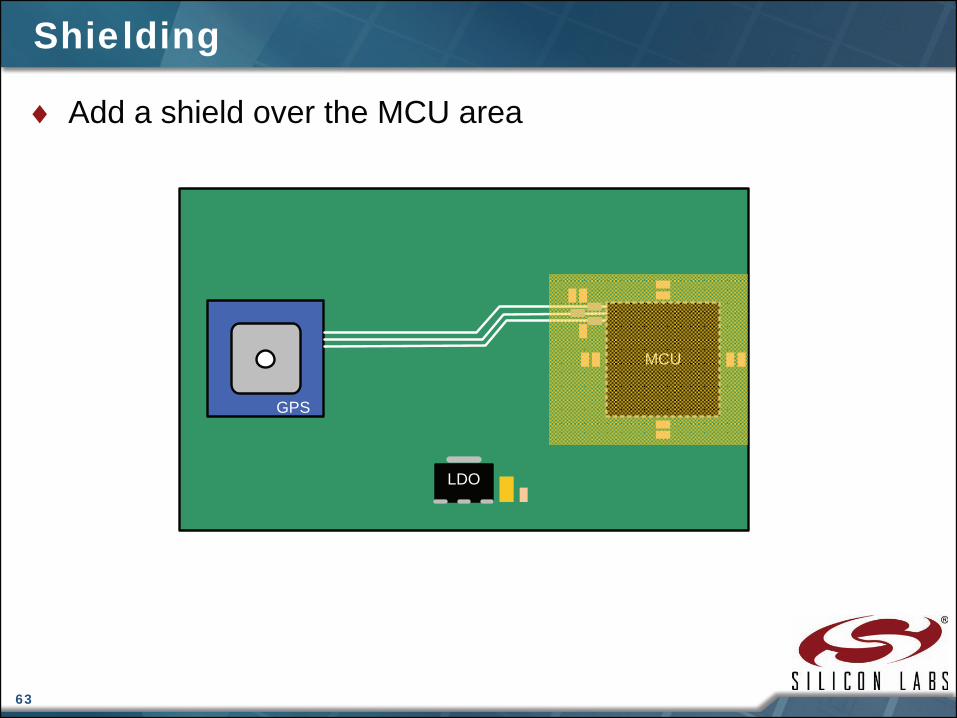
Shielding
♦ Add a shield over the MCU area
MCU
GPS
LDO

64
Shielding
♦ Use ground plane as shieldMount MCU and GPS on opposite sides of PCB

65
Summary
♦ To effectively understand EMI problemsUnderstand the frequencies involved and their relation to the system clockExpect high frequency harmonicsConsider every node and trace as a potential radiating antenna
♦ To effectively troubleshoot EMI problemsThink about minimizing the power supply path for high frequenciesSelect the correct capacitorsDesign the PCB to minimize loop areasFilter signal linesUse shielding if necessary
♦ There is no single EMI fix for all problemsDon't be afraid to experiment!

www.silabs.com/MCU


