Journal of Electrical Engineering & T echnology, V ol. 1, No. 4, pp. 503~512, 2006 503Unified Power Quality Conditioner for Compensating Voltage Interruption Byung-Moon Han † , Bo-Hyung Cho*, Seung-Ki Sul* and Jae-Eon Kim** Abstract - This paper proposes a new configuration for the Unified Power Quality Conditioner, which has a DC/DC converter with super-capacitors for energy storage. The proposed UPQC can compensate the reactive power, harmonic current, voltage sag and swell, voltage imbalance, and voltage interruption. The performance of the proposed system was analyzed through simulations with PSCAD/EMTDC software. The feasibility of system implementation is confirmed through experi- mental works with a prototype. The proposed UPQC has ultimate capability to improve the power quality at the point of installation on power distribution systems and industrial power systems. Keywords:DC/DC Converter, PSCAD/EMTDC (Power System Computer Aided Design/Electro Magnetic Transients DC analysis program), Super-capacitor bank, UPQC (Unified Power Quality Conditioner), Voltage interruption 1. Introduction As more sensitive loads, such as computers, automation equipments, communication equipments, medical equip- ments, and military equipments, have come into wide use, power quality has become a significant issue to both customers and the utility companies. Since these equipments are very sensitive in relation to input voltage disturbances, the inadequate operation or the fault of these loads brings about huge losses [1-3]. The elimination or mitigation of disturbances propagated from the distribution system is absolutely required to improve the operational reliability of these loads. The terminology and the guidelines for power quality has been described in detail at IEEE-519 and IEC-555 [4]. According to these guidelines, the voltage sag or swell is allowed by 10%, the total harmonic distortion is allowed by 5%, and the voltage unbalance is a llowed by 10% [5]. UPQC has been widely studied in order to improve universal power quality by many researchers [6-8]. The function of UPQC is to mitigate the disturbance that affects the performance of the critical load. The UPQC, which has two inverters that share one dc link capacitor, can compensate the voltage sag and swell, the harmonic current and voltage, and control the power flow and voltage stability. However, the UPQC cannot compensate for the voltage interruption because it has no energy storage in the dc link. This paper proposes a new configuration for the UPQC that consists of a DC/DC converter and super-capacitors for energy storage. The operation of the proposed system was verified through simulations with PSCAD/EMTDC software, and the feasibility of hardware implementation was confirmed through experimental works with a prototype of 20kV A rating. 2. Configuration of proposed UPQC The UPQC is utilized for simultaneous compensation of the load current and the voltage disturbance at the source side. Normally the UPQC has two voltage-source inverters of three-phase four-wire or three-phase three-wire confi- guration. One inverter, called the series inverter is connected through transformers between the source and the common connection point. The other inverter, called the shunt inverter is connected in parallel through the transformers. The series inverter operates as a voltage source, while the shunt inverter operates as a current source. The UPQC has compensation capabilities for the harmonic current, the reactive power compensation, the voltage disturbances, and the power flow control. However , it has no compensation capability for voltage interruption because no energy is stored. This paper proposes a new configuration for the UPQC that has the super-capacitors for energy storage connected to the dc link through the DC/DC converter. The proposed UPQC can compensate the voltage interruption in the †Corresponding Author: Dep t. of Electri cal Engineering , Myongj i University , Korea. ( erichan@mju .ac.kr) * School of Electrical Engineering and Com puter Science, Seoul National University , Korea. (bhcho@snu .ac.kr), ([email protected]) ** School of Electrical & Computer Eng ineering, Chungbu k National University , Korea. ([email protected]) Received October 24, 2005 ; Accepted June 5, 2006
Transcript
8/10/2019 Unified Power Quality Conditioner for Compensating Voltage Interruption
Journal of Electrical Engineering & Technology, Vol. 1, No. 4, pp. 503~512, 2006 503
Unified Power Quality Conditionerfor Compensating Voltage Interruption
Byung-Moon Han † , Bo-Hyung Cho*, Seung-Ki Sul* and Jae-Eon Kim**
Abstract - This paper proposes a new configuration for the Unified Power Quality Conditioner,which has a DC/DC converter with super-capacitors for energy storage. The proposed UPQC cancompensate the reactive power, harmonic current, voltage sag and swell, voltage imbalance, andvoltage interruption. The performance of the proposed system was analyzed through simulations withPSCAD/EMTDC software. The feasibility of system implementation is confirmed through experi-mental works with a prototype. The proposed UPQC has ultimate capability to improve the powerquality at the point of installation on power distribution systems and industrial power systems.
Keywords : DC/DC Converter, PSCAD/EMTDC (Power System Computer Aided Design/ElectroMagnetic Transients DC analysis program), Super-capacitor bank, UPQC (Unified Power QualityConditioner), Voltage interruption
1. Introduction
As more sensitive loads, such as computers, automationequipments, communication equipments, medical equip-ments, and military equipments, have come into wide use,
power quality has become a significant issue to bothcustomers and the utility companies. Since theseequipments are very sensitive in relation to input voltagedisturbances, the inadequate operation or the fault of theseloads brings about huge losses [1-3]. The elimination ormitigation of disturbances propagated from the distributionsystem is absolutely required to improve the operationalreliability of these loads.
The terminology and the guidelines for power qualityhas been described in detail at IEEE-519 and IEC-555 [4].According to these guidelines, the voltage sag or swell isallowed by 10%, the total harmonic distortion is allowed
by 5%, and the voltage unbalance is allowed by 10% [5].UPQC has been widely studied in order to improveuniversal power quality by many researchers [6-8]. Thefunction of UPQC is to mitigate the disturbance that affectsthe performance of the critical load. The UPQC, which hastwo inverters that share one dc link capacitor, cancompensate the voltage sag and swell, the harmonic currentand voltage, and control the power flow and voltagestability. However, the UPQC cannot compensate for the
voltage interruption because it has no energy storage in thedc link.
This paper proposes a new configuration for the UPQCthat consists of a DC/DC converter and super-capacitorsfor energy storage. The operation of the proposed systemwas verified through simulations with PSCAD/EMTDCsoftware, and the feasibility of hardware implementationwas confirmed through experimental works with a
prototype of 20kVA rating.
2. Configuration of proposed UPQC
The UPQC is utilized for simultaneous compensation ofthe load current and the voltage disturbance at the sourceside. Normally the UPQC has two voltage-source invertersof three-phase four-wire or three-phase three-wire confi-guration. One inverter, called the series inverter isconnected through transformers between the source and thecommon connection point. The other inverter, called theshunt inverter is connected in parallel through thetransformers. The series inverter operates as a voltagesource, while the shunt inverter operates as a currentsource.
The UPQC has compensation capabilities for theharmonic current, the reactive power compensation, thevoltage disturbances, and the power flow control. However,it has no compensation capability for voltage interruption
because no energy is stored.This paper proposes a new configuration for the UPQC
that has the super-capacitors for energy storage connectedto the dc link through the DC/DC converter. The proposedUPQC can compensate the voltage interruption in the
† Corresponding Author: Dept. of Electrical Engineering, MyongjiUniversity, Korea. ([email protected])
* School of Electrical Engineering and Computer Science, Seoul
Byung-Moon Han, Bo-Hyung Cho, Seung-Ki Sul and Jae-Eon Kim 505
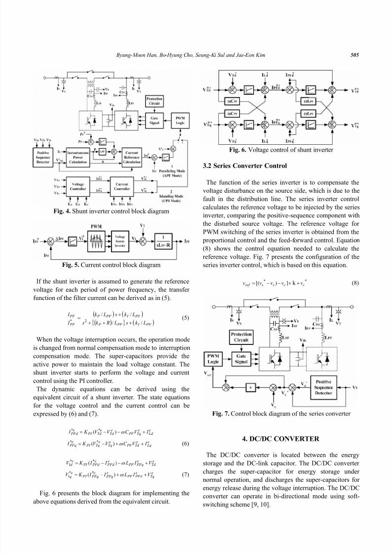
Fig. 4. Shunt inverter control block diagram
Fig. 5. Current control block diagram
If the shunt inverter is assumed to generate the reference
voltage for each period of power frequency, the transferfunction of the filter current can be derived as in (5).
( ) ( )( ){ } ( ) PF I PF P
PF I PF P
PF
PF
Lk s L Rk s
Lk s Lk
I
I
//
//2* +++
+= (5)
When the voltage interruption occurs, the operation modeis changed from normal compensation mode to interruptioncompensation mode. The super-capacitors provide theactive power to maintain the load voltage constant. Theshunt inverter starts to perform the voltage and currentcontrol using the PI controller.
The dynamic equations can be derived using theequivalent circuit of a shunt inverter. The state equationsfor the voltage control and the current control can beexpressed by (6) and (7).
e Ld
eTq PF
eTd
eTd PI
e PFd I V C V V K I +−−= ω )( **
e Lq
eTd PF
eTq
eTq PI
e PFq I V C V V K I ++−= ω )( ** (6)
eTd
e PFq PF
e PFd
e PFd PI
ed V I L I I K V +−−= ω )( **
1
eTq
e PFd PF
e PFq
e PFq PI
eq V I L I I K V ++−= ω )( **
1 (7)
Fig. 6 presents the block diagram for implementing theabove equations derived from the equivalent circuit.
Fig. 6. Voltage control of shunt inverter
3.2 Series Converter Control
The function of the series inverter is to compensate thevoltage disturbance on the source side, which is due to thefault in the distribution line. The series inverter controlcalculates the reference voltage to be injected by the seriesinverter, comparing the positive-sequence component withthe disturbed source voltage. The reference voltage forPWM switching of the series inverter is obtained from the
proportional control and the feed-forward control. Equation(8) shows the control equation needed to calculate thereference voltage. Fig. 7 presents the configuration of theseries inverter control, which is based on this equation.
×−−= ])[( *c s sref vvvv k *
cv+ (8)
Fig. 7. Control block diagram of the series converter
4. DC/DC CONVERTER
The DC/DC converter is located between the energystorage and the DC-link capacitor. The DC/DC convertercharges the super-capacitor for energy storage undernormal operation, and discharges the super-capacitors forenergy release during the voltage interruption. The DC/DCconverter can operate in bi-directional mode using soft-switching scheme [9, 10].
8/10/2019 Unified Power Quality Conditioner for Compensating Voltage Interruption
506 Unified Power Quality Conditioner for Compensating Voltage Interruption
4.1. Energy Storage Design
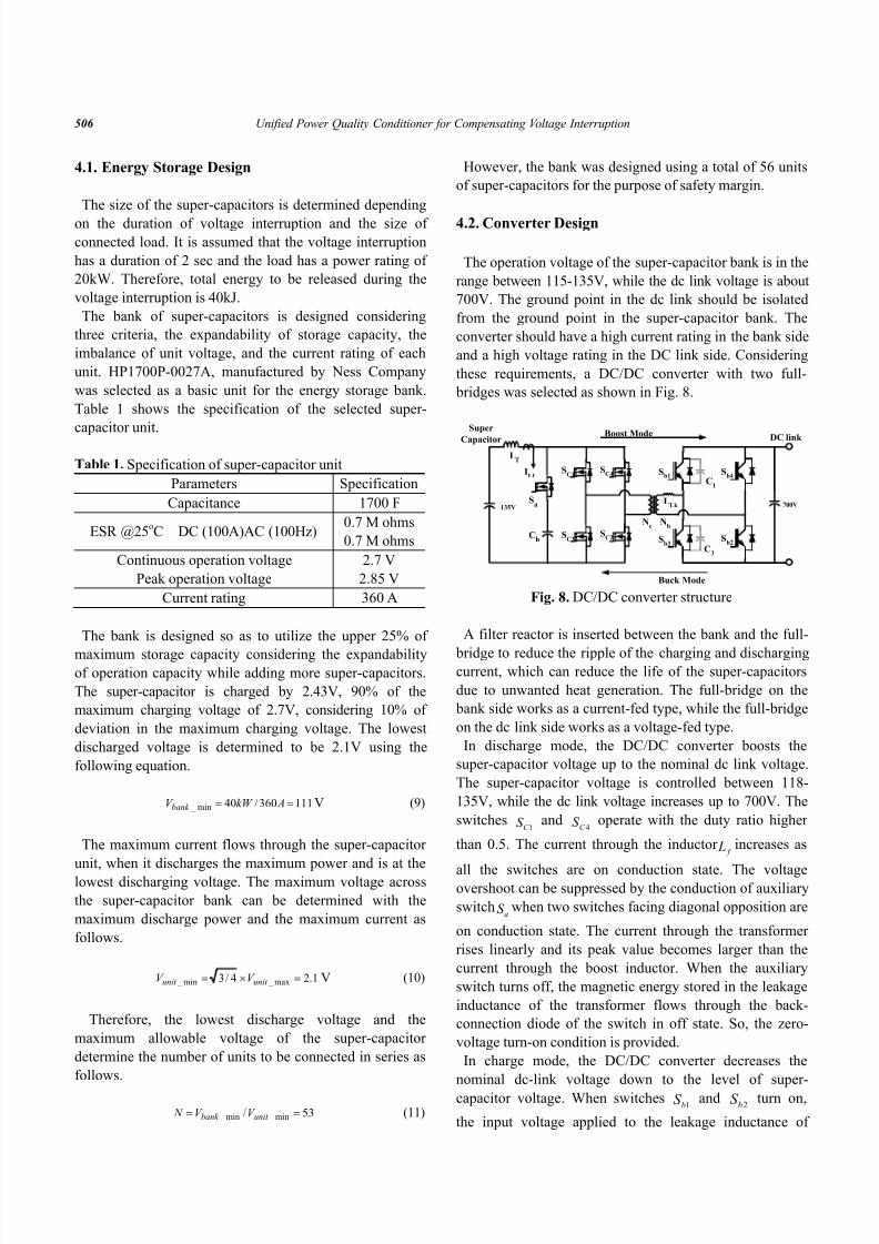
The size of the super-capacitors is determined dependingon the duration of voltage interruption and the size ofconnected load. It is assumed that the voltage interruptionhas a duration of 2 sec and the load has a power rating of20kW. Therefore, total energy to be released during thevoltage interruption is 40kJ.
The bank of super-capacitors is designed consideringthree criteria, the expandability of storage capacity, theimbalance of unit voltage, and the current rating of eachunit. HP1700P-0027A, manufactured by Ness Companywas selected as a basic unit for the energy storage bank.Table 1 shows the specification of the selected super-capacitor unit.
Table 1. Specification of super-capacitor unitParameters SpecificationCapacitance 1700 F
ESR @25 oC DC (100A)AC (100Hz)0.7 M ohms0.7 M ohms
Continuous operation voltagePeak operation voltage
2.7 V2.85 V
Current rating 360 A
The bank is designed so as to utilize the upper 25% of
maximum storage capacity considering the expandabilityof operation capacity while adding more super-capacitors.The super-capacitor is charged by 2.43V, 90% of themaximum charging voltage of 2.7V, considering 10% ofdeviation in the maximum charging voltage. The lowestdischarged voltage is determined to be 2.1V using thefollowing equation.
111360/40min _ == AkW V bank V (9)
The maximum current flows through the super-capacitorunit, when it discharges the maximum power and is at thelowest discharging voltage. The maximum voltage acrossthe super-capacitor bank can be determined with themaximum discharge power and the maximum current asfollows.
1.24/3 max _ min _ =×= unit unit V V V (10)
Therefore, the lowest discharge voltage and themaximum allowable voltage of the super-capacitordetermine the number of units to be connected in series asfollows.
53/ min _ min _ == unit bank V V N (11)
However, the bank was designed using a total of 56 unitsof super-capacitors for the purpose of safety margin.
4.2. Converter Design
The operation voltage of the super-capacitor bank is in therange between 115-135V, while the dc link voltage is about700V. The ground point in the dc link should be isolatedfrom the ground point in the super-capacitor bank. Theconverter should have a high current rating in the bank sideand a high voltage rating in the DC link side. Consideringthese requirements, a DC/DC converter with two full-
bridges was selected as shown in Fig. 8.
L f
Sa
C h
SC1
SC3
SC4
SC2
Nc Nb
Sb1
Sb3
Sb4
Sb2
Boost Mode
Buck Mode
135V 700V
ILf
DC link Super
Capacitor
C 1
C 3
L Lk
Fig. 8. DC/DC converter structure
A filter reactor is inserted between the bank and the full-
bridge to reduce the ripple of the charging and dischargingcurrent, which can reduce the life of the super-capacitorsdue to unwanted heat generation. The full-bridge on the
bank side works as a current-fed type, while the full-bridgeon the dc link side works as a voltage-fed type.
In discharge mode, the DC/DC converter boosts thesuper-capacitor voltage up to the nominal dc link voltage.The super-capacitor voltage is controlled between 118-135V, while the dc link voltage increases up to 700V. Theswitches
1C S and4C S operate with the duty ratio higher
than 0.5. The current through the inductor f L increases as
all the switches are on conduction state. The voltageovershoot can be suppressed by the conduction of auxiliaryswitch
aS when two switches facing diagonal opposition are
on conduction state. The current through the transformerrises linearly and its peak value becomes larger than thecurrent through the boost inductor. When the auxiliaryswitch turns off, the magnetic energy stored in the leakageinductance of the transformer flows through the back-connection diode of the switch in off state. So, the zero-voltage turn-on condition is provided.
In charge mode, the DC/DC converter decreases thenominal dc-link voltage down to the level of super-capacitor voltage. When switches 1bS and 2bS turn on,
the input voltage applied to the leakage inductance of
8/10/2019 Unified Power Quality Conditioner for Compensating Voltage Interruption
Byung-Moon Han, Bo-Hyung Cho, Seung-Ki Sul and Jae-Eon Kim 507
transformer L Lk increases the input current. The power inthe primary side is transferred to the secondary side. Thesecondary voltage charges the capacitor C h through thereverse connected diode of auxiliary switch aS . If the
charging voltage is high enough to make the chargingcurrent zero, switch
1bS turns off. Switch 3bS turns off
with zero-voltage scheme while capacitor C 1 is chargedand capacitor C 3 is discharged. When auxiliary
aS turns
on, the voltage across the auxiliary capacitor affects the primary voltage of the coupling transformer. This voltageis applied to the leakage inductance L Lk with reverse
polarity. This makes the primary current zero and switch
2bS turns off with zero-current scheme.
InverterSuper
Capacitor
DC/DC Convertermodule # 1
PWM Ramp
diL-
+
DC/DC Convertermodule # 2
PWM Ramp
diSC-
+
DC/DC Convertermodule # 3
PWM Ramp
d-
+
DC/DC Convertermodule # 4
PWM Ramp
d- +
OSC
V ref
VC
iSC
iSC
Fig. 9. Four module parallel operation and PWM pulse
interleaving
From a design point of view it is not effective to build asingle 20kW DC/DC converter due to the restriction in
power rating of the switching unit. Since super-capacitorsoperate at low-voltage large-current, the switchingfrequency is limited by the critical value of di/dt, whichdepends on the leakage inductance of the couplingtransformer. So, when the converter is designed in a singlemodule, the switching ripple of charging or dischargingcurrent is high. Therefore, the proposed DC/DC converterhas four modules of a 5kW converter connected in parallelinstead of one module of a 20kW converter. When themulti-module is used, it is possible to expand the systemrating and to increase the operation reliability. Also, theswitching ripple of the charging or discharging current can
be sharply reduced using the interleaving scheme of PWMswitching.
4.3. Controller Design
The controller of the DC/DC converter is comprised ofthe main control, charging control, and discharging control.
One function of the main control is to select the chargemode and discharge mode according to the command fromthe UPQC main controller. The other function of the maincontrol is to monitor the operation of each convertermodule and to remove the module in fault. The maincontrol also monitors the maximum and minimum chargeor discharge voltage.
The discharge control was designed to charge the supercapacitors when the voltage interruption occurs in the acside. The charge operation is performed with four modulesin the 20kW power rating. The discharge control consistsof two control loops, which are the outer loop of voltagecontrol and the inner loop of current control as shown inFig. 10. The voltage control loop measures the DC linkvoltage and compares it with the reference voltage. Theerror passes through the RC circuit to calculate thereference current for the inner-loop current control. Theinner-loop current control measures the discharge currenton bank side and compares it with the reference currentobtained from the outer-loop voltage control. The error
passes through the RC circuit to calculate the duty ratio forthe DC/DC converter module.
+
_
V ref
VO
C
I ref
f pv
R f v Cf zv
R iv
(LM358) (a) Outer-Loop voltage control
+
_
I ref
C
R fc
k 1
I sense
f pc
Cf zcIL k
(LM358)
k 2 d
R ic
(b) Inner-Loop current control
Fig. 10. Discharge control structure
The charge control was designed to charge the supercapacitor in a slow speed in order to prevent any DC linkvoltage change under normal operation. The chargeoperation is performed with only one module in the 2kW
power rating and stops when the bank voltage reaches135V. The operation of charge control has the sameconfiguration as that of the battery charger.
5. Computer Simulation
Many computer simulations with PSCAD/EMTDCsoftware were performed for the purpose of analyzing theoperation of the proposed UPQC. The power circuit ismodeled as a 3-phase 4-wire system with a non-linear loadthat is composed of a 3-phase diode-bridge with RL load
8/10/2019 Unified Power Quality Conditioner for Compensating Voltage Interruption
508 Unified Power Quality Conditioner for Compensating Voltage Interruption
on the dc side. The controller was modeled using the built-in control block in the PSCAD/EMTDC software. Thecircuit parameters used in the simulation are shown inTable II. The maximum simulation time was set up by700ms. It is assumed that the shunt inverter started tooperate at 100ms, while the series inverter started tooperate at 200ms.
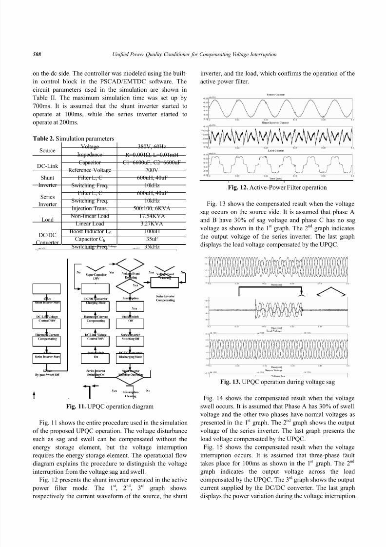
Fig. 11 shows the entire procedure used in the simulationof the proposed UPQC operation. The voltage disturbancesuch as sag and swell can be compensated without theenergy storage element, but the voltage interruptionrequires the energy storage element. The operational flowdiagram explains the procedure to distinguish the voltageinterruption from the voltage sag and swell.
Fig. 12 presents the shunt inverter operated in the active power filter mode. The 1 st, 2nd, 3 rd graph showsrespectively the current waveform of the source, the shunt
inverter, and the load, which confirms the operation of theactive power filter.
Fig. 12. Active-Power Filter operation
Fig. 13 shows the compensated result when the voltagesag occurs on the source side. It is assumed that phase Aand B have 30% of sag voltage and phase C has no sagvoltage as shown in the 1 st graph. The 2 nd graph indicatesthe output voltage of the series inverter. The last graphdisplays the load voltage compensated by the UPQC.
Fig. 13. UPQC operation during voltage sag
Fig. 14 shows the compensated result when the voltageswell occurs. It is assumed that Phase A has 30% of swellvoltage and the other two phases have normal voltages as
presented in the 1 st graph. The 2 nd graph shows the outputvoltage of the series inverter. The last graph presents theload voltage compensated by the UPQC.
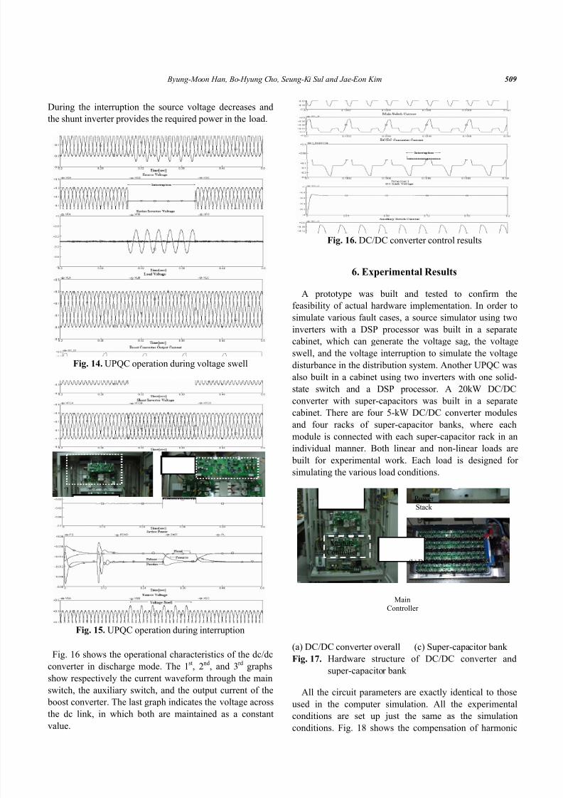
Fig. 15 shows the compensated result when the voltageinterruption occurs. It is assumed that three-phase faulttakes place for 100ms as shown in the 1 st graph. The 2 nd graph indicates the output voltage across the load
compensated by the UPQC. The 3 rd graph shows the outputcurrent supplied by the DC/DC converter. The last graphdisplays the power variation during the voltage interruption.
8/10/2019 Unified Power Quality Conditioner for Compensating Voltage Interruption
510 Unified Power Quality Conditioner for Compensating Voltage Interruption
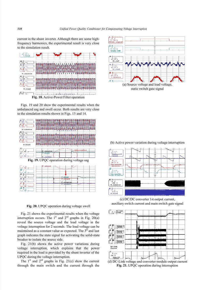
current in the shunt inverter. Although there are some high-frequency harmonics, the experimental result is very closeto the simulation result.
Fig. 18. Active-Power Filter operation
Figs. 19 and 20 show the experimental results when theunbalanced sag and swell occur. Both results are very closeto the simulation results shown in Figs. 13 and 14.
Fig. 19. UPQC operation during voltage sag
Fig. 20. UPQC operation during voltage swell
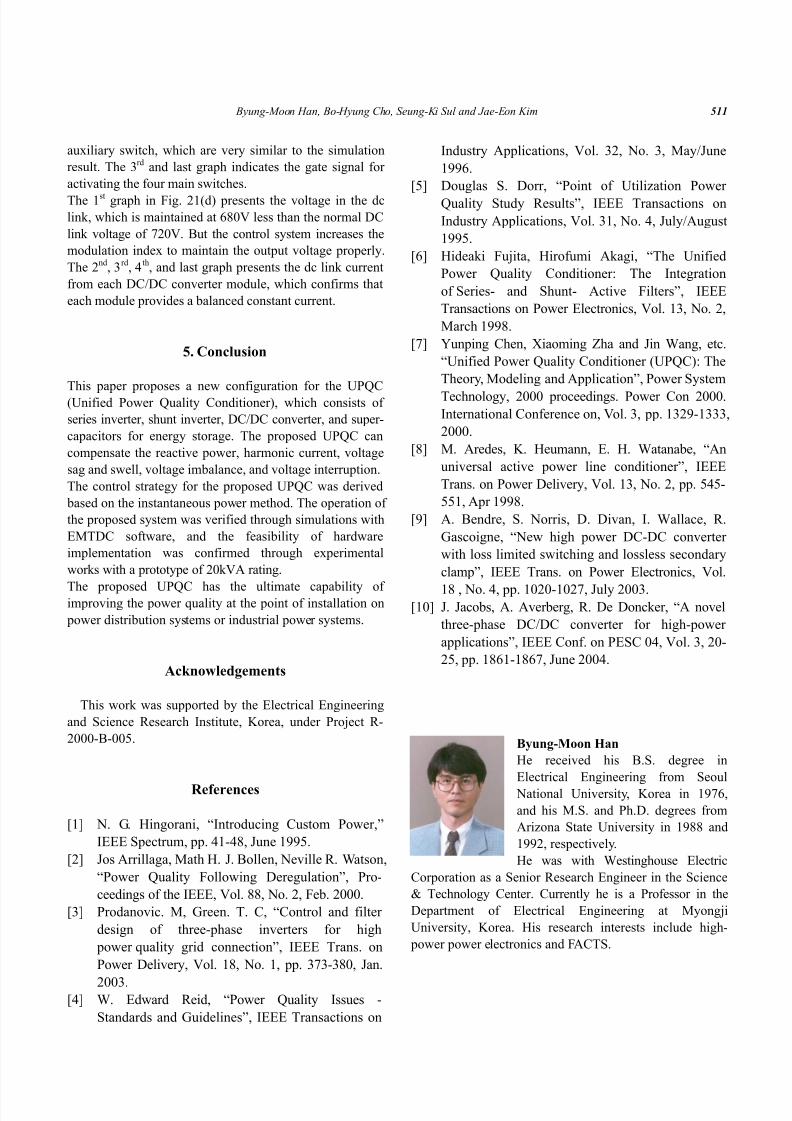
Fig. 21 shows the experimental results when the voltageinterruption occurs. The 1 st and 2 nd graphs in Fig. 20(a)reveal the source voltage and the load voltage in thevoltage interruption for 2 seconds. The load voltage can bemaintained as a constant value as expected. The 3 rd and lastgraph indicates the state signal for activating the solid-state
breaker to isolate the source side.Fig. 21(b) shows the active power variations during
voltage interruption, which explains that the power
required in the load is provided by the shunt inverter of theUPQC during the voltage interruption.The 1 st and 2 nd graphs in Fig. 21(c) show the current
through the main switch and the current through the
(a) Source voltage and load voltage,static switch gate signal
(b) Active power variation during voltage interruption
(c) DC/DC converter 1st output current,
auxiliary switch current and main switch gate signal
(d) DC-Link voltage and converter module output currentFig. 21. UPQC operation during interruption
8/10/2019 Unified Power Quality Conditioner for Compensating Voltage Interruption
Byung-Moon Han, Bo-Hyung Cho, Seung-Ki Sul and Jae-Eon Kim 511
auxiliary switch, which are very similar to the simulationresult. The 3 rd and last graph indicates the gate signal foractivating the four main switches.The 1 st graph in Fig. 21(d) presents the voltage in the dclink, which is maintained at 680V less than the normal DClink voltage of 720V. But the control system increases themodulation index to maintain the output voltage properly.The 2 nd, 3 rd, 4 th, and last graph presents the dc link currentfrom each DC/DC converter module, which confirms thateach module provides a balanced constant current.
5. Conclusion
This paper proposes a new configuration for the UPQC(Unified Power Quality Conditioner), which consists ofseries inverter, shunt inverter, DC/DC converter, and super-capacitors for energy storage. The proposed UPQC cancompensate the reactive power, harmonic current, voltagesag and swell, voltage imbalance, and voltage interruption.The control strategy for the proposed UPQC was derived
based on the instantaneous power method. The operation ofthe proposed system was verified through simulations withEMTDC software, and the feasibility of hardwareimplementation was confirmed through experimentalworks with a prototype of 20kVA rating.
The proposed UPQC has the ultimate capability ofimproving the power quality at the point of installation on
power distribution systems or industrial power systems.
Acknowledgements
This work was supported by the Electrical Engineeringand Science Research Institute, Korea, under Project R-2000-B-005.
References
[1] N. G. Hingorani, “Introducing Custom Power,”IEEE Spectrum, pp. 41-48, June 1995.
[2] Jos Arrillaga, Math H. J. Bollen, Neville R. Watson,“Power Quality Following Deregulation”, Pro-ceedings of the IEEE, Vol. 88, No. 2, Feb. 2000.
[3] Prodanovic. M, Green. T. C, “Control and filterdesign of three-phase inverters for high
power quality grid connection”, IEEE Trans. onPower Delivery, Vol. 18, No. 1, pp. 373-380, Jan.
2003.[4] W. Edward Reid, “Power Quality Issues -
Standards and Guidelines”, IEEE Transactions on
Industry Applications, Vol. 32, No. 3, May/June1996.
[5] Douglas S. Dorr, “Point of Utilization PowerQuality Study Results”, IEEE Transactions onIndustry Applications, Vol. 31, No. 4, July/August1995.
[6] Hideaki Fujita, Hirofumi Akagi, “The UnifiedPower Quality Conditioner: The Integrationof Series- and Shunt- Active Filters”, IEEETransactions on Power Electronics, Vol. 13, No. 2,March 1998.
[7] Yunping Chen, Xiaoming Zha and Jin Wang, etc.“Unified Power Quality Conditioner (UPQC): TheTheory, Modeling and Application”, Power SystemTechnology, 2000 proceedings. Power Con 2000.International Conference on, Vol. 3, pp. 1329-1333,2000.
[8] M. Aredes, K. Heumann, E. H. Watanabe, “Anuniversal active power line conditioner”, IEEETrans. on Power Delivery, Vol. 13, No. 2, pp. 545-551, Apr 1998.
[9] A. Bendre, S. Norris, D. Divan, I. Wallace, R.Gascoigne, “New high power DC-DC converterwith loss limited switching and lossless secondaryclamp”, IEEE Trans. on Power Electronics, Vol.
18 , No. 4, pp. 1020-1027, July 2003.[10] J. Jacobs, A. Averberg, R. De Doncker, “A novel
three-phase DC/DC converter for high-powerapplications”, IEEE Conf. on PESC 04, Vol. 3, 20-25, pp. 1861-1867, June 2004.
Byung-Moon HanHe received his B.S. degree inElectrical Engineering from Seoul
National University, Korea in 1976,and his M.S. and Ph.D. degrees fromArizona State University in 1988 and1992, respectively.He was with Westinghouse Electric
Corporation as a Senior Research Engineer in the Science& Technology Center. Currently he is a Professor in theDepartment of Electrical Engineering at MyongjiUniversity, Korea. His research interests include high-
power power electronics and FACTS.
8/10/2019 Unified Power Quality Conditioner for Compensating Voltage Interruption
512 Unified Power Quality Conditioner for Compensating Voltage Interruption
Bo-Hyung ChoHe received his B.S. and M.E. degreesfrom the California Institute ofTechnology, Pasadena and his Ph.D.degree from the Virginia PolytechnicInstitute and State University (VirginiaTech), Blacksburg, all in Electrical
Engineering.Prior to his research at Virginia Tech, he worked for twoyears as a Member of the Technical Staff in the PowerConversion Electronics Department, TRW Defense andSpace System Group, where he was involved in the designand analysis of spacecraft power processing equipment.From 1982 to 1995, he was a Professor in the Departmentof Electrical Engineering, Virginia Tech. He joined theSchool of Electrical Engineering, Seoul NationalUniversity, Seoul, Korea, in 1995, where he is a Professor.His main research interests include power electronics,modeling, analysis and control of spacecraft power
processing equipment, power systems for space stationsand space platforms, and distributed power systems. Dr.Cho received the 1989 Presidential Young InvestigatorAward from the National Science Foundation. He is amember of Tau Beta Pi.
Seung-Ki Sul
He received his B.S., M.S., and Ph.D.degrees in Electrical Engineering fromSeoul National University, Korea, in1980, 1983 and 1986, respectively. Hewas with the Department of Electricaland Computer Engineering at theUniversity of Wisconsin-Madison as an
Associate Researcher from 1986 to 1988. After that he joined the Gold-Star Industrial Systems Company as aPrincipal Research Engineer from 1988 to 1990. Since1991, he has been on the Faculty of the School ofElectrical Engineering at Seoul National University, and
now serves as an Associate Professor. His current researchinterests are in power electronic control of electricmachines, electric vehicle drives, and power convertercircuits. He was with the Yaskawa Electric Corporation asa R&D Adviser during his sabbatical leave from Aug. 2003to Aug. 2004.
Jae-Eon KimHe received his B.S. and M.S. degreesfrom the University of Hanyang in1982 and 1984, respectively. He waswith KERI as a Researcher from 1984to 1989; a Senior Researcher form1989 to 1996; and a Team Leader of
advanced distribution systems and custom power lab. from1997 to 1998. He received his Ph. D. degree from KyotoUniversity, Japan, in 1996. He has been an AssistantProfessor form 1998 to 2004; and an Associate Professorfrom 2004 until now at the Chungbuk National University.His current interest is the analysis of power quality,operation and design of power distribution systems withdistributed generation, and advanced distribution systems.