2/17/2008 1 1 EC1362 Microprocessor and Microcontroller R.Kumudha EEE Department Rajalakshmi Engineering College MICRO CONTROLLER 8051 IV UNIT 2/17/2008 Contents • Introduction • Block Diagram and Pin Description of the 8051 • Instruction format and addressing modes • Interrupt structure • Timer • I/O ports • Serial communication 2/17/2008 2 www.Vidyarthiplus.com www.Vidyarthiplus.com
Transcript
2/17/2008
1
1
EC1362 Microprocessor and Microcontroller
R.Kumudha
EEE Department
Rajalakshmi Engineering College
MICRO CONTROLLER 8051
IV UNIT
2/17/2008
Contents
• Introduction
• Block Diagram and Pin Description of the 8051
• Instruction format and addressing modes
• Interrupt structure
• Timer
• I/O ports
• Serial communication
2/17/2008 2
www.Vidyarthiplus.com
www.Vidyarthiplus.com
2/17/2008
2
The necessary tools for a
microprocessor/controller
• CPU: Central Processing Unit
• I/O: Input /Output
• Bus: Address bus & Data bus
• Memory: RAM & ROM
• Timer
• Interrupt
• Serial Port
• Parallel Port
2/17/2008 3
CPU
General-
Purpose
Micro-
processor
RAM ROM I/O
PortTimer
Serial
COM
Port
Data Bus
Address Bus
General-Purpose Microprocessor System
Microprocessors:
• CPU for Computers
• No RAM, ROM, I/O on CPU chip itself
• Example覲Intel’s x86, Motorola’s 680x0
Many chips on mother’s board
General-purpose microprocessor
www.Vidyarthiplus.com
www.Vidyarthiplus.com
2/17/2008
3
RAM ROM
I/O
PortTimer
Serial
COM
PortMicrocontroller
CPU
• A smaller computer
• On-chip RAM, ROM, I/O ports...
• Example覲Motorola’s 6811, Intel’s 8051, Zilog’s Z8 and PIC 16X
A single chip
Microcontroller :
Microprocessor
• CPU is stand-alone, RAM,
ROM, I/O, timer are separate
• designer can decide on the
amount of ROM, RAM and
I/O ports.
• expansive
• versatility
• general-purpose
Microcontroller
• CPU, RAM, ROM, I/O and
timer are all on a single chip
• fix amount of on-chip ROM,
RAM, I/O ports
• for applications in which cost,
power and space are critical
• single-purpose
Microprocessor vs. Microcontroller
www.Vidyarthiplus.com
www.Vidyarthiplus.com
2/17/2008
4
• Embedded system means the processor is embedded into that
application.
• An embedded product uses a microprocessor or microcontroller
to do one task only.
• In an embedded system, there is only one application software
that is typically burned into ROM.
• Example覲printer, keyboard, video game player
Embedded System
1. meeting the computing needs of the task efficiently and cost
effectively
• speed, the amount of ROM and RAM, the number of I/O
ports and timers, size, packaging, power consumption
• easy to upgrade
• cost per unit
2. availability of software development tools
• assemblers, debuggers, C compilers, emulator, simulator,
technical support
3. wide availability and reliable sources of the microcontrollers.
Three criteria in Choosing a Microcontroller
www.Vidyarthiplus.com
www.Vidyarthiplus.com
2/17/2008
5
Block Diagram
CPU
On-chip
RAM
On-chip
ROM for
program
code
4 I/O Ports
Timer 0
Serial
PortOSC
Interrupt
Control
External interrupts
Timer 1
Timer/Counter
Bus
Control
TxD RxDP0 P1 P2 P3
Address/Data
Counter
Inputs
Sunday, February 17,
2008
Mahdi Hassanpour
Feature 8051 8052 8031
ROM (program space in bytes) 4K 8K 0K
RAM (bytes) 128 256 128
Timers 2 3 2
I/O pins 32 32 32
Serial port 1 1 1
Interrupt sources 6 8 6
Comparison of the 8051 Family Members
www.Vidyarthiplus.com
www.Vidyarthiplus.com
2/17/2008
6
Pin Description of the 8051Pin Description of the 8051
1
23
45
6
78
91011
1213
1415
161718
1920
40
3938
3736
35
3433
323130
2928
2726
252423
2221
P1.0P1.1P1.2
P1.3P1.4
P1.5
P1.6P1.7
RST(RXD)P3.0(TXD)P3.1
(T0)P3.4(T1)P3.5
XTAL2
XTAL1GND
(INT0)P3.2
(INT1)P3.3
(RD)P3.7(WR)P3.6
VccP0.0(AD0)P0.1(AD1)
P0.2(AD2)P0.3(AD3)
P0.4(AD4)
P0.5(AD5)P0.6(AD6)
P0.7(AD7)
EA/VPPALE/PROG
PSENP2.7(A15)
P2.6(A14)P2.5(A13)P2.4(A12)
P2.3(A11)
P2.2(A10)P2.1(A9)P2.0(A8)
8051
(8031)
www.Vidyarthiplus.com
www.Vidyarthiplus.com
2/17/2008
7
Pins of 8051襦襦襦襦1/4襤襤襤襤
• Vcc襦pin 40襤覲– Vcc provides supply voltage to the chip.
– The voltage source is +5V.
• GND襦pin 20襤覲ground
• XTAL1 and XTAL2襦pins 19,18襤
Figure (a). XTAL Connection to 8051Figure (a). XTAL Connection to 8051
C2
30pF
C1
30pF
XTAL2
XTAL1
GND
� Using a quartz crystal oscillator
� We can observe the frequency on the XTAL2 pin.
www.Vidyarthiplus.com
www.Vidyarthiplus.com
2/17/2008
8
Example :
Find the machine cycle for
(a) XTAL = 11.0592 MHz
(b) XTAL = 16 MHz.
Solution:
(a) 11.0592 MHz / 12 = 921.6 kHz;
machine cycle = 1 / 921.6 kHz = 1.085 µs
(b) 16 MHz / 12 = 1.333 MHz;
machine cycle = 1 / 1.333 MHz = 0.75 µs
Pins of 8051襦襦襦襦2/4襤襤襤襤
• RST襦pin 9襤覲reset
– It is an input pin and is active high襦normally low襤.
• The high pulse must be high at least 2 machine cycles.
– It is a power-on reset.
• Upon applying a high pulse to RST, the
microcontroller will reset and all values in registers
will be lost.
• Reset values of some 8051 registers �
www.Vidyarthiplus.com
www.Vidyarthiplus.com
2/17/2008
9
Figure (b). Power-On RESET Circuit
30 pF
30 pF
8.2 K
10 uF
+
Vcc
11.0592 MHz
EA/VPP
X1
X2
RST
31
19
18
9
Pins of 8051襦襦襦襦3/4襤襤襤襤
• /EA襦pin 31襤覲external access
– There is no on-chip ROM in 8031 and 8032 .
– The /EA pin is connected to GND to indicate the code
is stored externally.
– /PSEN 襠 ALE are used for external ROM.
– For 8051, /EA pin is connected to Vcc.
– “/” means active low.
• /PSEN襦pin 29襤覲program store enable
– This is an output pin and is connected to the OE pin of
the ROM.
www.Vidyarthiplus.com
www.Vidyarthiplus.com
2/17/2008
10
Pins of 8051襦襦襦襦4/4襤襤襤襤
• ALE襦pin 30襤覲address latch enable
– It is an output pin and is active high.
– 8051 port 0 provides both address and data.
– The ALE pin is used for de-multiplexing the address and data by connecting to the G pin of the 74LS373 latch.
• I/O port pins
– The four ports P0, P1, P2, and P3.
– Each port uses 8 pins.
– All I/O pins are bi-directional..
Pins of I/O Port
• The 8051 has four I/O ports
– Port 0 襦pins 32-39襤覲P0襦P0.0譌P0.7襤– Port 1襦pins 1-8襤 覲P1襦P1.0譌P1.7襤– Port 2襦pins 21-28襤覲P2襦P2.0譌P2.7襤– Port 3襦pins 10-17襤覲P3襦P3.0譌P3.7襤– Each port has 8 pins.
• Named P0.X 襦X=0,1,...,7襤, P1.X, P2.X, P3.X
• Ex覲P0.0 is the bit 0襦LSB襤of P0
• Ex覲P0.7 is the bit 7襦MSB襤of P0
• These 8 bits form a byte.
• Each port can be used as input or output (bi-direction).
www.Vidyarthiplus.com
www.Vidyarthiplus.com
2/17/2008
11
Hardware Structure of I/O Pin
• Each pin of I/O ports
– Internal CPU bus覲communicate with CPU
– A D latch store the value of this pin
• D latch is controlled by “Write to latch”
– Write to latch覿1覲write data into the D latch
– 2 Tri-state buffer覲�
• TB1: controlled by “Read pin”
– Read pin覿1覲really read the data present at the pin
• TB2: controlled by “Read latch”
– Read latch覿1覲read value from internal latch
– A transistor M1 gate
• Gate=0: open
• Gate=1: close
D Latch:
www.Vidyarthiplus.com
www.Vidyarthiplus.com
2/17/2008
12
A Pin of Port 1
8051 IC
D Q
Clk Q
Vcc
Load(L1)
Read latch
Read pin
Write to latch
Internal CPU
bus
M1
P1.X
pinP1.X
TB1
TB2
P0.x
Writing “1” to Output Pin P1.X
D Q
Clk Q
Vcc
Load(L1)
Read latch
Read pin
Write to latch
Internal CPU
bus
M1
P1.X
pinP1.X
8051 IC
2. output pin is
Vcc1. write a 1 to the pin
1
0 output 1
TB1
TB2
www.Vidyarthiplus.com
www.Vidyarthiplus.com
2/17/2008
13
Writing “0” to Output Pin P1.X
D Q
Clk Q
Vcc
Load(L1)
Read latch
Read pin
Write to latch
Internal CPU
bus
M1
P1.X
pinP1.X
8051 IC
2. output pin is
ground1. write a 0 to the pin
0
1 output 0
TB1
TB2
Reading “High” at Input Pin
D Q
Clk Q
Vcc
Load(L1)
Read latch
Read pin
Write to latch
Internal CPU bus
M1
P1.X pin
P1.X
8051 IC
2. MOV A,P1
external pin=High1. write a 1 to the pin MOV
P1,#0FFH
1
0
3. Read pin=1 Read latch=0
Write to latch=1
1
TB1
TB2
www.Vidyarthiplus.com
www.Vidyarthiplus.com
2/17/2008
14
Reading “Low” at Input Pin
D Q
Clk Q
Vcc
Load(L1)
Read latch
Read pin
Write to latch
Internal CPU bus
M1
P1.X pin
P1.X
8051 IC
2. MOV A,P1
external pin=Low1. write a 1 to the pin
MOV P1,#0FFH
1
0
3. Read pin=1 Read latch=0
Write to latch=1
0
TB1
TB2
Other Pins
• P1, P2, and P3 have internal pull-up resisters.
– P1, P2, and P3 are not open drain.
• P0 has no internal pull-up resistors and does not connects to Vcc inside the 8051.
– P0 is open drain.
– Compare the figures of P1.X and P0.X. �
• However, for a programmer, it is the same to program P0, P1, P2 and P3.
• All the ports upon RESET are configured as output.
www.Vidyarthiplus.com
www.Vidyarthiplus.com
2/17/2008
15
A Pin of Port 0
8051 IC
D Q
Clk Q
Read latch
Read pin
Write to latch
Internal CPU
bus
M1
P0.X
pinP1.X
TB1
TB2
P1.x
Port 0 with Pull-Up Resistors
P0.0P0.1P0.2P0.3P0.4P0.5P0.6P0.7
DS5000
8751
8951
Vcc10 K
Port
0
www.Vidyarthiplus.com
www.Vidyarthiplus.com
2/17/2008
16
Port 3 Alternate Functions
1717RDRDP3.7P3.7
1616WRWRP3.6P3.6
1515T1T1PP33..55
1414T0T0P3.4P3.4
1313INTINT11P3.3P3.3
1212INT0INT0P3.2P3.2
1111TxDTxDP3.1P3.1
1010RxDRxDP3.0P3.0
PinPinFunctionFunctionPP3 3 BitBit
RESET Value of Some 8051 Registers:
0000DPTR
0007SP
0000PSW
0000B
0000ACC
0000PC
Reset ValueRegister
RAM are all zero..
www.Vidyarthiplus.com
www.Vidyarthiplus.com
2/17/2008
17
Registers
A
B
R0
R1
R3
R4
R2
R5
R7
R6
DPH DPL
PC
DPTR
PC
Some 8051 16-bit Register
Some 8-bitt Registers of
the 8051
Addressing Modes
There are eight addressing modes available in the 8051:
• Register
• Direct
• Indirect
• Immediate
• Relative
• Absolute
• Long
• Indexed
www.Vidyarthiplus.com
www.Vidyarthiplus.com
2/17/2008
18
Immediate Addressing
• With one exception, all instructions using
immediate addressing use 8-bit data
• Exception: when initializing the data pointer, a 16-
bit constant is required
• Example: MOV DPTR, #8000H
2/17/2008 35
Immediate Addressing Mode
MOV A,#65H
MOV A,#’A’
MOV R6,#65H
MOV DPTR,#2343H
MOV P1,#65H
Example :
Num EQU 30
…
MOV R0,Num
MOV DPTR,#data1
…
ORG 100H
data1: db “IRAN”
www.Vidyarthiplus.com
www.Vidyarthiplus.com
2/17/2008
19
Register Addressing• 8051 has access to eight working registers (R0 to R7)
• Instructions using register addressing are encoded using the
three least significant bits of the instruction opcode to specify a
register
• Example: ADD A,R7
• The opcode is 00101111. 00101 indicates the instruction and the
three lower bits, 111, specify the register
• Some instructions are specific to a certain register, such as the
accumulator, data pointer etc.
• • Example: INC DPTR
• – A 1-byte instruction adding 1 to the data pointer
• • Example: MUL AB
• – A 1-byte instruction multiplying unsigned values in
accumulator and register B2/17/2008 37
Register Addressing Mode
MOV Rn, A ;n=0,..,7
ADD A, Rn
MOV DPL, R6
MOV DPTR, A
MOV Rm, Rn
www.Vidyarthiplus.com
www.Vidyarthiplus.com
2/17/2008
20
Direct Addressing
• Direct addressing can access any on-chip memory location
• Example: ADD A,55H
• Example: MOV P1, A
– Transfers the content of accumulator to Port 1 (address
90H)
2/17/2008 39
Sunday, February 17,
2008
Mahdi Hassanpour
Direct Addressing Mode
Although the entire of 128 bytes of RAM can be accessed using direct addressing mode, it is most often used to access RAM loc. 30 – 7FH.
MOV R0, 40H
MOV 56H, A
MOV A, 4 ; ≡ MOV A, R4
MOV 6, 2 ; copy R2 to R6
; MOV R6,R2 is invalid !
SFR register and their address
MOV 0E0H, #66H ; ≡ MOV A,#66H
MOV 0F0H, R2 ; ≡ MOV B, R2
MOV 80H,A ; ≡ MOV P1,A
Bit Addressable
Page 359,360
www.Vidyarthiplus.com
www.Vidyarthiplus.com
2/17/2008
21
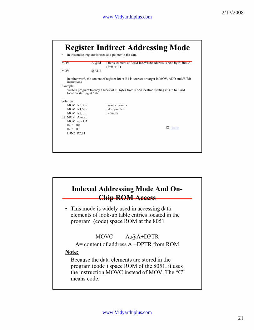
Register Indirect Addressing Mode• In this mode, register is used as a pointer to the data.
MOV A,@Ri ; move content of RAM loc.Where address is held by Ri into A
( i=0 or 1 )
MOV @R1,B
In other word, the content of register R0 or R1 is sources or target in MOV, ADD and SUBB insructions.
Example:
Write a program to copy a block of 10 bytes from RAM location sterting at 37h to RAM location starting at 59h.
Solution:
MOV R0,37h ; source pointer
MOV R1,59h ; dest pointer
MOV R2,10 ; counter
L1: MOV A,@R0
MOV @R1,A
INC R0
INC R1
DJNZ R2,L1
jump
Indexed Addressing Mode And On-
Chip ROM Access
• This mode is widely used in accessing data elements of look-up table entries located in the program (code) space ROM at the 8051
MOVC A,@A+DPTR
A= content of address A +DPTR from ROM
Note:
Because the data elements are stored in the program (code ) space ROM of the 8051, it uses the instruction MOVC instead of MOV. The “C” means code.
www.Vidyarthiplus.com
www.Vidyarthiplus.com
2/17/2008
22
Relative Addressing• Relative addressing is used with certain jump instructions
• Relative address (offset) is an 8-bit signed value (-128 to 127)
• which is added to the program counter to form the address of
• next instruction
• Prior to addition, the program counter is incremented to the
• address following the jump (the new address is relative to the
• next instruction, not the address of the jump instruction)
• This detail is of no concern to the user since the jump
• destinations are usually specified as labels and the assembler
• determines the relative offset
• Advantage of relative addressing: position independent codes
2/17/2008 43
Absolute Addressing
• Absolute addressing is only used with ACALL
and AJMP
• • The 11 least significant bits of the destination
address comes from the opcode and the upper five
bits are the current upper five bits in the program
counter (PC).
• • The destination is in the same 2K (211) of the
source
2/17/2008 44
www.Vidyarthiplus.com
www.Vidyarthiplus.com
2/17/2008
23
Long Addressing
• Long addressing is used only with the LCALL and
LJMP instructions
• These 3-bytes instructions include a full 16-bit
destination address as bytes 2 and 3
• The full 64K code space is available
• The instruction is long and position dependent
• Example: LJMP, 8AF2H
• Jumps to memory location 8AF2H
2/17/2008 45
Indexed Addressing
• Indexed addressing uses a base register (either the
program counter or data pointer) and an offset (the
accumulator) in forming the effective address for a
JMP or MOVC instruction
• Example: MOVC A, @A+DPTR
– This instruction moves a byte of data from code
memory
to the accumulator. The address in code memory is
found by adding the accumulator to the data pointer
2/17/2008 46
www.Vidyarthiplus.com
www.Vidyarthiplus.com
2/17/2008
24
Sunday, February 17,
2008
Mahdi Hassanpour
• Example:
Assuming that ROM space starting at 250h contains “Hello.”, write a program to transfer the bytes into RAM locations starting at 40h.
Solution:
ORG 0
MOV DPTR,#MYDATA
MOV R0,#40H
L1: CLR A
MOVC A,@A+DPTR
JZ L2
MOV @R0,A
INC DPTR
INC R0
SJMP L1
L2: SJMP L2
;-------------------------------------
ORG 250H
MYDATA: DB “Hello”,0
END
Notice the NULL character ,0, as end of string and how we use the JZ instruction to detect that.
Sunday, February 17,
2008
Mahdi Hassanpour
• Example:
Write a program to get the x value from P1 and send x2 to P2, continuously .
• Gate : When set, timer only runs while INT(0,1) is high.
• C/T : Counter/Timer select bit.
• M1 : Mode bit 1.
• M0 : Mode bit 0.
TCON Register:
• TF1: Timer 1 overflow flag.
• TR1: Timer 1 run control bit.
• TF0: Timer 0 overflag.
• TR0: Timer 0 run control bit.
• IE1: External interrupt 1 edge flag.
• IT1: External interrupt 1 type flag.
• IE0: External interrupt 0 edge flag.
• IT0: External interrupt 0 type flag.
www.Vidyarthiplus.com
www.Vidyarthiplus.com
2/17/2008
26
Interrupt :
Interrupt Enable Register :
• EA : Global enable/disable.• --- : Undefined.
• ET2 :Enable Timer 2 interrupt.
• ES :Enable Serial port interrupt.
• ET1 :Enable Timer 1 interrupt.
• EX1 :Enable External 1 interrupt.
• ET0 : Enable Timer 0 interrupt.
• EX0 : Enable External 0 interrupt.
www.Vidyarthiplus.com
www.Vidyarthiplus.com
2/17/2008
1
1
EC1362 Microprocessor and Microcontroller
R.Kumudha
EEE Department
Rajalakshmi Engineering College
MICRO CONTROLLER 8051
IV UNIT
2/17/2008
Contents
• Introduction
• Block Diagram and Pin Description of the 8051
• Instruction format and addressing modes
• Interrupt structure
• Timer
• I/O ports
• Serial communication
2/17/2008 2
www.Vidyarthiplus.com
www.Vidyarthiplus.com
2/17/2008
2
The necessary tools for a
microprocessor/controller
• CPU: Central Processing Unit
• I/O: Input /Output
• Bus: Address bus & Data bus
• Memory: RAM & ROM
• Timer
• Interrupt
• Serial Port
• Parallel Port
2/17/2008 3
CPU
General-
Purpose
Micro-
processor
RAM ROM I/O
PortTimer
Serial
COM
Port
Data Bus
Address Bus
General-Purpose Microprocessor System
Microprocessors:
• CPU for Computers
• No RAM, ROM, I/O on CPU chip itself
• Example:Intel’s x86, Motorola’s 680x0
Many chips on mother’s board
General-purpose microprocessor
www.Vidyarthiplus.com
www.Vidyarthiplus.com
2/17/2008
3
RAM ROM
I/O
PortTimer
Serial
COM
PortMicrocontroller
CPU
• A smaller computer
• On-chip RAM, ROM, I/O ports...
• Example:Motorola’s 6811, Intel’s 8051, Zilog’s Z8 and PIC 16X
A single chip
Microcontroller :
Microprocessor
• CPU is stand-alone, RAM,
ROM, I/O, timer are separate
• designer can decide on the
amount of ROM, RAM and
I/O ports.
• expansive
• versatility
• general-purpose
Microcontroller
• CPU, RAM, ROM, I/O and
timer are all on a single chip
• fix amount of on-chip ROM,
RAM, I/O ports
• for applications in which cost,
power and space are critical
• single-purpose
Microprocessor vs. Microcontroller
www.Vidyarthiplus.com
www.Vidyarthiplus.com
2/17/2008
4
• Embedded system means the processor is embedded into that
application.
• An embedded product uses a microprocessor or microcontroller
to do one task only.
• In an embedded system, there is only one application software
that is typically burned into ROM.
• Example:printer, keyboard, video game player
Embedded System
1. meeting the computing needs of the task efficiently and cost
effectively
• speed, the amount of ROM and RAM, the number of I/O
ports and timers, size, packaging, power consumption
• easy to upgrade
• cost per unit
2. availability of software development tools
• assemblers, debuggers, C compilers, emulator, simulator,
technical support
3. wide availability and reliable sources of the microcontrollers.
Three criteria in Choosing a Microcontroller
www.Vidyarthiplus.com
www.Vidyarthiplus.com
2/17/2008
5
Block Diagram
CPU
On-chip
RAM
On-chip
ROM for
program
code
4 I/O Ports
Timer 0
Serial
PortOSC
Interrupt
Control
External interrupts
Timer 1
Timer/Counter
Bus
Control
TxD RxDP0 P1 P2 P3
Address/Data
Counter
Inputs
Sunday, February 17,
2008
Mahdi Hassanpour
Feature 8051 8052 8031
ROM (program space in bytes) 4K 8K 0K
RAM (bytes) 128 256 128
Timers 2 3 2
I/O pins 32 32 32
Serial port 1 1 1
Interrupt sources 6 8 6
Comparison of the 8051 Family Members
www.Vidyarthiplus.com
www.Vidyarthiplus.com
2/17/2008
6
Pin Description of the 8051Pin Description of the 8051
1
23
45
6
78
91011
1213
1415
161718
1920
40
3938
3736
35
3433
323130
2928
2726
252423
2221
P1.0P1.1P1.2
P1.3P1.4
P1.5
P1.6P1.7
RST(RXD)P3.0(TXD)P3.1
(T0)P3.4(T1)P3.5
XTAL2
XTAL1GND
(INT0)P3.2
(INT1)P3.3
(RD)P3.7(WR)P3.6
VccP0.0(AD0)P0.1(AD1)
P0.2(AD2)P0.3(AD3)
P0.4(AD4)
P0.5(AD5)P0.6(AD6)
P0.7(AD7)
EA/VPPALE/PROG
PSENP2.7(A15)
P2.6(A14)P2.5(A13)P2.4(A12)
P2.3(A11)
P2.2(A10)P2.1(A9)P2.0(A8)
8051
(8031)
www.Vidyarthiplus.com
www.Vidyarthiplus.com
2/17/2008
7
Pins of 8051((((1/4))))
• Vcc(pin 40):– Vcc provides supply voltage to the chip.
– The voltage source is +5V.
• GND(pin 20):ground
• XTAL1 and XTAL2(pins 19,18)
Figure (a). XTAL Connection to 8051Figure (a). XTAL Connection to 8051
C2
30pF
C1
30pF
XTAL2
XTAL1
GND
� Using a quartz crystal oscillator
� We can observe the frequency on the XTAL2 pin.
www.Vidyarthiplus.com
www.Vidyarthiplus.com
2/17/2008
8
Example :
Find the machine cycle for
(a) XTAL = 11.0592 MHz
(b) XTAL = 16 MHz.
Solution:
(a) 11.0592 MHz / 12 = 921.6 kHz;
machine cycle = 1 / 921.6 kHz = 1.085 µs
(b) 16 MHz / 12 = 1.333 MHz;
machine cycle = 1 / 1.333 MHz = 0.75 µs
Pins of 8051((((2/4))))
• RST(pin 9):reset
– It is an input pin and is active high(normally low).
• The high pulse must be high at least 2 machine cycles.
– It is a power-on reset.
• Upon applying a high pulse to RST, the
microcontroller will reset and all values in registers
will be lost.
• Reset values of some 8051 registers �
www.Vidyarthiplus.com
www.Vidyarthiplus.com
2/17/2008
9
Figure (b). Power-On RESET Circuit
30 pF
30 pF
8.2 K
10 uF
+
Vcc
11.0592 MHz
EA/VPP
X1
X2
RST
31
19
18
9
Pins of 8051((((3/4))))
• /EA(pin 31):external access
– There is no on-chip ROM in 8031 and 8032 .
– The /EA pin is connected to GND to indicate the code
is stored externally.
– /PSEN & ALE are used for external ROM.
– For 8051, /EA pin is connected to Vcc.
– “/” means active low.
• /PSEN(pin 29):program store enable
– This is an output pin and is connected to the OE pin of
the ROM.
www.Vidyarthiplus.com
www.Vidyarthiplus.com
2/17/2008
10
Pins of 8051((((4/4))))
• ALE(pin 30):address latch enable
– It is an output pin and is active high.
– 8051 port 0 provides both address and data.
– The ALE pin is used for de-multiplexing the address and data by connecting to the G pin of the 74LS373 latch.
• I/O port pins
– The four ports P0, P1, P2, and P3.
– Each port uses 8 pins.
– All I/O pins are bi-directional..
Pins of I/O Port
• The 8051 has four I/O ports
– Port 0 (pins 32-39):P0(P0.0~P0.7)– Port 1(pins 1-8) :P1(P1.0~P1.7)– Port 2(pins 21-28):P2(P2.0~P2.7)– Port 3(pins 10-17):P3(P3.0~P3.7)– Each port has 8 pins.
• Named P0.X (X=0,1,...,7), P1.X, P2.X, P3.X
• Ex:P0.0 is the bit 0(LSB)of P0
• Ex:P0.7 is the bit 7(MSB)of P0
• These 8 bits form a byte.
• Each port can be used as input or output (bi-direction).
www.Vidyarthiplus.com
www.Vidyarthiplus.com
2/17/2008
11
Hardware Structure of I/O Pin
• Each pin of I/O ports
– Internal CPU bus:communicate with CPU
– A D latch store the value of this pin
• D latch is controlled by “Write to latch”
– Write to latch=1:write data into the D latch
– 2 Tri-state buffer:�
• TB1: controlled by “Read pin”
– Read pin=1:really read the data present at the pin
• TB2: controlled by “Read latch”
– Read latch=1:read value from internal latch
– A transistor M1 gate
• Gate=0: open
• Gate=1: close
D Latch:
www.Vidyarthiplus.com
www.Vidyarthiplus.com
2/17/2008
12
A Pin of Port 1
8051 IC
D Q
Clk Q
Vcc
Load(L1)
Read latch
Read pin
Write to latch
Internal CPU
bus
M1
P1.X
pinP1.X
TB1
TB2
P0.x
Writing “1” to Output Pin P1.X
D Q
Clk Q
Vcc
Load(L1)
Read latch
Read pin
Write to latch
Internal CPU
bus
M1
P1.X
pinP1.X
8051 IC
2. output pin is
Vcc1. write a 1 to the pin
1
0 output 1
TB1
TB2
www.Vidyarthiplus.com
www.Vidyarthiplus.com
2/17/2008
13
Writing “0” to Output Pin P1.X
D Q
Clk Q
Vcc
Load(L1)
Read latch
Read pin
Write to latch
Internal CPU
bus
M1
P1.X
pinP1.X
8051 IC
2. output pin is
ground1. write a 0 to the pin
0
1 output 0
TB1
TB2
Reading “High” at Input Pin
D Q
Clk Q
Vcc
Load(L1)
Read latch
Read pin
Write to latch
Internal CPU bus
M1
P1.X pin
P1.X
8051 IC
2. MOV A,P1
external pin=High1. write a 1 to the pin MOV
P1,#0FFH
1
0
3. Read pin=1 Read latch=0
Write to latch=1
1
TB1
TB2
www.Vidyarthiplus.com
www.Vidyarthiplus.com
2/17/2008
14
Reading “Low” at Input Pin
D Q
Clk Q
Vcc
Load(L1)
Read latch
Read pin
Write to latch
Internal CPU bus
M1
P1.X pin
P1.X
8051 IC
2. MOV A,P1
external pin=Low1. write a 1 to the pin
MOV P1,#0FFH
1
0
3. Read pin=1 Read latch=0
Write to latch=1
0
TB1
TB2
Other Pins
• P1, P2, and P3 have internal pull-up resisters.
– P1, P2, and P3 are not open drain.
• P0 has no internal pull-up resistors and does not connects to Vcc inside the 8051.
– P0 is open drain.
– Compare the figures of P1.X and P0.X. �
• However, for a programmer, it is the same to program P0, P1, P2 and P3.
• All the ports upon RESET are configured as output.
www.Vidyarthiplus.com
www.Vidyarthiplus.com
2/17/2008
15
A Pin of Port 0
8051 IC
D Q
Clk Q
Read latch
Read pin
Write to latch
Internal CPU
bus
M1
P0.X
pinP1.X
TB1
TB2
P1.x
Port 0 with Pull-Up Resistors
P0.0P0.1P0.2P0.3P0.4P0.5P0.6P0.7
DS5000
8751
8951
Vcc10 K
Port
0
www.Vidyarthiplus.com
www.Vidyarthiplus.com
2/17/2008
16
Port 3 Alternate Functions
1717RDRDP3.7P3.7
1616WRWRP3.6P3.6
1515T1T1P3.5P3.5
1414T0T0P3.4P3.4
1313INTINT11P3.3P3.3
1212INT0INT0P3.2P3.2
1111TxDTxDP3.1P3.1
1010RxDRxDP3.0P3.0
PinPinFunctionFunctionPP3 3 BitBit
RESET Value of Some 8051 Registers:
0000DPTR
0007SP
0000PSW
0000B
0000ACC
0000PC
Reset ValueRegister
RAM are all zero..
www.Vidyarthiplus.com
www.Vidyarthiplus.com
2/17/2008
17
Registers
A
B
R0
R1
R3
R4
R2
R5
R7
R6
DPH DPL
PC
DPTR
PC
Some 8051 16-bit Register
Some 8-bitt Registers of
the 8051
Addressing Modes
There are eight addressing modes available in the 8051:
• Register
• Direct
• Indirect
• Immediate
• Relative
• Absolute
• Long
• Indexed
www.Vidyarthiplus.com
www.Vidyarthiplus.com
2/17/2008
18
Immediate Addressing
• With one exception, all instructions using
immediate addressing use 8-bit data
• Exception: when initializing the data pointer, a 16-
bit constant is required
• Example: MOV DPTR, #8000H
2/17/2008 35
Immediate Addressing Mode
MOV A,#65H
MOV A,#’A’
MOV R6,#65H
MOV DPTR,#2343H
MOV P1,#65H
Example :
Num EQU 30
…
MOV R0,Num
MOV DPTR,#data1
…
ORG 100H
data1: db “IRAN”
www.Vidyarthiplus.com
www.Vidyarthiplus.com
2/17/2008
19
Register Addressing• 8051 has access to eight working registers (R0 to R7)
• Instructions using register addressing are encoded using the
three least significant bits of the instruction opcode to specify a
register
• Example: ADD A,R7
• The opcode is 00101111. 00101 indicates the instruction and the
three lower bits, 111, specify the register
• Some instructions are specific to a certain register, such as the
accumulator, data pointer etc.
• • Example: INC DPTR
• – A 1-byte instruction adding 1 to the data pointer
• • Example: MUL AB
• – A 1-byte instruction multiplying unsigned values in
accumulator and register B2/17/2008 37
Register Addressing Mode
MOV Rn, A ;n=0,..,7
ADD A, Rn
MOV DPL, R6
MOV DPTR, A
MOV Rm, Rn
www.Vidyarthiplus.com
www.Vidyarthiplus.com
2/17/2008
20
Direct Addressing
• Direct addressing can access any on-chip memory location
• Example: ADD A,55H
• Example: MOV P1, A
– Transfers the content of accumulator to Port 1 (address
90H)
2/17/2008 39
Sunday, February 17,
2008
Mahdi Hassanpour
Direct Addressing Mode
Although the entire of 128 bytes of RAM can be accessed using direct addressing mode, it is most often used to access RAM loc. 30 – 7FH.
MOV R0, 40H
MOV 56H, A
MOV A, 4 ; ≡ MOV A, R4
MOV 6, 2 ; copy R2 to R6
; MOV R6,R2 is invalid !
SFR register and their address
MOV 0E0H, #66H ; ≡ MOV A,#66H
MOV 0F0H, R2 ; ≡ MOV B, R2
MOV 80H,A ; ≡ MOV P1,A
Bit Addressable
Page 359,360
www.Vidyarthiplus.com
www.Vidyarthiplus.com
2/17/2008
21
Register Indirect Addressing Mode• In this mode, register is used as a pointer to the data.
MOV A,@Ri ; move content of RAM loc.Where address is held by Ri into A
( i=0 or 1 )
MOV @R1,B
In other word, the content of register R0 or R1 is sources or target in MOV, ADD and SUBB insructions.
Example:
Write a program to copy a block of 10 bytes from RAM location sterting at 37h to RAM location starting at 59h.
Solution:
MOV R0,37h ; source pointer
MOV R1,59h ; dest pointer
MOV R2,10 ; counter
L1: MOV A,@R0
MOV @R1,A
INC R0
INC R1
DJNZ R2,L1
jump
Indexed Addressing Mode And On-
Chip ROM Access
• This mode is widely used in accessing data elements of look-up table entries located in the program (code) space ROM at the 8051
MOVC A,@A+DPTR
A= content of address A +DPTR from ROM
Note:
Because the data elements are stored in the program (code ) space ROM of the 8051, it uses the instruction MOVC instead of MOV. The “C” means code.
www.Vidyarthiplus.com
www.Vidyarthiplus.com
2/17/2008
22
Relative Addressing• Relative addressing is used with certain jump instructions
• Relative address (offset) is an 8-bit signed value (-128 to 127)
• which is added to the program counter to form the address of
• next instruction
• Prior to addition, the program counter is incremented to the
• address following the jump (the new address is relative to the
• next instruction, not the address of the jump instruction)
• This detail is of no concern to the user since the jump
• destinations are usually specified as labels and the assembler
• determines the relative offset
• Advantage of relative addressing: position independent codes
2/17/2008 43
Absolute Addressing
• Absolute addressing is only used with ACALL
and AJMP
• • The 11 least significant bits of the destination
address comes from the opcode and the upper five
bits are the current upper five bits in the program
counter (PC).
• • The destination is in the same 2K (211) of the
source
2/17/2008 44
www.Vidyarthiplus.com
www.Vidyarthiplus.com
2/17/2008
23
Long Addressing
• Long addressing is used only with the LCALL and
LJMP instructions
• These 3-bytes instructions include a full 16-bit
destination address as bytes 2 and 3
• The full 64K code space is available
• The instruction is long and position dependent
• Example: LJMP, 8AF2H
• Jumps to memory location 8AF2H
2/17/2008 45
Indexed Addressing
• Indexed addressing uses a base register (either the
program counter or data pointer) and an offset (the
accumulator) in forming the effective address for a
JMP or MOVC instruction
• Example: MOVC A, @A+DPTR
– This instruction moves a byte of data from code
memory
to the accumulator. The address in code memory is
found by adding the accumulator to the data pointer
2/17/2008 46
www.Vidyarthiplus.com
www.Vidyarthiplus.com
2/17/2008
24
Sunday, February 17,
2008
Mahdi Hassanpour
• Example:
Assuming that ROM space starting at 250h contains “Hello.”, write a program to transfer the bytes into RAM locations starting at 40h.
Solution:
ORG 0
MOV DPTR,#MYDATA
MOV R0,#40H
L1: CLR A
MOVC A,@A+DPTR
JZ L2
MOV @R0,A
INC DPTR
INC R0
SJMP L1
L2: SJMP L2
;-------------------------------------
ORG 250H
MYDATA: DB “Hello”,0
END
Notice the NULL character ,0, as end of string and how we use the JZ instruction to detect that.
Sunday, February 17,
2008
Mahdi Hassanpour
• Example:
Write a program to get the x value from P1 and send x2 to P2, continuously .