Electronic Circuits 10CS32 Unit – 1: Transistor, UJT’ s, and Thyristors In the Diode tutorials we saw that simple diodes are made up from two pieces of semiconductor material, either silicon or germanium to form a simple PN-junction and we also learnt about their properties and characteristics. If we now join together two individual signal diodes back-to-back, this will give us two PN-junctions connected together in series that share a common P or N terminal. The fusion of these two diodes produces a three layer, two junctions, and three terminal devices forming the basis of a Bipolar Junction Transistor, or BJT for short. 1.1 Operating Point Operating Regions The pink shaded area at the bottom of the curves represents the "Cut-off" region while the blue area to the left represents the "Saturation" region of the transistor. Both these transistor regions are defined as: 1. Cut-off Region Here the operating conditions of the transistor are zero input base current (I B ), zero output collector current (I C ) and maximum collector voltage (V CE ) which results in a large depletion layer and no current flowing through the device. Therefore the transistor is switched "Fully- OFF". Page 3 Gechstudentszone.wordpress.com SUMLATA K
Transcript
Electronic Circuits 10CS32
Unit – 1: Transistor, UJT’s, and Thyristors
In the Diode tutorials we saw that simple diodes are made up from two pieces of
semiconductor material, either silicon or germanium to form a simple PN-junction and we
also learnt about their properties and characteristics. If we now join together two individual signal diodes back-to-back, this will give us two PN-junctions connected together in series
that share a common P or N terminal. The fusion of these two diodes produces a three layer, two junctions, and three terminal devices forming the basis of a Bipolar Junction
Transistor, or BJT for short.
1.1 Operating Point
Operating Regions
The pink shaded area at the bottom of the curves represents the "Cut-off" region while the
blue area to the left represents the "Saturation" region of the transistor. Both these transistor
regions are defined as:
1. Cut-off Region
Here the operating conditions of the transistor are zero input base current (IB), zero output
collector current (IC) and maximum collector voltage (VCE) which results in a large depletion
layer and no current flowing through the device. Therefore the transistor is switched "Fully-
OFF".
Page 3
Gechs
tude
ntsz
one.
wordp
ress
.com
SUMLATA K
Electronic Circuits 10CS32
Cut-off Characteristics
The input and Base are grounded (0v) Base-Emitter voltage VBE < 0.7V Base-Emitter junction is reverse biased Base-Collector junction is reverse biased Transistor is "fully-OFF" (Cut-off region)
No Collector current flows ( IC = 0 ) VOUT = VCE = VCC = "1" Transistor operates as an "open switch"
Then we can define the "cut-off region" or "OFF mode" when using a bipolar transistor as a
switch as being, both junctions reverse biased, IB < 0.7V and IC = 0. For a PNP transistor, the
Emitter potential must be negative with respect to the Base.
2. Saturation Region
Here the transistor will be biased so that the maximum amount of base current is applied,
resulting in maximum collector current resulting in the minimum collector emitter voltage drop which results in the depletion layer being as small as possible and maximum current
flowing through the transistor. Therefore the transistor is switched "Fully-ON".
Saturation Characteristics
The input and Base are connected to VCC
Base-Emitter voltage VBE > 0.7V
Base-Emitter junction is forward biased
Base-Collector junction is forward biased
Transistor is "fully-ON" (saturation region)
Max Collector current flows (IC = Vcc/RL)
VCE = 0 (ideal saturation)
VOUT = VCE = "0"
Transistor operates as a "closed switch"
Then we can define the "saturation region" or "ON mode" when using a bipolar transistor as a
switch as being, both junctions forward biased, IB > 0.7V and IC = Maximum. For a PNP
transistor, the Emitter potential must be positive with respect to the Base.
Then the transistor operates as a "single-pole single-throw" (SPST) solid state switch. With a
zero signal applied to the Base of the transistor it turns "OFF" acting like an open switch and
zero collector current flows. With a positive signal applied to the Base of the transistor it
turns "ON" acting like a closed switch and maximum circuit current flows through the device.
An example of an NPN Transistor as a switch being used to operate a relay is given below.
With inductive loads such as relays or solenoids a flywheel diode is placed across the load to
dissipate the back EMF generated by the inductive load when the transistor switches "OFF"
and so protect the transistor from damage. If the load is of a very high current or voltage
nature, such as motors, heaters etc, then the load current can be controlled via a suitable relay
as shown.
Page 4
Gechs
tude
ntsz
one.
wordp
ress
.com
SUMLATA K
Electronic Circuits 10CS32
Transistor
Transistors are three terminal active devices made from different semiconductor materials
that can act as either an insulator or a conductor by the application of a small signal voltage.
The transistor's ability to change between these two states enables it to have two basic functions: "switching" (digital electronics) or "amplification" (analogue electronics). Then
bipolar transistors have the ability to operate within three different regions:
1. Active Region - the transistor operates as an amplifier and Ic = β.Ib
2. Saturation - the transistor is "fully-ON" operating as a switch and Ic = I(saturation)
3. Cut-off - the transistor is "fully-OFF" operating as a switch and Ic = 0
Typical Bipolar Transistor
The word Transistor is an acronym, and is a combination of the words Transfer Varistor used
to describe their mode of operation way back in their early days of development. There are two basic types of bipolar transistor construction, PNP and NPN, which basically describes
the physical arrangement of the P-type and N-type semiconductor materials from which they are made.
The Bipolar Transistor basic construction consists of two PN-junctions producing three
connecting terminals with each terminal being given a name to identify it from the other two. These three terminals are known and labeled as the Emitter ( E ), the Base ( B ) and the
Collector ( C ) respectively.
Bipolar Transistors are current regulating devices that control the amount of current flowing
through them in proportion to the amount of biasing voltage applied to their base terminal
acting like a current-controlled switch. The principle of operation of the two transistor types
PNP and NPN, is exactly the same the only difference being in their biasing and the polarity
of the power supply for each type.
Page 5
Gechs
tude
ntsz
one.
wordp
ress
.com
SUMLATA K
Electronic Circuits 10CS32
Bipolar Transistor Construction
The construction and circuit symbols for both the PNP and NPN bipolar transistor are given
above with the arrow in the circuit symbol always showing the direction of "conventional
current flow" between the base terminal and its emitter terminal. The direction of the arrow
always points from the positive P-type region to the negative N-type region for both transistor
types, exactly the same as for the standard diode symbol.
Bipolar Transistor Configurations
As the Bipolar Transistor is a three terminal device, there are basically three possible ways
to connect it within an electronic circuit with one terminal being common to both the input
and output. Each method of connection responding differently to its input signal within a
circuit as the static characteristics of the transistor vary with each circuit arrangement.
1. Common Base Configuration - has Voltage Gain but no Current Gain.
2. Common Emitter Configuration - has both Current and Voltage Gain.
3. Common Collector Configuration - has Current Gain but no Voltage Gain.
The Common Base (CB) Configuration
As its name suggests, in the Common Base or grounded base configuration, the BASE
connection is common to both the input signal AND the output signal with the input signal
Page 6
Gechs
tude
ntsz
one.
wordp
ress
.com
SUMLATA K
Electronic Circuits 10CS32
being applied between the base and the emitter terminals. The corresponding output signal is
taken from between the base and the collector terminals as shown with the base terminal
grounded or connected to a fixed reference voltage point. The input current flowing into the
emitter is quite large as its the sum of both the base current and collector current respectively
therefore, the collector current output is less than the emitter current input resulting in a current gain for this type of circuit of "1" (unity) or less, in other words the common base
configuration "attenuates" the input signal.
The Common Base Transistor Circuit
This type of amplifier configuration is a non-inverting voltage amplifier circuit, in that the
signal voltages Vin and Vout are in-phase. This type of transistor arrangement is not very
common due to its unusually high voltage gain characteristics. Its output characteristics
represent that of a forward biased diode while the input characteristics represent that of an
illuminated photo-diode. Also this type of bipolar transistor configuration has a high ratio of output to input resistance or more importantly "load" resistance (RL) to "input" resistance
(Rin) giving it a value of "Resistance Gain". Then the voltage gain (Av) for a common base configuration is therefore given as:
Common Base Voltage Gain
Where: Ic/Ie is the current gain, alpha (α) and RL/Rin is the resistance gain.
The common base circuit is generally only used in single stage amplifier circuits such as
microphone pre-amplifier or radio frequency (Rf) amplifiers due to its very good high
frequency response.
1.2 The Common Emitter (CE) Configuration
In the Common Emitter or grounded emitter configuration, the input signal is applied
between the base, while the output is taken from between the collector and the emitter as
shown. This type of configuration is the most commonly used circuit for transistor based
amplifiers and which represents the "normal" method of bipolar transistor connection. The
common emitter amplifier configuration produces the highest current and power gain of all
the three bipolar transistor configurations. This is mainly because the input impedance is
LOW as it is connected to a forward-biased PN-junction, while the output impedance is
HIGH as it is taken from a reverse-biased PN-junction.
Page 7
Gechs
tude
ntsz
one.
wordp
ress
.com
SUMLATA K
Electronic Circuits 10CS32
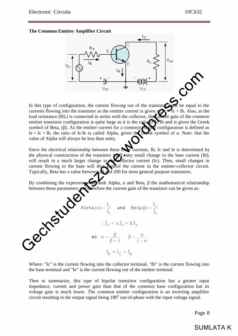
The Common Emitter Amplifier Circuit
In this type of configuration, the current flowing out of the transistor must be equal to the
currents flowing into the transistor as the emitter current is given as Ie = Ic + Ib. Also, as the
load resistance (RL) is connected in series with the collector, the current gain of the common
emitter transistor configuration is quite large as it is the ratio of Ic/Ib and is given the Greek
symbol of Beta, (β). As the emitter current for a common emitter configuration is defined as
Ie = Ic + Ib, the ratio of Ic/Ie is called Alpha, given the Greek symbol of α. Note: that the
value of Alpha will always be less than unity.
Since the electrical relationship between these three currents, Ib, Ic and Ie is determined by
the physical construction of the transistor itself, any small change in the base current (Ib),
will result in a much larger change in the collector current (Ic). Then, small changes in
current flowing in the base will thus control the current in the emitter-collector circuit.
Typically, Beta has a value between 20 and 200 for most general purpose transistors.
By combining the expressions for both Alpha, α and Beta, β the mathematical relationship
between these parameters and therefore the current gain of the transistor can be given as:
Where: "Ic" is the current flowing into the collector terminal, "Ib" is the current flowing into
the base terminal and "Ie" is the current flowing out of the emitter terminal.
Then to summarize, this type of bipolar transistor configuration has a greater input
impedance, current and power gain than that of the common base configuration but its
voltage gain is much lower. The common emitter configuration is an inverting amplifier
circuit resulting in the output signal being 180o out-of-phase with the input voltage signal.
Page 8
Gechs
tude
ntsz
one.
wordp
ress
.com
SUMLATA K
Electronic Circuits 10CS32
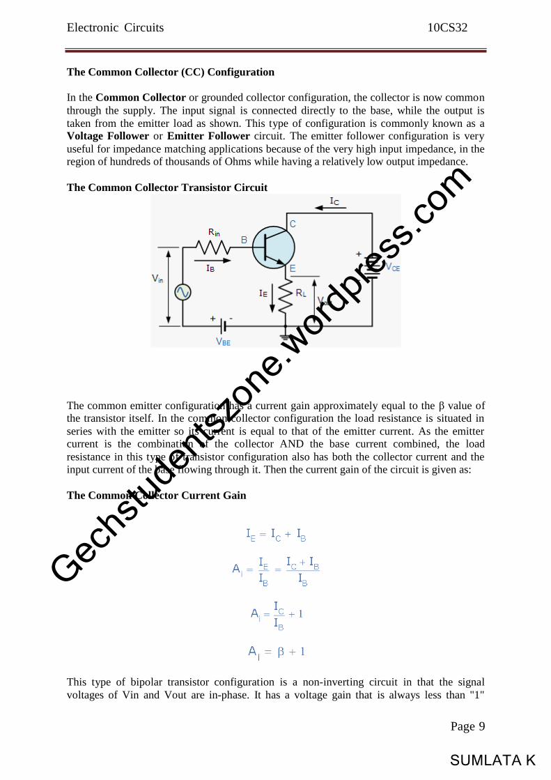
The Common Collector (CC) Configuration
In the Common Collector or grounded collector configuration, the collector is now common
through the supply. The input signal is connected directly to the base, while the output is
taken from the emitter load as shown. This type of configuration is commonly known as a Voltage Follower or Emitter Follower circuit. The emitter follower configuration is very
useful for impedance matching applications because of the very high input impedance, in the region of hundreds of thousands of Ohms while having a relatively low output impedance.
The Common Collector Transistor Circuit
The common emitter configuration has a current gain approximately equal to the β value of the transistor itself. In the common collector configuration the load resistance is situated in
series with the emitter so its current is equal to that of the emitter current. As the emitter current is the combination of the collector AND the base current combined, the load
resistance in this type of transistor configuration also has both the collector current and the
input current of the base flowing through it. Then the current gain of the circuit is given as:
The Common Collector Current Gain
This type of bipolar transistor configuration is a non-inverting circuit in that the signal
voltages of Vin and Vout are in-phase. It has a voltage gain that is always less than "1"
Page 9
Gechs
tude
ntsz
one.
wordp
ress
.com
SUMLATA K
Electronic Circuits 10CS32
(unity). The load resistance of the common collector transistor receives both the base and
collector currents giving a large current gain (as with the common emitter configuration)
therefore, providing good current amplification with very little voltage gain.
Bipolar Transistor Summary
Then to summarize, the behavior of the bipolar transistor in each one of the above circuit
configurations is very different and produces different circuit characteristics with regards to
input impedance, output impedance and gain whether this is voltage gain, current gain or
power gain and this is summarized in the table below.
Bipolar Transistor Characteristics
The static characteristics for a Bipolar Transistor can be divided into the following three
main groups.
Input Characteristics:- Common Base - ΔVEB / ΔIE
Common Emitter - ΔVBE / ΔIB
Output Characteristics:- Common Base - ΔVC / ΔIC
Common Emitter - ΔVC / ΔIC
Transfer Characteristics:- Common Base - ΔIC / ΔIE
Common Emitter - ΔIC / ΔIB
With the characteristics of the different transistor configurations given in the following table:
Common Common Common Base Emitter Collector
Low Medium High
Very High High Low
0o 180
o 0
o
High Medium Low
Low Medium High
Low Very High Medium
In the next tutorial about Bipolar Transistors, we will look at the NPN Transistor in more
detail when used in the common emitter configuration as an amplifier as this is the most
widely used configuration due to its flexibility and high gain. We will also plot the output
characteristics curves commonly associated with amplifier circuits as a function of the
collector current to the base current.
Page 10
Characteristic
Input Impedance
Output Impedance
Phase Angle
Voltage Gain
Current Gain
Power Gain
Gec
hstu
dent
szon
e.wor
dpre
ss.c
om
SUMLATA K
Electronic Circuits 10CS32
The NPN Transistor
In the previous tutorial we saw that the standard Bipolar Transistor or BJT, comes in two
basic forms. An NPN (Negative-Positive-Negative) type and a PNP (Positive-Negative-
Positive) type, with the most commonly used transistor type being the NPN Transistor. We also learnt that the transistor junctions can be biased in one of three different ways -
Common Base, Common Emitter and Common Collector. In this tutorial we will look more closely at the "Common Emitter" configuration using NPN Transistors with an
example of the construction of a NPN transistor along with the transistors current flow
characteristics is given below.
An NPN Transistor Configuration
(Note: Arrow defines the emitter and conventional current flow, "out" for an NPN transistor.)
The construction and terminal voltages for an NPN transistor are shown above. The voltage between the Base and Emitter ( VBE ), is positive at the Base and negative at the Emitter
because for an NPN transistor, the Base terminal is always positive with respect to the Emitter. Also the Collector supply voltage is positive with respect to the Emitter (VCE). So for
an NPN transistor to conduct the Collector is always more positive with respect to both the
Base and the Emitter.
NPN Transistor Connections
Then the voltage sources are connected to an NPN transistor as shown. The Collector is connected to the supply voltage VCC via the load resistor, RL which also acts to limit the
maximum current flowing through the device. The Base supply voltage VB is connected to
the Base resistor RB, which again is used to limit the maximum Base current.
We know that the transistor is a "current" operated device (Beta model) and that a large current ( Ic ) flows freely through the device between the collector and the emitter terminals
Page 11
Gec
hstu
dent
szon
e.wor
dpre
ss.c
om
SUMLATA K
Electronic Circuits 10CS32
when the transistor is switched "fully-ON". However, this only happens when a small biasing
current ( Ib ) is flowing into the base terminal of the transistor at the same time thus allowing
the Base to act as a sort of current control input.
The transistor current in an NPN transistor is the ratio of these two currents ( Ic/Ib ), called the DC Current Gain of the device and is given the symbol of hfe or nowadays Beta, ( β ).
The value of β can be large up to 200 for standard transistors, and it is this large ratio between Ic and Ib that makes the NPN transistor a useful amplifying device when used in its active
region as Ib provides the input and Ic provides the output. Note that Beta has no units as it is
a ratio.
Also, the current gain of the transistor from the Collector terminal to the Emitter terminal,
Ic/Ie, is called Alpha, ( α ), and is a function of the transistor itself (electrons diffusing across
the junction). As the emitter current Ie is the product of a very small base current plus a very
large collector current, the value of alpha α, is very close to unity, and for a typical low-
power signal transistor this value ranges from about 0.950 to 0.999
α and β Relationship in a NPN Transistor
By combining the two parameters α and β we can produce two mathematical expressions that
gives the relationship between the different currents flowing in the transistor.
The values of Beta vary from about 20 for high current power transistors to well over 1000
for high frequency low power type bipolar transistors. The value of Beta for most standard
NPN transistors can be found in the manufactures datasheets but generally range between 50 - 200.
The equation above for Beta can also be re-arranged to make Ic as the subject, and with a
zero base current ( Ib = 0 ) the resultant collector current Ic will also be zero, ( β x 0 ). Also when the base current is high the corresponding collector current will also be high resulting
Page 12
Gec
hstu
dent
szon
e.wor
dpre
ss.c
om
SUMLATA K
Electronic Circuits 10CS32
in the base current controlling the collector current. One of the most important properties of
the Bipolar Junction Transistor is that a small base current can control a much larger
collector current. Consider the following example.
Example No1
An NPN Transistor has a DC current gain, (Beta) value of 200. Calculate the base current Ib
required to switch a resistive load of 4mA.
Therefore, β = 200, Ic = 4mA and Ib = 20µA.
One other point to remember about NPN Transistors. The collector voltage, ( Vc ) must be
greater and positive with respect to the emitter voltage, ( Ve ) to allow current to flow
through the transistor between the collector-emitter junctions. Also, there is a voltage drop between the Base and the Emitter terminal of about 0.7v (one diode volt drop) for silicon
devices as the input characteristics of an NPN Transistor are of a forward biased diode. Then the base voltage, ( Vbe ) of a NPN transistor must be greater than this 0.7V otherwise the
transistor will not conduct with the base current given as.
Where: Ib is the base current, Vb is the base bias voltage, Vbe is the base-emitter volt drop
(0.7v) and Rb is the base input resistor. Increasing Ib, Vbe slowly increases to 0.7V but Ic
rises exponentially.
Example No2
An NPN Transistor has a DC base bias voltage, Vb of 10v and an input base resistor, Rb of
100kΩ. What will be the value of the base current into the transistor.
Therefore, Ib = 93µA.
The Common Emitter Configuration
As well as being used as a semiconductor switch to turn load currents "ON" or "OFF" by
controlling the Base signal to the transistor in ether its saturation or cut-off regions, NPN
Transistors can also be used in its active region to produce a circuit which will amplify any
small AC signal applied to its Base terminal with the Emitter grounded. If a suitable DC
"biasing" voltage is firstly applied to the transistors Base terminal thus allowing it to always
Page 13
Gec
hstu
dent
szon
e.wor
dpre
ss.c
om
SUMLATA K
Electronic Circuits 10CS32
operate within its linear active region, an inverting amplifier circuit called a single stage
common emitter amplifier is produced.
One such Common Emitter Amplifier configuration of an NPN transistor is called a Class A
Amplifier. A "Class A Amplifier" operation is one where the transistors Base terminal is biased in such a way as to forward bias the Base-emitter junction. The result is that the
transistor is always operating halfway between its cut-off and saturation regions, thereby allowing the transistor amplifier to accurately reproduce the positive and negative halves of
any AC input signal superimposed upon this DC biasing voltage. Without this "Bias Voltage"
only one half of the input waveform would be amplified. This common emitter amplifier
configuration using an NPN transistor has many applications but is commonly used in audio
circuits such as pre-amplifier and power amplifier stages.
With reference to the common emitter configuration shown below, a family of curves known
as the Output Characteristics Curves, relates the output collector current, (Ic) to the
collector voltage, (Vce) when different values of Base current, (Ib) are applied to the
transistor for transistors with the same β value. A DC "Load Line" can also be drawn onto the
output characteristics curves to show all the possible operating points when different values
of base current are applied. It is necessary to set the initial value of Vce correctly to allow the output voltage to vary both up and down when amplifying AC input signals and this is called
setting the operating point or Quiescent Point, Q-point for short and this is shown below.
Single Stage Common Emitter Amplifier Circuit
Page 14
Gec
hstu
dent
szon
e.wor
dpre
ss.c
om
SUMLATA K
Electronic Circuits 10CS32
Output Characteristics Curves of a Typical Bipolar Transistor
The most important factor to notice is the effect of Vce upon the collector current Ic when Vce is greater than about 1.0 volts. We can see that Ic is largely unaffected by changes in Vce
above this value and instead it is almost entirely controlled by the base current, Ib. When this happens we can say then that the output circuit represents that of a "Constant Current
Source". It can also be seen from the common emitter circuit above that the emitter current Ie is the sum of the collector current, Ic and the base current, Ib, added together so we can also
say that Ie = Ic + Ib for the common emitter (CE) configuration.
By using the output characteristics curves in our example above and also Ohm´s Law, the
current flowing through the load resistor, (RL), is equal to the collector current, Ic entering the transistor which inturn corresponds to the supply voltage, (Vcc) minus the voltage drop
between the collector and the emitter terminals, (Vce) and is given as:
Also, a straight line representing the Dynamic Load Line of the transistor can be drawn
directly onto the graph of curves above from the point of "Saturation" ( A ) when Vce = 0 to
the point of "Cut-off" ( B ) when Ic = 0 thus giving us the "Operating" or Q-point of the
transistor. These two points are joined together by a straight line and any position along this
straight line represents the "Active Region" of the transistor. The actual position of the load
line on the characteristics curves can be calculated as follows:
Page 15
Gec
hstu
dent
szon
e.wor
dpre
ss.c
om
SUMLATA K
Electronic Circuits 10CS32
Then, the collector or output characteristics curves for Common Emitter NPN Transistors
can be used to predict the Collector current, Ic, when given Vce and the Base current, Ib. A
Load Line can also be constructed onto the curves to determine a suitable Operating or Q-
point which can be set by adjustment of the base current. The slope of this load line is equal
to the reciprocal of the load resistance which is given as: -1/RL
Then we can define a NPN Transistor as being normally "OFF" but a small input current
and a small positive voltage at its Base (B) relative to its Emitter (E) will turn it "ON"
allowing a much large Collector-Emitter current to flow. NPN transistors conduct when Vc is
much greater than Ve.
In the next tutorial about Bipolar Transistors, we will look at the opposite or complementary form of the NPN Transistor called the PNP Transistor and show that the
PNP Transistor has very similar characteristics to their NPN transistor except that the
polarities (or biasing) of the current and voltage directions are reversed.
The PNP Transistor
The PNP Transistor is the exact opposite to the NPN Transistor device we looked at in the
previous tutorial. Basically, in this type of transistor construction the two diodes are reversed
with respect to the NPN type giving a Positive-Negative-Positive configuration, with the arrow which also defines the Emitter terminal this time pointing inwards in the transistor
symbol.
Also, all the polarities for a PNP transistor are reversed which means that it "sinks" current as
opposed to the NPN transistor which "sources" current. The main difference between the two
types of transistors is that holes are the more important carriers for PNP transistors, whereas electrons are the important carriers for NPN transistors. Then, PNP transistors use a small
output base current and a negative base voltage to control a much larger emitter-collector current. The construction of a PNP transistor consists of two P-type semiconductor materials
either side of the N-type material as shown below.
A PNP Transistor Configuration
Page 16
Gec
hstu
dent
szon
e.wor
dpre
ss.c
om
SUMLATA K
Electronic Circuits 10CS32
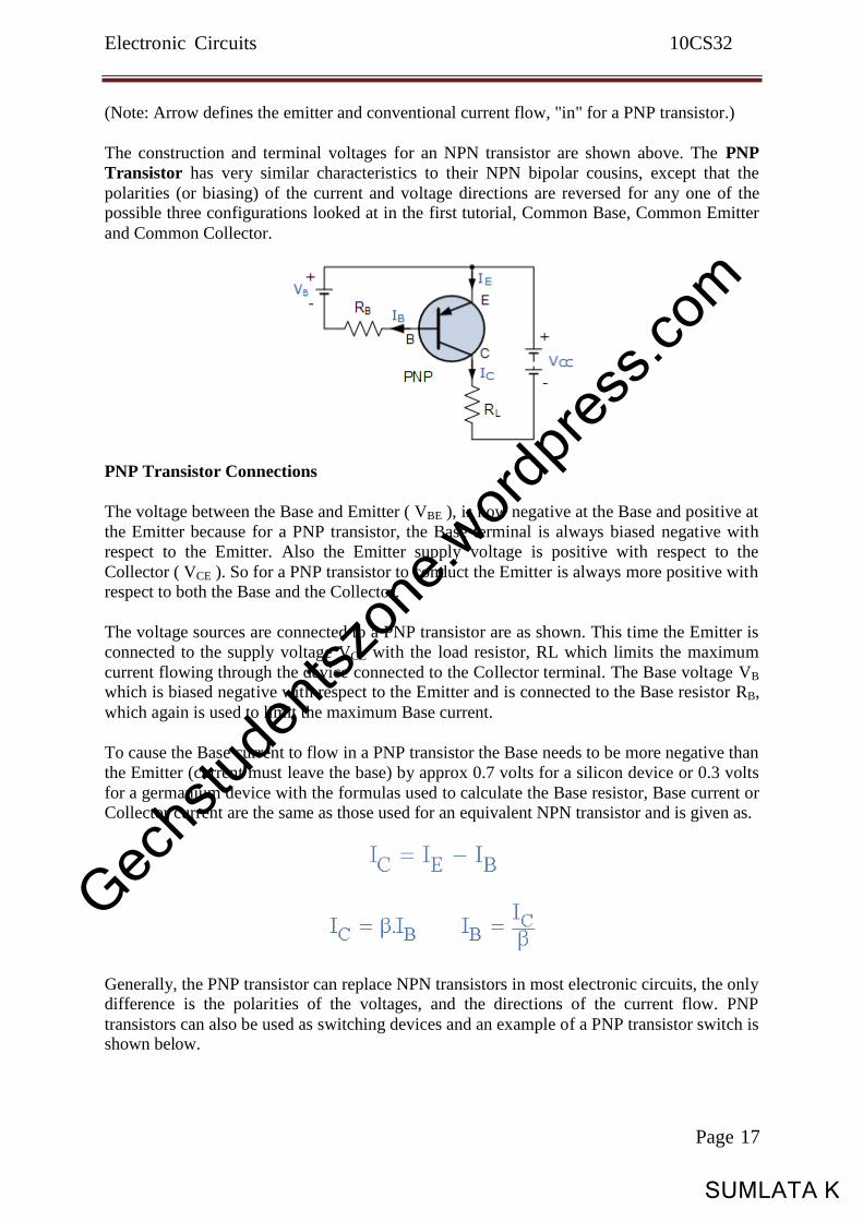
(Note: Arrow defines the emitter and conventional current flow, "in" for a PNP transistor.)
The construction and terminal voltages for an NPN transistor are shown above. The PNP
Transistor has very similar characteristics to their NPN bipolar cousins, except that the
polarities (or biasing) of the current and voltage directions are reversed for any one of the possible three configurations looked at in the first tutorial, Common Base, Common Emitter
and Common Collector.
PNP Transistor Connections
The voltage between the Base and Emitter ( VBE ), is now negative at the Base and positive at
the Emitter because for a PNP transistor, the Base terminal is always biased negative with
respect to the Emitter. Also the Emitter supply voltage is positive with respect to the
Collector ( VCE ). So for a PNP transistor to conduct the Emitter is always more positive with
respect to both the Base and the Collector.
The voltage sources are connected to a PNP transistor are as shown. This time the Emitter is
connected to the supply voltage VCC with the load resistor, RL which limits the maximum
current flowing through the device connected to the Collector terminal. The Base voltage VB
which is biased negative with respect to the Emitter and is connected to the Base resistor RB,
which again is used to limit the maximum Base current.
To cause the Base current to flow in a PNP transistor the Base needs to be more negative than
the Emitter (current must leave the base) by approx 0.7 volts for a silicon device or 0.3 volts
for a germanium device with the formulas used to calculate the Base resistor, Base current or
Collector current are the same as those used for an equivalent NPN transistor and is given as.
Generally, the PNP transistor can replace NPN transistors in most electronic circuits, the only difference is the polarities of the voltages, and the directions of the current flow. PNP
transistors can also be used as switching devices and an example of a PNP transistor switch is shown below.
Page 17
Gec
hstu
dent
szon
e.wor
dpre
ss.c
om
SUMLATA K
Electronic Circuits 10CS32
A PNP Transistor Circuit
The Output Characteristics Curves for a PNP transistor look very similar to those for an
equivalent NPN transistor except that they are rotated by 180o to take account of the reverse
polarity voltages and currents, (the currents flowing out of the Base and Collector in a PNP
transistor are negative). The same dynamic load line can be drawn onto the I-V curves to find
the PNP transistors operating points.
Transistor Matching
Page 18
Gec
hstu
dent
szon
e.wor
dpre
ss.c
om
SUMLATA K
Electronic Circuits 10CS32
Complementary Transistors
You may think what is the point of having a PNP Transistor, when there are plenty of NPN
Transistors available that can be used as an amplifier or solid-state switch?. Well, having two
different types of transistors "PNP" and "NPN", can be a great advantage when designing amplifier circuits such as the Class B Amplifier which uses "Complementary" or "Matched
Pair" transistors in its output stage or in reversible H-Bridge motor control circuits were we
want to control the flow of current evenly in both directions.
A pair of corresponding NPN and PNP transistors with near identical characteristics to each
other are called Complementary Transistors for example, a TIP3055 (NPN transistor) and
the TIP2955 (PNP transistor) are good examples of complementary or matched pair silicon
power transistors. They both have a DC current gain, Beta, ( Ic/Ib ) matched to within 10%
and high Collector current of about 15A making them ideal for general motor control or
robotic applications.
Also, class B amplifiers use complementary NPN and PNP in their power output stage
design. The NPN transistor conducts for only the positive half of the signal while the PNP transistor conducts for negative half of the signal. This allows the amplifier to drive the
required power through the load loudspeaker in both directions at the stated nominal impedance and power resulting in an output current which is likely to be in the order of
several amps shared evenly between the two complementary transistors.
Identifying the PNP Transistor
We saw in the first tutorial of this transistors section, that transistors are basically made up of
two Diodes connected together back-to-back. We can use this analogy to determine whether a
transistor is of the PNP type or NPN type by testing its Resistance between the three different
leads, Emitter, Base and Collector. By testing each pair of transistor leads in both directions
with a multimeter will result in six tests in total with the expected resistance values in Ohm's
given below.
1. Emitter-Base Terminals - The Emitter to Base should act like a normal diode and conduct
one way only.
2. Collector-Base Terminals - The Collector-Base junction should act like a normal diode and
conduct one way only.
3. Emitter-Collector Terminals - The Emitter-Collector should not conduct in either direction.
Transistor resistance values for a PNP transistor and a NPN transistor
Between Transistor Terminals PNP NPN
Collector Emitter RHIGH RHIGH
Collector Base RLOW RHIGH
Emitter Collector RHIGH RHIGH
Emitter Base RLOW RHIGH
Base Collector RHIGH RLOW
Page 19
Gec
hstu
dent
szon
e.wor
dpre
ss.c
om
SUMLATA K
Electronic Circuits 10CS32
Base Emitter RHIGH RLOW
Then we can define a PNP Transistor as being normally "OFF" but a small output current
and negative voltage at its Base (B) relative to its Emitter (E) will turn it "ON" allowing a much large Emitter-Collector current to flow. PNP transistors conduct when Ve is much
greater than Vc.
In the next tutorial about Bipolar Transistors instead of using the transistor as an amplifying
device, we will look at the operation of the transistor in its saturation and cut-off regions
when used as a solid-state switch. Bipolar transistor switches are used in many applications to
switch a DC current "ON" or "OFF" such as LED‟s which require only a few milliamps at
low DC voltages, or relays which require higher currents at higher voltages.
1.3 The Transistor as a Switch
When used as an AC signal amplifier, the transistors Base biasing voltage is applied in such a
way that it always operates within its "active" region, that is the linear part of the output
characteristics curves are used. However, both the NPN & PNP type bipolar transistors can
be made to operate as "ON/OFF" type solid state switches by biasing the transistors base
differently to that of a signal amplifier. Solid state switches are one of the main applications
for the use of transistors, and transistor switches can be used for controlling high power
devices such as motors, solenoids or lamps, but they can also used in digital electronics and
logic gate circuits.
If the circuit uses the Bipolar Transistor as a Switch, then the biasing of the transistor,
either NPN or PNP is arranged to operate the transistor at both sides of the I-V characteristics curves we have seen previously. The areas of operation for a transistor switch are known as
the Saturation Region and the Cut-off Region. This means then that we can ignore the operating Q-point biasing and voltage divider circuitry required for amplification, and use the
transistor as a switch by driving it back and forth between its "fully-OFF" (cut-off) and
"fully-ON" (saturation) regions as shown below.
Basic NPN Transistor Switching Circuit
The circuit resembles that of the Common Emitter circuit we looked at in the previous
tutorials. The difference this time is that to operate the transistor as a switch the transistor needs to be turned either fully "OFF" (cut-off) or fully "ON" (saturated). An ideal transistor
switch would have infinite circuit resistance between the Collector and Emitter when turned
Page 20
Gec
hstu
dent
szon
e.wor
dpre
ss.c
om
SUMLATA K
Electronic Circuits 10CS32
"fully-OFF" resulting in zero current flowing through it and zero resistance between the
Collector and Emitter when turned "fully-ON", resulting in maximum current flow. In
practice when the transistor is turned "OFF", small leakage currents flow through the
transistor and when fully "ON" the device has a low resistance value causing a small
saturation voltage (VCE) across it. Even though the transistor is not a perfect switch, in both
the cut-off and saturation regions the power dissipated by the transistor is at its minimum.
In order for the Base current to flow, the Base input terminal must be made more positive
than the Emitter by increasing it above the 0.7 volts needed for a silicon device. By varying
this Base-Emitter voltage VBE, the Base current is also altered and which in turn controls the
amount of Collector current flowing through the transistor as previously discussed. When
maximum Collector current flows the transistor is said to be Saturated. The value of the
Base resistor determines how much input voltage is required and corresponding Base current
to switch the transistor fully "ON".
Example No1
Using the transistor values from the previous tutorials of: β = 200, Ic = 4mA and Ib = 20uA, find the value of the Base resistor (Rb) required to switch the load "ON" when the input
terminal voltage exceeds 2.5v.
The next lowest preferred value is: 82kΩ, this guarantees the transistor switch is always
saturated.
Example No2
Again using the same values, find the minimum Base current required to turn the transistor
"fully-ON" (saturated) for a load that requires 200mA of current when the input voltage is
increased to 5.0V. Also calculate the new value of Rb.
Transistor Base current:
Transistor Base resistance:
Transistor switches are used for a wide variety of applications such as interfacing large
current or high voltage devices like motors, relays or lamps to low voltage digital logic IC's
or gates like AND gates or OR gates. Here, the output from a digital logic gate is only +5v
but the device to be controlled may require a 12 or even 24 volts supply. Or the load such as a
Page 21
Gec
hstu
dent
szon
e.wor
dpre
ss.c
om
SUMLATA K
Electronic Circuits 10CS32
DC Motor may need to have its speed controlled using a series of pulses (Pulse Width
Modulation). Transistor switches will allow us to do this faster and more easily than with
conventional mechanical switches.
Digital Logic Transistor Switch
The base resistor, Rb is required to limit the output current from the logic gate.
PNP Transistor Switch
We can also use PNP transistors as switches, the difference this time is that the load is
connected to ground (0v) and the PNP transistor switches power to it. To turn the PNP transistor as a switch "ON" the Base terminal is connected to ground or zero volts (LOW) as
shown.
PNP Transistor Switching Circuit
The equations for calculating the Base resistance, Collector current and voltages are exactly
the same as for the previous NPN transistor switch. The difference this time is that we are
switching power with a PNP transistor (sourcing current) instead of switching ground with an
NPN transistor (sinking current).
Page 22
Gec
hstu
dent
szon
e.wor
dpre
ss.c
om
SUMLATA K
Electronic Circuits 10CS32
Unijunction transistor
Although a unijunction transistor is not a thyristor, this device can trigger larger thyristors
with a pulse at base B1. A unijunction transistor is composed of a bar of N-type silicon
having a P-type connection in the middle. See Figure below(a). The connections at the ends of the bar are known as bases B1 and B2; the P-type mid-point is the emitter. With the
emitter disconnected, the total resistance RBBO, a datasheet item, is the sum of RB1 and RB2 as shown in Figure below(b). RBBO ranges from 4-12kΩ for different device types. The
intrinsic standoff ratio η is the ratio of RB1 to RBBO. It varies from 0.4 to 0.8 for different
devices. The schematic symbol is Figure below(c)
Unijunction transistor: (a) Construction, (b) Model, (c) Symbol
The Unijunction emitter current vs voltage characteristic curve (Figure below(a) ) shows that
as VE increases, current IE increases up IP at the peak point. Beyond the peak point, current increases as voltage decreases in the negative resistance region. The voltage reaches a
minimum at the valley point. The resistance of RB1, the saturation resistance is lowest at the
valley point.
IP and IV, are datasheet parameters; For a 2n2647, IP and IV are 2µA and 4mA, respectively.
[AMS] VP is the voltage drop across RB1 plus a 0.7V diode drop; see Figure below(b). VV
is estimated to be approximately 10% of VBB.
Unijunction transistor: (a) emitter characteristic curve, (b) model for VP .
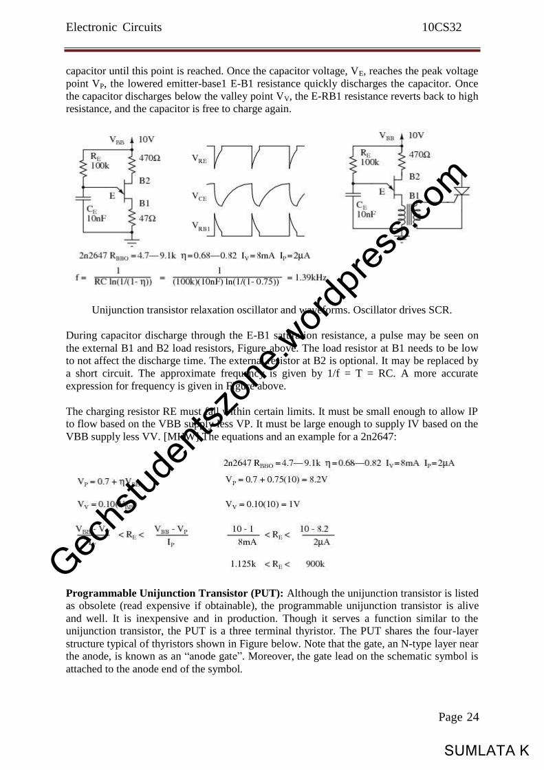
The relaxation oscillator in Figure below is an application of the unijunction oscillator. RE
charges CE until the peak point. The unijunction emitter terminal has no effect on the
Page 23
Gec
hstu
dent
szon
e.wor
dpre
ss.c
om
SUMLATA K
Electronic Circuits 10CS32
capacitor until this point is reached. Once the capacitor voltage, VE, reaches the peak voltage
point VP, the lowered emitter-base1 E-B1 resistance quickly discharges the capacitor. Once
the capacitor discharges below the valley point VV, the E-RB1 resistance reverts back to high
resistance, and the capacitor is free to charge again.
Unijunction transistor relaxation oscillator and waveforms. Oscillator drives SCR.
During capacitor discharge through the E-B1 saturation resistance, a pulse may be seen on
the external B1 and B2 load resistors, Figure above. The load resistor at B1 needs to be low
to not affect the discharge time. The external resistor at B2 is optional. It may be replaced by
a short circuit. The approximate frequency is given by 1/f = T = RC. A more accurate
expression for frequency is given in Figure above.
The charging resistor RE must fall within certain limits. It must be small enough to allow IP to flow based on the VBB supply less VP. It must be large enough to supply IV based on the
VBB supply less VV. [MHW] The equations and an example for a 2n2647:
Programmable Unijunction Transistor (PUT): Although the unijunction transistor is listed as obsolete (read expensive if obtainable), the programmable unijunction transistor is alive
and well. It is inexpensive and in production. Though it serves a function similar to the unijunction transistor, the PUT is a three terminal thyristor. The PUT shares the four-layer
structure typical of thyristors shown in Figure below. Note that the gate, an N-type layer near the anode, is known as an “anode gate”. Moreover, the gate lead on the schematic symbol is
The characteristic curve for the programmable unijunction transistor in Figure above is
similar to that of the unijunction transistor. This is a plot of anode current IA versus anode
voltage VA. The gate lead voltage sets, programs, the peak anode voltage VP. As anode
current inceases, voltage increases up to the peak point. Thereafter, increasing current results
in decreasing voltage, down to the valley point.
The PUT equivalent of the unijunction transistor is shown in Figure below. External PUT resistors R1 and R2 replace unijunction transistor internal resistors RB1 and RB2, respectively.
These resistors allow the calculation of the intrinsic standoff ratio η.
PUT equivalent of unijunction transistor
Figure below shows the PUT version of the unijunction relaxation oscillator Figure previous.
Resistor R charges the capacitor until the peak point, Figure previous, then heavy conduction
moves the operating point down the negative resistance slope to the valley point. A current
spike flows through the cathode during capacitor discharge, developing a voltage spike across
the cathode resistors. After capacitor discharge, the operating point resets back to the slope up to the peak point.
Page 25
Gec
hstu
dent
szon
e.wor
dpre
ss.c
om
SUMLATA K
Electronic Circuits 10CS32
PUT relaxation oscillator
Problem: What is the range of suitable values for R in Figure above, a relaxation oscillator?
The charging resistor must be small enough to supply enough current to raise the anode to VP
the peak point (Figure previous) while charging the capacitor. Once VP is reached, anode
voltage decreases as current increases (negative resistance), which moves the operating point
to the valley. It is the job of the capacitor to supply the valley current IV. Once it is
discharged, the operating point resets back to the upward slope to the peak point. The resistor
must be large enough so that it will never supply the high valley current IP. If the charging
resistor ever could supply that much current, the resistor would supply the valley current after
the capacitor was discharged and the operating point would never reset back to the high
resistance condition to the left of the peak point.
We select the same VBB=10V used for the unijunction transistor example. We select values
of R1 and R2 so that η is about 2/3. We calculate η and VS. The parallel equivalent of R1, R2 is RG, which is only used to make selections from Table below. Along with VS=10, the
closest value to our 6.3, we find VT=0.6V, in Table below and calculate VP.
We also find IP and IV, the peak and valley currents, respectively in Table below. We still
need VV, the valley voltage. We used 10% of VBB= 1V, in the previous unijunction
example. Consulting the datasheet, we find the forward voltage VF=0.8V at IF=50mA. The
valley current IV=70µA is much less than IF=50mA. Therefore, VV must be less than
VF=0.8V. How much less? To be safe we set VV=0V. This will raise the lower limit on the
resistor range a little.
Page 26
Gec
hstu
dent
szon
e.wor
dpre
ss.c
om
SUMLATA K
Electronic Circuits 10CS32
Choosing R > 143k guarantees that the operating point can reset from the valley point after
capacitor discharge. R < 755k allows charging up to VP at the peak point.
Figure below show the PUT relaxation oscillator with the final resistor values. A practical
application of a PUT triggering an SCR is also shown. This circuit needs a VBB unfiltered
supply (not shown) divided down from the bridge rectifier to reset the relaxation oscillator
after each power zero crossing. The variable resistor should have a minimum resistor in series
with it to prevent a low pot setting from hanging at the valley point.
PUT relaxation oscillator with component values. PUT drives SCR lamp dimmer.
1.4 Silicon-Controlled Rectifiers, or SCRs
Shockley diodes are curious devices, but rather limited in application. Their usefulness may be expanded, however, by equipping them with another means of latching. In doing so, each
becomes true amplifying devices (if only in an on/off mode), and we refer to these as silicon-
controlled rectifiers, or SCRs.
The progression from Shockley diode to SCR is achieved with one small addition, actually
nothing more than a third wire connection to the existing PNPN structure: (Figure below)
Page 27
Gec
hstu
dent
szon
e.wor
dpre
ss.c
om
SUMLATA K
Electronic Circuits 10CS32
The Silicon-Controlled Rectifier (SCR)
If an SCR's gate is left floating (disconnected), it behaves exactly as a Shockley diode. It may
be latched by break-over voltage or by exceeding the critical rate of voltage rise between
anode and cathode, just as with the Shockley diode. Dropout is accomplished by reducing current until one or both internal transistors fall into cutoff mode, also like the Shockley
diode. However, because the gate terminal connects directly to the base of the lower transistor, it may be used as an alternative means to latch the SCR. By applying a small
voltage between gate and cathode, the lower transistor will be forced on by the resulting base
current, which will cause the upper transistor to conduct, which then supplies the lower
transistor's base with current so that it no longer needs to be activated by a gate voltage. The
necessary gate current to initiate latch-up, of course, will be much lower than the current
through the SCR from cathode to anode, so the SCR does achieve a measure of amplification.
This method of securing SCR conduction is called triggering, and it is by far the most
common way that SCRs are latched in actual practice. In fact, SCRs are usually chosen so
that their breakover voltage is far beyond the greatest voltage expected to be experienced
from the power source, so that it can be turned on only by an intentional voltage pulse applied
to the gate.
It should be mentioned that SCRs may sometimes be turned off by directly shorting their gate
and cathode terminals together, or by "reverse-triggering" the gate with a negative voltage (in
reference to the cathode), so that the lower transistor is forced into cutoff. I say this is
"sometimes" possible because it involves shunting all of the upper transistor's collector
current past the lower transistor's base. This current may be substantial, making triggered
shut-off of an SCR difficult at best. A variation of the SCR, called a Gate-Turn-Off thyristor,
or GTO, makes this task easier. But even with a GTO, the gate current required to turn it off
may be as much as 20% of the anode (load) current! The schematic symbol for a GTO is
shown in the following illustration: (Figure below)
1.5 The Gate Turn-Off Thyristors (GTO)
SCRs and GTOs share the same equivalent schematics (two transistors connected in a positive-feedback fashion), the only differences being details of construction designed to
grant the NPN transistor a greater β than the PNP. This allows a smaller gate current (forward
or reverse) to exert a greater degree of control over conduction from cathode to anode, with
the PNP transistor's latched state being more dependent upon the NPN's than vice versa. The
Gate-Turn-Off thyristor is also known by the name of Gate-Controlled Switch, or GCS.
A rudimentary test of SCR function, or at least terminal identification, may be performed
with an ohmmeter. Because the internal connection between gate and cathode is a single PN
junction, a meter should indicate continuity between these terminals with the red test lead on
the gate and the black test lead on the cathode like this: (Figure below)
Page 28
Gec
hstu
dent
szon
e.wor
dpre
ss.c
om
SUMLATA K
Electronic Circuits 10CS32
Rudimentary test of SCR
All other continuity measurements performed on an SCR will show "open" ("OL" on some
digital multimeter displays). It must be understood that this test is very crude and does not
constitute a comprehensive assessment of the SCR. It is possible for an SCR to give good
ohmmeter indications and still be defective. Ultimately, the only way to test an SCR is to
subject it to a load current.
If you are using a multimeter with a "diode check" function, the gate-to-cathode junction
voltage indication you get may or may not correspond to what's expected of a silicon PN junction (approximately 0.7 volts). In some cases, you will read a much lower junction
voltage: mere hundredths of a volt. This is due to an internal resistor connected between the gate and cathode incorporated within some SCRs. This resistor is added to make the SCR less
susceptible to false triggering by spurious voltage spikes, from circuit "noise" or from static electric discharge. In other words, having a resistor connected across the gate-cathode
junction requires that a strong triggering signal (substantial current) be applied to latch the SCR. This feature is often found in larger SCRs, not on small SCRs. Bear in mind that an
SCR with an internal resistor connected between gate and cathode will indicate continuity in both directions between those two terminals: (Figure below)
Larger SCRs have gate to cathode resistor.
"Normal" SCRs, lacking this internal resistor, are sometimes referred to as sensitive gate
SCRs due to their ability to be triggered by the slightest positive gate signal.
The test circuit for an SCR is both practical as a diagnostic tool for checking suspected SCRs and also an excellent aid to understanding basic SCR operation. A DC voltage source is used
Page 29
Gec
hstu
dent
szon
e.wor
dpre
ss.c
om
SUMLATA K
Electronic Circuits 10CS32
for powering the circuit, and two pushbutton switches are used to latch and unlatch the SCR,
respectively: (Figure below)
SCR testing circuit
Actuating the normally-open "on" pushbutton switch connects the gate to the anode, allowing current from the negative terminal of the battery, through the cathode-gate PN junction,
through the switch, through the load resistor, and back to the battery. This gate current should force the SCR to latch on, allowing current to go directly from cathode to anode without
further triggering through the gate. When the "on" pushbutton is released, the load should
remain energized.
Pushing the normally-closed "off" pushbutton switch breaks the circuit, forcing current
through the SCR to halt, thus forcing it to turn off (low-current dropout).
If the SCR fails to latch, the problem may be with the load and not the SCR. A certain minimum amount of load current is required to hold the SCR latched in the "on" state. This
minimum current level is called the holding current. A load with too great a resistance value
may not draw enough current to keep an SCR latched when gate current ceases, thus giving
the false impression of a bad (unlatchable) SCR in the test circuit. Holding current values for
different SCRs should be available from the manufacturers. Typical holding current values
range from 1 milliamp to 50 milliamps or more for larger units.
For the test to be fully comprehensive, more than the triggering action needs to be tested. The
forward breakover voltage limit of the SCR could be tested by increasing the DC voltage
supply (with no pushbuttons actuated) until the SCR latches all on its own. Beware that a
breakover test may require very high voltage: many power SCRs have breakover voltage
ratings of 600 volts or more! Also, if a pulse voltage generator is available, the critical rate of
voltage rise for the SCR could be tested in the same way: subject it to pulsing supply voltages
of different V/time rates with no pushbutton switches actuated and see when it latches.
In this simple form, the SCR test circuit could suffice as a start/stop control circuit for a DC
motor, lamp, or other practical load: (Figure below)
Page 30
Gec
hstu
dent
szon
e.wor
dpre
ss.c
om
SUMLATA K
Electronic Circuits 10CS32
DC motor start/stop control circuit
Another practical use for the SCR in a DC circuit is as a crowbar device for overvoltage
protection. A "crowbar" circuit consists of an SCR placed in parallel with the output of a DC
power supply, for placing a direct short-circuit on the output of that supply to prevent
excessive voltage from reaching the load. Damage to the SCR and power supply is prevented
by the judicious placement of a fuse or substantial series resistance ahead of the SCR to limit
short-circuit current: (Figure below)
Crowbar circuit used in DC power supply
Some device or circuit sensing the output voltage will be connected to the gate of the SCR, so
that when an overvoltage condition occurs, voltage will be applied between the gate and cathode, triggering the SCR and forcing the fuse to blow. The effect will be approximately
the same as dropping a solid steel crowbar directly across the output terminals of the power
supply, hence the name of the circuit.
Most applications of the SCR are for AC power control, despite the fact that SCRs are inherently DC (unidirectional) devices. If bidirectional circuit current is required, multiple
SCRs may be used, with one or more facing each direction to handle current through both
half-cycles of the AC wave. The primary reason SCRs are used at all for AC power control
applications is the unique response of a thyristor to an alternating current. As we saw, the
thyratron tube (the electron tube version of the SCR) and the DIAC, a hysteretic device
triggered on during a portion of an AC half-cycle will latch and remain on throughout the
remainder of the half-cycle until the AC current decreases to zero, as it must to begin the next
half-cycle. Just prior to the zero-crossover point of the current waveform, the thyristor will
turn off due to insufficient current (this behavior is also known as natural commutation) and
must be fired again during the next cycle. The result is a circuit current equivalent to a "chopped up" sine wave. For review, here is the graph of a DIAC's response to an AC voltage
whose peak exceeds the breakover voltage of the DIAC: (Figure below)
Page 31
Gec
hstu
dent
szon
e.wor
dpre
ss.c
om
SUMLATA K
Electronic Circuits 10CS32
DIAC bidirectional response
With the DIAC, that breakover voltage limit was a fixed quantity. With the SCR, we have
control over exactly when the device becomes latched by triggering the gate at any point in
time along the waveform. By connecting a suitable control circuit to the gate of an SCR, we
can "chop" the sine wave at any point to allow for time-proportioned power control to a load.
Take the circuit in Figure below as an example. Here, an SCR is positioned in a circuit to
control power to a load from an AC source.
SCR control of AC power
Being a unidirectional (one-way) device, at most we can only deliver half-wave power to the
load, in the half-cycle of AC where the supply voltage polarity is positive on the top and
negative on the bottom. However, for demonstrating the basic concept of time-proportional control, this simple circuit is better than one controlling full-wave power (which would
require two SCRs).
With no triggering to the gate, and the AC source voltage well below the SCR's breakover
voltage rating, the SCR will never turn on. Connecting the SCR gate to the anode through a
standard rectifying diode (to prevent reverse current through the gate in the event of the SCR
containing a built-in gate-cathode resistor), will allow the SCR to be triggered almost
immediately at the beginning of every positive half-cycle: (Figure below)
Gate connected directly to anode through a diode; nearly complete half-wave current through
load.
Page 32
Gec
hstu
dent
szon
e.wor
dpre
ss.c
om
SUMLATA K
Electronic Circuits 10CS32
We can delay the triggering of the SCR, however, by inserting some resistance into the gate
circuit, thus increasing the amount of voltage drop required before enough gate current
triggers the SCR. In other words, if we make it harder for electrons to flow through the gate
by adding a resistance, the AC voltage will have to reach a higher point in its cycle before
there will be enough gate current to turn the SCR on. The result is in Figure below.
Resistance inserted in gate circuit; less than half-wave current through load.
With the half-sine wave chopped up to a greater degree by delayed triggering of the SCR, the load receives less average power (power is delivered for less time throughout a cycle). By
making the series gate resistor variable, we can make adjustments to the time-proportioned
power: (Figure below)
Increasing the resistance raises the threshold level, causing less power to be delivered to the
load. Decreasing the resistance lowers the threshold level, causing more power to be
delivered to the load.
Unfortunately, this control scheme has a significant limitation. In using the AC source
waveform for our SCR triggering signal, we limit control to the first half of the waveform's
half-cycle. In other words, it is not possible for us to wait until after the wave's peak to trigger
the SCR. This means we can turn down the power only to the point where the SCR turns on
at the very peak of the wave: (Figure below)
Page 33
Gec
hstu
dent
szon
e.wor
dpre
ss.c
om
SUMLATA K
Electronic Circuits 10CS32
Circuit at minimum power setting
Raising the trigger threshold any more will cause the circuit to not trigger at all, since not
even the peak of the AC power voltage will be enough to trigger the SCR. The result will be
no power to the load.
An ingenious solution to this control dilemma is found in the addition of a phase-shifting
capacitor to the circuit: (Figure below)
Addition of a phase-shifting capacitor to the circuit
The smaller waveform shown on the graph is voltage across the capacitor. For the sake of illustrating the phase shift, I'm assuming a condition of maximum control resistance where
the SCR is not triggering at all with no load current, save for what little current goes through the control resistor and capacitor. This capacitor voltage will be phase-shifted anywhere from
0o to 90
o lagging behind the power source AC waveform. When this phase-shifted voltage
reaches a high enough level, the SCR will trigger.
With enough voltage across the capacitor to periodically trigger the SCR, the resulting load
current waveform will look something like Figure below)
Phase-shifted signal triggers SCR into conduction.
IT Page 34
Gec
hstu
dent
szon
e.wor
dpre
ss.c
om
SUMLATA K
Electronic Circuits 10CS32
Because the capacitor waveform is still rising after the main AC power waveform has
reached its peak, it becomes possible to trigger the SCR at a threshold level beyond that peak,
thus chopping the load current wave further than it was possible with the simpler circuit. In
reality, the capacitor voltage waveform is a bit more complex that what is shown here, its
sinusoidal shape distorted every time the SCR latches on. However, what I'm trying to illustrate here is the delayed triggering action gained with the phase-shifting RC network;
thus, a simplified, undistorted waveform serves the purpose well.
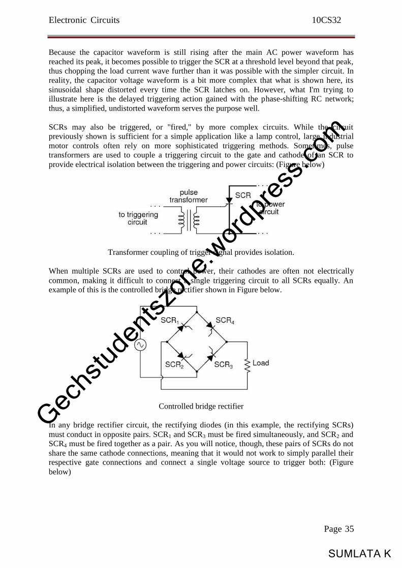
SCRs may also be triggered, or "fired," by more complex circuits. While the circuit
previously shown is sufficient for a simple application like a lamp control, large industrial
motor controls often rely on more sophisticated triggering methods. Sometimes, pulse
transformers are used to couple a triggering circuit to the gate and cathode of an SCR to
provide electrical isolation between the triggering and power circuits: (Figure below)
Transformer coupling of trigger signal provides isolation.
When multiple SCRs are used to control power, their cathodes are often not electrically
common, making it difficult to connect a single triggering circuit to all SCRs equally. An
example of this is the controlled bridge rectifier shown in Figure below.
Controlled bridge rectifier
In any bridge rectifier circuit, the rectifying diodes (in this example, the rectifying SCRs)
must conduct in opposite pairs. SCR1 and SCR3 must be fired simultaneously, and SCR2 and
SCR4 must be fired together as a pair. As you will notice, though, these pairs of SCRs do not
share the same cathode connections, meaning that it would not work to simply parallel their
respective gate connections and connect a single voltage source to trigger both: (Figure
below)
Page 35
Gec
hstu
dent
szon
e.wor
dpre
ss.c
om
SUMLATA K
Electronic Circuits 10CS32
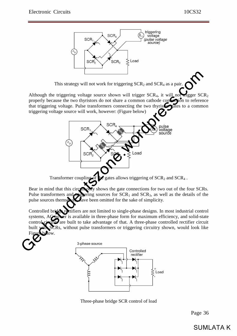
This strategy will not work for triggering SCR2 and SCR4 as a pair.
Although the triggering voltage source shown will trigger SCR4, it will not trigger SCR2
properly because the two thyristors do not share a common cathode connection to reference
that triggering voltage. Pulse transformers connecting the two thyristor gates to a common
triggering voltage source will work, however: (Figure below)
Transformer coupling of the gates allows triggering of SCR2 and SCR4 .
Bear in mind that this circuit only shows the gate connections for two out of the four SCRs.
Pulse transformers and triggering sources for SCR1 and SCR3, as well as the details of the
pulse sources themselves, have been omitted for the sake of simplicity.
Controlled bridge rectifiers are not limited to single-phase designs. In most industrial control
systems, AC power is available in three-phase form for maximum efficiency, and solid-state
control circuits are built to take advantage of that. A three-phase controlled rectifier circuit built with SCRs, without pulse transformers or triggering circuitry shown, would look like
Figure below.
Three-phase bridge SCR control of load
Page 36
Gec
hstu
dent
szon
e.wor
dpre
ss.c
om
SUMLATA K
Electronic Circuits 10CS32
1.6 Recommended Questions
1. Explain the clipping above and below the reference voltage in a basic parallel clipper. 2. Explain the clipping above and below the reference voltage in the basic series clipper.
3. Explain the clippers with voltage divider circuit.
4. Explain the negative & positive clamper circuit.
5. Draw and explain the characteristics of Schottky diode.
6. What is feature of a Varactor diode?
7. What is a voltage multiplier circuit? Explain the operation of a full wave voltage
doubler circuit. (Jan-2007)
8. Define diffusion capacitance. Derive an expression for the same. (July-2007)
9. Draw the piece wise linear V-I characteristics of a P-N junction diode. Give the
circuit model for the ON state and OFF state. (July-2007) 10. Discuss voltage doubler circuit. (Jan-2008)
11. Define regulation and derive equation for a full wave circuit. (Jan-2008)