United States Patent [191 Nozik 4,094,751 June 13, 1978 [11] [45] [54] PHOTOCHEMICAL DIODES [75] Inventor: Arthur J. Nozik, Summit, NJ. [73] Assignee: Allied Chemical Corporation, Morris Township, NJ. [21] Appl. No.: 728,474 [22] Filed: Sep. 30, 1976 [51] Int. Cl.2 ......................... .. C2513 1/00; C25B V04 [52] U.S. C1. ...................................... .. 204/80; 60/641; 204/84; 204/ 128; 204/ 129; 204/ 157.1 R; 204/248; 250/527; 357/85; 429/111 [58] Field of Search ................. .. 204/80, 84, 128, 129, 204/ 157.1 R, 248; 250/527; 429/111; 357/87, 85; 60/641; 136/203, 205, 206, 89 [56] References Cited U.S. PATENT DOCUMENTS 3,650,844 3/ 1972 Kendall, Jr. et al. .............. .. 136/237 3,914,856 10/1975 3,924,139 12/ 1975 3,925,212 12/1975 3,956,017 5/1976 3,961,997 6/1976 3,975,211 8/1976 4,011,149 3/1977 .. 4,021,323 5/1977 Kilby et a1. ........................ .. 204/ 129 OTHER PUBLICATIONS F. Shabkhan “The Effect of Illumination on the Anodic Dissolution of Cadmium Sulphide in the Presence of a Redox System,”Ber. Bunsen Phys. Chem., vol. 76, pp. 389-393 (1972). T. L. Chu et a1. “Polycrystalline Silicon Solar Cells on Low Cost Foreign Substrates”, Solar Energy, vol. 17, pp. 229—235 (1975). T. Saitoh et al. “Growth & Structure of Polycrystalline In P Layers on Molybdenum Sheets”, J. Electrochem. Soc., vol. 123, pp. 403-406, (Mar. 1976). P. H. Fang et a1. “Polycrystalline Silicon Films on Alu minum Sheets for Solar Cell Application,” Appl. Phys. Lett. vol. 25, pp. 1583-584 (1974). Semiconductor Electrodes Coated with Thin Metal Films,”Chemistry Letters, pp. 883-886 (1975). A. J. Nozik, “p-n Photoelectrolysis Cells,”App. Phys. Lett., vol. 29, pp. 150-153 (1976). A. J. Nozik, “Photoelectrolysis of Water Using Semi conducting TiOz Crystals,” Nature, vol. 257, pp. 383-386 (1975). L. L. Vant-Hull et a]. “Solar Thermal Power System Based on Optical Transmission,” Solar Energy, vol. 18, pp. 31-39 (1976). T. Wolkenstein, “The Electronic Theory of Photocata lytic Reactions on Semiconductors,” pp. 157-208 of Advances in Catalysis, vol. 23, Academic Press, NY. (1974). Primary Examiner—Aaron Weisstuch Attorney, Agent, or Firm—David W. Collins; Gerhard H. Fuchs [s7] ABSTRACI‘ Photochemical diodes are provided which use light to drive both endoergic and exoergic chemical reactions such that optical energy is converted into chemical energy. The photochemical diodes are typically sus pended in a bulk volume matrix of the constituent chemical reactants. The photochemical diodes, in the form of either Schottky-type diodes or p-n type diodes, are employed, for example, to convert water into hy drogen plus oxygen (or hydrogen peroxide); to convert hydrogen sul?de into hydrogen plus sulfur; and to photo-catalyze chemical reactions. The photochemical diodes of the invention comprise two portions, a ?rst portion comprising an appropriately doped semicon ductor material of a given conductivity and provided with an ohmic contact and a second portion comprising either metal (Schottky-type) or an appropriately doped semiconductor material of a conductivity type opposite to that of the ?rst portion and provided with an ohmic contact (p-n type). The two portions are intimately joined together through the ohmic contact(s). Solar radiation is conveniently employed as a source of opti cal energy. Y. Nakato et a1. “Photoelectrochemical Behaviours of 40 Claims, 9 Drawing Figures pqY-PE cgnHrnglgrs SEMICONDUCTOR 6' Z‘! REACTANT L32 3, "'TYPE REACTANT MATRIX -' sEmcoggucTon MATRIX 5’ - Q e-<— A*+e'-’A _ Ufb (n) -- -- -- 'Z'----- --FERMI LEVEL E --> h''' 24/ B'+ h"->B a7 h+ /-25
Transcript
United States Patent [191 Nozik
4,094,751 June 13, 1978
[11]
[45]
[54] PHOTOCHEMICAL DIODES
[75] Inventor: Arthur J. Nozik, Summit, NJ. [73] Assignee: Allied Chemical Corporation, Morris
F. Shabkhan “The Effect of Illumination on the Anodic Dissolution of Cadmium Sulphide in the Presence of a Redox System,”Ber. Bunsen Phys. Chem., vol. 76, pp. 389-393 (1972). T. L. Chu et a1. “Polycrystalline Silicon Solar Cells on Low Cost Foreign Substrates”, Solar Energy, vol. 17, pp. 229—235 (1975). T. Saitoh et al. “Growth & Structure of Polycrystalline In P Layers on Molybdenum Sheets”, J. Electrochem. Soc., vol. 123, pp. 403-406, (Mar. 1976). P. H. Fang et a1. “Polycrystalline Silicon Films on Alu minum Sheets for Solar Cell Application,” Appl. Phys. Lett. vol. 25, pp. 1583-584 (1974).
Semiconductor Electrodes Coated with Thin Metal Films,”Chemistry Letters, pp. 883-886 (1975). A. J. Nozik, “p-n Photoelectrolysis Cells,”App. Phys. Lett., vol. 29, pp. 150-153 (1976). A. J. Nozik, “Photoelectrolysis of Water Using Semi conducting TiOz Crystals,” Nature, vol. 257, pp. 383-386 (1975). L. L. Vant-Hull et a]. “Solar Thermal Power System Based on Optical Transmission,” Solar Energy, vol. 18, pp. 31-39 (1976). T. Wolkenstein, “The Electronic Theory of Photocata lytic Reactions on Semiconductors,” pp. 157-208 of Advances in Catalysis, vol. 23, Academic Press, NY. (1974). Primary Examiner—Aaron Weisstuch Attorney, Agent, or Firm—David W. Collins; Gerhard H. Fuchs
[s7] ABSTRACI‘ Photochemical diodes are provided which use light to drive both endoergic and exoergic chemical reactions such that optical energy is converted into chemical energy. The photochemical diodes are typically sus pended in a bulk volume matrix of the constituent chemical reactants. The photochemical diodes, in the form of either Schottky-type diodes or p-n type diodes, are employed, for example, to convert water into hy drogen plus oxygen (or hydrogen peroxide); to convert hydrogen sul?de into hydrogen plus sulfur; and to photo-catalyze chemical reactions. The photochemical diodes of the invention comprise two portions, a ?rst portion comprising an appropriately doped semicon ductor material of a given conductivity and provided with an ohmic contact and a second portion comprising either metal (Schottky-type) or an appropriately doped semiconductor material of a conductivity type opposite to that of the ?rst portion and provided with an ohmic contact (p-n type). The two portions are intimately joined together through the ohmic contact(s). Solar radiation is conveniently employed as a source of opti cal energy.
Y. Nakato et a1. “Photoelectrochemical Behaviours of 40 Claims, 9 Drawing Figures pqY-PE cgnHrnglgrs
1. Field of the Invention This invention relates to control of endoergic and
exoergic chemical reactions by a photoactive entity. More particularly, the invention relates to photoactive entities, herein called “photochemical diodes”, which are capable of operating under the in?uence of solar radiation to drive endoergic chemical reactions such as the photolysis of H20 into H2 plus 02 and/or H202, and the photolysis of H28 into H2 plus zero-valence S and to control exoergic catalytic chemical reactions.
2. Description of the Prior Art The photolysis of water into H2 plus 02 using solar
radiation is of prime importance as a potential new energy scheme which involves a renewable and nonpol luting energy source. The conversion of solar energy into chemical energy has the advantage of easy energy storage (in the form of the photogenerated fuel), as compared with solar energy conversion via photovol taic or photothermal processes. An important process for accomplishing the decomposition of water into H2 plus 02 using solar radiation is photoelectrolysis, such as that disclosed by A. J. Nozik in Vol. 257, Nature, page 383 (1975). However, while the photoelectrolysis pro cess disclosed therein represents a considerable advance in the art, the process, like other photoelectrolysis pro cesses, requires two-dimensional thin-?lm electrodes distributed over very large areas. In order to make solar energy use more viable, a simpli?cation of the system and a reduction in size is required.
Photocatalysis of chemical reactions is well-known; see, e.g., Th. Wolkenstein, Vol. 23, Advances in Cataly sis, D. D. Eley et al. eds, pp. 157-208, Academic Press, N.Y. 1974. However, no practical devices are disclosed.
SUMMARY OF THE INVENTION
In accordance with the invention, photochemical diodes are provided which drive both endoergic and exoergic chemical reactions with light such that optical energy is converted into chemical energy. The photo chemical diode comprises two portions, a ?rst portion comprising an appropriately doped semiconductor ma terial of a given conductivity type and provided with an ohmic contact and a second portion comprising either metal (Schottky-type diode) or an appropriately doped semiconductor material of a conductivity type opposite to that of the ?rst portion and provided with an ohmic contact (p-n type diode). The two portions are inti mately joined together through the ohmic contact(s).
Also in accordance with the invention, a process is provided for converting optical energy into chemical energy to drive endoergic and exoergic chemical reac tions which comprises suspending an assembly of dis crete photochemical diodes in a matrix of chemical reactants and illuminating the diodes with optical en er .
Firrther in accordance with the invention, a cyclical process is provided for converting solar energy into chemical energy and thermal energy. The process com prises suspending an assembly of discrete photochemi cal diodes in a liquid matrix, exposing the photochemi cal diodes and the liquid matrix to concentrated solar radiation, forming gaseous fuel and unreacted matrix material at high temperature, converting the thermal content of the high temperature matrix material into
15
25
35
45
50
55
60
65
2 electricity by a thermal power generator, simulta neously forming cooled matrix material, recovering the gaseous fuel from the cooled matrix material, adding fresh matrix material to the cooled matrix material and recycling the matrix material for reexposure to the con centrated solar radiation. Also in accordance with the invention, a process is
provided for generating hydrogen from a portion of a body of water, such as a lake or an ocean, using solar radiation. The process comprises suspending an assem bly of discrete photochemical diodes in sea water, the diodes being con?ned to a ?xed volume element by membranes permeable to sea water and impermeable to the diodes. Upon exposure to solar radiation, the diodes generate hydrogen, which is collected in an enclosed space above the sea water. The enclosed space is conve niently formed by a transparent polymeric ?lm. A major practical advantage of the present invention
is that the desired photochemical reactions can be achieved in a three-dimensional system in which the photochemical diodes are simply suspended in the bulk volume matrix of the constituent chemical reactants. The photochemical diodes of the invention can be made as small (or as large) as desired, and upon absorption of light, the diodes drive the desired chemical reactions. The reactants constitute a matrix which can be solid, liquid or gaseous phases or combinations thereof. Ex emplary devices may drive endoergic reactions, such as photolysis of water by solar radiation, or exoergic reac tions, such as photocatalytic-assisted reactions.
BRIEF DESCRIPTION OF THE DRAWINGS
FIG. 1 is an energy level diagram for Schottky-type photochemical diodes; FIG. 2 is an energy level diagram for p-n type photo
chemical diodes; FIG. 3 is a view of a portion of a Schottky-type pho
tochemical diode of the invention in cross-section; FIG. 4 is a perspective view of a “polka-dot” diode of
the invention; FIG. 5A is a view of a portion of a p-n type photochemical diode of the invention in cross-sec tion, depicting a side-by-side con?guration; FIG. 5B is a view of a portion of a p-n type photo
chemical diode of the invention in cross-section, depict ing a stacked con?guration; FIG. 6 is a cross-sectional view of a pipe-type solar
reactor employing photochemical diodes of the inven tion suspended in ?owing ?uid, and combines photo chemical and photothermal conversion of solar energy; FIG. 7 is a schematic flow diagram of a combined
photochemical and photothermal solar energy conver sion system; and FIG. 8 is a cross-sectional view of a solar energy
conversion system for the generation of H; from a por tion of a body of water using photochemical diodes of the invention.
DETAILED DESCRIPTION OF THE INVENTION
Photoelectrolysis is a recently discovered process for decomposing water into H2 plus 02 which involves photo-electrochemical processes. In the process, light is absorbed in separate, discrete semiconducting elec trodes in contact with electrolyte. The absorbed light produces electron-hole pairs within the electrodes which are subsequently separated by the semiconduc torelectrolyte junctions. At the cathode and anode,
' electrons and holes are respectively injected into the
4,094,751 3
electrolyte, thereby inducing reduction and oxidation reactions, respectively. Hence, an overall photochemi cal reaction is achieved in two steps: (1) electrons and holes are ?rst created by photo-excitation of semicon ducting electrodes, and (2) the electrons and holes drive chemical reactions in an electrochemical cell. Of prime importance is the possibility that this sequence can drive reactions at more favorable energies than can either direct photolysis or electrolysis acting independently. The attractiveness of photoelectrolysis as a solar energy conversion process is that solar energy is converted into chemical energy, which can be stored more easily than either electricity or heat. However, photoelectrolysis requires both large planar semiconductor electrodes which are distributed over large areas and external circuitry for interconnecting the electrodes. The pres ent invention eliminates the need for both large planar electrode systems and external circuitry by the use of an assembly of photoactive entities, called photochemical diodes which, when simply suspended in electrolyte and upon absorption of solar radiation, drive the desired chemical reactions.
In a conventional Schottky-type photoelectrolysis cell, the semiconductor/ohmic contact forms one elec trode, while metal, usually platinum, forms the second, or counter-electrode. The two electrodes are separated by the electrolyte, being joined externally by an electri cal circuit to provide a path for hole and electron trans fer. In a conventional p-n type photoelectrolysis cell, the p-type semiconductor/ohmic contact forms one electrode, while the n-type semiconductor/ohmic contact forms the other electrode. Again, the two elec trodes are separated by the electrolyte and are joined externally by an electrical circuit to provide a path for electron and hole transfer.
Contrary to the teachings of the prior art, however, and in accordance with the invention, photochemical diodes are provided which comprise two portions. A ?rst portion comprises an appropriately doped semicon ductor material of a given conductivity type and pro vided with an ohmic contact, and a second portion comprises either metal (Schottky-type diode) or an appropriately doped semiconductor material of a con ductivity type opposite to that of the ?rst portion and provided with an ohmic contact. The two portions are intimately joined or bonded together through the ohmic contact(s). In some cases, the ohmic contact and metal portion of the Schottky-type diode are one and the same.
The photochemical diodes of the invention drive both endoergic and exoergic chemical reactions with light such that optical energy, typically of wavelength 3,200 to 25,000 A, is converted into chemical energy. Endoergic reactions require an input of energy to initi ate and sustain the reaction, while exoergic reactions release energy during the course of the reaction.
In driving both endoergic and exoergic chemical reactions with optical energy, at least one photochemi cal diode, and more generally, a plurality, or assembly, of discrete photochemical diodes is suspended in a bulk volume matrix of the chemical reactants. The photo chemical diodes may be as small or as large as desired.
Photochemical diodes, like other diodes, may be clas si?ed into two types: Schottky-type diodes and p-n type diodes. In the former, an ohmic contact is made to a semiconductor having a bandgap which is consistent with the energetics of the desired photochemical reac tion, and a second metallic layer is deposited on top of
25
30
35
40
45
55
60
65
4 the ohmic contact. The semiconductor is either p- or n-type, depending upon the reaction system, and the second metallic layer is chosen to provide an ef?cient and stable charge transfer surface to balance the elec tron (or hole) injection process that occurs at the semi conductor/matrix interface upon illumination with light. In some cases, one metallic layer can serve both as an ohmic contact to the semiconductor and as an effi cient and stable charge transfer surface.
‘ For the Schottky-type photochemical diode consist ing of an n-type semiconductor/metal structure, illumi nation of photochemical diodes suspended in a reactant matrix (i.e., a liquid) results in hole injection at the semi conductor/matrix interface to produce an oxidation reaction and electron injection at the metal/matrix in terface to produce a reduction reaction. For a p-type Schottky photochemical diode, electron injection oc curs at the p-type semiconductor/matrix interface and hole injection at the metal/matrix interface. For the p-n type of photochemical diode, ohmic
contacts are made to p- and n-type semiconductors having bandgaps consistent with the desired photo chemical reactions. The two semiconductors are then intimately joined together through the ohmic contacts. In general, the composition of the ohmic contacts for the p- and n-type semiconductors is different because the required relationship between the work functions of the semiconductor and metal ohmic contact are differ ent for p- and n-type semiconductors. That is, for ohmic contact between p-type semiconductor and metal, the work function ‘for the metal must be greater than that of the semiconductor, while for ohmic contact between n-type semiconductor and metal, the work function of the metal must be less than that of the semiconductor, as is well-known. For the p-n photochemical diode suspended in a reac
tant matrix, absorption of light by both halves of the diode results in hole injection (and hence, oxidation) at the n-type semiconductor/matrix interface and electron injection (and hence, reduction) at the p-type semicon ductor/ matrix interface. An important feature of the present device is the
presence of ohmic contacts between the semiconduc tor/metal regions of the Schottky-type diode and be tween the p- and n-type semiconducting regions of the p-n diode.
For Schottky-type diodes, the ohmic contact permits injection of photogenerated majority carriers from the semiconductor into the metal and then into the reactant matrix, while minority carriers are injected from the semiconductor directly into the reactant matrix. For p-n diodes, the ohmic contact permits recombina
tion of the photogenerated majority carriers in the re spective regions of the diode, and thereby allows the minority carriers to be injected into the matrix to com plete the current path. That is, photons absorbed in each portion of the p-n photochemical diode create electron hole pairs; the minority holes (from the n-type portion) and the minority electrons (from the p-type portion) are injected into the matrix. The majority electrons and holes must recombine for current continuity to exist, and this can only happen if ohmic contacts are sand wiched between the p- and n-type semiconducting por tions of the diode. Hence, the photochemical diodes of the invention are
basically different from conventional solid state diodes in that minority carriers are injected into the medium (i.e., the bulk volume matrix) outside the photochemical
4,094,751 5
diode. Minority carrier injection permits addition of bandgap energies of p-type and n-type semiconductors in the p-n photochemical diodes of the invention. This is in contrast to conventional diodes, in which majority carriers are injected into the medium outside the diode, for example, into wires leading from a p-n photovoltaic solar cell. Majority carrier injection, moreover, does not permit addition of bandgap energies. The p-n photochemical diode can comprise either a
homotype or heterotype structure. In homotype diodes, the p- and n-type semiconductors are identical except for containing different dopants to produce p- and n type conductivity. As an example, the diode may con
0
sist of GaAs doped with zinc to produce p-type conduc- I tivity and GaAs doped with silicon to produce n-type conductivity. In heterotype diodes, the p- and n-type semiconductors are completely different materials. As an example, the diode may consist of GaP doped with zinc to produce p-type conductivity and TiO2 doped with excess titanium (defect TiO2) to produce n-type conductivity. The p- and n-type semiconductors comprising either
a Schottky or a p-n diode are chosen to optimize the efficiency of the diode for the desired chemical reac tion. For example, for the endoergic photolytic decom position of water into H2 plus 02 and/or H202 using Schottky-type photochemical diodes, the semiconduc tor bandgap ranges from about 1.3 to 3.0 eV; for p-n photochemical diodes, the sum of the bandgaps for both semiconductor electrodes ranges from about 1.3 to 6.0 eV. For the endoergic photolytic decomposition of H28 into H2 plus S using Schottky-type photochemical di odes, the semiconductor bandgap ranges from about 0.5 to 3 eV; for p-n photochemical diodes, the sum of the bandgaps for both semiconductor electrodes ranges from about 0.5 to 6 eV. The particle size of the photochemical diodes can be
varied over a large range. If the average particle size of the diodes is in the range of about 0.01 to 0.25 pm, then the diodes can be naturally suspended in the reactant matrix by Brownian motion. For average particle sizes from about 0.25 pm to l mm,»the diodes can be sus pended in the reactant matrix by agitation, such as me chanical stirring or bubbling of gas. The gaseous evolu tion from diodes generating, for example, hydrogen from water, also helps to maintain their suspension in liquid. For average particle sizes greater than about 1 mm, the diodes can be mechanically suspended in the reactant matrix, such as by supports. For average particle sizes lessv than about 0.01 pm
(100 A), molecular dimensions are approached, and the diodes can be considered to be in solution and acting as a true solute. For particle sizes less than about 0.25 pm, two con
siderations must be taken into account for successful operation of the diodes. First, the absorption coef?cient of the diode must be very high in order for sufficient light to be absorbed in each particle to drive the photo electrochemical reaction. For colloidal diodes (0.01 to 0.25 pm), the optical absorption coef?cient must be greater than about 105 cm“. For solute-type diodes (less than about 0.01 pm), the optical absorption coef? cient must be greater than about 106 cm~1. The second consideration concerns the internal elec
tric ?elds required to separate the electron-hole pairs in the particle. The ?elds arise from space charge layers in the particle, the widths t of which are given by:
5
40
60
65
6
where VB is the band bending, N is the carrier density, 6 is the dielectric constant and q is the electronic charge. Finite electric ?elds must exist in the diode for efficient electron-hole pair separation; thus, the space charge widths cannot be excessively greater than the particle size of the diode. It' is estimated" that as an upper limit, the space charge widths can be about 5 to 10 times the particle size; an optimum condition > would have the total space charge width about equal to the particle size of the diode. As the particle size of the diode is reduced, the carrier density N can be adjusted by well-known techniques to maintain the proper space charge width described above. ‘
The shape and geometric structure of photochemical diodes is determined by the necessity of minimizing the path length from the’region where the electron-hole pairs are created to the ohmic contact. This is necessary in order to reduce electron-hole recombination and to maintain high conversion ef?ciency. For Schottky-type diodes, this is achieved by minimizing the distance be tween the ohmic contact and the front surface of the diode upon which the light is incident. The ohmic contact should form a surface which is nominally paral lel to the surface of the diode exposed to the light, and the distance between these two surfaces should be mini mized within the constraints of maintaining sufficient optical absorption. For the [2-11 photochemical diode, two general cases
can be considered. In one case, the p- and n-type regions are simultaneously illuminated from one direction; this is labeled the side-by-side con?guration. In the second case, the p- and n-type regions are simultaneously illu minated from opposite directions; this is labeled the stacked con?guration. In both cases, the distances be tween the ohmic contacts and the regions where the electron-hole pairs are formed are minimized. Ideally, the ohmic contacts form surfaces which are nominally parallel to the illuminated surfaces of the p- and n-type regions of the diode, and the distances between the ohmic contacts and the front illuminated surfaces are minimized within the constraints of maintaining suffi cient optical absorption. For maximum conversion ef? ciency in p-n photochemical diodes, the relative surface areas of the p-n-type regions must be adjusted such that equal rates of electron-hole pairs are generated in each region. If the absorption coefficients of the p- and n-type regions are identical, then equal areas may be used. Otherwise, the relative areas will have to be adjusted in accordance with the actual absorption coefficients exist ing in each region. The photochemical diodes may be constructed from
semiconductors which consist either of single crystals, polycrystalline materials or amorphous materials. The properties of the reactant matrix depend upon
the desired reaction. For the photolytic decomposition of water, the aqueous solution may be acidic, neutral or basic and should have a conductivity of at least 10“4 ohm—1cm-1. The anodic reaction is controlled by con trolling the pH of the electrolyte. In neutral and basic solutions, the primary anodic reaction is 02 evolution via oxidation of hydroxyl ion. In acidic solutions, the formation of hydrogen peroxide occurs at the anode via oxidation of H20. Low pH solutions (pH less than 5) favor H202 formation over 02 evolution. In a practical system for the generation of hydrogen by H2O decom position, it is desirable to have the evolved H2 and O2
4,094,751 7
separated so that a hazardous, explosive mixture is not present in the system. This separation can be conve niently achieved by forming H202 instead of 02 at the anode of the photochemical diode. Oxygen can then be recovered from solution by decomposing the H2O2 with either heat or base. Alternatively, the H202 may be separated and recovered by conventional means for use as a valuable oxidizing agent for other chemical reac tions. Conventional mechanical methods using mem branes to separate H2 and 02 as soon as they form in the system may also be employed. This procedure is diffi cult for the small particle size diodes, but is convenient for diodes larger than about 1 cm. For the photolytic decomposition of H28, the reac
tant matrix consists of sul?de ions stabilized in solution. The free sulfur content of the solution must be kept low so that it does not compete with H+ ions at the cathode for the reduction reaction. This is done by continuously withdrawing the reactant solution from the cell and adding fresh solution to maintain a constant sul?de ion concentration. The H25 gas is fed directly to the cell, which, for example, may contain base, to form sul?de ions according to the reaction
The actual photolytic step is:
NazS + 211,0 -> H, + s + ZNaOH
resulting in the net reaction:
Hzs -> Hz + S
The zero-valence sulfur in this example actually exists as a polysul?de ion in solution.
Besides driving endoergic chemical reactions such as the decomposition of water and of hydrogen sul?de into its elements, photochemical diodes may catalyze exoer gic reactions. In this case, the photochemical diodes act as a photocatalyst. For example, hydrogen plus ethyl ene glycol may be formed from a two phase reaction matrix of water plus ethylene by catalytic action of the photochemical diodes upon exposure to solar radiation.
Preferred compositions for use in the photochemical diodes of the invention are listed in the Table below:
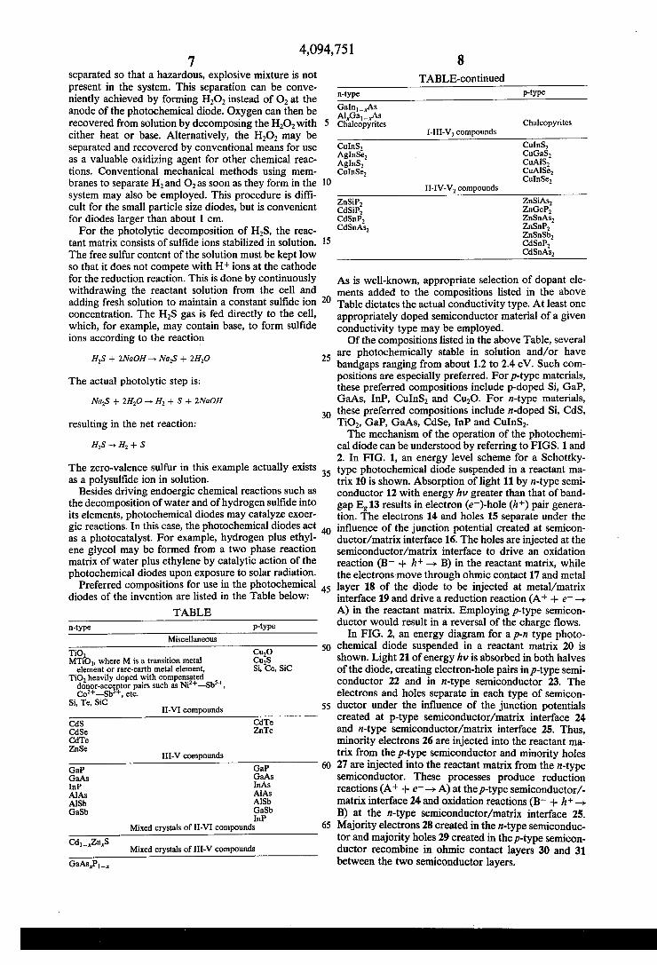
TABLE n-type P‘WPe
Miscellaneous
TiO; CuZO M1103, where M is a transition metal CuzS element or rare-earth metal element, Si, Ce, SiC
TiOz heavily doped with compensated donor-acceptor pairs such as Nth-Sb“, COZ+—Sb5+, etc.
Si, Te, SiC II-VI compounds
CdS CdTe CdSe ZnTe CdTe ZnSe
III-V compounds GaP GaP GaAs GaAs InP InAs AlAs AlAs AlSb AlSb GaSb GaSb
InP Mixed crystals of II-VI compounds
Mixed crystals of III-V compounds
20
25
35
45
50
55
60
65
8 TABLE-continued
"'WPB P'U'Pe
GalnI _xAs AlxGal _ xAs _ Chalcopyrites Chalcopyntes
As is well-known, appropriate selection of dopant ele ments added to the compositions listed in the above Table dictates the actual conductivity type. At least one appropriately doped semiconductor material of a given conductivity type may be employed. Of the compositions listed in the above Table, several
are photochemically stable in solution and/or have bandgaps ranging from about 1.2 to 2.4 eV. Such com positions are especially preferred. For p-type materials, these preferred compositions include p-doped Si, GaP, GaAs, InP, CuInSz and Cu2O. For n-type materials, these preferred compositions include n-doped Si, CdS, TiO2, GaP, GaAs, CdSe, InP and CuInS2. The mechanism of the operation of the photochemi
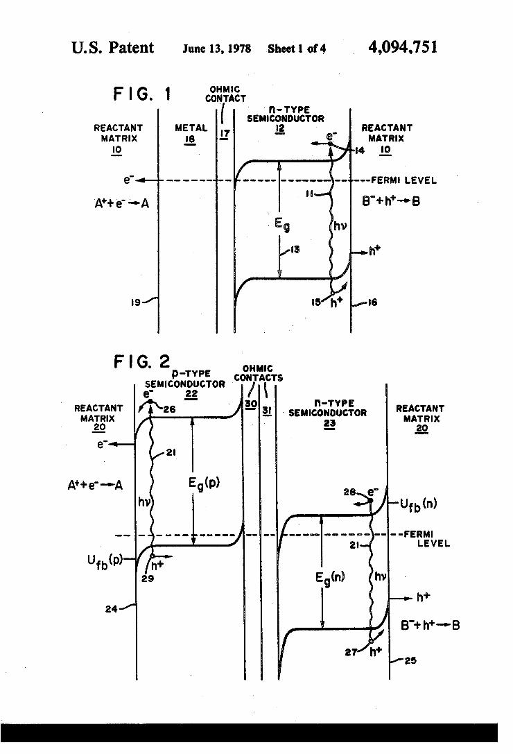
cal diode can be understood by referring to FIGS. 1 and 2. In FIG. 1, an energy level scheme for a Schottky type photochemical diode suspended in a reactant ma trix 10 is shown. Absorption of light 11 by n-type semi conductor 12 with energy hv greater than that of band gap E8 13 results in electron (e-)-hole (h+) pair genera tion. The electrons 14 and holes 15 separate under the in?uence of the junction potential created at semicon ductor/matrix interface 16. The holes are injected at the semiconductor/matrix interface to drive an oxidation reaction (B‘ + h+ —> B) in the reactant matrix, while the electrons move through ohmic contact 17 and metal layer 18 of the diode to be injected at metal/matrix interface 19 and drive a reduction reaction (A+ + e‘ -> A) in the reactant matrix. Employing p-type semicon ductor would result in a reversal of the charge flows.
In FIG. 2, an energy diagram for a p-n type photo chemical diode suspended in a reactant matrix 20 is shown. Light 21 of energy hv is absorbed in both halves of the diode, creating electron-hole pairs in p-type semi conductor 22 and in n-type semiconductor 23. The electrons and holes separate in each type of semicon ductor under the in?uence of the junction potentials created at p-type semiconductor/matrix interface 24 and n-type semiconductor/matrix interface 25. Thus, minority electrons 26 are injected into the reactant ma trix from the p-type semiconductor and minority holes 27 are injected into the reactant matrix from the n-type semiconductor. These processes produce reduction reactions (A’r + e- —> A) at the p-type semiconductor/ matrix interface 24 and oxidation reactions (B‘ + h+ -> B) at the n-type semiconductor/matrix interface 25. Majority electrons 28 created in the n-type semiconduc tor and majority holes 29 created in the p-type semicon ductor recombine in. ohmic contact layers 30 and 31 between the two semiconductor layers.
4,094,751 9
The energetics of the photochemical diodes can be understood by constructing an energy balance for the two types of diodes. For the Schottky-type diode, the following energy balance equation can be written
AG
where E3 is the bandgap of the semiconducting elec trode, VB is the band bending at the semiconductor/ma trix junction, EC is the conduction band energy, Efis the Fermi level, AG/nF is the free energy per electron for the overall chemical reaction (1.23 eV for H2O decom position), 1), and 1),. are the respective overpotentials at the anode and cathode halves of the diode, iR is the ohmic loss, and V” is the potential drop across the Helmholtz layers in the matrix; see A. J. Nozik, Vol. 29, Applied Physics Letters, pp. 150-153 (1976). The sum of the terms on the left side of Equation (1)
represent the net photon energy (as an electron-hole pair) available for doing the electrochemical work indi cated by the terms on the right side of Equation (1). The ef?ciency of the Schottky-type photochemical
diode with respect to sunlight (wavelength about 3,200 to 25,000 A) is limited by the minimum bandgap re quired to satisfy the energy balance of Equation (1). However, greatly enhanced ef?ciencies can be achieved in a pm type photochemical diode. The p- and n-type halves of the diode can-be either the same semi conductor (homotype diode) or different semiconduc tors (heterotype diode), as indicated earlier. The gross effect in the p-n photochemical diode of the
inventon is at least a partial addition, and in some cases a complete addition, of the two bandgap energies, such that higher net photon energies become available for doing reversible and irreversible electrochemical work, compared to a Schottky-type diode. This effect is a consequence of injecting minority carriers into the reac tant matrix. For a given chemical reaction, this leads to higher conversion efficiencies with respect to sunlight, since smaller bandgap semiconductors may thus be used. As is well-known, smaller bandgap semiconduc tors absorb more light and hence provide higher con version ef?ciency. The speci?c available photon energy depends upon the details of the p-n con?guration and the semiconductor properties. For the general case of a heterotype p-n photochemical diode:
E,<p) + Ego) - win) - v,.(n)1 + Am) - ABA") = (2)
ii + w) + 11.01) + iR + V”
where (p) and (n) refer to the p- and n-type semiconduc tors, respectively, AEFis the energy difference between the band edge for the majority carriers and the Fermi level, and U?, is the ?at-band potential of the semicon ductors. The latter is the semiconductor potential (with respect to the standard calomel electrode) at which the band bending V B is equal to zero; see the Applied Physics Letters reference, above. For the heterotype p-n photochemical diode, minimi
zation of the difference between the ?at-bend potentials of the p- and n-type semiconductors leads to maximiza tion of the net available photon energy. In the upper limit where this difference is zero and AEFis negligible for both semiconductors, the net available energy is
5
35
40
45
50
10 equal to the sum of the bandgap energies of the p- and n-type semiconductors. For the homotype p-n photochemical diode, the elec
tron affmities of the p- and n-type semiconductors are about equal. This leads to:
E: = $16: + 11.01) + 1;.(n) +iR + V” (3)
Thus, the net energy in this case is equal to the bandgap. For the decomposition of H20:
Hz0(l)—>11z(g) + lozts) (4)
where AH (the enthalpy change of the reaction) = +6832 kcal/mole = 2.96 eV
AG = +56.69 kcal/mole = 2.46 eV, and AG/nF = 2.46/2 = 1.23 eV.
Thus, two electron-hole pairs, each with an energy of 1.23 eV, can satisfy the free energy requirements of Equation (4). This means that at least two photons can participate in the decomposition of one water molecule. Operation of a p-n diode leads to an effective participa tion of more than two photons. Hence, photochemical diodes act as an energy upconversion device and allow the decomposition of water by using visible light; nor mally, ultraviolet light (2,430 A) is required to photo lyze water in a homogeneous system.
A. PHOTOCHEMICAL DIODE CONFIGURATIONS
1. Schottky-type Photochemical Diodes
The Schottky-type photochemical diode of the in vention comprises an appropriately doped semiconduc tor (n- or p-type), an ohmic contact to the semiconduc tor and a metallic contact to the ohmic contact, the metallic contact having high efficiency for charge (elec tron or hole) transfer to the reactant matrix. Optionally, an insulating bead may be placed on the surface of the diode between the semiconductor and metal to further improve efficiency. The bandgap of the semiconductor must be consistent with the energy balance indicated in Equation (1). The minimum bandgap is equal to the free energy change per electron, AG/nF, for the desired chemical reaction. For the decomposition of H20, AG/nF, = 1.23 eV, the bandgap range is therefore about 1.3 to 3 eV. The latter number represents the upper limit for signi?cant solar absorbance. A schematic representation of a portion of a
Schottky-type photochemical diode 32 (not to scale) suspended in a reactant matrix 33 is shown in FIG. 3. An appropriately doped semiconductor layer 34 is pro vided with an ohmic contact 35 on one face of the semi conductor layer. A metallic layer 36 is formed over the ohmic contact. The distance between the ohmic contact and the front surface 37 of the diode is made as small as possible, but consistent with achieving suf?cient optical absorption in the semiconductor layer. The semicon ductor can be made from either a single crystal, from polycrystalline material, or from amorphous material and it may be of either p- or n-type conductivity. Ab sorption of light 38 in the semiconductor layer creates electrons and holes (not shown). For n-type semicon ductors, electrons move across the ohmic contact to the metallic layer where they are injected through metal/ matrix interface 39 into the reactant matrix to produce a reduction reaction (such as H; evolution). Holes are
4,094,751 11
injected through semiconductor/matrix interface 37 into the reactant matrix to produce an oxidation reac' tion (such as O; or H202 formation). The charge flows are reversed for p-type semiconductors. In cases where the ohmic contact catalyzes hydrogen evolution, then the ohmic contact and the metallic layer are identical materials. Indium metal on CdS is an example of such a material. In practice, an assembly of the photochemical diodes is suspended in the reactant matrix.
In FIG. 4, another variation of the Schottky-type photochemical diode is shown. The device 41 operates when illuminated by light 42 from any direction. The device comprises a body with a spherical-like inner core 43 of semiconductor material, upon which are formed regular or irregular-shaped portions 44 isolated from each other. The portions 44 comprise a layer 45 in ohmic contact with the semiconductor 43 and upon which layer is deposited a metallic layer 46. In special cases, the ohmic contact and the metallic layer are iden tical materials, as discussed above. This con?guration can also be inverted such that the inner core contains a
' metal upon which are deposited isolated portions com prising a semiconducting layer deposited over an ohmic contact layer. The relative areas of the semiconductor and metal portions of the device are optimized to pro duce maximum optical absorption in the semiconductor portion and minimum resistance to H2 evolution in the metal portion.
2. p-n Type Photochemical Diodes
The p-n type photochemical diode of the invention comprises an appropriately doped p-type semiconduc tor with an ohmic contact and an appropriately doped n-type semiconductor with an ohmic contact which are intimately joined or bonded together through the re spective ohmic contacts. Optionally, an insulating bead may be placed on the surface of the diode between the p- and n-type semiconductors to further improve the ef?ciency of the diode. The p- and n-type semiconduc tors may be of the same material, except for differences in impurity doping to produce the different types of conductivity (homotype p-n photochemical diode). Al ternatively, the p- and n-type semiconductors may be made of different materials (heterotype p-n photochemi cal diode). The bandgaps of the two semiconductors must be
consistent with energy balance requirements indicated in Equation (2). The minimum bandgap requirement is that the sum of bandgaps of both semiconductors be equal to the free energy change per electron, AG/nF, for the desired chemical reaction. For the decomposi tion of H20, AG/nF = 1.23 eV. Hence, the sum of the bandgaps ranges from about 1.3 to 6.0 eV.
Portions of two types of p-n photochemical diodes (not to scale) are depicted in cross-section in FIGS. SA-B. In FIG. 5A, a side-by-side con?guration of diode 50 is shown in which light 51 is incident on the diode from one direction. In FIG. 5B, a stacked con?guration of diode 58 is shown in which light 51 is incident on the diode from opposite directions. In both cases, the diode is suspended in a reactant matrix 52. A p-type semicon ductor 53 is provided with an ohmic contact 54, and an n-type semiconductor 55 is provided with an ohmic contact 56. The two ohmic contacts are optionally con nected through a metal contact 57, which serves to act as a support for the side-by-side con?guration. The distance between the ohmic contacts 54 and 56 and the illuminated front surfaces of the semiconductors 53 and
20
25
30
40
45
50
60
65
12 55 are made as small as possible, but consistent with sufficient optical absorption in the semiconductor lay ers. The stacked con?guration depicted in FIG. 5B is related to the side-by-side con?guration depicted in FIG. 5A by topological transformations which con serve the requirements of simultaneous illumination of the p- and n-type regions of the diode and minimum distance between the surfaces of the ohmic contacts and the front illuminated surfaces of the p- and n-type semi conductors. A spherical-like diode can also be formed for a p-n
photochemical diode such that the device will operate when illuminated from any direction. Referring to FIG. 4, the inner core 43 may comprise a p- (or n-) type semiconductor while the portions 44 may comprise n (or p-) type semiconductors which are connected to the inner core through two layers of ohmic contacts (not shown), each layer making ohmic contact to each of the two types of semiconductors. A metallic layer (not shown) may be used to connect the ohmic contacts.
B. NATURE OF THE REACTANT MATRIX
The reactant matrix in which the photochemical di odes are suspended determines the resultant photo chemical reactions when the photochemical diodes are illuminated with light. The reactions can be endoergic, such as the photolytic decomposition of water into H2 plus 02 and the photolytic decomposition of hydrogen sul?de into Hz plus zero-valence sulfur, or they can be exoergic, such as the catalytic reaction of water plus ethylene to give Hz plus ethylene glycol. The reactant matrix may be a single phase of solid, liquid, or gas reactants, or a multiphase system containing two or more phases. The conductivity of the reactant matrix should be greater than about lO-4ohm-1cm-l in order to provide a low ohmic loss in the matrix and high conversion ef?ciency. Another important requirement for the reactant ma
trix is that the reactants in the matrix have effective energy levels which lie between the bandgaps of the semiconductor (Schottky-type) or semiconductors (p-n type) of the photochemical diode. This is necessary so that the photogenerated electron can be transferred from the p-semiconductor (or metal) part of the diode into the reactant matrix, and the photogenerated hole can be transferred from the n-semiconductor part of the diode into the reactant matrix, the electrons and holes being trapped at the respective reduction and oxidation levels of the constituent chemical reactants in the ma trix.
C. REACTOR SYSTEMS BASED ON PHOTOCHEMICAL DIODES
FIG. 6 is a cross-sectional view of a pipe-type reactor 61 employing photochemical diodes for the decomposi tion of water into H2 plus H202 using solar radiation in combination with solar concentrators. A transparent pipe 62 is located at the focus of a concentrating trough collector 63.. Flowing through the pipe is an electrolyte 64 containing an assembly of suspended photochemical diodes 65. Sunlight 66, collected and focused onto the pipe by the concentrator and also impinging on the pipe directly, is absorbed by the photochemical diodes. Both H2 and H202 are produced in the pipe and are separated by conventional methods after leaving the solar irradia tion section. The photochemical diodes are prevented from leaving the pipe reactor by membranes (not shown) which permit passage of liquid and gas, but not
4,094,751 13
the photochemical diodes. Fresh electrolyte is added as needed to replenish consumed electrolyte. The pipe-type reactor with trough-like solar concen
trators can be replaced by a spherical shaped reactor situated at the top of a tower situated at the focus of a collection of heliostats which are located on the ground surrounding the tower. This general type of solar en ergy system has been previously described by A. F. Hildebrandt and L. L. Vant-Hull in Vol. 18, Solar En ergy, pp. 31-41 (1976), and is used for generating heat in a working ?uid. The addition of photochemical diodes to the working ?uid thus results in generation of hydro gen in addition to heat. The two systems described above in which photo
chemical diodes are added to the working ?uid of either a pipe-type solar collector or a tower~type solar collec tor represent a hybrid cyclical solar energy conversion scheme in which solar radiation is converted into both chemical and thermal energy. Such a hybrid system has the advantage of high conversion ef?ciency and built-in energy storage. A schematic ?ow chart of such a cycli cal hybrid system is shown in FIG. 7. The hybrid sys tem, employing, for example, a working ?uid of water, is used to generate both a gaseous fuel (hydrogen) and electricity (from heated ?uids). A solar reactor 70 serves to collect and concentrate solar radiation 71 onto a working ?uid, for example, water, containing the photochemical diodes (not shown). The solar reactor can be of several designs, including the power-tower type or trough-type collector. Exit stream 73 from the solar reactor contains hot H2O and/or steam, hot Hz, and hot H202, which has been stabilized by conven tional means. This high temperature stream is passed through a thermal power generator 74, such as, for example, a steam turbine, to generate electricity. Exit stream 75 from the thermal power generator contains cooled H20, H2 and H202. H2 and 02 are recovered and separated from this stream by conventional methods in H2 separator 76 and the O2 convertor and separator 77, respectively. Exit stream 78 from the gas separators contains cold working ?uid, which is combined with fresh make-up ?uid 79 and fed back to the solar reactor 70. Any H202 that is generated is also recovered, if desired, by conventional means (not shown). An alternative procedure for operating the hybrid
photochemical-photothermal energy conversion system is to form and immediately separate H2 and O2 in the solar reactor by conventional means, such as by using selective membranes. Thus, in FIG. 7, 02 would be removed in the solar reactor and the exit stream 73 would only contain hot H2O and/or steam and hot H2, and the O2 convertor and separator 77 would not be necessary. FIG. 8 shows a cross-sectional view of a solar energy
conversion system for the generation of H; from a por tion of a large body of water, such as a lake or an ocean, using photochemical diodes. A membrane 80, permea ble to water and impermeable to the diodes, serves to con?ne an assembly of photochemical diodes 81 in a thin volume element 82 of the surface of the body of water 83. A transparent polymeric ?lm 84 covers the volume element and de?nes a space 85 in which H2 is collected. Solar radiation 86 passes through the poly meric ?lm and is absorbed in the photochemical diodes. The H2 produced is separated by conventional means (not shown) and collected and stored under the poly mer cover. The membrane maintains the photochemical diodes within the volume element and allows continu.
15
20
25
30
35
40
45
50
55
60
65
14 ous passage of fresh water into the volume and passage of any H202 produced out of the volume element to maintain an equilibrium condition.
EXAMPLES
The principle of the photochemical diode is described for three systems: n-GaP/Pt in 0.2N H2804, n-TiO2/p GaP in 0.2N H2804, and n-CdS/Pt in 1N NaOH/S=. The ?rst two systems demonstrate Schottky-type and p-n type diodes operating to decompose H2O; the third system demonstrates a Schottky-type diode decompos ing H28 The Schottky-type diodes were constructed by ?rst
evaporating metallic (ohmic) contacts on the crystals, followed by the sputtering or bonding (via silver epoxy cement) of a Pt layer. Immersion of the diode in the respective electrolyte and exposure of the semiconduc tor face either to sunlight or to simulated sunlight from a xenon lamp resulted in vigorous H2 evolution from the Pt surface. H2 evolution could also be obtained with just the ohmic contact, but the rate of evolution was not as rapid as with Pt. The p-n diode was constructed from single crystals of
n-TiO; and p-GaP bonded together through ohmic contacts with silver epoxy cement. Illumination of both sides of the sandwich structure with light resulted in formation of H2 and a combination of O2 and H202 on the p- and n-type crystals, respectively. The rate of gas formation in this system was very slow, however, due to the low conversion ef?ciency of this particular diode system.
A. PHOTOCHEMICAL DIODES IN ENDOERGIC PHOTOLYTIC REACTIONS
Example 1 A Schottky-type photochemical diode for the evolu
tion of hydrogen was constructed from n-type GaP and platinum metal. A single crystal platelet of GaP, ori ented in the (111) direction, doped with sulfur to pro— duce an n-type conductivity of 10 ohm—1cm-1 and having a thickness of 1 mm and a cross-sectional area of 0.6 cmz, was polished with 0.3 pm A1203 abrasive and then etched for 5 min at 60° C in a solution consisting of 1 part H20, 1 part H202 and 3 parts H2504. An ohmic contact was formed on the Ga face by evaporating 3000 A of a 2% Si-98% Au alloy and then heat treating the GaP crystal in H2 at 600° C for 10 minutes. A Pt ?lm with a thickness of 4000 A was deposited over the ohmic contact by DC sputtering from a Pt target. When this photochemical diode was suspended in 0.2N H2804 and the GaP face was illuminated with simulated or natural sunlight, H2 gas vigorously evolved from the Pt face. The power conversion efficiency for H2 evolu tion was about 10% conversion of incident solar radia tion.
Example 2 A Schottky-type photochemical diode was con
structed as in Example 1, except that an insulating bead of epoxy was formed around the outer edge of the diode between the Ga? and Pt faces. This resulted in a higher rate of H2 evolution.
Example 3 A Schottky-type photochemical diode was con
structed as in Example 2, except that a 1 mil Pt foil was cemented to the ohmic contact to form the diode. The
4,094,751 15
ef?ciency for H2 evolution was substantially the same as in Example 2.
Example 4 A Schottky-type photochemical diode was con
structed as in Example 2, except no Pt layer was formed over the Si-Au layer. The ohmic contact, hence, also served as the H2 evolving face. ‘The rate of H2 evolution was lower in this case.
Example 5 ' .
A 12-): type photochemical diode for the decomposi tion of water into H2 and 02 was constructed from n type TiOz and p-type GaP. A single crystal wafer of n-type rutile TiOZ, with the c-axis in the wafer plane, having a thickness of 1 mm and a cross-sectional area of 0.5 cm2,. was reduced in 1 atm of H2 at 800° C for 5 min to produce a conductivity of 0.3 ohm-lcm-l. The crys tal was etched in aqua regia at 60° C for 3 min, and a 3000 A thick layer of indium was then evaporated onto one face of the TiO; crystal to form an ohmic contact. A single crystal wafer of p-type GaP, oriented in the
(110) direction, doped with Zn to produce a p-type conductivity of 3.0 ohm- 1cm“, and having a thickness of 0.8 mm and a cross-sectional area of 0.5 cm2, was polished with 0.3 pm A1203 abrasive and then etched for 5 min at 60° C in a solution consisting of 1 part H202‘, and 1 part H20 and 3 parts H2804. An ohmic contact was then formed on one face by evaporating 3000 A of a 1% Zn-99% Au alloy, overcoating this layer with 1 pm of gold and then heat treating the GaP crystal in H2 at 600° C for 10 minutes. The n-TiO2 crystal and the p-GaP crystal were then
cemented together with silver epoxy to form a p-n type photochemical diode having a total thickness of about 2 mm and a cross-sectional area of about 0.5 cm2. An insulating head of epoxy cement was placed around the outside edge of the diode at the junction between the p-GaP and n-TiOz crystal sections. When this diode was suspended in 0.2N H2504 and
both sides of the diode illuminated with simulated sun light, H2 gas was evolved from the p-GaP face and a mixture of O2 and H202 was evolved from the n-TiOZ face. The ef?ciency for H2 evolution was about 0.3%.
Example 6 A Schottky-type photochemical diode for the decom
position of H28 into H2 and S was constructed from n-type CdS and Pt metal. A single crystal platelet of CdS having a conductivity of 2 ohm— 1cm“, a thickness of 1 mm and a cross-sectional area of 0.5 cm2, was etched in cold concentrated HCl for 1 min; an ohmic contact was then formed on one face of the platelet by evaporating 3000 A of indium and heat treating the crystal in H2 at 200° C for 5 min. A ?lm of Pt with-a thickness of 4000 A was deposited over the ohmic contact by DC sputtering from a Pt target. When this diode was suspended in a solution contain
ing lM NaOH and 1M Na2S and illuminated with natu ral sunlight or simulated sunlight, H2 gas evolved vigor ously from the Pt face. A zero-valence sulfur species was formed at the CdS face in the form of polysul?de ion. This was evidenced by a gradual change in the color of the solution from colorless to yellow as the zero-valence sulfur content increased. The Na2S was formed by passing HZS gas into NaOH solution. The ef?ciency for H2 evolution was about 7%.
15
25
30
45
50
60
65
16 Example 7
A Schottky-type photochemical diode was con structed as in Example 6, except that a 1 mil Pt foil was cemented to the ohmic indium contact to form the ‘diode structure. The ef?ciency for H2 evolution was about 7%.
Example 8
A Schottky-type photochemical diode was con structed as in Example 6, except that an insulating bead of epoxy cement was formed around the edge of the diode between the CdS and Pt sections. This resulted in a higher rate of H2 evolution. '
Example 9
A Schottky-type photochemical diode was con structed by depositing a polycrystalline thin ?lm of CdS having a thickness of 30 m, and conductivity of about 10_2ohm"cm-1 on a ?lm of conducting CdZSnO4. A Pt ?lm is also deposited on the‘ Cd5SnO4 ?lm next to the CdS ?lm.’ Illumination of the CdS ?lm with natural or simulated sunlight results in H2 evolution from the Pt ?lm and polysul?de formation at the CdS ?lm.
Example 10
An assembly of Schottky-type photochemical diodes comprising an appropriately doped semiconductor body of n-type GaP and a layer of metallic platinum intimately joined thereto is suspended in an electrolyte having a conductivity of at least about 10-4 ohm-1 cm-l. Upon exposure of the suspended assembly of photochemical diodes to solar radiation, H2 is evolved.
Example 1 1
An assembly of p-n type photochemical diodes is suspended in an electrolyte having a conductivity of about 10~4ohm—1cm—1. The diodes comprise an appro priately doped semiconductor body of n-type TiOZ provided with an ohmic contact of metallic indium and an appropriately doped semiconductor body of p-type GaP provided with an ohmic contact of a Zn-Au alloy. The ohmic' contacts are intimately joined together. Upon exposure of the suspended assembly of photo chemical diodes to solar radiation, H2 is evolved.
B. PHOTOCHEMICAL DIODES IN EXOERGIC PHOTOCATALYTIC REACTIONS
Example 12 A p-n type photochemical diode is constructed as in
Example 5. The photochemical diode is then suspended in a two phase system consisting of water and ethylene. Illumination of both sides of the diode with sunlight results in H2 evolution from the p-GaP face and ethylene glycol formation ‘on the n-TiOZ face.
Example 13
A p-nv type photochemical diode is constructed as in Example 5, except that the diode is suspended in a two phase mixture of HCl solution and ethylene. Hydrogen and ethylene dichloride are produced upon exposure of the diode to sunlight. What is claimed is: 1. A photochemical diode comprising two portions, a
?rst portion comprising at least one appropriately doped p-type' semiconductor material provided with an ohmic contact over a portion thereof and a second
4,094,751 17
portion comprising at least one appropriately doped n-type semiconductor material provided with an ohmic contact over a portion thereof and joined to said ?rst portion through both said ohmic contacts.
2. The photochemical diode of claim 1 in which the appropriately doped p-type semiconductor material consists essentially of at least one p-doped member se lected from the group consisting of Si, GaP, GaAs, InP, CuInSz and CuzO.
3. The photochemical diode of claim 1 in which the appropriately doped n-type semiconductor material consists essentially of at least one n-doped member se lected from the group consisting of Si, CdS, TiOz, GaP, GaAs, CdSe, InP and CuInSZ.
4. The photochemical diode of claim 1 additionally comprising an insulating bead on the surface of the diode between the two joined portions.
5. A process for converting optical energy into chem ical energy to drive a chemical reaction in a matrix of chemical reactants which comprises suspending an as sembly of discrete photochemical diodes in the reactant matrix and illuminating the diodes with optical energy, the diodes each comprising two portions, a ?rst portion comprising at least one appropriately doped semicon ductor material of a given conductivity type and pro vided with an ohmic contact over a portion thereof, and a second portion comprising either metal which is joined to said ?rst portion through said ohmic contact or at least one appropriately doped semiconductor ma terial of a given conductivity type opposite to that of said ?rst portion, provided with an ohmic contact over a portion thereof and joined to said ?rst portion through both said ohmic contacts.
6. The process of claim 5 in which exoergic chemical reactions in a matrix of chemical reactants are cata lyzed. -
7. The process of claim 5 in which endoergic chemi cal reactions in a matrix of chemical reactants are driven.
8. The process of claim 5 in which the optical energy is provided by solar radiation.
9. The process of claim 5 in which the chemical reac tion comprises photolytic decomposition of water into hydrogen plus at least one of oxygen and hydrogen peroxide.
10. The process of claim 5 in which the chemical reaction comprises photolytic decomposition of hydro gen sul?de into hydrogen plus zero-valence sulfur.
11. The process of claim 5 in which the ?rst portion of the diodes comprises appropriately doped p-type semiconductor material provided with an ohmic contact and the second portion of the diodes comprises appropriately doped n-type semiconductor material provided with an ohmic contact.
12. The process of claim 11 in which the relative surface areas of the p- and n-type regions are such that substantially equal rates of electron-hole pairs are gen erated in each portion.
13. The process of claim 5 in which the ?rst portion comprises appropriately doped p-type semiconductor material provided with an ohmic contact and the sec ond portion comprises metal.
14. The process of claim 5 in which the ?rst portion comprises appropriately doped n-type semiconductor material provided with an ohmic contact and the sec ond portion comprises metal.
15. The process of claim 5 in which the appropriately doped semiconductor material of a given conductivity
20
25
30
35
45
50
65
18 type consists essentially of at least one p-doped member selected from the group consisting of Si, GaP, GaAs, InP, CuInS; and Cu;().
16. The process of claim 5 in which the appropriately doped semiconductor material of a given conductivity consists essentially of at least one n-doped member se lected from the group consisting of Si, CdS, Ti02, GaP, GaAs, CdSe, InP and CuInS2.
17. The process of claim 5 in which the diodes have an average particle size less than about 0.01 micrometer and forma solution of molecular-sized diodes in the reactant matrix.
18. The process of claim 5 in which the diodes have an average particle size of about 0.01 to 0.25 micrometer and form a colloidal suspension in the reactant matrix.
19. The process of claim 5 in which the diodes have an average particle size of about 0.25 micrometer to 1 mm and are suspended in the reactant matrix by exter nal agitation.
20. The process of claim 5 in which the diodes have an average particle size greater than about 1 mm and are mechanically suspended in the reactant matrix.
21. The process of claim 5 in which the semiconduc tor material of each portion is thin enough to minimize the path length between the region where electron-hole pairs are created by action of the optical energy and the ohmic contact of the semiconductor material and thick enough to maintain suf?cient optical absorption of the optical energy.
22. The process of claim 5 in which each ohmic contact to a semiconductor material forms a surface which is parallel to the illuminated surface at that semi conductor material. -
23. A cyclical process for converting solar energy into chemical energy and thermal energy which com prises
suspending an assembly of discrete photochemical diodes in a liquid matrix, the photochemical diodes comprising two portions, a ?rst portion comprising at least one appropriately doped semiconductor material of a given conductivity type and provided with an ohmic contact over a portion thereof and a second portion comprising either metal which is joined to said ?rst portion through said ohmic contact or at least one appropriately doped semi conductor material of a conductivity type opposite to that of the ?rst portion, provided with an ohmic contact over a portion thereof and joined to said ?rst portion through both said ohmic contacts,
exposing the photochemical diodes and the liquid matrix to concentrated solar radiation,
forming gaseous fuel from the liquid matrix and unre acted matrix material at high temperature,
converting the thermal content of the high tempera ture matrix material into electricity by a thermal power generator and forming cooled matrix mate rial,
recovering the gaseous fuel from the cooled matrix material,
adding fresh liquid matrix to the cooled matrix mate rial, and
recycling the matrix material for reexposure to the concentrated solar radiation.
24. The process of claim 23 in which the matrix com prises water and the gaseous fuel comprises hydrogen.
25. A process for generating hydrogen from a portion of a body of water using solar radiation comprising
4,094,751 19
suspending an assembly of discrete photochemical diodes in the water, the photochemical diodes comprising two portions, a ?rst portion comprising at least one appropriately doped semiconductor material of a given conductivity type and provided with an ohmic contact over a portion thereof and a second portion comprising either metal which is joined to said ?rst portion through said ohmic contact or at least one appropriately doped semi conductor material of a conductivity type opposite to that of said ?rst portion, provided with an ohmic contact over a portion thereof and joined to said ?rst portion through both said ohmic contacts,
con?ning the diodes to a ?xed volume element by membranes permeable to the water and imperme able to the diodes, and
collecting evolved hydrogen in a space above the water formed by a transparent polymer ?lm.
26. In combination: (a) a matrix of chemical reactants; and (b) an assembly of discrete photochemical diodes
suspended in the reactant matrix, the photochemi cal diodes comprising two portions, a ?rst portion comprising at least one appropriately doped semi conductor material of a given conductivity type and provided with an ohmic contact over a portion thereof and a second portion comprising either metal which is joined to said ?rst portion through said ohmic contact or at least one appropriately doped semiconductor material of a conductivity type opposite to that of said ?rst portion, provided with an ohmic contact over a portion thereof and joined to said ?rst portion through both said ohmic contacts.
27. The combination of claim 26 in which the matrix of chemical reactants contains substances for exoergic chemical reactions catalyzed by the assembly of photo chemical diodes.
28. The combination of claim 26 in which the matrix of chemical reactants contains substances for endoergic chemical reactions catalyzed by the assembly of photo chemical diodes.
29. The combination of claim 26 further comprising
15
20
25
30
40
20 30. The combination of claim 26 in which the matrix
of chemical reactants includes a solution comprising water.
31. The combination of claim 26 in which the matrix of chemical reactants includes a solution comprising hydrogen sul?de.
32. The combination of claim 26 in which the diodes have an average particle size less than about 0.01 mi crometer and form a solution of molecular-sized diode in the reactant matrix.
33. The combination of claim 26 in which the diodes have an average particle size of about 0.01 to 0.25 mi crometer and form a colloidal suspension in the reactant matrix.
34. The combination of claim 26 in which the diodes have an average particle size of about 0.25 micrometer to 1 mm and are suspended in the reactant matrix by external agitation.
35. The combination of claim 26 in which the diodes have an average particle size greater than about 1 mm and are mechanically suspended in the reactant matrix.
36. The combination of claim 26 in which the ?rst portion of the diodes comprises appropriately doped p-type semiconductor material provided with an ohmic contact and the second portion of the diodes comprises appropriately doped n-type semiconductor material provided with an ohmic contact.
37. The combination of claim 26 in which the first portion of the diodes comprises appropriately doped p-type semiconductor material provided with an ohmic contact and the second portion comprises metal.
38. The combination of claim 26 in which the ?rst portion of the diodes comprises appropriately doped n-type semiconductor material provided with an ohmic contact and the second portion comprises metal.
39. The combination of claim 26 in which the appro priately doped semiconductor material of a given con ductivity type consists essentially of at least one p doped member selected from the group consisting of Si, GaP, GaAs, InP, CuInS; and CuZO.
40. The combination of claim 26 in which the appro priately doped semiconductor material of a given con ductivity type consists essentially of at least one n doped member selected from the group consisting of Si,
means for impinging solar radiation on the assembly of 45 CdS, TiOZ, GaP, GaAs, CdSe, InP and CuInS2. # * photochemical diodes.
50
55
65
i i t
UNITED STATES PATENT OFFICE Page 1 of 2
CERTIFICATE OF CORRECTION
Patent No. 14,09L+,751 , Dated June 15, 1978
Inventor(s) Arthur 'I- NOZik
It is certified that error appears in the above-identified patent and that said Letters Patent are hereby corrected as shown below:
. 0
Col. 3, line 53, "A" should read --A--. ' 0
Col. 5, line 51, "A" should read --A--.
Col. 7, line 53, "Ce" should read —-Ge—-. 0
Col. 9, line 25, "A" should read --A--. 0
Col. 10, line 29, "A" should read —-A--. 0
Col. 14, line 47, "A" should read —-A--. 0
Col. 14, line 49 , "A" should-read —-Ar—-. 0
Col. 15, line 20, "A" should read --A-—. 0
Col. 15, line 29, "A" should read --A--.
UNITED STATES PATENT OFFICE Page 2 Of 2
‘ CERTIFICATE OF CORRECTION
Patent No. 'lHO9Lh75l Dated June 15, 1978
Inventor ( 5) Arthur J ' NoZj-k
It is certified that error appears in the above-identified patent and that said Letters Patent are hereby corrected as shown below:
Col. 15, line 55, "A" should read “13".
C01. 15', line 57, "A" should read +13".
Col. 18, line 55, "at" should read --of--.
Col. 20, line 9, "diode" should read --diodes--.
Signed and Scaled this Fourteenth Day of August 1979
[SEAL] Attest:
LUTRELLE F. PARKER Attestiug O?Fcer Acting Commissioner of Patents and Trademarks


![United States Patent [191 [11] Patent Number: 5,389,382 [45] Date … · 2017. 4. 6. · United States Patent [191 List et a1. USOO5389382A [11] Patent Number: [45] Date of Patent:](https://static.documents.pub/doc/80x56/60bd3e45b423d52f4d291c3d/united-states-patent-191-11-patent-number-5389382-45-date-2017-4-6.jpg)
![United States Patent [191 [11] Patent Number: …United States Patent [191 [11] Patent Number: 4,621,706 Boyesen [45] Date of Patent: Nov. 11, 1986 [54] MOTORCYCLE DRIVE WHEEL 3,917,313](https://static.documents.pub/doc/80x56/5ec7d8ba721a6d486206c27c/united-states-patent-191-11-patent-number-united-states-patent-191-11-patent.jpg)
![United States Patent pi] - NASA · 2013-04-10 · United States Patent US005429997A [191 pi] Patent Number: 5,429,997 - 1 I I ... Material Science and Technology Division Eng. A155,](https://static.documents.pub/doc/80x56/5edb55c2ad6a402d666580c7/united-states-patent-pi-nasa-2013-04-10-united-states-patent-us005429997a-191.jpg)
![United States Patent Patent Number: 4,726,069 Date of · United States Patent [191 Stevenson [11] ... modulation and signal processing for single sideband communications systems which](https://static.documents.pub/doc/80x56/5af92c7c7f8b9a32348c0d1b/united-states-patent-patent-number-4726069-date-of-states-patent-191-stevenson.jpg)


![United States Patent [191 4,667,290 Goss et al. May …United States Patent [191 Goss et al. [54] COMPILERS USING A UNIVERSAL INTERMEDIATE LANGUAGE [75] Inventors: Clinton Goss, New](https://static.documents.pub/doc/80x56/5f1038da7e708231d4480b4b/united-states-patent-191-4667290-goss-et-al-may-united-states-patent-191-goss.jpg)

![United States Patent [191 [11] 4,146,499](https://static.documents.pub/doc/80x56/613d73c9736caf36b75d7fd1/united-states-patent-191-11-4146499.jpg)

![United States Patent 5,768,242 - NASA · United States Patent [191 [ill Patent Number: 5,768,242 Juday [45] Date of Patent: Jun. 16, 1998 41 APPARATUS AND METHOD FOR FOCUSING DIMENSIONAL](https://static.documents.pub/doc/80x56/5f0b5b997e708231d4301efd/united-states-patent-5768242-nasa-united-states-patent-191-ill-patent-number.jpg)


