(12) United States Patent Hu et al. (54) TERAHERTZ LASERS AND AMPLIFIERS BASED ON RESONANT OPTICAL PHONON SCATTERING TO ACHIEVE POPULATION INVERSION (75) Inventors: Qing Hu, Wellesley, MA (US); Benjamin S. Williams, Cambridge, MA (US) (73) Assignee: Massachusetts Institute of Technology, Cambridge, MA (US) Subject to any disclaimer, the term of this patent is extended or adjusted under 35 U.S.C. 154(b) by 150 days. ( * ) Notice: (21) Appl. No.: 10/661,831 (22) Filed: Sep. 12, 2003 (65) Prior Publication Data US 200510058168 A1 Mar. 17, 2005 (51) Int. C1. (52) U.S. C1. ...................................... 372/4; 372145.012 (58) Field of Classification Search ........... 372145.012, 37214 HOlS 5/00 (2006.01) See application file for complete search history. (56) References Cited U.S. PATENT DOCUMENTS 5,457,709 A 5,509,025 A 5,745,516 A 5,936,989 A 6,144,679 A 6,154,475 A 6,188,477 B1 6,370,219 B1 6,472,683 B1 6,563,622 B1 6,829,269 B1 * 10/1995 4/1996 4/1998 8/1999 11/2000 11/2000 2/200 1 4/2002 10/2002 5/2003 12/2004 Capasso et al. Capasso et al. Capasso et al. Capasso et al. Herman et al. Soref et al. Pu et al. Peale Li Mueller et al. Goodhue et al. ........ 46 372/43.01 (io) Patent No.: (45) Date of Patent: US 7,158,545 B2 Jan. 2,2007 2003/0219052 A1 * 11/2003 Goodhue et al. ............. 372/45 OTHER PUBLICATIONS Williams et al. “3.4 THz quantum cascade laser operating above liquid nitrogen temperature” Elec. Letter., vol. 39, No. 12 (Jun. 12, 2003).* Kazarinov and Suris, “Possibility of the amplification of electro- magnetic waves in a semiconductor and superlattice,” Sov. Phys. Semicond. 5, 707 (1971). Faist, et al., “Quantum cascade laser,” Science 264, 477 (1994). Beck, et al., “Continuous Wave Operations of a Mid-infrared Semiconductor Laser at Room Temperature,” Science 295, 301 Helm, et al., “Intersubband Emission from Semiconductor Superlat- tices Excited by Sequential Resonant Tunneling,” Phys. Rev. Lett. 63, 74 (1989). (2002). (Continued) Primary Examiner-Minsun Oh Harvey Assistant Examiner-Tod T. Van Roy (74) Attorney, Agent, or Firm-Thomas J. Engellenner; Reza Mollaaghababa; Nutter McClennen & Fish LLP (57) ABSTRACT The present invention provides quantum cascade lasers and amplifier that operate in a frequency range of about 1 Terahertz to about 10 Terahertz. In one aspect, a quantum cascade laser of the invention includes a semiconductor heterostructure that provides a plurality of lasing modules connected in series. Each lasing module includes a plurality of quantum well structure that collectively generate at least an upper lasing state, a lower lasing state, and a relaxation state such that the upper and the lower lasing states are separated by an energy corresponding to an optical fre- quency in a range of about 1 to about 10 Terahertz. The lower lasing state is selectively depopulated via resonant LO-phonon scattering of electrons into the relaxation state. 28 Claims, 10 Drawing Sheets . ..... https://ntrs.nasa.gov/search.jsp?R=20080009470 2018-05-26T19:12:16+00:00Z
Transcript
(12) United States Patent Hu et al.
(54) TERAHERTZ LASERS AND AMPLIFIERS BASED ON RESONANT OPTICAL PHONON SCATTERING TO ACHIEVE POPULATION INVERSION
(75) Inventors: Qing Hu, Wellesley, MA (US); Benjamin S. Williams, Cambridge, MA (US)
(73) Assignee: Massachusetts Institute of Technology, Cambridge, MA (US)
Subject to any disclaimer, the term of this patent is extended or adjusted under 35 U.S.C. 154(b) by 150 days.
( * ) Notice:
(21) Appl. No.: 10/661,831
(22) Filed: Sep. 12, 2003
(65) Prior Publication Data
US 200510058168 A1 Mar. 17, 2005
(51) Int. C1.
(52) U.S. C1. ...................................... 372/4; 372145.012 (58) Field of Classification Search ........... 372145.012,
37214
HOlS 5/00 (2006.01)
See application file for complete search history.
(56) References Cited
U.S. PATENT DOCUMENTS
5,457,709 A 5,509,025 A 5,745,516 A 5,936,989 A 6,144,679 A 6,154,475 A 6,188,477 B1 6,370,219 B1 6,472,683 B1 6,563,622 B1 6,829,269 B1 *
10/1995 4/1996 4/1998 8/1999
11/2000 11/2000 2/200 1 4/2002
10/2002 5/2003
12/2004
Capasso et al. Capasso et al. Capasso et al. Capasso et al. Herman et al. Soref et al. Pu et al. Peale Li Mueller et al. Goodhue et al. ........
46
372/43.01
(io) Patent No.: (45) Date of Patent:
US 7,158,545 B2 Jan. 2,2007
2003/0219052 A1 * 11/2003 Goodhue et al. ............. 372/45
OTHER PUBLICATIONS
Williams et al. “3.4 THz quantum cascade laser operating above liquid nitrogen temperature” Elec. Letter., vol. 39, No. 12 (Jun. 12, 2003).* Kazarinov and Suris, “Possibility of the amplification of electro- magnetic waves in a semiconductor and superlattice,” Sov. Phys. Semicond. 5, 707 (1971). Faist, et al., “Quantum cascade laser,” Science 264, 477 (1994). Beck, et al., “Continuous Wave Operations of a Mid-infrared Semiconductor Laser at Room Temperature,” Science 295, 301
Helm, et al., “Intersubband Emission from Semiconductor Superlat- tices Excited by Sequential Resonant Tunneling,” Phys. Rev. Lett. 63, 74 (1989).
(2002).
(Continued)
Primary Examiner-Minsun Oh Harvey Assistant Examiner-Tod T. Van Roy (74) Attorney, Agent, or Firm-Thomas J. Engellenner; Reza Mollaaghababa; Nutter McClennen & Fish LLP
(57) ABSTRACT
The present invention provides quantum cascade lasers and amplifier that operate in a frequency range of about 1 Terahertz to about 10 Terahertz. In one aspect, a quantum cascade laser of the invention includes a semiconductor heterostructure that provides a plurality of lasing modules connected in series. Each lasing module includes a plurality of quantum well structure that collectively generate at least an upper lasing state, a lower lasing state, and a relaxation state such that the upper and the lower lasing states are separated by an energy corresponding to an optical fre- quency in a range of about 1 to about 10 Terahertz. The lower lasing state is selectively depopulated via resonant LO-phonon scattering of electrons into the relaxation state.
Kohler, et al., “Terehertz semiconductor-heterostmcture laser,” Nature, 417, 156 (2002). Tredicucci et al. “High performance interminiband quantum cas- cade lasers with graded superlattice,” Appl. Phys. Letter. 73, 2101 (1998). Rochat, et al., “Low-threshold terahertz quantum-cascade lasers,” Appl. Phys. Lett. 81, 1381 (2002). Williams, et al., “3.4-THz quantum cascade laser based on Longitudunal-optical-phonon scattering for depopulation,” Appl. Phys., Lett. 82, 1015 (2003). Also published in Virtual Journal of Nanoscale Science & Technology, 7(8) (2003). Unterrainer, et al., “Quantum cascade lasers with double metal- semiconductor waveguide resonators,” Appl. Phys. Lett. 80, 3060
Lee, et al., “Au-In bonding below the eutectic temperature,” IEEE Trans. Comp, Hybrids, Manuf. Technol. 16, 311 (1993). Wang, et al., “Die bonding with AdIn isothermal solidification technique,” J. Electron. Mat. 29, 443 (2000). Wang, et al., “Stable and shallow Pdln ohmic contancts to n-GaAs,” Appl. Phys. Lett. 56, 2129 (1990).
(2002).
Troccoli, et al., “Mid-infrared (n = 7.4 um) quantum cascade laser amplifier for high power single-mode emission and improved beam quality,” Appl. Phys. Lett. 80, 4103 (2002). Mueller, et al., “2.5 THz Laser Local Oscillator for the EOS Chem 1 Satellite,” Proceedings of the Ninth International Space Terahertz Technology Symposium, pp. 563-572, Pasadena, CA, Mar. 17-19 (1998). Williams, et al., “Narrow-linewidth terahertz intersubband emission from three-level systems,” American Institute of Physics (1999). Williams and Hu, “Optimized energy separation for phonon scat- tering in three-level terahertz intersubband lasers,” American Insti- tute of Physics (2001). Xu and Hu, “Electrically pumped tunable terahertz emitter based on intersubband transition,” American Institute of Physics (1997). Faist, et al., “Bound-to-Continuum and Two-Phonon Resonance Quantum-Cascade Lasers for High Duty Cycle, High-Temperature Operation,” IEEE (2002).
* cited by examiner
FIG. 1
I
12 24
FIG. 2
GaAs UNDOPED 81.9 A (29 MU
A10.15Gao. 25As UNDOPED 25.4 A ( 9 MLI
Ga As UNDOPED 67.8 A (24 ML)
A10. ~ s G ~ o . 25As UNDOPED 39.6 A (14 ML)
GaAs 1.gx&m3 155.4 A (55 ML)
A $ , 25As UNDOPED 25.4 A ( 9 ML)
GaAs UNDOPED 98.9 A (35 ML)
15Ga0. 25As UNDOPED 56.5 A (20 ML)
nt GaAs SUBSTRATE
14 Au
“-ntt\
A
REPEAT 17 5
TIMES
3 3 h)
h) 0 0 4
CI
0 ,, CI 0
U.S. Patent Jan. 2,2007 Sheet 2 of 10
FIG. 3A
US 7,158,545 B2
32
294 . gGaO. gAs
(20 nm) (1000 nm)
Au (120 nml
(500 nml
r
nt GaAs RECEPTOR SUBSTRATE
\ 34
I I 1
FIG. 38 26
FIG. 3C
I n+ GaAs RECEPTOR SUBSTRATE I
U.S. Patent Jan. 2,2007 Sheet 3 of 10
42 1
F I G . 30 Au 40
AU
US 7,158,545 B2
Au
I n+ GaAs RECEPTOR SUBSTRATE
FIG. 3E
TilAu {201200 nm)
n+ GaAs RECEPTOR SUBSTRATE
U.S. P:
MODE INTENSITY
( a . u . 1
MODE INTENSITY
( a . u . 1
Ltent Jan. 2,2007 Sheet 4 of 10
F I G . 4A
US 7,158,545 B2
- Au ACTIVE 11
REGION SEMI INSULATING GaAs SUBSTRATE
FIG. 48
r - - - - - - - i I l e
- Au
I
'I
ACTIVE REGION
Au
20
. . . . . . - .
30 40
13
12
Re { E )
11
10
13
12
Re {&I
11
10
DISTANCE (nm)
U.S. Patent Jan. 2,2007 Sheet 5 of 10 US 7,158,545 B2
FIG. 5
46
Egq=13.2 meV : m
U.S. Patent Jan. 2,2007 Sheet 6 of 10
58 COOLANT
MIRROR-
60 1
56 DEVICE
FIG. 6
62 DETECTOR
US 7,158,545 B2
BSJ : : I I I I I I -
FTIR [ 1 1 I SPECTROMETER
I LOCK-IN AMPLIFIER
TRANSLATING / MIRROR MIRROR POSITION
r PC
U.S. Patent Jan. 2,2007 Sheet 7 of 10 US 7,158,545 B2
FIG. 7 WAVELENGTH h m )
82 80 78 76
5- 70 K
INTENSITY (a.u.1 - -
0 3.65 3 . 7 3.75 3.8 3.85 3.9 3.95
FREQUENCY (THz)
FIG. 8
68 nt GaAs
U.S. Patent Jan. 2,2007 Sheet 8 of 10
FIG. 9
US 7,158,545 B2
CURRENT DENSITY (A /cm2)
0 200 400 600 800 io00 12 00
10
BIAS IVI
5
0
CURRENT ( A I r( 76
I I
0 50 1
\
15
10
PEAK OPTICAL
POWER (mW)
5
TEMPERATURE (KI
U.S. Patent Jan. 2,2007 Sheet 9 of 10
0-
FIG. 10
- 5 .30 A
5.18 A
5.07 A
US 7,158,545 B2
-
-
10
8
6 INTENSITY
(a.u.1 4
2
4 . 9 4 A
4.80 A
4.72 A
- -
WAVELENGTH (um) 120 115 110 105 100 95 90 85 I
3.38 THz 14 .O meV 88.6 urn
T=78 K
\
0
I I
2 .6 2.8 3 3.2 3 .4 3 .6 FREQUENCY (THz)
/ 78
INTENSITY (a.u.1
3: 3 3: 4 3:5 3.6 FREQUENCY ( THz)
U.S. Patent Jan. 2,2007 Sheet 10 of 10 US 7,158,545 B2
FIG. 11 ao
93,
US 7,158,545 B2 1 2
TERAHERTZ LASERS AND AMPLIFIERS BASED ON RESONANT OPTICAL PHONON SCATTERING TO ACHIEVE POPULATION
INVERSION
difficulties associated with mode confinement, at these fre- quencies contribute to challenges in developing such lasers.
Hence, there is a need for coherent terahertz radiation sources, particularly, coherent sources that generate radia-
5 tion in a frequency range of about 1 to about 10 THz. STATEMENT REGARDING FEDERALLY There is also a need for efficient methods for mode
confinement in such terahertz lasers. SPONSORED RESEARCH
This invention was made with government support under Contract No. PO#P927326 awarded by AFOSR, Contract No. NAG5-9080 awarded by NASA, and Contract No. ECS-0217782 awarded by NSF. The government has certain rights in the invention.
BACKGROUND OF THE INVENTION
The present invention pertains generally to quantum cas- cade lasers (QCL), and more particularly, it relates to
SUMMARY OF THE INVENTION 10
In one aspect, the present invention provides terahertz quantum cascade lasers that operate in a frequency range of about 1 to about 10 Terahertz. A quantum cascade laser of the invention can include an active region generally formed
15 as a semiconductor heterostructure that provides a plurality of lasing modules connected in series. Each lasing module includes at least an upper lasing state, a lower lasing state and a relaxation state. The upper and the lower lasing states
quantum cascade lasers that operate in the terahertz region are separated in energy by a value corresponding to an of the electromagnetic spectrum. 20 optical frequency in a range of about 1 to about 10 Terahertz.
The terahertz region (e.g., -1-10 THz, corresponding to Hence, optical radiative transitions between the upper lasing a wavelength 2~30-300 pm or a photon energy ho-4-40 state and the lower lasing state generate radiation having a meV) of the electromagnetic spectrum falls between micro- frequency in a range of about 1 to about 10 Terahertz. waveimillimeter and near-infraredioptical frequency ranges. Applicants have discovered that a highly selective and Numerous coherent radiation sources have been developed 25 very fast depopulation of the lower lasing state can be in the microwaveimillimeter and near-infraredioptical fre- achieved by employing resonant LO-phonon scattering of quency ranges. However, despite potential applications of electrons populating the lower lasing state into the relaxation terahertz radiation in a variety of different fields (e.g., state. For example, the rate of depopulation scattering can be spectroscopy in chemistry and biology, plasma diagnostics, higher than lo1’ s-l (a lifetime of the lower lasing state remote atmospheric sensing and monitoring, and detection 30 being less than 1 psec), and further it can be largely of bio- and chemical agents and explosives for security and insensitive to operating temperature. This feature advanta- military applications), coherent radiation sources operating geously facilitates generation of a population inversion in the terahertz region remain scarce. The difficulties in between the upper and the lower lasing states. More par- developing such radiation sources can be appreciated by ticularly, the energy separation of the lower lasing state and considering that semiconductor devices, such as, G u m 35 the relaxation state is designed to allow resonant LO-phonon oscillators, or Schottky-diode frequency multipliers, that scattering of electrons from the lower lasing state into the utilize classical real-space charge transport for generating relaxation state. In other words, this energy separation is radiation exhibit power levels that decrease as the fourth approximately equal to the energy of at least one LO-phonon power of radiation frequency mode of the heterostructure.
As is known in the art, the rate of radiative transitions between the lasing states and the non-radiative transitions between the lasing states and the relaxation state are deter- mined not only by energy separation between these states, but also by the shapes of the wavefunctions associated with
45 these states. In a terahertz laser of the invention, the wave- as the radiation frequency (f) increases above 1 THz. Fur- function of the lower lasing state of each lasing module has ther, the radiation frequencies obtained from photonic or a substantial coupling to that of the relaxation state while the quantum electronic devices, such as laser diodes, are limited corresponding coupling between the upper lasing state and by the semiconductor energy bandgap of such devices, the relaxation state is substantially diminished. This can be which is typically higher than 10 THz even for narrow gap 50 accomplished, for example, by placing another state (e.g., lead-salt materials. Thus, the frequency range below 10 THz level 3 in FIG. 5) at resonance with the lower lasing state. is not accessible by employing conventional semiconductor This other state, which can be primarily located in the same laser diodes. well as the relaxation state, couples strongly with the relax-
Some unipolar quantum well semiconductor lasers oper- ation state. When this other state (level 3) and the lower ating in the mid-infrared portion of the electromagnetic 55 lasing state (e.g., level 4 in FIG. 5) are brought into spectrum are known. For example, electrically pumped resonance through a bias voltage, the lower lasing state unipolar intersubband transition lasers, commonly known becomes strongly coupled to the relaxation state as well. also as quantum cascade lasers, operating at a wavelength of However, the upper lasing state (e.g., level 5 in FIG. 5) is far 4 microns were developed at Bell Laboratories in 1994. from resonance and only weakly coupled to the relaxation Since then, major improvements in power levels, operating 60 state. As a result, despite a small energy separation between temperatures, and frequency characteristics have been made the upper and the lower lasing states relative to their energy for mid-infrared QCLs. separation from the relaxation state, the lower lasing state
In contrast to such developments of QCL’s in the mid- exhibits non-radiative transition rate into the relaxation state infrared range, the development of terahertz quantum cas- that is considerably faster (e.g., by a factor of -10) than the cade lasers in a frequency range below 10 THz has been 65 corresponding transition rate of the upper lasing state. For considerably more challenging. In particular, small separa- example, a ratio of the non-radiative transition rate of the tion of lasing energy levels (about 10 mev), coupled with lower lasing state into the relaxation state relative to a
40
($1
US 7,158,545 B2 3 4
corresponding rate of the upper lasing state can be in a range FIG. 2 is a cross-sectional view of the laser of FIG. 1 of about 5 to about 10. These factors enhance the non- illustrating a heterostructure forming the laser's active radiative lifetime of the upper lasing state relative to that of region, the lower lasing state, thereby facilitating generation of a FIGS. 3A-3E schematicah' illustrate ~ r i o u s steps in an population inversion between these two states. For example, 5 exemplary fdxkation method for generating a double-sided the lifetime of the upper lasing state can be approximately 10 metal waveguide for use in a terahertz laser according to one times longer than that of the lower lasing state. In addition, embodiment Of the invention, the wavefunctions of the upper and lower lasing states are designed such that their coupling is
4A depicts graphs Of mode profile and the constant in various layers Of a quantum strong to part Of
i o cascade laser according to one embodiment of the invention allow fast radiative transitions between the upper and the at a wavelength of 100 microns and utilizing a waveguide lower lasing states, thereby enhancing lasing efficiency. formed of a metal layer and a heavily doped semiconductor
In one aspect, a quantum cascade laser of the invention layer for mode confinement, includes electrical contacts that can apply a bias voltage FIG. 4B depicts graphs of calculated mode profile and the across the heterostructure forming the active region of the 15 real part of dielectric constant in various layers of a quantum laser. The bias voltage causes a shift in the energy levels of cascade laser according to another embodiment of the inven- various states of the lasing modules such that a relaxation tion at a wavelength of 100 microns and utilizing a double- state of each module is in substantial resonance with an sided metal waveguide for mode confinement, upper lasing state of an adjacent module to allow resonant FIG. 5 illustrates an exemplary calculated conduction tunneling of electrons from the relaxation state into the 20 band profile of two lasing modules of a quantum cascade adjacent upper lasing state. laser fabricated in accordance with the teachings of the
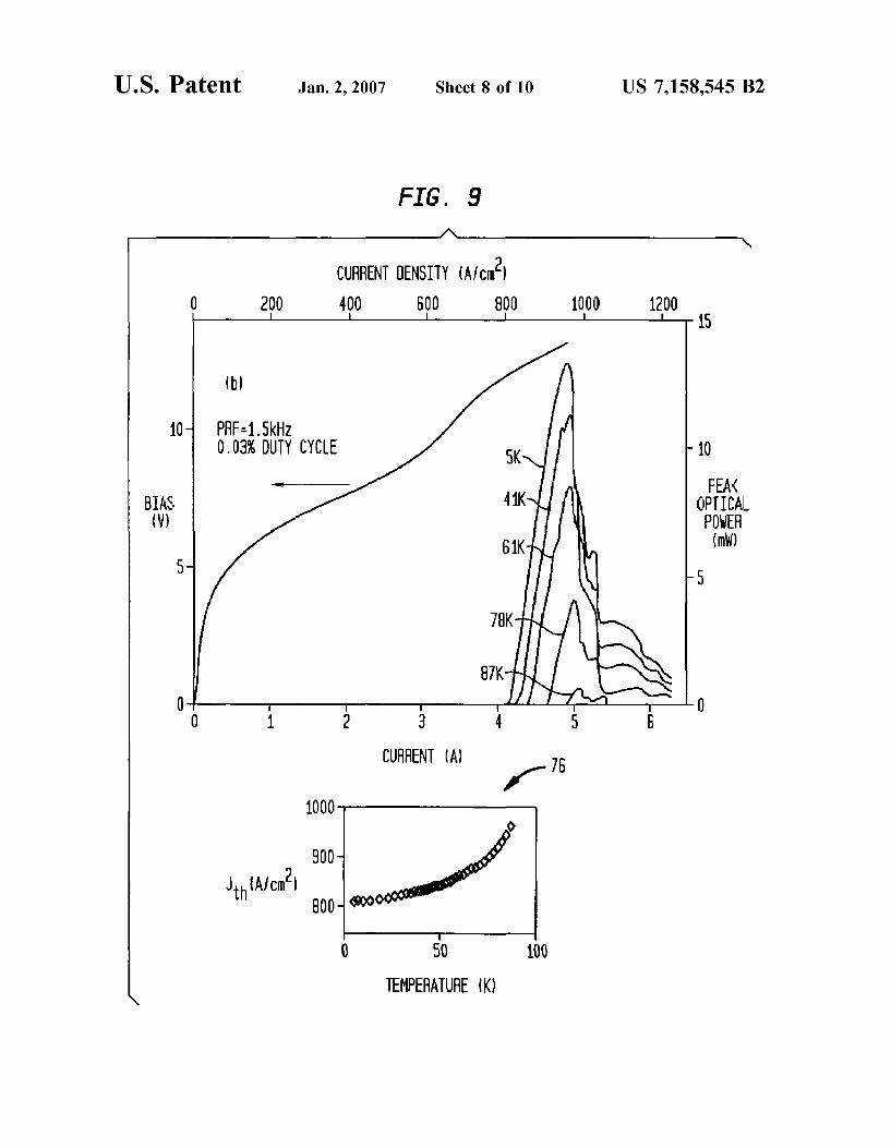
An active region of a quantum cascade laser of the invention, invention as described above can be formed, for example, as FIG. 6 is a schematic diagram of an experimental mea- a cascaded series of alternating layers of GaAs and A1,Ga- surement system for testing proto-type quantum cascade As sandwiched between an upper contact layer and a lower 25 lasers formed in accordance with the teachings of the contact layer, wherein the aluminum concentration (x) can invention, range from about 15% to about 30%, and the gallium FIG. 7 illustrates a plurality of measured emission spectra concentration (y) can range from about 65% to about 80%. of an exemplary quantum cascade laser formed in accor- Those having ordinary skill in the art will appreciate it that dance with the teachings of the invention, other concentration ranges may also be suitable for the 30 FIG. 8 is a perspective view of a quantum cascade laser practice of the invention. The contact layers can be, for according to one embodiment of the invention, which uti- example, heavily doped (e.g., with Si dopants that provide lizes surface plasmon for mode confinement, n-typE doping) GaAs layers (e.g., a doping level of about FIG. 9 presents graphs illustrating bias voltage versus 3x10 cm-'). The heterostructure and the contact layers can injected current, as well as optical power as a function of be formed on a semi-insulating substrate, e.g., a semi- 35 current, in a proto-type laser formed in accordance with the insulating GaAs layer. embodiment of FIG. 8,
a related aspect, a quantum cascade laser of the FIG. 10 illustrates a plurality of measured emission spec- invention can include a coupled to the active tra obtained from a proto-type laser formed in accordance region for confining selected lasing modes. Such a with the embodiment Of
and a heavily doped semiconductor layer, for example, a amplifier fabricated in accordance with the teachings of the heavily doped GaAs layer, that provides mode confinement invention. via surface plasmons. More preferably, the waveguide is formed of two metallic layers, for example, two gold layers,
With reference to FIGS. 1 and 2, an exemplary quantum A terahertz quantum cascade laser Of the invention has cascade laser 10 according to one exemplary embodiment of
been demonstrated to operate at temperatures up to about the invention includes an active lasing region 12 formed as
50 GaAs substrate) 14. The active region 12, which can have a K). Generally, the invention provides the opportunity for
higher temperature (for example, at room temperature) (in this exemplary embodiment, the active region has a In another aspect, the invention provides an amplifier thickness of about 10 microns), includes a plurality of
capable of operating in a range of about 1 to about 10 THz cascaded nominally identical repeat lasing modules 16, that includes an amplification region formed as a hetero- 55 which are coupled in series, The number of the lasing Structure that Provides an upper and a hwer amplification modules can range, for example, from about 100 to about states and a relaxation state. The lower amplification state 200, this exemplary embodiment, the number of lasing exhibits a non-radiative coupling to the relaxation state via modules is selected to be 175, resonant LO-phonon scattering. The amplifier includes an Each lasing module can be formed as a G ~ A ~ / input port for optically coupling incoming radiation to the 60 Al,,,Ga,,,As heterostructure. For example, as shown in amplification region to generate an amplified signal that can FIG, 1, in this embodiment, each lasing module, which has be extracted from the amplifier via an output port. an approximate thickness of 600 angstroms, is formed as a
stack of alternating Al,,,Ga,,,As and GaAs layers having the illustrated thicknesses. The heterostructure of each las-
65 ing module provides four quantum wells that collectively generate lasing and relaxation states, as described in more detail below. More particularly, each GaAs layer sand-
8, and waveguide can be formed, for example, as a metallic layer 40 l1 is a schematic perspective view Of a terahertz
DETAILED DESCRIPTION
between which the active region is disposed. 45
137 (e.g.> at temperatures in a range Of about 5K to 137 a heterostructure on a G A S substrate (for example, an n+
fabricating quantum cascade lasers that can 'perate at even thickness in a range of about 3 microns to about 10 microns
BRIEF DESCRIPTION OF THE DRAWINGS
FIG. 1 is a perspective schematic view of a quantum laser according to the teachings of the invention,
US 7,158,545 B2 5 6
wiched between two Al,,,Ga,,,As barrier layers functions nm) and a layer 30 of gold (e.g., a thickness of about 1000 as a two-dimensional quantum well. nm). Further, a receptor wafer 32 is prepared by depositing
The term “quantum well” is known in the art. To the successive layers of palladium (Pd), germanium (Ge), pal- extent that a definition may be needed, a “quantum well,” as ladium (Pd), indium (In), and gold (Au) on a doped n+ GaAs used herein, refers to a generally planar semiconductor 5 substrate 34. The PdGeiPd multi-layer advantageously region, having a selected composition, that is sandwiched improves electrical contact to the receptor layer while the between semiconductor regions (typically referred to as topmost gold layer minimizes oxidation of the indium layer. barrier layers) having a different composition, commonly With reference to FIG. 3B, the two wafers 26 and 32 are selected to exhibit a larger bandgap energy than that of the bonded together and the GaAs layer 29 is removed. For composition ofthe quantum well layer. The spacing between i o example, in this exemplary embodiment, wafer pieces hav- the barrier layers, and consequently the thickness of the ing a cross-sectional area of about 1 cm-’ were cleaved and quantum well layer, are selected such that charge carriers bonded by maintaining stacked wafers at a temperature of (e.g., electrons) residing in the quantum well layer exhibit about 250 C on a hot plate for a time duration of about 10 quantum effects in a direction perpendicular to the layer minutes while pressure was applied to the stack. Care was (e.g., they can be characterized by discrete quantized energy 15 taken to maintain alignment of the crystal axes of the two states). wafers. Bonding takes place as the indium layer melts, wets
Two parallel metallic layers 18 and 20, formed of gold in the surface to fill in any crevices, and then diffuses into the this embodiment, provide a double sided metal waveguide gold layer to reactively form a variety of In-Au alloys. for confining the lasing modes of the laser 10. The double- When the layer thicknesses are properly selected, the indium sided metal waveguide tightly confines the radiation field, 20 layer is entirely consumed, and the bonding remains robust thus yielding a confinement factor close to unity, as dis- up to the eutectic temperature (about 450 C) of the In-Au cussed in more detail below. Further, as shown in FIG. 1, the alloys. The GaAs substrate 29 can be first mechanically upper and lower metallic layers 18 and 20 can be utilized to lapped and then chemically etched in NH,OH:H,O, to cause apply a selected bias voltage across the active region to its removal. This selective etch can be stopped at a cause shifting of the energy levels, and injection of electrons 25 Al,,Ga,,As etch stop layer 36, which can be subsequently into the active region, as discussed in more detail below.
Two heavily doped GaAs upper and lower contact layers 22 and 24 are employed to provide low-resistive contact between the metal layers and the semiconductor active region. In this exemplary embodiment, the upper contact layer 22, which has a thickness of about 60 nm has a doping level of about n=5x101’ ~ m - ~ , and the lower contact layer 24, which has a thickness of about 100 mm, has a doping level of about n=3x101’ ~ m - ~ . Those having ordinary skill in the art will appreciate that other doping levels can also be
removed by employing HF acid. With reference to FIG. 3C, subsequently, a lithographic
mask 38 is applied to the upper surface of the active region by employing known techniques to pattern the surface so as
30 to provide an opening in a central portion of the surface while covering the remainder of the surface. As shown in FIG. 3D, gold is then deposited over the mask to form a gold layer 40 in direct contact with the active region and a gold layer 42 over the lithographic mask. The lithographic mask
35 and the gold layer are then lifted off the surface by dissolv- utilized. ing the mask in an appropriate solvent. With reference to
The operation of a terahertz quantum cascade laser of the FIG. 3E, reactive ion etching, for example, electron cyclo- invention, such as the above exemplary laser 10, will be tron resonance reactive ion etching in a BC13:N, gas mix- discussed in more detail below. However, briefly, in opera- ture, can then be utilized to etch the portions of the active tion, electrons injected into the active region populate an 40 region that are not covered by the upper gold layer so as to upper lasing state of a lasing module, and generate lasing generate vertical sidewall profiles. radiation via optical transitions to a lower lasing state of the The use of double-sided metal waveguides in quantum module. The energy separation of the upper and the lower cascade lasers operating in a range of about 1 THz to about lasing states corresponds to a frequency in a range of about 10 THz according to the teachings of the invention consid- 1 to about 10 THz (a wavelength range of about 30 to 300 45 erablv enhances mode confinement in such lasers. for u u
microns), and hence the lasing radiation has a frequency in this range. The lower lasing state is depopulated via resonant LO-phonon scattering into a relaxation state. The applied bias voltage causes the relaxation state to be in energetic proximity of an upper lasing state of an adjacent lasing module. This allows resonant tunneling of electrons from the relaxation state into the upper lasing state of an adjacent module in a cascading fashion.
The active region 12 can be formed as a heterostructure by employing, for example, molecular beam epitaxy (MBE), chemical vapor deposition (CVD), or any other suitable
example, relative to employing semi-insulating surface plas- mon waveguides. For example, FIGS. 4A and 4B illustrate calculated mode intensities (solid lines) and the real part of dielectric constants (E) (dashed lines) at a wavelength of 100
50 microns in two quantum cascade lasers utilizing, respec- tively, a waveguide formed of one metallic layer and a semi insulating surface plasmon layer and a double sided metal waveguide. The calculations were based on Drude model for free electrons in various layers. A scattering time of 0.5
55 picoseconds (ps) was employed for electrons in the lightly doped active region while scattering times of 0.1 ps and 0.05
technique known in the art. A low temperature wafer bond- ps were utilized, respectively, for electrons in a heavily ing technique, described in detail below, can be employed to doped n+ GaAs substrate layers and in gold layers. generate the double-sided metal waveguide. With continued reference to FIGS. 4A and 4B, the double-
With reference to FIGS. 3A-3E, an exemplary fabrication 60 sided metal waveguide provides a mode confinement factor method for generating the metallic layers 18 and 20 employs close to unity (r=0.98), which is considerably larger than the a low temperature metal wafer bonding technique followed mode confinement factor (FO.164) provided by the surface by substrate removal. More particularly, with reference to plasmon waveguide. In particular, while the modal intensity FIG. 3A, in an initial step, a wafer 26 containing a multi in the laser structure having a surface plasmon waveguide quantum well (MQW) structure 28 according to the teach- 65 extends considerably into the GaAs substrate (FIG. 4A), the ings of the invention, formed on a GaAs substrate, is coated modal intensity in the structure having a double-sided metal with a layer of titanium (Ti) (e.g., a thickness of about 20 waveguide is confined almost completely within the active
US 7,158,545 B2 7
region. Thus, the structure having a double-sided metal waveguide exhibits a much lower facet loss
than the other structure, although the waveguide losses
exhibited by the two structures are comparable. Hence, utilizing a double-sided metal waveguide at a frequency in a range of about 1 THz to about 10 THz for mode confine- ment results in a much lower total cavity loss, thus allowing obtaining lasing radiation in structures fabricated based on this mode confinement scheme in the terahertz region of the electromagnetic spectrum.
In addition to providing enhanced mode confinement, a double-sided metal waveguide according to the teachings of the invention can also be employed as a microstrip trans- mission line that is compatible with integrated circuits. This feature can allow THz QCL devices based on such metal waveguide structures to be readily integrated with other semiconductor devices and circuits.
The operation of a quantum cascade laser fabricated in accordance with the teachings of the invention can be better understood by reference to FIG. 5 that schematically illus- trates a calculated conduction band profile corresponding to the above exemplary lasing structure 10 of the present exemplary embodiment. Although only two adjacent lasing modules are illustrated in FIG. 5, those having ordinary skill in the art will appreciate that this exemplary illustration is applicable to other modules in the active region. This exemplary conduction band profile depicts the energy levels of two adjacent lasing modules 44 and 46 upon application of a bias voltage of 65 mVimodule to the active region. For example, the module 44, which includes four quantum wells 48, 50, 52, and 54, includes quantum states E5, E4, E3, E2, and El . The adjacent lasing module 46 includes similar energy states, albeit shifted in energy relative to the corre- sponding states in the module 44 as a result of application of the bias voltage. Each energy state is characterized by a wavefunction whose modulus is indicative of the probability distribution of an electron residing in that state.
The states E5 and E4 form, respectively, an upper lasing state and a lower lasing state of the module 44. In preferred embodiments of the invention, the upper lasing state E5 is separated from the lower lasing state E4 by an energy corresponding to an optical transition frequency in a range of about 1 to about 10 Terahertz (THz) between the two lasing states. For example, in this exemplary embodiment, the energy separation between the upper and the lower lasing states E5 and E4 can be selected to be 13.9 millielectronvolts (mev), which corresponds to an optical transition frequency of 3.38 THz (Le., a wavelength (A) of 88.8 microns).
The states El and E2 form a relaxation doublet into which electrons residing in the lasing states can transition, prima- rily via phonon-assisted non-radiative processes. As described in more detail below, the transition rate of elec- trons from the lower lasing state into the relaxation states is substantially faster than a corresponding transition rate from the upper lasing state into the relaxation state. This differ-
5
10
15
20
25
30
35
40
45
50
55
60
6 5
8 ence in transition rates advantageously facilitates generation of a population inversion between the two lasing states. More particularly, at the design bias voltage, the state E3 is brought into resonance with the lower lasing state E4 with a small anticrossing gap, for example, a gap of about 5 meV for a bias voltage of 64 meV in this exemplary embodiment. The state E3 exhibits a fast relaxation rate via resonant LO-phonon scattering into the relaxation double ElIE2. This allows fast resonant LO-phonon scattering from the lower lasing state E4 into the relaxation states to selectively depopulate the lower lasing state, thereby facilitating gen- eration of a population inversion between the lasing states.
A calculation of LO-phonon scattering rates for the exem- plary lasing structure 10, performed by employing bulk GaAs phonon modes (a good approximation for structures with low aluminum content), indicates a phonon scattering rate of about 1 . X X ~ O ~ ~ s-l (corresponding to a scattering time of -0.55 ps) from the lower lasing state into the relaxation doublet (a lifetime of the lower lasing state into the relax- ation doublet being z4 (2,1)=0.55 ps). Further, assuming a fully coherent tunneling process between levels E3 and E4, electron-electron scattering from the lower lasing state E4 into the state E3, which has a short lifetime (e.g., about 0.46 ps for transitions into the relaxation doublet), can cause further depopulation of the lower lasing state.
In contrast, the non-radiative relaxation of the upper lasing state E5 into the states E4 and E3 is suppressed at low temperatures as emission of LO-phonons that can cause such transitions is energetically forbidden (i.e., the energy sepa- ration of E5 and E4 can be less than phonon energy). Further, as described in more detail below, the wavefunction of the the upper lasing state and and those of the relaxation states are designed to exhibit poor coupling with one another, thus minimizing non-radiative transitions from the upper lasing state into the relaxation state. Hence, the lifetime of the upper lasing state is substantially longer than that the lifetime of the lower lasing state. For example, in this exemplary embodiment, the lifetime of the lower lasing state z4 is about 0.5 ps whereas the lifetime of the upper lasing state z5 is about 7 ps. It should be understood that the above calculated numerical values are presented only for further elucidation of salient features of the invention, and are not intended to provide actual values of relaxation rates in all quantum cascade lasers fabricated in accordance with the teachings of the invention.
As is known in the art, the rate of a radiative transition between the lasing states, and the rates of non-radiative transitions between each of the lasing states and the relax- ation states are determined, in part, by the shapes of the wavefunctions of these states. In other words, the spatial probability of electron distribution in these states play a role in establishing these transition rates. The selective depopu- lation of the lower lasing state via resonant LO-phonon scattering can be perhaps better understood by noting that in quantum cascade lasers of the invention, the wavefunctions of the lasing states and the relaxation state (or states) are designed such that the lower lasing state has a substantial coupling to that of the relaxation state while the correspond- ing coupling between the upper lasing state and the relax- ation state is minimized. Moreover, the energy separation of the lower lasing state and the relaxation state (or states) is designed to allow resonant LO-phonon scattering from the lower lasing state into the relaxation state. In addition, the wavefunctions of the two lasing states are designed to exhibit a sufficiently strong coupling that allows efficient radiative transition between these two states.
US 7,158,545 B2 9
For example, in this exemplary embodiment, the wave- function of the upper lasing state E5 has a substantial amplitude in the quantum wells 48 and 50 while exhibiting a substantially diminished amplitude in the quantum wells 52 and 54. In contrast, the wavefunction of the lower lasing state E4 exhibits robust amplitudes in the quantum wells 48 and 50, as well as in quantum well 52, but it has a much lower, amplitude in the quantum well 54. The relaxation states El and E2 exhibit very low amplitudes in the quantum wells 48 and 50, but have substantial amplitudes in the quantum wells 52 and 54. Further, the quantum state E3 has a substantial amplitude in the quantum well 52, and a somewhat lower amplitude in the quantum well 48. A coupling between two wavefunctions as used herein, is a measure of an spatial extent over which both wavefunctions have non-vanishing (or substantial) amplitudes. For example, a coupling between two wavefunctions can be obtained by integrating a product of the two wavefunctions over a selected spatial extent. Alternatively, a coupling between two wavefunctions can be obtained by calculating the expectation value of an operator (e.g., dipole moment operator) between the two wavefunctions. A review of the above wavefunctions reveals that the coupling between the wavefunction of the lower lasing state and those of the relaxation states is much more enhanced relative to a similar coupling between the wavefunction of the upper lasing state and those of the relaxation states. More specifically, the wavefunction of the lower lasing state, and that of the state E3 that is in resonance with the lower lasing state, and those of the relaxation states have substantial amplitudes in the quantum well 52, whereas the wavefunction of the upper lasing state has approximately vanishing values in the quan- tum wells 52 and 54 in which the wavefunctions of the relaxation states peak. Hence, the rate of non-radiative transitions from the lower lasing state into the relaxation state is much higher (e.g. about 10 times larger) than a corresponding rate associated with the upper lasing state.
Further, there exists a good coupling between the wave- functions of the upper and the lower lasing states because both wavefunctions exhibit substantial amplitudes in the quantum wells 48 and 50. In other words, a radiative transition between the lasing states E5 and E4 is spatially vertical, i.e., it involves electronic transitions within the same quantum well rather than between adjacent quantum wells, thus yielding a large oscillator strength f54, e.g., an oscillator strength of about 0.96 in this embodiment. A large oscillator strength advantageously allows efficient lasing between these two states.
With continued reference to FIG. 5, the relaxation states El ' and E2' of the adjacent lasing module 46 are shifted in energy relative to the corresponding relaxation states of the lasing module 44, as a result of application of the bias voltage, so as to be in energetic proximity of the upper lasing state E5. The small energy separation between the states El ' and E2' and the upper lasing state E5 allows transfer of electrons, via resonant tunneling, from the states El ' and E2' into the upper lasing state E5, thereby providing a mecha- nism for populating the upper lasing state E5.
During operation of the laser, electrons are injected into the lasing structure 10, and are transferred from the relax- ation state(s) of one lasing module to the upper lasing state of an adjacent lasing module in a cascading fashion. The transfer of electrons into the upper lasing state, coupled with selective depopulation of the lower lasing state via resonant LO-phonon relaxation, generates a population inversion between the upper and the lower lasing states, as described above. The direct use of LO-phonons in quantum cascade
10 lasers of the invention for depopulation of the lower lasing state offers at least two distinct advantages. First, when a relaxation state (collector state) is separated from the lower lasing state by at least ELo (longitudinal optical (LO)
5 phonon energy), depopulation can be extremely fast, and it does not depend much on temperature or electron distribu- tion. Second, the large energy separation between the lower lasing state and the relaxation state inhibits thermal back- filling of the lower lasing state. These properties advanta-
10 geously allow generating lasers in the terahertz region that operate at relatively high temperatures. For example, as described in more detail below, Applicants have observed lasing in proto-type lasers fabricated in accordance with the teachings of the invention up to an operating temperature of
Although the operation of a quantum cascade laser of the invention was described above with reference to five quan- tum states in each lasing module, it should be understood that a quantum cascade laser of the invention can function
2o with a minimum of three quantum states in each lasing module such that two of the states form an upper lasing state and a lower lasing state, and third state functions as a relaxation state for depopulating the lower lasing state via resonant LO-phonon scattering.
To illustrate the efficacy of the teachings of the invention for generating quantum cascade lasers that operate in a frequency range of about 1 to about 10 THz, a prototype quantum cascade laser, which operates at a frequency of
3o about 3.8 THz (A-79 pm) was constructed and tested. Lasing was observed up to an operating temperature of 137 K. This proto-type lasing structure includes an active region formed of 178 cascaded lasing modules, generated over an insulat- ing GaAs substrate by employing molecular bean epitaxy.
35 Further, cladding and contact layers were grown in a manner described. The thickness of the undoped Al,,Ga,,As etch- stop layer in this exemplary prototype structure was selected to be 0.3 microns. Further, the lower n+ GaAs contact layer has a thickness of 0.8 microns and is doped at 3 ~ 1 0 ~ ' ~ m - ~ .
4o Moreover, the intra-injector barrier has a thickness of 30 angstroms resulting in an anticrossing gap of 5 meV between the injector (relaxation) states (El and E2). Atighter injector doublet provides a more selective injection into the upper lasing state of an adjacent module. A double-sided metal
A standard experimental set-up, shown in FIG. 6, was utilized for measurements of the prototype device's lasing emission. A device under test 56 was mounted on a heat sink 58 that was cooled by a coolant to lower the device's
50 temperature to a desired value. A plurality of 200 ns bias pulses were applied to the device to elicit lasing emission therefrom. The lasing emission was coupled to an input of a Fourier transform spectrometer 60 operating at 0.125 cm-l resolution, and was detected by a Ge:Ga photodetector 62
55 coupled to an output of the spectrometer. The output of the detector was routed to an input of a lock-in amplifier 64 whose reference input was supplied with the pulse train. The output of the lock-in amplifier provided emission spectra of the device under test.
FIG. 7 illustrates observed lasing emission spectra at different temperatures obtained from the above proto-type device. The observed frequency shift at different tempera- tures is believed to be due to mode-hopping caused by the shift of the gain curve at slightly different bias points, and
65 not to temperature tuning. The spontaneous emission lin- ewidth is measured to be about 6 meV (about 1.5 THz). Without being limited to any theory, this broad linewidth,
15 about 137 K.
23
45 waveguide was employed for mode confinement.
60
US 7,158,545 B2 11 12
which is considerably different than a Lorentzian linewidth, increased to 904 A/cm2, and the peak observed power is likely due to a non-uniform alignment of different lasing decreased to approximately -4 mW. An insert 76 in FIG. 1 modules. illustrates the dependence of the threshold current on oper-
Although preferred embodiments of the invention employ sting temperature, a double-sided metal waveguide for mode confinement, in 5 illustrates a typical lasing emission spectrum of Some Other embodiments Of the invention, mode fine- this prototype laser measured at an operating temperature of ment can be achieved by sandwiching an active region 78 K. The center frequency of this emission spectrum occurs between a top metal layer and a heavily doped semiconduc-
of mode confinement via surface plasmon effect. By way of i o of microns (!Jm). An insert 78 provided in lo example, FIG, schematically depicts an exemplary quan- illustrates a plurality of emission spectra obtained at the
cascade laser 66 in accordance with one embodiment of same temperature at different values of the injection current the invention that utilizes surface plasmon for mode con- density. The observed lasing emission is largely single mode finement. The exemplary laser 66 includes an active region at lower injection Currents, for example, in a range in which 68 formed as a stack of a plurality of lasing modules, as 15 the slope of power-current relation is positive (i.e., current described above. An upper metallic layer 70 and a heavily less than about 4.8 A). At high injection currents, e.g., doped contact layer 72, for example, a contact layer having currents above about 4.8 A, the lasing emission power a thickness of about 0.8 microns and doped at 3 ~ 1 0 ~ ' cm-3 decreases as injection current increases. Without being lim- cooperatively provide confinement of the lasing modes. As ited to any particular theory, such decrease of emission the plasma frequency associated with this lower contact 20 power is expected to be due to a misalignment of injector layer lies above the frequency of interest, a waveguide is states relative to the corresponding upper lasing states fOrmed between the upper metallic contact and the surface receiving electrons from the injector states. Consequently, plasmons associated with the quasimetallic lower contact the emission spectra at high currents exhibit increasingly
FIG,
tor (e,g,, G A S ) bottom layer that provides a certain degree at a frequency Of 3.38 THz to a
layer. More particularly, in this non-alloyed Ohmic contacts ited On a low temperature grown n++
embodiment, multi-mode behavior with shifts to higher frequencies. This are dePOs- 25 blue shift ofthe frequency is believed to be due to the Stark
shift of the intersubband transitions, A measured mode
Of
top 'Ontact layer. Wet etching is then utilized to pattern a few hundred microns spacing at a temperature of is approximately o,5 cm-l, wide (e.g., 200 p) ridges 74. NiiGeiAu alloyed contacts which corresponds to an effective mode index (n#) of can then be made to exposed portions of the contact layer 72 adjacent the ridges to allow, together with the metallic layer 3o 3.8+0.1. The individual modes are continuously redshifted
70, application of a bias voltage across the active region, by 0.16 cm-2 (i.e.> 4.8 GHz) as the Operating
As described in detail below, a proto-type device temperature is increased from about 5 K to about 78 K. that utilizes a surface plasmon waveguide was fabricated It should be understood that the data presented above in according to the above embodiment of the invention. More connection with various proto-type lasers fabricated accord- particularly, this prototype device included an active region 35 ing to the teachings of the invention are provided only for formed as a GaAsiA10.15Gao.,5As heterostructure fabricated illustrative purposes, and are not intended to necessarily on a 600 micron thick semi-insulating GaAs wafer by indicate optimal operating characteristics, such as output employing molecular beam epitaxy. The waveguide and power or spectral lineshape, of a quantum cascade laser ridges for providing ohmic contact with the lower contact formed according to the teachings of the invention, M ~ ~ ~ - layer were fabricated as described above. A Fabry-Perot 40 over, it should be understood that the teachings of the cavity was formed by cleaving the structure into a 1.18 mm invention can be practiced to generate quantum cascade long bar, and the back facet was coated by evaporating lasers that operate at frequencies other than those of the over silicon nitride. The device was then mounted ridge side above prototype devices, and generally, in a frequency range up on a copper cold finger in a helium cryostat for testing. of about to about THz, An measurement system, such as the system shown in above 45 FIG, 6, was then employed to obtain the presented emission The teachings of invention are not limited to fabricating data. quantum cascade lasers in a frequency range of about 1 to
of temperatures in a about 10 THz. In particular, the teachings of the invention range of about 5 K to about 87 K. The testing was performed Can be applied to fabricate amplifiers in this wavelength by applying 200 ns long electrical pulses repeated at a rate 50 range. BY way of example, FIG. 11 schematically illustrates of 1 kHz (corresponding to a 0.02% duty cycle) to the an amplifier 80 according to one embodiment of the inven- device. A Ge:Ga photodetector was utilized to measure the tion that operates in a range of about 1 to about 10 THz. The intensity of lasing emission. Further, a pyroelectric detector exemplary amplifier 80 includes an active region 82 fOrmed having a 2-mm diameter detecting element onto which an as a heterostructure, for example, alternating GaAs and incoming beam can be focused by employing cone optics 55 A10.15Ga0.85As layers, in ordan dance With the teachings of was utilized to calibrate measurement of absolute power, the invention, as described above. Radiation in a frequency However, because the collection efficiency was considerably range of 1 to 10 THz can be coupled to the active region via less than unity, the reported uncorrected power levels under- an input Port 84. Amplified radiation Can exit the active estimate the actual emitted power levels. As discussed in region via an Output Port 86. Input and output facets 88 and more detail below, lasing at a frequency of about 3.4 THz 60 90 are cleaved SO as to suppress self oscillation of the was observed even at a relatively high temperature of 87 K. amplifying structure due to ~f lect ions at these surfaces.
FIG. 9 presents observed laser emission power at a Further, a waveguide 92, for example, a double-sided metal plurality of operating temperatures as a function of applied waveguide, confines the radiation to the amplification current in this prototype device, together with bias voltage region. as a function of current. At a temperature of 5K, a threshold 65 Those having ordinary skill in the art will appreciate that current density ( J th ) of 806 A/cm2, and a peak power of -14 various modifications can be made to the above embodi- mW were observed. At an operating temperature of 87 K, J, ments without departing from the scope of the invention.
ne device was tested at a
US 7,158,545 B2 13
What is claimed is: 1. A quantum cascade laser, comprising a semiconductor heterostructure providing a plurality of
lasing modules connected in series, each lasing module comprising
a plurality of quantum well structures collectively gener- ating at least an upper lasing state, a lower lasing state, and a relaxation state such that said upper and lower lasing states are separated by an energy corresponding to an optical frequency in a range of about 1 to about 10 Terahertz, and such that a radiative lasing transition between said upper lasing state and said lower state is spatially vertical, and
wherein electrons populating said lower lasing state exhibit a non-radiative relaxation via resonant emission of LO-phonon into said relaxation state and wherein said resonant LO-phonon emission selectively depopu- lates the lower lasing state such that a ratio of a lifetime of said upper lasing state relative to a lifetime of said lower lasing state is at least sbout 5 .
2. The quantum cascade laser of claim 1, wherein said non-radiative relaxation of the lower lasing state into the relaxation state at a selected operating temperature of said laser is faster than a corresponding relaxation rate of said upper lasing state into said lower lasing state, and wherein said resonant LO-phonon emission selectively depopulates the lower lasing state such that a ratio of a lifetime of said upper lasing state relative to lifetime of said lower lasing state is at least about 10.
3. The quantum cascade laser of claim 1, wherein said laser generates lasing radiation at an operating temperature above about 87 K.
4. The quantum cascade laser of claim 1, wherein the laser operates in a pulse mode.
5. The quantum cascade laser of claim 1, further com- prising an electrical contact for applying a bias voltage across said semiconductor heterostructure.
6. The quantum cascade laser of claim 5, wherein said applied bias voltage causes a relaxation state of each lasing module to be in substantial resonance with an upper lasing state of an adjacent module to allow resonant tunneling of electrons therebetween.
7. The quantum cascade laser of claim 6, wherein elec- trons populating an upper lasing state of each lasing module exhibit a vertical optical transition into a lower lasing state of said module.
8. The quantum cascade laser of claim 5, wherein in each of said modules, said quantum wells generate a fourth state in substantial resonance with said lower lasing state upon application of said bias voltage.
9. The quantum cascade laser of claim 8, wherein elec- trons populating said fourth state exhibit relaxation via resonant LO-phonon scattering into said relaxation state.
10. The quantum cascade laser of claim 1, wherein in each of said lasing modules, said relaxation state is characterized by a wavefunction exhibiting substantial amplitude in a first one of said quantum wells, said upper lasing state is char- acterized by a wavefunction substantially concentrated in quantum wells other than said first quantum well, and said lower lasing state exhibiting sufficient amplitude in said first quantum well so as to cause a substantial phonon coupling between said lower lasing state and said relaxation state.
11. The quantum cascade laser of claim 10, wherein for each of said lasing modules, both of said upper and said lower lasing states exhibit substantial amplitudes in at least one of said quantum wells so as to allow a vertical optical transition between said upper and lower lasing states.
5
10
15
20
25
30
35
40
45
50
55
60
6 5
14 12. The quantum cascade laser of claim 1, further com-
prising an upper contact layer and a lower contact layer between which said semiconductor heterostructure is dis- posed.
13. The quantum cascade laser of claim 12, wherein said contact layers are formed of a heavily doped GaAs.
14. The quantum cascade laser of claim 13, wherein said contact layers are formed of GaAs having a doping level of about 3 ~ 1 0 ~ ' ~ m - ~ .
15. The quantum cascade laser of claim 1, wherein said semiconductor heterostructure is formed as a stack of alter- nating GaAs and Al,,,Ga,,,As layers.
16. The quantum cascade laser of claim 15, wherein said heterostructure has a thickness in a range of about 1 to about 10 microns.
17. The quantum cascade laser of claim 1, further com- prising a waveguide coupled to said semiconductor hetero- structure for confining selected lasing modes of said laser.
18. The quantum cascade laser of claim 17, wherein said waveguide is formed of a metallic layer and a heavily doped semiconductor layer between which said semiconductor heterostructure is sandwiched.
19. The quantum cascade laser of claim 18, wherein said waveguide is formed of two metallic layers between which said semiconductor heterostructure is sandwiched.
20. The quantum cascade laser of claim 1, wherein a number of said lasing modules of said heterostructure range from about 100 to about 200.
21. The quantum cascade laser of claim 1, further com- prising a semiconductor substrate on which said heterostruc- ture is formed.
22. The quantum cascade laser of claim 21, wherein said substrate comprises a semi-insulating GaAs substrate.
23. A quantum cascade laser, comprising a semiconductor heterostructure providing a plurality of
lasing modules connected in series, each lasing module comprising
a plurality of quantum well structures collectively gener- ating at least an upper lasing state, a lower lasing state, and a relaxation state such that said upper and lower lasing states are separated by an energy corresponding to an optical frequency in a range of about 1 to about 10 Terahertz and such that a radiative lasing transition between said upper lasing state and said lower lasing state is spatially vertical, and
wherein electrons populating said lower lasing state exhibit a non-radiative relaxation via resonant emission of LO-phonon into said relaxation state and wherein said resonant LO-phonon emission selectively depopu- lates the lower lasing state such that a ratio of a lifetime of said uppedr lasing state relative to a lifetime of said lower lasing state is at least about 5 ,
wherein the laser generates lasing radiation at an operat- ing temperature above 130 K.
24. A terahertz amplifier, comprising an amplification structure formed as a semiconductor
heterostructure including a plurality of amplification modules connected in series, each module comprising a plurality of quantum wells cooperatively generating an upper and lower amplification states and a relaxation state, said upper and lower states being separated in energy by a value corresponding to an optical fre- quency in a range of about 1 to about 10 Terahertz, said lower state being separated in energy from said relax- ation state by a value substantially equal to an energy of at least one LO-phonon mode of said heterostructure
US 7,158,545 B2 15
such that electrons in said lower state exhibit relaxation into said relaxation state via resonant LO-phonon scat- tering,
an input port for coupling an input signal in a frequency range of about 1 to about 10 Terahertz into said 5 amplification structure to generate an amplified signal, and
an output port for extracting said amplified signal from said amplification structure
wherein said upper and lower amplification states exhibit a spatially vertical radiative transition and wherein a ratio of lifetime of said upper amplification state rela- tive to that of said lower amplification state is at least about 5 .
10
15 25. A quantum cascade laser, comprising a semiconductor substrate, a heterostructure formed on said semiconductor substrate,
said heterostructure comprising a plurality of lasing modules connected in series, each of said modules 20
comprising: a plurality of quantum well structures collectively
generating an upper lasing state, a lower lasing state, and a relaxation state, said upper and said lower lasing states having an energy separation corre- 25 sponding to an optical frequency in a range of about 1 THz to about 10 THz,
wherein a vertical transition between the upper lasing state and the lower lasing state generates lasing radia- 3o tion and resonant LO-phonon scattering of electrons from said lower lasing state into said relaxation state depopulates said lower lasing state to facilitate genera- tion of a population inversion between the upper and the lower lasing states.
wherein a rate of relaxation of said lower lasing state into the relaxation state is at least about 5 times higher than a corresponding rate associated with the upper lasing state.
26. The quantum cascade laser of claim 25, wherein said 40
35
LO-phonon scattering of electrons from said lower lasing state into said relaxation state exhibits a rate in a range of about 0.1 to about 0.6 picoseconds.
16 27. A quantum cascade laser, comprising a semiconductor heterostructure providing a plurality of
lasing modules connected in series, each lasing module comprising a plurality of quantum well structures collectively
generating at least an upper lasing state, a lower lasing state, and a relaxation state such that said upper and lower lasing states are separated by an energy corresponding to an optical frequency in a range of about 1 to about 10 Terahertz, such that a radiative lasing transition between said upper lasing state and said lower lasing state is spatially vertical, and electrons populating said lower lasing state exhibit a non-radiative relaxation via resonant emis- sion of LO-phonon into said relaxation state, and
wherein a rate of relaxation of said lower lasing state into the relaxation state is at least about 5 times higher than a corresponding rate associated with the upper lasing state, and the laser generates lasing radiation at oper- ating temperatures above about 87 K.
28. A quantum cascade laser, comprising a semiconductor heterostructure providing a plurality of
lasing modules connected in series, each lasing module comprising a plurality of quantum well structures collectively
generating at least an upper lasing state, a lower lasing state, and a relaxation state such that said upper and lower lasing states are separated by an energy corresponding to an optical frequency in a range of about 1 to about 10 Terahertz, said upper and lower lasing states exhibiting a spatially vertical radiative transition with an oscillator strength of about unity,
wherein electrons populating said lower lasing state exhibit a non-radiative relaxation via resonant emis- sion of LO-phonon into said relaxation state and wherein said resonant LO-phonon emission selec- tively depopulates the lower lasing state such that ratio of a lifetime of said upper lasing state relative to a lifetime of said lower lasing state is at least about 5 .


![USOO5685946A United States Patent Patent Number: …United States Patent 1191 Fathauer et al. USOO5685946A 1111 Patent Number: 5,685,946 [4s] Date of Patent: Nov. 11, 1997 [54] METHOD](https://static.documents.pub/doc/80x56/61224d5aed3283123d24645c/usoo5685946a-united-states-patent-patent-number-united-states-patent-1191-fathauer.jpg)

![United States Patent [19] [11] Patent Number: 6,146,747 ... · United States Patent [19] Wang et al. US006146747A 6,146,747 Nov. 14, 2000 [11] Patent Number: [45] Date of Patent:](https://static.documents.pub/doc/80x56/5f4f93b3d856e414fd59b2ae/united-states-patent-19-11-patent-number-6146747-united-states-patent.jpg)


