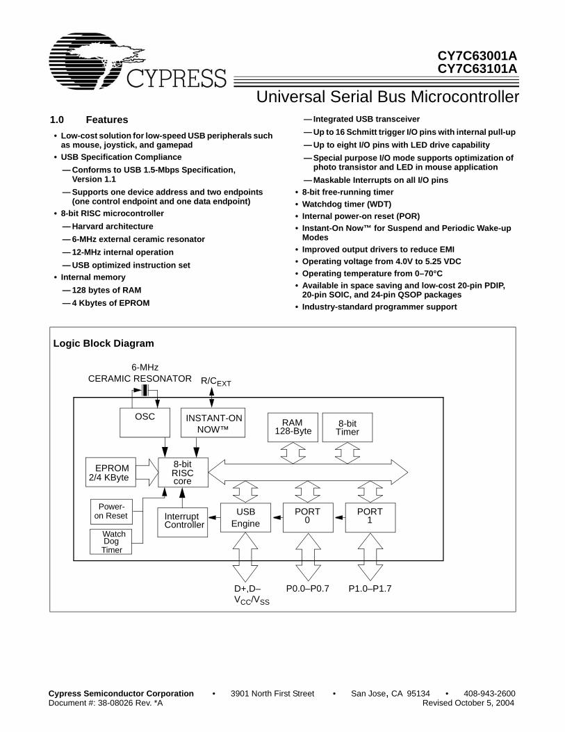
Universal Serial Bus Microcontroller CY7C63001A CY7C63101A Cypress Semiconductor Corporation • 3901 North First Street • San Jose, CA 95134 • 408-943-2600 Document #: 38-08026 Rev. *A Revised October 5, 2004 1.0 Features • Low-cost solution for low-speed USB peripherals such as mouse, joystick, and gamepad • USB Specification Compliance — Conforms to USB 1.5-Mbps Specification, Version 1.1 — Supports one device address and two endpoints (one control endpoint and one data endpoint) • 8-bit RISC microcontroller — Harvard architecture — 6-MHz external ceramic resonator — 12-MHz internal operation — USB optimized instruction set • Internal memory — 128 bytes of RAM — 4 Kbytes of EPROM — Integrated USB transceiver — Up to 16 Schmitt trigger I/O pins with internal pull-up —Up to eight I/O pins with LED drive capability —Special purpose I/O mode supports optimization of photo transistor and LED in mouse application — Maskable Interrupts on all I/O pins • 8-bit free-running timer • Watchdog timer (WDT) • Internal power-on reset (POR) • Instant-On Now™ for Suspend and Periodic Wake-up Modes • Improved output drivers to reduce EMI • Operating voltage from 4.0V to 5.25 VDC • Operating temperature from 0–70°C • Available in space saving and low-cost 20-pin PDIP, 20-pin SOIC, and 24-pin QSOP packages • Industry-standard programmer support 8-bit Timer Logic Block Diagram USB D+,D– PORT P0.0–P0.7 Interrupt Controller 0 PORT P1.0–P1.7 1 8-bit RISC OSC RAM 128-Byte EPROM 2/4 KByte core Power- on Reset Engine Watch Timer Dog 6-MHz CERAMIC RESONATOR INSTANT-ON NOW™ R/C EXT V CC /V SS
Transcript
Universal Serial Bus Microcontroller
CY7C63001ACY7C63101A
1.0 Features
• Low-cost solution for low-speed USB peripherals such as mouse, joystick, and gamepad
• USB Specification Compliance
— Conforms to USB 1.5-Mbps Specification, Version 1.1
— Supports one device address and two endpoints (one control endpoint and one data endpoint)
• 8-bit RISC microcontroller
— Harvard architecture
— 6-MHz external ceramic resonator
— 12-MHz internal operation
— USB optimized instruction set• Internal memory
— 128 bytes of RAM
— 4 Kbytes of EPROM
— Integrated USB transceiver
— Up to 16 Schmitt trigger I/O pins with internal pull-up
— Up to eight I/O pins with LED drive capability
— Special purpose I/O mode supports optimization of photo transistor and LED in mouse application
— Maskable Interrupts on all I/O pins• 8-bit free-running timer• Watchdog timer (WDT)• Internal power-on reset (POR)• Instant-On Now™ for Suspend and Periodic Wake-up
Modes• Improved output drivers to reduce EMI• Operating voltage from 4.0V to 5.25 VDC• Operating temperature from 0–70°C• Available in space saving and low-cost 20-pin PDIP,
20-pin SOIC, and 24-pin QSOP packages• Industry-standard programmer support
8-bitTimer
Logic Block Diagram
USB
D+,D–
PORT
P0.0–P0.7
InterruptController 0
PORT
P1.0–P1.7
1
8-bitRISC
OSCRAM
128-Byte
EPROM2/4 KByte core
Power-on Reset
EngineWatch
TimerDog
6-MHz CERAMIC RESONATOR
INSTANT-ONNOW™
R/CEXT
VCC/VSS
Cypress Semiconductor Corporation • 3901 North First Street • San Jose, CA 95134 • 408-943-2600Document #: 38-08026 Rev. *A Revised October 5, 2004
CY7C63001A CY7C63101A
2.0 Pin Configurations
3.0 Functional Overview
The CY7C630/101A is a family of 8-bit RISC One TimeProgrammable (OTP) microcontrollers with a built-in 1.5-MbpsUSB Serial Interface Engine (SIE). The microcontrollerfeatures 35 instructions that are optimized for USB applica-tions. In addition, the microcontroller features 128 bytes ofinternal RAM and four Kbytes of program memory space. TheCypress USB Controller accepts a 6-MHz ceramic resonatoras its clock source. This clock signal is doubled within the chipto provide a 12- MHz clock for the microprocessor.
The microcontroller features two ports of up to sixteen generalpurpose I/Os (GPIOs). Each GPIO pin can be used togenerate an interrupt to the microcontroller. Additionally, all
pins in Port 1 are equipped with programmable drivers strongenough to drive LEDs. The GPIO ports feature low EMIemissions as a result of controlled rise and fall times andunique output driver circuits. The Cypress microcontrollershave a range of GPIOs to fit various applications; theCY7C6300XA has twelve GPIOs and the CY7C6310XA hassixteen GPIOs. Notice that each part has eight ‘low-current’ports (Port 0) with the remaining ports (Port 1) being ‘high-current’ ports.
The 12-GPIO CY7C6300XA is available in 20-pin PDIP (-PC)and 20-pin SOIC (-SC) packages. The 26-GPIOCY7C6310XA is available in 24-pin QSOP (-QC) package.
1234567
9131415161718
2019
P0.0P0.1P0.2P0.3P1.0P1.2VSS
CEXT
P0.4
P1.1
P0.6P0.7
D+P1.3
D–VCC
DIP/SOIC
12
P0.5
8VPP
XTALIN XTALOUT10 11
123456
9
11
151617181920
2221
P0.0P0.1P0.2P0.3P1.0P1.2
VSS
CEXT
P0.6
P1.5
P1.1P1.3
D+P1.7
D–VCC
24-pin
14
P0.7
10VPP
XTALIN XTALOUT12 13
78
P1.4P1.6
2423
P0.4P0.5
SOIC/QSOP20-pin
CY7C63101A
8
567
DIE
4 3 2 1 24 23 22 21
17
201918
13 14 15 169 10 11 12
(Top View)
4.0 Pin Definitions
Name I/O 20-Pin 24-pin Die Pad # Description
P0.0 I/O 1 1 1 Port 0 bit 0
P0.1 I/O 2 2 2 Port 0 bit 1
P0.2 I/O 3 3 3 Port 0 bit 2
P0.3 I/O 4 4 4 Port 0 bit 3
P0.4 I/O 20 24 24 Port 0 bit 4
P0.5 I/O 19 23 23 Port 0 bit 5
P0.6 I/O 18 22 22 Port 0 bit 6
P0.7 I/O 17 21 21 Port 0 bit 7
P1.0 I/O 5 5 5 Port 1 bit 0
P1.1 I/O 16 20 20 Port 1 bit 1
P1.2 I/O 6 6 6 Port 1 bit 2
P1.3 I/O 15 19 19 Port 1 bit 3
P1.4 I/O – 7 7 Port 1 bit 4
P1.5 I/O – 18 18 Port 1 bit 5
P1.6 I/O – 8 8 Port 1 bit 6
P1.7 I/O – 17 17 Port 1 bit 7
XTALIN I 10 12 12 Ceramic resonator in
XTALOUT O 11 13 13 Ceramic resonator out
Document #: 38-08026 Rev. *A Page 2 of 25
CY7C63001A CY7C63101A
6.0 Functional Description
The Cypress CY7C630/101A USB microcontrollers areoptimized for human-interface computer peripherals such asa mouse, joystick, and gamepad. These USB microcontrollersconform to the low-speed (1.5 Mbps) requirements of the USBSpecification version 1.1. Each microcontroller is a self-contained unit with: a USB interface engine, USB transceivers,an 8-bit RISC microcontroller, a clock oscillator, timers, andprogram memory. Each microcontroller supports one USBdevice address and two endpoints.
The 6-MHz clock is doubled to 12 MHz to drive the microcon-troller. A RISC architecture with 35 instructions provides thebest balance between performance and product cost.
6.1 Memory OrganizationThe memory in the USB Controller is organized into userprogram memory in EPROM space and data memory in SRAMspace.
6.1.1 Program Memory Organization
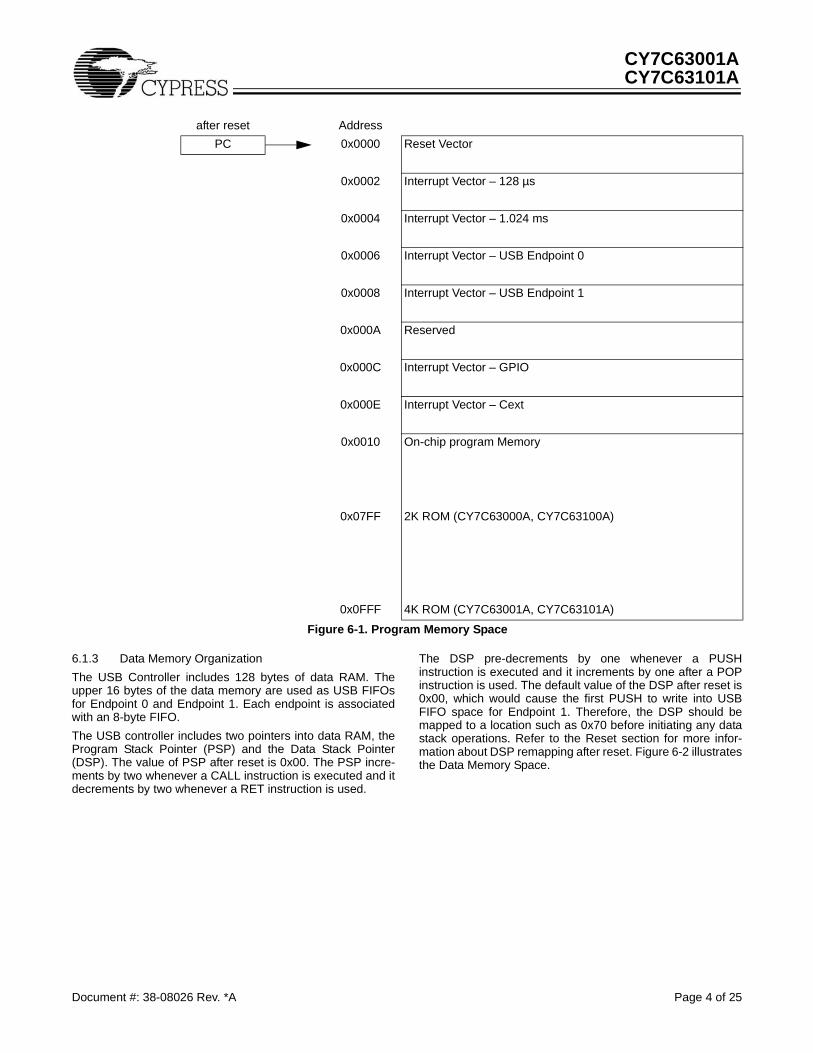
The CY7C63001A and CY7C63101A each offer 4 Kbytes ofEPROM. The program memory space is divided into twofunctional groups: interrupt vectors and program code.
The interrupt vectors occupy the first 16 bytes of the programspace. Each vector is 2 bytes long. After a reset, the ProgramCounter points to location zero of the program space. Figure6-1 shows the organization of the Program Memory Space.
6.1.2 Security Fuse Bit
The Cypress USB microcontroller includes a security fuse bit.When the security fuse is programmed, the EPROM programmemory outputs 0xFF to the EPROM programmer, thusprotecting the user’s code.
CEXT I/O 9 11 11 Connects to external R/C timing circuit for optional ‘suspend’ wakeup
D+ I/O 14 16 16 USB data+
D– I/O 13 15 15 USB data–
VPP – 8 10 10 Programming voltage supply, tie to ground during normal operation
VCC – 12 14 14 Voltage supply
VSS – 7 9 9 Ground
4.0 Pin Definitions (continued)
Name I/O 20-Pin 24-pin Die Pad # Description
5.0 Pin Description
Name Description
VCC One pin. Connects to the USB power source or to a nominal 5V power supply. Actual VCC range can vary between 4.0V and 5.25V.
VSS One pin. Connects to ground.
VPP One pin. Used in programming the on-chip EPROM. This pin should be tied to ground during normal opera-tions.
XTALIN One pin. Input from an external ceramic resonator.
XTALOUT One pin. Return path for the ceramic resonator (leave unconnected if driving XTALIN from an external oscillator).
P0.0–P0.7,P1.0–P1.7
Sixteen pins. P0.0–P0.7 are the 8 I/O lines in Port 0. P1.0–P1.7 are the 8 I/O lines in Port 1. P1.0–P1.3 are supported in the CY7C6300XA. All I/O pins include bit-programmable pull-up resistors. However, the sink current of each pin can be programmed to one of sixteen levels. Besides functioning as GPIO lines, each pin can be programmed as an interrupt input. The interrupt is edge-triggered, with programmable polarity.
D+, D– Two pins. Bidirectional USB data lines. An external pull-up resistor must be connected between the D pin and VCC to select low-speed USB operation.
CEXT One pin. Open-drain output with Schmitt trigger input. The input is connected to a rising edge-triggered interrupt. CEXT may be connected to an external RC to generate a wake-up from Suspend mode. See Section 6.4.
Document #: 38-08026 Rev. *A Page 3 of 25
CY7C63001A CY7C63101A
6.1.3 Data Memory Organization
The USB Controller includes 128 bytes of data RAM. Theupper 16 bytes of the data memory are used as USB FIFOsfor Endpoint 0 and Endpoint 1. Each endpoint is associatedwith an 8-byte FIFO.
The USB controller includes two pointers into data RAM, theProgram Stack Pointer (PSP) and the Data Stack Pointer(DSP). The value of PSP after reset is 0x00. The PSP incre-ments by two whenever a CALL instruction is executed and itdecrements by two whenever a RET instruction is used.
The DSP pre-decrements by one whenever a PUSHinstruction is executed and it increments by one after a POPinstruction is used. The default value of the DSP after reset is0x00, which would cause the first PUSH to write into USBFIFO space for Endpoint 1. Therefore, the DSP should bemapped to a location such as 0x70 before initiating any datastack operations. Refer to the Reset section for more infor-mation about DSP remapping after reset. Figure 6-2 illustratesthe Data Memory Space.
after reset Address
PC 0x0000 Reset Vector
0x0002 Interrupt Vector – 128 µs
0x0004 Interrupt Vector – 1.024 ms
0x0006 Interrupt Vector – USB Endpoint 0
0x0008 Interrupt Vector – USB Endpoint 1
0x000A Reserved
0x000C Interrupt Vector – GPIO
0x000E Interrupt Vector – Cext
0x0010 On-chip program Memory
0x07FF 2K ROM (CY7C63000A, CY7C63100A)
0x0FFF 4K ROM (CY7C63001A, CY7C63101A)
Figure 6-1. Program Memory Space
Document #: 38-08026 Rev. *A Page 4 of 25
CY7C63001A CY7C63101A
6.2 I/O Register SummaryI/O registers are accessed via the I/O Read (IORD) and I/OWrite (IOWR, IOWX) instructions.
after reset
Address
DSP PSP 0x00
userfirmware
0x02
0x04
DSP 0x70 USB FIFO – Endpoint 0
0x77
0x78 USB FIFO – Endpoint 1
0x7F
Figure 6-2. Data Memory Space
Table 6-1. I/O Register Summary
Register Name I/O Address Read/Write Function Page
P0 Data 0x00 R/W General purpose I/O Port (low current) Figure 6-8
P1 Data 0x01 R/W General purpose I/O Port (high current) Figure 6-9
P0 IE 0x04 W Interrupt enable for Port 0 pins Figure 6-17
P1 IE 0x05 W Interrupt enable for Port 1 pins Figure 6-18
P0 Pull-up 0x08 W Pull-up resistor control for Port 0 pins Figure 6-11
P1 Pull-up 0x09 W Pull-up resistor control for Port 1 pins Figure 6-12
USB SCR 0x13 R/W USB status and control Figure 6-24
EP0 RX Status 0x14 R/W USB Endpoint 0 receive status Figure 6-21
GIE 0x20 R/W Global Interrupt Enable Figure 6-15
WDT 0x21 W Watchdog Timer clear Figure 6-4
Cext 0x22 R/W External R-C Timing circuit control Figure 6-5
Timer 0x23 R Free-running timer Figure 6-6
P0 Isink 0x30-0x37 W Input sink current control for Port 0 pins. There is one Isink register for each pin. Address of the Isink register for pin 0 is located at 0x30 and the register address for pin 7 is located at 0x37.
Figure 6-13
Document #: 38-08026 Rev. *A Page 5 of 25
CY7C63001A CY7C63101A
6.3 ResetThe USB Controller supports three types of resets. Allregisters are restored to theirWatchdog default states during areset. The USB Device Address is set to 0 and all interruptsare disabled. In addition, the Program Stack Pointer (PSP) isset to 0x00 and the Data Stack Pointer (DSP) is set to 0x00.The user should set the DSP to a location such as 0x70 toreserve 16 bytes of USB FIFO space. The assembly instruc-tions to do so are:
MOV A, 70h ; Move 70 hex into Accumulator, use 70 instead of 6F because the dsp is
; always decremented by 1 before the data transfer of the PUSH instruction occursSWAP A, DSP ; Move Accumulator value into dsp
The three reset types are:
1. Power-On Reset (POR)
2. Watchdog Reset (WDR)
3. USB Reset
The occurrence of a reset is recorded in the Status and ControlRegister located at I/O address 0xFF (Figure 6-3). Readingand writing this register are supported by the IORD and IOWRinstructions. Bits 1, 2, and 7 are reserved and must be writtenas zeros during a write. During a read, reserved bit positionsshould be ignored. Bits 4, 5, and 6 are used to record theoccurrence of POR, USB, and WDR Reset respectively. Thefirmware can interrogate these bits to determine the cause ofa reset. If a Watchdog Reset occurs, firmware must clear theWDR bit (bit 6) in the Status and Control Register to re-enablethe USB transmitter (please refer to the Watchdog Resetsection for further details). Bit 0, the “Run” control, is set to 1at POR. Clearing this bit stops the microcontroller (firmwarenormally should not clear this bit). Once this bit is set to LOW,only a reset can set this bit HIGH.
The microcontroller resumes execution from ROM address0x00 after a reset unless the Suspend bit (bit 3) of the Statusand Control Register is set. Setting the Suspend bit stops theclock oscillator and the interrupt timers and powers down themicrocontroller. The detection of any USB activity, the occur-rence of a GPIO Interrupt, or the occurrence of the CextInterrupt terminates the suspend condition.
6.3.1 Power-On Reset
Power-On Reset (POR) occurs every time the power to thedevice is switched on. Bit 4 of the Status and Control Registeris set to record this event (the register contents are set to00011001 by the POR). The USB Controller is placed in
suspended mode at the end of POR to conserve power (theclock oscillator, the timers, and the interrupt logic are turnedoff in suspend mode). After POR, only a non-idle USB Busstate terminates the suspend mode. The microcontroller thenbegins execution from ROM address 0x00.
P1 Isink 0x38-0x3F W Input sink current control for Port 1 pins. There is one Isink register for each pin. Address of the Isink register for pin 0 is located at 0x38 and the register address for pin 7 is located at 0x3F. The number of Port 1 pins depends on package type.
Figure 6-13
SCR 0xFF R/W Processor status and control register Figure 6-3
Table 6-1. I/O Register Summary (continued)
Register Name I/O Address Read/Write Function Page
b7 b6 b5 b4 b3 b2 b1 b0
Reserved WDR USBR POR SUSPEND Reserved Reserved RUN
R/W R/W R/W R/W R/W
0 0 0 1 0 0 0 1
Figure 6-3. Status and Control Register (SCR – Address 0xFF)
Document #: 38-08026 Rev. *A Page 6 of 25
CY7C63001A CY7C63101A
6.3.2 Watchdog Reset (WDR)
The Watchdog Timer Reset (WDR) occurs when the MostSignificant Bit of the 4-bit Watchdog Timer Register transitionsfrom LOW to HIGH. Writing any value to the write-onlyWatchdog Restart Register at 0x21 clears the timer (firmwareshould periodically write to the Watchdog Restart Register inthe ‘main loop’ of firmware). The Watchdog timer is clocked bya 1.024-ms clock from the free-running timer. If 8 clocks occurbetween writes to the timer, a WDR occurs and bit 6 of theStatus and Control Register is set to record the event. AWatchdog Timer Reset lasts for 8.192 ms, at which time themicrocontroller begins execution at ROM address 0x00. TheUSB transmitter is disabled by a Watchdog Reset because theUSB Device Address Register is cleared (otherwise, the USBController would respond to all address 0 transactions). Thetransmitter remains disabled until the WDR bit (bit 6) in theStatus and Control Register is reset to 0 by firmware.
6.3.3 USB Bus Reset
The USB Controller recognizes a USB Reset when a SingleEnded Zero (SE0) condition persists for at least 8–16 µs (theReset may be recognized for an SE0 as short as 8 µs, but it isalways recognized for an SE0 longer than 16 µs). SE0 is thecondition in which both the D+ line and the D– line are LOW.Bit 5 of the Status and Control Register is set to record thisevent. If the USB reset happens while the device issuspended, the suspend condition is cleared and the clockoscillator is restarted. However, the microcontroller is notreleased until the USB reset is removed.
6.4 Instant-on Feature (Suspend Mode)The USB Controller can be placed in a low-power state bysetting the Suspend bit (bit 3) of the Status and Control
register. All logic blocks in the device are turned off except theUSB receiver, the GPIO interrupt logic, and the Cext interruptlogic. The clock oscillator and the free-running and Watchdogtimers are shut down.
The suspend mode is terminated when one of the followingthree conditions occur:
1. USB activity
2. A GPIO interrupt
3. Cext interrupt
The clock oscillator, GPIO, and timers restart immediatelyupon exiting suspend mode. The USB engine and microcon-troller return to a fully functional state no more than 256 µslater. Before servicing any interrupt requests, the microcon-troller executes the instruction following the I/O write thatplaced the device into suspend mode.
Both the GPIO interrupt and the Cext interrupt allow the USBController to wake-up periodically and poll potentiometers,optics, and other system components while maintaining a verylow average power consumption. The Cext Interrupt ispreferred for lowest power consumption.
For Cext to generate an “Instant-on” interrupt, the pin must beconnected to ground with an external capacitor and connectedto VCC with an external resistor. A “0” is written to the Cextregister located at I/O address 0x22 to discharge the capacitor.Then, a “1” is written to disable the open-drain output driver. ASchmitt trigger input circuit monitors the input and generatesa wake-up interrupt when the input voltage rises above theinput threshold. By changing the values of the external resistorand capacitor, the user can fine tune the charge rate of the R-C timing circuit. The format of the Cext register is shown inFigure 6-5. Reading the register returns the value of the Cextpin. During a reset, the Cext pin is HIGH.
6.5 On-Chip TimerThe USB Controller is equipped with a free-running timerdriven by a clock one-sixth the resonator frequency. Bits 0through 7 of the counter are readable from the read-only TimerRegister located at I/O address 0x23. The Timer Register iscleared during a Power-On Reset and whenever Suspend
mode is entered. Figure 6-6 illustrates the format of thisregister and Figure 6-7 is its block diagram.
With a 6 MHz resonator, the timer resolution is 1 µs.
The timer generates two interrupts: the 128-µs interrupt andthe 1.024-ms interrupt.
6.6 General Purpose I/O PortsInterface with peripherals is conducted via as many as 16GPIO signals. These signals are divided into two ports: Port 0and Port 1. Port 0 contains eight lines (P0.0–P0.7) and Port 1contains up to eight lines (P1.0–P1.7). The number of externalI/O pins depends on the package type. Both ports can beaccessed by the IORD, IOWR, and IOWX instructions. The
Port 0 data register is located at I/O address 0x00 while thePort 1 data register is located at I/O address 0x01. Thecontents of both registers are set HIGH during a reset. Referto Figures 6-8 and 6-9 for the formats of the data registers. Inaddition to supporting general input/output functions, each I/Oline can trigger an interrupt to the microcontroller. Please referto the interrupt section for more details.
Figure 6-6. Timer Register (Address 0x23)
b7 b6 b5 b4 b3 b2 b1 b0
T.7 T.6 T.5 T.4 T.3 T.2 T.1 T.0
R R R R R R R R
0 0 0 0 0 0 0 0
Figure 6-7. Timer Block Diagram
9 78 56 4 3 2 1 0Resonator Clock/6
1.024-ms interrupt
128-ms interrupt
To Timer Register
8
b7 b6 b5 b4 b3 b2 b1 b0
P0.7 P0.6 P0.5 P0.4 P0.3 P0.2 P0.1 P0.0
R/W R/W R/W R/W R/W R/W R/W R/W
1 1 1 1 1 1 1 1
Figure 6-8. Port 0 Data Register (Address 0x00)
b7 b6 b5 b4 b3 b2 b1 b0
P1.7 P1.6 P1.5 P1.4 P1.3 P1.2 P1.1 P1.0
R/W R/W R/W R/W R/W R/W R/W R/W
1 1 1 1 1 1 1 1
Figure 6-9. Port 1 Data Register (Address 0x01)
Document #: 38-08026 Rev. *A Page 8 of 25
CY7C63001A CY7C63101A
Each GPIO line includes an internal Rup resistor. This resistorprovides both the pull-up function and slew control. Twofactors govern the enabling and disabling of each resistor: thestate of its associated Port Pull-up register bit and the state ofthe Data Register bit. NOTE: The control bits in the Port Pull-up register are active LOW.
A GPIO line is HIGH when a “1” is written to the Data Registerand a “0” is written to the respective Port Pull-up register.Writing a “0” to the port Data Register disables the port’s Pull-up resistor and outputs a LOW on the GPIO line regardless ofthe setting in the Port Pull-up Register. The output goes to ahigh-Z state if the Data Register bit and the Port Pull-upRegister bit are both “1”. Figure 6-10 illustrates the block
diagram of one I/O line. The Port Isink Register is used tocontrol the output current level and it is described later in thissection. NOTE: The Isink logic block is turned off duringsuspend mode (please refer to the Instant-on Feature sectionfor more details). Therefore, to prevent higher ICC currentsduring USB suspend mode, firmware must set ALL Port 0 andPort 1 Data Register bits (which are not externally driven to aknown state), including those that are not bonded out on aparticular package, to “1” and all Port 0 and Port 1 Pull-UpRegister data bits to “0” to enable port pull-ups before settingthe Suspend bit (bit 3 of the Status and Control Register).Table 6-2 is the Output Control truth table.
To configure a GPIO pin as an input, a “1” should be written tothe Port Data Register bit associated with that pin to disablethe pull-down function of the Isink DAC (see Figure 6-10).When the Port Data Register is read, the bit value is a “1”if the voltage on the pin is greater than the Schmitt triggerthreshold, or “0” if it is below the threshold. In applicationswhere an internal pull-up is required, the Rup pull-up resistorcan be engaged by writing a “0” to the appropriate bit in thePort Pull-up Register.
Both Port 0 and Port 1 Pull-up Registers are write only (seeFigures 6-11 and 6-12). The Port 0 Pull-up Register is locatedat I/O address 0x08 and Port 1 Pull-up Register is mapped toaddress 0x09. The contents of the Port Pull-up Registers arecleared during reset, allowing the outputs to be controlled bythe state of the Data Registers. The Port Pull-up Registers alsoselect the polarity of transition that generates a GPIO interrupt.A “0” selects a HIGH to LOW transition while a “1” selects aLOW to HIGH transition.
Figure 6-10. Block Diagram of an I/O Line
Table 6-2. Output Control Truth Table
Data Register Port Pull-up Register Output at I/O Pin Interrupt Polarity
Figure 6-11. Port 0 Pull-up Register (Address 0x08)
Document #: 38-08026 Rev. *A Page 9 of 25
CY7C63001A CY7C63101A
Writing a “0” to the Data Register drives the output LOW.Instead of providing a fixed output drive, the USB Controllerallows the user to select an output sink current level for eachI/O pin. The sink current of each output is controlled by a
dedicated Port Isink Register. The lower four bits of thisregister contain a code selecting one of sixteen sink currentlevels. The upper four bits of the register are ignored. Theformat of the Port Isink Register is shown in Figure 6-13.
Port 0 is a low-current port suitable for connecting phototransistors. Port 1 is a high current port capable of drivingLEDs. See section 8.0 for current ranges. 0000 is the lowestdrive strength. 1111 is the highest.
The write-only sink current control registers for Port 0 outputsare assigned from I/O address 0x30 to 0x37 with the controlbits for P00 starting at 0x30. Port 1 sink current controlregisters are assigned from I/O address 0x38 to 0x3F with thecontrol bits for P10 starting at 0x38. All sink current control
registers are cleared during a reset, resulting in the minimumcurrent sink setting.
6.7 XTALIN/XTALOUTThe XTALIN and XTALOUT pins support connection of a 6-MHz ceramic resonator. The feedback capacitors and biasresistor are internal to the IC, as shown in Figure 6-14 LeaveXTALOUT unconnected when driving XTALIN from an externaloscillator.
6.8 InterruptsInterrupts are generated by the General Purpose I/O lines, theCext pin, the internal timer, and the USB engine. All interruptsare maskable by the Global Interrupt Enable Register. Accessto this register is accomplished via IORD, IOWR, and IOWX
instructions to address 0x20. Writing a “1” to a bit positionenables the interrupt associated with that position. During areset, the contents of the Interrupt Enable Register arecleared, disabling all interrupts. Figure 6-15 illustrates theformat of the Global Interrupt Enable Register.
The interrupt controller contains a separate latch for eachinterrupt. See Figure 6-16 for the logic block diagram for theinterrupt controller. When an interrupt is generated, it islatched as a pending interrupt. It stays as a pending interruptuntil it is serviced or a reset occurs. A pending interrupt only
generates an interrupt request if it is enabled in the GlobalInterrupt Enable Register. The highest priority interruptrequest is serviced following the execution of the currentinstruction.
Figure 6-15. Global Interrupt Enable Register (GIER – Address 0x20)
Document #: 38-08026 Rev. *A Page 10 of 25
CY7C63001A CY7C63101A
When servicing an interrupt, the hardware first disables allinterrupts by clearing the Global Interrupt Enable Register.Next, the interrupt latch of the current interrupt is cleared. Thisis followed by a CALL instruction to the ROM addressassociated with the interrupt being serviced (i.e., the interruptvector). The instruction in the interrupt table is typically a JMPinstruction to the address of the Interrupt Service Routine(ISR). The user can re-enable interrupts in the interrupt serviceroutine by writing to the appropriate bits in the Global InterruptEnable Register. Interrupts can be nested to a level limitedonly by the available stack space.
The Program Counter (PC) value and the Carry and Zero flags(CF, ZF) are automatically stored onto the Program Stack bythe CALL instruction as part of the interrupt acknowledge
process. The user firmware is responsible for ensuring that theprocessor state is preserved and restored during an interrupt.For example the PUSH A instruction should be used as thefirst command in the ISR to save the accumulator value. And,the IPRET instruction should be used to exit the ISR with theaccumulator value restored and interrupts enabled. The PC,CF, and ZF are restored when the IPRET or RET instructionsare executed.
The Interrupt Vectors supported by the USB Controller arelisted in Table 6-3. Interrupt Vector 0 (Reset) has the highestpriority, Interrupt Vector 7 has the lowest priority. Because theJMP instruction is two bytes long, the interrupt vectors occupytwo bytes.
6.8.1 Interrupt Latency
Interrupt latency can be calculated from the followingequation:
Interrupt Latency = (Number of clock cycles remaining in thecurrent instruction) + (10 clock cycles forthe CALL instruction) + (5 clock cyclesfor the JMP instruction)
For example, if a 5-clock-cycle instruction such as JC is beingexecuted when an interrupt occurs, the first instruction of theInterrupt Service Routine executes a minimum of 16 clockcycles (1+10+5) or a maximum of 20 clock cycles (5+10+5)after the interrupt is issued. Therefore, the interrupt latency inthis example will be = 20 clock periods = 20 / (12 MHz) = 1.667µs. The interrupt latches are sampled at the rising edge of thelast clock cycle in the current instruction.
The General Purpose I/O interrupts are generated by signaltransitions at the Port 0 and Port 1 I/O pins. GPIO interruptsare edge sensitive with programmable interrupt polarities.Setting a bit HIGH in the Port Pull-up Register (see Figure 6-11 and 6-12) selects a LOW to HIGH interrupt trigger for thecorresponding port pin. Setting a bit LOW activates a HIGH to
LOW interrupt trigger. Each GPIO interrupt is maskable on aper-pin basis by a dedicated bit in the Port Interrupt EnableRegister. Writing a “1” enables the interrupt. Figure 6-17 andFigure 6-18 illustrate the format of the Port Interrupt EnableRegisters for Port 0 and Port 1 located at I/O address 0x04 and0x05 respectively. These write only registers are clearedduring reset, thus disabling all GPIO interrupts.
A block diagram of the GPIO interrupt logic is shown in Figure6-19. The bit setting in the Port Pull-up Register selects theinterrupt polarity. If the selected signal polarity is detected onthe I/O pin, a HIGH signal is generated. If the Port InterruptEnable bit for this pin is HIGH and no other port pins arerequesting interrupts, the OR gate issues a LOW to HIGH
signal to clock the GPIO interrupt flip-flop. The output of theflip-flop is further qualified by the Global GPIO Interrupt Enablebit before it is processed by the Interrupt Priority Encoder. Boththe GPIO interrupt flip-flop and the Global GPIO Enable bit arecleared by on-chip hardware during GPIO interruptacknowledge.
Note. If one port pin triggers an interrupt, no other port pin cancause a GPIO interrupt until the port pin that triggered theinterrupt has returned to its inactive (non-trigger) state or untilits corresponding port interrupt enable bit is cleared (theseevents ‘reset’ the clock of the GPIO Interrupt flip-flop, whichmust be ‘reset’ to ‘0’ before another GPIO interrupt event can‘clock’ the GPIO Interrupt flip-flop and produce an IRQ).
Note. If the port pin that triggered an interrupt is held in itsactive (trigger) state while its corresponding port interrupt
enable bit is cleared and then set, a GPIO interrupt eventoccurs as the GPIO Interrupt flip-flop clock transitions from ‘1’to ‘0’ and then back to ‘1’ (please refer to Figure 6-19). TheUSB Controller does not assign interrupt priority to differentport pins and the Port Interrupt Enable Registers are notcleared during the interrupt acknowledge process. When aGPIO interrupt is serviced, the ISR must poll the ports todetermine which pin caused the interrupt.
A USB Endpoint 0 interrupt is generated after the host haswritten data to Endpoint 0 or after the USB Controller hastransmitted a packet from Endpoint 0 and receives an ACKfrom the host. An OUT packet from the host which is NAKedby the USB Controller does not generate an interrupt. Thisinterrupt is masked by the USB EP0 Interrupt Enable bit (bit 3)of the Global Interrupt Enable Register.
A USB Endpoint 1 interrupt is generated after the USBController has transmitted a packet from Endpoint 1 and hasreceived an ACK from the host. This interrupt is masked by theUSB EP1 Interrupt Enable bit (bit 4) of the Global InterruptEnable Register.
6.8.4 Timer Interrupt
There are two timer interrupts: the 128-µs interrupt and the1.024-ms interrupt. They are masked by bits 1 and 2 of theGlobal Interrupt Enable Register respectively. The user shoulddisable both timer interrupts before going into the suspendmode to avoid possible conflicts from timer interrupts occurringjust as suspend mode is entered.
6.8.5 Wake-Up Interrupt
A wake-up interrupt is generated when the Cext pin goesHIGH. This interrupt is latched in the interrupt controller. It canbe masked by the Wake-up Interrupt Enable bit (bit 7) of theGlobal Interrupt Enable Register. This interrupt can be used toperform periodic checks on attached peripherals when theUSB Controller is placed in the low-power suspend mode. Seethe Instant-On Feature section for more details.
6.9 USB EngineThe USB engine includes the Serial Interface Engine (SIE)and the low-speed USB I/O transceivers. The SIE blockperforms most of the USB interface functions with only minimalsupport from the microcontroller core. Two endpoints aresupported. Endpoint 0 is used to receive and transmit control(including setup) packets while Endpoint 1 is only used totransmit data packets.
The USB SIE processes USB bus activity at the transactionlevel independently. It does all the NRZI encoding/decodingand bit stuffing/unstuffing. It also determines token type,checks address and endpoint values, generates and checksCRC values, and controls the flow of data bytes between thebus and the Endpoint FIFOs. NOTE: the SIE stalls the CPU forthree cycles per byte when writing data to the endpoint FIFOs(or 3 * 1/12 MHz * 8 bytes = 2 µs per 8-byte transfer).
The firmware handles higher level and function-specific tasks.During control transfers the firmware must interpret devicerequests and respond correctly. It also must coordinateSuspend/Resume, verify and select DATA toggle values, andperform function specific tasks.
The USB engine and the firmware communicate though theEndpoint FIFOs, USB Endpoint interrupts, and the USBregisters described in the sections below.
6.9.1 USB Enumeration Process
The USB Controller provides a USB Device Address Registerat I/O location 0x12. Reading and writing this register isachieved via the IORD and IOWR instructions. The registercontents are cleared during a reset, setting the USB addressof the USB Controller to 0. Figure 6-20 shows the format of theUSB Address Register.
Typical enumeration steps:
1. The host computer sends a SETUP packet followed by a DATA packet to USB address 0 requesting the Device descriptor.
2. The USB Controller decodes the request and retrieves its Device descriptor from the program memory space.
3. The host computer performs a control read sequence and the USB Controller responds by sending the Device descriptor over the USB bus.
4. After receiving the descriptor, the host computer sends a SETUP packet followed by a DATA packet to address 0 assigning a new USB address to the device.
5. The USB Controller stores the new address in its USB Device Address Register after the no-data control sequence completes.
6. The host sends a request for the Device descriptor using the new USB address.
7. The USB Controller decodes the request and retrieves the Device descriptor from the program memory.
8. The host performs a control read sequence and the USB Controller responds by sending its Device descriptor over the USB bus.
9. The host generates control reads to the USB Controller to request the Configuration and Report descriptors.
10.The USB Controller retrieves the descriptors from its program space and returns the data to the host over the USB.
11.Enumeration is complete after the host has received all the descriptors.
b7 b6 b5 b4 b3 b2 b1 b0
Reserved ADR6 ADR5 ADR4 ADR3 ADR2 ADR1 ADR0
R/W R/W R/W R/W R/W R/W R/W
0 0 0 0 0 0 0 0
Figure 6-20. USB Device Address Register (USB DA – Address 0x12)
Document #: 38-08026 Rev. *A Page 13 of 25
CY7C63001A CY7C63101A
6.9.2 Endpoint 0
All USB devices are required to have an endpoint number 0that is used to initialize and manipulate the device. Endpoint 0provides access to the device’s configuration information andallows generic USB status and control accesses.
Endpoint 0 can receive and transmit data. Both receive andtransmit data share the same 8-byte Endpoint 0 FIFO locatedat data memory space 0x70 to 0x77. Received data mayoverwrite the data previously in the FIFO.
6.9.2.1 Endpoint 0 Receive
After receiving a packet and placing the data into the Endpoint0 FIFO, the USB Controller updates the USB Endpoint 0 RXregister to record the receive status and then generates a USBEndpoint 0 interrupt. The format of the Endpoint 0 RX Registeris shown in Figure 6-21.
This is a read/write register located at I/O address 0x14. Anywrite to this register clears all bits except bit 3 which remainsunchanged. All bits are cleared during reset.
Bit 0 is set to 1 when a SETUP token for Endpoint 0 is received.Once set to a 1, this bit remains HIGH until it is cleared by anI/O write or a reset. While the data following a SETUP is beingreceived by the USB engine, this bit is not cleared by an I/Owrite. User firmware writes to the USB FIFOs are disabledwhen bit 0 is set. This prevents SETUP data from beingoverwritten.
Bits 1 and 2 are updated whenever a valid token is receivedon Endpoint 0. Bit 1 is set to 1 if an OUT token is received andcleared to 0 if any other token is received. Bit 2 is set to 1 if anIN token is received and cleared to 0 if any other token isreceived.
Bit 3 shows the Data Toggle status of DATA packets receivedon Endpoint 0. This bit is updated for DATA following SETUPtokens and for DATA following OUT tokens if Stall (bit 5 of0x10) is not set and either EnableOuts or StatusOuts (bits 3and 4 of 0x13) are set.
Bits 4 to 7 are the count of the number of bytes received in aDATA packet. The two CRC bytes are included in the count,so the count value is two greater than the number of data bytes
received. The count is always updated and the data is alwaysstored in the FIFO for DATA packets following a SETUP token.The count for DATA following an OUT token is updated if Stall(bit 5 of 0x10) is 0 and either EnableOuts or StatusOuts (bits3 and 4 of 0x13) are 1. The DATA following an OUT is writteninto the FIFO if EnableOuts is set to 1 and Stall and StatusOutsare 0.
A maximum of eight bytes are written into the Endpoint 0 FIFO.If there are less than eight bytes of data the CRC is written intothe FIFO.
Due to register space limitations, the Receive Data Invalid bitis located in the USB Endpoint 0 TX Configuration Register.Refer to the Endpoint 0 Transmit section for details. This bit isset by the SIE if an error is detected in a received DATA packet.
Table 6-4 summarizes the USB Engine response to SETUPand OUT transactions on Endpoint 0. In the Data Packetcolumn ‘Error’ represents a packet with a CRC, PID or bit-stuffing error, or a packet with more than eight bytes of data.‘Valid’ is a packet without an Error. ‘Status’ is a packet that isa valid control read Status stage, while ‘N/Status’ is not acorrect Status stage (see section 6.9.4). The ‘Stall’ bit isdescribed in Section 6.9.2.2. The ‘StatusOuts’ and‘EnableOuts’ bits are described in section 6.9.4.
b7 b6 b5 b4 b3 b2 b1 b0
COUNT3 COUNT2 COUNT1 COUNT0 TOGGLE IN OUT SETUP
R/W R/W R/W R/W R R/W R/W R/W
0 0 0 0 0 0 0 0
Figure 6-21. USB Endpoint 0 RX Register (Address 0x14)
Table 6-4. USB Engine Response to SETUP and OUT Transactions on Endpoint 0
Control Bit Settings Received Packets USB Engine Response
Stall Status Out Enable OutToken Type
Data Packet FIFO Write
ToggleUpdate
CountUpdate Interrupt Reply
– – – SETUP Valid Yes Yes Yes Yes ACK
– – – SETUP Error Yes Yes Yes Yes None
0 0 1 OUT Valid Yes Yes Yes Yes ACK
0 0 1 OUT Error Yes Yes Yes Yes None
0 0 0 OUT Valid No No No No NAK
0 0 0 OUT Error No No No No None
1 0 0 OUT Valid No No No No STALL
1 0 0 OUT Error No No No No None
0 1 0 OUT Status No Yes Yes Yes ACK
0 1 0 OUT N/Status No Yes Yes Yes STALL
0 1 0 OUT Error No Yes No No None
Document #: 38-08026 Rev. *A Page 14 of 25
CY7C63001A CY7C63101A
6.9.2.2 Endpoint 0 Transmit
The USB Endpoint 0 TX Register located at I/O address 0x10controls data transmission from Endpoint 0 (see Figure 6-22).This is a read/write register. All bits are cleared during reset.
Bits 0 to 3 indicate the numbers of data bytes to be transmittedduring an IN packet, valid values are 0 to 8 inclusive. Bit 4indicates that a received DATA packet error (CRC, PID, orbitstuffing error) occurred during a SETUP or OUT data phase.Setting the Stall bit (bit 5) stalls IN and OUT packets. This bitis cleared whenever a SETUP packet is received byEndpoint 0. Bit 6 (Data 1/0) must be set to 0 or 1 to select theDATA packet’s toggle state (0 for DATA0, 1 for DATA1).
After the transmit data has been loaded into the FIFO, bit 6should be set according to the data toggle state and bit 7 setto “1”. This enables the USB Controller to respond to an INpacket. Bit 7 is cleared and an Endpoint 0 interrupt isgenerated by the SIE once the host acknowledges the datatransmission. Bit 7 is also cleared when a SETUP token is
received. The Interrupt Service Routine can check bit 7 toconfirm that the data transfer was successful.
6.9.3 Endpoint 1
Endpoint 1 is capable of transmit only. The data to be trans-mitted is stored in the 8-byte Endpoint 1 FIFO located at datamemory space 0x78 to 0x7F.
6.9.3.1 Endpoint 1 Transmit
Transmission is controlled by the USB Endpoint 1 TX Registerlocated at I/O address 0x11 (see Figure 6-23). This is aread/write register. All bits are cleared during reset.
Bits 0 to 3 indicate the numbers of data bytes to be transmittedduring an IN packet, valid values are 0 to 8 inclusive.
Bit 4 must be set before Endpoint 1 can be used. If this bit iscleared, the USB Controller ignores all traffic to Endpoint 1.
Setting the Stall bit (bit 5) stalls IN and OUT packets until thisbit is cleared.
Bit 6 (Data 1/0) must be set to either 0 or 1 depending on thedata packet’s toggle state, 0 for DATA0, 1 for DATA1.
After the transmit data has been loaded into the FIFO, bit 6should be set according to the data toggle state and bit 7 set
to “1”. This enables the USB Controller to respond to an INpacket. Bit 7 is cleared and an Endpoint 1 interrupt isgenerated by the SIE once the host acknowledges the datatransmission.
6.9.4 USB Status and Control
USB status and control is regulated by USB Status and ControlRegister located at I/O address 0x13 as shown in Figure 6-24.This is a read/write register. All reserved bits must be writtento zero. All bits in the register are cleared during reset.
Bit 0 is set by the SIE if any USB activity except idle (D+ LOW,D– HIGH) is detected. The user program should check andclear this bit periodically to detect any loss of bus activity.Writing a 0 to this bit clears it. Writing a 1 does not change itsvalue.
Bit 1 is used to force the on-chip USB transmitter to the K statewhich sends a Resume signal to the host. Bit 2 is used to forcethe transmitter to the J state. This bit should normally be set to
zero. However, for resume signaling, force a J state for oneinstruction before forcing resume.
Bit 3 is used to automatically respond to the Status stage OUTof a control read transfer on Endpoint 0. A valid Status stageOUT contains a DATA1 packet with 0 bytes of data. If the Statu-sOuts bit is set, the USB engine responds to a valid Statusstage OUT with an ACK, and any other OUT with a STALL.
b7 b6 b5 b4 b3 b2 b1 b0
INEN DATA1/0 STALL ERR COUNT3 COUNT2 COUNT1 COUNT0
R/W R/W R/W R/W R/W R/W R/W R/W
0 0 0 0 0 0 0 0
Figure 6-22. USB Endpoint 0 TX Configuration Register (Address 0x10)
b7 b6 b5 b4 b3 b2 b1 b0
INEN DATA1/0 STALL EP1EN COUNT3 COUNT2 COUNT1 COUNT0
R/W R/W R/W R/W R/W R/W R/W R/W
0 0 0 0 0 0 0 0
Figure 6-23. USB Endpoint 1 TX Configuration Register (Address 0x11)
Figure 6-24. USB Status and Control Register (USB SCR – Address 0x13)
Document #: 38-08026 Rev. *A Page 15 of 25
CY7C63001A CY7C63101A
The data is not written into the FIFO when this bit is set. Thisbit is cleared when a SETUP token is received by Endpoint 0.
Bit 4 is used to enable the receiving of Endpoint 0 OUTpackets. When this bit is set to 1, the data from an OUT trans-action is written into the Endpoint 0 FIFO. If this bit is 0, datais not written to the FIFO and the SIE responds with a NAK.This bit is cleared following a SETUP or ACKed OUT trans-action. Note. After firmware decodes a SETUP packet andprepares for a subsequent OUT transaction by setting bit 4, bit4 is not cleared until the hand-shake phase of an ACKed OUTtransaction (a NAKed OUT transaction does not clear this bit).
6.10 USB Physical Layer CharacteristicsThe following section describes the CY7C630/101Acompliance to the Chapter 7 Electrical section of the USBSpecification, Revision 1.1. The section contains all signaling,power distribution, and physical layer specifications necessaryto describe a low- speed USB function.
6.10.1 Low-Speed Driver Characteristics
The CY7C630/101A devices use a differential output driver todrive the Low-speed USB data signal onto the USB cable, asshown in Figure 6-25. The output swings between the differ-ential HIGH and LOW state are well balanced to minimizesignal skew. Slew rate control on the driver minimizes theradiated noise and cross talk on the USB cable. The driver’soutputs support three-state operation to achieve bidirectionalhalf duplex operation. The CY7C630/101A driver tolerates avoltage on the signal pins of –0.5V to 3.8V with respect to localground reference without damage. The driver tolerates thisvoltage for 10.0 µs while the driver is active and driving, andtolerates this condition indefinitely when the driver is in its high-impedance state.
A low-speed USB connection is made through an unshielded,untwisted wire cable a maximum of three meters in length. Therise and fall time of the signals on this cable are well controlledto reduce RFI emissions while limiting delays, signaling skewsand distortions. The CY7C630/101A driver reaches thespecified static signal levels with smooth rise and fall times,resulting in minimal reflections and ringing when driving theUSB cable. This cable and driver are intended to be used onlyon network segments between low-speed devices and theports to which they are connected.
6.10.2 Receiver Characteristics
The CY7C630/101A has a differential input receiver which isable to accept the USB data signal. The receiver features aninput sensitivity of at least 200 mV when both differential datainputs are in the range of at least 0.8V to 2.5V with respect toits local ground reference. This is the common mode inputvoltage range. Proper data reception is also guaranteed when
the differential data lines are outside the common mode range,as shown in Figure 6-26. The receiver tolerates static inputvoltages between –0.5V and 3.8V with respect to its localground reference without damage. In addition to the differ-ential receiver, there is a single-ended receiver for each of thetwo data lines. The single-ended receivers have a switchingthreshold between 0.8V and 2.0V (TTL inputs).
Figure 6-25. Low-speed Driver Signal Waveforms
VSS
Signal pinspass outputspec levels
with minimalreflections and
ringing
One BitTime
(1.5Mb/s)
DriverSignal Pins
VSE (max)
VSE (min)
Document #: 38-08026 Rev. *A Page 16 of 25
CY7C63001A CY7C63101A
6.11 External USB Pull-Up ResistorThe USB system specifies that a pull-up resistor be connectedon the D– pin of low-speed peripherals as shown in Figure 6-27. To meet the USB 1.1 spec (section 7.1.6), which states thatthe termination must charge the D– line from 0 to 2.0 V in2.5 µs, the total load capacitance on the D+/D– lines of thelow-speed USB device (Cypress device capacitance + PCB
trace capacitance + integrated cable capacitance) must beless than 250 pF. As Cypress D+/D– transceiver input capac-itance is 20pF max, up to 230 pF of capacitance is allowed forin the low speed device’s integrated cable and PCB. If thecable + PCB capacitance on the D+/D– lines will be greaterthan approximately 230 pF, an external 3.3V regulator must beused as shown in Figure 6-28.
Figure 6-26. Differential Input Sensitivity Over Entire Common Mode Range
tVCCS VCC Slew Linear ramp on VCC pin to VCC[3, 4] 0.010 1000 ms
USB Interface
Voh Static Output High 15kΩ ± 5% to Gnd[5,6] 2.8 3.6 V
Vol Static Output Low See Notes 5 and 6 0.3 V
Vdi Differential Input Sensitivity |(D+)–(D–)|, and Figure 6-26 0.2 V
Vcm Differential Input Common Mode Range Figure 6-26 0.8 2.5 V
Vse Single Ended Receiver Threshold 0.8 2.0 V
Cin Transceiver Input Capacitance D+ to Vss; D- to Vss 20 pF
Ilo Data Line (D+, D–) Leakage 0 V <(D+, D–)<3.3 V, Hi-Z State –10 10 µA
Rpu1 External Bus Pull-up Resistance, D– pin 1.5 kΩ ± 5% to 3.3V supply 1.425 1.575 kΩRpu2 External Bus Pull-up Resistance, D– pin 7.5 kΩ ± 1% to Vcc[7] 7.425 7.575 kΩRpd External Bus Pull-down Resistance 15 kΩ ± 5% 14.25 15.75 kΩ
General Purpose I/O Interface
Rup Pull-up Resistance 8 24 kΩIsink0(0) Port 0 Sink Current (0), lowest current Vout = 2.0V DC, Port 0 only[5] 0.1 0.3 mA
Isink0(F) Port 0 Sink Current (F), highest current Vout = 2.0V DC, Port 0 only[5] 0.5 1.5 mA
Isink1(0) Port 1 Sink Current (0), lowest current Vout = 2.0V DC, Port 1 only[5] 1.6 4.8 mA
Isink1(F) Port 1 Sink Current (F), highest current Vout = 2.0V DC, Port 1 only[5]
Vout = 0.4V DC, Port 1 only[5]85
24 mAmA
Irange Sink Current max./min. Vout = 2.0V DC, Port 0 or 1[5, 8] 4.5 5.5
Ilin Differential Nonlinearity Port 0 or Port 1[11] 0.5 lSB
Tratio Tracking Ratio Port1 to Port0 Vout = 2.0V[12] 14.4 19.6
tsink Current Sink Response Time Full scale transition 0.8 µs
Imax Port 1 Max Sink Current Summed over all Port 1 bits 60 mANotes:1. All pins specified for >200 mA positive and negative injection, except P1.0 is specified for >50 mA negative injection.2. Cext at VCC or Gnd, Port 0 and Port1 at VCC.3. Part powers up in suspend mode, able to be reset by USB Bus Reset.4. POR may re-occur whenever VCC drops to approximately 2.5V.5. Level guaranteed for range of VCC = 4.35V to 5.25V.6. With Rpu1 of 1.5 KW±5% on D– to 3.3V regulator. 7. Maximum matched capacitive loading allowed on D+ and D– (including USB cable and host/hub) is approximately 230 pF.8. Irange = Isink(F)/Isink(0 ) for each port 0 or 1 output.
Document #: 38-08026 Rev. *A Page 19 of 25
CY7C63001A CY7C63101A
Notes:9. Cload of 200 (75 ns) to 600 pF (300 ns).
10. Measured at crossover point of differential data signals.11. Measured as largest step size vs. nominal according to measured full scale and zero programmed values12. Tratio = Isink1(n)/Isink0(n) for the same n.13. Low to High transition.14. This parameter is guaranteed, but not tested.15. With Ports configured in Hi-Z mode.
Pmax Port 1 & Cext Sink Mode Dissipation Per pin 25 mW
Vith Input Threshold Voltage All ports and Cext[13] 45% 65% VCC
VH Input Hysteresis Voltage Port 0 and Port 1[14] 6% 12% VCC
CY7C63001A-XWC 4KB 16 – DIE Form Lead-free Commercial
11.0 Package Diagrams
TPERIOD
DifferentialData Lines
CrossoverPoints
PairedTransitions
N * TPERIOD + TxJR2
ConsecutiveTransitions
N * TPERIOD + TxJR1
51-85011-*A
20-Lead (300-Mil) Molded DIP P5
Document #: 38-08026 Rev. *A Page 22 of 25
CY7C63001A CY7C63101A
11.0 Package Diagrams (continued)
24-Lead Quarter Size Outline Q13
51-85055-*B
20-Lead (300-Mil) Molded SOIC S5
51-85024-*B
Document #: 38-08026 Rev. *A Page 23 of 25
CY7C63001ACY7C63101A
Table 11-1 below shows the die pad coordinates for theCY7C63001A-XC and CY7C63001A-XWC. The centerlocation of each bond pad is relative to the bottom left cornerof the die which has coordinate (0,0).
All product and company names mentioned in this document are the trademarks of their respective holders.
11.0 Package Diagrams (continued)
51-85025-*B
8
567
DIE FORM
4 3 2 1 24 23 22 21
17
201918
13 14 15 169 10 11 12
Y
X(0,0)
Table 11-1. CY7C63001A-XC Probe Pad Coordinates in Microns ((0,0) to Bond Pad Centers)