Page 1
UNIVERSIDAD POLITÉCNICA DE MADRID
ESCUELA TÉCNICA SUPERIOR DE INGENIEROS DE TELECOMUNICACIÓN
TESIS DOCTORAL
Photon Management Structures for Absorption Enhancement in Intermediate Band Solar Cells and
Crystalline Silicon Solar Cells
Alexander Mellor Master in Mathematics and Physics (MPhys)
2013
Page 3
UNIVERSIDAD POLITÉCNICA DE MADRID
Instituto de Energía Solar
Departamento de Electrónica Física
Escuela Técnica Superior de Ingenieros de Telecomunicación
TESIS DOCTORAL
Photon Management Structures for Absorption Enhancement in Intermediate Band Solar Cells and
Crystalline Silicon Solar Cells
AUTOR: Alexander Mellor
Master in Mathematics and Physics (MPhys) DIRECTORES: Antonio Luque López
Doctor en Ingeniería de Telecomunicaciones
Ignacio Tobías Galicia Doctor en Ingeniería de Telecomunicaciones
2013
Page 5
Tribunal nombrado por el Magfco. Y Excmo. Sr. Rector de la
Universidad Politécnica de Madrid.
PRESIDENTE:
VOCALES:
SECRETARIO:
SUPLENTES:
Realizado el acto de defensa y lectura de la Tesis en Madrid, el día ___ de _____ de 200__.
Calificación:
EL PRESIDENTE LOS VOCALES
EL SECRETARIO
Page 9
It’s the time you spend on your rose that makes your rose so important.”
Antoine de Saint-Exupéry - Le Petit Prince – 1943
Page 11
Acknowledgements
I owe my deepest thanks to my thesis directors Ignacio Tobías and Antonio Luque, without
whom none of this would have been possible. Their preliminary work and vision laid the
ground for what has been studied in this thesis, and they have tirelessly supported and
motivated this project. Through their guidance, I have matured as a scientist.
I thank my colleagues here at the Institute of Solar Energy, particularly Antonio Martí for
guidance and support, Manuel Mendes for improving my scientific English, even though I am
the native speaker and not he, Iñigo Ramiro, Ester López and Estela Hernandez for assistance
and patience in the laboratory and David Fuertes, César Tablero, Elisa Antolín and Pablo
Linares for interesting scientific debates. I thank Daniel Masa for helping me to understand
and interface with Spanish institutions and bureaucracy. I thank Estrella Uribe, Maria-Helena Gómez, Rosa Sacristán and Ricardo Castrillo for administrative support. I thank my
officemates, past and present, for a friendly and lively atmosphere. I thank every member of
the institute for making me feel welcome and at home in a foreign land; they have been my
closest friends during these years, and I will miss them dearly.
I thank our collaborators at the Microstructured Surfaces Group of the Fraunhofer ISE,
particularly Benedikt Bläsi, Hubert Hauser, Michael Nitsche, Christina Wellens, Aron
Guttowski, Christian Walk, Sabrina Jüchter, Volker Kübler, Andreas Wolf, Dominik Pelzer,
Johannes Eisenlohr and Marius Peters. They made my research stay with them enjoyable and
productive, and contributed much to this project.
I thank David López Romero from the Instituto de Sistemas Optoelectrónicos y
Microtecnología for his help during my visit there.
I thank the thesis committee for taking time from their busy schedules to read and review this
thesis.
I thank my secondary school physics teacher Mr. Thompson for introducing me to the subject
and for teaching me, in his own words, that “life is easy, it’s people that make it difficult”:
too true.
Finally, I thank my family and friends for their support and for reminding me that there is a
world outside of research. I thank my father for periodically asking me when I am going to
get a real job: soon dad, soon. I thank my girlfriend for being my daily companion, and for
convincingly feigning interest when I discussed physics over dinner. I thank my mother, who
has selflessly suffered my absence so that I may pursue my dream.
Page 12
Resumen
El objetivo de la tesis es investigar los beneficios que el atrapamiento de la luz mediante
fenómenos difractivos puede suponer para las células solares de silicio cristalino y las de
banda intermedia. Ambos tipos de células adolecen de una insuficiente absorción de fotones
en alguna región del espectro solar. Las células solares de banda intermedia son teóricamente
capaces de alcanzar eficiencias mucho mayores que los dispositivos convencionales (con una
sola banda energética prohibida), pero los prototipos actuales se resienten de una absorción
muy débil de los fotones con energías menores que la banda prohibida. Del mismo modo, las
células solares de silicio cristalino absorben débilmente en el infrarrojo cercano debido al
carácter indirecto de su banda prohibida. Se ha prestado mucha atención a este problema
durante las últimas décadas, de modo que todas las células solares de silicio cristalino
comerciales incorporan alguna forma de atrapamiento de luz. Por razones de economía, en la
industria se persigue el uso de obleas cada vez más delgadas, con lo que el atrapamiento de la
luz adquiere más importancia. Por tanto aumenta el interés en las estructuras difractivas, ya
que podrían suponer una mejora sobre el estado del arte.
Se comienza desarrollando un método de cálculo con el que simular células solares equipadas
con redes de difracción. En este método, la red de difracción se analiza en el ámbito de la
óptica física, mediante análisis riguroso con ondas acopladas (rigorous coupled wave
analysis), y el sustrato de la célula solar, ópticamente grueso, se analiza en los términos de la
óptica geométrica. El método se ha implementado en ordenador y se ha visto que es eficiente
y da resultados en buen acuerdo con métodos diferentes descritos por otros autores.
Utilizando el formalismo matricial así derivado, se calcula el límite teórico superior para el
aumento de la absorción en células solares mediante el uso de redes de difracción. Este límite
se compara con el llamado límite lambertiano del atrapamiento de la luz y con el límite
absoluto en sustratos gruesos. Se encuentra que las redes biperiódicas (con geometría
hexagonal o rectangular) pueden producir un atrapamiento mucho mejor que las redes
uniperiódicas. El límite superior depende mucho del periodo de la red. Para periodos grandes,
las redes son en teoría capaces de alcanzar el máximo atrapamiento, pero sólo si las
eficiencias de difracción tienen una forma peculiar que parece inalcanzable con las
herramientas actuales de diseño. Para periodos similares a la longitud de onda de la luz
incidente, las redes de difracción pueden proporcionar atrapamiento por debajo del máximo
teórico pero por encima del límite Lambertiano, sin imponer requisitos irrealizables a la
forma de las eficiencias de difracción y en un margen de longitudes de onda razonablemente
amplio.
El método de cálculo desarrollado se usa también para diseñar y optimizar redes de difracción
para el atrapamiento de la luz en células solares. La red propuesta consiste en un red
hexagonal de pozos cilíndricos excavados en la cara posterior del sustrato absorbente de la
célula solar. La red se encapsula en una capa dieléctrica y se cubre con un espejo posterior.
Se simula esta estructura para una célula solar de silicio y para una de banda intermedia y
puntos cuánticos. Numéricamente, se determinan los valores óptimos del periodo de la red y
de la profundidad y las dimensiones laterales de los pozos para ambos tipos de células. Los
Page 13
valores se explican utilizando conceptos físicos sencillos, lo que nos permite extraer
conclusiones generales que se pueden aplicar a células de otras tecnologías.
Las texturas con redes de difracción se fabrican en sustratos de silicio cristalino mediante
litografía por nanoimpresión y ataque con iones reactivos. De los cálculos precedentes, se
conoce el periodo óptimo de la red que se toma como una constante de diseño. Los sustratos
se procesan para obtener estructuras precursoras de células solares sobre las que se realizan
medidas ópticas. Las medidas de reflexión en función de la longitud de onda confirman que
las redes cuadradas biperiódicas consiguen mejor atrapamiento que las uniperiódicas. Las
estructuras fabricadas se simulan con la herramienta de cálculo descrita en los párrafos
precedentes y se obtiene un buen acuerdo entre la medida y los resultados de la simulación.
Ésta revela que una fracción significativa de los fotones incidentes son absorbidos en el
reflector posterior de aluminio, y por tanto desaprovechados, y que este efecto empeora por la
rugosidad del espejo. Se desarrolla un método alternativo para crear la capa dieléctrica que
consigue que el reflector se deposite sobre una superficie plana, encontrándose que en las
muestras preparadas de esta manera la absorción parásita en el espejo es menor.
La siguiente tarea descrita en la tesis es el estudio de la absorción de fotones en puntos
cuánticos semiconductores. Con la aproximación de masa efectiva, se calculan los niveles de
energía de los estados confinados en puntos cuánticos de InAs/GaAs. Se emplea un método
de una y de cuatro bandas para el cálculo de la función de onda de electrones y huecos,
respectivamente; en el último caso se utiliza un hamiltoniano empírico. La regla de oro de
Fermi permite obtener la intensidad de las transiciones ópticas entre los estados confinados.
Se investiga el efecto de las dimensiones del punto cuántico en los niveles de energía y la
intensidad de las transiciones y se obtiene que, al disminuir la anchura del punto cuántico
respecto a su valor en los prototipos actuales, se puede conseguir una transición más intensa
entre el nivel intermedio fundamental y la banda de conducción.
Tomando como datos de partida los niveles de energía y las intensidades de las transiciones
calculados como se ha explicado, se desarrolla un modelo de equilibrio o balance detallado
realista para células solares de puntos cuánticos. Con el modelo se calculan las diferentes
corrientes debidas a transiciones ópticas entre los numerosos niveles intermedios y las bandas
de conducción y de valencia bajo ciertas condiciones. Se distingue de modelos de equilibrio
detallado previos, usados para calcular límites de eficiencia, en que se adoptan suposiciones
realistas sobre la absorción de fotones para cada transición. Con este modelo se reproducen
datos publicados de eficiencias cuánticas experimentales a diferentes temperaturas con un
acuerdo muy bueno. Se muestra que el conocido fenómeno del escape térmico de los puntos
cuánticos es de naturaleza fotónica; se debe a los fotones térmicos, que inducen transiciones
entre los estados excitados que se encuentran escalonados en energía entre el estado
intermedio fundamental y la banda de conducción.
En el capítulo final, este modelo realista de equilibrio detallado se combina con el método de
simulación de redes de difracción para predecir el efecto que tendría incorporar una red de
difracción en una célula solar de banda intermedia y puntos cuánticos. Se ha de optimizar
cuidadosamente el periodo de la red para equilibrar el aumento de las diferentes transiciones
Page 14
intermedias, que tienen lugar en serie. Debido a que la absorción en los puntos cuánticos es
extremadamente débil, se deduce que el atrapamiento de la luz, por sí solo, no es suficiente
para conseguir corrientes apreciables a partir de fotones con energía menor que la banda
prohibida en las células con puntos cuánticos. Se requiere una combinación del atrapamiento
de la luz con un incremento de la densidad de puntos cuánticos. En el límite radiativo y sin
atrapamiento de la luz, se necesitaría que el número de puntos cuánticos de una célula solar
se multiplicara por 1000 para superar la eficiencia de una célula de referencia con una sola
banda prohibida. En cambio, una célula con red de difracción precisaría un incremento del
número de puntos en un factor 10 a 100, dependiendo del nivel de la absorción parásita en el
reflector posterior.
Page 15
Abstract
The purpose of this thesis is to investigate the benefits that diffractive light trapping can offer
to quantum dot intermediate band solar cells and crystalline silicon solar cells. Both solar cell
technologies suffer from incomplete photon absorption in some part of the solar spectrum.
Quantum dot intermediate band solar cells are theoretically capable of achieving much higher
efficiencies than conventional single-gap devices. Present prototypes suffer from extremely
weak absorption of subbandgap photons in the quantum dots. This problem has received little
attention so far, yet it is a serious barrier to the technology approaching its theoretical
efficiency limit. Crystalline silicon solar cells absorb weakly in the near infrared due to their
indirect bandgap. This problem has received much attention over recent decades, and all
commercial crystalline silicon solar cells employ some form of light trapping. With the
industry moving toward thinner and thinner wafers, light trapping is becoming of greater
importance and diffractive structures may offer an improvement over the state-of-the-art.
We begin by constructing a computational method with which to simulate solar cells
equipped with diffraction grating textures. The method employs a wave-optical treatment of
the diffraction grating, via rigorous coupled wave analysis, with a geometric-optical
treatment of the thick solar cell bulk. These are combined using a steady-state matrix
formalism. The method has been implemented computationally, and is found to be efficient
and to give results in good agreement with alternative methods from other authors.
The theoretical upper limit to absorption enhancement in solar cells using diffractions
gratings is calculated using the matrix formalism derived in the previous task. This limit is
compared to the so-called Lambertian limit for light trapping with isotropic scatterers, and to
the absolute upper limit to light trapping in bulk absorbers. It is found that bi-periodic
gratings (square or hexagonal geometry) are capable of offering much better light trapping
than uni-periodic line gratings. The upper limit depends strongly on the grating period. For
large periods, diffraction gratings are theoretically able to offer light trapping at the absolute
upper limit, but only if the scattering efficiencies have a particular form, which is deemed to
be beyond present design capabilities. For periods similar to the incident wavelength,
diffraction gratings can offer light trapping below the absolute limit but above the Lambertian
limit without placing unrealistic demands on the exact form of the scattering efficiencies.
This is possible for a reasonably broad wavelength range.
The computational method is used to design and optimise diffraction gratings for light
trapping in solar cells. The proposed diffraction grating consists of a hexagonal lattice of
cylindrical wells etched into the rear of the bulk solar cell absorber. This is encapsulated in a
dielectric buffer layer, and capped with a rear reflector. Simulations are made of this grating
profile applied to a crystalline silicon solar cell and to a quantum dot intermediate band solar
cell. The grating period, well depth, and lateral well dimensions are optimised numerically
for both solar cell types. This yields the optimum parameters to be used in fabrication of
grating equipped solar cells. The optimum parameters are explained using simple physical
concepts, allowing us to make more general statements that can be applied to other solar cell
technologies.
Page 16
Diffraction grating textures are fabricated on crystalline silicon substrates using nano-imprint
lithography and reactive ion etching. The optimum grating period from the previous task has
been used as a design parameter. The substrates have been processed into solar cell
precursors for optical measurements. Reflection spectroscopy measurements confirm that bi-
periodic square gratings offer better absorption enhancement than uni-periodic line gratings.
The fabricated structures have been simulated with the previously developed computation
tool, with good agreement between measurement and simulation results. The simulations
reveal that a significant amount of the incident photons are absorbed parasitically in the rear
reflector, and that this is exacerbated by the non-planarity of the rear reflector. An alternative
method of depositing the dielectric buffer layer was developed, which leaves a planar surface
onto which the reflector is deposited. It was found that samples prepared in this way suffered
less from parasitic reflector absorption.
The next task described in the thesis is the study of photon absorption in semiconductor
quantum dots. The bound-state energy levels of in InAs/GaAs quantum dots is calculated
using the effective mass approximation. A one- and four- band method is applied to the
calculation of electron and hole wavefunctions respectively, with an empirical Hamiltonian
being employed in the latter case. The strength of optical transitions between the bound states
is calculated using the Fermi golden rule. The effect of the quantum dot dimensions on the
energy levels and transition strengths is investigated. It is found that a strong direct transition
between the ground intermediate state and the conduction band can be promoted by
decreasing the quantum dot width from its value in present prototypes. This has the added
benefit of reducing the ladder of excited states between the ground state and the conduction
band, which may help to reduce thermal escape of electrons from quantum dots: an
undesirable phenomenon from the point of view of the open circuit voltage of an intermediate
band solar cell.
A realistic detailed balance model is developed for quantum dot solar cells, which uses as
input the energy levels and transition strengths calculated in the previous task. The model
calculates the transition currents between the many intermediate levels and the valence and
conduction bands under a given set of conditions. It is distinct from previous idealised
detailed balance models, which are used to calculate limiting efficiencies, since it makes
realistic assumptions about photon absorption by each transition. The model is used to
reproduce published experimental quantum efficiency results at different temperatures, with
quite good agreement. The much-studied phenomenon of thermal escape from quantum dots
is found to be photonic; it is due to thermal photons, which induce transitions between the
ladder of excited states between the ground intermediate state and the conduction band.
In the final chapter, the realistic detailed balance model is combined with the diffraction
grating simulation method to predict the effect of incorporating a diffraction grating into a
quantum dot intermediate band solar cell. Careful optimisation of the grating period is made
to balance the enhancement given to the different intermediate transitions, which occur in
series. Due to the extremely weak absorption in the quantum dots, it is found that light
trapping alone is not sufficient to achieve high subbandgap currents in quantum dot solar
cells. Instead, a combination of light trapping and increased quantum dot density is required.
Page 17
Within the radiative limit, a quantum dot solar cell with no light trapping requires a 1000 fold
increase in the number of quantum dots to supersede the efficiency of a single-gap reference
cell. A quantum dot solar cell equipped with a diffraction grating requires between a 10 and
100 fold increase in the number of quantum dots, depending on the level of parasitic
absorption in the rear reflector.
Page 19
i
Table of Contents
List of Acronyms ...................................................................................................................... iv
Figure Index ............................................................................................................................... v
Table Index ............................................................................................................................. xiv
Chapter 1. Introduction .......................................................................................................... 1
1.1. The quantum dot intermediate band solar cell ............................................................ 2
1.2. Surface textures for light trapping in solar cells ....................................................... 11
1.3. The layout of this thesis ............................................................................................ 17
Chapter 2. Mathematical modelling of grating equipped solar cells: simulation methods . 19
2.1. Introduction ............................................................................................................... 19
2.2. The grating equipped solar cells under investigation ................................................ 20
2.3. Introduction to diffraction gratings ........................................................................... 21
2.4. Standard wave-optical techniques for diffraction grating simulation ....................... 31
2.5. The inefficiency of wave-optical methods for simulating thick structures ............... 34
2.6. Mathematical Formulation of the Grating Problem; Calculating the Absorption from
the Scattering Matrix ............................................................................................................ 42
2.7. Numerical Validation of the Model – Comparison with existing techniques ........... 51
Chapter 3. Upper limits to absorption enhancement in solar cells using diffraction gratings
58
3.1. The mean optical path length enhancement and the weak absorption limit ............. 59
3.2. Benchmark limits – the Lambertian limit and the thermodynamic limit .................. 60
3.3. The upper limit to light trapping in GESCs .............................................................. 64
3.4. Light trapping outside of the weak absorption limit ................................................. 73
3.5. Discussion ................................................................................................................. 76
Chapter 4. Optimisation of diffraction grating parameters.................................................. 78
4.1. Introduction ............................................................................................................... 78
4.2. The Simulated Structure and Conditions .................................................................. 78
4.3. Results ....................................................................................................................... 84
4.4. Conclusions ............................................................................................................. 100
Page 20
ii
Chapter 5. Diffraction gratings in c-Si solar cells ............................................................. 102
5.1. Introduction ............................................................................................................. 102
5.2. Grating fabrication by nanoimprint lithography ..................................................... 103
5.3. Optical characterisation of grating equipped solar cell precursors ......................... 118
5.4. Prediction of electrical characteristics..................................................................... 128
5.5. Conclusions ............................................................................................................. 130
Chapter 6. Quantum calculations of optical subbandgap transitions in QD-IBSCs .......... 132
6.1. Introduction ............................................................................................................. 132
6.2. The exemplary QD system ...................................................................................... 134
6.3. Calculation method ................................................................................................. 135
6.4. Results ..................................................................................................................... 147
6.5. Conclusions ............................................................................................................. 159
Chapter 7. Realistic detailed balance modelling of the subbandgap transitions in QD-
IBSCs ......................................................................................................................... 161
7.1. Introduction ............................................................................................................. 161
7.2. Energy levels and bands in the exemplary QD-IBSC ............................................. 162
7.3. The detailed balance model ..................................................................................... 164
7.4. Input parameters ...................................................................................................... 174
7.5. Results ..................................................................................................................... 175
7.6. Conclusions ............................................................................................................. 180
Chapter 8. Diffraction gratings in QD-IBSCs ................................................................... 182
8.1. Introduction ............................................................................................................. 182
8.2. The simulated structure ........................................................................................... 183
8.3. Adapting the detailed balance model to the problem .............................................. 187
8.4. Results ..................................................................................................................... 192
8.5. Conclusions ............................................................................................................. 209
Chapter 9. Future work ...................................................................................................... 213
9.1. Diffractive absorption enhancement in crystalline silicon solar cells ..................... 213
9.2. Engineering of quantum dot arrays in QD-IBSCs .................................................. 213
Page 21
iii
9.3. Diffractive absorption enhancement in QD-IBSCs ................................................. 214
Appendix 1. Proof that the redistribution matrix R is doubly stochastic .......................... 215
Publications Related to this Thesis ........................................................................................ 218
References .............................................................................................................................. 221
Page 22
iv
List of Acronyms
PV photovoltaic
SQ Shockley-Queisser
VB valence band
CB conduction band
IB intermediate band
IBSC intermediate band solar cell
QD quantum dot
QD-IBSC quantum dot intermediate band solar cell
MBE molecular beam epitaxy
SK Stranski-Krastanov
TEM tunnelling electron microscope
SRH Shockley-Read-Hall
QE quantum efficiency
PERL passivated emitter, rear locally-diffused
FZ float zone
Cz Czochralski
c-Si crystalline silicon
GESC grating equipped solar cell
RCWA rigorous coupled wave analysis
TMM transfer matrix method
ARC antireflection coating
DBL dielectric buffer layer
TE transverse electric
TM transverse magnetic
EM electromagnetic
IES-UPM Institute of Solar Energy – Polytechnic University of Madrid
FhG-ISE Fraunhofer Solar Energy Institute
NIL nanoimprint lithography
PDMS polydimethylsiloxane
DBL dielectric buffer layer
PECVD physically enhanced chemical vapour deposition
UV ultraviolet
RIE reactive ion etching
SEM scanning electron microscope
QssPC quasi-steady-state photoconductance
hh heavy hole
lh light hole
so split off
BS bound state
IQE internal quantum efficiency
QFL quasi Fermi level
WL wetting layer
Page 23
v
Figure Index
Figure 1.1. Left: The global AM1.5 spectrum, which is characteristic of the photon flux
incident on the earth from the sun on a clear day. Right: Fundamental losses in a single-gap
solar cell. The above-bandgap-energy photon (blue) is absorbed only delivers a portion of its
energy to the external circuit due to rapid thermalization of the photogenerated charge
carriers. The below-bandgap-energy photon (red) is not absorbed in photogeneration and all
its energy is wasted. ................................................................................................................... 3
Figure 1.2 Simplified band diagram of an intermediate band material. .................................... 4
Figure 1.3. Simplified band diagram of intermediate band material implemented with QDs. .. 6
Figure 1.4. TEM micrograph of InAs/GaAs QDs grown in the Stransky-Krastinov growth
mode. .......................................................................................................................................... 7
Figure 1.5. Structure of the first reported QD-IBSC prototype. Reproduced from Ref.
[Luque'04]. ................................................................................................................................. 8
Figure 1.6. J-V curves of prototype QD-IBSCs taken from the literature. Top-left: Ref.
[Luque'04]. Top-right: Ref. [Hubbard'08]. Bottom: Ref. [Blokhin'09]. .................................... 9
Figure 1.7. QE curves of prototype QD-IBSCs taken from the literature. Top-left: Ref.
[Luque'04]. Top-right: Ref. [Hubbard'08]. Bottom: Ref. [Blokhin'09]. .................................. 10
Figure 1.8. Absorption coefficient and penetration depth of c-Si at 300K. Figure reproduced
from Ref. [Hauser'12a], using data from Ref. [Clugston'97]. .................................................. 12
Figure 1.9. Light-trapping property of textured surfaces. Top: front surface texture. Bottom:
rear surface texture. .................................................................................................................. 13
Figure 1.10. Left: light scattering by a sub-micron scale roughened surface. Right: light
scattering by geometric textures whose dimensions of many microns. ................................... 14
Figure 1.11. Top: Commercially produced c-Si solar cell with randomly arranged pyramid
texture. Bottom: World record PERL solar cell with inverted pyramid surface texture. Both
diagrams reproduced from Ref. [Green'93]. ............................................................................ 15
Figure 1.12. Diffraction of light into discrete orders by a diffraction grating. ........................ 17
Figure 2.1 Schematic of the GESCs investigated in this thesis. (a): c-Si solar cell with
diffraction grating on front face. (b) c-Si solar cell with diffraction grating on rear face. (c)
InAs/GaAs QD-IBSC with grating on rear of GaAs wafer substrate. ..................................... 20
Figure 2.2 scattering of monochromatic light from a diffraction grating. ............................... 22
Figure 2.3. Left Column: Lattice geometries of a line grating, a crossed grating, and a
hexagonal grating. Right column: tangential wavevectors of the diffracted orders for each
geometry type. The red dot represents the tangential wavevector of the incident plane wave
and the blue dots those of the diffracted orders. In each case, the solid and dashed circle show
Page 24
vi
which orders propagate inside a medium of refractive index n=3.5 and n=1 respectively. In
these examples, the relationship between the grating period and the vacuum wavelength is λ0
= 2.2Λ. ...................................................................................................................................... 27
Figure 2.4. (a). Schematic of uni-periodic diffraction grating with a sawtooth profile. (b):
approximation of the grating as a layer stack with 5 layers for implementation of the RCWA
method. (c): approximation of the grating as a layer stack with 30 layers. Figures (b) and (c)
are obtained directly from the GD-Calc® program. ................................................................. 32
Figure 2.5. Two parameter convergence test for the grating profile shown in Figure 2.4. ..... 34
Figure 2.6. Single layer for TMM study with left and right travelling waves at each side of
each interface. .......................................................................................................................... 37
Figure 2.7. Reflection absorption and transmission through a layer stack for coherent and
incoherent methods. ................................................................................................................. 39
Figure 2.8. Reflection, absorption and transmission using incoherent TMM method. ........... 41
Figure 2.9. (a): division of a narrow incidence cone into four sub-manifolds. (b): in some
cases, certain divisions are necessary so that, in each incident sub-manifold, all rays produce
the same set of orders. (c): Overlapping cones produce sub-manifolds in which a single
system of diffracted orders can have two or more orders within the incidence cone. ............. 49
Figure 2.10. Exemplary GESC for comparison of the three methods ..................................... 54
Figure 2.11. Comparison of absorption spectra of the GESE shown in Figure 2.10 calculated
using the three methods. The simulated parameter are shown in the inset of each graph. ...... 55
Figure 3.1. Illustration of the type scattering that leads to the light trapping limits described in
this section. The red triangle represents the illumination cone and the blue arrows represent
the illuminated directions in the steady state, both inside and outside the solar cell absorber.
(a): The Lambertian limit is achieved when, in the steady state, the scattered light is isotropic
in the solar cell and the emission is isotropic in the incidence hemisphere. (b) The absolute
thermodynamic upper limit is achieved when the scattered light is isotropic in the solar cell
and the emission is restricted to a manifold whose étendue is no greater than the incidence
étendue. .................................................................................................................................... 61
Figure 3.2. Lambertian and absolute limits as a function of the apex half-angle of the incident
manifold. .................................................................................................................................. 64
Figure 3.3. Different order types in reciprocal space. (a): λ > Λ. (b) λ < Λ. Blue dots: confined
orders. Red dot: source order. Green dots: non-source escaping orders. ................................. 66
Figure 3.4. Mean path length enhancement as a function of wavelength to grating period ratio
for (a) 1X and (b) 1000X concentration and an acceptance angle of 1°. n=3.33 (GaAs). The
red, pink and blue curves show path lengths for ideal triangular lattice, square lattice and line
gratings respectively. The dashed red curves show results from simulation of a grating
geometry consisting of a triangular lattice of cylindrical wells. Black dashed horizontal lines
represent the Lambertian and thermodynamic limits and are labelled. ................................... 71
Page 25
vii
Figure 3.5. The mean path length for ideal triangular lattice grating placed on the rear surface
as a percentage of the mean path length for the same grating placed on the front. Black and
red curves show results for 1X and 1000X concentrations respectively. ................................ 73
Figure 3.6. The absorption expected for GESCs equipped with an ideal hexagonal lattice
grating. The solar cell absorber layer is assumed to have a non-dispersive absorbance.
Different curves are for different absorbances and are labelled. The horizontal dashed lines
show the Lambertian limit, calculated using the analytical method in Ref. [Green'02], for
each absorbance. (a) is for 1X illumination and (b) is for 1000X illumination. ...................... 75
Figure 4.1. basic structure of solar cell with a diffraction grating on the rear face. ................ 79
Figure 4.2. (left): Simplified model of the QD-IBSC as a three-level system. (right): Assumed
absorption coefficients for the different transitions. ................................................................ 80
Figure 4.3. A: Profile of well grating. B: Profile of tower grating. C: Bottom view of either
grating. ..................................................................................................................................... 83
Figure 4.4. Spectral fraction of incident photons absorbed in absorbing media with normal
absorbance αw=0.0032 (A) and αw=0.032 (B) each equipped with a circular tower grating
with rx = ry = 0.37Λ and d = 2.25Λ. ......................................................................................... 85
Figure 4.5. The photogenerated current Jph IB-CB in a QD-IBSC with αIB-CBwstack=0.01 as a
function of the grating period Λ. Circular tower grating with rx = ry = 0.37Λ and d = 0.475Λ.
.................................................................................................................................................. 87
Figure 4.6. A: The spectral AM1.5D photon flux (black curve) and the number of photons
absorbed in a QD-IBSC with αIB-CBwstack=0.01 for a grating with period 1650nm (red curve)
and 1330nm (blue curve). B: The spectral fraction of incident photons absorbed for the same
periods. All circular tower gratings with rx = ry = 0.37Λ and d = 0.475Λ. ............................. 88
Figure 4.7. The photogenerated current Jph in a 40μm thick c-Si solar cell as a function of the
grating period Λ. Circular tower grating with rx = ry = 0.37Λ and d = 0.225Λ. ...................... 89
Figure 4.8. Right scale: The spectral fraction of absorbed photons for a grating of optimum
period (Λ=1080nm) (thick blue curve) and for a cell with only a planar back reflector (thick
red curve). Left scale: The spectral AM1.5D photon flux (thin black curve) and the number
of absorbed photons for a grating of optimum period (thin blue curve) and for a cell with only
a planar back reflector (thin red curve). Grating is a circular tower grating with rx = ry =
0.37Λ and d = 0.225Λ. ............................................................................................................. 90
Figure 4.9. The photogenerated current Jph IB-CB in a QD-IBSC with αIB-CBwstack = 0.01 as a
function of the period normalised grating depth d/Λ. Circular well (black curve) and tower
(red curve) gratings with rx = ry = 0.37Λ and Λ=1650nm. ..................................................... 91
Figure 4.10. The photogenerated current Jph in a 40μm thick c-Si solar cell as a function of
the period normalised grating depth d/Λ. Circular well (black curve) and tower (red curve)
gratings with rx = ry = 0.37Λ and Λ=1080nm. Vertical lines represent depths at which the 0.9
< λ/Λ < 1.1 region coincides with specular reflection minima (solid blue) and maxima
Page 26
viii
(dashed blue) and with specular transmission minima (solid green) and maxima (dashed
green). ...................................................................................................................................... 91
Figure 4.11. Scattering efficiency with which vertically incident light couples to the reflected
(black curve) and transmitted (red curve) zero-order (i.e. specular transmission and
reflection). Circular well gratings with rx = ry = 0.37Λ. A: d = 0.225Λ and B: d = 1.7Λ. ...... 93
Figure 4.12. The photogenerated current Jph IB-CB in a QD-IBSC with αIB-CBwstack = 0.01 as a
function of the period normalised well or tower radii (rx/Λ , ry/Λ). d = 0.225Λ and the period
has been optimised for each (rx/Λ , ry/Λ) pair. A: well grating. B: tower grating. .................. 95
Figure 4.13. The photogenerated current Jph in a 40μm thick c-Si solar cell as a function of
the period normalised well or tower radii (rx/Λ , ry/Λ). d = 0.225Λ and the period has been
optimised for each (rx/Λ , ry/Λ) pair. A: well grating. B: tower grating. ................................. 96
Figure 4.14. The photogenerated current Jph IB-CB in a QD-IBSC equipped with the optimised
gratings (blue curve). For comparison, the Jph IB-CB is shown for the same cell equipped with
an ideally Lambertian back reflector (red curve) and with a planar back reflector (black
curve). ...................................................................................................................................... 98
Figure 4.15. The photogenerated current Jph in a c-Si solar cell equipped with the optimised
gratings (blue curve). For comparison, the Jph IB-CB is shown for the same cell equipped
with an ideally lambertian back reflector (red curve) and with a planar back reflector (black
curve). .................................................................................................................................... 100
Figure 5.1. Overview of the process by which rear side diffraction gratings with back
reflectors were fabricated. This diagram is a modified version of a diagram appearing in Ref.
[Bläsi'11b]. ............................................................................................................................. 104
Figure 5.2. Origination of a diffraction grating master by two-beam laser interference
lithography. This diagram has been reproduced from Ref. [Bläsi'11b]. ................................ 105
Figure 5.3. One-phase and two-phase processes for the production of a textured PDMS
stamp. ..................................................................................................................................... 107
Figure 5.4. SEM micrographs of photoresist layers nanoimprinted with crossed gratings of 1
μm period. The left image shows an area of the field that is a good reproduction of the master
structure. The right image shows an area of the field in which the pattern is deformed. This is
due to too much pressure being applied during the imprinting process. ............................... 108
Figure 5.5. Side-view SEM micrographs of photoresist layers nanoimprinted with line
gratings of 1 μm period. (a): Well optimised residual layer thickness. (b): Residual layer is
too thick. (c): There is no residual layer; the stamp has deformed and the resulting pattern
deformation is evident............................................................................................................ 109
Figure 5.6. Line (left) and crossed (right) gratings etched into silicon wafers. ..................... 111
Figure 5.7. Photograph of a line grating nanoimprinted onto a 4 inch wafer. ....................... 111
Page 27
ix
Figure 5.8. Photoresist-on-glass line gratings that have been coated with silica by spin-
coating. The different images show the different problems encountered when optimising the
process. (a): cracking of the silica layer. (b): incomplete coverage of the textured area (dull
areas have been coated, iridescent areas have not). (c) and (d): inhomogeneity of the layer
thickness across the wafer (these images are taken at different points on the same sample. 113
Figure 5.9. SEM micrograph of the cross section of a photoresist-on-glass line grating that
has been coated with silica using the optimized spin coating process. The silica surface is
very planar and free of cracks. ............................................................................................... 114
Figure 5.10. SEM micrographs of the cross section of the rear side of two solar cell
precursors with linear grating textures. (i) DBL deposited by PECVD. (ii) DBL deposited by
spin-coating. ........................................................................................................................... 115
Figure 5.11. Diagram of the structure for electrical insulation of the diffraction grating texture
from the electrically active part of the solar cell. ................................................................... 116
Figure 5.12. Process chain undergone by each group of samples. ........................................ 117
Figure 5.13. Lifetimes of each group of samples measured by QssPC at an injection density
of 1015
cm-3
. The process steps to which each group are subject is shown on the x axis. Black
and red bars show the measured values before and after the respective process steps. Each
sample is measured with the processed surface face up as well as face down, and there are
three wafers in each group. Each bar therefore represents the mean of six measurements. .. 118
Figure 5.14. The absolute absorption enhancement with respect to the planar reference for all
samples shown in Table 5.1. Results are obtained from reflectance spectroscopy
measurements. ........................................................................................................................ 121
Figure 5.15. Absolute Jph enhancement (ΔJph) estimated for each solar cell precursor as a
function of the grating depth. The enhancement is calculated relative to the Jph of the
reference. ................................................................................................................................ 122
Figure 5.16. SEM micrographs of the cross section of the rear side of two solar cell
precursors with linear grating textures. (i) DBL deposited by PECVD (Sample B in this
study). (ii) DBL deposited by spin-coating (Sample C in this study). ................................... 124
Figure 5.17. The simulated geometry for each grating structure. Each image is labelled with
the corresponding sample name. In A, the transparent layer between the Si and the Al
represents the DBL. ............................................................................................................... 125
Figure 5.18. Absorption spectra for the solar cell precursors employing the grating structures.
The structure name is shown in the top left of each graph. Red circles show the measured
total absorption, black curves show the simulated total absorption, green curves show the
simulated silicon absorption, and blue curves show the simulated aluminium absorption. The
calculated jph,Si and jph,Al for each structure is shown in the inset of each graph. ................... 126
Figure 5.19. The measured and simulated polarization dependent reflection spectrum for
Sample B. TE refers to transverse electric and TM to transverse magnetic polarization. ..... 128
Page 28
x
Figure 6.1. Schematic of the structure of the exemplary QD-IBSC studied in this thesis.
Figure reproduced from the PhD thesis of Elisa Antolín[Antolín'10a]. ................................ 134
Figure 6.2. One-dimensional representation of the band offset at the Γ point in an InAs/GaAs
QD. ......................................................................................................................................... 143
Figure 6.3. Left: Calculated bound state energy levels for the 16 × 16 × 6 nm3 InAs/GaAs
QD. Right: Calculated absorption coefficient for the different subbandgap transitions. It is
assumed that all VB states are filled with electrons, the IB(1,1,1) state is half filled, and all
other IB and CB states are empty. The VB-CB subbandgap absorption coefficient refers to
the sum of all transitions from BSs in the VB pedestal to the CB. ........................................ 148
Figure 6.4. BS energy levels as a function of the QD width for QDs of height 6nm (a) and
9nm (b). States are labelled by their quantum numbers as defined in Section 6.3.5. The
energy origin is at the host CB edge. ..................................................................................... 151
Figure 6.5. Absorption coefficients for transitions from the IB(1,1,1) level under unpolarized
normally incident illumination. Different curves are for QDs with different widths, as
specified in the legend. The QD height is 6nm. The IB(1,1,1) level is assumed half-filled and
all higher levels are assumed empty. Solid parts of the curves represent transitions whose
final state is within the host CB and dashed parts represent transitions whose final states are
within the host forbidden band. ............................................................................................. 153
Figure 6.6. Results for QD dimensions of (a) 16 x 16 x 6 nm3 , (b) 10 x 10 x 6 nm
3 , (c) 8 x 8
x 6 nm3 . Left: Band diagrams showing the band offsets and bound state energy levels.
Arrows denote the dominant transitions whose final state is the IB(1,1,1) state. These arrows
are labelled with the initial state of the transition. Right: absorption coefficients (as defined in
Eqn. (6.28)) for the net transitions from all VB states to a single IB state. All VB levels are
assumed to be fully filled with electrons, the IB(1,1,1) level is assumed half-filled, and all
higher levels are assumed empty. The final IB state for each curve is shown in the figure
legends. Peaks in the VB-IB(1,1,1) absorption coefficient are labelled with their initial state
in the VB; these labels correspond to the arrows in the left figures. The absorption coefficient
for bound-bound VB-CB transitions is also shown as defined in Eqn. (6.29). The absorption
plots include photon energies up to the GaAs bandgap. Photons with greater energy are
assumed to be absorbed by the emitter before reaching the QD stack. ................................. 156
Figure 6.7. Dashed curves: matrix element squared per QD (2
ul r·ε ). Solid curves:
matrix element squared per unit area of QD array ( 22 xul ar·ε ). From top to bottom,
the initial states of the transition are hh(2,1,1), hh(4,1,1), hh(6,1,1) and lh(2,1,1). The final
state is IB(1,1,1) in all cases. Each quantity has been normalised by the value it takes for a
QD width of 16 nm. The QD height is kept constant at 6nm. ............................................... 157
Figure 6.8. The net absorbed photocurrent density for transitions from all VB states to a
single IB state as a function of the QD width. The final IB state for each curve is specified in
the figure legend. Only transitions excited by photons below the GaAs bandgap energy are
consider in all cases. The QD height is kept constant at 6nm................................................ 158
Page 29
xi
Figure 7.1. A simplified band diagram of a single QD in the exemplary QD-IBSC. Upper
grey line: conduction band edge. Lower grey line: valence band edge. Black lines: confined
state energy levels whose energy is within the host forbidden band. Dashed grey line:
effective valence band edge. .................................................................................................. 163
Figure 7.2. Absorption coefficients for the different transitions in the exemplary QD-IBSC
before modification by the electron occupancies of the lower and upper levels. Left:
absorption coefficients for photons polarized in the xy plane. Right: absorption coefficient for
photons polarized in the z direction. Each curve represents a different electronic transition
between all the bands and levels shown in Figure 7.1. .......................................................... 174
Figure 7.3. Temperature dependent IQE for the exemplary QD-IBSC. Left: IQE calculated
using the detailed balance model. Right: Measured IQE from Refs. [Antolín'10b,
Antolín'10c]. The photon energy on the horizontal scale refers to the nominal output photon
energy of the monochromator (Emon in Eqn. (7.31)). ............................................................. 176
Figure 7.4. Arrhenius plots of the IQE at E0 for the exemplary QD-IBSC. Left graph: values
calculated using detailed balance model. Squares: monochromator irradiance = 0.5 mWcm-2
.
Triangles: monochromator irradiance = 5 mWcm-2
. Right: measured values published in Ref.
[Antolín'10b]. In both graphs, the dashed lines are linear fits to the linear parts of the curves;
the thermal activation energies EA are extracted from the slopes of these fits. ..................... 177
Figure 7.5. IQEs of the individual transitions in the multi-level system for the exemplary QD-
IBSC cell at different temperatures. Left: Tc=300K. Right: Tc=140K. The IQE here means the
net number of charge carriers making the stated transition per incident photon. Negative
values imply net recombination for the transition. ................................................................ 179
Figure 8.1. Top: simplified band diagram of the 9x9x9 nm3 InAs/GaAs QD. Bottom:
absorption coefficients for the various subbandgap transitions. ............................................ 184
Figure 8.2. Mean path length enhancement offered by the diffraction grating studied in this
chapter. ................................................................................................................................... 186
Figure 8.3. Exact and approximate dark integrals as a function of β, where β = αmax
(fl - fu)W.
................................................................................................................................................ 190
Figure 8.4 IV curve of the 9x9x9 nm3 InAs/GaAs QD-IBSC in the radiative limit calculated
using the detailed balance model. Also shown are two reference IV curves, which are
explained in the text. The efficiency, η, of each device at the maximum power point is shown
in the figure legend. ............................................................................................................... 194
Figure 8.5. IV curve of the 9x9x9 nm3 InAs/GaAs QD-IBSC in the radiative limit showing
the contributing subbandgap currents .................................................................................... 195
Figure 8.6. Current via the intermediate band as a function of the IB doping. Short circuit
conditions have been assumed. .............................................................................................. 197
Figure 8.7. Efficiency of the QD-IBSC equipped with a diffraction grating as a function of
the grating period. .................................................................................................................. 198
Page 30
xii
Figure 8.8. Top: Current densities at short circuit of the different subbandgap transitions as a
function of the grating period. Bottom: The current via the IB, along with the illumination
currents of the VB-IB and IB-CB transitions as a function of the grating period. ................ 199
Figure 8.9. Top panel: Absorption coefficient of the different subbandgap transitions in the
QD-IBSC. Bottom panel: mean path length enhancement for a gratings with Λ=0.8 μm,
Λ=1.2 μm and Λ=4 μm. The x scale of the top and bottom graphs are the same, allowing the
overlap between the absorption coefficient and the absorption enhancement to be seen. ..... 200
Figure 8.10. Top panel: Absorption coefficient of the different subbandgap transitions in a
hypothetical QD-IBSC in which the IB level is at 0.4 eV below the CB. Middle panel: mean
path length enhancement for a grating with Λ=1 um. The x scale of the top and bottom graphs
are the same, allowing the overlap between the absorption coefficient and the absorption
enhancement to be seen. ........................................................................................................ 201
Figure 8.11. Results for the hypothetical QD-IBSC in which the IB level has been lowered to
0.4 eV below the CB. Top: Jsc of the current via the IB and the direct current from the VB
pedestal to the CB. Bottom: QD-IBSC output power at the maximum power point bias as a
function of the grating period. ............................................................................................... 202
Figure 8.12. Jscs of 9x9x9 nm3 InAs/GaAs QD-IBSCs (without the hypothetical IB level
shift) as a function of the QD density. The black curve is for a QD-IBSC with no diffraction
grating. Bllue and red curves are for cells equipped with a Λ = 0.8 μm grating and a Λ = 1.2
μm grating respectively. The green curve is for a QD-IBSC that enjoys light trapping at the
Lambertian limit. Also shown are the Jscs of the two single-gap references and the detailed
balance limit Jsc of the studied QD-IBSC assuming full incident photon absorption for each
transition. ............................................................................................................................... 204
Figure 8.13. Efficiencies of 9x9x9 nm3 InAs/GaAs QD-IBSCs (without the hypothetical IB
level shift) as a function of the QD density. The black curve is for a QD-IBSC with no
diffraction grating. The blue curve is for a QD-IBSC equipped with a Λ = 1.2 μm grating.
Also shown are the efficiencies of the two single-gap references and the detailed balance
limiting efficiency for an IBSC with the bandgaps under investigation. ............................... 205
Figure 8.14. Calculated IV curves for QD-IBSCs with no grating and with different QD
density enhancement factors. ................................................................................................. 206
Figure 8.15. Calculated IV curves for QD-IBSCs. Black: QD-IBSC with no grating and a QD
density enhancement factor of 300. Blue: QD-IBSC with a Λ = 1.2 μm grating and a QD
density enhancement factor of 9. ........................................................................................... 207
Figure 8.16. Mean path length enhancement offered by the diffraction grating with a period
of Λ =1.2 μm, this time with an aluminium reflector as opposed to a perfect reflector. ....... 208
Figure 8.17. Efficiencies of 9x9x9 nm3 InAs/GaAs QD-IBSCs as a function of the QD
density. The black curve is for a QD-IBSC with no diffraction grating. The blue and red
curves are for QD-IBSCs equipped with a Λ = 1.2 μm grating; blue has been calculated
assuming a perfect reflector and red assuming an aluminium reflector. .............................. 209
Page 32
xiv
Table Index
Table 2.1. Lattice vectors and reciprocal lattice vectors for a line grating, a crossed grating
and a hexagonal grating. .......................................................................................................... 26
Table 2.2. Comparison of the photocurrent density calculated with each method for each set
of grating parameters ............................................................................................................... 55
Table 4.1. The optimised grating parameters and resulting photogenerated current for QD-
IBSCs with a range of numbers of QD layers. All circular tower gratings with rx = ry = 0.37Λ.
.................................................................................................................................................. 97
Table 4.2. The optimised grating parameters and resulting photogenerated current for c-Si
solar cells with a range of thicknesses. All circular tower gratings with rx = ry = 0.37Λ. ....... 99
Table 5.1. Solar cell precursor samples processed for the grating depth optimisation. ......... 120
Table 5.2. Grating type and DBL deposition technique for each sample. ............................. 123
Table 5.3. Predicted IV characteristics of 200 µm thick c-Si solar cells employing the each
grating structure. .................................................................................................................... 130
Table 5.4. Predicted IV characteristics of 40 µm thick c-Si solar cells employing the each
grating structure. .................................................................................................................... 130
Table 6.1. Input parameters for the calculations presented in this chapter. The modelled QDs
are based on the experimental samples presented in [Antolín'10b]. Sample specific
parameters have been taken from measurements of those samples and more general
parameters are taken from the literature. ............................................................................... 135
Table 7.1. Input parameters used in detailed balance model. ................................................ 175
Table 7.2. Dominant paths by which electrons reach the CB via the IB states for differenent
monochromator energy ranges. The paths are the same at 300K and 140K.......................... 179
Table 8.1. Energy gaps for the InAs/GaAs QD-IBSC based on 9x9x9nm3 QDs. The detailed
balance limiting efficiency of an IBSC with these bandgaps has also been calculated
assuming 100% photon absorption. ....................................................................................... 184
Table 8.2. References IV characteristics. ............................................................................... 193
Table 8.3. Illumination currents and the Jsc for transitions via the IB ................................... 196
Page 33
Introduction
1
Chapter 1. Introduction
The purpose of this thesis is to contribute to the development of highly efficient photovoltaic
devices. Specifically, the work is aimed at increasing the efficiency of quantum dot
intermediate band solar cells (QD-IBSCs) by increasing the photon absorption in the quantum
dots. The proposed method of doing this is to incorporate a diffraction grating into the solar
cell. This deflects incident photons obliquely within the absorber layer causing them to have
high path lengths and thus be more effectively absorbed. The work presented in the thesis
also contributes to the advancement of diffractive light trapping in crystalline silicon solar
cells, as well as to the understanding of photon absorption and subbandgap currents in QD-
IBSCs.
The presented work overlaps two current topics in photovoltaic research. The first is the
development of the QD-IBSC as a means of superseding the efficiency of conventional
single-gap solar cells. The second is the use of diffraction gratings to achieve absorption
enhancement. In this introductory chapter, I describe the background required to understand
the motivation for and relevance of the work presented in this thesis.
In Section 1.1, an introduction is given to the intermediate band concept as a means of
producing high efficiency solar cells. I discuss the limiting efficiency of conventional single-
gap solar cells, followed by how this can be theoretically superseded by using a so-called
intermediate band material as an absorber layer. The practical implementation of an
intermediate band material using semiconductor quantum dots, leading to a QD-IBSC, is
described. Experimental results of QD-IBSCs are reproduced from the literature to show that
their efficiency is seriously limited by weak photon absorption in the quantum dot absorber
layer. This provides the motivation for the work presented in this thesis.
In Section 1.2, I give an introduction to so-called light trapping techniques for absorption
enhancement in solar cells. This introduction is given in the context of bulk crystalline silicon
solar cells. The need for light trapping in such cells is described, followed by a description of
the light trapping textures currently employed commercial solar cells. Finally, an introduction
of light trapping using diffraction gratings is given.
In Section 1.3 the layout of the thesis is presented.
Page 34
Chapter 1
2
1.1. The quantum dot intermediate band solar cell
Photovoltaic solar energy (PV) is a key technology for future energy generation, which has
the potential to reduce society’s dependence on fossil fuels and stabilise carbon-induced
global warming. Its mass deployment is only likely if it can compete with wholesale
electricity prices. The price-per-kilowatt of PV can be reduced by developing higher
efficiency solar cells. This is a central goal of research.
The PV market is currently dominated by bulk crystalline silicon (c-Si) solar cells. This is a
so called single-gap device, being based on a single conventional semiconductor absorber
layer. This and other single-gap devices are thought have approached their theoretical
efficiency limits, the current records being 25.0% for c-Si and 28.8% for GaAs under
unconcentrated illumination by the global AM1.5 spectrum. Many so-called third generation
technologies are being developed whose aim is to supersede the efficiency limits of single-
gap devices.
The intermediate band solar cell (IBSC) was proposed by Luque and Martí in 1997 for
exactly for this purpose[Luque'97]. In the same paper, detailed balance calculations
demonstrated that the IBSC concept has a limiting efficiency of 63% under maximum
concentrations (46 000 suns), to be compared to 41% for single gap solar cells[Shockley'61].
Development of the IBSC is the core activity of the Fundamental Studies research group of
the Institute of Solar Energy, Universidad Politécnica de Madrid (IES-UPM): the group in
which this thesis project was carried out.
1.1.1. Limitations of single bandgap solar cells
To effectively describe the most important principles behind the IBSC concept, it is useful to
begin with a discussion of the theoretical efficiency limit of a conventional single-gap solar
cell. This was derived by Shockley and Queisser to be 34% under unconcentrated
illumination and 41% under maximum concentration[Shockley'61]. Here, a conceptual
description of the main factor limiting efficiency is given.
A photovoltaic (PV) solar cell absorbs optical energy incident from the sun and converts it
into electrical energy, which is extracted as an electrical current. The most widely employed
PV cells are so-called single-gap devices, which are based on a conventional semiconductor
absorber layer. The electronic structure is characterised by a band of forbidden energies
between the valence band (VB) and the conduction band (CB). The energy width of the
forbidden band is denoted the band gap energy, Eg. An electron in the VB can absorb a
photon incident from the sun and gain its energy. The electron is promoted from the VB to
the CB, and a so-called hole (an empty electron state) is created in the VB. This process is
known as photogeneration and is said to create an electron-hole pair. The reverse process,
known as recombination, is also possible; an electron in the CB can fill a hole in the VB, thus
annihilating an electron-hole pair. It is through photogeneration that the optical energy from
the sun is converted into electrical energy in the PV device.
The sun is a blackbody source and emits photons with a range of energies, as determined by
Planck’s radiation law. The approximate photon flux that arrives at the Earth’s surface from
Page 35
Introduction
3
the sun is shown in Figure 1.1 (left); the bandgaps of two semiconductors commonly used as
PV absorbers are marked in the figure. The efficiency of a single-gap device is fundamentally
limited by its inability to efficiently convert the entire solar spectrum into electrical energy
and deliver it as an electrical current, as is described in the following.
Figure 1.1. Left: The global AM1.5 spectrum, which is characteristic of the photon flux
incident on the earth from the sun on a clear day. Right: Fundamental losses in a single-gap
solar cell. The above-bandgap-energy photon (blue) is absorbed only delivers a portion of its
energy to the external circuit due to rapid thermalization of the photogenerated charge carriers.
The below-bandgap-energy photon (red) is not absorbed in photogeneration and all its energy is
wasted.
Photons with energy less than Eg are unable to promote electrons across the bandgap and
therefore pass straight through the absorber layer. These are denoted subbandgap photons
and are represented by the red photon in Figure 1.1. All the energy contained in this part of
the spectrum is therefore lost. This effect reduces the number of charge carriers that are
photogenerated, and therefore limits the output current (I) of the PV device.
Photons with energy greater than Eg are able to photogenerate an electron hole pair. If the
photon energy is in excess of Eg, the electron and hole will be separated in energy from the
respective band edges (blue photon in Figure 1.1). These carriers then undergo rapid
thermalization, a process in which their excess kinetic energy is dissipated into the crystal
lattice as heat and they relax to the respective band edge. Thermalization is typically much
faster than recombination, taking place on a sub-picosecond timescale, and occurs before the
carriers can be extracted. This is because there is a continuum of electron states between the
electron and the CB edge. Electrons can make successive transitions via these states by
giving up their energy to low energy phonons in the crystal lattice (similarly for holes).
Carrier thermalization clearly represents a limit to conversion efficiency. Each
photogenerated electron can contribute a maximum energy of Eg to the electrical current. For
each absorbed photon with energy greater than Eg, the excess energy is lost as heat. The PV
device is therefore inefficient at converting high energy photons. Thermalization limits the
chemical potential difference between the extracted electrons and holes to a maximum value
of Eg, and therefore limits the output voltage (V) of the PV device to qeEg.
1 2 3 4
Ph
oto
n F
lux
(m
-2s-1
eV-1
)
Photon Energy (eV)
Eg (c-Si)
Page 36
Chapter 1
4
We can see from the previous paragraphs that the maximum possible I and V are respectively
inversely proportional and proportional to Eg. Given that the output power P of the device is
equal to the product IV, this limits the efficiency of a single-gap solar cell to the values
quoted at the beginning of this subsection (34% under unconcentrated illumination and 41%
under maximum concentration[Shockley'61]). This is much lower than the fundamental limit
to photovoltaic energy conversion (the so-called Landsberg efficiency), which has been
calculated to be 93.3%. Such a discrepancy has prompted the development of so-called third
generation PV devices which aim to convert the solar spectrum more effectively, one of
which is the IBSC.
1.1.2. The intermediate band concept
The intermediate band concept was first proposed by Luque and Martí[Luque'97] as a means
of superseding the Shockley-Queisser (SQ) limit described in the previous section. The
concept rests on developing a new kind of material that exhibits a VB and CB, as in a typical
semiconductor, but also presents an intermediate band (IB) of allowed electron states within
the forbidden band, as illustrated in Figure 1.2. The IB material acts as a special absorber
layer within a solar cell, constituting and intermediate band solar cell (IBSC).
Figure 1.2 Simplified band diagram of an intermediate band material.
As in a typical semiconductor, the IB material is capable of photogenerating an electron-hole
pair through absorption of an above-band-gap photon (blue photon in Figure 1.2). However,
the material is also capable of photogenerating electron-hole pairs through the absorption of
subbandgap photons by using the IB as a stepping stone. One photon is required to generate
an electron from the VB to the IB (green photon in Figure 1.2), and one from the IB to the
CB (red photon in Figure 1.2); thus the absorption of two subbandgap photons can lead to the
photogeneration of a single electron-hole pair. Since the electron can have a finite lifetime in
Page 37
Introduction
5
the IB, the two photons need not be absorbed simultaneously. Photocurrent generated due to
the absorption of subbandgap photons is denoted subbandgap photocurrent. Since this is
additional to the photocurrent generated due to direct VB-CB transitions, an IBSC is capable
of delivering a higher photocurrent than a single-gap solar cell of the same bandgap.
For an IBSC to exceed the SQ limit, the extra photocurrent produced must not come at the
expense of a reduced output voltage. As in the equivalent single-bandgap device, the output
voltage must be limited by the overall bandgap, Eg, and not by either of the smaller
subbandgaps. It has been shown[Luque'01b], that this is only achieved if the electron
populations in the VB, IB and CB are not in thermal equilibrium with one another. Assuming
that there is thermal equilibrium between the carriers in each individual band (a reasonable
assumption given the aforementioned rapid thermalization within bands), this is equivalent to
saying that the Fermi-Dirac distributions of electrons in the three bands are described by three
unique quasi-Fermi levels.
We can think of the IBSC as taking the best attributes from a low and a high bandgap device.
The absorption threshold for photons is equal to the lower of the two subbangaps; therefore,
the IBSC can exhibit the high photocurrent of a low bandgap device. However, the voltage is
limited by the much higher overall bandgap, Eg; therefore, the output voltage of an IBSC is
similar to that of a high-bandgap device. It has been shown that the detailed-balance limit of
an ideal IBSC with ideal bandgaps is 63% under maximum concentration; this is 22%
absolute higher than the SQ limit.
It is worth reiterating that two conditions must be met simultaneously for an IBSC to exceed
the SQ limit.
1. Extra photocurrent must be generated compared to an equivalent single-gap device
due to the absorption of subbandgap photons.
2. The output voltage must be limited by the overall bandgap, Eg, and not by either of
the two subbangaps. This condition is often denoted voltage preservation, the idea
being that the voltage of an equivalent single-gap device is preserved, despite the
introduction of the IB.
These are the so-called operating principles of the IBSC. Much research to date has focused
on demonstrating the operating principles for different types of IB materials[Ramiro'13]. It
should be observed that the operating principles are necessary but not sufficient conditions
for the SQ limit to be superseded. Other important issues are that the bandgap and
subbandgap energies be properly selected, and that the subbandgap photocurrent be
appreciable. The latter of these is the focus of this thesis.
1.1.3. The quantum dot intermediate band solar cell
In 2000, it was proposed that an IB material could be implemented using quantum dots (QDs)
[Martí'00]. A QD is a nanoscale semiconductor crystal. Due to their small size, QDs exhibit
electronic properties similar to atoms and molecules; namely, they support confined electron
states with discrete energy levels, whose line spectrum is determined by the QD dimensions,
Page 38
Chapter 1
6
material and surroundings. Embedding QDs in a wider-bandgap semiconductor host material
leads to an offset in the VB and CB band edges at the QD interfaces. Figure 1.3 shows the
example of lower-bandgap QDs in a higher-bandgap host, in which the presence of the QDs
presents potential wells in the host conduction bands. These give rise to confined electron
states whose energies are within the host’s forbidden band. Since the QDs provide three-
dimensional confinement, these states have discrete energy levels, which are represented as
horizontal lines in the figure. Though only one confined energy level is shown, many are
possible.
Figure 1.3. Simplified band diagram of intermediate band material implemented with QDs.
The confined electron states serve as the intermediate levels that allow electrons to be
photogenerated from the host VB to the host CB via the absorption of subbandgap photons.
Since the intermediate energy levels are discrete, there is a zero density of states between the
intermediate levels and the host conduction band. This presents the possibility for carrier
thermalization from the CB to the intermediate levels to be slower than optical pumping from
the intermediate levels to the CB, a requirement for voltage preservation [Luque'01b]. It is for
this reason that QDs are preferred to quantum wells and quantum wires, which respectively
provide one and two dimensional confinement and therefore present a continuum of states
between the confined ground level and the host CB[Harrison'05].
If the QDs are widely spaced, the confined states are strongly localized within the QDs and
form discrete energy levels, whereas if they are closely spaced, the states become delocalized
across the QD array and their energies broaden into a miniband[Tomic'10]. Miniband
formation is not strictly necessary for IBSC operation, since carrier mobility is achieved in
the VB and CB[Martí'13]. In this thesis, no distinction is made between intermediate bands
and levels; the term intermediate band is mostly used, for historical reasons.
Page 39
Introduction
7
To achieve voltage preservation, carriers must be extracted at the chemical potential of the
host VB and CB, and not directly from the IB. This is achieved by sandwiching the QD array
between n and p doped layers of the bulk host material, which are contacted to the external
circuit. The n doped layer acts as a selective contact for electrons in the CB, setting their
chemical potential to that of the metal anode. The p doped layer acts as a selective contact for
holes in the VB, setting their chemical potential to that of the metal cathode.
The first report of a QD-IBSC prototype was given in Ref. [Luque'04]. InAs QDs where
grown in a GaAs host by molecular beam epitaxy (MBE) in the Stransky-Krastinov (SK)
growth mode. This growth method consists of epitaxially growing thin layers of InAs (the so-
called wetting layer) on top of GaAs. Due to the lattice mismatch between the two materials,
the InAs spontaneously clusters into small islands, whose dimensions can be controlled by
growth conditions. Alternately growing spacer layers of GaAs and wetting layers of InAs
allows stacks of QD layers to be grown. A tunnelling electron microscope (TEM) micrograph
of a stack of InAs/GaAs QD layers viewed from the side is shown in Figure 1.4. Typically, a
residual wetting layer is left beneath each layer of dots. These act as quantum wells and act to
reduce the effective bandgap of the host material.
Figure 1.4. TEM micrograph of InAs/GaAs QDs grown in the Stransky-Krastinov growth
mode.
The diagram of the structure of the reported QD-IBSC has been reproduced from Ref.
[Luque'04] and is shown in Figure 1.5. The QD stack consists of 10 QD layers each with an
areal density of around 4 x 10¹⁰
cm-2
. This is sandwiched between an n type base an p type
emitter, both of GaAs. The QD layers are modulation doped with Si, which acts as a donor in
GaAs. The areal doping density per layer is around 4 x 10¹⁰
cm-2
, providing one donor atom
per QD. Since there are two electron states per QD ground level, the doping acts to half fill
the QD ground level with electrons. Partial filing of the IB with electrons is necessary for
IBSC operation, since empty states must be present to receive transitions from the VB,
whereas filled states must be present to provide transitions to the CB.
Page 40
Chapter 1
8
Figure 1.5. Structure of the first reported QD-IBSC prototype. Reproduced from Ref.
[Luque'04].
Electroluminescence measurements determined to absorption edge of the VB-IB transition to
be around 1.04eV, and the absorption edge of the VB-CB transition to be at 1.41eV, the latter
being in accordance with the bandgap of the GaAs host. It was therefore deduced that the IB-
CB subbandgap energy was 1.41 – 1.04 = 0.37 eV.
The bandgaps of the InAs/GaAs QD-IBSC (Eg,eff = 1.42 eV, EH = 1.04 eV, EL = 0.37 eV) are
clearly far from the optimum values determined from detailed balance calculations (Eg = 1.95
eV, EH = 1.24 eV, EL = 0.71 eV)[Luque'97]. However, given its mature technology, the
InAs/GaAs system was chosen to demonstrate the working principles of the QD-IBSC.
Prototypes based on this and similar systems have been fabricated by many groups[Bailey'12,
Blokhin'09, Hubbard'08, Luque'04, Oshima'08, Popescu'08], and the basic principles of IB
operation have been demonstrated[Luque'05, Martí'06]. Prototype InAs/AlGaAs QD-IBSCs,
where AlGaAs serves as a host with a higher bandgap than GaAs, have also been
reported[Ramiro'12], as well as GaAs/AlGaAs QD-IBSCs in which the QDs where deposited
by droplet epitaxy[Scaccabarozzi'13].
1.1.4. Subbandgap photon absorption in QD-IBSCs
Figure 1.6 shows J-V curves of some QD-IBSC prototypes taken from Refs. [Blokhin'09,
Hubbard'08, Luque'04], each of which is compared to an appropriate GaAs reference.
Although the exact measurements differ due to differing designs and material qualities, all
QD-IBSC prototypes exhibit two key features. Firstly, the open circuit voltage (Voc) is
reduced compared to the reference device. Secondly, any increase in the short circuit current
density (Jsc) of the QD-IBSC compared to the reference is miniscule.
Page 41
Introduction
9
Figure 1.6. J-V curves of prototype QD-IBSCs taken from the literature. Top-left: Ref.
[Luque'04]. Top-right: Ref. [Hubbard'08]. Bottom: Ref. [Blokhin'09].
The first feature signifies that the aforementioned voltage preservation has not been achieved
at room temperature. Improving voltage preservation has formed a large part of QD-IBSC
research in recent years. It has been demonstrated that InAs/GaAs QD-IBSCs can retain the
Voc of a GaAs reference at low temperatures and under highly concentrated
illumination[Linares'11b]. This has been achieved by growing thick GaAs spacers between
the QD layers to prevent tunnel escape of electrons from the IB levels, amongst other
measures[Antolín'10b]. Voltage preservation at room temperature remains elusive. In present
samples, this is largely because of increased Shockley-Reed-Hall (SRH) recombination due
to the presence of the QDs[Luque'12a]. However, it is believed that the voltage is more
fundamentally limited by thermal escape of carriers from the IB levels to the host
CB[Antolín'10b, Antolín'10c]. Voltage preservation is not the main focus of this thesis,
although thermal escape from QDs is studied in some depth in Chapter 7.
In this thesis, we are mainly concerned with the second feature: the fact that the QD-IBSC
prototypes exhibit Jscs that are negligibly higher than those of the equivalent reference
devices. This is due to the weak absorption of subbandgap photons by the QD array. Figure
1.7 shows quantum efficiency (QE) measurements from aforementioned QD-IBSC
Page 42
Chapter 1
10
prototypes taken from the aforementioned references. The prototype QD-IBSCs have
identical QEs to the GaAs reference devices when illuminated with photons above the GaAs
bandgap energy (λ < 880 nm). The one exception in the blue curve in the top-right figure,
which is for a QD-IBSC with poor material quality in the QD layer stack due to the absence
of strain compensation layers. When Illuminated with lower energy photons, the QEs of the
QD-IBSC prototypes are significantly higher than that of the reference devices, but are some
orders of magnitude lower than unity. This shows that the QD-IBSC are indeed able to
convert subbandgap photons to photocurrent, but only a small fraction of what is theoretically
possible. This leads to the low Jsc improvements shown in Figure 1.6.
Figure 1.7. QE curves of prototype QD-IBSCs taken from the literature. Top-left: Ref.
[Luque'04]. Top-right: Ref. [Hubbard'08]. Bottom: Ref. [Blokhin'09].
Two possible explanations for the low subbandgap QEs are weak photon absorption in the
QD array and poor carrier extraction of electron-hole pairs generated in the QD array. At the
time this thesis project commenced, it was suspected that weak photon absorption was the
limiting factor. Our own modelling work in Chapter 6 and Chapter 7 supports this view.
It is worth commenting on the mechanism by which subbandgap photon current is generated
in QE experiments. In the graphs in Figure 1.7, the QD-IBSCs exhibit QEs of around 10-1
in a
wavelength range of 880 nm < λ < 930 nm. This is due to absorption by the quantum-well-
Page 43
Introduction
11
like wetting layers in the QD array. There is then a lower QE (10-3
- 10-2
) for wavelengths up
to 1100 nm. This corresponds to photons above the absorption threshold for the VB-IB
transition (i.e. photons with enough energy to photogenerate electrons in the VB to the QD
ground state). At first glance, it would appear that electron-hole pairs are generated in this
wavelength range by absorption of two photons from the monochromator: one for the VB-IB
transition and one for the IB-CB transition. However, it was demonstrated in Refs.
[Antolín'10b, Antolín'10c] that this is not the case. Instead, electrons are pumped from the
VB to the IB by photons from the monochromator, but then escape to the CB by thermal
processes. This so-called thermal escape is one factor that prevents QD-IBSCs from
preserving high voltages at room temperature. For the purposes of this introduction, it also
has the following meaning. The QE in the 930 nm < λ < 1100 nm wavelength range is limited
by the optical VB-IB transition. Assuming perfect carrier collection, we can therefore assume
that the absorbance of the VB-IB transition is of the magnitude (10-3
- 10-2
). Since the IB-CB
transition occurs via thermal processes as opposed to via absorption of incident photons, it
was initially deduced that the absorbance of the IB-CB transition is lower than that of the
VB-IB transition. However, this view shall be revised in Chapter 6.
To summarise, the problem to be addressed in this thesis is the following. The subbandgap
photon absorption in QD-IBSCs is extremely weak. This causes the JSC of QD-IBSCs to be
only marginally higher than that of references devices. Subbangap photon absorption must be
approach unity if QD-IBSCs are to reach the high efficiencies of which they are theoretically
capable. The proposed method of doing this is by employing light trapping techniques,
namely by the use of diffraction grating textures. An introduction to light trapping in solar
cells is given in the following section.
1.2. Surface textures for light trapping in solar cells
The following is an introduction into the topic of surface texturing for optical absorption
enhancement in solar cells. This method was initially developed to improve the efficiency of
wafer-based crystalline silicon (c-Si) solar cells. More recently, surface texturing has become
of paramount importance in the development of thin-film solar cells. The QD-IBSCs that
form the motivation for this thesis are grown and supported on wafer substrates of a few
hundred microns thickness. Structurally, they therefore bear more resemblance to wafer-
based c-Si cells than to thin-film cells. This structural difference is important both with
regard to the technological implementation of surface textures and to their optical analysis,
design and optimisation. Much of this introduction is therefore given within the context of
wafer based c-Si cells.
To understand the importance of light trapping in c-Si solar cells, we must first review its
optical absorption properties. The bandgap of c-Si is around 1.1eV; however, the bandgap is
indirect up to around 3.4 eV. Consequently, photon absorption in the 1.1 – 3.4 eV energy
range is weak, since an electron in the VB must simultaneously absorb a photon and a
phonon to make the indirect transition to the CB. The absorption coefficient and photon
penetration depth of bulk c-Si are shown in Figure 1.8. The penetration depth is defined as
Page 44
Chapter 1
12
the distance that incident radiation must travel through the material before its intensity drops
to 1/e of its value just below the surface. Clearly, for a slab of c-Si to absorb most of the
incident radiation of a given wavelength, it must be thicker than the penetration depth at that
wavelength. Any above bandgap photons not absorbed do not contribute to the photocurrent
and therefore represent an efficiency loss.
Figure 1.8. Absorption coefficient and penetration depth of c-Si at 300K. Figure reproduced
from Ref. [Hauser'12a], using data from Ref. [Clugston'97].
It can be seen from the figure that a few millimetres of material would be required to absorb
most photons of energy close to the bandgap. Having solar cells of this thickness is
undesirable for two reasons. Firstly, a large part of the cost of a c-Si solar cell is taken up by
the cost of the silicon wafer, whose price decreases with volume. Secondly, to reduce bulk
recombination losses, the solar cell thickness should not exceed the minority carrier lifetime,
which is rarely higher than 300 μm in good quality c-Si. The thickness of a c-Si solar cell
must therefore be chosen to achieve a trade-off between photon absorption on the one hand,
and electrical optimisation and cost reduction on the other.
The distance incident photons travel within an absorber layer (its so called optical thickness)
can be increased without increasing the layer thickness by employing so-called light trapping
or light confinement techniques. These involve the incorporation of optical components into
the solar cell with the aim of increasing the optical path length of incident photons within the
absorber layer. The most basic light trapping technique is to attach a metal reflector to the
rear of the solar cell. Photons not absorbed on making a single pass of the absorber layer are
Page 45
Introduction
13
reflected and make another pass before leaving the cell, thus increasing their probability of
absorption. This effectively allows the solar cell thickness to be reduced by half whilst
photogenerating charge carriers at the same rate.
Better light trapping can be achieved by the use of textured surfaces. This was first proposed
by Redford in 1974[Redfield'74]. The principle is shown in Figure 1.9. A textured surface
deflects incident light into oblique directions. These have higher path lengths in the absorber
layer than light which traverses normally. What’s more, light deflected at certain angles can
be confined in the absorber layer by total internal reflection at the front surface, causing it to
make multiple passes of the absorber layer before escape. Either the front, rear, or both
surfaces of the absorber layer can be textured to achieve this effect.
Figure 1.9. Light-trapping property of textured surfaces. Top: front surface texture. Bottom:
rear surface texture.
Two main texture types are used for light trapping in present solar cell designs. One is sub-
micron scale surface roughening (Figure 1.10 left). This aims at scattering incident light
isotropically, although, in practise, more light tends to be transmitted specularly than is
scattered. The so-called haze of a scattering surface is the ratio of specularly transmitted to
Page 46
Chapter 1
14
scattered light, and is considered a figure of merit. Sub-micron surface roughening is
favoured in thin-film cells. Another texture type is geometric pattering of the surface with
features whose dimensions are many microns (Figure 1.10 right). The photons of interest for
solar energy have wavelengths close to or below one micron. Hence, these textures scatter
light according to geometric-optical phenomena, namely refraction and reflection from the
facets of the textures. Geometric surface texturing is favoured in bulk c-Si solar cells.
Figure 1.10. Left: light scattering by a sub-micron scale roughened surface. Right: light
scattering by geometric textures whose dimensions of many microns.
Front surface texturing also has the benefit of reduce the reflection of incident light from the
front surface. For the case of geometric surface textures, this can be visualised by looking at
Figure 1.10 (right). When light is incident on a planar surface, some portion R of its intensity
is reflected back due to the difference in refractive indices between the two media. Light
reflected from a facet on a textured surface may be deflected toward an opposing facet, thus
giving it two or more opportunities to be transmitted into the solar cell, and effectively
reducing the overall reflection to R2 or R
3. Improved solar cell performance due to the anti-
reflection properties of a textured front surface was first demonstrated by Dale and
Rudenberg in 1960[Dale'60]. It should be mentioned that, in present commercial c-Si solar
cells, the anti-reflection properties of textured surfaces play a larger role than light trapping.
Most commercially produced c-Si solar cells to-date exhibit a surface texture of randomly
arranged square based pyramids for anti-reflection and light trapping (Figure 1.11 (top)). This
type of texture was developed for solar cells in Comsat Laboratories[Haynos'74], and is
achieved by anisotropic etching to expose the (111) crystallographic planes on a (100)
oriented substrate. The University of New South Wales have developed a regular inverted
pyramid design (Figure 1.11 (bottom)). This is featured in the passivated emitter rear locally-
diffused (PERL) solar cell[Zhao'95a], which holds the current world record for c-Si solar cell
efficiency[Green'13]. This design offers better anti reflection and light trapping than random
pyramids, but requires deposition of a photolithographic mask before etching, a process
considered too costly for commercial manufacture.
Page 47
Introduction
15
Figure 1.11. Top: Commercially produced c-Si solar cell with randomly arranged pyramid
texture. Bottom: World record PERL solar cell with inverted pyramid surface texture. Both
diagrams reproduced from Ref. [Green'93].
An important question is how much optical path length enhancement is offered by a given
surface texture. In a seminal work, Yablonovitch and Cody made a theoretical study of a
randomly textured slab of material illuminated externally[Yablonovitch'82]. They found that,
in the limit in which scattering from the surface texture was Lambertian (i.e. isotropic), the
mean path length of light rays in the slab tended to 4n2w, where n is the refractive index of
the slab material and w its thickness. This is known as the Lambertian limit, and is further
discussed in Chapter 3. It is around 50w for c-Si, and similar for the GaAs substrates on
which QD-IBSCs are based.
The kind of surface textures envisaged in Yablonovitch and Cody’s paper were sub-micron-
scale rough surfaces of the sort favoured for thin-film solar cells, as opposed to the larger
scale geometric patterns that feature in bulk c-Si solar cells. Campbell and Green made a ray
Page 48
Chapter 1
16
tracing study of many geometric texture designs to compare their light trapping properties to
the Lambertian limit[Campbell'87]. It was predicted that pyramid textures on one face of the
solar cell would provide around half the absorption enhancement of ideally Lambertian
trapping, whereas pyramid textures on both sides provided close to Lambertian trapping. This
is in some ways unsurprising; in a geometric texture, the initially incident light is scattered
into more or less well defined angles due to reflection and refraction from the texture’s facets.
However, the light becomes continually randomised after making successive passes of the
solar cell.
Present c-Si solar cells have thicknesses above 200 μm. However, from the point of view of
cost and electrical performance, it is desirable to reduce the thickness still further. As far back
as 1995, efficiencies above 20% were demonstrated on cells with a thickness of 50 μm using
high quality float zone (FZ) material[Zhao'95b]. More recently, similar efficiencies have been
demonstrated for 36μm thick solar cells on cheaper Czochralski (Cz) material[Kray'09].
Historically, technological barriers have prevented cells of this thickness being produced
industrially. Wafers of this thickness could not be cut directly from ingots, and thinner wafers
break more easily during industrial processing, reducing yields. More recently, methods such
as direct film transfer technology have made it possible to process wafers as thin as 50 μm
with minimal material kerf loss[Henley'08]. Improvements have also been made in the
handling of thin wafers in solar cell processing, which is expected to improve yields. The
industry is now looking to reduce commercial c-Si solar cell thicknesses to 40 μm over the
coming years.
The prospect of even thinner wafers has promoted renewed interest in alternative schemes for
improving light trapping in c-Si solar cells, with the aim of superseding the Lambertian limit.
One such alternative is to replace the present geometric surface texture with a diffraction
grating texture. The use of diffraction gratings for light trapping was first proposed by Sheng
et. al. as means of increasing absorption in amorphous silicon (a-Si) solar cells[Sheng'83].
The first study into diffraction gratings for light trapping in bulk c-Si was made by Heine and
Morf[Heine'95], and the first grating equipped c-Si solar cells were reported by Zaidi et.
al.[ref].
The term ‘diffraction grating texture’ refers to a periodic surface texture whose period is
similar to the wavelength of the incident light. Due to interference effects, light incident on
the grating is scattered into discrete diffraction orders. This is illustrated in Figure 1.12. The
trajectories of the diffracted orders are strictly defined by the grating period, incidence angle
and incidence wavelength. It is this property that makes diffraction gratings a candidate for
above-Lambertian light trapping.
Page 49
Introduction
17
Figure 1.12. Diffraction of light into discrete orders by a diffraction grating.
Initial excitement was caused by the idea of deflecting incident light into a single diffracted
order travelling at 90º to the normal. By considering the angular spread of light incident from
the sun, Peters showed that a maximum path length 830n (2980 for c-Si) could be achieved if
incident light of a single wavelength is deflected into a single oblique diffraction
order[Peters'09]. Selecting the grating period to produce a single diffracted order isn’t
necessarily the optimum strategy. However, this example serves to show that diffraction
gratings can indeed offer light trapping well above the Lambertian limit, but not necessarily
at all wavelengths. This is to be compared with the state-of-the-art geometrical or rough
textures, which offer close-to Lambertian trapping that is largely wavelength independent.
Whether or not diffraction gratings can offer a net improvement over the wavelength range
required for thin bulk c-Si solar cells (800 – 1100 nm) was still an open question at the
commencement of this PhD thesis.
Returning to the QD-IBSCs described in Section 1.1, we can see that the extremely weak
subbandgap absorption would certainly benefit from light trapping above the Lambertian
limit. This is our motivation for studying diffraction gratings for this purpose. Of course we
also require absorption enhancement over a wide wavelength range. Whether or not this can
be achieved by diffraction gratings is one of the questions we try to address in this thesis.
1.3. The layout of this thesis
The primary purpose of this thesis is to investigate diffraction gratings for absorption
enhancement in QD-IBSCs. Light trapping is a technology that has been developed for bulk
Page 50
Chapter 1
18
c-Si solar cells and various types of thin-film solar cell. Transferring this technology to QD-
IBSCs is far from trivial. Firstly, QD-IBSCs exhibit extremely weak absorption over a wide
wavelength range. We therefore begin with a general study of diffraction gratings for light
trapping with the aim of understanding the upper limits and trying to approach those limits
through optimised designs. The optimised gratings were fabricated on c-Si substrates to test
their light trapping properties. This had the added benefit of contributing to research into light
trapping for c-Si solar cells. Secondly, the absorption properties of QD-IBSCs are little
understood. The second half of the thesis is therefore devoted to a study of photon absorption
and photogeneration in QD-IBSCs. The knowledge gained of light trapping and absorption in
QD-IBSCs is brought together in the final chapter. The following is a chapter-by-chapter
description of the layout of the thesis.
In Chapter 2, we review the mathematical modelling of diffraction from gratings and derive
an original formalism for modelling bulk solar cells equipped with grating structures. In
Chapter 3 we calculate the upper limit to absorption enhancement using diffraction gratings
as a function of the wavelength and compare to the Lambertian limit. This allows us to see if
diffraction gratings are indeed able to offer a net improvement over the state-of-the-art over
the wavelength ranges relevant to c-Si solar cells and QD-IBSCs. In Chapter 4, the developed
mathematical formalism is applied to design and optimisation of diffraction grating profiles
and parameters. In Chapter 5, the optimised gratings are fabricated on c-Si solar cell
precursors, and their light trapping properties are tested by reflection spectroscopy
measurements. By correlating experimental and simulation results, greater insight is gained
into absorption in the solar cell precursors, and the accuracy of the modelling technique
developed in Chapter 2 is verified. The results in this chapter both inform investigation onto
light trapping for QD-IBSCs and contribute to the understanding of light trapping in c-Si
solar cells. In Chapter 6, quantum calculations are made of photon absorption in InAs/GaAs
QDs. Absorption coefficients are calculated and the effect of reducing the QD dimensions is
investigated. In Chapter 7, the results of the previous chapter are used as input for a realistic
detailed balance study of the quantum efficiency of state-of-the-art InAs/GaAs QD-IBSCs.
The modelling results are used to reproduce published experimental measurements, with
good agreement. In Chapter 8, we combine the detailed balance model of photogeneration in
QD-IBSCs with results of absorption enhancement from the optimised gratings to make
predictions of what benefit can be given to QD-IBSCs.
Page 51
Mathematical modelling of grating equipped solar cells: simulation methods
19
Chapter 2. Mathematical modelling of grating equipped
solar cells: simulation methods
2.1. Introduction
In the previous chapter, we saw that the efficiency of QD-IBSCs is seriously limited by weak
sub-bandgap photon absorption. The next chapters investigate how to enhance photon
absorption in solar cells using diffraction gratings. The basic principle of light trapping using
diffraction gratings was described in Chapter 1. In this chapter, I develop a mathematical
method for modelling grating equipped solar cells (GESCs). The method combines a well-
known existing method, namely rigorous coupled wave analysis (RCWA), with our own
formalism for describing the incoherent wave propagation in the solar cell bulk. The method
developed in this chapter is used extensively in the following chapters.
The chapter is structured as follows. In Section 2.2, the GESC structures investigated in this
thesis are described. In Section 2.3, an introduction to diffraction gratings is given laying out
important definitions and concepts. In Section 2.4, RCWA is described qualitatively, with the
main emphasis being on the knowledge required to effectively use the commercial software
package GdCalc® [Johnson'05], which implements the RCWA algorithm. In Section 2.5, I
describe how RCWA and other wave-optical methods are inefficient for the simulation of
whole GESCs based on thick substrates. In this section the transfer matrix method (TMM) is
introduced as an illustrative example. In Section 2.6, a formalism is developed for coupling
RCWA (or any wave-optical method) with an incoherent matrix treatment of the solar cell
substrate. This formalism overcomes the inefficiency of wave-optical methods for simulating
thick-substrate based GESCs. Finally, in Section 2.7, the validity of the presented method is
investigated by comparing modelling results of an exemplary GESC with two alternative
simulation techniques developed by other authors.
The original contribution of this chapter is the method derived in Section 2.6 and its
validation in Section 2.7. The preceding sections present the existing results and methods that
are required to develop and implement the method derived in Section 2.6; these are not an
original contribution of this work. However, in the following chapters, we will refer back to
the concepts presented in these sections.
Page 52
Chapter 2
20
2.2. The grating equipped solar cells under investigation
In this thesis, we are interested in light trapping in either quantum dot intermediate band solar
cells (QD-IBSCs) or wafer based c-Si solar cells. Both are based on thick wafer substrates.
The diffraction grating will be etched into either the front or rear surface of this wafer
substrate. This is depicted for a c-Si solar cell in Figure 2.1 (a) and (b). In the case of the QD-
IBSC, the intermediate band material consists of a layer stack of InAs/GaAs quantum dots
(QDs) grown on the front face of a GaAs wafer substrate, as shown in Figure 2.1 (c). To
avoid etching into this layer, it will therefore be preferable to have the grating on the rear.
However, in this and the following chapters we consider both configurations.
Figure 2.1 Schematic of the GESCs investigated in this thesis. (a): c-Si solar cell with
diffraction grating on front face. (b) c-Si solar cell with diffraction grating on rear face. (c)
InAs/GaAs QD-IBSC with grating on rear of GaAs wafer substrate.
In addition to the diffraction grating, it is desirable to have an ant-reflection coating (ARC)
on the front, and a reflector on the rear. The rear reflector may consist of a metal layer, either
evaporated directly onto the rear of the wafer or separated from the wafer by a dielectric
buffer layer (DBL). The rear reflector could also be a distributed Bragg reflector, as was
studied in Refs. [Bermel'07, Zeng'06, Zeng'08]. Depending on the configuration, either the
rear reflector or the ARC may be incorporated into the grating.
The part of the solar cell in which photons are absorbed and converted into electrical current
is denoted the active layer. Absorption in this layer is denoted useful absorption. For the c-Si
cell, the active layer is the whole wafer substrate. For the QD-IBSC, the active layer is the
Reflector
DBL
c-Si wafer
Diffraction gratingwith ARC
Reflector
DBL
c-Si wafer
ARC
ARCInAs/GaAsQD layer stack
Reflector
DBL
GaAs wafer
w
w w
(a) (b)
(c)
Page 53
Mathematical modelling of grating equipped solar cells: simulation methods
21
thin QD stack at the front (since we are interested in the absorption of sub-bandgap photons).
Since the QD matrix material and the substrate material are the same, both have a similar
refractive index and no interference within the QD layer should be expected. There is
therefore no fundamental difference between the c-Si cell and QD-IBSC from the point of
view of optical modelling. In both cases, we can treat the active layer as a homogeneous slab
of thickness w, refractive index nact(λ) and absorption coefficient α(λ).
In this description, we have described the GESC as a thick planar structure with a diffraction
grating on one of its faces. However, we could also talk about the whole GESC as being a
diffraction grating. These distinct descriptions are the bases of the different models laid out in
this chapter for simulating GESCs.
2.3. Introduction to diffraction gratings
In the simplest terms, a diffraction grating is a layer of finite thickness whose refractive index
varies periodically in the plane of the layer (hereby the grating plane). Any layer with a
spatially varying refractive index will cause incident light to scatter off of it in different
directions. In the case of a diffraction grating, the periodicity causes incident light to be
scattered into discrete diffraction orders with well-defined trajectories. In general, a single
incident wave can excite multiple diffraction orders both in the incidence medium (reflected
orders) and in the medium beyond the grating (transmitted orders). In the far-field of the
grating, we can consider the incident and outgoing waves as rays and visualise the scattering
of monochromatic light from a diffraction grating as in Figure 2.2.
Page 54
Chapter 2
22
Figure 2.2 scattering of monochromatic light from a diffraction grating.
The grating shown in Figure 2.2 is periodic (with period Λ) in the x direction and
homogeneous in the y direction, the z direction being the normal to the grating plane. This
type of grating is often called a line grating, a one dimensional grating or a uni-periodic
grating. As depicted in the figure, we consider that the grating is sandwiched between a
homogeneous superstrate and substrate with refractive indices n1 and n2 respectively (both
real). The grating is illuminated from the superstrate by a plane wave with incidence angle i
and vacuum wavelength 0 . The illumination is in-plane, meaning the illuminating wave
propagates in the plane perpendicular to the grating plane and the grating lines (i.e. in the xz
plane). The diffracted orders are also in-plane and their diffraction angles are given by the
Grating Equation (or Fraunhofer Equation)[Neviere'02], which for line gratings is
Page 55
Mathematical modelling of grating equipped solar cells: simulation methods
23
0
12
011
sinsin
sinsin
mnn
mnn
im
im
(2.1)
where the first equation is for reflected and the second for transmitted orders. m is an integer,
thus indicating the discreteness of the diffraction orders. m also serves as the order index to
label the respective orders (see Figure 2.2).
There is a diffraction order for every m ℤ. Orders for which sinθm is real propagate away
from the grating. Orders for which sinθm is imaginary are evanescent; their amplitude fades
exponentially away from the grating. There are a finite number of propagating modes and an
infinite number of evanescent modes. It should be observed that the fading of the evanescent
modes does not correspond to photon absorption in the substrate or superstrate, which, in this
example, have been assumed transparent. In the absence of absorption of evanescent waves,
conservation of energy requires that the power coupled into evanescent orders be zero. If an
absorbing material (such as an aluminium back reflector) is placed near the grating, power
can be coupled to the material via evanescent orders. This is touched on in Chapter 5. What’s
more, evanescent waves inside the diffraction grating play an important role in the coupling
between the incident wave and the diffracted orders. However, for now, we will mainly be
interested in propagating diffraction orders in the substrate and superstrate.
The diffraction angles and number of propagating orders depend only on the incidence angle
and wavelength, and on the periodicity of the diffraction grating; they are in no way
dependent on the specific profile of the diffraction grating. For our purposes, this property
will be very useful when it comes to optimizing the grating period in Chapter 3. The simple
and uniform wavelength dependence has also led to diffraction gratings being used as optical
elements in devices such as monochromators.
The number of propagating diffraction orders increases on increasing the grating period and
decreases on increasing the wavelength. We can imagine three limiting cases. In the first
case, the wavelength is much larger than the period. The only propagating orders are then the
reflected and transmitted zero orders. Within this limit, the diffraction grating is often
modelled using effective medium theory[Gjessing'12]. Applications of gratings in this limit
include so-called moth-eye structures for anti-reflection[Clapham'73]. These are arrays of
small bumps at an interface that achieve an effective graduation of the refractive index
between one medium and another, thus reducing reflection at the interface. Such structures
have been applied to solar cells[Boden'06a, Boden'06b]. In the second limiting case, the
period is much larger than the wavelength. The propagating orders then form a continuum in
angular space. In this case the scattering is often modelled in the limit of geometric optics,
considering the reflection and refraction at each surface. Conventional surface textures for
solar cells, which achieve both anti-reflection and light trapping, fall into this
category[Green'99, Zhao'99c]. The third case is between the first two; the grating period and
the wavelength are of a similar magnitude. In this thesis we will be interested in this third
Page 56
Chapter 2
24
case, in which the discreteness of the diffraction orders play an important role and the
coupling into each order must be calculated in the wave-optics regime. Of course the wave-
optics regime is also valid for treatment of the first two cases, though it might not be the most
efficient treatment.
2.3.1. General formulation of the grating equation
So far we have considered in-plane illumination of a line grating. Of course in general a
grating can be bi-periodic and illuminated from any direction. The grating equation can be
formulated in this general case, but first, some definitions must be made.
The grating is defined as a unit cell that is periodically repeated in a two-dimensional lattice
with lattice vectors a1 and a2. In general, a1 and a2 can be of different lengths and can have
any angle between them. For any grating, we may define two reciprocal lattice vectors b1 and
b2 by the relation ij2 ji ba , where the dot represent the vector inner product.
The grating is illuminated by an electromagnetic plane wave whose complex phasor takes the
form
incincincinc εrkεrrE tiEtEt incinc exp,,
(2.2)
where r is a position vector, incE is the wave amplitude, inck is the incident wavevector, incε
is the unit polarization vector and is the angular frequency. It is assumed that, in the
pseudo steady state, the field oscillates everywhere with frequency , and so the time
dependence will be dropped for convenience.
The most compact way of expressing the general grating equation is in terms of the
wavevectors of the incident and diffracted orders. For a given wavevector
zyxk ˆˆˆ zyx kkk , we define its vector component tangential to the grating plane as
yxkxy ˆˆ: yx kk , and denote this the tangential wavevector. For both reflected and
transmitted orders, the tangential wavevector of the diffraction order and incident wave are
related by the following equation[Neviere'02, Tobias'08]:
xyinc1xy kbbk ,221,21 mm,mm
(2.3)
For reflected orders, the normal component is
2
,
2
0
1, 2121
2xyk ,mmz,mm
nk
(2.4)
For transmitted orders, the normal component is
Page 57
Mathematical modelling of grating equipped solar cells: simulation methods
25
2
,
2
0
2, 2121
2xyk ,mmz,mm
nk
(2.5)
assuming that the incident wave is incident from the superstrate in the negative z direction
(otherwise the signs in (2.4) and (2.5) are reversed. The positive root is taken in both cases.
Eqns. (2.3), (2.4) and (2.5) constitute the grating equation for an arbitrary grating geometry
and incidence. A derivation of the grating equation can be found in eg. [Neviere'02]. The
derivation is based on observing that the solution to the wave equation (a derivative of the
Maxwell equations) must be pseudoperiodic in a periodic space. The electric and magnetic
fields are then expressed as Fourier series and substituted into the wave equation. For a
homogeneous medium (as is the case for the substrate and superstrate) the wave equation can
then be decomposed into an infinite set of uncoupled differential equations: one for each
Fourier order. The solution is a set of plane waves representing the diffracted orders, whose
wavevectors are found to satisfy Eqns. (2.3), (2.4) and (2.5).
Again, m1 and m2 are integers. From Eqns. (2.4) and (2.5) we can see that there is a
propagating order (real z,mmk ,21) for every possible combination of indices 21,mm for
which
0, 221
n,mm xyk
(2.6)
where n is the refractive index of the medium in which the order propagates (n=n1 for
reflected orders and n=n2 for transmitted orders). Every other 21, mm ℤ2 represents an
evanescent order.
For propagating orders, the polar angle and azimuth of the orders can be retrieved from
the wavevectors by the relations
cos2
sinsin2
cossin2
0
0
0
nk
nk
nk
z
y
x
(2.7)
From Eqn. (2.3), we can see that the tangential wavevectors of the diffraction orders form a
regular arrangement in reciprocal space. To better visualise this, we will consider the three
types of grating geometry studied in this thesis. These are line gratings, crossed gratings and
hexagonal gratings. The lattice vectors and reciprocal lattice vectors are listed for each
grating geometry in Table 2.1. The vectors x and y represent unit vectors in the x and y
Page 58
Chapter 2
26
directions. The vector a1 is chosen parallel to x in each case. For the bi-periodic gratings
(crossed and hexagonal), we have restricted ourselves to 21 aa . As a point of interest,
we can quickly observe that the specific form of the grating equation for in-plane illumination
of a line grating (Eqn. (2.1)) can be reproduced from Eqns. (2.3), (2.4) and (2.5) by applying
the reciprocal lattice vectors for a line grating given in Table 2.1.
Table 2.1. Lattice vectors and reciprocal lattice vectors for a line grating, a crossed grating and
a hexagonal grating.
Grating type lattice vectors reciprocal lattice vectors
line grating
ya
xa
ˆ
ˆ
2
1
yb
xb
2
1
ˆ0
ˆ2
crossed grating
21
2
1
ˆ
ˆ
aa
ya
xa
2
ˆ2
ˆ2
21
2
1
bb
yb
xb
hexagonal grating
21
2
1
ˆ2
3ˆ
2
1
ˆ
aa
yxa
xa
2
3
2
ˆ3
22
ˆ3
1ˆ
2
21
2
1
bb
yb
yxb
Page 59
Mathematical modelling of grating equipped solar cells: simulation methods
27
Figure 2.3. Left Column: Lattice geometries of a line grating, a crossed grating, and a
hexagonal grating. Right column: tangential wavevectors of the diffracted orders for each
geometry type. The red dot represents the tangential wavevector of the incident plane wave and
the blue dots those of the diffracted orders. In each case, the solid and dashed circle show
which orders propagate inside a medium of refractive index n=3.5 and n=1 respectively. In
these examples, the relationship between the grating period and the vacuum wavelength is λ0 =
2.2Λ.
Page 60
Chapter 2
28
The left column of Figure 2.3 shows the three grating geometries. The right column shows,
for each geometry, the tangential wavevector of an incident plane wave (red) and the
resulting diffracted orders (blue) in reciprocal space. Only some of the infinite orders are
shown. It should be observed that the dots represent both transmitted and reflected orders,
and that the red dot represents not only the incident wave, but also the (m1,m2) = (0,0)
diffracted orders.
It is useful to draw circles of radius 2πn/λ0 to show which orders are propagating in certain
media. In each diagram, the solid and dashed circle show which orders propagate inside a
medium of refractive index n=3.5 and n=1 respectively. These are chosen to correspond to
the solar cell substrate (c-Si or GaAs) and incidence medium (air) for the GESCs shown in
Figure 2.1. If the diffraction grating is placed on the front of a solar cell (Figure 2.1 (a)), than
the solid circle contains the propagating transmitted orders and the dashed circle contains the
propagating reflected orders. If the diffraction grating is placed on the rear of a solar cell
(Figure 2.1 (b) or (c)), there are only reflected orders, which fall within the solid circle.
However, in this case, the dashed circle represents the escape cone at the planar font surface.
The reflected orders inside this circle are therefore able to escape the solar cell, whereas those
outside the dashed circle are confined by total internal reflection.
Until now, we have not discussed the polarization of the diffraction orders. An arbitrarily
polarized plane wave can be decomposed into two orthogonal linear polarizations, which do
not interfere with one another. For our purposes, it is most useful to decompose the
diffraction orders into s and p polarizations. That is, for a diffraction order with wavevector
k, the electric field polarization vector ε is decomposed as
psε ps εε
(2.8)
s and p are unit vectors. s is parallel to the grating plane and perpendicular to k, and p is
perpendicular to k and s. Note that s and p point in different directions for each diffraction
order. For the special case of in plane illumination of a line grating, s polarization
corresponds to transverse electric (TE) polarization and p polarization corresponds to
transverse magnetic (TM) polarization. ε, εs and εp can be complex valued, as such any
elliptical polarization can be decomposed according to Eqn. (2.8). Using this decomposition,
each diffraction order (m1,m2) can be thought of as two linearly polarized orders (m1,m2)s and
(m1,m2)p.
2.3.2. Translational symmetry of the grating equation
We note that the grating equation has translational symmetry. Following the argument of
Tobías[Tobias'08], consider that a plane wave with wavevector inc,1k illuminates a grating,
producing a set of diffracted orders as in Eqn. (2.3). Now imagine that one of those orders,
say with indices (p1,p2), is reflected back to the grating from a planar surface that is parallel
to the grating plane. The newly incident wave has tangential wavevector
Page 61
Mathematical modelling of grating equipped solar cells: simulation methods
29
xyinc11xyxyinc2, kbbkk ,221,21 pp,pp
(2.9)
This newly incident wave produces a new set of diffraction orders whose tangential
wavevectors are given by
xyinc11
xyinc11
xyinc2,1xy
kbb
kbb
kbbk
,221
,22211
221,21
qq
pmpm
mm,mm
(2.10)
where q1 = m1 + p1 and q2 = m2 + p2. We can see that the set of diffraction orders produced
by the second incidence is the same as the set of diffraction orders produced by the first
incidence. This is easily visualised by looking at Figure 2.3 and moving the incidence
tangential wavevector (red dot) to one of the diffracted order wavevectors (blue dots). The
effect is to shift the whole pattern onto itself.
This is an important result with regard to GESCs and forms the basis of the formalism
presented in Section 2.6. Consider that either of the GESC structures presented in Figure 2.1
is illuminated by a plane wave. The incident wave is diffracted into a number of orders inside
the solar cell bulk, whose trajectories are given by the grating equation. Each of these orders
may be either totally or partially reflected at the opposite surface. Since the opposite surface
is planar, reflection from it causes no change in the tangential wavevector of the orders. The
orders are therefore re-incident on the diffraction grating with the same tangential
wavevectors as before. Due to the translational symmetry of the grating equation, each order
is diffracted into a new set of orders, whose trajectories are the same as the first set of orders.
Allowing this process to continue, we can see that there is a finite set of illuminated orders
inside the solar cell bulk in the steady state, and that the trajectories of these orders are given
by the grating equation applied to the initial incidence from the illuminating source. By
drawing the diagrams in Figure 2.3, we can immediately know which trajectories are
illuminated both inside and outside of the solar cell in the steady state, for a given incidence
angle, incidence wavelength, grating geometry and grating period.
2.3.3. Scattering efficiencies
In this section, we shall be interested in how much of the incident power is coupled into each
diffraction order. The electric field amplitude of each diffraction order is linearly related to
that of the incident plane wave by a constant that, in this work, is called the scattering
efficiency. The scattering efficiencies for reflected and transmitted waves shall be denoted by
A and B respectively, though later in Section 2.6 they shall both be denoted by S.
The incident wave and all diffracted waves are decomposed into s and p polarizations:
Page 62
Chapter 2
30
tiEE
tEtEt
tiEEtEtEt
,mmp,mms,mm
p,mms,mm
pincsincpincsinc
rkps
prsrrE
rkpsprsrrE
21 m,m
incinc
212121
2121
exp
,,,
exp,,,
0,0,
0,,0,,,,
(2.11)
where the amplitudes 0,,sincE etc. are complex valued, allowing the incident wave to have a
general elliptical polarization. The amplitudes of the reflected (m1,m2)s and (m1,m2)p
diffraction orders are related to the incident amplitude by
0,,,0,,,0,,
0,,,0,,,0,,
212121
212121
pincpp
mmsincsp
mm
refl
pmm
pincps
mmsincss
mmrefl
smm
EAEAE
EAEAE
(2.12)
and similarly for transmitted orders
0,,,0,,,0,,
0,,,0,,,0,,
212121
212121
pincpp
mmsincsp
mm
transpmm
pincps
mmsincss
mmtrans
smm
EBEBE
EBEBE
(2.13)
The scattering efficiencies are complex valued, reflecting the fact that the diffraction orders
can differ in phase and amplitude from the incident wave.
The term scattering efficiency has been employed so as not to be confused with the better-
known grating efficiency. The grating efficiency is the ratio of the power carried in a given
diffraction order to the incident power, where the power fluxes are calculated over some
surface element in the grating plane. The power incident on surface element dA and the
power in the (m1,m2) transmitted order emanating from that surface element are respectively
202
201
212121cos
2
cos2
,mm,mm,mm
incincinc
EdAcn
P
EdAcn
P
(2.14)
Therefore, the diffraction efficiency of the (m1,m2) transmitted order is
2
,
1
2
2
2
,
1
2
, 21
21212121
21 cos
cos
cos
cosmm
inc
,mm
inc
mm
inc
,mm
inc
,mm
mm Bn
n
E
E
n
n
P
P
(2.15)
, which can be defined similarly for reflected orders.
Whereas the wavevectors of the diffraction orders depend only on the grating periodicity, the
scattering efficiencies depend on the grating profile. Profile here refers to the three-
Page 63
Mathematical modelling of grating equipped solar cells: simulation methods
31
dimensional form of the periodically repeated unit cells that make up the grating, or, more
precisely, on the spatially dependent refractive index n(r) in the unit cell. Calculation of the
scattering efficiencies for a given grating profile requires that the field be known everywhere
in space, and thus requires solution of the Maxwell Equations in regions I, II and III.
Standard methods for doing this and their computational implementation are discussed in
Section 2.4. First, we note some fundamental relations between the scattering efficiencies that
will be useful to the discussions in this and the following chapter.
2.3.3.1. Conservation of Energy
The incident EM wave represents an energy flux. Conservation of energy requires that all this
energy flux either be absorbed by or emitted from the grating. For a lossless grating, we can
therefore deduce that the sum of all the grating efficiencies is equal to one.
121, mm (2.16)
If the grating is absorbing, then all power not diffracted into propagated into diffraction
orders can be interpreted as being absorbed in the grating. The grating absorption is therefore
given by
21,1 gratingin absorption mm (2.17)
2.3.3.2. Reciprocity
Reciprocity in electromagnetism states that the intensity of an EM signal remains the same if
the source and detector swap places. This is a consequence of time reversal invariance of the
Maxwell equations. In the context of diffraction gratings, reciprocity has the following
consequence. Imagine two situations. In the first, a plane wave with wavevector kinc
illuminates the grating and is diffracted into a set of orders, one of which is the (p1,p2) order
with wavevector k(p1,p2). In the second, the same grating is illuminated with a plane wave
with wavevector k*inc = - k(p1,p2); that is, by a wave travelling antiparallel to the (p1,p2) order
diffracted from the first incidence. It is easy to verify from Eqn. (2.3) that the (-p1,-p2) order
from the second incidence is antiparallel to the incident wave from the first incidence; that is,
k*(-p1,-p2) = -kinc. Reciprocity requires that the diffraction efficiency from the first incidence
into the (p1,p2) order is equal to the diffraction efficiency from the second incidence into the
(-p1,-p2) order: η(p1,p2)= η*(-p1,-p2).
2.4. Standard wave-optical techniques for diffraction grating simulation
The diffraction gratings of interest to us have features on the scale of the wavelength of the
interacting light. This means that the interaction of light with the grating is not in the limit of
geometric optics. To calculate the scattering efficiencies, the interaction must therefore be
treated wave-optically, by solving Maxwell’s equations in the volume of space occupied by
the grating. There are a number of standard techniques for doing this, most of which have
Page 64
Chapter 2
32
been incorporated into commercial software packages. These techniques can be either
frequency-domain or time-domain. The most used of these techniques are the following:
Rigorous coupled wave analysis (RCWA), a frequency-domain technique; the finite-
difference time domain method, a time-domain technique; and the finite element method
(FEM), which can be formulated either in the time domain or the frequency domain.
These methods are so-called exact methods, since they solve Maxwell’s equations exactly to
within an arbitrary accuracy (where the practically achievable accuracy depends on
computational constraints). Recently, there has been a renewed interest in approximate
methods based on scalar diffraction theory for nanostructured solar cell
simulations[Catchpole'07a, Catchpole'07b, Mokkapati'11]. These approximate methods have
reduced accuracy, but provide the benefits of quicker computation and at times provide a
more intuitive insight into the processes involved[Luis'09]. No such methods are used in this
thesis.
In this work, we used a commercial software package called GD-Calc® [Johnson'05] which
calculates scattering efficiencies using RCWA. In the following, I give a brief description of
the fundamentals of RCWA. The purpose of the explanation is to present the concepts that a
user of the GD-Calc® program must understand to effectively calculate scattering efficiencies
for diffraction gratings of different geometries, profiles and materials. A detailed
mathematical derivation of the RCWA algorithm can be found in [Moharam'81] and details
of its computational implementation can be found in Refs. [Moharam'95a, Moharam'95b].
More accessible descriptions can be found in Refs. [Gjessing'12, Neviere'02, Peters'09].
Figure 2.4. (a). Schematic of uni-periodic diffraction grating with a sawtooth profile. (b):
approximation of the grating as a layer stack with 5 layers for implementation of the RCWA
method. (c): approximation of the grating as a layer stack with 30 layers. Figures (b) and (c) are
obtained directly from the GD-Calc® program.
Due to the periodicity of the diffraction grating, the electric and magnetic fields are
everywhere pseudoperiodic and can be expressed as Fourier series. In regions I and III, the
Fourier terms are the individual diffraction orders discussed in the previous section. The
Fourier terms in region II are identified as internal modes that couple with the external
diffraction orders. The purpose of the RCWA is to find the coefficients of the Fourier terms
in all regions. This is done by approximating the diffraction grating profile as a layer stack of
rectangular blocks. The block approximations of two grating profiles are shown in Figure 2.4.
The purpose of the block approximation is that the permittivity is independent of z in each
(a) (b) (c)
Page 65
Mathematical modelling of grating equipped solar cells: simulation methods
33
layer. This allows the wave equation to be solved in each layer by a separation z and (x,y)
variables.
The (x,y) wave equation is solved in each layer by expanding both the field and the
permittivity as Fourier series. The wave equation then becomes an infinite matrix equation,
where the matrix indices are the Fourier terms of the field and permittivity expansions. The
Fourier components of the field in each layer are found by solution of the matrix equation and
by matching of the field to that in the adjacent layer. The matching involves applying the
appropriate boundary conditions: continuity of the tangential E field and of the normal H
field at the layer interfaces. To simultaneously match the fields in a many layered stack, a
stacking matrix algorithm is used. Finally, matching the fields at the interfaces between
region II and regions I and III yields the field amplitudes of the diffraction orders. The
scattering efficiencies are then calculated from Eqns. (2.12) and (2.13).
Let L be the number of layers used to approximate the grating profile and N be the number of
terms retained in the approximate Fourier expansion of the field and permittivity. The RCWA
is exact in the limit where L→∞ and N→∞. In practical computation, the choice of L and N
involves a trade-off between computation time and accuracy. The most computationally
costly part of the calculation is the solution of the wave equation in each layer. This requires
numerical solution of an N x N matrix eigenvalue problem, the computation time of which
scales with N to the third power. One of these calculations must be performed for each layer,
as such the computation time scales linearly with L.
For the field matching to be performed using the stacking matrix algorithm, the same set of
Fourier terms must be retained in each layer of region II and in regions I and III. It should
therefore be apparent that the minimum set of Fourier terms that must be considered are those
corresponding to propagating orders in regions I and III. However, more may be required to
achieve a reasonable accuracy. This is physically intuitive. Evanescent waves can carry
power over short distances. It therefore makes sense that an incident propagating wave can
couple to evanescent modes within the diffraction grating and that these modes couple to the
propagating diffraction orders. Evanescent modes with smaller tangential wavevectors decay
over longer distances and are therefore more effective intermediate couplers between
propagating orders. Of the Fourier orders that correspond to evanescent modes, we will
therefore wish to retain those with the lowest index.
For a linear grating, the usual procedure with be to choose some truncation limit mmax and
retain all Fourier orders whose indices satisfy |m| < mmax. For a crossed grating, we can
employ the conditions |m1 | < mmax and |m2| < mmax. For a hexagonal grating, a preferable
choice is |m1| < mmax and |m2- m1| < mmax, which produces a hexagonal boundary for the orders
ensuring all extreme orders are of a similar distance from the origin[Johnson'05]. These
conditions lead to the Fourier order retention shown in Figure 2.3, with mmax = 2 in that
figure.
An appropriate choice of L and the mmax can be made by convergence testing. As an example,
we consider the line grating shown in Figure 2.4 under in-plane illumination with incidence
angle 30º and wavelength 500 nm. The grating period and depth are both 1 μm and the
Page 66
Chapter 2
34
materials of the white and grey coloured regions in the figures are chosen to be air (n = 1) and
aluminium (n = 0.77 + 6.1 i). Figure 2.5 shows the diffraction efficiency of the reflected m=2
diffraction order as a function of mmax and L. Figure (a) is for TE incidence and (b) is for TM
incidence.
Convergence is achieved when the calculated diffraction efficiency stabilises with respect to
both L and mmax. We can see that, for TE polarized incidence, convergence is achieved for
very low L and mmax. For TM polarized incidence, this is not so. Many layers are required
before adding more layers gives rise to no significant difference in the result. Furthermore,
when more layers are considered, more Fourier orders are required to achieve convergence.
This is because the electric field exhibits large spikes in the corner regions of the blocks. As
the blocks become narrower, so do the spikes, and more orders are required in the Fourier
expansion to resolve them[Neviere'02]. This is particularly true for metallic materials and, in
the case of linear gratings, for TM polarized incidence. A discussion of convergence of the
RCWA algorithm in different circumstances can be found in [Neviere'02].
Figure 2.5. Two parameter convergence test for the grating profile shown in Figure 2.4.
The illumination from the sun is unpolarized and we will therefore need to simulate both TE
and TM polarization. It is therefore advisable to avoid metallic gratings where possible. In
the grating optimisation in Chapter 4, we therefore consider purely dielectric gratings,
making use of a planar reflector at the very rear of the solar cell. In Chapter 5, it will be
necessary to model metallic gratings, in order to properly simulate our fabricated samples.
This is possible because the fabricated samples are either binary or have shallow pyramid
profiles.
All the optical GESC simulations presented in this thesis have undergone rigorous two-
parameter convergence testing, where convergence is only achieved when the diffraction
efficiency has simultaneously stabilised with regard to the number of layers and orders.
2.5. The inefficiency of wave-optical methods for simulating thick
structures
One way of calculating the absorption in a GESC is to treat the entire GESC structure as a
diffraction grating and simulate it using RCWA or another wave-optical method. In this case,
0 20 40 60 80 100
0.00
0.05
0.10
0.15
0.20
0.25
0.30
0.35
diffr
actio
n e
ffic
ien
cy
TE
po
lari
ze
d in
cid
en
ce
mmax
L=2
L=4
L=8
L=16
0 100 200 300 400 500 600 700
0.00
0.05
0.10
0.15
0.20
0.25
0.30
0.35(b)
diffr
actio
n e
ffic
ien
cy
TM
po
lari
ze
d in
cid
en
ce
mmax
L=2
L=4
L=8
L=16
L=32
L=64
L=128
L=256
(a)
Page 67
Mathematical modelling of grating equipped solar cells: simulation methods
35
the propagating diffraction orders represent all the incident light that escapes the solar cell,
either due to the initial reflection at the front surface, or due to incomplete absorption in the
solar cell. If the only absorbing medium in the GESC is the active layer, one can simply
calculate the diffraction efficiencies of the propagating orders and conclude that any incident
power not coupled into these orders is absorbed in the active layer. If there are other
absorbing media, such as a metal rear reflector, the useful absorption (in the active layer)
must be calculated from the internal near field. Both approaches are employed in Ref.
[Peters'12]. From the near field, one can also calculate a depth dependent absorption profile,
which can be used for electro-optical simulations [Peters'10b]. It should be observed that
calculating the absorption from the near field requires special interpolation of the field and is
more time consuming than calculating the absorption from the far-field.
The GESC structure that is of interest to us presents a problem with regard to this method of
simulation. Whereas the diffraction grating has modulations on the wavelength scale, the
thickness of the solar cell substrate is some tens or hundreds of wavelengths. This causes the
computation of full wave-optical simulations of the entire GESC to be extremely time
consuming. In the following, we describe why this is so for both time-domain and frequency-
domain methods. In dealing with the frequency domain, it shall be demonstrated how this can
be overcome by treating the thick substrate incoherently. This leads on to the coupled method
described in Section 2.6.
2.5.1. Time-domain methods
Although time-domain methods are not employed in this thesis, I shall briefly comment on
difficulties that may be encountered when using them to simulate thick structures. In a time-
domain method, the excitation beam can be described as having a broadband spectrum and
the broadband response can be calculated in a single simulation. The frequency dependent
response can then be extracted via Fourier transform if desired. The simulation begins with
the excitation beam being ‘switched on’. The simulation then marches on in time, and the
field evolves until it reaches a steady state. For a defined GESC structure, the computation
time therefore depends on the number and length of time steps required for the system to
reach the steady state.
An upper bound is required of the length of the time step to achieve numerical accuracy and
stability. The Courant–Friedrichs–Lewy condition[Courant'67] requires that the time step be
less than the time taken for the EM wave to travel from one grid point to the next in the
spatial discretization of the simulation domain. The spatial grid must in turn be fine enough to
resolve the wavelength of the incident light (as well as the features of the diffraction grating
structure). The upper bound to the time step is therefore set by the wave period of the incident
light.
The steady state is reached when every photon that entered the solar cell at t=0 has either
been absorbed or has undergone some number of reflections and escaped. In the limit of weak
absorption, the time taken to reach the steady state is therefore related to the path lengths of
light rays inside the solar cell. We will assume that we are simulating a system that provides a
Page 68
Chapter 2
36
path length enhancement equal to the 4n2 limit [Yablonovitch'82], i.e. that the mean path
length of light rays inside the solar cell absorber is 4n2 times the absorber thickness (in fact, it
shall be seen that some of the simulated structures provide path length enhancements far
greater than this at certain wavelengths). In the case of a 200 μm thick silicon wafer, as is
studied in Chapter 5, this implies a path length of around 10 mm. If we take the broadband
solar spectrum to have a characteristic wavelength of 1 μm, then 10 000 periods are required
to even approach the steady state (note that 4n2 is the mean path length enhancement, many
photons will travel much further than this). Hence we would expect the simulation to be
extremely time consuming, which restricts our ability to investigate large numbers of
parameter sets in optimisation procedures and to investigate complex structures.
2.5.2. Frequency-domain methods
In a frequency-domain method (such as RCWA), the excitation beam is described as an
incident EM wave with a single frequency, and Maxwell’s equations are solved in the steady
state. The broadband response is then built up by conducting simulations over a number of
discretized frequency steps. In this case, the total simulation time is therefore proportional to
the length and number of wavelength steps required to span and resolve the spectral response.
Among other features, the spectral response exhibits frequency domain oscillations due to
Fabry-Perot interference between EM waves traversing the absorber. Due to the thickness of
the absorber, these oscillations are very rapid, setting a low upper bound to the required
frequency step and hence demanding a long computation time.
To better illustrate this, we consider the transfer matrix method (TMM) for calculating
reflection, absorption and transmission in planar layer stacks. TMM is a standard method
whose detailed description can be found in the literature[Yeh'88]. We give a brief description
here for the purpose of our argument. The TMM is also used in this thesis to calculate the
reflection spectra of ARCs and multi-layer reflectors.
2.5.3. A brief description of TMM
Consider a single layer of thickness d and complex refractive index n2 sandwiched between
semi-infinite materials of indices n1 on the left and n3 on the right. If we wish to calculate the
reflection and transmission for an EM plane wave normally incident from the left, we will
need to take account of the multiple reflections and transmissions within the layer and the
interference between them. A simple way of doing this is using the TMM. We define the
complex amplitudes of right and left traveling waves at certain points in the structure. Right
and left travelling waves immediately to the left of the left interface are denoted xl- and yl-
respectively. Those to the right of the left interface are xl+ and yl+, those to the left of the right
interface are xr- and yr-, and those to the right of the right interface are xr+ and yr+. This is
depicted in Figure 2.6.
Page 69
Mathematical modelling of grating equipped solar cells: simulation methods
37
Figure 2.6. Single layer for TMM study with left and right travelling waves at each side of each
interface.
Each pair of amplitudes can be related to an adjacent pair by a matrix. Taking the left
interface as an example we have
l
l
l
l
y
x
y
xlM
1
11
l
l
lr
r
tlM
(2.18)
where lr and lt are the complex Fresnel reflection and transmission coefficients for the left
interface. These describe both the amplitude and phase changes of reflected and transmitted
waves, and depend on the refractive indices, incidence angle and polarization. For the layer
interior, the waves undergo an absorption and phase change, so we have
r
r
i
l
l
y
x
y
xM
i
i
e
e
0
0iM
22 dn
(2.19)
We can relate the left-most amplitudes to the right-most amplitudes by simply multiplying
these matrices.
Page 70
Chapter 2
38
r
r
r
r
l
l
y
x
y
x
y
xMMMM ril :
(2.20)
where the composite matrix M is the product of the other three. The complex Fresnel
reflection and transmission coefficients are found by solving for ly and rx under the
condition that 1lx and 0ry . These are
1,1
1,2
M
Mr
1,1
1
Mt
(2.21)
where 1,1M is the element occupying the first row and column of M etc. The reflection,
transmission and absorption of intensity are then
2rR
1
32
Re
Re
n
ntT
TRA 1
(2.22)
This procedure can be applied to an arbitrary layer stack by simply constructing matrices for
each interface and interior and multiplying them in order. Layer specific absorption can also
be extracted with some more handling. It should be observed that this formulation of the
TMM constitutes a full wave optical treatment of the layer stack.
2.5.4. TMM applied to a simple layer stack
We now compare the measured reflection, transmission and absorption of a simple layer
stack with results calculated using TMM. The layer stack consists of a 160 um thick
monocrystalline silicon wafer coated with SiN layers on both sides. The front and rear side
layer thicknesses are 80 nm and 95 nm respectively. Reflection, transmission and absorption
of the sample were measured using reflection and transmission spectroscopy. The refractive
index spectra used in the simulations are taken from Palik [Palik'97]. The measurement and
simulation results are shown for a broad wavelength range in Figure 2.7 (a) and (b)
respectively.
Page 71
Mathematical modelling of grating equipped solar cells: simulation methods
39
Figure 2.7. Reflection absorption and transmission through a layer stack for coherent and
incoherent methods.
There is almost perfect agreement between the results for wavelengths lower than 900 nm.
For this range, the Si wafer absorbs all light that passes through it and so reflection and
absorption are completely determined by refection at the front interfaces. The reflection
minimum at 650 nm corresponds to destructive interference from the two interfaces of the 80
nm thick front side SiN layer. It was therefore necessary to treat this layer wave-optically to
reproduce the experimental result.
For wavelengths greater than 900 nm, the calculated spectra exhibit oscillations that are so
rapid they appear as solid areas in the graph. These are not present in the measured data.
Figure 2.7 (c) and (d) show the same results for the narrow wavelength range between 1000
and 1050 nm, where (c) is the measured and (d) the calculated data. This range corresponds
to the grey shaded area in Figure 2.7 (a) and (b). In Figure 2.7 (d) the interference oscillations
are more clearly visible; their wavelength is roughly 1 nm. This is much higher than the
resolution of the spectrometer; thus, the measured result is the average over many
oscillations. We can perform a numerical averaging of the calculated data over 10 nm
intervals. This produces the thicker curves in Figure 2.7 (d). By doing so, the measured data
is now reproduced. The full wave-optical TMM has therefore been effective in predicting
experimental results; however, to do so, we have had to employ a 0.1 nm resolution in the
calculation. 13 000 calculations were therefore necessary to produce Figure 2.7 (b). This is
fine for TMM, which is extremely fast; however, when we incorporate a diffraction grating
and need to employ a technique such as RCWA, this will lead to prohibitively long
simulation times.
0.0
0.2
0.4
0.6
0.8
1.0600 800 1000 1200 1400 1600 1800
Reflection
Absorption
Transmission
(a) (b)
(c) (d)
600 800 1000 1200 1400 1600 1800
0.0
0.2
0.4
0.6
0.8
1.0
1000 1010 1020 1030 1040 10500.0
0.2
0.4
0.6
0.8
1.0
Wavelength (nm)
1000 1010 1020 1030 1040 10500.0
0.2
0.4
0.6
0.8
1.0
Wavelength (nm)
Page 72
Chapter 2
40
2.5.5. Incoherent treatment of the wafer interior
To make the calculation more efficient, we can a priory take the statistical contribution of the
Fabry-Perot interferences within the wafer to be zero over some narrow wavelength range
either side of the wavelength we are dealing with. This is equivalent to assuming incoherence
between the wavefronts after successive reflections[Born'99]. To do this, we simply ignore
the phase of the waves traversing the wafer interior and consider only their time averaged
intensity; i.e. the wafer is considered geometric-optically.
In the context of the TMM, this is achieved by a simple modification. In the following, we
reproduce some of the derivation in Ref. [Katsidis'02] for the purpose of our argument. We
consider the same layer stack as before. The full composite matrix for the layer stack can be
expressed as
rearSifront MMMM
(2.23)
SiM has the form of iM in Eqn. (2.19) and represents the Si wafer interior without
interfaces. frontM and rearM describe the front and rear SiN layers and are each composed of
the product of three matrices describing the front interface, interior and rear interface of each
layer, similarly to in Eqn. (2.20).
We wish to treat the SiN layers wave-optically but the Si wafer geometric-optically. We do
so by replacing Eqn. (2.20) with a matrix formulation that describes the transfer not of
complex field amplitudes but of intensities. To calculate the intensity reflection and
transmission of the front SiN layer individually, we simply apply Eqns. (2.21) and (2.22) to
frontM to yield frontR and frontT . The intensity transfer matrix for the front layer is then
front
front
front
front
front
front
front
front
front
T
RT
T
R
T
R
T2
1
M
(2.24)
and similarly for rearM . The matrix for the Si interior need only account for absorption:
W
W
Sie
e
0
0M
(2.25)
where α and W are the absorption coefficient and thickness of the Si wafer. The composite
intensity transfer matrix for the stack is then
rearSifront MMMM
(2.26)
Page 73
Mathematical modelling of grating equipped solar cells: simulation methods
41
the reflection, transmission and absorption of the whole stack are
1,1
2,1
M
MR
1,1M1
T
TRA 1
(2.27)
The reflection, transmission and reflection of the sample calculated using this modified semi-
coherent TMM are shown in Figure 2.8. It can be seen that the measured data (Figure 2.7 (a))
is reproduced without the need for any averaging. By ignoring the phase inside the wafer, the
Fabry-Perot oscillations are implicitly cancelled out. The advantage of this technique is that
the resolution required for produce Figure 2.8 is only 10 nm. Thus the number of calculations
is reduced by a factor of 100. This reduction in computing time is indispensable when it
comes to running RCWA calculations.
Figure 2.8. Reflection, absorption and transmission using incoherent TMM method.
A final note is required regarding which features can be ignored and which must be
considered. In our argument, we have taken the resolution of the spectrometer to be the judge
of which interference effects need to be accounted for and which do not. However, the
spectrometer resolution is in some sense an arbitrary quantity. The final measure of all
proposed light trapping structures is the efficiency of the solar cell they are incorporated into.
The solar cell, by its nature, integrates the spectrum; it absorbs photons at a range of
frequencies and returns an electrical current at a single voltage. The important issue is that the
absorbance of the solar cell active layer and the photon flux incident from the sun are
wavelength dependent. In our example, the 80 nm thick front side SiN layer produced a broad
reflection minimum at around 650 nm. Changing the layer thickness by 10 nm would change
the position of this peak by 100 nm. The photon flux and absorbance change over this scale;
hence, such a change will cause a notable difference in the output current. A wave-optical
treatment of the thin SiN layer is therefore necessary to optimise its thickness for maximum
600 800 1000 1200 1400 1600 18000.0
0.2
0.4
0.6
0.8
1.0
Wavelength (nm)
Reflection
Absorption
Transmission
Page 74
Chapter 2
42
efficiency. Contrarily, The Fabry-Perot interference across the wafer produces oscillations
with 1 nm period. Neither the absorbance nor the incident photon flux change appreciably
over this wavelength scale; hence the exact positions of the peaks are unimportant and the
wave-optical treatment of the wafer is unnecessary.
2.5.6. Summary of the inefficiency of frequency-domain methods for thick structures
The purpose of this digression was to explain how fully wave-optical frequency domain
methods can be inefficient for the simulation of structures that have some component that is
optically thick, in this case the wafer substrate. It has also been explained how this can be
overcome by a partly wave-optical, partly geometric-optical formulation. Both the TMM and
the modified semi-coherent TMM presented here can be found in the literature [Born'99,
Katsidis'02], and were not developed within this work. However, they serve as an illustrative
introduction to the following section, where we describe a matrix formalism in which a wave-
optical treatment of the diffraction grating using RCWA is coupled to a geometric-optical
treatment of the wafer. The below described formalism is an original development of this
thesis. It’s relation to pure RCWA is in many ways analogous to the relation between the
semi-coherent TMM and the fully wave-optical TMM described in this sub-section.
2.6. Mathematical Formulation of the Grating Problem; Calculating the
Absorption from the Scattering Matrix
In this section, we describe the simulation technique developed in this thesis to model GESCs
based on thick substrates. As in the TMM, the technique consists in dividing the GESC into
distinct regions and defining a matrix to describe how the field amplitude or power is
transferred between EM waves from one region to another. When we investigated planar
structures using TMM, there were only two plane waves in each layer — one travelling in
each direction — leading to 2x2 matrices. Now, on the other hand, one of the surfaces is a
diffraction grating. The incident wave is therefore diffracted into N orders inside the solar
cell (plus some other number of orders outside the solar cell). These make another pass of the
absorber, are partially or totally internally reflected at the opposite surface, are re-incident on
the grating and are diffracted again. The most important thing to grasp is that, due to the
planarity of the front surface and the translational symmetry of the grating equation (2.8),
each re-incident order is diffracted into the same set of orders as those produced by the
initially incident plane wave[Tobias'08]. This was explained in Section 2.3.1 (In Eqns. (2.9)
and (2.10)). There are therefore only N orders propagating inside the solar cell in the steady
state, power being intercoupled between the orders via the grating. It is for this reason that we
may apply a steady state matrix method to the problem instead of employing ray tracing and
Monte Carlo, as is done in Refs. [Peltzer'11, Rothemund'12].
As in the semi-coherent TMM, the wafer bulk is treated incoherently or geometric-optically.
The other regions are treated wave-optically; the diffraction grating itself is treated with
RCWA and any ARC or multi-layer reflector is treated using fully wave-optical TMM. This
semi-coherent treatment will increase the computational speed of the simulations
Page 75
Mathematical modelling of grating equipped solar cells: simulation methods
43
significantly. What’s more, the geometric-optical treatment of the absorbing layer makes it
easy to implement angle-extended illumination from an incidence cone instead of a plane-
wave (as in Ref. [Tobias'08]). This will be useful when simulating light trapping under
concentrated solar illumination, where the incidence cone is wide. Finally, the insight gained
in developing the model will be useful in calculating the upper limits to light trapping in this
kind of GESC and in designing optimal gratings for light trapping, as is done in Chapter 3
and Chapter 4 respectively. We now proceed to the mathematical development of the
formalism.
The solar cell absorber is modelled as a homogenous planar slab, extended in the xy plane,
which is sandwiched between two layers. One layer is a planar layer stack and the other is the
diffraction grating. By this generality we allow both the configuration in Figure 2.1 (a)
(grating on front) and in Figure 2.1 (b) (grating on rear) to be described by the formalism, and
allow the incorporation of a multi-layered reflector and ARC to either structure by defining
the layers accordingly. The real part of the refractive index of the active layer is nact and the
absorption coefficient α. The external medium is non-absorbing and has real refractive index
next < nact.
The structure is illuminated from the front (from above in the Figure 2.1) by a plane wave,
with wavevector 0k and electric field amplitude 0E , which shall be denoted the source order.
The source order is diffracted by the grating into N orders in the absorber and M orders in the
exterior, where the order trajectories are given by the grating equation (2.3) and N and M are
determined by the condition in Eqn. (2.6), applying refractive indices nact and next
respectively. The orders in the absorber are partially or totally reflected at the opposite
surface and are re-incident on the grating where their field amplitudes are redistributed
amongst one another but no new orders are excited. We therefore have N+M propagating
orders in the steady state.
For the purpose of the formalism, we take each order to consist of two waves travelling in the
positive and negative z directions, though some will necessarily have zero amplitude. In this
way, the source order is one of the N+M orders. When we later consider illumination from a
wide cone (Section 2.6.1), multiple orders may be inside the illumination cone, all of which
will be source orders. We therefore allow multiple source orders in the development. All
other orders are denoted non-source orders. Finally, each order is decomposed into s and p
polarizations as described in Section2.3.1. We therefore have 2(N+M) propagating orders in
the system in total.
Instead of dealing with plane waves, it will be convenient to consider all orders as plane-
wave manifolds of infinitesimal solid angle d . The brightness (defined as power flux per
unit area per unit solid angle – also known as radiance) of a manifold is related to the
intensity I and hence electric field amplitude E by[Born'99]
Gd
EndS
d
En
d
IB
2
22
0
322
0
2
cos
2
(2.28)
Page 76
Chapter 2
44
where 0 is the vacuum permittivity, n the refractive index of the medium in which the
manifold propagates, dS is a differential surface element in the xy plane, is the angle the
manifold makes with the z axis and Gd 2 is the differential étendue of the manifold.
Each order is labelled with a unique index and we consider the electric filed amplitude and
brightness of each order both immediately before incidence on the grating and immediately
after diffraction from the grating. The complex electric field amplitude of the ith
order
diffracted from the grating is linearly related to that of all other orders incident on the grating
by the complex scattering efficiencies described in Section 2.3.3.
incjji
diffi ESE , (2.29)
Here we use the symbol jiS , to denote the scattering efficiency from the jth
to the ith
order. In
Section 2.3.3, these were sp
mmA
21,,
pp
mmB
21, etc.; however, the unique index now determines
the polarization and if the order propagates in the solar cell or in the air, so a single symbol
can be used. So far, interference between the different incident orders is accounted for by the
complex nature of the terms in Eqn. (2.29).
The complex scattering efficiencies must be calculated by a wave-optical treatment of just the
grating layer. As mentioned, in this thesis, RCWA implemented in GDCalc®
has been used.
It must be remember that, to achieve good accuracy in the RCWA calculation, it may be
necessary to consider more Fourier orders than are propagating in the solar cell active layer.
The brightnesses of diffracted rays can be calculated by substituting (2.29) into (2.28).
Taking the modulus squared of the sum on the right side of (2.29) introduces a number of
cross terms that correspond to interference between the different orders incident on the
grating. It is the interference between these orders that leads to narrow Fabry-Perot type
interferences as we saw for the planar layer stack in Section 2.5.4. Similarly to the incoherent
TMM method in Section 2.5.5, we simply consider that the net contribution of these
interference terms is zero over some narrow wavelength range either side of the wavelength
we are dealing with. Thus, the Fabry-Perot interference oscillations are implicitly averaged
out in a single simulation. Mathematically this allows us to say the following:
22
,
2inc
jji
diff
i ESE (2.30)
As mentioned in Section 2.5.5, this is equivalent to assuming that the orders lose mutual
coherence between diffraction from and incidence on the grating [Born'99]. This is a valid
assumption, given that the coherence length of sunlight is around 1µm, and the wafer
thickness is some tens or hundreds of microns.
The reader will observe that we have used two seemingly different arguments to justify Eqn.
(2.30). The first is that the Fabry-Perot oscillations are so narrow that they are not measured
and not important with regard to the current generated in the solar cell. The second is that the
different orders lose mutual coherence upon making a double pass of the wafer, and as such
Page 77
Mathematical modelling of grating equipped solar cells: simulation methods
45
the time averaged statistical contribution of the interference terms is zero [Born'99].
Demonstrating that these two arguments are equivalent goes beyond my intellectual
capability. In fact, I have even heard experts in optics say that these ideas are contradictory.
For our purposes, it is sufficient to observe that the two arguments lead to the same result.
Using this result, efficient simulations have been performed that reproduce experimental
results, both for planar layers in Section 2.5.5 and for c-Si wafers equipped with diffraction
gratings in Chapter 5.
We return to the derivation. All diffraction orders have the same étendue [Tobias'08].
Employing Eqns. (2.28) and (2.30), the brightnesses of incident and diffracted orders can
therefore be related by
Nj j
inc
j
ji
jj
ii
i
diff
i
n
BS
nn
n
B
212
2
,2 cos
1cos
(2.31)
in is the refractive index in which the thi order propagates and i angle the thi order makes
with the z axis.
Eqn. (2.31) can be expressed in matrix form:
incdiff BB R (2.32)
where diffB and inc
B are 2(N+M) dimensional vectors with elements 2
i
diff
i nB and 2
i
inc
i nB
respectively. R is denominated the redistribution matrix and has elements
MNMNji
MNMN
ji
jj
ii Sn
n
22,
22
2
,cos
cos
R (2.33)
We now require a linear map from diffB to inc
B to complete the matrix equation. After
diffraction from the grating, the internal orders undergo a pass of the solar cell active layer,
are partially reflected at the planar surface opposite the grating, and undergo another pass
before returning to the grating. Applying the Lambert-Beer law, the brightness of the
incident non-source order is therefore
orders source-non i 2exp iidiffi
inci RlBB (2.34)
where ii wl cos/ is the length travelled by the thi order in a single pass across the active
layer. Ri is the real valued reflection coefficient of the thi order from the planar layer. This
depends on the kind of layer. For a bare semiconductor/air or semiconductor/reflector
interface, R can be calculated using the Fresnel equations. For a multilayer stack, R can be
calculated using the wave-optical TMM. The incidence angle and the polarization of the
thi
Page 78
Chapter 2
46
order must be taken into account in each case. The external orders are not reflected back
toward the grating. These can be dealt with by applying Eqn. (2.34) with 0iR . Similarly,
totally internally confined orders have 1iR .
The brightness of a source order when incident on the grating has a contribution from the
reflected part of the diffracted order of the same index, as in Eqn.(2.34), and a contribution
from the external illumination:
orders source i -1exp 2exp2
0
22 ii
ext
ii
i
diffi
i
inci Rl
n
BRl
n
B
n
B (2.35)
where 0B is the brightness of the external illumination (it is assumed that the incident
brightness is isotropic within the incidence cone, but this could be changed with little
difficulty). To have a complete linear map from diffB to inc
B , it is necessary to write 0B in
terms of the elements diff
jB . This requires incident, absorbed and escaping powers to be
balanced. In the following, the incident power is defined as being that which actually enters
the cell, and the factor of d is missing since it is common to all terms.
orders source2
0
orders all2
orders all2
orders source2
0
-1exp-1
exp-1exp1power absorbed
-1exppower escaping
-1powerincident
kk
ext
jjj
j
diffj
jj
j
diffj
i
ext
Rln
B
llRn
B
Rln
B
Rn
B
(2.36)
Balancing these we have
exp-1
2exp1
orders source
2
2
0
kk
allorders
jj
j
diffj
extlR
lRn
B
n
B
(2.37)
Substituting into (2.35) we have
Page 79
Mathematical modelling of grating equipped solar cells: simulation methods
47
orders source i 2exp1-1exp
-1exp
2exp
2
orders source
22
allorders
jj
j
diffj
kk
ii
ii
i
diffi
i
inci
lRn
B
Rl
Rl
Rln
B
n
B
(2.38)
(2.34) and (2.38) constitute a full linear map from diffB to inc
B . The corresponding matrix is
denoted C :
diffinc BB C (2.39)
where the elements of C are given by
Combining (2.32) and (2.40) we have
incBBincCR (2.41)
which is the desired matrix equation from which the brightnesses in the orders can be
calculated.
The grating region itself may incorporate a metal reflector and therefore be absorbing. To
account for this, a loss channel is included in the matrix formulation by adding an extra
element to the vectors diffB and inc
B . An extra column and row are added to matrices C
and R accordingly. The elements of the extra row in R corresponding to the loss channel are
calculated by considering conservation of power; any power from an order j not diffracted
into the diffracted orders must be absorbed in the grating region. We therefore have
channel loss j , channel loss i 1 ,, orders
jkji RR (2.42)
where the sum is over all column entries other than that of the loss channel. The loss channel
itself does not couple back into the orders; hence the extra column corresponding to the loss
channel contains zeroes. Similarly, the diffracted orders do not contribute to the loss channel
orders sourcei 2exp11exp
1exp
2exp
orders source-noni 2exp
,
,
jj
erssource ord
kk
ii
i,jiiji
i,jiiji
αlR-Rαl
-Rαl
δαlRC
δαlRC
(2.40)
Page 80
Chapter 2
48
and the loss channel does not contribute to the incident orders. Hence, the extra column and
row in C corresponding to the loss channel contain zeroes.
Formulated in this way, R is right stochastic (all columns add to 1). C is also right
stochastic. Hence, the product CR is right stochastic. This ensures, by the Perron-Frobenius
theorem, that a non-trivial solution to Eqn. (2.41) exists and is unique up to a scalar multiple
[Berman'87]. Eqn. (2.41) can be solved using a standard numerical technique, yielding the
brightness in each order and the brightness being absorbed by the grating in the steady state.
2.6.1. Wide-angle illumination
In general, the solar cell may be illuminated by a wide angle manifold. The simplest cases
would be a narrow cone of light, corresponding to direct solar radiation, a wide but restricted
cone, corresponding to direct solar radiation under concentration, or isotropic illumination
over the hemisphere, corresponding to diffuse solar radiation.
In the development of the formalism so far, we have assumed illumination by an infinitesimal
manifold of plane waves. Mathematically, any illumination conditions can be simulated by
dividing the incident manifold into infinitesimal manifolds and applying the above formalism
to each. Non-isotropic illumination can be dealt with by assigning distinct incident brightness
to each manifold, though this is not studied in this thesis.
For practical computation, the incident manifold must be divided into a small set of sub-
manifolds of finite solid angle. An example is illustrated in Figure 2.9 (a). In the example, a
solar cell equipped with a crossed grating is illuminated by a cone of light, which corresponds
to a circle in kxy space. Diffraction from the grating produces a set of diffracted cones of
equal étendue, which, in kxy space, correspond to circles of the same radius displaced by the
reciprocal lattice vectors[Tobias'08]. The larger empty circle is the angular extent of the solar
cell interior (of radius 2πn/λ0).The incident manifold has been divided into four sub-
manifolds, which are quarter cones. We can see that each incident quarter cone has its own
unique set of diffracted quarter cones (represented by different colours). Therefore, each
incident quarter cone can be treated using a separate matrix formalism, and a different
scattering matrix must be calculated for each. Thus the simulation time is four times as long
as for a single incidence manifold.
Page 81
Mathematical modelling of grating equipped solar cells: simulation methods
49
Figure 2.9. (a): division of a narrow incidence cone into four sub-manifolds. (b): in some cases,
certain divisions are necessary so that, in each incident sub-manifold, all rays produce the same
set of orders. (c): Overlapping cones produce sub-manifolds in which a single system of
diffracted orders can have two or more orders within the incidence cone.
Clearly, the brightness must be assumed isotropic within each diffracted sub-manifold. For
this to be accurate, the sub-manifolds must be small enough so that the scattering matrix
elements are similar for the different waves in the manifold. The number of divisions of the
incident manifold can be chosen by convergence testing.
There are some mandatory divisions of the incident manifold that must be made for the
matrix formalism to be applicable. This is illustrated in Figure 2.9 (b). The figure again
shows the example of illumination by a cone, but in this case the diffracted cones are further
appart(i.e. either the wavelength is longer or the grating period is smaller) and the
illumination cone is larger (e.g. a higher concentration factor is assumed). The different
coloured parts of the incidence cone are fundamentally different in that the set of internal
(a) (b)
(c)
Page 82
Chapter 2
50
orders is different for each. For example, for the yellow sub-manifold, the internal orders are
(0,0) and (0,1), whereas for the green sub-manifold the internal orders are (0,0) and (1,0).
Clearly these sub-manifolds must be treated separately.
An interesting situation arises when diffracted manifolds overlap. This is illustrated in Figure
2.9 (c) for a solar cell equipped with a line grating. Consider the incident wave represented by
the red cross. This produces a set of diffracted orders represented by the blue crosses. We can
see that one of the blue crosses is within the incidence cone. This is therefore a single system
with two source orders. It is for this reason that in the above derivation we allowed for the
eventuality of multiple source orders. This is true for all waves within the overlapping parts
of diffracted cones; hence the overlapping parts must be treated separately and with the
Formalism for multiple source orders. Furthermore, they must not be counted more than
once.
In the above derivation, we have made extensive use of the term ilexp , this being the
transmission the ith
order when making a single pass of the active layer. For a wide angle
manifold, the length il may vary significantly for the different rays in the manifold. This is
particularly true for manifolds containing oblique rays. It is therefore necessary to replace
every instance of ilexp in the above derivation with an average transmission factor iTa
given by
dlTa ii exp
(2.43)
where the integral is made over the solid angle of the ith
diffracted manifold.
The final comment in this section is on computational implementation of the matrix method
for wide angle illumination. The entire kxy space inside the GESC is divided into a grid. For
each grid square in the incident manifold, the grating equation (2.3) is applied to determine
which propagating diffraction orders exist for this incidence, and which of these are confined
orders, source orders and non-source orders. Grid squares with the same sets of each are
grouped together forming sub-manifolds, similar to those depicted in Figure 2.9 (b). Each
incident sub-manifold and its corresponding diffracted sub-manifolds are then treated as an
isolated system using the matrix formalism.
For each diffracted sub-manifold in the system, the average transmission factor iTa and
reflection coefficient at the planar surface Ri is calculated. This allows calculation of the
matrix C for this system. A central ray is then chosen for each diffracted sub-manifold. The
scattering matrix is calculated for this set of rays using RCWA, yielding the matrix R . The
brightness diffracted sub-manifold is then calculated from the matrix equation (2.41).
Repeating this for each incident sub-manifold yields a complete angle-dependent description
of the brightness inside the absorber; that is, ),( incB and ),( diffB are known for all
and . From these we can calculate the mean path length of light rays inside the absorber,
the total absorption of incident radiation, and the total power absorbed in the grating.
Page 83
Mathematical modelling of grating equipped solar cells: simulation methods
51
2.6.2. Direct Calculation of the Absorption
The fraction of incident power absorbed in the solar cell active layer can be calculated
directly from ),( incB and ),( diffB by using the Lambert-Beer law. A ray diffracted
from the grating with brightness ),( diffB has a fraction )cosexp(1 w of its power
absorbed before reaching the opposite side, implying an absorption of
),()cosexp(1 diffBw . Also, a ray incident on the grating with brightness ),( incB
is at the end of a trajectory from the other side, over the course of which its brightness has
been reduced by )cosexp( w . The brightness at the beginning of that trajectory is
therefore ),()cosexp( incBw and the absorption of this ray is
),(1)cosexp( incBw . Assuming the external illumination is has brightness B0 within
a cone of solid angle Ω0 (and zero brightness outside it), the incident power is
0
sincos0 ddB . The total fractional absorption in the active layer is therefore given by
0
sincos
sincos),()cosexp(1
),(1)cosexp(
0
ddB
ddBw
Bw
abs
diff
inc
(2.44)
2.6.3. Calculation of the power loss in the grating region
Denoting the brightness in the loss channel as lossB , the power absorbed in the grating is
calculated from
dBP lossloss (2.45)
Explicit calculation of the power loss in the grating region will be of particular interest when
simulating rear side gratings that incorporate a metal rear reflector, as is done in Chapter 5.
The absorption in the grating region is, in that case, the parasitic photon absorption in the rear
reflector. One of the strengths of the here presented simulation technique is that the useful
absorption in the solar cell absorber and the parasitic absorption in the rear reflector can be
calculated independently of one another just using the far-field data of the grating region.
This is much more efficient than simulating the whole GESC structure with RCWA and
computing the separate absorptions from the near field.
2.7. Numerical Validation of the Model – Comparison with existing
techniques
In this section, the efficacy of the matrix formalism presented in the previous section is tested
by comparison with two alternative simulation methods. The alternative (reference) methods
were developed by Marius Peters and Dominik Peltzer of the Fraunhofer ISE. The
comparison presented in this section was an attempt to validate each of our respective
Page 84
Chapter 2
52
methods. A common exemplary GESC was simulated with all three methods; the results are
presented and discussed herein. Throughout this section, the method presented in this thesis
shall be referred to as the matrix method, and the reference methods described in Sections
2.7.1.1 and 2.7.1.2 shall be referred to as the RCWA and ray tracing methods respectively.
2.7.1. Description of the reference methods
2.7.1.1. RCWA with wavelength averaging
This method was developed by Marius Peters and is fully first presented in Ref. [Peters'10a].
The method consists in simulating the whole GESC using RCWA, described in Section 2.4,
and using a fine wavelength sampling to resolve the Fabry-Perot interference oscillations
mentioned in Section 2.5. An averaging of the calculated absorption spectrum is then
performed over wavelength intervals of around 10 nm.
The main disadvantage of this method is that long simulation times are required to fully
resolve the absorption spectrum and achieve high accuracy. The main advantages of this
method over the method presented in this thesis are that it can also be applied to thin-film
structures and that it requires little extra programming work beyond the actual RCWA scripts,
which are available commercially.
2.7.1.2. Hybrid RCWA and ray tracing method
This method was developed by Dominik Pelzer as part of his Diplom dissertation
[Peltzer'11]. A similar method has also been published by another group in Ref.
[Rothemund'12]. The method is similar to that presented in this thesis in that the grating
region is isolated and treated wave-optically with RCWA, and the absorber bulk is treated
geometric-optically. The difference is that the absorber is described using a Monte-Carlo
style ray tracing routine, instead of a steady state matrix method as we employ.
An RCWA simulation of the grating region is made for a large set of discretized incidence
angles that span the whole hemisphere, yielding the diffraction directions and corresponding
diffraction efficiencies for each possible incidence. This gives a bidirectional reflectance
distribution function (BRDF) for the diffraction grating, which states the probability that a
photon incident from any given direction is diffracted into any other given direction. A ray
tracing simulation of the entire GESC is then made using the BRDF to describe the
diffraction grating. When each ray is incident on the grating, a numerical decision is made as
to which direction it is diffracted into using the probabilities listed in the BRDF. Each ray
continues its path, perhaps making multiple interactions with the grating, until it escapes the
cell or its intensity reaches some small fraction of its initial value due to absorption in the
absorbing layer. The total absorption of each ray is logged. Many rays are initiated until
convergence of the average absorption is reached.
The main disadvantage of this method is that it is relatively slow; for each wavelength, the
RCWA simulation has to be run for a high number of incidence angles to fully represent the
whole hemisphere, not just for a few select incidence angles as is the case in our method. The
method is also subject to inaccuracies due to the necessary interpolation of the diffraction
Page 85
Mathematical modelling of grating equipped solar cells: simulation methods
53
efficiencies for incidence angles not explicitly included in the BRDF. A trade-off between
accuracy and speed must be sought when choosing the incidence angle step size in the
discretization of the BRDF.
The main advantage of this method is that it can be used to simulate GESCs with an above-
wavelength scale surface texture on the surface opposite the diffraction grating [Peltzer'11,
Rothemund'12]. This extra versatility is extremely useful for research into rear-side
diffraction gratings applied to c-Si solar cells, which normally employ a front-side surface
texture with features on the order of ten microns. It is not possible to simulate such structures
using the method presented in this thesis, since the non-planar surface means that the set of
internal orders does not remain finite in the steady state; thus the argument in Section 2.3.2
falls apart.
2.7.2. The exemplary structure for comparison
The exemplary GESC simulated using the three models is shown in Figure 2.10. The GESC
consists of a 40 μm thick c-Si wafer with an ARC on the front and a binary line grating on the
rear. There is a SiO2 DBL on the rear side of the wafer, the grating being the interface
between the c-Si and the SiO2. On the rear of the DBL is a planar perfect reflector. It should
be noted that the ray tracing method and the matrix method assumed a 114nm thick SiO2
anti-reflection coating, whereas the RCWA method assumed a 67.8nm thick SiN anti-
reflective coating. Comparison of absorption curves for planar reference cells without
gratings calculated using the different coatings showed good agreement, leading us to believe
the effect to be negligible. The refractive indices used in the simulations for each material
have been taken from Ref. [Palik'97].
The exemplary GESC has been simulated with different grating periods Λ and grating depths
δ (nomenclature shown in Figure 2.10). The three parameter sets investigated were (Λ,
δ)=(350,180) nm, (Λ, δ)=(730,180) nm and (Λ,δ) = (990,160) nm. These values were chosen
since they were found in Ref. [Peters'12] to yield local optima with regard to absorption
enhancement. In all cases, normal incidence has been assumed, and a wavelength range of
800 – 1200 nm has been sampled, this being the region for which absorption enhancement is
expected for a 40 μm thick c-Si GESC.
Page 86
Chapter 2
54
Figure 2.10. Exemplary GESC for comparison of the three methods
2.7.3. Comparison of the methods
The absorption calculated using all three simulation methods is shown in Figure 2.11. Each
graph is for a different set of parameter sets (shown in inset). On each graph, the absorption
in an equivalent cell with no grating and a planar DBL is also shown. This has been
calculated using the TMM described in Section 2.5.3. Table 2.2 shows the absorbed
photocurrent density calculated using Eqn. (2.46), where GAM 5.1 is the photon flux of the
AM1.5G spectrum [Gueymard'02] and abs(λ) is the calculated photon absorption in the c-Si
plotted for each method in Figure 2.11.
absdqJ GAMeph 5.1 (2.46)
Page 87
Mathematical modelling of grating equipped solar cells: simulation methods
55
Figure 2.11. Comparison of absorption spectra of the GESE shown in Figure 2.10 calculated
using the three methods. The simulated parameter are shown in the inset of each graph.
Table 2.2. Comparison of the photocurrent density calculated with each method for each set of
grating parameters
method Jph (3518)
/mAcm-2
Jph (7318)
/mAcm-2
Jph (9916)
/mAcm-2
ray tracing 9.8 10.1 10.1
RCWA 9.6 9.8 10.0
matrix 9.5 9.8 10.1
no grating 8.3 8.3 8.3
The agreement for the (Λ, δ)=(350,180) nm parameter set is excellent, though the absence of
well-defined features in the absorption curve makes this a weak comparison. For the (Λ,
δ)=(730,180) nm parameter set, there is a clear peak in the absorption enhancement at around
1000 nm. This is well reproduced by each of the simulation methods, with some slight
discrepancy. The matrix and ray tracing methods show a feature at around 1080 nm, which is
not reproduced by the RCWA method. This feature has a width of around 10 nm, so it is
possible that it has been smoothed out by the averaging in the RCWA method.
800 900 1000 1100 12000
20
40
60
80
100
(= (350,180) nm
grating (ray tracing)
grating (RCWA)
grating (matrix)
no grating
absorp
tion /
%
wavelength / nm
800 900 1000 1100 12000
20
40
60
80
100
grating (ray tracing)
grating (RCWA)
grating (matrix)
no grating
(= (990,160) nm
ab
so
rptio
n /
%
wavelength / nm
800 900 1000 1100 12000
20
40
60
80
100
grating (ray tracing)
grating (RCWA)
grating (matrix)
no grating
(= (730,180) nm
absorp
tion /
%
wavelength / nm
Page 88
Chapter 2
56
The (Λ,δ) = (990,160) nm parameter set presents more discrepancies . The matrix and RCWA
methods show a clear peak at around 1000 nm that is not reproduced by the ray tracing
method. At 1170 nm, there is a sharp step shown by the matrix method, which is much
shallower for the other two methods. Finally, there is also a clear quantitative difference in
the 1060 – 1160 nm range between the RCWA method on one hand and the matrix and ray
tracing methods on the other. The first two discrepancies are explained in the following
paragraph by looking at the orders that exist in the c-Si wafer at these wavelengths. I offer no
explanation for the third.
The step at 1170 nm corresponds to the introduction of the m = ±3 propagating orders into the
c-Si wafer. In the matrix method, this order is introduced abruptly and, on its introduction, it
propagates laterally leading to a peak in the optical path length, hence the abruptness of the
step in the absorption spectrum. It is conceivable that, in the RCWA method, this step is
smoothed somewhat by the averaging, and that, in the ray tracing method, the angle
discretization means that the order is not completely laterally propagating at its onset, again
making the step less pronounced. From this I would argue that the matrix method provides a
more exact solution to the stated mathematical problem. However, whether this type of
abrupt behaviour would be reproduced in an experiment is doubtful; imperfections in the
diffraction grating and finite the resolution of spectrometry equipment will lead to a
smoothing out of such features. As such, the matrix method offers no real advantage with
regard to accuracy here. Nonetheless, the matrix method might capture interesting physical
phenomena that are missed by the other methods.
The peak around 1000 nm is explained by two complementary phenomena. Firstly, the
specular reflection of the incident sunlight from the grating exhibits a minimum around 1040
nm. Sunlight reflected speculary from the grating escapes the solar cell after only two passes
and is poorly absorbed; hence a minimum in this quantity leads to a peak in the absorption
around this wavelength. Secondly, for wavelengths below 990 nm, the m = ±1 are within the
escape cone of the front face and are no longer confined in the c-Si wafer. This leads to a
drop in the absorption for wavelengths below 990 nm. Both of these factors lead to the broad
peak around 1040 nm. From these considerations, it can be concluded that the ray tracing
method is at fault in missing the presence of the peak at 1040 nm. This could be due to a
randomization of the rays inside the wafer caused by the angle discretization.
The phenomena described in the last paragraph are very important when it comes to
optimizing the grating parameters, and as such they are explained in greater detail in Chapter
4. Indeed, it is no coincidence that this peak is observed at this wavelength for the parameter
set that was found to be a global optimum in Ref. [Peters'12]. The fact that this is missed by
the ray tracing technique is therefore a critical omission.
The principal purpose of this sub-section is to provide confidence in the matrix method as a
numerical tool to calculate absorption enhancement in GESCs. In general, good agreement
has been observed between the matrix method and the two alternative methods. The only
major discrepancies are for the (Λ,δ) = (990,160) nm parameter set. However, we observe
from Table 2.2 that even for this parameter set, the methods are in good agreement when the
Jph is calculated.
Page 89
Mathematical modelling of grating equipped solar cells: simulation methods
57
As a secondary point, we can comment on the relative merits of each method. My personal
view is that the matrix method developed in this chapter is the most appropriate for the
GESCs studied in this thesis (those that have a planar surface on the face opposite that of the
grating). The matrix method is by far the quickest. What’s more, the inherent inaccuracies in
the other two methods - incomplete resolution of the Fabry-Perot oscillations in the RCWA
method and angular discretization in the ray tracing method - are not present in the matrix
method. I cannot think of an inaccuracy that is exclusive to the matrix method. The pure
RCWA method offers the advantage that it can be applied to thin films. The ray tracing
method is probably the least appropriate for the GESCs studied in this thesis, since it is the
slowest and apparently misses important features. However, it is extremely powerful in that it
is able to simulate GESCs with large scale surface textures on the face opposite that of the
grating. This is particularly useful for c-Si technology, in which a larger scale front surface
texture is employed for anti-reflection purposes.
Page 90
Chapter 3
58
Chapter 3. Upper limits to absorption enhancement in
solar cells using diffraction gratings
In this chapter, I derive the upper limit to the absorption enhancement that can be achieved in
a GESC where the solar cell is based on a thick substrate. Discussions of upper limits are
commonplace in the research fields of energy conversion technologies. Of course the most
important work on upper limits in the field of photovoltaics is the classic Shockley-Queisser
derivation of the absolute limiting efficiency of a single gap solar cell[Shockley'61]. In our
own field of IBSCs, the attractiveness of the technology was first highlighted by stating a
high upper limit[Luque'97]. In the field of light trapping, proposed light trapping structures
are often compared to the Yablonovitch 4n2 limit (or Lambertian limit)[Yablonovitch'82].
Discussions of upper limits are useful for the design of practical devices. Firstly, they allow a
judgement on whether a possible technology has promise or not. For example, if we found
that the upper limit to absorption enhancement using diffraction gratings was lower than what
is conventionally achieved using roughened surfaces or larger scale surface textures, that
would be a motivation to cease investigation into diffraction gratings for absorption
enhancement. Secondly, they tell us when to stop optimizing our systems. Thirdly, they
provide insight into how a device might be designed for optimum performance. For example,
if we found that the upper limit for a diffraction grating is only high for a particular set of
grating parameters — as we do in this chapter — we would know what parameter space to
sample in an optimization procedure.
This chapter is organized as follows: In Section 3.1, we discuss the concepts of the mean
optical path length and the weak absorption limit. In Section 3.2, the Lambertian limit and the
absolute limit upper to absorption enhancement are presented and discussed. In Section 3.3,
we derive the upper limit to absorption enhancement in GESCs in the weak absorption limit.
In Section 3.4, the limit is revised to account for finite absorptivity of the absorbing layer. In
Section 3.5, the relevance of the results of the preceding sections is discussed.
All definitions including the definition of the coordinate space relative to the diffraction
grating are as defined in the previous chapter.
Page 91
Upper limits to absorption enhancement in solar cells using diffraction gratings
59
3.1. The mean optical path length enhancement and the weak absorption
limit
The mean optical path length <l> is roughly defined as the mean path that an incident ray
travels through the absorbing layer before the ray leaves the device, where the mean is
performed over all the rays in the incident manifold. Its usefulness is described later in this
section.
In our GESCs, an incident ray is divided into multiple rays after diffraction from the grating,
and some of these rays may retrace their initial path after multiple diffraction events. We
therefore define the mean optical path length as the summed lengths of all internal rays
divided by the number of rays in the incidence manifold, where both internal and incidence
rays are weighted by their brightnesses. An internal ray here means any directed line segment
that connects a point on the front surface to a point on the rear, or vice versa. The mean
optical path length enhancement is the mean optical path length of an absorber slab equipped
with some light trapping mechanism divided by the thickness of the layer: <l>/w.
If the absorbing layer is modelled as an infinitely extended slab that is illuminated by a
manifold of rays with solid angle 0 and isotropic brightness 0B within the manifold, the
mathematical definition is the following[Tobias'08]:
00
),(
yx
z
yx
yx
duduB
u
duduuuB
w
l (3.1)
where the integral in the numerator is made over the entire sphere. Since we wish to define
this as a geometric quantity that is independent of the absorber absorptivity, we must
calculate the internal brightness ),( yx uuB assuming the active layer to be transparent. In this
way, ),( yx uuB refers to the brightness of a ray path, and is independent of z. It is assumed
that both incident and internal brightnesses are uniform in the xy plane.
If we take f(l) to be the distribution of optical path lengths in the active layer, the absorption
at a given wavelength can be expressed as[Miñano'90]
dlllfabs exp1
(3.2)
In the weak absorption limit, where 1l , we have
lldllfdlllf exp1
(3.3)
Without light trapping, the mean path length is merely w, and so, in the weak absorption
limit, the absorption enhancement due to light trapping is
Page 92
Chapter 3
60
w
l
w
l
abs
abs
pinglight trap no
pinglight traptenhancemen absorption
(3.4)
It must be emphasised that almost all practical cases are actually outside of the weak
absorption limit. It is often argued that, for light trapping to be of interest, the absorption
must be weak and therefore the weak absorption limit is valid. However, inspection of Eqns.
(3.2) and (3.3) shows that the condition is not α w << 1 but rather α<l> << 1. Therefore it is
the final absorption after light trapping that must be weak for Eqn. (3.3) to hold. Light
trapping is only of interest for PV if can produce close to full absorption; hence, the weak
absorption limit is not valid in any case that would be of interest.
Nonetheless, analysing a light trapping mechanism in terms of the mean optical path length
enhancement they offer is extremely useful, both within and outside of the weak absorption
limit. For most of the materials employed in solar cells, the real part of the refractive index is
almost non-dispersive in the near infrared range where light trapping is important. Hence, all
wavelength dependent features of the mean optical path length enhancement are due entirely
to optical effects arising from the geometry of the light trapping structure, allowing them to
be studied in more depth. This scalability is also useful for period optimisations; if the
diffraction grating is defined in dimensionless variables, the mean path length can be
calculated for a single period and the optimisation is made by matching the result to the
absorptivity and incident solar spectrum. Finally, analysing structures in terms of their mean
path length enhancements allows us to build up a general picture about which structures are
best, which can be applied to a number of solar cell technologies.
For these reasons, we focus on the mean optical path length when discussing upper limits in
Sections 3.2 and 3.3. In these sections the absorber layer is therefore taken to be transparent.
The upper limits are later revised in Section 3.4 to account for the finite absorptivity of the
absorber layer.
3.2. Benchmark limits – the Lambertian limit and the thermodynamic
limit
Before deriving the upper limit to light trapping in GESCs, we discuss two existing limits to
light trapping that will serve as benchmarks to which we can compare our results. The first is
the absorption enhancement achieved in a slab of material equipped with a Lambertian or
isotropic scatterer. This was derived by Yablonovitch and Cody[Yablonovitch'82], and shall
be named the Lambertian limit. The Lambertian is not an upper limit, but rather the
enhancement expected in the limit where the scatterer is ideally Lambertian. The second is
the absolute upper limit to the absorption enhancement that can be achieved inside a slab of
material equipped any scatterer. This limit was alluded to by Yablonovitch and
Cody[Yablonovitch'82], but demonstrated more generally by Miñano [Miñano'90]. It shall be
referred to as the absolute limit.
Page 93
Upper limits to absorption enhancement in solar cells using diffraction gratings
61
We consider a slab of material of thickness w and refractive index n that is illuminated from
one side by a cone of light with apex half-angle θ0 and brightness B0. To discuss the
Lambertian limit, we consider the slab to have a perfect reflector on the rear and an ideally
Lambertian scatterer on the front (actually, the limit is valid if the scatterer is on the rear or
even within the absorber layer). An ideally Lambertian scatterer has the property that light
incident from any direction is scattered isotropically. This is illustrated in Figure 3.1 (a).
Yablonovitch and Cody reasoned that, in the steady state, both the internal and escaping light
must be isotropic. For a transparent slab, a balancing of the incident and escaping power flux
yields that the internal brightness must be
0
2
0
2
int sin BnB
(3.5)
From this, they calculated the mean path length for ideally Lambertian light trapping:
wnlLambertian
24
(3.6)
Figure 3.1. Illustration of the type scattering that leads to the light trapping limits described in
this section. The red triangle represents the illumination cone and the blue arrows represent the
illuminated directions in the steady state, both inside and outside the solar cell absorber. (a):
The Lambertian limit is achieved when, in the steady state, the scattered light is isotropic in the
solar cell and the emission is isotropic in the incidence hemisphere. (b) The absolute
thermodynamic upper limit is achieved when the scattered light is isotropic in the solar cell and
the emission is restricted to a manifold whose étendue is no greater than the incidence étendue.
It should be repeated that the Lambertian limit is not an upper limit. Stated in the most
general way, it is the absorption enhancement in the limit in which the internal light is
Page 94
Chapter 3
62
isotropic and the escaping light is isotropic in the hemisphere. Yablonovitch and Cody state
that such a limit will be approached by any sufficiently roughened absorber layer due to
progressive randomization of light after a number of passes through the layer.
In this work, we use the Lambertian limit to represent the state-of-the-art in absorption
enhancement. In wafer based solar cells, light trapping is conventionally achieved via above-
wavelength-scale geometric surface textures[Green'99, Zhao'99a, Zhao'99b]. These textures
are not Lambertian, instead deflecting light preferably into certain directions by refraction.
However, it has been shown by ray tracing that a such structures, when well designed,
provide light trapping close to the Lambertian limit [Campbell'87]. In thin-film solar cells,
light trapping is conventionally achieved via random surface roughening[Isabella'10]. It is
extremely difficult to achieve a rough surface that delivers Lambertian reflection; most
deliver stronger specular reflection than diffuse reflection, leading to light trapping below the
Lambertian limit[Nelson'03]. However, some authors have shown well-designed roughened
surfaces to provide light trapping close to the Lambertian limit[Jin'10]. In this thesis, the
Lambertian limit is therefore viewed as a benchmark to be beaten or at least matched.
We now move to the absolute limit to absorption enhancement. In this case, we do not
assume a Lambertian scatterer. Instead, the only restriction placed on the scattering
mechanism is that it obeys the first and second law of thermodynamics, i.e., that energy is
conserved and entropy is not decreased by the scattering process. Under these conditions, the
brightness theorem[Born'99] states that the brightness intB of a given internal ray path is
limited to
0
2
int BnB (3.7)
If all ray paths within the cell are illuminated with the maximum brightness then the mean
path length of light rays in a cell illuminated by a light cone of half angle 0 is
0
2
2
max sin
4
wnl (3.8)
which represents the thermodynamic absolute upper limit. Miñano[Miñano'90] reasoned that
this limit is achieved under two conditions. Firstly, the illumination inside the slab must be
isotropic (as in the Lambertian case). Secondly, the escaping light must be restricted to a
manifold whose étendue is equal to that of the incidence manifold. An example of this would
be light escaping through a cone whose apex half-angle is also θ0, which is illustrated in
Figure 3.1 (b), though other possibilities exist. The étendue of the escaping manifold cannot
be any smaller than that of the incident manifold by the principle of conservation of
étendue[Born'99].
Both the Lambertian limit and the absolute limit are valid when the light can be treated
geometric-optically in the absorbing layer. In the case of solar cells, this generally means that
the absorbing layer must be at least some tens of microns thick for the limits to hold. For
Page 95
Upper limits to absorption enhancement in solar cells using diffraction gratings
63
thin-film cells, whose thickness is on the order of a micron, the absorbing layer cannot be
treated geometric-optically and the limits do not hold. Some authors have suggested that the
absolute limit applicable to thin-films is lower[Stuart'97] and some have suggested that it is
higher[Yu'10]. In this thesis, we only investigate solar cells based on thick substrates, in
which the active layer can be treated in the limit of geometric optics. For the QD-IBSCs, the
active layer is only a few microns thick; however, it is grown on a thick substrate of the same
refractive index and can be treated geometric-optically.
There is some confusion in the literature regarding the range of validity of the absolute limit
in Eqn. (3.8). It has been suggested [Yu'10], that a thick GESC is not limited by (3.8),
because a diffraction grating operates in the wave-optical regime, whereas Eqn. (3.8) is only
valid in the geometric-optical regime. This is false; Miñano only assumes that the absorbing
medium can be treated in the geometric-optical regime. The only assumptions that are made
about the interaction of light with the light-trapping mechanism are that this interaction
conserves energy and does not increase entropy. These conditions must be met by any optical
element in both the geometric-optical and wave-optical regimes.
The Lambertian and absolute limits are plotted in Figure 3.2.The vertical lines show the half-
angles corresponding to direct solar illumination from the solar disc, and illumination from a
solar concentrator with 1000X concentration. In both cases, there is a significant difference
between the two limits. It is this difference that we wish to exploit when designing GESCs.
As mentioned, the goal is to surpass the Lambertian limit and approach the absolute limit,
thus demonstrating that GESCs can provide better light trapping that conventional schemes,
such as surface roughening or larger scale geometric-optic designs. To do this, we must seek
to fulfil the following conditions:
Condition 1: maximise the number of ray paths within the cell that are illuminated
Condition 2: minimize the escaping étendue and hence maximise the brightness of
illuminated paths inside the cell.
Fulfilling condition 1 allows us to approach the Lambertian limit, and fulfilling conditions 1
and 2 simultaneously allows us to approach the absolute limit.
Page 96
Chapter 3
64
Figure 3.2. Lambertian and absolute limits as a function of the apex half-angle of the incident
manifold.
3.3. The upper limit to light trapping in GESCs
We now derive the upper limit to light trapping in GESCs. We shall consider the GESC
configurations shown in Figure 2.1 (a) and (b). It is assumed that all materials other than the
absorber layer (the diffraction grating, the reflector etc.) are non-absorbing. In the case of the
configuration shown in Figure 2.1 (b), we shall also assume that the ARC is perfectly
transmitting (except for rays that are totally internally reflected). At first, we shall assume the
absorbing layer to be transparent and calculate the upper limit to the mean path length
enhancement. Later, in Section 3.4, we shall consider the effect of finite absorptivity of the
absorber layer.
We apply the formalism derived in Section 2.6 of Chapter 2. In that section, we saw that
which internal ray paths are illuminated depends entirely on the periodicity of the diffraction
grating, whereas the brightness of those ray paths depends on the grating’s profile and hence
its scattering matrix. The scattering matrix is subject to certain thermodynamic restrictions,
namely that the scattering from the diffraction grating obey conservation of energy and
reciprocity.
Conservation of energy implies that the power in any incident order must be fully diffracted
into the propagating diffracted orders. This means that the scattering matrix must be left
stochastic, i.e.
0 30 60 90
10
100
1000
<l>
/ w
incidence cone half-angle (deg)
Lambertian Limit
Absolute Limit
1000X
Concentration
1X
Concentration
Page 97
Upper limits to absorption enhancement in solar cells using diffraction gratings
65
1, j
ji
(3.9)
where the sum is made over all propagating diffracted orders.
As a consequence of reciprocity, the scattering matrix must also be right stochastic, i.e.
1, i
ji (3.10)
where this time the sum is made over all propagating incident orders. This second condition
is proved formally in Appendix 1. Hence, conservation of energy and reciprocity imply that
the scattering matrix is doubly stochastic. In Appendix 1, it is shown that the converse
relationship is also true, i.e. that any diffraction grating whose scattering matrix is doubly
stochastic obeys conservation of energy and reciprocity.
3.3.1. Maximising the internal brightness: the ideal scattering matrix
Our strategy for finding the upper limit to absorption enhancement in GESCs will be to ask
“What is the form the scattering matrix must take to maximise the brightnesses of the internal
ray paths”. By ensuring that the search is restricted to scattering matrices that are doubly
stochastic, we can we ensure that the resulting ‘ideal’ scattering matrix does not violate the
laws of thermodynamics. We can then state that the resulting absorption enhancement is the
upper limit for the given periodicity. This process does not tell us what profile the ideal
grating would have, or if a grating that has such a scattering matrix is even conceivable.
Nevertheless, we have no a priory reason to believe that it is not conceivable, and therefore
the upper limit holds until new knowledge or insight becomes available. Analogously, no one
knows if a single-gap solar cell that achieves the Shockley-Quiesser efficiency limit is
conceivable either.
In the weak absorption limit, the form that the ideal scattering matrix must take depends on
the ratio of the incidence wavelength λ to the grating period Λ. We consider two regimes: λ <
Λ and λ > Λ.
Page 98
Chapter 3
66
Figure 3.3. Different order types in reciprocal space. (a): λ > Λ. (b) λ < Λ. Blue dots: confined
orders. Red dot: source order. Green dots: non-source escaping orders.
Page 99
Upper limits to absorption enhancement in solar cells using diffraction gratings
67
3.3.1.1. The λ > Λ regime
If λ > Λ (this condition is actually λ > (√3/2)Λ for hexagonal lattice gratings), then all orders
other than the source order cannot propagate in the incidence medium. This is depicted in
reciprocal space in Figure 3.3(a), for the case of normal illumination of a hexagonal lattice
GESC. The dashed and solid circles represent the boundary for orders propagating in the
incidence medium and the absorber layer respectively. The red dot represents the source
order, and the blue dots represent confined orders that are excited by the source order but
only propagate inside the absorber layer. These are totally internally reflected at the surface
opposite the diffraction grating, as depicted in Figure 3.3(b) and (c). Remember from the
previous chapter that these are the only orders excited in the steady state.
Looking at the definition of the confinement matrix C in Eqn. (2.40), and setting Ri=0 for all
source orders, Ri=1 for all non-source orders, and α→0 since the absorber is assumed
transparent, this implies that C = I: the identity matrix. Since R is doubly stochastic, then the
product CR (= R) is also doubly stochastic. In this case, the solution to the matrix equation
(2.41) is that all confined orders have the maximum thermodynamically allowed brightness
of n2B0, regardless of the grating profile.
Perhaps counterintuitively, it seems that, when λ > Λ, the exact profile of the grating is
unimportant and maximum brightness in the internal orders is guaranteed. This is because, in
this regime, the periodicity ensures that the escaping étendue is no greater than the incident
étendue; hence it is guaranteed that Condition 2 in section 3.1.1 is satisfied for any grating
profile. This result holds if all elements of CR are strictly positive, which automatically
excludes trivial situations such as a perfect reflector on the front surface, or a grating with no
surface modulation (a flat surface). Of course this result is only valid in the weak absorption
limit. When the absorptivity of the absorbing layer is larger, the absorption enhancement will
depend on the grating profile. However, we shall find that GESCs tend to perform very well
in this regime, even outside the weak absorption limit.
The obvious setback of working in the λ > Λ regime is that very few internal ray paths are
illuminated, as is seen in the figure. To satisfy Condition 1, it is necessary to move to the λ <
Λ regime.
3.3.1.2. The λ < Λ regime
If λ < Λ, then there are multiple escaping orders, as is depicted in Figure 3.3 (d)-(f).
Assuming that the illumination is via a narrow cone centred on the z axis, all of these orders
other than the zero order are not illuminated by the source. These are denoted non-source
escaping orders are shown in green in the figure.
Since there are now more orders escaping from the GESC than there are incident on the
GESC from the source, the periodicity no longer guarantees that the escaping étendue is
equal to the incident étendue. Hence we must ask what the ideal scattering matrix is in this
regime. Consider the decomposition of R into the following block matrix (keeping in mind
that the set labelled escaping orders is the union of the source orders and the non-source
escaping orders):
Page 100
Chapter 3
68
(3.11)
We wish to minimise R3: the coupling from confined to escaping orders, whilst maximising
R4: the coupling from source orders to confined orders. Double stochasticity of R requires
that the sum of all elements in R3 be at least the sum of all elements in R4 because
rowsordersconfined
columns
N 6546
3 RRRR
R
elementselements
43 RR
(3.12)
Physically this means that the degree of coupling out of the confined orders must be greater
than or equal to the degree of coupling into confined orders, there being more orders escaping
the cell then illuminated orders coupling into it. Confinement is maximised when equality is
reached in the second line of (3.12), which is achieved if R5=0: a zero matrix. Under this
condition, the orders are separated into two separate cavities. The green orders in Figure 3.3
only couple to one-another, and the red and blue orders couple between themselves. The
grating then acts as an angle selector, restricting coupling of non-illuminated ray paths into
the cell. Looking at (3.11), we can see that there are many choices of the scattering matrix
that satisfy this condition and are doubly stochastic. Hence this is thermodynamically
permitted.
Again we can calculate the confinement matrix C from in Eqn. (2.40) for the conditions laid
out at the beginning of this section by setting Ri=0 for all source orders, Ri=1 for all non-
source orders, and α→0. The confinement matrix can be decomposed into 6 blocks:
(3.13)
where
orders source,1 1 NCji (3.14)
Page 101
Upper limits to absorption enhancement in solar cells using diffraction gratings
69
Nsource orders being the number of source orders. The product CR then becomes
(3.15)
Inspecting this product matrix, it can be seen that all row sums are 1, except the rows that
correspond to non-source-illuminated escaping orders, whose row sums are 0. Under these
conditions, the solution to the matrix equation (2.41) is that brightness in all confined orders
is again 0
2Bn ; the brightness limit for confined orders coincides with the thermodynamic limit
imposed by the brightness theorem. It must be emphasized that no grating is proposed here
which would satisfy this condition. It is merely stated that a grating with such a property
would offer maximum light trapping without violating the thermodynamic or reciprocal
constraints to which diffraction gratings are subject. It is therefore appropriate to refer to such
a grating as an ideal grating in a discussion of limits.
To summarise this section, we can state that, in the weak absorption limit, the brightnesses of
the internal orders in a GESC can simultaneously be as high as n2B0. If λ > Λ, this is in fact
guaranteed for any grating profile. If λ < Λ, this brightness can only be achieved if the
scattering matrix of the grating has R5=0, i.e., if the non-source-illuminated escaping orders
do not couple with the confined orders nor with the source orders. We have shown that this
would not violate the laws of thermodynamics. In the following, we calculate the mean path
length enhancement for GESCs of different periodicities that satisfy this ideal grating
condition.
3.3.2. The mean path length enhancement for an ideal grating
We consider GESCs equipped with the three grating geometries outlined in Table 2.1 and
shown Figure 2.3. These are a line grating, a square lattice grating and a hexagonal lattice
grating. To begin with, the diffraction grating is taken to be on the front face of the solar cell;
therefore, all internal orders are confined orders following the definition in the previous
section (See Figure 3.3 (b) and (e)). All confined orders are taken to have brightnesses of
n2B0, since the gratings are taken to be ideal.
The GESCs are illuminated with a cone of light of apex half-angle θ0. In the context of a
solar cell operating under concentrated illumination, the angle θ0 can be related to the
concentration factor C by
accC sinsin 0 (3.16)
Page 102
Chapter 3
70
where θacc, taken to be 1º, is the acceptance angle at the concentrator aperture[Swanson'03].
XC 1 corresponds to a flat panel system that tracks the sun such that the whole solar disc is
within θacc of the normal.
For a given wavelength and grating period, the orientations of the diffracted cones are given
by the grating equation (2.3). The mean path length enhancement is calculated by Eqn. (3.1),
considering the brightness to be n2B0 in the diffracted cones, and 0 elsewhere. The mean path
length for ideal line-, square lattice- and hexagonal lattice gratings are shown in Figure 3.4 as
a function of the parameter |b|λ/2π , where |b|λ/2π = λ/Λ for line- and square lattice gratings
and |b|λ/2π =(2/√3) λ/Λ for a hexagonal lattice grating (see Table 2.1). Figure 3.4 (a) is for a
concentration factor of 1X (θ0 = 1º) and Figure 3.4 (b) is for a concentration factor of 1000X
(θ0 = 33.5º). The absorber layer refractive index is taken to be n=3.33: roughly that of GaAs
and Si in the near infrared. For clarity, the lattice geometries are pictured in (b), and the
internal diffracted cones pictured at certain points on the curves in (a).
Page 103
Upper limits to absorption enhancement in solar cells using diffraction gratings
71
Figure 3.4. Mean path length enhancement as a function of wavelength to grating period ratio
for (a) 1X and (b) 1000X concentration and an acceptance angle of 1°. n=3.33 (GaAs). The red,
pink and blue curves show path lengths for ideal triangular lattice, square lattice and line
gratings respectively. The dashed red curves show results from simulation of a grating
geometry consisting of a triangular lattice of cylindrical wells. Black dashed horizontal lines
represent the Lambertian and thermodynamic limits and are labelled.
0 1 2 3
1
10
100
1000
10000
100000
(a)
Lambertian
Absolute Limit
Me
an
Pa
th L
en
gth
En
ha
nc
em
en
t <
l>/w
|b|
Limit
0 1 2 3 4
0
20
40
60
80
100
120
140
160
(b)
Absolute Limit
Me
an
Pa
th L
en
gth
En
ha
nc
em
en
t <
l>/w
|b|
LambertianLimit
Page 104
Chapter 3
72
Beginning with Figure 3.4 (a), the sharp peaks correspond to wavelengths at which highly
oblique diffracted cones are introduced into the solar cell. Each peak tails off on decreasing
λ/Λ until a new order (or set of orders) is introduced. There is a general increase in the mean
path length enhancement as λ/Λ decreases, due to the accumulation of diffracted cones inside
the solar cell. In Figure 3.4 (b), the peaks are broader and merge into one another, due to the
diffracted cones being wider; nevertheless, the general behaviour is the same.
The mean path length enhancement for the ideal uni-periodic line grating is considerably
lower than for the bi-periodic gratings (square and hexagonal). The line grating only diffracts
light along a single axis and is incapable of filling all directions within the solar cell with
light (see the lower insets in Figure 3.4 (a)). This suggests that we should focus our attention
on bi-periodic gratings and not line gratings. In Chapter 5, experimental evidence will be
shown to support this.
At low λ/Λ, the absolute limit, discussed in Section 3.2, is reached by the ideal square- and
hexagonal-lattice gratings. This occurs when the diffracted cones completely fill the solar
cell, fulfilling condition 1. Condition 2 is already fulfilled by our definition of an ideal
grating. We can therefore state that the theoretical upper limit to light trapping with bi-
periodic diffraction gratings is equal to the absolute upper limit.
The vertical dotted line in both graphs separates the regimes discussed in Sections 3.3.1.1 and
3.3.1.2. To the right of the line, the plotted mean path length enhancement would be achieved
by any grating. To the left of the line, it would only be achieved by an ideal grating satisfying
0R5 in (3.11), as previously discussed. To clarify this, <l>/w has been calculated
numerically for a simple grating geometry consisting of a hexagonal lattice of cylindrical
wells with well depth d = 0.3Λ and well radius r = 0.35Λ, placed on the front face of the solar
cell. The results are plotted as dashed red curves in Figure 3.4 (a) and (b). No results are
shown for very low λ/Λ, since the high number of propagating orders makes calculations
computationally costly. To the right of the vertical dotted line, <l>/w for the simulated
grating coincides with the ideal grating as discussed. Below the line, it falls dramatically.
This is because multiple escaping orders now exist. The simulated grating is not ideal and
does not restricting coupling between these and confined orders, causing the internal
brightness to decrease.
3.3.2.1. The upper limit for a grating placed on the rear face
The curves in Figure 3.4 were calculated assuming the grating to be placed on the front face
of the solar cell. If the grating is placed on the rear, some of the internal orders are escaping
orders (See Figure 3.3 (f)). These cannot be fully illuminated if we wish to restrict the
escaping étendue. We would therefore expect <l>/w to be lower for a grating placed on the
rear.
Figure 3.5 shows <l>/w for an ideal hexagonal lattice grating placed on the rear as a
percentage of <l>/w for an ideal hexagonal lattice grating placed on the front. Given that this
Page 105
Upper limits to absorption enhancement in solar cells using diffraction gratings
73
result only expresses the upper limit, the difference is too small to say that placing the grating
on the front is preferable to placing the grating on the rear from a practical point of view.
Figure 3.5. The mean path length for ideal triangular lattice grating placed on the rear surface as
a percentage of the mean path length for the same grating placed on the front. Black and red
curves show results for 1X and 1000X concentrations respectively.
3.4. Light trapping outside of the weak absorption limit
So far, we have only considered the weak absorption limit, and have taken the absorption
enhancement to be equal to the mean path length enhancement (Eqn. (3.3)). We will find that,
in almost all cases of practical importance, this relationship does not hold, and we cannot rely
on the mean path length enhancement alone as a measure of the absorption enhancement.
This is not a problem when we simulate GESCs in the following chapters, since the
absorption can be calculated directly. However, it requires some discussion with regard to
upper limits.
We return to the expression for the absorption shown in Eqn. (3.2). Miñano[Miñano'90] used
the property of the exponential function to show that
ldlllf exp1exp1 (3.17)
The absolute upper limit to the absorption is therefore
0.0 0.2 0.4 0.6 0.8 1.0 1.2 1.4 1.6
88%
90%
92%
94%
96%
98%
100%
|b|
<l>
/w f
or
gra
tin
g o
n r
ea
r a
s a
pe
rce
nta
ge
of
<l>
/w f
or
gra
tin
g o
n f
ron
t
1X
1000X
Page 106
Chapter 3
74
maxmax exp1 labs (3.18)
where <l>max is as defined in Eqn. (3.8). The equality in Eqn. (3.17) is achieved when f(l) is a
Dirac delta function, i.e., when the lengths of all internal ray paths are the same. This implies
that there is a third condition to be fulfilled to maximise the absorption enhancement:
Condition 3: minimize the variance of the distribution of path lengths within the cell
It is interesting to ask how such a condition could be fulfilled by a diffraction grating. If each
column and row the scattering matrix R contains a single 1 and all other elements are 0, the
incident ray follows a single path through the solar cell, passing though each diffracted order
in sequence. As long as the source order does not couple immediately into escaping orders,
and if we also have that R5=0 as before, then the ray will pass through all confined orders
before escaping the cell. Under this condition, the maximum absorption in Eqn. (3.18) can be
achieved by a GESC without violating the laws of thermodynamics (the scattering matrix
remains doubly stochastic).
In Figure 3.6, we assume the solar cell absorber layer to have a non-dispersive absorption
coefficient and plot the absorption in a GESC equipped with an ideal hexagonal lattice
grating. The different coloured plots are for different values of the absorbance (defined as the
product αw). Figure 3.6 (a) is for 1X concentration and Figure 3.6 (b) for 1000X
concentration, as before. The horizontal dashed line is the Lambertian limit, which, outside of
the weak absorption limit, is calculated using the analytical method proposed by Green
[Green'02]. The absolute limit is not shown explicitly to avoid confusion; however, I confirm
that the value at which each GESC absorption curve saturates is the respective absolute limit.
Page 107
Upper limits to absorption enhancement in solar cells using diffraction gratings
75
Figure 3.6. The absorption expected for GESCs equipped with an ideal hexagonal lattice
grating. The solar cell absorber layer is assumed to have a non-dispersive absorbance. Different
curves are for different absorbances and are labelled. The horizontal dashed lines show the
Lambertian limit, calculated using the analytical method in Ref. [Green'02], for each
absorbance. (a) is for 1X illumination and (b) is for 1000X illumination.
0.0 0.5 1.0 1.5 2.0 2.5 3.0 3.5
1E-3
0.01
0.1
1
|b|
(a)
Ab
so
rpti
on
w = 10-1
w = 10-2
w = 10-3
0 1 2 3 4
1E-3
0.01
0.1
1
|b|
(b)
Ab
so
rpti
on
w = 10-1
w = 10-2
w = 10-3
Page 108
Chapter 3
76
Figure 3.6 is useful in the context of light trapping for QD-IBSCs, since it tells us the best we
can hope to achieve from light trapping given the absorption strength of the sub-bandgap
transitions. From the results in [Antolín'10b], we can see that the IQE of the VB-IB transition
is between 10-3
and 10-2
. If we are to assume that the IQE is limited by the weak absorption,
as we argue in Chapter 6 and Chapter 7, then this corresponds to αw between 10-3
and 10-2
.
Under 1X illumination (Figure 3.6 (a)), full absorption is theoretically possible for these
absorbances, but will probably not be achievable in practise, given the difficulty in designing
an ideal grating. Under 1000X illumination, full absorption is not even theoretically possible.
It is clear then that light trapping can only form part of the solution, and that a significant
contribution to increased absorption must be made by drastically increasing the number of
QDs, as is discussed in Chapter 8.
3.5. Discussion
It has been demonstrated that the theoretical upper limit to absorption enhancement using
diffraction gratings coincides with the absolute light-trapping limit stated in Eqns. (3.8) and
(3.18). However, we must be very clear about what is required for the limit to be met or even
approached by a practical diffraction grating. The limit can only be approached in the low λ/Λ
regime, in which there are many escaping orders excited by the source order. For the limit to
be approached in this regime, the grating efficiencies must be such that the escaping orders
only couple to one-another, or equivalently that the source order and the confined orders only
couple amongst themselves, and not with the escaping orders. Furthermore, outside of the
weak absorption regime, there is the added condition that all rays have the same path length,
requiring that scattering matrix consist entirely of zeroes and ones. For either or both of these
conditions to be achieved by all orders simultaneously and over a significant range of
wavelengths seems practically impossible, and is certainly well beyond the capabilities of
current photonic engineering. A more practical solution must therefore be sought.
Perhaps the most relevant contribution of this chapter from a practical point of view is the
identification of the two λ/Λ regimes described in Sections 3.3.1.1 and 3.3.1.2, which are
divided by the vertical dotted line in Figure 3.4. In the low λ/Λ regime, the potential for light
trapping is high but difficult to achieve. In the high λ/Λ regime, the potential is lower but
easier to achieve.
In the high λ/Λ regime, just to the right of the vertical dotted line, a significant improvement
over Lambertian limit is possible for a wide wavelength range. This is the region that will be
exploited in Chapter 4, where the grating parameters are optimised.
In the low λ/Λ regime, escaping orders are introduced, meaning that the aforementioned
coupling condition must be met for good light trapping. Fulfilling the coupling condition
seems inconceivable for many escaping orders, but could be possible for a single ring of
orders with the same elevation, as is the case just to the left of the vertical line in Figure 3.4.
A strategy for improved light trapping could be to work in the region just to the left of the
vertical line and engineer the grating to couple the escaping orders to one another (for
example by specular reflection). Unfortunately this has not been achieved in this thesis.
Page 109
Upper limits to absorption enhancement in solar cells using diffraction gratings
77
In Chapter 1, we observed that the absorbance of subbandgap photons in present QD-IBSC
prototypes was on the order of 10-2
- 10-3
. Looking at Figure 3.6, we can see that achieving
full absorption for such an absorbance is demanding for 1X concentration and impossible for
1000X concentration. It will therefore be necessary to increase the subbandgap absorbance by
other means as well as employing light trapping if full absorption is to be approached. In
Chapter 6, we investigate decreasing the QD dimensions and increasing the QD density as a
means of increasing the subbandgap photon absorption. In Chapter 8 we investigate the
combined effect of increasing the QD density and employing light trapping.
A final note is required on the practicability of above-Lambertian light trapping for PV
applications. Restricting the escaping étendue implies that the acceptance angle of the solar
cell is also restricted. Hence, the consequence of superseding the Lambertian limit is that
light incident from some directions must be rejected. This is acceptable for certain types of
PV systems but not for others. Concentrating PV systems are equipped with solar trackers
and only direct solar illumination is directed to the solar cell by the concentrating optics.
Hence, the solar cell receives negligible light from outside an illumination cone whose half-
angle is defined by the concentration factor. Flat-panel systems may or may not have a solar
tracker. In the absence of a tracker, direct solar illumination is incident from different angles
over the course of a day. A restricted acceptance angle is not, therefore, tolerable, and above-
Lambertian trapping should not be sought. If the system has a tracker, the direct solar
illumination falls within a cone centred on the z axis (where the half-angle depends on the
accuracy of the tracker). However, diffuse solar radiation is incident from all angles, and
some will be rejected by a light trapping mechanism that supersedes the Lambertian limit.
Whether or not to employ such a mechanism must then be decided based on the amount of
diffuse radiation expected to be incident over the year, and on the degree in which the solar
cell is limited by incomplete absorption.
For our purpose of increasing absorption in QD-IBSCs, the weak absorption limits the
performance of the cell so much that we must accept the consequence of restricted acceptance
angle and seek to supersede the Lambertian limit. In the case of flat panel systems, this means
that a tracker would have to be used, and that performance would be seriously degraded in
cloudy weather. However, QD-IBSCs are mostly intended for application in concentrator
systems. In this case, the system already implies a restricted acceptance angle and the light
trapping mechanism adds no extra disadvantages.
Page 110
Chapter 4
78
Chapter 4. Optimisation of diffraction grating
parameters
4.1. Introduction
In this chapter, diffraction gratings are designed an optimised for maximum absorption
enhancement in solar cells. Optimisation is performed using the simulation technique
described in Chapter 2. We consider simple binary grating profiles consisting of hexagonal
arrays of elliptical wells and towers. The grating parameters are optimised for use in two
different kinds of solar cell: a crystalline silicon (c-Si) solar cell, and a QD-IBSC. Some
naïve assumptions are made about the absorption properties of the QD-IBSC. These are
rectified in Chapter 8. Throughout this chapter, simulation results will be compared to the
limits described and calculated in Chapter 3. Some arguments and descriptions from previous
chapters will be repeated for the reader’s convenience. Many of these results in this chapter
were published in Ref. [Mellor'11a]
This chapter is structured as follows. In Section 4.2, the structure of the solar cell and
diffraction grating under investigation are described. In Section 4.3, the diffraction grating
parameters are optimised for both types of solar cell. In Section 4.4, conclusions are drawn.
4.2. The Simulated Structure and Conditions
4.2.1. The GESC structure
Two types of solar cell absorber shall be considered. The first is a QD-IBSC grown on a
GaAs wafer substrate. The second is a crystalline silicon (c-Si) solar cell. Both are based on
wafer substrates and can therefore be treated using the simulation technique developed in
Chapter 2. In both cases, the study will be restricted to the configuration shown in Figure 4.1,
in which the diffraction grating is etched onto the rear of the wafer. The motivation for this
was explained in Chapter 1. The diffraction grating is encased in a transparent cladding. The
refractive index of the cladding material is taken to be nclad=1.52, which corresponds roughly
to SiO2 at the studied wavelengths. A planar perfect reflector is attached to the rear of the
cladding material. Transmission of light through the front surface of the solar cell is assumed
perfect. It is assumed there is no absorption in the grating region.
Page 111
Optimisation of diffraction grating parameters
79
Figure 4.1. basic structure of solar cell with a diffraction grating on the rear face.
For each cell type, the absorber layer is modelled using three parameters: the real part of its
refractive index n, its absorption coefficient α and its thickness w. The latter two are
conveniently expressed by their product αw, which shall be denominated the absorbance. For
the refractive index, we take the non-dispersive value of n = √11 (≈3.33) for both cell types.
This is a reasonable value for c-Si and GaAs in the wavelength ranges of interest. Taking the
same value for both means the same set of RCWA calculations can be used for both cell
types, and taking a non-dispersive value means that period optimisations can be done in a
fraction of the time, as is explained Section 4.3.1. Each cell type shall now be described in
more detail.
4.2.2. The QD-IBSC
As described in Chapter 1, present InAs/GaAs QD-IBSCs suffer from extremely weak
subbandgap photocurrent. The main purpose of this thesis is to study diffraction gratings as a
means of increasing this subbandgap photocurrent by enhancing the photon absorption of
subbandgap transitions. As shall be seen in Chapter 6 and Chapter 7, present QD-IBSCs are
complicated multi-level systems in which subbandgap photocurrent is generated by multiple
transitions via the different levels. At the time the work presented in this chapter was done,
much of the detail of this multi-level system had not been studied, particularly the energies of
the different levels and the optical matrix elements of the transitions between them. We
therefore made much more simple assumptions about the subbandgap photocurrent in the
QD-IBSC.
The QD-IBSC was modelled as a simple three level system, as shown in Figure 4.2 (left), in
which the IB level is the ground state in the CB offset caused by the presence of the QD.
Photoluminescence measurements showed the IB level to be 1.04eV above the VB
bandedge[Luque'04]. Given that the overall bandgap of the GaAs host is 1.42eV, it is
deduced that the IB level is 0.37eV below the CB band edge.
Page 112
Chapter 4
80
Figure 4.2. (left): Simplified model of the QD-IBSC as a three-level system. (right): Assumed
absorption coefficients for the different transitions.
The absorption coefficients were assumed to have the form shown in Figure 4.2 (right).
Above-bandgap photons are assumed to be fully absorbed in the GaAs emitter, thus the VB-
CB transition does not require absorption enhancement. The weak photon absorption in the
IB-CB and VB-IB transitions was discussed in Chapter 1. Since generation currents g2 and
g3 operate in series, the current via the IB is limited by the lower of these illumination
currents. It was therefore reasoned that light trapping is required for the g3 (IB-CB)
transition, which is the weakest of the two.
Since the absorption coefficient for the IB-CB transition had not been measured
quantitatively, we assumed a flat absorption coefficient with a value of αIB-CBw=0.01. This
may be optimistic; however, the absolute value of the absorbance in unimportant with respect
to optimisation of the diffraction grating parameters. When optimising the grating for the
QD-IBSC, the figure of merit is the photogenerated current corresponding to the IB-CB
transition Jph IB-CB.
3350nm
1190nm
, absΦdqJ AM1.5DeCBIBph
(4.1)
where ΦAM1.5D is the flux of the AM1.5D solar spectrum, abs fraction of incident photons
absorbed, calculated using the simulation technique presented in Chapter 2 for the given
grating parameters. The wavelength range 1190nm < λ < 3350nm corresponds to the energy
range 0.37 < ħω < 1.04 eV, i.e., photons with enough energy to make the IB-CB transition
but not enough to make the VB-IB transition, given the aforementioned energy of the IB
level.
Although the substrate is some 200-300μm thick, IB-CB transitions only occur within the QD
stack, whose thickness is a few microns. It is assumed that there is no parasitic free carrier
Page 113
Optimisation of diffraction grating parameters
81
absorption in the GaAs bulk. This implies that most of the substrate be undoped, with only
thin doped layers above and below the QD stack to provide the pn junction. Consequentially
the cell would need lateral contacts instead of a rear contact. This could be achieved in the
same way the middle contact is often realized in monolithic, three-terminal tandem solar cells
[Wanlass'91], which have been shown to lead to good efficiencies published in efficiency
tables [Green'06]. In any case, the results obtained here could be extended to include parasitic
absorption by multiplying the calculated currents by the factor
PPQDstackCBIB
QDstackCBIB
ww
w
(4.2)
where αP is the absorption coefficient for any parasitic absorption and wP is the width of the
layer in which such absorption takes place.
The three-level system shown in Figure 4.2 (left) is a very simplified model of the energy
levels and transitions in the QD-IBSC prototypes presented in the aforementioned references.
It is known that the QDs present excited states between the ground state and the CB.
However, at the time the work in this chapter was done, it was reasoned that these states
would be empty of electrons and hence not contribute to the photocurrent. It will be seen in
Chapter 7 that this is not the case.
Later in this thesis, a much more detailed investigation is made into QD-IBSCs and the
influence of light trapping on their performance. In Chapter 6, the energy levels of the
multiple confined states within the forbidden band are calculated, along with the absorption
coefficients for transitions between them. In Chapter 7, the photogeneration and
recombination currents between these states are calculated using a detailed balance model. In
Chapter 8, the effect of a diffraction grating on the subbandgap photocurrent is investigated
in more detail using this more complete and realistic model. However, in the present chapter,
I prefer to present the work based on the knowledge and assumptions made at the time this
part of the work was done, especially since some interesting results were gained just using
this simple model.
4.2.3. The c-Si solar cell
The need for light trapping in c-Si solar cells was described in Chapter 1. In this chapter,
diffraction grating is optimised for a c-Si solar cell with a thickness of w = 40 μm. The
wavelength dependent absorption coefficient αc-Si(λ) is taken from Palik[Palik'97]. The figure
of merit for the c-Si solar cell is the total photogenerated current, Jph, calculated from
nm
AM1.5Deph absΦdqJ
1200
0
(4.3)
where 1200nm corresponds to the c-Si bandgap.
Page 114
Chapter 4
82
Unlike the in QD-IBSC, photocurrent is generated throughout the volume of the c-Si wafer,
including the modulated part that constitutes the grating. Absorption in the near field of the
grating region is ignored by the simulation technique. Given that the studied grating depths
are less than a micron, and that penetration depth of evanescent modes into the silicon bulk is
seldom greater than a micron, it is assumed that absorption in this region is unimportant
compared to the absorption in the rest of the 40 μm thick wafer.
It should be observed that the studied solar cell structure, shown in Figure 4.1, a dielectric
buffer layer is assumed between the wafer and the reflector, which also serves as the rear
electrode. In the case of the c-Si solar cell, this implies that point contacts would be required
on the rear. This is described in more detail in Chapter 5.
4.2.4. Grating profiles
The gratings under investigation consist of bi-periodic hexagonal arrays of elliptical binary
wells and towers etched directly into the cell substrate. The well and tower profiles are shown
in Figure 4.3 (A) and (B) respectively. A bottom view of either grating is shown in Figure 4.3
(C). For both of the above cell types, optimisation is made of four key parameters: the grating
period Λ, the well depth (tower height) d and the well radii along the x and y axes: rx and ry
respectively (see Figure 4.3). Each parameter is discussed in turn and comparison is made of
the optimized parameters for each cell type allowing general design principles to be drawn.
Page 115
Optimisation of diffraction grating parameters
83
Figure 4.3. A: Profile of well grating. B: Profile of tower grating. C: Bottom view of either
grating.
4.2.5. Comparison to Lambertian trapping
To assess the viability of diffraction gratings for light trapping, they must be compared with
alternative light trapping mechanisms. Light trapping is most commonly realized by either
rough [Rockstuhl] or geometric [Campbell'87] texturing of the front or rear face of the solar
cell. The theoretical mean optical path length enhancement caused by applying a perfectly
Lambertian surface (one from which any incident illumination is reflected isotropically) is
4ncell2: the well-known Lambertian limit [Yablonovitch'82]. For extremely weakly absorbing
Page 116
Chapter 4
84
media, this value can be directly equated to the absorption enhancement [Miñano'90];
however, for media that absorb sufficiently to be of interest, the absorption enhancement for
ideally Lambertian light trapping must be calculated using the formulae in reference
[Green'02]. Throughout this paper, the calculated absorption enhancements for diffraction
gratings are compared to those for ideally Lambertian light trapping, calculated using the
formulae in Ref. [Green'02], and to the absorption in a cell equipped with only a planar back
reflector. In both cases the idealising assumptions of perfect transmission at the front face and
perfect reflection at the back face are assumed to allow fair comparison with the diffraction
grating results. Above-Lambertian light trapping is sought.
4.2.6. Illumination conditions
It is known that absorption enhancement above the Lambertian limit implicitly implies that
the light trapping mechanism be angularly selective [Mellor'11b, Miñano'90, Yu'11]. This
means that above-Lambertian light trapping can only be achieved for light incident from
some sub-set of the celestial hemisphere, absorption enhancement for light incident from
outside this subset being necessarily below-Lambertian. The simplest approach to above-
Lambertian trapping is to seek absorption enhancement for incident light within a cone whose
axis is normal to the solar cell and to apply a solar tracker to ensure the solar disc remains
within this cone. We assume an accurate solar tracker of acceptance angle 1°. The incident
illumination is modelled as being isotropic within the corresponding cone (semi-angle 1°).
Although the direct solar radiation at any given time is incident within a narrower cone
(semi-angle 0.26°), the assumption of isotropic illumination within the acceptance cone can
be thought of as the statistical mean contribution over the course of some period of time. The
total intensity of the incident cone is taken to be the AM1.5D Direct Normal + Circumsolar
spectrum. Incident light is considered unpolarized. Diffuse illumination is ignored. It should
be noted that, if angle insensitive enhancement is desired (for stationary systems for
example), the Lambertian limit is insurmountable and the ability of diffraction gratings to
achieve better enhancement than random surface texturing doubtful.
4.3. Results
4.3.1. Period Optimisation
To understand the effect of the period, we begin by considering a diffraction grating applied
to an absorbing medium that has wavelength independent absorption coefficient α. The
fraction of incident photons absorbed as a function of the incident wavelength to grating
period ratio λ/Λ is presented as solid curves in Figure 4.4 A and B for absorbing media with
normal absorbances of αw=0.0032 and αw=0.032 respectively. The diffraction grating is
located on the rear surface and consists of a hexagonal array of circular towers with
rx=ry=0.37Λ and d=0.225Λ. In each figure, the dotted curve represents the λ/Λ dependent
upper limit to absorption using bi-periodic hexagonal gratings, calculated in Ref.
[Mellor'11b], and the dashed horizontal line represents the calculated absorption for ideally
Lambertian light trapping.
Page 117
Optimisation of diffraction grating parameters
85
Figure 4.4. Spectral fraction of incident photons absorbed in absorbing media with normal
absorbance αw=0.0032 (A) and αw=0.032 (B) each equipped with a circular tower grating with
rx = ry = 0.37Λ and d = 2.25Λ.
Beginning at the far right of Figure 4.4 A, and considering the solid curve, it can be seen that,
on decreasing λ/Λ, a peak appears in the absorption each time a new oblique order is
introduced, and tails off as the order becomes less obliquely inclined. There is an overall
tendency for increased absorption with decreasing λ/Λ as the angular extent of the cell
Page 118
Chapter 4
86
becomes filled with diffracted cones. This continues until there is a sharp drop in the
absorption at λ/Λ≈0.9. At this point, the lowest non zero-order diffracted cones enter the
escape cone, leading to an increased coupling of light out of the cell and consequently a
decrease in the internal brightness and hence the absorption. Due to computational
constraints, calculations for λ/Λ<0.5 could not be made because, due to the high number of
propagating diffracted orders, a large number of Fourier modes must be retained in the
RCWA calculations; however, it is reasonable to assume that there would be a further drop
when the next lowest order diffracted cones enter the escape cone at λ/Λ≈√3/4≈0.43.
Figure 4.4 B exhibits similar qualitative behaviour with the exception that the peaks are less
well defined. As explained in Reference [Miñano'90], for weakly absorbing cells, the
absorption is largely dominated by the geometrical mean optical path length, which, for λ/Λ >
0.9, has been shown to be entirely dependent on the grating period and array geometry
[Mellor'11b]. Conversely, for more strongly absorbing cells, there is a greater dependence on
the coupling of the incident light to confined diffracted orders, which is largely dependent on
the exact grating profile. This coupling is generally weak for very oblique orders, hence the
rounding of the peaks.
Most importantly, it can be seen that, in both figures, the greatest absorption is achieved
when λ/Λ is just above the value at which diffracted cones begin to escape the cell.
Theoretically, much higher absorption is possible for λ/Λ<0.9. As explained in Ref.
[Mellor'11b], this can only be achieved by grating profiles which restrict coupling between
escaping and confined orders. None of the simple gratings studied in this work have
accomplished this to any significant degree. We therefore conclude that, for simple gratings,
the best light trapping is achieved in the λ/Λ region in which the number of diffracted cones
inside the medium is the highest it may be without any non-zero-order diffracted cones being
able to escape the cell. This region can be roughly defined as 0.9 < λ/Λ < 1.1, and easily
remembered as being centred at the point at which the grating period is equal to the vacuum
wavelength. It is reasonable to suggest that a similar argument could be made for diffraction
gratings applied to thin film cells.
Since the refractive indices are taken to be wavelength independent, the simulations can be
made in entirely dimensionless variables. This allows period optimisation to be made for a
grating with defined dimensionless parameters using a single λ/Λ sweep without having to
run a new set of RCWA calculations for each period. This was our motivation for choosing a
non-dispersive refractive index.
4.3.1.1. Period optimisation for the QD-IBSC
Figure 4.5 shows the calculated Jph IB-CB in a QD-IBSC with active layer normal absorbance
of αIB-CBwstack=0.01 for a circular tower grating with rx=ry=0.37Λ and d=0.475Λ as a function
of the period. Two distinct peaks can be seen at Λ=1330nm and Λ=1650nm, the latter being
the highest. For these optimum periods, the spectral number of absorbed photons and spectral
fraction of incident photons absorbed are plotted in Figure 4.6 A and B respectively. The blue
and red curves correspond to Λ=1650nm and Λ=1330nm respectively. The black curve in
Figure 4.6 A is the spectral photon flux of the AM1.5D spectrum. It can be seen that the
Page 119
Optimisation of diffraction grating parameters
87
optimum periods are simply those which align the aforementioned 0.9 < λ/Λ < 1.1 region
with the predominant peaks in the AM1.5D spectrum that lie within the IB-CB wavelength
range. For this grating, the highest integrated photon absorption is for Λ=1650nm (Figure
4.5); however, depending on the exact grating profile, the Λ=1330nm peak is sometimes
higher.
Figure 4.5. The photogenerated current Jph IB-CB in a QD-IBSC with αIB-CBwstack=0.01 as a
function of the grating period Λ. Circular tower grating with rx = ry = 0.37Λ and d = 0.475Λ.
Page 120
Chapter 4
88
Figure 4.6. A: The spectral AM1.5D photon flux (black curve) and the number of photons
absorbed in a QD-IBSC with αIB-CBwstack=0.01 for a grating with period 1650nm (red curve) and
1330nm (blue curve). B: The spectral fraction of incident photons absorbed for the same
periods. All circular tower gratings with rx = ry = 0.37Λ and d = 0.475Λ.
Page 121
Optimisation of diffraction grating parameters
89
4.3.1.2. Period optimisation for the silicon solar cell
Figure 4.7 shows the number of photons absorbed in the c-Si solar cell for a circular tower
grating with rx = ry = 0.37Λ and d = 0.225Λ as a function of the period. There is a single peak
at Λ=1080nm. The thick blue and red curves in Figure 4.8 (right scale) show the spectral
fraction of absorbed photons near the silicon band edge for a grating of optimum period (Λ =
1080nm) and for a cell with only a planar back reflector respectively. The thin lines of the
same colours show the spectral number of absorbed photons and the thin black line shows the
photon flux of the AM1.5D spectrum (left scale). The optimum period aligns the 0.9 < λ/Λ <
1.1 range with the wavelength range where absorption in the c-Si is weak but non-zero,
slightly right shifted to take advantage of the peak in the AM1.5D spectrum.
Figure 4.7. The photogenerated current Jph in a 40μm thick c-Si solar cell as a function of the
grating period Λ. Circular tower grating with rx = ry = 0.37Λ and d = 0.225Λ.
Page 122
Chapter 4
90
Figure 4.8. Right scale: The spectral fraction of absorbed photons for a grating of optimum
period (Λ=1080nm) (thick blue curve) and for a cell with only a planar back reflector (thick red
curve). Left scale: The spectral AM1.5D photon flux (thin black curve) and the number of
absorbed photons for a grating of optimum period (thin blue curve) and for a cell with only a
planar back reflector (thin red curve). Grating is a circular tower grating with rx = ry = 0.37Λ
and d = 0.225Λ.
4.3.2. Depth Optimisation
In the following section, the grating periods are fixed to the above mentioned optimum values
(1650nm for the QD-ISBC and 1080nm for the silicon cell) and the well and tower depths are
varied. By fixing the period, the 0.9 < λ/Λ < 1.1 range is fixed to the wavelength range in
which light trapping is most beneficial. It will be seen that the optimum depths are those
which maximise the absorption within this range.
Figure 4.9 shows the generated IB-CB photocurrent in the grating equipped QD-IBSC as a
function of the grating depth d normalised to units of the grating period Λ. The red and black
curves are for circular wells and towers respectively, each with duty cycles of 50% (i.e. the
well or tower area is half the total area). The same is shown in Figure 4.10 for the c-Si solar
cell.
Page 123
Optimisation of diffraction grating parameters
91
Figure 4.9. The photogenerated current Jph IB-CB in a QD-IBSC with αIB-CBwstack = 0.01 as a
function of the period normalised grating depth d/Λ. Circular well (black curve) and tower (red
curve) gratings with rx = ry = 0.37Λ and Λ=1650nm.
Figure 4.10. The photogenerated current Jph in a 40μm thick c-Si solar cell as a function of the
period normalised grating depth d/Λ. Circular well (black curve) and tower (red curve) gratings
with rx = ry = 0.37Λ and Λ=1080nm. Vertical lines represent depths at which the 0.9 < λ/Λ <
1.1 region coincides with specular reflection minima (solid blue) and maxima (dashed blue) and
with specular transmission minima (solid green) and maxima (dashed green).
Page 124
Chapter 4
92
The curves are characterised by periodic oscillations at intervals of Δd/Λ≈0.55, modulated by
a higher frequency oscillation at intervals of Δd/Λ≈0.15. These oscillations occur at similar
period normalised depths for each cell and grating type. We postulate that this behaviour is
largely dependent on the scattering efficiencies coupling the incident solar radiation to the
zero-order reflected and transmitted diffraction orders (i.e. the specular reflection and
transmission for vertical incidence). Light coupled into the reflected zero-order is coupled out
of the cell after only a double pass and light coupled into the transmitted zero-order is
reflected at the rear reflector and re-transmitted into the upward travelling zero-order with the
same efficiency due to reciprocity, again escaping after a double pass. It is therefore desirable
to minimise coupling of the incident light into both of these orders.
Page 125
Optimisation of diffraction grating parameters
93
Figure 4.11. Scattering efficiency with which vertically incident light couples to the reflected
(black curve) and transmitted (red curve) zero-order (i.e. specular transmission and reflection).
Circular well gratings with rx = ry = 0.37Λ. A: d = 0.225Λ and B: d = 1.7Λ.
The wavelength dependence of the scattering efficiencies with which normally incident light
is coupled into the reflected (black curve) and transmitted (red curve) zero-orders is plotted in
Page 126
Chapter 4
94
Figure 4.11 A and B for circular well gratings of depth d=0.225Λ and d=1.7Λ respectively
(these are the optimum and anti-optimum depths from Figure 4.10). It can be seen in both
figures that the zero-order efficiencies exhibit minima and maxima corresponding to Fabry-
Perot interferences between waves reflected (or transmitted) at the two surfaces of the binary
grating. The aforementioned 0.9<λ/Λ<1.1 range where the best light trapping is achieved is
shown in the figures. It can be seen that for d=0.225Λ (Figure 4.11A) this region is aligned
with a specular reflection minimum, leading to the peak at this depth in Figure 4.10; whereas
for d=1.7Λ (Figure 4.11B) this region is aligned with a strong specular transmission
maximum, leading to the nadir at this depth in Figure 4.10. In general, the normalised well
depths
rd and
rd at which spectral reflection minima and maxima align
respectively with the 0.9<λ/Λ<1.1 region (taking the centre of the region to be λ/Λ=1) are
cell
rn
md
2
21/
cell
rn
md
2
(4.4)
For spectral transmission minima and maxima these are
cladcell
tnn
md
21/
cladcell
rnn
md
(4.5)
where m is an integer. For certain values of m, the vertical blue lines in Figure 4.10 show
rd (solid) and
rd (dashed) and the vertical green lines show
td (solid) and
td (dashed). Good agreement with the bi-frequencial oscillations is shown. For deep
gratings, there are many Fabry-Perot interference peaks and troughs within the 0.9<λ/Λ<1.1
region, which cancel each other out (see Figure 4.11B). Hence the higher frequency
oscillations in Figure 4.9 and Figure 4.10 become less pronounced and less regular for deeper
gratings. For both cell types the optimum gratings are shallow: d = 0.45Λ for the QD-IBSC
and d = 0.225Λ for the c-Si solar cell.
4.3.3. Optimisation of Lateral Dimensions
In this section the normalised well depth is fixed at d =0.25 and rx and ry are varied leading
to elliptical wells and towers. Instead of fixing the period at a certain value, the period has
been optimised for each (rx/Λ , ry/Λ) pair. Using our simulation method, the extra
computational time required to do this is minimal, as explained in section 3.1.
For the QD-ISBC, Jph IB-CB is shown as a function of the period normalised radii in Figure
4.12 A and B for elliptical well and tower gratings respectively. For the silicon cell, Jph is
Page 127
Optimisation of diffraction grating parameters
95
shown in Figure 4.13 A and B for elliptical well and tower gratings respectively. In each
graph, the black cross shows the optimum radii, the blue line represents the locus of radii for
which the grating has a duty cycle of 50%. Unlike for the grating depth, the optimum values
do not occur at the same radii for each cell and grating type. The shared characteristics of the
four graphs are that the optima occur for gratings with duty cycles close to 50%, in agreement
with similar results for thin-film applications [Feng'07, Zhao], and that they occur for wells
which are not extremely narrow in either dimension. The radii dependence is generally
weaker than the height dependence and the tolerance correspondingly high.
Figure 4.12. The photogenerated current Jph IB-CB in a QD-IBSC with αIB-CBwstack = 0.01 as a
function of the period normalised well or tower radii (rx/Λ , ry/Λ). d = 0.225Λ and the period
has been optimised for each (rx/Λ , ry/Λ) pair. A: well grating. B: tower grating.
Page 128
Chapter 4
96
Figure 4.13. The photogenerated current Jph in a 40μm thick c-Si solar cell as a function of the
period normalised well or tower radii (rx/Λ , ry/Λ). d = 0.225Λ and the period has been
optimised for each (rx/Λ , ry/Λ) pair. A: well grating. B: tower grating.
The black circle in each graph shows the (rx/Λ , ry/Λ) pair corresponding to a circular well or
tower with a duty cycle of 50% (i.e. rx = ry = 0.37Λ). In all cases studied, this leads to a
photogenerated current that is within 1% of the optimum for the QD-IBSC and within 0.1%
of the optimum for the c-Si solar cell. It is concluded that elliptical towers or wells lead to no
significant improvement over simple circular towers or wells.
4.3.4. Optimisation for QD-IBSC cells with different numbers of QD layers and c-Si
solar cells with different thicknesses
The aforementioned grating parameters have been optimised for QD-IBSCs with a range of
normal absorbances and for c-Si solar cells with a range of thicknesses. For the QD-IBSC,
the normal absorbance has been translated into the number of QD layers assuming an
Page 129
Optimisation of diffraction grating parameters
97
absorption coefficient of αIB-CB=60cm-1
and a QD layer thickness of 80nm. In all studied
cases, optimisation of the lateral radii rx and rx provided an improvement of less than 1% for
the QD-IBSC and less than 0.1% for the c-Si solar cell compared to the simple circular
pattern with a duty cycle of 50%. Furthermore, currents calculated for tower gratings were
consistently higher than those calculated for well gratings. Hence all results presented in this
section are for circular towers with r=0.37Λ.
Table 4.1 shows the optimised parameters for QD-IBSCs with a range of numbers of QD
layers along with the resulting photogenerated current. The well depth is normalised to units
of the optimum grating period. The total available number of photons in the AM1.5D
spectrum in the 1190nm < λ < 3350nm interval is 1.29x10²¹
cm-2
s-1
implying a maximum
possible photocurrent of 20.6 mAcm-2
. The optimised parameters for 20 QD layers shown in
Table 4.1 are those for which data is presented in Figure 4.5 and Figure 4.6.
Table 4.1. The optimised grating parameters and resulting photogenerated current for QD-
IBSCs with a range of numbers of QD layers. All circular tower gratings with rx = ry = 0.37Λ.
number of
QD layers Λ / μm d/Λ
Jph IB-CB /
mAcm-2
20 1650 0.45 7.4
66 1340 0.425 12.0
200 1330 0.425 15.9
660 1320 0.425 18.7
2000 1320 0.425 20.3
Figure 4.14 shows graphically the Jph IB-CB for the optimised gratings (blue curve) compared
to that for a planar reflector (black curve) and for an ideally Lambertian reflector (red curve),
calculated using the formulae in Ref. [Green'02]. For cells with less than 70 QD layers, the
calculated Jph IB-CBs for the optimised gratings are above that of the ideally Lambertian
scatterer. QD-IBSCs fabricated to date have up to 50 QD layers [Alonso-Alvarez'08] and
therefore lie within this range. However, it must be noted that for 50 QD layers only half of
the available photons are absorbed. To approach full absorption of the available photons and
hence approach the maximum possible IB-CB photocurrent, it will be necessary to either
improve light trapping beyond what is presented in this thesis, or increase the number of QD
layers.
Page 130
Chapter 4
98
Figure 4.14. The photogenerated current Jph IB-CB in a QD-IBSC equipped with the optimised
gratings (blue curve). For comparison, the Jph IB-CB is shown for the same cell equipped with an
ideally Lambertian back reflector (red curve) and with a planar back reflector (black curve).
Table 4.2 shows the optimised parameters for c-Si solar cells with a range of thicknesses
along with the resulting Jph. The optimum period is larger for thicker cells because the
wavelength range where absorption in the c-Si solar cell is weak becomes more closely
packed towards the band edge. The optimum normalised depth remains close to d = 0.25Λ.
The optimised parameters for c-Si solar cells of thickness 40μm shown in Table 4.2 are those
for which data is presented in Figure 4.7 and Figure 4.8.
Page 131
Optimisation of diffraction grating parameters
99
Table 4.2. The optimised grating parameters and resulting photogenerated current for c-Si
solar cells with a range of thicknesses. All circular tower gratings with rx = ry = 0.37Λ.
cell thickness
/ μm Λ / μm d/Λ
Jph /
mAcm-2
1 740 0.25 27.6
5 990 0.225 33.6
10 1020 0.225 35.7
20 1020 0.25 37.2
30 1080 0.225 37.9
40 1080 0.225 38.3
50 1080 0.225 38.6
75 1080 0.25 39.1
100 1090 0.25 39.4
200 1110 0.25 40.0
300 1120 0.25 40.3
Figure 4.15 shows graphically the Jph for the optimised gratings (blue curve) compared to that
for a planar reflector (black curve) and for an ideally Lambertian reflector (red curve). The
calculated Jphs for the optimised gratings are consistently above that of the ideally
Lambertian scatterer for cells with thicknesses of 10μm and above. The calculated Jph for a
20μm c-Si solar cell equipped with the optimised grating is higher than that of a 200μm c-Si
solar cell with a planar back reflector.
Page 132
Chapter 4
100
Figure 4.15. The photogenerated current Jph in a c-Si solar cell equipped with the optimised
gratings (blue curve). For comparison, the Jph IB-CB is shown for the same cell equipped with
an ideally lambertian back reflector (red curve) and with a planar back reflector (black curve).
4.4. Conclusions
Bi-periodic binary gratings consisting of hexagonal arrays of elliptical wells and towers have
been computationally studied and optimised for application to absorption enhancement in a
QD-IBSC and in a c-Si solar cell. For the c-Si solar cell, figure of merit was the total
photogenerated current density. The absorption coefficient for c-Si has been taken from the
literature. For the QD-IBSC, it has been assumed that the subbandgap photocurrent is limited
by the IB-CB transition, and the figure of merit was therefore the IB-CB photogenerated
current density. A flat absorption coefficient was assumed for the IB-CB transition, since
little was known about its real value.
The parameters to be optimised were the grating period, the grating depth and the lateral
shape and size of the elliptical wells or towers. Instead of performing a four parameter sweep,
we have tried to optimise each parameter individually by considering the physical processes
in the solar cell. This does not guarantee a global maximum, but provides an intuitive means
of understanding what is required of an optimised grating.
The simulated diffraction gratings are predicted to provide above-Lambertian absorption
enhancement in a narrow wavelength range: roughly 0.9 Λ < λ < 1.1 Λ, where Λ is the grating
period. Within this range, the number of diffracted cones inside the cell is the highest it may
be without any non-zero-order diffracted cones being able to escape the cell. The grating
period can be selected to position this range over the desired part of the solar spectrum. The
Page 133
Optimisation of diffraction grating parameters
101
period is therefore optimised when this range coincides with the part of the solar spectrum
that is most weakly absorbed by the solar cell.
Better light trapping is achieved when the specular reflectivity from the diffraction is
minimised, since specularly reflected light is not trapped in the absorber layer. The spectral
reflectivity determined by Fabry-Perot interference between the front and rear surfaces of the
binary profile. Hence, the grating depth can be chosen to minimise spectral reflectivity, and
hence maximise absorption enhancement, at a desired wavelength. The grating depth is
optimised in this way. The best ellipse shape was a circle that covered 50% of the total area.
In the case of the QD-IBSC, very simplified assumptions have been made regarding the
absorption coefficient and photogeneration of carriers via the intermediate levels. This will be
revised in Chapters 6 to 8. The optimisations for the c-Si solar cell have been made using the
known absorption coefficient for c-Si. The grating equipped c-Si solar cells fabricated in the
following chapter is therefore designed based on these optimum parameters.
Page 134
Chapter 5
102
Chapter 5. Diffraction gratings in c-Si solar cells
5.1. Introduction
In this chapter, I describe the texturing of c-Si silicon wafers with micron-period diffraction
gratings by nanoimprint lithography, and their optical characterisation by reflectance
spectroscopy. The work presented here was done at the Microstructured Surfaces group of the
Fraunhofer Group Institute of Solar Energy (FhG-ISE) during a six month research stay I was
able to enjoy there. This was possible thanks to financial help received from the Polytechnic
University of Madrid.
Microstructured Surfaces group of FhG-ISE have developed a laser interference lithography
setup for realising fine-tailored microstructured and nanostructured surfaces over areas up to
1.2 x 1.2 m2. They have also developed a nanoimprint lithography process as a means of
replicating many copies of the structured surfaces with high throughput. Together, these
technologies provide an industrially feasible means of realising nanotextures in solar cells.
Previous to my visit, much work had been done by the group on nanoimprinting of
honeycomb textures on the front face of c-Si and mc-Si solar cells[Bläsi'11a, Hauser'10,
Hauser'11, Hauser'12c]. These honeycomb textures have periods of around 8 μm and provide
a combination of anti-reflection and light trapping; they were used for the record solar cell
efficiency on mc-Si of 20.4% [Schultz'04]. This surface texture has never been employed on
a commercial solar cell, due to the complex lithographic processes involved in its production.
The group’s efforts on this front are therefore aimed at making this texture industrially
realisable via Nano-imprint lithography.
Before I made contact with the group, they had already begun work on applying their
technology to rear side diffraction gratings in c-Si solar cells[Berger'10]. We were therefore
able to form a fruitful collaboration based on a shared interest. At IES-UPM, we are primarily
interested in diffraction gratings for absorption enhancement in QD-IBSCs. This is a distinct
technology to c-Si solar cells; however, the two device types are structurally similar in that
they are based on wafer substrates. We would therefore expect much that is learnt about the
texturing of c-Si solar cells with diffraction gratings can be transferred to QD-IBSCs.
This chapter is structured as follows. In Section 5.2, the entire process chain for texturing
silicon wafers with micron-scale diffraction gratings is described, as well as some electrical
aspects for their incorporation into electrically active solar cells. In Section 5.3, solar cell
precursors employing the grating textures are characterised optically. The fabricated
Page 135
Diffraction gratings in c-Si solar cells
103
structures are also simulated computationally using the technique developed in this thesis.
Measurement and simulation data is correlated to gain a deeper understanding into the optical
behaviour. In Section 5.4, the optical data is introduced into a PC1D simulation to predict the
efficiency enhancements that would be offered by the fabricated gratings in solar cells.
Conclusions are given in Section 5.5.
Many of the results in this chapter were published in Refs. [Bläsi'12, Hauser'12b, Hauser'12d,
Mellor'13a]
5.2. Grating fabrication by nanoimprint lithography
In this section I describe the processes by which silicon wafers were textured with micron-
scale rear side diffraction gratings and equipped with back reflectors. I begin with an
overview of the whole process, and then describe each step in detail. Where processes have
needed to be optimised for the specific task described in this chapter, results are given.
5.2.1. Overview of the process
The silicon wafers were textured with diffraction gratings by a process of master fabrication
and pattern transfer. A master structure is textured with the diffraction grating by a so-called
mastering technology. The pattern is then transferred from the master structure to the silicon
wafer. The whole process is often described as nanoimprint lithography (NIL), although this
term can also refer to a specific step of the pattern transfer.
A schematic of the whole process is shown in Figure 5.1. The process steps are enumerated in
the following, where the numbers refer to the numbers in the figure.
1. The process begins by originating the desired diffraction grating profile on a
photoresist coated glass plate using the mastering technology. In this work, the
mastering technology was laser interference lithography, described in Sub-section
5.2.2. Depending on the specifications, other technologies such as mask
photolithography and e-beam lithography could also be used.
2. The inverse of the master structure is then recorded in an addition-curing
polydimethylsiloxane (PDMS) stamp by cast moulding, described in Sub-section
5.2.3.
3. The silicon wafer is then coated with a photoresist, which is pattered by NIL using the
PDMS stamp, thus reproducing the master structure in the photoresist.
4. The pattern in the photoresist is transferred to the silicon wafer by reactive ion etching
(RIE), and the residual photoresist is removed either by plasma ashing or wet
chemical removal. This is described in Sub-section 5.2.5.
Steps 1-4 describe how the silicon wafer is patterned with the desired diffraction grating. The
final steps are for the addition of an efficient back reflector:
5. A silicon oxide dielectric buffer layer (DBL) is deposited on the grating. In this work,
two methods were investigated for this purpose. The first was physically enhanced
Page 136
Chapter 5
104
chemical vapour deposition (PECVD), and the second was spin-coating. Both
processes are described in Sub-section 5.2.6.
6. An aluminium reflector is coated onto the DBL by evaporation.
The solar cell precursors whose optical characterisation results are presented and discussed in
Section 5.3 were fabricated by the process chain described by Steps 1-6 (in addition to the
deposition of an ARC).
Further steps and structures were also investigated that are relevant to the fabrication of
active solar cells employing the grating structures. These were not applied to the solar cell
precursors characterised in Section 5.3; however, they are interesting and relevant to the
practical implementation of rear-side diffraction gratings in solar cells, so I include their
description. I was also involved in their development in a minor way. The first is the point
contacting of the rear electrodes through the DBL via laser firing. The second is the
investigation of a novel structure for electrically insulating the grating from the active part of
the solar cell to counteract the increased rear surface recombination velocity induced by the
plasma etching process. This is described in Sub-section 5.2.7.
Figure 5.1. Overview of the process by which rear side diffraction gratings with back reflectors
were fabricated. This diagram is a modified version of a diagram appearing in Ref. [Bläsi'11b].
The advantage of the described process chain is that it is a means of realising fin-tailored
micro- and nano-scale photonic structures on large areas with high throughput. Laser
interference lithography (step 1) is capable of realising a wide range of surface profiles of
different dimensions over large areas (examples can be found in Ref. [Bläsi'12]). However, it
is a time-consuming and complicated process that could never be incorporated into industrial
processing of solar cells on a cell by cell basis. By NIL, many solar cells can be textured
using a single master structure and PDMS stamp. Thus, only steps 3 and 4 need to be realised
to texture each solar cell. This makes industrialisation a possibility. Interestingly, the group at
Preliminary steps Repetitive steps
UV
C-Si
PDMS
1
2
4
3
5
6
Al
SiO
Page 137
Diffraction gratings in c-Si solar cells
105
FhG-ISE is also developing a roller NIL tool, which is a further step towards integrating NIL
into a production line[Hauser'12d].
All the diffraction grating textures realised in this work were made to cover a 7 x 7 cm2
square field on 4 inch c-Si wafers. In the context of c-Si solar cells, this area is a step towards
full wafer processing, which requires a textured area of 12.5 x 12.5 cm2, depending on the
solar cell. In the context of QD-IBSCs, the QD stacks are generally grown on a 3 inch GaAs
wafer, which are then processed into many small devices with areas of around 4 mm2. The 7
x 7 cm2 nanotextured field is therefore sufficient to cover an area from which many devices
can be processed.
5.2.2. Pattern mastering – laser interference lithography
Laser interference lithography is a maskless process for realising periodic (or non-periodic)
surface reliefs. A schematic of the process is shown in Figure 5.2. A laser beam is split into
multiple beams, which are expanded and superimposed onto a photoresist coated glass
substrate. The interference between the coherent wavefronts incident at different angles
causes a periodic intensity pattern to form on the photoresist. The photoresist is exposed to
this intensity pattern for a period of time, causing the areas of the photoresist exposed to high
intensities to undergo photoinduced changes. In the case of negative tone resist, the highly
exposed areas become insoluble to the corresponding developer. For positive tone resist, they
become soluble. Bathing the photoresist coated glass in the developer then causes the
corresponding areas to dissolve, leaving a periodic surface relief in the photoresist.
Figure 5.2. Origination of a diffraction grating master by two-beam laser interference
lithography. This diagram has been reproduced from Ref. [Bläsi'11b].
There are many degrees of freedom that can control the geometry and profile of the master
structure. The number of beams determines the periodicity of the interference pattern: two-
beam interference produces uni-periodic line gratings, whereas three-beam interference
produces bi-periodic hexagonal geometry gratings. Bi-periodic gratings can also be produced
by two two-beam exposures in sequence, with a rotation of the substrate in between, as was
done in this work. Using four beams, one can even produce a three-dimensional photonic
crystal in a volume of photoresist. In each case, the period of the resulting pattern is
laser
Page 138
Chapter 5
106
determined by the wavelength of the laser and the angle between interfering beams. The
exact profile can be controlled by varying the resist type, exposure time and development
time and concentration. Tilting the sample, one can achieve a-symmetrical profiles.
In this work, master structures were realised by two-beam exposure using an argon ion laser
emitting at the UV wavelength of 363.8 nm. Line gratings were produced using a single
exposure, and crossed (square geometry) gratings were realised by two exposures in sequence
with a 90º rotation of the substrate in between. Both master structures had a binary profile
and a 1μm period. These structures were realised by Aron Guttowski; I was not involved in
their production.
5.2.3. Stamp Fabrication
Here, a PDMS stamp must be produced whose surface relief is the inverse of the master
structure. It is important that the stamp be a faithful (albeit inverse) copy of the master
structure. Inevitably, the stamp pattern will not be as deep as the master structure, due to
incomplete infiltration of the master structure by the PDMS and due the elasticity of the
PDMS. This loss of depth should be minimised. We experimented with a one-phase and a
two-phase stamp fabrication process. The procedure for each is explained as follows. For
both processes, a large clean glass plate is spin-coated with Dow Corning 92-023 primer and
left to gas for two hours. This will form the back plate of the stamp.
In the one-phase process, the master structure is placed patterned-face-up on a large glass
plate (not the primer coated plate). A 7 x 7 cm² aluminium frame is positioned to enclose the
master structure. Elastosil 601 (PDMS) is mixed with a hardening agent at a ratio of 9:1 by
mass and poured into the frame. The mixture is evacuated for 10 minutes. The primer coated
glass back plate is then taken and pressed onto the mixture so that the mixture is fully
encapsulated between the master structure, the aluminium frame and the glass back plate.
Care must be taken not to introduce air bubbles. The apparatus is then placed into a hot press
and a cycle of pressure and heat is applied. This ensures that the PDMS fully infiltrates the
master structure whilst hardening so that a faithful copy is produced. The stamp must now be
separated from the master structure and any excess PDMS cut away with a scalpel. Normally,
the master structure can be removed from the stamp without residues remaining on it, thus the
master structure is ready to be used in the production of more stamps without the need for a
cleaning step.
In the two-phase process, we begin by making a planar PDMS stamp with no patterning. This
is done by taking a large glass plate as before (not the primer coated plate) and placing the
aluminium frame on top without the master structure. All the steps of the one-phase process
are then performed, leaving a planar PDMS stamp. In the second phase, the master structure
is then placed patterned-face-up on a large glass plate. A further 10 ml of Elastosil 601 is
mixed with hardening agent as before and a thin layer is spread onto the patterned face of the
master structure using a spatula. The coated master structure is evacuated for 10 minutes.
The planar stamp is then pressed onto the coated master structure, and any air bubbles are
removed by selectively applying pressure with the hands. The apparatus is then placed in the
hot-press a second time and exposed to a heat and pressure cycle. This causes the thin layer
Page 139
Diffraction gratings in c-Si solar cells
107
of PDMS to harden while infiltrating the master structure as before. It also bonds with the
planar stamp, leaving a single stamp with the inverse of the mater structure as before.
Both the one-phase and the two-phase processes are shown in Figure 5.3. The disadvantage
of the one-phase process is that the aluminium frame is present while the textured surface of
the stamp is being formed. The contact between the metal frame and the glass plates prevents
sufficient pressure being applied at the PDMS/master structure interface whilst the PDMS
hardens. This causes the replicated pattern to lose depth compared to the master structure.
This is solved by the two-phase process. Here, the aluminium frame is not present during the
forming of the patterned PDMS surface, allowing sufficient pressure to be applied. AFM
measurements of the patterned stamp surface show that, for a 300 nm deep master structure,
the one-step process leads to 40 nm of pattern depth to be lost, whereas the two-step process
leads to 20 nm of pattern depth to be lost. Hence the two-step process produces a more
faithful copy, although the one-phase process could be considered tolerable.
Figure 5.3. One-phase and two-phase processes for the production of a textured PDMS stamp.
5.2.4. Nanoimprinting
The PDMS stamp must now be used to record the pattern of the master structure in a layer of
photoresist on the surface of the wafer we wish to texture. Again, it is important to reproduce
the master structure faithfully and to minimise depth loss. The type of photoresist must be
carefully chosen. For the NIL process, it must be negative tone, cure under light frequencies
to which the PDMS stamp is transparent, and be able to cure in the absence of air. It must
also be capable of reproducing the sub-micron scale features of the PDMS stamp. We chose
mrUVcur06: a low-viscosity free-radical-curing dedicated NIL photoresist.
One step process
Frame prevents pressure being applied throughout the process
Pattern not fully replicated
Two step process
1. Fabrication of planar PDMS block
2. A second layer of PDMS is patternedwith the master structure
pattern better replicated in the stamp Possibility for using two different materials
Master
glass
PDMS
Pressure + Heat
Page 140
Chapter 5
108
The silicon wafer is prebaked, spin-coated with a primer and baked again. The wafer is then
spin-coated with the photoresist. The thickness of the photoresist layer is controlled by the
spinning velocity. The thickness should be chosen so that there is enough photoresist to fully
infiltrate the pattern on the PDMS stamp, but not so much that a thick residual layer remains
between the pattern in the photoresist and the underlying wafer. This is explained in a later
paragraph.
The PDMS stamp must be pressed into the photoresist layer. The photoresist is then exposed
to UV light through the transparent stamp. Exposure continues until the photoresist receives
the required dose specified by the manufacturer. Pressure must be maintained throughout the
exposure to ensure that the stamp is fully infiltrated by the photoresist. This requires a
dedicated piece of NIL equipment. We used the WIMP device developed by Hubert Hauser
as part of his PhD project[Hauser'12a]. The pressure must be chosen carefully; sufficient
pressure is required for the photoresist to infiltrate the stamp over the whole field, but too
much pressure can cause the stamp to deform, causing the replication to be unfaithful. After
the exposure, the wafer must be carefully removed from the stamp. Again, in most cases, the
stamp is free from residues after removal and is ready to use for another imprint. Figure 5.4
shows two SEM micrographs of photoresist layers nanoimprinted with crossed gratings of 1
μm period. The left image shows an area that is a good reproduction of the master structure.
The right image shows an area in which the pattern has been deformed.
Figure 5.4. SEM micrographs of photoresist layers nanoimprinted with crossed gratings of 1
μm period. The left image shows an area of the field that is a good reproduction of the master
structure. The right image shows an area of the field in which the pattern is deformed. This is
due to too much pressure being applied during the imprinting process.
An important process parameter to control is the thickness of the residual layer in the
imprinted photoresist. The residual layer is labelled in Figure 5.5, which shows side-view
SEM micrographs of photoresist layers nanoimprinted with line gratings. The residual layer
is the excess photoresist that remains after the PDMS stamp has been fully infiltrated. If there
is no residual layer, it can be deduced that not enough resist was present to infiltrate the
stamp and therefore pattern depth will be lost. What’s more, direct contact between the stamp
and the substrate causes the stamp to deform, deforming the pattern in the resist. However,
the residual layer cannot be too thick. The subsequent plasma etch will have to remove the
Page 141
Diffraction gratings in c-Si solar cells
109
residual layer before the silicon can be etched. If the residual layer is too thick, this will cause
the pattern in the nanoimprinted photoresist to be deformed by etching before the etchants
can reach the wafer surface. The residual layer should therefore be present, but ideally have a
thickness of less than 50 nm. This is achieved by tuning the spinning velocity when applying
the photoresist to the silicon wafer before imprinting, as described in a previous paragraph.
The residual layer thickness in Figure 5.5 (a) is well optimised. In Figure 5.5 (b), the residual
layer is too thick. In Figure 5.5 (c), there is no residual layer, and the resulting deformation of
the pattern can be seen.
Figure 5.5. Side-view SEM micrographs of photoresist layers nanoimprinted with line gratings
of 1 μm period. (a): Well optimised residual layer thickness. (b): Residual layer is too thick. (c):
There is no residual layer; the stamp has deformed and the resulting pattern deformation is
evident.
5.2.5. Reactive Ion Etching
The pattern in the photoresist layer must now be transferred to the underlying c-Si wafer by
RIE. RIE is a dry etching process in which the sample to be etched is placed inside a vacuum
chamber between two parallel plate electrodes. Etchant gasses are introduced into the
chamber and are excited by an electric field oscillating at radio frequency. This creates a
plasma by stripping the gas atoms of their electrons, and also charges the electrode beneath
the sample (the electrode above the sample is grounded). The resulting electric field between
Page 142
Chapter 5
110
the electrodes accelerates the etchant ions toward the sample, where they remove atoms in the
sample either by chemical reaction or by mechanical sputtering.
RIE has many degrees of freedom, making it a complicated process to optimise, but giving
the user a lot of control over the etching process. Increasing the potential difference between
the electrodes and decreasing the temperature leads to a mechanically dominated etch, which
will tend to be very anisotropic, etching preferentially in a direction normal to the surface of
sample. Higher temperatures and a low potential difference leads to a chemically dominated
etch, which tends to be more isotropic. Choice of the etchant gasses causes the etch to be
selective, etching certain materials faster than others. For example, sulphur hexafluoride
etches silicon at high velocity, whereas oxygen preferentially etches organic compounds such
as many photoresists. Selectivity is usually more pronounced for a chemically dominated etch
than for a mechanically dominated etch, meaning there is often a trade-off between
anisotropy and selectivity, though some etching processes can achieve both, depending on the
materials that are to be etched.
In our samples, the surface relief of the photoresist is exactly the binary profile that we wish
to reproduce in the surface of the silicon wafer. A close reproduction can be achieved by an
etching process that is very anisotropic but non-selective. Both SF6 and O2 are used as etchant
gasses and a high power radio frequency excitation is used. The resulting etch is vertical and
the etching velocity is the same in the photoresist and the silicon; thus, the profile of the
surface relief is maintained throughout the etch. The depth of the final diffraction grating in
the c-Si wafer can be controlled by the etching time. However, an upper bound is set by the
depth of the nanoimprinted pattern in the photoresist. This underlines the importance of not
losing too much depth in the stamp-fabrication and imprinting steps.
After etching the silicon, any residual photoresist must be removed from the surface. This is
done by RIE etching with O2 as the etchant gas, which selectively removes the photoresist
without further etching the silicon.
Figure 5.6 shows the line (left) and crossed (right) gratings etched into silicon wafers after
resist removal. It can be seen that, in both cases, the binary profile and close to 50% duty
cycle has been well reproduced. Some residual photoresist is visible on the crossed grating,
showing that the resist removal has not been completely effective. Figure 5.7 shows a
photograph of a line grating nanoimprinted onto a 4 inch wafer.
Page 143
Diffraction gratings in c-Si solar cells
111
Figure 5.6. Line (left) and crossed (right) gratings etched into silicon wafers.
Figure 5.7. Photograph of a line grating nanoimprinted onto a 4 inch wafer.
5.2.6. Deposition of the dielectric buffer layer and the rear reflector
The silicon wafer must now be equipped with a low-loss reflector for effective light trapping.
As has been mentioned in the previous chapter, an aluminium layer with a DBL between the
aluminium and the silicon forms a good reflector at near-infrared wavelengths [Glunz'07].
Such reflectors are typically applied to the rear of c-Si solar cells even in the absence of a rear
surface texturisation, since the presence of a reflector leads to a path length enhancement for
weakly absorbed photons. In the context of our grating samples, the DBL must be deposited
onto the textured surface of the silicon wafer. The aluminium is then coated on the DBL by
evaporation.
Page 144
Chapter 5
112
A dielectric coated metal mirror is by no means perfect and will still absorb some of the
photons incident on it. This absorption is parasitic and detracts from the useful absorption in
the silicon. Previous numerical results have shown that the presence of a rear-side grating
causes an increase in the photon absorption in the rear reflector[Peters'12]. This occurs due to
three factors. Firstly, weakly absorbed photons undergo multiple passes of the solar cell and
therefore make multiple interactions with the reflector; this is unavoidable. Secondly, the
grating excites evanescent orders that can be coupled into the aluminium and absorbed; this
effect can be minimised if the DBL more than 100nm thick. Thirdly, if surface the metal
reflector is itself modulated due to the presence of the grating, surface plasmons can be
generated, which are strongly absorbed in the metal[Springer'04]; according to the
computational results in Ref. [Peters'12], this can be minimised if the surface of the metal
reflector is made to be planar. The surface profile of the Al reflector is determined by the
surface profile of the underlying DBL. We therefore investigated two DBL deposition
processes.
The first DBL deposition process was plasma enhanced chemical vapour deposition
(PECVD). In this vapour phase process, a layer of SiO2 is deposited conformally with the
surface texture, causing the subsequently deposited Al reflector to be conformal with the
grating. The second technique was deposition of a dispersion of colloidal silica nanoparticles
onto the textured surface by spin coating, which later dried in air. This liquid phase process
leaves a layer with a planar surface even when the underlying substrate is textured.
The PECVD process was performed at the FhG-ISE using their standard process conditions.
The spin-coating process was developed and optimised as part of this PhD project. First
attempts suffered from cracking of the silica layer (Figure 5.8 (a)), incomplete coverage of
the textured area (Figure 5.8 (b)) and inhomogeneity of the layer thickness across the wafer
(Figure 5.8 (c) and (d)). Cracking was solved by mixing the dispersion of colloidal silica
nanoparticles with Labosol. Incomplete coverage was solved by applying the mixture in
excess before spin-coating. Better homogeneity was achieved by heavily diluting the
dispersion and spinning at a low velocity for a long time. This causes the solution to dry
slowly, allowing it to homogenize before drying. Figure 5.9 shows a silica layer on a textured
photoresist-on-glass substrate deposited using the optimized spin-coating process. It can be
seen that the surface of the layer is very planar.
Page 145
Diffraction gratings in c-Si solar cells
113
Figure 5.8. Photoresist-on-glass line gratings that have been coated with silica by spin-coating.
The different images show the different problems encountered when optimising the process.
(a): cracking of the silica layer. (b): incomplete coverage of the textured area (dull areas have
been coated, iridescent areas have not). (c) and (d): inhomogeneity of the layer thickness across
the wafer (these images are taken at different points on the same sample.
Page 146
Chapter 5
114
Figure 5.9. SEM micrograph of the cross section of a photoresist-on-glass line grating that has
been coated with silica using the optimized spin coating process. The silica surface is very
planar and free of cracks.
The rear of solar cell precursors with linear diffraction gratings employing the PECVD DBL
and spin-coated DBL are shown in Figure 5.10 (i) and (ii) respectively. The PECVD
technique clearly produces a reflector that is conformal with the diffraction grating. The spin-
coating technique has not produced a perfectly planar reflector, as had been expected, but a
slightly modulated one. This is despite the silicon oxide surface being planar before Al
deposition. We attribute this to thermally induced densification of the nanoporous silicon
oxide layer during the aluminium evaporation process, during which surface temperatures in
the range of 200°C can be expected. Nonetheless, the Al surface is clearly more planar for the
spin-coating method than for the PECVD method. The effect of imperfect reflector
planarization on the parasitic absorption is investigated in Section 5.3.2.
Page 147
Diffraction gratings in c-Si solar cells
115
Figure 5.10. SEM micrographs of the cross section of the rear side of two solar cell precursors
with linear grating textures. (i) DBL deposited by PECVD. (ii) DBL deposited by spin-coating.
5.2.7. Electrical insulation of the textured surface from the electrically active part of
the solar cell
Texturing of the rear surface of the silicon wafer by RIE can lead to a significant increase in
the surface recombination velocity. If not properly controlled, the resulting negative effect on
the electrical quality of a c-Si solar cell could outweigh the enhanced optical absorption,
leading to an overall decrease in efficiency[Zaidi'01]. It is therefore important that the
influence of the RIE on the recombination in the device be minimised for a diffraction grating
to be practically implemented into a c-Si solar cell.
Texturing of a semiconductor surface by any means will fundamentally lead to a minor
increase in the surface recombination velocity due to the increased surface area of a textured
surface. In the case of our grating profiles, this increase is by less than a factor of two.
However, much more drastic increases can be expected from the degradation of material
quality induced by the RIE process. The mechanical sputtering creates defects in the surface
Page 148
Chapter 5
116
of the material. This is particularly problematic for highly anisotropic etches, as have been
employed for the processing of our samples. UV radiation emitted from the plasma also
creates crystal defects. What’s more, the high energy ions in the plasma can sputter the
reactor wall or sample holder, ejecting metals such as Fe, Ni, Cr, Al or others. These become
part of the plasma and can be introduced into the c-Si surface as impurities, thus inducing
increased Shockley-Read-Hall recombination.
A novel rear side structure to mitigate the negative effects that RIE induced surface damage
has on the solar cell performance was proposed by Hauser[Hauser'12b], and developed within
this work. The rear side of an un-textured c-Si wafer is passivated by growing a thin Al2O3
layer by atomic layer deposition. An amorphous silicon (a-Si) layer is deposited on the Al2O3
layer by PECVD. The a-Si layer is then textured as described in Sections 5.2.4 and 5.2.5.
This produces a diffraction grating texture that is optically active but electrically insulated
from the electrically active part of the cell. A diagram of the resulting structure is shown in
Figure 5.11. The Al2O3 layer must be as thin as possible (<10nm) to avoid any adverse
optical effects such as reflection; only a few nm are required to achieve good passivation. The
thickness of the a-Si layer needs to be carefully chosen. The layer must be thick enough to
accommodate the depth of the diffraction grating, and to protect the active c-Si from damage
and contamination caused by the RIE process. However, the a-Si layer must also be thin
enough so laser fired contacts can be correctly installed; the laser firing must be able to
penetrate the a-Si layer and reach electrically active c-Si wafer. We chose an a-Si thickness of
300nm for experiments in which the depth of the diffraction grating texture was 200 nm.
Figure 5.11. Diagram of the structure for electrical insulation of the diffraction grating texture
from the electrically active part of the solar cell.
The passivation quality of this layer stack was tested before and after the texturing steps by
minority carrier lifetime measurements. 10 nm layers of Al2O3 were deposited on both sides
of 250 µm thick -type float zone (FZ) 1 Ωcm silicon wafers. 300nm a-Si layers were then
deposited on both sides by PECVD, followed by a forming gas anneal. Lifetimes of all
samples were then measured by quasi-steady-state photoconductance (QssPC). The 21
samples where then split into groups and subject to different steps of the texturing process
chain. The lifetime in each sample was measured again after the respective process steps. The
process chain for each group of samples is shown in Figure 5.12. The process steps were
performed by me, the lifetime measurements were taken by Jan Benick, and the experiment
was devised by Hubert Hauser.
Page 149
Diffraction gratings in c-Si solar cells
117
Figure 5.12. Process chain undergone by each group of samples.
The lifetimes in each group of samples before and after the respective process steps are
shown in Figure 5.13. Each bar represents the mean of 6 measurements; each sample is
measured with the processed surface face up as well as face down, and there are three wafers
in each group. The horizontal line and shaded area show the mean and standard deviation of
the as-deposited lifetimes across all samples. It can be seen that any change in the lifetimes of
the samples is lower than the standard deviation of the lifetimes of the as-deposited samples.
We can therefore conclude that, by employing the layer stack structure, rear side diffraction
gratings can be incorporated without significantly deteriorating the electrical quality of the
solar cell.
Page 150
Chapter 5
118
Figure 5.13. Lifetimes of each group of samples measured by QssPC at an injection density of
1015
cm-3
. The process steps to which each group are subject is shown on the x axis. Black and
red bars show the measured values before and after the respective process steps. Each sample is
measured with the processed surface face up as well as face down, and there are three wafers in
each group. Each bar therefore represents the mean of six measurements.
5.3. Optical characterisation of grating equipped solar cell precursors
In the previous section, we saw how c-Si wafers can be textured with rear side gratings using
NIL, and that by employing passivating layer structure, these can be incorporated without
electrical degradation of what would be the electrically active part of a c-Si solar cell. Here,
we focus on the purely optical properties of c-Si wafers with rear side diffraction grating
textures.
Solar cell precursors employing rear side diffraction grating structures were fabricated for
optical characterisation. These were realised on c-Si wafers coated with a 63 nm thick SiN
anti-reflection coating (ARC) on the front side. Although this work is ultimately aimed at
application to wafers with thicknesses around 40 µm, we have used 200 µm thick
monocrystalline silicon wafers in this study, due to availability and ease of handling.
The solar cell precursors were textured with line and crossed gratings by the process chain
outlined in Section 5.2 (specifically steps 1-4 of the list in Sub-section 5.2.1). DBLs and rear
reflectors were deposited (steps 5 and 6). The type of DBL deposition used (Sub-section
5.2.6) is specified for each sample. The resulting solar cell precursors were intended to be
Page 151
Diffraction gratings in c-Si solar cells
119
optically identical to solar cells employing the grating structures. The passivating layer
structure outlined in Sub-section 5.2.7 was not-employed in the solar cell precursors, since
this structure had not yet been developed at this point of the project. However, we believe the
effect of the passivating layer structure on the optical properties to be minimal.
The wavelength dependent absorption of all solar cell precursors described in this section was
measured by reflection spectroscopy using a Fourier transform spectrometer and an
integrating sphere. The absorption was calculated by Absorption = 1 – Reflection, under the
assumption that there is zero transmission through the 2 µm thick Al reflector.
In Sub-section 5.3.1, the effect of the grating depth on the overall absorption is investigated.
In Sub-section 5.3.2, we investigate the parasitic absorption in the rear reflector. This is done
by a combination of optical characterisation of fabricated samples and simulation of the same
samples using the technique developed in Chapter 2. Particularly, the effect of reflector
planarization on the parasitic reflector absorption and on the useful silicon absorption is
investigated by comparing the two DBL deposition methods described in Sub-section 5.2.6.
5.3.1. Experimental optimisation of the grating depths
In this experiment, solar cell precursors were fabricated with line and crossed gratings with
different depths to see how the grating depth effects the absorption enhancement. The grating
depth was controlled by the etching time in the RIE process. Preliminary etch tests were
made to determine the etch rates for c-Si wafers with nanoimprinted photoresist masks. The
samples were then etched with the intention of realising gratings with a 150 -300 nm depth
range. Due to the non-selectivity of the RIE etching process developed in this work, the upper
limit of 300 nm is set by the structure depth of the nanoimprinted photoresist mask, as
described in Section 5.2.5. For all samples, the SiOx DBL was deposited by PECVD, since
the spin-coating technique had not yet been developed by this stage of the project.
Table 5.1 shows the sample names, grating types, etching times, desired depths and measured
depths of the samples processed for this experiment. The depths were measured using a SEM.
It can be seen that the etching velocities deduced from the initial experiments have
overestimated the depths of the line gratings and underestimated the depths of the crossed
gratings. The discrepancy between the etching velocities of line and crossed gratings was not
anticipated when doing the preliminary experiment, since both gratings have the same duty
cycle. In posterior experiments, the etching velocities have been recalibrated based on the
information in Table 5.1.
Page 152
Chapter 5
120
Table 5.1. Solar cell precursor samples processed for the grating depth optimisation.
Sample Grating type Etching Time Desired depth Measured depth
/mm:ss /nm /nm
W1 Planar reference n/a n/a n/a
W6 line 00:36 150 100
W7 line 00:48 200 180
W8 line 00:60 250 230
W9 line 00:72 300 260
W10 crossed 00:36 150 185
W11 crossed 00:48 200 240
W12 crossed 00:60 250 300
W13 crossed 00:72 300 320
Reflection spectroscopy measurements were taken of the solar cell precursors. The absolute
absorption enhancement relative to the planar reference is shown for each sample in Figure
5.14. It can be observed that, in all samples, the presence of the diffraction grating texture
leads to a significant absorption enhancement for wavelengths above 1.0 μm where the c-Si
absorption length is greater than the wafer thickness. It can also be observed that the bi-
periodic crossed gratings consistently provide better absorption enhancements than the uni-
periodic line gratings. This is in agreement with the theoretical predictions in Chapter 3.
Page 153
Diffraction gratings in c-Si solar cells
121
Figure 5.14. The absolute absorption enhancement with respect to the planar reference for all
samples shown in Table 5.1. Results are obtained from reflectance spectroscopy measurements.
The vertical dashed line shows the silicon band edge. c-Si is transparent above this
wavelength. Any absorption enhancement to the right of the line must therefore be due to
increased absorption in the Al reflector. It is clear from the figure that the presence of the
grating leads to a marked increase in the reflector absorption, as was discussed in Section
5.2.6. To the left of the line, both the c-Si and the Al are absorbing, it is therefore impossible
to tell from the optical measurement how much of the measured absorption occurs in each
material. In Sub-section 5.3.2, we try to separate the useful absorption in the silicon from the
parasitic absorption in the aluminium by correlating experimental and simulation results. For
now, we make the simplifying assumption that all absorption enhancement for wavelengths
below the band edge corresponds to useful absorption enhancement in the silicon. This is
grossly optimistic, as we shall see, but it is the only metric we have to compare the different
grating depths.
Under this assumption, the absorbed photocurrent density under the AM1.5D solar spectrum
has been calculated from the measured absorption in each sample by the equation
absdqJ eph
μm2.1
0
AM1.5D
(5.1)
This is an estimate of the number of charge carriers that are photogenerated per cm2 of silicon
wafer per second, neglecting recombination. It sets an upper limit to the Jsc that would be
expected if the solar cell precursors were solar cells.
0.8 1.0 1.2 1.4
0.0
0.2
0.4
0.6
0.8
1.0
Silicon
band edge
Ab
solu
te A
bso
rpti
on
En
han
cem
ent
Wavelength / m
W6
W7
W8
W9
W10
W11
W12
W13
Page 154
Chapter 5
122
Figure 5.15 shows the absolute Jph enhancement (ΔJph) estimated for each solar cell
precursor, calculated relative to the Jph of the reference. Within the range studied, the
optimum depths are 230 nm for the line grating and 180 nm for the crossed grating. These
depths will be used in the remaining experiments in this chapter.
Figure 5.15. Absolute Jph enhancement (ΔJph) estimated for each solar cell precursor as a
function of the grating depth. The enhancement is calculated relative to the Jph of the reference.
It is tempting to correlate these results with the computational depth optimisation for a
hexagonal grating presented in Figure 4.10 of Section 4.3.2 (page 91). Indeed, there is a peak
in Figure 4.10 around 230 nm, which coincides with the measured optimum for the line
grating. However, there are many differences between fabricated gratings and the gratings
studied theoretically in Chapter 4. Firstly, the lattice geometry and profile of the c-Si/ SiOx
interface are different. Secondly, and perhaps more importantly, the theoretical structures
studied in Chapter 4 assume a perfectly planar SiOx /Al interface, whereas the SiOx /Al
interface of the fabricated structures is strongly modulated, as can be seen in Figure 5.10. I
would expect this to have significant effects on the optimum grating depth, since Fabry-Perot
interference effects are dependent on both the c-Si/ SiOx and SiOx /Al interfaces. It would
have been interesting to repeat the computational depth optimisation taking into account the
modulated SiOx/Al interface seen in SEM images. Unfortunately, this has not been done.
5.3.2. Investigation of the parasitic reflector absorption
In the previous sub-section, it was seen that the presence of the diffraction grating leads to an
increase of the reflector absorption. In the context of a solar cell, the reflector absorption can
be considered parasitic, since photons absorbed in this way cannot be absorbed in the silicon
80 100 120 140 160 180 200 220 240 260 280 300 320 340
1.1
1.2
1.3
1.4
1.5
1.6
1.7
1.8
1.9
2.0
2.1
2.2
Jp
h (
mA
cm-2)
Grating Depth (nm)
line gratings
crossed gratings
Page 155
Diffraction gratings in c-Si solar cells
123
wafer and produce useful photocurrent. In this sub-section, the reflector absorption is studied
further. In particular, we investigate the effect of reflector planarization by optical
characterisation of solar cell precursors employing the two different DBL deposition methods
described in Sub-section 5.2.6.
As mentioned in the previous sub-section, it is impossible to discern the silicon absorption
from the aluminium absorption from reflection measurements alone. In this sub-section,
simulations are made of the fabricated samples using the simulation technique developed in
Chapter 2. This allows an estimate to be made of how many photons are absorbed in the
silicon and in the aluminium. The simulation results must be viewed as complementary to the
experimental results, and it is only the good agreement between the measured and simulated
overall absorption that gives us confidence in forming conclusions based on the simulations.
Of course the proof of the pudding will come when solar cells incorporating the grating
structures are fabricated and quantum efficiency measurements are made. Unfortunately, this
has not been done in this work. However, we feel that the simulation results will help to
understand the electrical characterisations if and when they are made, particularly since the
electrical results may be subject to other effects, such as increased recombination, that may
be difficult to discern from parasitic reflector absorption.
5.3.2.1. Samples used in this study
As examples of solar cell precursors in which the DBL was deposited by PECVD, we took
samples W8 and W10 from the previous study, which were found to give the most absorption
enhancement. These are relabelled A and B in this study. A further solar cell precursor was
fabricated with a line grating following the same etching recipe as W8, and the DBL was
deposited using the spin coating technique. This is labelled sample C. A summary of the
samples investigated in the present study is given in Table 5.2. The reference (ref) used in
this study is the same reference used in the previous study. The rear sides of samples B and C
are those pictured in Figure 5.10 (i) and (ii) respectively (page 115), the images are repeated
in Figure 5.16 for ease of reference.
Table 5.2. Grating type and DBL deposition technique for each sample.
Sample
name
Grating
type
DBL
deposition
technique
ref no grating PECVD
A crossed PECVD
B linear PECVD
C linear Spin-coating
Page 156
Chapter 5
124
Figure 5.16. SEM micrographs of the cross section of the rear side of two solar cell precursors
with linear grating textures. (i) DBL deposited by PECVD (Sample B in this study). (ii) DBL
deposited by spin-coating (Sample C in this study).
5.3.2.2. The simulated profiles
The solar cell precursors listed in Table 5.1 where simulated using the technique developed in
Chapter 2. The complex refractive indices for the c-Si wafer, the SiN ARC, the silica DBL
and the Al reflector were taken from Palik[Palik'97]. The thickness of the c-Si wafer (200
μm) was specified by the manufacturer, and the thickness of the SiN ARC was deduced by
fitting to reflectance measurements using the TMM method described in Section 2.5.3. The
PECVD deposited DBL is SiO2. The spin-coated DBL is SiOx, where it is expected that 1 < x
< 2. What’s more, the spin-coated DBL is expected to be porous, which could affect the
refractive index. To test this, reflection measurements were taken of a spin-coated silica layer
on glass. The thickness was measured using a SEM allowing the refractive index to be
deduced from a fit to the reflection spectra, again using TMM. It was found that the spin-
coated silica layer had a refractive index similar to SiO2, and so the refractive index for SiO2
taken from the Palik data was used for the DBL for both deposition methods.
Page 157
Diffraction gratings in c-Si solar cells
125
The grating profiles for A, B and C have been deduced from SEM images of the respective
samples. The simulated geometries are shown in Figure 5.17. The slightly modulated
reflector of sample C (see Figure 5.16 (ii)) has been included in the simulated structure
(Figure 5.17 (C)). To investigate the effect of this slight modulation, and to predict what can
be achieved if the reflector were further planarized, an additional geometry has been
simulated, which is identical to sample C, but has a perfectly planar reflector. This is labelled
sample D, and is shown in Figure 5.17 (D). It is stressed that sample D is purely theoretical
and does not represent a structure that has actually been fabricated in this work.
Figure 5.17. The simulated geometry for each grating structure. Each image is labelled with the
corresponding sample name. In A, the transparent layer between the Si and the Al represents
the DBL.
5.3.2.3. Results and Discussion
The absorption is shown for each sample in Figure 5.18. The red circles show the measured
total absorption and the black curves show the simulated total absorption. Only the
wavelength range for which an appreciable number of photons reach the gratings has been
plotted. Good agreement is observed between the measured and simulated total absorption.
This gives confidence in the simulations as a tool for quantitative analysis.
Page 158
Chapter 5
126
Figure 5.18. Absorption spectra for the solar cell precursors employing the grating structures.
The structure name is shown in the top left of each graph. Red circles show the measured total
absorption, black curves show the simulated total absorption, green curves show the simulated
silicon absorption, and blue curves show the simulated aluminium absorption. The calculated
jph,Si and jph,Al for each structure is shown in the inset of each graph.
The simulated absorption has been decomposed into the useful Si Absorption and the
parasitic Al absorption; these are respectively the green and blue curves in Figure 5.18. To
summarize this data, the following absorbed photocurrent densities have been calculated and
are given for each sample in the insets of the figure.
m
AlGAmeAlph
SiGAmeSiph
dabsqj
dabsqj
2.1
5.1,
5.1,
(5.2)
where ΦAm1.5G is photon flux of the Am1.5G spectrum, qe is the elementary charge, and absSi
and absAl are respectively the absorption in the Si and Al. The jph,Si is the useful absorbed
photocurrent density and represents the upper limit for the jsc, which would be achieved if all
photo-generated carriers were to reach the external contacts. The jph,Al is simply the number of
photons that are absorbed in the aluminium expressed as a current density for ease of
comparison. Only photons with energy above the c-Si band edge are included in the latter
calculation.
Page 159
Diffraction gratings in c-Si solar cells
127
Both the measured and simulated results show that the diffraction gratings provide significant
absorption enhancements in the wavelength range of interest, compared to the reference.
Samples A and B respectively have crossed and linear gratings; however, they are otherwise
equivalent in that the gratings are binary with a deep binary modulation in the reflector.
Sample A has a higher jph,Si than sample B; this supports previous theoretical predictions that
bi-periodic gratings are better for light trapping than uni-periodic gratings[Mellor'11b,
Yu'10]. However, Sample A also has a higher jph,Al than sample B; this suggests that the
advantage of a bi-periodic grating is somewhat mitigated by an increased parasitic
absorption. This could be because, for the bi-periodic grating, a greater number of orders are
excited in the DBL and because photons with both TE and TM polarizations are more
effectively coupled into the reflector.
Comparing sample C with sample B, the simulations suggest that the reflector planarization
achieved using the spin-coating DBL deposition method does indeed cause a reduction in the
parasitic absorption and consequently an increase in the useful silicon absorption. The results
for sample D suggest that this could be improved if the novel deposition process were
developed further to achieve a perfectly planar reflector.
To increase confidence in the simulated results, the polarization dependent reflection
spectrum has been measured and simulated for sample B. This is shown in Figure 5.19. Good
agreement is achieved between the measured and simulated reflection spectra. Particularly,
both measurement and simulation show that TE absorption is stronger than TM absorption
for λ < 1.1 µm, where the Si absorption is dominant; whereas TM absorption is stronger than
TE absorption for λ > 1.1 µm, where the Al absorption is dominant. This suggests that the
simulation technique is calculating both the Si and Al absorption accurately. It should be
mentioned that the spectrometry measurement was taken with an incident-beam angle of 8°,
whereas the simulation assumed normal incidence.
Page 160
Chapter 5
128
Figure 5.19. The measured and simulated polarization dependent reflection spectrum for
Sample B. TE refers to transverse electric and TM to transverse magnetic polarization.
5.4. Prediction of electrical characteristics
5.4.1. Electrical simulation technique
To estimate the efficiency enhancements that would be achieved if the fabricated solar cell
precursors were further processed into solar cells, optically simulated depth dependent
photogeneration profiles were used as input parameters for PC1D simulations [Clugston'97].
For each grating structure, the depth dependent current generation in the cell is calculated
using the simulation technique described in the previous section.
Relevant cell parameters for the solar cell simulations were: p-type 1 Ωcm material with a
bulk minority carrier lifetime of 1 ms; a Gaussian shaped 120 Ω/□ emitter with a peak doping
density of 1x10¹⁹
cm-³ and a junction depth of 1 µm; an effective front surface recombination
velocity of 1000 cm/s. Shading losses due to front side metallisation were not considered
within this work.
It has been assumed that the impact of the grating on the electrical parameters can be
described by adjusting the effective rear surface recombination velocity (Sback). Typically,
texturing of the silicon wafer leads to increased Sback due to surface enlargement and plasma
damage. Recently, a solar cell structure was presented in which the diffraction grating is
electrically insulated from the electrically active region[Hauser'12b]. This was achieved by
depositing a thin layer of Al2O3 on the un-textured rear side of the Si wafer by atomic layer
deposition, followed by an amorphous silicon (a-Si) layer. The a-Si layer was then textured
using the same NIL process used in this work, producing a diffraction grating that is
Page 161
Diffraction gratings in c-Si solar cells
129
electrically isolated from the solar cell. Lifetime measurements showed the recombination
velocity of the passivated rear surface (Spass) to be as low as 11cm/s after texturing, as
opposed to 8 cm/s before.
We assume the rear of the solar cell to be metalised via laser-fired-contacts
(LFC,[Schneiderlöchner'02]). We therefore calculate an effective rear surface recombination
velocity, Sback , based on the assumptions and optimisations described in [Rüdiger'12]. The
most important assumptions are a contact pitch of 800 µm (optimised for 1 Ωcm material and
200 µm wafer thickness) and a contact radius of 45 µm leading to a metallised fractional area
of 1 %. The surface recombination velocity for the metallised areas was determined to be
11.3x103 cm/s, also according to Ref. [Rüdiger'12], and the remaining area was taken to have
a surface recombination velocity of Spass. Based on the results in Section 5.2.7, Spass is taken
to be 11cm/s for the textured cells and 8 cm/s for the reference cell. These values were then
used as input for the equation introduced in [Fischer'03] to calculate an effective Sback . The
resulting values for the effective Sback were 61 cm/s and 64 cm/s for 200 µm thick wafers with
the planar and the textured rear respectively. For 40 µm thick wafers, the same model was
applied, leading to corresponding values of 69 cm/s and 72 cm/s.
5.4.2. Simulated IV characteristics and efficiencies
The predicted IV characteristics for 200 µm thick and 40 µm thick solar cells are presented in
Table 5.3 and Table 5.4 respectively. In each case, the absorption profile has been calculated
as described in Section 3.1 and the IV characteristics have been calculated as described in
Section 3.2. The absolute efficiency enhancement refers to the difference between each
grating-equipped cell and the reference. Results are not presented for sample D, since it is
based on a structure that has not been fabricated in this work. The efficiencies have to be seen
as upper limit for the given jsc and Voc values, since ideal cell parameters for series and
parallel resistances were assumed, leading to an ideal fill factor of around 84 %. Structure A
— the crossed grating — gives the highest efficiency enhancement for both cell thicknesses.
Furthermore, it can be seen that the absolute gain in efficiency is more pronounced for the 40
µm thick cells; a maximum gain of 1.6 % absolute can be achieved under the given
assumptions. What’s more, the high values for Voc for all samples indicate that the
introduction of a rear side grating is not necessarily related to degraded electrical
characteristics.
Page 162
Chapter 5
130
Table 5.3. Predicted IV characteristics of 200 µm thick c-Si solar cells employing the each
grating structure.
Structure
name
jsc
(mAcm-2
)
Voc
(mV)
η
(%)
Δη
(%)
ref 36.5 685.8 21.1
A 38.0 686.1 22.0 0.9
B 37.3 685.7 21.6 0.5
C 37.8 685.9 21.9 0.8
jsc: short circuit current density, Voc: open circuit voltage, η: efficiency, Δη: absolute efficiency
enhancement compared to planar reference.
Table 5.4. Predicted IV characteristics of 40 µm thick c-Si solar cells employing the each
grating structure.
Structure
name
jsc
(mAcm-2
)
Voc
(mV)
η
(%)
Δη
(%)
ref 33.7 686.2 19.5
A 36.4 687.2 21.1 1.6
B 35.0 686.4 20.3 0.8
C 35.9 686.9 20.8 1.3
Symbols as defined in Table 5.3
5.5. Conclusions
Monocrystalline silicon (c-Si) wafers have been textured with diffraction gratings using NIL
with interference lithography as the mastering technology. Both linear and crossed gratings
have been produced with binary profiles, close to 50% duty cycles, 1 µm periods and depths
of a few hundred nanometers. Dielectric buffer layers and rear reflectors have been deposited
on the textured surface, comprising an effective rear-side light trapping structure for solar
cells. Two deposition techniques have been employed to apply a dielectric buffer layer
between grating and reflector: a conventional PECVD method and a method consisting in
spin-coating of a dispersion of colloidal SiO2 nano-particles. The former causes the
subsequently deposited reflector to be conformal with the grating texture and the latter causes
it to be planar.
Page 163
Diffraction gratings in c-Si solar cells
131
Solar cell precursors employing the grating structures have been fabricated and the absorption
has been measured by reflection spectroscopy. Optical simulations of the fabricated structures
have also been performed, allowing the total absorption to be decomposed into useful
absorption in the silicon and parasitic absorption in the rear reflector. Excellent agreement is
observed between the measured and simulated absorption spectra. Significant absorption
enhancements are observed for the grating structures compared to the planar reference. The
crossed grating is shown to provide better absorption enhancement than the equivalent linear
grating. The grating with a planarized reflector is shown to cause a lower parasitic absorption
and higher useful absorption than the grating with the conformal reflector.
The efficiency potential of the fabricated solar cell precursors has been estimated using a
PC1D simulation. The depth dependent photogeneration determined using the optical
simulations of the fabricated grating geometries were used as input parameters. Measured
values for the passivated rear surface recombination velocity were used to estimate the
effective rear surface recombination velocity of a locally contacted cell. As a result of these
simulations, it can be concluded that the introduction of such a photonic structure on the
wafer rear can be achieved and still excellent values for the open circuit voltage can be
expected. The gain in the short circuit current density for the crossed gratings leads to
efficiency enhancements of up to 0.9 % and 1.6 % absolute for 200 µm and 40 µm thick
wafers with planar front respectively. These are significantly lower than the values predicted
in Chapter 4, largely due to the parasitic absorption in the rear reflector, which remains
significant. Options for improving these values include further planarization of the rear
reflector, or replacement of the metallic reflector with a distributed Bragg reflector, as
described in Ref. [Zeng'08].
Page 164
Chapter 6
132
Chapter 6. Quantum calculations of optical
subbandgap transitions in QD-IBSCs
6.1. Introduction
So far in this thesis, we have investigated optical confinement using diffraction gratings as a
means of increasing absorption in QD-IBSCs (as well as in c-Si solar cells). In this chapter,
we look at the process of photon absorption in the QDs. The electron bound-state energy
levels that constitute the IB are calculated, along with the probabilities of photon absorption
in the different subbandgap transitions between them. We also investigate how the QD
dimensions affect these quantities.
Knowledge of the IB energy levels and of the probability of optical transitions between them
is important for many reasons. Firstly, it gives us a better understanding of the electro-optical
behaviour of our current QD-IBSCs. In Chapter 1, we discussed how present QD-IBSCs
suffer from extremely weak subbandgap current and degradation of the Voc compared to a
suitable reference, the latter process being attributed in part to thermal escape of electrons
from the IB energy levels to the CB. By the end of this and the next chapter, these
phenomena will be better understood. Secondly, it allows us to make predictions about how
such quantities will change if certain QD parameters, such as the QD dimensions, are
changed. Thirdly, it allows us to predict the effect of applying light trapping schemes such as
rear side diffraction gratings to QD-IBSCs. By knowing the strengths of the various
transitions, we can optimise the grating dimensions to enhance absorption where it is most
needed, and we can predict how much of a gain in subbandgap photocurrent can be
reasonably expected. This is covered in Chapter 8.
During the analysis, it shall be seen that the measurable absorption coefficient for a given
electrical transition depends on the so-called optical matrix element and on the electron
occupations of the two quantum states involved in the transition. It is useful to think of the
optical matrix element as a static parameter and of the electron occupations as dynamic
variables. The optical matrix element depends on the QD dimensions, the composite
materials, and the photon energy. It can be thought of as the raw ability of a transition to
absorb a photon, which does not depend on the overall state of the system as a whole (this is
not strictly true, since the potential felt by a given electron depends on the other electrons in
the system; however, this is ignored in this work). The electron occupations of the different
energy levels vary dynamically with the generation and recombination currents of all
Page 165
Quantum calculations of optical subbandgap transitions in QD-IBSCs
133
transitions in the QD system. Hence, they are dependent on the incident spectrum, bias
voltage, and temperature. Any light trapping employed can also affect the occupations in a
non-trivial way. In this chapter, we shall mostly be concerned with the optical matrix
elements of the different transitions. We shall assume reasonable electron occupations in
order to express these matrix elements as more familiar absorption coefficients. Calculation
of the actual electron occupations under different conditions shall be dealt with in Chapter 7.
We choose to make numerical calculations of the optical matrix elements for two reasons.
Firstly, the probability of photon absorption by the many individual transitions is not easily
measured experimentally. The transitions are extremely weak. Hence, the signal to noise ratio
in transmission and reflection spectroscopy measurements is low, making precise
measurement of the absorption coefficients unreliable. What’s more, some subbandgap
transitions overlap in energy. From an optical measurement, it is not possible to discern how
much of the measured absorption pertains to each competing transition. Historically, it has
been more common to infer absorption coefficients from quantum efficiency measurements
as opposed to spectroscopy. In this case, the measured signal represents the contribution of
many transitions operating in series and in parallel, some of which are optical and some non-
optical (such as phonon absorption). Such measurements cannot, therefore, give detailed
information about photon absorption in individual transitions. Indeed, without some prior
study of the energy levels, it is impossible to even say what transitions exists. Secondly, the
probability of photon absorption by a given transition depends on the electron occupations of
the participating quantum states. Since the electron occupations of all levels and the transition
currents between them are mutually dependent, we would expect a complex non-linearity, in
which the absorption coefficient at a certain photon energy depends on the spectral light
intensity at that energy and also at other photon energies. Clearly it is not possible to
understand such behaviour without building up a theoretical picture. Thirdly, a semi-
empirical semi-first-principles model allows us to theoretically predict the effect of changing
the QD dimensions, and hence make recommendations for future QD-IBSC prototypes.
Of course for us to have any faith in the accuracy of our numerical calculations, they must be
compared to experimental data. In Chapter 7, the optical matrix elements calculated in this
chapter are combined with the detailed balance model developed in that chapter, and used to
calculate the IQE of an experimental QD-IBSC sample and its temperature dependence. The
accuracy of the calculations is inferred from the degree of agreement between the measured
and calculated data.
This chapter is organised as follows. In Section 6.2, the exemplary QD-IBSC studied in this
work is described. In Section 6.3, the mathematical model used to calculate the energy levels
and transition probabilities is explained. This model was mainly developed by Professor
Luque[Luque'10b, Luque'11b, Luque'12b, Luque'13b, Luque'13c, Luque'13d], with some
assistance from me. In Section 6.4, the model is used to calculate the energy levels and
transition probabilities for the exemplary QD-IBSC. The effect of changing the QD
dimensions on these quantities is investigated, and the results are discussed in the context of
QD-IBSC performance. This section is my main contribution to the work presented in this
Page 166
Chapter 6
134
chapter, and combines the work published in our two journal articles on the
subject[Mellor'12, Mellor'13b]. In Section 6.5, conclusions are drawn.
6.2. The exemplary QD system
The exemplary QD-IBSC examined in this and the following chapter is the experimental
sample labelled SB in Ref. [Antolín'10b] and S3 in Ref. [Antolín'10c] (though the labelling
changes in the different references, the sample is the same). This sample was grown at the
University of Glasgow, and is in many ways typical of the QD-IBSCs being investigated by
our institute and other groups in recent years[Blokhin'09, Hubbard'08, Luque'04, Oshima'08,
Popescu'08].
The exemplary QD-IBSC consists of an In(Ga)As/GaAs QD layer stack grown on a GaAs
wafer substrate by molecular beam epitaxy (MBE), the QDs being formed in the Stranski-
Krastanov (SK) growth mode. The GaAs wafer is n doped and the QD layer is capped with a
p type GaAs emitter, forming a p-i-n structure in which the QD stack forms the intrinsic
region. A schematic of the structure of the exemplary QD-IBSC is shown in Figure 6.1.
Figure 6.1. Schematic of the structure of the exemplary QD-IBSC studied in this thesis. Figure
reproduced from the PhD thesis of Elisa Antolín[Antolín'10a].
Page 167
Quantum calculations of optical subbandgap transitions in QD-IBSCs
135
The QD stack consists of 30 layers with a layer spacing of around 80 nm, leading to an
overall thickness of W=2.4 um. Each layer has a QD surface density of 4 x 10¹⁰
cm-2
. The QD
layers are δ-doped with Si, which acts as a donor in GaAs, at a concentration that provides
around one donor atom per quantum dot. This is to achieve a half filling of the QD ground
state level with electrons (in our model, the ground state is doubly degenerate with spin-up
and spin-down states).
As is common for SK growth, the QDs have the shape of truncated quadrangular
pyramids[Bimberg'99]. In this work, these are modelled as square based parallelepipeds of
dimensions ax × ay × az nm3, where the x and y dimensions are in the growth plane of the QDs
and the z dimension is in the growth direction. It has been deduced from TEM measurements
that the QD dimensions are around 16 x 16 x 6 nm3. Approximating the QD as a
parallelepiped simplifies the calculations significantly by allowing us to employ a separation
of variables method, as described in the following section.
The relevant parameters for the exemplary QD-IBSC are shown in Table 6.1. The parameters
Nl and F refer to the number of QD layers per unit length in the growth direction and the
fraction surface coverage with QDs for each layer respectively. These are deduced from layer
spacing, QD surface density and QD dimensions.
Table 6.1. Input parameters for the calculations presented in this chapter. The modelled QDs
are based on the experimental samples presented in [Antolín'10b]. Sample specific parameters
have been taken from measurements of those samples and more general parameters are taken
from the literature.
Parameter Value Source
ax / nm 16 nm TEM measurement
ay / nm 16 nm TEM measurement
az / nm 6 nm TEM measurement
mcb (InAs) 0.0294 Ref. [Linares'11a]
mlh (InAs) 0.027 Ref. [Linares'11a]
mhh (InAs) 0.333 Ref. [Linares'11a]
mso (InAs) 0.076 Ref. [Linares'11a]
Eg (GaAs) / eV 1.42 Ref. [Sze'81]
ESO (GaAs) / eV 0.341 Ref. [Sze'81]
ΔECB / eV 0.473 Ref. [Popescu'09b]
ΔEVB / eV 0.210 Ref. [Popescu'09b]
ΔEso / eV 0.161 Ref. [Popescu'09b]
n 3.5 approx.
Nl / cm-1
125 000 Ref. [Antolín'10b]
F 0.1024 Ref. [Antolín'10b]
6.3. Calculation method
In the following I describe the calculation method used to calculate the electron and hole
energy levels in the InAs/GaAs QDs that constitute the exemplary QD-IBSC, and the
absorption coefficients of optical transitions between these levels. I begin by describing how
Page 168
Chapter 6
136
energy bands in a bulk semiconductor relate to the Schrödinger equation. It is then described
how the known energy bands in a bulk semiconductor can be used to calculate approximately
the quantum states and energy levels in a semiconductor heterostructure using the effective
mass approximation. This description is largely based on Refs. [Datta'89, Harrison'05] and
uses the nomenclature of Ref. [Datta'89]. Both one-band and four-band models are
considered. The band offsets in InAs/GaAs are then stated, and it is described how the energy
levels of confined quantum states are calculated using a separation of variables method.
Finally, formulae are given for calculating the optical matrix element for a given transition
between quantum states and the resulting optical absorption coefficient for this transition. I
shall assume the reader is familiar with many standard results of quantum mechanics and
solid state physics: the Schrödinger equation, Bloch’s theorem, energy bands in solids etc.
The presented model is much simpler than many that appear in the literature for making
calculations of electro-optical effects in QDs[Popescu'08, Tomic'08]. A simpler model
reduces computational time and the man-hours required to develop the model and adjust it to
different QD parameters and systems. From an engineering point of view, this allows us to
model a variety of QD types in very little time, and thus make recommendations for future
QD-IBSC prototypes. It also allows us to understand some of the processes in an intuitive
way. A recent outcome of this intuitive understanding has been the proposal of type II QDs
for QD-IBSCs[Luque'13a]. We feel the simplicity of the model is justified, given the semi-
quantitative nature of the conclusions drawn in this and the following chapters, and in our
published work. The semi-empirical nature of the model means we are still able to achieve
accurate results, as is demonstrated by the good agreement between modelled and
experimental data shown in Refs. [Luque'11b, Mellor'13c] and in the next chapter.
6.3.1. Energy bands in a bulk semiconductor
We begin by considering a homogeneous bulk semiconductor crystal. Each valence and
conduction electron is considered as a particle moving in a time invariant electric field
produced by the atomic nuclei, other electrons and photons in the semiconductor. We shall
take a quantum mechanical view of the system, such that any electron can be described by a
wavefunction Φ0, which contains all the observable information about the electron. The time
evolution of the wavefunction can be found by solving the Schrödinger equation:
tt
itH ,, 000 rr
(6.1)
where H0 is the Hamiltonian operator, which, for a non-relativistic system in the absence of
magnetic fields, is given by
rLUm
H 2
0
2
02
(6.2)
Page 169
Quantum calculations of optical subbandgap transitions in QD-IBSCs
137
where m0 is the rest mass of the electron. UL(r) is the potential energy of the electron due to
the electric field, which is assumed to be time independent. All the information about the
electron’s environment is contained in UL(r). In reality, the electron will also influence its
surroundings and affect UL(r). This is neglected in the above one-electron Schrödinger
equation, which is therefore a simplification of the many body system that is a volume of
semiconductor material. It is common to make this simplification for valence and conduction
electrons.
In the absence of macroscopic and mesoscopic electric fields—such as space-charge regions
and fields due to an externally applied voltage—and in the absence of scattering potentials—
such as dislocations, impurities, phonons and photons, the potential, UL(r), is periodic with
the periodicity of the semiconductor crystal lattice. According to Bloch’s theorem, the
electron can in this case be described as a pseudo periodic Bloch wave of the form
/expexp, ,, tiEiut krkrr kk
(6.3)
where uν,k(r) is a periodic function with the periodicity of UL(r), and is different for each ν
and k. The real functions Eν(k) are the energy bands of the semiconductor, and, as such, ν is
the band index. Substituting Eqn. (6.3) into (6.1) gives
rkr kk ,,0 EH
(6.4)
where the time dependence of Φν,k has been dropped since it is common to both sides. Given
that the potential and therefore the Hamiltonian are time independent, we can identify Eqn.
(6.4) as the time independent Schrödinger equation and see that Eν(k) are indeed the energy
eigenvectors of the stationary states of the one-electron system. Each ν and k for which a
solution to Eqn. (6.4) exists corresponds to a stationary state. Solution to Eqn. (6.4) gives the
energy bands for the semiconductor in question in the absence of externally applied fields,
scattering potentials, and offsets in the periodic potential due to material heterojunctions.
These energy bands have already been calculated for InAs and GaAs: the materials that
constitute the QD system under investigation.
In our QD system, the function UL(r) is in fact different within the InAs QD and in the GaAs
host, there being an abrupt change at the interface. What’s more, we will want to consider the
scattering potential due to photons. In this case, the Hamiltonian in Eqn. (6.1) has to be
replaced by
tUUm
H SL ,'2
2
0
2
rr
(6.5)
where US(r,t) is the scattering potential due to a photon, and UL’(r) is now the piecewise
periodic potential that takes a different form in the InAs QD and in the GaAs host. Note we
Page 170
Chapter 6
138
could also include a potential UE(r,t) in H to account for externally applied fields or space-
charge effects, but this won’t be necessary in our analysis.
Solving Eqn. (6.1) from scratch for this new Hamiltonian is a mammoth task. Instead, we can
use the known energy bands for bulk InAs and GaAs, and employ the effective mass
approximation to calculate the wavefunctions in a heterostructure of the two materials.
We will use either a one-band effective mass equation or a four-band effective mass equation,
depending on the situation we wish to study. The one-band equation is appropriate for
electron states in the conduction band and the intraband transitions between them. The four-
band equation is appropriate for electron states in the valence bands and the interband
transitions between these and those in the conduction band. I describe both briefly in the
following.
6.3.2. The one-band effective mass equation
Instead of considering the whole wavefunction of the new system, Ψ0(r,t), we consider an
envelope function Ψ(r,t), which is approximately related to Ψ0(r,t) by
tut CB ,, ,0 rrr k
(6.6)
where uν,k(r) is the periodic function from Eqn. (6.3), sometimes known as the involute. Note
that this definition is approximate, since the potential is now not periodic in all space and we
cannot strictly apply Bloch’s theorem. The involute varies on the scale of the crystal lattice
constant, whereas the envelope function varies on the scale of the quantum heterostructure.
According to the effective mass approximation, the envelope function can be found by
assuming the periodically varying crystal potential to be a constant within each material, and
by replacing every instance of the electron mass, m0, by an empirical fitting parameter called
the effective mass, m*, which again can be different in each material. Under this
approximation, the envelope function is the solution to the so-called effective mass
equation[Datta'89]:
ttUtiEtt
i SCB ,,,, rrrr
(6.7)
where iECB is the operator obtained by replacing all instances of k with the i , where
is the del operator, in Eν(k). For the conduction band, we shall assume a parabolic
dispersion law such that
kkk *2
2
mEE CBCB
(6.8)
where ECBΓ is the band energy at the Γ point (k = 0). The effective mass equation therefore
becomes
Page 171
Quantum calculations of optical subbandgap transitions in QD-IBSCs
139
ttUtm
tEtt
i SCB ,,,*2
,, 22
rrrrr
(6.9)
Assuming the time dependent part of the wavefunction to be of the form exp[-iEt/ħ], Eqn.
(6.9) becomes
ttUtm
tEtE SCB ,,,*2
,, 22
rrrrr
(6.10)
If we wish to find the stationary states of the system in the absence of photon scattering
potentials we can solve the equation
rrr 2
2
*2mEE CB
(6.11)
where the time dependency has been removed since it is common to all terms. Once the
envelope function has been calculated from (6.10) or (6.11), we can recover the whole
wavefunction from Eqn. (6.6).
Eqns. (6.10) and (6.11) are easier to solve than Eqns. (6.3) (with the Hamiltonian in (6.5)),
since the periodic potential UL(r) does not appear explicitly. Instead, the information
regarding the heterostructure is implemented through the parameters ECBΓ and m*, which are
constant in each material.
6.3.3. The four-band effective mass equation
In the multiband effective mass equation, the true wavefunction in the heterostructure is
expressed as
tut ,, 0,0 rrr
(6.12)
where the involutes, uν,0(r), are now the solutions to the time independent Schrödinger
equation at the Γ point (k=0) for the respective bulk materials.(Eqns. (6.3) and (6.4)). The
envelope function for each band, Ψν(r), is found by solution of the multiband effective mass
equations[Datta'89]:
rrH
Ei',
(6.13)
The elements of the Hamiltonian matrix Hν,ν’ are given by[Datta'89]
Page 172
Chapter 6
140
' ,
' ,2
0
2
0
0
22
',
m
Em
kv
kPkH
ν'ν,
(6.14)
where Pν,ν’ is defined as
rrP 0,'0, uuiνν'
(6.15)
The multiband effective mass equation gives an exact solution to the time independent
Schrödinger equation when the infinite number of bands is considered in the expansion of
Ψ0(r,t). In practise, we must consider a finite number of bands and a hence truncate the
Hamiltonian matrix Hν,ν’. In this work, we employ a four-band Hamiltonian, where the bands
considered are the conduction band (CB), the heavy hole band (hh), the light hole band (lh)
and the split-off band (so), the latter three constituting the valence band (VB). These bands
admit spin-up and spin-down states. Strain-induced spin-orbit interaction causes the spin-up
and spin-down states to split in energy, effectively dividing the four bands into eight.
Consequently, an eight-band model is often employed in the study of SK grown
QDs[Pryor'98]. In this work, we ignore such splitting, and merely consider that each band
consists of doubly degenerate spin-up and spin-down states.
An explicit expression of the truncated four-band Hamiltonian matrix, H, can be found in
Ref. [Luque'11b].This truncated Hamiltonian, which does not consider the strain-induced
spin-orbit interaction, produces energy eigenvalues that are inconsistent with experimental
data. We therefore employ a modified empirical Hamiltonian, He, whose eigenvalues are
determined by the experimental effective masses and band edges (in substitution of the more
commonly used Luttinger parameters), but whose eigenvectors are the same as those of the
analytical Hamiltonian, H. This is done by the following procedure.
The eigenvectors of H form the columns of the unitary matrix T that diagonalises H by the
change of basis Hd= T H T
†, where the superscript
† represents the conjugate transpose and
the superscript d denotes a diagonal matrix. We now define a new diagonal empirical
Hamiltonian matrix Hed in this new basis, whose diagonal elements are the dispersion
relations of the respective bands. Assuming, for each band, a parabolic dispersion centred at
the Γ point, these are
Page 173
Quantum calculations of optical subbandgap transitions in QD-IBSCs
141
so
soso
lh
lhlh
hh
hhhh
cb
CBCB
mEE
mEE
mEE
mEE
2)(
2)(
2)(
2)(
2
2
2
2
2
2
2
2
kk
kk
kk
kk
(6.16)
where ECBΓ, EhhΓ, ElhΓ and EsoΓ are the energies of the respective bands at the Γ point and mcb,
mhh, mlh and mso are the effective masses. The effective masses are taken in all cases to be
those of strained InAs, since, for the bound states of interest, most of the wavefunction is
confined within the QD. The band edges are different for each material.
From this new diagonal matrix, we then perform the inverse change of basis to obtain He= T†
Hed T. He gives the correct experimental energy band dispersions for the bulk
semiconductors, but has the same eigenvectors as the analytical four-band effective-mass
Hamiltonian without strain-induced spin-orbit interaction, H. The empirical Hamiltonian was
first presented in Ref. [Luque'11b] and further modified in Ref. [Luque'12b] to take account
of symmetry considerations; we use the Hamiltonian found in the latter reference.
To find the energy levels and envelope functions for the system expressed by the new
empirical Hamiltonian, we replace H with He in (6.13). Applying the change of basis, He
becomes diagonalised and Eqn. (6.13) becomes four decoupled equations for the respective
bands with similar forms to Eqn. (6.11):
rrr
rrr
rrr
rrr
'2
''
'2
''
'2
''
'2
''
22
22
22
22
so
so
sososo
lh
lh
lhlhlh
hh
hh
hhhhhh
CB
cb
CBCBCB
mEE
mEE
mEE
mEE
(6.17)
Here, ΨCB’ etc. are the envelope function expressed in the new basis. To express the
wavefunction in the original basis of functions uν,0(r), each envelope must be expressed as a
vector Ψ’(in which only one element is non-zero) and subject to the change of basis Ψ= T†
Ψ’ T. The full wavefunction in the original basis, ΨCB0 etc., are now linear combinations of
the four basis functions multiplied by four envelope functions, as in Eqn. (6.12). It should be
Page 174
Chapter 6
142
apparent from Eqn. (6.14) that the change of basis does not affect the energy levels of the
stationary-state wavefunctions.
6.3.4. Band offsets in InAs/GaAs quantum dots
Both InAs and GaAs have a direct bandgap at the Γ point in reciprocal space. The bandgap of
each material is different, and as such there is a discontinuity in the respective band edges at
the InAs/GaAs heterojunction around the perimeter of the QD. A one dimensional
representation of this discontinuity is shown schematically in Figure 6.2, where the z
dimension has been chosen arbitrarily. The solid blue line represents the conduction band
(CB), the solid red line represents the light hole (lh) and heavy hole (hh) valence bands
(which are degenerate at the Γ point in both materials), and the dashed green line shows the
split-off (so) valence band. The so band is lower in energy than the lh and hh bands due to the
spin-orbit interaction.
ΔECB, ΔEVB and ΔESO are the energy offsets of the respective bands (ΔEVB is for the hh and lh
bands).These depend on the respective electron and hole affinities in the different materials,
and are affected by the lattice-strain in the QD. We have used the offset values from Ref.
[Popescu'09b], in which they have been calculated for InAs/GaAs QDs taking account of
lattice strain. The band offsets used in the calculations are shown in Table 6.1.
The abrupt ‘square’ discontinuity shown in the figure is not entirely accurate. Lattice strain
causes the host conduction band edge to rise at around the edge of the QD. This can lead to
the presence of strain-induced localized states[Popescu'09a] in the energy range of the matrix
CB, which could be interesting in the context of QD-IBSCs. Space charge effects and
intermixing of Ga and In across the QD perimeter also causes the band discontinuities to be
less abrupt, which has the effect of increasing the energy levels of bound states[Popescu'09b].
Such effects have been ignored in the present study in the interest of simplicity.
Page 175
Quantum calculations of optical subbandgap transitions in QD-IBSCs
143
Figure 6.2. One-dimensional representation of the band offset at the Γ point in an InAs/GaAs
QD.
6.3.5. Calculation of Energy levels
We can see that Eqn. (6.17) is equivalent to the Schrödinger equation for a free particle
travelling in the presence an electric field, but with the term for the potential replaced by the
respective band edge ( ECBΓ, etc.). Looking at the band offsets in Figure 6.2, the reader will
observe that, for the conduction band, the problem is identical to the textbook problem of a
particle in a finite square well. For holes in the valence bands, the potentials form pedestals;
however, the negative effective masses of the holes cause their behaviour in pedestals to be
equivalent to electrons in wells.
In a three dimensional QD, the problem becomes more complex. To simplify the analysis, a
separation of variables method is employed. The reader is reminded that the QD has been
Eg(GaAs)
Eso(GaAs)
ECB
az
EVB
ESO
Eg(InAs)
GaAsHost
GaAsHost
InAsQD
Page 176
Chapter 6
144
approximated as a parallelepiped of dimensions ax x ay x az nm3.The envelope function in a
given band is decomposed as
zyxzyx ,,
(6.18)
Each one-dimensional function is found by solution of the respective effective mass equation
(6.17) in one dimension. For example, the effective mass equation in the z dimensions for
conduction band electrons would be
zdz
d
mzzEzE
CB
CBz 2
2
*
2
2
(6.19)
The spatial variations of the band edges in the z dimension are shown in Figure 6.2; the x and
y dimensions are identical, except for a substitution of the spatial dimension az with ax or ay.
Eqn. (6.19) admits even and odd parity solutions. States whose energy Ez is within the
confining potential of the QD (i.e. ECB,InAs < Ez < ECB,GaAs ) are denoted bound states (BSs).
Their wavefunctions are of the form
z
z
z
z
z
z
odd
z
z
z
z
z
z
even
az
az
az
zB
zB
zkA
z
az
az
az
zB
zB
zkA
z
exp
exp
sin
exp
exp
cos
(6.20)
where
Um
k
Emk
zz
zz
2*2
222
2*2
2
2
(6.21)
where ζ is defined for convenience. We can see that the BS wavefunctions are harmonic
within the QD and decay exponentially into the host material. Mathematically, Eqn. (6.19)
also admits an exponentially growing term in the host material; this is considered unphysical
and discarded.
The energy eigenvalues, Ez, of Eqn. (6.19) are found by applying the relevant boundary
conditions. These are continuity of the wavefunction and its first derivative at the InAs/GaAs
interface. Wavefunctions that satisfy these conditions are those for which the parameter kz
satisfies the following transcendental equations for even and odd solutions respectively.
Page 177
Quantum calculations of optical subbandgap transitions in QD-IBSCs
145
22
22
tan
cot
zzzz
zzzz
kkak
kkak
(6.22)
There is an allowed electron state for every solution to Eqn. (6.22), with the corresponding
energy eigenvalues and wavefunctions being related to kz by Eqns. (6.21) and (6.20). Eqn.
(6.22) is solved numerically. Each solution to the one dimensional effective mass equation is
labelled with a quantum number nz (or nx, ny for the x and y dimensions), where nz=1
corresponds to the lowest energy state, nz =2 to the next lowest etc. Odd quantum numbers
correspond to even solutions and vice versa. In addition to the boundary continuity
conditions, the wavefunctions must be normalised so that the probability of finding the
electron somewhere is space is equal to one, this yields constants A and B in (6.20).
Under the separation of variables approximation, every possible permutation of one-
dimensional eigenfunctions gives, from Eqn. (6.18), an envelope function that is a solution to
the three-dimensional effective mass equation. Thus, the number of BSs in a given band is
equal to NxNyNz, where Nx, Ny and Nz are the number of solutions to the respective one-
dimensional equations. Each BS can therefore be labelled with three quantum numbers (nx,
ny, nz), denoting the constituent one-dimensional wavefunctions. The energy eigenvalue of
each BS is E = Ex+Ey+Ez.
There exist certain BSs whose constituent one dimensional energies are within the QD
confining potential, but whose total energy, E = Ex+Ey+Ez, is above the potential well. These
are denoted virtual bound states (virtual BSs). Virtual BSs have a high probability of being
found in the volume of the QD, but have energy levels within the energy range of the host
CB[Bastard'84]. In addition to BSs and virtual BSs, there are also extended states that are
harmonic in all space. These form continua in the energy ranges of the host CB and VB.
The separation of variables method is not exact in the case of a parallelepiped QD. This is
because it assumes erroneous potentials in the edge and corner regions in the external to the
QD. This is illustrated visually in Ref. [Harrison'05] (page 221). The error incurred by
employing a separation of variables approximation was studied in Ref. [Luque'13d] for the
QDs under investigation in this thesis. It was found that the BS energy levels were practically
the same in the separation of variables solution and the exact solution. Importantly, the
presence of virtual BSs in the energy range of the host CB was confirmed, although it was
found that that the energies levels of virtual BSs in the CB were overestimated by the
separation of variables method. This overestimation was extreme (~400meV) for virtual BSs
well above the host CB edge, but only slight (~10meV) for virtual BSs close to the host CB
edge. Only virtual BSs close to the host CB edge are important in the context of QD-IBSCs,
since they receive transitions from the BSs caused by low energy photons; hence, the
separation of variables method is considered appropriate for this study.
Page 178
Chapter 6
146
6.3.6. Calculation of the optical matrix elements and absorption coefficients
We consider two stationary states Ξl and Ξu with energies El < Eu (subindices stand for
“lower” and “upper”) and consider the optical transition between them. The scattering
potential due to a photon can cause an electron in state Ξl to leave that state and occupy a
higher-energy state Ξu. The photon is annihilated in this process. Similarly, an electron in the
state Ξu can make a transition to the lower energy state Ξl, this time causing the emission of a
photon. The latter process can be spontaneous, or stimulated by the presence of another
photon. In all cases, the absorbed or emitted photon, and, where relevant, the stimulating
photon, must have energy Ephot = Eu – El.
According to the Fermi Golden Rule, the probability per second of absorption/emission of a
photon with polarization vector ε due to an electronic transition between states Ξl and Ξu is
proportional to the square of the so-called optical matrix element, defined as[Messiah'62]
εrrrr·ε ulul dr*3
(6.23)
where the integral is made over all space. This is valid in the dipolar approximation, which is
appropriate when the wavelength of the photon is larger than the region of space over which
the electron wavefunction amplitudes are appreciable. This is the case for photon absorption
in our QDs, since the wavelengths of interest are hundreds of nm, whereas the QD
dimensions are less than 20 nm.
The absorption coefficient for the transition between Ξl and Ξl is related to the optical matrix
element by[Luque'13b]
photluulul
yx
lphote
photul EEEffaa
FN
nch
EqE
1
4
2 2
0
22
r·ε
(6.24)
This formula is derived in a generalized way in Chapter 7. n is the refractive index of the
medium, which is taken to be that of InAs (n = 3.5), F is the fractional coverage of the
surface with QDs, and Nl is the number of QD layers per unit length in the growth direction
(these are given in Table 6.1 for the exemplary QD-IBSC). The fraction FNl / 4axay equates
to the number of QDs per unit volume. fl and fu are the Fermi occupation probabilities of the
lower and upper electron states. Their inclusion reflects the fact that a transition from Ξl and
Ξu is only possible if the Ξl state contains an electron and the Ξu state is empty (the latter
being due to the Pauli exclusion principle). The Dirac delta reflects that fact that only photons
with energy equal to the energy difference between the two states can be absorbed.
Throughout this thesis, the Dirac delta is approximated as a Gaussian function with standard
deviation 0.025 eV; this accounts for non-uniformity of the QDs’ dimensions throughout the
QD layer stack.
Page 179
Quantum calculations of optical subbandgap transitions in QD-IBSCs
147
We can see from Eqns. (6.23) and (6.24) that the matrix element and absorption coefficient
depend on the polarization vector of the incident photon. If the polarization vector is
expressed as
zyxε ˆˆˆ zyx
(6.25)
where x , y and z are unit vectors in the x, y and z directions, then the square of the matrix
element can be expressed as
ululxz
ululzyululyx
ulzulyulxul
xz
zyyx
zyx
2
22
2222222εr
(6.26)
In this chapter, we shall be concerned with normally-incident unpolarized illumination, as is
the case for on-axis illumination from the sun. In this case, the matrix element squared is the
average of that for photons polarized in the x and y directions:
222
2
1ululxyul yxεr
(6.27)
Substituting this into Eqn. (6.24), we get the absorption coefficient for normally-incident
unpolarized illumination.
6.4. Results
In this section I present the energy levels in InAs/GaAs QDs and the absorption coefficients
for the various transitions between them, calculated using the method presented in the
previous section. The input parameters used in the calculations are those taken from the
experimental QD-IBSC sample described earlier to this chapter. The input parameters are
listed in Table 6.1. The only parameters that are varied in this chapter are the QD dimensions:
ax, ay and az. In Section 6.4.1, we assume the measured dimensions of 16x16x6 nm3. In
Section 6.4.2, we consider the effect of changing the QD dimensions on the energy levels,
absorption coefficients, and predicted photogeneration currents.
6.4.1. Energy Levels and Absorption Coefficients of the Experimental Samples
Figure 6.3 (left) shows the calculated energy levels for a 16x16x6 nm3 QD superimposed
onto a one-dimensional representation of the band edges in the QD and host materials.
Horizontal lines represent confined state energy levels: blue for conduction band (CB) states,
magenta for heavy holes (hh), red for light holes (lh) and green for split-off band (so) states.
Page 180
Chapter 6
148
Figure 6.3. Left: Calculated bound state energy levels for the 16 × 16 × 6 nm3 InAs/GaAs QD.
Right: Calculated absorption coefficient for the different subbandgap transitions. It is assumed
that all VB states are filled with electrons, the IB(1,1,1) state is half filled, and all other IB and
CB states are empty. The VB-CB subbandgap absorption coefficient refers to the sum of all
transitions from BSs in the VB pedestal to the CB.
Within the CB potential well, there are three distinct bound-state energy levels, which are
separated from the rest of the CB states. These form the intermediate states via which we
hope to generate subbandgap photocurrent. Within this study, all bound CB states with
energy within the forbidden band of the host are denoted IB states. They are labelled with
their respective quantum numbers in the figure. Note that IB(2,1,1) actually refers to the
degenerate pair IB(2,1,1)/IB(1,2,1), which have the same energy due to the xy symmetry of
the QDs.
In the CB, there are a number of virtual BSs, with energies above the host CB band edge.
There is also a continuum of extended states in this range, which is not shown. Due to the
continuum of states in this energy range, we can assume that the CB virtual BSs and extended
states are thermally coupled and share the same quasi Fermi level. This is equivalent to
saying that thermal processes between these states are quicker than optical processes due to
solar photons. Hence, transitions between these states due to absorption of solar photons shall
not be considered important (though transitions between these states and VB or IB states
shall). In a device-physics sense, the CB virtual BSs and extended states are therefore
considered to form a single electron band, which is the CB of the device.
The VB potential pedestal contains a near continuum of hh states, due to their high effective
mass. Due to the close packing of these states, they are also considered as being thermally
coupled to one another, to all lh and so BSs, and to all extended states in the host VB. Hence,
the VB potential pedestal is considered not as a separate band or set of levels but as an
extension of the device VB into the forbidden band.
2.0
1.5
1.0
0.5
0.0
0.5
Ener
gy
eV
IB 1,1,1
IB 2,1,1
IB 2,2,1
hh
so lh
0.0 0.2 0.4 0.6 0.8 1.0 1.2 1.4
50
100
150
200
250
aborp
tion c
oef
fici
ent
/ cm
-1
Photon Energy / eV
VB - IB(111)
VB - IB(211)
VB - IB(221)
IB(111) - IB(211)
IB(111) - CB
VB - CB subbandgap
Page 181
Quantum calculations of optical subbandgap transitions in QD-IBSCs
149
In summary, we treat the 16x16x6 nm3 QD as a five level/band system, consisting of the VB,
the CB and the three IB levels. We shall be interested in transitions between these five
levels/bands.
From Eqn. (6.24), it can be seen that the absorption coefficient for each transition depends on
the Fermi filling factors of the initial and final electronic states. These in turn depend on the
respective quasi Femi levels, which must be calculated considering the transition currents
between all levels in the steady state, and conservation of charge (when applicable). This
calculation is performed in Chapter 7. In the present chapter, we make the simplifying
assumption that all VB states have a filling factor of 1, the IB(1,1,1) state has a filling factor
of 0.5, and all other IB and CB states have filling factors of 0. All absorption coefficients
presented in this chapter are based on this assumption.
The absorption coefficients for the different transitions in the 16x16x6 nm3 QD-IBSC are
presented in Figure 6.3 (right). Transitions from the VB are displayed in red, transitions
between IB levels in green, and transitions ending within the host CB energy range in blue.
The direct VB-CB subbandgap transition refers to transitions from BSs in the VB potential
pedestal to the CB. By far the strongest transition is from the IB(1,1,1) to the consecutive
IB(2,1,1)/ IB(1,2,1) state. The other transitions are of far lower magnitude.
The calculated photon absorption in all subbandgap transitions is extremely weak. Transitions
from the valence band have absorption coefficients on the order of 25 cm-1
. Performing a
quick calculation, for the QD stack thickness of 2.4 μm, this corresponds to a fraction 0.006
of incident photons being absorbed, which is similar to the measured IQE in this energy
range[Antolín'10b]. This supports the conclusion that the weak experimental IQE is due to
weak photon absorption and not poor carrier extraction. It is the weak subbandgap absorption
that provides the main motivation for investigating absorption enhancement via light trapping
in this thesis. It can also be observed that the absorption coefficient for the IB(111)-CB
transition is slightly lower than that of the subbandgap transitions originating from the CB.
This supports the original assumptions made in Chapter 4.
In Chapter 1, we discussed the phenomenon of thermal escape from the IB to the CB in QD-
IBSCs. There is experimental evidence to suggest that electrons that are optically pumped
from the VB to the IB levels are then removed to the CB by thermal processes, and that these
thermal processes dominate over optical IB-CB pumping by the illuminating
photons[Antolín'10b, Antolín'10c]. This prevents splitting of the IB and CB QFLs, which
ultimately prevents QD-IBSCs from achieving a high Voc at room temperature [Luque'01b]. It
has often been suggested that this thermal escape is assisted by the ladder of excited IB states
between the IB ground state and the CB[Luque'11a]. The presence of these excited states has
been confirmed by photoluminescence measurements and photoreflectance measurements
[Luque'04]; they are also present in our modelling results (Figure 6.3 (left)). The modelling
results also confirm that the optical IB(111)-CB transition is extremely weak (Figure 6.3
(right)), supporting the argument that it is overshadowed by thermal escape. The mechanism
by which thermal escape occurs is studied in the Chapter 7. Here, we examine the possibility
Page 182
Chapter 6
150
of removing the excited IB states from the host forbidden band with the intention of reducing
thermal escape.
One option for removing the excited IB states from the host forbidden band is to reduce the
QD dimensions, as was studied in Ref. [Linares'11a] for spherical QDs. Reducing the QD
size could have other benefits. The large green peak in Figure 6.3 (right) corresponds to the
optical transition from the IB(111) to IB(211)/(121) level. Decreasing the QD dimensions
could push the upper level into the energy range of the host CB, providing a direct optical
route by which electrons pumped from the VB to the IB could be evacuated to the CB. This
could increase the overall subbandgap photocurrent, as well as making optical IB-CB
pumping compete favourably with thermal IB-CB pumping, thus allowing the IB and CB
QFLs to split. This is investigated in the following section.
It is also interesting to ask how decreasing the QD dimensions affects the magnitude of the
absorption coefficient for each transition. By decreasing the QD dimensions, but maintaining
the total volume of QD material in the array constant, we would implicitly be increasing the
number of QDs per unit volume, and consequently increasing the density of IB states. It is
unknown if the magnitude of the absorption coefficient is pegged to the volume of QDs, to
the density of states, or to some other factor. The effect of decreasing the QD dimensions on
the absorption coefficient is therefore also examined in the following section.
6.4.2. Effect of varying the QD dimensions
In this section, we consider the effect of varying the QD dimensions. Throughout, we assume
that the QD is xy symmetric, i.e., ax = ay. The experimental 16x16x6 nm3 QD-IBSC shall be
treated as a benchmark. As the QD width is varied, and assume fixed values of 0.1
and 125 000 cm-1
respectively; these being the measured values in Refs. [12, 19]. This
implies that, as the width is reduced, the volume density of QDs remains fixed and the
number density of QDs increases as 1/ax2.
6.4.2.1. IB energy levels
Figure 6.4 shows the energy levels (measured from the CB edge of the matrix material) of all
the BSs that exist within the forbidden band as a function of the lateral dot width. Their
quantum numbers are given in the legend. Figure 6.4(a) is for a fixed QD height of 6nm (the
height of the experimental sample) and Figure 6.4(b) is for a fixed height of 9nm.
Page 183
Quantum calculations of optical subbandgap transitions in QD-IBSCs
151
Figure 6.4. BS energy levels as a function of the QD width for QDs of height 6nm (a) and 9nm
(b). States are labelled by their quantum numbers as defined in Section 6.3.5. The energy origin
is at the host CB edge.
It should be noted that, for a QD-IB material formed in a GaAs matrix (bandgap 1.42eV), the
optimum energy position of the ground state is around 0.5eV from the matrix CB
edge[Luque'97]. Hence it is desirable to maintain a ground state energy that is as low as
possible whilst removing excited states from the forbidden band. In Figure 6.4(a), this is
achieved for QD dimensions of 10x10x6 nm3. In Figure 6.4(b), this is achieved for QD
dimensions of 9x9x9 nm3. The energy position of the ground state in each case is 0.19eV and
0.22eV from the matrix CB edge respectively. We observe that the 9x9x9 nm3 cubic QD
represents the optimum with respect to energy levels since the (2,1,1), (1,2,1) and (1,1,2)
Page 184
Chapter 6
152
states have degenerated and coincide with the matrix CB edge; hence, no dimension can be
changed without either raising the energy of the ground state or introducing one of the above
mentioned levels into the forbidden band. This agrees with a similar result obtained in Ref.
[Linares'11a] where a spherical QD in a similar QD-IBSC system was found to have an
optimum radius of 4.09nm (diameter 8.18nm) with regard to energy levels. Nonetheless, we
consider the 10x10x6 nm3 to be interesting, given the difficulty in producing QDs with low
aspect ratios. It should be noted that in Ref. [Luque'10b] a perturbation method was used to
correct errors in the ground state energy levels resulting from the use of the separation-of-
variables method. The energy corrections were -2.78x10⁻⁸
eV for the 16x16x6 nm3 QD and -
0.021 eV for a cubic QD. Changes of this scale in the energy levels shown in Figure 6.4
would affect the optimum QD width by less than 0.5 nm.
6.4.2.2. IB-CB Absorption Coefficients
We now study the effect of the QD dimensions on the absorption coefficient for transitions
between the IB(111) state and all higher energy states. The reader is reminded that the IB
states have their origin in the CB, but are detached from the CB of the host due to the
presence of the QD heterostructure. Therefore, all transitions considered in this subsection are
intraband transitions. The one-band effective mass approximation is employed for these
calculations.
The absorption coefficient has been calculated for the summed transitions from the IB(111)
level to all higher energy levels (both IB and CB levels). It is assumed that the ground state
has a 0.5 probability of occupation by an electron, due to appropriate doping, and that all
other states have 0 probability of occupation. Normally incident unpolarised illumination is
assumed. The QD height is fixed at 6nm and the absorption coefficient is calculated for a
range of widths. These are plotted in Figure 6.5. The QD width corresponding to each curve
is shown in the figure legend. The solid parts of the curves in Figure 6.5 represent transitions
whose final state is in the host CB, and that can therefore contribute directly to the external
current. The dashed parts represent transitions whose final state is another IB state. Finding
out what happens to electrons promoted to excited IB states requires detailed balance
calculation, and is investigated in Chapter 7. For now, it is assumed that such transitions do
not contribute to the external current.
Page 185
Quantum calculations of optical subbandgap transitions in QD-IBSCs
153
Figure 6.5. Absorption coefficients for transitions from the IB(1,1,1) level under unpolarized
normally incident illumination. Different curves are for QDs with different widths, as specified
in the legend. The QD height is 6nm. The IB(1,1,1) level is assumed half-filled and all higher
levels are assumed empty. Solid parts of the curves represent transitions whose final state is
within the host CB and dashed parts represent transitions whose final states are within the host
forbidden band.
For each QD width, a single peak can be observed, which corresponds to the transition from
the ground state to the doubly degenerate IB(2,1,1)/(1,2,1) level. On decreasing the QD
width, the absorption by this transition increases significantly due to the increased number
density of QDs. Also, its final state moves into the matrix CB energy range (as can also be
seen in Figure 6.4 (b)). For the 6nm wide QD, a tail extending into higher energies can also
be seen. This corresponds to transitions to states that are extended in one dimension and
bound in the other two. Absorption by these transitions drops of quickly at higher energies
and is negligibly weak for larger QDs, which agrees with previous numerical[Buczko'96,
Tomic'10] and experimental[Phillips'98] studies. In all cases, the absorption coefficient is
negligible in the energy range for which VB-IB transitions occur (Ephot > 0.9 eV). This is
desirable for IBSC operation, since photons with sufficient energy for VB-IB transitions are
not wasted in contributing to the lower energy IB-CB transition. It should be noted that,
under the separation of variables approximation, the curves presented in Figure 6.5 have the
same shape for any QD height, although the energy gap between the ground state and the
matrix CB differs.
1.1.1.1. VB-IB Absorption Coefficients
We now study the effect of the QD dimensions on the absorption coefficient from the VB to
the IB states. All transitions considered in this subsection are interband transitions. The four-
Page 186
Chapter 6
154
band effective mass approximation is employed for these calculations. All VB levels are
assumed to be fully filled with electrons, the IB(1,1,1) level is assumed half-filled, and all
higher levels are assumed empty.
We are interested in the net contribution of transitions from all VB (hh, lh and so) states to
each individual IB state. Transitions form the extended states in the VB to the IB states have
been modelled in Ref. [Luque'13c], and have been found to be of almost negligible strength.
We therefore focus on transitions from VB BSs to IB states. An absorption coefficient has
been calculated for each final IB state by
VBi
jijVB (6.28)
where i denotes the initial and j the final state. The absorption coefficients are plotted in
Figure 6.6 (a) (right) for all final IB states. Although in each case the absorption coefficient
sums contributions from the 169 VB states, distinct peaks can be seen pertaining to a few
dominant transitions. Taking αVB→IB(1,1,1) as an example, the dominant transitions are those
from the hh(1,1,1), hh(4,1,1), hh(6,1,1) and lh (2,1,1) states (the latter three have degenerate
counterparts hh(1,4,1), hh(1,6,1) and lh (1,2,1), which make an equal contribution). Each
peak in the absorption curve is labelled with the corresponding initial state and these
transitions are shown as black arrows in Figure 6.6 (a) (left). The shown αVB→IB(2,1,1) is
actually the sum of the absorption coefficients for the degenerate final states IB(2,1,1) and
IB(1,2,1). This absorption coefficient is larger than the others due to this degeneracy. An
absorption coefficient has also been calculated for the sum of transitions from the BSs in the
VB pedestal to the CB virtual BSs
CBj
jVBCBVB (6.29)
where the sum over CB states does not include the IB states. This is the absorption coefficient
for the direct VB-CB subbandgap photocurrent. It is also shown in the figure.
Page 187
Quantum calculations of optical subbandgap transitions in QD-IBSCs
155
Figure caption on next page.
0.9 1.0 1.1 1.2 1.3 1.40
20
40
60
80
100
abso
rption
coef
fici
ent/cm
-1
lh(2,1,1)hh(6,1,1)
hh(4,1,1)
Photon Energy / eV
VB - IB(1,1,1)VB - IB(2,1,1)VB - IB(2,2,1)VB - CB
hh(2,1,1)
0.9 1.0 1.1 1.2 1.3 1.40
20
40
60
80
100
abso
rption
coef
fici
ent/cm
-1
VB - IB(1,1,1)VB - CB
lh(2,1,1)
hh(4,1,1)
hh(2,1,1)
Photon Energy / eV
0.9 1.0 1.1 1.2 1.3 1.40
20
40
120
140
160
abso
rpti
on
coef
fici
ent/cm
-1
hh(4,1,1)
hh(2,1,1)
Photon Energy / eV
VB- IB(1,1,1)VB- CB
(a)
(b)
(c)
Page 188
Chapter 6
156
Figure 6.6. Results for QD dimensions of (a) 16 x 16 x 6 nm3 , (b) 10 x 10 x 6 nm
3 , (c) 8 x 8 x
6 nm3 . Left: Band diagrams showing the band offsets and bound state energy levels. Arrows
denote the dominant transitions whose final state is the IB(1,1,1) state. These arrows are
labelled with the initial state of the transition. Right: absorption coefficients (as defined in Eqn.
(6.28)) for the net transitions from all VB states to a single IB state. All VB levels are assumed
to be fully filled with electrons, the IB(1,1,1) level is assumed half-filled, and all higher levels
are assumed empty. The final IB state for each curve is shown in the figure legends. Peaks in
the VB-IB(1,1,1) absorption coefficient are labelled with their initial state in the VB; these
labels correspond to the arrows in the left figures. The absorption coefficient for bound-bound
VB-CB transitions is also shown as defined in Eqn. (6.29). The absorption plots include photon
energies up to the GaAs bandgap. Photons with greater energy are assumed to be absorbed by
the emitter before reaching the QD stack.
The calculations have been repeated for a 10x10x6 nm3 QD ( = 10 nm) and for an 8x8x6
nm3 QD ( = 8 nm). The results are shown in Figure 6.6 (b) and (c). Note that Figure 6.6 (c)
has a break in the y scale to allow all graphs to be plotted with the same scaling. For these
dimensions, there is only a single IB energy level, as was discussed in Section 6.3.5.
Regarding the VB-IB transitions, some further observations can be made. Firstly, there is a
general increase in the absorption coefficient on decreasing the QD width. This is discussed
in the following paragraph. Secondly, the absorption peaks move to higher energy due to the
bound states moving deeper into their respective bands. This is most pronounced for the
transition whose initial state is lh(2,1,1). Finally, for the 10x10x6 nm3 QD, the hh(6,1,1)
absorption peak is no longer present, and, for the 8x8x6 nm3 QD, the lh(2,1,1) absorption
peak is no longer present. This is due to the disappearance of the respective states in the VB
at these QD widths. This will have some negative effect on the overall VB-IB photocurrent,
as shall be seen later in this section.
It was observed in the previous paragraph that there is a tendency for the absorption
coefficient to increase with decreasing QD width. This is similar to the result presented in the
previous section for the IB-CB transition. Both results require some qualification. The results
have been obtained under the assumption that the fractional coverage of the growth plane
with QDs remains a constant = 0.1. This implies that the number of QDs per unit area (and
volume) changes as ax-2
. Hence, a lower QD width implies more QDs. In Figure 6.7, we
show, for certain important transitions, the matrix element |⟨ | | ⟩| (dashed curves) and
the matrix element divided by the QD area in the growth plane |⟨ | | ⟩| (solid
curves). The former is proportional to the transition strength per QD and the latter is
proportional to the transition strength per unit area of the QD array. Each quantity is
normalised to the value it takes for a QD width of 16 nm. It can be seen that the transition
strength per dot can either increase or decrease as a function of the QD width, depending on
the transition. However, in no case does the transition strength decrease faster than on
decreasing the QD size, hence the obtained result.
Page 189
Quantum calculations of optical subbandgap transitions in QD-IBSCs
157
Figure 6.7. Dashed curves: matrix element squared per QD (2
ul r·ε ). Solid curves:
matrix element squared per unit area of QD array ( 22 xul ar·ε ). From top to bottom,
the initial states of the transition are hh(2,1,1), hh(4,1,1), hh(6,1,1) and lh(2,1,1). The final state
is IB(1,1,1) in all cases. Each quantity has been normalised by the value it takes for a QD width
of 16 nm. The QD height is kept constant at 6nm.
Using the absorption coefficients plotted in Figure 6.6 (right column), we can calculate the
photogenerated current that is delivered from the VB to each IB level using the expression
eVE
jVBTBBejVBph WdEqJS
42.1
,, exp1 (6.30)
where the index j denotes a final IB state. ΦBB,Ts is the solar spectrum, which is modelled as a
black body at a temperature of Ts = 5760 K, and W = 2.4 μm is the thickness of the QD layer
stack. A cut-off energy of 1.42 eV (the band gap energy of GaAs) is used because all photons
with greater energy are assumed to be absorbed in the GaAs layer that is above the QD stack.
Figure 6.8 shows the individual VB-IB currents as a function of the QD width. Looking at
Jph,VB→IB(111), we can see some general trends. The curve gradually increases from right to left,
but with some sharp drops at certain points. The gradual increase is due to the increase in
matrix elements squared (p.u. area of QD array) shown in Figure 6.7. The sharp drops each
correspond to an initial state that has ceased to exist. The drops at widths of 12, 9 and 7 nm
correspond to the disappearance of the hh(6,1,1), lh(2,1,1) and hh(4,1,1) states respectively.
The net effect of the gradual increase and the sharp drops is that Jph,VB→IB(111) changes very
little on decreasing the QD dimensions.
Page 190
Chapter 6
158
Figure 6.8. The net absorbed photocurrent density for transitions from all VB states to a single
IB state as a function of the QD width. The final IB state for each curve is specified in the
figure legend. Only transitions excited by photons below the GaAs bandgap energy are consider
in all cases. The QD height is kept constant at 6nm.
For smaller QDs, the IB(2,1,1) and IB(2,2,1) states are pushed into the matrix CB energy
range and cease to be IB states; hence, these curves do not continue over the whole range.
The disappearance of these states (dashed and dotted lines) corresponds to a decrease in the
overall photocurrent received by the IB; however, their disappearance is desirable from the
point of view of reducing thermal escape and maintaining a high open-circuit voltage, as has
been discussed in Section 6.4.2.1. Further studies are required to identify the overall optimum
configuration in this respect.
It is interesting to calculate the total subbandgap photogeneration current that originates from
the VB. Note that, since the VB potential pedestal extends into the forbidden band, this
includes not only transitions to IB states, but also to some virtual bound states in the host CB.
The total subbandgap photogeneration current is therefore calculated by summing Jph,VB→j
over all of these final states. The cut-off of 1.42 eV in Eqn. (6.30) ensures that only
subbandgap contributions are counted in this sum. The result of this sum is shown as a dash-
dot curve in Figure 6.8.
In present QD-IBSC prototypes, all current that is optically pumped from the VB to the IB
levels is believed to escape thermally to the CB at room temperature[Antolín'10b]. The total
current that originates from the VB therefore corresponds to the total subbandgap current that
is generated due to the presence of the QDs. It should be observed that most measured
subbandgap currents in QD-IBSCs are higher than the values in Figure 6.8 due to the
presence of a quantum-well-like wetting layer, which is not considered in this work.
However, experimental QE measurements presented in Ref. [Antolín'10b] have been
6 8 10 12 14 160.00
0.02
0.04
0.06
0.08
0.10
0.12
0.14
Jp
h
/ m
Acm
-2
QD Width / nm
VB-111
VB-211
VB-221
total from VB
Page 191
Quantum calculations of optical subbandgap transitions in QD-IBSCs
159
integrated in Ref. [Luque'11b] to show that the quantum dot contribution to the photocurrent
is around 266 mAcm-2
in the exemplary QD-IBSC, which is not dissimilar to the value
plotted in Figure 6.8 for the total current from the VB.
The tendency is for the total sub-bandgap photocurrent to decrease with decreasing QD
width. This is because, as the QD dimensions decrease, the bound electron and hole states
respectively move towards the CB and the VB. The energies of the transitions between them
are pushed above the cut-off energy and hence they cease to contribute to the subbandgap
current. This suggests that QD-IBSC prototypes with lower widths will exhibit lower
subbandgap photocurrents under solar illumination than present prototypes: an undesirable
consequence of decreasing the QD dimensions.
In the previous sections, the 10x10x6 nm3 QD was identified as being promising from a
viewpoint of IB energy levels and IB-CB photocurrent. Looking at a QD width of 10 nm in
Figure 6.8, our models predict that the a prototype based on 10x10x6 nm3 QDs will have a
40% lower subbandgap photocurrent than the present 16x16x6 nm3 prototype. However, the
VB-IB(111) photogeneration current will be 2.5 times higher.
6.5. Conclusions
Bound state energy levels and absorption coefficients for subbandgap transitions in an
InAs/GaAs QD-IBSC have been calculated using an effective mass approximation to the
Schrödinger equation. The truncated-pyramid QDs have been approximated as
parallelepipeds, allowing us to employ a separation of variables method. A one-band
effective mass equation has been used to calculate the conduction band wavefunctions and
energy levels, and a four-band effective mass equation to calculate the valence band
wavefunctions and energy levels, using an empirical k·p Hamiltonian in the latter case.
The calculations predict multiple discrete bound states within the CB confining potential.
These form the intermediate band of the QD-IBSC. A quasi-continuum of heavy-hole states
is also predicted within the VB potential pedestal, leading to an effective shrinking of the
VB-CB bandgap. This is in agreement with results in the literature.
The calculated absorption coefficients for subbandgap transitions are extremely weak. This
supports the conclusion that the weak experimental IQE is due to weak photon absorption and
not poor carrier extraction. It is the weak subbandgap absorption that provides the main
motivation for investigating absorption enhancement via light trapping in this thesis.
The effect of reducing the QD size on the IB energy levels and subbandgap absorption
coefficients has been investigated. It is predicted that reduction of the QD width pushes
excited states from the host forbidden band into the range of the host CB, which could reduce
thermal carrier escape via the ladder effect. What’s more, it is predicted that reducing the QD
width provides a stronger optical coupling between the IB ground state and the CB. This is
because the first excited state, which receives the strongest optical transition from the ground
state, is pushed into the energy range of the host CB, providing a direct IB-CB optical
Page 192
Chapter 6
160
transition. QD dimensions of 10x10x6 nm3 and 9x9x9 nm
3 have been highlighted as optimum
in this regard, since the first excited state is predicted to sit exactly at the onset of the host CB
for these dimensions. Reducing thermal escape from the IB to the CB whilst increasing the
strength of the direct optical IB-CB transition could assist the splitting of IB and CB QFLs,
making it possible for QD-IBSCs to achieve a high Voc at room temperature.
It is also predicted that decreasing the QD width increases the absorption coefficients of all
individual subbandgap transitions. This result was obtained under the assumption that the
fractional coverage of each layer with QDs remains fixed, which implies that the number of
QDs per layer increases with the inverse square of the QD width.
Photogeneration currents have been calculated for the transitions that originate in the VB.
The photogeneration current of the VB-IB(111) transition is predicted to be 2.5 times higher
for 10x10x6 nm3 QDs than for the 16x16x6 nm
3 QDs that are grown in present prototypes.
However, the total photogeneration current summed over all VB-IB transitions is predicted to
decrease on decreasing the QD dimensions, since there are less IB levels to receive
transitions from the VB. The total subbandgap photocurrent is also predicted to decrease for
smaller QDs. The desirability of reducing the QD dimensions is not therefore entirely clear
and requires further investigation.
Finally, the optical matrix elements calculated in this chapter serve as the input for the
realistic detailed balance study presented Chapter 7. They are also used to predict the effect
of light trapping using diffraction gratings on QD-IBSC operation in Chapter 8.
Page 193
Realistic detailed balance modelling of the subbandgap transitions in QD-IBSCs
161
Chapter 7. Realistic detailed balance modelling of the
subbandgap transitions in QD-IBSCs
7.1. Introduction
In this chapter, a detailed balance model based on realistic absorption assumptions is
presented for the study of QD-IBSCs in the radiative limit. This model helps us to analyse
existing QD-IBSCs, as is done in this chapter, and to make predictions about future proposals
for QD-IBSC prototypes. It can also be used to make a predictive study of the effect of
absorption enhancement using diffraction gratings on QD-IBSC performance, as is done in
Chapter 8.
In order to better understand the problems facing existing QD-IBSCs, there have been several
recent theoretical studies into the absorption of sub-bandgap photons by the QDs. Optical
matrix elements have been calculated for intraband (IB↔CB)[Luque'10b, Luque'13b] and
interband (VB↔IB)[Luque'11b, Luque'12b] transitions using, in the former case, a one-band
k·p method, and, in the latter case, the so-called empirical k·p Hamiltonian
method[Luque'11b], which is a four-band k·p method. Some of the results of these and
associated studies were detailed in Chapter 6.
Sub-bandgap photon absorption/emission depends not only on the optical matrix elements,
but on the electron occupation of the different bands and levels in the system. Neglecting
non-radiative processes, these can be calculated by considering the so-called detailed balance
of absorption and emission for each electronic transition and exacting the continuity of
generation and recombination currents via each IB level. Detailed balance considerations
have been used in the past to calculate the efficiency limits of IBSCs[Luque'97] and single
bandgap solar cells[Shockley'61], but in these cases, full absorption of photons in each
transition was assumed. In the model presented in this chapter, we do not assume full
absorption, but instead take the optical matrix elements calculated in Chapter 6 as input for
the detailed balance model. This allows a realistic estimate of the sub-bandgap current
generated by the QD-IBSC in the radiative limit.
In this chapter, the model has been applied to calculation of the internal quantum efficiency
(IQE) of a real QD-IBSC and its temperature dependence. The results are compared to
previously published experimental data[Antolín'10b, Antolín'10c], with good agreement.
Historically, this experiment has served two main purposes. It confirmed that the sub-
Page 194
Chapter 7
162
bandgap photocurrent is too low, and established the thermal escape of electrons from the IB
to the CB as a cause of the reduction of Voc with respect to an equivalent reference cell with
no QDs.
Using the model, we can analyse the individual sub-bandgap transition currents that make up
the measured IQE, something that is not possible experimentally. We confirm that the poor
sub-bandgap photocurrent is a consequence of the weak photon absorption investigated in the
previous works [Luque'10b, Luque'11b, Luque'12b, Luque'13b, Luque'13c]. We also confirm
that the thermal escape can be explained by radiative processes involving thermal photons at
300K. This effect has previously been investigated considering the electronic system
submerged in a reservoir of thermal photons at room temperature[Luque'11a]. In this study,
the thermal photons are incident on the active IB layer from the surroundings and from the
GaAs substrate.
We believe that the good agreement with experimental results makes this model a useful tool
for evaluating future proposals for QD-IBSC prototypes, particularly (but not only) in terms
of the materials used and the QD dimensions. Therefore, a complete derivation is given. The
model is valid for QD-IBSCs operating in the radiative limit, as is the case at short circuit.
Close to the operating voltage, non-radiative processes such as Shockley-Read-Hall (SRH)
recombination become important [Luque'12a]. However, SRH can be minimised by
improving material quality. Results of the model at operating voltage therefore correspond to
the best that be achieved by a proposed QD-IBSC. Finally, the model presented in this
chapter is combined with the simulation technique developed in Chapter 2 to make
theoretical predictions of the effect of applying diffraction gratings to QD-IBSCs.
This chapter is organised as follows. In Section 7.2, the reader is reminded of the IB energy
levels and the bands of the exemplary QD-IBSC, calculated in the previous chapter. In
Section 7.5, the detailed balance model for the multi-level system is derived in full. In
Section 7.4, the input parameters for the exemplary QD-IBSC are given. In Section 7.5,
modelling results are presented of the internal quantum efficiency (IQE) at different
temperatures and comparison is made to previously published experimental results. The
different intermediate transitions are analysed in detail. In Section 7.6, conclusions are drawn.
7.2. Energy levels and bands in the exemplary QD-IBSC
As in the previous chapter, the modelled QD-IBSC is the sample labelled SB in Ref.
[Antolín'10b] and S3 in Ref. [Antolín'10c]. A simplified band diagram of a single QD in this
exemplary QD-IBSC is shown in Figure 7.1. The grey lines represent the VB and CB band
edges, the offsets being due to the InAs QD.
Page 195
Realistic detailed balance modelling of the subbandgap transitions in QD-IBSCs
163
Figure 7.1. A simplified band diagram of a single QD in the exemplary QD-IBSC. Upper grey
line: conduction band edge. Lower grey line: valence band edge. Black lines: confined state
energy levels whose energy is within the host forbidden band. Dashed grey line: effective
valence band edge.
The confining potential in the CB supports three discrete bound state levels in the energy
range of the host forbidden band. Following the nomenclature in Chapter 6, these are labelled
IB(111), IB(211) and IB(221). The IB(211) level corresponds to the pair of states
IB(211)/IB(121), which are degenerate due to the QDs’ reflection symmetry in the x = y
plane. The energy of each level is denoted EIB(111), EIB (211) and EIB (221). It is not a priori
assumed that the IB levels are thermally coupled and as such they are described by Fermi-
Dirac functions with three distinct quasi Femi levels (QFLs): EF,IB(111), EF,IB(211) and EF,IB(221).
The onset of the host CB is denoted ECB. Above this energy, there is a continuum of extended
states and a set of discrete virtual bound states[Luque'13d] (neither pictured), all of which are
described by a single QFL denoted EF,CB.
The confining potential pedestal in the VB supports numerous bound heavy-hole and light-
hole states, (not pictured). The heavy-hole states are so close together as to form a pseudo
continuum, and it is therefore assumed that all confined hole states are thermally coupled to
one another and to the rest of the VB. The VB is therefore considered to have its energy onset
at the confined heavy-hole ground state energy, which is near the top of the pedestal (EVB,eff -
dashed line). The Fermi-Dirac distribution of the VB is described by a single QFL, denoted
EF,VB. The lower density of states in the VB pedestal compared to the matrix VB is taken into
account.
EIB(221)
EIB(211)
EIB(111)
ECB
EVB,eff
EVB
Page 196
Chapter 7
164
7.3. The detailed balance model
The steady state subbandgap currents in the exemplary QD-IBSC are described by five quasi
Fermi levels (QFLs) one for each carrier population. These are found by solution of five
simultaneous equations. There are three current continuity equations, one for each IB level,
which are derived in Subsection 7.3.1 There is also a charge conservation condition, and an
expression relating the VB-CB QFL split to the external bias voltage, these are described in
Sections 7.3.2 and 7.3.3 respectively. The solution of the problem to yield the output current
is given in Section 7.3.4.
Since each IB level presents one unknown QFL and provides one continuity equation, the
model can be extended to a QD system with any number of IB levels. The bias voltage, cell
temperature, illumination conditions and optical matrix elements are the input parameters to
the model. Hence the model can be applied to many QD-IBSC systems under different
conditions.
7.3.1. Continuity of the subbandgap currents
In the exemplary QD-IBSC, we have five distinct electron populations: that of the CB, that of
the VB (whose upper energy onset is at EVB, eff), and those of the three discrete IB energy
levels. Generation and recombination currents exist between the five populations due to the
respective emission and absorption of photons. The net generation current (generation or
upward traffic of electrons up minus recombination or downward traffic) between a given
pair of bands/levels is denoted Jl→u, where l and u are respectively the lower and upper level
or band. Due to the conventional GaAs layers on either side of the QD stack, current can only
be extracted via the VB and CB and not directly from the IB levels. Hence, for each IB level
with index k, we can write a current continuity equation:
0
u
uk
l
kl JJ
(7.1)
where the first and second sums are made over all levels (or bands) whose energy is
respectively lower or higher than that of IB level k . Eqn. (7.1) presents three equations; one
for each intermediate band level. These are the first three of the set of five equations from
which the QFLs are calculated. In order to solve them, we must express each Jl→u as a
function of known parameters and the unknown QFLs.
The IB material is modelled as a homogeneous slab of thickness W in the z direction and
extending infinitely in the xy plane. The IB layer is sandwiched between a semi-infinite GaAs
substrate at the rear and a thin GaAs emitter at the front. The thin GaAs emitter screens all
photons with Ephot > Eg from reaching the IB layer, but interacts negligibly with photons
with Ephot < Eg . All materials in the structure have the same refractive index n, and the
medium in front of the emitter is air with a refractive index of 1. Perfect transmission is
assumed at all interfaces.
Page 197
Realistic detailed balance modelling of the subbandgap transitions in QD-IBSCs
165
Both the air at the front and the GaAs substrate at the rear are a source of ambient photons at
the cell temperature Tc and at zero chemical potential (we are assuming the cell temperature
to be equal to the ambient temperature). From the front, these photons enter the IB layer
through the escape cone of critical angle θc, given by Snell’s law. From the rear, these
photons enter the IB layer through the whole hemisphere, given that the IB layer and
substrate are of the same refractive index. The structure is also illuminated from the front by
an illuminating source (for example a monochromator or the sun).
We consider a single photon mode with wavevector k and unit polarization vector ε inside
the IB layer. In the steady state, the continuity equation for this photon mode in the steady
state is
εk
εk
,
,
cos
1N
c
n
dz
dN
k
(7.2)
where Nk,ε is the number of photons in the mode, c is the speed of light in a vacuum, θk is the
polar angle made between k and the z axis and εk ,N is the net annihilation of photons in the
mode due to all possible absorption and emission processes per unit time.
For Ephot < Eg, we assume that the dominant absorption and emission processes are electronic
transitions involving the IB levels. We consider a transition between respective upper and
lower quantum states Ξu and Ξl with energy levels Eu and El and quasi Fermi levels EF,u and
EF,l . The probability that the states Ξu and Ξl are occupied by an electron is respectively
given by the Fermi-Dirac functions fu and fl , where
1
,1exp
cB
xFx
xTk
EEf (7.3)
Tc being the temperature of the solar cell.
For a single QD, the Fermi Golden Rule[Messiah'62] states that the probability of an
electron/hole in quantum state Ξl making a transition to state Ξu due to emission/absorption of
a photon in mode k,ε is
photluul
photee
photluul
photea
EEEn
EqNw
EEEn
EqNw
2
02
22
,,,
2
02
22
,,
21
2
εr
εr
εkεk
εkεk
(7.4)
where ul εr is the optical matrix element for the transition between the two states,
discussed and calculated in Chapter 6, and Ω is the crystal volume. The absorption(emission)
can only occur if there is an electron in the lower(upper) state and no electron in the
Page 198
Chapter 7
166
upper(lower) state. The number of absorption and emission events per unit volume and time
is therefore
lulue
QD
ulula
QD
ffN
n
cffwe
ffN
n
cffwa
11
:1
1:1
max,
,,,
max,
,,,
εkεk
εkεk
εkεk
εkεk
(7.5)
where QD is the number of QDs per unit volume and max,εk is defined in Eqn. (7.5) for
convenience (the choice of this nomenclature is explained shortly).
In general, a single photon mode can couple with transitions between different pairs of states.
However, in the weak absorption approximation, the photon population varies only slightly
throughout the IB layer. We would therefore expect that the final transition rates between
each pair of states to be negligibly affected by the photons coupling with competing
transitions. We can therefore simplify the mathematics by considering each pair of states to
couple exclusively to its own set of photon modes. Under this approximation, the net
annihilation of photons in mode k,ε due to transitions between Ξu and Ξl is
εkεkεk ,,, eaN (7.6)
and Eqn. (7.2) becomes
lu
luul
ff
ffNff
dz
dN )1(
cos
1,
max,
,
εkεk
k
εk
(7.7)
We observe that
cTB
cBcB
lFuF
lu
lu fTk
E
Tk
EEE
ff
ff
,
11
,,1exp:1exp
)1(
(7.8)
cTBf , being the Bose-Einstein energy distribution of luminescent photons at temperature Tc
and chemical potential μ = EF,u - EF,l. The general solution to Eqn. (7.7) is
cTB
k
ul
cTB
k
ul
fz
ffA
fz
ffAzN
,max
,
,max,,
cos1
cosexp
εk
εkεk
(7.9)
with A the constant of integration. In the last step, the exponential has been approximated as
first order Taylor expansion, which is valid for weak absorption. For a single highly oblique
Page 199
Realistic detailed balance modelling of the subbandgap transitions in QD-IBSCs
167
order, cosθk is very small and the first order approximation is not valid; however, preliminary
calculations have found that the error incurred when integrating over all angles is small for
the absorption coefficients considered in this chapter.
To find the constant of integration in Eqn. (7.9) we apply boundary conditions determined by
the solar cell geometry and operating conditions. The solar cell is illuminated from the front
by photons travelling in the positive z direction. At the front surface, photons enter and
escape the IB layer within the escape cone determined by n. At the rear surface, photons enter
and escape the IB layer over the whole hemisphere. In the following, we distinguish between
modes inside the escape cone of the front surface (superscript “esc”) and those outside the
escape cone (superscript “conf”), and between modes propagating in the positive z direction
(superscript “+”) and those travelling in the negative z direction (superscript “-”).
Modes within the escape cone travelling in the positive z direction enter the IB material at z =
0. Their population is equal to the population incident from the illuminating source, which is
denoted kkincN , , plus the photons incident from the surroundings at room temperature.
Modes travelling in the negative z direction enter the IB material at z = W from the GaAs
substrate. It is reasonable to think that below-bandgap photons entering from the doped
substrate have zero chemical potential under any voltage conditions. This is because they do
not have sufficient energy to interact with the non-equilibrium VB-CB transitions, and
instead interact with electrons or holes in a single band, or phonons, the individual
populations of which are assumed to be in equilibrium. Finally, modes outside the escape
cone travelling in the positive z direction are those that enter from the rear and are reflected at
z = 0. The boundary conditions for each class of mode are therefore
00
,0
0,
0,
confk
confk
TBconf
kesc
k
TBkkincesc
k
NN
fWNWN
fNN
c
c
(7.10)
where cTBf 0, denotes the Bose-Einstein distribution at zero chemical potential and
temperature Tc. The respective solutions to Eqn. (7.10) are
Page 200
Chapter 7
168
k
ulTB
k
ulTBconf
k
k
ulTB
k
ulTBconf
k
k
ulTB
k
ulTBesc
k
k
ulTB
k
ulTBincesc
k
zWfff
zWfffzN
zWfff
zWfffzN
zWfff
zWfffzN
zfff
zfffNzN
cc
cc
cc
cc
coscos1
coscos1
coscos1
coscos1
max,,
max,0,
max,,
max,0,
max,,
max,0,
max,,
max,0,
εkεk
εkεk
εkεk
εkεk
(7.11)
keeping in mind that cosθk < 0 for modes travelling in the negative z direction. ul ff max,εk is
now recognised as the absorption coefficient for the given transition (such that max,εk is the
maximum possible absorption coefficient for this transition, achieved when the electron
occupancy of the lower and upper level is 1 and 0 respectively). We can see from Eqn. (7.11)
that the photons enter the IB layer with the external photon population and, over the course of
their trajectory, move toward equilibrium with the electron states (with chemical potential μ)
at a rate determined by the absorption coefficient, as is discussed in, eg., Ref. [Wurfel'82].
The density of polarized photon modes per unit volume per unit solid angle per unit energy
interval inside the absorber is
33
232
ch
En phot
phot (7.12)
The total net generation current density for the l→u transition is the difference between the
total number of photons entering and escaping the cell per unit area in the xy plane. Taking
into account photon fluxes at both interfaces, net generation current density per unit energy
interval is
2
0
,,
2
0 2/
,
2
0
2/
,
2
0 0
,,
0
0sincos
sincos
sincos
0sincos
c
c
c
c
g
escesc
conf
conf
escesc
phot
E
photeul
NWNdd
WNdd
WNdd
WNNdd
n
cdEqJ
εεkεk
εεk
εεk
εεkεk
(7.13)
Page 201
Realistic detailed balance modelling of the subbandgap transitions in QD-IBSCs
169
where represents an averaging over polarization states. After some mathematical
handling this leads to
2
0 0
max,,0,
2
0 0
max,
0sin
sin
εεk
εεk
ddff
Ndd
ffWn
cdEqJ
cc
c
g
TBTB
inc
ulphot
E
photeul (7.14)
where it is assumed that the incident flux is unpolarized.
To compute (7.14), it is necessary to consider the polarization dependence of max,εk .
Expanding the square modulus of the optical matrix element we have
ululxz
ululzyululyx
ulzulyulxul
xz
zyyx
zyx
2
22
2222222εr
(7.15)
We can write three separate absorption coefficients:
photluulQDe
z
photluulQDe
y
photluulQDe
x
EEEznch
q
EEEynch
q
EEExnch
q
2
0
22max
2
0
22max
2
0
22max
2
2
2
(7.16)
such that
maxmaxmaxmaxmaxmax
max2max2max2max,
222 xzxzzyzyyxyx
zzyyxx
εk
(7.17)
We now wish to compute ε
εkmax, : the average over all polarization states for the photon
mode in question. To do this, we define two mutually orthogonal unit vectors in the
polarization plane of the photon mode. The simplest choice is the vectors s and p where
ε
Page 202
Chapter 7
170
zyxp
yxs
ˆsinˆcossinˆcoscos
ˆcosˆsin
kkkkk
kk
(7.18)
where zyx ˆ,ˆ,ˆ are unit vectors in the x, y and z directions, and θk, φk are the polar and azimuth
angles of the mode’s wavevector (not of the polarization vector). We can now calculate
εεk
max, by taking the average of
max,εk for s and p polarizations:
maxmax
maxmaxmaxmax2
max2
max22
max22
max,
sincossin
sincoscossinsincos
2
sin
2
sinsin1
2
sincos1
xzkkk
zykkkyxkkk
zk
ykk
xkk
ε
εk
(7.19)
Before continuing, it is worth mentioning that we have now derived the expression in Eqn.
(6.24) (page 146), which is the absorption coefficient for normal illumination. The exact
expression follows from Eqn. (7.19) by taking sinθk = 0 and remembering that α = αmax
(fl - fu).
Returning to the present derivation, we can now compute Eqn. (7.14). We first observe that
3
2
2
sin
2
sinsin1sin
2
sincos1sin
2
0 0
3
2
0 0
222
0 0
22
d
dddd
(7.20)
and that
02
sin
22
sinsin1sin
2cossin
2
1
2
sincos1sin
2
0 0
3
2
0 0
22
2
0 0
2
0 0
22
c
c
cc
incphot
incincphot
incincphotincphot
Ndn
c
Ndn
c
Ndn
cNd
n
c
(7.21)
where inc is the incident photon flux per unit time and area and we have made the
approximations sin2θ ≈ 0 and 1 ≈ cosθ, which are valid for
θ < θc. Finally, we observe that
Page 203
Realistic detailed balance modelling of the subbandgap transitions in QD-IBSCs
171
0sincossinsincossin
sincoscossincoscos
sinsincossinsincos
2
0 0
22
0 0
2
2
0 0
22
0 0
2
2
0 0
32
0 0
3
c
c
c
dddd
dddd
dddd
(7.22)
Eqn. (7.14) is therefore
maxmax,,0,23
22
max,
0
maxmaxmax,0,23
22
maxmax
0
23
8
3
8
2
zyxcTBcTB
phot
yxinc
ul
gE
phote
zyxcTBcTB
phot
yxinc
ul
gE
photeul
ffch
EnffdEWq
ffch
EnffdEWqJ
(7.23)
where 2maxmaxmax, yxyx is the average absorption coefficient for photons polarized in
the xy plane. Eqn. (7.23) gives the net generation current between a pair of IB levels as a
function of the quantities maxx etc. which are directly calculated from the optical matrix
elements via Eqn. (7.16). The optical matrix elements were calculated for different QD
dimensions in Chapter 6.
The net current from an IB level to the CB can be calculated using Eqn. (7.23) and modifying
the absorption coefficient as follows:
CBk
photlkklQD
phote
photx EEExnch
EqE
2
0
22
max2
(7.24)
where the sum is made over all possible final states in the CB. Similar expressions can be
written for transitions from the VB to an IB level, or from the VB to the CB.
The first term in the long bracketed expression in Eq. (7.23) represents the absorption of
external illumination. The term proportional to fB,0Tc represents the absorption of thermal
photons incident on the IB layer from the surroundings. The term proportional to fB,μTc
represents the emission of luminescent photons into the surroundings.
Page 204
Chapter 7
172
7.3.2. Charge neutrality condition
Charge neutrality is assumed to in the QD stack. This condition is found in the inside (far
from the edges) of thick stacks of QDs, as is the case for the QD-IBSC under
investigation[Luque'10a]. We can therefore write the equation
0 dIBVBCB Nnpn
(7.25)
where nCB and pVB are the concentrations of electrons and holes in the CB and VB
respectively (taking also the confined hole states into account), nIB is the electron
concentration in the several IB states (summed), and Nd+ is the concentration of ionized
donor atoms used to prefill the IB.
The relevant quantities are given by
1
1
2
1
2
/)(
/)(
states holeconfined
/)(
/)(
/)(
,
,
state hole,
,
,
cBdCBF
cBIBFIB
cBVBF
cBVBVBF
cBCBFCB
TkEE
dd
IBTkEE
QD
IB
TkEE
QDTkEE
VBVB
TkEE
CBCB
e
NN
en
eeNp
eNn
(7.26)
where NCB and NVB are the effective densities of states in the CB and VB respectively. These
are
2
3
2
*
2
3
2
*
22
22
h
TkmN
h
TkmN
CBhVB
CBeCB
(7.27)
where *
em and *hm are the effective masses for electrons and holes, which are taken to be
those for GaAs at the Γ point.
In the second and third lines of Eqn. (7.26), the sums are respectively made over all confined
hole states in the VB pedestal and confined electron states in the CB well (the latter are the IB
levels). The factor of 2 accounts for spin degeneracy. The summand must also be multiplied
to account for xy degeneracies where appropriate, for example for the IB(121)/IB(211) level.
Page 205
Realistic detailed balance modelling of the subbandgap transitions in QD-IBSCs
173
Finally Nd is the concentration of donor atoms used to prefill the IB and Ed is the donor
energy level. The QD layer of the exemplary QD-IBSC is δ-doped with Si to a concentration
that supplies one donor atom per QD[Antolín'10b].
We therefore take QDdN and
eV 0.006 CBd EE [Luque'12a]. In all our modelling results, the donors have been found
to be completely ionized, even at low temperatures. This is because, at zero bias (as is
appropriate for quantum efficiency experiments), EF,CB is bound to the IB levels, which are
below the donor level.
7.3.3. The terminal voltage
Finally, we make the simplifying assumption that the terminal voltage is equal to the split
between the VB and CB QFLs. This is equivalent to assuming infinite carrier mobility and,
therefore, zero series resistance.
VqEE eVBFCBF ,, (7.28)
7.3.4. Solution of the problem to find the output current
Through Eqns. (7.1), (7.26) and (7.28), we have a system of simultaneous equations with as
many equations as unknowns. The input parameters are the energy levels of both confined
and extended states in all bands, the Fermi-level-free absorption coefficients (αmax
) for all
possible transitions, the cell temperature, the terminal voltage and the illumination photon
flux. The problem is solved numerically using Wolfram Mathematica®, yielding the QFLs.
The net generation current for each transition is then calculated using Eqn.(7.23). The output
current generated via the intermediate band can be calculated by
IBk
kVB
IBk
CBkIB JJJ
(7.29)
where the summations are over all IB levels and either summation leads to the same result.
Due to the invasion of the forbidden band by the bound VB states, there is also a direct VB-
CB sub-bandgap current JVB-CBsub, which can also be calculated using Eqn.(7.23) and making
the modification in (7.24).
Finally, if we wish to calculate the total current generated in the QD-IBSC in the radiative
limit, we can assume the GaAs emitter generates a current Jemmitter given by the Shockley-
Queisser model[Shockley'61]. The total current generated by the QD-IBSC is then
emitterCBsubVBIBIBSCQD JJJJ (7.30)
Page 206
Chapter 7
174
7.4. Input parameters
For the exemplary QD-IBSC, the optical matrix elements have been calculated in the
previous chapter and in Refs. [Luque'10b, Luque'11b, Luque'12b, Luque'13b, Luque'13c].
The resulting max
xy and max
z are calculated from Eqn.(7.16) and are used as the input for the
calculations; these are plotted in Figure 7.2. The Dirac-delta in Eqns. (7.16) has been
approximated as a Gaussian with a deviation of 25 meV to account for the variance of QD
sizes in the layer stack. The IB(111)↔ IB(221) transition is forbidden for x,y polarization and
all transitions between two IB levels are forbidden for z polarization[Luque'10b]; hence, these
are not plotted. “VB-CB sub-bangap” refers to transitions between the pseudo continuum of
states in the VB pedestal and the CB, the transition energies for these being lower than the
host bandgap Eg.
Figure 7.2. Absorption coefficients for the different transitions in the exemplary QD-IBSC
before modification by the electron occupancies of the lower and upper levels. Left: absorption
coefficients for photons polarized in the xy plane. Right: absorption coefficient for photons
polarized in the z direction. Each curve represents a different electronic transition between all
the bands and levels shown in Figure 7.1.
The remaining input parameters used in the detailed balance model are listed in Table 7.1.
0.0 0.2 0.4 0.6 0.8 1.0 1.2 1.40
50
100
150
200
250
m
ax
x,y
/ c
m-1
Photon Energy / eV
VB - IB(111)
VB - IB(211)
VB - IB(221)
IB(111) - IB(211)
IB(211) - IB(221)
IB(111) - CB
IB(211) - CB
IB(221) - CB
VB - CB subbandgap
0.0 0.2 0.4 0.6 0.8 1.0 1.2 1.40
50
100
150
200
250
300
350
400
450
m
ax
z /
cm
-1
Photon Energy / eV
VB - IB(111)
VB - IB(211)
VB - IB(221)
IB(111) - CB
IB(211) - CB
IB(221) - CB
VB - CB subbandgap
Page 207
Realistic detailed balance modelling of the subbandgap transitions in QD-IBSCs
175
Table 7.1. Input parameters used in detailed balance model.
Symbol Value Units
ECB 0 eV
EVB at 300K 1.42 eV
EVB,eff at 300K -1.24 eV
EIB(111) -0.26 eV
EIB(211) -0.16 eV
EIB(221) -0.06 eV
W 2.4 µm
n 3.5
ρQD 5x10¹⁵
cm-3
Nd 5x10¹⁵
cm-3
Ed -0.006 eV
NCB 8.4 x10¹³
Tc3/2
cm-3
NVB 1.8 x10¹⁵
Tc3/2
cm-3
The energy origin is at the host CB band edge. Tc is expressed in Kelvin.
7.5. Results
7.5.1. Analysis of the internal quantum efficiency
The model has been used to simulate the experiments presented in Refs. [Antolín'10b,
Antolín'10c], in which the IQE of the exemplary QD-IBSC was measured at different
temperatures. Before presenting the modelled results, we comment briefly on the relevance of
the experimental results. In the articles, it was demonstrated that electrons pumped from the
VB to the IB by external illumination can readily escape to the CB by thermal processes.
Strong IB↔CB thermal escape implies that positive sub-bandgap photocurrent can only be
delivered at a voltage limited by the VB-IB sub-bandgap [Luque'01b], which is smaller than
the overall VB-CB bandgap. This ultimately limits the conversion efficiency of the device at
room temperature. A goal of QD-IBSC research has since been to minimise the thermal
escape, for example by using a larger bandgap hosts [Antolín'11, Ramiro'12].
In the experiment, the temperature of the QD-IBSC and its immediate surroundings are
controlled using a cryostat and the QD-IBSC was illuminated by a monochromator with a
linewidth of around 1nm and a total irradiance of 0.5 mWcm-2
. In the model, the temperature
is controlled by the parameter Tc, and the incident flux is modelled as a narrow Gaussian
function with a deviation of σ = 0.01 eV.
2
2
5.0exp
mWcmEE
Emonphot
photinc
(7.31)
where Emon is the nominal output photon energy of the monochromator.
Figure 7.3 (left) shows the calculated IQE for a range of cell temperatures. Figure 3 (right)
shows the measured temperature dependent IQE published in Refs. [Antolín'10b,
Page 208
Chapter 7
176
Antolín'10c]. The peaks marked in the experimental curve as E0 and E1 are transitions from
the VB to the ground and first excited states in the QD CB well; these correspond to states
IB(1,1,1) and IB(2,1,1)/(1,2,1) in the model. The quantitative agreement between the
experimental IQE and that calculated using the EKPH method for energies below 1.35 eV
and at room temperature has been discussed in Ref. [Luque'11b, Luque'12b]. The fact that the
weak sub-bandgap IQE has been reproduced by the model, which assumes infinite carrier
mobility, demonstrates that this is a problem of weak photon absorption in the QDs and not
of carrier extraction from the QD stack. The detailed balance model also reproduces
qualitatively the temperature dependence of the IQE in the 0.9 – 1.2 eV range. The
quantitative agreement of this dependence is discussed in the Subsection 7.5.2.
Figure 7.3. Temperature dependent IQE for the exemplary QD-IBSC. Left: IQE calculated
using the detailed balance model. Right: Measured IQE from Refs. [Antolín'10b, Antolín'10c].
The photon energy on the horizontal scale refers to the nominal output photon energy of the
monochromator (Emon in Eqn. (7.31)).
The modelled IQE ceases to be temperature dependent above around 1.2 eV. This is the
effective bandgap of the IB layer caused by the quasi continuum of confined-hole states that
invade the bandgap (see Figure 6.3 - Page 148). This can be seen somewhat in the measured
data at lower temperatures. Both modelled and experimental data show a blue shifting of
features at lower temperatures, caused by the widening of the host bandgap.
Page 209
Realistic detailed balance modelling of the subbandgap transitions in QD-IBSCs
177
There are also features not reproduced by the model. The step in the experimental data
around 1.35 eV (labelled WL) is due to absorption by the quantum wells formed by the so-
called wetting layer during QD growth. Also, the measured IQE increases steadily with
increasing photon energy, an effect that becomes more pronounced at lower temperatures.
This could be due to non-instantaneous relaxation of holes from the host valence band to the
confined hole states in the QDs. Neither of these effects has been considered in the model.
7.5.2. Arrhenius plot
To provide quantitative analysis, an Arrhenius plot of the modelled IQE at the E0 peak is
shown in Figure 7.4 (left) (squares), along with the measured Arrhenius plot from Ref.
[Antolín'10b] in Figure 4 (right). Both the modelled and experimental data show distinct high
and low temperature regimes.
Figure 7.4. Arrhenius plots of the IQE at E0 for the exemplary QD-IBSC. Left graph: values
calculated using detailed balance model. Squares: monochromator irradiance = 0.5 mWcm-2
.
Triangles: monochromator irradiance = 5 mWcm-2
. Right: measured values published in Ref.
[Antolín'10b]. In both graphs, the dashed lines are linear fits to the linear parts of the curves;
the thermal activation energies EA are extracted from the slopes of these fits.
In the high temperature regime, the photocurrent is limited by VB→IB transitions induced by
the monochromator illumination. The modelled data is entirely temperature independent in
this regime, whereas the experimental appears to approach a plateau gradually on increasing
the temperature. This discrepancy is also visible in Figure 3 (comparing results at 300K and
200K). We consider there is a basic agreement; small discrepancies are to be expected given
the simplicity of the model.
In both plots, the low temperature regime is linearly temperature dependent. Here the
limitation is due to thermal escape from the IB to the CB. The linearity implies an Arrhenius
type temperature dependence of the form cBA TkEexp , where EA is the so-called
activation energy of the thermal escape. Applying a linear fit to the modelled data in this
regime yields and activation energy of 235 meV, to be compared to the 224 eV yielded from
modelled experimental
Page 210
Chapter 7
178
the experimental data[Antolín'10b]. In the model, the thermal escape occurs due to absorption
of the aforementioned thermal photons incident on the IB layer from the surroundings and
from the substrate, as was postulated in Ref. [Luque'11a]. Due to the good agreement
between the measured thermal escape activation energy and that predicted by the model, we
believe the model can serve as a useful tool for evaluating future proposals for QD
geometries and material systems for QD-IBSCs.
The calculation has been repeated with a monochromator irradiance of 5 mWcm-2
, ten times
higher than the estimated irradiance in the experiment. The results are plotted as triangles in
Figure 4 (left). The change in irradiance causes a lateral shift in the temperature dependent
part of the curve, achieving much better agreement with the experimental data. Although it is
possible that the experimental irradiance is actually higher than estimated, this discrepancy is
more likely due to the calculated E0 absorption peak being below the experimental one (as is
visible in Figure 7.3).
In previous papers, it has often been stated that the thermal escape is non-optical. However,
here, the thermal escape has been well reproduced using a model that considers only radiative
transitions. This suggests that the thermal escape is mainly due to interactions with thermal
photons incident from the substrate and the surroundings. The alternative possibility of
thermal escape via electron-phonon interaction seems much less likely; the energy spacing
between IB levels is on the order of 100 meV, requiring an improbable multiple phonon
interaction for each transition to occur.
7.5.3. Analysis of the individual transitions
Using the model, we can investigate the individual sub-bandgap currents that lead to the
overall IQE. We define the IQE for each sub-bandgap transition as being the net number of
charge carriers making that transition per incident photon, where positive and negative IQEs
corresponds to net generation and recombination respectively. The IQE for each individual
transition is plotted in Figure 7.5 (left) and (right) for temperatures of 300K and 140K
respectively, these belonging to the two different regimes. Each figure is divided into three
panels: the top panel shows transitions from the VB to the IB levels, the middle panel
transitions between IB levels, and the bottom panel transitions from IB levels to the CB.
Table 7.2 summarises the dominant path by which electrons are delivered from the VB to the
CB in each energy range, these are the same for both temperatures.
Page 211
Realistic detailed balance modelling of the subbandgap transitions in QD-IBSCs
179
Figure 7.5. IQEs of the individual transitions in the multi-level system for the exemplary QD-
IBSC cell at different temperatures. Left: Tc=300K. Right: Tc=140K. The IQE here means the
net number of charge carriers making the stated transition per incident photon. Negative values
imply net recombination for the transition.
Table 7.2. Dominant paths by which electrons reach the CB via the IB states for differenent
monochromator energy ranges. The paths are the same at 300K and 140K.
Energy Range (eV) Dominant Path
0.95 - 1.02 VB→IB(111) →IB(211) →CB
1.02 - 1.15 VB→ IB(211) →CB
1.15 - 1.35 VB→IB(221) →IB(211) →CB
At 300K, the monochromator pumps electrons from the VB to one of the IB levels depending
on the photon energy. The electrons in this level then make a transition to the IB(211) level
due to absorption/emission of thermal photons. From the IB(211) level they are extracted to
the CB, again due to absorption of thermal photons.
At 140K, the dominant paths by which electrons reach the CB via the IB states is the same as
for 300K. However, due to the reduced radiative thermal escape at this temperature, the
IB(211) →CB current is much weaker than at 300K (note the different vertical scales).
Consequently, most of the electrons reaching the IB levels from the VB recombine back to
the VB via the IB(111) level.
These results reveal why the measurement of optical transitions from the IB ground state to
the CB has as yet been very elusive. For normally incident photons (x,y polarization), there is
weak direct coupling from the IB(111) level to the CB (Figure 7.2 left). Hence,
photogeneration via the IB(111) level is not a two-photon process but a three-photon process.
Tc = 300 K Tc = 140 K
Page 212
Chapter 7
180
Measuring this process at low temperatures would require photons of appropriate energy for
each of the three transitions listed in the first row of Table 2. What has probably been lacking
in previous experiments is illumination by low energy photons (around 100 meV) to pump
from the IB(111) to the IB(211) level.
Since radiative thermal escape always occurs via the IB(211) level and never directly from
the ground IB(111) level, it is clear that the excited IB(211) and IB(221) states must be
removed from the forbidden band to suppress the escape. One suggested means of doing this
is to decrease the QD size, as discussed in the previous chapter and in Refs. [Linares'11a,
Mellor'12]. This increases the energy of all IB levels, pushing the IB(211) and IB(221) states
into the host CB, where they become virtual bound states [Bastard'84]. However, the
disadvantage is that the IB(111) energy also increases. This would place the IB(111) ↔CB
transition at an energy at which thermal photons outnumber photons incident from the sun,
and hence induce direct thermal escape from the IB(111) level. To effectively suppress
thermal escape, it is therefore necessary to move to a material system with a larger CB offset,
such as InAs/AlGaAs[Ramiro'12] or certain IV-VI/ II-VI combinations[Antolín'11], whilst
simultaneously tuning the QD size so that all excited states are removed from the forbidden
band.
7.6. Conclusions
A non-idealized photon-electron detailed balance model has been developed to calculate the
realistic intrasubband and intersubband transition currents in a real QD-IBSC prototype in the
radiative limit. Instead of assuming absolute photon absorption, as is done in idealized
detailed balance models, the model assumes realistic absorption, taking as input the optical
matrix elements calculated in Refs. [Luque'10b, Luque'11b, Luque'12b, Luque'13b] and in
Chapter 6.
The model has been used to reproduce experimental measurements of the IQE at different
temperatures, with good agreement. This validates the model for calculations at short circuit,
where radiative processes dominate, and indicates how the model can be refined for better
agreement. It has also allowed a deeper analysis of measured phenomena, uncovering
mechanisms that are difficult to uncover experimentally. We believe the model can be useful
for evaluating future QD-IBSC proposals.
The most convincingly reproduced result is the temperature decay of the first IQE peak
(interpreted as the VB→IB(111) transition). Two regimes are disclosed: at room temperature,
the IQE is limited by the VB→IB transitions pumped by the monochromator, and at
temperatures below 150-200 K, the IQE is limited by thermal escape from the IB to the CB.
The results confirm quantitatively that the measured thermal escape from the QD confined
levels[Antolín'10b, Antolín'10c] can be entirely accounted for by the absorption of thermal
photons, incident from the surroundings and from the substrate, in a sequential many-photon
absorption/emission process involving the ladder of QD excited states between the QD
ground state and the CB. This mechanism was proposed in Ref. [Luque'11a]. This process,
Page 213
Realistic detailed balance modelling of the subbandgap transitions in QD-IBSCs
181
when dominant, fundamentally prevents QD-IBSCs from delivering positive sub-bandgap
current at high voltages, and prevents QD-IBSCs from having higher efficiencies than
equivalent single-gap reference devices[Luque'01b], even if the cell is perfectly
manufactured. It is therefore concluded that future QD-IBSC prototypes must be designed to
eliminate this escape path. One possible option is the use of higher bandgap hosts[Antolín'11,
Ramiro'12] and smaller quantum dots[Linares'11a, Mellor'12]. This combination could
present a QD ground state deep in the forbidden band with no intermediate excited states
between it and the CB.
The results also reveal the sub-bandgap photogeneration is in fact a sequential three-photon
process requiring photons with energy as low as 100 meV for the lowest energy transition.
Most optical systems are opaque to photons of this energy (which correspond to a wavelength
of 12.4 μm). This could explain the difficulty of measuring the intrasubband transitions in the
past.
Weak photon absorption by intermediate transitions is a serious limitation of the QD-IBSCs.
Increasing this absorption should form an important part of QD-IBSC research. Absorption
enhancement using diffraction gratings, as is studied in this thesis, is one option for doing so.
The good agreement between the modelling and experimental data shown in this chapter
gives us confidence in the relevancy of the model. In Chapter 8, the model is combined with
the simulations presented in Chapter 2 to make some predictions regarding the incorporation
of diffraction gratings into QD-IBSCs.
Page 214
Chapter 8
182
Chapter 8. Diffraction gratings in QD-IBSCs
8.1. Introduction
So far in this thesis, we have looked separately at optical absorption enhancement using
diffraction gratings on the one hand and at photon absorption and photocurrent generation in
QD-IBSCs on the other. In this chapter, we combine the knowledge gained in both subjects to
predict how we would expect the presence of a diffraction grating to affect the subbandgap
current in a QD-IBSC.
In Chapter 4 and Chapter 5, we investigated diffraction gratings for absorption enhancement
in c-Si solar cells. A c-Si solar cell is a single-bandgap device, and every absorbed photon
corresponds to the generation of an electron-hole pair capable of being extracted as electrical
current. There is therefore a simple relation between the absorption enhancement offered by
the diffraction grating and the corresponding photocurrent enhancement. For a QD-IBSC, this
is not the case. Photogeneration of an electron hole pair via the intermediate levels occurs due
to the sequential absorption of two photons (or more, depending on the number of
intermediate levels). This corresponds to two or more subbandgap generation currents
operating in series. As we saw in Chapter 7, the electron populations of the different levels
and bands, and hence the quasi Fermi levels of the system, must adjust themselves to ensure
continuity of current via the intermediate levels. The electron populations depend on the rate
of photogeneration between each pair of levels/bands. This in turn depends on the photon
absorption by each transition, and the probability of photon absorption depends on the
electron populations. There QD-IB material therefore displays a complex non-linearity in
which the absorption coefficient for a certain photon energy depends on the spectral intensity
inside the material over the whole subbandgap spectrum. Clearly, this will affect how light
trapping from the diffraction grating contributes to the subbandgap photocurrent in a non-
trivial way. To examine this properly, we will need to combine the optical diffraction grating
model presented in Chapter 3 with the detailed balance model presented in Chapter 7. This is
the focus of the present chapter.
QD-IBSCs equipped with diffraction gratings have not been fabricated. There is, therefore,
no direct way of testing the accuracy of the results presented in the present chapter. However,
the reader is reminded that the two constituent models used here have each been shown to
achieve good agreement with experiment. The optical diffraction grating simulation has been
used to simulate grating equipped c-Si solar cells in Chapter 5, with good agreement to
reflection spectroscopy measurements of real samples. In Chapter 7, experimental
Page 215
Diffraction gratings in QD-IBSCs
183
measurements of the temperature dependence of the IQE of a QD-IBSC prototype have been
successfully modelled using the quantum calculation of photon absorption in QDs combined
with the realistic multi-level detailed balance model. We might therefore expect the
combination of the models to give results that are, at least, sufficiently reliable for a semi-
quantitative analysis.
Nonetheless, in the absence of experimental data with which to test our theoretical results, we
do not attempt to make precise quantitative predictions. Instead, this chapter aims to be
speculative and predictive. The idea is to explore some of the main factors that must be
considered when optimising grating equipped QD-IBSCs and to highlight the main problems
that could stand in the way of success. The focus will be on general trends and phenomena as
opposed to precise quantitative predictions. Therefore, many hypothetical cases are studied
and the modelling is greatly simplified where possible. I have endeavoured to state the most
relevant simplifications explicitly.
This, the final chapter of this thesis, is intended to lead on to the next step in this line of
investigation, which is undoubtedly the fabrication and electrical and optical characterisation
of QD-IBSCs equipped with light trapping structures. The optimisations in this chapter and in
previous chapters can be used as an indicator of the device and structure parameters that
should be sought when fabricating such a structure. More importantly, the discussion should
aid the interpretation of experimental results. Finally, the projected efficiencies calculated in
this chapter give an idea of the enhancements that can be expected by employing diffraction
gratings to QD-IBSCs, and demonstrate the necessity of optical absorption enhancement of
QD-IBSCs are to achieve high efficiencies in practise.
8.2. The simulated structure
8.2.1. The QD-IBSC under investigation
As the subject of our study, we shall take the hypothetical QD-IBSC based on 9x9x9 nm3
QDs that was studied in Chapter 6. Our reason for choosing this, instead of the more realistic
16x16x6 nm3 QDs, is twofold. Firstly, the 9x9x9 nm
3 QD only presents a single IB level in
the forbidden band. This simplifies the calculations, since only two simultaneous equations
need be solved instead of four. This also simplifies the analysis. Secondly, the 9x9x9 nm3 QD
is fully symmetric in the x, y and z coordinates. This means that the associated absorption
coefficient is isotropic, which again simplifies the calculations, as is discussed in Section 8.3.
Hereafter in this chapter, the term QD-IBSC implicitly refers to that based on the 9x9x9 nm3
QDs.
A simplified band diagram of the 9x9x9 nm3 InAs/GaAs QD is shown in Figure 8.1 (top).
The reader is reminded that the VB pedestal contains a quasi-continuum of heavy-hole states.
This means that, from a device physics point of view, the effective energy onset of the VB is
just below the top of the pedestal (EVB,eff in the figure). The CB onset is at the host CB edges
(ECB) and there is a single IB level at energy EIB. The effective bandgap for direct VB-CB
transitions is therefore EVB,eff, and the energy onsets for transitions via the CB can be neatly
Page 216
Chapter 8
184
labelled as EH (VB-IB transition) and EL (IB-CB transition). The numerical values of these
energy gaps are listed in Table 8.1.
Figure 8.1. Top: simplified band diagram of the 9x9x9 nm3 InAs/GaAs QD. Bottom: absorption
coefficients for the various subbandgap transitions.
Table 8.1. Energy gaps for the InAs/GaAs QD-IBSC based on 9x9x9nm3 QDs. The detailed
balance limiting efficiency of an IBSC with these bandgaps has also been calculated assuming
100% photon absorption.
Paremeter Eg Eg,eff EH EL
Value / eV 1.42 1.21 0.99 0.22
EIB
ECB
EVB,eff
EVB
E L
EH
Eg,eff
0.0 0.2 0.4 0.6 0.8 1.0 1.2 1.40
100
200
300
400
500
600
700
800
VB-IB
IB-CB
VB-CB subbandgap
m
ax (
cm-1
)
Photon Energy (eV)
Page 217
Diffraction gratings in QD-IBSCs
185
The absorption coefficient max of the various subbandgap transitions is shown in Figure 8.1
(bottom). The reader is reminded that the superscript max indicates that these are the values
before modification by the electron occupancies of the lower and upper levels (see Section
7.3.1). VB-CB subbandgap refers to transitions from the VB pedestal to the CB that have
energy Eg,eff < E < Eg. Again it is assumed that all photons with energy greater than Eg are
screened by the GaAs emitter and do not interact with the QD stack.
8.2.2. The diffraction grating under investigation
The diffraction grating considered in this chapter is the optimum grating designed in Chapter
5. This consists of a hexagonal array of circular towers etched into the rear of the
semiconductor substrate. The towers are capped by a SiO2 dielectric buffer layer followed by
a planar reflector. The refractive indices used in the grating simulations are n=3.317 for the
GaAs towers, n=1.47 for the SiO2 buffer layer, both are taken to be non-dispersive. For now,
the reflector is taken to be perfect. The area covered by the towers is 50% of the total area,
and the tower height is 0.25Λ, where Λ is the grating period. The grating period itself is
allowed to vary.
To incorporate the optical enhancement offered by the grating into the detailed balance
model, we shall make use of the mean optical path length enhancement <l>/w, which can be
calculated for a given grating profile using the simulation technique developed in Chapter 2.
The solid black line in Figure 8.2 shows the mean optical path length enhancement offered by
the chosen diffraction grating as a function of the vacuum wavelength to grating period ratio
λ / Λ. The mean path length enhancement has been calculated for 1000X concentration. As
discussed in Chapter 2, concentrated sunlight arrives at the cell in a much wider manifold
than direct solar illumination with no concentration; this has been taken into account in the
calculation. We saw in Chapter 3 that, as a result of the wider incidence manifold, light
trapping using a diffraction grating is more effective for 1X than for 1000X concentrations.
However, we are interested in 1000X concentration for the reasons laid out in Chapter 1 of
this thesis.
Page 218
Chapter 8
186
Figure 8.2. Mean path length enhancement offered by the diffraction grating studied in this
chapter.
Due to computational time constraints, the minimum wavelength that has been simulated is λ
= 0.8Λ. At lower wavelengths, the number of propagating orders in the solar cell becomes
very large and the simulation is slow. This is particularly problematic for 1000X
concentration, since the wide incidence manifold has to be subdivided, increasing the number
of simulations that must be run, as described in Chapter 2. In the present study, we will need
to make some assumption about the mean path length enhancement at lower wavelengths,
since a wide wavelength range is covered by the subbandgap transitions in the QD-IBSC.
The grating we have simulated has a binary profile. We saw in Chapter 4 that this offered the
advantage of suppressing specular reflection at certain wavelengths due to Fabry-Perot
interference, and that the wavelength at which this occurs can be chosen by tuning the grating
depth. However, we would expect such a structure to perform much worse in the geometric
optics regime. Photons with wavelengths much smaller than the grating period and depth will
merely see a specular mirror. We would therefore expect the path length enhancement to
approach <l>/w = 2 in this limit. This assumption is shown as a black dashed line in in
Figure 8.2.
For another grating type, such as a pyramidal grating, we might have been able to make a
more optimistic assumption regarding the path length enhancement at low wavelengths. In
fact, it has been shown in Ref. [Campbell'87] that well designed pyramidal textures will tend
to approach the Lambertian limit in the geometric optics regime (low λ / Λ). This will be
discussed in the conclusions. However, such a structure has not been studied in this thesis, so
0.0 0.5 1.0 1.5 2.0 2.5 3.0 3.50
10
20
30
40
50
60
70m
ean
op
tica
l p
ath
enh
ance
men
t <
l>/w
from simulation
assumed
Lambertian limit
Page 219
Diffraction gratings in QD-IBSCs
187
it is prudent to make the more pessimistic assumption shown in Figure 8.2 when making the
calculations.
Also shown in Figure 8.2 is the mean path length enhancement for ideally Lambertian light
trapping. We shall also make calculations of the QD-IBSC performance using this
Lambertian limit and compare to the results for the simulated diffraction grating.
8.3. Adapting the detailed balance model to the problem
The calculations made in this chapter use the realistic detailed balance model presented in
Chapter 7. However, the model will need to be adapted to the problem at hand. The incident
spectrum must be changed from a monochromator to the solar spectrum. The model itself
will have to be revised, since we can no longer assume the limit of weak absorption. Finally,
the effect of light trapping due to the presence of the grating must be introduced into the
model.
8.3.1. The incident spectrum
In this chapter, the incident spectrum is taken to be that of the sun, which is modelled as a
black body at 5762 K. The sun’s rays reach the earth through a conical manifold, who’s
étendue is a 46000th
part of the celestial hemisphere. The modelled incident solar photon flux
is therefore
1360
10002
46000
10,23
2
TsBinc fch
C
(8.1)
where fB,0Ts(ħω) is the Bose-Einstein distribution of photons emitted from a body at the sun’s
temperature, Ts = 5762 K. The factor of 1000/1360 is a correction to allow for absorption by
the earth’s atmosphere; this normalises the spectrum to a total irradiance of 1000 Wm-2
at the
Earth’s surface (in the absence of concentration). C is the concentration factor, which
accounts for any concentrating optics focusing sunlight on the cell. Throughout this chapter,
we will take C = 1000X unless otherwise stated.
8.3.2. Correction of the model to account for higher absorption
In the initial derivation of the net current between two levels (Chapter 7), the exponential
function in Eqn. (7.9) (page 166) was expanded in a Taylor series up to the first order. This is
justified in the limit of low absorption. Here, the derivation is modified to allow for higher
absorptions.
We have chosen to study the 9x9x9 nm3 QD , which has xyz symmetry. The absorption will
therefore be isotropic, such that
maxmaxmaxmax: zyx
(8.2)
Page 220
Chapter 8
188
From Eqn. (7.19) (page 170) we can calculate the quantity ε
εkmax, , which is the average of
max,εk over all possible polarization states for a given photon mode:
kkkkkkk sincoscossinsinsincos1 2maxmax,
εεk
(8.3)
It will be convenient to make the following definitions:
D
ulL
ulul
ul
JJJ
Wff
max
(8.4)
where LulJ and D
ulJ are the illumination and dark currents that make up the total current
for a given transition. The illumination current contains all terms proportional to the
illuminating photon flux and the dark current contains all other terms.
Working through steps (7.9) to (7.13) without taking the Taylor expansion of the exponential,
we have
DTBTBphot
E
photeD
ul
E
Lphotphote
Lul
Iffn
cdEqJ
In
cdEqJ
cc
g
g
0,,
0
0
(8.5)
where IL and I
D represent the following integrals
2
0
2/
0
,
2
0 0
,,
2
0 0
,
cos
2exp1sincos
cos
2exp
cosexp21sincos
cosexp1sincos
εεk
εεkεεk
εεk
dd
dd
I
NddI
c
c
D
incL
(8.6)
Clearly, the many sine and cosine terms in ε
εkmax, (Eqn. (8.3)) make the integrals I
L and I
D
very difficult to compute. For IL, we can take a Taylor expansion of the bracketed expression
up to an arbitrary order. We observe that all terms but one in the integrand are then
proportional to sinθ to the second power or higher. Making the approximation that these
terms integrate to zero over the interval 0 ≤ θ ≤ θc, the integral becomes
Page 221
Diffraction gratings in QD-IBSCs
189
2
0 0
exp1sinc
incL NddI (8.7)
where we have also made the approximation cosθ ≈ 1, which is reasonable throughout the
interval of integration. The illumination current for the transition is therefore
exp1
0
gE
incphoteL
ul dEqJ
(8.8)
as we would expect.
For ID we can make a two approximations, both of which are justified numerically further on.
Firstly, we assume the contribution of the sine and cosine terms in Eqn. (8.3) to be negligible
so that
εεk
εεk
,
maxmax,
(8.9)
Secondly, we take the first integral in the expression for ID (Eqn. (8.6)) to be negligible
compared to the second integral. Under these approximations, ID becomes
2Ei42exp211
cos
2exp1sincos
2
2
0
2/
0
ddI D
(8.10)
where Ei[x] is the exponential integral defined by
x
t
t
edtxEi
(8.11)
To justify the approximations made in the expression of ID, Figure 8.3 shows the approximate
ID expressed in Eqn. (8.10) and the exact I
D expressed in Eqn. (8.6), both as a function of β.
The exact ID is calculated numerically. The approximate dark current integral saturates at I
D =
π and the exact dark current integral saturates at ID
= π(1+n-2
). The former is half the solid
angle of escape at the rear, and the latter is half the solid angle of escape of the rear and the
front combined.
Page 222
Chapter 8
190
We can see from Figure 8.3 that the error induced by using the approximate ID is less than
10% for any value of β that might emerge. Computationally, it is far preferable to use the
approximate ID. The exact I
D requires a numerical integral that would have to be executed in
every iteration of the numerical solver used to find the QFLs. The approximate ID is not quite
analytical, since it contains the exponential integral Ei[x]; however, Mathematica will
calculate its value using a truncated series, which is much faster than performing a numerical
integration.
The dark current can now be expressed as
g
cc
E
TBTBphot
phote
Dul
ffch
EndE
qJ
0 2
0,,23
22
2Ei42exp211
2
(8.12)
Some inaccuracies remain in the model when applied to QD-IBSCs with higher overall
absorption (either due to light trapping or increased QD density). The effect of overlaps in the
absorption coefficients for different transitions has not been taken into account. Where
absorption coefficients overlap, the corresponding transitions will compete to absorb photons.
This can be ignored for weak absorption, since the photon population within the absorbing
medium is largely unaffected by absorption. However, for stronger absorption, this becomes
important. A detailed balance model has been described in Ref. [Luque'01a] that takes
account of overlapping absorption coefficients. Looking at the absorption coefficients for the
Figure 8.3. Exact and approximate dark integrals as a function of β, where β = αmax
(fl - fu)W.
0.0 0.5 1.0 1.5 2.0 2.5 3.0 3.5 4.0 4.5 5.0
0.5
1.0
1.5
2.0
2.5
3.0
3.5
I D
exact dark integral
approximate dark integral
Page 223
Diffraction gratings in QD-IBSCs
191
QD-IBSC studied here (Figure 8.1), we can see that the only overlap is between the VB-IB
transition and the direct VB-IB transition. In the interests of simplicity, we ignore the
competition between these transitions. The overall effect of this omission will be to
overestimate the VB-IB and subbandgap VB-CB currents in cases in which absorption is
high.
8.3.3. Including the effect of a grating
We make the simplifying assumption that all rays from the sun travel a distance equal to the
mean optical path length inside the IB layer instead of WIB. The mean optical path length is
WIB multiplied by the mean optical path length enhancement, <l>/w; the latter is shown for
the chosen grating in Figure 8.2. Note that <l>/w is a dimensionless geometrical quantity that
is defined independently of the thickness of the absorbing layer; thus, w is used in the
denominator and not WIB.
In this way, Eqn. (8.8)—the illumination current for a transition between two levels—
becomes
w
lWffdEWqJ IBul
E
incphoteL
ul
g
max
0
exp1
(8.13)
Using the mean optical path length in this way is a simplification. As was discussed in
Section 3.1 of Chapter 3 (page 59), the absorption can only be directly inferred from the
mean optical path length in the weak absorption limit. The effect of stronger absorption is to
some extent accounted for in Eqn. (8.13) by taking the exponential, instead of the linear
relationship in, e.g., Eqn. (3.4) (page 60). However, we still make the simplifying assumption
that all incident rays from the sun travel the mean optical path length. In reality, there is a
distribution of path lengths travelled inside the absorber layer by the incident rays. As shown
by Miñano[Miñano'90], and explained in Chapter 3, the absorption is maximised when the
path lengths of all incident rays are the same. Hence, by assuming a priori that all optical
paths are the same, when in reality there is a variance of path lengths, we implicitly
overestimate the absorption enhancement offered by the grating.
In Chapter 4 and Chapter 5, we overcame this problem in the case of c-Si solar cells by using
the c-Si absorption coefficient as an input parameter for the optical simulations and
calculating the absorption directly, thus abandoning the concept of the mean path length. This
was simple, since the c-Si absorption coefficient does not depend on the spectral intensity in
the absorber to a good approximation. In the case of the QD-IBSC, this is not the case. The
absorption enhancement depends on the absorption coefficient, which depends on the
electron occupation of the levels and bands, which depends on the different photogeneration
rates, which in turn depends on the absorption enhancement. An accurate calculation
therefore requires an extremely complex intercoupling of the diffraction grating and detailed
balance model. It is doubtful what more would be learnt by adding this extra level of
complexity.
Page 224
Chapter 8
192
In contrast, the simplification made in Eqn. (8.13) makes the model extremely easy to
implement. The mean path length enhancement <l>/w is a geometric quantity and does not
depend on the absorptivity of the absorbing layer. Therefore, it can be calculated
independently for a given grating, and the result can be used as input for the detailed balance
model. What’s more, we have assumed non-dispersive refractive indices for all materials
when implementing the grating simulation, and all relevant dimensions (the vacuum
wavelength, the grating depth) are defined in dimensionless variables, having been
normalised to the grating period. This allows us to simulate gratings with different periods by
simply running a single grating simulation and changing the x scale of the mean optical path
length enhancement curve accordingly. This approach is extremely versatile and time saving,
since only one GESC simulation needs to be run to calculate all the results presented in this
chapter.
8.4. Results
The IV curve of a QD-IBSC can be calculated using the detailed balance model developed in
Chapter 7 (using, where necessary, the correction for higher absorption stated above) and
taking as input the optical matrix elements calculated in Chapter 6. The IV curve is calculated
by performing a sweep of the bias voltage under the above-stated illumination conditions.
The reader is reminded that the model applies realistic absorption parameters, but is idealised
in that it assumes the radiative limit. This was a realistic assumption for calculating the IQE
in Chapter 7, since the QD-IBSC is expected to work close to the radiative limit at short
circuit. At higher bias voltages, it is believed that non-radiative mechanisms, particularly
Shockley-Read-Hall recombination, become dominant in present QD-IBSC
prototypes[Luque'12a]. We would therefore expect the model to overestimate open circuit
voltages (Vocs), and consequently overestimate efficiencies compared to present devices.
However, these radiative-limit studies still serve to show fundamental mechanisms at higher
bias voltages. Most non-radiative recombination mechanisms can be minimised by improving
material quality; radiative recombination cannot.
8.4.1. Reference IV curves and ideal QD-IBSC characteristics
Throughout this section, we shall make use of two reference IV curves. Both are for single
gap solar cells and are calculated using the Shockley Queisser model[Luque'03, Shockley'61],
which assumes the radiative limit and 100% absorption of above-bandgap photons. The first
reference is for a solar cell with Eg = 1.42 eV, which corresponds to GaAs. This is a suitable
reference, since the studied QD-IBSC is based on introducing an intermediate band into a
GaAs host, which in turn is sandwiched between a GaAs emitter and base. The second is for
a solar cell with Eg = 1.19 eV, which is the effective VB-CB bandgap (Eg,eff) for the QD-
IBSC (Figure 8.1). The purpose for this choice of a second reference is explained in the
following paragraph. The IV characteristics of both references are given in Table 8.2.
The effective bandgap of the QD-IBSC, which is reduced compared to bulk GaAs, could
cause the QD-IBSC to have a higher efficiency than a GaAs reference, even in the absence of
a contribution from the IB. This is because, for a single-bandgap device, a bandgap of Eg =
Page 225
Diffraction gratings in QD-IBSCs
193
1.19eV is better optimised for absorbing the solar spectrum than a bandgap of Eg = 1.42 eV.
In fact, this effect is exploited in quantum well solar cells, which purposefully tune the
effective bandgap of a solar cell to better match the solar spectrum[Barnham'90]. However, in
our work, we are interested in increasing the solar cell efficiency due to intermediate band
behaviour. We must therefore be sure that any projected increase in efficiency offered by the
presence of the QDs is in some part due to the presence of the IB level and not only due to
the band tuning achieved via the VB pedestal. If the projected QD-IBSC efficiency is higher
than the second reference, we can be sure that this is due to intermediate band behaviour.
Table 8.2. References IV characteristics.
Reference 1
(GaAs)
Reference 2 QD-IBSC detailed
balance limit
Eg / eV 1.42 1.21 1.21
Jsc / Acm-2
28.9 36.7 44.0
Voc / V 1.26 1.07 1.07
Efficiency 32.9 % 34.0 % 41.8 %
Finally, it will be interesting to compare the results to the ideal detailed balance limit of the
QD-IBSC under investigation. This limit is calculated using the model in Ref. [Luque'97],
using the bandgaps listed in Table 8.1. To make a fair comparison to our results, the detailed
balance limit is calculated assuming that luminescent radiation escapes into a vacuum at the
front and into the GaAs substrate in the rear, such that the escaping étendue is proportional to
1+n2. Where n is the refractive index of the GaAs substrate. The IV characteristics of the
ideal detailed-balance QD-IBSC is shown in the right column of Table 8.2. The reader is
reminded that the ideal detailed balance limit is calculated assuming 100% absorption of
incident photons within the wavelength ranges corresponding to each transition. This is in
contrast to the results presented in the following sections, which are calculated using the
weak absorption coefficients shown in Figure 8.1.
8.4.2. Current Voltage characteristics of the QD-IBSC in the radiative limit
The IV curve for the 9x9x9 nm3 QD-IBSC calculated using the detailed balance model under
1000 suns concentration is shown in Figure 8.4. The two reference curves are also shown.
The efficiency, η, of each device at the maximum power point is shown in the figure legend.
It can be seen that the QD-IBSC has the Jsc of Reference 1; this is because the contribution of
the subbandgap photocurrent is negligible. The QD-IBSC Voc is lower than Reference 1; this
is because it is limited by radiative recombination via the VB pedestal, and also possibly via
the IB. Consequently, the efficiency (28.4%) is below that of both references, even in the
radiative limit at 1000 suns concentration.
Page 226
Chapter 8
194
Figure 8.4 IV curve of the 9x9x9 nm3 InAs/GaAs QD-IBSC in the radiative limit calculated
using the detailed balance model. Also shown are two reference IV curves, which are explained
in the text. The efficiency, η, of each device at the maximum power point is shown in the figure
legend.
To better examine this, the subbandgap currents contributing to the overall QD-IBSC current
are shown in Figure 8.5. Note that there is a break in the scale, and that the subbandgap
currents are indeed orders of magnitude lower than the emitter current. What’s more, the
subbandgap current via the IB is much lower than the direct subbandgap current from the VB
pedestal to the CB.
0.0 0.2 0.4 0.6 0.8 1.0 1.20
5
10
15
20
25
30
35
40
Cu
rren
t D
ensi
ty (
Acm
-2)
Terminal Voltage (V)
QD-IBSC - = 28.4%
Ref 1 (GaAs) - = 32.9%
Ref 2 (Eg = 1.21 eV) - = 34.0%
Page 227
Diffraction gratings in QD-IBSCs
195
Figure 8.5. IV curve of the 9x9x9 nm3 InAs/GaAs QD-IBSC in the radiative limit showing the
contributing subbandgap currents
It is interesting to observe that, in the radiative limit, the Voc of the QD-IBSC is more than
200 meV higher than the bias voltage at which the subbandgap current becomes negative.
Due to the exponential nature of the dark current, one might expect the total QD-IBSC to fall
off to zero almost immediately after the contributing subbandgap current becomes negative.
However, since the QD layer is almost transparent to subbandgap photons, it is also very
weakly emissive. Hence, in the radiative limit, the influence of the subbandgap dark current
on the total QD-IBSC current is weak. If we were to significantly increase the QD density so
that the absorption and emission of subbandgap photons were stronger, we would expect the
Voc of the QD-IBSC to be more limited by the subbandgap contribution. This is discussed
later in Section 8.4.5. Of course, all experimental samples to date are limited by non-radiative
recombination close to open circuit; hence their Voc is much lower. To our knowledge, the
highest Voc reported for an InAs/GaAs QD-IBSC in the literature is 0.997 V[Bailey'12].
8.4.3. The effect of changing the doping level
Before moving on to the topic of light trapping, it is interesting to note that the IB current can
be enhanced by changing the QD doping. In the above example, the QD doping is such that
each QD ground state is on average half filled (this actually corresponds to one electron per
QD, since each QD presents two degenerate spin states). This is what tends to be aimed for
in experimental samples, the reason being that a half filled IB offers empty states to receive
electrons from the VB and filled states to deliver electrons to the CB, in equal proportions.
However, looking at Figure 8.1 (right) (page 184), we can see that our QD-IBSC is extremely
unbalanced. The absorption coefficient for IB-CB transitions is much stronger than for VB-
0.0 0.2 0.4 0.6 0.8 1.0 1.20.00
0.02
0.04
0.06
0.08
10
20
30
Curr
ent
Den
sity
(A
cm-2
)
Terminal Voltage (V)
via IB
VB-CB sub-bandgap
total subbandgap
total QD-IBSC
Page 228
Chapter 8
196
IB transitions. Since the two transitions are in series, the overall current will be limited by the
smaller of these two currents. Indeed, we saw in Chapter 7 that, for the 16x16x6nm3 QD-
IBSC under certain conditions, the VB-IB(111) transition was forced to operate in net
recombination, even at short circuit, because there were not enough photons for the excess of
charger carriers to be removed from the IB to the CB.
In the present case, the opposite is true. We can see this by considering the illumination
currents (JL) of the VB-IB and IB-CB transitions at short circuit. This is shown in the middle
column of Table 8.3 for the case of half filling of the intermediate band. Also shown is the
net current via the IB (which is the sum of illumination and dark currents and is the same for
each transition, since they are in series). We can see that the net IB current is indeed limited
by the VB-IB transition.
Table 8.3. Illumination currents and the Jsc for transitions via the IB
Half Filled
IB
Optimum
Doping Level
Doping Factor 0.5 0.1
JL (VB-IB) / mAcm-2
10.1 16.9
JL (IB-CB) / mAcm-2
84.2 16.9
Jsc via IB / mAcm-2
10.1 16.9
By changing the IB doping, we can equalise the relative strengths of the VB-IB and IB-CB
illumination currents. Figure 8.6 shows the net current via the IB at short circuit as a function
of the IB doping level. The doping level is expressed as the number of donors per QD ground
state, which is numerically equal to the filling factor of the intermediate band. We can see
that an optimum is reached at a doping level of 0.1, at which the current via the IB is around
1.5 times what it is for half filling. The illumination currents of each transition are shown in
the right column of Table 8.3 for this optimum doping level. We can see that it indeed
corresponds to the point at which the illumination currents are perfectly balanced. Readers
familiar with multi-junction solar cells will notice the analogy with current matching of the
various subcells by adjusting the subcell thicknesses. It should be noted that the optimum
doping for the existing QD-IBSC prototypes will be different due to the different QD
dimensions and hence energy levels. The purpose here is to show the principle of balancing
the different subbandgap illumination currents to achieve maximum current output.
Page 229
Diffraction gratings in QD-IBSCs
197
Figure 8.6. Current via the intermediate band as a function of the IB doping. Short circuit
conditions have been assumed.
8.4.4. The QD-IBSC equipped with a diffraction grating
In the following we introduce the effect of the diffraction grating described in Section 8.2.2
using the simple adaptation of the illumination current expression in Section 8.3.3. IV curves
have been calculated for QD-IBSCs equipped with diffraction gratings of different periods.
Figure 8.7 shows the QD-IBSC efficiency at 1000X concentration as a function of the grating
period. A maximum efficiency of 31.5% is reached at a grating period of 0.8 μm. This is to
be compared to the efficiency of the QD-IBSC with no grating (28.4%) and the efficiencies
of the reference devices (32.9% and 34.0%).
0.0 0.2 0.4 0.6 0.8 1.02
4
6
8
10
12
14
16
18
Jsc
(mA
cm-2
)
Doping Factor
current via IB
Page 230
Chapter 8
198
Figure 8.7. Efficiency of the QD-IBSC equipped with a diffraction grating as a function of the
grating period.
We can see that our models do not predict that light trapping alone can enhance the IB
current sufficiently for the QD-IBSC to supersede either reference. This is despite the
generous assumptions made about the diffraction grating (no parasitic reflector absorption
etc.). Clearly, in order to supersede both references, we will need to employ light trapping
and also increase the QD density to increase absorption. This is investigated theoretically in
Section 8.4.5 (page 202). However, before beginning this study, we make a brief digression
to investigate the subbandgap currents leading to the efficiencies plotted in Figure 8.7.
Figure 8.8 (top) shows the subbandgap currents, both that via the IB and direct from the VB
pedestal to the CB, at short circuit as a function of the grating period. At a period of 0.8 μm,
the direct subbandgap current reaches 3 Acm-2
: just under half of the total photocurrent
available to the corresponding range of the solar spectrum (1.19 -1.42 eV). The current via
the IB, however, remains much smaller. As before, this can be explained in terms of current
limiting by one of the constituent subbandgap currents.
Figure 8.8 (bottom) shows the net current via the IB as a function of the grating period, along
with the illumination currents of the VB-IB and IB-CB transitions. We can see that, at low
periods, the VB-IB transition is strong, but the current is limited by the weaker IB-CB
transition, whereas, at higher periods, the opposite is true.
0 1 2 3 4 5 6
28.0
28.5
29.0
29.5
30.0
30.5
31.0
31.5
32.0
Eff
icie
ncy
(%
)
Grating Period (m)
Page 231
Diffraction gratings in QD-IBSCs
199
Figure 8.8. Top: Current densities at short circuit of the different subbandgap transitions as a
function of the grating period. Bottom: The current via the IB, along with the illumination
currents of the VB-IB and IB-CB transitions as a function of the grating period.
This is better visualised by looking at how the mean path length enhancement offered by the
grating overlaps with the absorption coefficients of the different transitions. In Figure 8.9, the
top panel shows the absorption coefficients for the different transitions in the QD-IBSC (this
is the same graph shown in Figure 8.1 (right), but in a logarithmic scale). The bottom panels
show the mean path length enhancement for gratings with Λ = 0.8 μm, 1.2 μm and 4 μm. We
can see that the wavelength range in which the diffraction grating offers optimum trapping is
only broad enough to overlap with either the VB-IB or IB-CB transition, depending on the
0 1 2 3 4 5 6
0.0
0.5
1.0
1.5
2.0
2.5
3.0
Curr
ent
Den
sity
(A
cm-2
)
Grating Period (m)
current via IB at short circuit
direct VB-CB subbandgap
current at short circuit
0 1 2 3 4 5 6
0.0
0.2
0.4
0.6
0.8
1.0
1.2
1.4 current via IB at short circuit
VB-IB illumination current
IB-CB illumination current
Cu
rren
t D
ensi
ty (
Acm
-2)
Grating Period (m)
Page 232
Chapter 8
200
period. No choice of period will allow both to enjoy near optimum enhancement. From
Figure 8.8, we can see that the period that optimises the current via the IB is Λ=1.2 μm. This
is the dashed curve in Figure 8.9. For this period, both the VB-IB and IB-CB transitions
receive some benefit from the optical path length enhancement. Unfortunately, at this
optimum period, the peak path length enhancement offered by the grating does not help either
transitions and goes completely to waste.
Figure 8.9. Top panel: Absorption coefficient of the different subbandgap transitions in the QD-
IBSC. Bottom panel: mean path length enhancement for a gratings with Λ=0.8 μm, Λ=1.2 μm
and Λ=4 μm. The x scale of the top and bottom graphs are the same, allowing the overlap
between the absorption coefficient and the absorption enhancement to be seen.
0
100
200
300
400
500
600
700
8000.0 0.2 0.4 0.6 0.8 1.0 1.2 1.4
Photon Energy (eV)
VB-IB
IB-CB
VB-CB direct
m
ax (
cm-1
)
0.0 0.2 0.4 0.6 0.8 1.0 1.2 1.40
10
20
30
40
50
60
70
period = 0.8 m
period = 1.2 m
period = 4 m
mea
n o
pti
cal
pat
h e
nhan
cem
ent
Photon Energy (eV)
Page 233
Diffraction gratings in QD-IBSCs
201
It is interesting to see what would happen if the absorption thresholds of the VB-IB and IB-
CB transitions were closer together, allowing both to enjoy better absorption enhancement
simultaneously. In the following, we consider a hypothetical QD-IBSC, which is in every
way identical to the QD-IBSC considered so far, except that the IB level is has been moved
down to 0.4 eV below the host CB edge. The absorption coefficients for this QD-IBSC are
shown in the top panel of Figure 8.10. The bottom panel of the same figure shows the mean
path length enhancement for a grating with Λ = 1 μm. We can see that in this system, both
transitions are able to benefit from good light trapping for the right choice of grating period.
Figure 8.10. Top panel: Absorption coefficient of the different subbandgap transitions in a
hypothetical QD-IBSC in which the IB level is at 0.4 eV below the CB. Middle panel: mean
path length enhancement for a grating with Λ=1 um. The x scale of the top and bottom graphs
0
100
200
300
400
500
600
700
8000.0 0.2 0.4 0.6 0.8 1.0 1.2 1.4
Photon Energy (eV)
VB-IB
IB-CB
VB-CB direct
m
ax (
cm-1
)
0.0 0.2 0.4 0.6 0.8 1.0 1.2 1.40
10
20
30
40
50
60
70 period = 1 um
mea
n o
pti
cal
pat
h e
nh
ance
men
t
Photon Energy (eV)
Page 234
Chapter 8
202
are the same, allowing the overlap between the absorption coefficient and the absorption
enhancement to be seen.
For the hypothetical QD-IBSC, the Jsc of the current via the IB is shown as a function of the
grating period in Figure 8.11, along with the illumination currents of the VB-IB and IB-CB
transitions. The current via the IB in this hypothetical QD-IBSC now reaches a peak of 1.1
Acm-2
at Λ = 1 μm, which is around three times higher than the maximum reached by this
transition in the original 9x9x9 nm3 QD-IBSC.
Figure 8.11. Results for the hypothetical QD-IBSC in which the IB level has been lowered to
0.4 eV below the CB. Top: Jsc of the current via the IB and the direct current from the VB
pedestal to the CB. Bottom: QD-IBSC output power at the maximum power point bias as a
function of the grating period.
The purpose of this digression was to show that light trapping must provide absorption
enhancement to both the VB-IB and the IB-CB transition to be effective. Consequently, the
exact positioning of the IB levels affects the current via the IB significantly when light
trapping is employed. The hypothetical QD-IBSC with the changed IB level has been a tool
for this demonstration and is abandoned herewith. We now proceed to investigate the effect
of combining light trapping with an increased QD density.
8.4.5. Combining light trapping with increased QD densities.
The overall subbandgap absorption can be increased by increasing the overall QD density per
cm2 of solar cell area. This can be achieved by increasing the areal QD density per layer
and/or by increasing the number of QD layers. Our studies so far have focused on the sample
labelled SB in Ref. [Antolín'10b]. This sample is a layer stack of 30 QD layers, each layer
having an areal QD density of 4 × 10¹⁰
cm-2
. More recently, QD stacks have been grown with
more layers and other have been grown with higher areal QD densities per layer. Ref.
0 1 2 3 4 5 6
0.0
0.4
0.8
1.2
1.6
2.0
2.4
Cu
rren
t D
ensi
ty (
Acm
-2)
current via IB at short circuit
VB-IB illumination current
IB-CB illumination current
Grating Period (m)
Page 235
Diffraction gratings in QD-IBSCs
203
[Takata'10] reported an InAs/GaNAs QD stack with 100 layers and areal QD density of 4 ×
1010
cm-2
, and Ref. [Akahane'11] reported an InAs/GaNAs QD stack with 300 layers and
areal QD density of 6 × 10¹⁰
cm-2
. These represent an increase in the number of layers of a
factor of 3 and 10, respectively, compared to the prototypes studied here. Other authors have
reported GaAsSb QDs grown on (001) oriented GaAs with an areal density per layer of 4 ×
1011
cm-2
[Fujita'11], an increase by a factor of 10 compared to the prototypes studied here. In
that work, only three QD layers were grown, making the overall density similar to our
prototype, but the areal density per layer is remarkable.
Growing a high number of layers and achieving a high QD density per layer simultaneously
will undoubtedly require further development. However, based on these results in the
literature we can envisage the combination of a 10 fold increase in areal QD density per layer
and a 10 fold increase in the number layers, leading to an overall increase in the QD density
by a factor of 100. Further increases can be expected beyond this as technology develops in
the near future.
In this section, the detailed balance model is applied to predicting the IV characteristics of the
9x9x9 nm3 QD-IBSC with an enhanced QD density. We shall consider the original QD
density to be multiplied by a QD density enhancement factor (QDDEF), which simply
multiplies the absorption coefficients of the subbandgap transitions. It should be observed
that this is not equivalent to increasing absorption via light trapping. Light trapping increases
the path lengths of photons incident from the sun, and hence only increases the illumination
current. Increasing the QD density increases the interaction of all photon modes with the
subbandgap transitions, thus increasing both the illumination and the dark current.
In the previous section, we saw that a grating period of Λ = 0.8μm is best tuned to enhance
the direct VB-CB subbandgap current, whereas a grating period of Λ = 1.2 μm is best tuned
to enhance the current via the IB. Here, we consider four cases of 9x9x9 nm3 InAs/GaAs QD-
IBSCs (without the hypothetical IB level shift). One is not equipped with a grating, one is
equipped with a Λ = 0.8μm grating, one with a Λ = 1.2 μm grating and one enjoys Lambertian
light trapping. The latter has a mean path length enhancement of 4n2 (= 44) at all
wavelengths. The effect of increasing the QD density is calculated for all.
The solid lines in Figure 8.12 show the Jsc of each QD-IBSC as a function of the QD density
enhancement factor. The Jsc of both references is also shown. Reference 2 has the lower
bandgap, and hence the higher Jsc, of the two references. It should be observed that the direct
VB-CB subbandgap current alone is only capable of pushing the total current up to the level
of Reference 2, since at this point all photons in the corresponding wavelength have been
absorbed. QD-IBSC Jscs above that of Reference 2 imply a significant contribution from the
current via the IB.
Page 236
Chapter 8
204
Figure 8.12. Jscs of 9x9x9 nm3 InAs/GaAs QD-IBSCs (without the hypothetical IB level shift)
as a function of the QD density. The black curve is for a QD-IBSC with no diffraction grating.
Bllue and red curves are for cells equipped with a Λ = 0.8 μm grating and a Λ = 1.2 μm grating
respectively. The green curve is for a QD-IBSC that enjoys light trapping at the Lambertian
limit. Also shown are the Jscs of the two single-gap references and the detailed balance limit Jsc
of the studied QD-IBSC assuming full incident photon absorption for each transition.
We can see that a QD-IBSC with no light trapping requires an increase of the QD density by
a factor of 200-300 to supersede Reference 2. The QD-IBSCs that enjoy light trapping, on the
other hand, only require a 10 fold increase in the number of QDs; this is 30 times less.
Looking at the results for the two grating equipped QD-IBSCs, we can see that, although the
Λ = 0.8μm grating offers a better Jsc at low QD densities, the Λ = 1.2 μm grating offers a
better Jsc at high QD densities. This is because, at higher densities, the direct VB-CB
subbandgap transitions absorb all available photons, diminishing the returns of light trapping
in this wavelength range. Hence, light trapping tuned to the transitions via the IB (as is the
case for Λ = 1.2 μm) becomes favourable. Both gratings perform below the Lambertian limit.
This could be an argument for employing a Lambertian texture, such as a rough surface or
many-micron scale pyramid texture, as opposed to a diffraction grating in the case of QD-
IBSCs. As mentioned previously, this stems from the narrower wavelength range of light
trapping using gratings as opposed to Lambertian structures.
The detailed balance limit of an IBSC with these bandgaps is also shown in Figure 8.12 (this
is the value listed in Table 8.2). We can see that all curves level off at the detailed balance
limit for high QDDEFs, as would be expected.
We now examine the projected efficiencies of the QD-IBSC with no grating and with the Λ =
1.2 μm grating. These are shown in Figure 8.13 as a function of the QD density enhancement
factor. We can see that the efficiency of the QD-IBSC with no grating actually drops for a
1 10 100 1000 10000
28
30
32
34
36
38
40
42
44
detailed
balance
limit
Jsc
(Acm
-2)
QD density enhancement factor
grating period = 0.8 m
grating period = 1.2 m
lambertian trapping
no grating
reference 1
reference 2
Page 237
Diffraction gratings in QD-IBSCs
205
QDDEF of 10, before rising again. Similar predictions have been made by other authors
[Sakamoto'12]. This can be explained by Figure 8.14, which shows the IV curves of the QD-
IBSC with no grating for QDDEFs of 1, 10 and 100. As has been discussed in Section 8.4.2,
increasing the density of QDs also increases the subbandgap dark current. This has the effect
of reducing the Voc and also the fill factor of the QD-IBSC. From Figure 8.14, for a QDDEF
of 10, this negative effect outweighs the increase in Jsc offered by the higher density of QDs,
which is still almost negligible. Hence the efficiency for a QDDEF of 10 is lower than that
for a QDDEF of 1. It is only approaching a 100 fold increase in the QD density that the
increased Jsc outweighs the reduction of Voc and fill factor.
Figure 8.13. Efficiencies of 9x9x9 nm3 InAs/GaAs QD-IBSCs (without the hypothetical IB
level shift) as a function of the QD density. The black curve is for a QD-IBSC with no
diffraction grating. The blue curve is for a QD-IBSC equipped with a Λ = 1.2 μm grating. Also
shown are the efficiencies of the two single-gap references and the detailed balance limiting
efficiency for an IBSC with the bandgaps under investigation.
1 10 100 1000 1000026
28
30
32
34
36
38
40
42detailed
balance
limit
reference 1
reference 2
Eff
icie
ncy
(%
)
QD density enhancement factor
grating period = 1.2 m
no grating
Page 238
Chapter 8
206
Figure 8.14. Calculated IV curves for QD-IBSCs with no grating and with different QD density
enhancement factors.
Returning to Figure 8.13, as a consequence of this increased subbandgap dark current, the
QD-IBSC with no grating requires a 1000 fold increase in the QD density to reach the
efficiency of Reference 2. This is despite that fact that only a 200-300 fold increase was
required to reach Reference 2’s Jsc (Figure 8.12). The grating equipped QD-IBSC, however,
still only requires a 10 fold increase to reach the efficiency of Reference 2. Hence, the
positive effect of the grating becomes more pronounced if we look at the overall efficiency
and not just the Jsc. This is because, whereas an increased QD density affects both
illumination and dark currents, light trapping only affects the illumination current.
We can appreciate this last point by plotting IV curves for the QD-IBSC with and without a
diffraction grating. This is shown in Figure 8.15. For the QD-IBSC with no grating, we have
assumed a QDDEF of 300. For the QD-IBSC with a grating, we have assumed a QDDEF of
9. These have similar Jscs; however, the Voc is higher for the QD-IBSC equipped with a
grating than for that with no grating. This demonstrates that it is actually preferable to
increase the Jsc via light trapping than via an increase in the QD density.
0.0 0.2 0.4 0.6 0.8 1.0 1.20
5
10
15
20
25
30
35
QD density enhancement factor =1
QD density enhancement factor =10
QD density enhancement factor =100
Cu
rren
t D
ensi
ty (
Acm
-2)
Terminal Voltage (V)
Page 239
Diffraction gratings in QD-IBSCs
207
Figure 8.15. Calculated IV curves for QD-IBSCs. Black: QD-IBSC with no grating and a QD
density enhancement factor of 300. Blue: QD-IBSC with a Λ = 1.2 μm grating and a QD
density enhancement factor of 9.
8.4.6. The effect of parasitic photon absorption in the rear reflector
Until now, we have assumed the rear reflector behind the diffraction grating to be a perfect
reflector. Here, we consider the more realistic case of an aluminium reflector. We saw in
Chapter 5 that, in the case of a grating equipped c-Si solar cell, a significant proportion of
incident photons were absorbed parasitically in the rear reflector. We would expect the same
to occur for our QD-IBSC, with a resulting loss in efficiency compared to what would be
predicted for a perfect reflector.
The grating simulation has been re-run for the same grating profile as before, with a grating
period of Λ =1.2 μm, and with a planar aluminium reflector on the rear. The dispersive
complex refractive index of the aluminium reflector has been taken from Palik [Palik'97].
The mean optical path length enhancement for this grating is shown in Figure 8.16. Note that,
since we have chosen a specific grating period, we no longer need to work in dimensionless
variables. For wavelengths below 1 μm, no simulations have been made, and instead the
same assumption has been made as in Figure 8.2.
0.0 0.2 0.4 0.6 0.8 1.0 1.20
5
10
15
20
25
30
35
40
Cu
rren
t D
ensi
ty (
Acm
-2)
Terminal Voltage (V)
no grating - QDDEF = 300
with grating - QDDEF = 9
Page 240
Chapter 8
208
Figure 8.16. Mean path length enhancement offered by the diffraction grating with a period of
Λ =1.2 μm, this time with an aluminium reflector as opposed to a perfect reflector.
The detailed balance calculation has been made under the same conditions as before but using
the mean path length enhancement shown in Figure 8.16 to take account of the parasitic
photon absorption in the rear reflector. The calculated efficiency is shown in Figure 8.17 as a
function of the QD density enhancement factor. Results are shown for the case of an
aluminium reflector, for a perfect reflector and with no grating. The grating period is Λ =1.2
μm for both gratings. We can see that the parasitic absorption causes the overall efficiency to
drop significantly. In fact, compared to the case of a perfect reflector, 10 times more QDs are
required for both reference efficiencies to be beaten.
0.0 0.5 1.0 1.5 2.0 2.5 3.0 3.5 4.00
5
10
15
20
25
30
mea
n o
pti
cal
pat
h e
nh
ance
men
t <
l>/w
m
from simulation
assumed
Page 241
Diffraction gratings in QD-IBSCs
209
Figure 8.17. Efficiencies of 9x9x9 nm3 InAs/GaAs QD-IBSCs as a function of the QD density.
The black curve is for a QD-IBSC with no diffraction grating. The blue and red curves are for
QD-IBSCs equipped with a Λ = 1.2 μm grating; blue has been calculated assuming a perfect
reflector and red assuming an aluminium reflector.
We conclude that parasitic reflector absorption is hugely detrimental to the efficiency of a
QD-IBSC equipped with a diffraction grating. In Chapter 5, we saw that the parasitic
absorption is more severe for a non-planar reflector. The results in Figure 8.16 and Figure
8.17 are for a planar reflector, and therefore represent a best case scenario. As was also
discussed in Chapter 5, a solution to the problem of parasitic absorption in the rear reflector
was demonstrated in Refs. [Zeng'06, Zeng'08]. In that work, solar cells were fabricated with a
rear side grating onto which was deposited a distributed Bragg reflector (DBR), instead of a
metal mirror. This configuration was shown to provide excellent light trapping, with the
minimum of photons either being absorbed in or passing through the rear reflector. In Ref.
[Bermel'07], a 3D photonic crystal back reflector was proposed for this purpose. In Chapter
5, we asserted that, in the case of a c-Si solar cell, the extra cost of a DBR would not be
justified, instead opting for an aluminium reflector. In the case of a QD-IBSC, it seems that
that the extra complication of using a DBR behind the grating is entirely justified. If we
assume the DBR to be close to being a perfect reflector, Figure 8.17 would suggest that the
use of a DBR would mean that the required number of QDs is lowered by a factor of 10.
8.5. Conclusions
The IV curves of QD-IBSCs have been calculated in the radiative limit using the detailed
balance model. The model has been adapted to allow for more strongly absorbing QD layers.
1 10 100 1000 1000026
28
30
32
34
36
38
40
42detailed
balance
limit
reference 1
reference 2
Eff
icie
ncy
(%
)
QD density enhancement factor
grating with aluminium reflector
grating with perfect reflector
no grating
Page 242
Chapter 8
210
The effect of absorption enhancement due to light trapping on the subbandgap photocurrent
has been implemented in the model. The mean optical path length enhancement has been
calculated for an exemplary diffraction grating using the simulation technique presented in
Chapter 3. This has been used to modify the expression for the illumination current in the
detailed balance model. Using this combined method, IV curves have been calculated for
QD-IBSC with and without gratings. The effect of increasing the QD density has also been
studied.
In all cases, results are compared to two single-bandgap references, with bandgaps of 1.42 eV
(GaAs) and 1.19eV. The latter is equal to the effective bandgap of the QD-IBSC, which is
reduced relative to the GaAs host due to the potential pedestal in the VB, which invades the
forbidden band with a quasi-continuum of states.
It has been shown that, in the absence of a grating, the Jsc of the QD-IBSC is roughly equal to
that of the higher bandgap reference. This is due to a negligible contribution from the
subbandgap photocurrent. The QD-IBSC is also predicted to have a lower Voc than the higher
bandgap reference, and consequently a lower efficiency than both references. Due to its serial
nature, the current via the IB is limited by the lower of the VB-IB and IB-CB illumination
currents. Careful selection of the QD doping can balance the illumination currents,
maximising the net current via the IB. However, the predicted efficiency remains below the
references.
Light trapping using a diffraction grating is predicted to cause a significant increase the
subbandgap photocurrent. This is mainly due to an increase in the direct VB-CB subbandgap
current, though there is some smaller contribution from the current via the IB. To maximise
the current via the IB, the grating period must be chosen so that the resulting absorption
enhancement contributes to both the VB-IB and IB-CB currents. Again, due to the serial
nature of the IB current, the best choice of grating period is that which causes the VB-IB and
IB-CB illumination currents to be equal.
The ability of the diffraction grating to enhance the photocurrent via the IB is severely
limited, since the range of wavelengths over which good absorption enhancement is achieved
is too narrower to contribute to both VB-IB and IB-CB currents at once. This would be less
of a problem if the IB level were deeper within the forbidden band, causing the absorption
thresholds of the transitions to be closer together.
It has been predicted that the QD-IBSC studied in this chapter would not supersede the
efficiency of either reference even if equipped with the optimised diffraction grating. This is
in spite of some of the idealised assumptions made in the calculations, such as the QD-IBSC
operating in the radiative limit at the maximum power point voltage, and the absence of
parasitic absorption in the rear reflector. It is therefore clear that the density of QDs must be
increased, in addition to employing light trapping, for the QD-IBSC efficiency to supersede
the references.
The effect of increasing the QD density has been studied for QD-IBSCs with and without
absorption enhancement due to light trapping. Without light trapping, a 200-300 fold increase
in the QD density is required for the QD-IBSC to achieve a higher Jsc than the references,
Page 243
Diffraction gratings in QD-IBSCs
211
whereas a 1000 fold increase is required to achieve a higher efficiency than the references.
The discrepancy between these values owes to the fact that increasing the QD density
increases the dark current as well as the illumination current, causing a drop in Voc in
addition to the increase in Jsc. The grating equipped QD-IBSC only requires a 9 fold increase
in the QD density to supersede the reference Jsc, and a 10 fold increase to supersede the
reference efficiency. There is much less discrepancy between these figures because
absorption enhancement due to the presence of the grating does not have the same
detrimental effect on the Voc as does absorption enhancement via increasing the QD density.
This is because light trapping only affects the illumination current and not the dark current.
The above values were calculated assuming there is no parasitic absorption in the rear
reflector behind the diffraction grating. If parasitic absorption in the reflector is considered, a
100 fold increase in the QD density is required for the reference to be superseded, as opposed
to a 10 fold increase for a perfect reflector. This is a strong argument for employing a DBR
behind the diffraction grating as a rear reflector, instead of a metal mirror.
The predicted efficiency of a QD-IBSC equipped with an optimised grating is shown to be
lower than that for QD-IBSC that enjoys wavelength independent absorption enhancement at
the Lambertian limit. This is due to the aforementioned narrow range of the absorption
enhancement offered by the diffraction grating. This could be an argument for pursuing
randomizing textures as opposed to diffraction gratings, since these offer Lambertian like
trapping with less wavelength dependence.
Another interesting option would be to realise a periodic pyramid texture with a period
around 1 μm. It has been shown in Ref. [Campbell'87] that well designed pyramidal textures
will tend to approach the Lambertian limit in the geometric optics regime. Such a texture
might then be expected to perform much better at lower wavelengths than the binary textures
studied in this thesis, perhaps maintaining a path length enhancement of 4n2 ( ≈ 44) . It is
unclear how well such a texture would perform in the wave-optics regime (higher λ / Λ). We
saw in Chapter 4 that the most important factor governing the path length enhancement in
wave-optics regime is the grating period, the exact profile having a secondary role. It may
therefore be expected that a pyramid grating would perform similarly to a binary grating in
the wave-optics range, therefore offering above Lambertian trapping for 1 μm < λ < 2 μm (for
the case of a 1 μm grating period). Indeed, some authors have proposed pyramid gratings for
solar cells due to their ability to achieve blazing[Gjessing'12]. A grating that performed
similarly to the binary grating for high wavelengths, but maintained Lambertian behaviour
for low wavelengths would certainly be beneficial for QD-IBSCs, given the wide wavelength
for which trapping is required.
In summary, both light trapping and an increase in the QD density compared to current
prototypes is required if QD-IBSC efficiencies are to supersede those of equivalent single-
bandgap devices in the radiative limit. Without light trapping, a 1000 fold increase in the QD
density is required to reach this efficiency goal. For a QD-IBSC equipped with an optimised
grating and a metal reflector, a 100 fold increase is required. If the rear reflector behind the
Page 244
Chapter 8
212
grating can approach perfect reflectivity, only a 10 fold increase is required. This might be
achieved using a DBR or photonic crystal back reflector.
Page 245
Future work
213
Chapter 9. Future work
In this brief chapter, some suggestions are made for future work that could follow on from
the work presented in this thesis. The proposed work is divided into three groups.
9.1. Diffractive absorption enhancement in crystalline silicon solar cells
In Chapter 5 of this thesis, silicon substrates where textured with diffraction gratings and
processed into solar cell precursors for optical measurement. Efficiency enhancements were
projected from the optical results using software. The next step here is to process textured
silicon solar cells for electrical measurements. The diffraction grating should be electrically
insulated from the active part of the solar cell using the structure presented in Ref.
[Hauser'12b] and described in Section 5.2.7. The real efficiency enhancement offered by the
diffraction gratings can be determined from the textured solar cells using a solar simulator.
Dark IV curves should also help to determine what effect the inclusion of the grating has on
the rear surface recombination. What’s more, quantum efficiency experiments can be
correlated with the optical measurements and simulations presented in Chapter 5 to gain
greater insight into the parasitic reflector absorption.
Further improvements can also be made to the optical design of grating equipped crystalline
silicon solar cells. Since the rear-side diffraction grating is meant to replace a front surface
texture, a double or triple layer anti-reflection coating must be developed to ensure broadband
transmission though the planar front surface. What’s more, further planarization of the rear
reflector should lead to a further decrease in the parasitic reflector absorption.
9.2. Engineering of quantum dot arrays in QD-IBSCs
It has been seen in Chapter 6 that present QD-IBSCs have a ladder of excited states between
the QD ground state and the host conduction band. In Chapter 7, we saw that this ladder of
states provides a path for thermal escape of electrons from the QDs by the absorption of
thermal photons. This phenomenon is thought to fundamentally limit the Voc of QD-IBSC
devices[Antolín'10b]. Reducing the QD width was shown to remove the excited states from
the forbidden band. However, once these states are removed, the gap between the ground
state and the host CB is reduced to 200 meV. Thermal escape could still be strong across this
narrow gap. In Ref. [Ramiro'12], the use of a higher bandgap AlGaAs host was studied. It
was found that thermal escape was reduced, due to the bound state levels being deeper in the
Page 246
Chapter 9
214
forbidden band. Using such a host material and reducing the QD dimensions as investigated
here could yield a single deep QD bound level in the forbidden band, which should help to
suppress thermal escape and hence increase the Voc.
9.3. Diffractive absorption enhancement in QD-IBSCs
In Chapter 8, calculations showed that diffraction gratings have the ability to significantly
increase the subbandgap photocurrent in QD-IBSCs. The next step in this line of research is
to fabricate QD-IBSC prototypes with rear-side diffraction grating textures. The texturing
process chain used to texture silicon substrates in Chapter 5 is recommended for this task.
There are certain technological problems that must be addressed for this to be possible.
Firstly, the etching recipe developed for c-Si substrates must be re-optimized for the GaAs
substrates on which present QD-IBSC are grown. Secondly, since parasitic free-carrier
absorption in the GaAs wafer cannot be tolerated, the QD-IBSCs must be grown on semi-
insulating substrates and contacted laterally. This requires a highly doped conduction layer to
be grown at the base of the epitaxial layer stack.
Another problem associated to light trapping in QD-IBSCs relates to their dimensions. The
simulations presented in this thesis assume an infinitely extended wafer absorber. However,
present QD-IBSCs have widths of a few mm. There should therefore be appreciable light loss
out of the side of the device. Preliminary calculations, not presented here, have suggested that
this light loss is tolerable, but more detailed investigation is required.
Once grating equipped QD-IBSCs are fabricated, the models developed over the course of
this thesis should be instrumental in the understanding of the experimental results.
Page 247
215
Appendix 1. Proof that the redistribution matrix R is doubly stochastic
MNMNji
MNMN
ji
jj
ii Sn
n
22,
22
2
,cos
cos
R
The redistribution matrix R is defined by equation (2.33) (page 45) in the main body of the
text as
2
,,cos
cosji
jj
iiji S
n
nR
(A 1)
We wish to show that
jRi
ji 1,
(A 2)
and
iRj
ji 1, (A 3)
proof:
The total power incident on the grating is:
j
incjjjinc EnP
2
cos (A 4)
If incE is a column vector with elements inc
jE (not to be confused with the directional electric
field vector E
) then:
incincinc EEP U† (A 5)
where † denotes the adjoint matrix. If diffE is similarly defined then the total power leaving
the grating is:
diffdiffdiff EEP U† (A 6)
For a lossless grating incdiff PP so that:
Page 248
216
incincincincincincincdiffdiffdiff PEEEEEEEEP UUSSSUSU ††††† (A 7)
hence:
UUSS† (A 8)
or
ji
i
ji
k
ikki USUS ,,,,
†
(A 9)
ziijiji unU ,, and *
,, ijji SS † so:
i
ji
jj
iizjjjl
i
jiliii jSn
nunSSn 1
cos
coscos
2
,,,*,
(A 10)
which proves (A 2).
Maxwell’s equations are invariant under time inversion. If the vector field in the thi
diffracted polarized order is:
iii vrkexpRe,rE
tEt i i (A 11)
where iv
is the unit polarization vector and non-italic i is the imaginary unit, then the time
reversed field is:
iiiiii vrkexpRevrkexpRe,rE,rE*
tEtEtt ii ii
(A 12)
where ii kk
. The diffracted orders in the original system are incident orders in the new
system and vice versa. Their amplitudes are the complex conjugates of those in the original
system. *
diffinc EE
and *
incdiff EE
. If S is the scattering matrix of the time reversed system
then:
**
diffincdiff
*
inc EEEE1SSSS
(A 13)
(A 8) applies to S as it must conserve power (U remains unchanged under time reversal).
USUS † (A 14)
substituting (A 13) into (A 14) and performing some operations we have:
11 USSU † (A 15)
Following similar steps to (A 9) and (A 10) gives:
Page 249
217
j
ji
jj
ii iSn
n1
cos
cos 2
,
(A 16)
proving (A 3). Hence R is doubly stochastic.
Page 250
218
Publications Related to this Thesis
Publications in International Journals
A. Mellor, A. Luque, I. Tobías, A. Martí, Realistic detailed balance study of the quantum
efficiency of quantum dot solar cells, Advanced Functional Materials, (2013), DOI:
10.1002/adfm.201301513
A. Mellor, A. Luque, I. Tobías, A. Martí, A numerical study into the influence of quantum dot
size on the sub-bandgap interband photocurrent in intermediate band solar cells, AIP
Advances, 3 (2013) 022116-022117
A. Mellor, H. Hauser, C. Wellens, J. Benick, J. Eisenlohr, M. Peters, A. Guttowski, I. Tobías,
A. Martí, A. Luque, B. Bläsi, Nanoimprinted diffraction gratings for crystalline silicon solar
cells: implementation, characterization and simulation, Opt. Express, 21 (2013) A295-A304
A. Luque, A. Mellor, I. Ramiro, E. Antolín, I. Tobías, A. Martí, Interband absorption of
photons by extended states in intermediate band solar cells, Solar Energy Materials & Solar
Cells, 115 (2013) 138-144.
A. Luque, P.G. Linares, A. Mellor, V. Andreev and A. Marti, Some advantages of
intermediate band solar cells based on type II quantum dots, Appl. Phys. Lett. 103 (2013)
123901-123904.
A. Luque, A. Martí, A. Mellor, D. Fuertes Marrón, I. Tobías, E. Antolín, Absorption
coefficient for the intraband transitions in quantum dot materials, Progress in Photovoltaics:
Research and Applications, 21 (2013) 658-667.
A. Luque, A. Mellor, I. Tobías, E. Antolín, P.G. Linares, I. Ramiro, A. Martí, Virtual-bound,
filamentary and layered states in a box-shaped quantum dot of square potential form the
exact numerical solution of the effective mass Schrödinger equation, Physica B: Condensed
Matter, 413 (2013) 73-81.
A. Luque, E. Antolín, P.G. Linares, I. Ramiro, A. Mellor, I. Tobías, A. Martí, Interband
optical absorption in quantum well solar cells, Solar Energy Materials and Solar Cells, 112
(2013) 20-26
A. Mellor, A. Luque, I. Tobias, A. Marti, The influence of quantum dot size on the sub-
bandgap intraband photocurrent in intermediate band solar cells, Applied Physics Letters,
101 (2012) 133909-133904
A. Luque, A. Mellor, E. Antolín, P.G. Linares, I. Ramiro, I. Tobías, A. Martí, Symmetry
considerations in the empirical k.p Hamiltonian for the study of intermediate band solar
cells, Solar Energy Materials and Solar Cells, 103 (2012) 171-183
H. Hauser, A. Mellor, A. Guttowski, C. Wellens, J. Benick, C. Müller, M. Hermle, B. Bläsi,
Diffractive Backside Structures via Nanoimprint Lithography, Energy Procedia, 27 (2012)
337-342
Page 251
219
A. Mellor, I. Tobías, A. Martí, A. Luque, A numerical study of Bi-periodic binary diffraction
gratings for solar cell applications, Solar Energy Materials and Solar Cells, 95 (2011) 3527-
3535
A. Mellor, I. Tobias, A. Marti, M.J. Mendes, A. Luque, Upper limits to absorption
enhancement in thick solar cells using diffraction gratings, Prog. Photovoltaics, 19 (2011)
676-687.
Contributions to International Conferences
A. Martí, E. Antolín, P.G. Linares, I. Ramiro, I. Artacho, E. López, E. Hernández, M.J.
Mendes, A. Mellor, I. Tobias, D. Fuertes Marrón, C. Tablero, A.B. Cristóbal, C.G. Bailey, M.
Gonzalez, M. Yakes, M.P. Lumb, R. Walters, A. Luque, Six not so easy pieces in
intermediate band solar cell research, in: SPIE Photonics West 2013 San Francisco, pp.
86200J-86201 - 86200J-86211.
A. Martí, I. Ramiro, E. López, E. Antolín, P. García-Linares, I. Artacho, E. Hernández, A.
Mellor, M.J. Mendes, D. Fuertes Marrón, I. Tobías, C. Tablero, A.B. Cristóbal, A. Luque,
Review of experimental results related to the operation of intermediate band solar cells, in:
E-MRS 2013 Spring Meeting - Symposium D: Advanced inorganic materials and structures
for photovoltaics, Strasbourg, France, 2013
A. Mellor, H. Hauser, A. Guttowski, C. Wellens, B. Bläsi, I. Tobías, A. Martí, A. Luque,
Nano-imprinted rear-side diffraction gratings for absorption enhancement in solar cells, in:
SPIE 8471, Next Generation (Nano) Photonic and Cell Technologies for Solar Energy
Conversion III, 2012, pp. 84710O84711 - 84710O84717
A. Martí, E. Antolín, P. García-Linares, I. Ramiro, E. López, D. Fuertes Marrón, E.
Hernández, I. Artacho, A. Mellor, M.J. Mendes, I. Tobías, C. Tablero, A.B. Cristóbal, A.
Luque, Characterization of intermediate band solar cells, in: EMRS 2012 Spring Meeting -
Symposium Y: Advanced materials and characterization techniques for solar cells,
Strasbourg, France, 2012
A. Martí, E. Antolín, P. García-Linares, E. Hernández, I. Ramiro, M.J. Mendes, A. Mellor, E.
López, I. Tobías, D. Fuertes Marrón, C. Tablero, A.B. Cristóbal, A. Luque, Guide to
intermediate band solar cell research, Proc. of the 27th European Photovoltaic Solar Energy
Conference and Exhibition, Frankfurt (Germany), 2012, pp. 22-26
H. Hauser, B. Michl, C. Walk, J. Eisenlohr, J. Benick, A. Mellor, C. Müller, M. Hermle and
B. Bläsi, Full-Wafer Roller-NIL Processes for Silicon Solar Cell Texturisation, Proc. of the
27th European Photovoltaic Solar Energy Conference and Exhibition, Frankfurt (Germany),
2012
B. Bläsi, H. Hauser, C. Walk, B. Michl, A. Guttowski, A. Mellor, J. Benick, M. Peters, S.
Jüchter, C. Wellens, V. Kübler, M. Hermle, A.J. Wolf, Photon management structures for
solar cells, in: R. Wehrspohn, A. Gombert (Eds.) Proc. SPIE 8438, Photonics for Solar
Energy Systems IV, SPIE, Brussels, Belgium, 2012, pp. 84380Q-84312
Page 252
220
B. Bläsi, H. Hauser, C. Walk, B. Michl, A. Mellor, A. Guttowski, S. Jüchter, C. Wellens, M.
Peters, V. Kübler, A. Wolf, Photon Management Structures Based on Interference
Lithography and Nanoimprint Processes, in: 26th PVSEC, Hamburg, 2011
A. Mellor, I. Tobías, A. Martí, A. Luque, Light trapping properties of cylindrical well
diffraction gratings in solar cells: Computational calculations, in: IE-JRC, DG-JRC, WIP
(Eds.) 25th European Photovoltaic Solar Energy Conference and Exhibition - 5th World
Conference on Photovoltaic Energy Conversion WIP Munich, Valencia, Spain, 2010, pp.
647-649
A. Luque, A. Martí, E. Antolín, E. Cánovas, P. García-Linares, C. Tablero, D. Fuertes
Marrón, I. Tobías, M.J. Mendes, A. Mellor, M. Levy, E. Hernández, C.R. Stanley, C.D.
Farmer, R.P. Campion, S.V. Novikov, C.T. Foxon, R. Scheer, B. Marsen, H.W. Schock, G.
Gonzalez, I. Martil, J. Olea, D. Pastor, New approaches to the intermediate band solar cell
concept, in: WIP (Ed.) 24th
European Photovoltaic Solar Energy Conference and Exhibition,
WIP, Hamburgo, Alemania, 2009, pp. 7-14
Page 253
221
References
[Akahane'11] K. Akahane, N. Yamamoto and T. Kawanishi, Fabrication of ultra-high-density InAs quantum dots using the strain-compensation technique, physica status solidi (a) 208 (2) 425-428, 2011.
[Alonso-Alvarez'08] D. Alonso-Alvarez, A.G. Taboada, J.M. Ripalda, B. Alen, Y. Gonzalez, L. Gonzalez, J.M. Garcia, F. Briones, A. Marti, A. Luque, A.M. Sanchez and S.I. Molina, Carrier recombination effects in strain compensated quantum dot stacks embedded in solar cells, Appl. Phys. Lett. 93 (12) 123114, 2008.
[Antolín'10a] E. Antolín, Development of Experimental Techniques for the Demonstration of the Operation Principles of the Intermediate Band Solar Cell, Dr. Thesis, UPM, Madrid, 2010a.
[Antolín'10b] E. Antolín, A. Marti, C.D. Farmer, P.G. Linares, E. Hernandez, A.M. Sanchez, T. Ben, S.I. Molina, C.R. Stanley and A. Luque, Reducing carrier escape in the InAs/GaAs quantum dot intermediate band solar cell, Journal of Applied Physics 108 (6) 064513-064517, 2010b.
[Antolín'10c] E. Antolín, A. Marti, P.G. Linares, I. Ramiro, E. Hernandez, C.D. Farmer, C.R. Stanley and A. Luque, Advances in quantum dot intermediate band solar cells, in: 35th IEEE Photovoltaic Specialists Conference (PVSC), Honolulu, HI, USA, 2010c, pp. 000065-000070.
[Antolín'11] E. Antolín, A. Martí and A. Luque, The lead salt quantum dot intermediate band solar cell, in: 37 Photovoltaic Specialists Conference, IEEE, Seattle, 2011.
[Bailey'12] C.G. Bailey, D.V. Forbes, S.J. Polly, Z.S. Bittner, Y. Dai, C. Mackos, R.P. Raffaelle and S.M. Hubbard, Open-Circuit Voltage Improvement of InAs/GaAs Quantum-Dot Solar Cells Using Reduced InAs Coverage, IEEE Journal of Photovoltaics 2 (3) 269-275, 2012.
[Barnham'90] K.W.J. Barnham and G. Duggan, A NEW APPROACH TO HIGH-EFFICIENCY MULTI-BAND-GAP SOLAR-CELLS, Journal of Applied Physics 67 (7) 3490-3493, 1990.
[Bastard'84] G. Bastard, U.O. Ziemelis, C. Delalande, M. Voos, A.C. Gossard and W. Wiegmann, Bound and virtual bound states in semiconductor quantum wells, Solid State Communications 49 (7) 671-674, 1984.
[Berger'10] P. Berger, H. Hauser, D. Suwito, S. Janz, M. Peters, B. Bläsi and M. Hermle, Realization and evaluation of diffractive systems on the back side of silicon solar cells, in: R.B. Wehrspohn, A. Gombert (Eds.) Proc. SPIE 7725, Photonics for Solar Energy Systems III, SPIE, Brussels, Belgium, 2010, pp. 772504.
[Berman'87] A. Berman and R. Plemmons, Nonnegative Matrices in the Mathematical Sciences (Classics in Applied Mathematics), Society for Industrial Mathematics, 1987.
[Bermel'07] P. Bermel, C. Luo, L. Zeng, L.C. Kimerling and J.D. Joannopoulos, Improving thin-film crystalline silicon solar cell efficiencies with photonic crystals, Opt. Express 15 (25) 16986-17000, 2007.
Page 254
222
[Bimberg'99] D. Bimberg, M. Grundmann and N.N. Ledentsov, Quantum Dot Heterostructures, Wiley, 1999.
[Bläsi'11a] B. Bläsi, H. Hauser, O. Höhn, V. Kübler, M. Peters and A.J. Wolf, Photon Management Structures Originated by Interference Lithography, Energy Procedia 8 712-718, 2011a.
[Bläsi'11b] B. Bläsi, H. Hauser, C. Walk, B. Michl, A. Mellor, A. Guttowski, S. Jüchter, C. Wellens, M. Peters, V. Kübler and A. Wolf, Photon Management Structures Based on Interference Lithography and Nanoimprint Processes, in: 26th PVSEC, Hamburg, 2011b.
[Bläsi'12] B. Bläsi, H. Hauser, C. Walk, B. Michl, A. Guttowski, A. Mellor, J. Benick, M. Peters, S. Jüchter, C. Wellens, V. Kübler, M. Hermle and A.J. Wolf, Photon management structures for solar cells, in: R. Wehrspohn, A. Gombert (Eds.) Proc. SPIE 8438, Photonics for Solar Energy Systems IV, SPIE, Brussels, Belgium, 2012, pp. 84380Q-84312.
[Blokhin'09] S. Blokhin, A. Sakharov, A. Nadtochy, A. Pauysov, M. Maximov, N. Ledentsov, A. Kovsh, S. Mikhrin, V. Lantratov, S. Mintairov, N. Kaluzhniy and M. Shvarts, AlGaAs/GaAs photovoltaic cells with an array of InGaAs QDs, Semiconductors 43 (4) 514-518, 2009.
[Boden'06a] S.A. Boden and D.M. Bagnall, "Bio-Mimetic Subwavelength Surfaces for Near-Zero Reflection Sunrise to Sunset," Proc. of the 21st European PV solar energy conferenceDresden, 2006a.
[Boden'06b] S.A. Boden and D.M. Bagnall, "Bio-Mimetic Subwavelength Surfaces for Near-Zero Reflection Sunrise to Sunset," Proc. of the Photovoltaic Energy Conversion, Conference Record of the 2006 IEEE 4th World Conference on, pp. 1358-1361, 2006b.
[Born'99] M. Born and E. Wolf, Principles of Optics: Electromagnetic Theory of Propagation, Interference and Diffraction of Light (7th Edition), Cambridge University Press, 1999.
[Buczko'96] R. Buczko and F. Bassani, Bound and resonant electron states in quantum dots: The optical spectrum, Physical Review B 54 (4) 2667-2674, 1996.
[Campbell'87] P. Campbell and M.A. Green, Light trapping properties of pyramidally textured surfaces, Journal of Applied Physics 62 (1) 243-249, 1987.
[Catchpole'07a] K.R. Catchpole, A conceptual model of the diffuse transmittance of lamellar diffraction gratings on solar cells, Journal of Applied Physics 102 (1) 2007a.
[Catchpole'07b] K.R. Catchpole and M.A. Green, A conceptual model of light coupling by pillar diffraction gratings, Journal of Applied Physics 101 (6) 2007b.
[Clapham'73] P.B. Clapham and M.C. Hutley, Reduction of Lens Reflexion by the "Moth Eye" Principle, Nature 244 (5414) 281-282, 1973.
[Clugston'97] D.A. Clugston and P.A. Basore, "PC1D version 5: 32-bit solar cell modeling on personal computers," Proc. of the Photovoltaic Specialists Conference, 1997.,
Page 255
223
Conference Record of the Twenty-Sixth IEEE, pp. 207-210, Anaheim, California, USA, 1997.
[Courant'67] R. Courant, K. Friedrichs and H. Lewy, On the Partial Difference Equations of Mathematical Physics, IBM Journal 11 215-234, 1967.
[Dale'60] B. Dale and H.G. Rudenberg, Photovoltaic conversion, 1. High efficiency silicon solar cells, in: 14th annual power sources conference, 1960, pp. 22-25.
[Datta'89] S. Datta, Quantum Phenomena, Addison-Wesley, Reading, Massachusetts, 1989.
[Feng'07] N.N. Feng, J. Michel, L. Zeng, J. Liu, C.Y. Hong, L.C. Kimerling and X. Duan, Design of highly efficient light-trapping structures for thin-film crystalline silicon solar cells, Ieee Transactions on Electron Devices 54 (8) 1926-1933, 2007.
[Fischer'03] B. Fischer, Loss analysis of crystalline silicon solar cells using photoconductance and quantum efficiency measurements, in: Physics, University of Konstanz, Konstanz, 2003.
[Fujita'11] H. Fujita, K. Yamamoto, J. Ohta, Y. Eguchi and K. Yamaguchi, "In-plane quantum-dot superlattices of InAs on GaAsSb/GaAs(001) for intermediate band solar-cells," Proc. of the Photovoltaic Specialists Conference (PVSC), 2011 37th IEEE, pp. 002612-002614, 2011.
[Gjessing'12] J. Gjessing, Photonic Crystals for Light Trapping in Solar Cells, in: Faculty of Mathematics and Natural Sciences, University of Oslo, Oslo, 2012.
[Glunz'07] S.W. Glunz, High-Efficiency Crystalline Silicon Solar Cells, Advances in OptoElectronics 2007 (Article ID 97370) Article ID 97370, 2007.
[Green'93] M.A. Green, SILICON SOLAR-CELLS - EVOLUTION, HIGH-EFFICIENCY DESIGN AND EFFICIENCY ENHANCEMENTS, Semiconductor Science and Technology 8 (1) 1-12, 1993.
[Green'99] M.A. Green, Two new efficient crystalline silicon light-trapping textures, Progress in Photovoltaics: Research and Applications 7 (4) 317-320, 1999.
[Green'02] M.A. Green, Lambertian light trapping in textured solar cells and light-emitting diodes: Analytical solutions, Progress in Photovoltaics 10 (4) 235-241, 2002.
[Green'06] M.A. Green, K. Emery, D.L. King, Y. Hisikawa and W. Warta, Solar cell efficiency tables (Version 27), Progress in Photovoltaics 14 (1) 45-51, 2006.
[Green'13] M.A. Green, K. Emery, Y. Hishikawa, W. Warta and E.D. Dunlop, Solar cell efficiency tables (version 42), Progress in Photovoltaics: Research and Applications 21 (5) 827-837, 2013.
[Gueymard'02] C.A. Gueymard, D. Myers and K. Emery, Proposed reference irradiance spectra for solar energy systems testing, Solar Energy 73 (6) 443-467, 2002.
[Harrison'05] P. Harrison, Quantum Wells Wires and Dots - Theoretical and Computational Physics of Semiconductor Nanostructures, 2nd ed., JOHN WILEY & SONS, LTD, Padstow, UK, 2005.
Page 256
224
[Hauser'10] H. Hauser, P. Berger, B. Michl, C. Müller, S. Schwarzkopf, M. Hermle and B. Bläsi, Nanoimprint lithography for solar cell texturisation, in: H. Thienpont, P. van Daele, J. Mohr, H. Zappe (Eds.) SPIE Micro-Optics 2010, Proceedings of the SPIE, 2010, pp. 77160X-77160X-77169.
[Hauser'11] H. Hauser, B. Michl, V. Kübler, S. Schwarzkopf, C. Müller, M. Hermle and B. Bläsi, Nanoimprint Lithography for Honeycomb Texturing of Multicrystalline Silicon, Energy Procedia 8 648-653, 2011.
[Hauser'12a] H. Hauser, Nanoimprint Lithography for Solar Cell Texturisation, in: Fakultät für Angewandte Wissenschaften, Albert Ludwigs Universität Freiburg i. Br., Freiburg im Breisgau, 2012a.
[Hauser'12b] H. Hauser, A. Mellor, A. Guttowski, C. Wellens, J. Benick, C. Müller, M. Hermle and B. Bläsi, Diffractive Backside Structures via Nanoimprint Lithography, Energy Procedia 27 (0) 337-342, 2012b.
[Hauser'12c] H. Hauser, B. Michl, S. Schwarzkopf, V. Kübler, C. Müller, M. Hermle and B. Bläsi, Honeycomb Texturing of Silicon Via Nanoimprint Lithography for Solar Cell Applications, IEEE Journal of Photovoltaics 2 (2) 114-122, 2012c.
[Hauser'12d] H. Hauser, B. Michl, C. Walk, J. Eisenlohr, J. Benick, A. Mellor, C. Müller, M. Hermle and B. Bläsi, "Full-Wafer Roller-NIL Processes for Silicon Solar Cell Texturisation," Proc. of the 27th European Photovoltaic Solar Energy ConferenceFrankfurt (Germany), 2012d.
[Haynos'74] J. Haynos, J. Allison, R. Arndt and A. Meulenberg, The Comsat non-reflective silicon solar cell: a second generation improved cell, in: Conf. on Photovoltaic Power Generation, Hamburg, Germany, 1974, pp. 487.
[Heine'95] C. Heine and R.H. Morf, Submicrometer gratings for solar energy applications, Appl. Opt. 34 (14) 2476-2482, 1995.
[Henley'08] F. Henley, A. Lamm, S. Kang, Z. Liu and L. Tian, "Direct Film Transfer (DFT) Technology for Kerf-Free Silicon Wafering," Proc. of the 23rd PVSEC, pp. 1090 - 1093, Valencia, Spain, 2008.
[Hubbard'08] S.M. Hubbard, C.D. Cress, C.G. Bailey, R.P. Raffaelle, S.G. Bailey and D.M. Wilt, Effect of strain compensation on quantum dot enhanced GaAs solar cells, Appl. Phys. Lett. 92 (12) 123512-123513, 2008.
[Isabella'10] O. Isabella, J. Krc and M. Zeman, Modulated surface textures for enhanced light trapping in thin-film silicon solar cells, Appl. Phys. Lett. 97 (10) 101106, 2010.
[Jin'10] G. Jin, P.I. Widenborg, P. Campbell and S. Varlamov, Lambertian matched absorption enhancement in PECVD poly-Si thin film on aluminum induced textured glass superstrates for solar cell applications, Progress in Photovoltaics: Research and Applications 18 (8) 582-589, 2010.
[Johnson'05] K. Johnson, Grating Diffraction Calculator (GD-Calc®), in, kjinnovation, Santa Clara, CA 95051, 2005.
Page 257
225
[Katsidis'02] C.C. Katsidis and D.I. Siapkas, General Transfer-Matrix Method for Optical Multilayer Systems with Coherent, Partially Coherent, and Incoherent Interference, Appl. Opt. 41 (19) 3978-3987, 2002.
[Kray'09] D. Kray and K.R. McIntosh, Analysis of ultrathin high-efficiency silicon solar cells, physica status solidi (a) 206 (7) 1647-1654, 2009.
[Linares'11a] P.G. Linares, A. Marti, E. Antolin and A. Luque, III-V compound semiconductor screening for implementing quantum dot intermediate band solar cells, Journal of Applied Physics 109 (1) 014313-014318, 2011a.
[Linares'11b] P.G. Linares, A. Martí, E. Antolín, I. Ramiro and A. Luque, Voltage recovery in intermediate band solar cells, Solar Energy Materials and Solar Cells doi:10.1016/j.solmat.2011.1011.1015 2011b.
[Luis'09] A. Luis and L.M. Sanchez-Brea, Ray picture of diffraction gratings, Optics Communications 282 (10) 2009-2015, 2009.
[Luque'97] A. Luque and A. Martí, Increasing the Efficiency of Ideal Solar Cells by Photon Induced Transitions at Intermediate Levels, Physical Review Letters 78 (26) 5014-5017, 1997.
[Luque'01a] A. Luque and A. Martí, A metallic intermediate band high efficiency solar cell, Progress in Photovoltaics: Res. Appl. 9 (2) 73–86, 2001a.
[Luque'01b] A. Luque, A. Marti and L. Cuadra, Thermodynamic consistency of sub-bandgap absorbing solar cell proposals, Electron Devices, IEEE Transactions on 48 (9) 2118-2124, 2001b.
[Luque'03] A. Luque and S. Hegedus, Handbook of Photovoltaic Science and Engineering, in, John Wiley & Sons, Chichester, 2003.
[Luque'04] A. Luque, A. Marti, C. Stanley, N. Lopez, L. Cuadra, D. Zhou, J.L. Pearson and A. McKee, General equivalent circuit for intermediate band devices: Potentials, currents and electroluminescence, Journal of Applied Physics 96 (1) 903-909, 2004.
[Luque'05] A. Luque, A. Marti, N. Lopez, E. Antolin, E. Canovas, C. Stanley, C. Farmer, L.J. Caballero, L. Cuadra and J.L. Balenzategui, Experimental analysis of the quasi-Fermi level split in quantum dot intermediate-band solar cells, Appl. Phys. Lett. 87 (8) 083505-083503, 2005.
[Luque'10a] A. Luque and A. Marti, On the Partial Filling of the Intermediate Band in IB Solar Cells, Ieee Transactions on Electron Devices 57 (6) 1201-1207, 2010a.
[Luque'10b] A. Luque, A. Marti, E. Antolin and P. Garcia-Linares, Intraband absorption for normal illumination in quantum dot intermediate band solar cells, Solar Energy Materials and Solar Cells 94 (12) 2032-2035, 2010b.
[Luque'11a] A. Luque, A. Marti, E. Antolin, P.G. Linares, I. Tobias and I. Ramiro, Radiative thermal escape in intermediate band solar cells, AIP Advances 1 (2) 022125-022126, 2011a.
[Luque'11b] A. Luque, A. Martí, E. Antolín, P.G. Linares, I. Tobías, I. Ramiro and E. Hernandez, New Hamiltonian for a better understanding of the quantum dot
Page 258
226
intermediate band solar cells, Solar Energy Materials and Solar Cells 95 (8) 2095-2101, 2011b.
[Luque'12a] A. Luque, P.G. Linares, E. Antolín, I. Ramiro, C.D. Farmer, E. Hernández, I. Tobías, C.R. Stanley and A. Martí, Understanding the operation of quantum dot intermediate band solar cells, Journal of Applied Physics 111 044502, 2012a.
[Luque'12b] A. Luque, A. Mellor, E. Antolín, P.G. Linares, I. Ramiro, I. Tobías and A. Martí, Symmetry considerations in the empirical k.p Hamiltonian for the study of intermediate band solar cells, Solar Energy Materials and Solar Cells 103 (0) 171-183, 2012b.
[Luque'13a] A. Luque, P.G. Linares, A. Mellor, V. Andreev and A. Marti, Some advantages of intermediate band solar cells based on type II quantum dots, Appl. Phys. Lett. 103 (12) 123901-123904, 2013a.
[Luque'13b] A. Luque, A. Martí, A. Mellor, D. Fuertes Marrón, I. Tobías and E. Antolín, Absorption coefficient for the intraband transitions in quantum dot materials, Progress in Photovoltaics: Research and Applications 21 658-667, 2013b.
[Luque'13c] A. Luque, A. Mellor, I. Ramiro, E. Antolín, I. Tobías and A. Martí, Interband absorption of photons by extended states in intermediate band solar cells, Solar Energy Materials & Solar Cells 115 138-144, 2013c.
[Luque'13d] A. Luque, A. Mellor, I. Tobías, E. Antolín, P.G. Linares, I. Ramiro and A. Martí, Virtual-bound, filamentary and layered states in a box-shaped quantum dot of square potential form the exact numerical solution of the effective mass Schrödinger equation, Physica B: Condensed Matter 413 (0) 73-81, 2013d.
[Martí'00] A. Martí, L. Cuadra and A. Luque, "Quantum dot intermediate band solar cell," Proc. of the 28th IEEE Photovoltaic Specialists Conference, pp. 940-943, Anchorage (Alaska), 2000.
[Martí'06] A. Martí, E. Antolín, C.R. Stanley, C.D. Farmer, N. López, P. Díaz, E. Cánovas, P.G. Linares and A. Luque, Production of Photocurrent due to Intermediate-to-Conduction-Band Transitions: A Demonstration of a Key Operating Principle of the Intermediate-Band Solar Cell, Physical Review Letters 97 (24) 247701, 2006.
[Martí'13] A. Martí, E. Antolín, P. García-Linares, I. Ramiro, I. Artacho, E. López, E. Hernández, M.J. Mendes, A. Mellor, I. Tobías, D. Fuertes Marrón, C. Tablero, A.B. Cristóbal, C.G. Bailey, M. Gonzalez, M. Yakes, M.P. Lumb, R. Walters and A. Luque, "Six not so easy pieces in intermediate band solar cell research," Proc. of, pp. 86200J-86200J-86211, 2013.
[Mellor'11a] A. Mellor, I. Tobías, A. Martí and A. Luque, A numerical study of Bi-periodic binary diffraction gratings for solar cell applications, Solar Energy Materials and Solar Cells 95 (12) 3527-3535, 2011a.
[Mellor'11b] A. Mellor, I. Tobías, A. Martí, M.J. Mendes and A. Luque, Upper limits to absorption enhancement in thick solar cells using diffraction gratings, Progress in Photovoltaics: Research and Applications 19 (6) 676-687, 2011b.
Page 259
227
[Mellor'12] A. Mellor, A. Luque, I. Tobias and A. Marti, The influence of quantum dot size on the sub-bandgap intraband photocurrent in intermediate band solar cells, Appl. Phys. Lett. 101 (13) 133909-133904, 2012.
[Mellor'13a] A. Mellor, H. Hauser, C. Wellens, J. Benick, J. Eisenlohr, M. Peters, A. Guttowski, I. Tobías, A. Martí, A. Luque and B. Bläsi, Nanoimprinted diffraction gratings for crystalline silicon solar cells: implementation, characterization and simulation, Opt. Express 21 (S2) A295-A304, 2013a.
[Mellor'13b] A. Mellor, A. Luque, I. Tobias and A. Marti, A numerical study into the influence of quantum dot size on the sub-bandgap interband photocurrent in intermediate band solar cells, AIP Advances 3 (2) 022116-022117, 2013b.
[Mellor'13c] A. Mellor, A. Luque, I. Tobías and A. Martí, Realistic detailed balance study of the quantum efficiency of quantum dot solar cells, Advanced Functional Materials DOI: 10.1002/adfm.201301513, 2013c.
[Messiah'62] A. Messiah, Quantum Mechanics, North Holland Publishing Company, Amsterdam, 1962.
[Miñano'90] J.C. Miñano, Optical Confinement in Photovoltaics, in: A. Luque, G. Araujo (Eds.) Physical Limitations to Photovoltaic Energy Conversion, Adam Hilger, Bristol, 1990, pp. pp. 50-55.
[Moharam'81] M.G. Moharam and T.K. Gaylord, Rigorous coupled-wave analysis of planar-grating diffraction, J. Opt. Soc. Am. 71 (7) 811-818, 1981.
[Moharam'95a] M.G. Moharam, E.B. Grann, D.A. Pommet and T.K. Gaylord, Formulation for stable and efficient implementation of the rigorous coupled-wave analysis of binary gratings, J. Opt. Soc. Am. A 12 (5) 1068-1076, 1995a.
[Moharam'95b] M.G. Moharam, D.A. Pommet, E.B. Grann and T.K. Gaylord, Stable implementation of the rigorous coupled-wave analysis for surface-relief gratings: enhanced transmittance matrix approach, J. Opt. Soc. Am. A 12 (5) 1077-1086, 1995b.
[Mokkapati'11] S. Mokkapati, F.J. Beck and K.R. Catchpole, Analytical approach for design of blazed dielectric gratings for light trapping in solar cells, Journal of Physics D: Applied Physics 44 (5) 055103, 2011.
[Nelson'03] J. Nelson, The Physics of Solar Cells, Imperial College Press, 2003.
[Neviere'02] M. Neviere and E. Popov, Light Propagation in Periodic Media: Differential Theory and Design (Optical Engineering), CRC, 2002.
[Oshima'08] R. Oshima, A. Takata and Y. Okada, Strain-compensated InAs/GaNAs quantum dots for use in high-efficiency solar cells, Appl. Phys. Lett. 93 (8) 083111-083113, 2008.
[Palik'97] E.D. Palik, Handbook of Optical Constants of Solids, Academic Press, San Diego, USA, 1997.
[Peltzer'11] D. Peltzer, Entwicklung eines Verfahrens zur Kopplung wellen- und strahlenoptischer Methoden für die elektro-optische Modellierung von Solarzellen, in, University of Heidelberg Heidelberg, 2011.
Page 260
228
[Peters'09] M. Peters, Photonic Concepts for Solar Cells, in: Faculty of Mathematics and Physics, Albert-Ludwigs University, Freiburg im Breisgau, 2009.
[Peters'10a] M. Peters, M. Rüdiger, B. Bläsi and W. Platzer, Electro - optical simulation of diffraction in solar cells, Opt. Express 18 (S4) A584-A593, 2010a.
[Peters'10b] M. Peters, M. Rüdiger, D. Peltzer, H. Hauser, M. Hermle and B. Bläsi, "Electro-Optical Modelling of Solar Cells with Photonic Structures," Proc. of the 25th European PV Solar Energy Conference and ExhibitionValencia, Spain, 2010b.
[Peters'12] M. Peters, M. Rüdiger, H. Hauser, M. Hermle and B. Bläsi, Diffractive gratings for crystalline silicon solar cells—optimum parameters and loss mechanisms, Progress in Photovoltaics: Research and Applications 20 (7) 862-873, 2012.
[Phillips'98] J. Phillips, K. Kamath, X. Zhou, N. Chervela and P. Bhattacharya, Intersubband absorption and photoluminescence in Si-doped self-organized InAs/Ga(Al)As quantum dots, Journal of Vacuum Science and Technology B: Microelectronics and Nanometer Structures 16 (3) 1343, 1998.
[Popescu'08] V. Popescu, G. Bester, M.C. Hanna, A.G. Norman and A. Zunger, Theoretical and experimental examination of the intermediate-band concept for strain-balanced (In,Ga)As/Ga(As,P) quantum dot solar cells, Physical Review B 78 (20) 205321, 2008.
[Popescu'09a] V. Popescu, G. Bester and A. Zunger, Strain-induced localized states within the matrix continuum of self-assembled quantum dots, Appl. Phys. Lett. 95 (2) 023108-023103, 2009a.
[Popescu'09b] V. Popescu, G. Bester and A. Zunger, Coexistence and coupling of zero-dimensional, two-dimensional, and continuum resonances in nanostructures, Physical Review B 80 (4) 045327, 2009b.
[Pryor'98] C. Pryor, Eight-band calculations of strained InAs/GaAs quantum dots compared with one-, four-, and six-band approximations, Physical Review B 57 (12) 7190-7195, 1998.
[Ramiro'12] I. Ramiro, E. Antolin, M.J. Steer, P.G. Linares, E. Hernandez, I. Artacho, E. Lopez, T. Ben, J.M. Ripalda, S.I. Molina, F. Briones, C.R. Stanley, A. Marti and A. Luque, "InAs/AlGaAs quantum dot intermediate band solar cells with enlarged sub-bandgaps," Proc. of the Photovoltaic Specialists Conference (PVSC), 2012 38th IEEE, pp. 000652-000656, 2012.
[Ramiro'13] I. Ramiro, A. Martí, A. Luque and E. Antolín, Review of Experimental Results Related to the Operation of Intermediate Band Solar Cells, submitted to IEEE Journal of Photovoltaics 2013.
[Redfield'74] D. Redfield, Multiple-pass thin-film silicon solar cell, Appl. Phys. Lett. 25 (11) 647-648, 1974.
[Rockstuhl'10] C. Rockstuhl, S. Fahr, K. Bittkau, T. Beckers, R. Carius, F.J. Haug, T. Soderstrom, C. Ballif and F. Lederer, Comparison and optimization of randomly textured surfaces in thin-film solar cells, Optics Express 18 (19) A335-A342, 2010.
[Rothemund'12] R. Rothemund, T. Umundum, G. Meinhardt, K. Hingerl, T. Fromherz and W. Jantsch, Light trapping in pyramidally textured crystalline silicon solar cells
Page 261
229
using back-side diffractive gratings, Progress in Photovoltaics: Research and Applications n/a-n/a, 2012.
[Rüdiger'12] M. Rüdiger and M. Hermle, Numerical Analysis of Locally Contacted Rear Surface Passivated Silicon Solar Cells, Jpn. J. Appl. Phys. 51 10NA07, 2012.
[Sakamoto'12] K. Sakamoto, Y. Kondo, K. Uchida and K. Yamaguchi, Quantum-dot density dependence of power conversion efficiency of intermediate-band solar cells, Journal of Applied Physics 112 (12) 124515-124514, 2012.
[Scaccabarozzi'13] A. Scaccabarozzi, S. Adorno, S. Bietti, M. Acciarri and S. Sanguinetti, Evidence of two-photon absorption in strain-free quantum dot GaAs/AlGaAs solar cells, physica status solidi (RRL) – Rapid Research Letters 7 (3) 173-176, 2013.
[Schneiderlöchner'02] E. Schneiderlöchner, R. Preu, R. Lüdemann and S.W. Glunz, Laser-fired rear contacts for crystalline silicon solar cells, Progress in Photovoltaics: Research and Applications 10 (1) 29-34, 2002.
[Schultz'04] O. Schultz, S.W. Glunz and G.P. Willeke, SHORT COMMUNICATION: ACCELERATED PUBLICATION: Multicrystalline silicon solar cells exceeding 20% efficiency, Progress in Photovoltaics: Research and Applications 12 (7) 553-558, 2004.
[Sheng'83] P. Sheng, A.N. Bloch and R.S. Stepleman, Wavelength-selective absorption enhancement in thin-film solar cells, Appl. Phys. Lett. 43 (6) 579-581, 1983.
[Shockley'61] W. Shockley and H.J. Queisser, Detailed Balance Limit of Efficiency of p-n Junction Solar Cells, Journal of Applied Physics 32 (3) 510-519, 1961.
[Springer'04] J. Springer, A. Poruba, L. Mullerova, M. Vanecek, O. Kluth and B. Rech, Absorption loss at nanorough silver back reflector of thin-film silicon solar cells, Journal of Applied Physics 95 (3) 1427-1429, 2004.
[Stuart'97] H.R. Stuart and D.G. Hall, Thermodynamic limit to light trapping in thin planar structures, J. Opt. Soc. Am. A 14 (11) 3001-3008, 1997.
[Swanson'03] R.M. Swanson, Photovoltaic Concentrators, in: A. Luque, S. Hegedus (Eds.) Handbook of Photovoltaic Science and Engineering, Wiley, Chichester, 2003, pp. pp. 474-475.
[Sze'81] S.M. Sze, Physics of Semiconductor Devices, 2 ed., Wiley, New York, 1981.
[Takata'10] A. Takata, R. Oshima, Y. Shoji, K. Akahane and Y. Okada, "Fabrication of 100 layer-stacked InAs/GaNAs strain-compensated quantum dots on GaAs (001) for application to intermediate band solar cell," Proc. of the Photovoltaic Specialists Conference (PVSC), 2010 35th IEEE, pp. 001877-001880, 2010.
[Tobias'08] I. Tobias, A. Luque and A. Marti, Light intensity enhancement by diffracting structures in solar cells, Journal of Applied Physics 104 (3) 2008.
[Tomic'08] S. Tomic, T.S. Jones and N.M. Harrison, Absorption characteristics of a quantum dot array induced intermediate band: Implications for solar cell design, Appl. Phys. Lett. 93 (26) 263105-263103, 2008.
Page 262
230
[Tomic'10] S. Tomic, Intermediate-band solar cells: Influence of band formation on dynamical processes in InAs/GaAs quantum dot arrays, Physical Review B 82 (19) 195321, 2010.
[Wanlass'91] M.W. Wanlass, T.J. Coutts, J.S. Ward, K.A. Emery, T.A. Gessert and C.R. Osterwald, Advanced High-Efficiency Concentrator Tandem Solar-Cells, Conference Record of the Twenty Second Iee Photovoltaic Specialists Conference - 1991, Vols 1 and 2 38-45, 1991.
[Wurfel'82] P. Wurfel, The chemical potential of radiation, Journal of Physics C: Solid State Physics 15 (18) 3967, 1982.
[Yablonovitch'82] E. Yablonovitch and G.D. Cody, Intensity Enhancement in Textured Optical Sheets for Solar Cells, IEEE Trans. Elect. Dev. 29 (2) 300, 1982.
[Yeh'88] P. Yeh, Optical Waves in Layered Media, Wiley, New York, 1988.
[Yu'10] Z. Yu, A. Raman and S. Fan, Fundamental limit of nanophotonic light trapping in solar cells, Proceedings of the National Academy of Sciences USA 107 17491–17496, 2010.
[Yu'11] Z.F. Yu and S.H. Fan, Angular constraint on light-trapping absorption enhancement in solar cells, Appl. Phys. Lett. 98 (1) 011106, 2011.
[Zaidi'01] S.H. Zaidi, D.S. Ruby and J.M. Gee, Characterization of random reactive ion etched-textured silicon solar cells, Electron Devices, IEEE Transactions on 48 (6) 1200-1206, 2001.
[Zeng'06] L. Zeng, Y. Yi, C. Hong, J. Liu, N. Feng, X. Duan, L.C. Kimerling and B.A. Alamariu, Efficiency enhancement in Si solar cells by textured photonic crystal back reflector, Appl. Phys. Lett. 89 (11) 111111-111113, 2006.
[Zeng'08] L. Zeng, P. Bermel, Y. Yi, B.A. Alamariu, K.A. Broderick, J. Liu, C. Hong, X. Duan, J. Joannopoulos and L.C. Kimerling, Demonstration of enhanced absorption in thin film Si solar cells with textured photonic crystal back reflector, Appl. Phys. Lett. 93 (22) 221105-221103, 2008.
[Zhao'95a] J. Zhao, A. Wang, P. Altermatt and M.A. Green, Twenty-four percent efficient silicon solar cells with double layer antireflection coatings and reduced resistance loss, Appl. Phys. Lett. 66 (26) 3636-3638, 1995a.
[Zhao'95b] J. Zhao, A. Wang, S. R. Wenham and M.A. Green, 21.5% efficient 47-m thin-layer silicon cell, in: 13th European Photovoltaic Solar Energy Conference, Nice, France, 1995b, pp. 1566-1569.
[Zhao'99a] J. Zhao, A. Wang, P. Campbell and M.A. Green, A 19.8% efficient honeycomb multicrystalline silicon solar cell with improved light trapping, Electron Devices, IEEE Transactions on 46 (10) 1978-1983, 1999a.
[Zhao'99b] J. Zhao, A. Wang and M.A. Green, 24·5% Efficiency silicon PERT cells on MCZ substrates and 24·7% efficiency PERL cells on FZ substrates, Progress in Photovoltaics: Research and Applications 7 (6) 471-474, 1999b.
Page 263
231
[Zhao'99c] J.H. Zhao, A.H. Wang, P. Campbell and M.A. Green, A 19.8% efficient honeycomb multicrystalline silicon solar cell with improved light trapping, Ieee Transactions on Electron Devices 46 (10) 1978-1983, 1999c.
[Zhao'10] L. Zhao, Y.H. Zuo, C.L. Zhou, H.L. Li, H.W. Diao and W.J. Wang, A highly efficient light-trapping structure for thin-film silicon solar cells, Solar Energy 84 (1) 110-115, 2010.


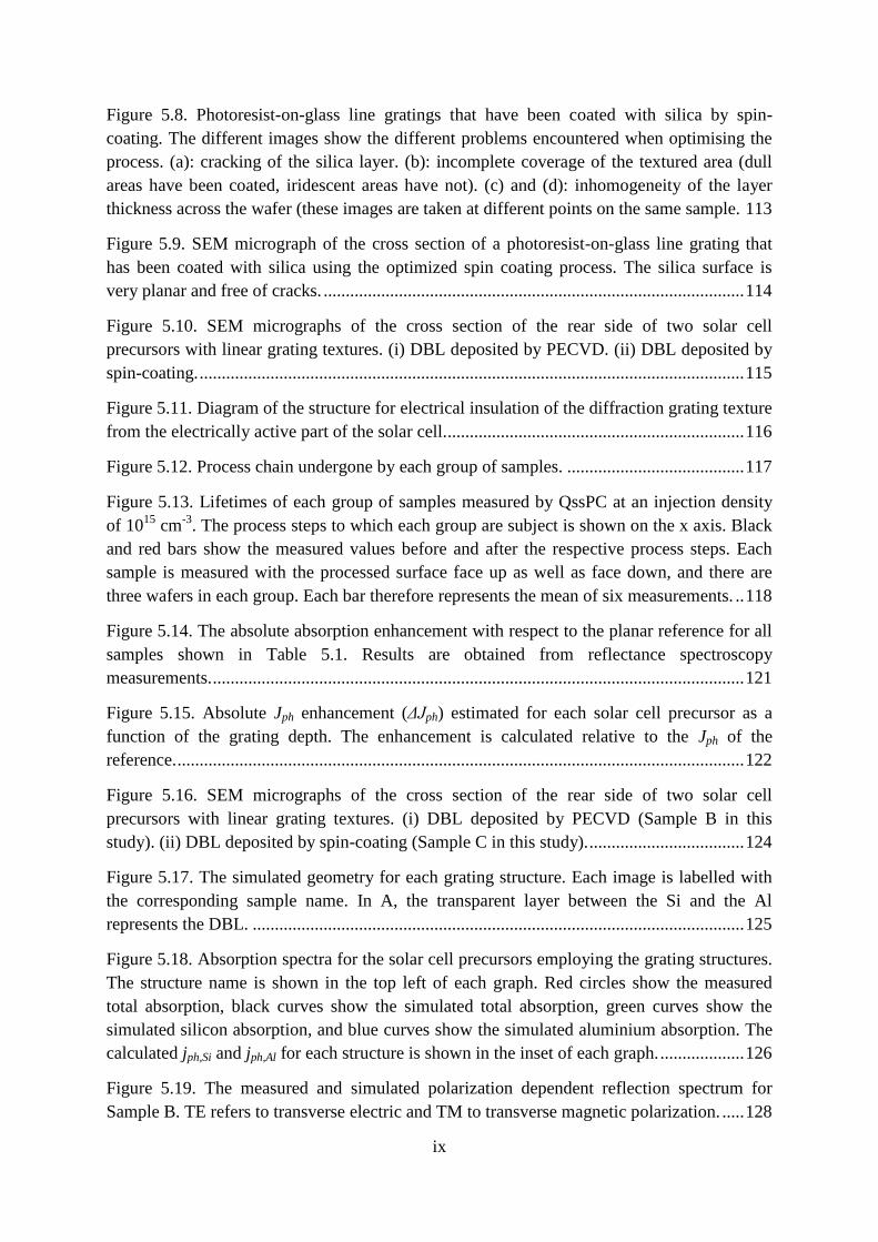


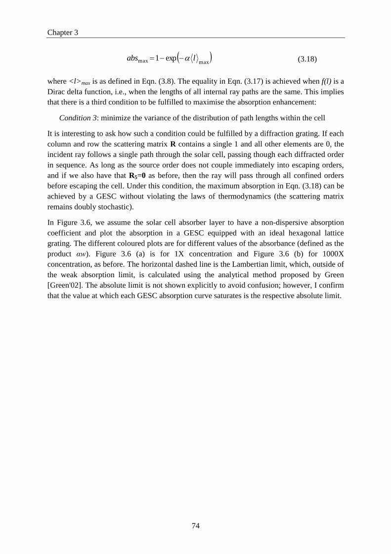


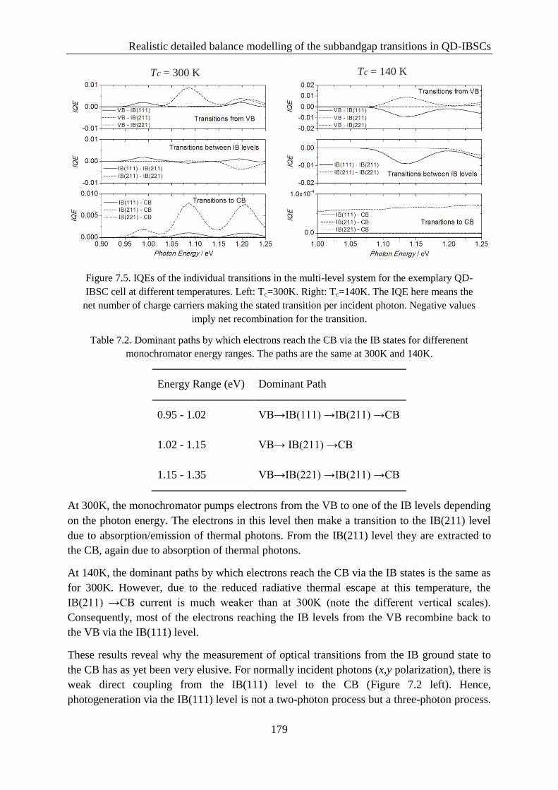


![Manual de usuario CERMA 4 1 - IVE | Instituto Valenciano de la … · 2016-06-09 · 2.2 Uso de la herramienta ... [MANUAL DE USUARIO ] 1 ... La permeabilidad al aire de los huecos](https://static.documents.pub/doc/80x56/5d25d9c488c99326698de5c7/manual-de-usuario-cerma-4-1-ive-instituto-valenciano-de-la-2016-06-09.jpg)


