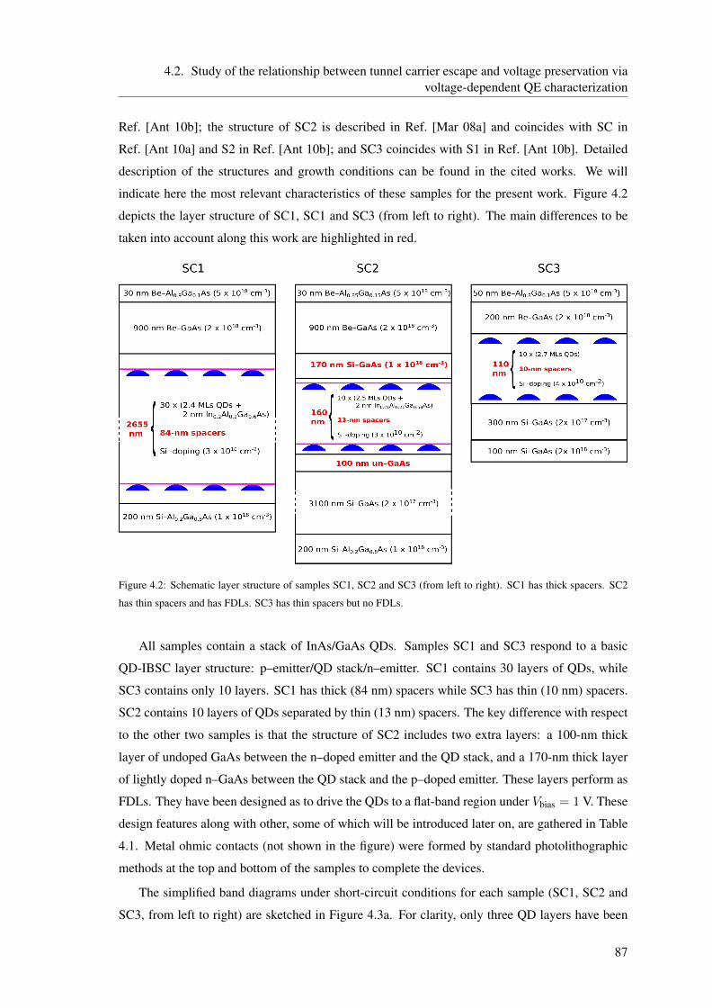
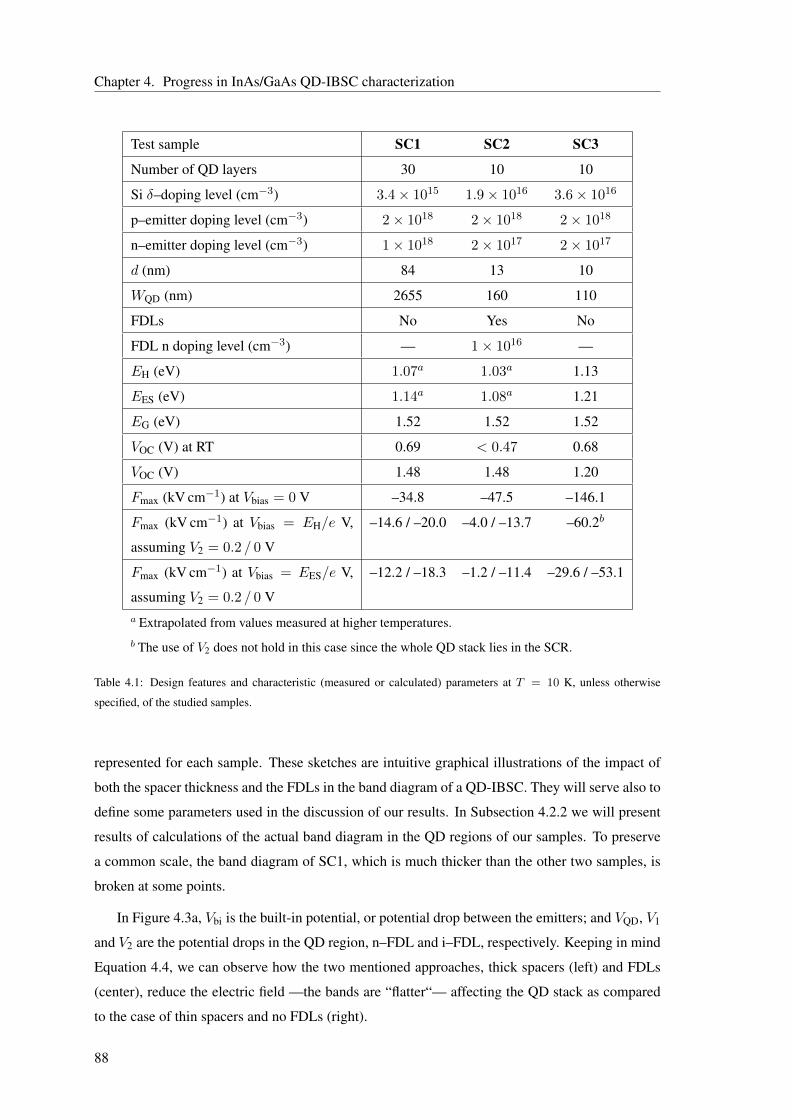
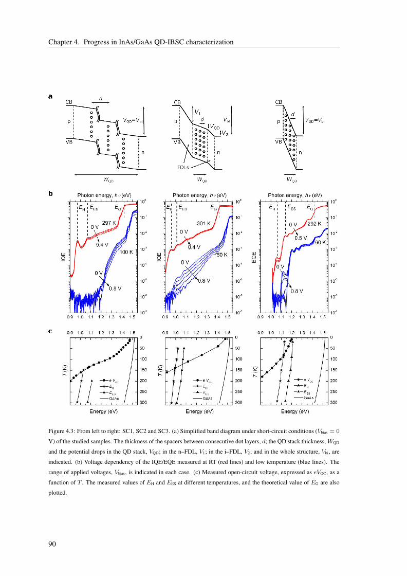
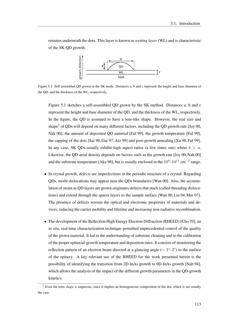
UNIVERSIDAD POLIT ´ ECNICA DE MADRID ESCUELA T ´ ECNICA SUPERIOR DE INGENIEROS DE TELECOMUNICACI ´ ON TESIS DOCTORAL RESEARCH ON WIDE-BANDGAP INTERMEDIATE BAND SOLAR CELLS AND DEVELOPMENT OF EXPERIMENTAL TECHNIQUES FOR THEIR CHARACTERIZATION ´ I˜ nigo Ramiro Gonz´ alez Ingeniero de Telecomunicaci´ on 2015
Transcript
UNIVERSIDAD POLITECNICA DE MADRID
ESCUELA TECNICA SUPERIORDE INGENIEROS DE TELECOMUNICACION
TESIS DOCTORAL
RESEARCH ON WIDE-BANDGAP INTERMEDIATE BANDSOLAR CELLS AND DEVELOPMENT OF EXPERIMENTAL
TECHNIQUES FOR THEIR CHARACTERIZATION
Inigo Ramiro GonzalezIngeniero de Telecomunicacion
2015
UNIVERSIDAD POLITECNICA DE MADRID
Instituto de Energıa SolarDepartamento de Electronica Fısica
Escuela Tecnica Superior de Ingenieros de Telecomunicacion
TESIS DOCTORAL
RESEARCH ON WIDE-BANDGAP INTERMEDIATE BANDSOLAR CELLS AND DEVELOPMENT OF EXPERIMENTAL
TECHNIQUES FOR THEIR CHARACTERIZATION
AUTOR: Inigo Ramiro GonzalezIngeniero de Telecomunicacion
DIRECTORES:Antonio Martı VegaDr. en Ciencias Fısicas
Elisa Antolın FernandezDr. en Ciencias Fısicas
2015
Tribunal nombrado por el Mgfco. y Excmo. Sr. Rector de la Universidad Politecnica de Madrid.
Presidente: Dr. Antonio Luque Lopez
Secretario: Dr. Ignacio Tobıas Galicia
Vocal: Dr. Colin R. Stanley
Vocal: Dr. Turid W. Reenaas
Vocal: Dr. Jose Marıa Ripalda Cobian
Suplente: Dr. German Gonzalez Dıaz
Suplente: Dr. Ignacio Martil de la Plaza
Realizando el acto de defensa y lectura de la Tesis el dıa 8 de mayo de 2015.
En la E.T.S. de Ingenieros de Telecomunicacion.
Calificacion:
EL PRESIDENTE LOS VOCALES
EL SECRETARIO
A mis padres y mi hermano.
He tenido el privilegio de poder llevar a cabo la tesis doctoral en el IES, un lugar cuya ca-
lidad cientıfica y humana rivalizan constantemente por sobresalir. Aquı entre bajo el paraguas
economico de una beca de doctorado de la UPM. Previamente, tuve la oportunidad de estudiar in-
genierıa en una universidad publica de alto nivel y coste accesible a la mayor parte de la poblacion.
Soy plenamente consciente de que, al margen de mi esfuerzo personal, ha sido una sociedad que
apuesta por la educacion publica la que me permite hoy escribir estas lıneas. A esta sociedad se lo
agradezco, y por mantener esta educacion publica peleare.
Los maximos responsables de mi formacion han sido Martı y Elisa. Su impronta cientıfica,
creo, es ya imborrable. Durante estos anos Martı me ha ensanado a respetar la ciencia, la cual,
en justa reciprocidad, ha de tenerle un respeto inmenso. “Primero vamos a descubrir la verdad”
es una frase que encabeza muchas de nuestras discusiones. La pequena intuicion fısica que he
desarrollado se la debo a el. Elisa es la mejor experimentalista que he conocido, y tuvo la genero-
sidad de emplear mucho tiempo en ensenarme todo lo que tanto esfuerzo le llevo descubrir. Espero
haberme empapado de su talento y de su generosidad.
Pablo me ha acompanado literalmente desde el principio, ayudandome y escuchandome siem-
pre de corazon. Es toda una suerte haberle tenido a mi lado dentro y fuera del laboratorio. He
tenido la oportunidad de trabajar con Luque en varias ocasiones. Es difıcil de explicar como de
unos minutos con el se extrae tanta informacion valiosa. Recurriendo al socorrido refranero, dire
que no da puntada sin hilo. Junto a ellos agradezco al resto del grupo de Estudios Fundamentales.
Quiero destacar la inestimable labor y actitud de Irene, siempre dispuesta a ayudar en lo que se
necesita; la alegrıa y la nobleza de Esther; y el companerismo de Juan.
Lo mejor del IES me lo llevo con nombres propios. Rodri, Marta, Manu y Alote me han ayu-
dado y aconsejado especialmente en los ultimos meses de esta tesis. Jorge y Alex han compartido
muchos buenos momentos conmigo. Elisa me ha ayudado enormemente con todos los papeleos de
la tesis durante estos cinco anos, infinitas gracias. Ivan, con quien he compartido menos tiempo
del que me habrıa gustado, es, sencillamente, un tipo estupendo. Y todo el resto: el bondadoso
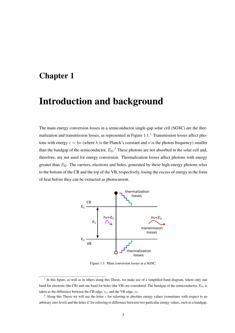
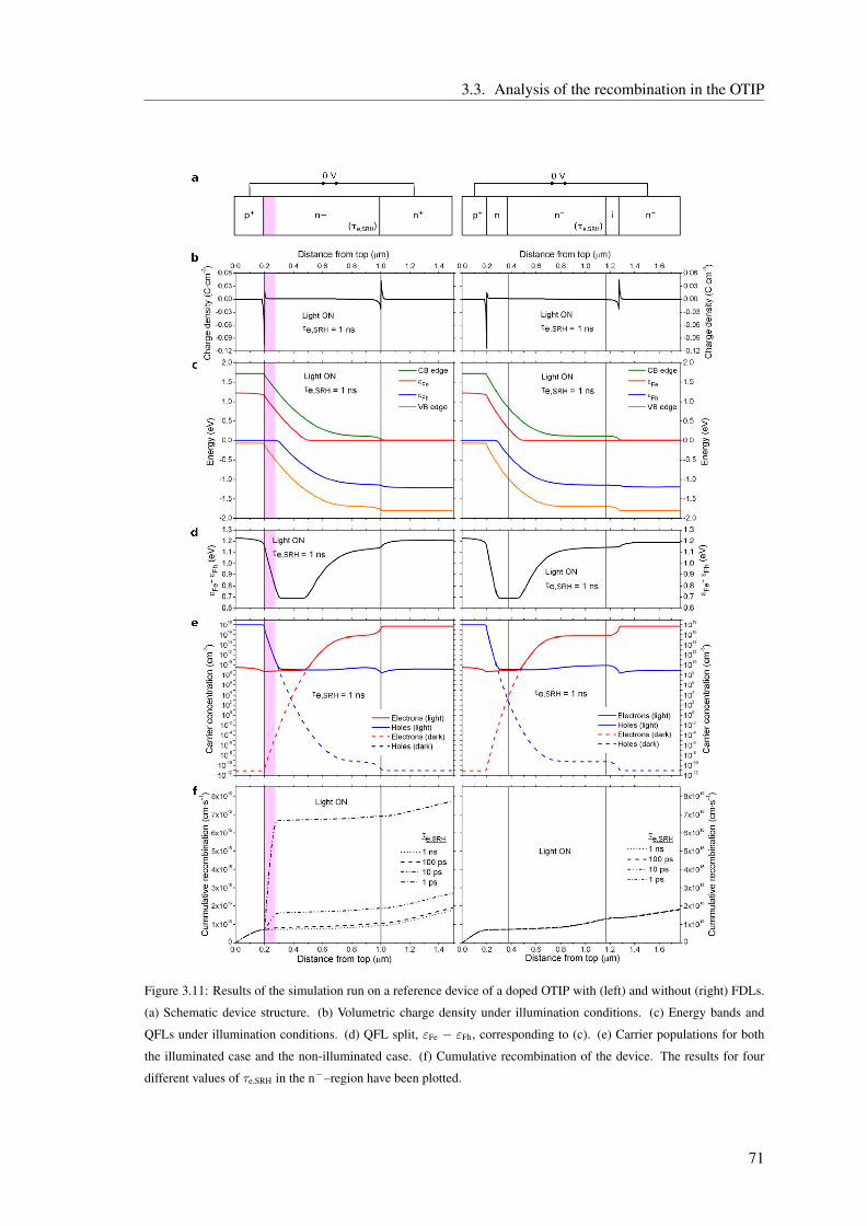
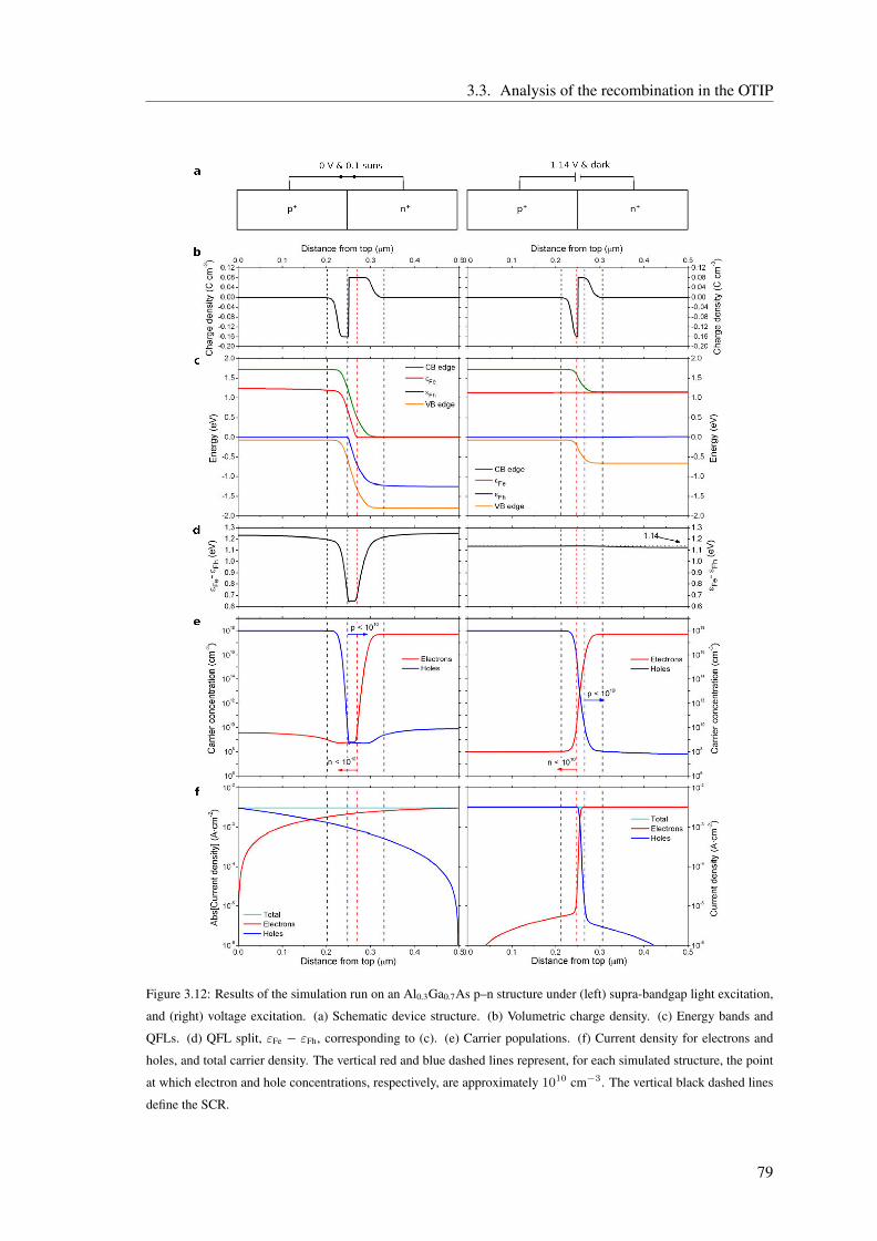
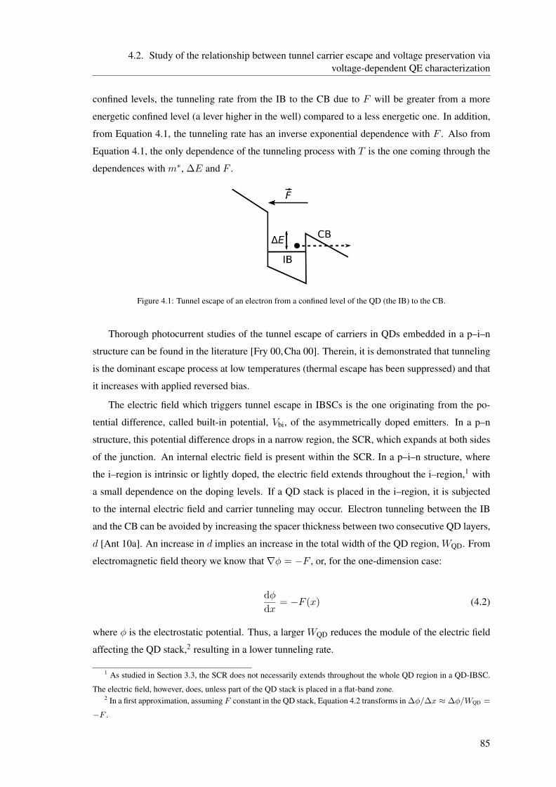
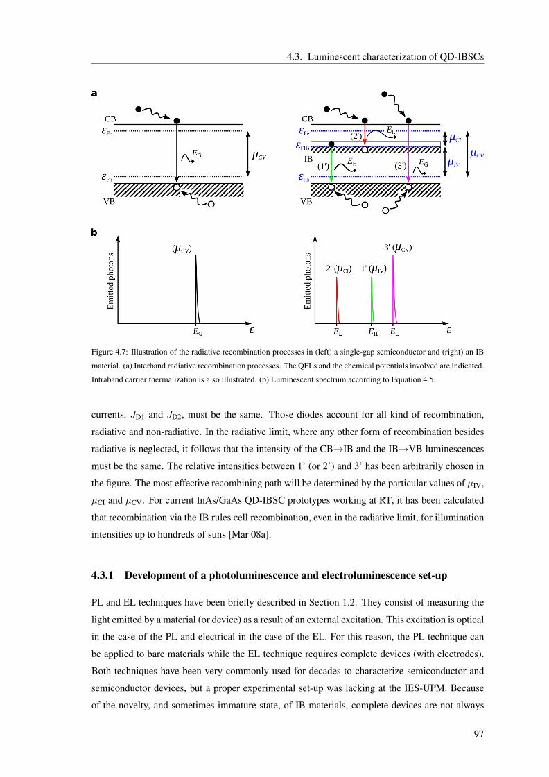
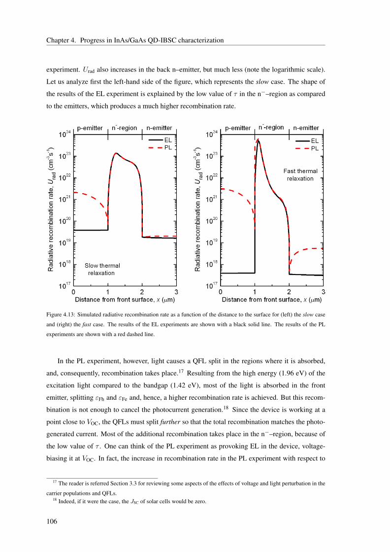
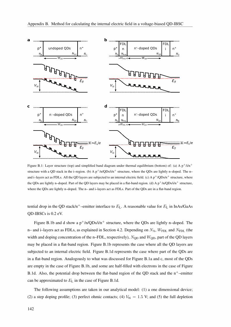
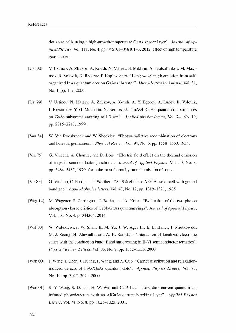
The main energy conversion losses in a semiconductor single-gap solar cell (SGSC) are the ther-
malization and transmission losses, as represented in Figure 1.1.1 Transmission losses affect pho-
tons with energy ε = hν (where h is the Planck’s constant and ν is the photon frequency) smaller
than the bandgap of the semiconductor, EG.2 These photons are not absorbed in the solar cell and,
therefore, are not used for energy conversion. Thermalization losses affect photons with energy
greater than EG. The carriers, electrons and holes, generated by these high-energy photons relax
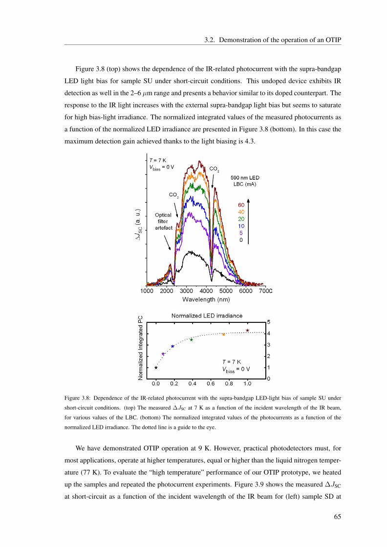
to the bottom of the CB and the top of the VB, respectively, losing the excess of energy in the form
of heat before they can be extracted as photocurrent.
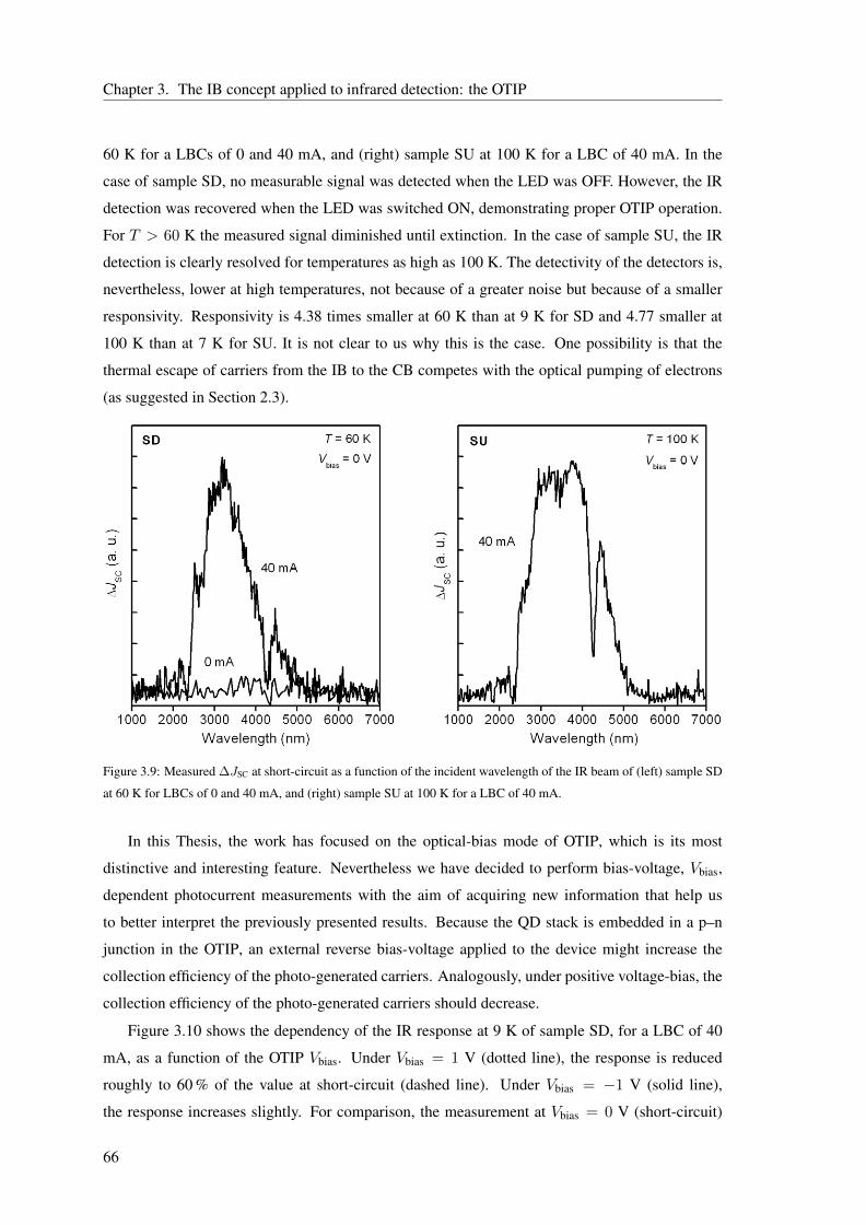
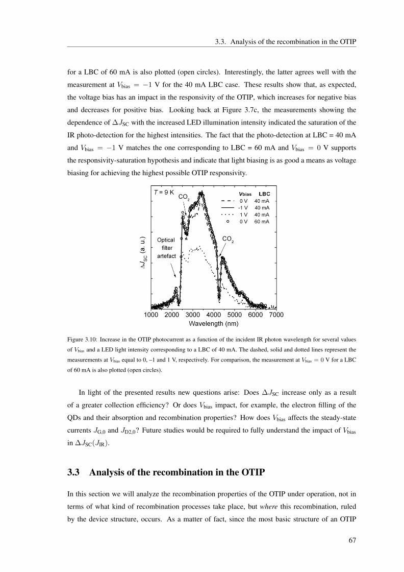
Figure 1.1: Main conversion losses in a SGSC.
1 In this figure, as well as in others along this Thesis, we make use of a simplified band diagram, where only one
band for electrons (the CB) and one band for holes (the VB) are considered. The bandgap of the semiconductor, EG, is
taken as the difference between the CB edge, εC, and the VB edge, εV.2 Along this Thesis we will use the letter ε for referring to absolute energy values (sometimes with respect to an
arbitrary zero level) and the letterE for referring to difference between two particular energy values, such as a bandgap.
1
Chapter 1. Introduction and background
The conversion limiting efficiency of a SGSC is 30.5 %, if no solar concentration3 is used, and
40.7 % for maximum solar concentration [Sho 61, Ara 94]4. This efficiency limit is known as the
Shockley and Queisser (S&Q) limit. In the last years, efficiencies close to the S&Q limit have been
achieved in silicon (25.6 %) and gallium arsenide (28.8 %) devices working at one sun [Gre 14]5.
In order to go beyond the S&Q limit different ideas were proposed. Multi-junction solar cells
(MJSCs) [Jac 55] have been extensively developed in the last decades. They consist of multiple
junctions stacked one above the other in order of decreasing bandgap (from top to bottom), and
connected in series. They are conceived to diminish the thermalization losses by absorbing each
photon in the junction with highest of the possible bandgaps. So far, devices with efficiencies
as high as 44.4 ,6 under illumination equivalent to 302 suns, have been fabricated [Gre 14]. The
branch of photovoltaic energy that studies and produces devices for operation under concentrated
light is known as concentrating photovoltaics (CPV).
In a less mature state we find the so-called novel concepts in photovoltaics, which lay out new
ways of exceeding the S&Q limit. Among them we can underline three: the intermediate band
solar cell (IBSC) [Luq 97], the multiple-exciton-generation solar cell (MEGSC) [Noz 02] and the
hot-carrier solar cell (HCSC) [Ros 82, Wur 97]. The MEGSC and the HCSC are at a very early
stage of experimental reasearch (see Ref. [Ram 13] for a review). These two concepts aim to
minimize the thermalization losses and have a limiting efficiency of 85 % under maximum solar
concentration. On the other hand, the IBSC aims to reduce the transmission losses of the solar cell
and has a limiting efficiency of 63.2 % under maximum solar concentration. The IBSC concept is
at an advanced point of the research, experimental as well as theoretical. This introductory chapter
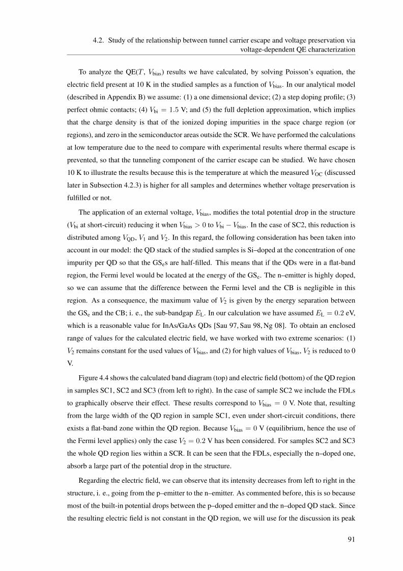
is devoted to explain the basis of the IBSC as well as the main bottlenecks in IBSC development.
We will also review the experimental state of the art of this novel concept, which will be essential
for apprehending and contextualizing the work presented in this Thesis.
3 The term solar-light concentration, or simply solar concentration, refers to the management of light so that a solar
cell receives more solar energy than it would if it was barely exposed to the sun. Typically this is achieved using lenses
or mirrors. If the solar cell is barely exposed to the sun it is said to be under one-sun illumination, or at one sun; if
it receives twice the energy – with the same spectral distribution – it is said to be at two suns, and so on. Attending
exclusively to geometrical factors (size of the sun and sun–Earth distance) the maximum concentration achievable is
46050 suns – for a solar cell surrounded by a medium with refraction index equal to one.4 These efficiency limits are calculated for a cell temperature of 300 K and assuming that the sun emits light as a
black body at 6000 K.5 Efficiencies measured under the ASTM G-173-03 global beam AM1.5 spectrum at a cell temperature of 25 °C.6 Efficiency measured under the ASTM G-173-03 direct beam AM1.5 spectrum at a cell temperature of 25 °C.
2
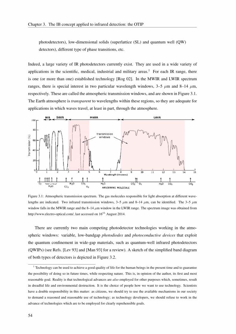
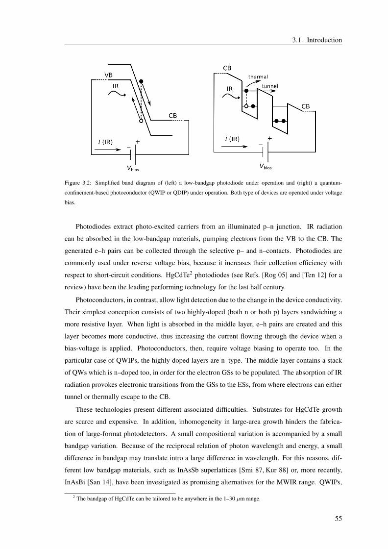
1.1. Introduction to the IBSC
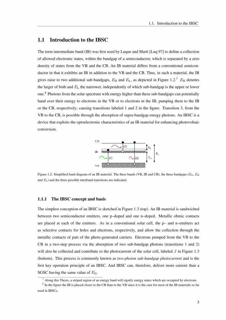
1.1 Introduction to the IBSC
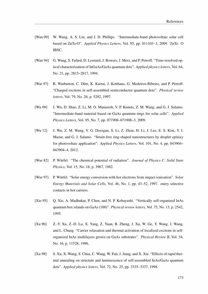
The term intermediate band (IB) was first used by Luque and Martı [Luq 97] to define a collection
of allowed electronic states, within the bandgap of a semiconductor, which is separated by a zero
density of states from the VB and the CB. An IB material differs from a conventional semicon-
ductor in that it exhibits an IB in addition to the VB and the CB. Thus, in such a material, the IB
gives raise to two additional sub-bandgaps, EH and EL, as depicted in Figure 1.2.7 EH denotes
the larger of both and EL the narrower, independently of which sub-bandgap is the upper or lower
one.8 Photons from the solar spectrum with energy higher than these sub-bandgaps can potentially
hand over their energy to electrons in the VB or to electrons in the IB, pumping them to the IB
or the CB, respectively; causing transitions labeled 1 and 2 in the figure. Transition 3, from the
VB to the CB, is possible through the absorption of supra-bandgap energy photons. An IBSC is a
device that exploits the optoelectronic characteristics of an IB material for enhancing photovoltaic
conversion.
Figure 1.2: Simplified band diagram of an IB material. The three bands (VB, IB and CB), the three bandgaps (EG, EH
and EL) and the three possible interband transitions are indicated.
1.1.1 The IBSC concept and basis
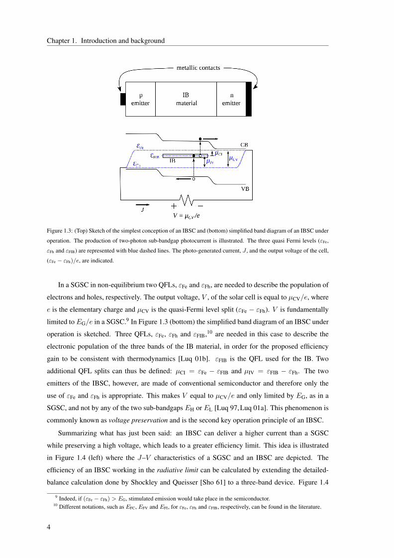
The simplest conception of an IBSC is sketched in Figure 1.3 (top). An IB material is sandwiched
between two semiconductor emitters, one p–doped and one n–doped. Metallic ohmic contacts
are placed at each of the emitters. As in a conventional solar cell, the p– and n–emitters act
as selective contacts for holes and electrons, respectively, and allow the collection through the
metallic contacts of part of the photo-generated carriers. Electrons pumped from the VB to the
CB in a two-step process via the absorption of two sub-bandgap photons (transitions 1 and 2)
will also be collected and contribute to the photocurrent of the solar cell, labeled J in Figure 1.3
(bottom). This process is commonly known as two-photon sub-bandgap photocurrent and is the
first key operation principle of an IBSC. And IBSC can, therefore, deliver more current than a
SGSC having the same value of EG.7 Along this Thesis, a striped region of an energy band will signify energy states which are occupied by electrons.8 In the figure the IB is placed closer to the CB than to the VB since it is the case for most of the IB materials so far
used in IBSCs.
3
Chapter 1. Introduction and background
Figure 1.3: (Top) Sketch of the simplest conception of an IBSC and (bottom) simplified band diagram of an IBSC under
operation. The production of two-photon sub-bandgap photocurrent is illustrated. The three quasi Fermi levels (εFe,
εFh and εFIB) are represented with blue dashed lines. The photo-generated current, J , and the output voltage of the cell,
(εFe − εFh)/e, are indicated.
In a SGSC in non-equilibrium two QFLs, εFe and εFh, are needed to describe the population of
electrons and holes, respectively. The output voltage, V , of the solar cell is equal to µCV/e, where
e is the elementary charge and µCV is the quasi-Fermi level split (εFe − εFh). V is fundamentally
limited to EG/e in a SGSC.9 In Figure 1.3 (bottom) the simplified band diagram of an IBSC under
operation is sketched. Three QFLs, εFe, εFh and εFIB,10 are needed in this case to describe the
electronic population of the three bands of the IB material, in order for the proposed efficiency
gain to be consistent with thermodynamics [Luq 01b]. εFIB is the QFL used for the IB. Two
additional QFL splits can thus be defined: µCI = εFe − εFIB and µIV = εFIB − εFh. The two
emitters of the IBSC, however, are made of conventional semiconductor and therefore only the
use of εFe and εFh is appropriate. This makes V equal to µCV/e and only limited by EG, as in a
SGSC, and not by any of the two sub-bandgaps EH or EL [Luq 97,Luq 01a]. This phenomenon is
commonly known as voltage preservation and is the second key operation principle of an IBSC.
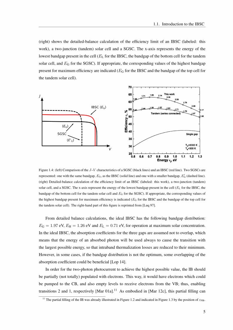
Summarizing what has just been said: an IBSC can deliver a higher current than a SGSC
while preserving a high voltage, which leads to a greater efficiency limit. This idea is illustrated
in Figure 1.4 (left) where the J–V characteristics of a SGSC and an IBSC are depicted. The
efficiency of an IBSC working in the radiative limit can be calculated by extending the detailed-
balance calculation done by Shockley and Queisser [Sho 61] to a three-band device. Figure 1.4
9 Indeed, if (εFe − εFh) > EG, stimulated emission would take place in the semiconductor.10 Different notations, such as EFC, EFV and EFI, for εFe, εFh and εFIB, respectively, can be found in the literature.
4
1.1. Introduction to the IBSC
(right) shows the detailed-balance calculation of the efficiency limit of an IBSC (labeled: this
work), a two-junction (tandem) solar cell and a SGSC. The x-axis represents the energy of the
lowest bandgap present in the cell (EL for the IBSC, the bandgap of the bottom cell for the tandem
solar cell, and EG for the SGSC). If appropriate, the corresponding values of the highest bandgap
present for maximum efficiency are indicated (EG for the IBSC and the bandgap of the top cell for
the tandem solar cell).
Figure 1.4: (left) Comparison of the J–V characteristics of a SGSC (black lines) and an IBSC (red line). Two SGSCs are
represented: one with the same bandgap,EG, as the IBSC (solid line) and one with a smaller bandgap,E′G (dashed line).
(right) Detailed-balance calculation of the efficiency limit of an IBSC (labeled: this work), a two-junction (tandem)
solar cell, and a SGSC. The x-axis represent the energy of the lowest bandgap present in the cell (EL for the IBSC, the
bandgap of the bottom cell for the tandem solar cell and EG for the SGSC). If appropriate, the corresponding values of
the highest bandgap present for maximum efficiency is indicated (EG for the IBSC and the bandgap of the top cell for
the tandem solar cell). The right-hand part of this figure is reprinted from [Luq 97].
From detailed balance calculations, the ideal IBSC has the following bandgap distribution:
EG = 1.97 eV, EH = 1.26 eV and EL = 0.71 eV, for operation at maximum solar concentration.
In the ideal IBSC, the absorption coefficients for the three gaps are assumed not to overlap, which
means that the energy of an absorbed photon will be used always to cause the transition with
the largest possible energy, so that intraband thermalization losses are reduced to their minimum.
However, in some cases, if the bandgap distribution is not the optimum, some overlapping of the
absorption coefficient could be beneficial [Lop 14].
In order for the two-photon photocurrent to achieve the highest possible value, the IB should
be partially (not totally) populated with electrons. This way, it would have electrons which could
be pumped to the CB, and also empty levels to receive electrons from the VB; thus, enabling
transitions 2 and 1, respectively [Mar 01a].11 As embodied in [Mar 12c], this partial filling can
11 The partial filling of the IB was already illustrated in Figure 1.2 and indicated in Figure 1.3 by the position of εFIB.
5
Chapter 1. Introduction and background
be achieved in different manners: (1) naturally, if the IB material exhibits a metallic band; (2) if
the IB material naturally presents a filled or empty band, compensation doping is necessary to,
respectively, either depopulate or populate part of the IB states; (3) for an intrinsic IB material in
which the IB states are naturally empty, it has been calculated that, under high solar concentra-
tion, the photo-filling of these states can sustain a useful population of electrons that allows high
efficiencies to be achieved [Str 09, Luq 10b]; (4) regardless of the a priori population of the IB
and the intended doping, it has been discussed how, if the IB material lies on the depletion re-
gion of the solar cell, the effective population of the IB states is ruled by their location inside this
region [Mar 08a].
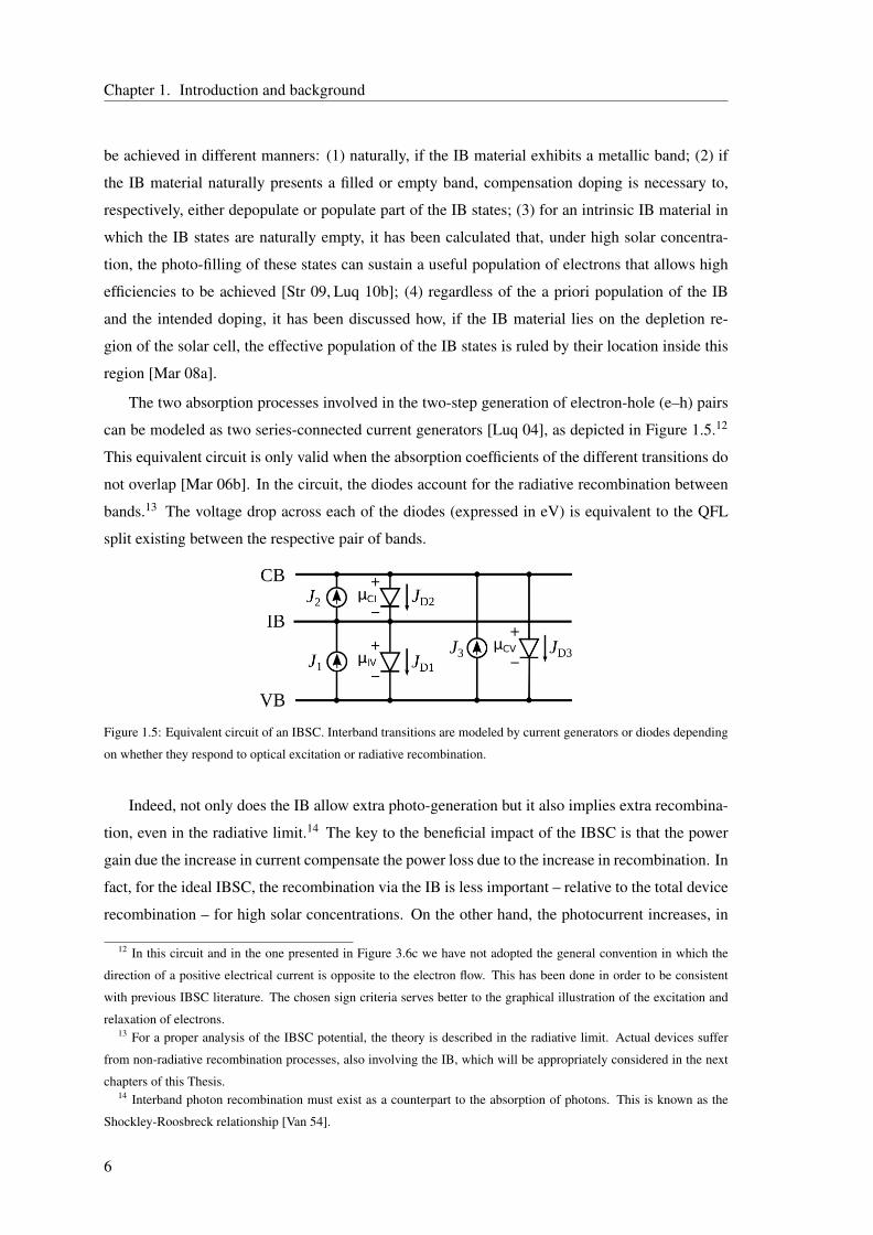
The two absorption processes involved in the two-step generation of electron-hole (e–h) pairs
can be modeled as two series-connected current generators [Luq 04], as depicted in Figure 1.5.12
This equivalent circuit is only valid when the absorption coefficients of the different transitions do
not overlap [Mar 06b]. In the circuit, the diodes account for the radiative recombination between
bands.13 The voltage drop across each of the diodes (expressed in eV) is equivalent to the QFL
split existing between the respective pair of bands.
Figure 1.5: Equivalent circuit of an IBSC. Interband transitions are modeled by current generators or diodes depending
on whether they respond to optical excitation or radiative recombination.
Indeed, not only does the IB allow extra photo-generation but it also implies extra recombina-
tion, even in the radiative limit.14 The key to the beneficial impact of the IBSC is that the power
gain due the increase in current compensate the power loss due to the increase in recombination. In
fact, for the ideal IBSC, the recombination via the IB is less important – relative to the total device
recombination – for high solar concentrations. On the other hand, the photocurrent increases, in
12 In this circuit and in the one presented in Figure 3.6c we have not adopted the general convention in which the
direction of a positive electrical current is opposite to the electron flow. This has been done in order to be consistent
with previous IBSC literature. The chosen sign criteria serves better to the graphical illustration of the excitation and
relaxation of electrons.13 For a proper analysis of the IBSC potential, the theory is described in the radiative limit. Actual devices suffer
from non-radiative recombination processes, also involving the IB, which will be appropriately considered in the next
chapters of this Thesis.14 Interband photon recombination must exist as a counterpart to the absorption of photons. This is known as the
Shockley-Roosbreck relationship [Van 54].
6
1.1. Introduction to the IBSC
first approximation, linearly with the concentration. Consequently, the potential benefits of the IB
are greater for high solar concentration.
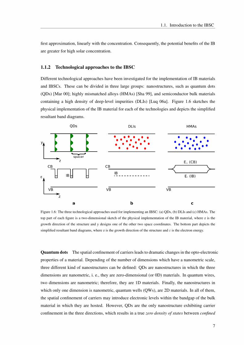
1.1.2 Technological approaches to the IBSC
Different technological approaches have been investigated for the implementation of IB materials
and IBSCs. These can be divided in three large groups: nanostructures, such as quantum dots
containing a high density of deep-level impurities (DLIs) [Luq 06a]. Figure 1.6 sketches the
physical implementation of the IB material for each of the technologies and depicts the simplified
resultant band diagrams.
Figure 1.6: The three technological approaches used for implementing an IBSC: (a) QDs, (b) DLIs and (c) HMAs. The
top part of each figure is a two-dimensional sketch of the physical implementation of the IB material, where z is the
growth direction of the structure and y designs one of the other two space coordinates. The bottom part depicts the
simplified resultant band diagrams, where z is the growth direction of the structure and ε is the electron energy.
Quantum dots The spatial confinement of carriers leads to dramatic changes in the opto-electronic
properties of a material. Depending of the number of dimensions which have a nanometric scale,
three different kind of nanostructures can be defined: QDs are nanostructures in which the three
dimensions are nanometric, i. e., they are zero-dimensional (or 0D) materials. In quantum wires,
two dimensions are nanometric; therefore, they are 1D materials. Finally, the nanostructures in
which only one dimension is nanometric, quantum wells (QWs), are 2D materials. In all of them,
the spatial confinement of carriers may introduce electronic levels within the bandgap of the bulk
material in which they are hosted. However, QDs are the only nanostructure exhibiting carrier
confinement in the three directions, which results in a true zero density of states between confined
7
Chapter 1. Introduction and background
states15 in their potential well. This unique feature is, in principle, essential for the achievement of
actual IBSCs since a high enough density of states between the IB and the CB (or the VB) would
facilitate thermal electronic exchange between those two bands. In order for an IBSC to exceed
the efficiency limit of SGSCs, thermal coupling between the bands must be minimized [Luq 01b].
The QD-IBSC relies on the confined levels of the QDs to form the IB. The position of the
IB depends on the materials combination and the size and shape of the QDs and therefore can be
tuned – to some extent – to fit the requirements of the IBSC. QD technology is, in some cases,
very mature, since it has been widely investigated in many branches of the electronics field. For
this reason, the first and the majority of the IBSC prototypes fabricated to date have used this
technology.
Deep-level impurities Deep levels in semiconductors are well known to act as non-radiative re-
combination (NRR) centers, degrading the electro-optical properties of semiconductors. However,
as described by Luque et al. [Luq 06a], if the concentration of impurities exceeds a certain limit
(known as the Luque-Mott limit [Mot 68, Luq 06a]), the wavefunctions of the electrons in the
deep levels will delocalize, forming a band and minimizing NRR. This band acts as the IB in a
DLI-based IBSC.
Highly mismatched alloys HMAs are a recently discovered class of semiconductor compounds
in which the introduction of highly electronegative atoms leads to unusual changes in the CB of
the alloy. This phenomenon is explained by the band anticrossing model [Sha 99, Wal 00], which
describes the split of the CB of the alloy when those atoms are introduced. As a result, two
distinct bands emerge: E− and E+, for the least and the most energetic, respectively. Using IB
nomenclature, E− would act as the IB and E+ as the CB.
In this Thesis, when referring to a QD system, we will use the notation X/Y, where X is the QD
material and Y is the material of the host matrix. When referring to HMAs we will use the notation
X:Y where X is the main alloy and Y is the element introduced in small quantities, responsible for
the band anticrossing effect. When referring to a bulk material with DLIs, we will use the notation
X:Y, where X is the bulk material and Y is the DLI. An element will be placed in parentheses to
indicate that it is sometimes, but not always, part of the studied material.
So far, the most used fabrication method for QD and HMA approaches is the molecular beam
epitaxy (MBE). This growth technique will be introduced in Chapter 5. The metalorganic vapour
phase epitaxy (MOVPE)16 method has also been used for fabricating QD-IBSCs. In contrast
to MBE, the growth of crystals by MOVPE is done by chemical reactions and not by physical
15 In contrast to the electronic levels of the bands of a bulk semiconductor, which are extended.16 Also known as metalorganic chemical vapour deposition (MOCVD).
8
1.1. Introduction to the IBSC
deposition. In addition to MBE, other techniques, such as ion implantation, have also been used
for the bulk material with DLIs approach.
1.1.3 Main shortcomings of practical QD-IBSCs
As it will be reviewed in Section 1.2, QD-IBSC prototypes served to demonstrate the two operation
principles of the IBSC. However, they also revealed some crucial problems of real devices that
have made impossible, so far, the achievement of a high-efficiency IBSC. Two main problems
restrict the performance of state-of-the-art QD-IBSCs. The first one has to do with inefficient
sub-bandgap absorption and, the second one, with an excessive voltage degradation of the IBSC
with respect to its reference cell.17 In general terms, these problems have affected almost all IBSC
prototypes, irrespective their technology. We will focus here on QD-IBSCs for describing them,
for two reasons: firstly, both issues have been discovered and studied first and more extensively
in InAs/GaAs QD-IBSCs, and secondly, the research work presented in this Thesis focuses on
QD-IBSCs, so it is essential to understand their specificities.
Absorption in the QD stack of IBSCs is weak in both the VB→IB and the IB→CB transitions.
The main reason for this is the combination of a low volumetric density of QDs (in the 1015–
1016 cm−3 range) and a limited number QD layers in the QD stack (typically less than 50). The
QD volumetric density can be increased by increasing the QD areal density (for example, using
substrates with higher crystallographic indices [Aka 98,Aka 02]) and/or by reducing the thickness
of the spacers (see Figure 1.6) between QD layers. The latter alternative will be analyzed in
Section 4.2. Accumulated strain in the QD stack is responsible for the limitation of the number
of QD-layers than can be grown with good opto-electronic properties. To address this problem
and improve the material quality, a small amount of N [Osh 08], P [Pop 08, Alo 10, Lag 07a] or
Sb [Liu 12b] has been included, in some cases, in the host material. Also, recently, cells with up to
150 InGaAs/GaAs QD layers and QD stacks containing up to 400 layers have been manufactured
without using strain-compensation techniques [Sug 12].
Some experimental work has been carried out on measuring the absorption strength of the
VB→IB transition [War 97, Fry 00]. The IB→CB transition has been widely characterized in the
framework of quantum-dot infrared photodetectors (QDIPs),18 but a proper study of the IB→CB
absorptivity has been left in the background, because the figure of merit of these devices is a
complex combination of QD absorptivity, carrier collection and dark current. Recently, theoretical
work has allowed the understanding of the nature of the sub-bandgap absorption in QD-IBSCs
17 As it is common practice in the literature, throughout this Thesis, for a given IBSC, the term reference cell will
refer to a solar cell consisting of the same semiconductor structure as the corresponding IBSC, but in which the IB
material has been replaced by a conventional (single-gap) semiconductor.18 Refer to Chapter 3 for a description of the QDIP operation and for QDIP references.
9
Chapter 1. Introduction and background
[Luq 13b, Luq 13a, Luq 13d]. As a result, it has been calculated that a reduction in the QD size
would increase absorption in the VB→IB and the IB→CB transitions [Mel 12, Mel 13]. Note that
smaller-size QDs are compatible with an increase in the QD areal density.
The vast majority of the QDs used in QD-IBSCs are type-I QDs19 grown by the Stranski-
Krastanov (SK) mode. Some basic concepts and characteristics of SK growth mode will be de-
scribed in Section 5.1. Two important features for the following discussion are:
• After the formation of the dots, a very thin (∼ 0.5–3 nm) layer of QD material, the wet-
ting layer (WL), remains underneath the QD layer. The WL introduces a bandgap in the
structure, EWL, which is somewhere in between that of the QDs and EG.
• In QD growth, defects appear near the QD boundaries due to the lattice mismatch. Also,
the strain inherent to the SK growth mode may originate defects and dislocations in the
subsequently-grown crystal.
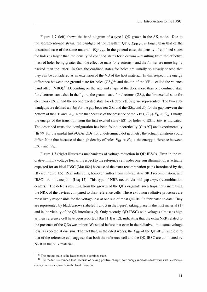
Figure 1.7: (left) Band diagram of a type-I QD grown by the SK mode. The different relevant energy gaps (EG,
EWL, EQD,uns, EQD,str, EES, EH and EL), three confined states for electrons (GSe, ES1e and ES2e), and the VBO are
indicated. (right) Source mechanisms of voltage reduction in QD-IBSCs. Black arrows represent non-radiative SRH
recombination processes: (1) in the host material and (5) in the vicinity of the QD interfaces. Red arrows represent
thermal processes: (2) relaxation of carriers and (3) thermal carrier escape. The dashed arrow, labeled (4), represents
tunnel carrier escape.
19 QDs can be classified according to the resulting band diagram of the structure. Type-I QDs present charge con-
finement for both types of carriers, electrons and holes (see Figure 1.7). Conversely, in type-II QDs only one type of
carrier, electrons or holes, is confined.
10
1.1. Introduction to the IBSC
Figure 1.7 (left) shows the band diagram of a type-I QD grown in the SK mode. Due to
the aforementioned strain, the bandgap of the resultant QDs, EQD,str, is larger than that of the
unstrained case of the same material, EQD,uns. In the general case, the density of confined states
for holes is larger than the density of confined states for electrons – resulting from the effective
mass of holes being greater than the effective mass for electrons – and the former are more highly
packed than the latter. In fact, the confined states for holes are usually so closely spaced that
they can be considered as an extension of the VB of the host material. In this respect, the energy
difference between the ground state for holes (GSh)20 and the top of the VB is called the valence
band offset (VBO).21 Depending on the size and shape of the dots, more than one confined state
for electrons can exist. In the figure, the ground state for electrons (GSe), the first excited state for
electrons (ES1e) and the second excited state for electrons (ES2e) are represented. The two sub-
bandgaps are defined as: EH for the gap between GSe and the GSh, andEL for the gap between the
bottom of the CB and GSe. Note that because of the presence of the VBO,EH +EL < EG. Finally,
the energy of the transition from the first excited state (ES) for holes to ES1e, EES is indicated.
The described transition configuration has been found theoretically [Cus 97] and experimentally
[Its 99] for pyramidal InAs/GaAs QDs; for undetermined dot geometry the actual transitions could
differ. Note that because of the high density of holes EES ≈ EH + the energy difference between
ES1e and GSe.
Figure 1.7 (right) illustrates mechanisms of voltage reduction in QD-IBSCs. Even in the ra-
diative limit, a voltage loss with respect to the reference cell under one-sun illumination is actually
expected for an ideal IBSC [Mar 08a] because of the extra recombination paths introduced by the
IB (see Figure 1.5). Real solar cells, however, suffer from non-radiative SRH recombination, and
IBSCs are no exception [Luq 12]. This type of NRR occurs via mid-gap traps (recombination
centers). The defects resulting from the growth of the QDs originate such traps, thus increasing
the NRR of the devices compared to their reference cells. These extra non-radiative processes are
most likely responsible for the voltage loss at one sun of most QD-IBSCs fabricated to date. They
are represented by black arrows (labeled 1 and 5 in the figure), taking place in the host material (1)
and in the vicinity of the QD interfaces (5). Only recently, QD-IBSCs with voltages almost as high
as their reference cell have been reported [Bai 11,Bai 12], indicating that the extra NRR related to
the presence of the QDs was minor. We stated before that even in the radiative limit, some voltage
loss is expected at one sun. The fact that, in the cited works, the VOC of the QD-IBSC is close to
that of the reference cell suggests that both the reference cell and the QD-IBSC are dominated by
NRR in the bulk material.
20 The ground state is the least energetic confined state.21 The reader is reminded that, because of having positive charge, hole energy increases downwards while electron
energy increases upwards in the band diagrams.
11
Chapter 1. Introduction and background
As it was pointed out in Subsection 1.1.1, under high solar concentration the IBSC should
present negligible voltage loss with respect to the reference cell. However, experiments under
concentrated light have revealed that this is not the case. In fact, the open-circuit voltage, VOC, of
QD-IBSCs at RT does not exceedEH/e [Lin 11a,Lin 13b]. It has been demonstrated [Ant 10b] that
thermal carrier escape22 prevents the QFL split between the IB and the CB. Thermal processes
are depicted by red arrows in Figure 1.7 (right). Arrows labeled (2) represent carrier thermal
relaxation while arrow (3) represents thermal carrier escape. Studies at low temperature (LT) have
shown that tunnel carrier escape23 may also take place in QD-IBSCs [Ant 10a], with identical
detrimental effects in the VOC. Tunnel carrier escape is represented by the arrow labeled (4) in
Figure 1.7.24 Both escape mechanisms impose a fundamental limitation to the VOC of QD-IBSCs.
It should be noted that the previous discussion has focused on type-I SK QDs. Other type
of QDs may present significant theoretical and practical differences. For example, it has been
suggested that some type-II SK QDs are good candidates for implementing IBSCs, since they
exhibit a band alignment with no VBO and may present greater sub-bandgap absorption [Luq 13c].
Also, QDs whose growth is not based on difference in lattice constant but on difference in crystal
structure have been proposed as promising IB candidate materials [Ant 11]. These QDs are grown
strain-free and can be of a very small size, which reduces the number undesirable ESs25 but shifts
the IB towards higher energies.
1.2 State of the art of experimental IBSCs
In this Section, we will present a record of the experimental achievements in IBSCs obtained up
to December 2014. A first distinction can be made among the variety of experimental evidences
of IB-related phenomena: those obtained on complete IBSC—at device level—and those obtained
on bare IB materials—at material level. The two operation principles of an IBSC can only be ver-
ified through characterization of IBSCs at device level, and not at material level. However, when
characterizing at device level it is difficult to isolate the impact of a single IB-related phenomenon
because of the many other parameters that play a role in the operation of a solar cell. Hence, it is
useful to perform characterization at material level as a help to understand the device behavior.
22 Thermal carrier escape will be reviewed and investigated in Section 2.2.23 Tunnel carrier escape will be reviewed and investigated in Section 4.2.24 As it will be studied in Section 4.2, tunnel escape depends on the electric filed. In Figure 1.7 (right), for the sake
of simplicity, the energy bands are flat, which corresponds with the absence of electric field. Were this the case of an
actual band diagram, tunnel escape would be minimal.25 The inexpediency for IBSC purposes of the ESs will be argued in Chapters 2 and 4.
12
1.2. State of the art of experimental IBSCs
1.2.1 Characterization techniques
Along this Thesis different IBSC characterization results will be discussed. Hence, it is important
to briefly present them, emphasizing their ability to asses IB-related behavior. Some of the tech-
niques employed for IBSC characterization have been traditionally used in photovoltaics.26 Others
have been expressly developed for characterizing IBSCs [Ant 08, Lin 13b]. We describe here the
experimental techniques most commonly employed. Eight techniques will be described. Tech-
niques 1–5 are applied to IBSCs while techniques 6–8 are applied to IB materials. As a graphic
example, one representative experimental result is included for each characterization technique.
1.2.1.1 Sub-bandgap spectral response or quantum efficiency
The production of photocurrent, expressed as spectral response (SR) or quantum efficiency (QE),
is probably the most reported result in IBSC characterization. This technique consists of resolving
spectrally the photocurrent produced in the solar cell when illuminated under short-circuit condi-
tions. A SGSC cannot exploit photons with energy lower, or wavelength higher, than that of the
bandgap to produce current. The production of current due to sub-bandgap illumination in an IBSC
gives, therefore, a strong evidence of the presence of intermediate states within the semiconductor
bandgap.
In SGSC characterization, it is not unusual to add white-light bias so that the QE be measured
under conditions similar to one sun illumination. In the case of an IBSC, the two ways of mea-
suring the QE, with or without light bias, may provide qualitatively different results because of
the multi-photon processes that are expected if broadband illumination is present. To date this ex-
periment has been generally performed without light bias when characterizing IBSCs, which must
be taken into account when interpreting the results. An ideal IBSC should not generate photocur-
rent when illuminated only with monochromatic sub-bandgap light. However, three mechanisms
can make it possible. Firstly, if the absorption coefficients for transitions 1 and 2 in Figure 1.2
overlap, a monochromatic beam of photons with energy higher than EH could produce both tran-
sitions [Luq 01a,Cua 04]. Secondly, even if only one of these two transitions is optically activated,
impact ionization processes could lead to the accomplishment of the other, as an alternative to
the missing optical transition [Luq 03]. Thirdly, tunnel and thermal carrier escape could accom-
plish the missing transition, as described in Subsection 1.1.3. A device exhibiting any of these
mechanisms is expected to have a lower potential efficiency than an IBSC with proper two-photon
absorption.
26 Special care must be taken when analyzing and interpreting experimental results obtained by the conventional tech-
niques used to characterize photovoltaic devices. A comprehensive guide to the understanding of the characterization
of IBSCs can be found in [Mar 12b].
13
Chapter 1. Introduction and background
Figure 1.8 shows the monochromatic spectral response of an InAs/GaAs QD-IBSC at LT, mea-
sured by Martı et al [Mar 06a]. Contribution of sub-bandgap energy photons is clearly visible in
the response of the IBSC sample (curve 1). The low energy edge of the sub-bandgap photocurrent
is identified as EH. Other characteristic sub-bandgap energies, such as those related to transition
between ESs or to absorption in the WL can sometimes be identified in the QE spectrum. Actually,
in the figure, a peak related to the WL is appreciated at around 1.4 eV.
1.2.1.2 Two-photon photocurrent
The production of two-photon photocurrent (TPPC) is a powerful experimental technique for
demonstrating IBSC behavior. Unlike for the rest of experimental techniques presented here,
the TPPC characterization has been carried out in different manners. A detailed comparison of
the different TPPC techniques can be found in [Ram 14a]. Here, we will only describe the one
reported in [Mar 06a] since it is the one that we will use in this Thesis.
Figure 1.8: Low temperature spectral response and two-photon photocurrent of an InAs/GaAs QD-IBSC. Curve 1
represents the monochromatic SR of the sample. Sub-bandgap response is present for energies higher than EH. Curve 3
represents the measured TPPC, which has its onset at EH, as deduced by comparison with the SR measurement (curve
1). This figure is reprinted from Ref. [Mar 06a].
The TPPC technique consists of spectrally resolving the photocurrent induced under short-
circuit conditions (as in the SR measurement) with and without an additional IR source. The
IR source is filtered so that photons with energy higher than EL – but none with energy above
EH – reach the sample. The underlying idea is that, under primary sub-bandgap illumination
with photons with energy higher than EH, which will cause the first electronic transition, photons
emitted by the IR source, with energy higher than EL, will activate the second transition, enabling
the extraction of photocurrent. The increase in photocurrent produced under the IR illumination
is the two-photon photocurrent. The IR source is chopped and the detection of photocurrent is
done with a lock-in amplifier, extracting thus only the component of the photocurrent due to the
14
1.2. State of the art of experimental IBSCs
additional IR illumination. Figure 1.8 shows the TPPC of an InAs/GaAs QD-IBSC measured
at LT. Curve 3 represents the measured two-photon photocurrent, which has its onset at EH, as
deduced by comparison with the SR measurement (curve 1).
1.2.1.3 Increase in short-circuit current under white light illumination
An increase in the JSC (usually detected by measuring the J–V characteristic of the device under
one-sun illumination) of an IBSC with respect to its reference cell gives indirect evidence of the
production of sub-bandgap photocurrent. Assuming that the photocurrent due to supra-bandgap
illumination is the same in both cells, the increase in JSC must then be due to sub-bandgap illu-
mination. Note that the production of a larger photocurrent is a requisite for the IBSC exceeding
the conversion efficiency of SGSCs. Figure 1.9 shows the J–V characteristic of a GaAs refer-
ence solar cell and various InAs/GaAs QD-IBSC prototypes with different number of QD layers,
measured by Bailey et al [Bai 12]. The JSC of the IBSC exceeds that of the reference cell in all
cases.
Figure 1.9: J–V measurement of a GaAs reference solar cell and various InAs/GaAs QD-IBSC prototypes with differ-
ent number of QD-layers. The JSC of the IBSC exceeds that of the reference cell in all cases. This figure is reprinted
from Ref. [Bai 12].
1.2.1.4 Voltage preservation
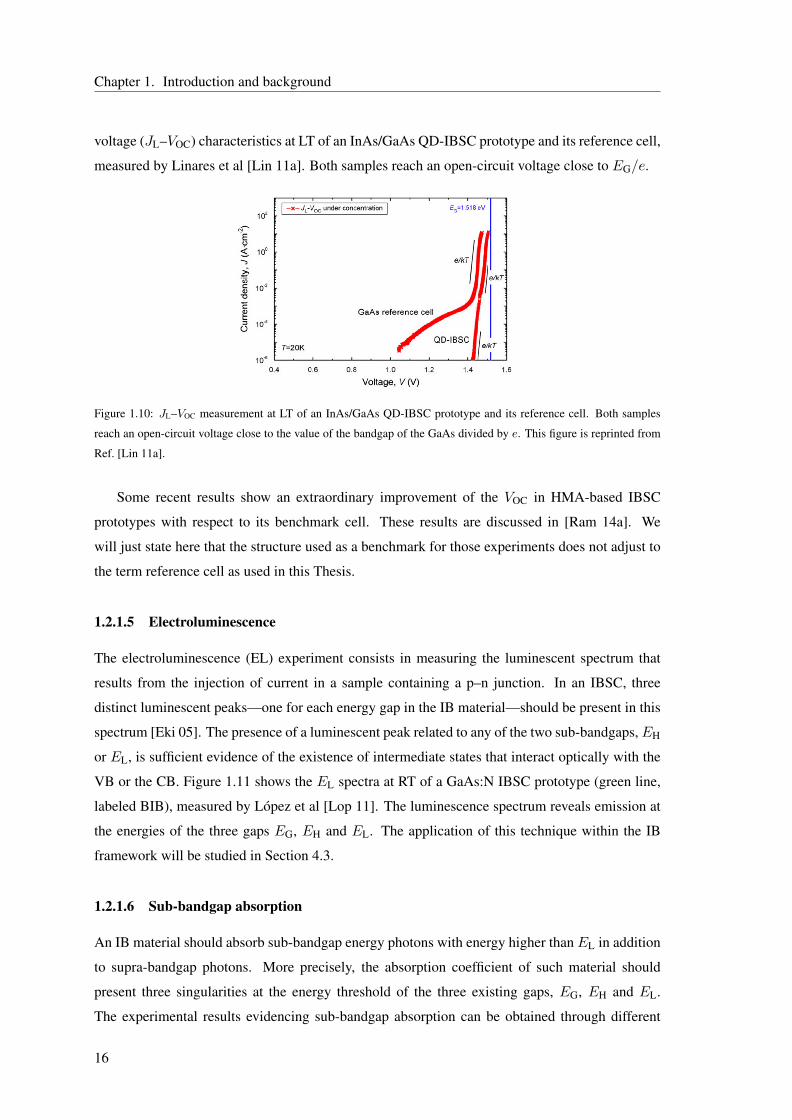
Voltage preservation is the capability of an IBSC to achieve a VOC higher that any of the two
sub-bandgaps related to the IB and, under sufficiently high light concentration, to reach a photo-
induced voltage close to EG/e. As opposed to the JSC, the VOC of an IBSC is not to be compared
with that of its reference cell for voltage preservation to be verified. The only condition is that the
output voltage is not limited by the presence of the IB; and one direct proof of that is to measure a
voltage higher than EH/e. Figure 1.9 shows the photo-generated current density vs. open-circuit
15
Chapter 1. Introduction and background
voltage (JL–VOC) characteristics at LT of an InAs/GaAs QD-IBSC prototype and its reference cell,
measured by Linares et al [Lin 11a]. Both samples reach an open-circuit voltage close to EG/e.
Figure 1.10: JL–VOC measurement at LT of an InAs/GaAs QD-IBSC prototype and its reference cell. Both samples
reach an open-circuit voltage close to the value of the bandgap of the GaAs divided by e. This figure is reprinted from
Ref. [Lin 11a].
Some recent results show an extraordinary improvement of the VOC in HMA-based IBSC
prototypes with respect to its benchmark cell. These results are discussed in [Ram 14a]. We
will just state here that the structure used as a benchmark for those experiments does not adjust to
the term reference cell as used in this Thesis.
1.2.1.5 Electroluminescence
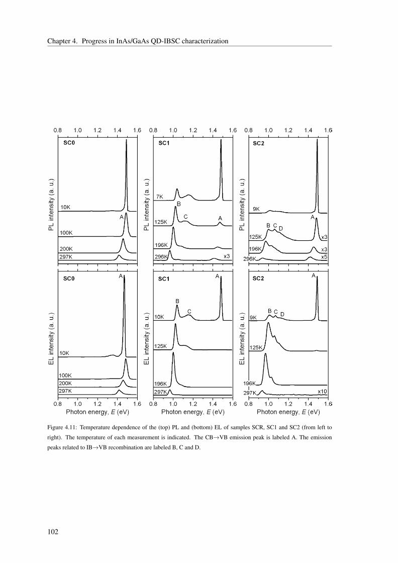
The electroluminescence (EL) experiment consists in measuring the luminescent spectrum that
results from the injection of current in a sample containing a p–n junction. In an IBSC, three
distinct luminescent peaks—one for each energy gap in the IB material—should be present in this
spectrum [Eki 05]. The presence of a luminescent peak related to any of the two sub-bandgaps,EH
or EL, is sufficient evidence of the existence of intermediate states that interact optically with the
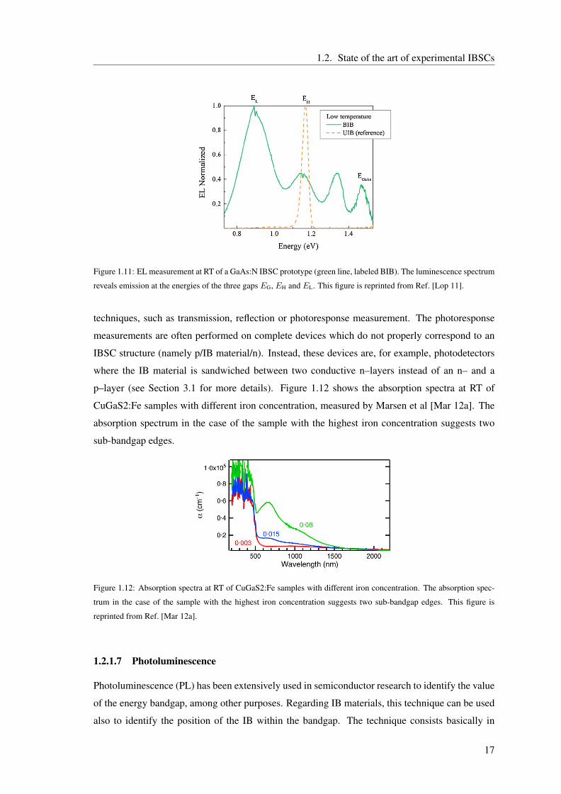
VB or the CB. Figure 1.11 shows the EL spectra at RT of a GaAs:N IBSC prototype (green line,
labeled BIB), measured by Lopez et al [Lop 11]. The luminescence spectrum reveals emission at
the energies of the three gaps EG, EH and EL. The application of this technique within the IB
framework will be studied in Section 4.3.
1.2.1.6 Sub-bandgap absorption
An IB material should absorb sub-bandgap energy photons with energy higher than EL in addition
to supra-bandgap photons. More precisely, the absorption coefficient of such material should
present three singularities at the energy threshold of the three existing gaps, EG, EH and EL.
The experimental results evidencing sub-bandgap absorption can be obtained through different
16
1.2. State of the art of experimental IBSCs
Figure 1.11: EL measurement at RT of a GaAs:N IBSC prototype (green line, labeled BIB). The luminescence spectrum
reveals emission at the energies of the three gaps EG, EH and EL. This figure is reprinted from Ref. [Lop 11].
techniques, such as transmission, reflection or photoresponse measurement. The photoresponse
measurements are often performed on complete devices which do not properly correspond to an
IBSC structure (namely p/IB material/n). Instead, these devices are, for example, photodetectors
where the IB material is sandwiched between two conductive n–layers instead of an n– and a
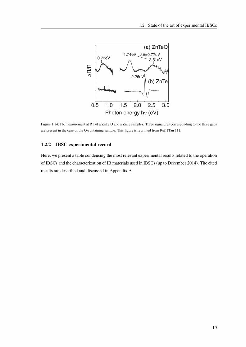
p–layer (see Section 3.1 for more details). Figure 1.12 shows the absorption spectra at RT of
CuGaS2:Fe samples with different iron concentration, measured by Marsen et al [Mar 12a]. The
absorption spectrum in the case of the sample with the highest iron concentration suggests two
sub-bandgap edges.
Figure 1.12: Absorption spectra at RT of CuGaS2:Fe samples with different iron concentration. The absorption spec-
trum in the case of the sample with the highest iron concentration suggests two sub-bandgap edges. This figure is
reprinted from Ref. [Mar 12a].
1.2.1.7 Photoluminescence
Photoluminescence (PL) has been extensively used in semiconductor research to identify the value
of the energy bandgap, among other purposes. Regarding IB materials, this technique can be used
also to identify the position of the IB within the bandgap. The technique consists basically in
17
Chapter 1. Introduction and background
illuminating the semiconductor with supra-bandgap light, which will be absorbed, and detect the
luminescent photons emitted by the material, resolving them spectrally. As for the EL case, three
distinct luminescent peaks, at the energies EG, EH and EL, should be resolved in the spectrum
of a proper IB material. Figure 1.13 shows the PL spectrum at RT of a CuInS2:Sn and a CuInS2
samples, measured by Yang et al [Yan 13]. The luminescence spectrum of the Sn-doped material
reveals an additional peak that can be identified as originated from radiative IB→VB electronic
relaxation. The application of this technique to within the IB framework will be studied in Section
4.3.
Figure 1.13: PL measurement at RT of a CuInS2:Sn and a CuInS2 samples. The luminescence spectrum of the Sn-
doped material reveals an additional peak that can be related to radiative IB→VB electronic relaxation. This figure is
reprinted from Ref. [Yan 13].
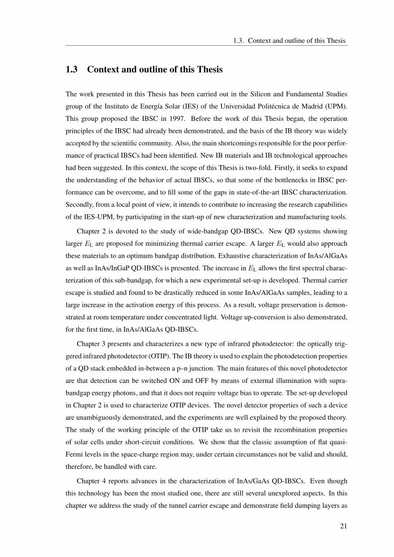
1.2.1.8 Photoreflectance
Photoreflectance (PR) is a modulation spectroscopy technique widely employed for characterizing
band-to-band transitions in semiconductors. The PR technique consists in measuring the change
in reflectivity of a sample by modulating an electric field acting on the sample. Usually, this
electric field is the field existing at the surface of the sample, and its modulation is achieved by
the absorption of photons from a modulated laser beam. Applied to the characterization of IB
materials, the three possible optical transitions depicted in Figure 1.2 could be identified. Figure
1.14 shows the PR spectrum at RT of a ZnTe:O and a ZnTe sample, measured by Tanaka et al
[Tan 11]. Three signatures corresponding to the three gaps are present in the case of the O-doped
sample.
18
1.2. State of the art of experimental IBSCs
Figure 1.14: PR measurement at RT of a ZnTe:O and a ZnTe samples. Three signatures corresponding to the three gaps
are present in the case of the O-containing sample. This figure is reprinted from Ref. [Tan 11].
1.2.2 IBSC experimental record
Here, we present a table condensing the most relevant experimental results related to the operation
of IBSCs and the characterization of IB materials used in IBSCs (up to December 2014). The cited
results are described and discussed in Appendix A.
19
Chapter1.
Introductionand
background
Sub-bandgap transitions Extra-photocurrent Voltage preservation
Material
Exp. techniqueAbsorption a PR PL EL SR / QE I–V TPPC VOC / JL–VOC
QD
In(Ga)As/Ga(N,P,Sb)As [Che 01, Sau 97, Phi 97,
Dur 98] e[Sun 98, Can 08, Fue 13] [Che 01, Sau 97, Phi 97,
Leo 95, Sun 98, Faf 99]
[Luq 05, Ram 11] b,e [Bai 12, Osh 08, Pop 08,
Alo 10, Lag 07a, Liu 12b,
Blo 09, Luq 04, Sab 11,
Zho 10, Tut 12, Nor 05,
Sug 12, Bea 14]
[Bai 12, Liu 12b, Blo 09,
Sab 11, Tut 12, Sug 12,
Bea 14]
[Mar 06a, Oka 11] e [Lin 11a, Ant 10b] b,e
GaSb/GaAs [Alo 07, Car 12, Tat 06] [Lag 07b, Alo 07, Car 12,
Wag 14, Hwa 14]
[Lag 07b, Car 12] [Hwa 14] e
InAs/AlGaAs [Phi 97] [Fue 13] [Phi 97, Leo 95, Siz 03] [Ram 12, Sch 12]
GaAs/AlGaAs [Wu 09] e [Wu 12, Wu 09, Bru 92] [Sca 13, Wu 12] [Sca 13] e
HMAZnTe:O [Tan 11, Ant 14] [Tan 11] [Wan 09] [Wan 09, Tan 11, Tan 13,
a By transmission, reflectance or photoresponse measurements.b Only in pure InAs/GaAs QDs.c Only with Fe.d Only with Mn.e All or part of the results were only obtained at cryogenic temperatures.
Table 1.1: Summary table relating the various experimental techniques that revealed IB phenomena to the IB materials used in IBSC. If reported experimental evidence exists, it is
referenced. A blank case appears otherwise.
20
1.3. Context and outline of this Thesis
1.3 Context and outline of this Thesis
The work presented in this Thesis has been carried out in the Silicon and Fundamental Studies
group of the Instituto de Energıa Solar (IES) of the Universidad Politecnica de Madrid (UPM).
This group proposed the IBSC in 1997. Before the work of this Thesis began, the operation
principles of the IBSC had already been demonstrated, and the basis of the IB theory was widely
accepted by the scientific community. Also, the main shortcomings responsible for the poor perfor-
mance of practical IBSCs had been identified. New IB materials and IB technological approaches
had been suggested. In this context, the scope of this Thesis is two-fold. Firstly, it seeks to expand
the understanding of the behavior of actual IBSCs, so that some of the bottlenecks in IBSC per-
formance can be overcome, and to fill some of the gaps in state-of-the-art IBSC characterization.
Secondly, from a local point of view, it intends to contribute to increasing the research capabilities
of the IES-UPM, by participating in the start-up of new characterization and manufacturing tools.
Chapter 2 is devoted to the study of wide-bandgap QD-IBSCs. New QD systems showing
larger EL are proposed for minimizing thermal carrier escape. A larger EL would also approach
these materials to an optimum bandgap distribution. Exhaustive characterization of InAs/AlGaAs
as well as InAs/InGaP QD-IBSCs is presented. The increase in EL allows the first spectral charac-
terization of this sub-bandgap, for which a new experimental set-up is developed. Thermal carrier
escape is studied and found to be drastically reduced in some InAs/AlGaAs samples, leading to a
large increase in the activation energy of this process. As a result, voltage preservation is demon-
strated at room temperature under concentrated light. Voltage up-conversion is also demonstrated,
for the first time, in InAs/AlGaAs QD-IBSCs.
Chapter 3 presents and characterizes a new type of infrared photodetector: the optically trig-
gered infrared photodetector (OTIP). The IB theory is used to explain the photodetection properties
of a QD stack embedded in-between a p–n junction. The main features of this novel photodetector
are that detection can be switched ON and OFF by means of external illumination with supra-
bandgap energy photons, and that it does not require voltage bias to operate. The set-up developed
in Chapter 2 is used to characterize OTIP devices. The novel detector properties of such a device
are unambiguously demonstrated, and the experiments are well explained by the proposed theory.
The study of the working principle of the OTIP take us to revisit the recombination properties
of solar cells under short-circuit conditions. We show that the classic assumption of flat quasi-
Fermi levels in the space-charge region may, under certain circumstances not be valid and should,
therefore, be handled with care.
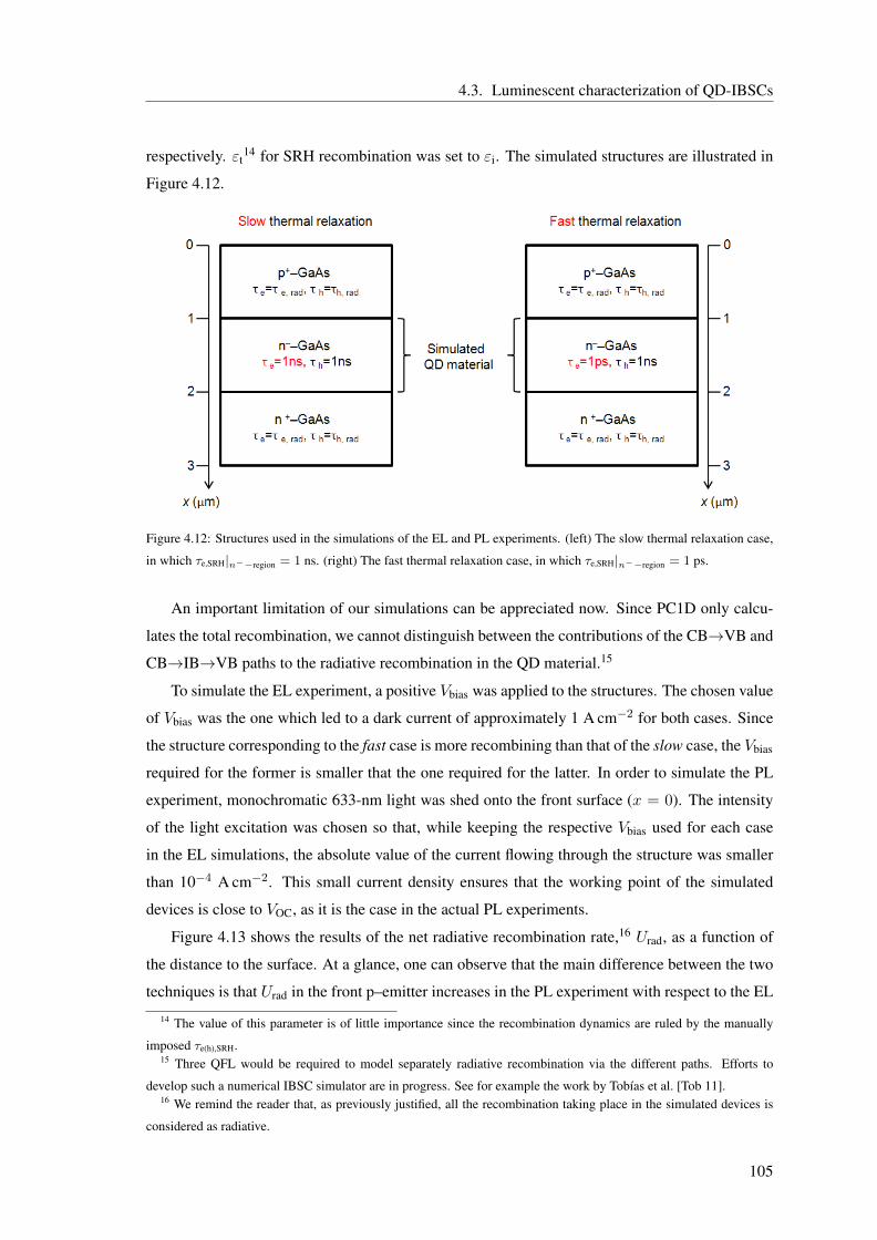
Chapter 4 reports advances in the characterization of InAs/GaAs QD-IBSCs. Even though
this technology has been the most studied one, there are still several unexplored aspects. In this
chapter we address the study of the tunnel carrier escape and demonstrate field dumping layers as
21
Chapter 1. Introduction and background
an effective way to prevent it. We describe a theory that relates the evolution of the tunnel carrier
escape as a function of the working voltage of the IBSC with the possibility of achieving voltage
preservation. Also, in this chapter we study luminescence of QD-IBSCs and its dependency with
temperature. For this, a photo- and electroluminescence set-up is developed. The low temperature
luminescent spectra of IBSCs that fulfill the voltage preservation principle is analyzed and shown
to be in agreement with the existence of an IB–CB quasi-Fermi level split.
In Chapter 5 we characterize the first QD-IBSC completely manufactured at the IES-UPM.
The material growth was made in a MBE reactor that was installed concurrently with the work of
this Thesis.
In Chapter 6 we draw the main conclusions of our and we indicate possible future lines of
work for which this Thesis opens the path.
Part of the work presented in this Thesis has been done in collaboration with the University of
Glasgow (UoG), the Instituto de Microelectronica de Madrid (IMM) of the Consejo Superior de
Investigaciones Cientıficas (CSIC) or the University College London (UCL).
22
Chapter 2
Research on wide-bandgap QD-IBSCs:
towards the realization of a practical
IBSC
2.1 Introduction
As introduced in Chapter 1, although the two operation principles of IBSCs have been demon-
strated in InAs/GaAs QD-IBSC prototypes, this has only been possible at LT because of the ex-
istence of thermal carrier escape. Thermal carrier escape is the thermally activated hopping of
carriers from confined states in the QDs to extended states in the host material. Thorough studies
have been performed [Faf 96,Xu 96,San 99,Le 03], leading to the a deep degree of understanding
of this mechanism. The general idea is that electrons interact with lattice phonons, thus obtaining
the necessary energy to escape from the potential well. There is clear evidence that thermal escape
is reduced if carrier confinement is increased. It has been found that thermal escape takes place
predominantly from the GSs. The explanation is that thermal carrier relaxation between confined
states is a faster process that thermal excitation out of the confined states. It is also believed that
the WL plays a role in the carrier thermal escape from the IB to the CB, acting as stepping stone to
reach the host material. This mechanism can be regarded as the reverse of the thermal relaxation
of carriers from the host material to the confined states via the WL [Tod 99]. It has been sug-
gested that the very thermal radiation of the semiconductor lattice can be a major cause of thermal
carrier escape, since at RT thermal photons are very abundant in the IB→CB transition range of
energies [Mar 06b, Luq 11]. Finally it is worth mentioning that some experiments suggest that
escape and capture processes occur in independent carriers (electrons or holes) and not in pairs or
excitons [Le 03].
23
Chapter 2. Research on wide-bandgap QD-IBSCs: towards the realization of a practical IBSC
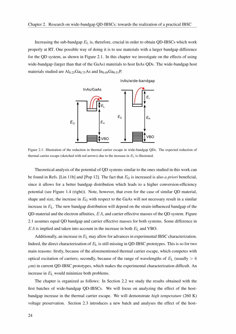
Increasing the sub-bandgap EL is, therefore, crucial in order to obtain QD-IBSCs which work
properly at RT. One possible way of doing it is to use materials with a larger bandgap difference
for the QD system, as shown in Figure 2.1. In this chapter we investigate on the effects of using
wide-bandgap (larger than that of the GaAs) materials to host InAs QDs. The wide-bandgap host
materials studied are Al0.25Ga0.75As and In0.49Ga0.51P.
Figure 2.1: Illustration of the reduction in thermal carrier escape in wide-bandgap QDs. The expected reduction of
thermal carrier escape (sketched with red arrows) due to the increase in EL is illustrated.
Theoretical analysis of the potential of QD systems similar to the ones studied in this work can
be found in Refs. [Lin 11b] and [Pop 12]. The fact that EG is increased is also a priori beneficial,
since it allows for a better bandgap distribution which leads to a higher conversion-efficiency
potential (see Figure 1.4 (right)). Note, however, that even for the case of similar QD material,
shape and size, the increase in EG with respect to the GaAs will not necessary result in a similar
increase in EL. The new bandgap distribution will depend on the strain-influenced bandgap of the
QD-material and the electron affinities, EA, and carrier effective masses of the QD system. Figure
2.1 assumes equal QD bandgap and carrier effective masses for both systems. Some difference in
EA is implied and taken into account in the increase in both EL and VBO.
Additionally, an increase inEL may allow for advances in experimental IBSC characterization.
Indeed, the direct characterization ofEL is still missing in QD-IBSC prototypes. This is so for two
main reasons: firstly, because of the aforementioned thermal carrier escape, which competes with
optical excitation of carriers; secondly, because of the range of wavelengths of EL (usually > 6
µm) in current QD-IBSC prototypes, which makes the experimental characterization difficult. An
increase in EL would minimize both problems.
The chapter is organized as follows: In Section 2.2 we study the results obtained with the
first batches of wide-bandgap QD-IBSCs. We will focus on analyzing the effect of the host-
bandgap increase in the thermal carrier escape. We will demonstrate high temperature (260 K)
voltage preservation. Section 2.3 introduces a new batch and analyses the effect of the host-
24
2.2. Impact on voltage preservation
bandgap increase inEL by presenting for the first time spectrally resolved two-photon photocurrent
measurements. Based on the experimental characterization we will sketch the band diagram of our
devices. Section 2.4 presents the first results of voltage up-conversion in IBSCs, demonstrating
that energy from two photons can be transferred and accumulated in an electron in a two-step
process via the IB. Also we will demonstrate RT voltage preservation in InAs/AlGaAs QD-IBSC
prototypes.
The work presented in this chapter has been made in collaboration with the University of
Glasgow (UoG) and the University College London (UCL).
2.2 Impact on voltage preservation
A connection between the IB and the CB (or the IB and the VB) not relying on radiative exchange
with the exterior hinders the QFL split of these two bands and prevents the preservation of the
voltage. Thermal carrier escape has an Arrhenius-like dependency with temperature. This means
that (1) the escape rate increases exponentially with temperature, and (2) an activation energy, Ea,
of this process can be defined. The higher the value of this parameter, the higher the temperature
needed for the process to take place.
The activation energy of thermal carrier escape in QDs has been sometimes roughly identified
with EL [Faf 96] but, in general, it has been found to be lower than this value [Fry 00], and
sometimes tentatively assigned to the difference (EES − EH) [Kap 99]1. Reported high measured
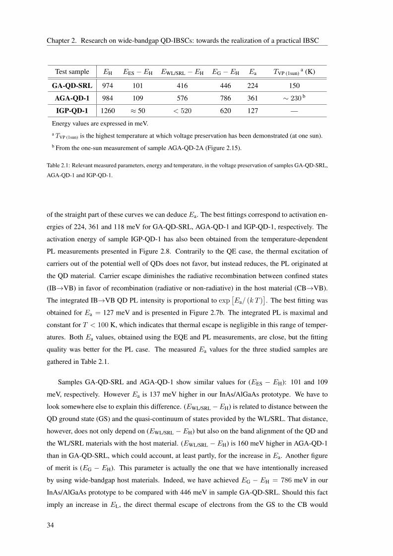
values for (EES −EH) are in the range of 90–100 meV [Faf 99]. In fact, this range coincides with
the reported high values of Ea in In(Ga)As/GaAs QDs, with two notable exceptions: activation
energies of 215 meV and as remarkably high as 480 meV were measured in Refs. [Faf 96] and [Le
03], respectively.
The effect of thermal carrier escape in the performance of QD-IBSCs was studied in Refs.
[Ant 10a] and [Ant 10b]. Strain relief layers (SRLs) were introduced after the growth of each
QD layer with the aim of increasing the dot height and minimizing local strain, obtaining a red-
shift of EH and an increase in both (EES − EH) and (EWL − EH). In those works, activation
energies of 115 and 224 meV were reported for samples without and with SRLs, respectively.
In both cases the measured Ea is higher than the value (EES − EH). The increase in Ea in the
sample with SRLs was partially attributed to the blue-shift of EWL. Temperature-dependent QE
measurements revealed that the thermally-assisted production of sub-bandgap photocurrent was
inhibited at around 100 and 150 K for the samples without and with SRLs, respectively. Closing
1 As a matter of fact, it is assigned to the energy difference between the ES1e and the GSe but, as justified in
Subsection 1.1.3, that difference can be approximated to (EES − EH), which depends on parameters that we can easily
characterize.
25
Chapter 2. Research on wide-bandgap QD-IBSCs: towards the realization of a practical IBSC
the loop, temperature-dependent VOC measurements revealed that, in the sample with SRL, voltage
preservation was achieved below 150 K. The conclusion is straightforward: an increase in Ea
reduces thermal carrier escape, removing that particular limitation to voltage preservation. In this
section, we will compare some of the experimental results obtained with our samples to those of
the aforementioned InAs/GaAs QD-IBSC with SRLs, to which we will refer as GA-QD-SRL. The
layer structure of sample GA-QD-SRL is sketched in Figure 4.2 (sample SC1).
2.2.1 First InAs/AlGaAs and InAs/InGaP batches
We will now present our first wide-bandgap QD-IBSC prototypes. We have chosen to use Al-
GaAs and InGaP as host materials because they exhibit direct bandgap2 and can be grown lattice-
matched with GaAs. In addition, the suitability of both alloys for solar-cell fabrication has been
previously demonstrated [Vir 85,Tak 97]. No previous reports have been made on InAs/AlGaAs or
InAs/InGaP QD-IBSCs. Nonetheless, there exists relevant characterization work on InAs/AlGaAs
QDs and, to a lesser extent, on InAs/InGaP QDs.
The growth by MBE of InAs/AlxGa1-xAs QDs with x ≤ 0.33 is in a mature state. The inclu-
sion of Al in the barrier produces a blue shift of EH of around 0.08–0.12 eV, for x = 0.15 [Phi 97]
and x = 0.3 [Pol 99, Sch 08], with respect to the InAs/GaAs benchmark, in which it usually lies
around 1.08–1.12 eV. In Ref. [Siz 03] EH was varied between 1.03 and 1.29 eV by changing the
amount of the deposited InAs on Al0.3Ga0.7As. In that same work EH = 1 eV was obtained by
capping the dots with a thin InGaAs layer. The inclusion of Al in the host produces also a small
increase in EL, as reported in Ref. [Phi 97] (20 meV) and Ref. [Che 01] (45 meV), for x = 0.15
and x = 0.33, respectively. In all cases, the reported values of EL are smaller or equal to 0.2 eV.
There are some studies on InAs QDs on In0.49Ga0.51P latticed-matched to GaAs, grown by
MBE [Ama 01, Sug 13] or by MOVPE [For 13]. In Ref. [For 13] the QDs resulted larger than the
typical size for InAs/GaAs, which is an undesirable effect for IBSC purposes. In Ref. [Ama 01]
it was found that the critical thickness3 for QD nucleation of InAs over InGaP is 0.15 monolayers
(MLs), far less than for the InAs/GaAs case. The critical thickness increases if thin GaAs barriers
are included before and after the dots. It was also found that the GaAs barriers avoid intermixing
between the InGaP spacers and the InAs QDs. Said intermixing leads to the presence of InGaAsP
alloys and modifies the optical properties of the dots. Motivated by those discoveries, in Ref.
[Sug 13] InAs/InGaP QDs with thin GaAs barriers were grown. A red-shift of EH, from 1.4
eV to 1.2 eV, with increasing thickness of the barriers was measured. EL has been measured in
InAs/InGaP QD-based n–i–n photodetectors grown by MOVPE [Jia 04, Kim 98]. In that work,
response ranges of approximately 0.2–0.3 eV were reported.
2 For an Al content below 0.45, in the case of AlGaAs.3 The reader is referred to Chapter 5 for more information about this an other MBE-grown QD concepts.
26
2.2. Impact on voltage preservation
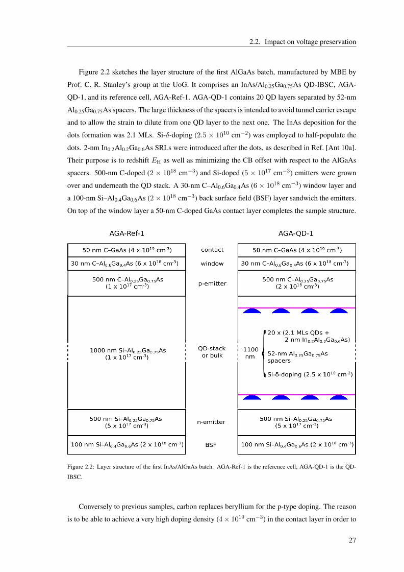
Figure 2.2 sketches the layer structure of the first AlGaAs batch, manufactured by MBE by
Prof. C. R. Stanley’s group at the UoG. It comprises an InAs/Al0.25Ga0.75As QD-IBSC, AGA-
QD-1, and its reference cell, AGA-Ref-1. AGA-QD-1 contains 20 QD layers separated by 52-nm
Al0.25Ga0.75As spacers. The large thickness of the spacers is intended to avoid tunnel carrier escape
and to allow the strain to dilute from one QD layer to the next one. The InAs deposition for the
dots formation was 2.1 MLs. Si-δ-doping (2.5 × 1010 cm−2) was employed to half-populate the
dots. 2-nm In0.2Al0.2Ga0.6As SRLs were introduced after the dots, as described in Ref. [Ant 10a].
Their purpose is to redshift EH as well as minimizing the CB offset with respect to the AlGaAs
spacers. 500-nm C-doped (2 × 1018 cm−3) and Si-doped (5 × 1017 cm−3) emitters were grown
over and underneath the QD stack. A 30-nm C–Al0.6Ga0.4As (6 × 1018 cm−3) window layer and
a 100-nm Si–Al0.4Ga0.6As (2× 1018 cm−3) back surface field (BSF) layer sandwich the emitters.
On top of the window layer a 50-nm C-doped GaAs contact layer completes the sample structure.
Figure 2.2: Layer structure of the first InAs/AlGaAs batch. AGA-Ref-1 is the reference cell, AGA-QD-1 is the QD-
IBSC.
Conversely to previous samples, carbon replaces beryllium for the p-type doping. The reason
is to be able to achieve a very high doping density (4× 1019 cm−3) in the contact layer in order to
27
Chapter 2. Research on wide-bandgap QD-IBSCs: towards the realization of a practical IBSC
obtain low-resistance ohmic contacts.4 AGA-Ref-1 shares the structure of AGA-QD-1 except for
the QD stack, which is replaced by an equally thick Si–Al0.25Ga0.75As layer with a Si-doping of
(1 × 1017 cm−3). Metal ohmic contacts were made by Dr. C. D. Farmer by thermal evaporation
and annealing, using standard photolithographic methods. The contact layer was not removed after
metalization.
Figure 2.3 shows several transmission electron microscopy (TEM) micrographs of sample
AGA-QD-1. The images were obtained using a transmission electron microscope Jeol 1200 EX.
Figure 2.3a shows a bright-field cross-sectional TEM (BF-XTEM) of the top QD layers and the
overgrown p–emitter. The n–emitter (labeled ’base’) and the overgrown bottom QD layers are
shown in Figure 2.3b. It can be appreciated that the dots have nucleated in all the layers. Also, the
growth of the dots is not vertically correlated, which indicates that the thick (50 nm) spacers have
diluted part of the strain. The effective dilution of the strain is also appreciated in the p–emitter,
which seems to be free of dislocations.
The QD morphology has been analyzed by high-angle annular dark-field scanning TEM (HAADF-
STEM) at the University of Cadiz. Figure 2.3c shows a small region of two consecutive dot layers.
With this image we can get some idea of what the dot size and shape, and the interdot spacing are.
Figure 2.3d shows a single QD. The different alloys present in the image are indicated: InAs in the
QD and WL, InAlGaAs in the SRL, and AlGaAs in the spacers. The different alloys are identified
by different image intensities according to their effective atomic number. Profuse measurements
of the dot dimensions, according to the simple dot-geometry sketched in Figure 2.3e, have been
carried out. Two heights, a and b, and two widths, c and d, are defined. b and d include the InAl-
GaAs capping in the dot size, whereas a and c do not. The values found for these parameters are:
a = 6.2± 1.2 nm, b = 6.6± 1 nm, c = 20.4± 2.1 nm and d = 24.2± 5.2 nm.
Figure 2.4 sketches the layer structure of the first InGaP batch, manufactured by MBE by the
group of Prof. H. Liu at the UCL. It comprises an InAs/In0.49Ga0.51P QD-IBSC, IGP-QD-1, and
its reference cell, IGP-Ref-1. IGP-QD-1 contains 20 QD layers separated by 50-nm In0.49Ga0.51P
spacers. The large thickness of the spacers is intended to avoid tunnel carrier escape and allow for
the strain to dilute from one QD layer to the next one. The InAs deposition for the dots formation
was 2.1 MLs. The QD stack is not intentionally doped. This has been made for practicality: the
growth of InAs/InGaP QDs is not yet fully mastered, so the purpose was to obtain a first prototype
which could be studied, even if its design was not optimized. The dots are sandwiched between
two thin (3 nm before InAs deposition and 6 nm after the dot formation) Al0.33Ga0.67As barriers.
The objective of these barriers is to accommodate the dot formation, avoiding intermixing between
4 IBSC is, as of today, considered a CPV-oriented technology, since the maximum benefits of the IB are predicted un-
der high solar concentration. CPV cells require very-low-resistive contacts, in order not to suffer from series-resistance
losses.
28
2.2. Impact on voltage preservation
Figure 2.3: TEM micrographs of sample AGA-QD-1. (a) BF-XTEM image of the top QD layers and the overgrown
p–emitter. (b) BF-XTEM image of the bottom QD layers and the n–emitter (labeled ’base’). (c) HAADF-STEM image
of a small region containing QDs. (d) HAADF-STEM image of a single QD. The different alloys present in the image
are labeled. (e) Sketch of the approximative QD shape defining two heights, a and b, and two widths, c and d. These
images are a courtesy of the group of Prof. S. Molina, University of Cadiz.
the InAs islands and the overgrown InGaP. The upper layer is 6-nm thick in order to completely
cover the dots.
200-nm Si-doped (2×1018 cm−3) and 500-nm Be-doped (1×1017 cm−3) emitters were grown
over and underneath the QD stack. A 30-nm Si–In0.5Ga0.33Al0.17P (5× 1018 cm−3) window layer
and a 30-nm Be–In0.5Ga0.33Al0.17P (5 × 1017 cm−3) BSF layer sandwich the emitters. On top of
the window layer a 50-nm, Si-doped GaAs contact layer (5 × 1018 cm−3) completes the sample
structure. IGP-Ref-1 shares the structure of IGP-QD-1 except for the QD stack, which is replaced
by an equally thick In0.49Ga0.51P layer. Metal ohmic contacts were made at the IES by thermal
evaporation and annealing using standard photolithographic methods. The contact layer was not
removed after metalization.
29
Chapter 2. Research on wide-bandgap QD-IBSCs: towards the realization of a practical IBSC
Figure 2.4: Layer structure of the first InAs/InGaP batch. IGP-Ref-1 is the reference cell, IGP-QD-1 is the QD-IBSC.
2.2.2 Characterization of thermal carrier escape and voltage preservation
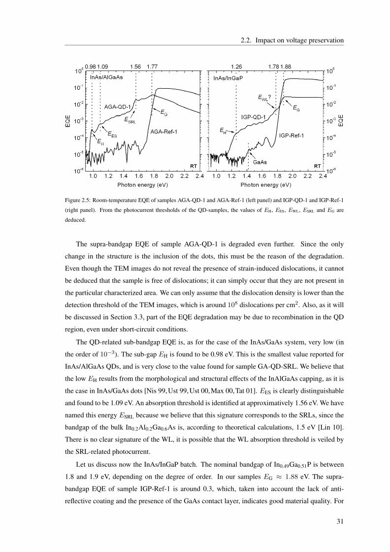
Figure 2.5 presents the EQE results obtained at RT for both batches. The left panel shows the
InAs/AlGaAs case and the right panel shows the InAs/InGaP case. We will analyze these results
highlighting the relevant features for QD-IBSCs and trying to identify the energy values that may
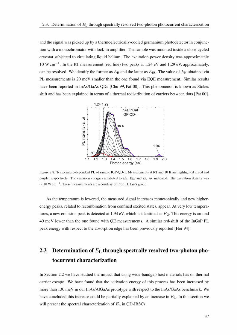
play a role in thermal carrier escape.
Let us begin with the InAs/AlGaAs batch. The nominal bandgap at RT of Al0.25Ga0.75As is
1.74 eV. From our measurements we assign the approximative values 1.77 and 1.78 eV to EG for
the QD and the reference samples, respectively, which indicates that the actual Al content may
be slightly higher than intended. The supra-bandgap EQE of sample AGA-Ref-1 is below 0.1
for all photon energies. This low response is only partly explained by the lack of anti-reflective
coating and the presence of the GaAs contact layer, whose absorption does not contribute to the
photocurrent. Poor electronic material properties account for the remaining reduction. The EQE is
particularly low for high energies (note the logarithmic scale). One possibility is that the C-doping
of the emitter introduces defects which increase carrier recombination. For sub-bandgap energies
there is no measurable response.
30
2.2. Impact on voltage preservation
Figure 2.5: Room-temperature EQE of samples AGA-QD-1 and AGA-Ref-1 (left panel) and IGP-QD-1 and IGP-Ref-1
(right panel). From the photocurrent thresholds of the QD-samples, the values of EH, EES, EWL, ESRL and EG are
deduced.
The supra-bandgap EQE of sample AGA-QD-1 is degraded even further. Since the only
change in the structure is the inclusion of the dots, this must be the reason of the degradation.
Even though the TEM images do not reveal the presence of strain-induced dislocations, it cannot
be deduced that the sample is free of dislocations; it can simply occur that they are not present in
the particular characterized area. We can only assume that the dislocation density is lower than the
detection threshold of the TEM images, which is around 108 dislocations per cm2. Also, as it will
be discussed in Section 3.3, part of the EQE degradation may be due to recombination in the QD
region, even under short-circuit conditions.
The QD-related sub-bandgap EQE is, as for the case of the InAs/GaAs system, very low (in
the order of 10−3). The sub-gap EH is found to be 0.98 eV. This is the smallest value reported for
InAs/AlGaAs QDs, and is very close to the value found for sample GA-QD-SRL. We believe that
the low EH results from the morphological and structural effects of the InAlGaAs capping, as it is
the case in InAs/GaAs dots [Nis 99,Ust 99,Ust 00,Max 00,Tat 01]. EES is clearly distinguishable
and found to be 1.09 eV. An absorption threshold is identified at approximatively 1.56 eV. We have
named this energy ESRL because we believe that this signature corresponds to the SRLs, since the
bandgap of the bulk In0.2Al0.2Ga0.6As is, according to theoretical calculations, 1.5 eV [Lin 10].
There is no clear signature of the WL, it is possible that the WL absorption threshold is veiled by
the SRL-related photocurrent.
Let us discuss now the InAs/InGaP batch. The nominal bandgap of In0.49Ga0.51P is between
1.8 and 1.9 eV, depending on the degree of order. In our samples EG ≈ 1.88 eV. The supra-
bandgap EQE of sample IGP-Ref-1 is around 0.3, which, taken into account the lack of anti-
reflective coating and the presence of the GaAs contact layer, indicates good material quality. For
31
Chapter 2. Research on wide-bandgap QD-IBSCs: towards the realization of a practical IBSC
below bandgap energies, the EQE falls drastically, but is still measurable until 1.42 eV. This sub-
bandgap EQE reveals the existence of photocurrent originating from the GaAs substrate, which
indicates that the BSF layer does not disconnect completely the solar cell structure from the low-
bandgap substrate [Mar 13b]. Moreover, the oscillations in the sub-bandgap EQE suggest an
interference effect that is probably due to the combination of thin layers of different materials
within the solar cell.
The supra-bandgap EQE of sample IGP-QD-1 is one order of magnitude lower than that of
its reference cell. It is likely that the inclusion of QDs have degraded the quality of the grown
material, both in the QD stack and in the front n–emitter. Unfortunately, we do not have TEM
measurements of sample IGP-QD-1, so we cannot graphically assess the material quality. It may
be that the 50-nm thick spacers are not enough and the accumulated strain ends up provoking
threading dislocations. Studies of more samples are needed, but it seems that for InAs/InGaP as
well as in for InAs/AlGaAs, strain-compensation techniques may be necessary to preserve good
material quality and avoid, to a high extent, additional non-radiative recombination.5
The sub-bandgap EQE is, again in this case, very low (10−4–10−3). EH is not clearly distin-
guishable but lies around 1.26 eV. This value is supported by the PL measurement at RT presented
in Figure 2.8 (see the discussion later on). The interference effect mentioned above is also present
in the QD sample. From the EQE measurements, we cannot identify the energy EES, however
from the PL measurements we can assign EES − EH ≈ 50 meV. Likewise we cannot precisely
identify the threshold EWL. A change of slope is observed between the abrupt decay below EG
and the QD-related photocurrent. This change of slope begins approximatively at 1.78 eV; we will
tentatively assign this value as upper bound to EWL. The bulk Al0.53Ga0.47As has a theoretical
bandgap of 1.84 eV, which should be larger in our thin barriers. The barriers do not seem to have
any impact on the photocurrent spectrum.
The characterized energy values are gathered in Table 2.1 together with the same parameters
for sample GA-QD-SRL. Because this section focuses on the impact of the wide-bandgap host in
Ea, Table 2.1 presents the differences between those parameters and EH, which will help in the
discussion. The reader will notice that we treat equally EWL and ESRL. In fact, the difference
in nomenclature responds to whether the characterized absorption threshold is due to the WL or
the quaternary QD capping. However, regarding thermal escape, both parameters should have a
similar impact, since in both cases we are dealing with QWs. It is the quasi-continuum of states
inherent to this type of structures which provides an extra path for carriers to thermally escape to
the host.
5 These techniques have proven effective for the InAs/GaAs system, where samples with no carrier collection degra-
dation have been demonstrated [Hub 08].
32
2.2. Impact on voltage preservation
Figure 2.6: Temperature-dependent EQE of samples GA-QD-SRL, AGA-QD-1 and IGP-QD-1. The thick solid lines
represent the RT measurements. Other temperature values which are relevant for the discussion are indicated. The
energy parameters gathered in Table 2.1 are indicated by dotted lines. For IGP-QD-1 (EES − EH) is deduced from the
PL measurements presented in Figure 2.8 and not by the EQE measurements of Figure 2.5.
To obtain the activation energy in our samples we have performed temperature-dependent EQE
measurements, shown in Figure 2.6. For comparison, similar measurements reported in [Ant 10a]
for GA-QD-SRL are presented. We will focus only on the sub-bandgap part of the graphs. The
measurement at RT is plotted with a thicker line. Other temperature values are indicated in the
figure to support the discussion. In all samples the EQE diminishes for lower temperatures but the
diminution rate is different in each sample. To illustrate this, let us give some examples. The EQE
at EH is reduced by two orders of magnitude from RT to 160 K in sample GA-QD-SRL. A similar
reduction factor is observed in sample AGA-QD-1 when going from RT to 220 K. In sample
IGP-QD-1 there is only one order of magnitude of EQE reduction from RT to 150 K. Another
difference can be established: for the lowest temperatures the sub-bandgap QE attributed to the
QDs has disappeared for samples GA-QD-SRL and AGA-QD-1, but remains for sample IGP-QD-
1 even at temperatures as low as 11 K, at which the thermal energy of the lattice is minimal. This
indicates the presence of tunnel escape in this sample. Both AGA-QD-1 and IGP-QD-1 have 20
QD layers with around 50 nm-thick spacers. We can deduce that this spacer thickness is enough to
totally suppress tunnel carrier escape for the InAs/AlGaAs case but not for the InAs/InGaP case,
at least under short-circuit conditions. This may be due to the fact the EG is larger in the latter
case than in the former, which implies a larger value of the built-in voltage as well.6
Ea can be obtained from the following relationship: QE ∝ exp[−Ea/ (k T )
], where k is the
Boltzmann constant. Figure 2.7a plots ln(EQE) vs T for the three studied samples. From the slope
6 Refer to Section 4.2 for a detailed discussion of this statement.
33
Chapter 2. Research on wide-bandgap QD-IBSCs: towards the realization of a practical IBSC
Test sample EH EES − EH EWL/SRL − EH EG − EH Ea TVP (1sun)a (K)
GA-QD-SRL 974 101 416 446 224 150
AGA-QD-1 984 109 576 786 361 ∼ 230 b
IGP-QD-1 1260 ≈ 50 < 520 620 127 —
Energy values are expressed in meV.a TVP (1sun) is the highest temperature at which voltage preservation has been demonstrated (at one sun).b From the one-sun measurement of sample AGA-QD-2A (Figure 2.15).
Table 2.1: Relevant measured parameters, energy and temperature, in the voltage preservation of samples GA-QD-SRL,
AGA-QD-1 and IGP-QD-1.
of the straight part of these curves we can deduce Ea. The best fittings correspond to activation en-
ergies of 224, 361 and 118 meV for GA-QD-SRL, AGA-QD-1 and IGP-QD-1, respectively. The
activation energy of sample IGP-QD-1 has also been obtained from the temperature-dependent
PL measurements presented in Figure 2.8. Contrarily to the QE case, the thermal excitation of
carriers out of the potential well of QDs does not favor, but instead reduces, the PL originated at
the QD material. Carrier escape diminishes the radiative recombination between confined states
(IB→VB) in favor of recombination (radiative or non-radiative) in the host material (CB→VB).
The integrated IB→VB QD PL intensity is proportional to exp[Ea/ (k T )
]. The best fitting was
obtained for Ea = 127 meV and is presented in Figure 2.7b. The integrated PL is maximal and
constant for T < 100 K, which indicates that thermal escape is negligible in this range of temper-
atures. Both Ea values, obtained using the EQE and PL measurements, are close, but the fitting
quality was better for the PL case. The measured Ea values for the three studied samples are
gathered in Table 2.1.
Samples GA-QD-SRL and AGA-QD-1 show similar values for (EES − EH): 101 and 109
meV, respectively. However Ea is 137 meV higher in our InAs/AlGaAs prototype. We have to
look somewhere else to explain this difference. (EWL/SRL−EH) is related to distance between the
QD ground state (GS) and the quasi-continuum of states provided by the WL/SRL. That distance,
however, does not only depend on (EWL/SRL − EH) but also on the band alignment of the QD and
the WL/SRL materials with the host material. (EWL/SRL − EH) is 160 meV higher in AGA-QD-1
than in GA-QD-SRL, which could account, at least partly, for the increase in Ea. Another figure
of merit is (EG − EH). This parameter is actually the one that we have intentionally increased
by using wide-bandgap host materials. Indeed, we have achieved EG − EH = 786 meV in our
InAs/AlGaAs prototype to be compared with 446 meV in sample GA-QD-SRL. Should this fact
imply an increase in EL, the direct thermal escape of electrons from the GS to the CB would
34
2.2. Impact on voltage preservation
be consequently reduced. We will demonstrate in Section 2.3 that EL has been indeed largely
increased.
As for the InAs/InGaP prototype, (EG − EH) is higher and (EWL/SRL − EH) is, at least, not
smaller than in the InAs/GaAs case. The reason for the low measured activation energy, almost
100 meV smaller in the former than in the latter, is explained in terms of a decrease of 50 meV in
(EES − EH) and, probably, a higher density of confined states between the GS and the CB.
We have measured the temperature-dependence of the open-circuit voltage of our samples. As
previously discussed, thermal escape, whether of thermal or tunnel nature, imposes a limitation to
the VOC of IBSCs. An increase in Ea should be accompanied by an increase in the temperature at
which the thermal-escape-related limitation to the VOC is suppressed. Figure 2.7c plots the VOC vs
T results. For comparison, the respective results for sample GA-QD-SRL (reported in [Ant 10a])
is also plotted. The VOC measurements are represented with empty symbols. To help the discussion
we also present, with filled symbols, the measured values of EH (divided by e) for each sample
at different temperatures. The measured values of EG/e at 10 K for the different host materials,
obtained by photocurrent measurements, are indicated with dashed lines.
Samples GA-QD-SRL (triangles) and AGA-QD-1 (stars) were excited with a 632.5-nm (1.96
eV) He-Ne laser. The VOC of sample AGA-QD-1 increases from 0.84 V at RT to 1.83 V at 10 K,
demonstrating, for the first time, voltage preservation in the InAs/AlGaAs system. Moreover, VOC
exceeds EH at around 260 K, to be compared with 150 K in the case of sample GA-QD-SRL. It
must be noted that sample AGA-QD-1 was measured under an equivalent excitation of 15 suns,
while the excitation was approximatively one sun for the case of GA-QD-SRL. Nonetheless, we
shall see later on how measurements performed on similar InAs/AlGaAs samples under one-sun
excitation reveal voltage preservation at 230 K (see Figure 2.15). Note that in Figure 2.6 the EQE
at the energy EH has almost vanished at T = 220 K in sample AGA-QD-1, while T = 140 K
is required for this to happen in sample GA-QD-SRL. As expected, the increase in Ea (from 224
meV to 361 meV) leads to an increase (of 80 K) in the temperature of proper operation of IBSCs.
These temperature values are gathered in Table 2.1.
Sample IGP-QD-1 (circles) was excited with a 532-nm (2.33 eV) laser diode. We used higher
illumination energy than for the AlGaAs samples because of the larger bandgap of the InGaP. The
equivalent excitation intensity was approximatively 0.25 suns. The VOC of this sample increases
linearly from RT (0.54 V) to 150 K (0.92 V), it then reaches a plateau and decreases slowly from
100 K to 40 K. From 40 K to 10 K it decreases abruptly. We do not have an explanation for this
erratic behavior, especially below 100 K. The total recombination of a solar cell decreases with
temperature so the VOC should increase monotonically with decreasing temperature until it reaches
a maximum. It is possible that one of the metal contacts becomes non-ohmic at low temperatures
forming a Schottky diode with the semiconductor. In any case, for T > 150 K the temperature
35
Chapter 2. Research on wide-bandgap QD-IBSCs: towards the realization of a practical IBSC
Figure 2.7: Activation energies and temperature-dependent VOC of samples GA-QD-SRL (triangles), AGA-QD-1 (stars)
and IGP-QD-1 (circles). (a) Ea obtained by QE measurements. (b) Ea obtained by PL measurements. (c) VOC vs T .
The measured values of EH for the three samples are plotted with filled symbols. The bandgaps at 10 K of the different
host materials are indicated with dashed lines.
dependence of VOC seems to follow the same trend that the InAs/GaAs and the InAs/AlGaAs
samples, except that, in this case, the VOC is much lower than EH (> 1.3 eV). To discard that
the non-fulfilling of the voltage preservation principle is due to the low excitation intensity, we
have repeated the experiment using the He-Ne laser in the high-temperature range – for lower
temperatures the laser energy is lower than EG – providing an equivalent excitation intensity of
15 suns. The maximum measured VOC is 1.02 V at T = 200 K. Since the activation energy of
sample IGP-QD-1 is 100 meV lower than that of sample GA-QD-SRL, we would expect voltage
preservation to be achieved only for temperatures lower than 150 K, and probably lower than 100
K. We could not verify voltage preservation in our sample.
Finally, Figure 2.8 shows temperature-dependent PL measurements performed on sample IGP-
QD-1. A 532-nm continuous wave-diode-pumped solid-state laser was used to excite the sample
36
2.3. Determination of EL through spectrally resolved two-photon photocurrent characterization
and the signal was picked up by a thermoelectrically-cooled germanium photodetector in conjunc-
tion with a monochromator with lock-in amplifier. The sample was mounted inside a close-cycled
cryostat subjected to circulating liquid helium. The excitation power density was approximately
10 W cm−1. In the RT measurement (red line) two peaks at 1.24 eV and 1.29 eV, approximately,
can be resolved. We identify the former as EH and the latter as EES. The value of EH obtained via
PL measurements is 20 meV smaller than the one found via EQE measurement. Similar results
have been reported in InAs/GaAs QDs [Chu 99, Pat 00]. This phenomenon is known as Stokes
shift and has been explained in terms of a thermal redistribution of carriers between dots [Pat 00].
Figure 2.8: Temperature-dependent PL of sample IGP-QD-1. Measurements at RT and 10 K are highlighted in red and
purple, respectively. The emission energies attributed to EH, EES and EG are indicated. The excitation density was
∼ 10 W cm−1. These measurements are a courtesy of Prof. H. Liu’s group.
As the temperature is lowered, the measured signal increases monotonically and new higher-
energy peaks, related to recombination from confined excited states, appear. At very low tempera-
tures, a new emission peak is detected at 1.94 eV, which is identified as EG. This energy is around
40 meV lower than the one found with QE measurements. A similar red-shift of the InGaP PL
peak energy with respect to the absorption edge has been previously reported [Hor 94].
2.3 Determination of EL through spectrally resolved two-photon pho-
tocurrent characterization
In Section 2.2 we have studied the impact that using wide-bandgap host materials has on thermal
carrier escape. We have found that the activation energy of this process has been increased by
more than 130 meV in our InAs/AlGaAs prototype with respect to the InAs/GaAs benchmark. We
have concluded this increase could be partially explained by an increase in EL. In this section we
will present the spectral characterization of EL in QD-IBSCs.
37
Chapter 2. Research on wide-bandgap QD-IBSCs: towards the realization of a practical IBSC
Although EL has been spectrally resolved in QD materials, the optical activity of EL in QD-
IBSCs has only been demonstrated for broadband infrared (IR) illumination, so far [Mar 06a,
Oka 11, Sca 13, Hwa 14]. Being able to routinely characterize the three bandgaps of an IBSC
is important in order to provide constant experimental feedback to the IB-material design and
fabrication. Thus, for current InAs/GaAs prototypes it is not only the fact that EG is low (effec-
tively around 1.2 eV) which lowers the potential efficiency, but also that the bandgap distribution
(EH ∼ 1–1.1 eV, EL ∼ 0.2–0.1 eV) is not optimal to efficiently exploit the sunlight spectrum.
2.3.1 Second InAs/AlGaAs batch
Motivated by the good results obtained for sample AGA-QD-1 in Section 2.2, we have fabricated a
new InAs/AlGaAs batch. With this new batch we aimed to improve the response to supra-bandgap
light. For that, we have introduced two changes with respect to the first batch. The p–doping
has been done with beryllium instead of carbon. Carbon has only been used in the GaAs contact
layer, where the highest doping concentration is needed. This change is intended to avoid possible
defects introduced by the C-doping of the active layers of the devices. In order to reduce the
impact of accumulated strain in the crystal growth, we have increased the thickness of the AlGaAs
spacers. Also, the new samples contain fewer QD layers. These changes are highlighted in red
Figure 2.9.
Figure 2.9 sketches the layer structure of the second AlGaAs batch, manufactured by MBE
by Prof. C. R. Stanley and Dr. M. J. Steer at the UoG. It comprises two InAs/Al0.25Ga0.75As
QD-IBSCs, AGA-QD-2A and AGA-QD-2B, and their reference cell, AGA-Ref-2. AGA-QD-2A
and AGA-QD-2B contain 5 and 10 QD layers, respectively, separated by 82-nm Al0.25Ga0.75As
spacers. The InAs deposition for the dots formation was 2.2 MLs. Si-δ-doping (2.5× 1010 cm−2)
was employed to half-populate the dots. 2-nm In0.2Al0.2Ga0.6As SRLs were introduced after the
dots. 500-nm Be-doped (2× 1018 cm−3) and Si-doped (5× 1017 cm−3) emitters were grown over
and underneath the QD stack. A 30-nm Be–Al0.6Ga0.4As (6 × 1018 cm−3) window layer and a
100-nm Si–Al0.4Ga0.6As (2×1018 cm−3) BSF layer sandwich the emitters. On top of the window
layer a 50-nm, C-doped (4× 1019 cm−3) GaAs contact layer completes the sample structure.
AGA-Ref-2 shares the structure of AGA-QD-2A and AGA-QD-2B except for the QD stack,
which is replaced by an equally thick Si–Al0.25Ga0.75As layer with such Si-doping as to reproduce
the volumetric doping level of the QD stack of sample AGA-QD-2B. Unintentionally, the doping
level of the Si–emitter of AGA-Ref-2 is 1×1017 cm−3 (instead of 5×1017 cm−3). This, however,
should not produce a noticeable difference in the sample performance. Metal ohmic contacts were
made by Dr. C. D. Farmer by thermal evaporation and annealing, using standard photolithographic
methods. The contact layer was not removed after metalization.
38
2.3. Determination of EL through spectrally resolved two-photon photocurrent characterization
Figure 2.9: Layer structure of the second InAs/AlGaAs batch. AGA-Ref-2 is the reference cell, AGA-QD-2A and
AGA-QD-2B are QD-IBSCs. The changes with respect to the first batch (Figure 2.2) are highlighted in red.
Figure 2.10 shows two TEM micrographs performed on samples AGA-QD-2B. The images
were obtained using a transmission electron microscope Jeol 1200 EX working at 120 KV. The
left-hand side of the figure is a dark-field cross-sectional TEM (DF-XTEM) of the ten layers of
the QD stack. All layers have nucleated and, as it was the case for sample AGA-QD-1, there is not
vertical correlation in the dot formation between one layer and the subsequent one. The right-hand
image shows a zoom of a small region of Figure 2.10 (left) which has been digitally processed as
to obtain higher contrast in the QDs. In the present sample the mean height of the dots is 6.3± 0.6
Figure 2.11 (top) shows the EQE of the second InAs/AlGaAs batch of samples (solid lines). For
comparison, the first InAs/AlGaAs batch is plotted too (dotted lines). This plots focuses on the
high-energy range of incident photons in order to analyze the supra-bandgap response. The refer-
ence cell of the second batch shows an EQE twice as high as that of the reference cell of the first
39
Chapter 2. Research on wide-bandgap QD-IBSCs: towards the realization of a practical IBSC
Figure 2.10: TEM micrographs of sample AGA-QD-2B. (left) DF-XTEM image showing the ten layers of the QD
stack. (right) A small region of the DF-XTEM image processed as to achieve higher contrast in the QDs. These images
are a courtesy of Prof. S. Molina’s group, University of Cadiz.
batch. This indicates that the carbon doping was responsible for part of the QE degradation. The
supra-bandgap EQE of sample AGA-QD-2A (five QDs layers) is higher than that of the QD-IBSC
of the first batch (AGA-QD-1) but is reduced when compared to its reference sample (AGA-Ref-
2). This suggests that the presence of the QD stack still causes a degradation in the supra-bandgap
response, even with thicker spacers. The fact that the response of sample AGA-QD-2B (10 QD
layers, 82-nm spacers) is as low as the response of sample AGA-QD-1 (20 QD layers, 52-nm
spacers) indicates that the loss of performance in the QD-IBSC prototypes is not (only) due to
accumulated strain but probably to an inherent increase in recombination in the QD stack (or at
least in part of it).
In the sub-bandgap part of the graph, we can observe the response of the SRLs (and probably
the WLs) for the three QD-IBSCs. The absorption threshold corresponding to the SRLs, ESRL is
more or less the same (1.56 eV) in all the samples. The intensity of the sub-bandgap response
increases with the number of QD layers. EG varies from one sample to another (up to 70 meV),
which evidences variations in the aluminum content.
Sample AGA-QD-2B was mounted on a closed-cycle He-cryostat for low temperature pho-
tocurrent measurements. The results are shown in Figure 2.11 (bottom). The temperature vari-
ation of the measurements, from 297 K to 100 K, is graphically illustrated with “hot” to “cold”
colors. At RT we can identify EG (1.73 eV), ESRL (1.56 eV) and EH (1.01 eV). The low tem-
perature behavior is very similar to that of sample AGA-QD-1 so we will not discuss it in detail.
The sub-bandgap photocurrent decreases quickly for low temperatures. At 100 K virtually all the
QD-related photocurrent has vanished.
40
2.3. Determination of EL through spectrally resolved two-photon photocurrent characterization
Figure 2.11: EQE and temperature-dependent photocurrent measurements of the second InAs/AlGaAs batch. (top) EQE
of the two InAs/AlGaAs batches. The first batch is plotted with dotted lines; the second batch, with solid lines. EG
and ESRL are indicated with dashed lines. These measurements are a courtesy of Irene Artacho. (bottom) Temperature-
dependent photocurrent measurement ranging from 297 K (brown) to 100 K (purple). EG, ESRL and EH are indicated
with dashed lines.
We have modified the existing TPPC set-up of the IES so that it can perform spectrally resolved
photocurrent measurements in the 0.25–7 µm (4.96–0.18 eV) range. Figure 2.12a shows a sky
view of the experimental set-up. The IR light is provided by a 140 W Newport SiC lamp. The
light beam is first mechanically chopped and then diffracted by a Newport 0.25-m monochromator.
For the IR measurements, a set of long-pass IR filters is placed at the monochromator exit in order
to avoid parasitic second-order or stray light. A set of mirrors directs the light beam into a closed-
cycle He-cryostat. The cryostat is shown in Figure 2.12b. A MgF2 lens is placed at port #1. This
lens concentrates the light beam onto the sample under test. Port #2, perpendicular to #1, is shown
in Figure 2.12c. A flat MgF2 window is placed at port #2. A secondary light source can be shone
through that window onto the sample. In the figure, a laser diode, whose light is guided through
an optical fiber, is used as the secondary light source. The sample current response is amplified by
a low-noise transimpedance amplifier.
41
Chapter 2. Research on wide-bandgap QD-IBSCs: towards the realization of a practical IBSC
Figure 2.12: Photographs of the spectrally resolved two-photon photocurrent experimental set-up. (a) Sky-view image
of the set-up showing the light source, the mechanical chopper, the monochromator, the set of filters and the set of
mirrors. (b) View of the primary light beam path going from one mirror to the cryostat. (c) Secondary port and light
source. In the photograph, the secondary light source is a laser diode.
Using our experimental set-up we have performed spectrally resolved photocurrent measure-
ments on samples AGA-QD-2B and IGP-QD-1. The results are presented in Figure 2.13. The left
panel shows the results for sample AGA-QD-2B. The results for sample IGP-QD-1 are shown in
the right panel.
Let us discuss first the InAs/AlGaAs case. Only sub-bandgap energies are shown in the graph.
Note the logarithmic scale of the y-axis. The black line represents the measurement at 40 K in
which only the light diffracted by the monochromator is reaching the sample. Due to the low
temperature, thermal carrier escape is greatly inhibited and the sub-bandgap photocurrent is con-
sequently reduced. Distinguishable signal is measured down to 1.1 eV, which corresponds approx-
imatively to EH at that temperature. Between 0.35 and 1.32 eV no signal could be recorded. The
blue line represents the measurement at 40 K in which both the primary monochromatic beam
42
2.3. Determination of EL through spectrally resolved two-photon photocurrent characterization
and a secondary light beam reach the sample. The secondary light source is a 940-nm (1.32 eV)
laser diode. In this case the response extends down to 0.25 eV. The dip centered in 0.52 eV is at-
tributed to atmospheric CO2 absorption.7 This measurement demonstrates the production of TPPC
in InAs/AlGaAs. The addition of the 1.32 eV (> EH) photons promotes electrons from the VB to
the IB. In a second step, low-energy photons (ε > EL) promote electrons from the IB to the CB.
The TPPC response extends from 0.25 eV to energies higher than EH; in other words, photons
with energy higher than EH are causing the EL-related transition, which means that the absorption
coefficient of EL is not selective.
Figure 2.13: Spectrally resolved IR photocurrent measured at different temperatures. If a secondary light is used, it
is indicated (laser ON). Different energy values (EH, EL and the laser energy) are indicated. The absorption of the
atmospheric CO2 is indicated too. The inset of the right panel plots the evolution of the integrated photocurrent of
sample IGP-QD-1 with temperature.
Greater evidence of overlapping in absorption is given by the two-photon measurement at 8
K, represented by the orange line. In this case, the increase in photocurrent due to the laser diode
extends to energies higher than the laser energy. At this point we want to remind the reader that the
measurement is locked to the chopping frequency of the monochromatic scanned light. The fact
that the secondary (not chopped) light increases the measured response at the same energy (1.32
eV) implies that two-photon processes are taking place with monochromatic light. This statement
has very important consequences in two aspects. First, even though the primary scanned light is
monochromatic we cannot discard that part (or all) the photocurrent response in the one-photon
measurement (with only the primary light source) comes from two-photon (but only one color)
processes, for the range in which the absorption coefficients of the EL and EH transitions overlap.
Secondly, the fact that a monochromatic beam produces simultaneously VB→IB and IB→CB
transitions is compatible with the existence of three QFLs and three QFL splits. This means that,
7 The atmospheric absorption spectrum is illustrated in Figure 3.1.
43
Chapter 2. Research on wide-bandgap QD-IBSCs: towards the realization of a practical IBSC
theoretically, illuminating only with monochromatic light with energy ε, open-circuit voltages
higher than ε/e could be achieved. The previous statement will be demonstrated in Section 2.4.
We cannot precisely determine the value of EL. In fact, if multiple confined levels are present
in the potential well of the QDs, the parameter EL, as it is understood for an ideal IBSC exhibit-
ing a single IB, cannot be defined stricto sensu. Furthermore, the presence of multiple confined
levels, the WL and the SRL complicates largely the absorption properties of the QD material and,
therefore, the interpretation of the results. Moreover, it is also possible that absorption takes place
between bound states in the potential well and extended states in the CB [Luq 13d]. To simplify
the analysis of the bandgap distribution in our samples, we will consider that there is only one
confined level in the conduction band of the QDs and, hence, EL is the energy gap between the
GS for electrons and the edge of the CB. In order not to overestimate EL we will approximate this
parameter to the energy value at which the IR photocurrent begins to drop (in the low energy side).
Thus, for sample AGA-QD-2B, EL ≈ 0.38 eV. This conservative value is 200 meV larger than
those reported in the literature for InAs/GaAs and InAs/AlGaAs QDs.8
Let us analyze now the InAs/InGaP results of Figure 2.13 (right). The red line plots the
monochromatic photocurrent measurement of sample IGP-QD-1 at RT in the 0.2–1.2 eV range.
EH is 1.26 eV (see Table 2.1 and Figure 2.5) and, hence, no photocurrent is detected in this range.
The blue line represents the same measurement at 70 K. At this temperature photocurrent response
is detected between 0.4 and 0.6 eV. The measured signal is more noisy in the present case than for
sample AGA-QD-2B. This may be the reason for which the absorption related to CO2 is not clearly
identified. Still a small dip at 0.52 eV can be resolved. Since the excitation light is monochromatic
and the photon energy is too small to produce TPPC (ε < EH), we must conclude that this current
response is due to optical excitation of electrons only from the IB to the CB. This is surprising:
since electrons exit the cell at the n–contact through the CB and re-enter at the p–contact through
the VB, there must exist some leakage mechanism that allows the electrons to return from the VB
to the IB, thus closing the electric circuit. The addition of a secondary light source (a 1.49-eV
laser diode) capable, in principle, of pumping electrons from the VB to the IB did not produce any
significant variation in the measured current in this sample. This could be explained by the leakage
being high enough as to allow most of the photo-excited electrons to be collected under illumina-
tion only. It must be noted, however, that measured photocurrent was very low, in the range of pA.
With such low values, it is difficult to ascribe this leakage current9 to a particular mechanism. One
possibility is the presence of imperfections in the dot crystal or levels in the dot/barrier interface,
which would serve as a ladder for electrons to go from the VB to the IB.
8 A review of the reported values for EL has been done in Subsection 2.2.1.9 In Chapter 3 similar leakage current is measured in InAs/AlGaAs QDs. Therein we present a model of electrical
circuit where this current is represented by the reverse current of the VB-IB diode.
44
2.3. Determination of EL through spectrally resolved two-photon photocurrent characterization
The inset of Figure 2.13 (right) plots the integrated values of the measured IR photocurrent at
different temperatures. The photocurrent is roughly constant in the 20–100 K range. We interpret
that, whichever the responsible mechanism for the leakage current is, it is not strongly temperature
dependent. For T > 100 K the IR photocurrent decreases rapidly. This temperature coincides with
that of the elbow of the quenching of the PL (see Figure 2.8), suggesting that the absence of IR
photocurrent in sample IGP-QD-1 at high temperatures is related to fast thermal escape, which
competes with the optical excitation of carriers. For this sample we find a lower bound for EL of
∼ 0.42 eV. The response range of our sample is blue-shifted by 200 meV with respect to previously
reported results for InAs/InGaP QDs. The increased value of EL is consistent with the reduction
in EH and attributed to the presence of the AlGaAs barriers.
Finally, we want to remark that, for photon energies immediately lower and higher than the low
and high photocurrent edges, respectively, the measured signal falls below the noise level of the
measurement. This feature is present in all the measurements performed at different temperatures.
At this point we do not understand the meaning of this strange behavior but, since it is photon-
dependent, we conclude that the absorption spectrum of our InAs/InGaP samples extends to those
energies.
We are now able to sketch a simplified RT bandgap distribution of our wide-bandgap proto-
types. We present it for samples AGA-QD-2B and IGP-QD-1 in Figure 2.14, together with the
bandgap distributions of the benchmark GA-QD-SRL and the ideal IBSC. Note that, albeit the
sub-gap EL has been in all cases measured al LT, we can consider it roughly constant with tem-
perature. For example, in our experiments the IR-photocurrent spectrum was constant at all the
measured temperatures: 8–70 K for sample AGA-QD-2B and 11–130 K for sample IGP-QD-1.
Likewise, the IB→CB absorption spectrum is constant in the range 9–100 K for the devices studied
in Chapter 3. Moreover, measurements at high temperature (150–298 K) reveal that EH increases
with decreasing temperature, as it can be seen in Figure 2.7c, and that this increase is similar to
the increase in EG (see Figure 2.15), which is consistent with a constant value of EL.
In the bandgap distributions sketched in Figure 2.14 we define a new energy parameter, Eoffset.
It is not an actual bandgap of the QD system. Thermodynamically, it can be seen as a reduction of
the maximal energy that can be delivered by the electrons extracted from the CB and re-injected
through the VB. It accounts for energy loss via carrier thermalization in the VBO and other existing
quasi-continuum of states, provided, for example, by the WL or the SRL.
We confirm that the use of wide-bandgap materials has been successful in achieving a bandgap
distribution with higher sunlight-exploitation potential. The InAs/InGaP prototype exhibits the
best bandgap distribution, with high values for both EH and EL. However, as studied in Section
2.2, the high value of EL did not come with an increase in Ea, which makes this system still
unfit for high temperature operation. The InAs/AlGaAs prototypes present an improved bandgap
45
Chapter 2. Research on wide-bandgap QD-IBSCs: towards the realization of a practical IBSC
Figure 2.14: Simplified RT bandgap distribution of the experimental QD-IBSC prototypes. The bandgap distribution
of the ideal IBSC is sketched too, for comparison. The bandgap labeled “Eoffset” is the resulting energy difference
EG − (EH +EL). It is not an actual bandgap of the QD system. Thermodynamically, it can be seen as a reduction, due
to carrier thermalization, of the maximal energy that can be delivered by the electrons.
distribution with respect to best InAs/GaAs prototype, because of the high value ofEL. In addition,
our devices have demonstrated increased Ea. For these reasons, we think that the InAs/AlGaAs
system is, at this stage of the research, a more suitable candidate system for achieving practical
QD-IBSCs.
2.4 Demonstration of voltage up-conversion and room-temperature
voltage preservation
In Sections 2.2 and 2.3 we have studied the thermal carrier escape and the production of TPPC in
our wide-bandgap prototypes. The experiments carried out have led to valuable conclusions about
the suitability of the proposed IB materials for implementing IBSCs. In addition, those experi-
ments have revealed two interesting facts occurring in the InAs/AlGaAs prototypes. (1) In Figure
2.13 (left) it has been demonstrated that TPPC takes place under monochromatic sub-bandgap
illumination with EH < ε < EG. This suggests that the energy extracted from a photo-excited
electron could be larger than the incident photon energy, ε. In other words, that open-circuit volt-
ages higher than ε/e could be achieved. (2) In Figure 2.7c voltage preservation was demonstrated
at 260 K under 15-sun equivalent illumination. We anticipated that the highest temperature at
which voltage preservation takes place, TVP, lowers to 230 K under one-sun equivalent illumina-
tion, as it will be shown in Figure 2.15. It is, then, possible that TVP increases further under higher
light-concentration illumination. In this section we experimentally investigate these two points.
46
2.4. Demonstration of voltage up-conversion and room-temperature voltage preservation
2.4.1 Voltage up-conversion
In Figure 2.15 we present the temperature dependence of the VOC of our InAs/AlGaAs QD-IBSC
prototypes. We have excited our samples with supra-bandgap (He-Ne laser, 1.96 eV) and sub-
bandgap (1.32-eV laser diode) light. The sub-bandgap light used is the one employed in the
photocurrent experiments reported in Section 2.3. In Figure 2.15 we show the measurement results
corresponding to sample AGA-QD-2A for the supra-bandgap excitation case, and sample AGA-
QD-2B for the sub-bandgap excitation case. We remind that the only difference between the two
samples is the number of QD layers, five for sample AGA-QD-2A and ten for sample AGA-QD-
2B.
Figure 2.15: VOC vs T measurements on InAs/AlGaAs QD-IBSCs under supra-bandgap and sub-bandgap illumination.
The excitation laser energies and the measured values of EG and EH are indicated.
Under supra-bandgap excitation, eVOC reaches values close to EG for very low temperatures.
Voltage preservation (eVOC > EH) is achieved at 230 K under one-sun equivalent excitation.
Under sub-bandgap excitation, VOC increases with decreasing temperature similarly to the supra-
bandgap-excitation case. At around 85 K, eVOC exceeds the excitation laser energy, 1.32 eV. For
lower temperatures it continues increasing, reaching 1.58 eV at 10 K. This measurement demon-
strates, for the first time, voltage up-conversion in an IBSC. There are two possible explanations
for this phenomenon: (1) the occurrence of three-particle collision processes, whereby two pho-
47
Chapter 2. Research on wide-bandgap QD-IBSCs: towards the realization of a practical IBSC
tons are simultaneously absorbed by one electron [Rei 73, Rot 02]. In this case the electron could
be directly promoted from the VB to the CB, because 2ε > EG. (2) The occurrence of two-photon,
two-step absorption processes, whereby an electron is excited from the VB to the IB and from the
IB to the CB in two different two-particle-collision processes. Both explanations would produce a
CB–VB QFL split, εFe−εFh, larger than ε/e. However, only explanation (2) involves the existence
of a third QFL, εFIB, and the consequent non-zero QFL splits, εFIB − εFh and εFe − εFIB.
To test explanation (1), we have repeated the VOC experiment under sub-bandgap illumination
on sample AGA-Ref-2, which does not contain QDs. In this case no measurable signal could
be recorded, proving that three-particle-collision-related carrier generation is minimum in the Al-
GaAs of our samples. Explanation (2) has been demonstrated in Section 2.3. Therefore, we
conclude that two-photon, two-step absorption processes are responsible for the measured voltage
up-conversion. This is yet another experimental proof of the IBSC theoretical framework, which
states that sub-bandgap light can be used to increase the current of a solar cell without impos-
ing a degradation in the output-voltage. At this respect, it is worth remarking that, together with
voltage up-conversion, our samples fulfill the voltage preservation principle under monochromatic
sub-bandgap illumination.
2.4.2 Room-temperature voltage preservation under concentrated light
We have seen that our InAs/AlGaAs prototypes fulfill voltage preservation at 230 K under one-sun
supra-bandgap illumination. Further increase in Ea (stronger reduction of thermal carrier escape)
would be necessary for this to happen at RT. However, we have also seen that TVP increases with
light concentration, being 260 K at 15 suns. Therefore, it is possible that for higher concentration
factors (number of suns) voltage preservation takes place in our prototypes at RT. In order to
verify this, we have performed RT concentrated-light I–V measurements on samples AGA-QD-
2A and AGA-QD-2B using the set-up described in [Lin 13b]. The excitation light was emitted by
a xenon flash lamp and concentrated with a fused-silica lens, which transmits light in the 0.35–7
eV range;10 this is, in the whole absorption range of our samples. The results are shown in Figure
2.16.
The y-axis of the graphs represents the normalized (to the JSC value) measured current. The x-
axis represents the voltage across the sample terminals. The measurements are presented between
the JSC and the VOC points. The concentration factors of the measurements range from one to more
than 1000 suns. For clarity in the plot, we have added an offset to the concentration measurements.
The offset is such that the measurements at higher concentration factors appear higher in the graph,
but this offset is not proportional to the concentration factor.
10 The fused-silica presents a narrow strong-absorption peak centered in 0.45 eV.
48
2.4. Demonstration of voltage up-conversion and room-temperature voltage preservation
Figure 2.16: Concentrated-white-light I–V measurements on InAs/AlGaAs QD-IBSCs. The y-axis represents the
normalized (to the JSC value) measured current. The x-axis represents the voltage across the sample terminals. The
measurements are presented between the JSC and the VOC points. The concentration factors of the measurements
range from one to more than 1000 suns. We have added an offset to the concentration measurements such that the
measurements at higher concentration factors appear higher in the graph. These measurements are a courtesy of Dr. P.
Garcıa-Linares.
49
Chapter 2. Research on wide-bandgap QD-IBSCs: towards the realization of a practical IBSC
The left-hand side of the figure shows the results for sample AGA-QD-2A. At one sun VOC
(0.76 V) is higher thanEL/e (0.38 V) but lower thanEH (1.01 V). For higher concentration factors
VOC exceeds EH/e as well, almost by 0.1 V, demonstrating voltage preservation at RT.
The right panel shows the results for sample AGA-QD-2B. The VOC (0.46 V) of this sample
is lower than EH/e (and lower than EL/e) at one sun. This voltage degradation with respect to
sample AGA-QD-2A is due to the increased recombination resulting from the higher number of
QD layers. The RT, one-sun VOC of sample AGA-Ref-2 (not shown) is 0.86 V. The fact than ten
QD layers produce a voltage reduction of 0.4 V implies that the QDs are largely increasing the
recombination rate. With increasing concentration, VOC exceeds EL/e, but cannot surpass EH/e
even for concentration factors higher than 1000. To our understanding, voltage preservation can
only occur if the IB→CB photo-excitation of electrons is faster than CB→IB recombination. We
conclude that the ten QD layers introduce such a high recombination rate in sample AGA-QD-2B
that, even under high light-concentration, the recombination processes are faster than the optical
excitation processes. Conversely, for sample AGA-QD-2A, the increase in recombination is much
smaller and can be outmatched by the high light-concentration.
These results highlight, once again, the need of achieving very-high-quality IB materials with
minimum NRR. This is even more crucial if we remember that, due to the low absorptivity of the
QD materials fabricated so far, a large number of QD layers is needed in order to efficiently exploit
sunlight. Nevertheless, the presented work represents a big step towards IBSCs working properly
at RT.
2.5 Conclusions
• We have fabricated and characterized, for the first time, wide-bandgap QD-IBSCs. In
our prototypes, we have replaced the widely-used InAs/GaAs system by InAs/AlGaAs or
InAs/InGaP. We have experimentally demonstrated improved bandgap distributions. Specif-
ically, we have measured EG = 1.72 eV, EH = 1.01 eV and EL > 0.38 eV for our
InAs/AlGaAs prototypes, and EG = 1.88 eV, EH = 1.26 eV and EL > 0.42 eV for
our InAs/InGaP prototypes. For characterizing EL, we have performed spectrally resolved
IR photocurrent measurements. We have found that two-photon absorption processes con-
tribute to photocurrent production in the InAs/AlGaAs prototypes. In particular, we have
demonstrated TPPC with two monochromatic light sources: one constantly emitting at 1.32
eV, and the other of variable emission energy. TPPC was measured with the second emis-
sion ranging from ∼ 0.3 eV to ∼ 1.4 eV, demonstrating the absorption coefficient of the
EL-related transition is not selective. In fact, we have demonstrated, for the first, time
voltage up-conversion in an IBSC by measuring VOC = 1.58 V when illuminating our pro-
50
2.5. Conclusions
totypes with monochromatic 1.32-eV light. This proves the generation of e–h pairs in the
conduction and valence bands by two-photon, two-step absorption processes and reinforces
the possibility of adding up the energy of two photons to produce electrical work. For the
InAs/InGaP case, however, monochromatic low-energy (EL < ε < EH) illumination is
enough for producing photocurrent. This implies that some leakage mechanism is promot-
ing electrons from the VB to the IB.
• The IR-related response has only been measured at low temperature in both materials. For
the InAs/InGaP prototypes, the intensity of the measured signal is constant in the 20–100
K range, and decreases at higher temperatures. The temperature dependence of the IR pho-
tocurrent has two implications. First, the mechanism responsible for the leakage current is
not a thermal process or, at least, is not strongly dependent on temperature. Second, the
reason for the strong decrease of IR photocurrent for T > 100 K is probably the activa-
tion of thermal carrier escape, which is more efficient at pumping electrons from the IB to
the CB. This fact is supported by PL measurements, which show a quenching of the QD
luminescence for T > 100 K.
• The main motivation for increasing EL was to increase the activation energy of the ther-
mal carrier escape. In our InAs/AlGaAs prototypes we have measured an Ea of 361 meV,
which is 137 meV higher than the highest activation energy previously measured in QD-
IBSC prototypes. This resulted in an increase of 80 K in TVP. We attribute the increase
in Ea to the increase in (EWL − EH) and to the total increase in EL. Conversely, for the
InAs/InGaP prototypes, the measured Ea is 127 meV, even though EL is at least as high as
in the InAs/AlGaAs prototypes. This low value of Ea makes our prototypes unfit for high
temperature operation. We believe that the reduction in Ea with respect to the InAs/GaAs
prototypes is mainly due to the shrinkage of (EES − EH) and possibly to the consequently
higher confined-state density in the conduction band of the QDs.
• Concentrated light I–V measurements have demonstrated voltage preservation at RT in our
InAs/AlGaAs prototype containing five QD layers. It has not been the case for the proto-
type containing ten QD layers. Voltage preservation can be achieved if the photo-generated
IB→CB transition rate is higher than the CB→IB recombination. Since the IB→CB absorp-
tivity is very low (for solar energy purposes) in our wide-bandgap prototypes too, it is likely
that a large number of QD layers will be needed for solar energy conversion. Therefore, acti-
vation energies higher than the one obtained in our InAs/AlGaAs prototypes may be needed
for achieving RT voltage preservation in practical QD-IBSCs even if concentrated light is
used. In any case, the additional NRR introduced by the QDs is too high for achieving high-
51
Chapter 2. Research on wide-bandgap QD-IBSCs: towards the realization of a practical IBSC
efficiency devices, as it causes not only a large reduction of the VOC but also a degradation
of the supra-bandgap response. Work towards the suppression of extra NRR is needed.
52
Chapter 3
The IB concept applied to infrared
detection: the OTIP
3.1 Introduction
The IR range of light includes photon wavelengths from 0.75 µm (upper limit of the visible range)
to 1000 µm (lower limit of the radio waves). It can be divided in the following sub-ranges:
son effect (Josephson junctions, SQUIDs), internal emission (PtSi Schottky barri-
ers), fundamental absorption (intrinsic photodetectors), impurity absorption (extrinsic
53
Chapter 3. The IB concept applied to infrared detection: the OTIP
photodetectors), low-dimensional solids (superlattice (SL) and quantum well (QW)
detectors), different type of phase transitions, etc.
Indeed, a large variety of IR photodetectors currently exist. They are used in a wide variety of
applications in the scientific, medical, industrial and military areas.1 For each IR range, there
is one (or more than one) established technology [Rog 02]. In the MWIR and LWIR spectrum
ranges, there is special interest in two particular wavelength windows, 3–5 µm and 8–14 µm,
respectively. These are called the atmospheric transmission windows, and are shown in Figure 3.1.
The Earth atmosphere is transparent to wavelengths within these regions, so they are adequate for
applications in which waves travel, at least in part, through the atmosphere.
Figure 3.1: Atmospheric transmission spectrum. The gas molecules responsible for light absorption at different wave-
lengths are indicated. Two infrared transmission windows, 3–5 µm and 8–14 µm, can be identified. The 3–5 µm
window falls in the MWIR range and the 8–14 µm window in the LWIR range. The spectrum image was obtained from
http://www.electro-optical.com/, last accessed on 16th August 2014.
There are currently two main competing photodetector technologies working in the atmo-
spheric windows: variable, low-bandgap photodiodes and photoconductive devices that exploit
the quantum confinement in wide-gap materials, such as quantum-well infrared photodetectors
(QWIPs) (see Refs. [Lev 93] and [Man 93] for a review). A sketch of the simplified band diagram
of both types of detectors is depicted in Figure 3.2.
1 Technology can be used to achieve a good quality of life for the human beings in the present time and to guarantee
the possibility of doing so in future times, while respecting nature. This is, in opinion of the author, its first and most
reasonable goal. Reality is that technological advances are also employed for other purposes which, sometimes, result
in dreadful life and environmental destruction. It is the choice of people how we want to use technology. Scientists
have a double responsibility in this matter: as citizens, we should try to use the available mechanisms in our society
to demand a reasoned and reasonable use of technology; as technology developers, we should refuse to work in the
advance of technologies which are to be employed for clearly reprehensible goals.
54
3.1. Introduction
Figure 3.2: Simplified band diagram of (left) a low-bandgap photodiode under operation and (right) a quantum-
confinement-based photoconductor (QWIP or QDIP) under operation. Both type of devices are operated under voltage
bias.
Photodiodes extract photo-excited carriers from an illuminated p–n junction. IR radiation
can be absorbed in the low-bandgap materials, pumping electrons from the VB to the CB. The
generated e–h pairs can be collected through the selective p– and n–contacts. Photodiodes are
commonly used under reverse voltage bias, because it increases their collection efficiency with
respect to short-circuit conditions. HgCdTe2 photodiodes (see Refs. [Rog 05] and [Ten 12] for a
review) have been the leading performing technology for the last half century.
Photoconductors, in contrast, allow light detection due to the change in the device conductivity.
Their simplest conception consists of two highly-doped (both n or both p) layers sandwiching a
more resistive layer. When light is absorbed in the middle layer, e–h pairs are created and this
layer becomes more conductive, thus increasing the current flowing through the device when a
bias-voltage is applied. Photoconductors, then, require voltage biasing to operate too. In the
particular case of QWIPs, the highly doped layers are n–type. The middle layer contains a stack
of QWs which is n–doped too, in order for the electron GSs to be populated. The absorption of IR
radiation provokes electronic transitions from the GSs to the ESs, from where electrons can either
tunnel or thermally escape to the CB.
These technologies present different associated difficulties. Substrates for HgCdTe growth
are scarce and expensive. In addition, inhomogeneity in large-area growth hinders the fabrica-
tion of large-format photodetectors. A small compositional variation is accompanied by a small
bandgap variation. Because of the reciprocal relation of photon wavelength and energy, a small
difference in bandgap may translate intro a large difference in wavelength. For this reasons, dif-
ferent low bandgap materials, such as InAsSb superlattices [Smi 87, Kur 88] or, more recently,
InAsBi [San 14], have been investigated as promising alternatives for the MWIR range. QWIPs,
2 The bandgap of HgCdTe can be tailored to be anywhere in the 1–30 µm range.
55
Chapter 3. The IB concept applied to infrared detection: the OTIP
in turn, cannot so far compete in performance with their photodiode counterpart, at least at op-
erating temperatures > 70 K, due to fundamental limitations associated with intersubband tran-
sitions [Rog 03]. The absorption coefficient of QWIPs is much smaller than that of HgCdTe. In
addition, QWIPs are insensitive to normal incidence radiation.
The figure of merit of a photodetector is the specific detectivity (or, simply, detectivity) D∗,
measured in cm Hz1/2 W−1. This factor is wavelength-dependent and takes into account the re-
sponsivity of the device as well as its noise spectral density. At room temperature, thermal genera-
tion of carriers compete with optical generation, raising the noise, which is why IR detectors need
to be employed at low temperatures for applications demanding high sensitivity.
QDIPs were proposed [Ryz 96] as a low-noise alternative to QWIPs. Since the carries are
confined in the three dimensions, a true zero density of states exists between confined states, and
the electron thermal escape from the GS to the ESs or to the CB is reduced as compared to the
QWIP case. Consequently, the dark current should be minimized too. For the same reason, the
electron relaxation from the CB to the IB should be slower in QDIPs than in QWIPs [Ben 91],3
which would result in a larger carrier lifetime and increase responsivity. However, the performance
of the first practical devices was lower than expected. Big efforts have been made in understanding
the QDIP behavior in order to achieve higher responsivities and lower dark currents [Liu 12a,
Asa 08, Wan 01]. The difficulty of this task lies in the dependency of both parameters with the
applied voltage in voltage-driven photodetectors. Another important advantage of QDIPs with
respect to QWIPs is their sensitivity to normal radiation. A review of the state of the art and
understanding of the QDIPs can be found in [Mar 08b].
The IB framework considers light absorption between the VB and the IB and between the
IB and the CB, one of which is usually in the IR range. In this chapter, we will analyze and
demonstrate how an IB device can be employed as an IR photodetector. Furthermore, such a
photodetector will be proven to be optically triggered instead of voltage driven, in contrast to
the aforementioned established technologies. We have named such a device “optically triggered
infrared photodetector (OTIP)”.
The work presented in this chapter has been made in collaboration with the IMM-CSIC.
3.2 Demonstration of the operation of an OTIP
3.2.1 Fabrication of the first OTIP
The QDIP and QWIP can be described within the IB framework as devices that exploit IB→CB
absorption as a means of IR-light detection. They are a particular implementation of a more
general case in which the IB allows IR detection. In general, an IB-assisted IR photo-detector is
3 This phenomenon is known as the phonon bottleneck efffect.
56
3.2. Demonstration of the operation of an OTIP
any device which relies on the presence of an IB to detect IR radiation. If the special properties of
an IB material are taken into account, new kind of photodetectors, based on different phenomena,
can be conceived. Two examples are depicted in Figure 3.3. The left-hand side of the figure
illustrates the creation of an e–h pair through consecutive sub-bandgap two-photon absorption,
VB→IB (transition 1) and IB→CB (transition 2). Figure 3.3 (right) illustrates the restitution of an
e–h pair thanks to IB→CB IR absorption (transition 2) after the CB→IB relaxation of an electron
that was previously photo-excited from the VB to the CB via absorption of a supra-bandgap photon
(transition 3). If the e–h pairs are extracted as electrical current – which can be measured – IR
detection is achieved. This can be done by sandwiching the IB material between carrier-selective
p– and n–emitters, just like in an IBSC. Note than in both cases, the IR detection is possible
thanks to the presence of a continuous wave (CW) second radiation source (sub- or supra-bandgap
depending on the case). This fact is crucial because it allows this new family of photodetectors to
operate under zero voltage bias.
Figure 3.3: Possible mechanisms of IB-assisted IR photo-detection. (left) Creation of an e–h pair through consecutive
sub-bandgap two-photon absorption, VB→IB (transition 1) and IB→CB (transition 2). (right) Restitution of an e–h
pair thanks to IR absorption (transition 2) after CB→IB relaxation of an electron that was previously photo-excited via
absorption of supra-bandgap photons (transition 3).
In order to investigate the proposed IB-assisted photo-detection mechanisms, two OTIP pro-
totypes were manufactured. The material growth was carried out by MBE in the IMM-CSIC by
Dr. J. M. Ripalda and Dr. Y. Gonzalez. The detailed semiconductor layer structure of the grown
samples are depicted in Figure 3.4. The OTIP device structure is grown on a (100) n–GaAs sub-
strate. Ten layers of InAs QDs are grown embedded in 60-nm Al0.35Ga0.65As barriers. The InAs
deposited for the QDs formation is 2-ML thick. The estimated QD areal density is 5× 1010 cm−2.
In one of the samples, SD, the AlGaAs barriers are doped with approximately 10 Si atoms per
QD (approximately a volumetric doping density of 6.3× 1015 cm−3), in order to populate the IB
with electrons and increase the IR absorption [Att 06]. In the other sample, SU, the barriers are
not intentionally doped. The first and last barriers, separating the QDs from the p– and n–regions,
respectively, are 130-nm thick. The QD stack is sandwiched between a 200-nm p–doped and a
500-nm n–doped Al0.35Ga0.65As emitters. Above and below the emitters, a 50-nm Al0.78Ga0.22As
57
Chapter 3. The IB concept applied to infrared detection: the OTIP
window layer and a 105-nm Al0.41Ga0.59As BSF layer were grown, respectively, with the aim of
minimizing the recombination of photo-generated carriers in the surface of the device. A 30-nm
n–GaAs contact layer was grown between the window layer and the top metal contact.
Figure 3.4: A detailed layer structure of the experimental device. Ten layers of InAs QDs are sandwiched between
Si-doped Al0.35Ga0.65As barriers. The QD stack is placed between p– and n–doped Al0.35Ga0.65As emitters. SD has
Si–doped barriers with doping concentration of approximately 10 electrons per QD. SU has undoped barriers.
The choice of AlGaAs as the absorber material of the OTIP was natural in the context of this
Thesis, in which the properties of wide-bandgap QD-IBSCs are studied. Also, the unambiguous
evidences of IB→CB absorption presented in Chapter 2 encouraged the use of this material for IR
detection.
Samples processing was made at the IES-UPM. Metal ohmic contacts are placed on the top
and at the bottom of the structure. Standard photolithography techniques were used for processing
the sample. The back contact was made by evaporating 100 nm of Au-Ge alloy, 25 nm of Ni,
and 300 nm of Au, and followed by rapid thermal annealing (370 °C, 180 s). The front contact
was made by evaporating 45 nm of Cr and 330 nm of Au. After lift-off, wet etching removed
the p–GaAs contact layer, which remained only underneath the front metal grid. MESA etching
completed the processing, delimiting 1-mm-radius circular devices. Samples were mounted on a
copper disk that acted as the contact and a heat sink.
The first step, prior to attempting to demonstrate IR-wavelength-dependent detection, was
to determine whether the IB-assisted photo-detection mechanisms presented in Figure 3.3 take
place in our devices and which one is dominant. For this reason, the classic TPPC experiment,
as described in Subsection 1.2.1, was performed in our samples. A monochromator diffracting
58
3.2. Demonstration of the operation of an OTIP
the light from a halogen lamp provided a CW primary light source. The light from an IR light
source, filtered with a 350-µm-thick GaSb wafer (so that only photons with energy lower than the
GaSb gap, 0.73 eV, could reach the sample), was chopped and used as a secondary source. Visible
and near-IR wavelengths were swept with the primary source to evaluate what photon energies,
in combination with the broadband IR illumination, led to the production of photocurrent in the
OTIP prototypes. Detection was made using standard lock-in techniques.
Figure 3.5 shows the photocurrent response (open circles) of sample SD as a function of the
incident wavelength of a CW monochromatic beam in combination with normal broadband IR illu-
mination. The measurement was performed at 9 K. For energies above the Al0.35Ga0.65As bandgap,
EG, there is a wavelength-dependent response. This means that the extracted photocurrent is in-
deed produced by the combination of high and low energy photons illuminating the sample. The
photocurrent drops abruptly at EG and then, for longer wavelengths, it decays slowly. For wave-
lengths longer than 1300 nm, the measured photocurrent becomes constant. We have called this
constant value of the photocurrent the offset level. This value can be understood as the photocurrent
produced as a result of the broadband IR illumination only – this phenomenon has been reported
for an InAs/InGaP prototype in Section 2.3 and will be discussed in Subsection 3.2.2. The result
of subtracting the offset level from the measurement is also plotted (solid line). This curve more
clearly illustrates the photocurrent response of the OTIP due to the simultaneous illumination with
two photons of different energy, one of them in the MWIR or LWIR ranges . The supra-bandgap
response, in this curve, remains high, but the sub-bandgap response decreases quickly for longer
wavelengths until it is no longer detectable beyond 1300 nm. Figure 3.5 indicates the emission
energy of the light-emitting diode (LED) used in the measurements which will be presented in
Figure 3.7. The result obtained for sample SU (not shown here) is qualitatively similar to the one
that has been just discussed.
This TPPC result is not novel but, interpreted under the viewpoint of the IB-assisted photo-
detection, it leads to significant conclusions. Firstly, it demonstrates that optically-assisted IR
photo-detection is possible exploiting both mechanisms presented in Figure 3.3. Secondly, it
shows that, in our devices, optically-assisted IR photo-detection is more efficient when it in-
volves supra-bandgap light excitation (VB→CB) than when it involves sub-bandgap light exci-
tation (VB→IB). Looking back at Figure 1.8, we see that there is no difference in the recorded
TPPC signal in the InAs/GaAs prototype, whether the photons of the continuous beam are supra-
bandgap or sub-bandgap, contrarily to our result. The reason for this will be exposed in Section
3.3.
The TPPC result is not enough to qualify our devices as practical OTIPs, since the IR source
used was of a broadband nature, which impedes the possibility of identifying the IR wavelengths to
which they are sensitive. Therefore, IR-wavelength-dependent characterization must be performed
59
Chapter 3. The IB concept applied to infrared detection: the OTIP
Figure 3.5: Semi-log plot of the measured TPPC in sample SD as a function of the monochromatic beam wavelength
(open circles), and the result of subtracting the wavelength-independent photocurrent response, or offset level, from
that measurement (solid line). The bandgap, EG, of the Al0.35Ga0.65As at 9 K and the energy of the LED used in the
measurements which will be presented in Figure 3.7 are indicated.
in order to asses the potential of our devices as IR photo-detectors. Since IR photo-detection ap-
pears to be more efficient when it is activated by supra-bandgap illumination, we decided to fo-
cus our efforts in characterizing this IB-assisted mechanism in our devices. The results will be
presented in Subsection 3.2.3, but first we will study in detail the theory of the supra-bandgap-
activated, IB-assisted IR photo-detection. Once the theory is established, the discussion and un-
derstanding of the results will be easier.
3.2.2 Theory of the OTIP operation
Figure 3.6 shows the simplified device structure of the OTIP, its band diagram and equivalent
circuit. It consists of a QD region sandwiched between conventional p– and n–semiconductors.
Just as in QD-IBSCs, the electron confinement in the QDs allows the classification of the electron
energy levels into three simplified groups in the QD region (Figure 3.6b): the CB, the VB and the
IB.
The detection of IR light works as follows: IR photons, in the mid-long wavelength range,
promote electronic transitions from the IB to the CB. These transitions are represented by arrow 5
in Figure 3.6b and by the current generator JIR in the circuit model in Figure 3.6c. However, in an
ideal device, the absorption of these IR photons would not yet produce any photocurrent because
there is no path for the electrons pumped to the CB to return to the IB and repopulate it. Hence,
once electrons have circulated through the external circuit, returning to the IB would require some
mechanism capable of pumping them back from the VB to the IB. This pumping mechanism
does not exist when the device is illuminated only with mid-long wavelength IR radiation. When
explained in terms of the circuit model in Figure 3.6c, returning to the IB would imply an electrical
current flowing in reverse through diode D2. Because we assume D2 to be ideal, this current flow
60
3.2. Demonstration of the operation of an OTIP
Figure 3.6: Illustration of the OTIP structure and operation. (a) The simplified semiconductor structure of the OTIP. (b)
The 1D band diagram of a spacer/QD/spacer semiconductor zone. The electrons in the barriers are pumped from the
VB to the CB due to the SBG excitation (1). Subsequently, they are extracted as photocurrent or relax either to the VB
(2) or to the IB in the QDs (3). Electrons in the QDs are pumped from the IB to the CB due to the IR illumination (5)
or relax from the IB to the VB (4). (c) The equivalent circuit of the processes described in (b): JG, and JIR represent
the pumping of electrons due to the SBG and the IR light source, respectively. JD1, JD2 and JD3 represent the CB→IB,
the IB→VB and the CB→VB electron relaxations, through diodes D1, D2 and D3, respectively. JSC is the short-circuit
current flowing through the detector.
61
Chapter 3. The IB concept applied to infrared detection: the OTIP
is not possible. Therefore, when illuminated with IR radiation only, the electrons that have been
pumped to the CB recombine back to the IB through diode D1 and no external photocurrent is
detected.
We will now see how this operation mode changes if, prior to the detection of IR light, the
device is illuminated with a supra-bandgap light source (SBG) whose photons, when absorbed, are
capable of pumping electrons from the VB to the CB (arrow 1 in Figure 3.6b). In the absence of
the IR light, some of the electrons generated by the SBG will circulate through the external circuit.
Not all the generated electrons will circulate because, in general, some will recombine directly
from the CB to the VB (arrow 2 in Figure 3.6b) and some will also recombine to the VB but via
the IB (arrows 3 and 4 in Figure 3.6b). In the circuit model in Figure 3.6c, the photo-excitation of
electrons by the SBG is represented by the current generator JG, and the recombination paths to the
VB that we have described are represented by current JD3 (through diode D3) when not going via
the IB, and by currents JD1 and JD2 (through diodes D1 and D2, respectively) when assisted by the
IB. Therefore, the current through the external circuit when there is no IR light, JSC0, is given by
JSC0 = JG − JD3 − JD1. However, when IR illumination is added, the net carrier recombination
from the CB to the IB diminishes. As a consequence, the current though the external circuit is
modified by ∆JSC, which verifies that JSC = JG − JD3 − (JD1 − JIR) = JSC0 + ∆JSC, where
∆JSC = JIR.
We can now state two main intrinsic differentiating features of the OTIP, in contrast with the
aforementioned established technologies: (1) it is optically triggered, which means that detection
can be switched ON and OFF by an external light, and (2) it does not, in principle, require an
electrical power supply to operate.
3.2.3 Experimental characterization of an OTIP
The experimental set-up developed in Section 2.3 was used with two specific goals: to characterize
the IR-detection spectrum of the OTIP and to characterize the impact of the external supra-bandgap
light bias in the OTIP operation. In the present case, the laser diode was replaced by a LED.
A schematic illustration of the experimental set-up is shown in Figure 3.7b and will be briefly
described for the reader’s convenience. A commercially available 590-nm (2.1 eV) LED and a
Newport 140 W IR SiC lamp were used as light sources. In the set-up the LED plays the role
of the SBG as explained above – note that, at 9 K, the bandgap of our device is 2.0 eV, which
is smaller than the LED photon emission energy. The IR source is chopped and directed into a
three-grating Newport 1/4 m monochromator. A set of IR long-pass optical filters is placed at the
exit of the monochromator to minimize the impact of residual broadband and second order light on
the measurements. The monochromatic IR light is directed so that it is normally incident onto the
sample. The sample is placed in a closed-cycle He-cryostat and connected to a low-noise Stanford
62
3.2. Demonstration of the operation of an OTIP
Research Systems SR570 transimpedance amplifier. This amplifier also serves as voltage source to
bias the sample. In our experiments, the final signal detection was made using a Stanford Research
Systems SR830 lock-in amplifier to measure at the chopping frequency (177 Hz).
Figure 3.7: The dependence of the IR-related photocurrent with the supra-bandgap LED-light bias of sample SD under
short-circuit conditions. (a) The measured ∆JSC at 9 K as a function of the incident wavelength of the IR beam, for
various values of the LBC. (b) A diagram of the set-up used for performing the photocurrent measurements. (c) The
normalized integrated values of the photocurrents as a function of the normalized LED irradiance. The dotted line is a
guide to the eye. (d) A magnification of Figure 3.7a for the 1000–2000 nm range of the measurements at 0 and 60 mA
LBC. The noise level in both cases is indicated.
Figure 3.7a shows the experimental ∆JSC of sample SD, measured at 9 K, as a function of
the wavelength of the normal incident IR photons. The sample was biased in short-circuit and
simultaneously illuminated by the LED. Several LED biasing currents (LBCs) were used in the
experiment, ranging from 0 to 60 mA, as indicated in the legend. These results demonstrate
IR detection in the 2000–6000 nm range. The broadband spectrum (≈ 400 meV) is explained
by the combination of possible electronic transitions between the bound states in the conduction
band of the QDs and/or between these bound states and the extended states in the CB [Luq 13d].
The photocurrent valley at approximately 2340 nm is an artifact of the measurement caused by
63
Chapter 3. The IB concept applied to infrared detection: the OTIP
the optical filters. The valleys measured at approximately 2700 and 4260 nm correspond to the
atmospheric absorption of CO2 (see Figure 3.1). Moreover, these results demonstrate that our
device operates as an optically-triggered infrared photodetector since, not only does it respond
to MWIR light but, in addition, this response increases with the irradiance of the LED (which is
modulated by the LBC), being nearly zero when the LED is OFF.
It was previously stated that, in an ideal device, no photocurrent would be produced under
only IR illumination (the case for JG = 0 in the equivalent circuit of Figure 3.7c). However, our
practical OTIP can still marginally detect IR light when the LED is switched OFF. This behavior is
explained by diode D2 not being ideal and thus capable, due to reverse leakage, of providing a path
for returning to the IB to the electrons in the VB. In this situation, the measured ∆JSC corresponds
to the reverse current flowing through D2 and is limited by its reverse saturation current, JD2,sat.
In the absence of IR light, JD1 and JD2 increase with JG, since more recombination from the CB
to the VB via the IB takes place. Thus, when JG > 0, ∆JSC is no longer limited by the JD2,sat
since the steady state current flowing through D2, JD2,0, is not zero but greater than zero, so there
is more room for JIR to counteract JD1, without placing D2 in reverse operation. The fact that
the responsivity of our device seems to saturate for high values of JG (high LED currents), can be
explained in two ways: 1) for these values, almost all the absorbed IR light is already extracted as
photocurrent, or 2) the dependency of JD2,0 with JG becomes weaker for high values of JG, and
so does the dependency of ∆JSC.
To further characterize the OTIP gain, Figure 3.7c shows the integrated value of the photocur-
rents presented in Figure 3.7a (normalized to the value obtained for 0 mA LBC) as a function of
the measured LED irradiance (normalized to the value for 60 mA LBC). The irradiance of the
LED was measured using a Newport calibrated Si-photodiode. It can be seen that the optically
triggered detection increases with the LED irradiance, but at a decreasing rate. This suggests that
the photo-detection might saturate at a sufficiently-high SBG bias illumination. This hypothesis
is further supported by voltage dependent photocurrent measurements that will be presented in
Figure 3.10. The maximum measured gain factor is 6.2. The noise level remained unchanged
for all the values of the bias current. This is shown in Figure 3.7d, where a magnification of the
1000–2000 nm measured range is shown for 0 and 60 mA LBCs. However, it would be expected
that an increase in light biasing, which implies a larger JSC0, would also increase the noise of the
measurement. The fact that the noise level remained unchanged implies that light biasing was not
the dominant noise source in our measurements. As a consequence, the gain in photo-detection
can be understood as an increase in the signal-to-noise ratio and, hence, in the detectivity. To
measure the actual detectivity of the OTIP, it is required to characterize the noise present in the
measurements and the spectral intensity of the IR light reaching the sample. This could not be
made in this Thesis and remains as pending work for future research on the OTIP technology.
64
3.2. Demonstration of the operation of an OTIP
Figure 3.8 (top) shows the dependence of the IR-related photocurrent with the supra-bandgap
LED light bias for sample SU under short-circuit conditions. This undoped device exhibits IR
detection as well in the 2–6 µm range and presents a behavior similar to its doped counterpart. The
response to the IR light increases with the external supra-bandgap light bias but seems to saturate
for high bias-light irradiance. The normalized integrated values of the measured photocurrents as
a function of the normalized LED irradiance are presented in Figure 3.8 (bottom). In this case the
maximum detection gain achieved thanks to the light biasing is 4.3.
Figure 3.8: Dependence of the IR-related photocurrent with the supra-bandgap LED-light bias of sample SU under
short-circuit conditions. (top) The measured ∆JSC at 7 K as a function of the incident wavelength of the IR beam,
for various values of the LBC. (bottom) The normalized integrated values of the photocurrents as a function of the
normalized LED irradiance. The dotted line is a guide to the eye.
We have demonstrated OTIP operation at 9 K. However, practical photodetectors must, for
most applications, operate at higher temperatures, equal or higher than the liquid nitrogen temper-
ature (77 K). To evaluate the “high temperature” performance of our OTIP prototype, we heated
up the samples and repeated the photocurrent experiments. Figure 3.9 shows the measured ∆JSC
at short-circuit as a function of the incident wavelength of the IR beam for (left) sample SD at
65
Chapter 3. The IB concept applied to infrared detection: the OTIP
60 K for a LBCs of 0 and 40 mA, and (right) sample SU at 100 K for a LBC of 40 mA. In the
case of sample SD, no measurable signal was detected when the LED was OFF. However, the IR
detection was recovered when the LED was switched ON, demonstrating proper OTIP operation.
For T > 60 K the measured signal diminished until extinction. In the case of sample SU, the IR
detection is clearly resolved for temperatures as high as 100 K. The detectivity of the detectors is,
nevertheless, lower at high temperatures, not because of a greater noise but because of a smaller
responsivity. Responsivity is 4.38 times smaller at 60 K than at 9 K for SD and 4.77 smaller at
100 K than at 7 K for SU. It is not clear to us why this is the case. One possibility is that the
thermal escape of carriers from the IB to the CB competes with the optical pumping of electrons
(as suggested in Section 2.3).
Figure 3.9: Measured ∆JSC at short-circuit as a function of the incident wavelength of the IR beam of (left) sample SD
at 60 K for LBCs of 0 and 40 mA, and (right) sample SU at 100 K for a LBC of 40 mA.
In this Thesis, the work has focused on the optical-bias mode of OTIP, which is its most
distinctive and interesting feature. Nevertheless we have decided to perform bias-voltage, Vbias,
dependent photocurrent measurements with the aim of acquiring new information that help us
to better interpret the previously presented results. Because the QD stack is embedded in a p–n
junction in the OTIP, an external reverse bias-voltage applied to the device might increase the
collection efficiency of the photo-generated carriers. Analogously, under positive voltage-bias, the
collection efficiency of the photo-generated carriers should decrease.
Figure 3.10 shows the dependency of the IR response at 9 K of sample SD, for a LBC of 40
mA, as a function of the OTIP Vbias. Under Vbias = 1 V (dotted line), the response is reduced
roughly to 60 % of the value at short-circuit (dashed line). Under Vbias = −1 V (solid line),
the response increases slightly. For comparison, the measurement at Vbias = 0 V (short-circuit)
66
3.3. Analysis of the recombination in the OTIP
for a LBC of 60 mA is also plotted (open circles). Interestingly, the latter agrees well with the
measurement at Vbias = −1 V for the 40 mA LBC case. These results show that, as expected,
the voltage bias has an impact in the responsivity of the OTIP, which increases for negative bias
and decreases for positive bias. Looking back at Figure 3.7c, the measurements showing the
dependence of ∆JSC with the increased LED illumination intensity indicated the saturation of the
IR photo-detection for the highest intensities. The fact that the photo-detection at LBC = 40 mA
and Vbias = −1 V matches the one corresponding to LBC = 60 mA and Vbias = 0 V supports
the responsivity-saturation hypothesis and indicate that light biasing is as good a means as voltage
biasing for achieving the highest possible OTIP responsivity.
Figure 3.10: Increase in the OTIP photocurrent as a function of the incident IR photon wavelength for several values
of Vbias and a LED light intensity corresponding to a LBC of 40 mA. The dashed, solid and dotted lines represent the
measurements at Vbias equal to 0, –1 and 1 V, respectively. For comparison, the measurement at Vbias = 0 V for a LBC
of 60 mA is also plotted (open circles).
In light of the presented results new questions arise: Does ∆JSC increase only as a result
of a greater collection efficiency? Or does Vbias impact, for example, the electron filling of the
QDs and their absorption and recombination properties? How does Vbias affects the steady-state
currents JG,0 and JD2,0? Future studies would be required to fully understand the impact of Vbias
in ∆JSC(JIR).
3.3 Analysis of the recombination in the OTIP
In this section we will analyze the recombination properties of the OTIP under operation, not in
terms of what kind of recombination processes take place, but where this recombination, ruled
by the device structure, occurs. As a matter of fact, since the most basic structure of an OTIP
67
Chapter 3. The IB concept applied to infrared detection: the OTIP
is identical to the most basic structure of a QD-IBSC; that is, a p/QDs/n, this analysis will be
applicable to recombination in QD-IBSCs as well. We will try to clarify two relevant points. The
first one has already been advanced in this chapter, and has to do with the TPPC results. As
shown in Figure 3.5, the measured photocurrent in our device is larger when the IR radiation is
combined with supra-bandgap light than when it is combined when sub-bandgap light. However, in
similar experiments conducted on InAs/GaAs QD-IBSCs [Mar 06a] (see Figure 1.8), this energy-
related photocurrent difference is not present for the energy values where the TPPC is not zero.
The question arises as to why the behavior of these samples differs in such a way. Are different
mechanisms governing the photocurrent in each sample? Does it have any impact the fact that they
are made of different host materials?
The second relevant point refers to a fundamental issue generally overlooked in the study of
QD-IBSCs, which is of primary importance for the study of the OTIP: the recombination taking
place in the QDs when the device is short-circuited. The QD region of a QD-IBSC lies in-between
the p– and n–emitters, and is assumed to be part of the space-charge region (SCR); this is, the
region of the device which is partially depleted of carriers and, as a consequence, is electrically
charged, due to the fixed ionized impurities. As we will see in this section and in Section 4.2,
this is not always true: part of the QD region may be neutral or quasi-neutral.4 In classic p–n
junction and solar cell theory, QFLs are assumed to be flat in the SCR [Sze 81] and their energy
difference is taken as equal to the voltage difference across the terminal of the device, εFe− εFh =
eV , as depicted in Figure 1.3. Thus, if the cell is short-circuited, εFe − εFh = 0 and, therefore,
no recombination takes place in the SCR. Conversely, the QFLs may locally split in the neutral
regions, due to an excess in the carrier populations resulting from the absorption of light. Hence,
recombination may occur in the neutral regions, even under short-circuit conditions, if the device
is illuminated. For the shake of argument, let us assume now that all the QD layers are in a SCR. If
the device (QD-IBSC or OTIP) is short-circuited under illumination, all the recombination should
take place in the neutral regions, outside the QD stack. If this were the case, it would imply that the
IR-detection mechanism illustrated in Figure 3.3 (right) could not occur and the theory developed
in Subsection 3.2.2 would not be the explanation to the obtained experimental results. On the
contrary, if some recombination took place in the QDs, it would imply that the classic theory of
recombination in the SCR is not valid. But why would that be? Is the classic theory never accurate
or only when QDs are present? We will answer these questions in this section.
4 Actually, early calculations of potential distributions in InGaAs/AlGaAs QD-IBSCs structures showed the exis-
tence of a quasi-neutral region with QDs if more than 10 QD layers are grown [Mar 01b].
68
3.3. Analysis of the recombination in the OTIP
3.3.1 Simulation of the OTIP under operation. The role of QDs in the OTIP recom-bination
To find the answer to the proposed questions, we have simulated, using the software PC1D,5 a basic
structure similar to that of our doped OTIP (sample SD), namely a 200-nm p+–AlGaAs emitter
(1018 cm−3) followed by an 800-nm n−–AlGaAs region (6.3 × 1015 cm−3) and a 500-nm n+–
AlGaAs emitter (5×1017 cm−3). A sketch of this structure is shown in Figure 3.11a (left). We used
Al0.3Ga0.7As for the simulation because all the necessary configuration parameters come along
with the software and this material is close enough to the material of our OTIP (Al0.35Ga0.65As)
so that qualitatively similar results would be obtained. Moreover, we are trying to analyze, in a
general way, the recombination in the OTIP, which, although dependent on the particular material
according to its electro-optical properties, should follow the same general rules in different devices.
PC1D does not consider quantum structures, so we have substituted the QD region by an
equally thick and equally doped AlGaAs region. In IBSC terms, we have simulated the reference
cell, or, we could say, the reference device for the OTIP. Indeed, the presence of the QDs changes
the electro-optical properties of the material, so our analyses will be far from accurate in quan-
titative terms. According to the IB-theory, at material level, the inclusion of QDs gives raise to
new gaps for absorption and recombination. At device level, they impose the use of a new QFL,
εFIB, for the device operation analysis.6 Nonetheless, we can extrapolate some of the conclusions
of the analysis of the reference device to the OTIP. It is fair to assume that the SCR (or SCRs)
width would be similar in both devices, since the volumetric doping concentrations are the same
in all the layers. Also, in our simulation we are using monochromatic supra-bandgap light excita-
tion, so that the IB would not participate in generation (assuming non overlapping of absorption
coefficients). Under those circumstances, εFe− εFh in the OTIP (or the IBSC) would be smaller or
equal to its value in the reference device, since the latter lacks of the extra carrier recombination
paths provided by the IB.7 This means that, in principle, if we found that for the reference device
εFe − εFh is strictly zero in the SCR, it is likely that this would be the case for the OTIP.
PC1D takes into account three kinds of recombination processes: radiative, Auger and SRH.
For the first two, we have used the default parameters provided by the software for Al0.3Ga0.7As.
The impact of SRH recombination can be tuned by manually setting the SRH lifetime for electrons,
τe,SRH, and holes, τh,SRH. Radiative and Auger recombinations set an upper bound for the electron
and hole lifetimes, τe and τh, which are effectively reduced if lower τe,SRH and τh,SRH are set. In
5 PC1D is a computer program widely used for modeling semiconductor devices, with emphasis on solar cells. It
numerically solves the fully coupled nonlinear equations for the quasi-one-dimensional transport of electrons and holes.6 Actually, in rigorous terms, in the radiative limit, if QDs introduce more than one confined state, the electronic
population of each of these states is described by its own QFL [Bro 03, Luq 10a].7 Refer to the circuital models of Figure 1.5 and Figure 3.6.
69
Chapter 3. The IB concept applied to infrared detection: the OTIP
our simulations, we have kept fixed τe,SRH = 1 ns and τh,SRH = 1 ns [Lev 96] for all the regions,
except for the n−–region, which corresponds to the QD region in the OTIP (or the IBSC). In this
region, τe,SRH has been varied from 1 ns to 1 ps, the purpose being to simulate the rapid thermal
relaxation of electrons from the CB to the IB [Sau 98, Mul 03]. The trap level, εt was set at εi, the
Fermi-level for the intrinsic semiconductor. The p– and n–emitters of the structures were short-
circuited, so as to reproduce OTIP operation conditions. A monochromatic light with a power
density of 0.01 W cm−2 (0.1 suns) shining normally onto the p–emitter was the excitation source
in the simulations. This source intends to reproduce the SBG used in our IR-detection experiments.
Surface charge or recombination have not been taken into account in the simulations.
Figure 3.11 shows the results of the simulations. Figure 3.11b shows the volumetric charge
density of the device under illumination conditions. A region positively or negatively charged
is considered a SCR. A region with zero, or almost zero charge density, is considered a neutral
or quasi-neutral region. Figure 3.11c plots the energy bands and QFLs of the device under light
excitation. Figure 3.11d plots the QFL split,8 εFe − εFh, corresponding to Figure 3.11c. Figure
3.11e plots the carrier populations both for the illuminated case and for the non-illuminated case
(in fact, equilibrium, since there is not voltage excitation either). Figure 3.11f represents the
cumulative recombination of the device. The zero is set at the begging p–emitter. The value at
the end of the n–emitter is the total integrated recombination. Hence, recombining regions appear
with a positive slope in the graph, and non-recombining regions with a flat curve. We have plotted
the results for different values of τe,SRH in the n−–region. Figures 3.11b, c, d and e have been
plotted for the τe,SRH = 1 ns case only. This has been done for clarity since, in all cases, only
minor quantitative differences, if any, could be observed.
We will focus, for the moment, on the left part of the figure. Taking a look at Figure 3.11b, two
SCRs can be quickly identified. They extend a few nanometers to the left and to the right of both
the p+–n− and the n−–n+ junctions. In fact, the large part of the n−–region lying between the two
SCRs is also charged, with a charge density in the order of 10−3 C cm−3 or less. In our discussion,
however, we will consider it a quasi-neutral region in order to differentiate from the highly-charged
regions and from the neutral regions.9 In the largest part of the p– and n–emitters the charge
density in virtually zero, so we will consider them neutral regions. The volumetric charge density
8 Because only two bands, CB and VB, play a role in the simulated devices, the only possible QFL split is the one
between the CB and the VB. This is in contrast with Chapter 4, where we focus our atention in the IB–CB QFL split, a
necessary condition for the proper operation of IBSCs.9 The simulations run on the reference device of an undoped OTIP yield to qualitatively similar results that the
presented in the left side of Figures 3.11c, d, e and f for the doped case. However, in the undoped case, the largest part
of the n−–region, sandwiched between the two SCRs, can be considered a neutral region, since the charge density in it
is virtually zero. Because all the results follow the same trends in both structures, we have decided to refer to this part
of the n−–region in the doped case as quasi-neutral, to make the discussion easier and in order not to assign undeserved
importance to the fact that it may be charged.
70
3.3. Analysis of the recombination in the OTIP
Figure 3.11: Results of the simulation run on a reference device of a doped OTIP with (left) and without (right) FDLs.
(a) Schematic device structure. (b) Volumetric charge density under illumination conditions. (c) Energy bands and
QFLs under illumination conditions. (d) QFL split, εFe − εFh, corresponding to (c). (e) Carrier populations for both
the illuminated case and the non-illuminated case. (f) Cumulative recombination of the device. The results for four
different values of τe,SRH in the n−–region have been plotted.
71
Chapter 3. The IB concept applied to infrared detection: the OTIP
corresponding the non-illuminated situation has not been plotted, but it is quantitatively similar to
the illuminated case.
If we look now at Figure 3.11c, we can clearly see that εFe is not flat in the p+–n− SCR and εFh
is not flat in the n−–n+ SCR, contrarily to what it is generally assumed.10 Not only are the QFLs
not flat, but εFe − εFh is not constant in the SCRs, as it can be seen in Figure 3.11d. Furthermore,
εFe − εFh > 0 throughout the whole device, whether in a neutral, quasi-neutral or charged region.
These results contradict the oversimplified thought which says that, under short-circuit conditions,
the QFLs are flat and εFe − εFh = 0.11
Let us analyze Figure 3.11f. Looking at the τe,SRH = 1 ns case, we can deduce that the
overwhelming majority of the recombination takes place in the p– and n–emitters, this is, in the
neutral zones. It is well known that under the low-injection approximation,12 U = ∆m/τ , where
U is the net recombination rate, ∆m is the variation in the minority-carrier concentration, and
τ is the lifetime of the corresponding minority carrier [Sze 81]. Certainly, if we look now at
Figure 3.11e, these highly-recombining regions match with the regions where ∆m (comparing the
minority carrier concentration under “light” and “dark” conditions) is higher in the device, which
in turn, coincide with the regions where the QFL split is higher, over 1.2 eV. When τe,SRH is reduced
in the n−–region, the total recombination in the device increases, but virtually all that increase
takes place in a small region – around 80-nm wide – to the right of the p+–n− junction. A colored
background has been superimposed to this area in all the figures of Figure 3.11 (left), in order to
ease the comparison of results. For τe,SRH = 1 ps case, the largest part of the recombination does
not take place anymore in the neutral regions, but in charged or quasi-neutral regions (see Figure
3.11b).
Comparing with Figure 3.11d, it can be seen that the QFL splits shrinks in the whole colored
area, but, as it has just been seen, it has no impact on the recombination rate. On the contrary, the
electron (minority carrier) population is roughly constant in the whole colored area, and, since at
all points the electron concentration, n, under illuminated conditions is orders of magnitude larger
than its value at dark conditions, ∆m is also roughly constant. Looking now at the hole (majority
carrier) concentration, p, under illumination, we can see that it decreases exponentially when going
from the p+–region to the n−–region. The ratio p/n decreases from 2×10⁸ to 30 through the width
10 In [Luq 06b] the operation of QD-IBSCs in which the IB is in the SCR is analyzed. In that work εFe and εFh are
assumed to be flat even under illumination. In light of our results, this point should be revisited since it could modify
the results, especially those obtained for short-circuit conditions.11 Similar results of non-flat QFLs in IBSCs have been recently reported [Tob 11, Yos 12].12 The low-injection approximation is valid when the variation of carriers due to an external excitation is much
smaller than the majority carrier concentration. Assuming that all doping impurities are ionized, the low-injection
approximation is applied when ∆n << the volumetric acceptor concentration, NA, in a p–type material or ∆p << the
volumetric donor concentration, ND, in an n–type material.
72
3.3. Analysis of the recombination in the OTIP
of the colored area. With such a low p/n ratio, it makes no sense any longer to talk about minority
or majority carriers in the common use of the terms, and the low-injection approximation does
not hold anymore. Deeper in the structure, in the quasi-neutral region and in the SCR close to the
n−–n+ junction, there are again two distinct majority and minority populations. However, now
the minority population consists of holes but, because their lifetime has not been decreased, the
recombination rate, although positive (take a close look at Figure 3.11f) is much smaller than that
of the colored area.
The results of Figure 3.11 (left) are reproduced for a different semiconductor structure, sketched
in Figure 3.11a (right). The new structure adds two semiconductor layers: a 170-nm n–doped
Al0.3Ga0.7As layer (1016 cm−3), between the p+–emitter and the n−–region and a 100-nm un-
doped Al0.3Ga0.7As layer between the n−–region and the n+–emitter. These layers are known
as field-damping layers (FDLs) and their purpose and impact on IBSC performance will be ex-
tensively described in Section 4.2. We have simulated this structure to shed some light on the
qualitative differences in TPPC results presented in this chapter and those reported in [Mar 06a].
In that work, the studied sample contains such FDLs. Even though in that case the host material
of the QDs is GaAs, we have used AlGaAs for our simulation for the following reasons: (1) it will
provide us with a straightforward comparison to the previously described results for our OTIP; (2)
if the obtained results give a satisfactory explanation to the differences in TPPC, it will indicate
that these differences are not material-dependent but structure-dependent. We advance now that
this is the case.
We will focus on the right-hand part of Figure 3.11 henceforth. The first difference we notice
is that the SCRs are mostly concentrated around the p+–n and the i–n+ junctions, as shown in
Figure 3.11b. The most relevant aspects to remark regarding the band diagram are that, again, the
QFLs are not flat in the SCRs and that the large QFL split reduction (from 1.2 to 0.7 eV) does not
take place anymore in the n−–region but in the n–FDL.
We have previously seen that, in both the SCRs and the neutral regions, some recombination
takes place. We have also seen that, under the low-injection approximation, this recombination
is proportional to ∆m. Looking at Figure 3.11f, it can be seen that the recombination for the
τe,SRH = 1 ns case is similar to that obtained for the structure without FDLs. However, the
decrease of τe,SRH to 1 ps does not produce any noticeable change in it. If we look at Figure
3.11e, we can see that in the n−–region—where τe,SRH is varied—the electron concentration is
either comparable or higher than the hole concentration. Therefore, electrons cannot be considered
minority carriers anywhere in this region, which explains why their lifetime has such a small
impact on the recombination.
As a summary of our findings, the following points can be concluded for the studied structures
under short-circuit and supra-bandgap illumination conditions:
73
Chapter 3. The IB concept applied to infrared detection: the OTIP
1. The QFLs, εFe and εFh, are not flat in the SCRs.
2. The QFL split, εFe − εFh, is not zero in the SCRs.
3. As a consequence of 2, if the effective τ is much lower in the SCRs than in the neutral
regions, recombination in the SCRs may be a significant part of the overall device recombi-
nation, even under short-circuit conditions.
These statements are not only relevant from a fundamental point of view, but they have also
important implications in QD-IBSC characterization. Thus, when analyzing the QE results, it
cannot be assumed that the QDs placed in a SCR do not participate in the recombination. A
reduction in the high-energy range of the QE of a QD-IBSC, compared to its reference cell, is
commonly attributed to a degradation in the quality of the emitter due to the inclusion of the QDs.
While this has been proven true [Mar 07], it can no longer be neglected the possibility that part
of this reduction comes from the fact that additional recombination takes place in the QDs when
supra-bandgap light is absorbed in the front emitter.
Understanding the presented analysis is crucial for interpreting TPPC results. To make a clear
interpretation, we will refer to our OTIP as the sample without FDLs and to the IBSC studied
in [Mar 06a] as the sample with FDLs. Also for sake of clarity, we will redefine some terms just
for the following discussion. By IR photons we will refer to photons whose energy is higher than
EL but lower than EH. By sub-bandgap photons, we will refer to photons whose energy is higher
than EH but lower than EG. By supra-bandgap photons, we will refer, as usual, to photons whose
energy is higher than EG.
Let us discuss first the case of the sample without FDLs (see the solid-line curve plotted in
Figure 3.5). When this sample is illuminated solely with sub-bandgap photons, electrons can
only be pumped from the VB to the IB, so the extraction of photocurrent is not possible. If,
simultaneously, IR photons are shed on the sample, electrons can also be pumped from the IB to the
CB as described in Figure 3.3 (left) and TPPC can be measured. When the sample is illuminated
solely with supra-bandgap photons, photocurrent (the short-circuit current) is extracted. However,
some current is lost trough recombination throughout the device. Because the QDs result in a
reduction of the effective electron lifetime in the CB, part of this recombination takes place in the
QD stack. If the sample is simultaneously illuminated with IR photons, said recombination will be
reduced, by pumping some of the electrons relaxed to the IB back to the CB, as described in Figure
3.3 (right), and TPPC can be measured. So far, everything is in agreement with the proposed OTIP
theory.
Let us know discuss the case of the sample with FDLs (see curve 3 in Figure 1.8). The TPPC
as a result of simultaneous IR and sub-bandgap illumination can be explained in a way similar
to the previous case and will not be repeated here. When this sample is illuminated solely with
74
3.3. Analysis of the recombination in the OTIP
supra-bandgap photons, photocurrent is also extracted. Some current is lost through recombination
throughout the device. But in this case, the vast majority of this recombination takes places in the
emitters, where there is no IB, and just a small fraction in the QD region. This is so even though
the QDs reduce the electron lifetime, because the FDLs have placed the QD stack in a region
where the electrons are not the minority carrier. When IR photons are added, the restitution of
electrons from the IB to the CB is, therefore, minimal. This means that the mechanism described
in Figure 3.3 (right) hardly takes place in this sample. This explains why we cannot see a rise of
the TPPC signal when going from sub-bandgap to supra-bandgap energies. Instead, the measured
signal remains in the same order of magnitude. The explanations is as follows: in this sample
the supra-bandgap light absorbed in the emitters contribute marginally to the TPPC, because the
excited carriers barely recombine in the QD stack. However, the supra-bandgap light absorbed in
the QD stack can, if we accept overlapping of absorption coefficients, excite electrons from deep
in the VB to the IB. These excited electrons can subsequently be excited from the IB to the CB,
thanks to IR absorption, and contribute to the photocurrent. This means that in the sample with
FDLs the mechanism responsible for the TPPC is the one depicted in Figure 3.3 (left), regardless
whether the high-energy photon is sub-bandgap or supra-bandgap.
3.3.2 The diode under illumination: revisiting the “flat QFLs” assumption
Resulting from the study of the recombination taking place in the OTIP under operation, we have
stated that QFLs are not flat under short-circuit conditions and εFe − εFh is not zero. This explains
the behavior of the OTIP but, as said before, breaks with the traditional thought of the p–n junction
recombination at the SCR under short-circuit conditions. Next, we will try to reconcile the well
known p–n junction statistics with the obtained results.
It can be demonstrated that, at any point, the total current density (drift + diffusion) of a
particular carrier is proportional to the gradient of the QFL for that carrier [Sze 81]:
Je = µen∇εFe (3.1)
Jh = µhp∇εFh (3.2)
where Je and Jh are the current densities and µe and µh are the mobilities for electrons and holes,
respectively. Under thermal equilibrium, Je = Jh = 0 and ∇εFe = ∇εFh = 0. The first ap-
proximation to the diode current-voltage characteristic is the Shockley’s diode equation or ideal
diode’s equation. Four assumptions are taken in this approximation: (1) the full depletion approx-
imation, (2) low-injection conditions, (3) no generation–recombination (g–r) processes take place
in the SCR, and (4) the diode is not illuminated (dark conditions). Under biasing voltage, VA, the
absence of g–r in the SCR leads to constant Je and Jh in this region. Because the carrier popula-
tions vary many orders of magnitude from one edge of the SCR to the other, it is deduced, after
75
Chapter 3. The IB concept applied to infrared detection: the OTIP
Equations 3.1 and 3.2, that εFe and εFh are constant too.13 It follows that the QFL split in the SCR
is equal to the applied voltage:
εFe − εFh = eVA (3.3)
In a second approximation, g–r processes in the SCR are considered. However, although these
processes imply that Je and Jh may not be constant anymore, the QFLs are still assumed to be flat
in the SCR. The fact is that, in the first approximation analysis, the minority carrier populations
at their respective edge of the SCR are found to be increased by a factor exp[(eVA)/(kT )
]. One
could think that, in this situation, the variation in carrier population (from minority to majority
carriers) taking place in the SCR is much smaller than it is in equilibrium and, therefore, even
though the Je and Jh cannot be considered constant, ∇εFe and ∇εFh are so small that εFe and εFh
can be assumed to be flat. But is this the case? The problem actually reduces to a matter of order
of magnitude of carrier concentrations and currents.
Let us take, as a practical example, a silicon p–n junction, with both p and n doping levels of
1016 cm−3. We are only interested in the order of magnitude of the variables, so we will work with
simple, reasonable numbers. We will use T = 300 K, εr = 11.9, µe = µh = 1000 cm2 V−1 s−1,
ni = 1010 cm−3, W = 0.4 µm, Je = Jh = 1 mA cm−2 and VA = 0.6 V; where εr is the relative
permittivity, ni is the intrinsic carrier concentration and W is the width of the SCR. If we apply
Equation 3.1 at both edges of the SCR we obtain that: ∇εFe = 6.2 × 10⁻⁴ eV cm−1 at the n–
edge of the SCR, where n = 1016 cm−3, and ∇εFe = 5.2 × 10⁻² eV cm−1 at the p–edge of the
SCR, where n = n2i /1016 exp[(eVA)/(kT )
]= 1.2 × 1014 cm−3. Note that the largest source
of incertitude in this calculation comes from the somewhat arbitrary choice of the currents and the
voltage, which have an exponential relationship. Given the low value of W , even if we took the
higher of the two obtained values for ∇εFe as constant through the whole SCR, the variation of
εFe, ∆εFe, from one edge of the SCR to the other would be 2.1 × 10⁻⁶ eV, which is negligible
compared to the magnitude of the band bending in the SCR, e (Vbi − VA), where Vbi is the built-in
potential of the p–n junction. The same analysis holds for εFh. Hence, the assumption of flat QFLs
is adequate.
We will now repeat the same exercise for a GaAs p–n junction. The data used will be: T = 300
W = 0.1 µm, Je = Jh = 1 mA cm−2 and VA = 0.9 V. We obtain: ∇εFe = 6.2 × 10⁻⁵ eV cm−1
at the n–edge of the SCR, where n = 1017 cm−3, and ∇εFe = 70.1 eV cm−1 at the p–edge of the
SCR, where n = 8.9 × 1010 cm−3. Taking the high value of ∇εFe constant throughout the SCR,
we obtain ∆εFe = 7.0× 10⁻⁴ eV. In this case, also, the assumption of flat QFLs is adequate. Note
that the higher of the two obtained values for ∇εFe is three orders of magnitude higher than for
13 Actually, mathematically it also correct to say that∇εFe and∇εFh vary in the same way that the carrier populations
do. The latter solution, as we will see later, is closer to reality.
76
3.3. Analysis of the recombination in the OTIP
the case of the Si p–n junction. This is due to the lower value of minority carriers at the edge of
the SCR, which, in turn, results from the much lower ni of the GaAs. Keeping µe (µh) and W
constant, a further reduction of n (p) of a factor 10 would originate a maximum ∆εFe (∆εFh) of
7.0× 10⁻³ eV, which begins to be non negligible.
The previous calculations were approximative, with the only aim of testing the classic theory
and getting familiar with the orders of magnitude of the currents, carrier populations and QFL
gradients. Nevertheless, they were based on realistic values for the parameters, so it is reasonable
to conclude that, in broad terms, for currents in the range of 10−3 A cm−2 and mobilities in the
order of 1000 cm2 V−1 s−1, a carrier population lower than 1010 cm−3 would imply such a QFL
gradient that would cause a noticeable QFL variation in the SCR.
In solar cell physics assumption (4) does not apply: the p–n junction is illuminated. But a new
assumption is taken: the superposition principle. It states that, in the absence of series resistance
effects, the current of the solar cell working under illumination and at a biasing-voltage, Vbias, can
be calculated as the photocurrent due to such illumination under short-circuit conditions minus the
diode current under dark conditions and at VA = Vbias. When analyzing the spectral response of a
semiconductor solar cell under short-circuit, implicitly, the QFLs are assumed to be flat in the SCR
and εFe − εFh = 0, since, first, the excess of minority carriers at the edges of the SCR is assumed
to be zero, and second, all the photo-generated carriers in the SCR are assumed to contribute to the
photocurrent; that is, no recombination takes place in the SCR [Hov 75]. The question we want to
answer is: can we really assume flat QFLs and εFe−εFh = 0 in a solar cell working at short-circuit
conditions? We know from the previous section that we cannot. But the OTIP structure is not a
classic solar cell structure. We will now try, by analyzing a more simple structure, to get a better
insight as to why the classic thought fails when illumination is added.
We have simulated using PC1D an Al0.3Ga0.7As p–n junction.14 The p–emitter and n–base
are 250-µm thick and the doping concentrations are 1018 and 5× 1017 cm−3, respectively. τe,SRH
and τh,SRH were set to 1 ns. Letting aside the thickness, the characteristic of the p– and n–regions
coincide with those of the emitters of our OTIP. µe and µh are calculated by the software using
an internal model based on the temperature, the local doping density and the electric field. In the
simulations µe is comprised between 55 and 2044 cm2 V−1 s−1, and µh is comprised between 24
and 159 cm2 V−1 s−1. We have performed the simulation for two different scenarios, as illustrated
in Figure 3.12a. The left part of Figure 3.12 shows the results for VA = 0 V and illumination
conditions. The light excitation was the same used for the results presented in Figure 3.11. The
right part of Figure 3.12 shows the results for VA = 1.14 V and dark conditions. Figure 3.12b, c,
d and e show the same results that Figure 3.11b, c, d and e. Figure 3.12f has changed: it shows the
14 We used AlGaAs for the simulations for consistency purposes in the results presented in this chapter, but qualita-
tively similar results were obtained when using Si or GaAs as the diode material.
77
Chapter 3. The IB concept applied to infrared detection: the OTIP
electron, hole and total currents throughout the device. Figure 3.12f (left) represents the absolute
value of the currents to ease comparison with the Figure 3.12f (right). This is so because one
is mainly photo-generated and the other one is the diode recombination current; thus, they have
opposite signs. The value of biasing voltage has been chosen so that the magnitude of the total
current be similar in both scenarios. We remind the reader that PC1D does not make use of any of
the assumptions taken in the previous discussion, which are only needed to find an easy-to-handle
analytical solution.
Figure 3.12b help us to identify the SCR of the junction. Since the full depletion approximation
is not used, the charged region is not perfectly delimited. Instead, the charge density decreases
exponentially at both sides of the junction. To help the discussion we have drawn two vertical
black dashed lines at the points where the charge density is approximately 10−3 C cm−3. Note
that in the regions where the charge density is below this value, the band bending (see Figure
3.12b) is negligible. Looking at Figures 3.12c and d, we can see that the QFLs are flat and that
εFe − εFh = eVA in the SCR of the voltage biased diode (VA = 1.14 eV is indicated by a dotted
line). However, in the diode under illumination, the QFLs are not flat and εFe − εFh > eVA = 0
at all points. We can visually understand this difference by keeping in mind Equations 3.1 and 3.2
and examining Figures 3.12e and f.
Let us focus first on the right part of those figures. The first thing we notice is that Je and Jh
are not constant in the SCR. Far from that, Jh is reduced by three orders of magnitudes when going
from the p–edge to the n–edge of the SCR. The same happens to Je when going from the n–edge to
the p–edge. This reduction in carrier currents is accompanied by a reduction in respective carrier
populations of around eight orders of magnitude. The currents and carrier populations combine
in such a way that they lead at each point to marginal values of ∇εFe and ∇εFh. Blue and red
lines indicate the points at which the carrier concentration for holes and electrons, respectively,
is around 1010 cm−3. Note that, for lower values of the carrier concentrations, the value of the
respective current densities is smaller than 10−5 A cm−2.
Let us analyze now the left part of Figure 3.12. Je and Jh are not constant in the SCR, but
they vary in less than one order of magnitude from one edge to the other. The carrier populations,
however, change by eight order of magnitudes. Looking at Figures 3.12c, e and f, we can see that
for the lowest values of n (in the range of 108 cm−3) ∇εFe is high enough as to cause a ∆εFe of
around 1.2 eV in about 50 nm. This is so because such a low concentration of carriers must sustain
a current density in the range of 10−3 A cm−2. When going from the p–edge of the SCR towards
the front of the p–side, n increases, Je decreases and the calculated µe (not shown) increases, all
in favor of a reduction of ∇εFe. As illustrative numbers: ∇εFe ≈ 460 keV cm−1 at 0.25 µm from
the surface and ∇εFe ≈ 2.9 keV cm−1 at 170 µm from the surface. A similar analysis holds for
holes, changing n for p, Je for Jh, µe for µh, εFe for εFh, and the p–side for the n–side.
78
3.3. Analysis of the recombination in the OTIP
Figure 3.12: Results of the simulation run on an Al0.3Ga0.7As p–n structure under (left) supra-bandgap light excitation,
and (right) voltage excitation. (a) Schematic device structure. (b) Volumetric charge density. (c) Energy bands and
QFLs. (d) QFL split, εFe − εFh, corresponding to (c). (e) Carrier populations. (f) Current density for electrons and
holes, and total carrier density. The vertical red and blue dashed lines represent, for each simulated structure, the point
at which electron and hole concentrations, respectively, are approximately 1010 cm−3. The vertical black dashed lines
define the SCR.
79
Chapter 3. The IB concept applied to infrared detection: the OTIP
To summarize:
• The general assumption of flat QFLs in the SCR is an approximation based on the fact
that, under applied voltage, the minority-carrier concentrations are large enough so that the
gradient of the respective QFLs can remain small in order to produce the circulating currents.
• The absorption of light in a short-circuited p–n junction creates such carrier concentration
and current distributions that, in the SCR, the minority carriers must sustain, even at low
concentrations, large currents, forcing the respective QFLs to bend, following Equations
3.1 and 3.2.
3.4 Conclusions
• The special absorption and recombination properties of IB materials can be exploited for IR
detection. In particular, if an IB material is sandwiched between a p–n junction, IR detection
can be achieved by light-biasing the structure with a secondary light source, which can be
either supra-bandgap or sub-bandgap. In the latter case, the energy of the photons must be
high enough to pump electrons from the VB to the IB.
We have fabricated an IB-assisted IR photodetector, that we have called OTIP, in which
the IB material consisted of an InAs/AlGaAs QD stack. This device exhibits IR detection,
in the MWIR range, activated by external light biasing. It our devices, optically-assisted
photo-detection is more efficient when it involves supra-bandgap light excitation (VB→CB)
than when it involves sub-bandgap light excitation (VB→IB). The responsivity of the OTIP
increases with the intensity of the bias light, and seems to saturate at high intensities. We
have measured a maximum detection gain of 6.2 due to the application of supra-bandgap
light bias.
• We have described a theory explaining the operation of the OTIP. The supra-bandgap-light
bias produces a current flow through the short-circuited device. The IR light, absorbed in
the QD stack, reduces the loss of photocurrent taking place in the QDs. The IR detection is,
thus, measured as an increase in the short-circuit current of the device.
• The OTIP presents three main differences compared with the established technologies: (1) it
is optically triggered, so it can be used in optical-communication applications; (2) it operates
at short-circuit, so it does not require voltage supply; and (3) the gain in responsivity due to
the light bias is not accompanied (at least, in our experiments) by an increase in the noise
level.
80
3.4. Conclusions
• The assumption of flat QFLs in the SCR of a biased p–n junction is an approximation based
on the fact that the minority carrier populations at each point of the SCR are high enough
so that minority carrier currents (drift + diffusion) can exist with a small QFL gradient.
We have shown that the addition of supra-bandgap light to the p–n junction changes the
carrier and current distributions so that, under short-circuit conditions, large QFL gradients
must exist to allow high minority-carrier currents with a low minority-carrier concentration.
Hence, in a p–n junction under illumination and short-circuit conditions, the QFLs are not
flat in the SCR. Moreover, εFe − εFh > 0.
• Since εFe − εFh > 0 in the SCR, recombination occurs. Because the QD stack of the OTIP
is, at least partly, placed in the SCR, some recombination takes part in it, which further
explains the operation of the OTIP. Because the electron lifetime in the QDs is reduced to
the ps range, most of the recombination will occur in the regions of the QD stack where
electrons are the minority carrier. Hence, the layer structure and doping levels of the OTIP
modify its detection properties. We have shown that the inclusion of FDLs in the OTIP may
hinder IR detection, by placing the QD stack in a region where electrons are not the minority
carrier.
81
Chapter 4
Progress in InAs/GaAs QD-IBSC
characterization
4.1 Introduction
As previously discussed, the InAs/GaAs QD system, in the current state of technology, revealed
serious problems impeding proper IBSC operation. Nonetheless, its study has led to almost all
mayor advances in the IBSC field, both from the theoretical and practical point of view.
Regarding experimental characterization, InAs/GaAs QD-IBSC has been the first technology
used for demonstrating sub-bandgap QE [Luq 04], estimating the IB–CB QFL split through EL
and QE experiments [Luq 05], measuring an IB-related PL spectrum [Nor 05], demonstrating the
production of TPPC [Mar 06a], showing the pernicious effects of induced strain [Mar 07] and how
to avoid them [Hub 08], measuring an IB-related PR signature [Can 08], studying thermal and
tunnel carrier escape [Ant 10a], and demonstrating voltage preservation [Ant 10b].
The mature state of this technology and the rich knowledge acquired make InAs/GaAs QDs a
very valuable object of study still today, even if its suitability as IB material is questioned. In this
chapter, we will use InAs/GaAs QD-IBSC prototypes to investigate on two aspects of the IBSC
yet little explored.
As introduced in Chapter 3, at least part of the QD stack of a QD-IBSC lies in a SCR. The
electron filling of the QDs and the electric field to which they are subjected are affected if the
device is voltage biased. However, some IBSC characteristics measured under short-circuit condi-
tions, such as the QE or the TPPC, are used to interpret experimental results of the biased device,
such as the J–V curve or the voltage preservation. In Section 4.2 we will study the effect of the
applied voltage in the QE of QD-IBSCs. We will also analyze the impact of the field-damping
layers (which, theoretically, are beneficial under applied voltage) in the QD-IBSC performance.
83
Chapter 4. Progress in InAs/GaAs QD-IBSC characterization
Section 4.3 is devoted to the study of the luminescent characteristic of QD-IBSCs. The ob-
jective is two-fold. In a local scale, we wanted to provide the IES-UPM with a fully operational
EL/PL experimental set-up, of which it lacked. From a broader perspective, the aim was to study
the luminescent behavior of QD-IBSCs in order to extract valuable conclusions of IBSC opera-
tion. Of particular interest will be the temperature dependence of the results. Indeed, since carrier
thermal escape has a large impact on the IBSC photocurrent, it is likely that it will be important in
the luminescent properties of IBSCs as well.
We will repeat here some IBSC concepts which the reader should keep in mind along this
chapter. An IBSC must fulfill the voltage preservation principle in order to achieve high conversion
efficiencies. This principle states that the output voltage of such a solar cell is only fundamentally
limited by the bandgap, EG, of the host material. The two additional sub-bandgaps resulting from
the presence of the IB, EH and EL, contribute to increase the photocurrent of the solar cell but
do not set a limit to the operation voltage. Voltage preservation implies the definition of three
distinct QFLs, εFe, εFIB and εFh, in the IB material of an IBSC under operation. This demands that
non-radiative recombination/excitation of carriers between a pair of bands be much slower that
recombination/excitation of radiative nature.
The work presented in this chapter has been made in collaboration with the University of
Glasgow.
4.2 Study of the relationship between tunnel carrier escape and volt-
age preservation via voltage-dependent QE characterization
In Chapter 2 we have tackled the problem of IB→CB thermal carrier escape. It has been discussed
how it prevents voltage preservation in state-of-the-art InAs/GaAs QD-IBSCs. It other works
[Ant 10b, Ant 10a], it has been demonstrated that tunnel-assisted carrier escape between the IB
and the CB must also be eliminated for achieving voltage preservation. In a triangular potential
barrier the escape of carriers from a localized level within the bandgap to the CB (or the VB) has
the following dependence [Vin 79] :
tunneling rate ∝ exp
(−3
4
(2m∗)1/2 (∆E)3/2
e~F
)(4.1)
where m∗ is the effective mass of the carrier, ∆E is the energetic difference between the level
and the edge of the closest band, and ~ is the reduced Planck’s constant, and F the electric field.
Figure 4.1 illustrates the tunnel escape of an electron from a confined level of the QD (the IB) to
the CB. If more than one confined level exist, the tunneling rate for each of these levels will be
different, since ∆E depends on the energy of the level. Thus, assuming m∗ constant for all the
84
4.2. Study of the relationship between tunnel carrier escape and voltage preservation viavoltage-dependent QE characterization
confined levels, the tunneling rate from the IB to the CB due to F will be greater from a more
energetic confined level (a lever higher in the well) compared to a less energetic one. In addition,
from Equation 4.1, the tunneling rate has an inverse exponential dependence with F . Also from
Equation 4.1, the only dependence of the tunneling process with T is the one coming through the
dependences with m∗, ∆E and F .
Figure 4.1: Tunnel escape of an electron from a confined level of the QD (the IB) to the CB.
Thorough photocurrent studies of the tunnel escape of carriers in QDs embedded in a p–i–n
structure can be found in the literature [Fry 00,Cha 00]. Therein, it is demonstrated that tunneling
is the dominant escape process at low temperatures (thermal escape has been suppressed) and that
it increases with applied reversed bias.
The electric field which triggers tunnel escape in IBSCs is the one originating from the po-
tential difference, called built-in potential, Vbi, of the asymmetrically doped emitters. In a p–n
structure, this potential difference drops in a narrow region, the SCR, which expands at both sides
of the junction. An internal electric field is present within the SCR. In a p–i–n structure, where
the i–region is intrinsic or lightly doped, the electric field extends throughout the i–region,1 with
a small dependence on the doping levels. If a QD stack is placed in the i–region, it is subjected
to the internal electric field and carrier tunneling may occur. Electron tunneling between the IB
and the CB can be avoided by increasing the spacer thickness between two consecutive QD layers,
d [Ant 10a]. An increase in d implies an increase in the total width of the QD region, WQD. From
electromagnetic field theory we know that∇φ = −F , or, for the one-dimension case:
dφ
dx= −F (x) (4.2)
where φ is the electrostatic potential. Thus, a larger WQD reduces the module of the electric field
affecting the QD stack,2 resulting in a lower tunneling rate.
1 As studied in Section 3.3, the SCR does not necessarily extends throughout the whole QD region in a QD-IBSC.
The electric field, however, does, unless part of the QD stack is placed in a flat-band zone.2 In a first approximation, assuming F constant in the QD stack, Equation 4.2 transforms in ∆φ/∆x ≈ ∆φ/WQD =
−F .
85
Chapter 4. Progress in InAs/GaAs QD-IBSC characterization
This approach does not come, however, without disadvantage. Thick spacers set a practical
limit to the number of QD layers that can be grown, by increasing both the time and the cost of
each sample growth. A large number of QD layers is desired to enhance the weak sub-bandgap
absorption of current QD-IBSC prototypes. The challenge remains in being able to fabricate IBSCs
containing a large number of QD layers and, at the same time, avoiding tunnel carrier escape.
In Ref. [Mar 08a] the use of FDLs was proposed to sustain a large part of the potential drop
between the emitters, so that the QD stack is placed in a flat-band zone of the device, where F = 0.
By flat-band zone we refer to a zone where the energy bands are constant or flat. To place the QDs
in a flat-band zone would be beneficial in two aspects. Firstly, it would half-fill the QDs – if the
QD stack are properly doped –, so that both transitions from the VB to the IB and from the IB to
the CB are possible.3 Secondly, the QDs would not be subjected to an internal electric field. The
potential energy, E, is related to the electrostatic potential by Equation 4.3:
E(x) = qφ(x) (4.3)
where q is the electric charge of an electron. Combining Equations 4.2 and 4.3, one obtains:
dE
dx= −qF (x) (4.4)
Hence, the electric field is zero in a flat-band zone. The FDLs aim to avoid tunneling between the
IB and the CB without the need of increasing the thickness of the spacers between QD layers. No
empirical evidence in this regard has yet been reported.
In this section we investigate experimentally the voltage preservation principle in different
QD-IBSC prototypes, focusing on the study of tunnel carrier escape. The work plan consists of
the following points. First, we will identify the impact of the bias voltage, Vbias, in the tunnel
carrier escape, by means of temperature and voltage-dependent QE measurements and electric
field calculations. Then, we will elaborate a theory relating the voltage dependence of the tunnel
carrier escape to the voltage preservation in QD-IBSCs, based on temperature-dependent VOC
measurements. Finally, we will link the first two points, by analyzing the relationship between QE
and voltage preservation, and we will demonstrate the beneficial effect of FDLs.
4.2.1 Sample description
Three batches of samples, SC1, SC2 and SC3, were manufactured. The samples were grown by
MBE by Prof. C. R. Stanley’s group and processed by Dr. C. D. Farmer, both with the UoG.
SC1 is sample GA-QD-SRL of Chapter 2 and coincides with SB in Ref. [Ant 10a] and S3 in
3 By half-filled we understand that the GSes are occupied by one of the two possible electrons (two, due to spin
degenerancy).
86
4.2. Study of the relationship between tunnel carrier escape and voltage preservation viavoltage-dependent QE characterization
Ref. [Ant 10b]; the structure of SC2 is described in Ref. [Mar 08a] and coincides with SC in
Ref. [Ant 10a] and S2 in Ref. [Ant 10b]; and SC3 coincides with S1 in Ref. [Ant 10b]. Detailed
description of the structures and growth conditions can be found in the cited works. We will
indicate here the most relevant characteristics of these samples for the present work. Figure 4.2
depicts the layer structure of SC1, SC1 and SC3 (from left to right). The main differences to be
taken into account along this work are highlighted in red.
Figure 4.2: Schematic layer structure of samples SC1, SC2 and SC3 (from left to right). SC1 has thick spacers. SC2
has thin spacers and has FDLs. SC3 has thin spacers but no FDLs.
All samples contain a stack of InAs/GaAs QDs. Samples SC1 and SC3 respond to a basic
QD-IBSC layer structure: p–emitter/QD stack/n–emitter. SC1 contains 30 layers of QDs, while
SC3 contains only 10 layers. SC1 has thick (84 nm) spacers while SC3 has thin (10 nm) spacers.
SC2 contains 10 layers of QDs separated by thin (13 nm) spacers. The key difference with respect
to the other two samples is that the structure of SC2 includes two extra layers: a 100-nm thick
layer of undoped GaAs between the n–doped emitter and the QD stack, and a 170-nm thick layer
of lightly doped n–GaAs between the QD stack and the p–doped emitter. These layers perform as
FDLs. They have been designed as to drive the QDs to a flat-band region under Vbias = 1 V. These
design features along with other, some of which will be introduced later on, are gathered in Table
4.1. Metal ohmic contacts (not shown in the figure) were formed by standard photolithographic
methods at the top and bottom of the samples to complete the devices.
The simplified band diagrams under short-circuit conditions for each sample (SC1, SC2 and
SC3, from left to right) are sketched in Figure 4.3a. For clarity, only three QD layers have been
87
Chapter 4. Progress in InAs/GaAs QD-IBSC characterization
Test sample SC1 SC2 SC3
Number of QD layers 30 10 10
Si δ–doping level (cm−3) 3.4× 10¹⁵ 1.9× 10¹⁶ 3.6× 10¹⁶
a Extrapolated from values measured at higher temperatures.b The use of V2 does not hold in this case since the whole QD stack lies in the SCR.
Table 4.1: Design features and characteristic (measured or calculated) parameters at T = 10 K, unless otherwise
specified, of the studied samples.
represented for each sample. These sketches are intuitive graphical illustrations of the impact of
both the spacer thickness and the FDLs in the band diagram of a QD-IBSC. They will serve also to
define some parameters used in the discussion of our results. In Subsection 4.2.2 we will present
results of calculations of the actual band diagram in the QD regions of our samples. To preserve
a common scale, the band diagram of SC1, which is much thicker than the other two samples, is
broken at some points.
In Figure 4.3a, Vbi is the built-in potential, or potential drop between the emitters; and VQD, V1
and V2 are the potential drops in the QD region, n–FDL and i–FDL, respectively. Keeping in mind
Equation 4.4, we can observe how the two mentioned approaches, thick spacers (left) and FDLs
(center), reduce the electric field —the bands are “flatter“— affecting the QD stack as compared
to the case of thin spacers and no FDLs (right).
88
4.2. Study of the relationship between tunnel carrier escape and voltage preservation viavoltage-dependent QE characterization
4.2.2 Quantum efficiency vs voltage & and tunnel carrier escape
In order to perform low temperature measurements, the samples were mounted on a copper disk
and placed in a closed-cycle He-cryostat. Light from a halogen lamp was chopped and diffracted
using a 1/4 m. monochromator. A low-noise amplifier was used both to amplify the photocurrent
signal and to voltage-bias the cells. Vbias is defined as positive when the amplifier positive terminal
is connected to the p–side of the cell; i. e., we respect the sign criteria of the photo-induced voltage
in a solar cell. The photocurrent detection was done using conventional lock-in techniques.
Figure 4.3b shows the measured internal quantum efficiency (IQE) or EQE of the studied
samples (SC1, SC2 and SC3, from left to right). Samples were measured at RT and at lower
temperatures. The specific values of T are indicated in the figure. For each temperature, the QE
was measured at different values of Vbias. The applied voltages, also indicated in the figure, range
from 0 V to the maximum positive voltage that allowed for a tolerable noise in the measurement.
Measurements are presented from 1.55 eV to lower photon energies in order to magnify the sub-
bandgap part of the QE, which is more relevant in this work.
All samples exhibit non-zero sub-bandgap QE at RT. For each sample, EH and EES are in-
dicated in the QE at RT presented in Figure 4.3b. The reason for the difference in these values
between the samples is related to the morphology and composition of the dots, mainly due to the
InAlGaAs capping present in samples SC1 and SC2.4 The values for EH and EES at 10 K are
gathered in Table 4.1.
The application of Vbias at RT has little or no impact in the QE of all samples. At low tem-
peratures the QE of all samples diminishes for all photon energies; however, some important
differences must be noticed. The sub-bandgap QE has disappeared for SC1 (with thick barriers)
at 100 K. At this temperature the application of Vbias has a small impact on the QE, reducing it
slightly. On the other hand, SC2 (with thin barriers and FDLs) still exhibits sub-bandgap QE at
50 K and 0 V bias. However, in this case, the application of Vbias results in further reduction of
the sub-bandgap QE. This reduction is larger for the lowest photon energies, being approximately
a factor 10 for photon energies close to EH at Vbias = 0.8 V. The supra-bandgap QE of SC2, on
the contrary, is not affected by Vbias. Regarding SC3 (with thin barriers but no FDLs), it exhibits
sub-bandgap QE at low temperature (90 K) as well, but the voltage dependency differs from that
of SC2. In this case, the QE at the energy EH diminishes more rapidly with Vbias, vanishing below
the noise level at 0.8 V, which implies a reduction of at least a factor 40. For higher energies, the
sub-bandgap QE remains independent of Vbias. Note, in particular, that the peak at energy EES
remains unchanged.
4 The beneficial impact of the quaternary capping in QD-IBSCs is discussed in Chapter 2.
89
Chapter 4. Progress in InAs/GaAs QD-IBSC characterization
Figure 4.3: From left to right: SC1, SC2 and SC3. (a) Simplified band diagram under short-circuit conditions (Vbias = 0
V) of the studied samples. The thickness of the spacers between consecutive dot layers, d; the QD stack thickness,WQD
and the potential drops in the QD stack, VQD; in the n–FDL, V1; in the i–FDL, V2; and in the whole structure, Vbi, are
indicated. (b) Voltage dependency of the IQE/EQE measured at RT (red lines) and low temperature (blue lines). The
range of applied voltages, Vbias, is indicated in each case. (c) Measured open-circuit voltage, expressed as eVOC, as a
function of T . The measured values of EH and EES at different temperatures, and the theoretical value of EG are also
plotted.
90
4.2. Study of the relationship between tunnel carrier escape and voltage preservation viavoltage-dependent QE characterization
To analyze the QE(T , Vbias) results we have calculated, by solving Poisson’s equation, the
electric field present at 10 K in the studied samples as a function of Vbias. In our analytical model
(described in Appendix B) we assume: (1) a one dimensional device; (2) a step doping profile; (3)
perfect ohmic contacts; (4) Vbi = 1.5 V; and (5) the full depletion approximation, which implies
that the charge density is that of the ionized doping impurities in the space charge region (or
regions), and zero in the semiconductor areas outside the SCR. We have performed the calculations
at low temperature due to the need to compare with experimental results where thermal escape is
prevented, so that the tunneling component of the carrier escape can be studied. We have chosen
10 K to illustrate the results because this is the temperature at which the measured VOC (discussed
later in Subsection 4.2.3) is higher for all samples and determines whether voltage preservation is
fulfilled or not.
The application of an external voltage, Vbias, modifies the total potential drop in the structure
(Vbi at short-circuit) reducing it when Vbias > 0 to Vbi − Vbias. In the case of SC2, this reduction is
distributed among VQD, V1 and V2. In this regard, the following consideration has been taken into
account in our model: the QD stack of the studied samples is Si–doped at the concentration of one
impurity per QD so that the GSes are half-filled. This means that if the QDs were in a flat-band
region, the Fermi level would be located at the energy of the GSe. The n–emitter is highly doped,
so we can assume that the difference between the Fermi level and the CB is negligible in this
region. As a consequence, the maximum value of V2 is given by the energy separation between
the GSe and the CB; i. e., the sub-bandgap EL. In our calculation we have assumed EL = 0.2 eV,
which is a reasonable value for InAs/GaAs QDs [Sau 97, Sau 98, Ng 08]. To obtain an enclosed
range of values for the calculated electric field, we have worked with two extreme scenarios: (1)
V2 remains constant for the used values of Vbias, and (2) for high values of Vbias, V2 is reduced to 0
V.
Figure 4.4 shows the calculated band diagram (top) and electric field (bottom) of the QD region
in samples SC1, SC2 and SC3 (from left to right). In the case of sample SC2 we include the FDLs
to graphically observe their effect. These results correspond to Vbias = 0 V. Note that, resulting
from the large width of the QD region in sample SC1, even under short-circuit conditions, there
exists a flat-band zone within the QD region. Because Vbias = 0 V (equilibrium, hence the use of
the Fermi level applies) only the case V2 = 0.2 V has been considered. For samples SC2 and SC3
the whole QD region lies within a SCR. It can be seen that the FDLs, especially the n–doped one,
absorb a large part of the potential drop in the structure.
Regarding the electric field, we can observe that its intensity decreases from left to right in the
structure, i. e., going from the p–emitter to the n–emitter. As commented before, this is so because
most of the built-in potential drops between the p–doped emitter and the n–doped QD stack. Since
the resulting electric field is not constant in the QD region, we will use for the discussion its peak
91
Chapter 4. Progress in InAs/GaAs QD-IBSC characterization
absolute value, Fmax. This value, included in Table 4.1, is an upper bound that will allow us to
analyze trends and compare the different results.
Figure 4.4: Calculated band diagram (top) and electric field (bottom) of the QD region in samples SC1, SC2 and SC3
(from left to right). In the case of sample SC2 we include the FDLs. The results correspond to Vbias = 0 V. The peak
value of the electric field in the QD region, Fmax, is indicated.
Figure 4.5 shows again the calculated electric field for samples SC1, SC2 and SC3 (from left
to right), only this time for Vbias = EH/e (top) and Vbias = EES/e (bottom). In the case that
a flat-band zone exists within the QD region, the two extreme cases for V2, 0.2 V and 0 V, are
plotted. We can observe the effect of the FDLs of sample SC2, in which already at Vbias = EH/e,
the intensity of Fmax is reduced to levels lower than for sample SC1. Conversely, for sample SC3
the electric field is still much higher than for sample SC1.
Let us now analyze our experimental results in the light of the calculated values of the electric
field. At the low T used in the experiments thermal escape has been already inhibited. From
Figure 4.3b, tunnel escape does not take place in SC1 either at short-circuit or under positive
Vbias, since the sub-bandgap QE has vanished. Fmax is –34.8 kV cm−1 for Vbias = 0 V and is
not enough to produce measurable tunnel escape in SC1. For SC2, Fmax is –47.5 kV cm−1 under
short-circuit conditions. This value is higher than the one obtained for SC1, but not as high as it
could be expected taking into account the large difference in WQD. This indicates that the FDLs
are effective sustaining part of Vbi and reducing the electric field in the QD region. As deduced
from the QE results, the electric field is still enough to allow some carrier tunneling in SC2, since,
although small, sub-bandgap photocurrent is detected. With positive Vbias, the intensity of Fmax
diminishes more rapidly than for the case of SC1 (see Table 4.1 and Figure 4.5), again due to
92
4.2. Study of the relationship between tunnel carrier escape and voltage preservation viavoltage-dependent QE characterization
Figure 4.5: Calculated electric field of the QD region (and FDLs) in samples SC1, SC2 and SC3 (from left to right) for
Vbias = EH/e (top) and Vbias = EES/e (bottom). In the case that a flat-band zone exists within the QD region, the two
extreme cases for V2, 0.2 V and 0 V, are plotted. The peak value of the electric field in the QD region, Fmax, is indicated.
the presence of the FDLs. As a consequence, tunnel escape is strongly reduced, and so is the QE.
Note that, for Vbias =EH/e (1.03 V) and Vbias =EES/e (1.08 V), Fmax has been reduced to –4/–13.7
kV cm−1 and –1.1/–11.4 kV cm−1, respectively. The QE measurements show that at Vbias = 0.8
V, tunnel escape is no longer measurable for the lowest sub-bandgap energies.
Let us focus now on the QE results for SC3. The value of Fmax at short-circuit is –146.1
kV cm−1. It is much higher than those obtained for SC1 and SC2 because of the small value of
WQD and the absence of FDLs. Consequently, fast tunnel escape is allowed, as can be deduced
from the QE results, where a relatively high sub-bandgap QE is shown even at 90 K. Fmax is re-
duced with positive Vbias but it remains much higher than for the other two samples. The calculated
values are –60.2 kV cm−1 and –29.6/–53.1 kV cm−1 for Vbias = EH/e (1.13 V) and Vbias = EES/e
(1.21 V), respectively. In the QE measurements we can see that tunnel escape has been inhibited
for photons with energy EH at Vbias = 0.8 V, which means that at this voltage bias, the electric
field is not enough to produce tunnel from the GSe to the CB. Conversely, the sub-bandgap QE for
photons with energy EES (or higher) is not affected. This means that for the same value of Vbias,
the electric filed is high enough to produce fast tunnel escape between ES1e and the CB. This is
due to the negative exponential dependency of the tunnel escape with ∆E in Equation 4.1.
93
Chapter 4. Progress in InAs/GaAs QD-IBSC characterization
4.2.3 Tunnel carrier escape & voltage preservation. Demonstration of the effect ofFDLs.
Once we understand the relationship of the tunnel escape with QE measurements, we can evaluate
the impact of tunnel escape in voltage preservation by relating VOC and QE results. Thus, we have
measured VOC as a function of T for the three studied samples. A He-Ne gas laser was used as
light source, providing an excitation power density of approximately one sun.
Figure 4.3c shows the measured values of VOC, expressed in eV, for each sample (again SC1,
SC2 and SC3, from left to right). To help the discussion, the measured values of EH and EES
are also plotted. To facilitate comparison with 4.3b, only the range 0.9–1.55 eV is represented.
The measured values of VOC at RT and at 10 K are gathered in Table 4.1. The VOC of samples
SC1 (with thick spacers) and SC2 (with FDLs) increase with decreasing T , exceeding EH/e for
T < 150 K. At very low temperatures both samples exhibit VOC’s close to EG/e and, thus, fulfill
the voltage preservation principle. The VOC of sample SC3 (with thin spacers and no FDLs) also
increases with decreasing T , and surpasses EH/e at around 150 K. However, the behavior at very
low temperatures is different from that of SC1 and SC2: VOC does not approach EG/e; instead,
it does not surpass the value of EES/e and, hence, SC3 does not fulfill the voltage preservation
principle.
Sample SC2 presents tunnel carrier escape under short-circuit conditions. However we have
just seen that it also achieves a VOC close to EG/e at low temperatures. These results seem to
contradict each other but, far from that, they allow us to establish a theory relating the tunnel
escape with the voltage preservation which is in agreement with all the experimental data. The
explanation is as follows. Provided that thermal escape is inhibited, the key factor to preserve the
voltage is that, in general, tunnel escape from a QD confined state, εCS, must be inhibited when
the photo-induced voltage is close to the energy gap between the VB and εCS (labeled EQD in
Figure 4.6). If tunnel escape from εCS to the CB still occurs under photo-induced voltages close
to EQD/e, the IB and the CB are electrically connected and a QFL split between those two bands
is not possible (see Figure 4.6 (left)). In this case, the QDs fundamentally limit the maximum
VOC attainable by the IBSC, VOC,max, to EQD/e. If VOC exceeded EQD/e, population inversion
would be achieved in the IB, leading to stimulated emission. On the other hand, if tunnel escape
is sufficiently reduced under positive voltage so that two distinct QFLs are needed to describe the
electronic populations of the CB and the IB, respectively, the photo-voltage could exceed EQD/e
since at least the excess of voltage VOC − EQD/e would be used in splitting them (see Figure 4.6
(right)); this is, εFe − εFIB ≥ eVOC − EQD. In the latter case, the IB created by the QDs does not
impose a fundamental limitation to VOC,max, which remains equal to EG/e.
So let us now analyze our results in the light of the exposed theory. SC1 does not present
tunnel carrier escape, at any Vbias, so voltage preservation can be achieved. SC2 presents tunnel
94
4.2. Study of the relationship between tunnel carrier escape and voltage preservation viavoltage-dependent QE characterization
Figure 4.6: Simplified band diagram of the QD stack of a QD-IBSC under operation for (left) the case where tunnel
escape takes place under a photo-induced voltage EQD/e, setting an upper limit to VOC equal to EQD/e; and (right) the
case where tunnel escape has been inhibited due to a photo-induced voltage EQD/e, allowing VOC to reach values close
to EG/e.
carrier escape at short-circuit but it is reduced when the photo-voltage increases, in such a way
that the tunneling processes from different confined states are inhibited “before” they can impose
a limitation to the voltage. SC3 presents tunnel under short-circuit conditions for all photon en-
ergies between EH and EG. With positive Vbias tunnel escape for energies between EH and EES
is inhibited, but it remains for energies higher than EES. Not surprisingly, the VOC of this sample
can exceed EH/e but not EES/e. At photo-induced voltages close to EH/e there is no obstacle for
the VOC to continue increasing. However, at photo-induced voltages close to EES/e, tunnel escape
from ES1e to the CB is still possible and, therefore, VOC cannot surpass this value.
We can now understand the relationship between the sub-bandgap QE, carrier escape and VOC.
If the QE at RT shows sub-bandgap QE efficiency but it disappears at LT, it indicates the existence
of thermal escape at RT. For a temperature at which thermal escape is not the dominant escape
mechanism, voltage-biased QE measurements may be necessary to discard the IBSC under test as
capable of fulfilling voltage preservation. If under positive Vbias the tunnel-assisted sub-bandgap
QE disappears, there is no carrier-escape-related limitation to the VOC of the IBSC.
The FDLs of SC2 served, as intended, to allow voltage preservation even though thin spacers
were used. They do not totally suppress tunnel carrier escape at short-circuit but this is not relevant
for voltage preservation purposes. Because they were designed to drive the QDs to a flat-band
region at Vbias = 1 V, it is at photo-voltages close to this value that tunnel carrier escape is totally
suppressed, removing the limitation to the VOC that would be otherwise imposed by EH (1.03 V).
95
Chapter 4. Progress in InAs/GaAs QD-IBSC characterization
4.3 Luminescent characterization of QD-IBSCs
In Chapter 1 we introduced the concept of thermalization losses in a solar cell as a consequence
of rapid carrier relaxation in the CB or in the VB. These processes occur within one band; i. e,
they are intraband processes. Conversely, recombination processes, by which an electron in the
CB relax to the VB, are interband processes. Whenever the thermal-equilibrium is altered in a
semiconductor, recombination processes take place to restore it. They can be of different nature:
radiative, Auger or via one, or more, trap levels (SRH recombination). Radiative recombination
is the counterpart of interband photon absorption: an e–h pair is annihilated causing the emission
of a photon.5 Carrier thermalization is very fast (in the fs range) whereas radiative recombination
is slower (in the ns–ms range, depending on the material). Therefore, when an excess of carriers
exists in a semiconductor, carrier thermalization occurs prior to photon emission, as depicted in
Figure 4.7a (left). The energy of the emitted photons will be, in general, that of the bandgap or
somewhat higher. In fact, the intensity of the luminescent emission of a semiconductor, for photon
energies higher than the bandgap, decays exponentially with the energy, as stated by Equation 4.56
and illustrated in Figure 4.7b (left).
R(ε) = a(ε)2ε3
c2h3
(exp
[ε− µkT
]− 1
)−1(4.5)
In Equation 4.5 R is the energy radiated per unit time per unit area of emitting surface per
unit solid angle per unit energy of a body with absortivity a, at a temperature T , for radiation with
chemical potential µ; and c is the speed of light in vacuum. To calculate the number of emitted
photons one has just to divide Equation 4.5 by ε. In a single-gap semiconductor out of thermal
equilibrium the chemical potential of the luminescent photons, µCV, is equal to εFe−εFh [Wur 82].
In an IB material out of the thermal equilibrium three pairs of QFLs and, hence, three chemical
potentials can be described. Therefore, as depicted in Figure 4.7a (right)7 the luminescent spec-
trum of an IB material arises from three different radiative recombination paths: IB→VB, CB→IB
and CB→VB, ruled by the chemical potentials µIV, µCI and µCV [Eki 05, Mar 13a] (according to
Equation 4.5) and labeled 1’, 2’ and 3’, respectively, in Figure 4.7b (right).
The reader might have noticed that peaks 1’ and 2’ in Figure 4.7b (right) exhibit the same
height. This is not casual. Indeed, taking a look back to the equivalent circuit of Figure 1.5, one can
see that the recombining diodes D1 and D2 are series connected. This implies that their respective
5 Phonons are also involved in photon absorption and emission processes in indirect-gap materials. In this Section
we will ignore this fact since it is not relevant for our discussion and the studied material, GaAs, has a direct bandgap.6 This equation is the Planck’s formula for black body radiation of photons with chemical potential greater than
zero.7 In this figure, the IB is assumed to be very narrow and, hence, thermalization processes in it have not been
considered.
96
4.3. Luminescent characterization of QD-IBSCs
Figure 4.7: Illustration of the radiative recombination processes in (left) a single-gap semiconductor and (right) an IB
material. (a) Interband radiative recombination processes. The QFLs and the chemical potentials involved are indicated.
Intraband carrier thermalization is also illustrated. (b) Luminescent spectrum according to Equation 4.5.
currents, JD1 and JD2, must be the same. Those diodes account for all kind of recombination,
radiative and non-radiative. In the radiative limit, where any other form of recombination besides
radiative is neglected, it follows that the intensity of the CB→IB and the IB→VB luminescences
must be the same. The relative intensities between 1’ (or 2’) and 3’ has been arbitrarily chosen in
the figure. The most effective recombining path will be determined by the particular values of µIV,
µCI and µCV. For current InAs/GaAs QD-IBSC prototypes working at RT, it has been calculated
that recombination via the IB rules cell recombination, even in the radiative limit, for illumination
intensities up to hundreds of suns [Mar 08a].
4.3.1 Development of a photoluminescence and electroluminescence set-up
PL and EL techniques have been briefly described in Section 1.2. They consist of measuring the
light emitted by a material (or device) as a result of an external excitation. This excitation is optical
in the case of the PL and electrical in the case of the EL. For this reason, the PL technique can
be applied to bare materials while the EL technique requires complete devices (with electrodes).
Both techniques have been very commonly used for decades to characterize semiconductor and
semiconductor devices, but a proper experimental set-up was lacking at the IES-UPM. Because
of the novelty, and sometimes immature state, of IB materials, complete devices are not always
97
Chapter 4. Progress in InAs/GaAs QD-IBSC characterization
available. This is the reason why it was decided to implement an experimental set-up in which it
was possible to perform either of the two experiments.
In order to be able to perform measurements at different temperatures, the set-up was adapted
to the closed-cycle He-cryostat used in the photocurrent and VOC measurement presented in Chap-
ters 2 and 3 and in Section 4.2. The set-up can be conceptually divided in two parts: the excitation
part and the detection part. Figure 4.8c shows an image of the PL/EL detection part of the set-up.
The sample under test is placed inside the cryostat. A MgF2 lens is used to collect and collimate
the light emitted by the sample. A set of mirrors direct the beam into a 1/8 m monochromator.
Finally, a calibrated (Si or Ge, depending on the wavelength of interest) photodetector placed at
the exit of the monochromator receives the desired wavelength of the diffracted light and produces
a measurable current response. The current response is amplified and measured by conventional
lock-in techniques at the excitation frequency. The PL and EL excitation parts are shown in Fig-
ures 4.8a and b, respectively. A He-Ne laser (λ = 632.8 nm) is used as light excitation source
in the PL experiment. The laser is mechanically chopped and directed normally onto the sample
(oblique attack is not possible since the sample is behind a lens). One of the collection mirrors
shown in Figure 4.8c is pierced so that the laser beam can go through it and reach the sample.
The electrical excitation source in the EL experiment is a Keythley 6221 current source, capable
of injecting pulsed current up to 105 mA at a voltage up to 105 V. The current source is connected
to the sample via an external wire connection of the cryostat.
4.3.2 Analysis of the QD-IBSC temperature-dependent luminescence: an indica-tion of the IB–CB QFL split
The first EL measurement of QD-IBSC prototypes was reported in [Luq 05]. Therein, lumines-
cence originating from the QDs and related to the sub-bandgap EH, in addition to luminescence at
the energy EG, was demonstrated. Using the measured data, together with the result of QE mea-
surements, an IB–CB QFL split of around 0.2 eV was calculated. A later work [Abo 11] argued
that the reported experimental results were not consistent with the calculated QFL split. Instead, it
was suggested that high temperature, resulting from the high bias currents of the EL experiments
(5 A cm−2), was the explanation to the measured luminescent spectra.
After validation of our experimental set-up, our main goal was to evaluate whether the lumines-
cent behavior of actual IBSC prototypes was truly in agreement with what the IB theory dictates.
For that, it was essential to characterize the samples not only at RT, but also at lower temperatures,
since at RT the presence of thermal escape hinders the IB–CB QFL split. If εFe ≈ εFIB ⇒ µCI ≈ 0,
which makes the intensity of peak 2’ in Figure 4.7b (right) very small. Also, it follows that
98
4.3. Luminescent characterization of QD-IBSCs
Figure 4.8: Images of the developed PL and EL set-up. (a) PL excitation part of the set-up. (b) EL excitation part of the
set-up. (c) Detection part of the set-up.
99
Chapter 4. Progress in InAs/GaAs QD-IBSC characterization
µCV ≈ µIV, with µIV < EH.8 In such situation, the intensity of peak 1’ would be much higher
than that of peak 3’, no matter the value of µCV (or µIV), resulting from the negative exponential
relationship of the intensity with (ε−µ) in Equation 4.5. This situation is illustrated in Figure 4.9.
If thermal escape (assisted by phonons) of electrons from the IB to the CB is fast, due to a rela-
tively high density of states between the IB and the CB, thermal relaxation (by phonon emission)
of electrons from the CB to the IB will be fast too. This fast relaxation mechanism is illustrated in
Figure 4.9 with back arrows.
Figure 4.9: Impact of the IB→CB thermal relaxation in the luminescent spectrum of an IB material. (top) Interband
radiative recombination processes. The QFLs and the chemical potentials involved are indicated. The fast CB→IB
carrier thermal relaxation is indicated with black arrows. (bottom) Luminescent spectrum according to Equation 4.5.
In Section 4.2 we have demonstrated that samples SC1 and SC2 exhibited carrier escape (ther-
mal the former, and thermal and tunnel the latter) at RT. At temperatures below 150 K thermal
escape is inhibited in these samples. We have seen that tunnel escape is also reduced, until ex-
tinction, as the photo-voltage of SC2 increased. Therefore according to the presented IB theory,
both samples should present luminescent spectra similar to those illustrated in Figure 4.9 and Fig-
ure 4.7 (right) at RT and for T < 150 K, respectively. Therefore, they are ideal candidates for
investigating the temperature-dependent luminescent behavior of IBSCs.
Sample SC0 will perform as the reference cell of samples SC1 and SC2. It was grown by
MBE by Prof. C. R. Stanley’s group and processed by Dr. C. D. Farmer, both with the UoG. Its
8 The limitation of µIV holds as long as the density of states of the IB is large enough as to sustain a stimulated
recombination larger than the carrier generation due to light or voltage excitation. This is the case for sample SC3 in
Section 4.2.
100
4.3. Luminescent characterization of QD-IBSCs
schematic layer structure is depicted in Figure 4.10. It consists of 900 nm Be–doped (2 × 10¹⁸
cm−3) GaAs emitter and a 3100 nm Si-doped (2×1017 cm−3) n–GaAs base. On top of the emitter
and below the base, a 30 nm Be–doped (5 × 1018 cm−3) Al0.85Ga0.15As window layer and a 200
nm Si–doped (1 × 1018 cm−3) Al0.2Ga0.8As BSF layer were grown. Metal ohmic contacts (not
shown in the figure) were formed at the top and bottom of the sample to complete the device.
Figure 4.10: Schematic layer structure of samples SC0, used as reference cell for SC1 and SC2.
We have performed PL and EL measurements on the three samples. The power density of the
light excitation was approximately 0.5 W cm−2 for all the samples. The amplitude of the pulse
used in the EL measurements was 0.90 A cm−2 for SC0, 0.75 A cm−2 for SC1 and 0.60 A cm−2
for SC2.9 The experimental results are presented in Figure 4.11 (PL at the top and EL at the
bottom). The results are presented, from left to right, for SC0, SC1 and SC2. First, we will focus
on, and discuss in detail, the EL results. Then, we will move on to the PL results, which will be
briefly discussed in analogy with the EL results.
As expected for SC0, a single luminescence peak can be seen in its EL spectra (at around 1.4
eV at RT). We identify this peak with the gap of the GaAs. The intensity of this peak, as usual,
increases with decreasing temperature. The explanation for this is that non-radiative recombina-
tion mechanisms, such as SRH recombination, are much less efficient at low temperatures, while
radiative mechanisms have weaker temperature dependence and will then prevail. This has been
calculated to be true not only for SGSCs but also for IBSCs [Luq 12]. It must be noticed that since
the injected current is constant for all the measurement temperatures, the total recombination rate,
U , in the devices must be also the same. What may change is the ratio between the rate of the
9 Note that the current densities employed are between five and eight times smaller than those used in [Luq 05].
101
Chapter 4. Progress in InAs/GaAs QD-IBSC characterization
Figure 4.11: Temperature dependence of the (top) PL and (bottom) EL of samples SCR, SC1 and SC2 (from left to
right). The temperature of each measurement is indicated. The CB→VB emission peak is labeled A. The emission
peaks related to IB→VB recombination are labeled B, C and D.
102
4.3. Luminescent characterization of QD-IBSCs
different recombination processes taking place (for example, SRH dominating at RT and radiative
dominating at LT). The emission energy of A increases with decreasing T , following the increase
in bandgap. It is worth remarking, however, that A has slightly red-shifted in the spectrum at 10 K
when compared to that at 100 K. We anticipate here that this red-shift does not take place in the PL
spectra. The reason for this small change is probably bandgap shrinkage due the doping density of
the n–emitter and will be discussed in Subsection 4.3.3.
Let us examine now the EL spectra of SC1.10 At RT only peak B (0.97 eV) is observed. This
energy is identified as the sub-bandgap EH.11 As the temperature is lowered, a new peak, C, is
observed. At 10 K, the difference between C and B is approximately 115 meV. We identify peak
C as arising from recombination from ES1e to the valence band of the QDs, and its energy to be
EES.12 Emission related to higher energy states in the potential well as the temperature is lowered
is a well known property of QDs [Faf 99]. At 10 K a third emission peak is observed. The energy
of this peak (1.48 eV) is attributed to recombination in the bulk GaAs at this temperature13 and,
therefore, it is labeled A.
The EL spectra of SC2 are similar in shape and temperature dependence to those of SC1, with
the only difference that a forth peak, D, can be identified at temperatures lower than 125 K. This
new peak is identified as arising from recombination from ES2e to the valence band of the QDs.
Let us move on to the PL results. The spectra of SC0 are very similar to those obtained by
EL. The only difference is that, in the PL results, peak A does not present the slight red-shift
at 10 K observed in the EL spectra. Regarding the spectra of the QD-IBSCs, SC1 and SC2,
another difference is appreciated. In the PL results peak A, although weak, is appreciated at all
temperatures, and not only at 10 K, as it was the case in the EL spectra. However both, EL and
PL, share the same trend: the ratio emission at EG over emission at EH increases drastically at low
temperatures.
What has just been discussed is in perfect agreement with the theory previously described.
At RT a fast CB→IB carrier relaxation exists. The luminescent spectrum of the QD-IBSC is
therefore similar to the one presented in Figure 4.9, where the emission at the energy EG is very
weak. The thermal escape (and relaxation) is strongly reduced, and finally suppressed, by lowering
the temperature of the samples. In the case of SC2, the photo-induced voltage has inhibited tunnel
escape too. In this situation, three luminescent signatures at energies EG, EH and EL should be
10 The reader is referred to Figure 1.7 for a reminder of the nomenclature employed in the energy band diagram of a
QD-IBSC.11 The value of EH is in agreement with the one obtained in [Ant 10a] (sample SB) by photocurrent measurements.12 The energy difference EES − EH is found to be 101 meV at RT in [Ant 10a] (sample SB) by photocurrent mea-
surements.13 Actually, the theoretical energy of the bandgap of the GaAs at 10 K is 1.52 eV. The smaller measured value may
be due to bandgap narrowing resulting from the high doping levels.
103
Chapter 4. Progress in InAs/GaAs QD-IBSC characterization
observed. EL is in the 100–200 meV range in these samples, below the detection limit of our set-
up, and so the CB→IB emission could not be registered. The fact that at 10 K the luminescence
of our QD-IBSC is dominated by the emission at EG means that the dominant recombining path
in the cell is CB→VB and not CB→IB→VB. This is to say that voltage preservation has been
achieved and the limit to the output voltage of these samples is EG/e. Or, what is the same, the
LT measured luminescent spectra is consistent with a non-zero IB–CB QFL split.
4.3.3 Interpretation of the difference between electroluminescence and photolumi-nescence results
The temperature dependence of the EL and PL data seem to support the existence of a IB–CB QFL
split. However, the recorded spectra, although sharing the same trend, present some differences
in the “high temperature” measurements; namely, the PL spectra of samples SC1 and SC2 show
emission at EG while the EL spectra does not. It is important to unravel the nature of these
differences if these characterization techniques are to be mastered and their distinctive features,
when applied to IBSCs, understood. For example, can it be deduced from the RT spectra that the
photo-excitation effectively splits εFIB and εFe? How is it reconciled with the existence of a fast
thermal escape/relaxation?
In order to gain insight into the differences in the recorded spectra we have simulated the
performed PL and EL experiments at RT, using the PC1D software. The simulated structure is
depicted in Figure 4.12. It consists of p+ (1018 cm−3) and n+ (5 × 1017 cm−3) GaAs emitters
sandwiching a n− (1015 cm−3) GaAs region. The three layers are 1-µm wide.
Certainly, both experiments cause all types of recombination in the cell, at different rates, but
in our analysis we are only interested in radiative recombination, since it is the only one that we
are able to measure. Therefore, we have modified in the software some default parameters for the
GaAs so that radiative be the overwhelmingly dominant recombination mechanism. The Auger
coefficients have been reduced in all regions until the total recombination time was no longer
dependent on them. In the emitters τe,SRH and τh,SRH have been set to 100 µs; this is, τe = τe,rad
and τh = τh,rad.
The radiative coefficient,B, has been set to 2×1010 cm3 s−1 [Mar 92] in all the regions. PC1D
does not consider radiative recombination to or from the trap levels. Instead, the trap levels induce
only SRH recombination. Therefore, we will use τh,SRH to represent the radiative recombination
time in the QDs; this is, τrad (IB→VB) = τh,SRH|n−−region. CB→IB thermal relaxation is taken into
account through τe,SRH|n−−region. In this regard, two cases have been considered depending on
the CB→IB relaxation rate: the slow thermal relaxation case (τe,SRH|n−−region = 1 ns) and the
fast thermal relaxation case (τe,SRH|n−−region = 1 ps), intended to qualitatively simulate the case
where thermal escape is fast (higher temperatures) and has been inhibited (lower temperatures),
104
4.3. Luminescent characterization of QD-IBSCs
respectively. εt14 for SRH recombination was set to εi. The simulated structures are illustrated in
Figure 4.12.
Figure 4.12: Structures used in the simulations of the EL and PL experiments. (left) The slow thermal relaxation case,
in which τe,SRH|n−−region = 1 ns. (right) The fast thermal relaxation case, in which τe,SRH|n−−region = 1 ps.
An important limitation of our simulations can be appreciated now. Since PC1D only calcu-
lates the total recombination, we cannot distinguish between the contributions of the CB→VB and
CB→IB→VB paths to the radiative recombination in the QD material.15
To simulate the EL experiment, a positive Vbias was applied to the structures. The chosen value
of Vbias was the one which led to a dark current of approximately 1 A cm−2 for both cases. Since
the structure corresponding to the fast case is more recombining than that of the slow case, the Vbias
required for the former is smaller that the one required for the latter. In order to simulate the PL
experiment, monochromatic 633-nm light was shed onto the front surface (x = 0). The intensity
of the light excitation was chosen so that, while keeping the respective Vbias used for each case
in the EL simulations, the absolute value of the current flowing through the structure was smaller
than 10−4 A cm−2. This small current density ensures that the working point of the simulated
devices is close to VOC, as it is the case in the actual PL experiments.
Figure 4.13 shows the results of the net radiative recombination rate,16 Urad, as a function of
the distance to the surface. At a glance, one can observe that the main difference between the two
techniques is that Urad in the front p–emitter increases in the PL experiment with respect to the EL
14 The value of this parameter is of little importance since the recombination dynamics are ruled by the manually
imposed τe(h),SRH.15 Three QFL would be required to model separately radiative recombination via the different paths. Efforts to
develop such a numerical IBSC simulator are in progress. See for example the work by Tobıas et al. [Tob 11].16 We remind the reader that, as previously justified, all the recombination taking place in the simulated devices is
considered as radiative.
105
Chapter 4. Progress in InAs/GaAs QD-IBSC characterization
experiment. Urad also increases in the back n–emitter, but much less (note the logarithmic scale).
Let us analyze first the left-hand side of the figure, which represents the slow case. The shape of
the results of the EL experiment is explained by the low value of τ in the n−–region as compared
to the emitters, which produces a much higher recombination rate.
Figure 4.13: Simulated radiative recombination rate as a function of the distance to the surface for (left) the slow case
and (right) the fast case. The results of the EL experiments are shown with a black solid line. The results of the PL
experiments are shown with a red dashed line.
In the PL experiment, however, light causes a QFL split in the regions where it is absorbed,
and, consequently, recombination takes place.17 Resulting from the high energy (1.96 eV) of the
excitation light compared to the bandgap (1.42 eV), most of the light is absorbed in the front
emitter, splitting εFh and εFe and, hence, a higher recombination rate is achieved. But this recom-
bination is not enough to cancel the photocurrent generation.18 Since the device is working at a
point close to VOC, the QFLs must split further so that the total recombination matches the photo-
generated current. Most of the additional recombination takes place in the n−–region, because of
the low value of τ . One can think of the PL experiment as provoking EL in the device, voltage-
biasing it at VOC. In fact, the increase in recombination rate in the PL experiment with respect to
17 The reader is referred Section 3.3 for reviewing some aspects of the effects of voltage and light perturbation in the
carrier populations and QFLs.18 Indeed, if it were the case, the JSC of solar cells would be zero.
106
4.3. Luminescent characterization of QD-IBSCs
the EL experiment can be understood as additional recombination happening in the regions where
light absorption takes place.19
Let us analyze now the impact of the electron lifetime in the EL experiment by comparing
the slow and fast cases. The integral of Urad along the whole structure must be the same for
the two simulations, since the dark current is the same. However, the spatial distribution of the
recombination has changed. When τe,SRH is reduced to 1 ps the amount of recombination taking
place in the emitters is even lowered and a high recombination peak is observed in the zone of the
n−–region close the p+–n− junction. The explanation of this peak is thoroughly studied in Section
3.3 and will not be repeated here. Since the PL experiment induces EL in the solar cell, the new
distribution of the recombination in the n−–region is almost replicated in the PL results.
We have seen then that the recombination properties (in our case, electron lifetime) of each
region will determine how recombining this particular region is. We have also discovered that
depending on the nature of the excitation, the spatial distribution of the recombination can change.
Figure 4.14 shows the contribution of each region to the total recombination; this is, the integrated
Urad in each region divided by the total integrated Urad. Figure 4.14, will serve to explain the
differences in the PL/EL spectra of SC1 and SC2 presented in Figure 4.11.
It is a well-known feature that the luminescence originating from self-assembled QDs increases
with decreasing temperature [San 99,Pol 99,Le 03] for the main reason that carrier thermal escape
to the host material is reduced. If carriers can escape, part of them will recombine in the host
material, but they will do so mostly in a non-radiative way, via trap20 levels, since at RT the non-
radiative carrier lifetime of the bulk GaAs is usually smaller than the radiative lifetime. However,
focusing exclusively on radiative recombination, it is reasonable to think that if CB→IB relaxation
is very fast, the rate of IB→VB recombination taking place in the QD region will be higher than
that of CB→VB recombination, even if IB→CB carrier escape is fast too. This is so because τrad
in the bulk GaAs is in the order of tenths or hundreds of ns (for the doping levels used) [Mar 92],
while it is around 1 ns in InAs/GaAs QDs [Wan 94, Hei 99, Pai 00]. On the other hand, if thermal
carrier escape/relaxation is inhibited, the rate of recombination between each pair of bands will
depend on the respective value of τrad and on the population of each band (which implicitly implies
the use of three distinct QFLs). Bearing all this in mind, we will assume in the following discussion
that for the fast case the recombination taking place in the n−–region produces emission only at
the energy EH. For the slow case we will not be able to deduce from the simulations results what
percentage of that recombination produces emission at EH or EG.
19 The reader is invited to review a very illustrative work on this topic by Rumyantsev and Rodriguez [Rum 93].20 In this context, the term trap is used in the classic sense, without any implication of IB formation.
107
Chapter 4. Progress in InAs/GaAs QD-IBSC characterization
Figure 4.14: Contribution of each region to the radiative recombination in the simulated PL (top) and EL (bottom)
experiments for the slow (left) and fast (right) cases.
Let us know move on to the analysis of the results21 presented in Figure 4.14. In the EL
fast case (corresponding to higher temperatures in the experimental results reported in Figure
4.11) virtually all the luminescence originates from the n−–region22, which explains why only
luminescence at the energy EH has been detected in the experiments. The same thing happens
in the EL slow case (corresponding to lower temperatures in the experimental results reported in
21 Only radiative recombination is taken into account in these results. The actual amount of recombination taking
place in each region would be different if all types or recombination were considered.22 PC1D neglects photon recycling processes. If photon recycling processes are taken into account, part of the light
originating from the n−–region can be absorbed and subsequently re-emitted by the emitters. Nevertheless, that if the
light originating from the n−–region is sub-bandgap (as it is the case in our experimental QD-IBSCs prototypes at RT),
it will not be recycled in the emitters.
108
4.4. Conclusions
Figure 4.11). Since the experimental results show that emission is detected both at EH and EG, we
must conclude that εFe − εFIB > 0 in the QD region.
The contributions of each region to the recombination are different in the PL simulations. In
the fast case the front emitter contributes to 2 % the luminescence. This number must not be taken
as accurate but, instead, as a qualitative indication that part of emission originates now from the
emitter, contrarily to the EL results. This explains the fact that luminescence at the energy of EG
can be observed in the PL experiment at high temperatures, even in the absence of IB–CB QFL
split: it originates from the front emitter, not from the QD region. The measurement at RT alone is
therefore misleading, because it may induce to think that there is a positive IB–CB QFL split when
there is not. The ratio of the contributions originating from the emitter and the n−–region barely
changes when moving to the slow case. However, the experimental results show a tremendous
increase in the luminescence at EG. Therefore, even if still some light originates from the emitter,
we must conclude that the QD region is emitting at EG too. Thus, the comparison of RT and LT
PL results is indeed valid for identifying a positive IB–CB QFL split.
To summarize our findings:
• Both EL and PL techniques are valid to evaluate the luminescent behavior of IBSCs.
• The EL technique is, however, preferred, since in the PL technique emission originating
from the emitters complicates the interpretation of the results.
When analyzing Figure 4.11, we pointed out a red-shift of EG at LT in the EL spectra of
SC0. One likely cause of it is bandgap shrinkage due to the high doping concentration levels
of the emitters. We have performed simulations (not shown here), similar to the ones shown in
Figure 4.13, of Urad on the structure of SC0. It is found that in the PL experiment most of the
recombination takes places in the front p–emitter, due to the absorption of light, while in the EL
experiment most of the recombination takes place in the thicker back n–emitter. Hence, if bandgap-
shrinkage is the cause of the appreciated red-shift in the EL spectra of SC0, it must take place in
the Si–doped back emitter rather than in the Be–doped front emitter. This is also consistent with
the fact that no red-shift is appreciated in the LT spectra of SC1 or SC2, since for these samples
the measured emission at EG originates either from the QD region or the p–emitter, but virtually
none from the n–emitter.
4.4 Conclusions
• We have studied the impact of voltage-biasing in the IB→CB tunnel carrier escape in QD-
IBSCs. The presence of tunnel escape can be identified in QE measurements at low temper-
atures, at which thermal carrier escape is inhibited. Tunnel escape, triggered by the electric
109
Chapter 4. Progress in InAs/GaAs QD-IBSC characterization
field, diminishes under forward bias. Thus, by voltage-biasing the QD-IBSC during the QE
measurements, one can verify if tunnel escape is still present under the forward bias at which
the cell is intended to operate. Different QD-IBSC prototypes have been characterized and
it has been found that tunnel escape will only limit the output voltage of a QD-IBSC to
EH/e if it is present at photo-induced voltages close to that value. On the other hand, if
tunnel escape has been suppressed due to the forward biasing, no limit – regarding the tun-
neling mechanism – is imposed to VOC, even if high tunnel escape rates are measured under
short-circuit conditions.
• FDLs have been demonstrated as a useful approach for preventing tunnel carrier escape in
QD-IBSCs. By assuming a large part of the potential drop between the emitters, they reduce
the electric field affecting the QDs. In this respect, FDLs allow the growth of QD stacks
with thin spacers, which, from a technological point of view, is convenient if a large number
of QD layers need to be stacked in order to increase sub-bandgap absorption. FDLs must be
designed to minimize the electric field affecting the QDs at a forward bias of EH/e, so that
tunnel escape be suppressed and voltage preservation can be fulfilled.
• The luminescent spectrum of an IBSC under operation conditions (illumination and forward
bias) should exhibit three emission peaks related to the bandgaps EG, EH and EL, ruled by
the chemical potentials µCV, µIV and µCI, respectively. We have analyzed the luminescent
behavior of two QD-IBSC prototypes by means of EL and PL measurements. The LT lu-
minescent spectra of the measured devices are consistent with the theoretical predictions,
which indicates that at those temperatures there is a positive IB–CB QFL split. This result is
in agreement with the VOC measurements of the same devices, which prove that they fulfill
the principle of voltage preservation.
• The RT measured spectra are different depending on which technique (EL or PL) is em-
ployed. In particular, the RT PL spectra of the studied devices exhibits emission at the
energy EG, which, if originating from the QD stack, would indicate a positive IB–CB QFL
split. We have performed simulations of the radiative recombination of our devices under
light or voltage excitation. It has been identified that the high-temperature emission at EG
measured in the PL experiments originates from the front emitter, which is optically inactive
in the case of the EL experiment. The EL technique has been, therefore, proposed as most
suitable for unambiguously characterizing IBSCs.
110
Chapter 5
Fabrication of the first InAs/GaAs
QD-IBSC grown by MBE at the
IES-UPM
5.1 Introduction
Molecular beam epitaxy (MBE) [Cho 75] is a crystal growth technology developed in the late
1960’s and and highly improved during the 1970’s and 1980’s. The term molecular beam refers
to the unidirectional flow of molecules or atoms of the elements that will form the new film.1 The
term epitaxy describes the fact that each crystalline layer is grown over another crystalline layer.
The growth by MBE is conducted in an ultrahigh vacuum environment (10−11–10−10 torr) and
with precise control of the elements fluxes, which permits the growth, with atomic layer precision,
of materials with excellent transport and optical properties. Excellent reviews of the fundamentals
of MBE can be found in Refs. [Par 85, Her 89].
A comprehensive collection of the MBE related, technological and scientific key achievements
can be found in Ref. [Cho 94]. Superlattices – periodic structures of typically two (a-few-nm-thick)
materials –, proposed in 1970 [Esa 70] were successfully fabricated by MBE in 1971 [Cho 71]. In
1974 the exciton transitions of MBE-grown QWs were resolved [Din 74]; in this same year the first
successful AlGaAs/GaAs double-heterostructure laser was fabricated [Cho 74]. In 1980 QW lasers
were reported [Hol 80]. The precise control over the thickness and doping of the grown material,
allowing for abrupt changes in composition, gave birth to what was called bandgap engineering,
which is the tailoring of the band diagram of heterostructures and, with it, of its electro-optical
1 The term MBE is commonly used for referring to the growth technique in which all the sources are elemental, but
there exist different variations of the general MBE growth technique, such as gas-source MBE. The reader can find an
overview of these variations in [Pan 89].
111
Chapter 5. Fabrication of the first InAs/GaAs QD-IBSC grown by MBE at the IES-UPM
properties [Cap 87]. The trasition from 2D (QW) to 0D (QD) nanostructures was reported in
1985 [Gol 85]. Nanostructures with confinement in two dimensions (1D nanostructures) were
fabricated in 1989 [Tsu 89]. Finally, in 1993 a method for fabricating uniformly-sized, coherently-
strained 0D islands was reported [Leo 93].
MBE has been used for fabricating III-V, II-IV and II-VI compounds, and also for growing
epitaxial silicon (Si-MBE). However, during the first decade of MBE-grown-QD research, III-V
systems were the most studied ones, in particular the In(Ga)As/GaAs system. This is the rea-
son why, after the proposition of the QD-IBSC [Mar 00], the first prototype was fabricated using
InAs/GaAs QDs in 2004 [Luq 04]. Since then, hundreds of different prototypes have been fabri-
cated and MBE has proven to play a key role in understanding the physics of IBSCs. Most of the
research groups (with some notable exceptions) that have significantly contributed to the develop-
ment of IBSC technology dispose of an MBE reactor with which to manufacture IBSC prototypes.
The very large contribution of the IES-UPM to the IBSC development has been possible, in part,
thanks to scientific collaborations established with other research groups worldwide, for instance,
the UoG, the IMM-CSIC, the University of Tokyo or the University of Michigan. One of the ob-
jectives of this Thesis has been to participate in the installation and start-up of an MBE reactor at
the IES-UPM in order to equip it with its own IBSC fabrication capability.
In Section 5.2 we report on the first QD-IBSC prototype entirely fabricated (growth and device
processing) at the IES-UPM. We present characterization, both at material and device level, of said
prototype, demonstrating the successful formation of QDs and the photovoltaic capabilities of the
device. Now, we will summary some selected features of MBE-GaAs, and particularly Stranski-
Krastanov (SK) InAs/GaAs QDs-growth. It is out of scope of this Thesis to study this subject in
detail; there are hundreds of papers on the topic available in the literature for the interested reader.
We will limit ourselves to stressing a few important details which will help to understand some of
the results presented in this chapter and other chapters of this Thesis.
• The SK method relies, for the formation of QDs, on the difference in lattice constant between
two materials which, on the other hand, share the same crystalline structure. The QD mate-
rial, with larger lattice constant, suffers from compressive strain as it is epitaxially grown on
the host material because it is forced to adopt the smaller lattice constant of the host. After a
certain amount of QD material has been deposited, the accumulated strain is relaxed via nu-
cleation of the QD material in 0D islands; the QDs are said to self-assembled. The nominal
thickness of deposited material at which the 2D→0D transition occurs is called the critical
thickness and is measured in equivalent deposited monolayers (MLs). For InAs/GaAs QDs
the critical thickness is in the vicinity of 1.5–1.6 ML [Leo 94], depending on the growth
conditions. After the formation of the dots, a very thin (∼ 0.5–3-nm thick) 2D InAs layer
112
5.1. Introduction
remains underneath the dots. This layer is known as wetting layer (WL) and is characteristic
of the SK-QD growth.
Figure 5.1: Self-assembled QD grown in the SK mode. Distances a, b and c represent the height and base diameter of
the QD, and the thickness of the WL, respectively.
Figure 5.1 sketches a self-assembled QD grown by the SK method. Distances a, b and c
represent the height and base diameter of the QD, and the thickness of the WL, respectively.
In the figure, the QD is assumed to have a lens-like shape. However, the real size and
shape2 of QDs will depend on many different factors, including the QD growth rate [Joy 00,
Nak 00], the amount of deposited QD material [Faf 99], the growth temperature [Faf 99],
the capping of the dots [Sai 98, Gar 97, Arz 99] and post-growth annealing [Xu 98, Faf 99].
In any case, SK QDs usually exhibit high aspect ratios (a few times one) where b > a.
Likewise, the QD areal density depends on factors such as the growth rate [Joy 00, Nak 00]
and the substrate temperature [Aka 98], but is usually enclosed in the 109–1011 cm−2 range.
• In crystal growth, defects are imperfections in the periodic structure of a crystal. Regarding
QDs, misfit dislocations may appear near the QDs boundaries [Wan 00]. Also, the accumu-
lation of strain as QD layers are grown originates defects that stack (called threading disloca-
tions) and extend through the spacer layers to the sample surface [Wan 00, Liu 04, Mar 07].
The presence of defects worsen the optical and electronic properties of materials and de-
vices, reducing the carrier mobility and lifetime and increasing non-radiative recombination.
• The development of the Reflection High Energy Electron Diffraction (RHEED) [Cho 70], an
in situ, real-time characterization technique permitted unprecedented control of the quality
of the grown material. It led to the understanding of substrate cleaning and to the calibration
of the proper epitaxial-growth temperature and deposition rates. It consists of monitoring the
reflection pattern of an electron beam directed at a glancing angle (∼ 1°–2°) to the surface
of the epitaxy. A key relevant use of the RHEED for the work presented herein is the
possibility of identifying the transition from 2D-InAs growth to 0D-InAs growth [Nab 94],
which allows the analysis of the impact of the different growth parameters in the QD-growth
kinetics.
2 Even the term shape is imprecise, since it implies an homogeneous composition of the dot, which is not usually
the case.
113
Chapter 5. Fabrication of the first InAs/GaAs QD-IBSC grown by MBE at the IES-UPM
• Doping is the intentional inclusion of electrically active impurities in the structure of a crys-
talline material in order to modify the intrinsic carrier population of the undoped material.
In MBE, doping is done by evaporating the dopants just as any of the elements that will form
the new film, but at a lower rate, since the concentration of doping atoms is usually several
orders of magnitude below that of the main constituents of the crystal. One particular way
of doping in MBE is the so-called delta-doping, or δ-doping [Plo 87]. It consists of stopping
the growth of the film while the flux of dopant is on. In this way, all the doping atoms will
be deposited on the surface layer. Once the desired level of doping is achieved, the flux of
dopant is stopped and the film growth is resumed, thus sandwiching the dopant layer. The
doping profile resembles, therefore, a delta-function. This method is commonly used for
doping QDs. The δ-doping layer is deposited before the growth or after the capping of the
QDs, so that the dopant does not interfere in the formation of the dots.
For MBE-GaAs, silicon and tin are common n-type dopants. The latter is particularly useful
for the fabrication of non-alloyed contacts. Beryllium is the most common p-type dopant.
Carbon is also a p-type dopant, used to fabricate very abrupt doping profiles because it
presents a lower diffusion coefficient than beryllium. Germanium is an amphoteric impurity:
it can be a p-type or n-type dopant depending on the growth conditions.
5.2 First InAs/GaAs QD-IBSC prototype entirely fabricated at the
IES-UPM
5.2.1 Growth and processing
Figure 5.2 shows a photograph of the MBE reactor installed at the IES-UPM. The manufacturer of
the reactor is Veeco and the model is Gen 10. The reactor is composed of three chambers separated
by vacuum valves: the load chamber, the transfer/storage chamber and the growth chamber. The
transfer chamber, connected to the load and growth chambers, is prepared to be connected to
two more chambers; for example, two additional growth chambers in which to grow different
combination of materials. Each chamber has its own vacuum pump. The transfer/storage chamber
can store up to eight three-inch wafers. It disposes of a robotic arm which can automatically
transfer a wafer to or from the load or the growth chambers. The growth chamber can be equipped
with up to ten effusion cells in which to load the source materials; three cells are indicated in the
figure. Six cells has been installed so far, containing Si, Be, In, Ga, Al and As. An As-cracker
has been adapted to the As-cell. The objective of the cracker is to split the As4 molecules in As2
molecules.
114
5.2. First InAs/GaAs QD-IBSC prototype entirely fabricated at the IES-UPM
Figure 5.2: Photograph of the MBE reactor installed at the IES-UPM. The parts of the reactor mentioned in the text are
labeled.
The first growths run on an MBE reactor are aimed to calibrate the evaporated beam fluxes
and the growth rate. The beam fluxes are measured in real time by a gauge called “beam flux
monitor” and controlled by the heaters or the respective effusion cells. The growth rate depends
on the beam flux and the substrate temperature, and can be measured in-situ using the RHEED.
The substrate temperature, in turn, is controlled by the substrate heater and can be measured by
different methods. Although the dopant flux can be measured in-situ, it is not the case of the dopant
incorporation rate. Ex-situ measurements, such as Hall or capacitance–voltage measurements,
are necessary to calibrate the dopant cells; this is, to match the dopant incorporation rate (the
doping level) to the respective dopant cell temperature. Precise calibration of the reactor is vital
for achieving precise control of the growth. Therefore, these processes must be regularly repeated.
As mentioned in the introduction, the self-assembly of the QDs can be monitored by the
RHEED. The RHEED pattern changes from streaky to spotty when the 2D→0D transition occurs.
Figure 5.3 shows the photographs of the RHEED screen taken during our first growth of QDs.
The left-hand side of the figure shows the RHEED pattern prior to the deposition of InAs. The
right-hand side shows the RHEED pattern after roughly 1.5 ML of InAs deposition. These images
115
Chapter 5. Fabrication of the first InAs/GaAs QD-IBSC grown by MBE at the IES-UPM
prove the successful growth of InAs/GaAs QDs. The growth was carried out on a n–GaAs (100)
substrate. The InAs growth rate was approximately 0.05 µm per hour. The substrate temperature
was approximately 490 °C.
Figure 5.3: Photographs of the RHEED screen taken during our first growth of QDs. (left) Streaky RHEED pattern
prior to the deposition of InAs. (right) Spotty RHEED pattern after roughly 1.5 ML of InAs deposition.
Once the necessary calibrations were done, we decided to grow the first QD-IBSC structure,
an important milestone to establish the manufacturing capabilities of the IES-UPM. We will refer
to the grown sample and the subsequently processed devices as IES1QD. The structure is detailed
in Figure 5.4. It is grown on an epiready Si–GaAs (100) substrate (1 × 1018 cm−3) which acts
as n–emitter. After removing the surface oxide, a 833-nm GaAs buffer layer was grown over the
substrate to accommodate the QD stack, which comprises ten layers of InAs QDs separated by
60-nm GaAs spacers. Note that the QDs are not doped. The InAs deposition in each QD layer
was 1.5 MLs. The first 11 nm of the GaAs capping of the dots were grown at low temperature
(490 °C) in order to avoid In desorption. The remaining 49 nm of spacer were grown at high
temperature (580 °C) in order to avoid threading dislocations [Liu 04] and improve the crystal
quality of the GaAs. A 65-nm layer separates the QD stack and the p–emitter, a 544-nm Be–GaAs
layer (5×1018 cm−3). The contact layer3 comprises a 54-nm Be–GaAs layer, in which the doping
level is increased from 5 × 1018 cm−3 to 3 × 1019 cm−3 and a 54-nm Be–GaAs layer with a
constant doping level of 3 × 1019 cm−3. The growth rate of GaAs was approximately 1 µm per
hour. The QDs growth conditions were as previously described.
It is evident that the structure is not optimized in general solar cell design terms (width of the
emitters, absence of BSF and window layers, absence of anti-reflective coating layer, . . . ). Neither
it is in specific QD-IBSC design terms (doping of the dots, FDLs, . . . ). Indeed, it follows logic that
3 The contact layer was not removed after metalization (see the sample processing later on) and, due to the lack of
window layer, it can be considered as a highly-doped extension of the emitter.
116
5.2. First InAs/GaAs QD-IBSC prototype entirely fabricated at the IES-UPM
Figure 5.4: Structure of sample IES1QD. Ten InAs/GaAs QD-layers are sandwiched between p– and n–emitters.
one should optimize the growth conditions prior to attempt fabricating very complex structures.
This non-optimal design will have a strong impact in the conversion performance of the devices,
as it will be shown later on.
In Figure 5.5 we show a graph of the growth sequence of our sample, as produced by the
computer that controls the reactor. The x-axis represents time. The purple, green, blue, red and
black lines at the bottom part of the graph represent the state (open or closed) of the shutter of the
Si, Be, As, Ga and In cells, respectively. The first shutter to be opened is the one of the As cell.
The growth starts when the Ga shutter is opened. Note that the Si shutter is never open because
no Si-doping is used in our structure. We have highlighted in green, purple and light blue the time
lapses corresponding to the growth of the buffer layer, the QD stack, and the p–emitter and contact
layer, respectively. In-between there are two time lapses in which the growth is stopped (both the
In and Ga shutters are closed, only the As shutter remains open). The first one corresponds to the
time necessary to lower the temperature of the substrate for the growth of the first QD layer.4 The
second lapse corresponds to the time required for increasing the Be-cell temperature to the desired
setpoint, at which the evaporation rate will provide the intended doping level. During the QD-stack
growth, In and Ga fluxes alternate for the growth of the QDs and spacers. The black line pointed
4 In fact, for each QD layer there is one time lapse during which the growth is stopped. We have considered the rest
of those lapses as part of the QD-stack growth.
117
Chapter 5. Fabrication of the first InAs/GaAs QD-IBSC grown by MBE at the IES-UPM
by the arrows represent the measured substrate temperature. Prior to the growth, the temperature
rises until reaching the desired GaAs growth temperature. During the growth of the QD stack,
it varies between the low temperature for the growth of the InAs QD and the first nanometers of
GaAs capping, and the high temperature for the growth of the GaAs spacers. After the growth
of the capping layer the Be and Ga shutters, and subsequently the As shutter, are closed and the
substrate temperature is lowered to its stand-by point.
Figure 5.5: Growth sequence of sample IES1QD as produced by the computer that controls the reactor. The x-axis
represents time. The state (open or closed) of the shutters of the Si, Be, As, Ga and In cells is indicated by the lines
at the bottom part of the graph. The black line pointed by the arrows represents the substrate temperature. The green,
purple and light blue regions correspond to the growth of the buffer layer, the QD stack, and the p–emitter and contact
layer, respectively.
Figure 5.6a shows a photograph of the sample wafer after the growth of the structure. The
epitaxy exhibits a mirror-like reflection, proving a smooth surface, which indicates that the material
preserved a good quality during the growth. Complete devices were obtained by processing the
grown sample at the IES-UPM facilities, using standard photolithography techniques. The back
contact was made by evaporating 100 nm of Au-Ge alloy, 25 nm of Ni, and 300 nm of Au; and
followed by rapid thermal annealing (370 °C, 180 s). The front contact was made by evaporating
50 nm of Cr and 500 nm of Au. Mesa etching completed the processing. Figure 5.6b shows a
photograph of a processed piece of wafer in which devices of different sizes can be identified.
Figure 5.6c shows a photograph of one of the 1-mm-radius solar cell devices shown in Figure
5.6b magnified trough an optical microscope. Devices were mounted on a copper disk that acts
as back contact and a heat sink. Figure 5.6d shows a photograph of a mounted device, ready for
characterization.
118
5.2. First InAs/GaAs QD-IBSC prototype entirely fabricated at the IES-UPM
Figure 5.6: Photograph of the sample wafer after the growth of the structure and the final processed devices. (a) Epitaxy
of IES1QD. (b) Processed piece of wafer. (c) Solar cell device shown in (b) magnified trough an optical microscope.
(d) Mounted device.
5.2.2 Characterization
Figure 5.7 shows TEM micrographs of sample IES1QD. The images were obtained using a trans-
mission electron microscope Jeol 1200 EX operating at 120 KV. Figure 5.7a is a DF-XTEM im-
age showing the layer structure. The different layers identified are indicated. Figure 5.7b is a
BF-XTEM image showing the ten QD layers. The InAs QDs and WL appear as darker regions of
the material. To appreciate more clearly the QDs, Figure 5.7b was processed as to obtain higher
contrast in the dots; the result is shown in Figure 5.7c. These images reveal the successful for-
mation of QDs in all the layers. Moreover, no dislocations are appreciated in the QD stack or in
the overgrown material, which indicates that the accumulated strain is partly diluted in the thick
(60 nm) spacers. Also, in Figure 5.7c we can appreciate that there is no vertical alignment of
QDs of subsequent layers, conversely to what happens when the spacer thickness in small (∼ 10
nm) [Xie 95, Sol 96]. The estimated size, referred to Figure 5.1, of the darkest dots in Figure 5.7b
and the WL are a = 6.1± 0.9 nm, b = 11.1± 1.5 nm and b = 2.5± 1 nm. However, Figure 5.7c
shows an inhomogeneous distribution of the QD size.
Using the set-up described in Subsection 4.3.1 we measured the PL emission of sample IES1QD.
Figure 5.8 shows the PL spectrum measured at 8 K. It shows two main emission peaks at 1.48 and
1.24 eV (obtained by Gaussian fitting). The high-energy peak is attributed to recombination in
the bulk GaAs. The bandgap of the GaAs at this temperature is 1.52 eV, the apparent shrinkage
is probably due to the heavy doping, whether it comes from bandgap narrowing or recombination
between the dopant and one band. The low-energy peak is attributed to recombination in the QDs.
119
Chapter 5. Fabrication of the first InAs/GaAs QD-IBSC grown by MBE at the IES-UPM
Figure 5.7: TEM images of sample IES1QD. (a) DF-XTEM image showing the layer structure. (b) BF-XTEM image
showing the ten QD layers. (c) BF-XTEM image processed as to obtain higher contrast in the QDs. These images are
a courtesy of the group of Prof. S. Molina, University of Cadiz.
Its high value can be attributed to the small size of the dots [Dai 97], as obtained by the TEM
measurements. The full-width at half-maximum (FWHM) of the QD emission is 81 meV, which
indicates some size (or composition) inhomogeneity in the dots ensemble.
Figure 5.9 shows the EQE measured at RT of sample IES1QD as a function of the photon
wavelength. The left panel shows a linear plot while the right panel shows a semi-logarithmic
plot. Photocurrent signatures corresponding to the bandgap of the bulk GaAs, EG, the bandgap of
the InAs WL, EWL, and the bandgap of the InAs QDs, EH, can be identified. Their values will be
indicated in the discussion of Figure 5.10. The supra-bandgap EQE is low, around 0.15. This is
in part due to the non-optimized structure design. The lack of anti-reflective coating accounts for
at least 30 % absolute loss. The recombination in the surfaces, due to the absence of the BSF and
window layers, is certainly responsible of additional loss in photocurrent. Also, it is likely that the
120
5.2. First InAs/GaAs QD-IBSC prototype entirely fabricated at the IES-UPM
Figure 5.8: PL measured at 8 K of sample IES1QD.
optical and electrical properties of the grown material are neither optimal. Poor mobility or the
presence of recombination centers may account for the remaining carrier collection loss.5
Figure 5.9: EQE measured at RT of sample IES1QD. The left panel shows a linear scale while the right panel shows a
logarithmic scale.
The sub-bandgap EQE presents the typical shape of a QD-IBSC: it decreases abruptly from
EG to EWL, where there is a photocurrent peak due to the WL absorption. It then decreases more
slowly until EH. Beyond that point, the photocurrent goes quickly to zero. The small peak at
around 1.15 µm is an artifact of the measurement. Unlike in other reported results (for example
[Ant 10a]), more energetic possible transitions in the QDs (EES and those corresponding to even
shallower confined states) cannot be resolved. This can be explained by the fact that the absorption
spectra of these transitions is somewhat large and not very abrupt (as opposed to the absorption
spectrum of the WL), resulting from the existing inhomogeneity in size, which makes neighboring
photocurrent peaks to merge.
5 It cannot be discarded that part of the carrier recombination takes place in the QD stack even though it is placed
within the SCR of the device, as described in Section 3.3.
121
Chapter 5. Fabrication of the first InAs/GaAs QD-IBSC grown by MBE at the IES-UPM
The values found forEG,EWL andEH at RT are 1.41, 1.33 and 1.14 eV, respectively, as shown
in Figure 5.10. This figure shows both the QE and PL results of sample IES1QD. EG and EH have
been obtained by Gaussian fitting to the PL spectrum. Due to the shape of the QE spectrum, EWL
could not be accurately obtained by fitting, so we have assigned to it the energy of the peak value
of the WL-related QE.
Figure 5.10: EQE and PL measured at RT of sample IES1QD. The value of EG, EWL and EH are indicated.
Finally, we present the measured J–V characteristic of sample IES1QD in Figure 5.11. This
results proves the photovoltaic capability of our device. It was measured using a solar simulator,
which collimates the light of a xenon lamp, filtered with proper AM1.5 filters, onto the sample. The
intensity of the light beam was adjusted to guarantee a spectrum intensity as close as possible to
the AM1.5D tabulated spectrum (90 mW cm−2). This adjustment was done in an auto-calibrated
fashion, by ensuring that the photo-generated current in our sample was in agreement with its
integrated EQE.
Figure 5.11: J–V characteristic of sample IES1QD measured under the AM1.5D spectrum. The most characteristic
parameters are superimposed to the measurement graph.
The most characteristic parameters of the curve are superimposed to the measurement graph.
The low value of JSC (3.6 mA cm−2) is due the poor EQE which, in turn, is explained by the
122
5.3. Conclusions
suboptimal cell design (absence of BSF and window layers, etc.). The low value of VOC (314 mV)
indicates a large component of non-radiative recombination in the device, mainly in the QD stack,
where most recombination should take place under low-intensity illumination (low-injection con-
ditions). The low fill factor (FF) (47 %) can be explained by a combination of apparent high series
resistance and low parallel resistance, probably due in part to non-optimal electronic properties of
the QD-material, but also to the fact that n–substrate/buffer interface, which usually lies out of the
active part of the device, most likely contains a large density of defects. The resulting conversion
efficiency is 0.6 %.
5.3 Conclusions
In this chapter we have presented and characterized the first (InAs/GaAs) QD-IBSC entirely fabri-
cated (sample growth and processing) at the IES-UPM. The sample growth has been carried out by
MBE. The sample metalization has been carried out by thermal evaporation. TEM analysis show
the successful growth of the intended layers of the structure as well as the successful nucleation of
all the QD layers. Some of the grown QDs have been found to be small (6-nm tall, 11-nm wide);
however, the QD size is not homogeneous in the QD ensemble, which is supported by EQE and
PL results.
The EQE and PL results show that the QDs are optically active in our devices, and have allowed
us to the identify the value of EG, EWL and EH. The EQE results indicate also poor collection
properties in our devices. This can be explained by two factors: (1) a poor solar cell (in general)
and IBSC (in particular) design, and (2) poor opto-electronic properties of the grown material.
Factor (2) is, in part, related to (1) since the defect-rich n–substrate/buffer interface lies inside the
active part of the device.
J–V measurements demonstrate a 0.6 % photovoltaic efficiency of our QD-IBSC prototype.
The low value of the efficiency is mainly explained in terms of poor photo-carrier collection and
high rates of non-radiative recombination, again related to factors (1) and (2). The J–V also shows
non-negligible series and parallel resistance, which contribute to further reduce the conversion
efficiency of the device.
123
Chapter 6
Conclusions and future works
In this chapter we present a summary (Section 6.1) of our work. Our goal is to extract general
conclusions, from a IBSC-framework point of view. The analysis of our achievements and discov-
eries inevitably make us realize some objectives that have not been fulfilled. Also, our work opens
up new lines of work to be explored in the IBSC research. These considerations are exposed in
Section 6.2.
6.1 Summary of the contributions of this Thesis
• One of the main problems from which state-of-the-art QD-IBSCs suffer is the limitation
of the output voltage resulting from the occurrence of a fast IB→CB thermal carrier es-
cape. Thermal escape is due to a small value of EL, the presence of excited states in the
potential well of the QDs, and the presence of the WL. We have fabricated QD-IBSC proto-
types using wide-bandgap semiconductors (AlGaAs and InGaP) as host materials in order
to increase EL and, in consequence, reduce thermal carrier escape. We have found that an
increase in EL does not necessarily imply an increase in the activation energy of the thermal
escape. In particular, we have measured activation energies of 361 meV and 117 meV in our
InAs/AlGaAs and InAs/InGaP prototypes, respectively. These values are to be compared
with 224 meV, the highest activation energy measured in an QD-IBSC prototype prior to
this Thesis.
• The increase in Ea in our samples has led to an increase in the temperature at which ther-
mal escape is inhibited, removing, thus, the thermal limitation to the IB–CB QFL split
and voltage preservation. Indeed, we have measured voltage preservation at 230 K under
one-sun illumination in our InAs/AlGaAs prototypes, to be compared with 150 K in the
best InAs/GaAs QD-IBSC case. Under high light concentration we have measured voltage
preservation at root temperature in our 5xQD InAs/AlGaAs prototype.
125
Chapter 6. Conclusions and future works
• We have developed an experimental set-up for resolving spectrally the IR light contribution
to the TPPC. We have characterized EL in QD-IBSCs by means of photocurrent measure-
ments. We have measured EL > 0.38 eV and EL > 0.42 eV in our InAs/AlGaAs and
InAs/InGaP prototypes, respectively. These values are to be compared with previous re-
ported values for InAs/GaAs or InAs/AlGaAs QDs (< 0.2 eV) and InAs/InGaP QDs (0.2–
0.3 eV). The noticeable increase in EL is assigned to the strain-relief capping of the dots
in the InAs/AlGaAs case and to the use of AlGaAs barriers sandwiching the dots in the
InAs/InGaP case.
• As a result of our experimental characterization, we have been able to sketch the bandgap
distribution of our samples. For the InAs/AlGaAs prototypes we have obtained: EG = 1.72
eV, EH = 1.01 eV and EL > 0.38 eV. For the InAs/InGaP samples we have obtained:
EG = 1.88 eV, EH = 1.26 eV and EL > 0.42 eV. The measured bandgap distributions are
closer to the ideal case than that of InAs/GaAs QD-IBSCs. Thus, from this perspective, our
devices exhibit a larger potential of conversion efficiency.
• We have measured voltage up-conversion in our InAs/AlGaAs QD-IBSC prototypes. Values
of VOC close to 1.6 V have been measured in samples illuminated with monochromatic 1.32-
eV light. This is explained by the existence of overlapping in the absorption coefficients of
transitions EL and EH. Thus, e-h pairs are generated in the CB and the VB of the host
material by two-photon absorption in the QDs. The overlapping of absorption coefficients is
further supported by spectrally resolved TPPC measurements. Although in the ideal IBSC
the absorption coefficients of the different bandgaps should not overlap, some overlapping
might be advantageous if the position of the IB within EG is not optimal. In any case, it is
important to study and understand the issue of the overlapping of absorption coefficients so
that it can be taken into account in future device designs.
• We have analyzed the potential of an IB material for IR detection. The production of TPPC
under short-circuit conditions can be used as a means of photo-detection in optically-biased
(in contrast to voltage-biased) devices. We have fabricated an InAs/AlGaAs QD-based IR
photodetector that we have called OTIP. We have demonstrated normal incidence photode-
tection in the 2–6 µm range optically triggered by a 590 nm light-emitting diode. In our
device, IR photo-detection is greater when the device is optically biased with supra-bandgap
light than when it is biased with sub-bandgap light. We have measured detection gain due to
optical biasing, of 6.2 and 4.3 in our doped and undoped devices, respectively. The detection
gain is achieved without an increase of the noise level, which corresponds with an increase
of the detection signal-to-noise ratio.
126
6.1. Summary of the contributions of this Thesis
• Another limitation to voltage preservation in QD-IBSCs is tunnel carrier escape. We have
studied the impact of voltage-biasing in the IB→CB tunnel carrier escape in QD-IBSCs.
The presence of tunnel escape can be identified in QE measurements at low temperatures,
at which thermal carrier escape is inhibited. Tunnel escape, triggered by the electric field,
diminishes under forward bias. Thus, by voltage-biasing the QD-IBSC during the QE mea-
surements, one can observe if tunnel escape is still present under the forward bias at which
the cell is intended to operate. Different QD-IBSC prototypes have been characterized and it
has been found that tunnel escape will only limit the output voltage of a QD-IBSC to EH/e
if it is present at photo-induced voltages close to that value. Conversely, if tunnel escape
has been suppressed due to the forward biasing, no limit – regarding the tunneling mecha-
nism – is imposed to VOC even if high tunnel escape rates are measured under short-circuit
conditions.
• FDLs have been demonstrated as a useful approach for preventing tunnel carrier escape in
QD-IBSCs. By assuming a large part of the potential drop between the emitters, they reduce
the electric field affecting the QDs. In this respect, FDLs allow the growth of QD stacks
with thin spacers, which, from a technological point of view, is convenient if a large number
of QD layers need to be stacked for increasing sub-bandgap absorption. FDLs must be
designed to minimize the electric field affecting the QDs at a forward bias of EH/e, so that
tunnel escape be suppressed and voltage preservation can be fulfilled.
• We have developed a PL/EL characterization set-up. With it, we have analyzed the lumi-
nescent behavior of two QD-IBSC prototypes by means of EL and PL measurements. The
low-temperature luminescent spectra of the measured devices are consistent with the theo-
retical predictions, which indicates that at those temperatures there is a positive IB–CB QFL
split. This result is in agreement with the VOC measurements of the same devices, which
prove that they fulfill the principle of voltage preservation.
• We have studied and analyzed the difference in the results depending on which technique
(EL or PL) is employed. In particular, the RT PL spectra of the studied devices exhibits
emission at the energyEG, which, if originating from the QD stack, would indicate a positive
IB–CB QFL split. We have performed simulations of the radiative recombination in our
devices under light or voltage excitation. It has been identified that the high-temperature
emission at EG measured in the PL experiments originates from the front emitter, which is
optically inactive in the case of the EL experiment. The EL technique has been, therefore,
proposed as most suitable for unambiguously characterizing IBSCs.
127
Chapter 6. Conclusions and future works
• We have presented and characterized the first (InAs/GaAs) QD-IBSC entirely fabricated
(sample growth and processing) at the IES-UPM. The sample growth has been carried out
by MBE. The sample metalization has been carried out by thermal evaporation. TEM analy-
sis show the successful growth of the intended layers of the structure as well as the successful
nucleation of all the QD layers. The EQE and PL results show that the QDs are optically
active in our devices. This work has contributed to implementing IBSC manufacturing ca-
pabilities in the IES-UPM.
• We have analyzed the recombination properties of the SCR of a p–n junction. The classic
assumption of flat QFLs in the SCR of a biased p–n junction is an approximation based
on the fact that the minority carrier populations at each point of the SCR are high enough
so that minority carrier currents (drift + diffusion) can exist with a small QFL gradients.
We have shown that the addition of supra-bandgap light to the p–n junction changes the
carrier and current distributions so that, under short-circuit conditions, large QFL gradients
must exist to allow high minority-carrier currents with a low minority-carrier concentration.
Hence, in a p–n junction under illumination and short-circuit conditions, the QFLs are not
flat in the SCR. Moreover, εFe − εFh > 0. Since εFe − εFh > 0 in the SCR, recombination
occurs. The relative weight of this recombination in the whole device recombination will
be determined by the lifetime of the carriers in each region. If QDs are place in the SCR
and they introduce small carrier lifetimes, recombination in the SCR might rule the overall
device recombination, even under short-circuit conditions.
6.2 Recommended future works
• The spectrally resolved TPPC measurements carried out in this Thesis mean a big step to-
wards the understanding and improvement of the TPPC processes that provide IBSC with
extra photo-current. However, this measurements have been performed under short-circuit
conditions. The next experimental step would be to characterize TPPC processes under for-
ward voltage-bias; in particular, under Vbias > EH/e. This would demonstrate that the two
operation principles of IBSCs can take place at the same time, and would be a definite proof
of the production of extra electrical work thanks to the presence of the IB.
• We have shown an increase in the activation energy in our InAs/AlGaAs samples. Still
some increase would be needed for suppressing thermal escape at RT. This can be achieved
by combining the following three aspects: (1) increasing EL, (2) increasing (EES − EH)
and (3) increasing (EWL − EH). (1) can be achieved by growing larger dots or using a host
material with an even larger bandgap, (2) by reducing the size of the dots, an (3) by reducing
128
6.2. Recommended future works
the size of the WL. We suggest, therefore, the fabrication of InAs/AlGaAs prototypes, where
the Al content of the host material is higher (0.35–0.40) so that EG be increased, combined
with engineering of the dots to make them smaller and with a thinner WL.
The case of InAs/InGaP needs further study prior to make any decisions on the new steps
to take for increasing Ea. TEM images of the dots would be helpful to link the measured
optical properties to their size and composition. On the other hand, the measured bandgap
distribution in our InAs/InGaP samples is close to the optimum, which provides this mate-
rial with some flexibility in the composition and size of the dots in order to improve other
aspects, such as the Ea.
• The supra-bandgap EQE of our wide-bandgap samples is degraded in comparison with their
reference cells. In the case of InAs/AlGaAs, the supra-bandgap EQE was already degraded
in the 5xQD sample and degraded further in the 10xQD sample. However, no further degra-
dation was appreciated in the 20xQD sample. We concluded that the reduction in the device
performance is due to increased recombination in the QD stack rather that to degradation of
the electro-optical properties of the overgrown emitter. Systematic studies of the dot growth
conditions and the optical properties of the dots in this material are required in order to
understand and avoid reduction in the carrier collection linked to the presence of the dots.
InAs/InGaP are not technology as mature a technology as InAs/AlGaAs (and far less than
InAs/GaAs) QDs. Therefore, there is still room for improvement in the collection efficiency
of these devices using, for instance, strain-compensation techniques.
• In this Thesis we have demonstrated the operation of the OTIP. However, our work has
limited to the proof of the detection capabilities of our device, pointing out its distinctive
features. A wide variety of new possible works have emerged from this. The most immediate
one would be to measure the detectivity of our device, in order to put it in context with other
photodetector technologies. This would imply to measure its spectral response (which has
been recently done [Ram 14b]) and to measure the spectral noise of the measurements. Then,
systematical studies on the impact of doping of the dots and of the device layer structure (as
discussed in Section 3.3) are required to optimize the detection capabilities of the OTIP. A
profound study of the light-biasing gain in the OTIP is necessary. Is it really comparable
with the voltage-bias gain? How is the gain saturation under high light-bias explained?
Another important aspect to investigate would be to compare the performance under bias-
illumination with different supra-bandgap energies. Is the maximum attainable gain the
same? This can be important for applications where the power consumption needs to be
considered. The lower the energy of the supra-bandgap bias is, the smaller the consumption
129
Chapter 6. Conclusions and future works
of the detector will be. Finally, it would important to demonstrate the operation of the OTIP
in materials other than InAs/AlGaAs, for economic, availability and performance reasons.
• In Sections 3.3 and 4.3 we have simulated IB materials and devices using the software
PC1D, which does not consider the possibility of incorporating a true IB. We have used this
software since it includes a very complete material-parameter database and it is widely used
for solar cell simulation. In particular, PC1D does not consider sub-bandgap absorption via
trap levels or a third QFL for the IB. Because of that, our results are only qualitative, and
must be interpreted with much care in order not to reach to erroneous conclusions. We have
become aware of the need of a simulator as powerful as PC1D which takes into accounts said
unconsidered aspects. In similar future works, another available free software which takes
into account generation to and from the trap level, such as SCAPS, or ad hoc experimental
software for IBSC simulation, such as the one used in [Tob 11], could be employed.
• One of the main problems of IBSCs, in general, and QD-IBSCs, in particular, is low ab-
sorption in the VB→IB transition. In this Thesis this issue has not been tackled, but it is
certainly one that IBSC research must address without delay. Furthermore, the spectrally
resolved TPPC measurements presented in this Thesis have shown very weak absorption
in the IB→CB transition in both InAs/AlGaAs and InAs/InGaP QD-IBSC prototypes. Low
absorption in QD samples is partly due too a small quantity of QD material [Fry 00]. Increas-
ing the areal density of QDs and/or the number of QD layers are two approaches followed
for increasing the sub-bandgap absorption of IBSCs. A different approach consists of em-
ploying light management, whether in the near field, using plasmonics [Men 13], or in the
far field, employing diffraction gratings [Mel 11]. Further work in these directions needs to
be undertaken.
130
Appendix A
Review and discussion of reported IBSC
experimental results
A quick note on the relationship between the QE and the JSC of a solar cell follows. The short-
circuit current of a SGSC, JSC,SGSC, can be calculated using Equation (A.1) [Hov 75]:
JSC,SGSC = e
∫ λG
0Fsun (λ)QE (λ) dλ (A.1)
where Fsun is the flux of photons reaching the cell from the sun, λ is the wavelength of a given pho-
ton, and λG is the wavelength corresponding to the bandgap of the solar cell. Note that the upper
limit of the integral is unnecessary since, for wavelengths higher (or energies smaller) than that of
the bandgap, the absorptivity of a SGSC is zero, an so is the QE. Current IBSC prototypes usually
the short-circuit current of an IBSC, JSC,IBSC, would be:
JSC,IBSC = e
∫ λH
0Fsun (λ)QE (λ) dλ (A.2)
with λH < λG, where λH is the maximum photon wavelength for which the QE has a finite value.
The letter H has been chosen for the subindex to account for the fact that this threshold wavelength
is, in current prototypes, that of the sub-bandgapEH. The integral in Equation (A.2) can be readily
split in two addends, giving rise to Equation (A.3).
JSC,IBSC = e
(∫ λG
0Fsun (λ)QE (λ) dλ+
∫ λH
λG
Fsun (λ)QE (λ) dλ
)(A.3)
The first addend coincides with Equation (A.1). The second is the extra short-circuit current related
to the presence of the IB . It is obvious, then, that the short-circuit current of an IBSC prototype can
exceed that of its reference cell if there is indeed sub-bandgap photocurrent and/or the integrated
131
Appendix A. Review and discussion of reported IBSC experimental results
supra-bandgap QE is greater. Both J–V and QE measurements should be presented always in pair,
as they complement each other.
The previous analysis has been made neglecting the contribution of the two-photon pho-
tocurrent to the JSC and assuming the production of photocurrent with one-photon sub-bandgap
(EH < ε < EG) illumination, and is, therefore, not valid for proper IBSCs. The TPPC contribution
should increase the cell JSC under broadband illumination; however, it has been found to be very
small, and sometimes only measurable at LT, in current IBSC prototypes. Therefore, the previous
analysis results in a valid approximation for state-of-the art IBSC prototypes. The fact that the JSC
is, in broad terms – and in the absence of series resistance effects–, the sum of the supra-bandgap
integrated QE and the sub-bandgap integrated QE, will allow us to analyze and discuss some of
the reported J–V results.
Next, for each of the three technological approaches: QDs, HMAs and bulk materials with
DLIs; we will review and discuss the experimental achievements obtained using the characteriza-
tion techniques described in Subsection 1.2.1 and gathered in Table 1.1.
A practical IBSC should behave as such at RT. However, in some of the experimental results
presented herein the samples had to be cooled down to cryogenic temperatures in order to demon-
strate IB-related performance, due to the necessity of removing thermal escape. When this is the
case, it will be indicated in the text.
A.1 Quantum dots
Most of QD-IBSC prototypes have been manufactured using the In(Ga)As/GaAs QD system. Al-
though the bandgaps distribution in this material is not optimal for IBSCs, this system was already
technologically mature and, hence, the best candidate for testing the IB principles.
Sub-bandgap spectral response or quantum efficiency
For In(Ga)As/Ga(N,P,Sb)As QDs, sub-bandgap SR or QE have been reported by numerous groups
[Bai 12, Osh 08, Pop 08, Alo 10, Lag 07a, Liu 12b, Blo 09, Luq 04, Sab 11, Zho 10, Tut 12, Bea 14].
The GaSb/GaAs QD system has also been used in the fabrication of IBSCs. The SR of such
devices is reported in Refs. [Lag 07b, Alo 07, Car 12, Wag 14, Hwa 14] and shows clear sub-
bandgap contribution. Recently, stacks of new QD systems using AlGaAs as the host material have
been employed to manufacture complete IBSC devices. Reported QE measurements revealed the
production of sub-bandgap photocurrent in InAs [Ram 12, Sch 12] and GaAs [Sca 13] QD-based
prototypes. Finally, sub-bandgap QE has also been demonstrated in GaAs quantum rings grown
on AlGaAs [Wu 12].
132
A.1. Quantum dots
In general, the sub-bandgap response of the QD-IBSC is weak. The height of the QE at
wavelengths corresponding to absorption in the WL is usually at least one order of magnitude
higher that than of the QDs. The WL is generally seen as an extension of the CB and the VB,
effectively reducing the bandgap EG. Under this perspective, only the absorption in the QDs
counts for the extra photocurrent with voltage preservation that the IBSC exploits.
Two-photon photocurrent
The first evidences of TPPC were obtained for the InAs/Ga(N)As system, at LT [Mar 06a] and at
RT [Oka 11]. TPPC has also been reported for the GaAs/AlGaAs [Sca 13] and the GaSb/GaAs
[Hwa 14] systems at LT .
Increase in short-circuit current under white light illumination
Increase of the JSC has been reported for the In(Ga)As/Ga(N,P,Sb)As QD system [Bai 12,Liu 12b,
Blo 09, Sab 11, Tut 12, Sug 12, Bea 14] and for the GaSb/GaAs system [Lag 07b, Car 12]. This is
still not the case for the InAs/AlGaAs and GaAs/AlGaAs systems.
Remarks concerning some of these results must be made. As previously described, the increase
in JSC may be due to sub-bandgap, supra-bandgap or multi photon photocurrent. The results
reporting TPPC in QD-based solar cells indicate that the efficiency of this process is low in current
prototypes, and sometimes only detected at LT. So it is fair to assume that the contribution to
the photocurrent of this process would be smaller than the other two. An increase in JSC of a
QD-IBSC should therefore, be explained, to a high extent, by an enhancement of the QE. The
integrated sub-bandgap QE should be comparable to the increase in JSC, if the supra-bandgap QEs
of both the IBSC and the reference are similar.
In most of the presented results, the increase in JSC is less than 2 mA cm−2, which can roughly
be explained by integrating the sub-bangdap QE over the AM1.5G spectrum. In Ref. [Sug 12],
JSC increases up to 6 mA cm−2. This large increase is explained partly by the integrated sub-
bandgap QE and partly because the supra-bandgap QE is somewhat improved in the IBSC pro-
totype. Whether this improvement is due to the QDs or simply to a better quality of the grown
material is not discussed. On the other hand, the JSC results presented in [Sab 11] cannot be ex-
plained in terms of the integrated QE. In that work, it is shown an increase in JSC of more than 9
mA cm−2; however, the reported sub-bandgap SR, although in relative units, is clearly too weak
to be responsible for such an increase. Unfortunately, the supra-bandgap SR is not shown in their
work.
Indeed two-photon processes, which cannot be identified in a (monochromatic) QE measure-
ment, can lead to enhanced photocurrent, but it is worthwhile remembering that the sequential
133
Appendix A. Review and discussion of reported IBSC experimental results
two-photon excitation of carriers follows a series-like path. This means that the smallest of the
two absorptions limits the extra photocurrent; they are not to be added up. So, in order to achieve
a 9 mA cm−2 increase resulting from two-photon processes, both the absorption coefficients of
transitions 1 and 2 in Fig. 1.2 should be as high as to lead to this increase in photocurrent under
the AM1.5G spectrum with 20 layers of QDs. However, a close look to the absorption and pho-
tocurrent measurements gathered in this review reveals that situation to be unlikely. In any case,
we suggest that TPPC measurements could shed light on the discrepancies between the reported
QE and JSC. It is worth noting that, unlike in many other works, the studied IBSC prototypes are
n-doped in the QD region, and it is shown that the increase in JSC increases with the doping. It is
still unclear what the effect of high doping levels in the QD region is, owing to a lack of different
corroborated experimental results, but it is certainly a subject that deserves further studies.
Analogously, the 5.7 mA cm−2 increase reported in [Car 12] is hardly attributable to the sub-
bandgap QE, especially since the supra-bandgap response is shown to be degraded in the QD
samples. Moreover, the QE of the GaAs reference cell presented in this work is below 0.3 for all
photon energies; however, the JSC of such device is 15 mA cm−2. These data seem to reveal a
contradiction, since record GaAs solar cells, with QE close to unity, present a JSC lower than 30
mA cm−2 [Gre 11].
Voltage preservation
Voltage preservation has been demonstrated in InAs/GaAs QD-IBSC prototypes in two different
ways: by illuminating the cell with a supra-bandgap energy laser and measuring the VOC of the
device [Ant 10b], and by obtaining the JL–VOC characteristic of the device using white light exci-
tation, as described in [Lin 11a]. In both cases the VOC of the IBSCs reached values close to EG.
For this to happen it was necessary to lower the temperature of the samples in order to remove the
carrier thermal escape.
Electroluminescence
The only IB-related EL results have been obtained for the InAs/GaAs system [Luq 05, Ram 11],
showing the presence of a luminescent peak at the energy EH.
Sub-bandgap absorption
In(Ga)As/(Al)GaAs QDs are a well known technology widely studied also outside the IBSC
framework. Sub-bandgap absorption has been demonstrated in InAs/GaAs QDs by transmission
measurements revealing transitions [Sau 97,Phi 97] at LT and VB→IB transitions [Dur 98], and by
photoresponse measurements, revealing both transitions at LT [Che 01]. Evidence of the electronic
134
A.2. Highly mismatched alloys
transition from the IB to the CB was also reported for the InAs/AlGaAs system by transmission
measurements [Phi 97] at LT. The GaAs/AlGaAs QD system has been studied in the framework of
the IB theory. Photoresponse related to the VB→IB and the IB→CB transitions – the latter only
at LT – has also been reported for this material [Wu 09].
Photoluminescence
InAs QDs have been extensively characterized by PL measurements out of the scope of the IB
approach. Radiative electronic IB→VB relaxation has been detected for the InAs/GaAs system
[Che 01, Sau 97, Phi 97, Leo 95, Sun 98, Faf 99] and for the InAs/AlGaAs system [Phi 97, Leo 95,
Siz 03]. It must be noticed, however, that no luminescence that can be attributed to photons arising
from the CB→IB electron relaxation has been reported yet.
PL measurements have also reveled IB→VB recombination in GaAs/AlGaAs QDs outside
[Siz 03] and within [Wu 12, Wu 09] the framework on IBSC research.
Emission related to the presence of the IB has been reported for the GaSb/GaAs system
[Alo 07, Car 12, Tat 06]. Note that, contrarily to the rest of QD materials presented herein, this
system has a type-II alignment in the CB, and the IB is formed out of hole confined states in the
VB of the QDs [Gel 03], with the IB sitting closer to the VB than to the CB. Therefore the lumi-
nescence reported in this work, although due to CB→IB relaxation, still corresponds to the larger
of the two sub-bandgaps, EH.
Photoreflectance
PR features related to the VB→IB transition have been reported in InAs/GaAs QDs [Sun 98] and
in InAs/Ga(N)As QD-IBSC structures [Can 08, Fue 13]. Sub-bandgap signatures attributed to the
ground states of the QDs have been recently measured in the InAs/AlGaAs system [Fue 13]. No
sign of the IB→CB transition has been reported for any of these samples.
A.2 Highly mismatched alloys
In the last five years, different HMAs have been used to implement IBSCs. Although the discovery
of the special of properties of such materials is recent, the knowledge gained through QD-IBSC
research has enabled the achievement of promising experimental results. The benchmark cells
found in the literature used to compare IBSC performance for this group of materials cannot, in
some cases, be considered as reference cells as defined in this Thesis. These benchmark cells still
maintain the IB region instead of replacing it by a conventional semiconductor [Lop 11, Ahs 12,
Ahs 13, Tan 13, Tan 14]. What differentiates the benchmark and the IBSC sample is the presence
of a blocking layer that disconnects electronically the IB form the CB in the IBSC samples.
135
Appendix A. Review and discussion of reported IBSC experimental results
Sub-bandgap spectral response or quantum efficiency
The production of sub-bandgap QE has been reported for ZnTe:O [Wan 09,Tan 11,Tan 13,Tan 14]
and Ga(P,Sb)As:N [Lop 11, Ahs 12, Ahs 13] based IBSC prototypes. The analysis of the QE
comparison between benchmark and IBSC prototype is more intricate than for the case of using a
reference cell.1 It is significant that, even though the structure of these IBSCs is not yet optimized,
the sub-bandgap QE for energies aboveEH is, in some cases, higher than for the QD-IBSCs, which
indicates that the absorption coefficient for the VB→IB transition is high enough for photovoltaic
applications.
Two-photon photocurrent
TPPC has been reported in devices made of ZnTe:O [Wan 09,Tan 13,Tan 11,Tan 14] and Ga(P,Sb)As:N
[Ahs 12, Ahs 13] at RT.
Increase in short-circuit current under white light illumination
The increase in JSC as compared to its reference cell as defined herein has only been reported
in [Wan 09], for a ZnTe:O IBSC prototype.
Voltage preservation
No evidence of this phenomenon has been reported for this group of materials, for in all cases the
measured VOC is smaller than the obtained value for EH.
Electroluminescence
In Ref. [Lop 11] GaAs:N was used to manufacture a complete IBSC device. It must be remarked
that the EL spectrum of this device showed emission peaks attributable to the three interband
transitions at RT. A forth peak at an energy higher than EH but lower than EG was also identified
in the spectrum. It was said to arise from the radiative recombination related to defects in the
heavily doped n-GaAs substrate.
Sub-bandgap absorption
The two sub-bandgap transitions have recently been verified for ZnTe:O by means of transmission
and reflection measurements. Absorption from the VB to the IB was first demonstrated in [Tan 11].
In [Ant 14] the IB→CB transition, in addition to that from the VB to the IB, was experimentally
verified for this material. It should be remarked that all these results were obtained at RT.1 See Ref. [Ram 14a] for a discussion on this topic.
136
A.3. Bulk materials with deep-level impurities
Sub-bandgap absorption has also been reported for the diluted nitride GaPAs:N at RT [Kua 13].
In this case, however, only one sub-bandgap absorption edge, corresponding to the VB→IB tran-
sition, was detected.
Photoluminescence
IB→VB radiative recombination has been reported at RT in ZnTe:O [Wan 09], GaPAs:N [Kua 13]
and GaAs:N [Nog 13]. So far, no evidence of CB→IB luminescence has been reported for these
materials.
Photoreflectance
Evidence of PR signatures related to intermediate states has been reported for ZnTe:O samples at
RT [Tan 11]. The three possible interband transitions were identified.
IB-related PR features have also been found in Ga(Sb,P)As:N at RT [Lop 11, Ahs 12, Ahs 13,
Kua 13, Nog 13]. For this material, only evidence of VB→IB transitions, in addition to VB→CB,
was reported.
A.3 Bulk materials with deep-level impurities
This family of materials is the least investigated one so far, probably resulting from the technolog-
ical difficulty involving the need of introducing a very-high density of impurities, which usually
degrades the quality and electronic properties of the host material.
Sub-bandgap spectral response or quantum efficiency
In [Lin 13a] Ti-implanted GaAs was used as IB-material to attempt IBSC prototypes. Sub-bandgap
QE was reported for these GaAs:Ti devices. We must point out that, in this particular case, sub-
bandgap response was also detected in the reference cell. It is discussed that the below bandgap
response might be due to intermediate states originated from defects in the GaAs grown at lower
than optimal temperature.
Ti has also been used as DLI in crystalline silicon. The spectral response of Si:Ti-based IBSC
prototypes, showing sub-bandgap photocurrent was reported in [Zhi 11, Sil 13].
Another material used to fabricate IBSC prototypes is GaN:Mn [She 13]. The SR measure-
ments revealed two sub-bandgap edges, suggesting the value of EL and EH thresholds. These
measurements were carried out biasing the devices at−2 V, and not under short-circuit conditions.
137
Appendix A. Review and discussion of reported IBSC experimental results
DLIs have also been introduced in chalcopyrites for its use in IBSCs. In this respect, sub-
bandgap photocurrent was reported for CuGaS2:Fe [Mar 12a]. Similarly to the QD approach case,
the sub-bandgap response was found to be, in general, much weaker than the supra-bandgap QE.
Two-photon photocurrent
So far, no evidence of TPPC has been reported for this group of materials.
Increase in short-circuit current under white light illumination
Only Sn-doped CuInS2 has led to this result. In [Yan 13] films of CuInS2 and CuInS2:Sn were
assembled into photoelectrochemical cells to analyze their IBSC behavior. Such an IB device
presented higher JSC than its reference cell.
Voltage preservation
The preservation of the voltage was demonstrated in a GaAs:Ti IBSC prototype by obtaining the
JL–VOC characteristic under concentrated white light illumination [Lin 13a]. In this case, also, it
was necessary to lower the temperature. There are few results comparing the VOC of an DLI-based
IBSC with a reference cell.
Electroluminescence
No report of IB-related EL results has been made for this group of materials.
Sub-bandgap absorption
EH-related sub-bandgap absorption in Si due to the incorporation of Ti was reported in [Ole 11,
Zhi 11].
Two sub-bandgap absorption edges, in addition to the main bandgap edge, have been measured
in GaN:Mn [She 13] as well as in GaN:Cr [Son 12]. In the case of the Cr-doped samples, the
fundamental bandgap of the GaN was found to shrink with the incorporation of Cr.
IB-related absorption was also reported for the chalcopyrites hosts CuGaS2 and CuInS2. Two
additional sub-bandgap absorption edges were detected by transmission measurements in CuGaS2:Fe
at RT [Mar 12a]. Sub-bandgap absorption at RT was also measured in CuGaS2:Sn and CuInS2:Sn
[Yan 13]. For these Sn-doped materials, no absorption signature appears at the energy of the
bandgap. Instead, this absorption edge is red-shifted with increasing Sn concentration. It is argued
that this effect, together with the appearance of another absorption edge at lower energy, is proof
of the presence of the IB.
138
A.3. Bulk materials with deep-level impurities
Photoluminescence
PL measurements performed at RT revealed additional IB→VB emission in CuInS2:Sn [Yan 13]
as compared to bare CuInS2.
Photoreflectance
Very recently, sub-bandgap PR signatures related to transitions from the VB to deep level states
(the IB) were measured in GaAs:Ti samples [Lin 13a].
139
Appendix B
Method for calculating the internal
electric field in a voltage-biased
QD-IBSC
In Section 4.2 we have presented results of the calculated electric field affecting the QDs in a
voltage-biased QD-IBSC in order to analyze the dependence of the carrier tunnel escape with the
bias-voltage of the device. In this appendix we will describe the mathematical model used for the
calculations. First, let us consider the most common InAs/GaAs QD-IBSC prototypes, shown in
Figure B.1. The top part of each figure depicts the layer structure, while the bottom part sketches
the simplified band diagram (under thermal equilibrium).
Figure B.1a shows a p+/i/n+ structure, with a QD stack in the i–region. The red, dotted line
in Figure B.1a represents the Fermi level of the structure, εF. We can see that most of the QDs
are empty.1 Note that this fact is due to the low confinement of the InAs/GaAs QDs. If EL was
increased to ∼ 0.5 eV, as it is the case in wide-bandgap QD-IBSC (see Chapter 2), or more, the
number of occupied QD layers would increase considerably. The magnitude of Vbi is indicated.
Figure B.1c shows the case p+/QDs/n+ structure, where the QDs are lightly n–doped. De-
pending on NA, NQD (the doping concentration of the QD stack), and WQD, part of the QD layers
may be placed in a flat-band region,2 even in equilibrium. In that region, for NQD equal to 1 elec-
tron per QD, εF is located at the energy of the GSe, and the QDs are half-filled. Since the n–emitter
is highly doped, εF has to be close to the bottom of the CB. Hence, we can approximate the po-
1 By empty we mean that the confined states of the conduction band of the QDs are not occupied by electrons.2 This affirmation is not entirely true. The negatively charged dots and the positive charged ions in the barriers
cause a SCR to exist at the vicinity of the dots. However the existing charged density does have a minimal effect in the
potential distribution of the QD region [Mar 01b] and, therefore, it has been neglected in our model.
141
Appendix B. Method for calculating the internal electric field in a voltage-biased QD-IBSC
Figure B.1: Layer structure (top) and simplified band diagram under thermal equilibrium (bottom) of: (a) A p+/i/n+
structure with a QD stack in the i–region. (b) A p+/n/QDs/i/n+ structure, where the QDs are lightly n–doped. The n–
and i–layers act as FDLs. All the QD layers are subjected to an internal electric field. (c) A p+/QDs/n+ structure, where
the QDs are lightly n–doped. Part of the QD layers may be placed in a flat-band region. (d) A p+/n/QDs/i/n+ structure,
where the QDs are lightly n–doped. The n– and i–layers act as FDLs. Part of the QDs are in a flat-band region.
tential drop in the QD stack/n+–emitter interface to EL. A reasonable value for EL in InAs/GaAs
QD-IBSCs is 0.2 eV.
Figure B.1b and d show a p+/n/QDs/i/n+ structure, where the QDs are lightly n–doped. The
n– and i–layers act as FDLs, as explained in Section 4.2. Depending on NA, WFDL and NFDL (the
width and doping concentration of the n–FDL, respectively), NQD and WQD, part of the QD layers
may be placed in a flat-band region. Figure B.1b represents the case where all the QD layers are
subjected to an internal electric field. Figure B.1d represents the case where part of the QDs are
in a flat-band region. Analogously to what was discussed for Figure B.1a and c, most of the QDs
are empty in the case of Figure B.1b, and some are half-filled with electrons in the case of Figure
B.1d. Also, the potential drop between the flat-band region of the QD stack and the n+–emitter
can be approximated to EL in the case of Figure B.1d.
The following assumptions are taken in our analytical model: (1) a one dimensional device;
(2) a step doping profile; (3) perfect ohmic contacts; (4) Vbi = 1.5 V; and (5) the full depletion
142
approximation, which implies that the charge density is that of the ionized doping impurities in
the space charge region (or regions), and zero in the semiconductor areas outside the SCR.
The model consists mathematically of solving Poisson’s equation:
∇2V =−ρε
(B.1)
where ρ is the volumetric charge density and ε is the absolute permittivity of a material, in all
the regions of the device. Each region is characterized by having a constant ρ. The boundary
conditions for the solutions are: (1) the electric field and potential are arbitrarily set to zero at
x = −∞; (2) the electric field is zero and the potential is equal to Vbi − Vbias at x = ∞; and (3)
the electric field and potential are continuous, therefore, at each interface coordinate between two
regions, xi: F (x−i ) = F (x+i ) and V (x−i ) = V (x+i ).
Two different scenarios are devised. The first one corresponds to the cases introduced in
Figures B.1a and b, and is presented in Figure B.2, where the entire QD stack lies in a SCR.
In the figure the device structure contains FDLs, but they can be eliminated by forcing x1 = 0
and x3 = x2. The origin of the x-coordinate has been set at the p+/n–FDL interface. xp is the
width of the SCR within the p+–emitter, where ρ = −NA. x1 = WFDL; in the FDL ρ = NFDL.
x2 − x1 = WQD; in the QD region ρ = NQD. x3 corresponds to the i–FDL/n+ interface. ρ has
been assumed zero in the i–FDL, even when considered inside a SCR.3 x4 is the edge of the SCR
in the n–emitter, or, what is the same, x4 − x3 = xn, where xn is the width of the SCR within the
n–emitter, where ρ = ND.
The maximum absolute value of the calculated electric field, Fmax is found at the n–FDL/QD
stack interface (or at the p+/QD stack interface if the structure does not contain FDLs). The
potentials Vbi and Vbias are input parameters for the model. V1, V2 and VQD, as defined in Section
4.2, are output values of our model.
For a given structure under a particular Vbias, if the previous model returns physically inconsis-
tent results, such as xn < 0, the second scenario is tested. It corresponds to the situations presented
in Figures B.1c and d, where part of the QD stack is in a flat-band region. x′2 is the edge of the
SCR in the QD stack. In the present case, under short-circuit conditions, V2 = 0.2 V, as discussed
earlier. Under Vbias, a IB–CB QFL split may exist and V2 = 0.2 − (εFe − εFIB)/e V. In the limit,
εFe−εFIB = 0.2 eV and V2 = 0 V. In order to account for a positive V2, a charge dipole is modeled
at the coordinate of the i–FDL/n+ interface, x′3, and represented by a negative Dirac delta function
at x = x′−3 , and a positive Dirac delta function at x = x′+3 , both of magnitude qD. We use this
approximation because the width of the charged regions within the i–FDL and the n+–emitter are
small compared to the thickness of the whole device and we are not interested in the exact values
3 This has been done for simplicity in the model. Numerical simulations using PC1D rendered low values of the
charge density, which validates the assumption.
143
Appendix B. Method for calculating the internal electric field in a voltage-biased QD-IBSC
Figure B.2: Modeled volumetric charge density, ρ, electric field, F , and electrostatic potential, V , for the QD-IBSC
structures depicted in Figures B.1a and b. The calculated values of Fmax, V1, V2 and VQD are indicated.
144
of either the charge density, the electric field of the potential in those regions. The approximation
is valid as long as NQD << ND, for reasonable values of the width of the i–FDL, in the order of
100 nm. For x′2 < x < x′3, ρ(x) = 0. As a consequence of the charge dipole, a negative Dirac
delta function, of magnitude FD appears in the corresponding electric field at x = x′3, which, in
turn, causes a discontinuity of the potential at this coordinate.
In the present case, Fmax is also found at x = x1. V2 is now an input parameter of the model.
We have used the values 0 and 0.2 V for the calculations presented in Section 4.2 so that we cover
the entire range of possible values for Fmax.
145
Appendix B. Method for calculating the internal electric field in a voltage-biased QD-IBSC
Figure B.3: Modeled volumetric charge density, ρ, electric field, F , and electrostatic potential, V , for the QD-IBSC
structures depicted in Figures B.1c and d. The calculated values of Fmax, V1 and VQD are indicated. V2 is set to 0 V or
0.2 V for the calculations.
146
Publications related to this thesis
Publications in peer-reviewed international journals
[1] P. G. Linares, A. Martı, C. D. Antolın, E.and Farmer, I. Ramiro, C. R. Stanley, and A. Luque.
“Voltage recovery in intermediate band solar cells”. Solar EnergyMaterials&SolarCells,
Vol. 98, pp. 240–244, 2011.
[2] A. Luque, A. Martı, E. Antolın, P. G. Linares, I. Tobıas, I. Ramiro, and E. Hernandez. “New
Hamiltonian for a better understanding of the quantum dot intermediate band solar cells”.
Solar Energy Materials and Solar Cells, Vol. 95, pp. 2095–2111, 2011.
[3] A. Luque, A. Martı, E. Antolın, P. G. Linares, I. Tobıas, and I. Ramiro. “Radiative thermal
escape in intermediate band solar cells”. Aip Advances, Vol. 1, pp. 022125–6, 2011.
[4] A. Luque, P. G. Linares, E. Antolın, I. Ramiro, C. D. Farmer, E. Hernandez, I. Tobıas, C. R.
Stanley, and A. Martı. “Understanding the operation of quantum dot intermediate band solar
cells”. Journal of Applied Physics, Vol. 111, 2012. radiative and non-radiative currents in
QD-IBSC.
[5] I. Ramiro, E. Antolın, P. Linares, E. Hernandez, A. Martı, A. Luque, C. Farmer, and C. Stan-
ley. “Application of photoluminescence and electroluminescence techniques to the charac-
terization of intermediate band solar cells”. Energy Procedia, Vol. 10, pp. 117–121, 2011.
[6] A. Luque, A. Mellor, E. Antolın, P. G. Linares, I. Ramiro, I. Tobıas, and A. Martı. “Symme-
try considerations in the empirical k.p Hamiltonian for the study of intermediate band solar
cells”. Solar Energy Materials and Solar Cells, Vol. 103, pp. 171–183, 2012. hamiltonian.
[7] I. Tobıas, A. Luque, E. Antolın, P. Garcıa-Linares, I. Ramiro, E. Hernandez, and A. Martı.
“Realistic performance prediction in nanostructured solar cells as a function of nanostructure
dimensionality and density”. Journal of Applied Physics, Vol. 112, No. 12, pp. 124518–
124518–6, 2012.
147
Publications in peer-reviewed international journals
[8] P. Linares, A. Martı, E. Antolın, I. Ramiro, E. Lopez, C. Farmer, C. Stanley, and A. Luque.
“Low-Temperature Concentrated Light Characterization Applied to Intermediate Band Solar
Cells”. IEEE Journal of Photovoltaics, Vol. 3, No. 2, pp. 753–761, 2013.
[9] P. G. Linares, A. Martı, E. Antolın, I. Ramiro, E. Lopez, E. Hernandez, D. Fuertes Marron,
I. Artacho, I. Tobıas, P. Gerard, C. Chaix, R. P. Campion, C. T. Foxon, C. R. Stanley, S. I.
Molina, and A. Luque. “Extreme voltage recovery in GaAs: Ti intermediate band solar
cells”. Solar Energy Materials and Solar Cells, Vol. 108, pp. 175–179, 2013.
[10] A. Luque, E. Antolın, P. G. Linares, I. Ramiro, A. Mellor, I. Tobıas, and A. Martı. “Interband
optical absorption in quantum well solar cells”. Solar Energy Materials and Solar Cells,
Vol. 112, pp. 20–26, 2013.
[11] A. Luque, A. Mellor, I. Ramiro, E. Antolın, I. Tobıas, and A. Martı. “Interband absorption
of photons by extended states in intermediate band solar cells”. Solar Energy Materials and
Solar Cells, Vol. 115, pp. 138–144, 2013.
[12] A. Luque, A. Mellor, I. Tobıas, E. Antolın, P. G. Linares, I. Ramiro, and A. Martı. “Virtual-
bound, filamentary and layered states in a box-shaped quantum dot of square potential form
the exact numerical solution of the effective mass Schrodinger equation”. Physica B: Con-
densed Matter, Vol. 413, pp. 73–81, 2013.
[13] A. Martı, E. Antolın, P. Garcıa-Linares, I. Ramiro, I. Artacho, E. Lopez, E. Hernandez, M. J.
Mendes, A. Mellor, I. Tobıas, D. Fuertes Marron, C. Tablero, A. B. Cristobal, C. G. Bailey,
M. Gonzalez, M. Yakes, M. P. Lumb, R. Walters, and A. Luque. “Six not so easy pieces in
intermediate band solar cell research”. Journal of Photonics for Energy, Vol. 3, 2013.
[14] M. Mendes, E. Hernandez, E. Lopez, P. Garcıa-Linares, I. Ramiro, I. Artacho, E. Antolın,
I. Tobıas, A. Martı, and A. Luque. “Self-organized colloidal quantum dots and metal nanopar-
ticles for plasmon-enhanced intermediate-band solar cells”. Nanotechnology, Vol. 24, No. 34,
p. 345402, 2013.
[15] S. Silvestre, A. Boronat, M. Colina, L. Castaner, J. Olea, D. Pastor, A. d. Prado, I. Martil,
G. Gonzalez-Dıaz, A. Luque, E. Antolın, E. Hernandez, I. Ramiro, I. Artacho, E. Lopez,
and A. Martı. “Sub-Bandgap external quantum efficiency in Ti implanted Si heterojunction
with intrinsic thin layer cells”. Jpn J Appl Phys, Vol. 52, No. 12, pp. 122302–122302, 2013.
[16] E. Antolın, J. Chen, I. Ramiro, J. Foley, E. Lopez, I. Artacho, J. Hwang, A. Teran,
E. Hernandez, C. Tablero, A. Martı, J. D. Phillips, and A. Luque. “Intermediate band to
conduction band optical absorption in ZnTeO”. IEEE Journal of Photovoltaics, Vol. 4, No. 4,
pp. 1091–1094, 2014.
148
Contributions to international conferences
[17] P. Lam, S. Hatch, J. Wu, M. Tang, V. G. Dorogan, Y. I. Mazur, G. J. Salamo, I. Ramiro,
A. Seeds, and H. Liu. “Voltage recovery in charged InAs/GaAs quantum dot solar cells”.
Nano Energy, Vol. 6, pp. 159–166, 2014.
[18] I. Ramiro, A. Martı, E. Antolın, and A. Luque. “Review of Experimental Results Related
to the Operation of Intermediate Band Solar Cells”. Photovoltaics, IEEE Journal of, Vol. 4,
No. 2, pp. 736–748, 2014.
[19] I. Ramiro, A. Martı, E. Antolın, E. Lopez, A. Datas, A. Luque, J. M. Ripalda, and
Y. Gonzalez. “Optically triggered infrared photodetector”. Nano letters, 2014.
[20] P. Linares, E. Lopez, I. Ramiro, A. Datas, E. Antolın, Y. Shoji, T. Sogabe, Y. Okada,
A. Martı, and A. Luque. “Voltage limitation analysis in strain-balanced InAs/GaAsN quan-
tum dot solar cells applied to the intermediate band concept”. Solar Energy Materials and
Solar Cells, Vol. 132, pp. 178–182, 2015
[21] A. Datas, E. Lopez, I. Ramiro, E. Antolın, A. Martı, and A. Luque. “Intermediate band solar