UNIVERSITÉ DE MONTRÉAL
DYNAMIC AVERAGED MODELS OF VSC-BASED HVDC SYSTEMS
FOR ELECTROMAGNETIC TRANSIENT PROGRAMS
JAIME PERALTA RODRIGUEZ
DÉPARTEMENT DE GÉNIE ÉLECTRIQUE
ÉCOLE POLYTECHNIQUE DE MONTRÉAL
THÈSE PRÉSENTÉE EN VUE DE L’OBTENTION
DU DIPLÔME DE PHILOSOPHIAE DOCTOR
(GÉNIE ÉLECTRIQUE)
AOÛT 2013
© Jaime Peralta Rodriguez, 2013.
UNIVERSITÉ DE MONTRÉAL
ÉCOLE POLYTECHNIQUE DE MONTRÉAL
Cette thèse intitulée:
DYNAMIC AVERAGED MODELS OF VSC-BASED HVDC SYSTEMS
FOR ELECTROMAGNETIC TRANSIENT PROGRAMS
présentée par : PERALTA RODRIGUEZ Jaime
en vue de l’obtention du diplôme de : Philosophiae Doctor
a été dûment accepté par le jury d’examen constitué de :
M. KOCAR Ilhan, Ph.D., président
M. MAHSEREDJIAN Jean, Ph.D., membre et directeur de recherche
M. KARIMI Houshang, Ph.D., membre
M. FORTIN-BLANCHETTE Handy, Ph.D., membre
iii
ACKNOWLEDGMENTS
I would like to express my gratitude to my supervisor Prof. Jean Mahseredjian for his
continuous support, motivation, guidance, and confidence. He was more than a research director;
he was a mentor and a friend. His expertise in different fields of power systems analysis and his
critical, but constructive, approach contributed to the success of this project. Dr. Mahseredjian
was always supportive and encouraged me to move on even during difficult times. I consider
myself fortunate for having the opportunity of working with him during my research.
Finally, I would like to infinitely thanks to my lovely family, my wife Paula and my
daughters Javiera and Fernanda, for their patience and endless support. It was a long journey, but
they made it seamless and smooth with their love and company. I will always love you.
iv
RÉSUMÉ
Les systèmes d’haute tension à courant continu (HTCC) basés sur technologies de
convertisseur de source de tension (CST) offrent des prometteur opportunités dans une variété de
domaines au sein de l'industrie des systèmes de puissance en raison de leurs avantages reconnus
par rapport aux systèmes HTCC classiques basés à convertisseurs de commutation de ligne
(CCL). La technologie CST-HTCC combine des convertisseurs de puissance, basé sur des IGBT
(Insulated Gate Bipolar Transistor), avec des liens au courant continus pour transmettre la
puissance dans l'ordre de milliers de mégawatts. En plus de contrôler le flux d'énergie entre deux
réseaux à courant alternatif, les systèmes CST-HTCC peuvent fournir de réseaux faibles et même
des réseaux passifs. Les systèmes CST-HTCC présentent une réponse dynamique plus rapide
grâce à la méthode de modulation de largeur d'impulsions (MLI) en comparaison avec l'opération
de commutation de fréquence fondamentale des systèmes HTCC traditionnels.
Représentation détaillée des systèmes CST-HTCC dans les programmes
d’Électromagnétique Transitoire (EMT) comprend la modélisation des valves IGBT et doit
normalement utiliser de pas d'intégration petit pour représenter avec précision les événements de
commutation rapides. Les simulations et les calculs informatiques introduits par les modèles
détaillés compliquent l'étude des événements en régime permanent et transitoire mettant en
évidence la nécessité de développer des modèles plus efficaces qui assurent un comportement
similaire de la réponse dynamique.
L'objectif de cette thèse est de développer des modèles moyennés qui reproduit avec
précision le comportement statique et dynamique, en plus les transitoires des systèmes CST-
HTCC dans des programmes de type EMT. Ces modèles simplifiés représentent la valeur
moyenne des réponses des dispositifs de commutation, convertisseurs, et des contrôles à l'aide de
techniques de valeur moyenne, de sources contrôlées et des fonctions de commutation. Cette
thèse contribue également à l'élaboration de modèles CST détaillés utilisés pour valider les
modèles moyenne proposés. Les modèles détaillés développés comprennent convertisseur avec
topologies à deux et à trois niveaux et la plus récente topologie du convertisseur modulaire
multiniveaux (CMM). Comparaison des différentes topologies de convertisseur approprié pour
VSC-HVDC transmission, y compris leurs avantages et leurs limitations, sont également
discutés.
v
Un système de commande robuste est élaboré sur la base de réglage vectorielle qui permet
le contrôle simultané et indépendant de la puissance active et réactive à chaque terminal CST.
Les techniques de modulation disponibles sont aussi présentées et comparés en termes de qualité
et performance. L'approche de modélisation et des modèles développés sont validés pour une
interconnexion CST-HTCC point-a-point réel entre la France et l'Espagne et pour un système
multiterminal au courant continue (SMCC) utilisé pour intégrer de grandes quantités d'énergie
éolienne offshore.
vi
ABSTRACT
High Voltage Direct Current (HVDC) systems based on Voltage-sourced Converter
(VSC) technologies present a bright opportunity in a variety of fields within the power system
industry due to their recognized advantages in comparison to conventional line-commutated
converter (LCC) based HVDC systems. VSC-HVDC technology combines power converters,
based on IGBTs (Insulated Gate Bipolar Transistors), with dc links to transmit power in the order
of thousands of megawatts. In addition to controlling power flow between two ac networks,
VSC-HVDC systems can supply weak and even passive networks. VSC-HVDC systems present
a faster dynamic response thanks to its Pulse-width Modulation (PWM) control in comparison
with the fundamental switching frequency operation of traditional HVDC systems.
Detailed representation of VSC-HVDC systems in Electro Magnetic Transient (EMT)
programs includes the modeling of IGBT valves and must normally use small integration time-
steps to accurately represent fast switching events. Computational burden introduced by such a
detailed models complicates the study of steady-state and transient events highlighting the need
to develop more efficient models that provide similar behavior and dynamic response.
The objective of this thesis is to develop, test and validate averaged models to accurately
replicate the steady-state, dynamic and transient behavior of VSC-based HVDC systems in EMT-
type programs. These simplified models represent the average response of switching devices and
converters by using averaging techniques involving controlled sources and switching functions.
The work also contributes to the development of detailed VSC models used to validate the
proposed average models. The detailed models developed include two- and three-level converter
topologies and the most recent Modular Multilevel Converter (MMC) topology. Comparison of
different converter topologies suitable to VSC-HVDC transmission, including their advantages
and limitations, are also discussed.
A control system is implemented based on vector control which permits independent control both
active and reactive power (and/or voltage) at each VSC terminal. Available modulation
techniques are presented and compared in terms of performance and power quality. The modeling
approach and models accuracy are validated, and their computing performance compared, for
four test cases including an actual point-to-point VSC-HVDC interconnection between France
vii
and Spain and a multi-terminal VSC-based (MTDC) system used to integrate large amounts of
offshore wind generation.
viii
TABLE OF CONTENTS
ACKNOWLEDGMENTS ............................................................................................................. III
RÉSUMÉ ....................................................................................................................................... IV
ABSTRACT .................................................................................................................................. VI
TABLE OF CONTENTS ........................................................................................................... VIII
LIST OF TABLES ........................................................................................................................ XI
LIST OF FIGURES ......................................................................................................................XII
LIST OF NOTATIONS ............................................................................................................. XVI
LIST OF ABBREVIATIONS ................................................................................................... XVII
LIST OF APPENDICES ............................................................................................................ XIX
CHAPTER 1 INTRODUCTION ............................................................................................... 1
1.1 Motivation ........................................................................................................................ 1
1.2 Contributions of the Thesis .............................................................................................. 2
1.3 Methodology .................................................................................................................... 3
1.4 Thesis Outline .................................................................................................................. 3
CHAPTER 2 VSC-HVDC TECHNOLOGY ............................................................................ 5
2.1 Technology Background .................................................................................................. 5
2.2 VSC-HVDC System Overview ........................................................................................ 6
2.3 VSC Topologies ............................................................................................................... 8
2.3.1 Two-level Converter .................................................................................................... 8
2.3.2 Multilevel Converters ................................................................................................. 10
2.3.3 Modular Multilevel Converters .................................................................................. 15
2.4 Filtering Requirements ................................................................................................... 17
2.5 DC Link .......................................................................................................................... 18
ix
2.6 Control System ............................................................................................................... 19
2.7 Protection System ........................................................................................................... 20
2.8 VSC-HVDC Applications .............................................................................................. 21
CHAPTER 3 DETAILED VSC-HVDC MODELS ................................................................ 22
3.1 Two- and Three-level Converter Models ....................................................................... 22
3.1.1 Control System ........................................................................................................... 23
3.1.2 Modulation Technique ............................................................................................... 36
3.2 Modular Multilevel Converter Model ............................................................................ 39
3.2.1 Control System ........................................................................................................... 41
3.2.2 Modulation Technique ............................................................................................... 46
3.2.3 Protection System ....................................................................................................... 48
CHAPTER 4 AVERAGE-VALUE MODELS FOR VSC-HVDC SYSTEMS ...................... 49
4.1 Averaging Theory for Power Converters ....................................................................... 49
4.1.1 DC-DC Switching Module ......................................................................................... 49
4.1.2 AC-DC Switching Module ......................................................................................... 51
4.1.3 Generalized Averaging Theory .................................................................................. 53
4.2 Average-value Models for VSC-HVDC Systems .......................................................... 54
4.2.1 AVMs for Two- and Three-level VSCs ..................................................................... 55
4.2.2 Switching Function Models ....................................................................................... 60
4.2.3 AVM for MMCs ......................................................................................................... 62
4.2.4 Simplified Thévenin Equivalent Model for MMCs ................................................... 67
4.2.5 Simplified Sub-module Model for MMCs ................................................................. 70
4.2.6 DM Using a Simplified IGBT Valve ......................................................................... 70
CHAPTER 5 DYNAMIC PERFORMANCE OF AVERAGED MODELS ........................... 72
x
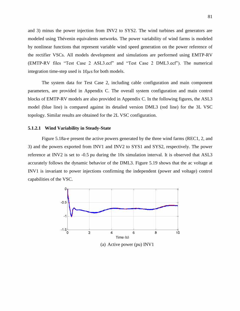
5.1 Dynamic Behavior Validation ........................................................................................ 72
5.1.1 Two- and Three-level AVM VSCs – Test Case 1 ...................................................... 72
5.1.2 Switching Functions Based Models – Test Case 2 .................................................... 80
5.1.3 MMC-based AVM VSCs – Test Case 3 .................................................................... 87
5.1.4 MMC-based STM VSCs – Test Case 4 ..................................................................... 94
5.2 Computing Performance Comparison ............................................................................ 98
5.2.1 AM – Test Case 1 ....................................................................................................... 99
5.2.2 ASL3 – Test Case 2 .................................................................................................. 100
5.2.3 AMM – Test Case 3 ................................................................................................. 100
5.2.4 STM – Test Case 4 ................................................................................................... 100
5.3 Advantages and Limitations of Averaged Models ....................................................... 101
5.3.1 AVM for Two- and Three-level VSCs ..................................................................... 101
5.3.2 AVM Based on Switching Functions ....................................................................... 102
5.3.3 AVM for MMC-based VSCs ................................................................................... 102
5.3.4 Simplified Models for MMC VSCs ......................................................................... 103
5.3.5 Model Suitability for System Studies ....................................................................... 103
CHAPTER 6 CONCLUSIONS ............................................................................................. 105
REFERENCES ............................................................................................................................ 109
APPENDIX A CORRESPONDENCE LIST OF FIGURES AND EMTP-RV FILES ........... 115
APPENDIX B TEST CASE 1 DATA AND EMTP-RV MODELS DESIGN ........................ 118
APPENDIX C TEST CASE 2 DATA AND EMTP-RV MODELS DESIGN ........................ 135
APPENDIX D TEST CASE 3 DATA AND EMTP-RV MODELS DESIGN ........................ 138
APPENDIX E TEST CASE 4 DATA AND EMTP-RV MODELS DESIGN ........................ 152
xi
LIST OF TABLES
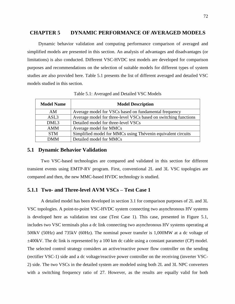
Table 5.1: Averaged and Detailed VSC Models ............................................................................ 72
Table 5.2: AM computing timings for a 3s simulation .................................................................. 99
Table 5.3: ASL3 computing timings for a 3s simulation ............................................................. 100
Table 5.4: AMM computing timings for a 3s simulation ............................................................. 100
Table 5.5: STM Computing timings for a 3s simulation .............................................................. 101
Table 5.6: Summary Table and Comparison of Models .............................................................. 104
xii
LIST OF FIGURES
Figure 2.1: 2L (or 3L) VSC-HVDC terminal ................................................................................... 7
Figure 2.2: MCC VSC-HVDC terminal ........................................................................................... 8
Figure 2.3: 2L Converter topology ................................................................................................... 9
Figure 2.4: 2L Converter voltage (pu) (blue: 50 Hz component, black: converter output) ............. 9
Figure 2.5: 3L NPC converter topology ......................................................................................... 11
Figure 2.6: 3L Converter voltage (pu) (blue: 50Hz component, black: converter output) ............ 11
Figure 2.7: 3L FC converter topology ............................................................................................ 12
Figure 2.8: Generalized topology of a multilevel converter .......................................................... 13
Figure 2.9: Sub-modules a) Two-level cell, b) Full-bridge (H-bridge) cell, c) Half-bridge tree-
level cell ................................................................................................................................. 14
Figure 2.10: Single-phase MMC configuration ............................................................................. 15
Figure 2.11: AC voltage (pu) for a 21-level MMC ........................................................................ 16
Figure 3.1: a) IGBT valve representation, b) Diode V-I curve ...................................................... 22
Figure 3.2: Reference frames: (a) Stationary and (b) rotating 0dq ........................................ 24
Figure 3.3: Phase-locked loop block diagram ................................................................................ 25
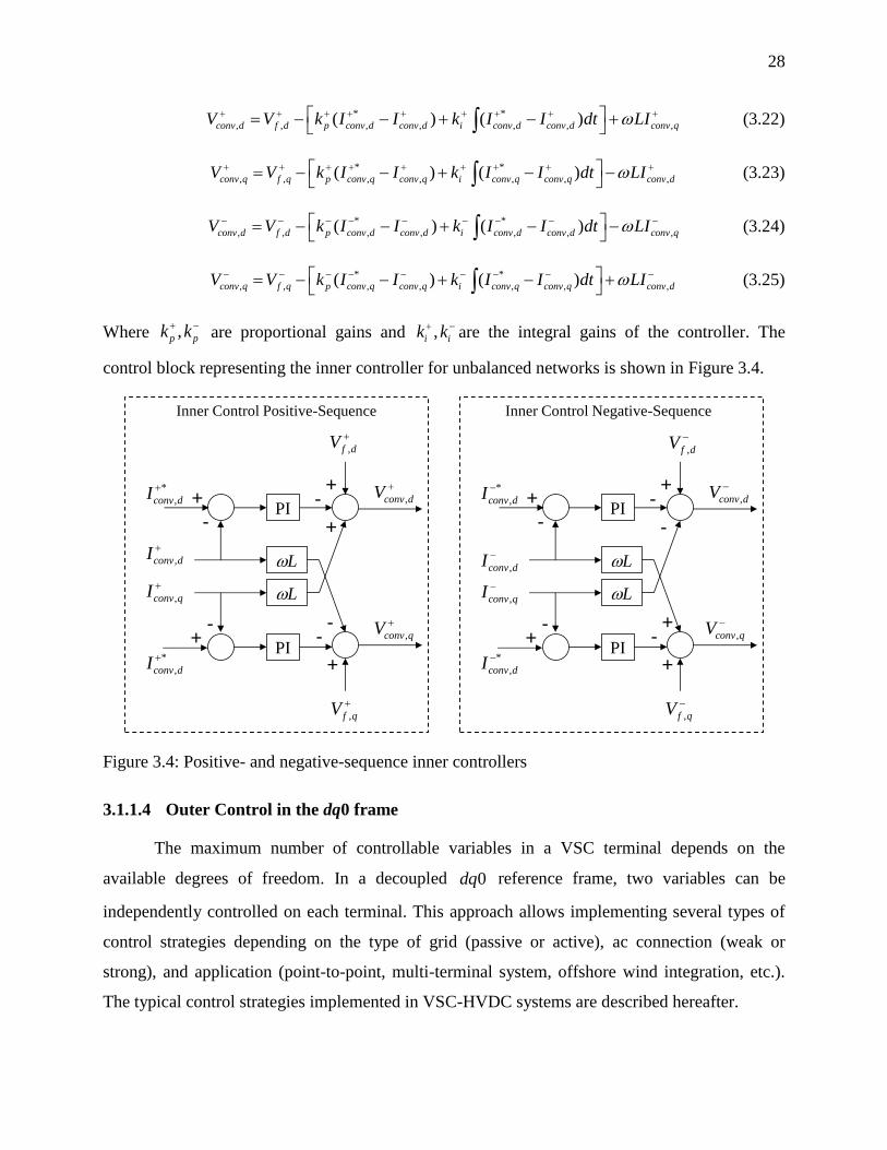
Figure 3.4: Positive- and negative-sequence inner controllers ...................................................... 28
Figure 3.5: Constant voltage and frequency controller .................................................................. 29
Figure 3.6: Active and reactive outer power controller ................................................................. 31
Figure 3.7: Active and reactive current limiter .............................................................................. 31
Figure 3.8: AC voltage controller .................................................................................................. 32
Figure 3.9: DC voltage controller .................................................................................................. 33
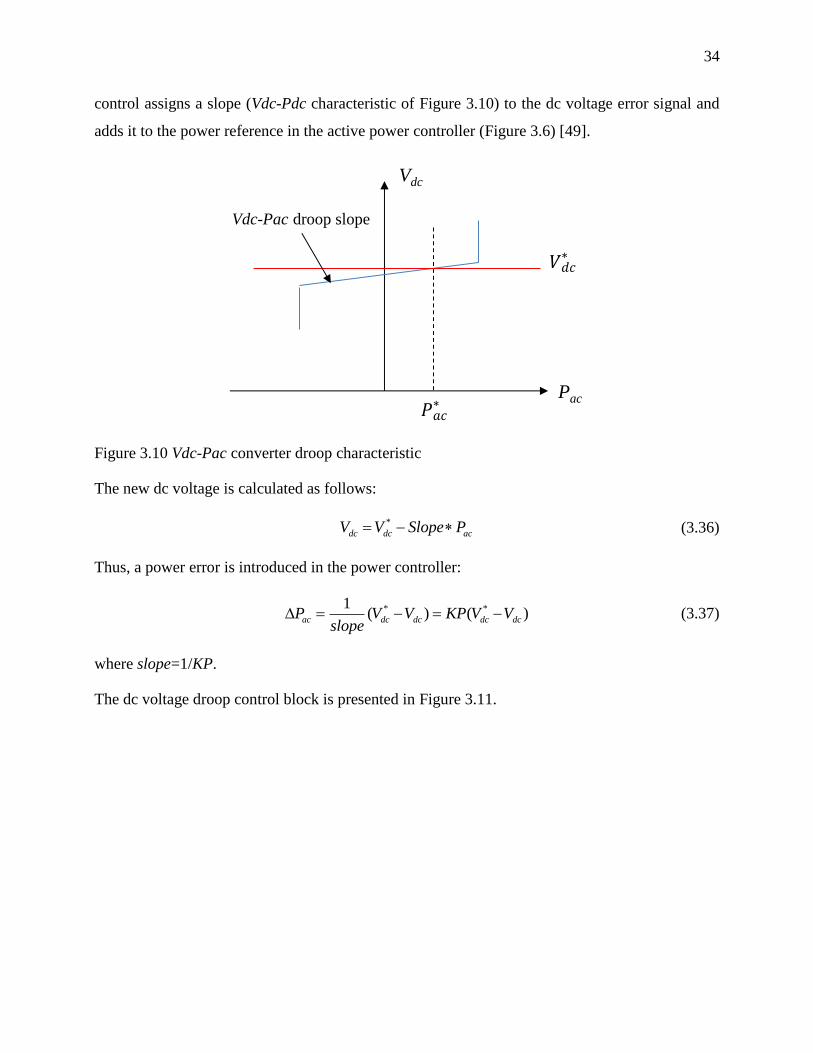
Figure 3.10 Vdc-Pac converter droop characteristic ...................................................................... 34
xiii
Figure 3.11: Active power controller with dc voltage droop control ............................................. 35
Figure 3.12: Active power controller with frequency droop control ............................................. 35
Figure 3.13: Voltage references and PWM triangular carrier waveforms for a 2L VSC .............. 37
Figure 3.14: Voltage references and PWM triangular carrier waveforms for a 3L VSC .............. 37
Figure 3.15: Detailed MMC topology ............................................................................................ 39
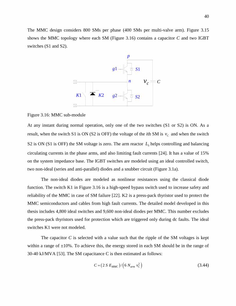
Figure 3.16: MMC sub-module ...................................................................................................... 40
Figure 3.17: BCA procedure .......................................................................................................... 43
Figure 3.18: CCS control block ...................................................................................................... 45
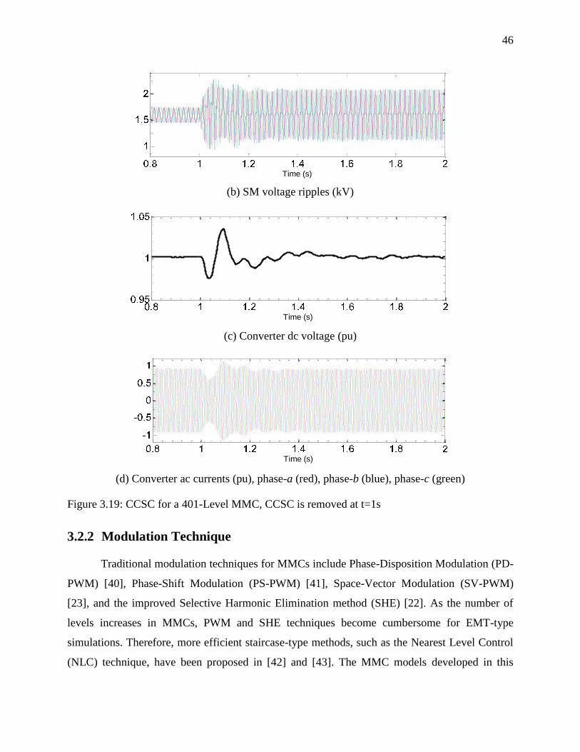
Figure 3.19: CCSC for a 401-Level MMC, CCSC is removed at t=1s .......................................... 46
Figure 3.20: NLC modulation control block .................................................................................. 47
Figure 4.1: Basic switched-inductor and switched-capacitor modules .......................................... 50
Figure 4.2: Current for switched-inductor module during CCM and DCM operation .................. 51
Figure 4.3: Voltage and current waveforms for a 2L VSC ............................................................ 52
Figure 4.4: Voltage and current waveforms for a 3L VSC ............................................................ 52
Figure 4.5: Voltage waveform for 3L VSC during steady-state operation .................................... 53
Figure 4.6: VSC AVM using algebraic parametric functions in the dq0 frame ............................. 55
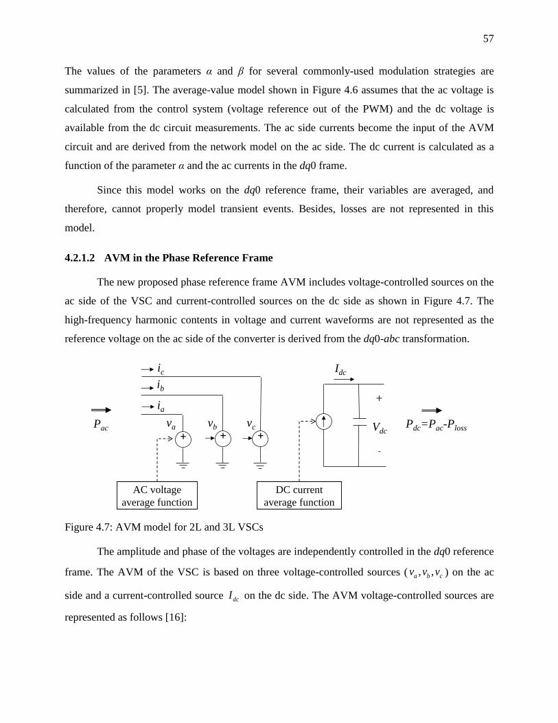
Figure 4.7: AVM model for 2L and 3L VSCs ............................................................................... 57
Figure 4.8: VSC voltage waveforms for 2L and 3L converters ..................................................... 59
Figure 4.9: Switching function circuit model for a 2L VSCs ........................................................ 60
Figure 4.10: 2L converter voltage (pu): DML2 (dashed blue line), ASL2 (solid black line) ........ 61
Figure 4.11: 3L converter voltages (pu): DML3 (dashed blue line), ASL3 (solid black line) ...... 62
Figure 4.12: AC side representation of the AMM ......................................................................... 65
Figure 4.13: AC voltage (pu) for a 21-level AMM ........................................................................ 65
Figure 4.14: DC side representation of the AMM ......................................................................... 66
xiv
Figure 4.15: Equivalent representation of the SM ......................................................................... 68
Figure 4.16: Converter’s multi-valve arm representation of the MMC ......................................... 69
Figure 4.17: SM circuit representation with simplified IGBT model ............................................ 70
Figure 4.18: IGBT Valve: a) Detailed model with non-linear diodes, b) Simplified model ......... 71
Figure 5.1: Test case 1 - VSC-HVDC transmission system using 3L VSCs ................................. 73
Figure 5.2: Active power (pu) VSC-1 with 20% set-point reduction ............................................ 74
Figure 5.3: Active power (pu) VSC-2 with 20% set-point reduction ............................................ 74
Figure 5.4: Reactive power (pu) VSC-2 with 10% set-point reduction ......................................... 74
Figure 5.5: Reactive power (pu) VSC-1 with 10% set-point change on VSC-1 ............................ 75
Figure 5.6: DC voltage (pu) Control VSC-2 with 10% set-point change ...................................... 75
Figure 5.7: AC voltage (pu) VSC-2 with 10% set-point change on VSC-2 .................................. 75
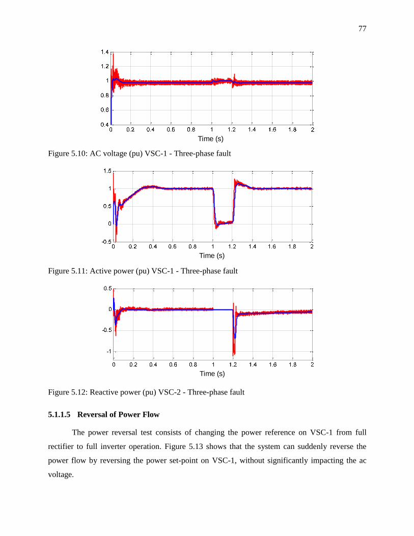
Figure 5.8: DC voltage (pu) VSC-2 - Three-phase fault ................................................................ 76
Figure 5.9: AC voltage (pu) VSC-2 - Three-phase fault ................................................................ 76
Figure 5.10: AC voltage (pu) VSC-1 - Three-phase fault .............................................................. 77
Figure 5.11: Active power (pu) VSC-1 - Three-phase fault .......................................................... 77
Figure 5.12: Reactive power (pu) VSC-2 - Three-phase fault ....................................................... 77
Figure 5.13: Active power (pu) VSC-1 – Power reversal .............................................................. 78
Figure 5.14: AC voltage (pu) VSC-2 – Power reversal ................................................................. 78
Figure 5.15: DC current contribution (A) from VSC-1 - Pole-to-pole fault .................................. 79
Figure 5.16: DC current contribution (A) from VSC-2 - Pole-to-pole fault .................................. 79
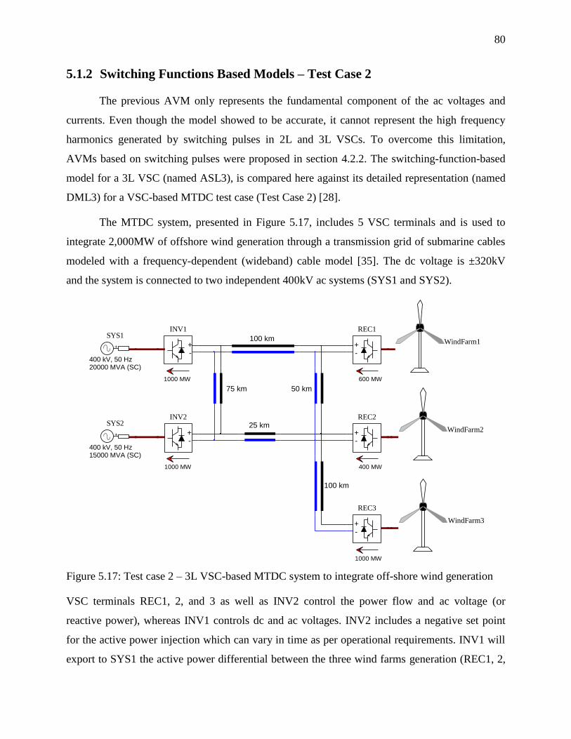
Figure 5.17: Test case 2 – 3L VSC-based MTDC system to integrate off-shore wind generation 80
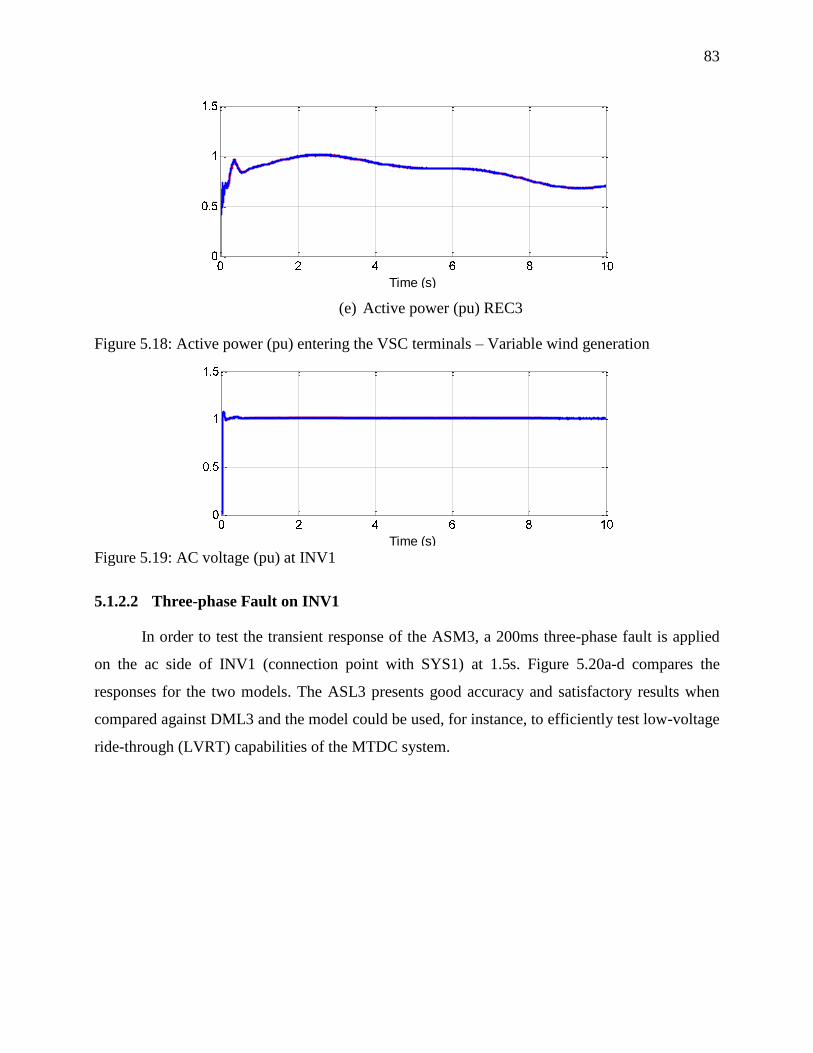
Figure 5.18: Active power (pu) entering the VSC terminals – Variable wind generation ............. 83
Figure 5.19: AC voltage (pu) at INV1 ........................................................................................... 83
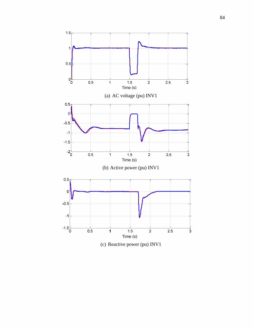
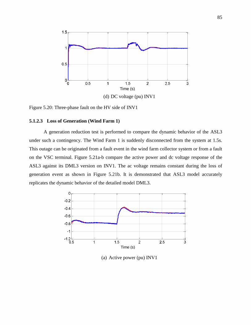
Figure 5.20: Three-phase fault on the HV side of INV1 ................................................................ 85
xv
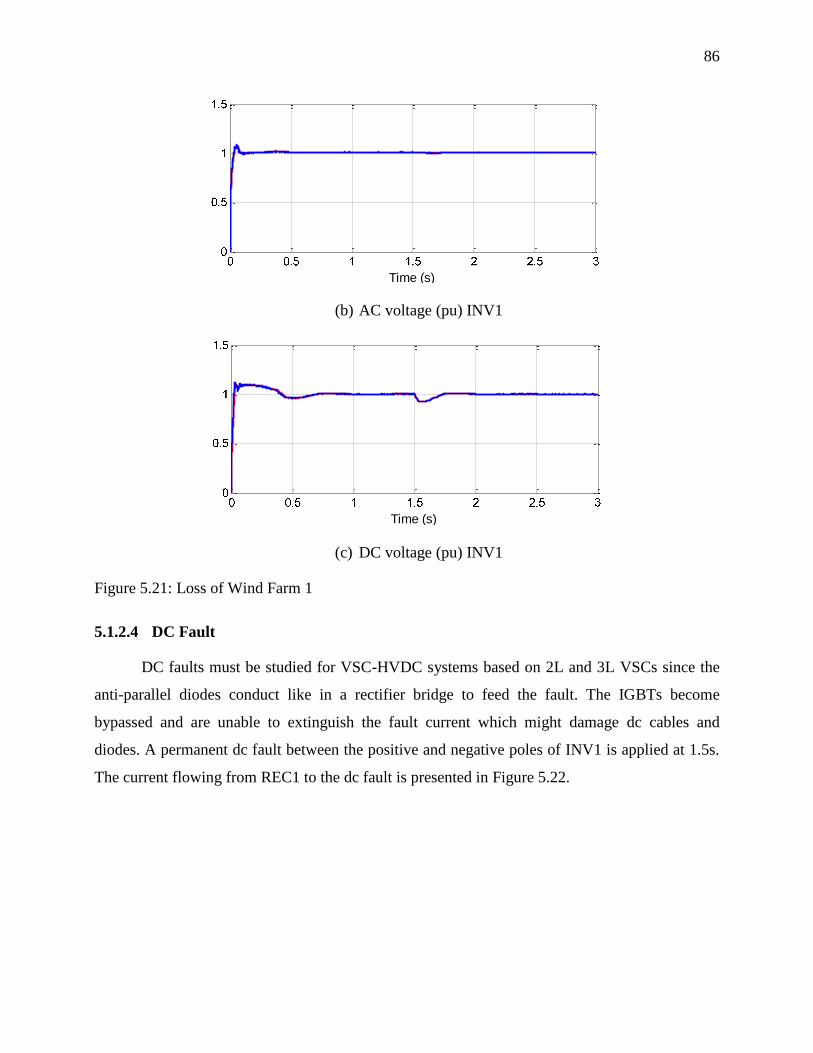
Figure 5.21: Loss of Wind Farm 1 ................................................................................................. 86
Figure 5.22: Current (A) from REC1 - DC Pole-to-pole fault on REC1 ....................................... 87
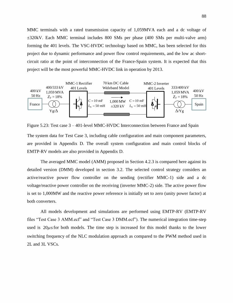
Figure 5.23: Test case 3 – 401-level MMC-HVDC Interconnection between France and Spain .. 88
Figure 5.24: AC voltage sources and switching sequence for initialization .................................. 89
Figure 5.25: Three-phase fault at MMC-2 (Transformer’s HV side) ............................................ 91
Figure 5.26: Active power reversal ................................................................................................ 92
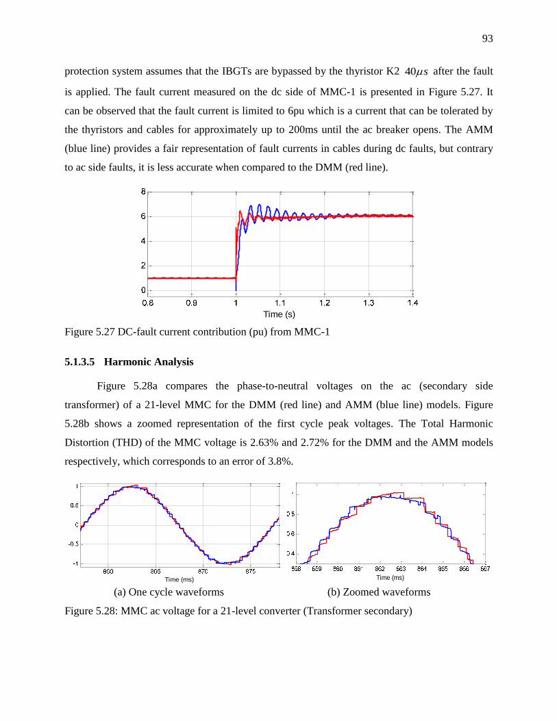
Figure 5.27 DC-fault current contribution (pu) from MMC-1 ....................................................... 93
Figure 5.28: MMC ac voltage for a 21-level converter (Transformer secondary) ......................... 93
Figure 5.29: AC voltages at MMC-1 (pu), phase-a: black, phase-b: blue, phase-c: green ............ 94
Figure 5.30: Test case 4 – 21-level MMC-HVDC Interconnection ............................................... 94
Figure 5.31: Three-phase fault at MMC-2 (Transformer’s HV side) ............................................ 97
Figure 5.32: DC-fault current contribution (pu) from MMC-1 ...................................................... 98
Figure 5.33 MMC ac voltage for a 21-level converter ................................................................... 98
Figure 5.34: AM response to a fault at the inverter side – Simulation time step of 300µs ............ 99
xvi
LIST OF NOTATIONS
(1.1) Equation 1.1
[1] Reference 1
2L Two levels
3L Three levels
xvii
LIST OF ABBREVIATIONS
A Amperes
ac Alternating Current
AVM Average-value Model
BCA Balancing Control Algorithm
CCSC Circulating Current Suppression Control
CP Constant Parameter Model
CSC
dc
Current Source Converter
Direct Current
DLL Dynamic Link Library
DM Detailed Model
DSP Digital Signal Processor
EMT Electromagnetic Transients
EMTP-RV Electromagnetic Transients Program, Restructured Version
FACTS Flexible ac Transmission Systems
FD Frequency Dependent Line Model
GTO Gate Turn-off Thyristor
HV High Voltage
FC Flying Capacitor
HM Hybrid Multilevel
HVDC High Voltage Direct Current
IGBT
kV
Insulated Gate Bipolar Transistor
kilo-Volt
LVRT
LCC
Low-voltage Ride Through
Line Commutated Converter
MMC Modular Multi-level Converter
MTDC Multi-terminal Direct Current
MV Medium Voltage
MVA Mega Volt-Ampere
MVAR Mega Volt-Ampere Reactive
xviii
LIST OF ABBREVIATIONS
MW Mega Watts
NPC Neutral-point Diode-clamped
PI Proportional Integral Control
PLL Phase-locked Loop
POI Point of Interconnection
pu Per Unit
SCL Short-circuit Level
SM Sub-module
TD Time Domain
THD Total Harmonic Distortion
VCO Voltage Controlled Oscillator
VSC Voltage-sourced Converter
WB Wideband Line or Cable Model
xix
LIST OF APPENDICES
APPENDIX A CORRESPONDENCE LIST OF FIGURES AND EMTP-RV FILES ............ 115
APPENDIX B TEST CASE 1 DATA AND EMTP-RV MODELS DESIGN ......................... 118
APPENDIX C TEST CASE 2 DATA AND EMTP-RV MODELS DESIGN ......................... 135
APPENDIX D TEST CASE 3 DATA AND EMTP-RV MODELS DESIGN ......................... 138
APPENDIX E TEST CASE 4 DATA AND EMTP-RV MODELS DESIGN ......................... 152
1
CHAPTER 1 INTRODUCTION
This work presents the development of dynamic averaged models for the accurate and
efficient representation of VSC-based HVDC systems technology in EMT programs. The models
developed are compared against their detailed representation for validation purposes. The
comparison is performed for different VSC-HVDC configurations, converter topologies and
applications. This work also presents a detailed description of different VSC-based technologies
to introduce researchers into this field. All models developed during this work, including
converters topologies, control systems, algorithms, and test cases were developed in the
electromagnetic transient software EMTP-RV [1].
1.1 Motivation
Detailed modeling of HVDC systems include the representation of thousands IGBT
switches and must normally use small numerical integration time-steps to accurately represent
fast switching events. The computational burden introduced by such models highlights the need
to develop simplified models that provide similar dynamic and transient behavior. These
simplified models are known as mean- or average-value models (AVMs) and their objective is to
replicate the average response of switching devices and converters by using simplified functions
and controlled sources [2]-[5]. A different AVM concept is the switching function which intends
to mimic the high frequency pattern of VSCs allowing the representation of high frequency
harmonics [6]-[8]. AVMs have been successfully developed for low power applications in the
aerospace and aircraft industry [9], [10] and for wind generation technologies [11]-[13].
However, it is a new trend in high power systems with few applications presented to date
including traditional two and three-level VSC-HVDC models in EMT programs [14]-[16].
Reference [17] develops an efficient methodology for simulating MMC systems in EMT-type
programs, but it does not model a detailed MMC including a large number of levels and
integrated into a large scale transmission system.
The development of accurate and efficient averaged models in EMT programs enables the
use of VSC-HVDC technologies integrated into a large grid which corresponds to the main
motivation of this research work.
2
1.2 Contributions of the Thesis
The main objective of this thesis is to overcome the existing computing limitations
associated with the detailed modeling of VSC-based HVDC system integrated to large grids. This
thesis contributes to the comparison of existing models as well as the development of new
averaged models for different VSC technologies. The proposed models are computationally
efficient and accurate for the modeling of dynamic and transient events in power systems. The
main contributions of this thesis include:
Providing a comprehensive literature review and description of the available VSC-based
HVDC technologies, their main component, applications, and comparison with
conventional LCC-based HVDC technologies.
Providing comprehensive review and description of the available averaging modeling
techniques and methods currently used in power electronic applications as well as
exploring their applicability to VSC-based HVDC technologies.
Developing detailed two- and three-level VSC-based HVDC models for different
applications in EMTP-RV. These models include converter’s IGBT switches, control and
protection systems. They are built with the purpose of validating the proposed averaged
models.
Developing detailed MMC-based HVDC models for different applications in EMTP-RV.
The models include converter’s IGBT switches, control and protection systems. They are
built with the purpose of validating the proposed averaged models. These detailed MMC-
based models are the first and only full model benchmark available for model validation
and for the use in the studies where averaged models may not be suitable.
Developing efficient averaged models for different VSC-HVDC systems that accurately
represent the dynamic and transient behavior of this technology when integrated into large
grids. Identifying advantages and limitations of the developed models and their suitability
to represent different events in power systems.
Building test cases in EMTP-RV to demonstrate accuracy and performance of the
developed models. Test cases include applications such as point-to-point HVDC
3
terminals, asynchronous HVDC interconnections, and MTDC systems to integrate
offshore wind generation.
Comparing different VSC-based technologies and assessing their impact on harmonic
content, controllability and fault ride-trough capabilities.
Identifying advantages and limitations of the developed averaged models and studying
their suitability to model different events in power systems.
1.3 Methodology
The methodology proposed involves developing detailed models (DMs) in EMTP-RV that
accurately represent the actual behavior of VSC-HVDC technologies. These DMs are used to
validate the proposed AVMs for different test cases and scenarios. The validation criteria
involves comparing systems response to different disturbances such as ac faults, dc faults,
changes on power and voltage order set points, power inversion test and other dynamic and
transient tests. An initialization technique is proposed to properly set the initial conditions for the
time-domain simulation from the multiphase load-flow module of EMTP-RV. The model
validation includes the comparison of different variables in time-domain and the comparison of
the harmonic content of voltages and currents. The simulation times for different time-steps will
be used as a parameter to compare the computing performance and efficiency of the proposed
models.
1.4 Thesis Outline
The work presented in this thesis is divided into the following chapters:
Chapter 1: Introduction.
Chapter 2: VSC-HVDC Technology: Describes the existing VSC-based HVDC
technologies, main components and applications.
Chapter 3: Detailed VSC-HVDC Models: Develops detailed models for VSC-based
technologies to be used in the validation of the proposed AVMs.
Chapter 4: Average-value Models for VSC-HVDC Systems: Presents the available
methodologies for averaging of power converters used in HV and LV applications, and
4
develops new averaged models for different VSC-based technologies applied to HVDC
transmission. It also presents available simplified methods for efficient modeling of VSC-
HVDC systems.
Chapter 5: Dynamic Performance of Averaged Models: Performs a comparison and
validation of the averaged models developed against their detailed representation for
different VSC-HVDC applications. It also presents the advantages and limitations of the
proposed models.
Chapter 6: Conclusions.
The thesis is complemented with appendices (B to E) that include all relevant data required
to replicate the proposed models and test cases as well as block diagrams showing the models
design developed in EMTP-RV. Appendix A provides a summary list with the correspondence
between the figures in this thesis and their respective EMTP-RV files (test cases).
5
CHAPTER 2 VSC-HVDC TECHNOLOGY
This chapter starts with a brief introduction to HVDC systems followed by a description of
the currently available VSC technologies applied to HVDC transmission including main system
components, converter topologies, modulation techniques, and control and protection systems.
2.1 Technology Background
Three-phase alternating current (ac) has been the dominant solution for high-power long-
distance transmission since the 19th century. The highest commercial voltage level, initially
adopted in 1968, is 765kV. Even though few facilities have been built and are operated at higher
voltages (1,000kV and 1,200kV), 765kV remains as the highest commercial transmission voltage
currently in operation. In ac transmission systems however, the maximum transfer capability may
be limited by not only thermal, but also stability and reliability constraints. In order to increase
transfer capability, reduce losses and improve stability margins in long transmission lines, series
and shunt compensation may be required forcing the use of costly switching substations or
building parallel lines. Transfer capability limitations are particularly true for ac transmission
involving underground (or submarine) cables where shunt compensation is required causing
stability problems in some cases [18].
The development of HVDC transmission technology in 1954 introduced a bright
opportunity for long distance transmission due to its superb capabilities and advantages in
comparison to ac technologies. Some of the advantages of traditional HVDC over ac transmission
are the reduced line losses and cost for comparable distance and capacity. It enables the use of
HV cable connections and asynchronous interconnections, and also allows controllability of
power flows and voltage which helps improving system stability. Other advantages are the
isolation from disturbances of two interconnected systems and the limitation of fault currents and
short-circuit levels.
Early development of power electronics for HVDC technologies back in 1939 considered
the use of Current Source Converters (CSC) based on mercury-arc valves as it was found to be
the most suitable technology to handle large currents. The appearance of the thyristor
semiconductor in 1950 had an enormous impact on static-converter technology and it started to
6
be used in HVDC transmission by mid-1970s. Ever since, LCC technology based on thyristor
valves has dominated the HVDC industry.
From 1990 onwards, the VSC technology became economically viable thanks to the
development of self-commutated high-power switches, such as GTOs and IGBTs, and the
computing power of Digital Signal Processors (DSPs) to generate the firing patterns. HVDC
markets involving long-distance high-power transmission are still dominated by traditional
thyristor-based HVDC technology, but it is expected that VSC-based technology will replace
traditional CSC technology in future due to the fast development of high-power semiconductor,
controls systems and protection schemes [19].
VSC-HVDC systems have the capability to rapidly control both active and reactive power
independently of each other to keep the voltage and frequency stable. This gives total flexibility
regarding the location of the power converters in the system including ac networks having a very
low Short-circuit Level (SCL). In contrast to LCC technology, the polarity of the dc link voltage
remains the same with the dc current being reversed to change the direction of power flow which
eliminates the issue of commutation failures. In addition, VSC-HVDC systems enable black start
and emergency support, stabilization of ac grids, fast reverse power flow control, multi-terminal
dc implementation, and eliminate the need of ac filters and the use of grounding electrodes due to
bipolar operation [20].
Different VSC topologies have been developed in the past 20 years. However, only two
have been successfully implemented in HVDC applications: two-level (2L) and multilevel
neutral-point diode-clamped (NPC), also known as three-level (3L) [20], [21]. Recent trends on
multilevel converters for HVDC include modular multilevel converter (MMC) topology which
connects 2L converter modules in cascade to achieve the desired ac voltage [22]-[24]. VSC-
HVDC technologies are currently offered by three manufacturers ABB [25], Siemens [26] and
Alstom Grid [27].
2.2 VSC-HVDC System Overview
Figure 2.1 shows a high-level representation of a VSC-HVDC terminal for 2L (or 3L)
converter topology. A three-phase transformer, with its secondary winding connected in delta to
block the zero-sequence voltages generated by the VSC, is used to interface the converter with
7
the ac system. A series reactor (L) is added between the converter and the transformer for control
of active and reactive powers and low-pass filtering of the PWM pattern. It is also used to limit
the short-circuit currents. The primary objective of the dc side capacitor (C) is to provide a low
impedance path for the turned-off current, to reduce harmonic ripple on the dc voltage (filter) and
also to serve as an energy storage device. The control system uses a vector-type control that
includes a Phase Locked-loop (PLL), an outer controller and an inner controller. VSCs based on
2L and 3L topologies typically use high-frequency (greater than 1,000Hz) PWM or space-vector
modulation [28], [29].
Figure 2.1: 2L (or 3L) VSC-HVDC terminal
New VSC technologies are based on multilevel configurations where 2L sub-modules
(SMs) are connected in cascade to form a MMC. The overall configuration of a MMC terminal is
presented in Figure 2.2. MMC topologies use a smaller switching frequency helping to reduce
converter losses. In addition, filter requirements are eliminated by using a significant number of
levels per phase. Scalability to higher voltages is easily achieved and reliability improved by
increasing the number of SMs per multivalve arm [30]. The dc capacitors are now included in
each SM and the series reactors, used to control the power flow and circulating currents, are
Idc
S
VSC DC Cable
Yg/∆
L C
PWM
Inner
Current
Control
Outer P/Q/Vdc
Control
PLL
Ѳ
Ѳ
+
Vdc
-
abc
sv abc
fv
abc
convi
abc
convv
8
embedded in the converter’s phase arms. A Balancing Control Algorithm (BCA) is required to
control arm currents and the dc voltage on each SM capacitor [40].
Figure 2.2: MCC VSC-HVDC terminal
2.3 VSC Topologies
VSCs are based on state-of-the-art IGBT semiconductor switches with turn-on/turn-off
capabilities and operate at high or low frequencies depending on the topology and modulation
technique. The focus of this thesis covers 2L, 3L-NPC and MMC topologies. Other multilevel
topologies used in HV and MV applications, such as Flexible ac Transmission Systems
(FACTS), are also discussed in this section.
2.3.1 Two-level Converter
The 2L topology has been used in a wide range of power levels including VSC-HVDC
transmission. The basic configuration of a three-phase 2L converter is presented in Figure 2.3.
Actual systems use packs units grouping several IGBTs switches in series each capable of
handling currents between 1-2kA and voltages up to approximately 3kVdc [25]. Features taken
into account when designing and specifying IGBT switches are high blocking voltage and turn-
off current, low conduction and switching losses, short turn-on and turn-off times, suitable for
S MMC
VSC DC Cable
Yg/∆
Modulation
& BCA
Inner
Current
Control
Outer
P/Q/Vdc
Control
PLL
Ѳ
Ѳ
Idc
+
Vdc
-
abc
sv abc
convv
abc
convi
9
series connection, high /dv dt and /di dt withstand capability, good thermal characteristics, and
low failure rates [21].
Figure 2.3: 2L Converter topology
The voltage pattern generated by a 2L converter oscillates between +Vpos and -Vneg (two
voltage levels) at a predefined switching frequency. Figure 2.4 shows the 2L converter output and
the dominant 50Hz component for a switching frequency ratio of 27 (1,350Hz). The sinusoidal
carrier-based PWM produces a voltage waveform with a dominant component plus significant
high-order harmonics which are eliminated by means of tuned filter and high-order damped
filters.
Figure 2.4: 2L Converter voltage (pu) (blue: 50 Hz component, black: converter output)
+Vpos
-Vneg
Va
Vb
Vc
S1 S3 S5
S2 S4 S6
++
Time (ms)
10
Although a VSC feeds fundamental ac current into the system, the converter voltage output is in
reality a rectangular waveform. The ac system components connected to the VSC would be
exposed to very large step changes in voltage with /dv dt levels up to l00kV/µs. This waveform
is unacceptable for direct connection to an ac networks and, if a converter transformer is
employed, high-frequency filters are generally used to limit the transformer’s exposure to high
/dv dt levels. The advantages of the 2L topology are simpley circuitry, small dc capacitors and
footprint, and the same duty is required for all the IGBTs. The main disadvantages are the large
blocking voltage required for the IGBTs, crude waveforms forcing the need of filters and high
converter losses due to the high switching frequency [21].
2.3.2 Multilevel Converters
Several multilevel converter topologies have been developed in the past for different HV
and MV applications. Most typical multilevel configurations are diode-clamped (NPC), flying
capacitor (FC) and hybrid multilevel (HM) converters [31]-[33]. Each configuration may contain
several levels, but three-levels have been used in HVDC applications and particularly the NPC
topology. A brief description of each of them is provided in this section with emphasis in 3L-
NPC topology.
2.3.2.1 Neutral Point Diode-clamped Converter
The configuration of a three-phase 3L-NPC converter is presented in Figure 2.5. The
voltage pattern generated by a 3L converter has three levels 0, +Vpos and -Vneg oscillating at the
switching frequency. Taking phase a in Figure 2.5, when IGBTs S11 and S12 are turned ON, the
output is connected to +Vpos and when S12 and S21 are ON, the output is connected to ground.
When S21 and S22 are ON, the output is connected to -Vneg. Clamp diodes provide the
connection to the neutral point (or ground). From the switching states, it can be deduced that
IGBTs S12 and S21 are ON for most of the cycle, resulting in greater conduction loss than S11
and S22, but less switching loss. The dc bus capacitors are connected in series and establish the
mid-point neutral voltage (ground in the case of Figure 2.5). In NPC inverters, maintaining the
voltage balance between the capacitors is important for the proper operation of the NPC
topology.
11
Figure 2.5: 3L NPC converter topology
Figure 2.6 shows the 3L converter output and the dominant 50 Hz component for a switching
frequency ratio of 27 (1,350Hz). Similar to the 2L topology, PWM produces a voltage waveform
with a fundamental component plus high-order harmonics which are eliminated by means of
tuned and high-order damped filters.
Figure 2.6: 3L Converter voltage (pu) (blue: 50Hz component, black: converter output)
The switching sequence required to generate the voltage pattern is described in reference [31].
The advantages of the 3L-NPC topology are reasonably small dc capacitors needed, lower switch
-Vneg
Va
+Vpos
Vb
Vc
S11
S12
S21
S22
S31
S32
S41
S42
S51
S52
S61
S62
++
Time (ms)
12
blocking voltages, small footprint, improved basic ac waveform and relatively low converter
switching losses. Among the disadvantages is the inherent difficulty in keeping dc capacitor
voltages constant, complex circuitry for large number of levels, the number of added diodes
increases rapidly with the number of levels and semiconductor switches have different duties
[21].
2.3.2.2 Flying Capacitor Converter
The configuration of a three-phase 3L FC converter is presented in Figure 2.7. Similar to
the 3L NPC converter, the voltage pattern generated by a 3L FC converter has three levels 0,
+Vpos and -Vneg oscillating at the switching frequency. The switching sequence required to
generate the voltage pattern is also described in reference [31].
Figure 2.7: 3L FC converter topology
This topology has no additional diodes, but has additional dc capacitors known as floating
(or flying) capacitors. For a three-phase unit, the main dc capacitors are shared by the three
phases, but the FC are equal but independent for each phase and are connected to the mid-point
connection of the upper and lower diodes on each phase leg. During normal operation, the mean
-Vneg
Va
+Vpos
Vb
Vc
S11
S12
S21
S22
S31
S32
S41
S42
S51
S52
S61
S62
FC FC FC
++
+ + +
13
voltages of the FCs for each phase are charged at +Vpos, where the voltage of the main dc bus
voltage is Vdc (Vpos+Vneg). As a result, the voltage across each IGBT switch is only half of the
dc-link voltage Vdc. Taking phase a in Figure 2.7, when IGBTs S11 and S12 are turned ON, the
output is connected to +Vpos and when S11 and S21 are ON, the output is zero (-Vpos+Vpos).
When S21 and S22 are ON, the output is connected to -Vneg. States S11 ON and S22 ON, as well
as S12 and S21 ON, are forbidden to avoid shorten the capacitors.
The advantages of the 3L FC topology are similar to the 3L NPC with the difference that all
switches have the same duty. With the volume of capacitors largely proportional to the square of
their nominal voltages, the disadvantage of this topology is the large footprint incurred by the
floating capacitors [21].
2.3.2.3 Hybrid Multilevel Configurations
The generalized structure of a single-phase multilevel inverter with n m-level SMs (or cells)
connected in series is shown in Figure 2.8.
Figure 2.8: Generalized topology of a multilevel converter
m-level
cell
m-level
cell
m-level
cell
m-level
cell
V1
V2
V3
Vn
Vdc1
Vdc2
Vdc3
Vdcn
14
A phase-to-neutral voltage waveform is obtained by adding up the output voltages of each
cell nV . It is considered that the output voltage of each cell represents equally spaced levels,
where the voltage step between two adjacent levels is a function of nVdc . Several topologies of
single-phase cells, such as those presented in Figure 2.9, can be connected in series (or cascade)
to obtain multilevel waveforms. Full-bridge cells (Figure 2.9b) are usually employed in FATCS
devices (STATCOM) because they use a smaller dc bus voltage level, and they present a smaller
number of components than half-bridge cells with the same number of levels. On the other hand,
full-bridge cells cannot synthesize voltage waveforms with an even number of levels. Although
each configuration has its advantages and disadvantages, the unified analysis presented
hereinafter does not depend on the arrangement adopted to obtain a given number of levels [32].
A hybrid configuration will combine different level cells in series or different modulation
techniques. A multilevel configuration currently used for VSC-HVDC connects two-level cells
(Figure 2.9a) in series to form the desired ac voltage configuration and is known as modular
multilevel converters (MMC) [23]. As opposed to full-bridge cells, which can generate three Vi
voltage levels (+Vdc, 0 and –Vdc), half-bridge cells can only generate two levels (+Vdc and –Vdc,
or +Vdc and 0). Half-bridge tree-level cells (Figure 2.9c) can also produce three levels, but they
require additional diodes (clamp diodes) which make this topology more onerous for multi-level
converter applications.
(a) (b) (c)
Figure 2.9: Sub-modules a) Two-level cell, b) Full-bridge (H-bridge) cell, c) Half-bridge tree-
level cell
+
Vi
-
+
Vi
-
+
Vi
-
+
+
+
+
15
2.3.3 Modular Multilevel Converters
The MMC topology is a new configuration developed for VSC-based HVDC applications.
It connects two-level SMs in series to generate the ac voltage output. Figure 2.10 shows a single-
phase MMC configuration including Nu SMs on the upper arm and Nl SMs on the lower arm.
Each SM contains two IGBT switches and a capacitor.
Figure 2.10: Single-phase MMC configuration
Regardless of the sign of the arm current, the voltage smv of each SM can be switched to either 0
or to the capacitor voltage cv . By switching a number of SMs in the upper and lower arms, the
voltages dcV and av are controlled. The voltage on the capacitors are periodically measured with
a typical sampling-rate in the millisecond-range and, according to their voltage value, they are
sorted by software. In case of positive arm current (entering into the SM), the required number of
SMs with the lowest voltages are switched on (S1=ON, and S2=OFF) and the selected capacitors
are charged. When the current in the corresponding arm is negative (going out of the SM), the
SM-1
SM-2
SM-Nu
:
SM-1
SM-2
SM-Nl
:
Ls/2
ia
va
Ls/2Sub-Module
C
S1
S2vsm
+
-
+
-
vc
Vdc
Idc
Multi-valve
Arm
16
number of SMs with highest voltages are switched on. By using this method, continuous
balancing of the capacitor voltages is guaranteed. The MMC configuration typically includes
redundant SMs, meaning a defective SM can be replaced by a redundant SM in the arm by
control action without mechanical switching. This results in an increased safety and availability
for this configuration [34].
The converter reactor SL has two key functions:
Three-phase MMCs connect the multi-valve arms in parallel on the dc side. As the
generated dc voltages on each arm cannot be exactly the same, balancing currents will
appear between the individual phase arms. The converter reactors help damping these
balancing currents to a very low level and make them controllable by means of
appropriate methods.
The reactors substantially reduce the effects of faults arising inside or outside the
converter. As a result, unlike in previous 2L and 3L VSC topologies, current rise rates of
only a few tens of amperes per microsecond are encountered even during critical faults
such as a short circuit between the dc terminals of the converter. These faults are swiftly
detected and, due to the low current rise rates, the IGBTs can be turned off at absolutely
uncritical current levels.
The voltage pattern generated by a MMC is a staircase waveform where each step corresponds
the SM voltage (or capacitor voltage) cv . Figure 2.11 shows the ac voltage waveform for a
detailed 21-level MMC (20 SMs per multi-valve arm).
Figure 2.11: AC voltage (pu) for a 21-level MMC
Time (s)
17
It can be noted that the higher the number of SMs, the lower the harmonic content and the need
for filtering. An actual MMC-based HVDC systems of 400MW will include 200 SMs per multi-
valve arm on each phase. A larger system in the range of 1,000MW will contain 400 SMs per
multi-valve arm forming what is known as a 401-level MMC. These large systems will not
require any filter on the ac side of the converter as the voltage output will be almost a perfect
sinusoidal waveform as it will be demonstrated later on. The typical dc voltage for an actual 201-
and 401-level MMC is 200kV and 320kV, respectively [30], [34].
A detailed description of a three-phase MMC topology and its control system is provided in
section 3.2 of this thesis.
2.4 Filtering Requirements
VSCs based on two- and three-level topologies are usually operated using sinusoidal PWM
technique to control the fundamental frequency and the modulation index of the ac voltage. As
previously shown in Figure 2.4 and Figure 2.6, the converter’s voltage output includes a
fundamental frequency plus high frequency components. Elimination of harmonics in VSCs is
achieved by the use of ac filters. The series reactor will also help to filter the harmonic content. A
typical VSC-HVDC scheme will include a couple of tuned filters plus a high frequency filter.
The filters are tuned at the switching frequency and twice the switching frequency. The
transformer connection is delta on the secondary side (converter side) in order to remove third-
order harmonics. Depending on the filter performance requirements, the filters size will vary
between 10-30% of the rated converter’s capacity [20]. The requirements for 2L and 3L VSC
filter are as follows:
1
1.0%hh
UD
U (2.1)
2 1.5% 2.5%,h
h
THD D (2.2)
where hD is the individual voltage harmonic distortion and THD is the Total Harmonic
Distortion measured at the Point of Interconnection of the VSC-HVDC system. These are voltage
quality performance measures. There is also a telephone influence factor (TIF) that is used as an
indication of the expected telephone interference. Filters are also added on the dc side along with
18
smoothing reactors where the converter capacitor is installed in order to suppress harmonics.
Cables on the dc side may run close to telephone lines causing interference, therefore, additional
filtering may be required to minimize telephone interference from dc cables.
The high /dv dt in the switching valves may cause a high frequency noise which should be
prevented from propagation to the rest of the system and outside the converter facilities.
Mitigations measures are implemented at the valve level by using dumping circuits, but radio
interference (RI) filter capacitors and reactors connected between the ac bus and earth are
typically used.
MMC-based VSC-HVDC systems using a large number of levels (above 100) do not
require ac filters to improve voltage quality as the converter output will be an almost perfect
sinusoidal waveform. Harmonic content analyses for different converter levels will be studied in
a further section of this report.
2.5 DC Link
The dc link in 2L and 3L VSCs is formed by the storage capacitors and the dc cable or
overhead line, respectively. The primary objective of the dc side capacitor is to provide a low-
inductance path for the turned-off currents and also to serve as an energy storage device. The
capacitor also reduces the harmonics ripple on the direct voltage. Disturbances in the system (e.g.
ac faults) will cause dc voltage variations. The ability to limit these voltage variations depends on
the size of the dc side capacitor. A storage capacitor provides the corresponding VSC with a
smooth dc voltage of a fixed polarity. To achieve maximum use of the power semiconductors of
the VSC, the capacitor needs to be connected to the converter by a low inductive path. The size
of the capacity is chosen according to the maximum dc voltage ripple tolerated [20]. It should be
noted that a dc capacitor is not required in MMC configurations as the storage capacitor is now
embedded in the converter’s SM. This particularity will reduce the stress on the IGBT switches
due to /dv dt variations.
A VSC-HVDC system cannot change voltage polarity. Power reversal is achieved by
changing the direction of dc current instead. This enables the use of extruded dc cables, which are
an attractive alternative to self-contained oil filled or mass impregnated paper insulated cables as
used for conventional thyristor-based HVDC systems. The cable length is not limited as it would
19
be in case of ac transmission systems. VSC-HVDC systems use land or submarine polymer
cables similar to XLPE ac cables, but with a modified polymeric insulation. Cable data for dc
cables can be found in [20].
For the purpose of this thesis, the dc cables used in EMTP-RV are modeled using a
wideband frequency dependent cable model [35] in order to study both dynamic and transient
events on the dc side of the VSC-HVDC link.
2.6 Control System
A high level overview of the control system for a 2L (or 3L) and a MMC-based VSC was
presented in section 2.2. The basic control scheme uses a vector control (Figure 2.1) which
includes an outer controller that generates the current references in the 0dq synchronous rotating
frame to the inner controller [36], [37]. The purpose of the inner current controller (or ac current
controller) is to allow the (active and reactive) current through the series reactor and the
transformer to be controlled. The synchronous frame rotates at the frequency obtained from the
PLL which synchronizes the converters voltage with the ac voltage. The inputs to the PLL are the
ac voltages of the three-phases at the Point of Interconnection (POI). The current references to
the inner controller are obtained from the outer controller (or current-order controller) whose
inputs are the active and reactive reference power, or the rms voltage on the converter filter. The
dc voltage is also controlled through the outer controller by a current reference order. A voltage-
dependent current order limiter provides control to keep the ac filter voltage within its upper and
lower limits. The tap changer of the converter transformer is controlled to keep the voltage
modulation ratio ( vm ) within acceptable limits. The frequency can be controlled in cases where
VSC-HVDC system is supplying a passive (no sources or active elements) network [38]. The
reactive power control includes an ac voltage override block intended to maintain the ac voltage
within acceptable pre-defined limits. The active power control, in turn, includes a dc voltage
limiter that overrides the active power control in order to maintain the dc voltage within an
acceptable range.
Multilevel (three levels or higher) converters present the problem of having the neutral-
point voltage subject to fluctuations due to the irregular charging and discharging cycle of the
upper and lower dc capacitors. This unbalance may cause excessive overvoltages on the
20
switching devices and on the dc capacitors. The dc-voltage regulation method used in this thesis
controls the zero-sequence current and adds a zero-sequence signal to the voltage reference of the
PWM [39]. MMCs on the other hand, need to balance the second-harmonic circulating currents
generated by unbalances in the phase arms as well as the dc capacitor voltage at each SM. This is
achieved by using a circulating current suppression control (CCSC) and a balancing control
algorithm (BCA), respectively [30]. More details on the origin and mitigation of voltage and
current unbalances generated in MMCs are provided in sections 3.2.1.1 and 3.2.1.2, respectively.
Under unbalanced network conditions or grid disturbances, voltage ripple is introduced into
the dc link. To mitigate this effect, a control strategy that decouples positive and negative
sequence inner-current loops can be implemented. This control strategy improves the dynamic
response of the VSC-HVDC system as shown in [44]. The following chapter provides a more
detailed description of the control system developed and used in this thesis for different VSC
topologies.
2.7 Protection System
The main purpose of the protection system is to promptly remove the VSC components
from service in the event of a fault. The main protection device in a VSC-HVDC system is the ac
breaker which disconnects the converter and transformer from the grid removing dc current and
voltage. Depending on the type of fault and converter technology, the clearing actions may go
from transient currents limitation by temporary blocking the valves and control pulses to
permanent blocking of the VSC and ac breaker tripping. The transient current limiter stops
sending pulses to the IGBTs of the faulted phase or all three phases when overvoltage protection
is enabled and is re-established once the fault is cleared. A permanent blocking, whereas, will
send a turn-off signal to all the IGBT switches and they will stop conducting.
VSC-HVDC systems based on MMC technology include, in addition to the ac breaker, a
press-pack thyristor on each SM in parallel to 2S (Figure 2.10) which is used to protect the anti-
parallel diodes exposed to high currents from dc faults. Once a dc fault is detected and the IGBTs
are blocked, the fast-recovery free-wheeling diodes, which have low surge current withstand
capability, are exposed to damaging currents for a few cycles. The thyristor is fired during the
fault allowing most of the current to flow through the thyristors and not through the diodes until
the ac breaker opens [24]. Press-pack thyristors have a high capability to withstand surge currents
21
which make them useful in conventional LCC-HVDC applications and their use in VSC-HVDC
applications will make this technology suitable for applications involving overhead transmission
lines.
2.8 VSC-HVDC Applications
VSC-HVDC systems have the advantage of independently controlling active and reactive
power and voltage which make this technology suitable for a number of applications including
grid performance and operations support. Examples of applications include parallel
interconnection of ac and dc systems where VSC-HVDC link can help damping oscillations in
the ac systems [20]. The advantage of this technology for system restoration is considerable in
terms of voltage and frequency stability during black start. VSC-HVDC will enable applications
requiring asynchronous connections between two systems either back-to-back or by means of dc
transmission links. This advantage increases when the connection requires the use of
underground or submarine cables such as in VSC-based MTDC systems used to integrate
offshore wind generation [45]-[48]. Future in-feed to dense urban cities are an attractive
application of VSC-HVDC systems due to their capability to use cable systems and also to
control voltage and frequency at the VSCs [38].
22
CHAPTER 3 DETAILED VSC-HVDC MODELS
This chapter describes the detailed VSC-HVDC models (and mathematical formulation)
developed in EMTP-RV for the validation of the proposed AVMs. It starts with the first
generation of VSC technologies based on 2L and 3L converters to continue with the latest
generation based on MMC technology.
3.1 Two- and Three-level Converter Models
In the detailed two- and three-level converter topologies, described in sections 2.3.1 and
2.3.2, the IGBT switches are modeled using an ideal controlled switch, two non-ideal (series and
anti-parallel) diodes and a snubber circuit, as shown in Figure 3.1a. The non-ideal diodes are
modeled with nonlinear resistances using the classical V-I curve of a diode whose characteristic
can be adjusted according to manufacturer data (Figure 3.1b). This model offers several
advantages as it can accurately replicate the nonlinear behavior of switching events accounting
for both switching and conduction losses. Six and twelve IGBT valves were modeled for the two-
and three-level converters, respectively. Therefore, the RLC snubber circuit must be calibrated to
account for losses in the case of an actual VSC system where several IGBTs are connected in
series and parallel in order to withstand the design voltage and current.
(a) (b)
Figure 3.1: a) IGBT valve representation, b) Diode V-I curve
It should be noted that partial differential equations could be used to develop a lumped circuit for
the IGBT valve. In [61], a complex IGBT sub-circuit is proposed and compared against a finite
element model. This complex representation can accurately represent switching losses; however,
they require extremely small time-steps (nanoseconds) as the switching event occurs over a very
Current (A)
Voltage (
V)
Entered characteristic plot
n
p
g
+
+R
LC
+
n
p
g +R
LC
p
n
g
p
n
g
23
short period of time. These types of models are not usually used for power system simulations
due to excessive computing time requirements and are outside the scope of this thesis.
3.1.1 Control System
Two- and three-level based VSCs use the same control system approach which is known
as vector control [36]. The method calculates a voltage time area across the equivalent reactor L
(or voltage drop) which is required to change the current from present value to the reference
value. The vector control operates in the synchronous rotating dq0-frame and its main
components are the phase-locked loop (PLL), inner and the outer control blocks. The inner
controller regulates the converter ac voltage (and current over the series reactor) that will be used
to generate the modulated switching pattern and the outer controller regulates the current
references needed to control the main VSC parameters such as power flow, ac voltage and dc
voltage. Using vector control, the active and reactive power (or voltage) can be independently
controlled by regulating the currents in the dq0-frame [36].
3.1.1.1 Synchronous dq0 Reference frame
The use of a rotating dq0-frame allows decoupled control of active and reactive power
flows. A set of three-phase voltages in the abc-frame can be transformed into two-dimensional
complex frame by the Clark transformation [49].
1 1/ 2 1/ 23
,2 0 3 / 2 3 / 2
a
b
c
vv
vv
v
(3.1)
where av , bv , and cv are the three-phase voltages in the abc frame, and v and v are the
corresponding voltages in the frame (Figure 3.2a). The 0dq transformation is given by
the Park transformation [49] using the reference frame in Figure 3.2b.
24
(a) (b)
Figure 3.2: Reference frames: (a) Stationary and (b) rotating 0dq
cos( ) sin( )
sin( ) cos( )
d
q
V v
V v
(3.2)
The angle is the transformation angle and is equal to t , where is electrical frequency in
rad/s of the ac system under consideration. The direct (T ) and inverse ( 1T ) 0abc dq
transformation matrices are defined as follows:
cos( ) cos( 2 / 3) cos( 2 / 3)2
sin( ) sin( 2 / 3) sin( 2 / 3)3
a a
d
b b
q
c c
v vV
v vV
v v
T (3.3)
1
cos( ) sin( )
cos( 2 / 3) sin( 2 / 3)
cos( 2 / 3) sin( 2 / 3)
a
d d
b
q q
c
vV V
vV V
v
T (3.4)
3.1.1.2 Phase-Locked Loop
When a VSC terminal is connected to an active ac system, the frequency and phase must
be detected at a pre-defined reference point in order to synchronize the converter and control
system accordingly. This action is performed by the PLL circuit which synchronizes a local
oscillator with a sinusoidal reference input coming from the system’s ac voltage. This ensures
that the local oscillator is at the same frequency and in phase with the reference voltage input.
α
vc
vb
β
α
d
q
β
va
φ θ
va
φ
25
The local oscillator is a voltage controlled oscillator (VCO). The block diagram of the PLL is
shown in Figure 3.3, where qV is the q-axis voltage coming from the 0abc dq transformation of
the voltage reference and o is base system frequency. The component qV is selected as it is
proportional to sin( ) and sin( ) for small values of the angle .
Figure 3.3: Phase-locked loop block diagram
When the converter is connected to a passive system, such as a load connection or a wind farm,
the frequency is fixed to o by the PLL and only the frequency oscillator is required to generate
the angle . This control approach will be used to implement a voltage/frequency VSC controller
for MTDC systems integrating offshore wind generation.
3.1.1.3 Inner Control in the dq0 frame
The voltage drop equation of the reactance L in Figure 2.1 is computed as follows:
( )
( ) ( ) ( )d t
t t R t Ldt
abc
abc abc abc convf conv conv
iv v i (3.5)
where vectors abc
convv and abc
fv are the converter and filter’s instantaneous voltages for the three
phases abc . The vector abc
convi represents the three instantaneous line currents through the
reactance L. It is assumed that the reactance L has a small resistance represented by R. If the
voltage drop equation in (3.5) of is transformed into the 0dq frame (using matrix T ), the
following equations are derived:
,
, , , ,
conv d
conv d f d conv d conv q
dIV V L RI LI
dt (3.6)
ki*∫
kp
+Vqkvp +
o
∫ +
+
VCO
26
,
, , , ,
conv q
conv q f q conv q conv d
dIV V L RI LI
dt (3.7)
where ,conv dV and ,conv qV are the direct- and quadrature-axis representation of the converter’s
voltage, and ,f dV and ,f qV are the direct- and quadrature-axis representation of the voltage at the
converter’s filter. Likewise, ,conv dI and ,conv dI represent the current through the inductance L in
the dq0 reference frame.
These equations are the base of the inner control loop for a balanced network. The active ( acP )
and reactive ( acQ ) power equations on the ac side of the converter are derived from the dq0 axis
components for voltage (abc
fv ) and current (abc
convi ) as follows:
,
, ,
,
3
2
f d
ac ac conv d conv d
f d
VP jQ I jI
jV
(3.8)
, , , ,
3( )
2ac f d conv d f q conv qP V I V I (3.9)
, , , ,
3( )
2ac f d conv q f q conv dQ V I V I (3.10)
The power on the dc ( dcP ) side is given by:
dc dc dcP V I (3.11)
where dcV and dcI are the dc-side converter’s voltage and current, respectively. Assuming there is
no zero-sequence component (due to the transformer converter’s delta connection), a three-phase
voltages (vector abcv ) can be decomposed into positive- (vector +
abcv ) and negative-sequence
(vector
abcv ) components when the network is unbalanced [44], [51].
( ) ( ) ( )t t t + -
abc abc abcv v v (3.12)
Applying the T matrix transformation with the corresponding rotating angle ( for positive
sequence and for negative sequence), the positive- and negative-sequence components are
derived in the 0dq rotating frame:
27
( )+ +
dq abcV T v (3.13)
( ) - -
dq abcV T v (3.14)
where +
dqV and -
dqV are the positive- and negative-sequence voltage vectors for direct- and
quadrature-axis components in the dq0 reference frame. The angle is derived from a generic
PLL from the dq0 transformation applied to the phase voltage vector ( )tabcv . However, a filter
must be added to remove the second harmonic ripple generated by the negative sequence
component on the ac voltage.
If this same formulation is applied to the voltage drop equation in (3.5), we obtain the new dq0-
frame equations [51]:
,
, , , ,
conv d
conv d f d conv d conv q
dIV V L RI LI
dt
(3.15)
,
, , , ,
conv q
conv q f q conv q conv d
dIV V L RI LI
dt
(3.16)
,
, , , ,
conv d
conv d f d conv d conv q
dIV V L RI LI
dt
(3.17)
,
, , , ,
conv q
conv q f q conv q conv d
dIV V L RI LI
dt
(3.18)
' "sin(2 ) cos(2 )acP P P t P t (3.19)
acQ Q (3.20)
where P, P’, P” and Q are defined as follows:
, , , , ,
, , , , ,
'
, , , , ,
"
, , , , ,
3
2
f d f q f d f q conv d
f q f d f q f d conv q
f q f d f q f d conv d
f d f q f d f q conv q
V V V V IP
V V V V IQ
V V V V IP
V V V V IP
(3.21)
Neglecting the second order terms and the reactor resistance in equations (3.15) to (3.18) a
proportional-integral (PI) controller can be designed as follows:
28
* *
, , , , , , ,( ) ( )conv d f d p conv d conv d i conv d conv d conv qV V k I I k I I dt LI (3.22)
* *
, , , , , , ,( ) ( )conv q f q p conv q conv q i conv q conv q conv dV V k I I k I I dt LI (3.23)
* *
, , , , , , ,( ) ( )conv d f d p conv d conv d i conv d conv d conv qV V k I I k I I dt LI (3.24)
* *
, , , , , , ,( ) ( )conv q f q p conv q conv q i conv q conv q conv dV V k I I k I I dt LI (3.25)
Where ,p pk k are proportional gains and ,i ik k
are the integral gains of the controller. The
control block representing the inner controller for unbalanced networks is shown in Figure 3.4.
Figure 3.4: Positive- and negative-sequence inner controllers
3.1.1.4 Outer Control in the dq0 frame
The maximum number of controllable variables in a VSC terminal depends on the
available degrees of freedom. In a decoupled 0dq reference frame, two variables can be
independently controlled on each terminal. This approach allows implementing several types of
control strategies depending on the type of grid (passive or active), ac connection (weak or
strong), and application (point-to-point, multi-terminal system, offshore wind integration, etc.).
The typical control strategies implemented in VSC-HVDC systems are described hereafter.
L
L
PI
+-
+
+
-
--
+ PI
-+
Inner Control Positive-Sequence
,f qV
,f dV
,conv dV
,conv qV
*
,conv dI
*
,conv dI
,conv dI
,conv qI
L
L
PI
+-
-
+
-
+-
+ PI
-+
Inner Control Negative-Sequence
,f qV
,f dV
,conv dV
,conv qV
*
,conv dI
*
,conv dI
,conv dI
,conv qI
29
(a) Constant ac Voltage and Frequency Control – /Vac freq
When a VSC terminal is connected to a passive network, the ac voltage at POI should be kept
constant. The PLL is phase locked at the required system frequency (50 or 60 Hz). The control
block for the /Vac freq controller is presented in Figure 3.5.
Figure 3.5: Constant voltage and frequency controller
For this specific /Vac freq controller, the reference voltages *
dV and *
qV will typically take the
value of 1 and 0, respectively (for a d-axis voltage alignment), in order to keep the nominal
voltage (1.0pu) at the VSC’s POI. The voltage error is passed thought a PI controller/limiter and
then the output sent to the 0dq abc transformation block to generate the three phase voltage
references ( *
abcv ).
(b) Constant Active Power and Reactive Control – /P Q
The constant active and reactive power control is typically applied when the VSC terminal is
connected to a stiff ac grid where active and reactive powers need to be independently controlled.
The active power control is achieved by controlling the d-axis current reference *
,conv dI and the
reactive power by controlling the q-axis current reference *
,conv qI , both going into the inner
PI+
-
PI
-+
dV
qV
*
dV
*
qV
dV
qVdq0 / abc
Transform*
abcv
PLL
(VCO)o
30
controller shown in Figure 3.4. If the ac voltage is aligned to the d-axis reference, then ,f qV will
be zero, and equations 3.9 and 3.10 can be rewritten as:
, ,
3
2ac f d conv dP V I (3.26)
, ,
3
2ac f d conv qQ V I (3.27)
,
,
2
3
acconv d
f d
PI
V (3.28)
,
,
2
3
acconv q
f d
QI
V (3.29)
If *
acP and *
acQ are the desired (reference) active and reactive powers respectively, an accurate
control of the active and reactive power is achieved by a combination of a feedback loop and an
open loop control as follows.
*
* *
,
,
( )( )ac iconv d p ac ac
f d
P kI k P P
V s (3.30)
*
* *
,
,
( )( )ac iconv q p ac ac
f d
Q kI k Q Q
V s (3.31)
Where pk and ik are the proportional and integral gains of the controller, respectively. An output
limiter and an error passing feedback to the integral controller are included to improve the
response of the controller and to avoid output divergence as shown in Figure 3.6.
PI+
-
* *,ac acP Q
,ac acP Q
* *
, ,,conv d conv qI I
+
+ +
+ Lim
+
-
Delay
1/Vf,d
31
Figure 3.6: Active and reactive outer power controller
If there is no requirement for power factor control, the reference power reference *
acQ can be
assigned a value of zero (unity power factor). A current limiter is added at the output of the outer
controller in order to limit the current references (* *
, ,,conv d conv qI I ) and meet the VSC’s overload
capability specifications. Figure 3.7 shows the current limiter control block implemented. A
maximum converter current ( convI ) is specified for the converter which sets the direct fix limit of
the d-axis current. Typically, a value between 1.1-1.2pu is chosen for convI . The q-axis current
limiter ( max,qI ) is a dynamic limiter and is calculated as a function of the active power operating
point and the converter capacity ( convI ) in order to satisfy the relation 2 2
_ , _ ,conv l d conv l q convI I I
and limit the maximum converter current output at all times.
Figure 3.7: Active and reactive current limiter
(c) Constant Active Power and ac Voltage Control – /P Vac
Constant active power and voltage control is used when the VSC terminal is connected to a weak
grid while constant active power is needed. The ac voltage is controlled by regulating the reactive
power in the converter. The active power control is the same developed in b), whereas the ac
voltage control is achieved by a PI regulator that calculates the voltage error and sends it to the
*
,conv dI Limiter
Dynamic
Limiter*
_ ,conv l qI
max,qI
*
_ ,conv l dI
2 *2
max, _ ,q conv conv l dI I I
max,qI
*
,conv qI
convI
convI
32
reactive power reference signal (Figure 3.8). The voltage reference is defined by *
acV and the
regulating range for the ac voltage will depend on the operating conditions (active power flow)
and overload capability of the VSC defined in the current limiter and specified by the IGBT’s
overload capability.
Figure 3.8: AC voltage controller
The measured input voltage acV is the positive sequence voltage estimated as follows:
2 2
acV v v (3.32)
The voltage error determines the reactive power reference *
acQ that should achieved by regulating
the control signal *
,conv qI . The control is derived from equation (3.31), similar to Figure 3.6, but it
includes a voltage regulator which output defines the reference reactive power *
acQ .
(d) Constant dc Voltage and Reactive Power Control – /Vdc Q
The dc voltage and reactive power control is implemented when the VSC terminal is connected to
a stiff network and is required to regulate dc voltage. The reactive power control is the same
described in b). Using the power balance equation between the ac and dc sides of the converter
( ac dcP P ), we have:
, ,
3
2dc dc f d conv dV I V I (3.33)
,
,
2
3
dc dcconv d
f d
V II
V (3.34)
Therefore, the dc voltage control can be achieved by a PI regulator as follows:
PI+
-
*
acQ
acQ
*
,conv qI+
+ +
+ Lim
+
-
Delay
1/Vf,dPI+
-
acV
*
acV
33
* *
, ( )( )iconv d p dc dc
kI k V V
s (3.35)
The controller block diagram is presented in Figure 3.9.
Figure 3.9: DC voltage controller
The dc voltage regulator will maintain the dc voltage by controlling *
,conv dI achieving active
power flow balancing between ac and dc sides of the converter. The q-axis component will then
be able to control reactive power and/or voltage. The voltage limits are defined such that the ac
voltage is maintained between the maximum continuous operating voltages (typically ±10% of
the nominal value depending on manufacturer specification).
(e) Constant dc Voltage and ac Voltage Control – /Vdc Vac
The constant dc and ac voltage controller is used when VSC terminal is connected to a weak grid
and is required to maintain a constant dc voltage. The ac and dc voltage controllers are modeled
in the same way as presented in Figure 3.8 and Figure 3.9, respectively. In order to maintain the
ac voltage within acceptable limits and to increase the robustness of the controller, the reactive
power control includes an ac voltage override limiter that acts on the *
,conv qI signal. Similarly, to
maintain the dc voltage within pre-defined limits, a dc voltage override limiter is added to the
active power controller that acts over the *
,conv dI signal.
(f) DC Voltage Droop Control – _Vdc Droop
Droop control is typically used in MTDC systems to improve the reliability of a system
conformed by several VSCs in case of outages of terminals controlling the dc voltage. The droop
PI+
-
*
dcV
dcV
*
cdi+
+ +
+ Lim
+
-
Delay
34
control assigns a slope (Vdc-Pdc characteristic of Figure 3.10) to the dc voltage error signal and
adds it to the power reference in the active power controller (Figure 3.6) [49].
Figure 3.10 Vdc-Pac converter droop characteristic
The new dc voltage is calculated as follows:
*
dc dc acV V Slope P (3.36)
Thus, a power error is introduced in the power controller:
* *1( ) ( )ac dc dc dc dcP V V KP V V
slope (3.37)
where slope=1/KP.
The dc voltage droop control block is presented in Figure 3.11.
Pac
Vdc
Vdc-Pac droop slope
35
Figure 3.11: Active power controller with dc voltage droop control
(g) Frequency Droop Control – _Freq Droop
Active ac systems include synchronous generators with natural frequency droop characteristics
with respect to power. They also implement frequency droop control which is useful for
frequency oscillations damping and compensation for power unbalance occurring at some point
in the system. VSCs can also be set to contribute to the aggregate frequency droop and frequency
modulation characteristics. The frequency droop control can be realized as shown in Figure 3.12
[50].
Figure 3.12: Active power controller with frequency droop control
PI
+
+
-
*
acP
acP
+
+ +
+ Lim
+
-
Delay
1/Vf,d
KP+
-
dcV
*
dcV
*
,conv dI
PI
-
+
-
*
acP
acP
+
+ +
+ Lim
+
-
Delay
Vf,d
KF+
-
f
*f
*
,conv dI
36
This control works similar to the Vdc droop control of Figure 3.11, but using frequency error as
input instead of dc voltage. This control is equivalent to droop control on synchronous generators
allowing the converter to contribute to frequency regulation during load changes in case there is
enough reserve margins in the converter.
The new frequency is calculated as follows:
*
acf f Slope P (3.38)
Thus, a power error is introduced in the power controller:
* *1( ) ( )acP f f KF f f
slope (3.39)
where slope=1/KF.
3.1.2 Modulation Technique
Several modulation techniques have been developed for two- and three-level VSCs.
Among the most typical are the carrier-based pulse-width modulation (PWM) [29] and the space
vector modulation (SVM) [52] techniques. The modulation approach used in this thesis, and
described in this section, is the carrier-based PWM technique which is the preferred method for
VSC-HVDC applications. The SVM technique was not implemented in the detailed VSC model
as this technique is more suitable for low and medium voltage applications.
Carrier based PWM is the most widely used method for pulse-width modulation in 2L and
3L converters. The method employs individual carrier modulators in each of the three phases.
The reference voltage vector ( *
abcv ) contains the three sinusoidal voltages in steady-state that are
generated by the inner controller (Figure 3.4). The vector *
abcv forms a symmetrical three-phase
system that is compared with a high-frequency triangular carrier signal crv which is common to
the three individual phases (See Figure 3.13 and Figure 3.14 for 2L and 3L converters,
respectively).
37
Figure 3.13: Voltage references and PWM triangular carrier waveforms for a 2L VSC
Figure 3.14: Voltage references and PWM triangular carrier waveforms for a 3L VSC
The switching frequency swf , which is multiple of the fundamental system frequency 1f , allows
fast modulation and efficient elimination of low frequency harmonics. The output of the
comparator block between the carrier and reference voltages is a digital signal whose value is 1
Time (ms)
*
av *
bv *
cvcrv
Time (ms)
*
av *
bv *
cvcrv
38
when the reference is greater than the triangular carrier and 0 when the reference voltage is
smaller than the carrier signal. The comparator output corresponds to the switching pattern (pulse
trigger) of the IGBT valves which is shown in Figure 2.4 and Figure 2.6 for 2L and 3L
converters, respectively.
The reference signal or control signal is used to modulate the valve’s duty ratio and has
the frequency of the fundamental ac system voltage. The output voltage of the VSC will not be a
perfect sinusoidal waveform and will contain harmonic content. The amplitude of the
fundamental modulated waveform is defined by the voltage modulation ratio _v am (for phase a )
which is determined as follows:
_
i
v i
cr
vm
v , , ,i a b c (3.40)
where iv is the peak value of the fundamental converter voltage and crv is the peak value of the
triangular carrier. Therefore, the converter ac voltage is defined as:
_ ( )
2
dci v i i
Vv m F t , , ,i a b c (3.41)
With ( )iF t being the sinusoidal control or reference function for phase i coming from the
0dq abc transformation, and dcV is the dc voltage.
The harmonic content on the ac voltage of 2L VSCs appears as sidebands frequencies
centered around the switching frequency and its multiples, that is, around harmonics swf , 2 swf ,
3 swf , and so on. In theory, the frequencies at which voltage harmonic occurs in 2L converters are
[38]:
1h swf jf kf , 1,2,3...j (3.42)
For odd values of j, the harmonics exist only for even values of k; and for even values of j,
harmonics exist only for odd values of k.
In the case of 3L VSCs, harmonics appears as sidebands frequencies centered around two times
the switching frequency ( 2 swf ) and the multiples of 2 swf .
39
1(2 )h swf j f kf , 1,2,3...j (3.43)
3.2 Modular Multilevel Converter Model
The last generation of VSCs is known as modular multilevel converter topology (MMC).
This topology, briefly described in section 2.3.3, aggregates multiple two-level SMs in series to
generate the desired ac voltage output. The detailed MMC model developed as part of this thesis
is depicted in Figure 3.15. The DM, developed for validation purposes, is inspired on a real
MMC-HVDC system planned to interconnect the 400 kV systems of France and Spain. The
MMC is based on the preliminary design of this interconnection that will include two
independent symmetric monopolar MMC-HVDC links each one containing two MMC terminals
with a rated transmission capacity of 1,059MVA and a dc voltage of ±320kV. It is expected that
this project will be the most powerful MMC-HVDC link in operation by 2013.
Figure 3.15: Detailed MMC topology
:
:
:
:
:
:
Sub-
Module
Multi-
valve
Arm
aibi
ci cvbv
av
SL SL SL
+
SL SL SL
-
dcV
bui
ai
aui cui
bi
ci
SM
auv
+
-
dcI
+
-
SM
av
1SMau
2SMau
400SMau
1SMbu
2SMbu
400SMbu
1SMcu
2SMcu
400SMcu
1SMa
2SMa
400SMa
1SMb
2SMb
400SMb
1SMc
2SMc
400SMc
40
The MMC design considers 800 SMs per phase (400 SMs per multi-valve arm). Figure 3.15
shows the MMC topology where each SM (Figure 3.16) contains a capacitor C and two IGBT
switches (S1 and S2).
Figure 3.16: MMC sub-module
At any instant during normal operation, only one of the two switches (S1 or S2) is ON. As a
result, when the switch S1 is ON (S2 is OFF) the voltage of the ith SM is Cv and when the switch
S2 is ON (S1 is OFF) the SM voltage is zero. The arm reactor SL helps controlling and balancing
circulating currents in the phase arms, and also limiting fault currents [24]. It has a value of 15%
on the system impedance base. The IGBT switches are modeled using an ideal controlled switch,
two non-ideal (series and anti-parallel) diodes and a snubber circuit (Figure 3.1a).
The non-ideal diodes are modeled as nonlinear resistances using the classical diode
function. The switch K1 in Figure 3.16 is a high-speed bypass switch used to increase safety and
reliability of the MMC in case of SM failure [22]. K2 is a press-pack thyristor used to protect the
MMC semiconductors and cables from high fault currents. The detailed model developed in this
thesis includes 4,800 ideal switches and 9,600 non-ideal diodes per MMC. This number excludes
the press-pack thyristors used for protection which are triggered only during dc faults. The ideal
switches K1 were not modeled.
The capacitor C is selected with a value such that the ripple of the SM voltages is kept
within a range of ±10%. To achieve this, the energy stored in each SM should be in the range of
30-40 kJ/MVA [53]. The SM capacitance C is then estimated as follows:
22 / 6MMC arm CC S E N v (3.44)
p
n
g1
C
S1
S2K2K1 g2
vc
41
Where MMCE is the energy per MVA stored on each MMC, S is the nominal capacity of the MMC
(1,059MVA), armN is the number of SMs per multi-valve arm (400) and Cv is the nominal value
for the SM capacitor (1.6kV in our case). For a stored energy of 30kJ/MVA, the resulting
capacitor value is 10 mF. The converter transformer is a 1,059MVA, 400/333kV three-phase
transformer with its secondary winding connected in delta to block the zero-sequence voltages
generated by the MMC. The converter transformer impedance T TZ j L is 18%.
The MMC-HVDC system includes two 70km underground transmission cables. The 320kV
single-core cables are modeled using a wideband frequency-dependent model [35].
In addition to serve as reference to validate averaged models, the DM offers several
advantages such as increased accuracy of sub-module modeling (nonlinearities, switching losses,
etc.), capability to account for special switching states and direct representation of unbalanced
conditions and internal faults within the converters.
3.2.1 Control System
The control system employed by MMC-based HVDC systems is very similar to the vector
control used by two- and three-level converters described in section 3.1.1. It includes the inner
and outer controllers as well as the PLL. The voltage time area across the transformer/converter
equivalent reactor is now computed as / 2T SL L , where SL is the arm reactor and TL is the
transformer reactor. In addition to the vector control, the MMC includes a dc voltage balancing
control algorithm (BCA) intended to balance the capacitor voltage Cv on each SM. Voltage
unbalances between the arm phases of the MMC introduce circulating currents containing a
second harmonic component which not only distorts the arm currents, but also increases the
ripple of SM voltages, thus impacting the rating of SM capacitors and switches. Therefore, a
circulating current suppression control (CCSC) must be implemented to eliminate the second
harmonic current distortion. The BCA and CCSC controls are described in the next sections.
3.2.1.1 Balancing Control Algorithm
The capacitor voltage on each SM must be balanced and kept the same during normal
operation. To achieve this, the SMs voltage Cv must be monitored and the capacitors switched
ON and OFF based on the BCA. The BCA proposed in [40] measures the capacitor voltages at
42
any instant and sorts them before selecting the upper and lower SM to switch ON. Reference [41]
proposes a different BCA where an SM is switched ON and OFF any time the reference signal
crosses one of the triangular signals from the PS-PWM. An alternative BCA, that uses an
individual PI control for each SM, is proposed in [54], but adding individual PI controllers to
each SM significantly increases the simulation time as the number of levels increases.
The detailed MMC model developed in this thesis employs an improved version of the
BCA presented in [40]. In this case, the number of SMs to be switched ON is determined from
two time-dependent switching functions ( )upN t and ( )lowN t that are defined by the modulation
control strategy. The combination ( ) ( )up lowN t N t gives the total number of SMs per multi-valve
arm (400 in our case). There are several switching combinations for a specified number of SMs in
the upper and lower arms. Therefore, the capacitor voltage values, and also the direction of the
arm currents, are used to select ( )upN t and ( )lowN t at each time.
To achieve the SM voltage balancing on each arm, the SM capacitor voltages are measured and
sorted in descending order as follows:
If the upper (or lower) arm current is positive, the SMs with the lowest voltages are
selected and switched on. Consequently, the corresponding SM capacitors are charged
and their voltages increased.
If the upper (or lower) arm current is negative, the SMs with the highest voltages are
selected and switched on. Consequently, the corresponding SM capacitors are discharged
and their voltages decreased.
Regardless of the direction of the upper (or lower) arm currents, if a SM is disconnected
(switched-off), the corresponding capacitor will be bypassed and its voltage will remain
unchanged.
The BCA procedure, presented in Figure 3.17, was programmed and tested in Matlab
(FORTRAN code) and then converted into a Dynamic Link Library (DLL) that can be read by
EMTP-RV engine at each time step. It should be noted that the DLL inputs are the measured SM
capacitor voltages and arm currents and the outputs are the switching functions including the
state (ON/OFF) of each SM. In order to improve the efficiency of the balancing algorithm, a
trigger control that activates the BCA only when ( )upN t or ( )lowN t changes is included. This
43
avoids switching the SMs at each solution time point unnecessarily reducing the stress and
switching losses in the IGBT valves.
Figure 3.17: BCA procedure
3.2.1.2 Circulating Current Suppression
The second harmonic component of the circulating currents can be eliminated by using an
active control over the modulated voltage [55], [56] or by adding a parallel capacitor (resonant
filter) between the mid-points of the upper and lower arm inductances on each phase [53]. The
DM developed here employs the circulating current suppression control (CCSC) proposed in
[56]. The circulating currents flow through the three phase arms of the converter without
affecting the AC-side voltages and currents. It has been proved in [57] that the circulating
currents in the MMC are generated by the voltage differences among each phase arm, and they
Modulation
Block
Compute
and
Reference Voltages
(dq0-abc transform)
For each phase a, b, and c:
If > 0 select SMs with the
lowest voltage
If < 0 select SMs with the
highest voltage
ui li
up
cvui upN
up
cvupN
ui
( )upN t
( )lowN t
( ) ( ) 400up lowN t N t
For each phase a, b, and c:
If > 0 select SMs with the
lowest voltage
If < 0 select SMs with the
highest voltage
( )upN t ( )lowN t
li
li
lowN
lowN
low
cv
low
cv
1
2
400
up
c
up
c
up
c
v
v
v
1
2
400
low
c
low
c
low
c
v
v
v
Sort
Vector
Sort
Vector
Gate Signals
Generator1 2 400up up upS S S 1 2 400low low lowS S S
Switching
Functions (up)
Switching
Functions (low)
44
appear in the form of negative sequence with the frequency being twice the fundamental. These
second harmonic currents increase the rms values of the arm currents resulting in higher
converter power losses. The circulating current on each phase is superimposed to a dc current
component that provides the actual dc/ac power transfer. As a result, the upper/lower arms
difference current consists of two terms: a dc component equal to one-third of the total dc current
and an ac component corresponding to the second harmonic circulating current. For each phase j
(with , ,j a b c ), the upper and lower arm currents are computed as [30]:
2 3j j
j dcu z
i Ii i (3.45)
2 3j
j dczj
i Ii i (3.46)
0a b ci i i (3.47)
0za zb zci i i (3.48)
Therefore, the circulating current (ac second harmonic) is given by:
2 3
j ju dczj
i i Ii
(3.49)
Where zji ( , ,j a b c ) are as follows [56]:
2 0 0sin(2 )za fi I t (3.50)
2 0 0
2sin(2 )
3zb fi I t
(3.51)
2 0 0
2sin(2 )
3zc fi I t
(3.52)
The CCSC is achieved by adding a voltage control signal to the MMC voltage reference
output (from the inner controller). The voltage control signal comes from a new inner control
intended to eliminate the second harmonic component in the dq0 reference frame. The proposed
CCSC structure is presented in Figure 3.18. The difference current for each phase is calculated by
adding the respective upper and lower arm currents (jui and
jli ). They are then transformed to the
45
double line-frequency (negative-sequence) dq0 rotational frame ( zdi and zqi ). Both the reference
values of the second harmonic component ( *
zdi and *
zqi ) are set to zero to eliminate the circulating
currents. The voltage control signals are obtained using PI controllers with cross-coupling
compensation. Finally, the three reference values are calculated by the inverse 0dq abc
transformation and added to the MMC reference voltages from the main inner controller in
Figure 3.4.
Figure 3.18: CCS control block
Figure 3.19a-d shows the effect of the CCSC on the circulating current and on SM voltage
ripples (showing several SMs) before and after the control removal at t=1s . It is observed that the
CCSC eliminates the ac (2nd
harmonic) component of the circulating current and also decreases
the capacitors voltage ripple from 30% to 8%.
(a) Circulating current (kA)
2LS
2LS
PI+
+
+
-
+
+ PI
-+
zdv
zqv
* 0zdi
* 0zdi
zdi
zqi
dq0 / abc
Transformabc / dq0
Transform
2 dt 2 dt
abc
zvabc
zi
2
uj lji i
abc
ui
abc
li
Time (s)
46
(b) SM voltage ripples (kV)
(c) Converter dc voltage (pu)
(d) Converter ac currents (pu), phase-a (red), phase-b (blue), phase-c (green)
Figure 3.19: CCSC for a 401-Level MMC, CCSC is removed at t=1s
3.2.2 Modulation Technique
Traditional modulation techniques for MMCs include Phase-Disposition Modulation (PD-
PWM) [40], Phase-Shift Modulation (PS-PWM) [41], Space-Vector Modulation (SV-PWM)
[23], and the improved Selective Harmonic Elimination method (SHE) [22]. As the number of
levels increases in MMCs, PWM and SHE techniques become cumbersome for EMT-type
simulations. Therefore, more efficient staircase-type methods, such as the Nearest Level Control
(NLC) technique, have been proposed in [42] and [43]. The MMC models developed in this
Time (s)
Time (s)
Time (s)
47
thesis employs the NLC technique proposed in [42]. The NLC approach, presented in Figure
3.20, determines the reference functions *
ujn and *
ljn for the upper and lower levels respectively
from the reference voltage on each phase j (*
jv ). The upper and lower references are then divided
by the SM capacitor nominal voltage ( _c nomv ) and rounded to the nearest (upper or lower) level.
The outputs are the time-variant modulated functions ujN and ljN which define the number of
SMs to switch ON at each instant on the upper and lower arms, respectively. It should be noted
that 400uj ljN N at all times.
Figure 3.20: NLC modulation control block
*
_
uj
uj
c nom
nN round
v
t
ljN
*
*
2
dc j
uj
V vn
t
*
ljn
t
*
jv
*
*
2
dc j
lj
V vn
t
*
ujn
*
_
lj
lj
c nom
nN round
v
t
ujN
48
3.2.3 Protection System
The main protection device employed by MMC systems is the ac breaker. It will operate
to protect the system for during ac and dc disturbances. In the case of dc faults, the press-pack
thyristor (K2 in Figure 3.16) is used to protect the converter semiconductors and cables from high
fault currents. The anti-parallel free-wheeling diodes used in VSC have a low capacity for
withstanding surge current events without damage. This would be the case during a dc fault
where the diodes would have to withstand a high fault current without damage until the circuit
breaker opens which in most cases is at least three cycles [22]. To avoid this, the fast thyristor
switch (K2) is added to bypass the SM allowing the current to flow through the fast thyristor
instead of the diodes. Once a dc fault is detected, the MMC is blocked (the IGBT valves are
switched off) and the fast thyristor is switched on within a few microseconds (40µs in our
proposed model), allowing the fault current to flow from the ac to the dc side systems through the
antiparallel free-wheeling diodes for only a short period of time. After a few cycles the main ac
breaker is open and the fault cleared. This technology makes the HVDC transmission based on
MMCs suitable for overhead transmission lines, an application previously reserved entirely for
conventional LCC-HVDC systems.
49
CHAPTER 4 AVERAGE-VALUE MODELS FOR VSC-HVDC SYSTEMS
The main purpose of developing average-value models is to replicate the average response
of switching devices, converters, and control systems by using simplified functions and
controlled sources. These models have been successfully developed in the past for low power
applications; however, the averaging methodology remains under development for high-voltage
high-power systems applications [14]-[17]. This chapter describes the averaging theory, presents
existing and proposes new averaging methods applicable to VSC-HVDC systems [16], [28], [30].
4.1 Averaging Theory for Power Converters
In order to understand the theory applicable to averaging modeling in power converters, it
is necessary to better understand the converter topologies and sub-modules components. A
typical power-electronic based module is composed of a switching device and additional passive
elements (such as inductors, capacitors, and resistors) that take part in the energy conversion
process. In addition to the input and output power ports, switching modules may also have a
control input through which the controllable switches (transistors, thyristors, etc.) are turned on
and off according to a specific control strategy and modulation approach [5]. The switching
frequency and modulation technique chosen will depend on many factors including the
converter’s topology, application and type of switches, and may vary in a wide frequency range
from several times the fundamental ac frequency (50/60Hz) to hundreds of kHz.
4.1.1 DC-DC Switching Module
A basic IGBT-based DC-DC module is realized using a switched-inductor or switched-
capacitor valve as shown in Figure 4.1. Opening and closing the controllable switch (IGBT)
using PWM voltage or current control schemes enables energy conversion from the input source
side at one dc voltage level to a different level at the output terminal. The energy in each module
is first stored in the inductor (or the capacitor) and then released to the output side. Typical
switching frequency of the valves may be in the range from tens to hundreds of kHz. For the
voltage and/or current ripple to remain within acceptable levels, appropriate filters are designed
at the input and output terminals.
50
Figure 4.1: Basic switched-inductor and switched-capacitor modules
The instantaneous ON/OFF conducting states of the active (IGBT) and passive (Diode)
switches determine the topology of the switching module. When the converter operates in steady
state, a sequence of topologies will become repetitive within each switching interval defining a
certain switching pattern. This repetitive pattern of topologies, in turn, defines the operating
mode of a given switching valve. The prototypical switching interval varies for different
converters and is the basis for the averaging window when developing average-value models.
For example, the switched-inductor valve of Figure 4.1 can have three topological states:
(i) when the controlled switch is ON and the diode is OFF; (ii) when the switch is OFF and the
diode is ON; and (iii) when both switch and diode are OFF. The typical inductor current
waveform ( Li ) for this switching module is shown in Figure 4.2 for different operational modes
[5]. An operational mode can be characterized by a sequence of repeated topologies and is a
function of the loading conditions. Changes in load conditions might lead to a change in the
topologies and hence the mode of operation. In continuous conduction mode (CCM), each
switching interval ST is divided into two subintervals 1 Sd T and 2 Sd T (Figure 4.2a) corresponding
to the topologies (i) and (ii). The variables 1d and 2d are the so-called relative duty cycles, which
are defined such that 1 2S S ST d T d T .
In discontinuous conduction mode (DCM), the switching pattern also includes the third
topological state (iii) in which both switches are off and the current stays at zero for the duration
of that subinterval as shown in Figure 4.2b. Hence, the switching interval is divided into three
Switched-Inductor Switched-Capacitor
IN OUTor
51
subintervals such that 1 2 3S S S ST d T d T d T . DC-DC converter modules are not used in VSC-
based converters; therefore, they are not studied in great detail in this thesis.
Figure 4.2: Current for switched-inductor module during CCM and DCM operation
4.1.2 AC-DC Switching Module
A three-phase ac-dc IGBT-based converter may be realized using switching modules as
presented in Figure 2.3 for a 2L converter. Depending on whether the upper or the lower switches
are conducting, each phase terminal can be connected to either the upper or the lower rail, or left
floating if none of the switches are conducting. In general, such converter systems provide bi-
directional energy flow during steady state and/or transients. Figure 2.5 shows a 3L converter
which basic advantage over the two-level converter is the inclusion of the OFF-state allowing
lowering the harmonic distortion of the ac voltage. The additional voltage level is obtained using
the neutral-point of the two capacitors connected in series. Depending on the state of the switch
and the direction of the phase current, each phase can be connected to either the lower rail, the
neutral-point, or the upper rail.
In the three-phase 2L and 3L VSCs, the switching frequency is typically much higher than
that of LCCs. For high power frequency applications, the switching frequency may be on the
order of several kHz. This allows modulating the voltages and/or currents on the ac side with the
desired quality that it can approach ideal sinusoidal waveforms. The typical ac voltage and
52
current waveforms of the PWM VSCs are shown in Figure 4.3 and Figure 4.4 for the 2L and 3L
converters, respectively.
Figure 4.3: Voltage and current waveforms for a 2L VSC
Figure 4.4: Voltage and current waveforms for a 3L VSC
Time (ms)
AC Voltage (pu)
Time (ms)
AC Current (pu)
Time (ms)
AC Voltage (pu)
Time (ms)
AC Current (pu)
53
As noted in Figure 4.3, the phase-to-ground voltage takes only two values (positive and
negative levels); however, for the 3L converter waveforms depicted in Figure 4.4, the phase-to-
ground voltage takes three values (positive, zero, and negative levels).
The switching interval 1/S swT f for the voltage waveform is divided into two subintervals
1 Sd T and 2 Sd T (Figure 4.5) corresponding to the positive and zero status of a 3L VSC. The
variables 1d and 2d are such that 1 2S S ST d T d T . The relative duty cycles will vary with time
and are derived from the intersection between the sinusoidal voltage control reference and the
triangular carrier function of the PWM.
Figure 4.5: Voltage waveform for 3L VSC during steady-state operation
For both 2L and 3L converters, it is observed that the phase current essentially consists of
the fundamental sinusoidal component with the superimposed high-frequency switching ripples.
The amount of high frequency harmonics and switching intervals in the phase current depends on
the PWM strategy and the switching frequency.
4.1.3 Generalized Averaging Theory
The averaging theory used for system studies assumes that the ripple due to valve switching
can be neglected. Therefore, instead of looking at the instantaneous values of currents and
voltages that contain high frequency ripple, a dynamic average-value that is defined over the
length of a switching interval ST could be used [58]:
Time (ms)
d1 d2
TS
54
1
( ) ( )
S
t
S t T
f t f s dsT
(4.1)
where ( )f t may represent the voltage or current. From the averaged inductor current in the dc-dc
converter of Figure 4.2, it can be observed that the duty cycles will be constant in steady state and
may also represent slower dynamics of the converter during transients. The input and output
voltages are often filtered using large capacitors that in effect do the averaging. The averaged (or
filtered) variables are useful for design of controllers and analysis of dynamic interactions of
converter circuits [5]. The idea represented by equation (4.1) can be extended such that the
resultant averaged model captures also higher-order harmonics and dynamics. This is referred to
as the extended or generalized averaging [2], and is especially instrumental in modeling of
resonant converters.
The concept of averaging can also be extended to ac-dc PWM converters. However, simple
averaging of the ac variables using (4.1) over the switching interval will not yield the desired
result. In this case, the ac side variables first have to be transformed using an appropriate
synchronously rotating dq0 reference frame as described in section 3.1.1.1. The direct and
quadrature components of the phase current (and voltage) in steady state are composed of a dc
constant term plus a high frequency ripple in the same interval ST . Since the dq0 variables have a
dc component that is constant in steady state, they can be used for averaging using equation (4.1)
in the same way as the variables in the dc-dc converter. The current on the dc side will also
contain some ripple due to the IGBTs switching which often requires the use of large capacitors
on the dc link for filtering. This allows the use of the averaging concept defined by (4.1) for dc
currents.
In the following sections, average-value methods applicable to VSC-based HVDC systems
are proposed. Methodologies to build average-value models for dc-dc converters can be found in
[5] and are not included here as they are not part of the scope of this thesis.
4.2 Average-value Models for VSC-HVDC Systems
The objective of average-value models is to replace the switching modules with continuous
blocks or functions that represent the averaged behavior of the switching valve within a switching
interval. Obtaining the AVMs generally requires detailed analysis of the switching valves and
55
accurate averaging of the converter waveforms. This section presents existing and new methods
and concepts for developing average-value models applicable to ac-dc converters used in VSC-
based HVDC systems.
4.2.1 AVMs for Two- and Three-level VSCs
Two AVM methods are presented here for 2L and 3L converters which are the first
generation of the VSC-HVDC technology. The first approach is based on dq0-frame averaged
components [5]. The second method is a new approach using phase components and is based on
the use of controlled voltage and current sources to average the instantaneous fundamental
behaviour of currents and voltages on each side of the VSC [16].
4.2.1.1 AVM in the dq0 Reference Frame
As described earlier, the ac variables must be expressed in an appropriate reference frame
in order to convert them to constant dc parameters. Typically, the dq0 converter reference frame
is used as described in Chapter 3. Depending on the converter topology and application, the
dynamic AVM can be structured in the form of equivalent sources circuits as shown in Figure
4.6.
Figure 4.6: VSC AVM using algebraic parametric functions in the dq0 frame
Since the switching valves of the two- and three-level converters do not contain any energy
storage components, the voltages and currents on the ac side can be related to the dc side
+
-Vd
+
-Vq
Id
Iq
Idc Vdc
+
-
Idc =β
Vd =α Vdc
Vd =0
56
variables through functions that are purely algebraic [5]. In particular, the voltages on the ac and
dc side are related as follows:
2 2
d q dcV V V dqV (4.2)
Where is an algebraic function and dqV the ac converter voltage vector in the dq0 reference
frame. The dc current can be expressed as:
2 2
dc d qI I I dqI (4.3)
where is another algebraic function and dqI converter current vector in the dq0 reference
frame. Both and depend on the type of inverter and its operating condition. Equations
(4.2) and (4.3) can be established by applying the power conservation principle to the converter.
In particular, looking at the ac side, the three phase power can be written as:
3
cos( )2
acP dq dqV I (4.4)
where is the power factor angle. Assuming an ideal (lossless) converter, the power calculated
on the ac side is equal to the power on the dc link. Therefore, the dc bus current can be derived
as:
3
cos( )2
acdc
dc
PI
V dqI (4.5)
Finally, comparing (4.3) and (4.5), β is obtained as:
3
cos( )2
(4.6)
Since the angle depends on the load, the value of also depends on loading conditions. The
angle may be expressed in terms of the components of the dq0 voltages:
1 1tan tand d
q q
V I
V I
(4.7)
57
The values of the parameters α and β for several commonly-used modulation strategies are
summarized in [5]. The average-value model shown in Figure 4.6 assumes that the ac voltage is
calculated from the control system (voltage reference out of the PWM) and the dc voltage is
available from the dc circuit measurements. The ac side currents become the input of the AVM
circuit and are derived from the network model on the ac side. The dc current is calculated as a
function of the parameter α and the ac currents in the dq0 frame.
Since this model works on the dq0 reference frame, their variables are averaged, and
therefore, cannot properly model transient events. Besides, losses are not represented in this
model.
4.2.1.2 AVM in the Phase Reference Frame
The new proposed phase reference frame AVM includes voltage-controlled sources on the
ac side of the VSC and current-controlled sources on the dc side as shown in Figure 4.7. The
high-frequency harmonic contents in voltage and current waveforms are not represented as the
reference voltage on the ac side of the converter is derived from the dq0-abc transformation.
Figure 4.7: AVM model for 2L and 3L VSCs
The amplitude and phase of the voltages are independently controlled in the dq0 reference
frame. The AVM of the VSC is based on three voltage-controlled sources ( , ,a b cv v v ) on the ac
side and a current-controlled source dcI on the dc side. The AVM voltage-controlled sources are
represented as follows [16]:
Idc
ib
ic
va vb
ia
vc
+
AC voltage
average function
+
Vdc
-
+ +
DC current
average function
Pac Pdc=Pac-Ploss
58
_
1, , ,
2j dc v jv V m j a b c (4.8)
where _v jm corresponds to the voltage modulation function and is obtained from the dq0-abc
transformation of the reference voltages *
dV and *
qV . The dc side of the VSC is derived using the
principle of power conservation, meaning the power on the ac side must be equal to the power on
the dc side plus the converter losses.
ac dc lossP P P (4.9)
Neglecting converter losses, the controlled current dcI on the dc side is computed as follows:
a a b b c c dc dcv i v i v i V I (4.10)
Replacing equation (4.8) in (4.10), we obtain:
_ _ _
1
2dc v a a v b b v c cI m i m i m i (4.11)
The controls of the VSC remain unchanged in the AVM in order to ensure fast control and
accurate dynamic response. The selected converter topology and modulation technique are
irrelevant for the proposed AVM as high- or low-frequency modulation will only impact the
filtering requirements on the ac side of the VSC, but not the magnitude and phase angle of the
fundamental ac components. Converter losses, however, will be impacted by the converter
topology and switching frequency, and should be taken into account in the AVM.
The power balance equation (4.9) can be rewritten as:
_
, ,
1
2
ac lossv j j dc
dc dcj a b c
P Pm i I
V V
(4.12)
The converter current loss function lossI is defined as:
2
loss closs
dc dc
P II R
V V (4.13)
with,
_
, ,
1
2c v j j
j a b c
I m i
(4.14)
59
where R is the equivalent resistance of the converter losses and represents both switching and
resistive losses, and cI is the equivalent dc current including converter losses. The new dc
current, excluding converter losses, is then derived from equations (4.12) and (4.14) as follow:
dc c lossI I I (4.15)
The value of R is selected using the VSC losses from the DM which are close to 2% for 2L and
3L VSCs. It should be noted that a parallel resistance on the dc side of the VSC does not allow
modeling current-dependent losses as the latter will depend on the dc voltage only. Therefore, the
loss function in (4.13) is preferred to model the VSC losses.
Hereafter, the AVM based on fundamental frequency representation described in this
section is named as AM. The detailed models for two- and three-level VSCs are identified as
DML2 and DML3, respectively. The accuracy of the AM is observed in Figure 4.8 which
compares the ac voltages on the grid (HV) side of a VSC transformer against the 2L and 3L
detailed VSC models (DML2 and DML3). The detailed 3L (dashed-dotted black line) and 2L
(dashed red line) representations provide an accurate sinusoidal waveform (very lithe harmonic
content) after the converter voltage signal is filtered. As anticipated, the AM (solid blue line) only
represents the fundamental (50Hz) component of the ac voltage.
―V (pu) AM ----V (pu) DML2 ··V (pu) DML3
Figure 4.8: VSC voltage waveforms for 2L and 3L converters
Time (s)
60
4.2.2 Switching Function Models
The concept of switching functions intends to mimic the high frequency pattern of the VSC
allowing the representation of high frequency harmonics. This section proposes a new AVM
based on switching functions for 2L VSCs (named ASL2) and 3L VSCs (named ASL3). The
overall models are similar to the one presented in Figure 4.7, but in this case the controlled ac
voltages and dc current contain harmonic distortion generated by the PWM pattern as shown in
Figure 4.9 for a 2L VSC (3L VSCs have similar representation).
Figure 4.9: Switching function circuit model for a 2L VSCs
4.2.2.1 Switching Functions for Two-level VSCs
The dq0-abc transformation converts the reference voltage outputs from the inner
controller into three voltages references * * *( , , )a b cv v v that are intersected with a triangular carrier
waveform to generate the switching pulses. These switching pulses generate voltage waveforms
similar to the switching pattern shown in Figure 2.4 and Figure 2.6. Unlike the AM described in
section 4.2.1.2, the averaged models based on switching functions represents the high-frequency
harmonic content of the converter voltages and currents, thus expanding its range of applications
to power quality studies, harmonic analysis and filter design. The switching function concept
applied to 2L VSCs was introduced in [7]. The mathematical derivation of the ac converter
voltage functions 2 jv ( , , )j a b c is as follows:
2 22
dcj j
Vv SF (4.16)
I2dc
i2b
i2c
v2a v2b
i2a
v2c
+
AC voltage
switching function
+
V2dc
-
+ +
DC current
switching function
Pac Pdc=Pac-Ploss
61
2 22 j jj uSF SP SP (4.17)
Where 2 jSF is the switching function of phase j. 2 juSP and
2 jSP are the upper and lower
switching pulses (valves S1 and S2 for phase a in Figure 2.3a) of the 2L converter. 2 jSF has a
pattern similar to the one shown in Figure 2.4, but limited to ± 1. The dc current function for a 2L
VSC ( 2dcI ) is calculated as:
22 2
, ,jdc j u
j a b c
I i SP
(4.18)
The accuracy of the AVM based on switching functions is demonstrated in Figure 4.10 for
the converter’s ac voltage. From the graph, it is observed that the switching function model
(ASL2 - solid black line) closely follows the detailed model (DML2 - dashed blue line). The
curve AM represents the fundamental voltage (AVM presented in section 4.2.1.2) and is included
(plotted) for reference purposes.
Figure 4.10: 2L converter voltage (pu): DML2 (dashed blue line), ASL2 (solid black line)
4.2.2.2 Switching Functions for Thee-level VSCs
The switching functions for the ac converter’s voltage 3 jv ( , , )j a b c in a 3L VSC are
derived as follows:
3 32
dcj j
Vv SF (4.19)
3 ,1 3 ,2 3 ,1 3 ,23 j j j jj u uSF SP SP SP SP (4.20)
Time (s)
AM
62
where 3 jSF is the switching function of phase j, 3 ,1juSP and
3 ,2juSP are the upper switching pulses
for the two upper IGBTs. The lower switching pulses are defined by 3 ,1j
SP and 3 ,2j
SP . 3 jSF has a
pattern similar to the one shown in Figure 2.6, but limited to ± 1. The dc current function for a
three-level VSC ( 3dcI ) is given by:
3 ,1 3 ,23 3
, ,j jdc j u u
j a b c
I i SP SP
(4.21)
The accuracy of the model is demonstrated in Figure 4.11 for the converter’s ac voltage.
From the graph, it is observed that the switching function model (ASL3 - solid black line) closely
follows the detailed model (DML3 - dashed blue line). The curve AM is included again for
reference purposes. The models based on switching functions are shown to be more accurate as
they represent the high-frequency switching behavior of the IGBT valves.
Figure 4.11: 3L converter voltages (pu): DML3 (dashed blue line), ASL3 (solid black line)
4.2.3 AVM for MMCs
Similar to AVMs for 2L and 3L converters, the proposed AVM for MMCs uses voltage-
and current-controlled sources. The controlled sources, however, include the harmonic content
from the modulation control in the ac voltage waveforms. Similar to the detailed MMC, the
reference voltages are the output voltages obtained from the inner vector control where amplitude
and phase are controlled independently. Hereafter, the MMC averaged model developed in this
section is named as AMM and its equivalent detailed model is named as DMM.
Time (s)
AM
63
4.2.3.1 AC Side Representation of the AMM
The following equations can be derived from Figure 3.15 for each phase j (with , ,j a b c )
[30]:
SM j
j j
u
u u S
div v L
dt (4.22)
SM j
j j S
div v L
dt (4.23)
SM
1
arm
j j uk jk
N
u u C
k
v S v
(4.24)
SM
1
arm
j jk jk
N
C
k
v S v
(4.25)
2 2j j
dc dcj u
V Vv v v (4.26)
SM
2
j
j
u dcu j S
di Vv v L
dt (4.27)
SM
2
j
j
dcj S
di Vv v L
dt (4.28)
where juv is the total upper arm voltage on each phase j, including the voltage of reactor SL . The
voltage SM
juv is the total voltage of all upper SMs and is a function of the number of capacitors
turned on and the capacitor voltages of each SM (u jk
Cv ) as given by equation (4.24). In this
equation, the binary function jk
uS gives the state of each capacitor. Similar definitions are
applicable for the lower arm identified with the subscript . For arm currents in each phase (see
also [40]):
2 3j j
j dcu z
i Ii i (4.29)
2 3j j
j dcz
i Ii i (4.30)
where the circulating current (ac second harmonic) is given by:
64
2 3
j j
j
u dcz
i i Ii
(4.31)
and
0a b cz z zi i i (4.32)
Since the AMM assumes perfectly balanced voltages on all capacitors at any time, the second
harmonic circulating currents jzi ( , , )j a b c are zero.
By subtracting (4.27) from (4.28), we obtain:
2j
jSj
diLv e
dt (4.33)
where
SM SM
2
j j
j
uv ve
(4.34)
Replacing equations (4.29) and (4.34) into (4.27) gives,
SM
2 2 2j
jS dc dcu j j
diL V Vv v e
dt
(4.35)
By using the same approach for lower arm equations, we obtain:
SM
2 2 2j
jS dc dcj j
diL V Vv v e
dt (4.36)
The ac side representation of the AMM is presented in Figure 4.12 (only phase-a control blocks
are shown for convenience). The reference voltage ˆae is generated using the outer and inner
controllers described in section 3.1.1. The proposed AMM can support any modulation
technique, but only the NLC method is used in this work [30].
65
Figure 4.12: AC side representation of the AMM
Figure 4.13 shows the voltage av of the AMM for a 21-level MMC using the NLC modulation
method. It should be noted that the magnitude and angle of voltage av determines the ac current
going into (or out of) the MMC.
Figure 4.13: AC voltage (pu) for a 21-level AMM
The AMM proposed in this thesis incorporates the harmonic content of the switching evens in the
ac waveforms of currents and voltages which significantly improves its accuracy over the
previous AM developed for 2L and 3L converters where only the fundamental frequency is
represented.
4.2.3.2 DC Side Representation of the AMM
The dc side of the AMM is derived using the principle of power balance (or energy
conservation), meaning that the power on the ac side must be equal to the power on the dc side
Eqs.
(4.35) &
(4.36)
vOR
va
vb
vcNLC
Nup(t)
Nlow(t)
DC Fault
Control
ae
SM
auv
SMav
Time (ms)
66
plus converter losses. The same derivation from equations (4.12) to (4.15) can be applied to
MMC AVMs.
, ,
ac j j dc dc loss
j a b c
P e i V I P
(4.37)
_
, ,
1
2
ac lossv j j dc
dc dcj a b c
P Pm i I
V V
(4.38)
2
loss closs
dc dc
P II R
V V (4.39)
_
, ,
1
2c v j j
j a b c
I m i
(4.40)
dc c lossI I I (4.41)
with,
_ 2j
v jdc
em
V (4.42)
In this case, the reference voltage je includes the harmonic content form the NLC modulator.
The value of R is selected using the MMC losses from the DMM which are close to 1% for a
MMC. The dc side of the AMM is then represented by two current-controlled sources as shown
in Figure 4.14.
Figure 4.14: DC side representation of the AMM
mv_jEq.
(4.43)Ic
IlossEqs.
(4.40)
&
(4.41)ij
ej
Vdc
Ce
DC Fault
Control
Idc
Vdc
+
-
67
The capacitor eC in Figure 4.14 represents the equivalent capacitance of the MMC in the detailed
representation. It is derived using the energy conservation principle as follows:
2 2MMC
1
1 16
2 2
arm
k
N
C e dc
k
E C v C V
(4.43)
Where MMCE is the total energy stored in the MMC. Assuming all SMs have the same voltage Cv ,
the equivalent capacitor eC can be computed from (4.44).
6
earm
CC
N (4.44)
It should be noted that the control parameters remain unchanged for the AM in order to ensure
fast and accurate dynamic response. During dc faults, all SMs in the detailed MMC are shorted
by the thyristor K2 (see Figure 3.16) transforming the MMC into a 6-pulse bridge diode
converter. Therefore, the voltage-controlled sources in the AM must be shorted and the dc
capacitor eC disconnected in order to mimic the effect of K2 in the DMM. A series thyristor is
added in the dc side representation of the AVM to force the dc current flow direction from ac to
dc side.
4.2.4 Simplified Thévenin Equivalent Model for MMCs
A simplified MMC model using Thévenin equivalent circuits for the converter’s SMs
(named as STM) has been proposed in [17] and is included here for comparison purposes only. In
this model, each phase of the MMC is interfaced as a specially designed Thévenin equivalent,
thereby greatly reducing the number of nodes. The MMC equations are solved separately in an
efficient manner by exploiting its simple topology. Mathematically, the method is exactly
equivalent to conducting an EMT-type simulation in the traditional manner, but can be
implemented with a reduced computational effort while retaining the accuracy.
Using the trapezoidal integration method [59], the SM’s capacitor can be represented as an
equivalent voltage source and a resistor as follows:
_( ) . ( ) ( )c c c c eqv t R i t v t t (4.45)
68
where,
2
c
tR
C
(4.46)
_ ( ) ( ) ( )2
c eq c c
tV t t i t t v t t
C
(4.47)
The equivalent resistance cR depends on the SM capacitance C and the simulation time step t .
The equivalent history voltage _ ( )c eqV t t is calculated using the capacitor’s current and voltage
history terms (past time-step).
Additionally, the anti-parallel connection of the IGBT switch and the diodes acts as a bi-
directional switch which can be represented by a two-state resistance: ON (small conductive
resistive value) and OFF (large open-circuit resistive value).
With the previous capacitor’s representation and the resistances representing the bi-
directional switches, the equivalent circuit shown in Figure 4.15 can be derived for each SM,
where the value of the resistors (r1 and r2) depends on the switch state (ON/OFF).
Figure 4.15: Equivalent representation of the SM
Applying Thévenin theorem, the equivalent SM circuit of Figure 4.15 can be further reduced and
the voltage SMv calculated as follows:
_ _( ) . ( ) ( )SM SM eq MV SM eqv t r i t v t t (4.48)
where MVi is the multi-valve arm current, and
C
Int.1
Int.2
vc
Vc_eq
vcRc
r1
r2vSM
iMV
ic
69
2 1
_
2 1
( ). ( )( )
( ) ( ) )
c
SM eq
c
r t r t Rr t
r t r t R
(4.49)
2_ _
2 1
( )( ) ( ).
( ) ( )SM eq c eq
c
r tv t t v t t
r t r t R
(4.50)
The converter’s multi-valve arm at each phase can now be modelled as shown in Figure 4.16.
Figure 4.16: Converter’s multi-valve arm representation of the MMC
The converter’s multi-valve arm circuit can then be reduced and the following equivalent
equation derived for the multi-valve arm voltage MVv [17]:
_ _( ) ( ). ( ) ( )MV MV eq MV MV eqv t r t i t v t t (4.51)
where armN is the number of SMs per multi-valve arm, and
_ _ _
1
( ) ( )armN
MV eq SM eq i
i
r t r t
(4.52)
_ _ _
1
( ) ( )armN
MV eq SM eq i
i
v t t v t t
(4.53)
iMV
Rcr1_2
r2_2Vc_eq_2
Rcr1_i
r2_iVc_eq_i
Rcr1_1
r2_1Vc_eq_1
iMV
rSMeq_2
vSMeq_2
rSMeq_i
vSMeq_i
rSMeq_1
vSMeq_1
70
4.2.5 Simplified Sub-module Model for MMCs
This model is based on the assumption that the IGBT device and its anti-parallel diodes act
as a bi-directional switch represented by a two-state resistance: ONR (small conductive value) and
OFFR (large open-circuit value) [60]. Thus, in Figure 4.17 (simplified version of Figure 3.16), 1R
and 2R depend on gating signals, current direction and capacitor voltage sign. Unlike the
Thévenin equivalent model presented in section 4.2.4, the SM capacitor C is not reduced using
trapezoidal rule, but is explicitly represented. This makes the model less efficient in terms of
computing performance as compared to the STM described in the previous section [60]. The
equivalent SM circuit is shown in Figure 4.17.
Figure 4.17: SM circuit representation with simplified IGBT model
4.2.6 DM Using a Simplified IGBT Valve
A detailed model including a simplified IGBT valve model can be also used. The model
excludes the snubber (RL) circuit of the detailed IGBT valve in Figure 3.1a, and the non-ideal
diodes are replaced by small series resistances to represent conduction losses as shown in Figure
4.18b. The model maintains the detailed representation of SM and its accuracy for ac transients,
and will improve the computing performance, but not the level of the previous average models.
Therefore, this model is not studies further in this work.
CCv
SMv
SMi
1R
2R
+
+
-
++
71
(a) (b)
Figure 4.18: IGBT Valve: a) Detailed model with non-linear diodes, b) Simplified model
p
g1
n
p
g1
n
+R
LC
72
CHAPTER 5 DYNAMIC PERFORMANCE OF AVERAGED MODELS
Dynamic behavior validation and computing performance comparison of averaged and
simplified models are presented in this section. An analysis of advantages and disadvantages (or
limitations) is also conducted. Different VSC-HVDC test models are developed for comparison
purposes and recommendations on the selection of suitable models for different types of system
studies are also provided here. Table 5.1 presents the list of different averaged and detailed VSC
models studied in this section.
Table 5.1: Averaged and Detailed VSC Models
Model Name Model Description
AM Average model for VSCs based on fundamental frequency
ASL3 Average model for three-level VSCs based on switching functions
DML3 Detailed model for three-level VSCs
AMM Average model for MMCs
STM Simplified model for MMCs using Thévenin equivalent circuits
DMM Detailed model for MMCs
5.1 Dynamic Behavior Validation
Two VSC-based technologies are compared and validated in this section for different
transient events using EMTP-RV program. First, conventional 2L and 3L VSC topologies are
compared and then, the new MMC-based HVDC technology is studied.
5.1.1 Two- and Three-level AVM VSCs – Test Case 1
A detailed model has been developed in section 3.1 for comparison purposes of 2L and 3L
VSC topologies. A point-to-point VSC-HVDC system connecting two asynchronous HV systems
is developed here as validation test case (Test Case 1). This case, presented in Figure 5.1,
includes two VSC terminals plus a dc link connecting two asynchronous HV systems operating at
500kV (50Hz) and 735kV (60Hz). The nominal power transfer is 1,000MW at a dc voltage of
±400kV. The dc link is represented by a 100 km dc cable using a constant parameter (CP) model.
The selected control strategy considers an active/reactive power flow controller on the sending
(rectifier VSC-1) side and a dc voltage/reactive power controller on the receiving (inverter VSC-
2) side. The two VSCs in the detailed system are modeled using both 2L and 3L NPC converters
with a switching frequency ratio of 27. However, as the results are equally valid for both
73
converter topologies, only the 3L converter model results are presented in this section. The
numerical integration time-step used for both models is 10μs.
The 3L VSC AVM compared here corresponds to the phase reference frame AVM
developed in section 4.2.1.2 (named as AM). This model is compared against its detailed version
(named as DML3) for small and large disturbances. In this section, the solid red line color is used
for DML3 waveforms and the solid blue color is used for AM waveforms. All models
development and simulations are performed using EMTP-RV (EMTP-RV files “Test Case 1
AM.ecf” and “Test Case 1 DML3.ecf”).
Figure 5.1: Test case 1 - VSC-HVDC transmission system using 3L VSCs
The system data for Test Case 1, including cable configuration and main component parameters,
are provided in Appendix B. The overall system configuration and main control blocks of EMTP-
RV models are also provided in Appendix B.
5.1.1.1 Active Power Reference Change
A negative variation of 20% is applied to the active power reference set-point on the
rectifier converter (VSC-1) after one second of simulation. The active power at each VSC is
compared in Figure 5.2 (VSC-1) and Figure 5.3 (VSC-2) for the AM and DML3. The currents
and powers are considered positive when entering a VSC. It is observed from these figures that
AM accurately follows the behavior of DML3. After 500ms, the system initializes and reaches
steady-state for a nominal power flow of 1,000MW (1.0 pu). The active power flow settles down
at approximately 400ms after the set-point reduction is applied.
500kV
50Hz
S1,000 MW
400 kV
VSC-1
Rectifier100 km
DC Cable
P/Q
Control
VSC-2
Inverter
High-pass
Filter
2x100MVAr
High-pass
Filter
2x100MVAr
500/400 kV
1,000MVA
Z=10%
400/735 kV
1,000MVA
Z=10%
S
735kV
60Hz
Vdc/Q
Control
Yg/∆ ∆/Yg
76.4mH 63.7mH
70uF
70uF
SCR
10,000MVA
SCR
20,000MVA
70uF
70uF
74
Figure 5.2: Active power (pu) VSC-1 with 20% set-point reduction
Figure 5.3: Active power (pu) VSC-2 with 20% set-point reduction
5.1.1.2 Reactive Power Reference change
The reactive power reference is initially set to zero at both VSC terminals. After one
second of simulation, the reactive power reference is reduced by 10% on VSC-2. Figure 5.4 and
Figure 5.5 show that the reactive power can be independently controlled at each VSC terminal.
Similar to the active power, AM matches the average behavior of DML3.
Figure 5.4: Reactive power (pu) VSC-2 with 10% set-point reduction
Time (s)
Time (s)
Time (s)
75
Figure 5.5: Reactive power (pu) VSC-1 with 10% set-point change on VSC-1
5.1.1.3 DC Voltage Reference change
The response to a 10% negative step applied to the dc voltage reference (VSC-2) at t=1s is
shown in Figure 5.6. The reference voltage is measured at the low-voltage (delta) side of the
converter transformer. The dc voltage control follows the voltage reference for both AM and
DML3. Since an independent control is used, the ac voltage on the inverter side is not affected by
the dc voltage variation as demonstrated in Figure 5.7.
Figure 5.6: DC voltage (pu) Control VSC-2 with 10% set-point change
Figure 5.7: AC voltage (pu) VSC-2 with 10% set-point change on VSC-2
Time (s)
Time (s)
Time (s)
76
5.1.1.4 Three-phase Fault on VSC-2
At 1t s , a three-phase fault is applied for 200ms on the HV side of the 735/400kV
converter transformer. The system response including dc voltage, ac voltages and active and
reactive powers are presented in Figure 5.8 to Figure 5.12. The dc overvoltage during faults on
the ac side is limited to approximately 20% by the dc voltage controller (Figure 5.8). From Figure
5.10, it is observed that the ac voltage on the rectifier side is only slightly affected by the fault on
the inverter side of the system, which confirms the assumption of independent voltage control on
each VSC terminal. The VSC-HVDC link isolates the two ac systems from any negative impact
on the ac voltage due to faults.
Figure 5.8: DC voltage (pu) VSC-2 - Three-phase fault
Figure 5.9: AC voltage (pu) VSC-2 - Three-phase fault
The active power is reduced to zero during the fault, and it recovers in 200ms after fault clearing
followed by a transient overload of less than 20% (Figure 5.11). This overload is limited by the
power control on the rectifier side of the system. The reactive power is invariant during the fault
and experiences a short transient right after clearing to slowly recover after approximately one
second of simulation (Figure 5.12).
Time (s)
Time (s)
77
Figure 5.10: AC voltage (pu) VSC-1 - Three-phase fault
Figure 5.11: Active power (pu) VSC-1 - Three-phase fault
Figure 5.12: Reactive power (pu) VSC-2 - Three-phase fault
5.1.1.5 Reversal of Power Flow
The power reversal test consists of changing the power reference on VSC-1 from full
rectifier to full inverter operation. Figure 5.13 shows that the system can suddenly reverse the
power flow by reversing the power set-point on VSC-1, without significantly impacting the ac
voltage.
Time (s)
Time (s)
Time (s)
78
Figure 5.13: Active power (pu) VSC-1 – Power reversal
The controls allow switching the active power from +1.0pu to -1.0pu in only 400ms without
significantly altering the ac system voltages (Figure 5.14). It should be noted that the control
strategy for each VSC remains unchanged during the power flow inversion.
Figure 5.14: AC voltage (pu) VSC-2 – Power reversal
5.1.1.6 DC Fault on VSC-2
DC faults represent a big concern for VSC-HVDC since the anti-parallel diodes conduct
as in rectifier bridges to feed the fault. The IGBTs become bypassed and are unable to extinguish
the fault current which might damage dc cables and diodes. In order to accurately represent a dc
fault, the dc filters must be included in the AM. A dc fault between the positive and negative
poles of the inverter VSC-2 (between the cable and the dc capacitors) is simulated at t=1.0s.
Although the occurrence likelihood of such a fault is small, it has to be taken into account to
specify the cable’s maximum current rating. The fault current contribution (in Amps.) going into
the cable from VSC-1 and VSC-1 are presented in Figure 5.15 and Figure 5.16, respectively.
Time (s)
Time (s)
79
The dynamic behavior obtained with the AM (blue) and DML3 (red) models are identical
until approximately 3ms after the fault is applied, which is the time where the current is mainly
driven by cable and dc capacitors discharge. After this transient period, the dc current accuracy of
the AM is lost since this model does not account for the conduction of anti-parallel diodes. The
peak current contribution reaches a value of approximately 15 times the nominal current and will
vary depending on the size of the dc capacitors and length of the dc cable.
Figure 5.15: DC current contribution (A) from VSC-1 - Pole-to-pole fault
Figure 5.16: DC current contribution (A) from VSC-2 - Pole-to-pole fault
It can be concluded that, even though the AM is accurate to identify maximum stress (peak
current) on cables and diodes due to dc faults in some cases, it has limitations to properly
represent dc fault conditions during the entire simulation timeframe. Neglecting the effect of anti-
parallel diodes makes the accuracy of the model very much dependent on the location and type of
faults. Faults close the rectifier converter may present very different results as compared to faults
at the inverter terminal. In addition, fault current contribution from the rectifier and inverter sides
will be different depending on the fault type and location.
Time (s)
Time (s)
80
5.1.2 Switching Functions Based Models – Test Case 2
The previous AVM only represents the fundamental component of the ac voltages and
currents. Even though the model showed to be accurate, it cannot represent the high frequency
harmonics generated by switching pulses in 2L and 3L VSCs. To overcome this limitation,
AVMs based on switching pulses were proposed in section 4.2.2. The switching-function-based
model for a 3L VSC (named ASL3), is compared here against its detailed representation (named
DML3) for a VSC-based MTDC test case (Test Case 2) [28].
The MTDC system, presented in Figure 5.17, includes 5 VSC terminals and is used to
integrate 2,000MW of offshore wind generation through a transmission grid of submarine cables
modeled with a frequency-dependent (wideband) cable model [35]. The dc voltage is ±320kV
and the system is connected to two independent 400kV ac systems (SYS1 and SYS2).
Figure 5.17: Test case 2 – 3L VSC-based MTDC system to integrate off-shore wind generation
VSC terminals REC1, 2, and 3 as well as INV2 control the power flow and ac voltage (or
reactive power), whereas INV1 controls dc and ac voltages. INV2 includes a negative set point
for the active power injection which can vary in time as per operational requirements. INV1 will
export to SYS1 the active power differential between the three wind farms generation (REC1, 2,
600 MW1000 MW
1000 MW 400 MW
1000 MW
100 km
75 km 50 km
25 km
100 km
+
400 kV, 50 Hz20000 MVA (SC)
SYS1
+
400 kV, 50 Hz15000 MVA (SC)
SYS2
WindFarm1+-
REC1
+-
INV1
WindFarm2
WindFarm3
+-
INV2
+-
REC2
+-
REC3
81
and 3) minus the power injection from INV2 to SYS2. The wind turbines and generators are
modeled using Thévenin equivalents networks. The power variability of wind farms is modeled
by nonlinear functions that represent variable wind speed generation on the power reference of
the rectifier VSCs. All models development and simulations are performed using EMTP-RV
(EMTP-RV files “Test Case 2 ASL3.ecf” and “Test Case 2 DML3.ecf”). The numerical
integration time-step used is 10 s for both models.
The system data for Test Case 2, including cable configuration and main component
parameters, are provided in Appendix C. The overall system configuration and main control
blocks of EMTP-RV models are also provided in Appendix C. In the following figures, the ASL3
model (blue line) is compared against its detailed version DML3 (red line) for the 3L VSC
topology. Similar results are obtained for the 2L VSC configuration.
5.1.2.1 Wind Variability in Steady-State
Figure 5.18a-e present the active powers generated by the three wind farms (REC1, 2, and
3) and the powers exported from INV1 and INV2 to SYS1 and SYS2, respectively. The power
reference at INV2 is set to -0.5 pu during the 10s simulation interval. It is observed that ASL3
accurately follows the dynamic behavior of the DML3. Figure 5.19 shows that the ac voltage at
INV1 is invariant to power injections confirming the independent (power and voltage) control
capabilities of the VSC.
(a) Active power (pu) INV1
Time (s)
82
(b) Active power (pu) INV2
(c) Active power (pu) REC1
(d) Active power (pu) REC2
Time (s)
Time (s)
Time (s)
83
(e) Active power (pu) REC3
Figure 5.18: Active power (pu) entering the VSC terminals – Variable wind generation
Figure 5.19: AC voltage (pu) at INV1
5.1.2.2 Three-phase Fault on INV1
In order to test the transient response of the ASM3, a 200ms three-phase fault is applied
on the ac side of INV1 (connection point with SYS1) at 1.5s. Figure 5.20a-d compares the
responses for the two models. The ASL3 presents good accuracy and satisfactory results when
compared against DML3 and the model could be used, for instance, to efficiently test low-voltage
ride-through (LVRT) capabilities of the MTDC system.
Time (s)
Time (s)
84
(a) AC voltage (pu) INV1
(b) Active power (pu) INV1
(c) Reactive power (pu) INV1
Time (s)
Time (s)
Time (s)
85
(d) DC voltage (pu) INV1
Figure 5.20: Three-phase fault on the HV side of INV1
5.1.2.3 Loss of Generation (Wind Farm 1)
A generation reduction test is performed to compare the dynamic behavior of the ASL3
under such a contingency. The Wind Farm 1 is suddenly disconnected from the system at 1.5s.
This outage can be originated from a fault event in the wind farm collector system or from a fault
on the VSC terminal. Figure 5.21a-b compare the active power and dc voltage response of the
ASL3 against its DML3 version on INV1. The ac voltage remains constant during the loss of
generation event as shown in Figure 5.21b. It is demonstrated that ASL3 model accurately
replicates the dynamic behavior of the detailed model DML3.
(a) Active power (pu) INV1
Time (s)
Time (s)
86
(b) AC voltage (pu) INV1
(c) DC voltage (pu) INV1
Figure 5.21: Loss of Wind Farm 1
5.1.2.4 DC Fault
DC faults must be studied for VSC-HVDC systems based on 2L and 3L VSCs since the
anti-parallel diodes conduct like in a rectifier bridge to feed the fault. The IGBTs become
bypassed and are unable to extinguish the fault current which might damage dc cables and
diodes. A permanent dc fault between the positive and negative poles of INV1 is applied at 1.5s.
The current flowing from REC1 to the dc fault is presented in Figure 5.22.
Time (s)
Time (s)
87
Figure 5.22: Current (A) from REC1 - DC Pole-to-pole fault on REC1
The current during a pole-to-pole fault can reach a very high value (~10pu) in only a few ms if no
fault limiters are added on the dc side of the MTDC. The average model ASL3 (red) remains
accurate up to 5ms after the fault, but after that time the response diverges as shown in Figure
5.22. Similar to the AM, neglecting the effect of anti-parallel diodes makes the accuracy of the
model is very much dependent on the location and type of faults and fault contribution will be
different depending on these two factors. Therefore, average models based on current sources and
switching functions are not suitable to accurately represent dc-fault transients in MTDC systems
and should be used with care.
5.1.2.5 Harmonic Analysis
The harmonic content in 2L and 3L VSCs must be filtered by the use of tuned or damped
high-order filters. Filtering will bring harmonic distortion to a value that is below the maximum
allowable limits. The Total Harmonic Distortion (THD) of the ac voltage on the secondary side
of the three-level VSC is 3.0% and 3.4% for ASL3 and DML3 models, respectively. This result
shows a close proximity in terms for harmonic performance for the ASL3, confirming the
practicality of the switching function model to conduct harmonic analysis.
5.1.3 MMC-based AVM VSCs – Test Case 3
The dynamic performance of the MMC-based HVDC system shown in Figure 5.23 (Test
Case 3) is studied in this section [30]. The system is based on the preliminary design of a 401-
level MMC-HVDC system planned to interconnect the 400kV systems of France and Spain by
2013. The interconnection will include two independent HVDC links, each one containing two
Time (s)
88
MMC terminals with a rated transmission capacity of 1,059MVA each and a dc voltage of
±320kV. Each MMC terminal includes 800 SMs per phase (400 SMs per multi-valve arm)
forming the 401 levels. The VSC-HVDC technology based on MMC, has been selected for this
project due to dynamic performance and power flow control requirements, and the low ac short-
circuit ratio at the point of interconnection of the France-Spain system. It is expected that this
project will be the most powerful MMC-HVDC link in operation by 2013.
Figure 5.23: Test case 3 – 401-level MMC-HVDC Interconnection between France and Spain
The system data for Test Case 3, including cable configuration and main component parameters,
are provided in Appendix D. The overall system configuration and main control blocks of
EMTP-RV models are also provided in Appendix D.
The averaged MMC model (AMM) proposed in Section 4.2.3 is compared here against its
detailed version (DMM) developed in section 3.2. The selected control strategy considers an
active/reactive power flow controller on the sending (rectifier MMC-1) side and a dc
voltage/reactive power controller on the receiving (inverter MMC-2) side. The active power flow
is set to 1,000MW and the reactive power reference is initially set to zero (unity power factor) at
both converters.
All models development and simulations are performed using EMTP-RV (EMTP-RV
files “Test Case 3 AMM.ecf” and “Test Case 3 DMM.ecf”). The numerical integration time-step
used is 20 s for both models. The time step is increased for this model thanks to the lower
switching frequency of the NLC modulation approach as compared to the PWM method used in
2L and 3L VSCs.
400 kV
50 Hz
1,000 MW
320 kV
MMC-1 Rectifier
401 Levels
70 km DC Cable
Wideband ModelMMC-2 Inverter
401 Levels400/333 kV
1,059 MVA
ZT = 18%
333/400 kV
1,059 MVA
ZT = 18%
400 kV
50 Hz
Yg/∆ ∆/Yg
10 mF
50 mHS
C
L
10 mF
50 mHS
C
L
France Spain
89
5.1.3.1 AC System Model and Initialization
The ac model includes a dynamic equivalent system of the French and Spanish grids. The
total system model comprises 60 transmission lines of 400kV and 23 synchronous generators, 12
of which are modeled in details with their controls. Transmission lines are modeled using the
Constant Parameter (CP) model. Such a complete setup allows simulating both electromagnetic
and electromechanical (or lower frequency) transients using the same data set and software
environment.
Initialization of large networks including HVDC systems is a key issue for EMT-type
solvers. To deal with this limitation in a large power system, the MMC-HVDC link is initially
connected to ideal voltage sources and then synchronized to the ac grid when the reference power
is reached. The voltage magnitudes and angles of the ideal sources are automatically calculated
from the load-flow solution of the ac grid. In the load-flow solution the MMCs are modeled as
PQ constraints, but PV constraints can be alternatively used depending on the VSC control
strategy. The ac grid itself, including synchronous machine controls, is automatically initialized
for the time-domain solution. The proposed initialization sequence is presented in Figure 5.24.
Figure 5.24: AC voltage sources and switching sequence for initialization
5.1.3.2 Three-phase Fault on MMC-2
At the simulation time point of 1.2t s , a three-phase fault is applied for 200ms on the
HV side of the 400/333kV transformer of MMC-2. The system response including dc and ac
to AC grid to VSC
closed: load-flow
open: t_start
closed: 0s
open: t_start
controlled AC
source with
initial conditions
AC voltage
source from
load-flow
load-flow
constraint
(PV or PQ)
closed: t_start
open: never
+ +
+
+
90
voltages, and active and reactive powers are presented in Figure 5.25a-e. The AMM model is
represented by a solid blue line and its detailed version (DMM) by a solid red line.
During the fault, the dc overvoltage is limited to 20% by the dc voltage controller. From
Figure 5.25c, it is observed that the ac voltage on the rectifier side is only slightly impacted by
the fault on the inverter side of the system, which confirms the assumption of independent
voltage control of each MMC. The active power is reduced to zero during the fault and it
recovers 400ms after a transient overload that is limited by the power control on the rectifier side
of the system. It is noticed that the reactive power is invariant during the fault and experiences a
short transient right after fault clearing to slowly recover after approximately 600ms. The AMM
provides very accurate results for ac and dc dynamics during both steady-state and transient
operation.
(a) DC voltage (pu) MMC-2
(b) AC Voltage (pu) MMC-2
Time (s)
Time (s)
91
(c) AC voltage (pu), MMC-1
(d) Active power (pu) MMC-2
(e) Reactive power (pu) MMC-2
Figure 5.25: Three-phase fault at MMC-2 (Transformer’s HV side)
5.1.3.3 Reversal of Active Power Flow
Power reversal is tested by changing the power reference at 1t s from +1000MW to -
500MW using a 200ms ramp reference. Figure 5.26a-b shows that the system can suddenly
Time (s)
Time (s)
Time (s)
92
reverse the power flow direction by reversing the power set point at MMC-1. The controls allow
switching the MMCs from rectifier to inverter operation without significantly altering the ac
voltages (Figure 5.26b). The control strategy for each MMC remains unchanged during the
power flow reversal, but the ac voltage limiters in the outer controller are relaxed to allow the
voltage to vary in a range of ±10%. As the reactive power reference remains unchanged (unity
power factor), a voltage drop of 6% is observed at MMC-2 after power reversal. This voltage
drop can be compensated by varying the reactive power set point in the outer controller.
(a) Active power (pu) MMC-1
(b) AC voltage (pu) MMC-2
Figure 5.26: Active power reversal
5.1.3.4 DC pole-to-pole fault at MMC-2
DC faults are less frequent in underground cable layouts, but represent an important
concern for MMC-HVDC systems. Even though K2 in Figure 3.16a is used to protect and bypass
the SM and its diodes, dc faults impose stringent stresses on dc transmission cables. A permanent
dc fault between the positive and negative poles of MMC-2 is applied at 1t s . The implemented
Time (s)
Time (s)
93
protection system assumes that the IBGTs are bypassed by the thyristor K2 40 s after the fault
is applied. The fault current measured on the dc side of MMC-1 is presented in Figure 5.27. It
can be observed that the fault current is limited to 6pu which is a current that can be tolerated by
the thyristors and cables for approximately up to 200ms until the ac breaker opens. The AMM
(blue line) provides a fair representation of fault currents in cables during dc faults, but contrary
to ac side faults, it is less accurate when compared to the DMM (red line).
Figure 5.27 DC-fault current contribution (pu) from MMC-1
5.1.3.5 Harmonic Analysis
Figure 5.28a compares the phase-to-neutral voltages on the ac (secondary side
transformer) of a 21-level MMC for the DMM (red line) and AMM (blue line) models. Figure
5.28b shows a zoomed representation of the first cycle peak voltages. The Total Harmonic
Distortion (THD) of the MMC voltage is 2.63% and 2.72% for the DMM and the AMM models
respectively, which corresponds to an error of 3.8%.
(a) One cycle waveforms (b) Zoomed waveforms
Figure 5.28: MMC ac voltage for a 21-level converter (Transformer secondary)
Time (s)
Time (ms) Time (ms)
94
As the number of levels increase in MMCs, the ac voltage waveforms become almost perfectly
sinusoidal functions. Figure 5.29 shows the three phase-to-neutral voltages on the ac side of
MMC-1 for the DMM. The harmonic content is almost negligible for the 401-level DMM with a
Total Harmonic Distortion (THD) value of 0.62% and 0.34% on the secondary (delta) and
primary (wye) sides of the converter transformer, respectively. The AMM presents THD values
of 0.86% and 0.36% for the secondary and primary transformer voltages, respectively. These
values are below the threshold of 1.5% typically specified by international standards for
maximum harmonic content and filtering requirements.
Figure 5.29: AC voltages at MMC-1 (pu), phase-a: black, phase-b: blue, phase-c: green
5.1.4 MMC-based STM VSCs – Test Case 4
The dynamic performance of the MMC-based HVDC system shown in Figure 5.30 (Test
Case 4) is used in this section to compare the STM model. The system is a point-to-point
synchronous (60Hz) link interconnecting two 340kV systems using 21-level MMC terminals.
The Terminals have a rated transmission capacity of 500MVA each and a dc voltage of ±200kV.
Each MMC terminal includes 40 SMs per phase (20 SMs per multi-valve arm) forming the 21
levels.
Figure 5.30: Test case 4 – 21-level MMC-HVDC Interconnection
Time (s)
340 kV
60 Hz
500 MW
200 kV
MMC-1 Rectifier
21 Levels
70 km DC Cable
Wideband ModelMMC-2 Inverter
21 Levels
340/200 kV
500 MVA
200/340 kV
500 MVA
340 kV
60 Hz
Yg/∆ ∆/Yg
S1
5,000 MVAS2
5,000 MVA
95
The system data for Test Case 4, including cable configuration and main component parameters,
are provided in Appendix E. The overall system configuration and main control blocks of EMTP-
RV models are also provided in Appendix E.
The simplified MMC model (STM) developed in Section 4.2.4 is compared here against
its detailed version (DMM) presented in section 3.2. It should be noted that this is not an average
model, but a simplified reduction of the converter model that uses Thévenin equivalent circuits.
Therefore, its comparison is presented here for reference purposes only.
The selected control strategy considers an active/reactive power flow controller on the
sending (rectifier MMC-1) side and a dc voltage/reactive power controller on the receiving
(inverter MMC-2) side. The active power flow is set to 500MW and the reactive power reference
is initially set to zero (unity power factor) at both converters. All models development and
simulations are performed using EMTP-RV (EMTP-RV files “Test Case 4 STM.ecf” and “Test
Case 4 DMM.ecf”). The numerical integration time-step used is 20 s for both models.
5.1.4.1 Three-phase Fault on MMC-2
At the simulation time point of 1t s , a three-phase fault is applied for 200ms on the HV
side of the 340/200kV transformer of MMC-2. The system response including dc and ac voltages
and active and reactive powers are presented in Figure 5.31a-e. The STM model is represented by
a solid blue line and its detailed version (DMM) by a solid red line.
From Figure 5.31c, it is observed that the ac voltage on the rectifier side is only slightly
impacted by the fault on the inverter side of the system, which confirms the assumption of
independent voltage control on each MMC. The active power is reduced to zero during the fault
and it recovers 400ms after a transient overload that is limited by the power control on the
rectifier side of the system. It is noticed that the reactive power is invariant during the fault and
experiences a short transient right after fault clearing to slowly recover after approximately
800ms. The AMM provides very accurate results for ac and dc dynamics during transient
operation.
96
(a) DC voltage (pu) MMC-2
(b) AC voltage (pu) MMC-2
(c) AC voltage (pu), MMC-1
Time (s)
Time (s)
Time (s)
97
(d) Active power (pu) MMC-2
(e) Reactive power (pu) MMC-2
Figure 5.31: Three-phase fault at MMC-2 (Transformer’s HV side)
5.1.4.2 DC pole-to-pole fault at MMC-2
A permanent dc fault between the positive and negative poles of MMC-2 is applied at
1t s . The fault current contribution measured on the dc side of MMC-1 is presented in Figure
5.32. It can be observed that the initial fault current is very high, due to the non-existence of the
K2 thyristor in the STM, and it then decays to 6.5pu of the nominal dc current. Different from the
AMM response, the STM provides a very good representation of fault currents in cables during
dc faults.
Time (s)
Time (s)
98
Figure 5.32: DC-fault current contribution (pu) from MMC-1
5.1.4.3 Harmonic Analysis
Figure 5.33 compares the phase-to-neutral voltages on the ac (secondary side transformer)
of a MMC for the DMM (red), STM (blue) for the 21-level MMC. The Total Harmonic
Distortion (THD) of the MMC voltage is 2.53% and 2.37% for the DMM and the STM models,
respectively which corresponds to an error of 6.3%. The STM shows a good accuracy for the
harmonics content representation.
Figure 5.33 MMC ac voltage for a 21-level converter
5.2 Computing Performance Comparison
This section presents a comparison of the computing performance for the different
averaged models developed and presented in this work and listed in Table 5.1. The models are
compared against their detailed versions. The computing performance tests were done on a
computer with a 2.66 GHz Intel Core i7-620M processor and 8 GB of RAM.
Time (s)
Time (ms)
99
5.2.1 AM – Test Case 1
The simulation performance results for the AM and DML3 are presented in Table 5.2.
The AM performs significantly better in terms of computer speed. A 3s simulation, using a time-
step of 10μs, can be performed five times faster using the AM without compromising the
accuracy of the system dynamic response. Since the switching valves are not modeled in the AM,
the time-step can be increased up to 50μs without compromising accuracy which improves the
speed performance considerably (23 times). By adding proper measurement filters, the time-step
may be increased without losing accuracy which brings the simulation time down to less than one
second. The same fault case presented in section 5.1.1.4 was simulated for the AM using a much
larger time step of 300µs. The waveforms are presented in Figure 5.34.
Figure 5.34: AM response to a fault at the inverter side – Simulation time step of 300µs
Table 5.2: AM computing timings for a 3s simulation
Model Time-step (µs) Time (s)
DML3 10 158
AM
10 31
25 13
50 7
Pre
c (
pu
)Q
inv (
pu
)
Time (s)
Qre
c (
pu
)
Va
c_
inv (
pu
)V
ac_
rec (
pu
)
Time (s)
Vdc (
pu)
100
5.2.2 ASL3 – Test Case 2
The simulation performance results for the ASL3 and DML3 are presented in Table 5.3.
The ASL3 perform significantly better in terms of computer speed when compared to the DML3.
A 3s simulation using a time-step of 10µs can be performed three times faster. In this case, the
time step of ASL3 cannot be increased since the switching events are modeled like in the detailed
model.
Table 5.3: ASL3 computing timings for a 3s simulation
Model Time-step (µs) Time (s)
DML3 10 469.0
ASL3 10 156.3
5.2.3 AMM – Test Case 3
The simulation performance results for the AMM and DMM are presented in Table 5.4.
The AMM performs significantly better in terms of computer speed. A simulation of 3s, using a
time-step of 20µs, can be performed 367 times faster using the AMM without compromising the
accuracy of the system’s dynamic response. Both the AMM and DMM remains sufficiently
precise when the time-step is increased up to 40µs. Since the switching valves are not modeled in
the AMM, a slightly higher time-step can be used without compromising accuracy and therefore
allowing further computational speed gains. The AMM approach is much faster than DMM and it
can be used in very large systems.
Table 5.4: AMM computing timings for a 3s simulation
Model Time-step (µs) Time (s)
DMM 20 25,292
40 12,929
AMM 20 69
40 37
5.2.4 STM – Test Case 4
The simulation performance results for the STM and DMM are presented in Table 5.5.
The STM performs better in terms of computer speed. A simulation of 3s, using a time-step of
20µs, can be performed between 15 times faster using the DMM without compromising the
101
accuracy of the system’s dynamic response. Both the STM and DMM remains sufficiently
precise when the time-step is increased up to 40µs.
Table 5.5: STM Computing timings for a 3s simulation
Model Time-step (µs) Time (s)
DMM 20 614
40 410
STM 20 44
40 22
5.3 Advantages and Limitations of Averaged Models
Averaged models present advantages and disadvantages and its selection will depend on
several factors including complexity, accuracy and computing performance. This section intends
to summarize the main advantages and limitation of each modeling approach as well as to
provide recommendations on the suitable model to select for different types of power system
analysis.
5.3.1 AVM for Two- and Three-level VSCs
Average-value models for conventional 2L and 3L VSCs provide a very accurate response
as demonstrated in section 5.1.1. They can accurately represent the fundamental frequency
response of VSC-HVDC systems for small and large dynamics. As this model does not represent
the IGBT switches, it is not recommended for studying harmonic and/or resonant overvoltages
derived from high frequency interactions.
Due to its high computing performance efficiency (up to 20 times), this model can be used
to study dynamics and transient on very large networks including hundreds of nodes and/or other
power electronics based devices such as wind farm generators and MTDC systems. It is also
useful to study dynamic performance for VSC-HVDC control systems and interactions between
control systems of different system components.
The AM can provide a fair response during dc faults (first 3ms) and provide a close
estimation of the potential peak currents on cable system, but it is not recommended to be used
on design-type of studies required to specify the rating of cable systems to be included in
technical specifications. The AM can represent and model converter losses, but it cannot be used
to study transient events within the converters or faults on the IGBTs valves.
102
5.3.2 AVM Based on Switching Functions
Average-value models based on switching functions provide a very accurate response as
demonstrated in section 5.1.2. They can accurately represent not only fundamental frequency
response, but also the harmonic content of the high frequency switching of VSC-HVDC systems
for small and large dynamics and for slow and fast transient events. As this model can accurately
represent the IGBT switches by means of switching functions, it is recommended for studying
harmonic and/or resonant overvoltages derived from high frequency interactions.
Due to its high to moderate computing performance efficiency (5 times), this model can
be used to study dynamics and transient on large networks including dozens of nodes and/or
other power electronics based devices such as wind farm generators and MTDC systems. It is
also useful to study dynamic performance for VSC-HVDC control systems and interactions
between control systems of different system components.
Similar to the AM, the ASL3 can provide a fair response during dc faults (first 3ms) and
provide a close estimation of the potential peak currents on cable system, but it is not
recommended to be used on design-type of studies required to specify the rating of cable systems
to be included in technical specifications. The ASL3 can represent and model converter losses,
but it cannot be used to study transient events within the converters or faults on the IGBTs
valves.
5.3.3 AVM for MMC-based VSCs
Average-value model for MMC-based converters (AMM) provides a very accurate
response as demonstrated in section 5.1.3. They can accurately represent the fundamental
frequency response of MMC-HVDC systems for small and large slow and fast dynamics. As this
model can represent the IGBT switches by means of switching functions, it can be used for
studying harmonic and/or resonant overvoltages derived from high frequency interactions.
Due to its impressive computing performance efficiency, this model is strongly
recommended to be used for dynamics and transient studies in very large networks including
hundreds of nodes and/or other power electronics based devices such as wind farm generators
and MTDC systems. It is also useful to study dynamic performance for MMC-HVDC control
systems and interactions between control systems of different system components.
103
The AMM can provide a fair accuracy during dc faults and provide a close estimation of
the potential peak currents on cable system, but it is not recommended to be used on design-type
of studies required to specify the rating of cable systems included in technical specifications. The
AMM can represent and model converter losses, but it cannot be used to study transient events
within the converters or faults on the IGBTs valves and sub-modules.
5.3.4 Simplified Models for MMC VSCs
Simplified models based on Thévenin equivalent circuits (STM) provide a very accurate
response as demonstrated in section 5.1.4. They can accurately represent the response of MMC-
HVDC systems for small and large slow and fast transient and dynamics events. As this model
implicitly represents the IGBT switches, it can be used for studying harmonic and/or resonant
overvoltages derived from high frequency interactions.
Due to its high computing performance, this model can be used to study dynamics and
transient on large networks including dozens of nodes. It is also useful to study dynamic
performance for MMC-HVDC control systems and interactions between control systems of
different system components.
The STM provide a good response during dc faults and provide a close estimation of the
potential peak currents on cable system. It is therefore, recommended to be used on design-type
of studies required to specify the rating of cable systems included in technical specifications. The
STM can represent and model converter losses, but it cannot be used to study transient events
within the converters or faults on the IGBTs valves and sub-modules. These types of studies can
only performed using the detailed representation (DML3 or DMM) of MMCs. It should be noted
that detailed models can also be used as a benchmark to calibrate and validate other averaged or
simplified VSC modes.
5.3.5 Model Suitability for System Studies
Table 5.6 presents a summary of advantages and limitations as well as suitability of each
model for different systems studies.
104
Table 5.6: Summary Table and Comparison of Models
Features DM AM ASL AMM STM
Harmonics Yes No Yes Yes Yes
Accuracy Best Good Very good Very good Very good
Simulation
Time Very Slow Very Fast Fast Fast Slow
AC Dynamics Yes Yes Yes Yes Yes
AC Fast
transients Yes No Yes Yes Yes
DC Side
transients Yes Yes/No Yes/No Yes/No Yes
VSC Internal
faults Yes No No No No
Resonances Yes No Yes Yes Yes
VSC Start-up Yes No No No No
Controls
interaction Yes Yes Yes Yes Yes
Large systems No Yes Yes Yes No
Converter
Losses Best Good Good Good Good
105
CHAPTER 6 CONCLUSIONS
Detailed representation of VSC-HVDC systems in EMT-type programs includes the
modeling of thousands IGBT valves which requires the use of small integration time-steps to
accurately represent fast and slow transients. Computational burden introduced by such detailed
models significantly reduces the efficiency to study of dynamic and transient events. This
limitation is accentuated when complexity and size of the power system is significantly increased
as it would be the case of large transmission systems including VSC-based MTDC systems and
renewable generation based on power electronic technology. This challenge generates the need to
develop more efficient models that provide similar behavior and dynamic response. This
challenge was the main motivation of the work presented in this thesis.
The main objective of this research project was to develop averaged models to accurately
replicate the steady-state, dynamic and transient behavior of VSC-based HVDC systems in EMT-
type programs. In particular, the purpose of this work was to overcome the existing computing
limitations associated with the detailed modeling of VSC-based HVDC system integrated into
large power grids.
The proposed models represent the average response of switching devices and converter
topologies by using averaging techniques, controlled sources and switching functions. This work
also contributes to the development of detailed VSC models used to validate the proposed
averaged models. The detailed models developed include two- and three-level converter
topologies as well as the most recent modular multilevel converter (MMC) topology. Comparison
of different converter topologies suitable to VSC-HVDC transmission, including their advantages
and limitations, were also discussed.
A control system was implemented based on vector control which permitted independent
control of both active and reactive power (and/or voltage) at each VSC terminal. Available
modulation techniques were presented and compared in terms of performance and power quality.
The modeling approach and developed models were validated against their detailed
representation for four test cases including an actual point-to-point VSC-HVDC interconnection
between France and Spain and a multi-terminal VSC-based (MTDC) system used to integrate
large amounts of offshore wind generation. A detailed description of different VSC-based
technologies and control systems were also presented.
106
The methodology proposed involved the development of detailed models in EMTP-RV that
accurately represent the actual behavior of VSC-HVDC technologies. DMs offer several
advantages due to its increased accuracy in the modeling of the IGBTs valves. They allow
modeling the non-linear behaviour of switching events (through diodes) and representing both
switching and conduction losses. DMs also allow simulating specific operation conditions and
IGBT states such as blocked states (when both switches in the SMs are OFF) as well as
converter’s start-up sequence and internal faults. These DMs were used to validate the proposed
AVMs for different test cases and transient events.
The validation criteria involved comparing system responses to different disturbances such
as ac faults, dc faults, changes on power and voltage order set points, power inversion test and
other dynamic and transient tests. The model validation included the comparison of different
variables in time-domain and the comparison of the harmonic content of voltages and currents.
Different simulation time steps were used as a parameter to compare the computing performance
and efficiency of the proposed models.
The main contributions of this thesis can be summarized as follows:
Provided a comprehensive literature review and description of the available VSC-based
HVDC technologies, their main components, applications, and comparison with
conventional LCC-based HVDC technologies.
Presented a comprehensive review and description of the available averaging modeling
techniques and methods currently used in power electronic applications as well as
explored their applicability to VSC-based HVDC technologies.
Developed detailed two- and three-level VSC-based HVDC models for different
applications in EMTP-RV. These models include converter’s IGBT switches, control and
protection systems. They were built with the purpose of validating the proposed averaged
models.
Developed detailed MMC-based HVDC models for different applications in EMTP-RV.
The models include converter’s IGBT switches, control and protection systems. They
were built with the purpose of validating the proposed averaged models. These detailed
107
MMC-based models are the first and only full detailed model benchmark available for
validation and for the use in the studies where averaged models may not be suitable.
Developed efficient averaged models for different VSC-HVDC technologies and
applications that accurately represent the dynamic and transient behavior of this
technology when integrated into large grids.
Developed EMTP-RV libraries for averaged and detailed VSC-HVDC models, and also
for wind generators models for users of this EMT-type tool.
Built detailed test cases in EMTP-RV to demonstrate accuracy and performance of the
developed models. Test cases included applications such as point-to-point HVDC
terminals and MTDC systems to integrate large amounts offshore wind generation.
Compared and validated existing and new proposed AVMs for different VSC-based
HVDC technologies in terms of accuracy and performance efficiency, and assessed their
impact on harmonic content and dynamic response behavior.
Identified advantages and limitations of the developed averaged models and studied their
suitability to study different events in power systems.
The present work successfully demonstrated the concept of average-value model applied to
VSC-based HVDC systems. The proposed averaged models have been proved to be capable of
accurately and efficiently replicate the dynamic performance of the detailed VSC-based HVDC
models. All averaged and simplified models presented in this thesis are robust and easily scalable
from larger to smaller systems thus expanding the field of applications (such as inverter-based
distributed energy resources) and types of studies that can be performed by EMT-type programs.
Advantages and disadvantages were presented and recommendations provided for the selection
and utilization of the proposed averaged models for different power system studies. It was also
concluded that the detailed model remains useful for simulating higher frequency transients, for
studying detailed performance conditions inside converters and for calibrating the average
models.
The following papers, included in the reference list, were published by the author during the
development of this research project:
108
Sections 1 and 4:
J. Peralta, S. Dennetiere, and J. Mahseredjian, “Average-value Models for the Simulation
of VSC-HVDC Transmission Systems,” CIGRE International Symposium, Bologna, Sep.
2011.
Section 2:
J. Peralta, H. Saad, U. Karaagac, J. Mahseredjian, S. Dennetiere, X. Legrand, “Dynamic
Modeling of MMC-based MTDC Systems for the Integration of Offshore Wind
Generation,” CIGRE Canada Conference, Montreal, QC, Canada, Sep. 2012.
Sections 1, 4, and 5:
J. Peralta, H. Saad, S. Dennetière, and J. Mahseredjian, “Dynamic Performance of
Average-Value Models for Multi-terminal VSC-HVDC Systems,” IEEE Power & Energy
Society General Meeting, PES’12, San Diego, Jul. 2012.
Sections 2, 3, 4, and 5:
J. Peralta, H. Saad, S. Dennetière, J. Mahseredjian and S. Nguefeu, "Detailed and
Averaged Models for a 401-level MMC-HVDC system", IEEE Trans. on Power Delivery,
vol. 27, no. 3, pp. 1501-1508, Jul. 2012.
Section 4:
H. Saad, J. Peralta, S. Dennetiere, J. Mahseredjian, J. Jatskevich, J. A. Martinez, A.
Davoudi, M. Saeedifard, V. Sood, X. Wang, J. Cano, and A. Mehrizi-Sani, “Dynamic
Averaged and Simplified Models for MMC-Based HVDC Transmission Systems,” IEEE
Trans. on Power Delivery, vol. 28, no. 3, pp. 1723–1730, Jul. 2013.
109
REFERENCES
[1] J. Mahseredjian, S. Dennetière, L. Dubé, B. Khodabakhchian and L. Gérin-Lajoie: “On a
new approach for the simulation of transients in power systems”. Electric Power Systems
Research, vol. 77, issue 11, September 2007, pp. 1514-1520.
[2] S. R. Sanders, J. M. Noworolski, X. Z. Liu, and G. C. Verghese, “Generalized Averaging
Method for Power Conversion Circuits”, IEEE Trans. on Power Electronics, vol. 6, no. 2,
pp. 251-259, Apr. 1991.
[3] K. Corzine, X. Kou, and J. R. Baker, “Dynamic Average-Value Modeling of a Four-Level
Drive System”, IEEE Trans. on Power Electronics, vol. 18, no. 2, pp. 619-627, Mar. 2003.
[4] A. Yazdani, and R. Iravani, “A Generalized State-Space Averaged Model of the Three-
Level NPC Converter for Systematic DC-Voltage- Balancer and Current-Controller
Design”, IEEE Trans. on Power Delivery, vol. 20, no. 2, pp. 1105-1114, Apr. 2005.
[5] S. Chiniforoosh, J. Jatskevich, A. Yazdani, V. Sood, V. Dinavahi, J. A. Martinez, and A.
Ramirez, “Definitions and Applications of Dynamic Average Models for Analysis of Power
Systems”, IEEE Trans. on Power Delivery, vol. 25, no. 4, pp. 2655–2669, Oct. 2010.
[6] L. Salazar, and G. Joós, “PSPICE Simulation of Three-phase Inverters by Means of
Switching Functions”, IEEE Trans. on Power Electronics, vol. 9, no. 1, pp. 35-42, Jan.
1994.
[7] B. K. Lee, and M. Ehsani, “A Simplified Functional Simulation Model for Three-Phase
Voltage-Sourced Inverter Using Switching Function Concept”, IEEE Trans. on Industrial
Electronics, vol. 48, no. 2, pp. 309-321, Apr. 2001.
[8] M. G. H. Aghdam, and G. B. Gharehpetian, “Modeling of Switching and Conduction
Losses in Three-Phase SPWM VSC Using Switching Function Concept”, IEEE Power Tech
Conference, PTC’05, pp. 1-6, St. Petersburg, Jun. 2005.
[9] B. R. Needham, P. H. Eckerling, and K. Siri, “Simulation of large distributed dc power
systems using averaged modelling techniques and the Saber simulator”, IEEE Applied
Power Electronics Conference and Exposition, APEC’94, vol. 2, pp. 801-807, Orlando,
Feb. 1994.
[10] K.S. Tam and L. Yang, “Functional models for space power electronic circuits” IEEE
Trans. on Aerospace and Electronic Systems, vol. 31, no. 1, pp. 288-296, Jan. 1995.
110
[11] J. Morren, S. W. H. de Haan, P. Bauer, J. Pierik, and J. Bozelie, “Comparison of complete
and reduced models of a wind turbine with Doubly-fed Induction Generator”, 10th
European Conference on Power Electronics and Applications, EPE’03, pp. 1-10, Toulouse,
Sep. 2003.
[12] J. G. Slootweg, H. Polinder, and W. L. Kling, “Representing wind turbine electrical
generating systems in fundamental frequency simulations” IEEE Trans. on Energy
Conversion, vol. 18, no. 4, pp. 516-524, Dec. 2003.
[13] H. S. Ko, G. G. Yoon, N. H. Kyung, and W. P. Hong, “Modeling and control of DFIG-
based variable-speed wind-turbine”, Electric Power System Research, vol. 78, issue 11, pp.
1841-1849, Nov. 2008.
[14] A. Yazdani, and R. Iravani, “Dynamic Model and Control of the NPC-Based Back-to-Back
HVDC systems,” IEEE Trans. on Power Delivery, vol. 21, no. 1, pp. 414-424, Jan. 2006.
[15] H. Ouquelle, L. A. Dessaint, and S. Casoria, “An Average Value Model-Based Design of a
Deadbeat Controller for VSC-HVDC Transmission Link,” IEEE Power & Energy Society
General Meeting, PES’09, pp. 1-6, Calgary, Jul. 2009.
[16] J. Peralta, S. Dennetiere, and J. Mahseredjian, “Average-value Models for the Simulation of
VSC-HVDC Transmission Systems,” CIGRE International Symposium, Bologna, Sep.
2011.
[17] U. N. Gnanarathna, A. M. Gole, and R. P. Jayasinghe, “ Efficient Modeling of Modular
Multilevel HVDC Converters (MMC) on Electromagnetic Transient Simulation Programs,”
IEEE Trans. on Power Delivery, vol. 26, no. 1, pp. 316-324, Jan. 2011.
[18] J. Arrillaga, “High Voltage Direct Current Transmission”, 2nd Edition, The Institution of
Electrical Engineers, Power and Energy Series, London , UK, 1998.
[19] V. Sood, “HVDC and FACTS Controllers: Applications of Static Converters in Power
Systems”, Kluwer Academic Publishers, US, 2004.
[20] “It is time to connect, Technical description of HVDC Light® technology”, ABB, Sweden,
March, 2008.
[21] B. R. Andersen, L. Xu, and K. T. G. Wong, “Topologies for VSC transmission”, 7th
International conference on ac-dc Power Transmission, pp. 298-304, London, Nov. 2001.
111
[22] G. Ding, G. Tang, Z. He, and M. Ding, “New Technologies of Voltage Source Converter
(VSC) for HVDC Transmission System Based on VSC,” in Proc. IEEE Power Eng. Soc.
General Meeting, pp. 1-8, Beijing, Jun. 2008.
[23] A. Lesnicar, and R. Marquardt, “An Innovative Modular Multilevel Converter Topology
Suitable for a Wide Power Range,” in Proc. IEEE Power Tech. Conference, vol. 3,
Bologna, Jun. 2003.
[24] B. Gemmell, J. Dorn, D. Retzmann, and D. Soerangr, “Prospects of Multilevel VSC
Technologies for Power Transmission,” in Proc. IEEE Transmission and Distribution Conf.
Exp., pp. 1-16, Milpitas, CA, Apr. 2008.
[25] http://www.abb.com/hvdc
[26] http://www.energy.siemens.com/hq/en/power-transmission/hvdc
[27] http://www.alstom.com/grid/products-and-services/high-voltage-power-products/hvdc-
transmission-systems/
[28] J. Peralta, H. Saad, S. Dennetière, and J. Mahseredjian, “Dynamic Performance of Average-
Value Models for Multi-terminal VSC-HVDC Systems,” IEEE Power & Energy Society
General Meeting, PES’12, San Diego, Jul. 2012.
[29] J. Holtz, “Pulse-width Modulation for Electronic Power Conversion”, Proceedings of the
IEEE, vol. 82, no. 8, pp. 1194-1214, Aug. 1994.
[30] J. Peralta, H. Saad, S. Dennetière, J. Mahseredjian and S. Nguefeu, "Detailed and Averaged
Models for a 401-level MMC-HVDC system", IEEE Trans. on Power Delivery, vol. 27, no.
3, pp. 1501-1508, Jul. 2012.
[31] J. Rodríguez, J. S. Lai, F. Z. Peng, “Multilevel Inverters: A Survey of Topologies, Controls,
and Applications”, IEEE Trans. on Industrial Electronics, vol. 49, no. 5, pp. 724-738, Aug.
2002.
[32] C. Rech, and J. R. Pinheiro, “Hybrid Multilevel Converters: Unified Analysis and Design
Considerations”, IEEE Trans. on Industrial Electronics, vol. 54, no. 2, pp. 1092-1104, Apr.
2007.
[33] J. Rodríguez, S. Bernet, B.Wu, J. O. Pontt, and S. Kouro, “Multilevel Voltage-Source-
Converter Topologies for Industrial Medium-Voltage Drives”, IEEE Trans. on Industrial
Electronics, vol. 54, no. 6, pp. 2930-2945, Dec. 2007.
112
[34] J. Dorn, H. Huang, D. Retzmann, “New Multilevel Voltage-Sourced Converter Topology
for HVDC Applications,” CIGRE Session, B4-304, Paris, 2008.
[35] A. Morched, B. Gustavsen, and M. Tartibi, “A universal model for accurate calculation of
electromagnetic transients on overhead lines and underground cables”, IEEE Trans. on
Power Delivery, vol. 14, no. 3, pp. 1032–1038, Jul. 1999.
[36] A. Lindberg, “PWM and Control of Two and Three level High Power Voltage Source
Converters”, Licentiate Thesis, Royal Institute of Technology, Stockholm, Sweden, 1995.
[37] M. P. Kazmierkowski, and L. Malesani, “Current Control Techniques for Three-phase
Voltage-Source PWM Converters: A Survey”, IEEE Trans. on Industrial Electronics, vol.
45, no. 5, pp. 691-703, Oct. 1998.
[38] C. Du, “VSC-HVDC for industrial power systems,” Ph.D. Thesis, Chalmers Univ. of
Technology, Göteborg, Sweden, 2007.
[39] S. K. Lim, J. H. Kim, and K. Nam, “A DC-Link Voltage Balancing Algorithm for 3-Level
Converter Using the Zero Sequence Current”, IEEE Power Electronics Specialists
Conference, PESC’99, vol. 2, pp. 1083-1088, Charleston, Jul. 1999.
[40] M. Saeedifard, and R. Iravani, “Dynamic Performance of a Modular Multilevel Back-to-
Back HVDC System,” IEEE Trans. on Power Delivery, vol. 25, no. 4, pp. 2903-2912, Oct.
2010.
[41] E. Solas, G. Abad, J. A. Barrena, A. Carcar, and S. Aurtenetxea, “Modulation of Modular
Multilevel Converter for HVDC Application,” 14th International Power Electronic and
Motion Control Conference, pp. 84-89, Mondragon, Sep. 2010.
[42] Q. Tu, and Z. Xu, “Impact of Sampling Frequency on Harmonic Distortion for Modular
Multilevel Converter,” IEEE Trans. on Power Delivery, vol. 26, no. 1, pp. 298-306, Jan.
2011.
[43] K. Li, and C. Zhao, “New Technologies of Modular Multilevel Converter for VSC-HVDC
Application,” Asia-Pacific Power and Energy Eng. Conference (APPEEC), Baoding, Mar.
2010.
[44] A. Yazdani, and R. Iravani, “A Unified Model and Control for the Voltage-Sourced
Converter Under Unbalanced Grid Conditions”, IEEE Trans. on Power Delivery, vol. 21,
no. 3, pp. 1620-1629, Jul. 2006.
113
[45] T. M. Haileselassie, M. Molinas, and T. Undeland, “Multi-Terminal VSC-HVDC System
for Integration of Offshore Wind Farms and Green Electrification of Platforms in the North
Sea”, Nordic Workshop on Power and Industrial Electronics, NORPIE’08, pp. 1-6, Espoo,
Jun. 2008.
[46] G. Li, M. Yin, M. Zhou, and C. Zhao, “Decoupling Control for Multi-terminal VSC-HVDC
Based Wind Farm Interconnection” IEEE Power & Energy Society General Meeting,
PES’07, pp. 1-6, Tampa, Jun. 2007.
[47] D. Jovcic, “Interconnecting offshore wind farms using multi-terminal VSC-based HVDC”,
IEEE Power & Energy Society General Meeting, PES’06, pp. 1-7, Montreal, Oct. 2006.
[48] L. Xu, L Yao, and C. Sasse, “Grid Integration of Large DFIG-Based Wind Farms Using
VSC Transmission,” IEEE Trans. on Power Systems, vol. 22, no. 3, pp. 976-984, Aug.
2007.
[49] J. Peralta, H. Saad, U. Karaagac, J. Mahseredjian, S. Dennetiere, X. Legrand, “Dynamic
Modeling of MMC-based MTDC Systems for the Integration of Offshore Wind
Generation,” CIGRE Canada Conference, Montreal, QC, Canada, Sep. 2012.
[50] T. M. Haileselassie, “Control of Multi-terminal VSC-HVDC Systems,” M.Sc. Thesis,
Norwegian University of Science and Technology, Norway, June 2008.
[51] L. Xu, B. R. Andersen, and P. Cartwright, “VSC Transmission Operating Under
Unbalanced Conditions – Analysis and Control Design,” IEEE Trans. on Power Delivery,
vol. 20, no. 1, pp. 427–434, Jan. 2005.
[52] M. Saeedifard, “Space Vector Modulation of Multi-level and Multi-Module Converters for
High Power Applications,” Ph.D. Thesis, University of Toronto, Toronto, Canada, 2008.
[53] B. Jacobson, P. Karlsson, G. Asplund, L. Harnefors, and T. Jonsson, “VSC-HVDC
Transmission with Cascaded Two-Level Converters,” CIGRE Conference, B4–110, Paris,
France, Aug. 2010.
[54] M. Hagiwara, and H. Akagi, “PWM Control and Experiment of Modular Multilevel
Converter,” IEEE Power Electronics specialists Conference, PESC, pp. 154-161, Tokyo,
Jun. 2008.
[55] A. Antonopoulos, L. Angquist, and H. P. Nee, “On Dynamics and Voltage Control of the
Modular Multilevel Converter,” 13th European Conf. on Power Electronics and
Applications, Barcelona, Oct. 2009.
114
[56] Q. Tu, Z. Xu, and L. Xu, “Reduced Switching-Frequency Modulation and Circulating
Current Suppression for Modular Multilevel Converters,” IEEE Trans. on Power Delivery,
vol. 23, no. 3, pp. 2009–2017, Jul. 2011.
[57] Q. Tu, Z. Xu, H. Huang, and J. Zhang, “Parameter design principle of the arm inductor in
modular multilevel converter based HVDC,” 2010 International Conference on Power
System Technology, Hangzhou, China, Oct. 2010.
[58] S. Sanders and G. C. Verghese, “Synthesis of averaged circuit models for switched
converters,” IEEE Trans. on Circuits Systems, vol. 38, no. 8, pp. 905–915, Aug. 1991.
[59] H. W. Dommel, “Digital computation of electromagnetic transients in single and multi-
phase networks,” IEEE Trans. Power App. Syst., vol. PAS-88, no. 4, pp. 388–399, Apr.
1969.
[60] H. Saad, J. Peralta, S. Dennetiere, J. Mahseredjian, J. Jatskevich, J. A. Martinez, A.
Davoudi, M. Saeedifard, V. Sood, X. Wang, J. Cano, and A. Mehrizi-Sani, “Dynamic
Averaged and Simplified Models for MMC-Based HVDC Transmission Systems,” IEEE
Trans. on Power Delivery, vol. 28, no. 3, pp. 1723–1730, Jul. 2013.
[61] A. G. M Strollo, "A new IGBT Circuit Model for SPICE Simulation," Power Electronics
Specialists Conference, 1997. , vol. 1, pp. 133-138, Jun. 1997.
115
APPENDIX A CORRESPONDENCE LIST OF FIGURES AND EMTP-RV FILES
Figure No Description EMTP-RV File
2.4 Converter Voltage (pu) (blue: 50 Hz component,
black: converter output) Test Case 1 DML2.ecf
2.6 Converter Voltage (pu) (blue: 50Hz component,
black: converter output) Test Case 1 DML3.ecf
2.11 AC voltage (pu) for a 21-level MMC Test Case 4 DMM.ecf
3.13 Voltage references and PWM triangular carrier
waveforms for a 2L VSC Test Case 1 DML2.ecf
3.14 Voltage references and PWM triangular carrier
waveforms for a 3L VSC Test Case 1 DML3.ecf
3.19 CCSC for a 401-Level MMC, CCSC is removed at
t=1s Test Case 3 DMM.ecf
4.3 Voltage and Current waveforms for a 2L VSC Test Case 1 DML2.ecf
4.4 Voltage and Current waveforms for a 3L VSC Test Case 1 DML3.ecf
4.5 Voltage waveform for 3L VSC during steady-state
operation Test Case 1 DML3.ecf
4.8 VSC voltage waveforms for 2L and 3L converters
Test Case 1 AM.ecf
Test Case 1 DML2.ecf
Test Case 1 DML3.ecf
4.10 2L Converter voltage (pu): DML2 (dashed blue
line), ASL2 (solid black line)
Test Case 1 ASL2.ecf
Test Case 1 DML2.ecf
4.11 3L Converter voltages (pu): DML3 (dashed blue
line), ASL3 (solid black line)
Test Case 1 ASL3.ecf
Test Case 1 DML3.ecf
4.13 AC voltage (pu) for a 21-level AMM Test Case 4 AMM.ecf
5.2 Active power (pu) VSC-1 with 20% set-point
reduction
Test Case 1 AM.ecf
Test Case 1 DML3.ecf
5.3 Active power (pu) VSC-2 with 20% set-point Test Case 1 AM.ecf
116
Figure No Description EMTP-RV File
reduction Test Case 1 DML3.ecf
5.4 Reactive Power (pu) VSC-2 with 10% set-point
reduction
Test Case 1 AM.ecf
Test Case 1 DML3.ecf
5.5 Reactive Power (pu) VSC-1 with 10% set-point
change on VSC-1
Test Case 1 AM.ecf
Test Case 1 DML3.ecf
5.6 DC Voltage (pu) Control VSC-2 with 10% set-
point change
Test Case 1 AM.ecf
Test Case 1 DML3.ecf
5.7 AC Voltage (pu) VSC-2 with 10% set-point
change on VSC-2
Test Case 1 AM.ecf
Test Case 1 DML3.ecf
5.8 DC Voltage (pu) VSC-2 - Three-phase fault Test Case 1 AM.ecf
Test Case 1 DML3.ecf
5.9 AC Voltage (pu) VSC-2 - Three-phase fault Test Case 1 AM.ecf
Test Case 1 DML3.ecf
5.10 AC Voltage (pu) VSC-1 - Three-phase fault Test Case 1 AM.ecf
Test Case 1 DML3.ecf
5.11 Active Power (pu) VSC-1 - Three-phase fault Test Case 1 AM.ecf
Test Case 1 DML3.ecf
5.12 Reactive Power (pu) VSC-2 - Three-phase fault Test Case 1 AM.ecf
Test Case 1 DML3.ecf
5.13 Active Power (pu) VSC-1 – Power reversal Test Case 1 AM.ecf
Test Case 1 DML3.ecf
5.14 AC Voltage (pu) VSC-2 – Power reversal Test Case 1 AM.ecf
Test Case 1 DML3.ecf
5.15 DC Current contribution (A) from VSC-1 - Pole-
to-pole fault
Test Case 1 AM.ecf
Test Case 1 DML3.ecf
5.16 DC Current contribution (A) from VSC-2 - Pole-
to-pole fault
Test Case 1 AM.ecf
Test Case 1 DML3.ecf
5.18 Active Power (pu) entering the VSC terminals –
Variable wind generation
Test Case 2 ASL3.ecf
Test Case 2 DML3.ecf
117
Figure No Description EMTP-RV File
5.19 AC Voltage (pu) at INV1 Test Case 2 ASL3.ecf
Test Case 2 DML3.ecf
5.20 Three-phase fault on the HV side of INV1 Test Case 2 ASL3.ecf
Test Case 2 DML3.ecf
5.21 Loss of Wind Farm 1 Test Case 2 ASL3.ecf
Test Case 2 DML3.ecf
5.22 Current (A) from REC1 - DC Pole-to-pole fault on
REC1
Test Case 2 ASL3.ecf
Test Case 2 DML3.ecf
5.25 Three-phase fault at MMC-2 (Transformer’s HV
side)
Test Case 3 AMM.ecf
Test Case 3 DMM.ecf
5.26 Active power reversal Test Case 3 AMM.ecf
Test Case 3 DMM.ecf
5.27 DC-fault current contribution (pu) from MMC-1 Test Case 3 AMM.ecf
Test Case 3 DMM.ecf
5.28 MMC ac voltage for a 21-level converter
(Transformer secondary)
Test Case 3 AMM.ecf
Test Case 3 DMM.ecf
5.29 AC voltages at MMC-1 (pu), phase-a: black,
phase-b: blue, phase-c: green Test Case 3 DMM.ecf
5.31 Three-phase fault at MMC-2 (Transformer’s HV
side)
Test Case 4 STM.ecf
Test Case 4 DMM.ecf
5.32 DC-fault current contribution (pu) from MMC-1 Test Case 4 STM.ecf
Test Case 4 DMM.ecf
5.33 MMC ac voltage for a 21-level converter Test Case 4 STM.ecf
Test Case 4 DMM.ecf
118
APPENDIX B TEST CASE 1 DATA AND EMTP-RV MODELS DESIGN
i. System Data
Parameters Rectifier Unit Value
Parameters Inverter Unit Value
Short-circuit Level MVA 10,000 Short-circuit Level MVA 20,000
AC voltage kV 500 AC voltage kV 735
Frequency Hz 50 Frequency Hz 60
Transformer
Voltage (Prim/Sec)
kV 500/400 Transformer
Voltage (Prim/Sec)
kV 735/400
Transformer capacity MVA 1,000 Transformer capacity MVA 1,000
Transformer impedance % 10 Transformer impedance % 10
Filter Size MVAr 2x100 Filter Size MVAr 2x100 Series reactance mH 76.4 Series reactance mH 63.7 DC capacitors µF 2x70 DC capacitors µF 2x70
DC Cable:
DC Voltage kV dc ±400
Cable R Ω/km 0.0139
Cable L mH/km 0.159
Cable C µF/km 0.231
Cable Length km 2x100
119
ii. EMTP-RV Systems Design – AM, ASL3 and DML3 Models
500 kV
50 Hz
SCL 10,000MVA
735 kV
60 Hz
SCL 20,000MVA
SCOPE VAR INVSCOPE VAR REC
VSC-HVDC 1,000 MW, +-400 kVdc LINK AVERAGE VALUE MODEL (AM)
100km
v(t
)
?s
i(t)
?s
i(t)
?s
FILTER_RECTFILTER_INV
v(t
)?s
v(t
)?s
v(t
)
?s
i(t)
?s
i(t)
?s1 2
-30
500/400
YgD_REC
12
-30
735/400
YgD_INV
scope
Pmeas_r
scope
Pmeas_i
scope
Qmeas_i
scope
Umeas_i
scope
Vdc_i
scope
Umeas_r
scope
Qmeas_r
scope
Vdc_r
Va
Vb
Vc
Sin
Cos
IDIQ
VQVD
Umeas
Qmeas
Freeze
Pmeas
Vdc
CONTROL_RECTIFIER
Vdc
Va
Vb
Vc
Sin
Cos
IDIQ
VQVD
Freeze
Qmeas
Umeas
CONTROL_INVERTER
+
-
CONVERTER
AVERAGE MODEL
(AM)
va
vb
vc
+
-
CONVERTER
AVERAGE MODEL
(AM)
va
vb
vc
DC_CAP
1
800000
1
800000
f(s)f(s)
+L_RECT
76.39437268mH DC
Cable
+
?i
+
60mH
+
12
+
30mH
+L_INV
63.66197724mH
+
10
+
20mH
+
?i
+
60mH
i(t)
?s
+
SW
2
?vi1
|1.2
|0
DC_CAP
Freeze
Vay
VbyVcy
IayIbyIcy
VadVbd
Vcd
Iad
IbdIcd
Qmeas
Pmeas
Umeas
VDVQ
IDIQ
Sin
Cos
MEASURE_RECTIFIER
Freeze
Vay
VbyVcy
IayIbyIcy
VadVbd
Vcd
Iad
IbdIcd
Qmeas
Pmeas
Umeas
VDVQ
IDIQ
Sin
Cos
MEASURE_INVERTER
+1|1
.2|0
SW
1
HV
va_yr
va_yr
va_yi
va_yi
vb_yr
vb_yr
vb_yi
vb_yi
ia_dr
ia_dr
ib_dr
ib_dr
ia_di
ia_di
ib_di
ib_di
a
c
b
REC
a
c
b
INV S_INV
vc_yr
vc_yr
vc_yi
vc_yi
ic_dr
ic_dr
ic_di
ic_di
va_dr
va_dr
va_di
va_di
vb_dr
vb_dr
vb_di
vb_di
vc_dr
vc_dr
vc_di
vc_di
ia_yr
ia_yr
ia_yi
ia_yi
ic_yr
ic_yr
ic_yi
ic_yi
ib_yr
ib_yr
ib_yi
ib_yi
TRLVrTRLVi
Umeas_r
Umeas_r
Umeas_i
Umeas_i
Pmeas_r
Pmeas_r
Pmeas_i
Pmeas_i
Qmeas_r
Qmeas_r
Qmeas_i
Qmeas_i
Scr
Scr
Sai
Sai
Sbi
Sbi
Sci
Sci
Sar
Sar
Sbr
Sbr
Vdc_i
Vdc_i
Vdc_i
VDCi
VDCi
VDCr
VDCr
Vdc_r
Vdc_r
Vdc_r
500 kV
50 Hz
SCL 10,000MVA
735 kV
60 Hz
SCL 20,000MVA
SCOPE VAR INVSCOPE VAR REC
VSC-HVDC 1,000 MW, +-400 kVdc LINKTWO-LEVEL CONVERTER, SWITCHING FUNCTION MODEL (ASL3)
100km
v(t
)
?s
i(t)
?s
i(t)
?s
FILTER_RECTFILTER_INV
v(t
)?s
v(t
)?s
v(t
)
?s
i(t)
?s
i(t)
?s
1 2
-30
YgD_REC
500/400
12
-30
YgD_INV
735/400
Freeze
Vay
Vby
Vcy
IayIby
Icy
Vad
VbdVcd
Iad
Ibd
Icd
Qmeas
Pmeas
Umeas
VDVQ
ID
IQ
Sin
Cos
MEASURE_RECTIFIER
scopePmeas_r
scopePmeas_i
scopeQmeas_i
scopeUmeas_i
scopeVdc_i
scopeUmeas_r
scopeQmeas_r
scopeVdc_r
Va
Vb
Vc
Sin
Cos
ID
IQ
VQVD
Umeas
Qmeas
Freeze
Pmeas
Vdc
CONTROL_RECTIFIER
Vdc
Va
Vb
Vc
Sin
Cos
ID
IQ
VQ
VD
Freeze
Qmeas
Umeas
CONTROL_INVERTER
+
76.39437268mH
L_RECT
DC
Cable+
?i
+
60mH
+12
+
30mH
+
63.66197724mH
L_INV+
10
+
20mH
+
?i
+
60mH
i(t)
?s
+1|1
.2|0
?vi
SW
2
Freeze
Vay
Vby
Vcy
IayIby
Icy
Vad
VbdVcd
Iad
Ibd
Icd
Qmeas
Pmeas
Umeas
VD
VQ
ID
IQ
Sin
Cos
MEASURE_INVERTER
+
SW
1
1|1
.2|0
DC_CAP_INVDC_CAP_REC+
-
va
vb
vc
CONVERTERSWITCHING FUNCT.MODEL - ASL3
+
-
va
vb
vc
CONVERTERSWITCHING FUNCT.MODEL - ASL3
Ust1
Ust2Ust3
Ust P1
Vsw
a
Vsw
b
Vsw
c
Isw
a
Isw
b
Isw
c
Ust1
Ust2Ust3
Ust P1
Vsw
a
Vsw
b
Vsw
c
Isw
a
Isw
b
Isw
c
1
800000f(s)
1
800000f(s)
HV
va_yr
va_yrva_yi
va_yi
vb_yr
vb_yrvb_yi
vb_yi
ia_dr
ia_dr
ib_dr
ib_dria_di
ia_di
ib_di
ib_diREC
b
c
a
S_INV
vc_yr
vc_yrvc_yi
vc_yi
ic_dr
ic_dric_di
ic_di
va_dr
va_drva_di
va_divb_dr
vb_drvb_di
vb_di
vc_dr
vc_drvc_di
vc_di
ia_yr
ia_yria_yi
ia_yiic_yr
ic_yric_yi
ic_yi
ib_yr
ib_yrib_yi
ib_yi
TRLVrTRLVi
Umeas_r
Umeas_r
Umeas_i
Umeas_i
Pmeas_r
Pmeas_r
Pmeas_i
Pmeas_i
Qmeas_r
Qmeas_r
Qmeas_i
Qmeas_i
Vdc_i
Vdc_i
Vdc_i
VDCi
VDCi
Vdc_r
Vdc_r
Vdc_r
VDCr
VDCr
INV
b
a
c
Vswar
Vswar
Vswbr
Vswbr
Vswcr
Vswcr
Vswai
Vswai
Vswbi
Vswbi
Vswci
Vswci
0 0
Iswcr
Iswcr
Iswai
Iswai
Iswbr
Iswbr
Iswbi
Iswbi
Iswar
Iswar
Iswci
Iswci
120
500 kV
50 Hz
SCL 10,000MVA
735 kV
60 Hz
SCL 20,000MVA
SCOPE VAR INVSCOPE VAR REC
VSC-HVDC 1,000 MW, +-400 kVdc LINKTHREE-LEVEL CONVERTER, DETAILED MODEL (DML3)
100km
v(t
)
?s
i(t)
?s
i(t)
?s
FILTER_RECTFILTER_INV
v(t
)?s
v(t
)?s
v(t
)
?s
i(t)
?s
i(t)
?s1 2
-30
500/400
YgD_REC
12
-30
735/400
YgD_INV
Freeze
Vay
Vby
Vcy
Iay
Iby
Icy
VadVbd
Vcd
Iad
IbdIcd
Qmeas
Pmeas
Umeas
VD
VQ
IDIQ
SinCos
MEASURE_RECTIFIER
scopePmeas_r
scopePmeas_i
scopeQmeas_i
scopeUmeas_i
scopeVdc_i
scopeUmeas_r
scopeQmeas_r
scopeVdc_r
Va
Vb
Vc
SinCos
IDIQ
VQ
VD
Umeas
Qmeas
Freeze
Pmeas
Vdc
CONTROL_RECTIFIER
Vdc
Va
Vb
Vc
SinCos
IDIQ
VQ
VD
Freeze
Qmeas
Umeas
CONTROL_INVERTER
+L_RECT
76.39437268mH DC
Cable+
?i
+
60mH
+12
+
30mH
+L_INV
63.66197724mH
+10
+
20mH
+
?i
+
60mH
i(t)
?s
+
SW
2
?vi1
|1.2
|0
Freeze
Vay
Vby
Vcy
Iay
Iby
Icy
VadVbd
Vcd
Iad
IbdIcd
Qmeas
Pmeas
Umeas
VD
VQ
IDIQ
SinCos
MEASURE_INVERTER
+1|1
.2|0
SW
1
DC_CAP_INVDC_CAP_REC
3L PWM
RECTFIER
Ust1Ust2
Ust3
Ust1Ust2
Ust3
THREE-LEVELCONVERTER
DCp
DCn
RECTIFIERTHREE-LEVELCONVERTER
DCp
DCn
INVERTER
3L PWM
INVERTER
HV
va_yr
va_yr va_yi
va_yi
vb_yr
vb_yr vb_yi
vb_yi
ia_dr
ia_dr
ib_dr
ib_dr
ia_di
ia_di
ib_di
ib_di
S_INV
vc_yr
vc_yr vc_yi
vc_yi
ic_dr
ic_dr ic_di
ic_di
va_dr
va_dr va_di
va_divb_dr
vb_dr vb_di
vb_di
vc_dr
vc_dr vc_di
vc_di
ia_yr
ia_yr ia_yi
ia_yiic_yr
ic_yr ic_yi
ic_yi
ib_yr
ib_yr ib_yi
ib_yi
TRLVrTRLVi
Umeas_r
Umeas_r
Umeas_i
Umeas_i
Pmeas_r
Pmeas_r
Pmeas_i
Pmeas_i
Qmeas_r
Qmeas_r
Qmeas_i
Qmeas_i
Vdc_i
Vdc_i
Vdc_iVdc_r
Vdc_r
Vdc_r
REC INV
rectifier
rectifier inverter
inverter
121
iii. EMTP-RV Converter – AM, ASL3 and DML3 Models
AM & ASL3 CONVERTER MODEL
DML3 CONVERTER MODEL
AM & ASL3 CONVERTER MODEL
+
0/100
f(u)1
2
u[1]*u[2]0.5
i(t)
+
0/100
f(u)1
2
u[1]*u[2]0.5
i(t)
+
0/100
f(u)1
2
u[1]*u[2]
i(t)
f(u)1
2
u[1]*u[2]
f(u)1
2
u[1]*u[2]
f(u)1
2
u[1]*u[2]
++
+
+
+
0/100
vrefa
vrefb
vrefc
va
vb
vc
VDCN
VDCP
++
-
vneg
vpos
0.5
c6 f(u)
1
2
3
u[1]+u[1]^2*u[2]/u[3]
De
lay
1
vrefa
vrefb
vrefc
ac
DCp
DCnS
S1
S2
S3
S4
S5
S6
S7
S8
S9
S10
S11
S12
S1
S1
S2
S2
S3
S3
S4
S4
S5
S5
S6
S6
S7
S7
S8S8
S9
S9
S10
S10
S11
S11
S12
S12
c
a
b
BUS
122
iv. EMTP-RV Control System (All models)
RECTIFIER CONTROL
INVERTER CONTROL
SCOPE VAR REC
scope
Pmeas_r
scope
Umeas_r
scope
Qmeas_r
scope
Vdc_r
Va
Vb
Vc
SinCos
IDIQ
VQVD
Umeas
Qmeas
Freeze
Pmeas
Vdc
CONTROL_RECTIFIER
Freeze
VayVbyVcy
IayIbyIcy
VadVbdVcd
IadIbdIcd
QmeasPmeas
Umeas
VDVQ
IDIQ
SinCos
MEASURE_RECTIFIER
va_yr
vb_yr
ia_dr
ib_dr
vc_yr
ic_dr
va_dr
vb_dr
vc_dr
ia_yr
ic_yr
ib_yr
Umeas_r
Umeas_r
Pmeas_r
Pmeas_r
Qmeas_r
Qmeas_r
Scr
Sar
Sbr
Vdc_r
Vdc_r
SCOPE VAR INV
scope
Pmeas_i
scope
Qmeas_i
scope
Umeas_i
scope
Vdc_i
Vdc
Va
Vb
Vc
SinCos
IDIQ
VQVD
Freeze
Qmeas
Umeas
CONTROL_INVERTER
Freeze
VayVbyVcy
IayIbyIcy
VadVbdVcd
IadIbdIcd
QmeasPmeas
Umeas
VDVQ
IDIQ
SinCos
MEASURE_INVERTER
va_yi
vb_yi
ia_di
ib_di
vc_yi
ic_di
va_di
vb_di
vc_di
ia_yi
ic_yi
ib_yi
Umeas_i
Umeas_i
Pmeas_i
Pmeas_i
Qmeas_i
Qmeas_i
Sai
Sbi
Sci
Vdc_i
Vdc_i
123
MEASUREMENTS BLOCK
va_dvb_dvc_d
VA_DVB_DV0_D
IA_DIB_DI0_D
ia_dib_dic_d
ia_y
ic_yib_y
IB_YIA_Y
va_y
vc_yvb_y
VB_YVA_Y
ALPHA_BETA
SINCOS
VA_YVB_Y VD
VQ
AB_DQ0
SINCOS
VA_YVB_Y VD
VQ
AB_DQ0
Freeze
Vay
Vby
Vcy
Iay
Iby
Icy
Vad
Vbd
Vcd
Iad
Ibd
Icd
Umeas
VD
VQ
ID
IQ
Cos
Sin
FreezeUf_measVa
Vb
VOLT_MEAS
Qmeas
PmeasVaIa
VbIb
PQ_MEAS
Qmeas
Pmeas
SINCOS
VQ
PLL
ia_d
ib_d
va_y
vb_y
vc_y
ic_d
Sin
Cos
va_d
vb_d
vc_d
IA
IB
IBy
IAy
VA
VB
VD
VQ
ID
IQ
ia_y
ib_y
ic_y
124
RECTIFIER CONTROL BLOCK
OUTER CONTROL
DC VOLTAGE OVERRIDE
AC VOLTAGE OVERRIDE
P Controller
Pmeas Id_ref
c0
Q Controller
Qmeas Iq_ref ++
+
c10
c3
c0.98
c1.02
OUT
Ki_apc_vco
UmaxUmUmin
Kp_apc_vco
V_DC_OVERRIDE
c6
c3
c0.9
c1.05
PROD1
2
PROD1
2
OUT
Ki_apc_vco
UmaxUmUmin
Kp_apc_vco
V_AC_OVERRIDE
Va
Vb
Vc
Sin
Co
s
ID IQ VQ
VD
Qmeas
Freeze
Pmeas
Vdc
++
+
Umeas
Reference Currents & Limiters
Pref_apc
Umeas
Iref_d_cc
Iref_q_ccQref_rpc
Inner Controller
Vd_ref
Vq_ref
Id_ref
Iq_ref
Vq
_m
ea
s
Vd
_m
ea
s
Iq_
me
as
Id_
me
as
DQ0-ABC
0C
D
Sin
AB
Q
Cos
125
INVERTER CONTROL BLOCK
OUTER CONTROL
AC VOLTAGE OVERRIDE
++
+
c0
Vdc
Va
Vb
Vc
Sin
Co
s
ID IQ VQ
VD
Inner Controller
Vd_ref
Vq_ref
Id_ref
Iq_ref
Vq
_m
ea
s
Vd
_m
ea
s
Iq_
me
as
Id_
me
as
DQ0-ABC
0C
D
Sin
AB
Q
Cos
DC Voltage Controller
Id_refVdc_meas
Reference Currents & Limiters
Vdc_ref
Umeas
Iref_d_cc
Iref_q_ccQref_rpc
Q Controller
Qmeas Iq_ref
c10
c3
c0.98
c1.02
PROD1
2
OUT
Ki_apc_vco
UmaxUmUmin
Kp_apc_vco
AC_VOLTAGE_OVERRIDE
Qmeas
Umeas
Freeze
126
ACTIVE POWER CONTROL
REACTIVE POWER CONTROL
DC VOLTAGE CONTROL
Step
step
c
1
Pref
Pmeas
Id_ref
c20
c1.1
c-1.1
Ref
u
Ki
out
maxmin
PI_CONTROL
++
-
++
+
c20
Qmeas
Iq_ref
c0.5
c-0.5
-1
Gain
Step
step
c
0
Qref
++
-++
+
Ref
u
Ki
out
max
min
PI_CONTROL
step
c
1
Vdc_ref
++
-
Id_ref
Vdc_measc40
c2
c1.1
c-1.1
Kp
u
Ki
out
maxmin
PI_CONTROL
++
+
127
AC & DC VOLTAGE OVERRIDE CONTROL
CURRENT REFERENCE AND LIMITERS
OUT
Ki_apc_vco
SUM
1
2
3
SUM1
2
PROD1
2
1
-1
0
++
-
Umax
Um
Umin ++
-
1
0
1
Kp_apc_vco
rc rv
0
-1
PROD1
2
rc rv
1
0
PROD1
2
1
-1
1
Pref_apcf(u)
1
2
u[1]/u[2]
Umeas
f(u)1
2
u[2]/u[1]
Iref_d_cc
Iref_q_cc
MAX1
2
Qref_rpc
LimiterMax
in
Min
out
LimiterMax
in
Min
outc
1.1
c0.8
c-1.1
c-0.8
0.5
-0.5
1
1
-1
1
c0.7
128
INNER CURRENT CONTROL
++
-
+-
+
+
++
-
+-
+
-
PROD1
2
PROD1
2
c
WL
0.25
Id_ref
Iq_ref
Iq_meas
Id_meas
c6
c0.6
c10
c-10
c6
c0.6
c10
c-10
Vd_meas
Vq_meas
Kp
u
Ki
out
maxmin
PI_CONTROL_D
Kp
u
Ki
out
maxmin
PI_CONTROL_Q
xy to polar
x
y
mag
rad
Vd_ref
Vq_ref
polar to xy
x
y
mag
rad
1
0
1
129
DQ0-ABC TRANSFORMATION
PROD1
2++
+
++
-
PROD1
2
PROD1
2
PROD1
2
10
D
Sin
Q
Cos
f(u)
1
2
3
u[1]-u[3]
f(u)
1
2
3
(1/2)*(-u[1]+SQRT(3)*u[2]+2*u[3])
f(u)
1
2
3
(1/2)*(-u[1]-SQRT(3)*u[2]+2*u[3])
A
B
C
130
PLL CONTROL BLOCK
OUTIN
PI_CTRL
SIN1
COS1
rc rv
+Inf
-Inf
c0
f(u) 1
SIN
COS
VQ
f(t)
f(t)
1 OUT++
+#Kp#
Kp
#Ki#
Ki
IN
rc rv
f(t)
!h
f(t)
131
VOLTAGE AND POWER CALCULATION
f(u)1
2
SQRT(u[1]*u[1]+u[2]*u[2])
Uf_meas Freeze
LESS_THAN_09PU
Freeze
Uf_measf(s)
FILTER
Va
Vb
Uf_meas
f(u)1
2
u[1]<u[2]c
0.9
Freeze
f(u)
1
2
3
4
-u[1]*u[4]+u[3]*u[2]
Qmeasf(s)
FILTERQ
f(u)
1
2
3
4
u[1]*u[2]+u[3]*u[4]
Pmeasf(s)
FILTERPVa
Ia
Vb
Ib
132
v. EMTP-RV PWM CONTROL – ASL3 and DML3 Models
PWM CONTROL – ASL3 MODEL
Ust
f(u)1
2
f(u)1
2
f(u)1
2
u[1]>=u[2]
thetaC_nC_p
Carrier_generator
Ust1
Ust2
Ust3
f(u)1
2
f(u)1
2
f(u)1
2
u[1]<=u[2]
++
-
++
-
++
-
state P1
Decoder_P1
state1
state2
state3
f(u)
(2*pi*(#fsw#)*t)
S1
S2
S3
S4
S5
S6
S7
S8
S9
S10
S11
S12
f(u)1
2
f(u)1
2
f(u)1
2
f(u)1
2
f(u)1
2
f(u)1
2
u[1]*u[2]
f(u)1
2
f(u)1
2
f(u)1
2
u[2]-u[1]
Vswc
Vswb
Vswa
Iswa
Iswb
Iswc
133
PWM CONTROL – DML3 MODEL
UstP1
f(u)1
2
u[1]>=u[2]
f(u)1
2
u[1]>=u[2]
f(u)1
2
u[1]>=u[2]
thetaC_nC_p
Carrier_generator
Ust1
Ust2
Ust3
f(u)1
2
u[1]<=u[2]
f(u)1
2
u[1]<=u[2]
f(u)1
2
u[1]<=u[2]
++
-
++
-
++
-
state P1
Decoder_P1
f(u)
2*pi*(27*50)*t
state1
state2
state3
134
DECODER OF SIGNAL P1
P1
state
state1
state2
state3
++
+
++
+
++
+
c2
1
2
3
select
S1
S2
S3
S4
S5
S6
S7
S8
S9
S10
S11
S12
1
2
3
select
1
2
3
select
1
2
3
select
1
2
3
select
1
2
3
select
Sel6
1
2
3
select
1
2
3
select
1
2
3
select
1
2
3
select
1
2
3
select
1
2
3
selectc
1c
0c
0
c
1c1c
0
c0c
1c1
c0c
0c
1
c
1c0c
0
c1c
1c0
c0c
1c
1
c
0c0c
1
c0c
0c1
c
0c1c
1
c1c
1c
0
c1c
0c0
135
APPENDIX C TEST CASE 2 DATA AND EMTP-RV MODELS DESIGN
i. System Data
Parameters Rectifier Unit Value
Parameters Inverter Unit Value
Gen. Wind Farm 1 MVA 600 SCL SYS1 MVA 20,000
Gen. Wind Farm 2 MVA 600 Frequency SYS1 Hz 50
Gen. Wind Farm 3 MVA 600 AC voltage SYS1 kV 400
AC voltage REC1 kV 400 Capacity INV1 MVA 1,500
AC voltage REC2 kV 400 SCL SYS2 MVA 15,000
AC voltage REC3 kV 400 Frequency SYS2 Hz 50
Frequency REC1 Hz 50 AC voltage SYS2 kV 400
Frequency REC1 Hz 50 Capacity INV2 MVA 1,000
Frequency REC1 Hz 50 Transformer impedance % 15
Transformer impedance % 15 Transformer Voltage kV 400/320
Transformer Voltage kV 400/320 Filter Size MVAr 2x100 Filter Size MVAr 2x100 Series reactance % 15 Series reactance % 15 DC capacitors µF 2x70
DC capacitors µF 2x70
Transformer impedance % 15
DC Cable:
DC Voltage kV dc ±320
Length REC1-INV1 km 100
Length REC1-REC2 km 50
Length REC2-REC3 km 100
Length REC2-INV2 km 25
Length INV1-INV2 km 75
136
CABLE DATA – EMTP-RV WIDEBAND MODEL
137
ii. EMTP-RV System Design – MTDC VSC-HVDC
600 MW1500 MW
1000 MW 400 MW
1000 MW
CB
L_
75
km
CB
L_
50
km
VM+
REC1
?v
VM+
INV1
?v
VM+
INV2
?v
+
SYS1
+
SYS2
+
WindFarm1R1P
BK
IIp
BK
II
BKIpBKI
BKR2 BK
IVp
BK
IV
BKR1
RECTIFIER
+-
REC1
CBL_25km
VM+
REC2
?v
VM+
REC3
?v
+
WindFarm2
+
WindFarm3
BKB
BKIII
BK
IIIp
RECTIFIER
+-
REC2
RECTIFIER
+-
REC3CB
L_
10
0km
R1N
+
SW1
-1|1E15|0
+1.5|1.6|0
i(t)
?s
CBL_100kmINVERTER
+-
INV1
RECTIFIER
+-
INV2
p1
p2
p3
p4
WB Fitter
model in: wbfit_cablewb_100km_rv.dat
cablewb_100km_rv.cyz
CABLE DATA
model in: cablewb_100km_rv.cyz
cableWB_100km
WB+
WBline1
138
APPENDIX D TEST CASE 3 DATA AND EMTP-RV MODELS DESIGN
i. System Data
Parameters Rectifier
FRANCE
Unit Value Parameters Inverter
SPAIN
Unit Value
Short-circuit Level MVA 10,000 Short-circuit Level MVA 10,000
AC voltage kV 400 AC voltage kV 400
Frequency Hz 50 Frequency Hz 50
Transformer
Voltage (Prim/Sec)
kV 400/333 Transformer
Voltage (Prim/Sec)
kV 400/333
Transformer capacity MVA 1,059 Transformer capacity MVA 1,059
Transformer impedance % 18 Transformer impedance % 18
Filter Size MVAr N/A Filter Size MVAr N/A Series reactance mH 50 Series reactance mH 50 SM capacitors mF 10 SM capacitors µF 10
DC Cable: Same configuration and cable model as Test Case 2
DC Voltage kV dc ±320
Cable Length km 2x70
139
ii. EMTP-RV Design – France-Spain Interconnection
VSC-HVDC LINK
LF
Slack: 20.8kVRMSLL/_0Vsine_z:VwZ1
GEN_GAL
LF
Phase:0
P=5000MWV=20.8kVRMSLLVsine_z:VwZ3
GEN_POR2
LF
Phase:0
P=6000MWV=20.8kVRMSLLVsine_z:VwZ11
GEN_POR1
LF
Phase:0
P=6000MWV=21kVRMSLLVsine_z:VwZ2
GEN_AST
LF
Phase:0
P=7000MWV=20.8kVRMSLLVsine_z:VwZ4
GEN_VASC
LF
Phase:0
P=3000MWV=20kVRMSLLVsine_z:VwZ10
GEN_CENT
LF
Phase:0
P=700MWV=20.6kVRMSLLVsine_z:VwZ9
GEN_MARR
LF
Phase:0
P=10500MWV=20.8kVRMSLLVsine_z:VwZ8
GEN_SUR
LF
Phase:0
P=7000MWV=20.8kVRMSLLVsine_z:VwZ7
GEN_LEV2
LF
Phase:0
P=7500MWV=20.8kVRMSLLVsine_z:VwZ4
GEN_LEV1
LF
Phase:0
P=5000MWV=20.6kVRMSLLVsine_z:VwZ3
GEN_CAT2
LF
Phase:0
P=4500MWV=20.8kVRMSLLVsine_z:VwZ2
GEN_CAT1
12
20/4
32
12
20/4
16
12
20/4
28
1 2
20/428 12
20/4
24
12
20/428
12
20/4
28
12
20/4
28
12
20/4
12
12
20/4
40
+
Vw
Z1
20kVRMSLL /_0 Slack:GEN_GAL
+
Vw
Z7
20kVRMSLL /_0 PVbus:GEN_LEV2
+
Vw
Z8
20kVRMSLL /_0 PVbus:GEN_SUR
+
Vw
Z9
20kVRMSLL /_0 PVbus:GEN_MARR
+
Vw
Z10
20kVRMSLL /_0 PVbus:GEN_CENT
+
Vw
Z11
20kVRMSLL /_0 PVbus:GEN_POR1
CP+<124 36>
TLM2
CP
+<
2332 9
30>
TLM
3CP
+
<280 <
400
TLM
4
CP
+<
135 <
221
TLM
1
CP+731> <276
TLM6
CP+<671 18>
TLM7
CP
+
<928 1
81>
TLM
10
CP+542> 475>
TLM12
CP
+<
3 <
367
TLM
13
CP+<104 11>
TLM15
CP
+60>
<101
TLM
16
CP
+
56>
<309
TLM
17
CP
+<
342 <
2
TLM
18
CP
+
<1094 <
199
TLM
19
CP
+<976 <146
TLM21
CP
+
350> <857
TLM23
CP
+
<230 <
182
TLM
24
CP
+
<129 <
15
TLM
20
CP
+
128>
<3320
TLM
22
CP
+
3>
<828
TLM
26
CP+440> <393
TLM28
CP+<607 42>
TLM30
CP
+
<65 <
920
TLM
25
LF
Load1
3000MW800MVAR
LF
Load2
3700MW1000MVAR
LF
Load3
5000MW1400MVAR
LFLoad5
4000MW1100MVAR
LF
Load6
500MW200MVAR
LF
Load7
7000MW2000MVAR
LF
Load8
6000MW1000MVAR
LF
Load9
5000MW700MVAR
LF
Load10
9000MW2500MVAR
LF
Load11
9900MW2600MVAR
LF
Load12
1300MW280MVAR
LF
Load13
5000MW2000MVAR
LF
Load14
6000MW2000MVAR
P Q
Capa
400kVRMSLL0MW-1000MVAR
12
20/4
32
12
20/4
12
CP
+47>
<9
TLM
31
CP
+
<382 <
311
TLM
27
+
GAUDIL72TAMAR
<1051 1
45>
+
GAUDIL71TAMAR
<1051 1
45>
+
<1548 30>TAMARL72TAVEL
+
<1548 30>
TAMARL71TAVEL
+
VwZ13412kVRMSLL /_0 PVbus:LF2
LF
Phase:0
P=3150MWV=412kVRMSLLVsine_z:VwZ13
LF2
+ GA
UD
IL71R
UE
YR
<475 193>
+
Vw
Z14
412kVRMSLL /_0 PVbus:LF3
LF
Phase:0
P=-95MWV=415kVRMSLLVsine_z:VwZ14
LF3
+
GAUDIL72ISSEL620> 18>
+
GAUDIL71VERFE
639> 39>
+
ISSELL72VERFE
653>
62>
+
LESQUL71VERFE
135>
253>
CP+
DONZAL71LESQU
769> 466>
CP+ DONZAL72VERFE485> 368>
12
20/4
15
LF
Phase:0
P=
900.1
4M
W
V=
21kV
RM
SLL
SM
:GO
LF
LE
SF
_S
M1
GO
LF
LE
SF
_LF
1
+
<31 <257
CUBNEL72DONZA
+<31 <257
CUBNEL71DONZA
+
847> <47
BR
AU
DL72C
UB
NE
<844 70>
BR
AU
DL73C
UB
NE
+
<844 70>
BR
AU
DL74C
UB
NE
122
4/4
15
LF
Phase:0
P=900MWV=24.48kVRMSLLSM:BLAYAIS_SM2
BLAYAIS_LF2
+VwZ17
412kVRMSLL /_0 PVbus:LF6
LF
Phase:0
P=-310MWV=400kVRMSLLVsine_z:VwZ17
LF6
+
803> 22>
BR
AU
DL71M
QIS
+
<470 <169
CUBNEL72MQIS
+
MQ
IS L
71S
AU
CA
659> 14>
+
<708 <19
CU
BN
EL71S
AU
CA+
CU
BN
EL72S
AU
CA
714> 43>
+
CA
NT
EL72S
AU
CA
723> <66
+
CA
NT
EL73S
AU
CA
723> <66
+
AR
GIA
L71C
AN
TE
981> <299
+
AR
GIA
L71.H
ER
2
652> <557
LF 300MW
75MVAR
Load15
LF 460MW
70MVAR
Load16
LF 482MW
194MVAR
Load17
LF
340MW-80MVAR
Load18
LF 30MW
36MVAR
Load19
LF
630MW190MVAR
Load20
LF610MW
150MVAR
Load21
LF
380MW80MVAR
Load22
LF612MW
165MVARLoad23
LF 990MW
-75MVAR
Load24LF800MW
240MVARLoad25
LF 312MW
122MVAR
Load26
+
1289> 6>
BA
IXA
L72G
AU
DI
+
1207> 19>
BA
IXA
L71G
AU
DI
+
VwZ18
412kVRMSLL /_0 PVbus:LF17
LF
Phase:0
P=309MWV=400kVRMSLLVsine_z:VwZ18
LF17
LF 930MW
266MVAR
Load27
+
Vw
Z19
412kVRMSLL /_0 PVbus:LF22
LF Phase:0
P=1477MWV=400kVRMSLLVsine_z:VwZ19
LF
22
CP
+
<1118 6
48>
TLM
59
CP
+98>
<281
TLM
5
CP
+43>
<509
TLM
9
CP
+
<484 <
96
TLM
11
CP
+817>
<155
TLM
29
LF
Load4
1000MW300MVAR
VM+?v
VIC
Fault
VM+?v
LLOGAIA
VM+?v
BAIXAS
VM+?v
GAUDIS71
+A
BA
IXA
L71G
AU
DI
+A
BA
IXA
L72G
AU
DI
+A
BA
IXA
L71V
IC2
+A
LLO
GA
IA_H
VD
C1
VM+?v
HERNANI
+A
AR
GIA
L71H
ER
2
SM
GE
N_V
AS
C ?m
20kV
7000M
VA
PV
bus:G
EN
_V
AS
C
SM
GEN_CAT1
?m
20kV4500MVAPVbus:GEN_CAT1
SM
GE
N_C
AT
2 ?m
20kV
5000M
VA
PV
bus:G
EN
_C
AT
2
SM
GE
N_P
OR
2 ?m
20kV
5000M
VA
PV
bus:G
EN
_P
OR
2
SM
GEN_LEV1
?m
20kV7500MVAPVbus:GEN_LEV1
CP
+
527>
<39
TLM
8
AV
R+
Go
v
-exc.
st1
-pss1a
-ieeeg3
AV
R_9
AV
R+
Go
v
-exc.
st1
-pss1a
-ieeeg3
AV
R_1
SM
GE
N_A
ST ?
m
20kV
6000M
VA
PV
bus:G
EN
_A
ST
AV
R+
Go
v
-exc.
st1
-pss1a
-ieeeg3
AV
R_6
AVR+Gov
-exc. st1-pss1a-ieeeg3
AVR_4
AV
R+
Go
v
-exc.
st1
-pss1a
-ieeeg3
AV
R_5
CP
+<102 <72
TLM14
AVR+Gov
-exc. st1-pss1a-ieeeg3
AVR_7
SM
BLA
YA
IS_S
M2
?m
24kV
1120M
VA
PV
bus:B
LA
YA
IS_LF
2
AV
R+
Go
v
-exc.
st1
-pss1a
-ieeeg3
AV
R_8
SM
GO
LF
LE
SF
_S
M1
?m
24kV
1650M
VA
PV
bus:G
OLF
LE
SF
_LF
1
AV
R+
Go
v
-exc.
st1
-pss1a
-ieeeg3
AV
R_10
LF
Phase:0
P=900MWV=24.48kVRMSLLSM:BLAYAIS_SM3
BLAYAIS_LF3
SM
BLA
YA
IS_S
M3
?m
24kV
1120M
VA
PV
bus:B
LA
YA
IS_LF
3
AV
R+
Go
v
-exc.
st1
-pss1a
-ieeeg3
AV
R_11
122
4/4
15
LF
Phase:0
P=900MWV=24.48kVRMSLLSM:BLAYAIS_SM4
BLAYAIS_LF4
SM
BLA
YA
IS_S
M4
?m
24kV
1120M
VA
PV
bus:B
LA
YA
IS_LF
4
AV
R+
Go
v
-exc.
st1
-pss1a
-ieeeg3
AV
R_12
122
4/4
15
LF
Phase:0
P=900MWV=24.48kVRMSLLSM:BLAYAIS_SM1
BLAYAIS_LF1
SM
BLA
YA
IS_S
M1
?m
24kV
1120M
VA
PV
bus:B
LA
YA
IS_LF
1
AV
R+
Go
v
-exc.
st1
-pss1a
-ieeeg3
AV
R_13
122
4/4
15
LF
Phase:0
P=
900.1
4M
W
V=
21kV
RM
SLL
SM
:GO
LF
LE
SF
_S
M2
GO
LF
LE
SF
_LF
2
AV
R+
Go
v
-exc.
st1
-pss1a
-ieeeg3
AV
R_14
12
20/4
15
SM
GO
LF
LE
SF
_S
M2
?m
24kV
1650M
VA
PV
bus:G
OLF
LE
SF
_LF
2
+
20kVRMSLL /_0 PVbus:GEN_AST
Vw
Z2
+
20kVRMSLL /_0 PVbus:GEN_POR2
Vw
Z3
+
20kVRMSLL /_0 PVbus:GEN_VASC
Vw
Z4
VS
C-H
VD
C+
A
BA
IXA
S_H
VD
C1
GEN_GAL
0.05/_0.0
1.11/_-2.6
ASTURIAS
1.1
1/_
-18.6
CA
TA
LU
1
1.12/_-51.1
SUR
1.09/_-0.8
P_VASCO
1.07/_-20.7CATALU2
1.08/_-22.0
LEVANT2
1.12/_-55.9
MARRUECO
1.11/_-4.7PORTUG1
1.08/_-16.7
PORTUG2
1.08/_-41.5
CENTRO
0.05/_0.1
GEN_POR1
0.05/_-40.5
GEN_CENT
0.05/_-50.3GEN_MARR
0.05/_-47.4
GEN_SUR
1.1
0/_
-18.8
LE
VA
NT
1
1.08/_-4.0GALICIA
0.05/_-20.8
GEN_LEV2
CANTES710.99/_8.1
DONZAS71
1.06/_20.0
ISSELS71
0.99/_13.6LESQUS71
1.02/_16.8
MQIS_S71
0.99/_19.1
SAUCAS71
0.99/_14.8
TAMARS71
0.98/_20.9
ARGIAS71
1.04/_-1.8
BLAYAIS_1
1.02/_24.0
BLAYAIS_4
1.02/_24.0
BLAYAIS_3
1.02/_24.0
BLAYAIS_2
1.02/_24.0
RUYERS71
RUYERS71
1.04/_-0.51.04/_-0.5
1.03/_36.41.03/_36.4
TAVELS71
TAVELS71
1.00/_16.31.00/_16.3
VERFES71
VERFES71
GAUDIS71
0.98/_9.5CUBNES71
CUBNES71
1.00/_19.71.00/_19.7
1.06/_-14.41.06/_-14.4
VIC
HERNANI1.09/_-5.5
1.09/_-5.5
INV
1.07/_-14.0
0.0
5/_
-18.0
GE
N_C
AT
1
0.05/_-15.7
GEN_CAT2
0.0
5/_
-12.8
GE
N_LE
V1
0.05/_-10.3
GEN_POR2
1.00/_22.5
BRAUDS71
BRAUDS71
GOLFLESF11.00/_22.1 1.00/_22.1
GOLFLESF2
GEN_AST
0.05/_2.2
GEN_VASC
0.05/_4.9
0.97/_-0.2
BAIXAS
1.07/_-14.0
LLOGAIA
RECT
0.97/_-0.2
140
MMC-HVDC AMM MODEL
p1p2
Special LF initialization tool for HVDC
LF_initialization_rectifier
Special LF initialization tool for HVDC
LF_initialization_inverter
AVG AVG
IC
PQ
PQm1
50Hz
P
Q scopeQred
IC
PQ
PQm2
50Hz
P
Qf(u)1
f(u)1scope
Qond
scope
Pond
f(u)1
f(u)1scope
Pred
ondred
i(t)
?s
v(t
)
?s
v(t
)
?s
i(t) p7
?s
1 2
-30
YgD_REC
393.94/333
scopePmeas_r
scopeUmeas_r
scopeQmeas_r
scopeVdc_r
1
640000
i(t)
?s
p1
p2p3
p4
o
DEV5
v(t
)
?s
i(t)
?s
v(t
)?s
i(t)
?s
scopePmeas_i
scopeQmeas_i
scopeUmeas_i
12
-30
433.021/333
YgD_INV
WB Fitter
cabledata_rv.cyz
model in: wbfit_cabledata_rv.dat
CABLE DATA
cabledata1
model in: cable_rv.cyz
i(t)
?s
scopeVdc_i
p1
p2p3
p4
o
DEV15
1
640000
WB+
WBline2
+0.6
|1E
15|0
>i
SW
6
+
-
va
vb
vc
VDCP
VDCN
Udc
VA
up
VB
up
VC
up
VA
low
VB
low
VC
low
vare
f
vbre
f
vcre
f
+
-
va
vb
vc
VDCP
VDCN
Udc
VA
up
VB
up
VC
up
VA
low
VB
low
VC
low
vare
f
vbre
f
vcre
f
+
RL3
4k,6
500
+R
L4
4k,6
500
f(u)1
f(u)1
400-u[1]
f(u)1
f(u)1
f(u)1
400-u[1]
f(u)1
f(s) f(s)
NLC_LOW
a NaNbb
Ncc
Vdc
NLC_LOW
a Na
Nbb
Ncc
Vdc
DLL Options
Freeze
VayVby
Vcy
Iay
IbyIcy
Vad
Vbd
Vcd
Iad
Ibd
Icd
QmeasPmeas
Umeas
VD
VQ
ID
IQ
Sin
Cos
MEASURE_RECTIFIER
Va
Vb
Vc
Sin
Cos
ID
IQ
VQ
VD
Umeas
Qmeas
Freeze
Pmeas
Vdc
CONTROL_RECTIFIER
Vdc
Va
Vb
Vc
Sin
Cos
ID
IQ
VQVD
Freeze
Qmeas
Umeas
DEV9
Freeze
VayVby
Vcy
Iay
IbyIcy
Vad
Vbd
Vcd
Iad
Ibd
Icd
QmeasPmeas
Umeas
VDVQ
ID
IQ
Sin
Cos
DEV10
ia_dr
ia_dr
ib_dr
ib_dr
ic_dr
ic_dr
va_dr
va_dr
vb_dr
vb_dr
vc_dr
vc_dr
ia_yr
ia_yr
ic_yr
ic_yr
ib_yr
ib_yr
Umeas_r
Umeas_r
Pmeas_r
Pmeas_r
Qmeas_r
Qmeas_r
va_yr
va_yr
vb_yr
vb_yr
vc_yr
vc_yr
c
b
a
REC
HVa
b
c
INV
S_INV
Umeas_i
Umeas_i
Pmeas_i
Pmeas_i
Qmeas_i
Qmeas_i
ib_di
ib_di
ic_di
ic_di
va_yi
va_yi
vb_yi
vb_yi
vc_yi
vc_yi
ia_yi
ia_yi
ib_yi
ib_yi
ic_yi
ic_yi
va_di
va_di
vb_di
vb_di
vc_di
vc_di
ia_di
ia_di
Vdc_i
Vdc_i
VClow
VClow
VBlow
VBlow
VAlowi
VAlowi
VClowi
VClowi
VBlowi
VBlowi
VAlow
VAlow
Varef
Varef
Vbref
Vbref
Vcref
Vcref
Varefi
Varefi
Vbrefi
Vbrefi
Vcrefi
Vcrefi
TRLVr
TRLVi
VAup
VAupVAupi
VAupiVBup
VBupVBupi
VBupi
VCup
VCup
VCupi
VCupi
Vdc_r
Vdc_r
Udcr
Udcr
Udcr
Udci
Udci
Udci
141
MMC-HVDC DMM MODEL
ondred
i(t)
?s
Vdcposneg
Vdcposneg
Start EMTP
ScopeView
i(t)
?s
+1|1
E15|0
SW
2
DLL Options
i(t)
?s
v(t
)
?s v(t
)
?s
i(t)
?s
1 2
YgD_REC
393.94/333
scope
Pmeas_r
scope
Umeas_r
scope
Qmeas_r
+
1|1
.2|0
v(t
)
?s
i(t)
?s
v(t
)
?s
i(t)
?s
scope
Pmeas_i
scope
Qmeas_i
scope
Umeas_i
scope
Vdc_i
12
433.021/333
YgD_INV
WB Fitter
model in: wbfit_cable_rv.dat
cable_rv.cyz
CABLE DATA
model in: cable_rv.cyz
cabledata2
scope
Vdc_r
WB+
WBline2
scope
Vc_rect9
f(u)1
2
Fm1
scope
Vc_rect10
f(u)1
2
Fm3
scope
Vc_rect11
scope
Vc_rect12
f(u)1
2
Fm5
scope
Vc_rect13
f(u)1
2
Fm6
scope
Vc_rect14
+
4k,6
500
+
4k,6
500
MMC_400SM
iua
P
iub
iuc
ila
ilb
N
ilc
AC
2A
up
SA1up
SA2up1A
up
1A
low
SA1low
2A
low
SA2low
2B
up
SB2up
1B
up
SB1up
2C
up
SC2up
1C
up
SC1up
1B
low
SB1low
2B
low
SB2low
1C
low
SC1low
2C
low
SC2low
3A
up
SA3up
3B
up
SB3up
3C
up
SC3up
3A
low
SA3low
3B
low
SB3low
3C
low
SC3low
DEV35
MMC_400SM
iua
P
iub
iuc
ila
ilb
N
ilc
AC
2A
up
SA1up
SA2up 1A
up
1A
low
SA1low
2A
low
SA2low
2B
up
SB2up
1B
up
SB1up
2C
up
SC2up
1C
up
SC1up
1B
low
SB1low
2B
low
SB2low
1C
low
SC1low
2C
low
SC2low
3A
up
SA3up
3B
up
SB3up
3C
up
SC3up
3A
low
SA3low
3B
low
SB3low
3C
low
SC3low
DEV36
1up1
1up150
1low1
1low12
1low1
1low52
1up1
1up30
scope
Vc_inv1
scope
Vc_inv2
scope
Vc_inv3
scope
Vc_inv8
scope
Vc_rect1
scope
Vc_rect2
scope
Vc_rect3
scope
Vc_rect8
f(u)1
2
Fm4
f(u)1
2
Fm9
siwtch
sin2
N_switch
mean_switchDEV29
mean_switch_40us.dll,
0,0,0,0,2,2,1,
siwtch
sin2
N_switch
mean_switchDEV30
mean_switch_40us.dll,
0,0,0,0,2,2,1,
c10
C1
c10
scope
N_Switch1
scope
N_Switch2
S1up1
S1up152
NLC_LOW
a Na
NbbNcc
NLC_UP
a NaNbb
Ncc
NLC_LOW
a NaNbb
Ncc
NLC_UP
a NaNbbNcc
1A
up
2A
up
3A
up
1A
low
2A
low
3A
low
SA3up
SA1up
SA2up
SA1low
SA2lowSA3low
1B
up
1C
up
2B
up
2C
up
3B
up
3C
up
1B
low
1C
low
2B
low
2C
low
3B
low
3C
low
SB3up
SB1upSB2up
SB1lowSB2low
SB3low
SC3up
SC1upSC2up
SC1lowSC2low
SC3low
iBup
iBlow
iClow
iCup
VBref
VBref l
VCref
VCref l
VAref l
VAref
iAup
iAlow
CBA V1
CBA
1A
up
2A
up
3A
up
1A
low
2A
low
3A
low
SA3up
SA1up
SA2up
SA1low
SA2lowSA3low
1B
up
1C
up
2B
up
2C
up
3B
up
3C
up
1B
low
1C
low
2B
low
2C
low
3B
low
3C
low
SB3up
SB1upSB2up
SB1lowSB2lowSB3low
SC3up
SC1upSC2up
SC1lowSC2low
SC3low
iBup
iBlowiClow
iCup
VBref
VBref l
VCref
VCref l
VAref l
VAref
iAup
iAlow
CBA V1
CBA
Vbref 0
Vcref 0
Varef 0
Vcref
Vcref l
Vbref
Vbref l
Varef
Varef l
ilc
Vq
iua
ila
iub
ilb
iuc
CCSC
Vbref 0
Vcref 0
Varef 0
Vcref
Vcref l
Vbref
Vbref l
Varef
Varef l
ilc
Vq
iua
ila
iub
ilb
iuc
CCSC
Freeze
VayVby
Vcy
Iay
IbyIcy
VadVbdVcd
IadIbd
Icd
QmeasPmeas
Umeas
VDVQ
ID
IQ
SinCos
DEV1
Va
Vb
Vc
SinCos
ID
IQ
VQVD
Umeas
Qmeas
Freeze
Pmeas
Vdc
DEV2
Vdc
Va
Vb
Vc
SinCos
IDIQ
VQVD
Freeze
Qmeas
Umeas
DEV5
Freeze
VayVbyVcy
IayIby
Icy
Vad
VbdVcd
Iad
IbdIcd
QmeasPmeas
Umeas
VDVQ
IDIQ
SinCos
DEV6
SA1up
SA1up
SA1up
SA2up
SA2up
SA1low
SA1low
SA2low
SA2low
SB2up
SB2up
SB1up
SB1up
SC2up
SC2up
SC1up
SC1up
SB1low
SB1low
SB2low
SB2low
SC1low
SC1low
SC2low
SC2low
SA3up
SA3up
SB3up
SB3up
SC3up
SC3up
SA3low
SA3low
SB3low
SB3low
SC3low
SC3low
SA1upi
SA1upi
SA2upi
SA2upi
SA1lowi
SA1lowi
SA2lowi
SA2lowi
SB2upi
SB2upi
SB1upi
SB1upi
SC2upi
SC2upi
SC1upi
SC1upi
SB1lowi
SB1lowi
SB2lowi
SB2lowi
SC1lowi
SC1lowi
SC2lowi
SC2lowi
SA3upi
SA3upi
SB3upi
SB3upi
SC3upi
SC3upi
SA3lowi
SA3lowi
SB3lowi
SB3lowi
SC3lowi
SC3lowi
1A
up
1A
up
1A
up
2A
up
2A
up
3Aup
3Aup
1A
low
1A
low
1A
low
2A
low
2A
low
3A
low
3A
low
1B
up
1B
up
1C
up
1C
up
2B
up
2B
up
2C
up
2C
up
3B
up
3B
up
3C
up
3C
up
1B
low
1B
low
1C
low
1C
low
2B
low
2B
low
2C
low
2C
low
3B
low
3B
low
3C
low
3C
low
1A
upi
1A
upi
1A
upi
2A
upi
2A
upi
3A
upi
3A
upi
1A
low
i
1A
low
i
1A
low
i
2A
low
i
2A
low
i
3A
low
i
3A
low
i
1B
upi
1B
upi
1C
upi
1C
upi
2B
upi
2B
upi
2C
upi
2C
upi
3B
upi
3B
upi
3C
upi
3C
upi
1B
low
i
1B
low
i
1C
low
i
1C
low
i
2B
low
i
2B
low
i
2C
low
i
2C
low
i
3B
low
i
3B
low
i
3C
low
i
3C
low
i
ia_dr
ia_dr
ib_dr
ib_dr
ic_dr
ic_dr
va_dr
va_dr
vb_dr
vb_dr
vc_dr
vc_dr
ia_yr
ia_yr
ic_yr
ic_yr
ib_yr
ib_yr
Umeas_r
Umeas_r
Vdc_r
Vdc_r
Vdc_r
Pmeas_r
Pmeas_r
Qmeas_r
Qmeas_r
va_yr
va_yr
vb_yr
vb_yr
vc_yr
vc_yr
Umeas_i
Umeas_i
Pmeas_i
Pmeas_i
Qmeas_i
Qmeas_i
ib_di
ib_di
ic_di
ic_di
va_yi
va_yi
vb_yi
vb_yi
vc_yi
vc_yi
ia_yi
ia_yi
ib_yi
ib_yi
ic_yi
ic_yi
va_di
va_di
vb_di
vb_di
vc_di
vc_di
ia_di
ia_di
Vdc_i
Vdc_i
Vdc_i
HV
TRLVrTRLVi S_INV
RECINV
iClow
iClow
iClow
iClow
iAup
iAup
iAup
iAup
iAlow
iAlow
iAlow
iAlow
iBup
iBup
iBup
iBup
iBlow
iBlow
iBlow
iBlow
iCup
iCup
iCup
iCup
iClowi
iClowi
iClowi
iClowi
iAupi
iAupi
iAupi
iAupi
iAlowi
iAlowi
iAlowi
iAlowi
iBupi
iBupi
iBupi
iBupi
iBlowi
iBlowi
iBlowi
iBlowi
iCupi
iCupi
iCupi
iCupi
vqi
vqi
PWMB
PWMB
PWMBl
PWMBl
PWMC
PWMC
PWMCl
PWMCl
PWMA
PWMA
PWMAl
PWMAl
PWMBi
PWMBi
PWMBli
PWMBli
PWMCi
PWMCi
PWMCli
PWMCli
PWMAi
PWMAi
PWMAli
PWMAli
vqr
vqr
142
iii. EMTP-RV Converter – AMM and DMM Models
AMM CONVERTER – AC SIDE
+
?v0/100
+
?v0/100
+
?v0/100
+
0/100
+
?v0/100
+
0/100
Udc
va
vb
vc
f(u)1
u[1]/2
+
#L
arm
#
+
#L
arm
#
+
#L
arm
#
+
#L
arm
#
+
#L
arm
#
+
#L
arm
#
1
2
select?s
1
2
select?s
1
2
select?s
f(u)
#FE#+1
f(u)1
2
(u[1]+u[2])/2
scope
Iza
VCup
VBup
VAup
f(u)1
u[1]*(t<#Tc#)
f(u)1
u[1]*(t<#Tc#)
f(u)1
u[1]*(t<#Tc#)
i(t)
?s
i(t)
?s
i(t)
?s
i(t)
?s
i(t)
?s
i(t)
?s
i(t)
?s
i(t)
?s
i(t)
?s
1
2
select?s
1
2
select?s
1
2
select?s
f(u)
#FE#+1
VAlow
VBlow
VClow
f(u)1
u[1]*(t<#Tc#)
f(u)1
u[1]*(t<#Tc#)
f(u)1
u[1]*(t<#Tc#)
f(u)1
u[1]*#Vc#
f(u)1
u[1]*#Vc#
f(u)1
u[1]*#Vc#
f(u)1
u[1]*#Vc#
f(u)1
u[1]*#Vc#
f(u)1
u[1]*#Vc#
384000
165000
1
ib
ia
ic
vc_low
vc_up
vb_low
vb_up
va_low
va_up
iuciubiua
iua
ila
ila
ilcilb
VDC VDChalf
143
AMM CONVERTER – DC SIDE
VDCN
VDCP
+
#Cdc#
!v
c#R#
Delay
1
lim1
1
-100
100
f(u)
1
2
3
u[1] 2̂*u[2]/(2*u[3])
Delay
1
+?
i
f(u)
#FE#+1
1
2
select
c1
f(u)
Fm2
p1 p2
i
+
0/100 ?i
varef
vbref
vcref
+
0/100
f(u)
1
2
3
4
5
6
7
(u[1]*u[2]+u[3]*u[4]+u[5]*u[6])/2*(320e3/u[7])
ib
ia
ic
TH
VDChalf
VDChalf
144
DMM CONVERTER MODEL
p1
p2o
p1
p2o
2up S2up
ph
pos
DEV22
MMC_152sm
1up S1up
ph
pos
DEV23
1MMC_152SM
1low S1low
ph
pos
1lMMC_152
2low S2low
ph
pos
2lMMC_152SM
2up S2up
ph
pos
DEV26
MMC_152sm
1up S1up
ph
pos
DEV27
1MMC_152SM
2up S2up
ph
pos
DEV28
MMC_152sm
1up S1up
ph
pos
DEV29
1MMC_152SM
1low S1low
ph
pos
1lMMC_152
2low S2low
ph
pos
2lMMC_152SM
1low S1low
ph
pos
1lMMC_152
2low S2low
ph
pos
2lMMC_152SM
3up S3up
pos
ph
DEV34
96SM
3up S3up
pos
ph
DEV35
96SM
3up S3up
pos
ph
DEV36
96SM
3low S3low
pos
ph
96SM
3low S3low
pos
ph
96SM
3low S3lowpos
ph
96SM
iua
P
iub iuc
ila ilb
N
ilc
2Aup
SA1up
SA2up
1Aup
1Alow SA1low
2Alow SA2low
2Bup SB2up
1BupSB1up
2Cup SC2up
1CupSC1up
1Blow SB1low
2Blow SB2low
1Clow SC1low
2Clow SC2low
3AupSA3up
3Bup SB3up3Cup SC3up
3Alow SA3low 3BlowSB3low
3Clow SC3low
i(t)
?s
i(t)
?s
i(t)
?s
i(t)
?s
i(t)
?s
i(t)
?s
+
#Ls#
L1
+
#Ls#
L2
+
#Ls#
L3
+
#Ls#
L4
+
#Ls#
L5
+
#Ls#
L6
AC
2Aup
SA1up
SA2up
1Aup
1Alow SA1low
2Alow SA2low
2Bup SB2up
1Bup SB1up
2Cup SC2up
1Cup SC1up
1Blow SB1low
2Blow SB2low
1Clow SC1low
2Clow SC2low
3Aup SA3up3Bup SB3up 3Cup SC3up
3Alow SA3low3Blow SB3low
3Clow SC3low
iua
P
iub iuc
ila ilb
N
ilc
a
b
c
AC
145
pos
ph
6T17T1
8T19T1
10T1
5T14T13T1
2T11T1
vc10
vc1vc2
vc9vc8
vc7vc6
vc5vc4vc3
SM
DEV1
pos
ph
6T1
7T18T1
9T110T1
5T14T1
3T12T1
1T1
vc10
vc1
vc2
vc9
vc8vc7
vc6vc5vc4
vc3
SM
DEV2
pos
ph
6T17T1
8T19T1
10T1
5T1
4T13T1
2T11T1
vc10
vc1vc2
vc9vc8
vc7vc6vc5
vc4vc3
SM
DEV3
pos
ph
6T17T18T1
9T110T1
5T14T1
3T12T1
1T1
vc10
vc1
vc2
vc9
vc8vc7vc6
vc5vc4
vc3
SM
DEV4
pos
ph
6T1
7T18T19T1
10T1
5T1
4T13T1
2T11T1
vc10
vc1vc2
vc9vc8vc7
vc6vc5
vc4vc3
SM
DEV5
pos
ph
6T17T1
8T19T1
10T1
5T14T1
3T12T1
1T1
vc10
vc1
vc2
vc9vc8
vc7vc6
vc5vc4
vc3
SM
DEV6
pos
ph
6T1
7T18T1
9T110T1
5T1
4T13T1
2T11T1
vc10
vc1vc2
vc9
vc8vc7
vc6vc5
vc4vc3
SM
DEV7
pos
ph
6T17T1
8T19T1
10T1
5T14T1
3T12T11T1
vc10
vc1vc2
vc9vc8
vc7vc6
vc5vc4
vc3
SM
DEV8
pos
ph
6T1
7T18T1
9T110T1
5T1
4T13T12T1
1T1
vc10
vc1
vc2
vc9
vc8vc7
vc6vc5
vc4vc3
SM
DEV9
pos
ph
2T1
1T1vc1
vc2
DEV10
2SM
pos
ph
2T1
1T1vc1
vc2DEV11
2SM pos
ph
2T11T1vc1
vc2DEV12
2SM
S3up1
S3up2
S3up3
S3up4
S3up5
S3up6
S3up7
S3up8
S3up9
S3up10
S3up11
S3up12
S3up13
S3up14
S3up15
S3up16
S3up17
S3up18
S3up19
S3up20
S3up21
S3up22
S3up23
S3up24
S3up25
S3up26
S3up27
S3up28
S3up29
S3up30
S3up31
S3up32
S3up33
S3up34
S3up35
S3up36
S3up37
S3up38
S3up39
S3up40
S3up41
S3up42
S3up43
S3up44
S3up45
S3up46
S3up47
S3up48
S3up49
S3up50
S3up51
S3up52
S3up53
S3up54
S3up55
S3up56
S3up57
S3up58
S3up59
S3up60
S3up61
S3up62
S3up63
S3up64
S3up65
S3up66
S3up67
S3up68
S3up69
S3up70
S3up71
S3up72
S3up73
S3up74
S3up75
S3up76
S3up77
S3up78
S3up79
S3up80
S3up81
S3up82
S3up83
S3up84
S3up85
S3up86
S3up87
S3up88
S3up89
S3up90
S3up91
S3up92
S3up93
S3up94
S3up95
S3up96
3up1
3up2
3up3
3up4
3up5
3up6
3up7
3up8
3up9
3up10
3up11
3up12
3up13
3up14
3up15
3up16
3up17
3up18
3up19
3up20
3up21
3up22
3up23
3up24
3up25
3up26
3up27
3up28
3up29
3up30
3up31
3up32
3up33
3up34
3up35
3up36
3up37
3up38
3up39
3up40
3up41
3up42
3up43
3up44
3up45
3up46
3up47
3up48
3up49
3up50
3up51
3up52
3up53
3up54
3up55
3up56
3up57
3up58
3up59
3up60
3up61
3up62
3up63
3up64
3up65
3up66
3up67
3up68
3up69
3up70
3up71
3up72
3up73
3up74
3up75
3up76
3up77
3up78
3up79
3up80
3up81
3up82
3up83
3up84
3up85
3up86
3up87
3up88
3up89
3up90
3up91
3up92
3up93
3up94
3up95
3up96
3u
p
S3
up
po
sp
h
pos
ph
3upS3up
pos
ph
6T17T1
8T19T1
10T1
5T14T13T1
2T11T1
vc10
vc1vc2
vc9vc8
vc7vc6
vc5vc4vc3
SM
DEV1
pos
ph
6T1
7T18T1
9T110T1
5T14T1
3T12T1
1T1
vc10
vc1
vc2
vc9
vc8vc7
vc6vc5vc4
vc3
SM
DEV2
pos
ph
6T17T1
8T19T1
10T1
5T1
4T13T1
2T11T1
vc10
vc1vc2
vc9vc8
vc7vc6vc5
vc4vc3
SM
DEV3
pos
ph
6T17T18T1
9T110T1
5T14T1
3T12T1
1T1
vc10
vc1
vc2
vc9
vc8vc7vc6
vc5vc4
vc3
SM
DEV4
pos
ph
6T1
7T18T19T1
10T1
5T1
4T13T1
2T11T1
vc10
vc1vc2
vc9vc8vc7
vc6vc5
vc4vc3
SM
DEV5
pos
ph
6T17T1
8T19T1
10T1
5T14T1
3T12T1
1T1
vc10
vc1
vc2
vc9vc8
vc7vc6
vc5vc4
vc3
SM
DEV6pos
ph
6T1
7T18T1
9T110T1
5T1
4T13T1
2T11T1
vc10
vc1vc2
vc9
vc8vc7
vc6vc5
vc4vc3
SM
DEV7
pos
ph
6T17T1
8T19T1
10T1
5T14T1
3T12T11T1
vc10
vc1vc2
vc9vc8
vc7vc6
vc5vc4
vc3
SM
DEV8
pos
ph
6T1
7T18T1
9T110T1
5T1
4T13T12T1
1T1
vc10
vc1
vc2
vc9
vc8vc7
vc6vc5
vc4vc3
SM
DEV9
pos
ph
2T1
1T1vc1
vc2
DEV10
2SM
pos
ph
2T1
1T1vc1
vc2DEV11
2SM pos
ph
2T11T1vc1
vc2DEV12
2SM
S3up1
S3up2
S3up3
S3up4
S3up5
S3up6
S3up7
S3up8
S3up9
S3up10
S3up11
S3up12
S3up13
S3up14
S3up15
S3up16
S3up17
S3up18
S3up19
S3up20
S3up21
S3up22
S3up23
S3up24
S3up25
S3up26
S3up27
S3up28
S3up29
S3up30
S3up31
S3up32
S3up33
S3up34
S3up35
S3up36
S3up37
S3up38
S3up39
S3up40
S3up41
S3up42
S3up43
S3up44
S3up45
S3up46
S3up47
S3up48
S3up49
S3up50
S3up51
S3up52
S3up53
S3up54
S3up55
S3up56
S3up57
S3up58
S3up59
S3up60
S3up61
S3up62
S3up63
S3up64
S3up65
S3up66
S3up67
S3up68
S3up69
S3up70
S3up71
S3up72
S3up73
S3up74
S3up75
S3up76
S3up77
S3up78
S3up79
S3up80
S3up81
S3up82
S3up83
S3up84
S3up85
S3up86
S3up87
S3up88
S3up89
S3up90
S3up91
S3up92
S3up93
S3up94
S3up95
S3up96
3up1
3up2
3up3
3up4
3up5
3up6
3up7
3up8
3up9
3up10
3up11
3up12
3up13
3up14
3up15
3up16
3up17
3up18
3up19
3up20
3up21
3up22
3up23
3up24
3up25
3up26
3up27
3up28
3up29
3up30
3up31
3up32
3up33
3up34
3up35
3up36
3up37
3up38
3up39
3up40
3up41
3up42
3up43
3up44
3up45
3up46
3up47
3up48
3up49
3up50
3up51
3up52
3up53
3up54
3up55
3up56
3up57
3up58
3up59
3up60
3up61
3up62
3up63
3up64
3up65
3up66
3up67
3up68
3up69
3up70
3up71
3up72
3up73
3up74
3up75
3up76
3up77
3up78
3up79
3up80
3up81
3up82
3up83
3up84
3up85
3up86
3up87
3up88
3up89
3up90
3up91
3up92
3up93
3up94
3up95
3up96
3u
p
S3
up
po
sp
h
pos
ph
3upS3up
pos
ph
6T17T1
8T19T1
10T1
5T14T13T1
2T11T1
vc10
vc1vc2
vc9vc8
vc7vc6
vc5vc4vc3
SM
DEV1
pos
ph
6T1
7T18T1
9T110T1
5T14T1
3T12T1
1T1
vc10
vc1
vc2
vc9
vc8vc7
vc6vc5vc4
vc3
SM
DEV2
pos
ph
6T17T1
8T19T1
10T1
5T1
4T13T1
2T11T1
vc10
vc1vc2
vc9vc8
vc7vc6vc5
vc4vc3
SM
DEV3
pos
ph
6T17T18T1
9T110T1
5T14T1
3T12T1
1T1
vc10
vc1
vc2
vc9
vc8vc7vc6
vc5vc4
vc3
SM
DEV4
pos
ph
6T1
7T18T19T1
10T1
5T1
4T13T1
2T11T1
vc10
vc1vc2
vc9vc8vc7
vc6vc5
vc4vc3
SM
DEV5
pos
ph
6T17T1
8T19T1
10T1
5T14T1
3T12T1
1T1
vc10
vc1
vc2
vc9vc8
vc7vc6
vc5vc4
vc3
SM
DEV6
pos
ph
6T1
7T18T1
9T110T1
5T1
4T13T1
2T11T1
vc10
vc1vc2
vc9
vc8vc7
vc6vc5
vc4vc3
SM
DEV7
pos
ph
6T17T1
8T19T1
10T1
5T14T1
3T12T11T1
vc10
vc1vc2
vc9vc8
vc7vc6
vc5vc4
vc3
SM
DEV8
pos
ph
6T1
7T18T1
9T110T1
5T1
4T13T12T1
1T1
vc10
vc1
vc2
vc9
vc8vc7
vc6vc5
vc4vc3
SM
DEV9
pos
ph
2T1
1T1vc1
vc2
DEV10
2SM
pos
ph
2T1
1T1vc1
vc2DEV11
2SM pos
ph
2T11T1vc1
vc2DEV12
2SM
S3up1
S3up2
S3up3
S3up4
S3up5
S3up6
S3up7
S3up8
S3up9
S3up10
S3up11
S3up12
S3up13
S3up14
S3up15
S3up16
S3up17
S3up18
S3up19
S3up20
S3up21
S3up22
S3up23
S3up24
S3up25
S3up26
S3up27
S3up28
S3up29
S3up30
S3up31
S3up32
S3up33
S3up34
S3up35
S3up36
S3up37
S3up38
S3up39
S3up40
S3up41
S3up42
S3up43
S3up44
S3up45
S3up46
S3up47
S3up48
S3up49
S3up50
S3up51
S3up52
S3up53
S3up54
S3up55
S3up56
S3up57
S3up58
S3up59
S3up60
S3up61
S3up62
S3up63
S3up64
S3up65
S3up66
S3up67
S3up68
S3up69
S3up70
S3up71
S3up72
S3up73
S3up74
S3up75
S3up76
S3up77
S3up78
S3up79
S3up80
S3up81
S3up82
S3up83
S3up84
S3up85
S3up86
S3up87
S3up88
S3up89
S3up90
S3up91
S3up92
S3up93
S3up94
S3up95
S3up96
3up1
3up2
3up3
3up4
3up5
3up6
3up7
3up8
3up9
3up10
3up11
3up12
3up13
3up14
3up15
3up16
3up17
3up18
3up19
3up20
3up21
3up22
3up23
3up24
3up25
3up26
3up27
3up28
3up29
3up30
3up31
3up32
3up33
3up34
3up35
3up36
3up37
3up38
3up39
3up40
3up41
3up42
3up43
3up44
3up45
3up46
3up47
3up48
3up49
3up50
3up51
3up52
3up53
3up54
3up55
3up56
3up57
3up58
3up59
3up60
3up61
3up62
3up63
3up64
3up65
3up66
3up67
3up68
3up69
3up70
3up71
3up72
3up73
3up74
3up75
3up76
3up77
3up78
3up79
3up80
3up81
3up82
3up83
3up84
3up85
3up86
3up87
3up88
3up89
3up90
3up91
3up92
3up93
3up94
3up95
3up96
3u
p
S3
up
po
sp
h
pos
ph
3upS3up
146
pos
ph
6T1
7T1
8T1
9T1
10T1
5T1
4T1
3T1
2T1
1T1p1
p2o
p1p2
o
p1
p2o
p1p2
o
p1
p2o
p1
p2o
p1
p2o
p1
p2o
p1
p2o
p1
p2ovc10
vc1
vc2
vc9
vc8
vc7
vc6
vc5
vc4
vc3
V1
V0
T1
T2
Vc
V1
V0
T1
T2
Vc
V1
V0
T1
T2
Vc
V1
V0
T1
T2
Vc
V1
V0
T1
T2
Vc
V1
V0
T1
T2
Vc
V1V0
T1
T2
Vc
V1
V0
T1
T2
Vc
V1V0
T1
T2
Vc
V1
V0
T1
T2
Vc
Fm2
Fm3
Fm4
Fm5
Fm6
Fm7
Fm8
Fm9
Fm10
Fm20
+
#Cp#
!v
C2V1
V0
T1
T2
Vc
147
iv. Control System
DMM RECTIFIER CONTROL
NLC_LOW
a NaNbbNcc
NLC_UP
a NaNbbNcc
1A
up
2A
up
3A
up
1A
low
2A
low
3A
low
SA3up
SA1upSA2up
SA1lowSA2lowSA3low
1B
up
1C
up
2B
up
2C
up
3B
up
3C
up
1B
low
1C
low
2B
low
2C
low
3B
low
3C
low
SB3up
SB1upSB2up
SB1lowSB2lowSB3low
SC3up
SC1upSC2up
SC1lowSC2lowSC3low
iBup
iBlowiClow
iCup
VBref
VBrefl
VCref
VCrefl
VArefl
VAref
iAup
iAlow
CBA V1
CBA
Vbref0
Vcref0
Varef0
Vcref
Vcrefl
Vbref
Vbrefl
Varef
Varefl
ilc
Vq
iua
ila
iub
ilb
iuc
CCSC
Freeze
VayVbyVcy
IayIbyIcy
VadVbdVcd
IadIbdIcd
QmeasPmeas
Umeas
VDVQ
IDIQ
SinCos
DEV1
Va
Vb
Vc
SinCos
IDIQ
VQVD
Umeas
Qmeas
Freeze
Pmeas
Vdc
DEV2
SA1up
SA2up
SA1low
SA2low
SB2up
SB1up
SC2up
SC1up
SB1low
SB2low
SC1low
SC2low
SA3up
SB3up
SC3up
SA3low
SB3low
SC3low
1A
up
2A
up
3Aup
1A
low
2A
low
3A
low
1B
up
1C
up
2B
up
2C
up
3B
up
3C
up
1B
low
1C
low
2B
low
2C
low
3B
low
3C
low
ia_dr
ib_dr
ic_dr
va_dr
vb_dr
vc_dr
ia_yr
ic_yr
ib_yr
Umeas_r
Vdc_r
Pmeas_r
Qmeas_r
va_yr
vb_yr
vc_yr
iClow
iClow
iAup
iAup
iAlow
iAlow
iBup
iBup
iBlow
iBlow
iCup
iCup
PWMB
PWMB
PWMBl
PWMBl
PWMC
PWMC
PWMCl
PWMCl
PWMA
PWMA
PWMAl
PWMAl
vqr
vqr
148
DMM INVERTER CONTROL
NLC_LOW
a NaNbbNcc
NLC_UP
a NaNbbNcc
1A
up
2A
up
3A
up
1A
low
2A
low
3A
low
SA3up
SA1upSA2up
SA1lowSA2lowSA3low
1B
up
1C
up
2B
up
2C
up
3B
up
3C
up
1B
low
1C
low
2B
low
2C
low
3B
low
3C
low
SB3up
SB1upSB2up
SB1lowSB2lowSB3low
SC3up
SC1upSC2up
SC1lowSC2lowSC3low
iBup
iBlowiClow
iCup
VBref
VBrefl
VCref
VCrefl
VArefl
VAref
iAup
iAlow
CBA V1
CBA
Vbref0
Vcref0
Varef0
Vcref
Vcrefl
Vbref
Vbrefl
Varef
Varefl
ilc
Vq
iua
ila
iub
ilb
iuc
CCSC
Vdc
Va
Vb
Vc
SinCos
IDIQ
VQVD
Freeze
Qmeas
Umeas
DEV5
Freeze
VayVbyVcy
IayIbyIcy
VadVbdVcd
IadIbdIcd
QmeasPmeas
Umeas
VDVQ
IDIQ
SinCos
DEV6
SA1upi
SA2upi
SA1lowi
SA2lowi
SB2upi
SB1upi
SC2upi
SC1upi
SB1lowi
SB2lowi
SC1lowi
SC2lowi
SA3upi
SB3upi
SC3upi
SA3lowi
SB3lowi
SC3lowi
1A
up
i
2A
up
i
3A
up
i
1A
low
i
2A
low
i
3A
low
i
1B
up
i
1C
up
i
2B
up
i
2C
up
i
3B
up
i
3C
up
i
1B
low
i
1C
low
i
2B
low
i
2C
low
i
3B
low
i
3C
low
i
Umeas_i
Pmeas_i
Qmeas_i
ib_di
ic_di
va_yi
vb_yi
vc_yi
ia_yi
ib_yi
ic_yi
va_di
vb_di
vc_di
ia_di
Vdc_i
iClowi
iClowi
iAupi
iAupi
iAlowi
iAlowi
iBupi
iBupi
iBlowi
iBlowi
iCupi
iCupi
vqi
vqi
PWMBi
PWMBi
PWMBli
PWMBli
PWMCi
PWMCi
PWMCli
PWMCli
PWMAi
PWMAi
PWMAli
PWMAli
149
DMM BCA CONTROL
1lo
w2
low
3lo
w
S1lowS2lowS3low
1u
p2
up
3u
p
S3up
S1upS2up
PWMlPWM
iupilow
DEV1
cap_bal_con
1lo
w2
low
3lo
w
S1lowS2lowS3low
1u
p2
up
3u
p
S3up
S1upS2up
PWMlPWM
iupilow
DEV2
cap_bal_con
1lo
w2
low
3lo
w
S1lowS2lowS3low
1u
p2
up
3u
p
S3up
S1upS2up
PWMlPWM
iupilow
DEV4
cap_bal_con
1A
up
2A
up
3A
up
1A
low
2A
low
3A
low
SA3up
SA1up
SA2up
SA1low
SA2low
SA3low
1B
up
1C
up
2B
up
2C
up
3B
up
3C
up
1B
low
1C
low
2B
low
2C
low
3B
low
3C
low
SB3up
SB1up
SB2up
SB1low
SB2low
SB3low
SC3up
SC1up
SC2up
SC1low
SC2low
SC3low
iBup
iBlow
iClow
iCup
VBref
VBrefl
VCref
VCrefl
VArefl
VAref
iAup
iAlow
iBupiBlow
iClowiCup
VBref
VBrefl
VCref
VCrefl
VArefl
VAref
iAup
iAlow
1A
up
2A
up
3A
up
1A
low
2A
low
3A
low
SA3up
SA1up
SA2up
SA1low
SA2low
SA3low
1B
up
1C
up
2B
up
2C
up
3B
up
3C
up
1B
low
1C
low
2B
low
2C
low
3B
low
3C
low
SB3up
SB1up
SB2up
SB1low
SB2low
SB3low
SC3up
SC1up
SC2up
SC1low
SC2low
SC3low
150
1up1
1up2
1up3
1up4
1up5
1up6
1up7
1up8
1up9
1up10
1up11
1up12
1up13
1up14
1up15
1up16
1up17
1up18
1up19
1up20
1up21
1up22
1up23
1up24
1up25
1up26
1up27
1up28
1up29
1up30
1up31
1up32
1up33
1up34
1up35
1up36
1up37
1up38
1up39
1up40
1up41
1up42
1up43
1up44
1up45
1up46
1up47
1up48
1up49
1up50
1up51
1up52
1up53
1up54
1up55
1up56
1up57
1up58
1up59
1up60
1up61
1up62
1up63
1up64
1up65
1up66
1up67
1up68
1up69
1up70
1up71
1up72
1up73
1up74
1up75
1up76
1up77
1up78
1up79
1up80
1up81
1up82
1up83
1up84
1up85
1up86
1up87
1up88
1up89
1up90
1up91
1up92
1up93
1up94
1up95
1up96
1up97
1up98
1up99
1up100
1up101
1up102
1up103
1up104
1up105
1up106
1up107
1up108
1up109
1up110
1up111
1up112
1up113
1up114
1up115
1up116
1up117
1up118
1up119
1up120
1up121
1up122
1up123
1up124
1up125
1up126
1up127
1up128
1up129
1up130
1up131
1up132
1up133
1up134
1up135
1up136
1up137
1up138
1up139
1up140
1up141
1up142
1up143
1up144
1up145
1up146
1up147
1up148
1up149
1up150
1up151
1up152
2up1
2up2
2up3
2up4
2up5
2up6
2up7
2up8
2up9
2up10
2up11
2up12
2up13
2up14
2up15
2up16
2up17
2up18
2up19
2up20
2up21
2up22
2up23
2up24
2up25
2up26
2up27
2up28
2up29
2up30
2up31
2up32
2up33
2up34
2up35
2up36
2up37
2up38
2up39
2up40
2up41
2up42
2up43
2up44
2up45
2up46
2up47
2up48
2up49
2up50
2up51
2up52
2up53
2up54
2up55
2up56
2up57
2up58
2up59
2up60
2up61
2up62
2up63
2up64
2up65
2up66
2up67
2up68
2up69
2up70
2up71
2up72
2up73
2up74
2up75
2up76
2up77
2up78
2up79
2up80
2up81
2up82
2up83
2up84
2up85
2up86
2up87
2up88
2up89
2up90
2up91
2up92
2up93
2up94
2up95
2up96
2up97
2up98
2up99
2up100
2up101
2up102
2up103
2up104
2up105
2up106
2up107
2up108
2up109
2up110
2up111
2up112
2up113
2up114
2up115
2up116
2up117
2up118
2up119
2up120
2up121
2up122
2up123
2up124
2up125
2up126
2up127
2up128
2up129
2up130
2up131
2up132
2up133
2up134
2up135
2up136
2up137
2up138
2up139
2up140
2up141
2up142
2up143
2up144
2up145
2up146
2up147
2up148
2up149
2up150
2up151
2up152
S2up1
S2up2
S2up3
S2up4
S2up5
S2up6
S2up7
S2up8
S2up9
S2up10
S2up11
S2up12
S2up13
S2up14
S2up15
S2up16
S2up17
S2up18
S2up19
S2up20
S2up21
S2up22
S2up23
S2up24
S2up25
S2up26
S2up27
S2up28
S2up29
S2up30
S2up31
S2up32
S2up33
S2up34
S2up35
S2up36
S2up37
S2up38
S2up39
S2up40
S2up41
S2up42
S2up43
S2up44
S2up45
S2up46
S2up47
S2up48
S2up49
S2up50
S2up51
S2up52
S2up53
S2up54
S2up55
S2up56
S2up57
S2up58
S2up59
S2up60
S2up61
S2up62
S2up63
S2up64
S2up65
S2up66
S2up67
S2up68
S2up69
S2up70
S2up71
S2up72
S2up73
S2up74
S2up75
S2up76
S2up77
S2up78
S2up79
S2up80
S2up81
S2up82
S2up83
S2up84
S2up85
S2up86
S2up87
S2up88
S2up89
S2up90
S2up91
S2up92
S2up93
S2up94
S2up95
S2up96
S2up97
S2up98
S2up99
S2up100
S2up101
S2up102
S2up103
S2up104
S2up105
S2up106
S2up107
S2up108
S2up109
S2up110
S2up111
S2up112
S2up113
S2up114
S2up115
S2up116
S2up117
S2up118
S2up119
S2up120
S2up121
S2up122
S2up123
S2up124
S2up125
S2up126
S2up127
S2up128
S2up129
S2up130
S2up131
S2up132
S2up133
S2up134
S2up135
S2up136
S2up137
S2up138
S2up139
S2up140
S2up141
S2up142
S2up143
S2up144
S2up145
S2up146
S2up147
S2up148
S2up149
S2up150
S2up151
S2up152
S1up1
S1up2
S1up3
S1up4
S1up5
S1up6
S1up7
S1up8
S1up9
S1up10
S1up11
S1up12
S1up13
S1up14
S1up15
S1up16
S1up17
S1up18
S1up19
S1up20
S1up21
S1up22
S1up23
S1up24
S1up25
S1up26
S1up27
S1up28
S1up29
S1up30
S1up31
S1up32
S1up33
S1up34
S1up35
S1up36
S1up37
S1up38
S1up39
S1up40
S1up41
S1up42
S1up43
S1up44
S1up45
S1up46
S1up47
S1up48
S1up49
S1up50
S1up51
S1up52
S1up53
S1up54
S1up55
S1up56
S1up57
S1up58
S1up59
S1up60
S1up61
S1up62
S1up63
S1up64
S1up65
S1up66
S1up67
S1up68
S1up69
S1up70
S1up71
S1up72
S1up73
S1up74
S1up75
S1up76
S1up77
S1up78
S1up79
S1up80
S1up81
S1up82
S1up83
S1up84
S1up85
S1up86
S1up87
S1up88
S1up89
S1up90
S1up91
S1up92
S1up93
S1up94
S1up95
S1up96
S1up97
S1up98
S1up99
S1up100
S1up101
S1up102
S1up103
S1up104
S1up105
S1up106
S1up107
S1up108
S1up109
S1up110
S1up111
S1up112
S1up113
S1up114
S1up115
S1up116
S1up117
S1up118
S1up119
S1up120
S1up121
S1up122
S1up123
S1up124
S1up125
S1up126
S1up127
S1up128
S1up129
S1up130
S1up131
S1up132
S1up133
S1up134
S1up135
S1up136
S1up137
S1up138
S1up139
S1up140
S1up141
S1up142
S1up143
S1up144
S1up145
S1up146
S1up147
S1up148
S1up149
S1up150
S1up151
S1up152
Vc1Vc2
Vc3Vc4
Vc5Vc6
Vc7Vc8Vc9
Vc10Vc11
Vc12Vc13
Vc14Vc15
Vc16Vc17Vc18
Vc19Vc20
Vc21Vc22
Vc23Vc24
Vc25Vc26Vc27
Vc28Vc29
Vc30Vc31
Vc32Vc33
Vc34Vc35Vc36
Vc37Vc38
Vc39Vc40
Vc41Vc42
Vc43Vc44Vc45
Vc46Vc47
Vc48Vc49
Vc50Vc51
Vc52Vc53Vc54
Vc55Vc56
Vc57Vc58
Vc59Vc60
Vc61Vc62Vc63
Vc64Vc65
Vc66Vc67
Vc68Vc69
Vc70Vc71Vc72
Vc73Vc74
Vc75Vc76
Vc77Vc78
Vc79Vc80Vc81
Vc82Vc83
Vc84Vc85
Vc86Vc87
Vc88Vc89Vc90
Vc91Vc92
Vc93Vc94
Vc95Vc96
Vc97Vc98Vc99
Vc100Vc101
Vc102Vc103
Vc104Vc105
Vc106Vc107Vc108
Vc109Vc110
Vc111Vc112
Vc113Vc114
Vc115Vc116Vc117
Vc118Vc119
Vc120Vc121
Vc122Vc123
Vc124Vc125Vc126
Vc127Vc128
Vc129Vc130
Vc131Vc132
Vc133Vc134Vc135
Vc136Vc137
Vc138Vc139
Vc140Vc141
Vc142Vc143Vc144
Vc145Vc146
Vc147Vc148
Vc149Vc150
Vc151Vc152
Vc153Vc154
Vc155Vc156
Vc157Vc158
Vc159Vc160Vc161
Vc162Vc163
Vc164Vc165
Vc166Vc167
Vc168Vc169Vc170
Vc171Vc172
Vc173Vc174
Vc175Vc176
Vc177Vc178Vc179
Vc180Vc181
Vc182Vc183
Vc184Vc185
Vc186Vc187Vc188
Vc189Vc190
Vc191Vc192
Vc193Vc194
Vc195Vc196Vc197
Vc198Vc199
Vc200Vc201
Vc202Vc203
Vc204Vc205Vc206
Vc207Vc208
Vc209Vc210
Vc211Vc212
Vc213Vc214Vc215
Vc216Vc217
Vc218Vc219
Vc220Vc221
Vc222Vc223Vc224
Vc225Vc226
Vc227Vc228
Vc229Vc230
Vc231Vc232Vc233
Vc234Vc235
Vc236Vc237
Vc238Vc239
Vc240Vc241Vc242
Vc243Vc244
Vc245Vc246
Vc247Vc248
Vc249Vc250Vc251
Vc252Vc253
Vc254Vc255
Vc256Vc257
Vc258Vc259Vc260
Vc261Vc262
Vc263Vc264
Vc265Vc266
Vc267Vc268Vc269
Vc270Vc271
Vc272Vc273
Vc274Vc275
Vc276Vc277Vc278
Vc279Vc280
Vc281Vc282
Vc283Vc284
Vc285Vc286Vc287
Vc288Vc289
Vc290Vc291
Vc292Vc293
Vc294Vc295Vc296
Vc297Vc298
Vc299Vc300
Vc301Vc302
Vc303Vc304
Vc305Vc306
Vc307Vc308
Vc309Vc310
Vc311Vc312Vc313
Vc314Vc315
Vc316Vc317
Vc318Vc319
Vc320Vc321Vc322
Vc323Vc324
Vc325Vc326
Vc327Vc328
Vc329Vc330Vc331
Vc332Vc333
Vc334Vc335
Vc336Vc337
Vc338Vc339Vc340
Vc341Vc342
Vc343Vc344
Vc345Vc346
Vc347Vc348Vc349
Vc350Vc351
Vc352Vc353
Vc354Vc355
Vc356Vc357Vc358
Vc359Vc360
Vc361Vc362
Vc363Vc364
Vc365Vc366Vc367
Vc368Vc369
Vc370Vc371
Vc372Vc373
Vc374Vc375Vc376
Vc377Vc378
Vc379Vc380
Vc381Vc382
Vc383Vc384Vc385
Vc386Vc387
Vc388Vc389
Vc390Vc391
Vc392Vc393Vc394
Vc395Vc396
Vc397Vc398
Vc399Vc400
PW
M
i_in S_out1
S_out2
S_out3S_out4
S_out5S_out6
S_out7S_out8S_out9
S_out10S_out11
S_out12S_out13
S_out14S_out15
S_out16S_out17S_out18
S_out19S_out20
S_out21S_out22
S_out23S_out24
S_out25S_out26S_out27
S_out28S_out29
S_out30S_out31
S_out32S_out33
S_out34S_out35S_out36
S_out37S_out38
S_out39S_out40
S_out41S_out42
S_out43S_out44S_out45
S_out46S_out47
S_out48S_out49
S_out50S_out51
S_out52S_out53S_out54
S_out55S_out56
S_out57S_out58
S_out59S_out60
S_out61S_out62S_out63
S_out64S_out65
S_out66S_out67
S_out68S_out69
S_out70S_out71S_out72
S_out73S_out74
S_out75S_out76
S_out77S_out78
S_out79S_out80S_out81
S_out82S_out83
S_out84S_out85
S_out86S_out87
S_out88S_out89S_out90
S_out91S_out92
S_out93S_out94
S_out95S_out96
S_out97S_out98S_out99
S_out100S_out101
S_out102S_out103
S_out104S_out105
S_out106S_out107S_out108
S_out109S_out110
S_out111S_out112
S_out113S_out114
S_out115S_out116S_out117
S_out118S_out119
S_out120S_out121
S_out122S_out123
S_out124S_out125S_out126
S_out127S_out128
S_out129S_out130
S_out131S_out132
S_out133S_out134S_out135
S_out136S_out137
S_out138S_out139
S_out140S_out141
S_out142S_out143S_out144
S_out145S_out146
S_out147S_out148
S_out149S_out150
S_out151S_out152
S_out153S_out154
S_out155S_out156
S_out157S_out158
S_out159S_out160S_out161
S_out162S_out163
S_out164S_out165
S_out166S_out167
S_out168S_out169S_out170
S_out171S_out172
S_out173S_out174
S_out175S_out176
S_out177S_out178S_out179
S_out180S_out181
S_out182S_out183
S_out184S_out185
S_out186S_out187S_out188
S_out189S_out190
S_out191S_out192
S_out193S_out194
S_out195S_out196S_out197
S_out198S_out199
S_out200S_out201
S_out202S_out203
S_out204S_out205S_out206
S_out207S_out208
S_out209S_out210
S_out211S_out212
S_out213S_out214S_out215
S_out216S_out217
S_out218S_out219
S_out220S_out221
S_out222S_out223S_out224
S_out225S_out226
S_out227S_out228
S_out229S_out230
S_out231S_out232S_out233
S_out234S_out235
S_out236S_out237
S_out238S_out239
S_out240S_out241S_out242
S_out243S_out244
S_out245S_out246
S_out247S_out248
S_out249S_out250S_out251
S_out252S_out253
S_out254S_out255
S_out256S_out257
S_out258S_out259S_out260
S_out261S_out262
S_out263S_out264
S_out265S_out266
S_out267S_out268S_out269
S_out270S_out271
S_out272S_out273
S_out274S_out275
S_out276S_out277S_out278
S_out279S_out280
S_out281S_out282
S_out283S_out284
S_out285S_out286S_out287
S_out288S_out289
S_out290S_out291
S_out292S_out293
S_out294S_out295S_out296
S_out297S_out298
S_out299S_out300
S_out301S_out302
S_out303S_out304
S_out305S_out306
S_out307S_out308
S_out309S_out310
S_out311S_out312S_out313
S_out314S_out315
S_out316S_out317
S_out318S_out319
S_out320S_out321S_out322
S_out323S_out324
S_out325S_out326
S_out327S_out328
S_out329S_out330S_out331
S_out332S_out333
S_out334S_out335
S_out336S_out337
S_out338S_out339S_out340
S_out341S_out342
S_out343S_out344
S_out345S_out346
S_out347S_out348S_out349
S_out350S_out351
S_out352S_out353
S_out354S_out355
S_out356S_out357S_out358
S_out359S_out360
S_out361S_out362
S_out363S_out364
S_out365S_out366S_out367
S_out368S_out369
S_out370S_out371
S_out372S_out373
S_out374S_out375S_out376
S_out377S_out378
S_out379S_out380
S_out381S_out382
S_out383S_out384S_out385
S_out386S_out387
S_out388S_out389
S_out390S_out391
S_out392S_out393S_out394
S_out395S_out396
S_out397S_out398
S_out399S_out400
DEV2
EM TP_DLL_400SM _20us _V1.d l l ,
0 ,0 ,0,0,402,400,1,
3up1
3up2
3up3
3up4
3up5
3up6
3up7
3up8
3up9
3up10
3up11
3up12
3up13
3up14
3up15
3up16
3up17
3up18
3up19
3up20
3up21
3up22
3up23
3up24
3up25
3up26
3up27
3up28
3up29
3up30
3up31
3up32
3up33
3up34
3up35
3up36
3up37
3up38
3up39
3up40
3up41
3up42
3up43
3up44
3up45
3up46
3up47
3up48
3up49
3up50
3up51
3up52
3up53
3up54
3up55
3up56
3up57
3up58
3up59
3up60
3up61
3up62
3up63
3up64
3up65
3up66
3up67
3up68
3up69
3up70
3up71
3up72
3up73
3up74
3up75
3up76
3up77
3up78
3up79
3up80
3up81
3up82
3up83
3up84
3up85
3up86
3up87
3up88
3up89
3up90
3up91
3up92
3up93
3up94
3up95
3up96
S3up1
S3up2
S3up3
S3up4
S3up5
S3up6
S3up7
S3up8
S3up9
S3up10
S3up11
S3up12
S3up13
S3up14
S3up15
S3up16
S3up17
S3up18
S3up19
S3up20
S3up21
S3up22
S3up23
S3up24
S3up25
S3up26
S3up27
S3up28
S3up29
S3up30
S3up31
S3up32
S3up33
S3up34
S3up35
S3up36
S3up37
S3up38
S3up39
S3up40
S3up41
S3up42
S3up43
S3up44
S3up45
S3up46
S3up47
S3up48
S3up49
S3up50
S3up51
S3up52
S3up53
S3up54
S3up55
S3up56
S3up57
S3up58
S3up59
S3up60
S3up61
S3up62
S3up63
S3up64
S3up65
S3up66
S3up67
S3up68
S3up69
S3up70
S3up71
S3up72
S3up73
S3up74
S3up75
S3up76
S3up77
S3up78
S3up79
S3up80
S3up81
S3up82
S3up83
S3up84
S3up85
S3up86
S3up87
S3up88
S3up89
S3up90
S3up91
S3up92
S3up93
S3up94
S3up95
S3up96
1up2up
3up
S3upS1up
S2up
PWM iup
1up2up
3upS3up
S1upS2up
PWM
iup
151
DMM CCSC CONTROL
U1
U3
U2 B
A
O
ALPHA_BETA
SINCOS
VA_YVB_Y VD
VQ
AB_DQ0
+-
+
+-
+
c0
c0
0.3
0.3
c0
0c
d
sin
ab
q
cos
DQO_ABC
0.2
-0.2
1
0.2
-0.2
1
0.2
-0.2
1
++
+
++
+
++
+
ilc
Vq
iua
ila
iub
ilb
iuc1
2596.606
1
2596.606
1
2596.606
1
2
1
2
1
2
c10
c-10
Kp
u
Ki
out
maxmin
PI_CONTROLD
c#Kp#
c#Ki#
Kp
u
Ki
out
maxmin
PI_CONTROLQ
++
-
c10
c-10
c#Kp#
c#Ki#
++
+
SINCOS
VQ
FREQ
an
g
f(u)1
f(u)1
f(u)1
Vb
ref0
Vcre
f0V
are
f0
Vcref
Vcrefl
Vbref
Vbrefl
Varef
Varefl
1
-1
1
1
-1
1
1
-1
1
1
-1
1
1
-1
1
1
-1
1
+-
+
+-
+
+-
+
++
+
++
+
++
+
Vbref0
Vbref0
Vcref0
Vcref0
Varef0
Varef0
ilc
Vq
iua
ila
iub
ilb
iuc
152
APPENDIX E TEST CASE 4 DATA AND EMTP-RV MODELS DESIGN
i. System Data
Parameters Rectifier Unit Value
Parameters Inverter Unit Value
Short-circuit Level MVA 5,000 Short-circuit Level MVA 5,000
AC voltage kV 340 AC voltage kV 340
Frequency Hz 60 Frequency Hz 60
Transformer
Voltage (Prim/Sec)
kV 340/200 Transformer
Voltage (Prim/Sec)
kV 340/200
Transformer capacity MVA 500 Transformer capacity MVA 500
Transformer impedance % 18 Transformer impedance % 18
Filter Size MVAr N/A Filter Size MVAr N/A Series reactance % 15 Series reactance % 15 SM capacitors mF 0.833 SM capacitors mF 0.833
DC Cable: Same configuration and cable model as Test Case 2
DC Voltage kV dc ±320
Cable Length km 2x70
153
ii. EMTP-RV Design: DMM and STM Models
DMM MODEL – 21 LEVEL MMC
STM MODEL – 21 LEVEL MMC
340kV, 60Hz
5,000MVA
P, Q P, Q
340kV, 60Hz
5,000MVA
+
Vsource1
+
Vsource2
VSC-MMC 21Levels
v5.5
AC
p
n
VSC_MMC_21L1
P1 P2
N2N1
Cable_70km
VSC-MMC 21Levels
v5.5
AC
p
n
VSC_MMC_21L2
i(t) p1
?s
340kV, 60Hz
5,000MVA340kV, 60Hz
5,000MVA
P, Q P, Q
+
Vsource1
+
Vsource2P1 P2
N2N1
Cable_70km
Equivalent Equation
Model (EEM)
MMC 21Levels
v5.5
AC
p
n
VSC_MMC_21L1
Equivalent Equation
Model (EEM)
MMC 21Levels
v5.5
AC
p
n
VSC_MMC_21L2
i(t)
?s
154
iii. EMTP-RV Converter – DMM and STM Models
DMM CONVERTER MODEL
i(t)
iua
i(t)
iub
i(t)
ila
i(t)
iuc
i(t)
ilb
i(t)
ilc
+L_arm
1
#Larm
#
+L_arm
4
#Larm
#
+L_arm
2
#Larm
#
+
L_arm
3
#Larm
#
V+
-
V+
-scope
VcSum_up_phA
scopeVcSum_low_phA
i_up_A
P
i_up_Bi_up_C
i_low_A i_low_B
N
i_low_C
AC
S6S7
S8
S9
S10
S5
S4
S3S2
S1
vc10
vc1
vc2
vc9
vc8
vc7vc6
vc5
vc4
vc3
10 SM
pos
ph
10SM_up1_A
S6
S7
S8
S9
S10
S5
S4
S3
S2S1
vc10
vc1vc2
vc9
vc8
vc7
vc6vc5
vc4
vc3
10 SM
pos
ph
10SM_up2_A
S6S7
S8
S9
S10
S5
S4
S3
S2S1
vc10
vc1vc2
vc9
vc8
vc7vc6
vc5
vc4
vc3
10 SM
pos
ph
10SM_up1_B
S6
S7
S8
S9S10
S5
S4
S3
S2
S1
vc10
vc1
vc2
vc9
vc8
vc7
vc6vc5
vc4
vc3
10 SM
pos
ph
10SM_up2_B
S6S7
S8
S9
S10
S5
S4
S3
S2S1
vc10
vc1vc2
vc9
vc8
vc7vc6
vc5
vc4
vc3
10 SM
pos
ph
10SM_up1_C
S6
S7
S8
S9S10
S5
S4
S3
S2
S1
vc10
vc1
vc2
vc9
vc8
vc7
vc6vc5
vc4
vc3
10 SM
pos
ph
10SM_up2_C
S6
S7
S8
S9
S10
S5
S4
S3
S2S1
vc10
vc1vc2
vc9
vc8
vc7
vc6vc5
vc4
vc3
10 SM
pos
ph
10SM_low1_A
S6
S7
S8
S9S10
S5S4
S3
S2
S1
vc10
vc1
vc2
vc9
vc8
vc7
vc6
vc5vc4
vc3
10 SM
pos
ph
10SM_low2_A
S6
S7
S8
S9
S10
S5
S4
S3
S2S1
vc10
vc1vc2
vc9
vc8
vc7
vc6vc5
vc4
vc3
10 SM
pos
ph
10SM_low1_B
S6
S7
S8
S9S10
S5S4
S3
S2
S1
vc10
vc1
vc2
vc9
vc8
vc7
vc6
vc5vc4
vc3
10 SM
pos
ph
10SM_low2_A
S6
S7
S8
S9
S10
S5
S4
S3
S2S1
vc10
vc1vc2
vc9
vc8
vc7
vc6vc5
vc4
vc3
10 SM
pos
ph
10SM_low1_C
S6
S7
S8
S9S10
S5S4
S3
S2
S1
vc10
vc1
vc2
vc9
vc8
vc7
vc6
vc5vc4
vc3
10 SM
pos
ph
10SM_low2_C
i_arm_pu i_arm_A
Base i_arm
i_arm_pu i_arm_A
Base i_armi_arm_pu i_arm_A
Base i_arm
i_arm_pu i_arm_A
Base i_arm
i_arm_pu i_arm_A
Base i_arm
i_arm_pu i_arm_A
Base i_arm
+L_arm
5
#Larm
#
+
L_arm
6
#Larm
#
S_up_BS_up_A
Vc_up_AVc_up_B Vc_up_C
Vc_low_CVc_low_BVc_low_A
S1
S2
S3
S4S5
S6
S7
S8
S9S10
S11
S12
S13S14
S15
S16
S17
S18S19
S20
S1
S2
S3
S4S5
S6
S7
S8S9
S10
S11
S12
S13S14
S15
S16
S17S18
S19
S20
S1
S2
S3
S4S5
S6
S7
S8S9
S10
S11
S12
S13S14
S15
S16
S17S18
S19
S20
S1
S2
S3S4
S5
S6
S7
S8S9
S10
S11
S12S13
S14
S15
S16
S17S18
S19
S20
S1
S2
S3S4
S5
S6
S7
S8S9
S10
S11
S12S13
S14
S15
S16
S17S18
S19
S20
S1
S2
S3S4
S5
S6
S7
S8S9
S10
S11
S12S13
S14
S15
S16
S17S18
S19
S20
Vc1
Vc2
Vc3
Vc4Vc5
Vc6
Vc7
Vc8
Vc9Vc10
Vc11
Vc12
Vc13Vc14
Vc15
Vc16
Vc17
Vc18Vc19
Vc20
Vc1
Vc2
Vc3
Vc4Vc5
Vc6
Vc7
Vc8Vc9
Vc10
Vc11
Vc12
Vc13Vc14
Vc15
Vc16
Vc17Vc18
Vc19
Vc20
Vc1
Vc2
Vc3Vc4
Vc5
Vc6
Vc7
Vc8Vc9
Vc10
Vc11
Vc12Vc13
Vc14
Vc15
Vc16
Vc17Vc18
Vc19
Vc20
Vc1
Vc2
Vc3Vc4
Vc5
Vc6
Vc7
Vc8Vc9
Vc10
Vc11
Vc12Vc13
Vc14
Vc15
Vc16
Vc17Vc18
Vc19
Vc20
Vc1
Vc2
Vc3Vc4
Vc5
Vc6
Vc7
Vc8Vc9
Vc10
Vc11
Vc12Vc13
Vc14
Vc15
Vc16
Vc17Vc18
Vc19
Vc20
Vc1
Vc2
Vc3
Vc4Vc5
Vc6
Vc7
Vc8Vc9
Vc10
Vc11
Vc12
Vc13Vc14
Vc15
Vc16
Vc17Vc18
Vc19
Vc20
S_low_A S_low_B S_low_C
S_up_C
b
c
a
S_up_BS_up_A
S_low_A S_low_B S_low_C
Vc_up_AVc_up_B Vc_up_C
Vc_low_CVc_low_BVc_low_A
S_up_C
155
STM CONVERTER MODEL
i(t)
iua
i(t)
iub
i(t)
ila
i(t)
iuc
i(t)
ilb
i(t)
ilc
+L_arm
1
#Larm
#
+L_arm
4
#Larm
#
+L_arm
2
#Larm
#
+L_arm
3
#Larm
#
V+
-
V+
-scope
VcSum_up_phA
scopeVcSum_low_phA
i_up_A
P
i_up_Bi_up_C
i_low_A i_low_B
N
i_low_C
AC
i_arm_pu i_arm_A
Base i_arm
i_arm_pu i_arm_A
Base i_armi_arm_pu i_arm_A
Base i_arm
i_arm_pu i_arm_A
Base i_arm
i_arm_pu i_arm_A
Base i_arm
i_arm_pu i_arm_A
Base i_arm
+L_arm
5
#Larm
#
+L_arm
6
#Larm
#
S_up_BS_up_A Vc_up_A Vc_up_B Vc_up_C
Vc_low_CVc_low_BVc_low_AS_low_A S_low_B S_low_C
S_up_C
neg
pos
VcS
+
EEM 20SM
EEM_up_phA
neg
pos
VcS
+
EEM 20SM
EEM_up_phB
neg
pos
VcS
+
EEM 20SM
EEM_up_phC
neg
pos
VcS
+
EEM 20SM
EEM_low_phA
neg
pos
VcS
+
EEM 20SM
EEM_low_phB
neg
pos
VcS
+
EEM 20SM
EEM_low_phC
a
c
156
STM CONVERTER – CONTROL OF EQUIVALENT THEVENIN CIRCUIT
+Vsource
0/1e15
c#Cp#
f(u)
i(t) p1
S1S2
S3
S4
S5S6
S7
S8
S9
S10S11
S12
S13
S14S15
S16
S17
S18
S19S20
Vc1Vc2
Vc3
Vc4
Vc5Vc6
Vc7
Vc8
Vc9
Vc10Vc11
Vc12
Vc13
Vc14Vc15
Vc16
Vc17
Vc18
Vc19Vc20
neg
pos
VcS
Vo
lts to
p
.u
.V
olts to
p
.u
.
Vc1Vc2Vc3Vc4Vc5Vc6Vc7Vc8Vc9Vc10Vc11Vc12Vc13Vc14Vc15Vc16Vc17Vc18Vc19Vc20
S1S2S3S4S5S6S7S8S9S10S11S12S13S14S15S16S17S18S19S20
GatesSignals
Capa.Voltagesin (V)
I
Ts
CpVsource
Vc_init
0,0,0,0,24,21,1,
EEM_MMC_20SM.dll,EEM_20SM1
c
#Vc_init#
0.5
neg
pos
VcS