Page 1
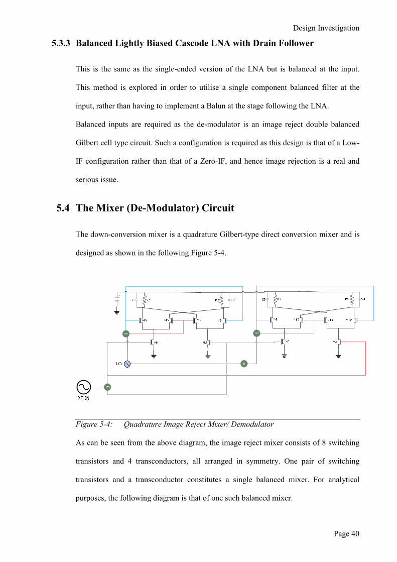
University of Bradford eThesis This thesis is hosted in Bradford Scholars – The University of Bradford Open Access repository. Visit the repository for full metadata or to contact the repository team
© University of Bradford. This work is licenced for reuse under a Creative Commons
Licence.
Page 2
CMOS DESIGN ENHANCEMENT TECHNIQUES
FOR RF RECEIVERS
Analysis, design and implementation of RF receivers with component enhancement and
component reduction for improved sensitivity and reduced cost, using CMOS
technology
Nandi Logan
Submitted for the degree of
Doctor of Philosophy
School of Engineering, Design and Technology
University of Bradford
2010
Page 3
i
Abstract
CMOS DESIGN ENHANCEMENT TECHNIQUES
FOR RF RECEIVERS
Analysis, design and implementation of RF receivers with component enhancement and
component reduction for improved sensitivity and reduced cost, using CMOS
technology
Keywords
RF Receivers, Inductors, Noise Figure, Component Quality Factor, CMOS, Sensitivity,
Compression Point, LNA, UMTS
Silicon CMOS Technology is now the preferred process for low power wireless
communication devices, although currently much noisier and slower than comparable
processes such as SiGe Bipolar and GaAs technologies. However, due to ever-reducing
gate sizes and correspondingly higher speeds, higher Ft CMOS processes are
increasingly competitive, especially in low power wireless systems such as Bluetooth,
Wireless USB, Wimax, Zigbee and W-CDMA transceivers. With the current 32 nm gate
sized devices, speeds of 100 GHz and beyond are well within the horizon for CMOS
technology, but at a reduced operational voltage, even with thicker gate oxides as
compensation.
This thesis investigates newer techniques, both from a systems point of view and at a
circuit level, to implement an efficient transceiver design that will produce a more
sensitive receiver, overcoming the noise disadvantage of using CMOS Silicon. As a
starting point, the overall components and available SoC were investigated, together
with their architecture.
Two novel techniques were developed during this investigation. The first was a high
compression point LNA design giving a lower overall systems noise figure for the
receiver. The second was an innovative means of matching circuits with low Q
components, which enabled the use of smaller inductors and reduced the attenuation
loss of the components, the resulting smaller circuit die size leading to smaller and
lower cost commercial radio equipment. Both these techniques have had patents filed by the University.
Finally, the overall design was laid out for fabrication, taking into account package
constraints and bond-wire effects and other parasitic EMC effects.
Page 4
ii
Table of Contents
1 Introduction ........................................................................................................... 10
1.1 References ....................................................................................................... 11
1.2 Aims and Objectives ......................................................................................... 1
1.2.1 Introduction ................................................................................................... 1
1.3 Review of Literature ......................................................................................... 1
1.4 Layout of the Thesis .......................................................................................... 2
1.5 References ......................................................................................................... 4
2 Theory ...................................................................................................................... 5
2.1.1 CMOS and the Silicon Process ..................................................................... 5
2.2 Derivation of the I/V characteristics ................................................................. 7
2.2.1 First order effects .......................................................................................... 7
2.2.2 Second order effects ...................................................................................... 9
2.2.3 Parasitic model (MOS device capacitance)................................................. 10
2.2.4 MOS small signal model ............................................................................. 12
2.3 References ....................................................................................................... 14
3 Wireless Receivers ................................................................................................. 16
3.1 Introduction ..................................................................................................... 16
3.1.1 Antenna ....................................................................................................... 17
3.1.2 Front-End Duplexer .................................................................................... 17
3.1.3 Band-Pass filter ........................................................................................... 18
3.1.4 Power Amplifier and Low-Pass Filter......................................................... 19
3.1.5 Low Noise Amplifier .................................................................................. 20
3.1.6 Mixer/Demodulator ..................................................................................... 21
3.2 Conclusion ...................................................................................................... 23
3.3 References ....................................................................................................... 24
4 Types of Receiver Systems.................................................................................... 26
4.1 Introduction ..................................................................................................... 26
4.2 Superheterodyne Receiver .............................................................................. 26
4.3 Hartley/Weaver Method Receivers ................................................................. 27
4.4 Direct Conversion Receivers .......................................................................... 29
4.5 Conclusion ...................................................................................................... 31
4.6 References ....................................................................................................... 32
5 Design Investigation .............................................................................................. 34
5.1 Introduction ..................................................................................................... 34
5.2 Sensitivity requirements for WCDMA Receivers........................................... 34
5.3 The LNA ......................................................................................................... 36
5.3.1 Typical Cascode LNA ................................................................................. 36
5.3.2 Low biased cascode LNA with Drain Follower .......................................... 37
5.3.3 Balanced Lightly Biased Cascode LNA with Drain Follower .................... 40
5.4 The Mixer (De-Modulator) Circuit ................................................................. 40
5.5 The Capacitor .................................................................................................. 42
5.6 The Resistor .................................................................................................... 42
5.7 The Inductor .................................................................................................... 43
5.7.1 More accurate analysis of the inductor ....................................................... 47
5.8 Conclusion ...................................................................................................... 53
5.9 References ....................................................................................................... 54
6 Analysis of the High Compression Point LNA ................................................... 56
Page 5
iii
6.1 Initial Simulation and Analysis of High Compression Point LNA ................. 56
6.2 The method of achieving the increased compression point ............................ 58
6.3 References ....................................................................................................... 65
7 Design and Simulation of the LNA ...................................................................... 66
7.1 Typical Cascode LNA ..................................................................................... 68
7.1.1 Input and output return losses ..................................................................... 69
7.1.2 LNA Forward Gain ..................................................................................... 70
7.1.3 LNA Noise Figure ....................................................................................... 71
7.1.4 LNA 1 dB Compression Point .................................................................... 72
7.1.5 LNA Current Consumption ......................................................................... 73
7.2 Single-ended low biased Cascode LNA with drain follower .......................... 73
7.2.1 Proposed Single-ended LNA Input and Output Return Loss [1] ................ 74
7.2.2 Proposed Single-ended Forward Gain ........................................................ 76
7.2.3 Proposed Single-ended LNA Noise Figure ................................................. 78
7.2.4 Proposed Single-ended LNA Compression Point Curve ............................ 80
7.2.5 Proposed Single-ended LNA Current Consumption Analysis .................... 82
7.3 Balanced low biased Cascode LNA with drain follower ................................ 82
7.3.1 Proposed Balanced LNA Input and Output Return Loss ............................ 84
7.3.2 Proposed Balanced LNA Forward Gain ..................................................... 86
7.3.3 Proposed Balanced LNA Noise Figure ....................................................... 87
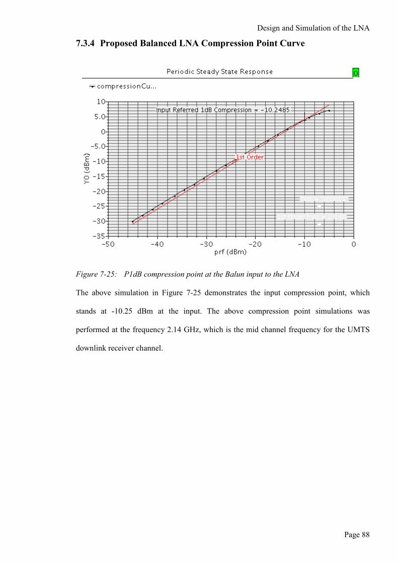
7.3.4 Proposed Balanced LNA Compression Point Curve .................................. 88
7.4 References ....................................................................................................... 89
8 Design and Simulation Results of Mixer/De-Modulator ................................... 90
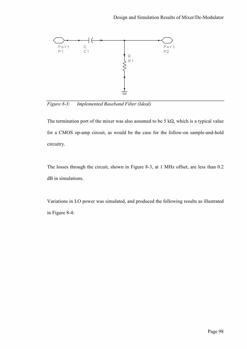
8.1 Mixer Calculations .......................................................................................... 95
8.2 Simulated Performance ................................................................................... 95
8.3 Other Design Issues ................................................................................... 100
8.4 Schematic Diagram of the Mixer .................................................................. 101
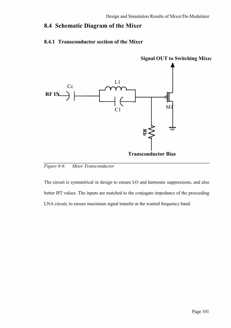
8.4.1 Transconductor section of the Mixer ........................................................ 101
8.4.2 The upper switching section of the mixer ................................................. 102
8.5 Simulated performance of the Mixer/De-Modulator .................................... 103
8.5.1 Input and Output Return Loss of the Mixer .............................................. 103
8.5.2 Mixer/De-Modulator Gain ........................................................................ 105
8.5.3 Noise Figure and output Noise Spectral Density ...................................... 106
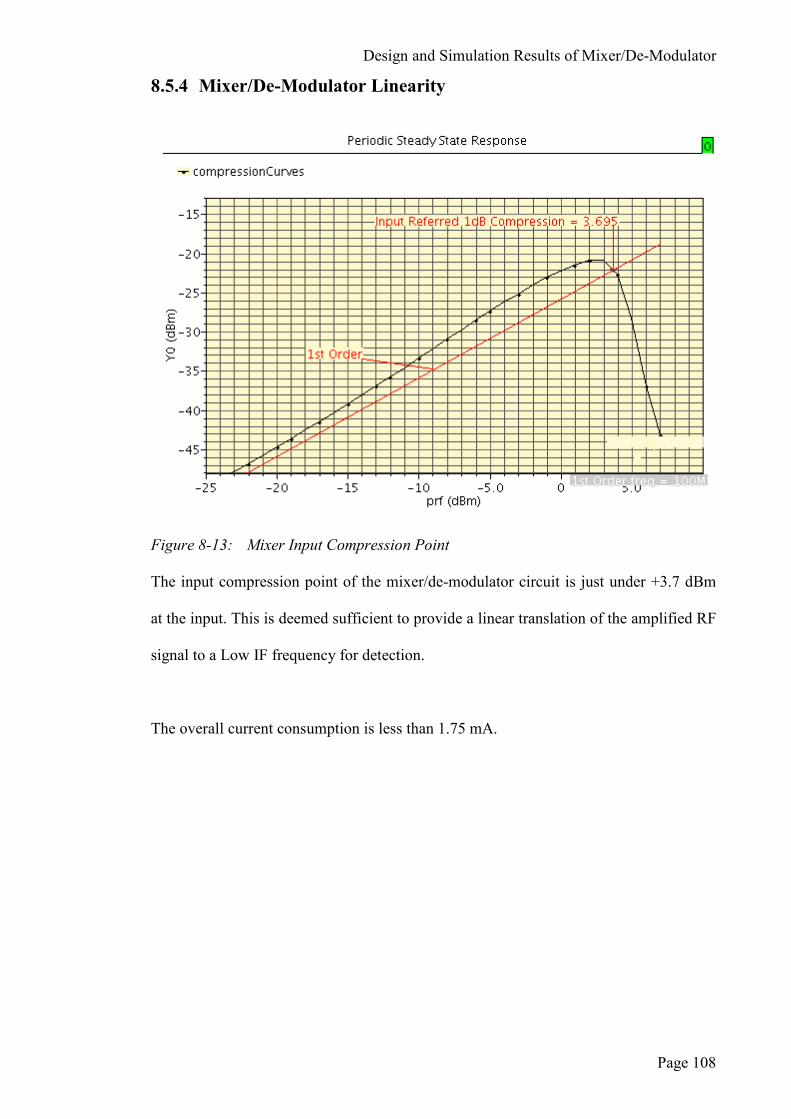
8.5.4 Mixer/De-Modulator Linearity ................................................................. 108
8.6 References ..................................................................................................... 109
9 Layout .................................................................................................................. 110
9.1 The LNA Layout ........................................................................................... 111
9.2 The Mixer Layout ......................................................................................... 113
9.3 The Complete Receiver Layout .................................................................... 114
9.4 Package ......................................................................................................... 115
9.5 References ..................................................................................................... 117
10 Design and Simulation of Overall Receiver System ......................................... 118
10.1 Conventional LNA Receiver System ............................................................ 118
10.1.1 Conventional Cascode LNA Systems Gain .......................................... 119
10.1.2 Conventional Cascode LNA Systems Noise ......................................... 120
10.1.3 Conventional Cascode LNA Receiver Linearity................................... 122
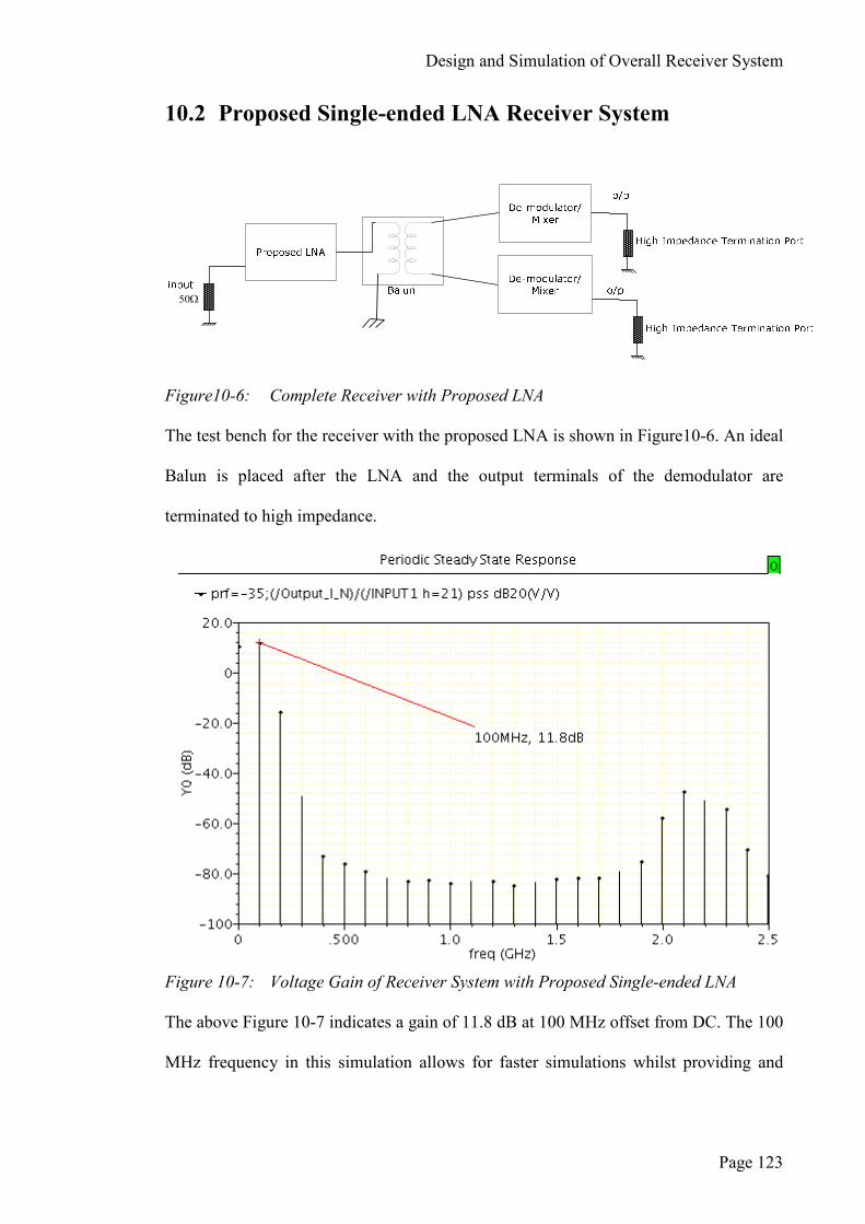
10.2 Proposed Single-ended LNA Receiver System............................................. 123
10.2.1 Systems Noise ....................................................................................... 124
10.2.2 Receiver Linearity ................................................................................. 125
10.3 Balanced LNA Receiver System ................................................................... 126
10.3.1 Systems Gain ......................................................................................... 126
10.3.2 Systems Noise ....................................................................................... 127
Page 6
iv
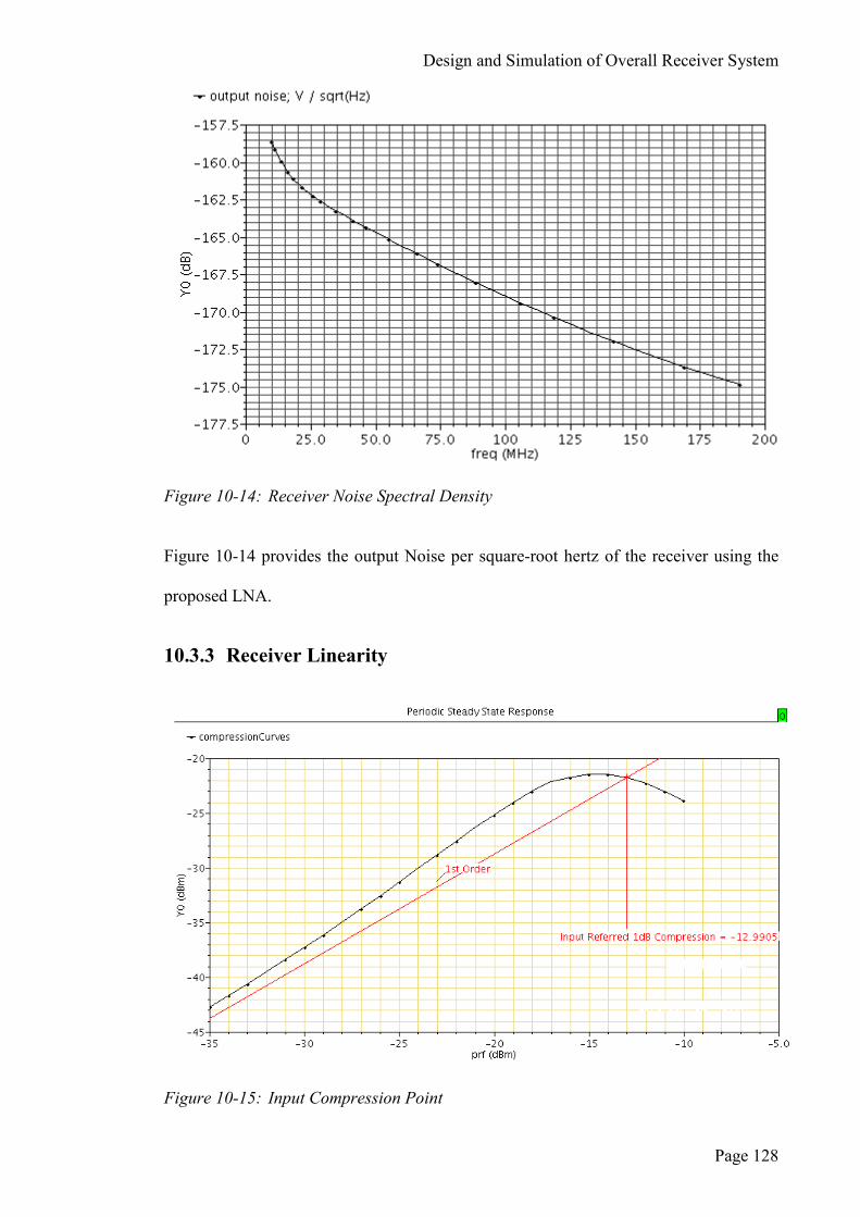
10.3.3 Receiver Linearity ................................................................................. 128
11 Results Summary and Discussion ...................................................................... 130
11.1 Results comparison and commentary against other available work: ............ 131
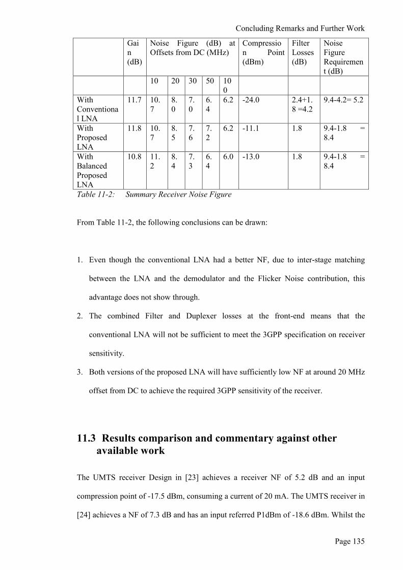
11.2 Receiver Results Summary ........................................................................... 134
11.3 Results comparison and commentary against other available work ............. 135
11.4 References ..................................................................................................... 137
12 Concluding Remarks and Further Work ......................................................... 140
12.1 Conclusions ................................................................................................... 140
12.2 Recommendations for further work .............................................................. 142
12.3 References ..................................................................................................... 144
Appendix 1 ................................................................................................................... 145
Administration and maintenance of the Cadence software ....................................... 145
Knowledge of Cadence Design Framework II ...................................................... 145
Installing simulation the software ......................................................................... 146
Managing and troubleshooting licenses ................................................................ 146
Working with technology data .............................................................................. 147
Design management and the Library Manager ..................................................... 147
Appendix 2 ................................................................................................................... 148
LIST OF AUTHOR PUBLICATIONS ..................................................................... 148
Journal articles (published): ...................................................................................... 148
Appendix 3 ................................................................................................................... 149
NMOS optimum width selection graph .................................................................... 149
Appendix 4 ................................................................................................................... 150
Filter Characteristics ................................................................................................. 150
Appendix 5 ................................................................................................................... 152
AustriamicrosystemsTM
Process Noise Models ......................................................... 152
Page 7
v
List of Figures
Figure 2-1: N-Channel MOSFET ................................................................................. 7
Figure 2-2: Semiconductor bar .................................................................................... 8
Figure 2-3: Symbolised MOS Device Parasitic Capacitance .................................... 11
Figure 2-4: MOS Device Parasitic Capacitance (Layout) ......................................... 11
Figure 2-5: Overlap Capacitive Regions ................................................................... 12
Figure 2-6: Spice Model of MOS Device .................................................................. 14
Figure 3-1: Systems Diagram of a Direct Conversion Receiver ............................... 18
Figure 3-2: Direct Conversion mixing issues ............................................................ 23
Figure 4-1: Superheterodyne Receiver Architecture ................................................. 28
Figure 4-2: The Hartley Image Reject Architecture .................................................. 29
Figure 4-3: The Weaver Image Reject Architecture .................................................. 30
Figure 4-4: The Direct Conversion Receiver ............................................................. 30
Figure 5-1: Cascode LNA and equivalent circuit ...................................................... 37
Figure 5-2: Low Biased Cascode LNA with Drain Follower .................................... 39
Figure 5-3: LNA Bondwire connection method ........................................................ 39
Figure 5-4: Quadrature Image Reject Mixer/ Demodulator....................................... 41
Figure 5-5: Spiral Inductor and its Parasitic Model ................................................... 45
Figure 5-6: Positive Mutual Inductance ..................................................................... 50
Figure 5-7: Parallel Resonance Graph ....................................................................... 52
Figure 5-8: Improvements in "Q" at Resonance with a parallel C with the L ........... 53
Figure 6-1: P1dB Compression Curve for LNA ........................................................ 58
Figure 6-2: LNA Equivalent Circuit of the 1st stage (Cascode) ................................. 62
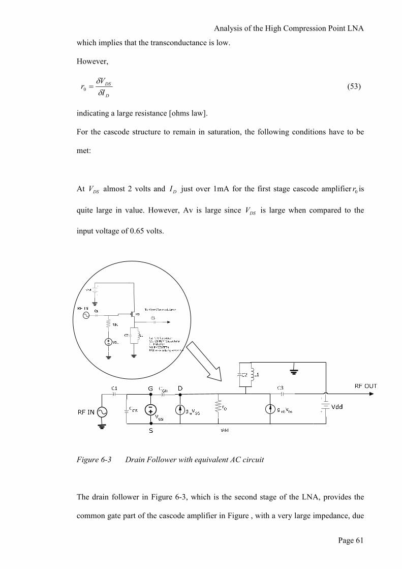
Figure 6-3 Drain Follower with equivalent AC circuit ............................................. 63
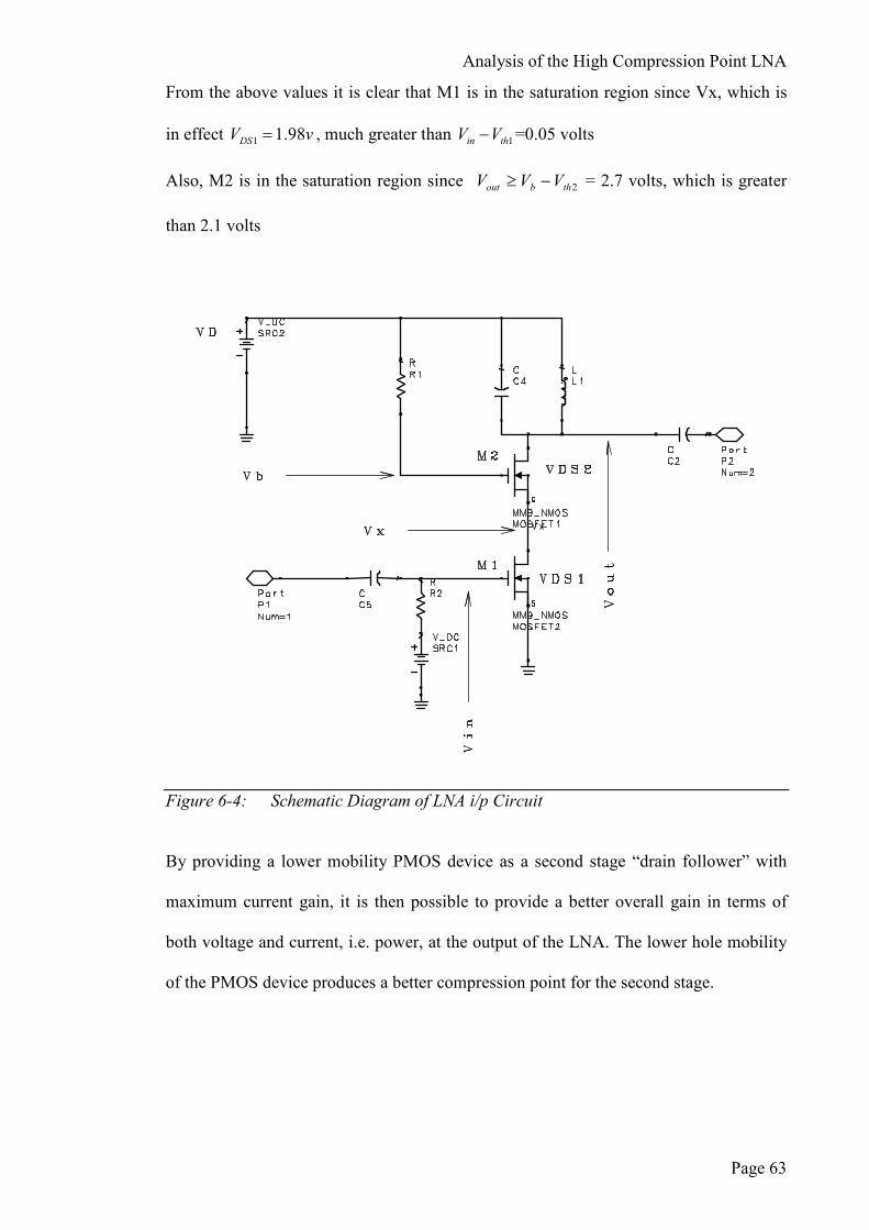
Figure 6-4: Schematic Diagram of LNA i/p Circuit .................................................. 65
Figure 7-1: Single Section of the Balanced LNA Cadence Schematic Entry ............ 68
Figure 7-2: Conjugate Plot of LNA Output and Mixer Input .................................... 69
Figure 7-3: Typical Cascode LNA Input and Output Port Voltage Reflection
Coefficients........ ............................................................................................................. 70
Figure 7-4: Typical Cascode LNA Return losses (log magnitude) ............................ 71
Figure 7-5: Typical Cascode LNA Forward Gain ..................................................... 72
Figure 7-6: Typical Cascode LNA Noise Figure ....................................................... 72
Figure 7-7: Typical Cascode LNA Compression Point Plot ...................................... 73
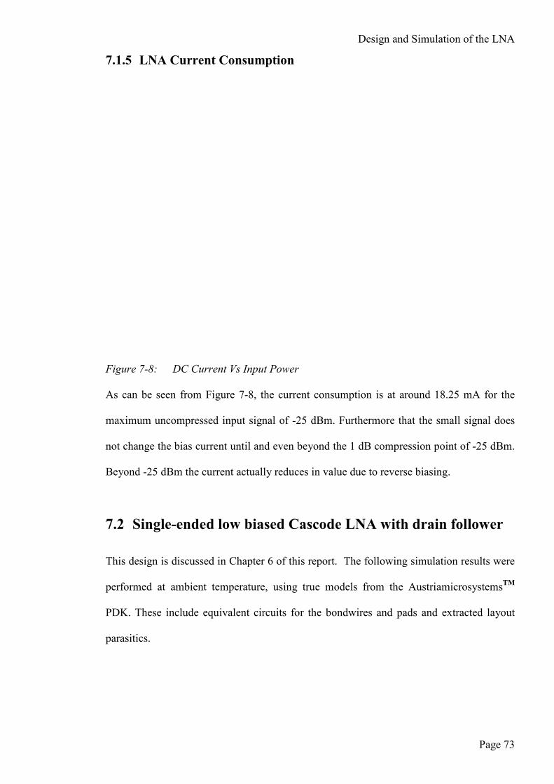
Figure 7-8: DC Current Vs Input Power .................................................................... 74
Figure 7-9: Single-ended LNA Test Bench ............................................................... 75
Figure 7-10: Input and Output Port Voltage Wave Reflection Coefficient ................ 75
Figure 7-11: Simulated Input and Output Port Return Losses ..................................... 76
Figure 7-12 Measured Input and Output Return Losses of the Single ended LNA ........ 77
Figure 7-13: Simulated Forward Voltage Gain of the proposed single-ended LNA ... 78
Figure 7-14 Measured Forward Voltage Gain of the proposed single-ended LNA ........ 78
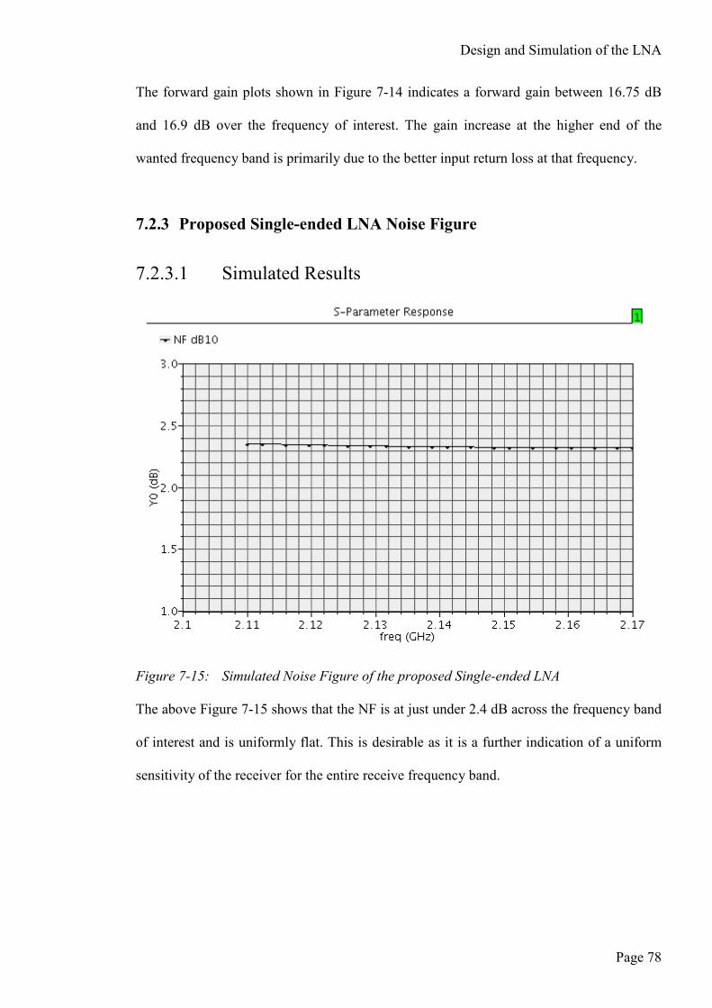
Figure 7-15: Simulated Noise Figure of the proposed Single-ended LNA.................. 79
Figure 7-16 Measured Noise Figure of the proposed Single-ended LNA ...................... 80
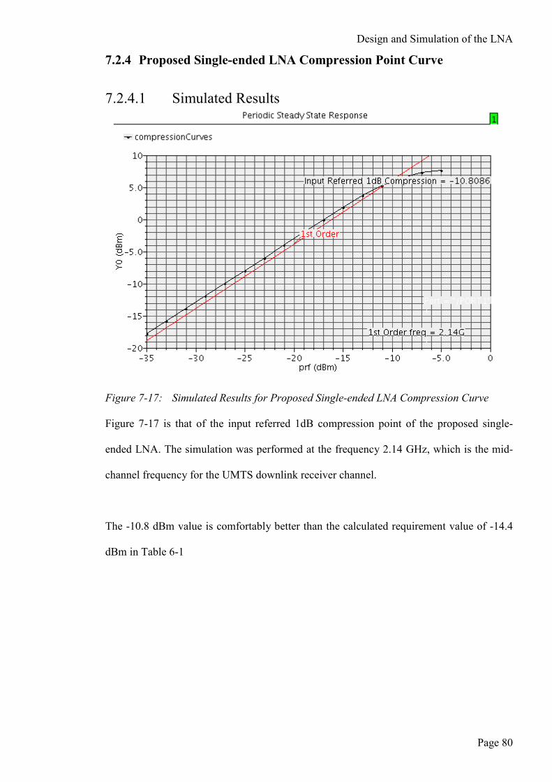
Figure 7-17: Simulated Results for Proposed Single-ended LNA Compression Curve
.................................................................................................................81
Figure 7-18 Measured Results for Proposed Single-ended LNA Compression Curve ... 82
Figure 7-19: Proposed Single-ended LNA Current Consumption vs Input Power
Curve .................................................................................................................83
Figure 7-20: Balanced LNA Test Bench...................................................................... 84
Figure 7-21: Balanced LNA Input and Output Port Voltage Reflection Coefficient .. 85
Page 8
vi
Figure 7-22: Balanced Input and Output Port Voltage Reflection Coefficient ........... 86
Figure 7-23: Proposed Balanced LNA Forward Voltage Gain .................................... 87
Figure 7-24: Noise Figure for the proposed Balanced LNA ........................................ 88
Figure 7-25: P1dB compression point at the Balun input to the LNA ......................... 89
Figure 8-1: Proposed Single-Ended LNA Out of band gain ...................................... 91
Figure 8-2: Complete Receiver De-Modulator (Mixer) ............................................. 93
Figure 8-3: Implemented Baseband Filter (Ideal) ...................................................... 98
Figure 8-4: Receiver NF vs LO Power ...................................................................... 99
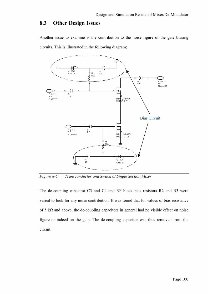
Figure 8-5: Transconductor and Switch of Single Section Mixer ........................... 100
Figure 8-6: Mixer Transconductor ........................................................................... 101
Figure 8-7: Upper Switching Section of Mixer ( In Cadence Schematic Entry) ..... 102
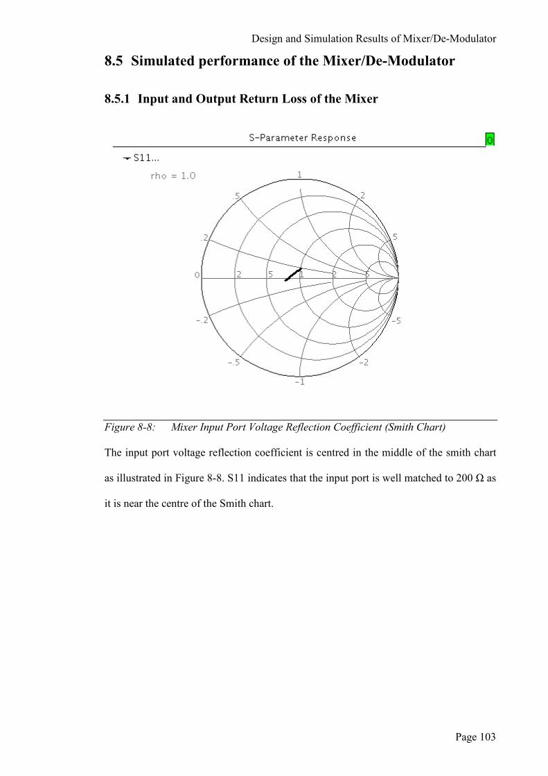
Figure 8-8: Mixer Input Port Voltage Reflection Coefficient (Smith Chart) .......... 103
Figure 8-9: Log Magnitude of Mixer Input Port Voltage Reflection Coefficient .. 104
Figure 8-10: Voltage Gain of Mixer (Periodic Steady State response) ..................... 105
Figure 8-11: Mixer Noise Figure ............................................................................... 106
Figure 8-12: Mixer Noise Spectral Density dB/ Hz ............................................... 107
Figure 8-13: Mixer Input Compression Point ............................................................ 108
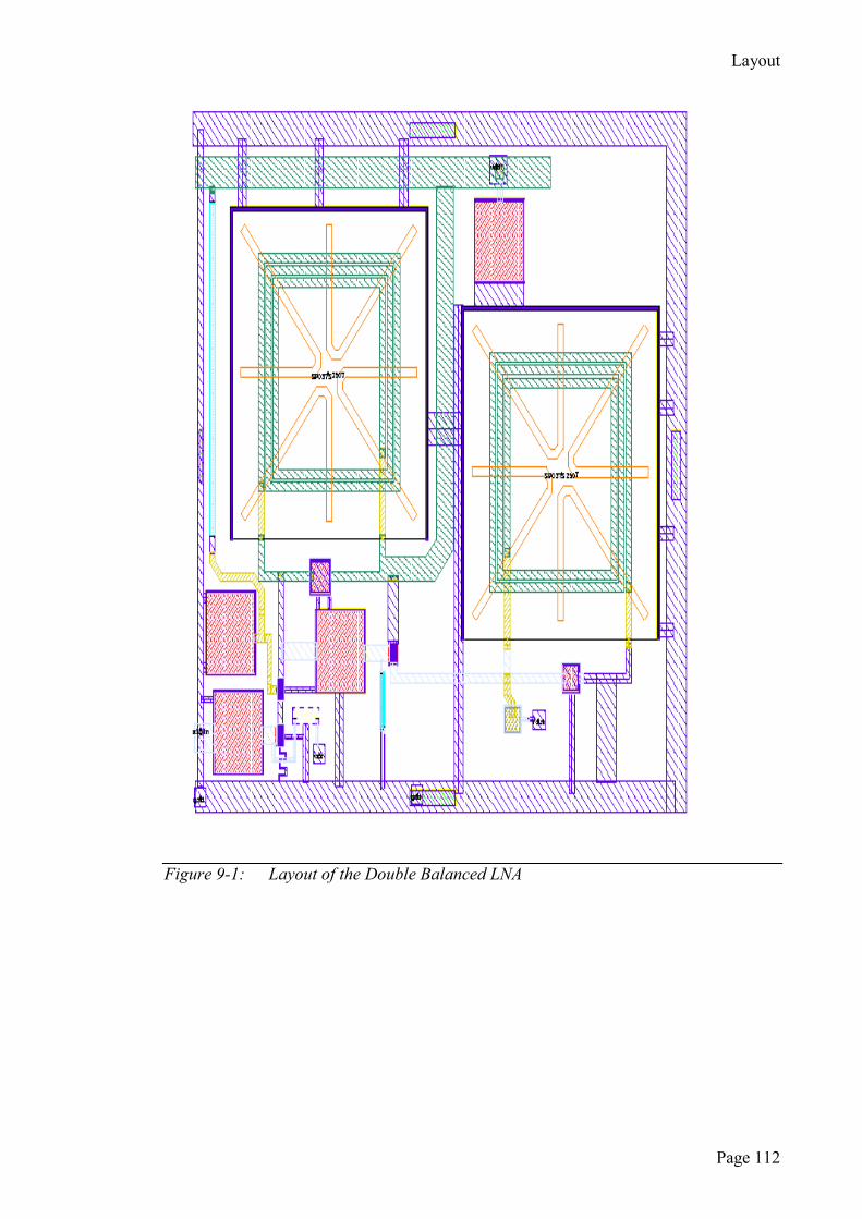
Figure 9-1: Layout of the Double Balanced LNA ................................................... 112
Figure 9-2: Layout of the Mixer Transconductor .................................................... 113
Figure 9-3: Layout of the Switching Section of the Mixer (De-Modulator) ........... 114
Figure 9-4: Complete Receiver Layout (Including Bond wire Pads) ...................... 115
Figure 9-5: JBP-X Package Diagram ....................................................................... 116
Figure 10-1: Conventional LNA Receiver Test Bench .............................................. 118
Figure 10-2: Voltage Gain of Receiver System with Conventional LNA ................. 119
Figure 10-3: Noise Figure of Receiver System with Conventional LNA .................. 120
Figure 10-4: Noise Spectral Density of Receiver System with Conventional LNA .. 121
Figure 10-5: Input 1 dB Compression Point of Receiver System with Conventional
LNA ...............................................................................................................122
Figure 10-6: Complete Receiver with Proposed LNA ............................................... 123
Figure 10-7: Voltage Gain of Receiver System with Proposed Single-ended LNA .. 123
Figure 10-8: Noise Figure of Receiver System with Proposed Single-ended LNA .. 124
Figure 10-9: Noise Spectral Density of Receiver System with Proposed Single-ended
LNA ...............................................................................................................125
Figure 10-10: Input 1dB Compression of Receiver System with Proposed Single-ended
LNA ...............................................................................................................125
Figure 10-11: Complete Cadence Implementation of Receiver Circuit ...................... 126
Figure 10-12: Periodic AC Response of Receiver Gain .............................................. 126
Figure 10-13: Receiver Noise Figure ........................................................................... 127
Figure 10-14: Receiver Noise Spectral Density ........................................................... 128
Figure 10-15: Input Compression Point ....................................................................... 128
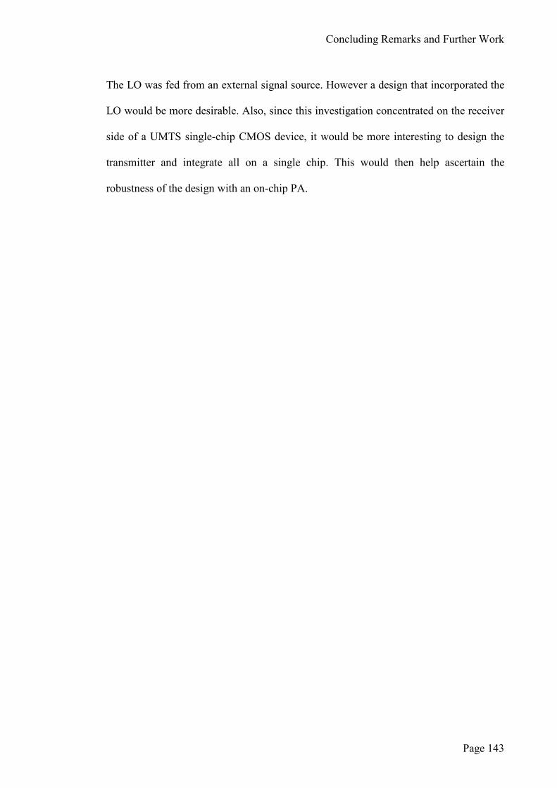
Figure A-1: FT Plot for NMOS Device - Datasheet for EPCOS Ceramic Microwave
Duplexer A260, at ambient temperature. ...................................................................... 150
Figure A-2: W-CDMA Front-End Duplexer for UMTS - Plots from the EPCOS
Ceramic Rx Filter B7752 at ambient temperature ........................................................ 151
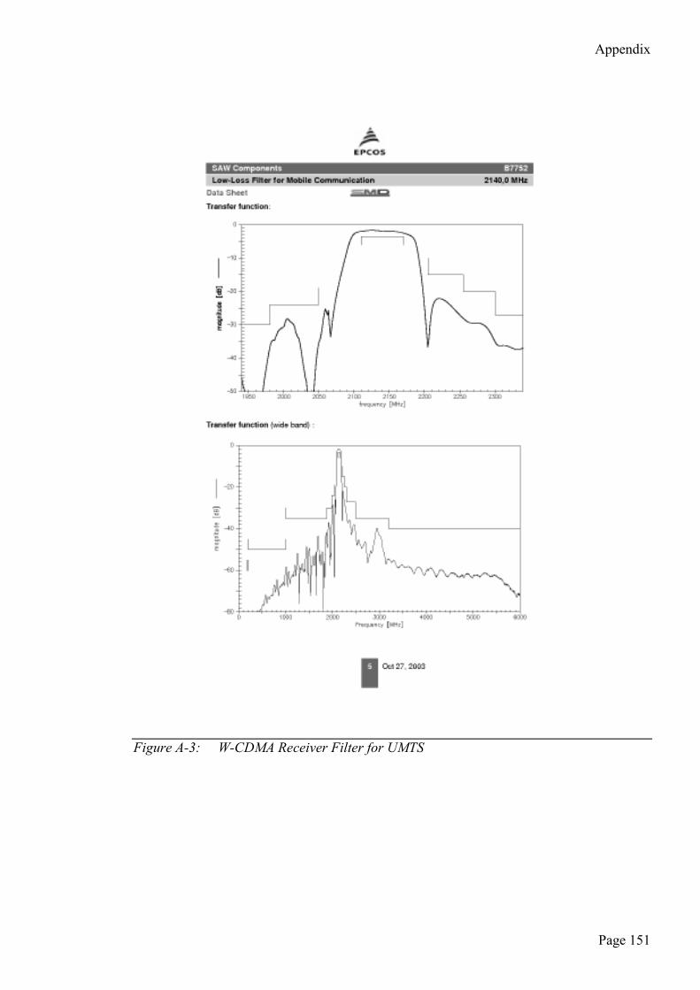
Figure A-3: W-CDMA Receiver Filter for UMTS ................................................... 152
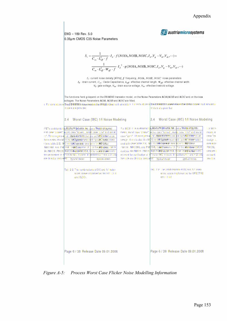
Figure A-4: Process Flicker Noise Modelling Information ...................................... 153
Figure A-5: Process Worst Case Flicker Noise Modelling Information................... 154
Figure A-6: Process Thermal Noise Curves ............................................................. 155
Figure A-7: NMOS Noise Curves for W/L 10/10µm ............................................... 156
Figure A-8: PMOS Noise Curves for W/L 10/10µm ................................................ 157
Page 9
vii
List of Tables
Table 3-1: Duplexer Performance table ....................................................................... 19
Table 3-2: RX Filter Performance table ....................................................................... 20
Table 5-1: Systems Noise Budget for Receiver ............................................................ 36
Table 5-2: Calculated Inductor values .......................................................................... 48
Table 5-3: Inductor Comparison table .......................................................................... 48
Table 6-1 Maximum Transmitter Signal at LNA input ............................................... 59
Table 6-2: LNA Bias Voltages .................................................................................... 64
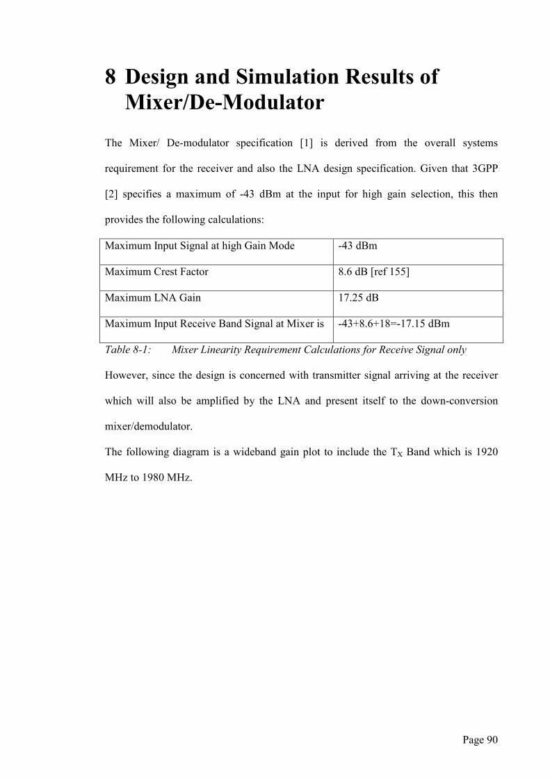
Table 8-1: Mixer Linearity Requirement Calculations for Receive Signal only .......... 90
Table 8-2: Mixer Linearity RequirementCalculation withTransmitter Signal present . 91
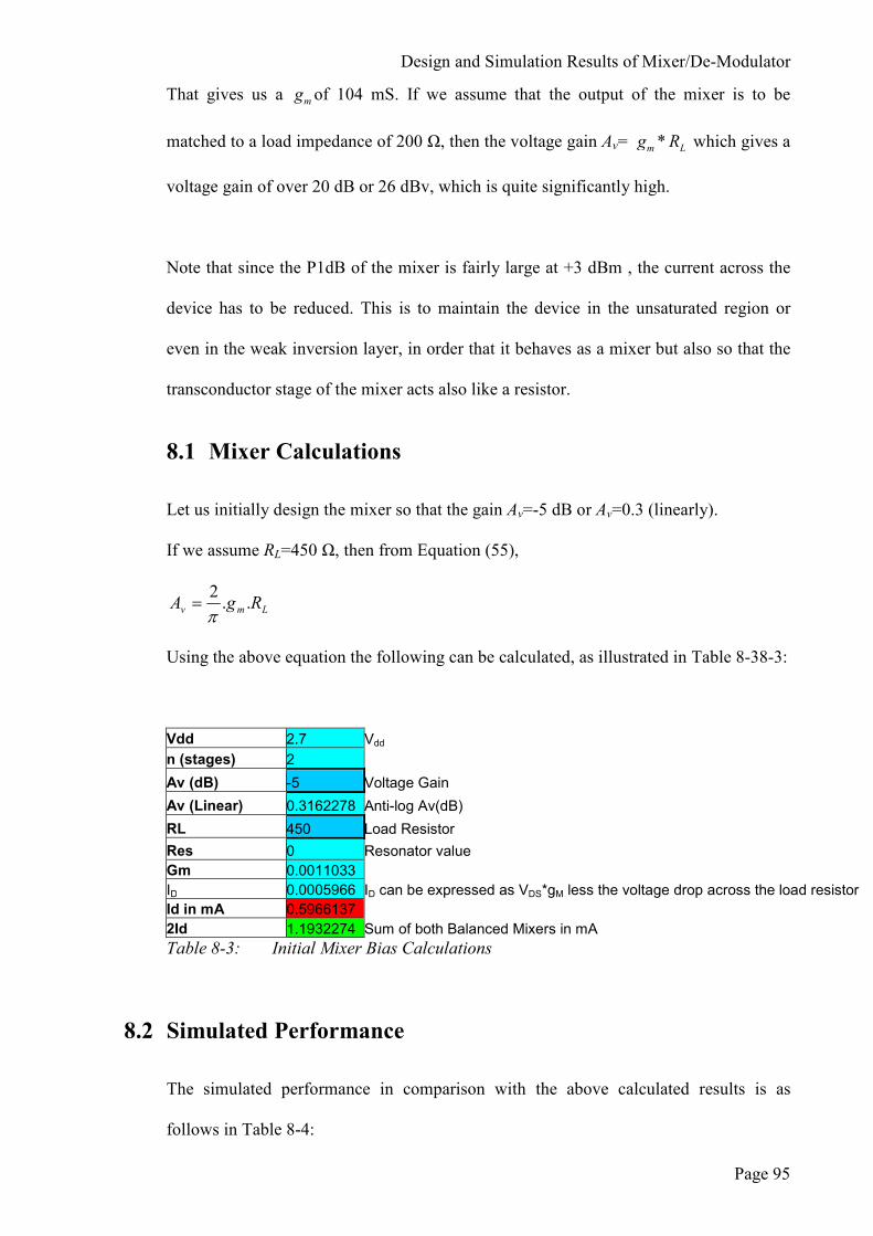
Table 8-3: Initial Mixer Bias Calculations .................................................................... 95
Table 8-4: Simulated Mixer Bias Results ..................................................................... 96
Table 11-1: Summary of LNA Noise Figure ................................................................ 130
Table 11-2: Summary Receiver Noise Figure ............................................................... 130
Page 10
viii
Abbreviations
3GPP Third Generation Partnership Project
AC Alternating Current
AM Amplitude Modulation
ASIC Application Specific Integrated Circuit
CDMA Code Division Multiple Access
CMOS Complimentary Metal Oxide Silicon Transistor
dB Decibels
dBm Decibels with reference to one milliWatt
dBW Decibel Watts
DC Direct Current
DCR Direct Conversion Receiver
DRC Design Rules Check
DSP Digital Signal Processing
ESD Electrostatic Discharge
ESR Effective Series Resistance
FEM Front-End Module
Ft Unity Gain Point of Frequency Transition
GaAs Gallium Arsenate
GMD Geometric Mean Distance
IF Intermediate Frequency
I/V Current versus Voltage
IIP2 Input second Order Intercept Point
IIP3 Input third Order Intercept Point
Page 11
ix
LIF Low Intermediate Frequency
LNA Low Noise Amplifier
LO Local Oscillator
MIM Metal Insulation Metal (capacitor)
MOSFET Metal Oxide Semiconductor Field Effect Transistor
NF Noise Figure
NMOS N-Type Metal Oxide Silicon Transistor
PA Power Amplifier
PMOS P-Channel Metal Oxide Silicon Transistor
PVT Process Voltage and Temperature
Q Quality Factor
RF Radio Frequency
SAW Surface Acoustic Wave
SiGe Silicon Germanium
SoC System on Chip
SPICE Simulation Program with Integrated Circuit Emphasis
S.R.F Self Resonance Frequency
SW Switch/Duplexer
UMTS Universal Mobile Telecommunications Standard
V Voltage
VCO Voltage Controlled Oscillator
WCDMA Wide-Band Coded Division Multiple Access
WLAN Wireless Local Area Network
WPAN Wireless Personal Area Network
ZIF Zero Intermediate Frequency
Page 12
10
1 Introduction
The unmistakable trend over the last decade and a half in mobile hand terminal design
has been an ever-increasing amount of integration as a means of reducing cost and
power consumption, especially for the cellular telecommunications industry.
A little over a decade ago, a single-band GSM cellular hand terminal would have
consisted of over 3000 components for the RF, Baseband and DC circuitry. However,
an equivalent entry-level quad-band cellular hand terminal today consists of around 30
components and is a clear indication of the amount of integration that has already taken
place over a relatively short time.
Impressive though the design integration has been, the overall design has still
maintained the principal division between analogue and digital circuitry, and
consequently is centred on two core ASIC chipsets. This is in contrast to related but
different WPAN and WLAN standards for which there has been greater success in
bridging this divide, to create the much-coveted System on Chip (SoC) design product.
The success in WPAN and WLAN has been in part due to the lower specification
requirements set by the relevant standards, particularly in terms of transmit power and
receiver sensitivity.
Therefore, the aim of this project was to enhance the RF analogue structures, thus
enabling Silicon CMOS technologies to be used more effectively in the implementation
of front-end cellular mobile hand terminals, especially for WCDMA 3G UMTS hand
terminals, designed to comply with 3GPP specification number 3GPP.TS.25.101 [1].
Page 13
Wireless Receivers
11
1.1 References
[1] The 3GPP UMTS Standard [online]. Available: http://www.3gpp.org
Page 14
Page 1
1.2 Aims and Objectives
1.2.1 Introduction
The aim of the work that was carried out was to design a complete receiver to comply
with the 3GPP specification [1] and in the process refine the system architecture and
circuit design methodology to provide overall improvements in the transceiver.
Given the complexities of the design requirements, it was envisaged that not all
components of the architecture could be implemented to achieve a true single-chip SoC
solution. This is in part due to the type of technology being used, and also to the cost
involved in fabrication.
Furthermore, given that the complete front-end has now been integrated by specialist
component makers like Murata/EPCOS and sold as a Front-End Module (FEM), it
makes far more sense to incorporate these developments.
Typically a FEM includes a front-end switch/Diplexer and SAW/band-pass filters, and
come matched to a characteristic impedance of 50 Ω.
1.3 Review of Literature
A number of books and papers have been reviewed including most of the IEEE journals
on solid state devices particularly from 1999 onwards. A number of IC manufacturers
have also relevant literature, downloadable from their websites. These include
Skyworks, Infineon, RFMD, Maxim, Triquint and TI.
The initial CMOS design for the receiver architecture is based on the preliminary
CMOS work carried out by Thomas H. Lee [2], with the design suggestions described
by Behazad Rezavi [3]. According to the LNA design described in [2], inductors at the
Page 15
Introduction
Page 2
gate and source of the CMOS LNA are manipulated to achieve the required impedance
values. The source inductor Ls was used to achieve the real part of the required
impedance transformation and the phase was achieved by the gate inductor Lg.
Furthermore, load impedance was provided by the drain inductor and the load capacitor.
The gain-boosting techniques described in [4] were studied for their potential to
improve the received gain characteristics. Various transistor topologies were
investigated based on the work carried out by Boom Kyu Ko [5]. Noise models
described by Jerome Le Ny in [6] were studied for their implications for the receiver
design.
The mixer/down-converter architectures were based on the work already carried out on
a BiCMOS design by Ranjit Gharpurey [7]. The direct conversion SiGe BiCMOS
receiver designed by Madjid Hafizi [8] was also studied and various design issues stated
taken onboard.
Finally, various test methods for accurately establishing the performance of the final
design were investigated. The very useful information provided by John Lukez in [9]
was particularly studied and used to verify the simulation data.
1.4 Layout of the Thesis
The thesis is laid out such that the reader is guided through each chapter, beginning with
the fundamental theory for CMOS technology and ending with the measurement results
and detailed analysis of the design. Chapter 2 describes the fundamental theory of the
CMOS technology, providing a quick but yet detailed insight into the technology,
highlighting a number of issues that influence high frequency designs in the technology.
Page 16
Introduction
Page 3
Chapter 3 describes the WCDMA wireless receiver design requirements as defined in
3GPP [1] and the different circuit components that are required in order to meet the
requirement specification. Whilst also emphasising the practical limitations of the
technology. Chapter 3 also introduces one of the fundamental goals of this thesis,
namely the reduction of overall components by employing novel design concepts into
the receiver design architecture.
Chapter 4 provides a detailed summary of the merits and drawbacks of various receiver
architectures and ends by justifying the most suitable architecture in order to achieve the
goals of this receiver designed in this thesis.
Chapter 5 provides a detailed analysis of the receiver design in order to meet the 3GPP
specification [1] and the design of the receiver itself based on these calculations. The
core circuits are the LNA and the Direct Conversion Image Reject Mixer and these two
circuits together with the various inductors and capacitors are thus part of the design
that is analysed in detail.
Chapters 6 & 7 provide a further detailed design analysis of the high compression point
LNA and the simulation and measurement results of this LNA. Chapter 8 provides a
detailed design analysis of the Image Reject Receiver Mixer together with the
simulation and measurement results. Chapter 9 provides a detailed account of the
physical layout of the receiver design whilst emphasising various design issues.
Chapter 10 provides the final post layout design simulation of the entire receiver and
finally Chapter 11 summaries all the results and discusses the significance of them.
Page 17
Introduction
Page 4
1.5 References
[1] The 3 GPP UMTS Standard [online]. Available: http://www.3gpp.org
[2] D. K Shaefer and T. H. Lee, “A 1.5v, 1.5 GHz CMOS Low Noise Amplifier”,
IEEE J Solid State Circuits, vol. 32, No.5, pp 745-759, May 1992.
[3] Behzad Rezavi, “Design Considerations for Direct-Conversion Receivers,”
IEEE Transactions on Circuits and Systems-II: Analog and Digital Signal Processing,
vol. 44, No.6, June 1997.
[3] S. Asgaran and M. Jamal Deen, “ A Novel Gain Boosting Technique for Design
of Low Power Narrow-Band RFCMOS LNA’s,” Poster Session IV Analog and Mixed
Signal Design, 2004.
[4] Boom Kyu Ko, Kwyro Lee, “A Comparative Study on the Various Monolithic
Low Noise Amplifier Circuit Topologies for RF and Microwave Applications,” IEEE J
Solid-State Circuits , vol. 31, No.8, August 1996.
[5] Jerome Le Ny, Bhavana Thudi, Jonathan Mc Kenna, “A 1.9 GHz Low Noise
Amplifier” EECS 552, Analog Integrated Circuits Project, Winter 2002.
[6] Ranjit Gharpurey, Naveen Yanduru, Francesco Dantoni et al, “A Direct
Conversion Receiver fro the 3G WCDMA Standard”, IEEE J Solid- State Circuits, vol.
38, No.3, March 2003.
[7] Madjid Hafizi, Shen Feng, Taoling Fu, Kim Schulze et al, “RF Front-End of
Direct Conversion Receiver RFIC fro CDMA-2000,” IEEE J Solid-State Circuits,
vol.39, No.10, October 2004.
[8] John Lukez, “New Test Approaches for Zero-IF Transceiver Devices,” SEMI
Technology Symposium: International Electronics Manufacturing Technology (IEMT)
Symposium, 2003.
Page 18
Page 5
2 Theory
2.1.1 CMOS and the Silicon Process
Digital circuitry has for long been the domain of CMOS technology. Its unsuitability for
analogue circuitry derives from its inferior speed and noise performance and is well
documented in [1-4].
Whilst a 0.35 µm SiGe Bipolar outperforms a similar 0.35 µm CMOS process in terms
of NF, Gain and current usage, CMOS still performs sufficiently well enough to design
substantial amounts of RF circuits[5]. This is further enhanced with improvements in
technology, namely the submicron and nanometre processes.
CMOS technology is now proving attractive for the design of analogue integrated
circuits [6], as a means of completely integrating the analogue and digital parts into a
single System on Chip (SoC). Current gate sizes have reduced to 60 nm for production
purposes giving a process Ft in excess of 60 GHz [7].
The cross section of a typical NMOS device is illustrated as in Figure 2-1 [8]:
Page 19
Theory
Page 6
Figure 2-1: N-Channel MOSFET
The MOSFET consists of two heavily doped n-type regions called the source and drain.
In between these heavily doped regions, a gate consisting of a heavily doped polysilicon
layer is placed. For an NMOS device, the entire structure sits in a lightly doped p-type
substrate, also known as the bulk. For a PMOS device, this structure sits in an n-well,
itself sitting within the lightly doped p-type substrate.
In an NMOS device, when a positive voltage is applied to the gate, holes are repelled
and at some threshold level of voltage, Vth, the channel becomes completely depleted of
charge. Further increases in voltage cause a gate-induced inversion layer of electrons
forming a conduction layer, which joins drain and source together. This conduction
layer is commonly known as the channel.
Ignoring the charge doping in the oxide layer, Vth can be expressed as follows [9]:
ox
dep
FmsthC
QV ++= φφ 2 (1)
where,
msφ is the difference between the polysilicon gate and the silicon substrate,
Page 20
Theory
Page 7
depQ is the charge in the depletion region and is equal to
subFsi NQqε4 , (2)
oxC is the gate oxide capacitance per unit area,
)ln(i
subF
n
N
q
kT=φ , (3)
Where
q is the electron charge,
subN is the doping concentration of the substrate, and
siε is the dielectric constant of silicon.
2.2 Derivation of the I/V characteristics
2.2.1 First order effects
Figure 2-2: Semiconductor bar
Consider the semiconductor bar carrying current I in Figure2-2, where I can be
represented as [9]
I=Qd.v (4)
in which Qd is the charge density in Coulombs per metre and v the velocity of the
charge. At the onset of inversion, when the gate voltage Vgs > Vth, any excessive charge
I
v
Page 21
Theory
Page 8
that appears on the gate is mirrored by the channel [9], providing a channel charge equal
to
Qd = W.Cox(Vgs – Vth) (5)
where Cox is the gate oxide capacitance per unit area and W is the width of the channel.
If the drain voltage VD is of a value greater than zero and the source voltage VS is zero
volts, then for an applied gate voltage VG the channel potential varies from VG to VG-VD.
At a point x along the channel, the charge density is given by [9],
Qd(x)=W . Cox (VGS-V(x)-Vth) (6)
For semiconductors, v=µ E where µ is the electron mobility and E the electric field.
The electric field is also described as the rate of change of voltage per unit distance [9]
i.e.
E(x) = -dV/dx, so
ID=W . oxC . [VGS - V(x) – Vth] nµ [d(Vx)/dx] (7)
Imposing boundary conditions V(0) = 0; V(L) = DSV and integrating on both sides
ID = ]2
1)[(
2
DSDSthGSoxn VVVVL
WC −−µ (8)
At saturation )( thGSDS VVV −= (9)
which implies that ID = 2][
2
1thGSoxn VV
L
WC −µ (10)
For PMOS devices a negative sign is added to the above equation. Hole mobility is 1/2
to 1/3 the mobility of electrons, which implies a lower current drive capability.
From equation (10) the transconductance ( mg ) of the device can be derived as,
GS
Dm
V
Ig
δδ
= . (11)
At conditions of saturation, the mg is derived as
Page 22
Theory
Page 9
)( thGSoxnm VVL
WCg −= µ , (12)
and in the linear triode region
DSoxnm VL
WCg µ= . (13)
2.2.2 Second order effects
For submicron devices, the second order effects must be taken into account, in order to
ascertain the true functionality of the devices.
2.2.2.1 The body effect or the back gate effect (γ )
The bulk voltage VB can act as a second gate in CMOS devices. As VB becomes more
negative, the holes in the channel are attracted to the substrate connection leaving
negative charge behind. This causes the depletion region to become wider than
intended. Also, as VB increases then Vth also increases. This is expressed as follows [10]:
)22(0 FSBFthth VVV φφγ −++= (14)
where ox
subsi CNq )2( εγ = (15)
Nsub and Cox are usually balanced out to give reasonable values of γ.
2.2.2.2 Channel length modulation (λ)
As the potential between the gate and the drain increases, the actual length of the
channel decreases. In other words, the effective channel length 'L is a function of VDS
[11].
Page 23
Theory
Page 10
where LLL ∆−=' and DSVL
L.λ=
∆. (16)
Thus )1(][2
1 2
DSthGSoxnD VVVL
WCI λµ +−= . (17)
The channel length modulation becomes more pronounced for shorter channel lengths,
making the device behave less like an ideal current source.
2.2.3 Parasitic model (MOS device capacitance)
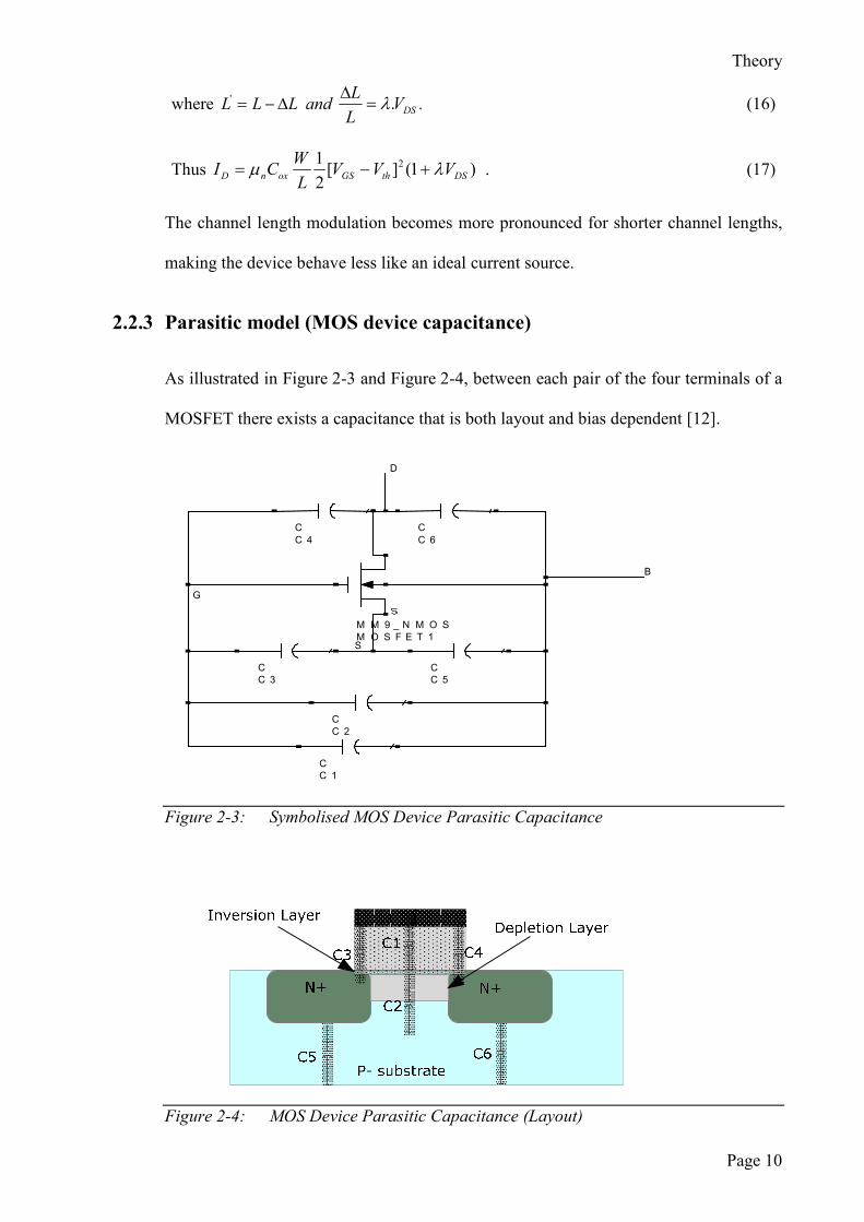
As illustrated in Figure 2-3 and Figure 2-4, between each pair of the four terminals of a
MOSFET there exists a capacitance that is both layout and bias dependent [12].
Figure 2-3: Symbolised MOS Device Parasitic Capacitance
Figure 2-4: MOS Device Parasitic Capacitance (Layout)
G
B
D
S
C
C 1
C
C 2
C
C 4
C
C 5
C
C 3
C
C 6
M M 9 _ N M O S
M O S F E T 1
Page 24
Theory
Page 11
2.2.3.1 Oxide capacitance C1
C1, oxide capacitance between the gate and the channel, is given by [12]
oxW.L.CC1 = (18)
2.2.3.2 Depletion capacitance C2
C2, depletion capacitance between the channel and the substrate, is given as [12].
Fsubsi /2φNqεW.LC2 = (19)
Capacitance C1 and C2 added together are commonly referred to as the gate bulk
capacitance CGB.
2.2.3.3 Overlap capacitances C3 and C4
C3 and C4 are the gate-poly overlap capacitances with the source (CGS) and drain (CGD)
region respectively, and are layout and process dependent. COV, the overlap capacitance
per unit area is used to calculate this value [12]
Figure 2-5: Overlap Capacitive Regions
As illustrated in Figure 2-5, the following capacitance values can be calculated:
When the device is off, then [12]
CGD=CGS=COVW (20)
CGS
TRIODE
Saturation
OFF
WCOV
2/3WLCOX+WCOV
OVWCOXWLC
+2
VGS VD-VTH
CGD
VTH
Page 25
Theory
Page 12
When the device is in the deep triode region, the gate voltage draws equal amount of
charge from both the Drain and Source [12].Thus,
CGD=CGS=WLCOX/2 + WCOV (21)
where W is the width of the channel and L is the length of the channel specified in µm
and overlap capacitance Cov is specified in fF [12]. However, when the device is in
saturation,
CGS=2/3WLCOX+WCOV (22)
2.2.3.4 Junction capacitance
C5 and C6 are the junction capacitances between the source and the drain area and are
further subdivided as the bottom plate junction capacitor, denoted by Cj, and the
sidewall junction capacitor [13], denoted CjSW.
Each of the junction capacitors can be expressed as
Cjo/[1+VR/ΦB]m (23)
VR is the reverse voltage across the junction and ΦB is the junction built-in potential,
with m typically 0.3 to 0.4.
2.2.4 MOS small signal model
Small signal models are derived by producing small signal increments in bias point and
calculating the resulting increments in other bias parameters.
From equation (8), it was established the ID is primarily a function of VGS and from
equation (11) it was established that mg is the derivative of ID with VGS. In equation (17)
the concept of channel length modulation, which was dependent on VDS, was
Page 26
Theory
Page 13
introduced. However, a current source that is dependent upon the voltage across it can
be represented by a resistor r0, where,
D
DS0
δI
δVr = (24)
In equation (14) the body effect was derived and its effect on the threshold voltage was
described. With all other parameters held constant, it could be concluded that the body
effect acts as a second current source and that ID is a function of the bulk voltage. These
can then be modelled by voltage-dependent current sources and together with the device
capacitances, the complete MOS small signal model [14] can be sketched as follows in
Figure 2- 6
Figure 2- 6: Spice Model of MOS Device
VGS
S
G D
gmVGS gmVbS
ro
B
CGB
CGS
CGD
CSB
CDB
Page 27
Theory
Page 14
2.3 References
[1] A. A. Abid, “High Frequency Noise Measurements on FETs with Small
Dimensions,” IEEE transactions ON Electronic Devices, Vol. ED-33, No. 11, pp. 1801-
1805. Nov 1986.
[2] R.P. Jindal, “Hot-Electron Effects on Channel Thermal Noise in Fine-Line
NMOS Field Effect Transistors,” IEEE Trans. Electron Devices. Vol. ED-33, No. 9, pp.
1395-1397, Sept. 1986.
[3] S. Tedj,, J. Van der Spiegel, and H. H. Williams, “Analytical and Experimental
Studies of Thermal Noise in MOSFETs, “ IEEE Trans. Electron Devices, vol. 41,
No.11, pp. 2069-2075, Nov. 1994.
[4] B. Wang, J. R. Hellums, and C. G. Sodini, “MOSFET Thermal Noise Modelling
for Analog Integrated Circuits,” IEEE J. Solid-State Circuits, vol. 29, No.7, pp. 833-
835, July 1994.
[5] N. Logan and J.M.Noras, “Advantages of Bipolar SiGe over Silicon CMOS for a 2.1
GHz LNA”, proceedings of the 9th international IEEE conference on
Telecommunications in Modern Satellite, Cable and Broadcasting Services, Serbia,
2009.
[6] B. Rezavi, “CMOS Technology Characterization for Analog and RF Design,
“IEEE J. Solid-State Circuits, vol. 34, No. 3. 268-276, 1999.
[7] Available online at www.TSMC.com
[8] Analysis and Design of Analog and Integrated Circuits, 4th Edition, Paul R Gray,
Paul J Hurst, Stephen H Lewis, Robert G Meyer, John Wiley and Sons, pp 41, 2000.
Page 28
Theory
Page 15
[9] Design of Analog CMOS Integrated Circuits, Behzad Razavi, McGraw-Hill
International Edition, pp 14-18, 2001.
[10] CMOS Circuit Design, Layout, and Simulation, R Jacob Baker, Harry W Li,
David E Boyce, IEEE Press Series on Microelectronic Systems. pp 91-92 June 2003.
[11] Ibid., pp.23-28.
[12] VLSI Design Techniques for Analog and Digital Circuits, Randall L Gieger,
Phillip E Allen, Noel R Strader, McGraw-Hill International Edition, pp161-165, 1990.
[13] Ibid., pp 30-31, 2001.
[14] CMOS Circuit Design, Layout, and Simulation, R Jacob Baker, Harry W Li,
David E Boyce, IEEE Press Series on Microelectronic Systems. pp 171-173 June 2003.
Page 29
Page 16
3 Wireless Receivers
3.1 Introduction
For high frequency designs, advanced technologies exist that produce far better
performance than obtainable with Silicon CMOS. However, for consumer product
applications, costs are of paramount importance and therefore key to technology
selection. In other words, it is the circuit designer’s responsibility to try to obtain the
best possible performance from less than ideal technology.
CMOS technology is attractive due to its low cost, high-level integration, and even
higher performance in terms of cut-off frequency [1],[2]. However, one of the more
fundamental problems with CMOS technology is that at high frequencies, low
transconductance and signal loss through the conducting silicon substrate make the
technology much harder to work with.
For a wireless transceiver the front-end losses, Gain and thermal noise all dominate the
entire system’s noise figure (NF) and thereby the sensitivity of the receiver. In other
words, the best receiver design consists of a low loss filter and duplexer, a high Gain
low noise amplifier (LNA) with a very low thermal noise contribution, all without
compressing the signal in the process. However, high frequency design with CMOS
technology inevitably implies higher signal losses through the drain and source due to
substrate parasitics that severely degrade the NF and the Gain of the amplifier [3]-[6].
To enable the efficient construction of RF blocks for a transceiver it is essential to
consider the whole system in order to optimise the various design segments. Figure 3-1
illustrates the various system components of a direct conversion receiver.
Page 30
Aims and Objectives
Page 17
Figure 3-1: Systems Diagram of a Direct Conversion Receiver
3.1.1 Antenna
The antenna is used to receive and transmit electromagnetic signals. The return loss of
an antenna is centred at the frequency of operation. In modern transceiver architectures,
the same antenna is used for transmission and reception and therefore is centred to
cover both frequency bands. For the circuit being considered, i.e. a 3G UMTS
transceiver, this frequency range is 1920 MHz to 2170 MHz.
Given the power requirements and frequency of operation, the integration of such a
device into a transceiver chip is neither impractical nor cost-effective. Therefore, this
part of the circuit is not considered further.
3.1.2 Front-End Duplexer
Often the term Duplexer is confused with diplexer, an error even the most experienced
engineers make. Diplexers are designed for singular operation and are not for use when
the transmitter and receiver are ON at the same time.
Page 31
Aims and Objectives
Page 18
A Duplexer on the other hand is principally designed for simultaneous transmission and
reception. Since the UMTS WCDMA specification calls for such simultaneous
operation, such a device is considered as part of the system calculation.
Though it is practically possible to design such a device to be included in an integrated
circuit, such a design is likely to be:
• very large in comparison with other circuit components and likely to exceed any
reasonable attempt to justify the cost
• unlikely to possess the required circuit Q due to high substrate losses
For these reasons, this circuit is also not considered any further. For systems
calculations an EPCOS component was considered. Table 3-1 illustrates this
specification [7]: see also Figure in the appendix.
Typical (dB) Maximum (dB)
Tx insertion loss 1.2 1.5
Rx insertion loss 1.8 2.0
Tx Band Attenuation 50 53
Rx Band Attenuation 45 47
Table 3-1: Duplexer Performance table
3.1.3 Band-Pass filter
The principal function of a band-pass filter is to allow signals within the frequency band
of interest to pass, whilst rejecting unwanted signals that may cause interference to the
detection of the wanted signal.
The level of rejection of unwanted signals dictates the order of the filter, i.e. how many
poles the filter should possess. The more out-of-band rejection that is required, the
Page 32
Aims and Objectives
Page 19
higher the number of poles in the filter. Given the absence of large component Q’s in
CMOS technology, the component requirement will be an order of magnitude greater
than for alternative technologies, due to the low ESR value per component in CMOS
technology. This in turn implies larger losses at the wanted frequency band for the
Silicon CMOS technology that is being considered for his work.
Given 3GPP specification requirements as stated in [8], a very large filter design would
have to be considered in order to fulfil the system requirements. Such a circuit is
thought impractical to implement in silicon and hence is not considered further.
However, from a system’s perspective of this design, the EPCOS filter B7752 is
considered.
This component has the following specification as illustrated in Table 3-2 [7]:
Typical (dB) Maximum (dB)
Rx insertion loss 2.4 2.8
Tx Band Attenuation 35 40
Table 3-2: RX Filter Performance table
3.1.4 Power Amplifier and Low-Pass Filter
Low-pass filters are usually implemented as part of the matching circuit to a power
amplifier design. The principal function of the low-pass circuit is to suppress harmonics
of the wanted signal. Again, the order of the filter is dictated by the linearity of the
power amplifier, and also by the requirements set by the 3GPP specification [8].
The 3GPP standard requires that the PA produces a signal at the wanted frequency band
of 1920 to 1980 MHz and that the power level at the input of the antenna be 27 dBm
Page 33
Aims and Objectives
Page 20
and without AM compression. Given the weight and size requirements of a handheld
device, the battery power availability is at a premium and hence amplifier linearization
techniques need to be implemented in order to improve efficiency. Adaptive pre-
distortion is widely considered the most practical method in amplifier linearization [9].
Initially a pre-amplifier for this was constructed as part of this project, and could be
implemented as part of the complete transceiver. However, including the PA has not
been considered any further due to the radiation issues resulting from the large power
levels, and also the complexity involved in constructing a linearization circuit.
3.1.5 Low Noise Amplifier
The principal function of an LNA is to amplify the received level whilst adding as little
thermal noise to it as possible, thus enabling the incoming signal to be detected despite
the noise of the subsequent stages [10].
Furthermore, it should be able to accommodate large signals without distortion and
without compressing the mixer/demodulator circuit that follows it. The LNA is also
required to present a characteristic impedance to match that of the filter and mixer and
to do so whilst maintaining stability.
It is recognised as vitally important that the port impedances of the LNA are
conjugately matched and do not cause instability in the amplifier. Frequently the
optimum input impedance match for minimum NF differs from this conjugate match.
Such a mismatch will often cause a ripple effect in the pass band of the receiver.
Page 34
Aims and Objectives
Page 21
3.1.6 Mixer/Demodulator
As illustrated in Figure 3-2, the received signal is directly down converted to a base-
band signal indicating Zero Intermediate Frequency (ZIF) or a Low Intermediate
Frequency (LIF). This is indeed the case for the up-conversion of the transceiver.
However, performance issues are far more significant for the down-conversion than for
the up-conversion. These include flicker noise (1/f noise), Direct Current (DC)
rejection, IIP2 and IIP3.
The IP2 is particularly problematic [11] in direct conversion receivers, where the front-
end 2nd order non-linearity also demodulates the AM component of the amplitude
modulated blocker down to baseband, reducing either in part or in full to the receivers
blocking margin.
Local oscillator (LO) feed-through is crucially important in ZIF receivers as the LO and
RF signals are often at the same frequency. To avoid this, the LO is usually operated at
twice the frequency required and then divided to the wanted frequency at the
demodulator input.
Page 35
Aims and Objectives
Page 22
Figure 3-2: Direct Conversion mixing issues
Due to the intermodulation attenuation requirement, the down-converter requires a high
IIP3 performance. Also, due to the possible presence of closely spaced interferers, the
down-converter also requires a high IIP2. Whilst the IIP3 can be improved by adjusting
bias levels, the IIP2 improvements are typically achieved by improving the symmetry of
the design, improving the quality of the LO signal and also by improving the LO to RF
isolation.
Given that Enhancement-Mode CMOS transistors are essentially surface devices, they
exhibit far more 1/f noise due to the phenomenon of charge trapping that can run to 100
MHz. This has a direct impact on the system’s NF as it causes un-removable FM phase
noise that in return restricts the data that can be received by the discriminator circuit.
Page 36
Aims and Objectives
Page 23
Again different implementations were considered. The Direct Conversion transceiver
architecture proposed by [12], [13] was chosen as part of this project, to be
implemented for compliance with the 3GPP standard.
3.2 Conclusion
It is not practically possible to add all items in a mobile communications handset
transceiver, particularly the power amplifier and some of the front-end passive filter
requirement. Down-conversion and up-conversion is best performed directly without an
intermediate step, thus reducing the component count and passive filter requirements.
The issues associated with direct conversion such as 1/f noise can be resolved with high
speed DSP in the baseband section of the circuit.
Page 37
Aims and Objectives
Page 24
3.2.1 References
[1] A. A. Abidi, “CMOS Wireless Transceivers: The New Wave,” IEEE Commun.
Mag, vol.37, pp 119 – 124, Aug. 1999.
[2] T.H.Lee and S. S. Wong, “CMOS RF Integrated Circuits at 5 GHz and Beyond,”
Proc IEEE, vol. 88, No. 10, pp. 1560-1571, Oct 2000.
[3] Q. Huang, P. Orsatti and F. Piazza, “Broadband 0.25-um CMOS LNA with sub-
2dB BF for GSM Applications,” in Proc. IEEE Custom Integrated Circuits Conf., May
1998, pp. 67-70.
[4] H. Hjelmgren and A. Litwin, “Small-Signal Substrate Resistance Effect in RF
CMOS, identified through device simulations,” IEEE Trans. Electron Devices, vol. 48,
No.2, pp. 397-399, Feb. 2001.
[5] F. Behbahani, J. C. Leete, Y. Kishigami, A. Roithmeier, K. Hoshino and A. A.
Abidi, “2.4-GHz Low-IF Receiver for Wideband WLAN in 0.6-µm CMOS -
Architecture and Front-End,” IEEE J. Solid State Circuits, vol. 35, No. 12, pp. 1908-
1916, Dec. 2000.
[6] G. Hayashi, H. Kimura, H. Simomura and A. Matsuzawa, “A 9-mW 900-MHz
CMOS LNA with mesh arrayed MOSFETs, “in Symp. VLSI Circuits Dig. Tech.
Papers, pp. 84-85, June 1998.
[7] EPCOS Components. Available online at
http://www.usa.epcos.com/Web/share/all/files/RFProducts/WCDMA.pdf
[8] The 3 GPP UMTS Standard [online]. Available: http://www.3gpp.org
[9] Steve. C. Cripps, “RF Power Amplifiers for Wireless Communications, “ 1st ed,
Artech House, pp. 263, 1999.
Page 38
Aims and Objectives
Page 25
[10] Thomas. H. Lee, “The design of CMOS Radio-Frequency Integrated Circuits,”
“1st ed, Cambridge University Press, pp 76, 1998.
[11] Behzad Rezavi, “Design Considerations for Direct-Conversion Receivers,”
IEEE Transactions on Circuits and Systems-II: Analog and Digital Signal Processing ,
vol. 44, No.6, June 1997.
[12] I. Bouras, S. Bouras, T. Geogantas, et al, “A digitally calibrated 5.15 – 5.85 GHz
transceiver for 802.11a wireless LANS in 0.18µm CMOS,” IEEE International. Solid-
State Circuits Conference, pp. 352-353, Feb. 2003.
[13] I. Vassilou, K. Vavelidis, T. Geogantas, et al, “A Single-Chip digitally
calibrated 5.15 GHz – 5.825 GHz 0.18 um CMOS Transceiver for 802.11a Wireless
LAN, “IEEE J. Solid-State Circuits, vol. 38, No.12, pp. 2221-2231, Dec. 2003.
Page 39
Page 26
4 Types of Receiver Systems
4.1 Introduction
The direct conversion receiver, as opposed to the superheterodyne receiver, was first
proposed in 1924 by F.M Colebrook [1]. Further work was undertaken by D.G Tucker
in 1947 [2] and in 1954 [3].
In the recent decade, with the constant push by the wireless industry and in particular
the mobile communications industry, together with advances in monolithic integration
technology, the direct conversion radio has become a reality. Lately, several
publications have appeared: in particular [4] and [5] provide a thorough insight into the
direct converter and address a number of inherent problems associated with Direct
Conversion Receivers (DCR’s).
4.2 Superheterodyne Receiver
This is still the most widely used reception technique for most receivers. However, in
the last few years this technique has been almost entirely been replaced by the DCR
technique.
Though there are several different varieties of the superheterodyne receiver [6-8], they
all rely on the principle that the signal is first amplified by an LNA at the transmission
frequency before being down-converted to an intermediate frequency (IF), after which it
is further down-converted to a baseband signal before being passed on for digital
processing. The following figure illustrates this process [9]:
Page 40
Types of Receiver Systems
Page 27
Figure 4-1: Superheterodyne Receiver Architecture
As illustrated in Figure 4-1 the main concern with superheterodyne receivers is image
rejection. The RF channel at a distance of IF frequency away from the main carrier is
also down-converted to the IF frequency band as illustrated in the above figure. The
critical importance of the 2nd Image Reject Filter that is thus placed following the LNA.
It is common to have this filter of a sufficiently high order in order to reduce the overall
Noise Figure (NF) of the system, thereby maintaining sufficient sensitivity of the
receiver. Therefore, the higher the IF frequency relative to the RF channel frequency,
the better the filter rejection, as the image is thereby much further away from the carrier
frequency.
4.3 Hartley/Weaver Method Receivers
Alternatively, it is possible to utilise trigonometric identities to remove the image reject
mixer [7, 10]. In the method explained in [7] the signal is down-converted by two
mixers into I and Q. Then Q is shifted by 900 before recombining the two paths with
opposite polarities. This way the image is cancelled out. This method is also known as
the Hartley method [11], and is explained in the following Figure 4-2[12]:
Page 41
Types of Receiver Systems
Page 28
Figure 4-2: The Hartley Image Reject Architecture
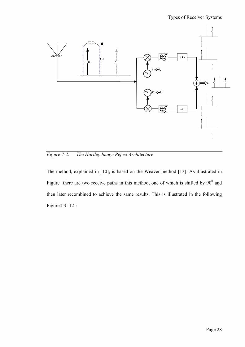
The method, explained in [10], is based on the Weaver method [13]. As illustrated in
Figure there are two receive paths in this method, one of which is shifted by 900 and
then later recombined to achieve the same results. This is illustrated in the following
Figure4-3 [12]:
Page 42
Types of Receiver Systems
Page 29
Figure4-3: The Weaver Image Reject Architecture
4.4 Direct Conversion Receivers
Figure 4-4: The Direct Conversion Receiver
Page 43
Types of Receiver Systems
Page 30
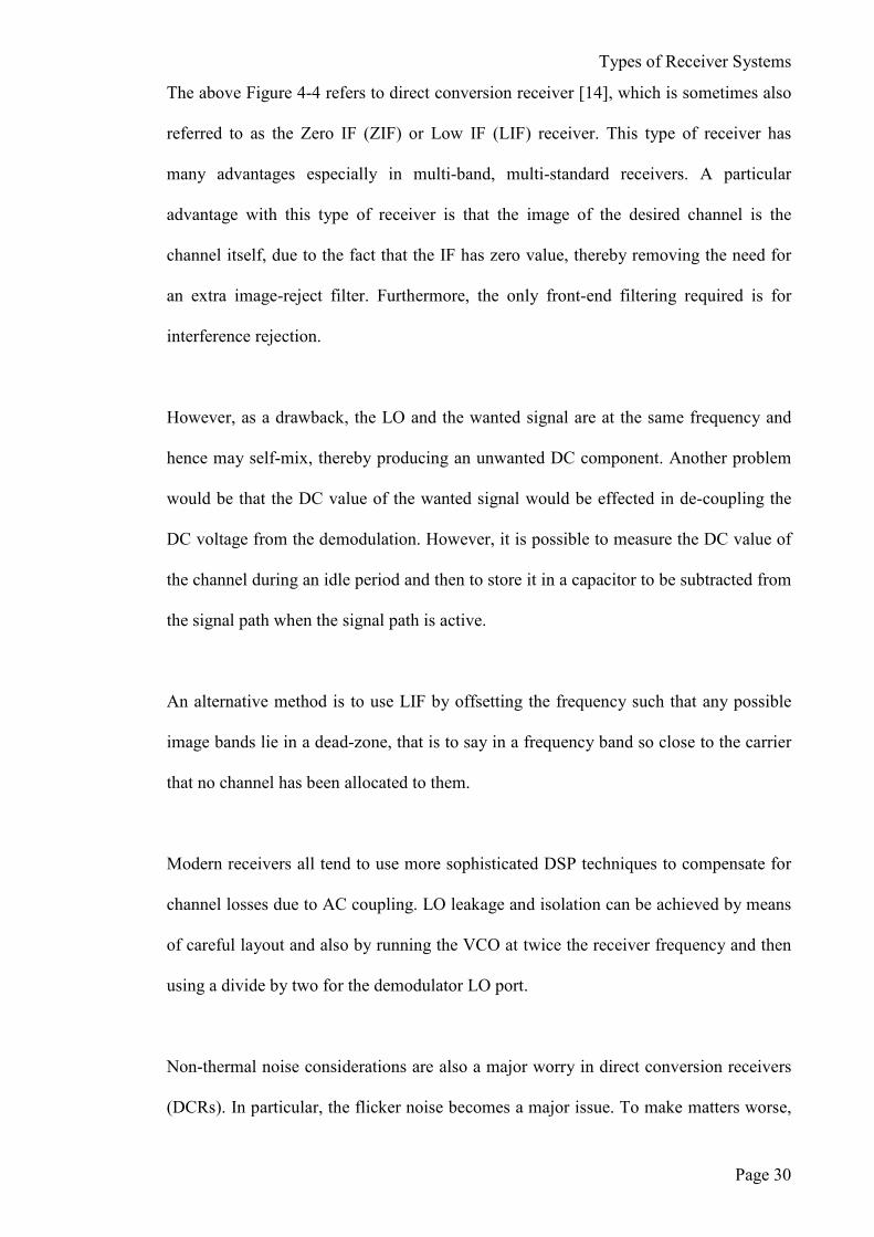
The above Figure 4-4 refers to direct conversion receiver [14], which is sometimes also
referred to as the Zero IF (ZIF) or Low IF (LIF) receiver. This type of receiver has
many advantages especially in multi-band, multi-standard receivers. A particular
advantage with this type of receiver is that the image of the desired channel is the
channel itself, due to the fact that the IF has zero value, thereby removing the need for
an extra image-reject filter. Furthermore, the only front-end filtering required is for
interference rejection.
However, as a drawback, the LO and the wanted signal are at the same frequency and
hence may self-mix, thereby producing an unwanted DC component. Another problem
would be that the DC value of the wanted signal would be effected in de-coupling the
DC voltage from the demodulation. However, it is possible to measure the DC value of
the channel during an idle period and then to store it in a capacitor to be subtracted from
the signal path when the signal path is active.
An alternative method is to use LIF by offsetting the frequency such that any possible
image bands lie in a dead-zone, that is to say in a frequency band so close to the carrier
that no channel has been allocated to them.
Modern receivers all tend to use more sophisticated DSP techniques to compensate for
channel losses due to AC coupling. LO leakage and isolation can be achieved by means
of careful layout and also by running the VCO at twice the receiver frequency and then
using a divide by two for the demodulator LO port.
Non-thermal noise considerations are also a major worry in direct conversion receivers
(DCRs). In particular, the flicker noise becomes a major issue. To make matters worse,
Page 44
Types of Receiver Systems
Page 31
CMOS mixers contribute far more heavily to flicker noise than bipolar technology does.
One way to reduce the flicker noise is to increase the device size thereby increasing the
gate capacitance, which ultimately reduces the flicker noise. However, by increasing the
effective capacitance the effective RF gain is reduced significantly due to the
decoupling effects of the junction capacitor.
For this reason, many of the current generation of DCRs are actually low-IF receivers,
whereby the IF is at 100 MHz rather than zero, and this is then processed using high-
speed DSP techniques. Newer techniques used in industry, especially for the low-signal
requirement transmission schemes such as Bluetooth, employ passive FET mixers that
do not contribute flicker noise. These mixers are being implemented currently by
companies such as NXP in their latest Bluetooth chipsets. However, the exploration of
this type of technology is beyond the scope of this present work.
4.5 Conclusion
Having considered the merits of various receiver architectures it is found that the direct
conversion architecture with LIF is best suited for the requirements of designing a
UMTS receiver chipset in CMOS technology. The image frequency issues associated
with LIF can be eliminated by making sure that the image band is in an unallocated part
of the spectrum, where no other transmission frequency has been allocated.
Page 45
Types of Receiver Systems
Page 32
4.6 References
[1] F.M Colebrook, “Homodyne,” Wireless World and Radio Rev., 13, 1924, p.774
[2] T.G. Tucker, “The Synchrodyne, “ Electronic Engineer, 19, March 1947, pp.
7576
[3] T.G.Tucker, “The History of Homodyne and Synchrodyne,” Journal of the
British Institution of Radio Engineers, April 1954.
[4] A.A. Abidi, “Direct-Conversion Radio Transceivers for Digital
Communications,” IEEE Journal of Solid State Circuits, Vol. 30, No. 12, December
1995
[5] Behzad Rezavi, “Design Considerations for Direct-Conversion Receivers,”
IEEE Transactions on Circuits and Systems-II: Analog and Digital Signal Processing ,
vol. 44, No.6, June 1997.
[6] S. J Franke, “ECE 353 Radio Communication Circuits, “ Department of
Electrical and Computer Engineering, University of Illinois, Urbana, IL, 1994
[7] B. Rezavi, “RF Microelectronics, “ Prentice Hall, Upper Saddle River, NJ, 1998.
[8] J. C. Rundell, et al., “Recent Developments in High Integration Multi-standard
CMOS Transceivers for Personal Communication Systems, “International Symposium
on Low Power Electronics and Design, 1998.
[9] Available online at http://www.info411.ece.mcgill.ca/411_notes/super-het.pdf
[10] J.C Rundell, “Issues in RFIC Design, “ Lecture Notes, University of California
Berkeley/National Technology University, 1997.
[11] R. Hartley, “Single-sideband Modulator, “U.S. Patent No. 1666206, April 1928.
[12] Nam-Soo Kim, Jung-Ki Choi, Shin-Chol Kim, Sang-Gug Lee, Chan-Gu Lee,
Hae-Won Jung, Hyun-Kyu Yu, “ An image rejection down conversion mixer
architecture”, IEEE
TENCON 2000. Proceedings Volume 1, 2000 pp 287 - 289 vol.1
Page 46
Types of Receiver Systems
Page 33
[13] D. K Weaver, “A Third Method of Generation and Detection of Single Sideband
Signals,” Proceedings of the IRE, Vol. 44, December 1956, pp. 17031705.
[14] Behzad Resavi, “ A 60 GHz Direct Conversion CMOS Receiver”, International
Solid States Circuits Conference, 2005.
Page 47
Page 34
5 Design Investigation
5.1 Introduction
In this chapter the principal receiver design requirement is defined against the
sensitivity requirement specified in the 3GPP requirements specification for UMTS
receivers for mobile handsets. Based on this requirement and the requirements defined
in chapter 3, 4 and 5, a suitable receiver circuit is designed an analysed, introducing
new and innovative methods the components and circuit in a performance limiting
technology such as the 0.35 µm CMOS Technology .
5.2 Sensitivity requirements for WCDMA Receivers
The ability of the receiver to receive radio frequency signal transmission depends on its
sensitivity. The receiver’s function therefore is to amplify the signal to a higher level so
that the detector circuit can detect and decode the signal whilst adding as little noise as
possible. The noise can be categorised as thermal noise, flicker noise and losses in
signal path. [1]
Thermal Noise Power = kT (25)
where k is Boltzman’s constant = 1.38 x 10⁻²³ JK
-1,
and T is room temperature in Kelvin = 290 K
Therefore thermal noise (in dB) = -203.9 dBW.
which in dBm is -203.9 + 10 log1000 =-174 dBm
Page 48
Design Investigation
Page 35
Channel bandwidth = 3.84 MHz which in dB is 65.843 dB, where the Channel
Bandwidth in the bandwidth of the modulated signal without the carrier present.
Thermal noise at the antenna is therefore = -174 + 65.8 dB = -108.2 dB
For the 12.2 kbps (for voice) WCDMA modulation scheme, the code length is 128 bits.
Therefore, the thermal noise is reduced by this amount due to the de-spread. In dB this
is 10 log (1/128) = 21.072 dB.
The effective noise power is therefore -108.2 – 21.1 = 129.3 dBm
For a 0.1 % BER, the required SNR (Es/No) is 0.9 dB
(Note: that for Eb/No this is 0.9 + 4, which is approximately 5 dB)
Therefore the required noise power at the antenna cannot be less than -128.4 dBm and
the WCDMA requirement is for -117 dBm
This translates to a maximum noise contribution in the receiver of -117 – (-128.4) =
11.4 dB. Allowing for a margin of error of 2 dB, the maximum noise contribution must
not exceed 9.4 dB in the receiver [2].
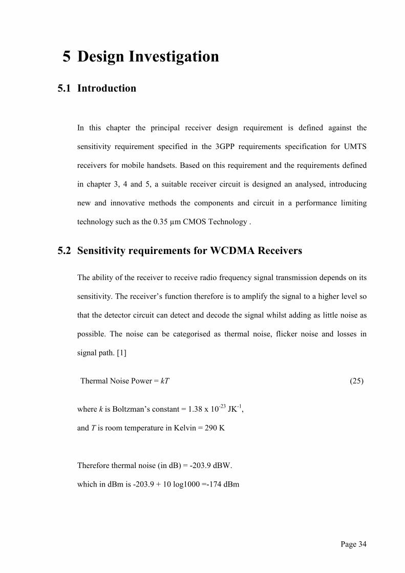
This is summarised in the following table:
Thermal Noise @290K -174 dBm/Hz
For Receive Band Noise 3.84 MHz 65.843 dB
Code De-Spread Noise Reduction For code length 128 bits -21.072 dB
Required SNR Eb/No (for voice channels) +5 dB
Margin of Error +2 dB
WCDMA Requirements For Hand Terminals -117 dBm
Allowed Maximum Receiver Noise 174-(65.8+21.1-5-2)-117 9.4 dB
Table 5-1: Systems Noise Budget for Receiver
Page 49
Design Investigation
Page 36
5.3 The LNA
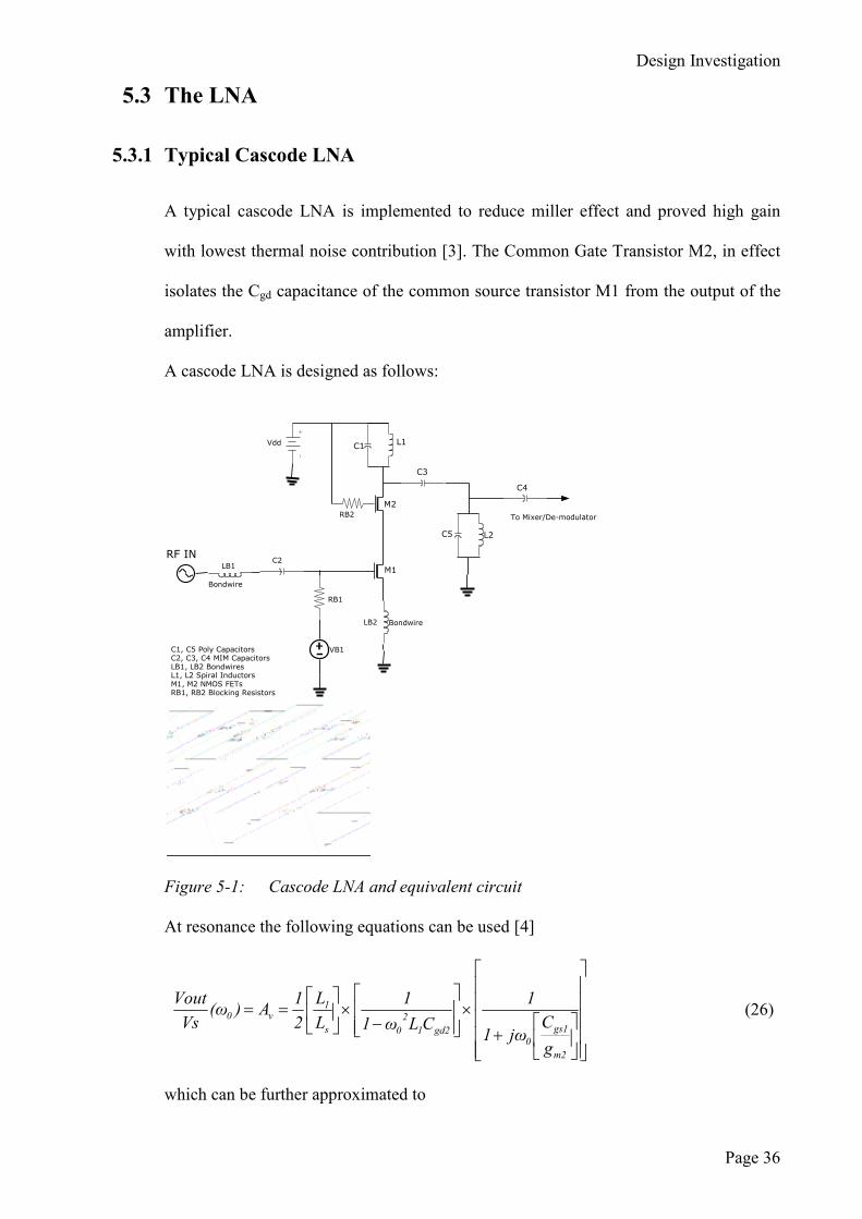
5.3.1 Typical Cascode LNA
A typical cascode LNA is implemented to reduce miller effect and proved high gain
with lowest thermal noise contribution [3]. The Common Gate Transistor M2, in effect
isolates the Cgd capacitance of the common source transistor M1 from the output of the
amplifier.
A cascode LNA is designed as follows:
_+
L1C1
M2
RF IN
Bondwire
Bondwire
M1
To Mixer/De-modulator
LB1C2
RB1
RB2
C3
C5 L2
LB2
Vdd
C1, C5 Poly CapacitorsC2, C3, C4 MIM CapacitorsLB1, LB2 BondwiresL1, L2 Spiral InductorsM1, M2 NMOS FETsRB1, RB2 Blocking Resistors
C4
VB1
Figure 5-1: Cascode LNA and equivalent circuit
At resonance the following equations can be used [4]
+
×
−×
==
m2
gs1
0gd21
2
0s
1v0
g
Cjω1
1
CLω1
1
L
L
2
1A)(ω
Vs
Vout (26)
which can be further approximated to
Page 50
Design Investigation
Page 37
+
×
≈
T
s
v
jL
LA
ωω0
1
1
1
2
1 (27)
and the Noise Figure can be calculated as
NF=
+Γ+
2
22
0411
mm
gs
gg
Cω (28)
The capacitive effects of the NMOS transistor is resonated out with the gate inductor
LB1 and the degenerative inductor LB2 provides the real impedance for the input match.
The load inductor L1 together with the load capacitor C1 provide the load at resonance
frequency.
The common gate transistor M2 is tied up to provide an open gate between the drain of
the first transistor M2 and the output of the amplifier. M1 is then biased to provide the
required gain.
5.3.2 Low biased cascode LNA with Drain Follower
The proposed LNA consist of a low biased cascode LNA stage consisting of high-
mobility NMOS devices and followed by a more linear but higher noise contributing
PMOS drain follower stage. This configuration is illustrated in the following diagram:
Page 51
Design Investigation
Page 38
_+
Figure 5-2: Low Biased Cascode LNA with Drain Follower
A number of improvements were made in the above circuit. They are as follows:
1. Input capacitance is added in parallel to the bond-wire inductance to provide higher
value inductances. This is further explained in the following Figure 5-3:
Figure 5-3: LNA Bondwire connection method
Bond-Wire
On-chip
capacitor
On-chip bond pad
Package pin pad
with no connection
Package pin pad with
connection
Page 52
Design Investigation
Page 39
The effect of this arrangement is that the effective Q of the component is increased by
reducing the resonance frequency near but not below the required frequency band. Thus
thicker bond-wires can be used, that have a lower overall inductance value but
significant also have a lower effective series resistance value as well.
2. The input cascode stage of the LNA is biased lightly, thus providing a low mg but
higher compression point [6]. This has the added effect of lowering the first stage noise
figure but also considerably lowering its gain.
3. The second stage LNA consisting of the Drain follower PMOS device, which provides
the vast majority of the gain and isolates the first stage LC parallel resonant load from
the output load requirements of the LNA.
The biasing at the input stage could further be explained as that of a “deep” class AB
design, lately being used as the preferred technique in modern Linear PA techniques,
but in this case it was utilised for the receiver LNA. By keeping the bias very low,
barely enough to switch the amplifier on, higher signal strengths were tolerated by the
LNA.
Designing this in two stages, used the low mobility stage PMOS transistor in the second
stage of the design. Even though this second stage had a high NF, this effect was
reduced by the first stage amplification.
Page 53
Design Investigation
Page 40
5.3.3 Balanced Lightly Biased Cascode LNA with Drain Follower
This is the same as the single-ended version of the LNA but is balanced at the input.
This method is explored in order to utilise a single component balanced filter at the
input, rather than having to implement a Balun at the stage following the LNA.
Balanced inputs are required as the de-modulator is an image reject double balanced
Gilbert cell type circuit. Such a configuration is required as this design is that of a Low-
IF configuration rather than that of a Zero-IF, and hence image rejection is a real and
serious issue.
5.4 The Mixer (De-Modulator) Circuit
The down-conversion mixer is a quadrature Gilbert-type direct conversion mixer and is
designed as shown in the following Figure 5-4.
_
+
Figure 5-4: Quadrature Image Reject Mixer/ Demodulator
As can be seen from the above diagram, the image reject mixer consists of 8 switching
transistors and 4 transconductors, all arranged in symmetry. One pair of switching
transistors and a transconductor constitutes a single balanced mixer. For analytical
purposes, the following diagram is that of one such balanced mixer.
Page 54
Design Investigation
Page 41
Each differential input to the mixer has a transconductor stage and this consists of a
single NMOS device. The functionality of the transconductor is to convert the available
voltage into current to be mixed by the upper section of the switches, operated at the LO
frequency.
The upper switching section of the mixer is controlled both by a gate bias and by the LO
signal at its input. The applied gate bias thus acts as an offset voltage to the mixing
action of the circuit. Sharp transitions in the LO signal provide a better zero crossing
noise contribution and nonlinearity.
Flicker nose is contributed by two mechanisms [5]:
1. Zero crossing of the tail current (the direct method).
2. Induced current in the tail capacitance (the indirect method).
Larger capacitive gates and floating on-chip inductors tend to reduce the flicker noise as
they filter out some of the noise [6]. The width of the transistor has been set to 1.5 mm,
which is the recommended width for optimum TF from the graph in Figure (appendix
section). The benefit of the floating inductor method described in [6] remains doubtful
as simulations tended to show little or no benefit when implemented in the mixer
circuit.
The widths of all the transistors are for maximum TF (or Tω )and hence minimum NF as
illustrated in the following equation [7]:
2
min
2.1 2. .[ ] 1 . (1 )
5n opt c
T
F R G G cω
γ δω
= + + ≈ + − (29)
where
2. .T Ftω π= (30)
Page 55
Design Investigation
Page 42
and γ is the body coefficient, δ the gate noise coefficient and c the correlation
coefficient.
Due to the direct conversion requirements placed on these mixers, reactive components
at frequencies close to zero are not possible, and active loads would provide excessive
noise. For these reasons, resistive loads are placed, even though they consume valuable
voltage headroom.
5.5 The Capacitor
In the CMOS 35 µm AustriamicrosystemsTM
process there are two main types of
capacitors available. One is the Poly1-Poly2 capacitor and the other is the Metal to
Metal capacitor also know as the Metal Insulator Metal (MIM) capacitor. The Poly1-
Poly2 capacitor has a higher variation of +11% to -9%, which has to be taken into
account in the matching circuit. In most cases it was found more prudent to use these
poly capacitors only for de-coupling and coupling requirements as the capacitance per
unit area was much greater than the MIM variety. The ESR value was also much larger
in Poly-Poly capacitors, with component Q of 54 at 1 pF and 13.5 at 4 pF at a frequency
of 2.14 GHz [8].
The MIM capacitor is highly tolerant to process and temperature variations. With a
capacitance range of 0.1 pF to 1 pF, it has a tolerance of better that 5% over all PVT
variations. The minimum component Q factor of this device is 100 [8].
5.6 The Resistor
Poly resistors and high poly resistors were both used. Poly resistors tended to have
greater accuracy and were therefore used accordingly. In addition N-well resistors were
Page 56
Design Investigation
Page 43
also used for biasing circuits where the signal had to be prevented from entering the DC
bias domain.
The frequency response of these resistors is consistently far above 6 GHz [8]. Since the
actual high frequency response of these devices is approximately constant, further
explanation is deemed unnecessary.
5.7 The Inductor
The accuracy of an inductor model is extremely important in RF circuit matching, as it
determines the performance of the whole circuit. In blocking applications, the effective
series resistance of the inductor creates an effective voltage drop that limits the overall
voltage swing.
Warren and Fordemwalt [9] proved in 1965 that planar inductors cannot be used for IC
design. However, Nyugen and Meyer [10] published in 1990 the use of planar
inductors, which have been used extensively in IC design. However, these early
inductors had extremely low Q values, with [11] achieving a Q value of just 3 at 1GHz
for a 9.7 nH inductor.
Since then, thicker metals with low series resistance and much higher substrate
resistances have been developed. The model developed by [12] achieved a Q of 12 for a
2.88 nH inductor at 3 GHz, with metal thickness of 14 µm, spacing of 4 µm and with
only two turns. The area needed for these inductors is obviously very high in terms of
silicon real estate.
The general conclusion of this investigation was that the fewer the number of turns, the
larger the inner diameter and the thicker the metal, then the better the Q and hence the
ESR value of the device. However, until [13] in 1996, previous models have all been
mostly based on numerical and curve fitting methodologies. The model described in
[13] is as follows:
Page 57
Design Investigation
Page 44
Figure 5-5: Spiral Inductor and its Parasitic Model
−+ ++= effeffeff MMLL (31)
where effL is the self-inductance of the coil and +effM is the positive mutual inductance
and −effM is the negative effect of the mutual inductances.
From this
+++
+=
l
tw
tw
llLeff
35.0
2ln2 (32)
where w is the wire width, t the wire thickness, and l the wire length all in cm and Leff is
in nH.
The Mutual inductance is given as
M=2.Qm.l (33)
where Qm is the mutual inductance parameter, calculated from the equation
2 2 2 2ln( / ) 1 ( / ) 1 ( / ) ( / )mQ l GMD l GMD GMD l GMD l= + + − + + (34)
GMD is the Geometric Mean Distance between the two conductors and is calculated
from the equation,
2 4 6
8 10
ln ln [1/12.( / ) ] [1/ 60.( / ) ] [1/168( / ) ]
[1/ 360( / ) ] [1/ 660( / ) ......
GMD s s w s w s w
s w s w
= − + + +
+ + (35)
where w is the width and s the separation space in cm
L
Rs
Cp
Cox
CsRs1
Cox
CsRs1
Page 58
Design Investigation
Page 45
Rs=efftw
l
.
.ρ (36)
where )1.( /δδ t
eff et −−= (37)
and f..µπ
ρδ = (38)
where efft is the effective metal thickness and δ the skin depth of the metal and µ is the
permeability of the metal . Since the thickness of the metal is fixed by the process, the
effective thickness can be obtained from the measured values given in the process
manual [14].
2
1 2
. oxp
oxM M
C n wt
ε
−
= (39)
where 1 2oxM Mt − is the oxide thickness between the spiral and the underpass and n the
number of turns.
ox
ox
oxt
wlCε..
2
1= (40)
where Cox represents the oxide capacitance
The substrate capacitance and resistance are derived as
subsi CwlC ..2
1= (41)
and sub
siGwl
R..
2= (42)
where Csub and Gsub are the substrate capacitance and conductance per unit area
Ignoring the effects of Csi, Rsi and Cox, a table can be prepared of the approximate values
of all inductors prior to final simulation.
Page 59
Design Investigation
Page 46
Rs can be obtained from the process manual [15] which lists RMETT, the thick, top
level metal as having a 10 mΩ per square as typical value.
pC can also be obtained from the process manual [15] for layer 4 thick metal, which is
0.099 fF/µm.
Tmett (typical) is 2.8mm for the typical thickness of the thick metal layer used to make
spiral inductors in the Austria Micro Systems CMOS C35 process [15].
The component Quality Factor of the inductor can be estimated from the equation
S
L
R
XQ = (43)
and the resonance frequency is
CLf res
.2
1
π= (44)
From the RF Spice models data sheet, one can select an appropriate inductor based on
initial simulation of the circuit. As can be seen from the above results, there remain
discrepancies in the parallel capacitor value and in the inductance value. The calculated
inductance just about tallies with the inductance value from simulation, with the slight
discrepancies being attributed to the extra lead wires in and out of the inductor and in
the metal 3 layer.
It is difficult to quantify the source of the extra capacitances in the simulations, but this
is probably due to the N-well in which the inductor sits.
Page 60
Design Investigation
Page 47
5.7.1 More accurate analysis of the inductor
Ignoring the substrate capacitor and resistor, and also the oxide capacitor, and based on
the formulae above, the appropriate values can be calculated. The process data sheet
was used to obtain the process parameters. The results are shown in the following table:
Total metal area (m2) 3.99E-08
Cp (pF) 3.68E-01
Rs (Ω) 6.23E+00
Outer Diameter, D (cm) 2.50E-02
Width, w (cm) 8.00E-04
Space, s (cm) 8.00E-04
Effective Thickness, Teff (cm) 2.80E-06
Inner Diameter (cm) 6.60E-03
Total Length (m) 4.99E-03
Total Length (cm) 4.99E-01
Resonance Frequency, fres (GHz) 4.38E+09
Leff (nH) 3.58E+00
M+ Eff (total) in nH 7.23E-03
M- Eff (total) in nH -3.62E-03
Q at fo 8.67E+00
fo (GHz) Operational Frequency 2.40E+00
Total inductance (nH) 3.59E+00
Table 5-2: Calculated Inductor values
A comparison table between simulated and calculated results follows:
L Rs Cp [email protected] GHz S.R.F
Calculated 3.6nH 6.4 0.21pF 8.7 5.7 GHz
Actual 3.8nH 6.4 0.12pF 9.0 >6GHz
Table 5-3: Inductor Comparison table
As seen in Table 5-3, there is agreement between the calculated and simulated values, in
spite of ignoring some of the less significant parasitic effects.
The thickness and space of the 4 ring square inductor on thick metal layer 4 was
calculated as shown in Table 4. The width and spacing between the spirals was 8 µm
Page 61
Design Investigation
Page 48
and the outer diameter was 250 µm, and we can calculate that the inner diameter was 66
µm in width. The smaller inner diameter has a negative impact on the overall inductance
of the device as this introduces more coupling between opposite inductive fluxes, so
reducing the overall mutual inductance value.
However, decreasing the width of the conductor will increase the Effective Series
Resistance (ESR) and consequently the Q factor of the component. The thickness and
width of the tracks is usually a good indication of the resistance per unit length of the
transmission line that is wound up to make the inductor. Therefore, the thicker the metal
layer and the wider it is, the better in reducing the ESR and increasing Q.
However, this causes an increase in the size of the inductors as mentioned earlier, and
so the area they require. Since for each process there is a limit on the amount of metal
that can be laid on top of the substrate without causing mechanical deformation to the
oxide layers, large sized inductors can thus be a problem. Increasing the width also
reduces the self-inductance of the transmission line itself, requiring an even greater
length of line to be used, which in turn increases the overall ESR of the component.
A number of studies have therefore concentrated on methods of maintaining maximum
conductor width and diameter [16] at the cost of reducing the inner diameter of the
conductor. Methods to offset the effects of negative mutual inductance vary from
patterned centre areas [17] to various combinations of active and passive dopants [18]
and oxides. None of these appears to have had a significant effect except of course for
the general method of laying out the whole inductor in an N-well thus reducing
substrate currents.
Page 62
Design Investigation
Page 49
These then are the perennial problems with spiral inductor designs, as they occupy areas
that are far greater than any other component in a RF circuit. Often this implies an area
of up to 70% of the total die area. To keep this area to a minimum, without reducing the
performance, is quite crucial.
Figure 5-6: Positive Mutual Inductance
In a 4 turn rectangular spiral inductor, there are typically 17 segments of transmission
line. For the purposes of calculating the mutual inductances, each line segment is treated
separately. The magnetic flux coupled between the two is calculated for the smaller of
the two segments, to include every segment in parallel. This then is varied for each
segment incrementally to include all segments of each turn. It should be noted that
magnetic fluxes do not couple in a perpendicular plane to each other, so giving no
contribution.
As can be seen from the plots in Figures 5-6, the further the inductor is wound the less
the mutual inductance contribution becomes per sector, the contribution of the last
sector providing the least mutual inductance value. The overall contribution to the total
Positive Mutual Inductances
5.00E-05
7.00E-05
9.00E-05
1.10E-04
1.30E-04
1.50E-04
1.70E-04
1.90E-04
2.10E-04
2.30E-04
0 2 4 6 8 10 12 14 16
Segment Number
Ind
uc
tan
ce
(n
H)
M+4
M+8
M+12
M+16
Page 63
Design Investigation
Page 50
inductance is still small when compared to the self-inductance of the inductor coil. The
overall negative mutual inductance contribution can be seen to contribute an even
smaller amount of negative inductance to the overall inductor value using the 4 inductor
arrangement chosen here and especially with a larger inner diameter of the coil.
The thinner a piece of wire, the more magnetic flux is available external to that piece of
wire, as there is less skin depth [19]. However, this is at the cost of higher resistivity
and hence lower Q factor and can be deduced from equations 33 and 40.
A new method of introducing a parallel capacitor to the classical inductor equivalent
circuit, described in [20], reduces the inductor’s Self Resonant Frequency (SRF). The
closer the SRF of the inductor to the frequency of operation, the more responsive are its
impedance characteristics.
However, in altering the SRF the bandwidth of operation is also reduced considerably.
In a narrow-banded system such as UMTS, where there is 60 MHz bandwidth in each
direction, such a technique is deemed appropriate, indeed advantageous.
6.6.1.1 Introducing a parallel capacitor to the inductor
The reactance of an inductor can be increased if it is made to resonate with a capacitor
in parallel.
LjX L ω= (45)
Cj
XC..
1
ω= (46)
Page 64
Design Investigation
Page 51
where LX and CX are the reactance of an inductor and capacitor respectively.
However, in parallel, the total impedance of the circuit is CL XXZ //= which implies
that
2
. .
1 . .
j LZ
LC
ωω
=−
(47)
Theoretically, the impedance can therefore be infinite at resonance, obviously the point
at which the frequency is such that CL..1 2ω− is equal to zero. Obviously, in real
circuits the parasitic effects will always prevent this from becoming zero. This is best
illustrated in the following Figure 7:
Figure 5-7: Parallel Resonance Graph
This then is a useful circuit to implement, especially when the RF energy needs to be
isolated from the DC power supply and so forth. The danger is that outside the
frequency of resonance, the impedance drops and therefore is applicable in narrow-band
circuits only. Fortunately, the UMTS system for which the circuit was implemented has
a bandwidth of 60 MHz, which then implies a Q of 40 at 2.14 GHz.
6.00E+01
1.10E+02
1.60E+02
2.10E+02
2.60E+02
0.E+00
5.E+15
1.E+16
2.E+16
2.E+16
3.E+16
3.E+16
4.E+16
4.E+16
5.E+16
5.E+16
5.E+00 6.E+00 7.E+00 8.E+00 9.E+00
Imp
ed
an
ce
(Ω)
for
L v
s Z
cu
rve
Imp
ed
an
ce
(Ω f
or
L/C
vs
Z c
urv
e)
Inductance (nH)
(L//C) vs Z
L vs Z
Page 65
Design Investigation
Page 52
Maximum power transfer and a low noise figure are prerequisite for an LNA and to
achieve these, a good impedance match with the least amount of ESR is important is
important. In the case of narrow band systems, a large inductor can be reduced further
by using the described parallel capacitor method. In on-chip spiral inductors, this
provides a significant improvement in the reactiveness of the inductor together with a
significant reduction in size.
The graph in Figure 5-7 illustrates this well, showing that even a small capacitor in
parallel to the inductor provides an enormous improvement in the reactiveness of that
inductor.
Figure 5-8: Improvements in "Q" at Resonance with a parallel C with the L
In the graph in Figure 5-8, the inductor has been set to 6 nH and the capacitor is varied
from 0.1 pF to 1.3 pF. From this graph, the improvements in impedance transformation
are obvious. The advantage is that lower value inductors can thus be implemented at the
-1.E+03
-5.E+02
0.E+00
5.E+02
1.E+03
2.E+03
2.E+03
3.E+03
0.E+00 5.E-01 1.E+00 2.E+00
Imp
ed
an
ce
(Ω )
Parallel Capacitor (pF)
Improvements in Circuit Reactance
Inductor Impedance
parallel resonator
Page 66
Design Investigation
Page 53
cost of an additional capacitor. Given the typical area required by a MIM capacitor, at
around 1 pF, this is minimal when compared to an inductor of any value. The method is
thus extremely valuable in obtaining significantly better results.
5.8 Conclusion
The maximum receiver noise contribution is calculated to be 9.4 dB, based on the 3GPP
receiver sensitivity requirement. Based on this a cascode LNA with a drain follower is
introduced in a novel way. The LNA is designed to provide better signal tolerance to the
transceivers own transmission signal, whilst maintaining the overall signal amplification
and noise contribution. The value and size of the inductor at the input of the LNA is
minimized by using the well understood parallel resonance method but in a novel way
as part of the input match.
Page 67
Design Investigation
Page 54
5.9 References
[1] RF Design Guide, Peter Vizmuller, 1st Edition, Artech House, pp. 14, 1995.
[2] O. K. Jensen, T. E. Kolding, Chris. R. Iversen, S. Laursen, R. V. Reynisson, J.
H. Mikkelsen, E. Pedersen, M. B. Jenner, and T. Larsen,, "RF Receiver Requirements
for 3G WCDMA Mobile Equipment", Microwave Journal, 2000, vol. 43, no. 2, pp. 22-
46.
[3] The Design of CMOS Radio-Frequency Integrated Circuits, Thomas H Lee. 2nd
Edition, Cambridge University Press, pp. 248, 2004.
[4] The VLSI Handbook, Ed Wai-Kai Chen, Boca-Roton: CRC Press, LLC 2000,
(ISBN 0-8493-8593-8) pp. 659-661, 1990.
[5] H.Darabi and A.A. Abidi, “Noise in RF-CMOS mixers: A simple physical
model,” IEEE J. Solid-State Circuits, vol. 35, pp. 1528 – 1545, Oct. 2000.
[6] H. Sjoland, A.Karim-Sanjaani, “A Merged CMOS LNA and Mixer for a
WCDMA Receiver,” IEEE J. Solid-State Circuits, vol. 38, pp. 1045-1050, June 2003.
[7] The Design of CMOS Radio-Frequency Integrated Circuits, Thomas H Lee. 2nd
Edition, Cambridge University Press, pp. 369, 2004.
[8] Austria Micro Systems: “0.35 um CMOS C35 RF SPICE Models”, Rev.4, pp.
24-27, http://www.austriamicrosystems.com/
[9] R.M.Warner and J.N Fordemwalt, Eds., Integrated Circuits, Design Principles
abd Fabrication. New York: McGraw-Hill, 1965, p.267.
[10] N.M. Nguyen and R.G.Meyer, “Si IC-compatible inductors and LC passive
filters,” IEEE J. Solid-State Circuits, vol. 25, no. 4, pp. 1028-1031, Aug. 1990.
[11] D. Lovelace, N. Camilleri, and G. Kannell, “ Silicon MMIC inductor modelling
for high volume, low cost applications,” Microwave J., pp.62-71, Aug. 1994
Page 68
Design Investigation
Page 55
[12] K.B. Ashby, I.A. Koullias, W.C. Fineley, J.J. Bastek and Shahriar Moinian,
“High Q Inductors for Wireless Applications in a Complementary Silicon Bipolar
Process,” IEEE J. Solid-State Circuits, VOL. 31, no.1,pp. 4-8, Jan. 1996.
[13] C.P.Yue et l., “ A Physical Model for Planar Spiral Inductors on Silicon,” IEDM
Tech. Dig., 1996, pp. 155-158.
[14] AustriamicrosystemsTM
Process Manual, ENG-182 rev4, pp 28. Available online
at www.Austriamicrosystems.com.
[15] AustriamicrosystemsTM
Process Manual, ENG-182 rev4, pp 38 - 39. Available
online www. Austriamicrosystems.com.
[16] Craninckx.J. and Steyaert. M, “ A 1.8 GHz low-phase-noise CMOS VCO using
optimized hollow spiral inductors,” IEEE J. Solid-State Circuits, vol. 32, No. 5, 1997,
pp 736-745.
[17] Yue, C.P, and Wong S.S., “On-chip spiral inductors with patterned ground
shields for Si-based RF IC’s,” IEEE J. Solid-State Circuits, vol. 33, No. 5, 1998, pp
743 – 752.
[18] Mernyei F, Darrer. F, Pardoen. M and Sibrai. A, “Reducing the substrate losses
of RF integrated inductors,” IEEE Microwave and Guided Wave Letters., vol. 8, No 9,
1998, pp 300- 301.
[19] Dylan Kelly, Frank Wright, “Improvements to Performance of Spiral Inductors
on Insulators,” IEEE MTT-S Digest, pp. 541-543, 2002.
[20] Patric Yue and Simon Wong, “Physical modelling of spiral inductors on
silicon,” IEEE .J Solid-State Circuits, vol.47, No. 3, March 2000, pp 560 - 568.
Page 69
6 Analysis of the High Compression Point
LNA
6.1 Initial Simulation and Analysis of High Compression Point
LNA
A compression point of up to 10 dB better than comparable designs, without
significantly degrading the NF or the gain, was achieved in this project
As will be demonstrated in Table 6
case P1dB of -14 dBm at the input have been simulated for a gain of over 17 dB and a
NF of just over 2.6 dB, all using the relatively older 0.35 µm 4
technology.
Figure 6-1: P1dB Compression Curve for
Analysis of the High Compression Point
imulation and Analysis of High Compression Point
A compression point of up to 10 dB better than comparable designs, without
significantly degrading the NF or the gain, was achieved in this project
As will be demonstrated in Table 6-1, a single-ended common mode LNA with a worst
14 dBm at the input have been simulated for a gain of over 17 dB and a
NF of just over 2.6 dB, all using the relatively older 0.35 µm 4
P1dB Compression Curve for LNA
Page 56
Analysis of the High Compression Point
imulation and Analysis of High Compression Point
A compression point of up to 10 dB better than comparable designs, without
significantly degrading the NF or the gain, was achieved in this project (Figure 6-1).
ended common mode LNA with a worst
14 dBm at the input have been simulated for a gain of over 17 dB and a
NF of just over 2.6 dB, all using the relatively older 0.35 µm 4-metal CMOS
Page 70
Analysis of the High Compression Point LNA
Page 57
From [1] and [2] the maximum signal at the input is -25 dBm at the low gain setting and
-43 dBm at the high gain setting.
However, W-CDMA is a full-duplex system with a maximum PA output power of 29
dBm, which will find its way to the receiver. An LNA filter therefore has to attenuate
the transmitter signal by at least 43 + 29 = 72 dB, when operating the LNA at the
prescribed -43 dBm, in order to prevent the LNA from being compressed by the
transmitter signal..
Filter that produces 72 dB of attenuation of the transmission signal will inevitable
require a considerable amount of poles, which in turn would imply that the wanted
frequency band itself will be subjected to losses due to this filtering process.
By improving the linearity of the receiver path and in particular the LNA, it is possible
to implement a low loss filter with few poles and thereby increase the sensitivity of the
receiver.
By considering a highly linear LNA, with an input P1dB of -14 dBm or better, this
filtering requirement can be relaxed to the extent that the only filtering required will be
that provided by the front-end duplexer, thereby substantially reducing the receiver path
losses and also reducing the component count for the receiver.
Minimum Typical Maximum
PA Output Power 24 dBm 27 dBm 29 dBm
Duplexer Filtering -50 dB
Crest Factor 8.6 dB
Total -14.4 dBm
Table 6-1 Maximum Transmitter Signal at LNA input
Page 71
Analysis of the High Compression Point LNA
Page 58
6.2 The method of achieving the increased compression point
The P1dB is achieved by utilising a cascode structure and a folded drain follower. The
cascode amplifier is biased to a low current value, and at the point of saturation. This
lowers the mg value but also provides a greater tolerance to the incoming signal. For
large input signal values the bias itself is altered by the RF signal, in much the same
way as a Class B or Class AB Power Amplifier would do.
However, in Power Amplifier technology, this method is used to improve the efficiency
of the amplifier, but here we are using a similar method to get a better compression
point for the LNA, in order to make it more tolerant of larger Transmitter Signal feed-
through.
The consequence of a smaller mg , due to the above mentioned method, means that the
gain is also smaller. This gain is then boosted by having a PMOS device as a second
stage amplifier. This 2nd stage amplifier designed with a PMOS device means that there
is:
1. Isolation between 1st stage load and mixer/de-modulator load.
2. Maximum load impedance LR for 1st stage cascode amplifier as Lmv RgA = .
3. PMOS device hole mobility is typically ¼ of the electron mobility of the NMOS
device, but has a much larger Thermal Noise effect.
4. Total Noise effects of PMOS device is reduced by the previous stage NMOS
Cascode device.
The channel length modulation for small signals can be equated to a small resistor of
value or [3],
Page 72
Analysis of the High Compression Point LNA
Page 59
where DSGS
DS
oIV
Vr
λδδ 1
≈= (48)
and L
L∆=λ (49)
and also LLL ′−=∆ (50)
where L is the stated length of the channel and 'L the effective length of the channel.
When VGS is decreased, then DSV in effect increases across the Common Source device.
This in turn increases the value of or , effectively increasing the value of the signal that
the amplifier can accept.
The transconductance mg [3] can similarly be equated as
DS
GS
GS
Dm
V
V
V
Ig
δδ
δδ
*= (51)
Page 73
Analysis of the High Compression Point LNA
Page 60
Figure 6-2: LNA Equivalent Circuit of the 1st stage (Cascode)
From Figure 6-2, shunning the current re-use arrangement as is traditionally applied in
most designs, and biasing the telescopic first stage cascode structure with a low current,
provides a sufficient voltage gain. The input stage has a large voltage DSV across the
drain and the source terminals due to the small gate voltage. This provides a large
voltage gain.
Note that though the gate voltage is small, the channel is not fully depleted of holes, and
therefore the conductivity of the channel is reduced. This then enables higher signals to
be present at the gate. In other words, equation (51) can be re-written as:
GS
Dm
V
Ig
δδ .
= (52)
Page 74
Analysis of the High Compression Point LNA
Page 61
which implies that the transconductance is low.
However,
D
DS
I
Vr
δδ
=0 (53)
indicating a large resistance [ohms law].
For the cascode structure to remain in saturation, the following conditions have to be
met:
At DSV almost 2 volts and DI just over 1mA for the first stage cascode amplifier 0r is
quite large in value. However, Av is large since DSV is large when compared to the
input voltage of 0.65 volts.
_+
_+
Figure 6-3 Drain Follower with equivalent AC circuit
The drain follower in Figure 6-3, which is the second stage of the LNA, provides the
common gate part of the cascode amplifier in Figure , with a very large impedance, due
Page 75
Analysis of the High Compression Point LNA
Page 62
to the fact that the parallel resonant LC structure is also of high impedance. Therefore,
there is a good inter-stage matching between the two sections of the LNA circuit. From
the schematic diagram in Figure 6-4:
M1: 1thinX VVV −≥ Since 1thV is around 0.6 volts and inV is only marginally greater, at
0.65 volts where Vx is the drain source voltage of the common source stage of the
cascode.
For each transistor to be in the saturation region, the drain source voltage has to be
greater than the difference between the gate voltage and the threshold voltage of the
gate.
Since 2GSbx VVV −= , we can conclude that in the LNA circuit M1 is in saturation as
2GSV is tied to the top voltage rail at 2.7 volts.
Now for M2 to also be in the saturation region, 2thbxout VVVV −≥− which can be
expanded to xthGSthinout VVVVVV +−+−≥ )()( 221 .
Therefore, for the LNA cascode section to be in saturation the above conditions have to
be satisfied. From initial DC simulations the following are the values obtain:
1 2th thV V= 0.56V
bV 2.7V
2DSV 0.69V
1DSV 1.98V
outV 2.7V
inV 0.65V
Table 6-2: LNA Bias Voltages
Page 76
Analysis of the High Compression Point LNA
Page 63
From the above values it is clear that M1 is in the saturation region since Vx, which is
in effect vVDS 98.11 = , much greater than 1thin VV − =0.05 volts
Also, M2 is in the saturation region since 2thbout VVV −≥ = 2.7 volts, which is greater
than 2.1 volts
Figure 6-4: Schematic Diagram of LNA i/p Circuit
By providing a lower mobility PMOS device as a second stage “drain follower” with
maximum current gain, it is then possible to provide a better overall gain in terms of
both voltage and current, i.e. power, at the output of the LNA. The lower hole mobility
of the PMOS device produces a better compression point for the second stage.
Page 77
Analysis of the High Compression Point LNA
Page 64
The lower hole mobility of the PMOS device does produce a larger noise contribution.
However, since the PMOS is a second stage device, its overall effect on the noise figure
is considerably restricted.
Page 78
Analysis of the High Compression Point LNA
Page 65
6.3 References
[1] The 3 GPP UMTS Standard [online]. Available: http://www.3gpp.org
[2] O. K. Jensen, T. E. Kolding, Chris. R. Iversen, S. Laursen, R. V. Reynisson, J.
H. Mikkelsen, E. Pedersen, M. B. Jenner, and T. Larsen,, "RF Receiver Requirements
for 3G WCDMA Mobile Equipment", Microwave Journal, 2000, vol. 43, No. 2, pp. 22-
46.
[3] Design of Analog CMOS Integrated Circuits, Behzad Razavi, McGraw-Hill
International Edition, pp 21-28, 2001.
Page 79
Page 66
7 Design and Simulation of the LNA
Three different types of LNA discussed in this section, together with the relevant design
and simulation results. All the results were performed by matching the input and output
ports to 50 Ω and 200 Ω respectively.
However, in the final implementation of the complete receiver discussed in Chapter 10,
output port of the LNA was left unmatched, but the input port of the mixer/de-modulator
was conjugately matched to the unmatched LNA port, thus providing optimum coupling of
signal between the two circuits, including “ideal” Balun circuits were relevant.
Page 80
Figure 7-1: Single Section of the Balanced LNA Cadence Schematic Entry
Design and Simulation of the LNA
Single Section of the Balanced LNA Cadence Schematic Entry
Design and Simulation of the LNA
Page 67
Single Section of the Balanced LNA Cadence Schematic Entry
Page 81
Design and Simulation of the LNA
Page 68
The circled section in Figure 7-1 shows the output matching for a 200 ohm load. In the
final systems implementation the input of the mixer is conjugately matched to the
unmatched output of the LNA. This is illustrated in the following Figure:
Figure 7-2: Conjugate Plot of LNA Output and Mixer Input
In Figure 7-2 the S22 port reflection coefficient and S33 port reflection coefficient
represent the LNA output and Mixer input port values respectively.
7.1 Typical Cascode LNA
A typical cascode LNA is designed as described in section 5.3.1.2 and Figure 5-1, but with
the cascode LNA itself being biased to provide all the required gain. The following
simulation results were performed at ambient temperature, using true models from the
AustriamicrosystemsTM
PDK. These include equivalent circuits for the bondwires and pads
and extracted layout parasitics.
Page 82
Design and Simulation of the LNA
Page 69
Variations to process, voltage and temperature were added to the simulations for final
verification of the design. However, all simulation data presented in this report considers
only typical values.
7.1.1 Input and output return losses
Figure 7-3: Typical Cascode LNA Input and Output Port Voltage Reflection
Coefficients
The input and output port voltage reflection coefficients are shown in Figure 7-3. The input
impedance is matched to 50 Ω and the output impedance is matched to 200 Ω. The output
matching is almost purely resistive and can be deduced from the narrow spread of the S22
value, indicated in red.
Page 83
Design and Simulation of the LNA
Page 70
Figure 7-4: Typical Cascode LNA Return losses (log magnitude)
The log magnitude graph above in Figure 7-4 provides the same results of that obtained in
the smith chart plot of Figure 7-3, but with more quantifiable values for the return losses.
As can be noted, the input return loss is below 18 dB across the frequency band of interest
and the output return loss is significantly below 50 dB.
Since the simulations were not performed with substrate analysis, these values are most
likely to be slightly worse, but nonetheless comfortably with the specification
requirements.
7.1.2 LNA Forward Gain
The forward gain of the LNA is simulated with a 50 ohm reference impedance at the input
and a 200 Ω reference impedance at the output. The supply voltage is set at 2.7 volts DC
and the input port power is set to -40 dBm. The typical gain at room temperature is shown
in Figure 7-5:
Page 84
Design and Simulation of the LNA
Page 71
Figure 7-5: Typical Cascode LNA Forward Gain
As can be seen from the Figure 7-5, the gain maintains a flatness of 17.5 dB over the
frequency of interest and displays very little ripple.
7.1.3 LNA Noise Figure
Page 85
Design and Simulation of the LNA
Page 72
Figure7-6: Typical Cascode LNA Noise Figure
As can be seen in Figure 7-6, the noise figure maintains a value of between 1.78 and 1.76
dB over the frequency of interest, which is virtually flat.
7.1.4 LNA 1 dB Compression Point
The Input P1dBm of the LNA is illustrated is simulated to obtain the linearity of the LNA
and is simulated with the supply voltage set to 2.7 volts and the temperature set to typical
at 27 oC. The following simulation result in figure indicates this linearity by means of the
P1dBm simulation shown in following Figure 7-7:
Figure 7-7: Typical Cascode LNA Compression Point Plot
As can be seen from the above Figure 7-7, the input P1dBm is at -25.1 dBm. This indicates
the maximum signal that can be tolerated by the LNA.
Page 86
7.1.5 LNA Current Consumption
Figure 7-8: DC Current Vs Input Power
As can be seen from
maximum uncompressed input signal of
not change the bias current until and even beyond the 1 dB compression point of
Beyond -25 dBm the current actually reduces in value due to reverse biasing.
7.2 Single-ended low biased Cascode LNA with drain follower
This design is discussed in Chapter
performed at ambient temperature, using true models from the Austriamicrosystems
PDK. These include equivalent circuits for the bondwires and pads and extracted layout
parasitics.
Design and Simulation of the LNA
LNA Current Consumption
DC Current Vs Input Power
As can be seen from Figure 7-8, the current consumption is at around 18.25 mA for the
maximum uncompressed input signal of -25 dBm. Furthermore that the small signal does
ange the bias current until and even beyond the 1 dB compression point of
25 dBm the current actually reduces in value due to reverse biasing.
ended low biased Cascode LNA with drain follower
This design is discussed in Chapter 6 of this report. The following simulation results were
performed at ambient temperature, using true models from the Austriamicrosystems
e include equivalent circuits for the bondwires and pads and extracted layout
Design and Simulation of the LNA
Page 73
, the current consumption is at around 18.25 mA for the
25 dBm. Furthermore that the small signal does
ange the bias current until and even beyond the 1 dB compression point of -25 dBm.
25 dBm the current actually reduces in value due to reverse biasing.
ended low biased Cascode LNA with drain follower
of this report. The following simulation results were
performed at ambient temperature, using true models from the AustriamicrosystemsTM
e include equivalent circuits for the bondwires and pads and extracted layout
Page 87
Design and Simulation of the LNA
Page 74
Variations to process, voltage and temperature were added to the simulations for final
verification of the design. However, all simulation data presented in this report assume
typical values.
Figure 7-9: Single-ended LNA Test Bench
Figure 7-9 illustrates the test bench setup used for the single-ended LNA simulations. The
results for this test bench simulation are as follows:
7.2.1 Proposed Single-ended LNA Input and Output Return Loss [1]
7.2.1.1 Simulated Results
Figure 7-10: Input and Output Port Voltage Wave Reflection Coefficient
The Smith chart in Figure 7-10 indicates good input and output port reflection coefficient
values. The input port was matched to 50 Ω and the output to 200 Ω. The input port match
LNA
i/p 50?
o/p 200?
Page 88
Design and Simulation of the LNA
Page 75
S11 is rather more frequency responsive than the output port match S22, and this is due to
the Q enhancement methods used in order to reduce the input gate inductor values of the
LNA circuit.
Figure 7-11: Simulated Input and Output Port Return Losses
The above Figure 7-11 is the log magnitude plot of the smith chart in Figure 7-10, with
more quantifiable results. The input return loss S11 is better than -16 dB across the
frequency band of interest. The output return loss is better than -24 dB across the band of
interest. Neither measurement takes into account the effects of substrate coupling which
will further degrade the simulation results due to their parasitic effects.
Page 89
7.2.1.2 Measured Results
Figure 7-12 Measured In
The above Figure 7-12
the LNA. The input return loss S11 is better than
better than -9.8 dB over the receive frequency range: 2.11
result marginally differ from the simulated results as they display a slight shift in centre
frequency resonance and is
inductance values.
7.2.2 Proposed Single
7.2.2.1 Simulated Results
Design and Simulation of the LNA
Measured Results
Measured Input and Output Return Losses of the Single ended LNA
12 is the network analyser measured input and output return losses of
the LNA. The input return loss S11 is better than -12 dB and the output return loss S22 is
9.8 dB over the receive frequency range: 2.11 – 2.17 GHz. The measured
ally differ from the simulated results as they display a slight shift in centre
frequency resonance and is most probably due to a variation in the estimated b
Proposed Single-ended Forward Gain
Simulated Results
Design and Simulation of the LNA
Page 76
put and Output Return Losses of the Single ended LNA
is the network analyser measured input and output return losses of
12 dB and the output return loss S22 is
2.17 GHz. The measured
ally differ from the simulated results as they display a slight shift in centre
most probably due to a variation in the estimated bondwire
Page 90
Figure 7-13: Simulated Forward Voltage Gain of the proposed single
The forward gain plots shown in
frequency of interest at between 17 and 17.25 dB gain, with the gain peaking at around
2.15 GHz, which is the centre of the receive frequency band.
7.2.2.2 Measured Results
Figure 7-14 Measured Forward Voltage Gain of the prop
Design and Simulation of the LNA
mulated Forward Voltage Gain of the proposed single
The forward gain plots shown in Figure 7-13 indicate a consistently flat gain over the
frequency of interest at between 17 and 17.25 dB gain, with the gain peaking at around
2.15 GHz, which is the centre of the receive frequency band.
Measured Results
Measured Forward Voltage Gain of the proposed single
Design and Simulation of the LNA
Page 77
mulated Forward Voltage Gain of the proposed single-ended LNA
a consistently flat gain over the
frequency of interest at between 17 and 17.25 dB gain, with the gain peaking at around
osed single-ended LNA
Page 91
Design and Simulation of the LNA
Page 78
The forward gain plots shown in Figure 7-14 indicates a forward gain between 16.75 dB
and 16.9 dB over the frequency of interest. The gain increase at the higher end of the
wanted frequency band is primarily due to the better input return loss at that frequency.
7.2.3 Proposed Single-ended LNA Noise Figure
7.2.3.1 Simulated Results
Figure 7-15: Simulated Noise Figure of the proposed Single-ended LNA
The above Figure 7-15 shows that the NF is at just under 2.4 dB across the frequency band
of interest and is uniformly flat. This is desirable as it is a further indication of a uniform
sensitivity of the receiver for the entire receive frequency band.
Page 92
7.2.3.2 Measured Results
Figure 7-16: Measured Noise Figure of the proposed Single
The measured LNA noise figure (NF) in
dB for the frequency band of interest and falls by less than 0.1 dB at the higher frequency
of 2.17 GHz.
Design and Simulation of the LNA
Measured Results
Measured Noise Figure of the proposed Single-ended LNA
The measured LNA noise figure (NF) in Figure 7-16 shows that the NF is less than 2.45
dB for the frequency band of interest and falls by less than 0.1 dB at the higher frequency
Design and Simulation of the LNA
Page 79
ended LNA
shows that the NF is less than 2.45
dB for the frequency band of interest and falls by less than 0.1 dB at the higher frequency
Page 93
Design and Simulation of the LNA
Page 80
7.2.4 Proposed Single-ended LNA Compression Point Curve
7.2.4.1 Simulated Results
Figure 7-17: Simulated Results for Proposed Single-ended LNA Compression Curve
Figure 7-17 is that of the input referred 1dB compression point of the proposed single-
ended LNA. The simulation was performed at the frequency 2.14 GHz, which is the mid-
channel frequency for the UMTS downlink receiver channel.
The -10.8 dBm value is comfortably better than the calculated requirement value of -14.4
dBm in Table 6-1
Page 94
7.2.4.2 Measured Results
Figure 7-18: Measured Results for Proposed Single
Figure 7-18 is that of the input referred 1dB compression point of the LNA. The simulation
was performed at the centre frequency 2.14 GHz, and was measured to be
comfortably larger than the calculated
worse than the simulated value of
slight gain expansion prior to compression and is a characteristic commonly seen in class
AB power amplifiers
Design and Simulation of the LNA
Measured Results
Measured Results for Proposed Single-ended LNA Compression Curve
is that of the input referred 1dB compression point of the LNA. The simulation
was performed at the centre frequency 2.14 GHz, and was measured to be
y larger than the calculated requirement of -14.4 dBm (Table 6
worse than the simulated value of -10.8 dBm. The compression point curve also shows a
slight gain expansion prior to compression and is a characteristic commonly seen in class
Design and Simulation of the LNA
Page 81
ended LNA Compression Curve
is that of the input referred 1dB compression point of the LNA. The simulation
was performed at the centre frequency 2.14 GHz, and was measured to be -11.6 dBm. It is
14.4 dBm (Table 6-1) but slightly
10.8 dBm. The compression point curve also shows a
slight gain expansion prior to compression and is a characteristic commonly seen in class
Page 95
Design and Simulation of the LNA
Page 82
7.2.5 Proposed Single-ended LNA Current Consumption Analysis
Figure 7-19: Proposed Single-ended LNA Current Consumption vs Input Power Curve
Figure 7-19 is that of the current consumption of the LNA. Since the bias is that of an AB
type, the small signal input signal has an effect on the bias point. The current is therefore
dependent on the input signal for higher values. It can also be noted that for signals above -
25 dBm, the current varies with signal level. For power consumption purposes, the
maximum current consumption at 2.7 Volts supply is 20.25 mA.
7.3 Balanced low biased Cascode LNA with drain follower
This design is a balanced version of the previously discussed LNA, with an “ideal” Balun
fitted to its input. The following simulation results were performed at ambient temperature,
using true models from the AustriamicrosystemsTM
PDK. These include equivalent circuits
for the bond-wires and pads and extracted layout parasitics.
Page 96
Design and Simulation of the LNA
Page 83
Variations to process, voltage and temperature were added to the simulations for final
verification of the design. However, all simulation data presented in this report is only for
typical values.
The Forward Gain simulations were performed for each individual section of the LNA
from the Balun input. The Noise Figure was measured, as discussed in [1]. The simulations
were performed with the following circuit test bench setup shown in Figure 7-20:
Figure 7-20: Balanced LNA Test Bench
LNA
LNA
50?
o/p 200? (to mixer)
o/p 200? (to mixer)
Page 97
Design and Simulation of the LNA
Page 84
7.3.1 Proposed Balanced LNA Input and Output Return Loss
Figure 7-21: Balanced LNA Input and Output Port Voltage Reflection Coefficient
The Input and Output Port Voltage Reflection Coefficients are centred in the middle of the
smith chart as illustrated in Figure 7-21. S11 indicates the input port to the differential
LNA, S22 and S33 indicate the port match for the two outputs of the balanced LNA.
Page 98
Design and Simulation of the LNA
Page 85
Figure 7-22: Balanced Input and Output Port Voltage Reflection Coefficient
Figure 7-22 indicates a log magnitude plot, which provides a more quantifiable
measurement of the Smith chart plot of Figure 7-21.
The input port match S11 is rather more frequency responsive than the output port match
S22, and this is due to the Q enhancement technique used in order to reduce the input gate
inductor values of the LNA circuit.
Page 99
Design and Simulation of the LNA
Page 86
7.3.2 Proposed Balanced LNA Forward Gain
Figure 7-23: Proposed Balanced LNA Forward Voltage Gain
From the above Figure 7-23, it can be seen that the two outputs have similar gain values
that vary between 14.7 dB and 15.1 dB over the bandwidth of interest.
Page 100
Design and Simulation of the LNA
Page 87
7.3.3 Proposed Balanced LNA Noise Figure
Figure 7-24: Noise Figure for the proposed Balanced LNA
As can be seen from the above Figure 7-24 the noise figure is almost constant at just below
3 dB across the frequency band of interest, which indicates a good match and good thermal
properties.
Page 101
Design and Simulation of the LNA
Page 88
7.3.4 Proposed Balanced LNA Compression Point Curve
Figure 7-25: P1dB compression point at the Balun input to the LNA
The above simulation in Figure 7-25 demonstrates the input compression point, which
stands at -10.25 dBm at the input. The above compression point simulations was
performed at the frequency 2.14 GHz, which is the mid channel frequency for the UMTS
downlink receiver channel.
Page 102
Design and Simulation of the LNA
Page 89
7.4 References
[1] N.Logan, J.M. Noras and J.G. Gardiner, “A Highly Linear LNA,” Microwave
Journal, vol. 53, pp. 882 – 885, May. 2010.
[2] A.A.Abidi and J.C. Leete, “De-embedding the Noise Figure of Differential
Amplifiers,” IEEE J. Solid-State Circuits, vol. 34, pp. 882 – 885, June. 1999.
Page 103
Page 90
8 Design and Simulation Results of
Mixer/De-Modulator
The Mixer/ De-modulator specification [1] is derived from the overall systems
requirement for the receiver and also the LNA design specification. Given that 3GPP
[2] specifies a maximum of -43 dBm at the input for high gain selection, this then
provides the following calculations:
Maximum Input Signal at high Gain Mode -43 dBm
Maximum Crest Factor 8.6 dB [ref 155]
Maximum LNA Gain 17.25 dB
Maximum Input Receive Band Signal at Mixer is -43+8.6+18=-17.15 dBm
Table 8-1: Mixer Linearity Requirement Calculations for Receive Signal only
However, since the design is concerned with transmitter signal arriving at the receiver
which will also be amplified by the LNA and present itself to the down-conversion
mixer/demodulator.
The following diagram is a wideband gain plot to include the TX Band which is 1920
MHz to 1980 MHz.
Page 104
Design and Simulation Results of Mixer/De-Modulator
Page 91
Figure 8-1: Proposed Single-Ended LNA Out of band gain
As can be seen in Figure 8-1, the LNA gain at Transmit Frequencies 1.92 GHz to 1.98
GHz is 15.8 dB or less.
The maximum signal present at the Mixer/De-modulator input can therefore be
calculated as follows:
Maximum Input Signal at high Gain Mode 29 dBm
Duplexer Attenuation 50 dB
Crest Factor 8.6
Maximum LNA Gain 15.8 dB
Maximum Input Receive Band Signal at Mixer is +29-50+8.6+15.8=+3.4 dBm
Table 8-2: Mixer Linearity Requirement Calculation with Transmitter Signal
present
The conversion gain ( cG ) of a proposed mixer can be calculated from the following
equation [3]:
The gain conversion is given by mmc GgG .2
.2
ππ== (54)
Page 105
Design and Simulation Results of Mixer/De-Modulator
Page 92
Since Voltage Gain ( VA ) is Output Voltage divided by input voltage
L
m
sourceIF
RFV R
gR
V
VA .
)1
(
1.
2
+==π
(55)
If the de-generation resistance 0≈SourseR then Lmv RgA ..2
π≈ (56)
Page 106
Design and Simulation Results of Mixer/De-Modulator
Page 93
Figure 8-2: Complete Receiver De-Modulator (Mixer)
Optimum transistor width ( optw ) is derived from the following equation [4]
_+
Page 107
Design and Simulation Results of Mixer/De-Modulator
Page 94
sox
optRCL
w....3
1
ω= (57)
From which we can deduce that the larger the value of sR , the smaller the optw and the
lower the Cgs and Cgd capacitance [5]. The lower the junction capacitance, the better the
TF , which in return implies a better Noise Figure.
For the transconductor, if we assume that the input impedance is 50 ohm, then the trans-
conductor stage of the mixer will have Rsource of 50 Ω; f=2.1 GHz; from [5] Cox=0.86
fF/µm and Leff=0.38 µm
This gives a Wopt = 1.54 mm, rounded to 1.5 mm. (derived from equation 56). We have
from [6]
gdgs
m
TCC
g
+=ω (58)
And from [7]
where 2. . . .m n ox D
Wg C I
Lµ= (59)
Given that the device is intended to operate in the saturation region, [8]
2. . .
3gs ox ovC C W L W C= + (60)
and .gd ovC W C= n (61)
From the process manual [48] Cov=0.12 fF/µm and nµ =370 cm2/Vs
From this gdC =180 fF and gsC =481 fF and since the TF is 25 GHz (Appendix
Figure )
mg = 2*π * TF *( gdgs CC + ) (62)
Page 108
Design and Simulation Results of Mixer/De-Modulator
Page 95
That gives us a mg of 104 mS. If we assume that the output of the mixer is to be
matched to a load impedance of 200 Ω, then the voltage gain Av= mg * LR which gives a
voltage gain of over 20 dB or 26 dBv, which is quite significantly high.
Note that since the P1dB of the mixer is fairly large at +3 dBm , the current across the
device has to be reduced. This is to maintain the device in the unsaturated region or
even in the weak inversion layer, in order that it behaves as a mixer but also so that the
transconductor stage of the mixer acts also like a resistor.
8.1 Mixer Calculations
Let us initially design the mixer so that the gain Av=-5 dB or Av=0.3 (linearly).
If we assume RL=450 Ω, then from Equation (55),
Lmv RgA ..2
π=
Using the above equation the following can be calculated, as illustrated in Table 8-38-3:
Vdd 2.7 Vdd
n (stages) 2
Av (dB) -5 Voltage Gain
Av (Linear) 0.3162278 Anti-log Av(dB)
RL 450 Load Resistor
Res 0 Resonator value
Gm 0.0011033
ID 0.0005966 ID can be expressed as VDS*gM less the voltage drop across the load resistor
Id in mA 0.5966137
2Id 1.1932274 Sum of both Balanced Mixers in mA
Table 8-3: Initial Mixer Bias Calculations
8.2 Simulated Performance
The simulated performance in comparison with the above calculated results is as
follows in Table 8-4:
Page 109
Design and Simulation Results of Mixer/De-Modulator
Page 96
V load Vgs1 Vds1 Id1 Vgs2 Vds2 Id2
270 0.55 1.215 1.2 1.215 0.6 0.6
12.375 0.55 0.71 0.055 1.975 0.028 0.0275
217.7325 0.69 1.19 0.9677 1.18 0.484 0.48385
243 0.7 1.146 1.08 1.301 0.544 0.54
246.6 0.7 1.195 1.096 1.25 0.549 0.548
248.85 0.7 1.244 1.106 1.2 0.554 0.553
248.85 0.7 1.244 1.106 1.199 0.554 0.553
253.575 0.7 1.341 1.127 1.097 0.518 0.5635
276.3 0.71 1.187 1.228 1.227 0.616 0.614
277.425 0.71 1.206 1.233 1.207 0.6186 0.6165
277.875 0.71 1.216 1.235 1.196 0.619 0.6175
279 0.71 1.235 1.24 1.176 0.622 0.62
Table 8-4: Simulated Mixer Bias Results
The P1dB of the mixer is given from the following equation [9]
211
1
1 ]..2
.1[*]
..4
.1[*
.
.*29.0
LV
V
LV
VV
R
LVWP
sat
od
sat
dod
S
satdB
µµµ
++≈ (63)
where LVsat ...201 θµµ += (64)
The important point to note in the above equation is that the P1dBW ∝ sR
1 where Rs is
the source resistance of the transconductor stage of the mixer as indicated in Figure 8-2.
Since the mixer is a direct conversion mixer, the output ports are at or near DC. In order
that the signal can be coupled out, rejecting the drain current from the mixer becomes
an issue. Real life direct conversion mixers therefore have numerous methods of solving
this problem, and most of them involve some sort of Digital Signal Processing (DSP).
Implementation of those processes is deemed beyond the scope of this thesis. Therefore,
a very large capacitor of 10 µF is used in simulations to decouple the DC current from
the mixer. Quite obviously, a 10 µF capacitor is extremely difficult to implement in
CMOS and is therefore assumed to be an external device. The output port at the down-
converted end is set to 5 kΩ in order not to load the port.
Page 110
Design and Simulation Results of Mixer/De-Modulator
Page 97
Larger LO power requirements indicate a larger drain current requirement through the
switching quads. However, the larger the value of drain current, the greater the flicker
noise. Therefore, there is merit in lowering the drain current and increasing the load
resistors to improve the gain. DC biasing is usually implemented in order to compensate
for LO power-levels. In other words, the common-mode voltage can be increased in
order to compensate for the higher switching LO power level requirements.
Two important points to bear in mind in biasing the mixer is to ensure that:
(a) When there is no voltage at the gate of the transconductor stage of the mixer, the
current through the mixer should be zero.
(b) The common mode voltage of the switching mixer is the zero crossing point. And at
this point the mixer current should be zero. Therefore, better switching is always
performed by an ideal square wave signal.
Though for the purposes of this thesis the signal is assumed to be fed externally, most
integrated systems will have this via a frequency divider. This produces what is called a
square sine wave signal: the frequency divider acts as an over-saturated amplifier that
clips the sine wave thereby causing it to appear more square in appearance..
The external LO signal supplied for the purposes of this work is specified as PLO= -5 ± 2
dBm
Flicker noise on the other hand is difficult to filter and is expressed by the following
equation [10].
fCLW
kV
oxeffeff
n...
*2= (65)
Page 111
Design and Simulation Results of Mixer/De-Modulator
Page 98
Figure 8-3: Implemented Baseband Filter (Ideal)
The termination port of the mixer was also assumed to be 5 kΩ, which is a typical value
for a CMOS op-amp circuit, as would be the case for the follow-on sample-and-hold
circuitry.
The losses through the circuit, shown in Figure 8-3, at 1 MHz offset, are less than 0.2
dB in simulations.
Variations in LO power was simulated, and produced the following results as illustrated
in Figure 8-4:
Page 112
Figure 8-4: Receiver NF vs LO Power
From Figure Figure 8
noise figure performance, but for power levels above
small. The explanation is that beyond a c
sufficiently open and the resistive contribution of the mixer is reduced. In other words,
the mixer is switching between an ON state and an OFF state. Beyond this point, the
extra reduction in noise figure may be
is given by the equation:
(..
1
gsoxn
on
VL
WC
R
−=µ
and possibly to second order effects, such as the Early effect, channe
given by Equation 17, which is
(2
1GSoxnD V
L
WCI µ=
Design and Simulation Results of Mixer/De
Receiver NF vs LO Power
8-4, it can be seen that the LO power level does affect the mixer
noise figure performance, but for power levels above –3 dBm, the improvement is only
small. The explanation is that beyond a certain power level, the switching gates are
sufficiently open and the resistive contribution of the mixer is reduced. In other words,
the mixer is switching between an ON state and an OFF state. Beyond this point, the
extra reduction in noise figure may be due to the improved onR of the mixer, where
is given by the equation:
)thV−
and possibly to second order effects, such as the Early effect, channe
Equation 17, which is
).1()2 DSth VV λ+−
Design and Simulation Results of Mixer/De-Modulator
Page 99
it can be seen that the LO power level does affect the mixer
3 dBm, the improvement is only
ertain power level, the switching gates are
sufficiently open and the resistive contribution of the mixer is reduced. In other words,
the mixer is switching between an ON state and an OFF state. Beyond this point, the
of the mixer, where onR
(66)
and possibly to second order effects, such as the Early effect, channel length modulation
Page 113
Design and Simulation Results of Mixer/De-Modulator
Page 100
8.3 Other Design Issues
Another issue to examine is the contribution to the noise figure of the gate biasing
circuits. This is illustrated in the following diagram;
Figure 8-5: Transconductor and Switch of Single Section Mixer
The de-coupling capacitor C3 and C4 and RF block bias resistors R2 and R3 were
varied to look for any noise contribution. It was found that for values of bias resistance
of 5 kΩ and above, the de-coupling capacitors in general had no visible effect on noise
figure or indeed on the gain. The de-coupling capacitor was thus removed from the
circuit.
Bias Circuit
Page 114
Design and Simulation Results of Mixer/De-Modulator
Page 101
8.4 Schematic Diagram of the Mixer
8.4.1 Transconductor section of the Mixer
Figure 8-6: Mixer Transconductor
The circuit is symmetrical in design to ensure LO and harmonic suppressions, and also
better IP2 values. The inputs are matched to the conjugate impedance of the proceeding
LNA circuit, to ensure maximum signal transfer at the wanted frequency band.
M1
Rb
RF IN
Transconductor Bias
Cc
Signal OUT to Switching Mixer
C1
L1
Page 115
8.4.2 The upper switching section of the mixer
Figure 8-7: Upper Switching Section of Mixer ( In Cadence Schematic Entry)
The widths of the NMOS transistors were not scaled down but maintained at the
maximum 1.5 mm for optimum
transconductors is half the value of the currents in the lower transconductor stage of the
mixer.
This is in order to minimise flicker noise whilst maintaining conditions for optimal
thermal noise, as indicated in Equation 29.
Poly-capacitors are placed for de
resistors were only utilised for gate bias de
Design and Simulation Results of Mixer/De
The upper switching section of the mixer
Upper Switching Section of Mixer ( In Cadence Schematic Entry)
The widths of the NMOS transistors were not scaled down but maintained at the
maximum 1.5 mm for optimum TF , even though the current through the lower switching
transconductors is half the value of the currents in the lower transconductor stage of the
This is in order to minimise flicker noise whilst maintaining conditions for optimal
indicated in Equation 29.
capacitors are placed for de-coupling purposes together with poly
resistors were only utilised for gate bias de-coupling.
Design and Simulation Results of Mixer/De-Modulator
Page 102
Upper Switching Section of Mixer ( In Cadence Schematic Entry)
The widths of the NMOS transistors were not scaled down but maintained at the
, even though the current through the lower switching
transconductors is half the value of the currents in the lower transconductor stage of the
This is in order to minimise flicker noise whilst maintaining conditions for optimal
coupling purposes together with poly-resistors. N-well
Page 116
Design and Simulation Results of Mixer/De-Modulator
Page 103
8.5 Simulated performance of the Mixer/De-Modulator
8.5.1 Input and Output Return Loss of the Mixer
Figure 8-8: Mixer Input Port Voltage Reflection Coefficient (Smith Chart)
The input port voltage reflection coefficient is centred in the middle of the smith chart
as illustrated in Figure 8-8. S11 indicates that the input port is well matched to 200 Ω as
it is near the centre of the Smith chart.
Page 117
Design and Simulation Results of Mixer/De-Modulator
Page 104
Figure 8-9: Log Magnitude of Mixer Input Port Voltage Reflection Coefficient
The above log-magnitude figure is that of the Smith chart plot in Figure 8-9 and
provides a more quantifiable value for the input return loss of the image reject mixer is
less than-16.5 dB across the whole frequency band.
Page 118
Design and Simulation Results of Mixer/De-Modulator
Page 105
8.5.2 Mixer/De-Modulator Gain
Figure 8-10: Voltage Gain of Mixer (Periodic Steady State response)
Figure 8-10 indicates an overall mixer gain of -5.6 dB, which tallies with the results
obtained in Table 8-3. The Transconductor voltage is set at 680 mV and the switching
mixers are set at 1.84 volts.
Page 119
Design and Simulation Results of Mixer/De-Modulator
Page 106
8.5.3 Noise Figure and output Noise Spectral Density
Figure 8-11: Mixer Noise Figure
The mixer Noise Figure is indicated in Figure 8-11 and can be seen to vary from 22 dB
at 10 MHz offset to 14.7 dB at 100 MHz offset from 0 Hz DC point. The high values of
noise near DC are as a direct result of the flicker noise contribution that exists in all
surface devices such as CMOS technology.
Page 120
Design and Simulation Results of Mixer/De-Modulator
Page 107
Figure 8-12: Mixer Noise Spectral Density dB/ Hz
Figure 8-12 indicates the noise in terms of the spectral density indicates a value better
than -156.5 /dBc Hz at 10 MHz offset frequency from DC and falls to -170
/dBc Hz at 100 MHz offset from DC.
Page 121
Design and Simulation Results of Mixer/De-Modulator
Page 108
8.5.4 Mixer/De-Modulator Linearity
Figure 8-13: Mixer Input Compression Point
The input compression point of the mixer/de-modulator circuit is just under +3.7 dBm
at the input. This is deemed sufficient to provide a linear translation of the amplified RF
signal to a Low IF frequency for detection.
The overall current consumption is less than 1.75 mA.
Page 122
Design and Simulation Results of Mixer/De-Modulator
Page 109
8.6 References
[1] N. Logan, J.M.Noras and J.G.Gardiner, “Image-Reject Mixer Arms Direct
Conversion Receivers” ,Microwave and RF magazine, Penton Publications , pp 111 &
pp March, 2010.
[2] The 3 GPP UMTS Standard [online]. Available: http://www.3gpp.org
[3] Thomas. H. Lee, “The design of CMOS Radio-Frequency Integrated Circuits,”
“1st ed, Cambridge University Press, pp 419 & pp 156, 1998.
[4] Thomas. H. Lee, “The design of CMOS Radio-Frequency Integrated Circuits,”
“1st ed, Cambridge University Press, pp 382, 1998.
[5] AustriamicrosystemsTM
Process Manual, ENG-182 rev4, pp 12 -24. Available
online at www.Austriamicrosystems.com.
[6] Thomas. H. Lee, “The design of CMOS Radio-Frequency Integrated Circuits,”
1st ed, Cambridge University Press, pp 177, 1998.
[7] B. Rezavi, “RF Microelectronics, “ Prentice Hall, Upper Saddle River, NJ, pp21,
1998.
[8] Randall. L. Geiger, Phillip. E. Allen, Noel. R Strader, “VLSI Design Techniques
for Analog and Digital Circuits,” McGraw-Hill, pp165, 1990.
[9] Available online at www.rfic.co.uk
[10] H.Darabi and A.A. Abidi, “Noise in RF-CMOS mixers: A simple physical
model,” IEEE J. Solid-State Circuits, vol. 35, pp. 1528 – 1545, Oct. 2000.
Page 123
Page 110
9 Layout
The complete receiver has been laid out to minimize losses, particularly on the signal
path, whilst at the same time minimising size and maintaining the overall functionality
of the chip.
Special attention was paid to the antenna effect in which the FET gate region is
deformed by the charge build-up during the plasma etching process [1]. Also ESD
diodes were placed at all inputs to the chip for anti-static protection.
The overall strategy has been to lay out different parts of the circuit in sections and then
to perform the necessary extraction to compare the laid-out circuit against the schematic
diagram. This method ensured that the laid-out circuit did not deviate from the original
schematic version. The extracted circuit netlist was then re-simulated and effects of
parasitics were analysed for any deviation.
Highly radiating components such as inductors have been placed in an N-well and
surrounded by metal in order to minimize their effects on other circuit components and
to reduce substrate coupling effects.
Particular attention has also been placed on matching components. This is especially
important for the mixer/de-modulator circuit, for which any imbalances would produce
second harmonic signals, which would have a detrimental effect of this type of direct
conversion receiver.
Page 124
Layout
Page 111
Power supply lines and ground lines have also been laid out in accordance to the
amount of current they carry, in order to prevent the effects of electro-migration [2].
The entire chip complies with the design rule check (DRC) provided by the
AustriamicrosystemTM
Foundry [3].
9.1 The LNA Layout
This was the first circuit to be laid out. The two largest components are the inductors,
which were laid out to minimise both the area consumed and parasitic effects.
Poly resistors were used instead of N-well resistors due to the noise effects they had on
the crucial first stage of the LNA. MIM capacitors were placed along the signal path to
reduce losses due to the lower ESR value of these MIM capacitors. Poly capacitors were
used for AC de-coupling purposes only.
The DC de-coupling properties of the front-end diplexer/filter were relied upon, instead
of adding an extra capacitor for the same purpose, which would have contributed to pre-
amplification noise in the receiver.
The entire LNA was placed within a metal enclosure but with a small gap in order to
comply with the process DRC.
Page 125
Layout
Page 112
Figure 9-1: Layout of the Double Balanced LNA
Page 126
Layout
Page 113
9.2 The Mixer Layout
Transconductor sections of the mixer were laid out in accordance with matching
requirements. There are four of these in the entire mixer/de-modulator circuit and they
were balanced so that the electrical lengths all match each section from the output of the
LNA to the input of the switching section of the mixer. This ensured minimum second
harmonics and IP2, and also suppressed LO.
Figure 9-2: Layout of the Mixer Transconductor
The upper switching sections of the mixer/de-modulator were laid out with the same
emphasis as for the transconductor stage. There are eight such sections, four pairs,
which comprise the whole receiver mixer circuit
The largest components to place were the capacitors, which needed to be large enough
easily to ground any LO power after the mixing had taken place.
Page 127
Layout
Page 114
Figure 9-3: Layout of the Switching Section of the Mixer (De-Modulator)
9.3 The Complete Receiver Layout
The overall chip is laid out as shown in Figure below. The whole receiver constitutes
all the parts of the individual sections described in the previous sections of this chapter.
Special emphasis was placed on ensuring that output to input feedback paths were
eliminated. Also, the possibility of LO feed-through by means of radiation was also
minimised.
Page 128
Layout
Page 115
Figure 9-4: Complete Receiver Layout (Including Bond wire Pads)
9.4 Package
The Silicon die needed to be placed in an IC package. The TQFN type package JBP-X
from the foundry AustriamicrosystemsTM
[4] was considered for parasitic effects, in
other words, the estimated bond wire lengths and the capacitive effects of the plastic
package.
The bond wires form part of the input inductances. These wires could be altered upward
from a minimum length in order to achieve extra inductance values by altering the
Page 129
Layout
Page 116
length and thickness of these bondwires. This trimming is usually performed with the
bare die on a PCB board prior to packaging the device. The following diagram is mainly
for informational purposes.
Figure 9-5: JBP-X Package Diagram
Page 130
Layout
Page 117
9.5 References
[1] Maly, W.; Ouyang, C.; Ghosh, S.; Maturi, S, "Detection of an antenna effect in
VLSI designs", IEEE Proceedings of International Symposium on VLSI Systems, 1996,
pp 86-94.
[2] Soden, J.M. Treece, R.K. Taylor, M.R. Hawkins, C.F, "CMOS IC stuck-open-fault
electrical effects and design considerations", IEEE Proceedings Test Conference, 1989.
pp 29-31.
[3] AustriamicrosystemsTM
Design Rules Manual, ENG-183 rev4. Available online
www. Austriamicrosystems.com.
[4] Austria Micro Systems, Available online at http://www.austriamicrosystems.com
Page 131
Page 118
10 Design and Simulation of Overall
Receiver System
The overall system was implemented in Cadence as a test bench, in which all the system
simulations were performed. The external parasitics, including the package effect and
the bond wires, were included using available data from the AustriamicrosystemsTM
data sheets and process manuals.
10.1 Conventional LNA Receiver System
50Ω
Figure 10-1: Conventional LNA Receiver Test Bench
The above test bench in Figure 10-1 is that receiver with a conventional LNA. The
Balun is an ideal Balun circuit and the demodulators are terminated to a high impedance
port for the purposes of simulation.
From 5-1 of Chapter 5, the required NF for the receiver should not exceed 9.4 dB. The
conventional LNA requires a filter and a duplexer. The filter RX Band attenuation from
3-2 in Chapter 3 is 2.4 dB and the Duplexer attenuation from Table 3-1 also in Chapter
3 is 1.8 dB. This gives a combined front-end pre-LNA NF of 4.2 dB for typical
conditions.
Page 132
Design and Simulation of Overall Receiver System
Page 119
10.1.1 Conventional Cascode LNA Systems Gain
Figure 10-2: Voltage Gain of Receiver System with Conventional LNA
Figure 10-2 indicates the gain of the wanted signal at 100 MHz and all the harmonics.
To reduce simulation time 100 MHz is chosen here as an appropriate IF frequency. As
can be seen, the gain is 11.7 dB and is over 30 dB greater than the next possible down-
conversion signal at 200 MHz offset from DC.
Page 133
Design and Simulation of Overall Receiver System
Page 120
10.1.2 Conventional Cascode LNA Systems Noise
Figure 10-3: Noise Figure of Receiver System with Conventional LNA
Figure 10-3 is that of the conventional LNA receiver Noise Figure at the output
termination port. At 10 MHz offset, the Noise Figure can be seen to be 10.7 dB and is
high mainly due to the flicker noise contribution. At 20 MHz offset this drops down to 8
dB, dropping down to 6.15 dB at the 100 MHz offset mark.
Page 134
Design and Simulation of Overall Receiver System
Page 121
Figure 10-4: Noise Spectral Density of Receiver System with Conventional LNA
The Noise Spectral Density simulation result in Figure 10-4, which is the same result of
the output, terminated Noise Figure result of Figure 10-3 but measured per square-root
Hertz bandwidth.
Page 135
Design and Simulation of Overall Receiver System
Page 122
10.1.3 Conventional Cascode LNA Receiver Linearity
Figure 10-5: Input 1 dB Compression Point of Receiver System with Conventional
LNA
The simulation result in Figure 10-5 is that of the input compression point and indicates
a value of -23.9 dBm. This LNA is sufficient to handle the maximum LNA receive
signal, provided that the TX signal is sufficiently filtered to be well below the
compression point indicated in this simulation.
Page 136
Design and Simulation of Overall Receiver System
Page 123
10.2 Proposed Single-ended LNA Receiver System
50Ω
Figure10-6: Complete Receiver with Proposed LNA
The test bench for the receiver with the proposed LNA is shown in Figure10-6. An ideal
Balun is placed after the LNA and the output terminals of the demodulator are
terminated to high impedance.
Figure 10-7: Voltage Gain of Receiver System with Proposed Single-ended LNA
The above Figure 10-7 indicates a gain of 11.8 dB at 100 MHz offset from DC. The 100
MHz frequency in this simulation allows for faster simulations whilst providing and
Page 137
Design and Simulation of Overall Receiver System
Page 124
accurate value down to DC, as the gain tends to get better as the frequency reduces in
value.
10.2.1 Systems Noise
Figure 10-8: Noise Figure of Receiver System with Proposed Single-ended LNA
As indicated in Figure 10-8, the Noise Figure at 5MHz offset from DC is 13.5 dB and at
10 MHz offset is 10.7 dB. At 20 MHz this value drops down to 8.5 dB. At 100 MHz DC
offset, where Flicker Noise contribution is nonexistent, the Noise Figure is just above
6.2 dB.
Page 138
Design and Simulation of Overall Receiver System
Page 125
Figure 10-9: Noise Spectral Density of Receiver System with Proposed Single-ended
LNA
The Noise Spectral Density simulation result in Figure10-9 is the same result of the
output terminated Noise Figure result of Figure 10-8 but measured per square-root hertz
bandwidth.
10.2.2 Receiver Linearity
Figure 10-10: Input 1dB Compression of Receiver System with Proposed Single-ended
LNA
Page 139
Design and Simulation of Overall Receiver System
Page 126
The simulation result in Figure 10-10 is that of the input compression point and
indicates a value of -11.05 dBm. This LNA is sufficient to handle the maximum LNA
receive signal, also the TX signal of -14.4 dBm as indicated in Table .
10.3 Balanced LNA Receiver System
50Ω
Figure 10-11: Complete Cadence Implementation of Receiver Circuit
The test bench for the receiver with the Balanced version of the proposed LNA is as
shown in the above Figure 10-11. An ideal Balun is placed before the LNA and the
output terminals of the demodulator are terminated to at a high impedance.
10.3.1 Systems Gain
Figure 10-12: Periodic AC Response of Receiver Gain
Page 140
Design and Simulation of Overall Receiver System
Page 127
Figure 10-12 indicates a gain of 10.8 dB at 100 MHz offset from DC and is 30 dB
above the next harmonic at 200 MHz. The 100 MHz frequency in this simulation allows
for faster simulations whilst providing and accurate value down to DC, as the gain tends
to get better as the frequency reduces in value.
10.3.2 Systems Noise
Figure 10-13: Receiver Noise Figure
Figure 10-13 indicates a Noise Figure of 11.2 dB at 10 MHz offset from DC and 8.42
dB at 20 MHz offset from DC. AT 50 MHz this drops down to 6.2 dB and at 100 MHZ
this values is 6 dB. The higher Noise Figure values at lower offset frequencies confirms
the domination of flicker noise, which disappears at higher offset values.
Page 141
Design and Simulation of Overall Receiver System
Page 128
Figure 10-14: Receiver Noise Spectral Density
Figure 10-14 provides the output Noise per square-root hertz of the receiver using the
proposed LNA.
10.3.3 Receiver Linearity
Figure 10-15: Input Compression Point
Page 142
Design and Simulation of Overall Receiver System
Page 129
The simulation result in Figure 10-15 is that of the input compression point indicating a
value of -11.05 dBm. This LNA is sufficient to handle the maximum LNA receive
signal, and also the TX signal of -14.4 dBm as indicated in Table 6-2.
Page 143
Page 130
11 Results Summary and Discussion
In this chapter, a summary of all the simulated results and a comparison provided. The
results are also compared with other published work.
The receiver requirements as stated in [1] and calculated in Table 5-1 of Chapter 5
cannot exceed 9.4 dB. The Duplexer RX band attenuation from Table 3-1 is 1.8 dB and
RX Filter from Table 3-2 Chapter 3 is 2.4 dB [2]
LNA Results Summary is as follows:
Gain
(dB)
Noise
Figure (dB)
Compression
Point (dBm)
Conventional LNA
17.5 1.78 -25.1
Proposed LNA
17.0 2.4 -10.8
Balanced Proposed
LNA
14.7 3 -10.2
Table 11-1: Summary of LNA Noise Figure
The above Table 11-1 summarises the Noise Figure of the three different types of LNAs
considered.
1. The conventional LNA has a NF of 1.78 dB and a compression point of -25.1 dBm
and the forward transmission gain is 17.5 dB. Since the compression point is less the
-14.4 dBm as stated in Table and additional receive filter is required, to lower the
TX signal to a value well below -25.1 dBm. For this, as discussed in Section 3.1.3,
the EPCOS Filter B7752 is considered .The total pre-LNA filter losses are therefore
4.2 dB.
2. The proposed single-ended, low biased cascode LNA, together with the drain
follower PMOS LNA has a NF of 2.4 dB, which is over 0.6 dB worse than the
conventional cascode LNA. The forward transmission gain is 17.0 dB. The
Page 144
Concluding Remarks and Further Work
Page 131
compression point though is -10.8 dBm, which is larger than the maximum
allowable transmitter signal of -14.4 dBm as stated in Table . Therefore, the receiver
path can be implemented with only the single duplexer for filtering the TX signal in
the RX path. The total pre-LNA filter losses are therefore 1.8 dB
3. The balanced version of the proposed low biased cascode LNA, together with the
drain follower PMOS LNA has a NF of 3.0 dB, which is over 1.2 dB worse than the
conventional cascode LNA. The forward transmission gain is 14.7 dB, but as for the
NF this is per section of the balanced amplifier. The compression point is -10.2
dBm, which is larger than the maximum allowable transmitter signal of -14.4 dBm
as stated in Table . Therefore, the receiver path can be implemented with only the
single duplexer for filtering the TX signal in the RX path. The total pre-LNA filter
losses are therefore 1.8 dB
11.1 Results comparison and commentary against other
available work:
At the start of this project, the LNA to be designed was based on the work carried out
by [3] in 1997. Here, the author’s LNA was a simple cascode circuit, which achieved a
Noise Figure of 3.5 dB, Gain of 22 dB and P1dBm of -22 dBm all using the 0.6 µm
CMOS technology. Subsequent work carried out in 2002 by [4] achieved impressive
results at 7 GHz but with external components.
The 2003 LNA design [5], simulated a Differential LNA at 2.45 GHz with a NF of 2.4
dB and Gain of 20 dB, with P1dBm at input of -21 dBm.
Subsequent work in 2003 by [6] in which a Gain of 19.3 dB was achieved at 5.2 GHz
and with a Noise Figure of 2.45 dB. However, the circuit used external components.
Page 145
Concluding Remarks and Further Work
Page 132
From 2004 onwards there has been an explosion of new work. The gain boosting
techniques discussed in [7] provided a Gain of 14.6 dB at 7 GHz using resistive
feedback techniques. The NF achieved was, however, 4.15 dB.
The Ultra-Wideband LNA in [8] achieved as a best case result of NF of 2.3 dB, Gain of
9.8 dB and a Input P1dBm of -17 dBm between 2-4 GHz, using a feedback method to
avoid the use of a gate inductor at the input. This design was implemented in 0.18 µm
CMOS technology.
The Darlington Pair configuration discussed in [9] achieves a NF of 2.85dB, Gain of 21
dB and an input P1dBm of -22 dBm at 2.4 GHz. The use of a shunt inductor as opposed
to the conventional series inductor provides the better NF with integrated inductor. This
design was also implemented in 0.18 µm CMOS technology.
The conventional Cascode LNA design in [10] is designed with ESD diodes and
achieves a gain of 13 dB, NF of 3.6 dB using the 0.13 µm CMOS technology and at 2.4
GHz. However, this design utilises an external gate inductor at the input and therefore
provides a better NF than would have been the case had this inductor been integrated.
The Differential Cascode circuit implemented in [11] has a NF of 1.9 dB and a Gain of
8.4 dB at 2.2 GHz. The circuits input gate inductor is implemented externally, which
helps it achieve a better NF than had it been integrated. This design also achieves a
good linearity with a input P1dBm of -13 dBm, which is achieved by means of a
degeneration inductor at the source terminal of the transistor. This design was also
implemented in 0.35 µm CMOS technology.
Page 146
Concluding Remarks and Further Work
Page 133
The conventional Cascode circuit discussed in [12] achieves a similar NF of 1.97 dB
and a Gain of 14.5 dB all at 2.14 GHz. But as was the case in [11], this design too has
an external input gate inductor and achieves a P1dBm at the input of -14.8 dBm by
means of a source terminal degeneration inductor. This design was also implemented in
0.13 µm CMOS technology.
Another Resistive Feedback design is implemented in [13], and operates over the
broadband frequency range of 0.5 GHz to 7 GHz. This design is similar to that
implemented in [8], in that the feedback circuit is used instead of an input gate inductor.
This design was implemented in 90 nm and achieved a NF of 2.3 dB and a forward
Gain of 22 dB. The input P1dBm was -21 dBm.
References [14] to [20] use different methods to achieve better linearity performances.
[14] using a Meshed Array of MOSFETS, whist [15] uses the source degeneration
inductor method discussed in [8] and [13] to achieve a good linearity with an input
P1dBm of -7dBm. At 2.4 GHz the Forward Gain was 10.1 dB and the NF was 2.9 dB
using an integrated input gate inductor. This design was implemented in 0.18µm CMOS
technology.
The Ultra Wideband LNA discussed in [16] achieves a Forward Gain of 9.5 dB and a
NF of 3.5 dB using an integrated inductor in the circuit. Most impressive though is the
linearity achieved, with a P1dBm at the input of -6 dBm. However, it is not clear how
this was achieved.
Page 147
Concluding Remarks and Further Work
Page 134
The Post-linearization circuit of [17] uses a sinker circuit to sink the 3rd order
intermodulation product. The effectiveness of this in restricting other intermodulation
products and different frequencies has not been considered in this paper.
The distributed LNA topology in [18] achieved a P1dBm at the input of -7 dBm but
with a NF of 4.2 dB or worse. The Active Post-Distortion method mentioned in [19]
also achieved high linearity.
The Derivative Superposition method implemented in [20] claims to have achieved a
P1dBm at the input of +11 dBm and a Forward Gain of 11.5 dBm with NF of 2.95 dB.
This design was implemented in 0.35µm CMOS technology and excludes internal all
passive components.
The inductor capacitor parallel circuit at the input of the amplifier discussed in this
thesis in section 5.7 is also implemented in [21], in which the properties of parallel
resonance are used to reduce the effective inductor value. At 2GHz [21] achieved a
Forward Gain of 24 dB and an NF of 2.8 dB, all using the 0.18µm CMOS technology.
The Noise Cancellation LNA in [22] implemented a sub-threshold biasing arrangement
also discussed in Chapter 6. Using this method [22] is able to achieve an input P1dBm
of +3.3 dBm with a NF of 1.4 dB and a Forward Gain of 12.8 dB and all at 2 GHz. The
input gate inductor though was implemented external to the chip. This design was
implemented in 0.18µm CMOS technology.
11.2 Receiver Results Summary
The following table is a summary of the receiver simulation:
Page 148
Concluding Remarks and Further Work
Page 135
Gai
n
(dB)
Noise Figure (dB) at
Offsets from DC (MHz)
Compressio
n Point
(dBm)
Filter
Losses
(dB)
Noise
Figure
Requiremen
t (dB)
10 20 30 50 10
0
With
Conventiona
l LNA
11.7 10.
7
8.
0
7.
0
6.
4
6.2 -24.0 2.4+1.
8 =4.2
9.4-4.2= 5.2
With
Proposed
LNA
11.8 10.
7
8.
5
7.
6
7.
2
6.2 -11.1 1.8 9.4-1.8 =
8.4
With
Balanced
Proposed
LNA
10.8 11.
2
8.
4
7.
3
6.
4
6.0 -13.0 1.8 9.4-1.8 =
8.4
Table 11-2: Summary Receiver Noise Figure
From Table 11-2, the following conclusions can be drawn:
1. Even though the conventional LNA had a better NF, due to inter-stage matching
between the LNA and the demodulator and the Flicker Noise contribution, this
advantage does not show through.
2. The combined Filter and Duplexer losses at the front-end means that the
conventional LNA will not be sufficient to meet the 3GPP specification on receiver
sensitivity.
3. Both versions of the proposed LNA will have sufficiently low NF at around 20 MHz
offset from DC to achieve the required 3GPP sensitivity of the receiver.
11.3 Results comparison and commentary against other
available work
The UMTS receiver Design in [23] achieves a receiver NF of 5.2 dB and an input
compression point of -17.5 dBm, consuming a current of 20 mA. The UMTS receiver in
[24] achieves a NF of 7.3 dB and has an input referred P1dBm of -18.6 dBm. Whilst the
Page 149
Concluding Remarks and Further Work
Page 136
work in this thesis cannot better the results obtained in [23] it does get better results
than [24] in terms of NF and better than both [23] and [24] in terms of linearity and
therefore component count.
Page 150
Concluding Remarks and Further Work
Page 137
11.4 References
[1] The 3 GPP UMTS Standard [online]. Available: http://www.3gpp.org
[2] Murata Components: “SAFEB2G14FA0F00 Balanced Filter” Available online
at http://www.murata.com/mwall/nproduct/index.html
[3] Derek. K. Shaeffer, Thomas. H. Lee, “A 1.5V, 1.5 GHz Low Noise Amplifier,”
IEEE Journal of Solid State Circuits, Vol.32, No.5, pp. 745-759, May 1997.
[4] Ryuichi Fujimoto, Kenji Kojima, Shoji Otaka, “A 7-GHz 1.8 dB CMOS LNA,”
IEEE Journal of Solid-State Circuits, Vol.37, No.7, pp. 852-856, July 2002.
[5] Xiaomin Yang, Thomas X Wu, John McMacken, “Design of LNA at 2.4 GHz
Using 0.25 µm CMOS Technology,” Microwave and Optical Technology Letters,
Vol.36, No.4, pp. 270-275, Feb 2003.
[6] Choong-Yul Cha, Sang-Gug Lee, “A 5.2 GHz LNA in 0.35-um CMOS Utilising
Inter-Stage Series Resonance and Optimizing the Substrate Resistance,” , IEEE Journal
of Solid-State Circuits, Vol.38, No.4, pp. 669-672, April 2003.
[7] S.Asgaran, M.Jamal Deen, “A Novel Gain Boosting Technique for Design of
Low Power Narrow-Band RFCMOS LNAs,” IEEE Poster Session IV: Analog and
Mixed Signal Design, pp. 293-296, 2004..
[8] Chang-Wan Kim; Min-Suk Kang; Phan Tuan Anh; Hoon-Tae Kim; Sang-Gug
Lee;
“An ultra-wideband CMOS low noise amplifier for 3-5-GHz UWB system,” IEEE
Journal of Solid-State Circuits, Vol. 40, No. 2, pp. 544 – 547, Feb. 2005.
[9] J.S Paek, B.Park, S.Hong, “CMOS LNA with Darlington-Pair for UWB
Systems,” IEEE Electronic Letters, Vol.42, No.16, August 2006.
Page 151
Concluding Remarks and Further Work
Page 138
[10] M. El Kaamouchi, M. Si Moussa, P. Delatte, G. Wybo, A. Bens, J.P. Raskin, D.
Vanhoenacker-Janvier, “A 2.4-GHz Fully Integrated ESD-Protected Low-Noise
Amplifier in 130-nm PD SOI CMOS Technology,” IEEE Transactions on Microwave
Theory and Techniques, Vol. 55, Issue.12, Part 2, pp. 2822-2831, Dec. 2007.
[11] Xiaohua Fan; Heng Zhang; E. Sanchez-Sinencio, “A Noise Reduction and
Linearity Improvement Technique for a Differential Cascode LNA,” IEEE Journal of
Solid-State Circuits, Vol.43, No.3, pp. 588- 599, March 2008.
[12] H. Song, H. Kim, K. Han, J. Choi, C. Park, B.Kim, “A Sub-2 dB NF Dual-Band
CMOS LNA for CDMA/WCDMA Applications,” IEEE Microwave and Wireless
Components Letters, Vol.18, Issue.3, pp. 212-214, March 2008.
[13] B. G. Perumana, J.H.C. Zhan, S.S. Taylor, B. R. Carlton, J. Laskar, “Resistive-
Feedback CMOS Low-Noise Amplifiers for Multiband Applications,” IEEE
Transactions on Microwave Theory and Techniques,Vol.56, Issue. 5, Part 2, pp. 1218 –
1225, May 2008.
[14] G. Hayashi, H.Kimura, H.Simomura, A.Matsuzawa, “A 9mW 900 MHz CMOS
LNA with Mesh Arrayed MOSFETs,” IEEE Symposium on VLSI Circuits Digest of
Technical Papers, 1998.
[15] Lu. Liang-Hung, Hsieh. Hsieh-Hung, Wang. Yu-Shun, “A compact 2.4/5.2-GHz
CMOS dual-band low-noise amplifier,” IEEE Microwave and Wireless Components
Letters, Vol.15, Issue.10, pp 685-687, Oct. 2005.
[16] A. Bevilacqua, C. Sandner, A.Gerosa,A. Neviani, “A fully integrated differential
CMOS LNA for 3-5-GHz ultrawideband wireless receivers,” IEEE Microwave and
Wireless Components Letters, Vol.16, Issue. 3, pp 134-136, March 2006.
Page 152
Concluding Remarks and Further Work
Page 139
[17] Tae-Sung Kim; Byung-Sung Kim, “Post-linearization of cascode CMOS low
noise amplifier using folded PMOS IMD sinker,” IEEE Microwave and Wireless
Components Letters, Volume 16, Issue 4, pp. 182 – 184, April 2006.
[18] Frank Zhang, Peter R Kinget, “Low-Power Programmable Gain CMOS Distributed
LNA,” IEEE Journal of Solid-State Circuits, Vol.41, No.6, pp 1333-1343, June 2006
[19] Namsoo Kim, Vladimir Aparin, Kenneth Barnett, Charles Persico, “A Cellular-
Band CDMA 0.25-um CMOS LNA Linearized Using Active Post-Distortion,” IEEE
Journal of Solid-State Circuits, Vol.41, No.7, pp-1530-1534, July 2006.
[20] S.Ganesan, E. Sanchez-Sinencio, J. Silva-Martinez, “A Highly Linear Low-
Noise Amplifier,” IEEE Transactions on Microwave Theory and Techniques, Vol.54,
Issue 12, Part 1, pp. 4079 – 4085, Dec. 2006.
[21] Mou Shouxian, Ma Jian-Guo, Yeo Seng, Do Mahn Anh, “A Modified
Architecture Used for Input Matching in CMOS Low-Noise Amplifiers,” IEEE
Transactions on Circuits and Systems-II: Express Briefs, Vol.52, No.11, pp784-788,
Nov 2005.
[22] J. Jussila, P. Sivonen, “A 1.2-V Highly Linear Balanced Noise-Cancelling LNA
in 0.13-µm CMOS,” IEEE Journal of Solid-State Circuits, Vol. 43, No.3, pp. 579-587,
March 2008.
[23] A. Liscidini, M.Brandolini, D.Sanzogni, R.Castello, “A 0.13µm CMOS front-
end, for DCS1800/UMTS/802.11b-g with multiband positive feedback low-noise
amplifier,”
IEEE Journal of Solid-State Circuits, Vol.41, No.4, pp. 981-989, April 2006.
[24] Jurgen. Rogin, Ilian. Kouchev, Gabriel. Brenna, David. Tschopp, Qiuting.
Huang, “A 1.5-V 45-mW Direct-Conversion WCDMA Receiver IC in 0.130um
CMOS,” IEEE Journal of Solid-State Circuits, Vol.38, No.12, pp. 2239 – 2248,
December 2003.
Page 153
Concluding Remarks and Further Work
Page 140
12 Concluding Remarks and Further
Work
12.1 Conclusions
Of the various CMOS receiver design studied as part of this research work, particularly
for UMTS frequencies, almost all designs were implemented in the standard topology
from a systems point of view. They included the standard duplexer filter receiver
architecture and matched various sections of the receiver circuit with the standard LC
topology, ending up with almost the same component count [1-4].
Having analysed the systems requirements closely, it was noted that the PA signal feed-
through into the receiver path was the cause for the additional filtering. This added
filtering required additional poles which in turn increased the losses along the receiver
path, increasing the overall noise figure of the receiver
A high compression point LNA was then devised at the “deep AB bias point”, now
fashionable as a PA biasing techniques, to bias the device. This in return increased the
compression point but only with a marginal increase in noise figure.
An additional PMOS device was then placed to increase the gain, flouting the principal
of current re-use. This meant an additional 1 mA in current was consumed, but the total
impact on the systems NF was much better as it facilitated the removal of one layer of
filtering at the receiver.
Page 154
Concluding Remarks and Further Work
Page 141
The initial design was for a single-ended LNA, with a possible active Balun circuit to
convert the common mode signal into that of a balanced signal. Balancing the signal
with an active circuit proved to be very difficult and hence was abandoned as part of
this thesis work. This had the drawback of having to use an extra set on inductors in the
circuit.
The large component sizes and low Q-factors, particularly of the inductor circuits,
proved to be quite a challenge. A simple and novel method was then implemented in
which the resonance of the component was altered by adding a capacitor in parallel.
This had the benefit of not only lowering the required inductor value, but also making
the circuit narrow-banded and more responsive.
The mixer/de-modulator design also proved particularly challenging, particularly
obtaining linearity with the limited voltage headroom of 2.7 volts. The load for the
mixer was initially active in order to save valuable voltage. However, the flicker noise
contribution was far too great with this approach. The current was then slightly
increased, and together with a simple conjugate match with the unmatched LNA
output, this provided an effective solution to the particular design problem.
LO feed-through and other harmonic issues were also problematic, but appropriate
capacitor de-coupling and LO power levels adjustments rectified the situation.
The DC offset value was initially designed for 10 MHz or less, but due to the excessive
flicker noise contribution from the mixer/de-modulator circuit, this was increased to 20
MHz. However, due to better DSP available, this was not thought to be a problem.
Page 155
Concluding Remarks and Further Work
Page 142
Layout considerations were paramount in the final implementation of the circuit. The
balanced circuit was placed in complete symmetry, ensuring that all electrical lengths
were exactly equal in length.
The completed circuit met the UMTS W-CDMA standard requirements for linearity and
sensitivity requirements, using on-chip components for a low-IF receiver circuit.
12.2 Recommendations for further work
Several methods were investigated to reduce the overall flicker noise of the de-
modulator circuit. The method of using floating inductors as described in [5] was tried
but with little effect on the overall performance.
Newer techniques where passive CMOS mixers are utilised [6] may produce the desired
effect to realise the receiver at zero-IF rather than near zero IF as has been implemented
in this design. It would be interesting to note how such a passive mixer performs in a
UMTS receiver.
A significant measurement in direct conversion receivers is the IIP2 performance. This
was not evaluated for this circuit. It would be interesting to measure the value for this
design, particularly with the inclusion of an on-chip LO.
The differential inputs to the LNA were converted utilising an ideal Balun. Further
investigations could be carried out to include this as part of the LNA input circuit or by
investigating the application of such circuits. One such device is designed in [7] by
Triquint semiconductor.
Page 156
Concluding Remarks and Further Work
Page 143
The LO was fed from an external signal source. However a design that incorporated the
LO would be more desirable. Also, since this investigation concentrated on the receiver
side of a UMTS single-chip CMOS device, it would be more interesting to design the
transmitter and integrate all on a single chip. This would then help ascertain the
robustness of the design with an on-chip PA.
Page 157
Concluding Remarks and Further Work
Page 144
12.3 References
[1] Rofougaran, Glenn Chang, Jacob J. Rael, James Y.-C. Chang, Maryam
Rofougaran, “A Single-Chip 900-Mhz Spread-Spectrum Wireless Transceiver in 1-um
CMOS-Part II: Receiver Design (1998) IEEE J. of Solid-State Circuits, Vol. 33, No. 4,
April 1998.
[2] Madjid Hafizi, , Shen Feng, , Taoling Fu, Kim Schulze, Robert Ruth, Richard
Schwab et al., “RF Front-End of Direct Conversion Receiver RFIC for CDMA-2000,”
IEEE J. of Solid-State Circuits, Vol. 39, No.10, Oct. 2004, pp 1622 – 1632.
[3] Abou-Allam, E.; Nisbet, J.J.; Maliepaard, M.C, “Low-voltage 1.9-GHz front-
end receiver in 0.5-µm CMOS technology,” J. of Solid-State Circuits, Vol. 36, No. 10,
Oct 2001 pp:1434 – 1443.
[4] Ryynanen, J.; Kivekas, K.; Jussila, J.; Sumanen, L.; Parssinen, A.; Halonen,
K.A.I., “A single-chip multimode receiver for GSM900, DCS1800, PCS1900, and
WCDMA,” IEEE J. of Solid-State Circuits, Vol.38, No. 4, April 2003.
[5] H. Sjoland, A.Karim-Sanjaani, “A Merged CMOS LNA and Mixer for a
WCDMA Receiver,” IEEE J. Solid-State Circuits, vol. 38, pp. 1045-1050, June 2003.
[6] Redman-White, W. and Leenaerts, D.M.W, "1/f noise in passive CMOS mixers
for low and zero IF integrated receivers," Solid-State Circuits Conference, 2001, pp 41-
44
[7] Girard, Pierre-Alexandre and Solal, Marc, “High Performance Single-Balanced
Duplexer,” Microwave Symposium, 2007. IEEE/MTT-S International.
Page 158
Page 145
Appendix 1
Administration and maintenance of the Cadence software
The cadence design and simulation software was installed and maintained on the Bradford
University Unix network consisting of 1 Sun Sprac1, 2 Sun Sprac5 and 1 Sprac10
workstations, which were from 1989 to 1991 vintage rated around 4.2 MFLOPS. Since the
university could not afford to provide the necessary computer resources it was necessary to
run and maintain these myself, but without root access, which was held by the Engineering
school computer administrators.
Running and maintaining the Cadence software required the ability and knowledge of the
following:
1. The Cadence Design Framework II
2. Installing simulation the software
4. Managing and troubleshooting licenses
5. Working with technology data
6. Design management and the Library Manager
Knowledge of Cadence Design Framework II
Since the Cadence design and simulation software is installed and run within the Cadence
Design Framework II (DF II) environment, which works on the concept of a hierarchical database.
This does not allow the modification of single components without it influencing to other
circuits using the same cell.
The SKILL programming language is used to provide access to this complex Cadence
database and allows the integration of small applications in DF II to be fulfilled with a user
Page 159
Appendix
Page 146
transparent data flow. This includes such functionalities as providing hotkeys for the schematic
and layout editor, searching the database for cells, displaying user property values etc.
The SKILL programming language was learnt for the purposes of administering the DF II
using the extensive resources provided by Cadence at their website www.cadence.com.
Installing simulation the software
This requires a good knowledge of Unix or Linux and needs to be installed as software
administrator and NOT user. The environment is configured in C shell commands and the
installation itself is fairly similar and requires running in the cd1 directory the installation
script SETUP.SH and following the prompts, which also includes providing a path for the
decryption file.
Managing and troubleshooting licenses
The license file is provided by Cadence in the form of an email and has to be saved on the
server running the license daemon. Configuring licensing can include:
1. Editing the license file to include the hostid and license path
2. Creating a script to start the license daemons
3. Editing the license server's boot script (optional)
4. Creating a symbolic link
5. Setting up application clients
6. Setting up users' workstations
Page 160
Appendix
Page 147
Working with technology data
A technology file is an ASCII text file that allows the Cadence CAD toolset to be
customized for specific technology processes. The technology file defines layers and
devices that are available for a particular fabrication process. The layer, physical, and
electrical rules for the technology are also contained in the technology file. Some Cadence
applications rely on their own specific rules being defined in the technology file. The
technology file is typically updated every 6 months or after a new run at the fabrication
plant and the resulting corrections between the measured values and the previous parasitic
values used in simulation.
Design management and the Library Manager
This requires the constant update of design and library files ensuring that ensure the
simulation software and technology files are all up to date and that old files are either
archived or deleted.
Page 161
Appendix
Page 148
Appendix 2
LIST OF AUTHOR PUBLICATIONS
Journal articles (published):
[1] N. Logan, J.M.Noras and J.G.Gardiner, “Image-Reject Mixer Arms Direct
Conversion Receivers” ,Microwave and RF magazine, Penton Publications , pp 111 & pp
March, 2010.
[2] N.Logan, J.M. Noras and J.G. Gardiner, “A Highly Linear LNA,” Microwave
Journal, vol. 53, pp. 882 – 885, May. 2010.
Conference articles (published):
[1] N. Logan and J.M.Noras, “Advantages of Bipolar SiGe over Silicon CMOS for a 2.1 GHz
LNA”, proceedings of the 9th international IEEE conference on Telecommunications in
Modern Staellite, Cable and Braidcasting Services, Serbia, 2009
Page 162
Appendix
Page 149
Appendix 3
NMOS optimum width selection graph
Figure A-1: FT Plot for NMOS Device - Datasheet for EPCOS Ceramic Microwave
Duplexer A260, at ambient temperature.
Page 163
Appendix
Page 150
Appendix 4
Filter Characteristics
Figure A-2: W-CDMA Front-End Duplexer for UMTS - Plots from the EPCOS Ceramic
Rx Filter B7752 at ambient temperature
Page 164
Appendix
Page 151
Figure A-3: W-CDMA Receiver Filter for UMTS
Page 165
Appendix
Page 152
Appendix 5
AustriamicrosystemsTM
Process Noise Models
Document ENG-189. Available online at www.austriamicrosystems.com
Figure A-4: Process Flicker Noise Modelling Information
Page 166
Appendix
Page 153
Figure A-5: Process Worst Case Flicker Noise Modelling Information
Page 167
Appendix
Page 154
Figure A-6: Process Thermal Noise Curves
Page 168
Appendix
Page 155
Figure A-7: NMOS Noise Curves for W/L 10/10µm
Page 169
Appendix
Page 156
Figure A-8: PMOS Noise Curves for W/L 10/10µm