UNTeC CNSE /SilSax Collaboration Update Nov 2015 Dr. U. Nothelfer CONFIDENTIAL AND PROPRIETARY Any use of this material without specific permission of UNTeC is strictly prohibited November,27th 2015
Transcript
UNTeC
CNSE /SilSax CollaborationUpdate Nov 2015
Dr. U. Nothelfer
CONFIDENTIAL AND PROPRIETARYAny use of this material without specific permission of UNTeC is strictly prohibited
November,27th 2015
UNTeC
Outlook
�Generelle Entwicklungen in Albany – GF Status Quo
�New York Power Electronics Manufacturing
Consortium - SiC Prozesslinie am CNSE
�Nano Utica News�Nano Utica News
� 450mm /EUV Quo Vadis
�Photonics/Advanced Packaging
�Neueste CNSE Kooperationen
� Summary
25.11.2015 2
UNTeC
�Generelle Entwicklungen in Albany - GF Status Quo
� GF has closed on acquisition of IBM's microelectronics division. The deal transfers control of IBM's foundries to GlobalFoundries. GloFo also gets the division's personnel bringing it to toal of 8000 in northeast, over 16,000 patents, and $1.5 billion in cash as consideration for taking over, as well as a 10-year exclusive agreement to supply chips to IBM
25.11.2015 3
exclusive agreement to supply chips to IBM� GF access to IBM's radio-frequency silicon-on-insulator (RFSOI) and silicon-germanium (SiGe) semiconductor technology� GF access to ASIC business that it's bringing on board, which it plans to expand from wired networking applications into the storage and printer markets�GloFo gets "primary access" to the fruits of $3 billion in R&D spending that IBM is plowing into the SUNY� as a first result 7nm functional TC has been presented
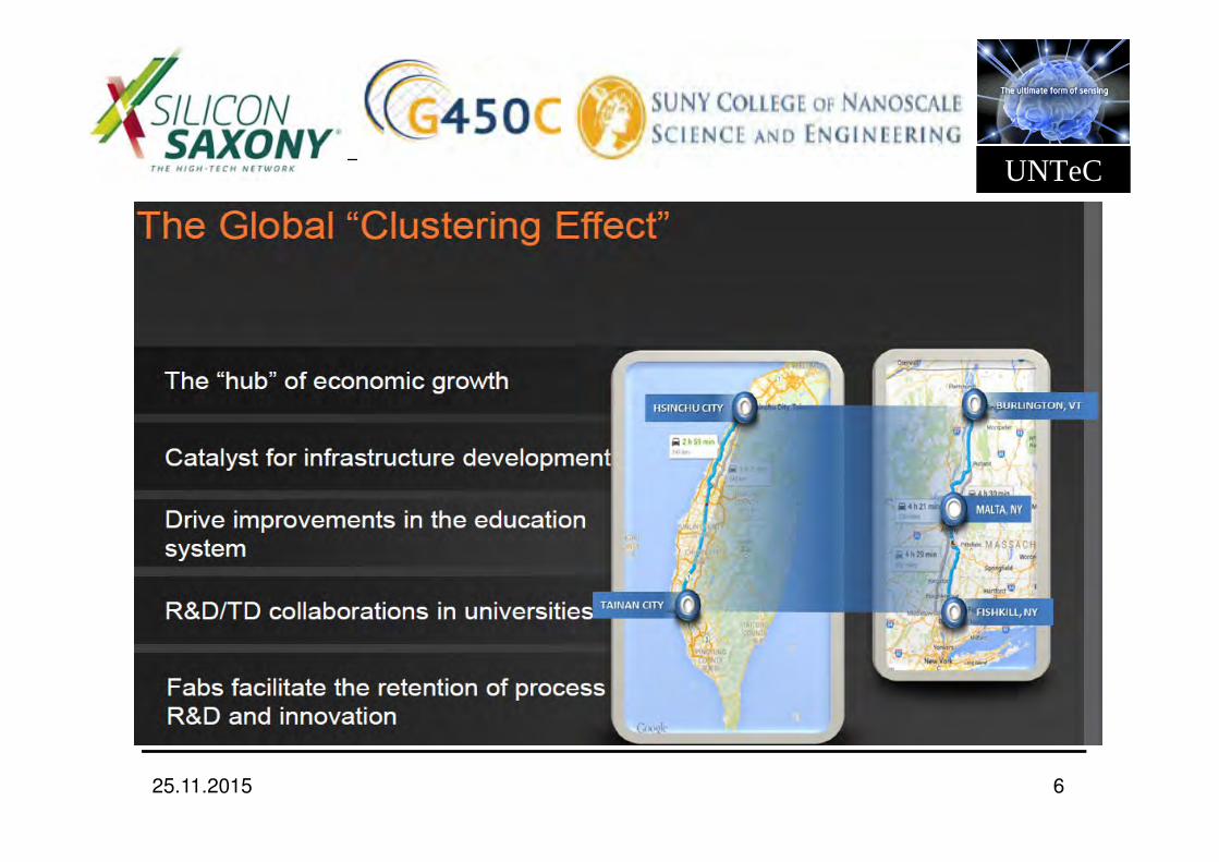
� Transforms Upstate NY into GF’s most important location
UNTeC
25.11.2015 4
UNTeC
25.11.2015 5
UNTeC
25.11.2015 6
UNTeC
25.11.2015 7
UNTeC
25.11.2015 8
UNTeC
Outlook
�Generelle Entwicklungen in Albany – GF Status Quo
�Neueste CNSE Kooperationen
�New York Power Electronics Manufacturing
Consortium - SiC Prozesslinie am CNSEConsortium - SiC Prozesslinie am CNSE
�Nano Utica News
� 450mm /EUV Quo Vadis
�Photonics/Advanced Packaging
�Summary
25.11.2015 9
UNTeC
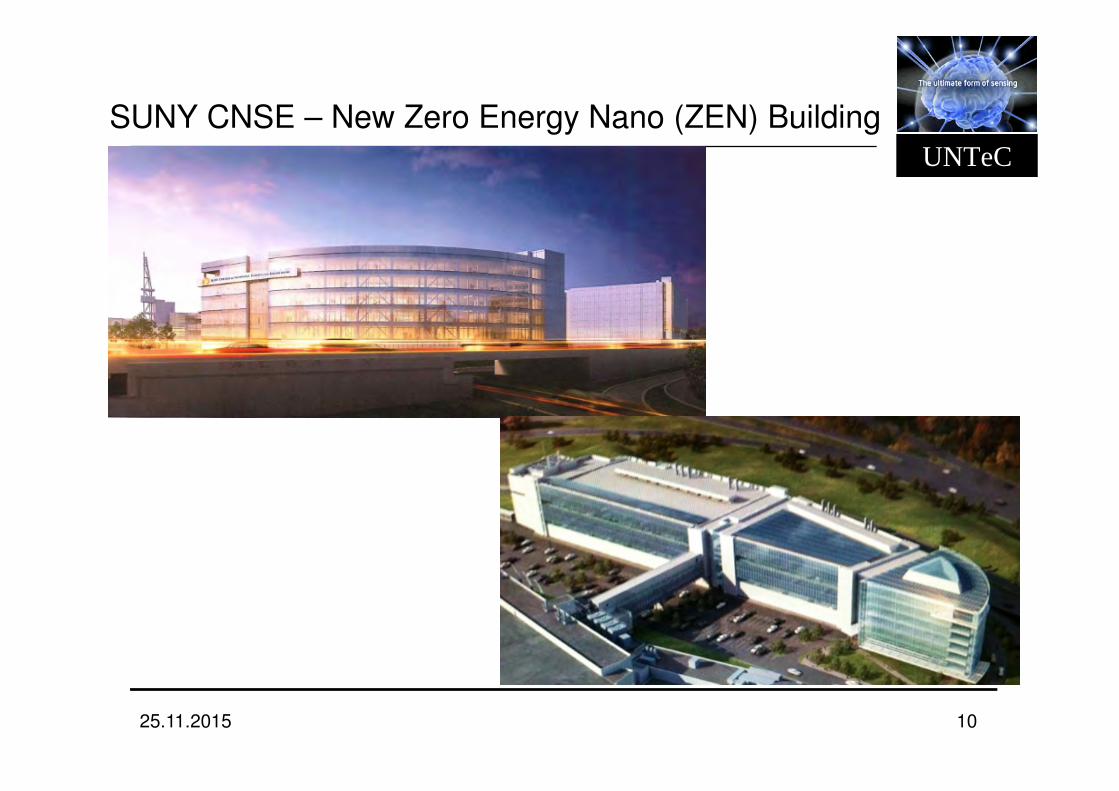
SUNY CNSE – New Zero Energy Nano (ZEN) Building
25.11.2015 10
UNTeC
Zero Energy Nano Building - ZEN
• CNSE newest building opened - ZEN is a mixed-use, clean energy facility. It will house businesses, meeting centers, and learning space and even generate its own power. 6 floor building with nearly 400,000 sq foot
• It stands prominently overlooking Interstate 90 in Albany and is housing –M&W HQ, State IT center, Commerce Hub, DPS,….
• NEDO / SUNY CNSE collaboration - $25M Partnership to Develop State-of-the-Art Technologies at CNSE’s Zero Energy Nano Building, One of theWorld’s Largest Mixed-Use, Net-Zero Energy BuildingsWorld’s Largest Mixed-Use, Net-Zero Energy Buildings
• NEDO (New Energy and Industrial Technology Development Organization), isa public scientific and technological R&D organization that promotes researchand development as well as the dissemination of industrial, energy, andenvironmental technologies in Japan. NEDO addresses energy and globalenvironmental problems and enhance industrial technology, and theorganization will cooperate to implement the ZEN project with ShimizuCorporation and deploy their new technologies such as Smart BEMS, daylightand human factors control for lighting and HVAC, and fuel cells, among others.www.nedo.go.jp/english/.
25.11.2015 11
UNTeC
New CNSE Albany collaborations…
• SEMATECH is merging with the SUNY Polytechnic
Institute
• SUNY Poly and Sematech Announce Air Products Joins Cutting-Edge CMP Center At Albany
• Mitsubishi Chemical joining nanotech research • Mitsubishi Chemical joining nanotech research
center
• $1.5 Million Investment Over First 3 Years Will Support up to 30 Jobs as Hitachi Chemical Establishes First Facility Outside of Japan for R&D of Advanced Slurry Technology
25.11.2015 12
UNTeC
Outlook
�Generelle Entwicklungen in Albany – GF Status Quo
�Neueste CNSE Kooperationen
�New York Power Electronics Manufacturing
Consortium - SiC Prozesslinie am CNSEConsortium - SiC Prozesslinie am CNSE
�Nano Utica News
� 450mm /EUV Quo Vadis
�Photonics/Advanced Packaging
�Summary
25.11.2015 13
UNTeC
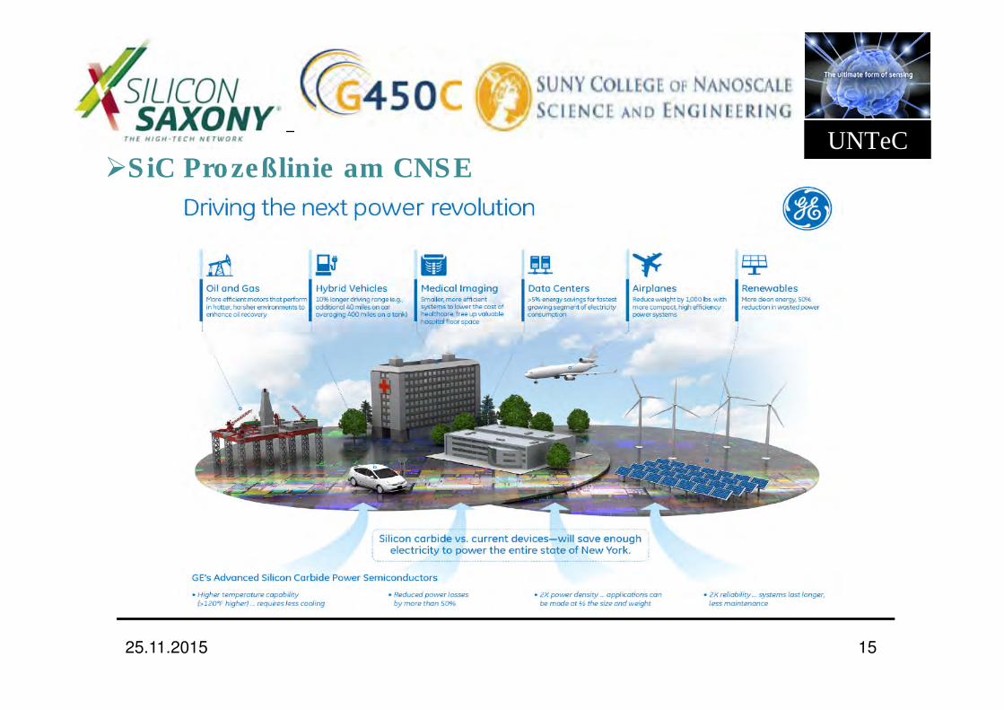
• Projekt läuft gemäß Zeitplan, Fab Retrofit in Albany im Gange• Location ist das CNSE in Albany (eine der alten RR Flächen wird umgebaut)• Leitpartner ist GE der auch die Technologie bereitstellt, Betrieb der Linie erfolgt durch CNSE – „not only development but real small volume manufacturing!“•6“ facility mit 200mm Fähigkeit wo möglich / angebracht (kein stringentes MUSS!)
�New York Power Electronics Manufacturing Consortium�SiC Prozeßlinie am CNSE
25.11.2015 14
•6“ facility mit 200mm Fähigkeit wo möglich / angebracht (kein stringentes MUSS!)• Linie wird klassisch manuell betrieben werden, keine Automatisierung!• Designpunkt -> 15k wfr/year zum Start (40k wfr/year in 2017/18), • Q1/2016 erste Starts, Qual in Mid‘16 – proven technology von GE• Gerätebestellungen erfolgt• „two of a kind tool Forderung“ keine bindende Notwendigkeit, zumindest zum Start• Applikationsfokus – Energie /Smart City! Automotive spielt im Nahzeitraum (3Jahre) noch keine Rolle• Managementverantwortung CNSE liegt bei Paul Farrar• …aber GE Research mehr und mehr in der Treiberrolle
UNTeC
�SiC Prozeßlinie am CNSE
25.11.2015 15
UNTeC
Outlook
�Generelle Entwicklungen in Albany – GF Status Quo
�Neueste CNSE Kooperationen
�New York Power Electronics Manufacturing
Consortium - SiC Prozesslinie am CNSEConsortium - SiC Prozesslinie am CNSE
�Nano Utica News
� 450mm /EUV Quo Vadis
�Photonics/Advanced Packaging
�Summary
25.11.2015 16
UNTeC
25.11.2015 17
UNTeC
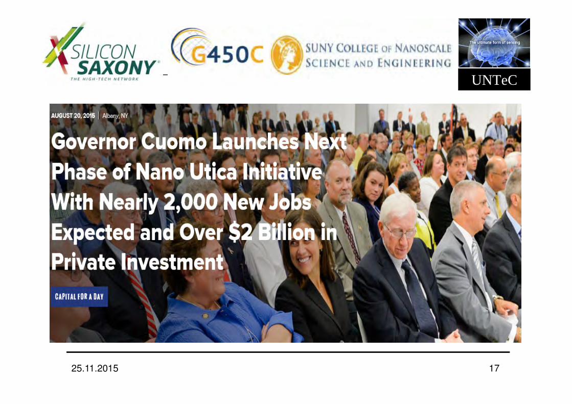
ams – a Global Leader in Advanced Sensor Technologies and analog IC’s – to generate more than 1,000 new jobs and initially invest $2 billion to support new 360,000 square foot state-of-the-art manufacturing facility at the Nano Utica site in Marcy. Construction of the ams fab is scheduled to begin in spring 2016 at the 450-acre Marcy Nanocenter site. Capital purchases, operating expenses and other investments in the facility over the first 20 years are estimated at more than $2
ams – New Waferfab at Nano Utica Site
25.11.2015 18
investments in the facility over the first 20 years are estimated at more than $2 billion
ams Chief Operating Officer Dr. Thomas Stockmeier said, “Building a new wafer fab will help us achieve our growth plans and meet the increasing demand for our advanced manufacturing nodes. Our decision to locate the facility in New York was motivated by the highly-skilled workforce, the proximity to esteemed education and research institutions, and the favorable business environment provided by Governor Cuomo and all the public and private partners we are working with on this important project.”
UNTeC
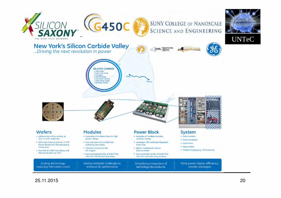
GE Global Research will expand its New York global operations to the MohawkValley, serving as the anchor tenant of the Computer Chip Commercialization Center(QUAD C) on the campus of SUNY Polytechnic Institute in Utica. Nearly 500 jobsare expected to be created in the Mohawk Valley in the next five years from SUNYPoly, GE and affiliated corporations and another 350 in the subsequent five years
GE Power Electronics Packaging Facility
25.11.2015 19
Advanced packaging technologies are vital in the development of faster and morepowerful computer chips, as well as silicon carbide chips for power electronicsapplications. The packaging facility at QUAD C will lead to commercialbreakthroughs in an array of applications ranging from defense, super-computing,tablets, cell phones, and a myriad of power electronics applications.The packaging facility is a critical component of the New York Power ElectronicsManufacturing Consortium, the governor’s $500 million public-private semiconductorresearch partnership that includes over 100 companies. Based at the SUNY PolyMegaplex in Albany with lead partners including GE and IBM, the Consortium isdriving coordinated materials research and job creation across the Upstate corridor.
UNTeC
25.11.2015 20
UNTeC
Outlook
�Generelle Entwicklungen in Albany – GF Status Quo
�Neueste CNSE Kooperationen
�New York Power Electronics Manufacturing
Consortium - SiC Prozesslinie am CNSEConsortium - SiC Prozesslinie am CNSE
�Nano Utica News
� 450mm /EUV Quo Vadis
�Photonics/Advanced Packaging
�Summary
25.11.2015 21
UNTeC
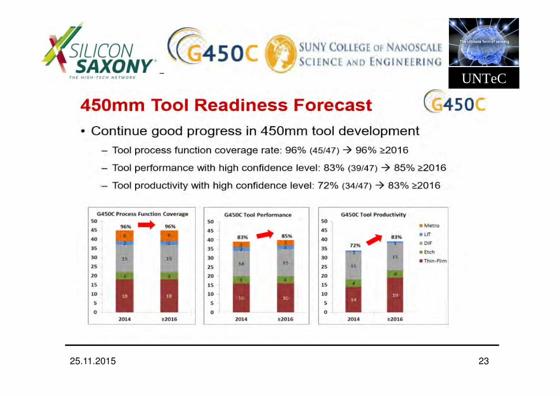
• G450C bringt weiter Tools ein (50 on site), Finanzierung durch member companieson extended schedule zunächst bis E2017 abgesichert – 2020+ Zeitleiste für HVM im formalen wording akzeptiert• Nikon 450 Scanner bei G450C Albany wie geplant installiert
• Erste wafer auf dem gesamten Litho Cluster prozessiert
�450mm / EUV Quo Vadis
25.11.2015 22
UNTeC
25.11.2015 23
UNTeC
25.11.2015 24
UNTeC
Outlook
�Generelle Entwicklungen in Albany – GF Status Quo
�Neueste CNSE Kooperationen
�New York Power Electronics Manufacturing
Consortium - SiC Prozesslinie am CNSEConsortium - SiC Prozesslinie am CNSE
�Nano Utica News
� 450mm /EUV Quo Vadis
�Photonics
�Summary
25.11.2015 25
UNTeC
•Photonics Wie im Frühjahr diskutiert, hatte sich SUNY CNSE gemeinsam mitRochester und einer Reihe von schwergewichtigen Industriepartnern für dasnational ausgeschriebene Photonics Technologieentwicklungs- / Fertigungszentrumbeworben. Status während unseres letzten Reviews war, dass die Bewerbung dienächste Hürde erfolgreich übersprungen hatte, sprich es der Antrag unter die letztendrei Bewerber geschafft hatte – verbliebene Mitkonkurrenten waren noch Florida
Integrated Photonics Institute
25.11.2015 26
und Calif/LA.
Unter Führung von Michael Liehr wurde dann mit den Partnern das verfeinerteKonzept erarbeitet und das Proposal für die finale Evaluierung zusammengestellt.Die Entscheidung, wer letztendlich den Zuschlag erhält sollte Mai/Juni erfolgen. D.h.sollte NY mit seiner Bewerbung erfolgreich sein würden in 2H 2015 die Planungenfür das Zentrum erfolgen, Start der Baumaßnahmen anlaufen und dann in 2016 diegerätetechnischen Anschaffungen anstehen.
UNTeC
•Photonics Wie früher bereits angedeutet, hat sich SUNY CNSE gemeinsam mit Rochester und einer Reihe von schwergewichtigen Industriepartnern für das national ausgeschriebene Photonics Technologieentwicklungs- / Fertigungszentrum beworben. Status ist, dass die Bewerbung nun die nächste Hürde erfolgreich übersprungen hat, sprich es der Antrag unter die letzten drei Bewerber geschafft hat
�
25.11.2015 27
– verbliebene Mitkonkurrenten sind nun offensichtlich noch Florida und Calif/LA. Unter Führung von Michael Liehr wird aktuell gemeinsam mit den Partnern das verfeinerte Konzept erarbeitet und das Proposal für die finale Evaluierung zusammengestellt. Die Entscheidung, wer letztendlich den Zuschlag erhält soll Mai/Juni erfolgen. D.h. sollte NY mit seiner Bewerbung erfolgreich sein würden in 2H 2015 die Planungen für das Zentrum erfolgen, Start der Baumaßnahmen anlaufen und dann in 2016 die gerätetechnischen Anschaffungen anstehen.
UNTeC
New York has been selected by the Department of Defense to lead a prestigious,multi-state Integrated Photonics Institute for Manufacturing Innovation. Theselection is part of a White House initiative to secure the United States’ globalleadership in emerging technology research, development, and manufacturing.Photonics harnesses the power of light to move data at great speeds, and theresearch done at the new Institute will integrate photonics components to
Integrated Photonics Institute
25.11.2015 28
research done at the new Institute will integrate photonics components torevolutionize computer chips with a wide range of applications, including medicaltechnology, defense, telecommunications, the Internet, and information technology
A $110 million federal grant awarded to the SUNY Polytechnic-led “AmericanInstitute for Manufacturing Integrated Photonics” will support a high-techconsortium with business operations, a company incubator and accelerator,workforce training, and board of directors headquartered in Rochester. Totalpublic and private investment in the Photonic Institute will exceed $600 million,including more than $250 million by New York State to equip, install, and makeoperational a state-of-the-art photonics prototyping operation
UNTeC
Outlook
�Generelle Entwicklungen in Albany – GF Status Quo
�Neueste CNSE Kooperationen
�New York Power Electronics Manufacturing
Consortium - SiC Prozesslinie am CNSEConsortium - SiC Prozesslinie am CNSE
�Nano Utica News
� 450mm /EUV Quo Vadis
�Photonics/Advanced Packaging
�Summary / Conclusions
25.11.2015 29
UNTeC
Summary & Conclusions
� Staat NY hat sich mittels langfristig angelegter High-Tech Strategie, konzen-trierter Fördermaßnahmen und Nutzung enormer Hebelung über PPP-Modell (Viele Projekte mit Volumen > $300Mio) zum globalen Technologieführer entwickelt
� Fortschritte sowohl an der Leading Edge als auch auf breiter MTM Front -> Diversifizierung in Technologien plus nun auch vermehrt auf Gesamtsystemebene
� „NY NanoTech Model: Building the Innovation Economy“ steht im Zentrum Strategie ist langfristig angelegt und auch viele Rückschläge wurden hingenom-men ohne diese anzuzweifeln :
� Con‘s: IBM , GF Probleme, Sematech (Intc, Samsung), ST and Leti, ANSI, 450mm
� Pro‘s: ams Fab, GE Power, Photonics Center, SolarCity Fertigung, GE Batterieferti-gung, GF /IBM merger
� SUNY CNSE ist der landesweite, zentrale Steuerhebel – gemäß industrieller Strukturen gesteuert und geführt
� Fördergelder fliessen primär in Infrastruktur, nicht direkt an Firmen
� NY State Strategie passt hervorragend in die wieder erwachte US Philosophie –SW- und Dienstleistung sind wichtig aber ebenso HW und Industrie / Fertigung