SMSC USB2660/USB2660i DATASHEET Revision 1.1 (11-05-10) PRODUCT FEATURES Datasheet USB2660/USB2660i Ultra Fast USB 2.0 Hub and Multi-Format Flash Media Controller with Dual SD Interfaces General Description The SMSC USB2660/USB2660i is a USB 2.0 compliant, Hi- Speed hub, card reader, and protocol converter combo solution. This fully integrated single chip solution provides USB expansion and flash card media reader/writer integration. SDIO bridging is possible with custom firmware. The SMSC USB2660/USB2660i provides an ultra fast interface between a USB host and today’s popular flash media formats. The controller allows read/write capability to flash media from the following families: – Secure Digital TM (SD) – MultiMediaCard TM (MMC) – Memory Stick ® (MS) – xD-Picture Card TM (xD) 1 The USB2660/USB2660i offers a versatile, cost-effective, and energy-efficient hub controller with 2 downstream USB 2.0 ports. This combo solution leverages SMSC’s innovative technology that delivers industry-leading data throughput in mixed-speed USB environments. Average sustained transfer rates exceeding 35 MB/s are possible 2 . Highlights 2 exposed Hi-Speed USB 2.0 downstream ports for external peripheral expansion The dedicated flash media reader is internally attached to a 3rd downstream port of the hub as a USB Compound Device — a single or multiplexed flash media reader interface — a non-multiplexed SD/SDIO interface (slot) for SD card reader or SDIO bridging applications PortMap — Flexible port mapping and port disable sequencing supports multiple platform designs PortSwap — Programmable USB differential-pair pin locations eases PCB design by aligning USB signal traces directly to connectors PHYBoost — Programmable USB transceiver drive strength recovers signal integrity 1.For xD-Picture Card TM support, please obtain a user license from the xD-Picture Card License Office. 2.Host and media dependent. Features Compliance with the following flash media card specifications SD 2.0 / MMC 4.2 / MS 1.43 / MS-Pro 1.02 / MS-Pro-HG 1.01 / MS-Duo 1.10 / xD 1.2 Supports a single external 3.3 V supply source; internal regulators provide 1.8 V internal core voltage for additional bill of materials and power savings The transaction translator (TT) in the hub supports operation of Full-Speed and Low-Speed peripherals 9 K RAM | 64 K on-chip ROM Enhanced EMI rejection and ESD protection performance Hub and flash media reader/writer configuration from a single source: External I 2 C ® ROM or external SPI ROM — Configures internal code using an external I 2 C EEPROM — Supports external code using an SPI Flash EEPROM — Customizable vendor ID, product ID, and language ID if using an external EEPROM Additional SD/SDIO port for card reader or to host wireless applications such as WiFi TM , Bluetooth ® , and GPS Up to 20 configurable GPIOs for special functions The USB2660 supports the commercial temperature range of 0°C to +70°C The USB2660i supports the industrial temperature range of -40°C to +85°C 64-pin QFN lead-free, RoHS compliant package (9 x 9 mm) Applications Desktop and mobile PCs Printers GPS navigation systems Media players/viewers Consumer A/V Set-top boxes Industrial products
Ultra Fast USB 2.0 Hub and Multi-Format Flash Media Controller with Dual SD Interfaces
General Description
The SMSC USB2660/USB2660i is a USB 2.0 compliant, Hi-Speed hub, card reader, and protocol converter combosolution. This fully integrated single chip solution provides USBexpansion and flash card media reader/writer integration. SDIObridging is possible with custom firmware. The SMSCUSB2660/USB2660i provides an ultra fast interface between aUSB host and today’s popular flash media formats. Thecontroller allows read/write capability to flash media from thefollowing families:
The USB2660/USB2660i offers a versatile, cost-effective, andenergy-efficient hub controller with 2 downstream USB 2.0ports. This combo solution leverages SMSC’s innovativetechnology that delivers industry-leading data throughput inmixed-speed USB environments. Average sustained transferrates exceeding 35 MB/s are possible2.
Highlights
2 exposed Hi-Speed USB 2.0 downstream ports for external peripheral expansionThe dedicated flash media reader is internally attached to a 3rd downstream port of the hub as a USB Compound Device — a single or multiplexed flash media reader interface— a non-multiplexed SD/SDIO interface (slot) for SD card reader
or SDIO bridging applicationsPortMap— Flexible port mapping and port disable sequencing supports
multiple platform designsPortSwap— Programmable USB differential-pair pin locations eases PCB
design by aligning USB signal traces directly to connectorsPHYBoost— Programmable USB transceiver drive strength recovers signal
integrity
1.For xD-Picture CardTM support, please obtain a user licensefrom the xD-Picture Card License Office. 2.Host and media dependent.
Features
Compliance with the following flash media card specifications SD 2.0 / MMC 4.2 / MS 1.43 / MS-Pro 1.02 / MS-Pro-HG 1.01 / MS-Duo 1.10 / xD 1.2
Supports a single external 3.3 V supply source; internal regulators provide 1.8 V internal core voltage for additional bill of materials and power savings
The transaction translator (TT) in the hub supports operation of Full-Speed and Low-Speed peripherals
9 K RAM | 64 K on-chip ROM
Enhanced EMI rejection and ESD protection performance
Hub and flash media reader/writer configuration from a single source: External I2C® ROM or external SPI ROM
— Configures internal code using an external I2C EEPROM
— Supports external code using an SPI Flash EEPROM
— Customizable vendor ID, product ID, and language ID if using an external EEPROM
Additional SD/SDIO port for card reader or to host wireless applications such as WiFiTM, Bluetooth®, and GPS
Up to 20 configurable GPIOs for special functions
The USB2660 supports the commercial temperature range of 0°C to +70°C
The USB2660i supports the industrial temperature range of -40°C to +85°C
64-pin QFN lead-free, RoHS compliant package (9 x 9 mm)
Applications
Desktop and mobile PCs
Printers
GPS navigation systems
Media players/viewers
Consumer A/V
Set-top boxes
Industrial products
ORDER NUMBERS:
USB2660/USB2660i-JZX for 64-PIN, QFN LEAD-FREE RoHS COMPLIANT PACKAGE
THIS PRODUCT MEETS THE HALOGEN MAXIMUM CONCENTRATION VALUES PER IEC61249-2-21.
FOR ROHS COMPLIANCE AND ENVIRONMENTAL INFORMATION, PLEASE VISIT WWW.SMSC.COM/ROHS.
Circuit diagrams and other information relating to SMSC products are included as a means of illustrating typical applications. Consequently, complete information sufficient forconstruction purposes is not necessarily given. Although the information has been checked and is believed to be accurate, no responsibility is assumed for inaccuracies. SMSCreserves the right to make changes to specifications and product descriptions at any time without notice. Contact your local SMSC sales office to obtain the latest specificationsbefore placing your product order. The provision of this information does not convey to the purchaser of the described semiconductor devices any licenses under any patentrights or other intellectual property rights of SMSC or others. All sales are expressly conditional on your agreement to the terms and conditions of the most recently datedversion of SMSC's standard Terms of Sale Agreement dated before the date of your order (the "Terms of Sale Agreement"). The product may contain design defects or errorsknown as anomalies which may cause the product's functions to deviate from published specifications. Anomaly sheets are available upon request. SMSC products are notdesigned, intended, authorized or warranted for use in any life support or other application where product failure could cause or contribute to personal injury or severe propertydamage. Any and all such uses without prior written approval of an Officer of SMSC and further testing and/or modification will be fully at the risk of the customer. Copies ofthis document or other SMSC literature, as well as the Terms of Sale Agreement, may be obtained by visiting SMSC’s website at http://www.smsc.com. SMSC is a registeredtrademark of Standard Microsystems Corporation (“SMSC”). Product names and company names are the trademarks of their respective holders.
SMSC makes the following part-numbered device available for purchase only by customers who are xD-Picture Card licensees: USB2660/USB2660i.
By purchasing or ordering any of such devices, Buyer represents, warrants, and agrees that Buyer is a duly licensed Licensee under an xD-Picture CardTM License Agreementwith Fuji Photo Film Co., Ltd., Olympus Optical Co., Ltd., and Toshiba Corporation; and that Buyer will maintain in effect such xD-Picture Card license and will give SMSCreasonable advance notice of any termination or expiration of such xD-Picture Card license, but in no event less than five days advance notice. SMSC may discontinue makingsuch devices available for purchase by Buyer and/or discontinue further deliveries of such devices if such xD-Picture Card license shall expire, terminate, or cease to be inforce, or if Buyer is or becomes in default of such xD-Picture Card license.
SMSC DISCLAIMS AND EXCLUDES ANY AND ALL WARRANTIES, INCLUDING WITHOUT LIMITATION ANY AND ALL IMPLIED WARRANTIES OF MERCHANTABILITY,FITNESS FOR A PARTICULAR PURPOSE, TITLE, AND AGAINST INFRINGEMENT AND THE LIKE, AND ANY AND ALL WARRANTIES ARISING FROM ANY COURSEOF DEALING OR USAGE OF TRADE. IN NO EVENT SHALL SMSC BE LIABLE FOR ANY DIRECT, INCIDENTAL, INDIRECT, SPECIAL, PUNITIVE, OR CONSEQUENTIALDAMAGES; OR FOR LOST DATA, PROFITS, SAVINGS OR REVENUES OF ANY KIND; REGARDLESS OF THE FORM OF ACTION, WHETHER BASED ON CONTRACT;TORT; NEGLIGENCE OF SMSC OR OTHERS; STRICT LIABILITY; BREACH OF WARRANTY; OR OTHERWISE; WHETHER OR NOT ANY REMEDY OF BUYER IS HELDTO HAVE FAILED OF ITS ESSENTIAL PURPOSE, AND WHETHER OR NOT SMSC HAS BEEN ADVISED OF THE POSSIBILITY OF SUCH DAMAGES.
Ultra Fast USB 2.0 Hub and Multi-Format Flash Media Controller with Dual SD Interfaces
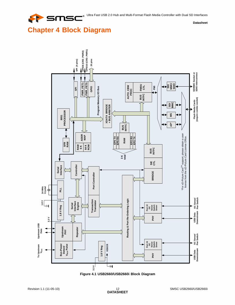
The SMSC USB2660/USB2660i is an integrated USB 2.0 compliant, Hi-Speed hub, card reader, andprotocol converter combo solution. This combo solution supports today’s popular multi-format flashmedia cards. This multi-format flash media controller and USB hub combo features two exposeddownstream USB ports available for external peripheral expansion. The dedicated flash mediareader/writer is internally attached to a third downstream port of the hub as a USB Compound Devicewhich supports the following two interfaces: One interface is multiplexed for xD-Picture Card,Memory Stick, Secure Digital/MultiMediaCard, and SD/Secure Digital Input/Output. The otherinterface is dedicated to a second SD card slot for SDIO bridging applications. SDIO bridging ispossible with custom firmware.
The USB2660/USB2660i will attach to an upstream port as a Full-Speed hub or as a Full-/Hi-Speedhub. The hub supports Low-Speed, Full-Speed, and Hi-Speed (if operating as a Hi-Speed hub)downstream devices on all of the enabled downstream ports.
All required resistors on the USB ports are integrated into the hub. This includes all seriestermination resistors on D+ and D– pins and all required pull-down and pull-up resistors. The over-current sense inputs for the downstream facing ports have internal pull-up resistors.
The USB2660/USB2660i includes programmable features such as:
PortMap which provides flexible port mapping and disable sequences. The downstream ports of aUSB2660/USB2660i hub can be reordered or disabled in any sequence to support multiple platformdesigns with minimum effort. For any port that is disabled, the USB2660/USB2660i automaticallyreorders the remaining ports to match the USB host controller’s port numbering scheme.
PortSwap which adds per-port programmability to USB differential-pair pin locations. PortSwap allows direct alignment of USB signals(D+/D-) to connectors avoiding uneven trace length or crossing ofthe USB differential signals on the PCB.
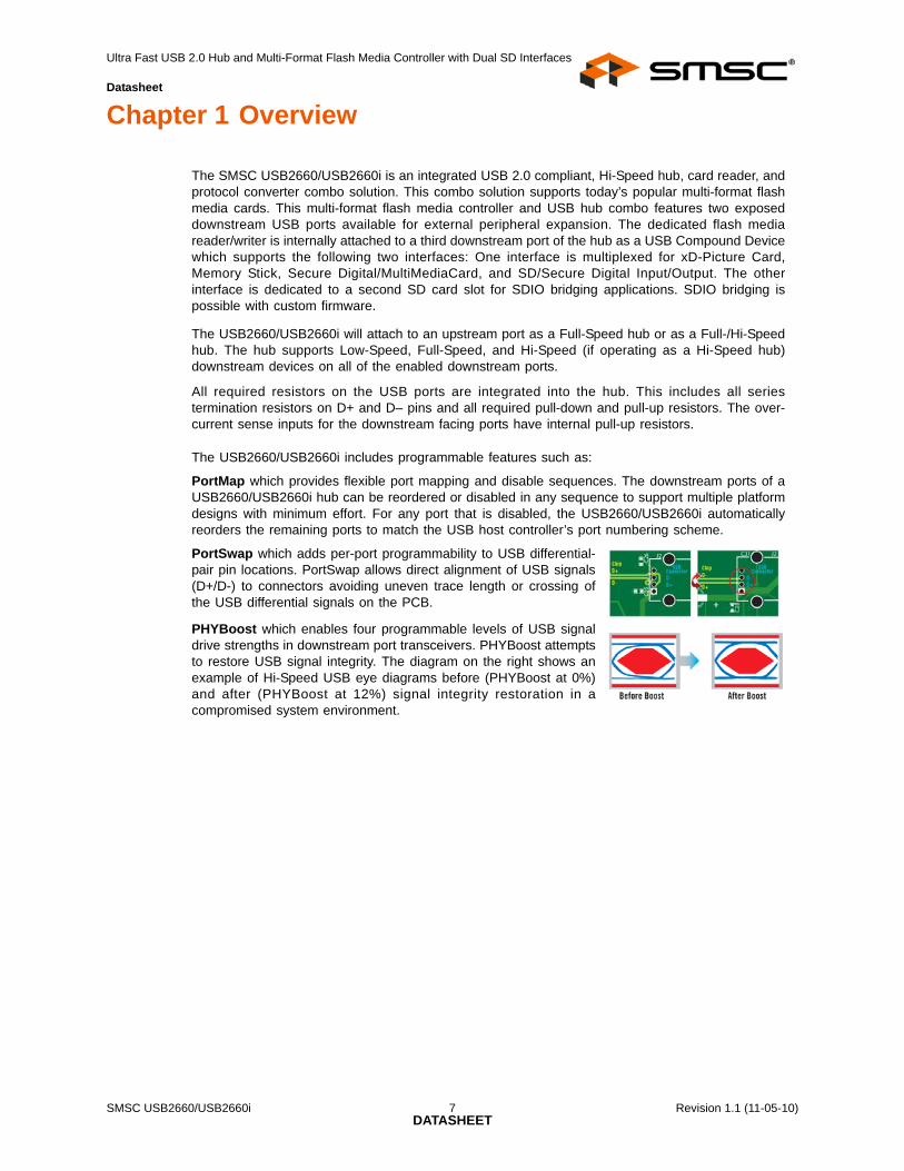
PHYBoost which enables four programmable levels of USB signaldrive strengths in downstream port transceivers. PHYBoost attemptsto restore USB signal integrity. The diagram on the right shows anexample of Hi-Speed USB eye diagrams before (PHYBoost at 0%)and after (PHYBoost at 12%) signal integrity restoration in acompromised system environment.
Ultra Fast USB 2.0 Hub and Multi-Format Flash Media Controller with Dual SD Interfaces
Hardware FeaturesSingle chip hub and flash media controller combo
USB2660 supports the commercial temperature range of 0°C to +70°C
USB2660i supports the industrial temperature range of -40°C to +85°C
Transaction translator (TT) in the hub supports operation of FS and LS peripherals
Full power management with individual or ganged power control of each downstream port
Optional support for external firmware access via SPI interface
Onboard 24 MHz crystal driver circuit
Optional external 24 MHz clock input which must be a 1.8 V signal
Code execution via SPI ROM which must meet- 30 MHz or 60 MHz operation support- Single bit or dual bit mode support- Mode 0 or mode 3 SPI support
Compliance with the following flash media card specifications:
Secure Digital 2.0 / MultiMediaCard 4.2- SD 2.0, SD-HS, SD-HC- TransFlash™ and reduced form factor media - 1/4/8 bit MMC 4.2
Memory Stick 1.43
Memory Stick Pro Format 1.02
Memory Stick Pro-HG Duo Format 1.01 - Memory Stick, MS Duo, MS-HS, MS Pro-HG, MS Pro
Memory Stick Duo 1.10
xD-Picture Card 1.2
Up to 20 GPIOs: Configuration and polarity for special function use- The number of actual GPIOs depends on the implementation configuration used- Two GPIOs available with up to 200 mA drive and protected “fold-back” short circuit current
8051 8-bit microprocessor- 60 MHz - single cycle execution- 64 KB ROM | 9 KB RAM
Integrated regulator for 1.8 V core operation
Software FeaturesHub and flash media reader/writer configuration from a single source: External I2C ROM or external SPI ROM
If the OEM is using an external EEPROM or an external SPI ROM, the following features are available:- Customizable vendor ID, product ID, and device ID- 12-hex digits maximum for the serial number string- 28-character manufacturer ID and product strings for the flash media reader/writer
Ultra Fast USB 2.0 Hub and Multi-Format Flash Media Controller with Dual SD Interfaces
OEM Selectable Hub FeaturesA default configuration is available in the USB2660/USB2660i fol lowing a reset. TheUSB2660/USB2660i may also be configured by an external I2C EEPROM or via external SPI ROMflash.
Compound Device support on a port-by-port basis - a port is permanently hardwired to a downstream USB peripheral device
Select over-current sensing and port power control on an individual or ganged (all ports together) basis to match the OEM’s choice of circuit board component selection
Port power control and over-current detection/delay features
Configure the delay time for filtering the over-current sense inputs
Configure the delay time for turning on downstream port power
Bus- or self-powered selection
Hub port disable or non-removable configurations
Flexible port mapping and disable sequencing supports multiple platform designs
Programmable USB differential-pair pin location eases PCB layout by aligning USB signal lines directly to connectors
Programmable USB signal drive strength recovers USB signal integrity using 4 levels of signal drive strength
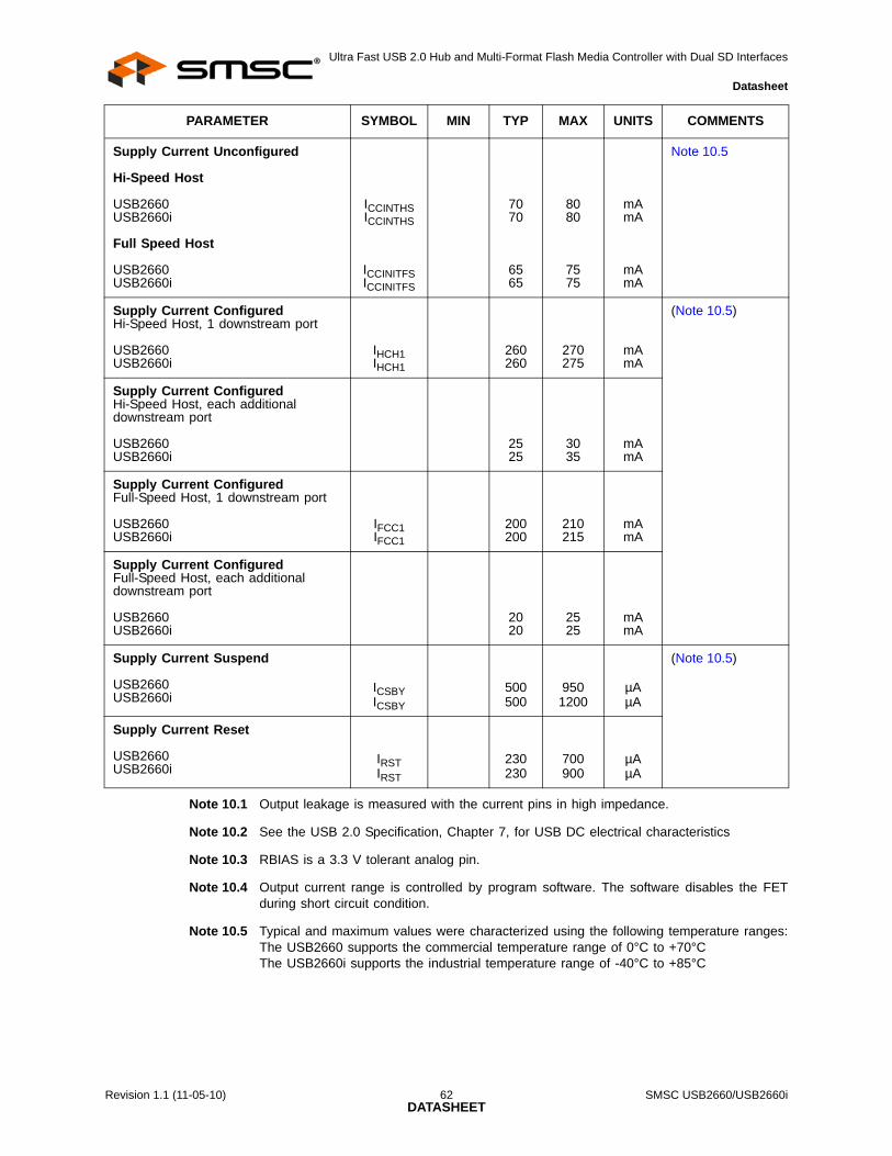
Indicate the maximum current that the 2-port hub consumes from the USB upstream port
Indicate the maximum current required for the hub controller
Ultra Fast USB 2.0 Hub and Multi-Format Flash Media Controller with Dual SD Interfaces
UINT: Unsigned Integer Standard Microsystems is a registered trademark and SMSC is a trademark of Standard Microsystems Corporation. Other product and company namesare trademarks or registered trademarks of their respective holders.
*Note: In order to develop, make, use, or sell readers and/or other products using or incorporating any of the SMSC devices made the subject of thisdocument or to use related SMSC software programs, technical information and licenses under patent and other intellectual property rights from or throughvarious persons or entities, including without limitation media standard companies, forums, and associations, and other patent holders may be required.These media standard companies, forums, and associations include without limitation the following: Sony Corporation (Memory Stick, Memory Stick Pro);SD3 LLC (Secure Digital); MultiMedia Card Association (MultiMediaCard); the SSFDC Forum (SmartMedia); the Compact Flash Association (CompactFlash); and Fuji Photo Film Co., Ltd., Olympus Optical Co., Ltd., and Toshiba Corporation (xD-Picture Card). SMSC does not make such licenses ortechnical information available; does not promise or represent that any such licenses or technical information will actually be obtainable from or throughthe various persons or entities (including the media standard companies, forums, and associations), or with respect to the terms under which they maybe made available; and is not responsible for the accuracy or sufficiency of, or otherwise with respect to, any such technical information.
SMSC's obligations (if any) under the Terms of Sale Agreement, or any other agreement with any customer, or otherwise, with respect to infringement,including without limitation any obligations to defend or settle claims, to reimburse for costs, or to pay damages, shall not apply to any of the devicesmade the subject of this document or any software programs related to any of such devices, or to any combinations involving any of them, with respectto infringement or claimed infringement of any existing or future patents related to solid state disk or other flash memory technology or applications (“SolidState Disk Patents”). By making any purchase of any of the devices made the subject of this document, the customer represents, warrants, and agreesthat it has obtained all necessary licenses under then-existing Solid State Disk Patents for the manufacture, use and sale of solid state disk and otherflash memory products and that the customer will timely obtain at no cost or expense to SMSC all necessary licenses under Solid State Disk Patents;that the manufacture and testing by or for SMSC of the units of any of the devices made the subject of this document which may be sold to the customer,and any sale by SMSC of such units to the customer, are valid exercises of the customer's rights and licenses under such Solid State Disk Patents; thatSMSC shall have no obligation for royalties or otherwise under any Solid State Disk Patents by reason of any such manufacture, use, or sale of suchunits; and that SMSC shall have no obligation for any costs or expenses related to the customer's obtaining or having obtained rights or licenses underany Solid State Disk Patents. SMSC MAKES NO WARRANTIES, EXPRESS, IMPLIED, OR STATUTORY, IN REGARD TO INFRINGEMENT OR OTHERVIOLATION OF INTELLECTUAL PROPERTY RIGHTS. SMSC DISCLAIMS AND EXCLUDES ANY AND ALL WARRANTIES AGAINSTINFRINGEMENT AND THE LIKE.
No license is granted by SMSC expressly, by implication, by estoppel or otherwise, under any patent, trademark, copyright, mask work right, trade secret,or other intellectual property right.
**To obtain this software program the appropriate SMSC Software License Agreement must be executed and in effect. Forms of these Software LicenseAgreements may be obtained by contacting SMSC.
1.I2C is a registered trademark of Philips Corporation.
Ultra Fast USB 2.0 Hub and Multi-Format Flash Media Controller with Dual SD Interfaces
This section provides a detailed description of each signal. The signals are arranged in functionalgroups according to their associated interface. The pin descriptions below are applied when using theinternal default firmware and can be referenced in Chapter 8, "Configuration Options," on page 29.Please reference Chapter 2, "Acronyms," on page 10 for a list of the acronyms used.
The “n” symbol in the signal name indicates that the active, or asserted, state occurs when the signalis at a low voltage level. When “n” is not present in the signal name, the signal is asserted at a highvoltage level.
The terms assertion and negation are used exclusively. This is done to avoid confusion when workingwith a mixture of “active low” and “active high” signals. The term assert, or assertion, indicates that asignal is active, independent of whether that level is represented by a high or low voltage. The termnegate, or negation, indicates that a signal is inactive.
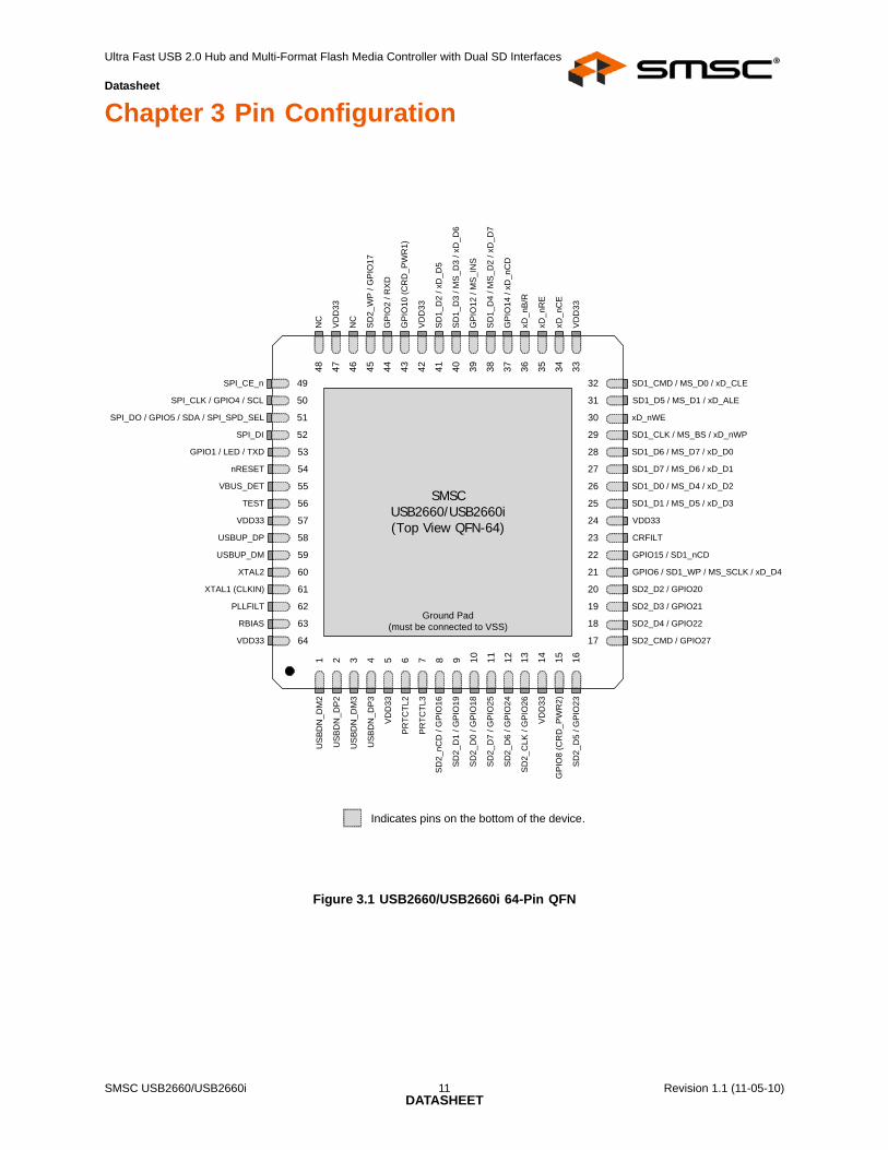
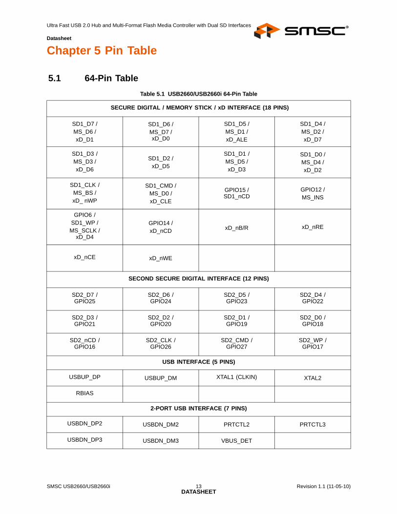
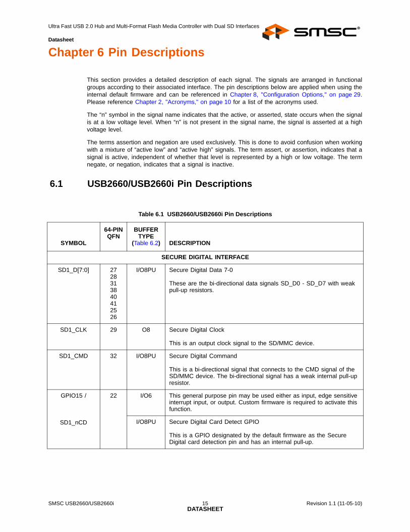
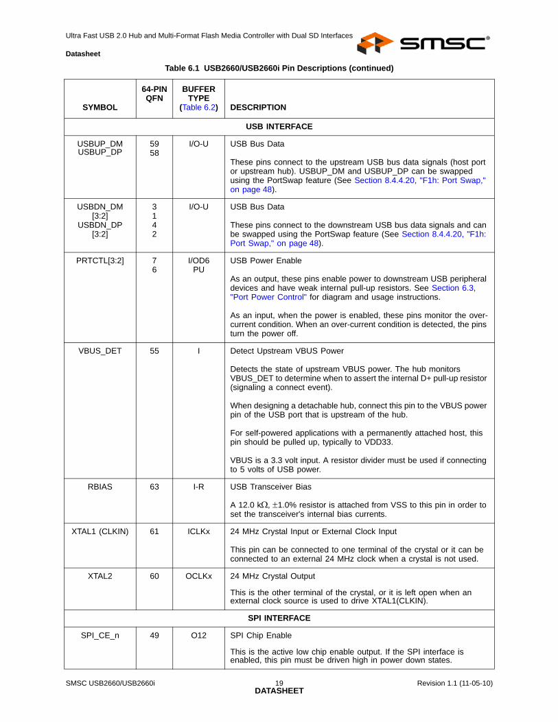
6.1 USB2660/USB2660i Pin Descriptions
Table 6.1 USB2660/USB2660i Pin Descriptions
SYMBOL
64-PIN QFN
BUFFER TYPE
(Table 6.2) DESCRIPTION
SECURE DIGITAL INTERFACE
SD1_D[7:0] 2728313840412526
I/O8PU Secure Digital Data 7-0
These are the bi-directional data signals SD_D0 - SD_D7 with weak pull-up resistors.
SD1_CLK 29 O8 Secure Digital Clock
This is an output clock signal to the SD/MMC device.
SD1_CMD 32 I/O8PU Secure Digital Command
This is a bi-directional signal that connects to the CMD signal of the SD/MMC device. The bi-directional signal has a weak internal pull-up resistor.
GPIO15 /
SD1_nCD
22 I/O6 This general purpose pin may be used either as input, edge sensitive interrupt input, or output. Custom firmware is required to activate this function.
I/O8PU Secure Digital Card Detect GPIO
This is a GPIO designated by the default firmware as the Secure Digital card detection pin and has an internal pull-up.
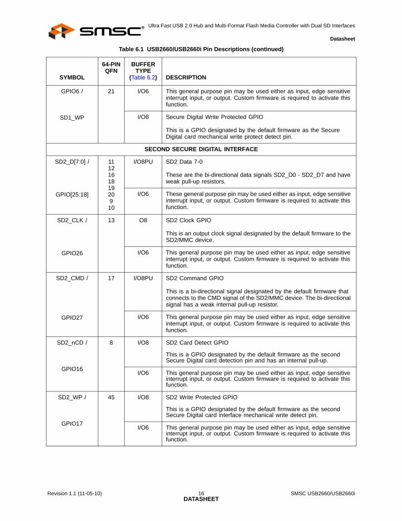
Ultra Fast USB 2.0 Hub and Multi-Format Flash Media Controller with Dual SD Interfaces
21 I/O6 This general purpose pin may be used either as input, edge sensitive interrupt input, or output. Custom firmware is required to activate this function.
I/O8 Secure Digital Write Protected GPIO
This is a GPIO designated by the default firmware as the Secure Digital card mechanical write protect detect pin.
SECOND SECURE DIGITAL INTERFACE
SD2_D[7:0] /
GPIO[25:18]
111216181920910
I/O8PU SD2 Data 7-0
These are the bi-directional data signals SD2_D0 - SD2_D7 and have weak pull-up resistors.
I/O6 These general purpose pin may be used either as input, edge sensitive interrupt input, or output. Custom firmware is required to activate this function.
SD2_CLK /
GPIO26
13 O8 SD2 Clock GPIO
This is an output clock signal designated by the default firmware to the SD2/MMC device.
I/O6 This general purpose pin may be used either as input, edge sensitive interrupt input, or output. Custom firmware is required to activate this function.
SD2_CMD /
GPIO27
17 I/O8PU SD2 Command GPIO
This is a bi-directional signal designated by the default firmware that connects to the CMD signal of the SD2/MMC device. The bi-directional signal has a weak internal pull-up resistor.
I/O6 This general purpose pin may be used either as input, edge sensitive interrupt input, or output. Custom firmware is required to activate this function.
SD2_nCD /
GPIO16
8 I/O8 SD2 Card Detect GPIO
This is a GPIO designated by the default firmware as the second Secure Digital card detection pin and has an internal pull-up.
I/O6 This general purpose pin may be used either as input, edge sensitive interrupt input, or output. Custom firmware is required to activate this function.
SD2_WP /
GPIO17
45 I/O8 SD2 Write Protected GPIO
This is a GPIO designated by the default firmware as the second Secure Digital card interface mechanical write detect pin.
I/O6 This general purpose pin may be used either as input, edge sensitive interrupt input, or output. Custom firmware is required to activate this function.
This pin is connected to the bus state pin of the MS device. It is used to control the Bus States 0, 1, 2, and 3 (BS0, BS1, and BS3) of the MS device.
GPIO12 /
MS_INS
39 I/O6 This general purpose pin may be used either as input, edge sensitive interrupt input, or output. Custom firmware is required to activate this function.
IPU Memory Stick Card Insertion GPIO
This is a GPIO designated by the default firmware as the Memory Stick card detection pin and has a weak internal pull-up resistor.
MS_SCLK 21 O8 Memory Stick System Clock
This pin is an output clock signal to the MS device.
MS_D[7:0] 2827252640383132
I/O8PD Memory Stick System Data In/Out
These pins are the bi-directional data signals for the MS device. In serial mode, the most significant bit (MSB) of each byte is transmitted first by either MSC or MS device on MS_D0.
MS_D0, MS_D2, and MS_D3 have weak pull-down resistors. MS_D1 has a pull-down resistor if in parallel mode, otherwise it is disabled. In 4- or 8-bit parallel modes, all MS_D7 - MS_D0 signals have weak pull-down resistors.
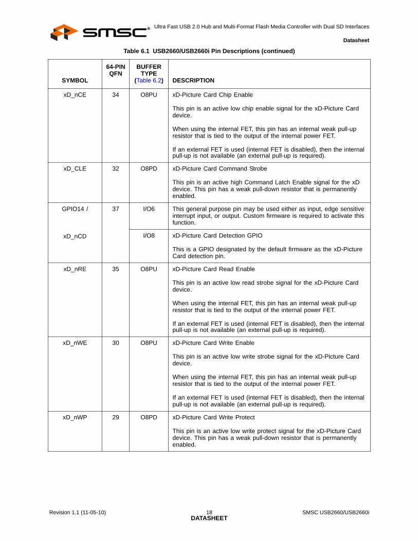
xD-PICTURE CARD INTERFACE
xD_D[7:0] 3840412125262728
I/O8PD xD-Picture Card Data 7-0
These pins are the bi-directional data signals xD_D7 - xD_D0 and have weak internal pull-down resistors.
xD_ALE 31 O8PD xD-Picture Card Address Strobe
This pin is an active high Address Latch Enable (ALE) signal for the xD device. This pin has a weak pull-down resistor that is permanently enabled.
xD_nB/R 36 IPU xD-Picture Card Busy or Data Ready
This pin is connected to the BSY/RDY pin of the xD-Picture Card device.
When using the internal FET, this pin has an internal weak pull-up resistor that is tied to the output of the internal power FET.
If an external FET is used (the internal FET is disabled), then the internal pull-up is not available (an external pull-up is required).
This pin is an active low chip enable signal for the xD-Picture Card device.
When using the internal FET, this pin has an internal weak pull-up resistor that is tied to the output of the internal power FET.
If an external FET is used (internal FET is disabled), then the internal pull-up is not available (an external pull-up is required).
xD_CLE 32 O8PD xD-Picture Card Command Strobe
This pin is an active high Command Latch Enable signal for the xD device. This pin has a weak pull-down resistor that is permanently enabled.
GPIO14 /
xD_nCD
37 I/O6 This general purpose pin may be used either as input, edge sensitive interrupt input, or output. Custom firmware is required to activate this function.
I/O8 xD-Picture Card Detection GPIO
This is a GPIO designated by the default firmware as the xD-Picture Card detection pin.
xD_nRE 35 O8PU xD-Picture Card Read Enable
This pin is an active low read strobe signal for the xD-Picture Card device.
When using the internal FET, this pin has an internal weak pull-up resistor that is tied to the output of the internal power FET.
If an external FET is used (internal FET is disabled), then the internal pull-up is not available (an external pull-up is required).
xD_nWE 30 O8PU xD-Picture Card Write Enable
This pin is an active low write strobe signal for the xD-Picture Card device.
When using the internal FET, this pin has an internal weak pull-up resistor that is tied to the output of the internal power FET.
If an external FET is used (internal FET is disabled), then the internal pull-up is not available (an external pull-up is required).
xD_nWP 29 O8PD xD-Picture Card Write Protect
This pin is an active low write protect signal for the xD-Picture Card device. This pin has a weak pull-down resistor that is permanently enabled.
These pins connect to the upstream USB bus data signals (host port or upstream hub). USBUP_DM and USBUP_DP can be swapped using the PortSwap feature (See Section 8.4.4.20, "F1h: Port Swap," on page 48).
USBDN_DM[3:2]
USBDN_DP[3:2]
3142
I/O-U USB Bus Data
These pins connect to the downstream USB bus data signals and can be swapped using the PortSwap feature (See Section 8.4.4.20, "F1h: Port Swap," on page 48).
PRTCTL[3:2] 76
I/OD6PU
USB Power Enable
As an output, these pins enable power to downstream USB peripheral devices and have weak internal pull-up resistors. See Section 6.3, "Port Power Control" for diagram and usage instructions.
As an input, when the power is enabled, these pins monitor the over-current condition. When an over-current condition is detected, the pins turn the power off.
VBUS_DET 55 I Detect Upstream VBUS Power
Detects the state of upstream VBUS power. The hub monitors VBUS_DET to determine when to assert the internal D+ pull-up resistor (signaling a connect event).
When designing a detachable hub, connect this pin to the VBUS power pin of the USB port that is upstream of the hub.
For self-powered applications with a permanently attached host, this pin should be pulled up, typically to VDD33.
VBUS is a 3.3 volt input. A resistor divider must be used if connecting to 5 volts of USB power.
RBIAS 63 I-R USB Transceiver Bias
A 12.0 kΩ, ±1.0% resistor is attached from VSS to this pin in order to set the transceiver's internal bias currents.
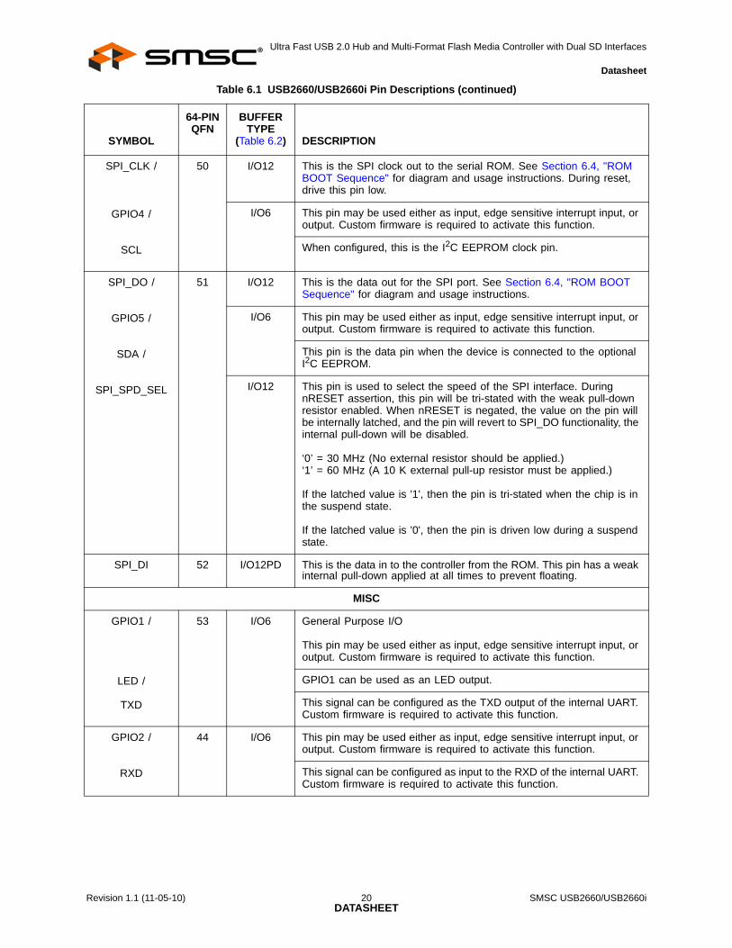
50 I/O12 This is the SPI clock out to the serial ROM. See Section 6.4, "ROM BOOT Sequence" for diagram and usage instructions. During reset, drive this pin low.
I/O6 This pin may be used either as input, edge sensitive interrupt input, or output. Custom firmware is required to activate this function.
When configured, this is the I2C EEPROM clock pin.
SPI_DO /
GPIO5 /
SDA /
SPI_SPD_SEL
51 I/O12 This is the data out for the SPI port. See Section 6.4, "ROM BOOT Sequence" for diagram and usage instructions.
I/O6 This pin may be used either as input, edge sensitive interrupt input, or output. Custom firmware is required to activate this function.
This pin is the data pin when the device is connected to the optional I2C EEPROM.
I/O12 This pin is used to select the speed of the SPI interface. During nRESET assertion, this pin will be tri-stated with the weak pull-down resistor enabled. When nRESET is negated, the value on the pin will be internally latched, and the pin will revert to SPI_DO functionality, the internal pull-down will be disabled.
‘0’ = 30 MHz (No external resistor should be applied.)‘1’ = 60 MHz (A 10 K external pull-up resistor must be applied.)
If the latched value is '1', then the pin is tri-stated when the chip is in the suspend state.
If the latched value is '0', then the pin is driven low during a suspend state.
SPI_DI 52 I/O12PD This is the data in to the controller from the ROM. This pin has a weak internal pull-down applied at all times to prevent floating.
MISC
GPIO1 /
LED /
TXD
53 I/O6 General Purpose I/O
This pin may be used either as input, edge sensitive interrupt input, or output. Custom firmware is required to activate this function.
GPIO1 can be used as an LED output.
This signal can be configured as the TXD output of the internal UART. Custom firmware is required to activate this function.
GPIO2 /
RXD
44 I/O6 This pin may be used either as input, edge sensitive interrupt input, or output. Custom firmware is required to activate this function.
This signal can be configured as input to the RXD of the internal UART. Custom firmware is required to activate this function.
15 I/O200 Card power drive: 3.3 V (100 mA or 200 mA)
This pin specifically powers the second Secure Digital interface (slot). If card power is not being used to power the second SD interface, this pin may be used as a GPIO.
Please reference Section 8.4.5.9, "147h-14Bh: Device to LUN Mapping," on page 52.
GPIO10 (CRD_PWR1)
43 I/O200 Card power drive: 3.3 V (100 mA or 200 mA)
This pin powers the multiplexed flash media interface (slot) for xD, MS, and SD/MMC. If card power is not being used to power the multiplexed flash media interface, this pin may be used as a GPIO.
Please reference Section 8.4.2.3, "A4h-A5h: Smart Media Device Power Configuration," on page 39.
nRESET 54 IS RESET Input
The system uses this active low signal reset the chip. The active low pulse should be at least 1 μs wide.
TEST 56 I TEST Input
Tie this pin to ground for normal operation.
DIGITAL / POWER / GROUND
CRFILT 23 VDD Core Regulator Filter Capacitor
This pin requires a 1.0 μF (or greater) ± 20% (ESR <0.1Ω) capacitor to VSS.
6.3 Port Power ControlPort Power control using a USB Power Switch
The USB2660/USB2660i has a single port power control and over-current sense signal for eachdownstream port. When disabling port power, the driver will actively drive a '0'. To avoid unnecessarypower dissipation, the internal pull-up resistor will be disabled at that time. When port power is enabled,the output driver is disabled, and the pull-up resistor is enabled creating an open drain output.
If there is an over-current situation, the USB Power Switch will assert the open drain OCS signal. TheSchmitt trigger input will detect this event as a low. The open drain output does not interfere. Theinternal over-current sense filter handles the transient conditions, such as low voltage, while the deviceis powering up.
Figure 6.1 Port Power Control with USB Power Switch
USB Power Switch
5 V
USB Device
PRTCTL3
EN
OCS
USB Power Switch
5 V
USB Device
PRTCTL2
EN
OCS
USB2660/60i
Ultra Fast USB 2.0 Hub and Multi-Format Flash Media Controller with Dual SD Interfaces
When using the USB2660/USB2660i with a poly fuse, an external diode must be used (SeeFigure 6.2). When disabling port power, the USB2660/USB2660i will drive a '0'. This procedure willhave no effect since the external diode will isolate the pin from the load. When port power is enabled,the USB2660/USB2660i output driver is disabled, and the pull-up resistor is enabled which creates anopen drain output. This open drain output condition means that the pull-up resistor is providing 3.3volts to the anode of the diode. If there is an over-current situation, the poly fuse will open. This willcause the cathode of the diode to go to zero volts. The anode of the diode will be at 0.7 volts, andthe Schmitt trigger input will register this as a low resulting in an over-current detection. The open drainoutput does not interfere.
Figure 6.2 Port Power Control with a Single Poly Fuse and Multiple Loads
When using a single poly fuse to power all devices, note that for the ganged situation, all power controlpins must be tied together.
Figure 6.3 Port Power with Ganged Control with Poly Fuse
USB Device
5 V
PRTCTL3
USB Device
5V
PRTCTL2
USB2660/60i
USBDevice
Poly Fuse
5 V
USBDevice
PRTCTL2
PRTCTL3
USB2660/60i
Ultra Fast USB 2.0 Hub and Multi-Format Flash Media Controller with Dual SD Interfaces
6.4 ROM BOOT SequenceAfter power-on reset, the internal firmware checks for an external SPI flash device that contains a validsignature of "2DFU" (device firmware upgrade) beginning at address 0xFFFA. If a valid signature isfound, then the external ROM is enabled and code execution begins at address 0x0000 in the externalSPI device. Otherwise, code execution continues from the internal ROM.
If there is no SPI ROM detected, the internal firmware then checks for the presence of an I2C ROM.The firmware looks for the signature ‘ATA2’ at the offset of FCh-FFh and ‘ecf1’ at the offset of 17Ch-17Fh in the I2C ROM. The firmware reads in the I2C ROM to configure the hardware and softwareinternally. Please refer to Section 8.3.2, "EEPROM Data Descriptor," on page 30 for the details of theconfiguration options.
The SPI ROM required for the USB2660/USB2660i is a recommended minimum of 1 Mbit and supporteither 30 MHz or 60 MHz. The frequency used is set using the SPI_SPD_SEL. For 30 MHz operation,this pin must be pulled to ground through a 100 kΩ resistor. For 60 MHz operation, this pin must pulledup through a 100 kΩ resistor.
The SPI_SPD_SEL pin is used to choose the speed of the SPI interface. During nRESET assertion,this pin will be tri-stated with the weak pull-down resistor enabled. When nRESET is negated, the valueon the pin will be internally latched, and the pin will revert to SPI_DO functionality. The internal pull-down will be disabled.
The firmware can determine the speed of operation on the SPI port by checking the SPI_SPEED inthe SPI_CTL register (0x2400 - RESET = 0x02). Both 1- and 2-bit SPI operation is supported. Foroptimum throughput, a 2-bit SPI ROM is recommended. Both mode 0 and mode 3 SPI ROMS are alsosupported.
Figure 6.4 SPI ROM Connection
Figure 6.5 I2C Connection
SPI ROM
SPI_CE_nSPI_CLK / GPIO4 / SCL
SPI_DI
SPI_DO / GPIO5 / SDA / SPI_SPD_SEL
CE#
CLK
SISO
USB2660/60i
I2C ROM
SCL
SDA
3. 3 V
3. 3 V
10 K
10 KUSB2660/60i
Ultra Fast USB 2.0 Hub and Multi-Format Flash Media Controller with Dual SD Interfaces
8.1 HubSMSC’s USB 2.0 hub is fully compliant to the Universal Serial Bus Specification available from theUSB Implementer’s Forum found at http://www.usb.org (Revision 2.0 April 27, 2000 and the 12/7/2000and 5/28/2002 Errata). Please reference Chapter 11 (Hub Specification) for general details regardinghub operation and functionality.
For performance reasons, the hub provides 1 transaction translator (TT) that is shared by bothdownstream ports defined as a single-TT configuration. The TT contains 4 non-periodic buffers.
8.1.1 Hub Configuration Options
The SMSC hub supports a large number of features (some are mutually exclusive), and must beconfigured in order to correctly function when attached to a USB host controller. There are two principalways to configure the hub:
via the internal default settings or
by settings stored in an external EEPROM or SPI Flash device.
8.1.1.1 Power Switching Polarity
The hub will only support active high power controllers.
8.1.2 VBus Detect
According to Section 7.2.1 of the USB 2.0 Specification, a device cannot provide power to its D+ orD- pull-up resistors unless the upstream port’s VBUS is in the asserted (powered) state. TheVBUS_DET pin on the hub monitors the state of the upstream VBUS signal and will not pull-up theD+ resistor if VBUS is not active. If VBUS goes from an active to an inactive state (not powered), thehub will remove power from the D+ pull-up resistor within 10 seconds.
8.2 Card ReaderThe SMSC USB2660/USB2660i is fully compliant with the following flash media card readerspecifications:
Secure Digital 2.0 / MultiMediaCard 4.2-SD 2.0, HS-SD, HC-SD-TransFlash™ and reduced form factor media -1/4/8 bit MMC 4.2
Memory Stick 1.43
Memory Stick Pro Format 1.02
Memory Stick Pro-HG Duo Format 1.01-Memory Stick, MS Duo, HS-MS, MS Pro-HG, MS Pro
Memory Stick Duo 1.10
xD-Picture Card 1.2
Ultra Fast USB 2.0 Hub and Multi-Format Flash Media Controller with Dual SD Interfaces
The USB2660/USB2660i can be configured via a 2-wire (I2C) EEPROM (512x8) or an external SPIflash device containing the firmware for the USB2660/USB2660i. If an external configuration devicedoes not exist the internal default values will be used. If one of the external devices is used forconfiguration, the OEM can update the values through the USB interface. The hub will then “attach”to the upstream USB host.
The USBDM tool set is available in the USB264x Hub Card reader combo software release package.To download the software package from SMSC's website, please visit:
to go to the OBJ Hub Card Reader Software Download Agreement. Review the license, and if youagree, check the "I agree" box and then select “Confirm”. You will then be able to download USB264xHub Card reader combo release package zip file containing the USBDM tool set.
Please note that the following applies to the system values and descriptions when used:
N/A = Not applicable to this part
Reserved = For internal use
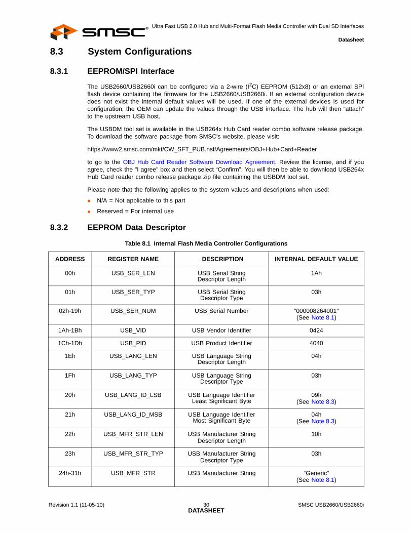
8.3.2 EEPROM Data Descriptor
Table 8.1 Internal Flash Media Controller Configurations
ADDRESS REGISTER NAME DESCRIPTION INTERNAL DEFAULT VALUE
00h USB_SER_LEN USB Serial String Descriptor Length
1Ah
01h USB_SER_TYP USB Serial String Descriptor Type
03h
02h-19h USB_SER_NUM USB Serial Number "000008264001" (See Note 8.1)
1Ah-1Bh USB_VID USB Vendor Identifier 0424
1Ch-1Dh USB_PID USB Product Identifier 4040
1Eh USB_LANG_LEN USB Language String Descriptor Length
04h
1Fh USB_LANG_TYP USB Language String Descriptor Type
03h
20h USB_LANG_ID_LSB USB Language Identifier Least Significant Byte
09h(See Note 8.3)
21h USB_LANG_ID_MSB USB Language Identifier Most Significant Byte
04h(See Note 8.3)
22h USB_MFR_STR_LEN USB Manufacturer String Descriptor Length
10h
23h USB_MFR_STR_TYP USB Manufacturer String Descriptor Type
03h
24h-31h USB_MFR_STR USB Manufacturer String “Generic”(See Note 8.1)
8.4 Set bit 7 of bmAttribute to enable the registers in Table 8.4.
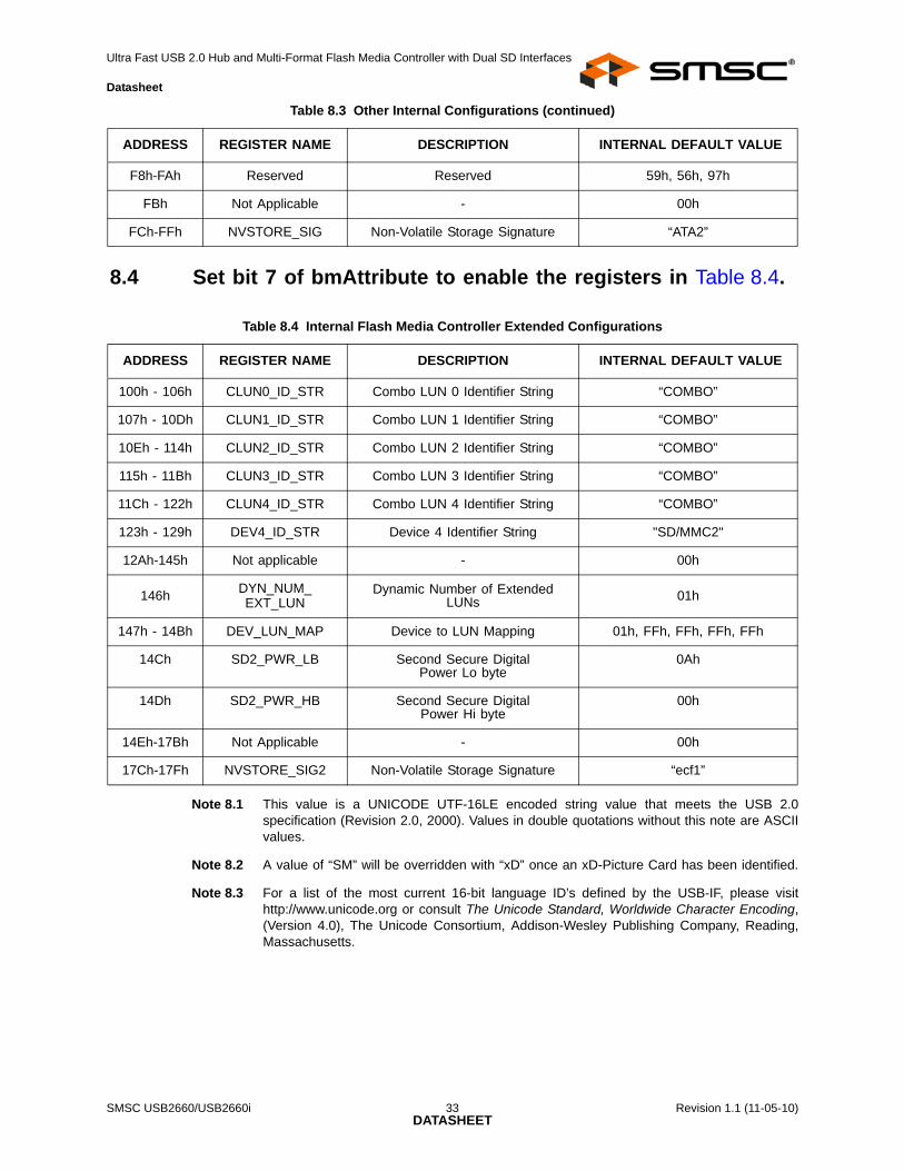
Note 8.1 This value is a UNICODE UTF-16LE encoded string value that meets the USB 2.0specification (Revision 2.0, 2000). Values in double quotations without this note are ASCIIvalues.
Note 8.2 A value of “SM” will be overridden with “xD” once an xD-Picture Card has been identified.
Note 8.3 For a list of the most current 16-bit language ID’s defined by the USB-IF, please visithttp://www.unicode.org or consult The Unicode Standard, Worldwide Character Encoding,(Version 4.0), The Unicode Consortium, Addison-Wesley Publishing Company, Reading,Massachusetts.
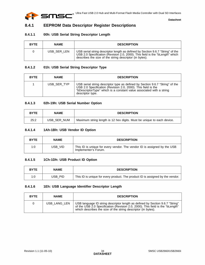
8.4.1 EEPROM Data Descriptor Register Descriptions
8.4.1.1 00h: USB Serial String Descriptor Length
8.4.1.2 01h: USB Serial String Descriptor Type
8.4.1.3 02h-19h: USB Serial Number Option
8.4.1.4 1Ah-1Bh: USB Vendor ID Option
8.4.1.5 1Ch-1Dh: USB Product ID Option
8.4.1.6 1Eh: USB Language Identifier Descriptor Length
BYTE NAME DESCRIPTION
0 USB_SER_LEN USB serial string descriptor length as defined by Section 9.6.7 “String” of the USB 2.0 Specification (Revision 2.0, 2000). This field is the “bLength” which describes the size of the string descriptor (in bytes).
BYTE NAME DESCRIPTION
1 USB_SER_TYP USB serial string descriptor type as defined by Section 9.6.7 “String” of the USB 2.0 Specification (Revision 2.0, 2000). This field is the “bDescriptorType” which is a constant value associated with a string descriptor type.
BYTE NAME DESCRIPTION
25:2 USB_SER_NUM Maximum string length is 12 hex digits. Must be unique to each device.
BYTE NAME DESCRIPTION
1:0 USB_VID This ID is unique for every vendor. The vendor ID is assigned by the USB Implementer’s Forum.
BYTE NAME DESCRIPTION
1:0 USB_PID This ID is unique for every product. The product ID is assigned by the vendor.
BYTE NAME DESCRIPTION
0 USB_LANG_LEN USB language ID string descriptor length as defined by Section 9.6.7 “String” of the USB 2.0 Specification (Revision 2.0, 2000). This field is the “bLength” which describes the size of the string descriptor (in bytes).
Ultra Fast USB 2.0 Hub and Multi-Format Flash Media Controller with Dual SD Interfaces
8.4.1.7 1Fh: USB Language Identifier Descriptor Type
8.4.1.8 20h: USB Language Identifier Least Significant Byte
8.4.1.9 21h: USB Language Identifier Most Significant Byte
8.4.1.10 22h: USB Manufacturer String Descriptor Length
8.4.1.11 23h: USB Manufacturer String Descriptor Type
8.4.1.12 24h-31h: USB Manufacturer String Option
8.4.1.13 32h-5Dh: Reserved
BYTE NAME DESCRIPTION
1 USB_LANG_TYP USB language ID string descriptor type as defined by Section 9.6.7 “String” of the USB 2.0 Specification (Revision 2.0, 2000). This field is the “bDescriptorType” which is a constant value associated with a string descriptor type.
BYTE NAME DESCRIPTION
2 USB_LANG_ID_LSB
English language code = ‘0409’. See Note 8.3 to reference additional language ID’s defined by the USB-IF.
BYTE NAME DESCRIPTION
3 USB_LANG_ID_MSB
English language code = ‘0409’. See Note 8.3 to reference additional language ID’s defined by the USB-IF.
BYTE NAME DESCRIPTION
0 USB_MFR_STR_LEN
USB manufacturer string descriptor length as defined by Section 9.6.7 “String” of the USB 2.0 Specification (Revision 2.0, 2000). This field is the “bLength” which describes the size of the string descriptor (in bytes).
BYTE NAME DESCRIPTION
1 USB_MFR_STR_TYP
USB manufacturer string descriptor type as defined by Section 9.6.7 “String” of the USB 2.0 Specification (Revision 2.0, 2000). This field is the “bDescriptorType” which is a constant value associated with a string descriptor type.
BYTE NAME DESCRIPTION
15:2 USB_MFR_STR The maximum string length is 28 characters.
BYTE NAME DESCRIPTION
59:16 Reserved Reserved.
Ultra Fast USB 2.0 Hub and Multi-Format Flash Media Controller with Dual SD Interfaces
8.4.1.14 5Eh: USB Product String Descriptor Length
8.4.1.15 5Fh: USB Product String Descriptor Type
8.4.1.16 60h-99h: USB Product String Option
8.4.1.17 9Ah: USB BmAttribute (1 byte)
8.4.1.18 9Bh: USB MaxPower (1 byte)
BYTE NAME DESCRIPTION
0 USB_PRD_STR_LEN
USB product string descriptor length as defined by Section 9.6.7 “String” of the USB 2.0 Specification (Revision 2.0, 2000). This field is the “bLength” which describes the size of the string descriptor (in bytes).
BYTE NAME DESCRIPTION
1 USB_PRD_STR_TYP
USB product string descriptor type as defined by Section 9.6.7 “String” of the USB 2.0 Specification (Revision 2.0, 2000). This field is the “bDescriptorType” which is a constant value associated with a string descriptor type.
BYTE NAME DESCRIPTION
59:2 USB_PRD_STR This string will be used during the USB enumeration process in the Windows® operating system. Maximum string length is 28 characters.
BIT NAME DESCRIPTION
7:0 USB_BM_ATT Self- or Bus-Power: Selects between self- and bus-powered operation.
The hub is either self-powered (draws less than 2 mA of upstream bus power) or bus-powered (limited to a 100 mA maximum of upstream power prior to being configured by the host controller).
When configured as a bus-powered device, the SMSC hub consumes less than 100 mA of current prior to being configured. After configuration, the bus-powered SMSC hub (along with all associated hub circuitry, any embedded devices if part of a compound device, and 100 mA per externally available downstream port) must consume no more than 500 mA of upstream VBUS current. The current consumption is system dependent, and the OEM must ensure that the USB 2.0 Specification is not violated.
When configured as a self-powered device, <1 mA of upstream VBUS current is consumed and all ports are available, with each port being capable of sourcing 500 mA of current.
80 = Bus-powered operation (default)C0 = Self-powered operationA0 = Bus-powered operation with remote wake-upE0 = Self-powered operation with remote wake-up
BIT NAME DESCRIPTION
7:0 USB_MAX_PWR USB Max Power per the USB 2.0 Specification. Do NOT set this value greater than 100 mA.
Ultra Fast USB 2.0 Hub and Multi-Format Flash Media Controller with Dual SD Interfaces
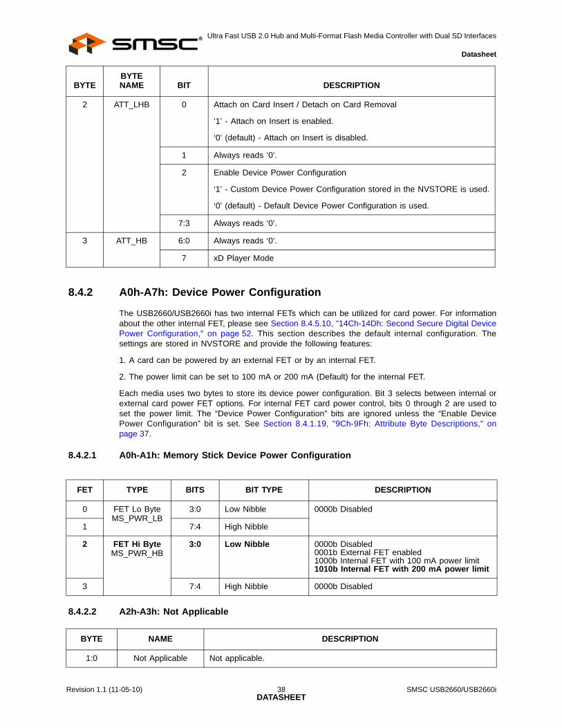
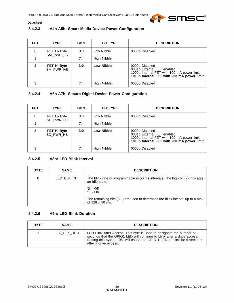
The USB2660/USB2660i has two internal FETs which can be utilized for card power. For informationabout the other internal FET, please see Section 8.4.5.10, "14Ch-14Dh: Second Secure Digital DevicePower Configuration," on page 52. This section describes the default internal configuration. Thesettings are stored in NVSTORE and provide the following features:
1. A card can be powered by an external FET or by an internal FET.
2. The power limit can be set to 100 mA or 200 mA (Default) for the internal FET.
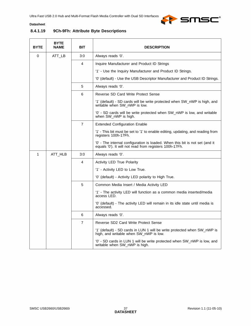
Each media uses two bytes to store its device power configuration. Bit 3 selects between internal orexternal card power FET options. For internal FET card power control, bits 0 through 2 are used toset the power limit. The “Device Power Configuration” bits are ignored unless the “Enable DevicePower Configuration” bit is set. See Section 8.4.1.19, "9Ch-9Fh: Attribute Byte Descriptions," onpage 37.
8.4.2.1 A0h-A1h: Memory Stick Device Power Configuration
8.4.2.2 A2h-A3h: Not Applicable
2 ATT_LHB 0 Attach on Card Insert / Detach on Card Removal
‘1’ - Attach on Insert is enabled.
‘0’ (default) - Attach on Insert is disabled.
1 Always reads ‘0’.
2 Enable Device Power Configuration
‘1’ - Custom Device Power Configuration stored in the NVSTORE is used.
‘0’ (default) - Default Device Power Configuration is used.
7:3 Always reads ‘0’.
3 ATT_HB 6:0 Always reads ‘0’.
7 xD Player Mode
FET TYPE BITS BIT TYPE DESCRIPTION
0 FET Lo ByteMS_PWR_LB
3:0 Low Nibble 0000b Disabled
1 7:4 High Nibble
2 FET Hi ByteMS_PWR_HB
3:0 Low Nibble 0000b Disabled0001b External FET enabled1000b Internal FET with 100 mA power limit1010b Internal FET with 200 mA power limit
3 7:4 High Nibble 0000b Disabled
BYTE NAME DESCRIPTION
1:0 Not Applicable Not applicable.
BYTEBYTE NAME BIT DESCRIPTION
Ultra Fast USB 2.0 Hub and Multi-Format Flash Media Controller with Dual SD Interfaces
8.4.2.3 A4h-A5h: Smart Media Device Power Configuration
8.4.2.4 A6h-A7h: Secure Digital Device Power Configuration
8.4.2.5 A8h: LED Blink Interval
8.4.2.6 A9h: LED Blink Duration
FET TYPE BITS BIT TYPE DESCRIPTION
0 FET Lo ByteSM_PWR_LB
3:0 Low Nibble 0000b Disabled
1 7:4 High Nibble
2 FET Hi ByteSM_PWR_HB
3:0 Low Nibble 0000b Disabled0001b External FET enabled1000b Internal FET with 100 mA power limit1010b Internal FET with 200 mA power limit
3 7:4 High Nibble 0000b Disabled
FET TYPE BITS BIT TYPE DESCRIPTION
0 FET Lo ByteSD_PWR_LB
3:0 Low Nibble 0000b Disabled
1 7:4 High Nibble
2 FET Hi ByteSD_PWR_HB
3:0 Low Nibble 0000b Disabled0001b External FET enabled1000b Internal FET with 100 mA power limit1010b Internal FET with 200 mA power limit
3 7:4 High Nibble 0000b Disabled
BYTE NAME DESCRIPTION
0 LED_BLK_INT The blink rate is programmable in 50 ms intervals. The high bit (7) indicates an idle state:
‘0’ - Off‘1’ - On
The remaining bits (6:0) are used to determine the blink interval up to a max of 128 x 50 ms.
BYTE NAME DESCRIPTION
1 LED_BLK_DUR LED Blink After Access. This byte is used to designate the number of seconds that the GPIO1 LED will continue to blink after a drive access. Setting this byte to "05" will cause the GPIO 1 LED to blink for 5 seconds after a drive access.
Ultra Fast USB 2.0 Hub and Multi-Format Flash Media Controller with Dual SD Interfaces
These bytes are used to specify the LUN descriptor returned by the device. These bytes are used incombination with the device to LUN mapping bytes in applications where the OEM wishes to reorderand rename the LUNs. If multiple devices are mapped to the same LUN (a COMBO LUN), then theCLUN#_ID_STR will be used to name the COMBO LUN instead of the individual device strings. Whenapplicable, the "SM" value will be overridden with xD once an xD-Picture Card has been identified.
8.4.3.1 AAh-B0h: Device 0 Identifier String
8.4.3.2 B1h-B7h: Device 1 Identifier String
8.4.3.3 B8h-BEh: Device 2 Identifier String
8.4.3.4 BFh-C5h: Device 3 Identifier String
8.4.3.5 C6h-CDh: Inquiry Vendor String
8.4.3.6 CEh-D2h: Inquiry Product String
BYTE NAME DESCRIPTION
6:0 DEV0_ID_STR Not applicable.
BYTE NAME DESCRIPTION
6:0 DEV1_ID_STR This ID string is associated with the Memory Stick device.
BYTE NAME DESCRIPTION
6:0 DEV2_ID_STR This ID string is associated with the Smart Media (Note 8.2) device.
BYTE NAME DESCRIPTION
6:0 DEV3_ID_STR This ID string is associated with the Secure Digital / MultiMediaCard device.
BYTE NAME DESCRIPTION
7:0 INQ_VEN_STR If bit 4 of the 1st attribute byte is set, the device will use these strings in response to a USB inquiry command, instead of the USB descriptor manufacturer and product ID strings.
BYTE NAME DESCRIPTION
4:0 INQ_PRD_STR If bit 4 of the 1st attribute byte is set, the device will use these strings in response to a USB inquiry command, instead of the USB descriptor manufacturer and product ID strings.
Ultra Fast USB 2.0 Hub and Multi-Format Flash Media Controller with Dual SD Interfaces
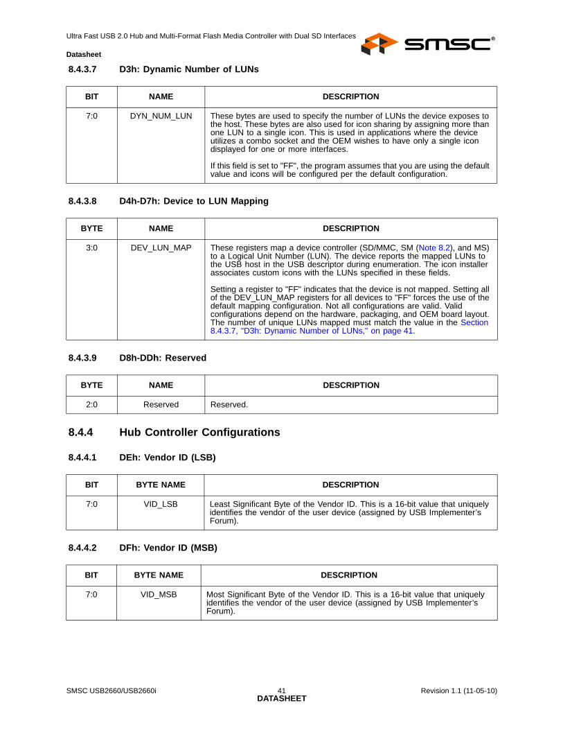
7:0 DYN_NUM_LUN These bytes are used to specify the number of LUNs the device exposes to the host. These bytes are also used for icon sharing by assigning more than one LUN to a single icon. This is used in applications where the device utilizes a combo socket and the OEM wishes to have only a single icon displayed for one or more interfaces.
If this field is set to "FF", the program assumes that you are using the default value and icons will be configured per the default configuration.
BYTE NAME DESCRIPTION
3:0 DEV_LUN_MAP These registers map a device controller (SD/MMC, SM (Note 8.2), and MS) to a Logical Unit Number (LUN). The device reports the mapped LUNs to the USB host in the USB descriptor during enumeration. The icon installer associates custom icons with the LUNs specified in these fields.
Setting a register to "FF" indicates that the device is not mapped. Setting all of the DEV_LUN_MAP registers for all devices to "FF" forces the use of the default mapping configuration. Not all configurations are valid. Valid configurations depend on the hardware, packaging, and OEM board layout. The number of unique LUNs mapped must match the value in the Section 8.4.3.7, "D3h: Dynamic Number of LUNs," on page 41.
BYTE NAME DESCRIPTION
2:0 Reserved Reserved.
BIT BYTE NAME DESCRIPTION
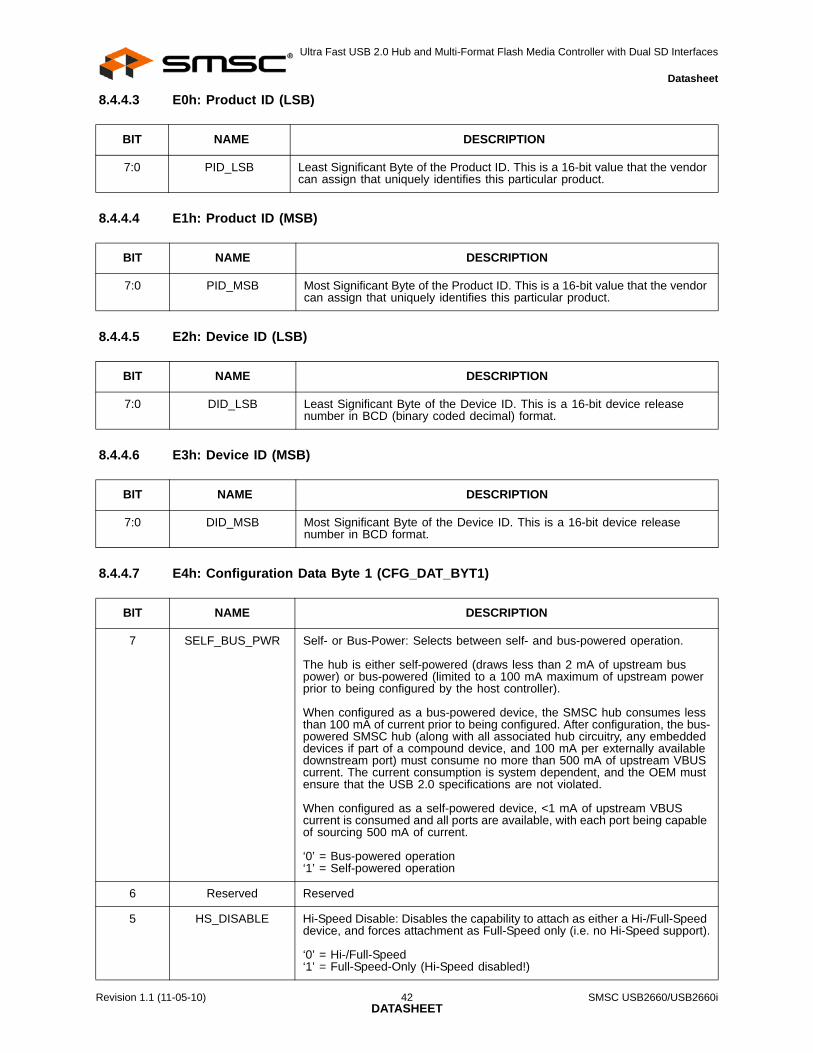
7:0 VID_LSB Least Significant Byte of the Vendor ID. This is a 16-bit value that uniquely identifies the vendor of the user device (assigned by USB Implementer’s Forum).
BIT BYTE NAME DESCRIPTION
7:0 VID_MSB Most Significant Byte of the Vendor ID. This is a 16-bit value that uniquely identifies the vendor of the user device (assigned by USB Implementer’s Forum).
Ultra Fast USB 2.0 Hub and Multi-Format Flash Media Controller with Dual SD Interfaces
8.4.4.7 E4h: Configuration Data Byte 1 (CFG_DAT_BYT1)
BIT NAME DESCRIPTION
7:0 PID_LSB Least Significant Byte of the Product ID. This is a 16-bit value that the vendor can assign that uniquely identifies this particular product.
BIT NAME DESCRIPTION
7:0 PID_MSB Most Significant Byte of the Product ID. This is a 16-bit value that the vendor can assign that uniquely identifies this particular product.
BIT NAME DESCRIPTION
7:0 DID_LSB Least Significant Byte of the Device ID. This is a 16-bit device release number in BCD (binary coded decimal) format.
BIT NAME DESCRIPTION
7:0 DID_MSB Most Significant Byte of the Device ID. This is a 16-bit device release number in BCD format.
BIT NAME DESCRIPTION
7 SELF_BUS_PWR Self- or Bus-Power: Selects between self- and bus-powered operation.
The hub is either self-powered (draws less than 2 mA of upstream bus power) or bus-powered (limited to a 100 mA maximum of upstream power prior to being configured by the host controller).
When configured as a bus-powered device, the SMSC hub consumes less than 100 mA of current prior to being configured. After configuration, the bus-powered SMSC hub (along with all associated hub circuitry, any embedded devices if part of a compound device, and 100 mA per externally available downstream port) must consume no more than 500 mA of upstream VBUS current. The current consumption is system dependent, and the OEM must ensure that the USB 2.0 specifications are not violated.
When configured as a self-powered device, <1 mA of upstream VBUS current is consumed and all ports are available, with each port being capable of sourcing 500 mA of current.
5 HS_DISABLE Hi-Speed Disable: Disables the capability to attach as either a Hi-/Full-Speed device, and forces attachment as Full-Speed only (i.e. no Hi-Speed support).
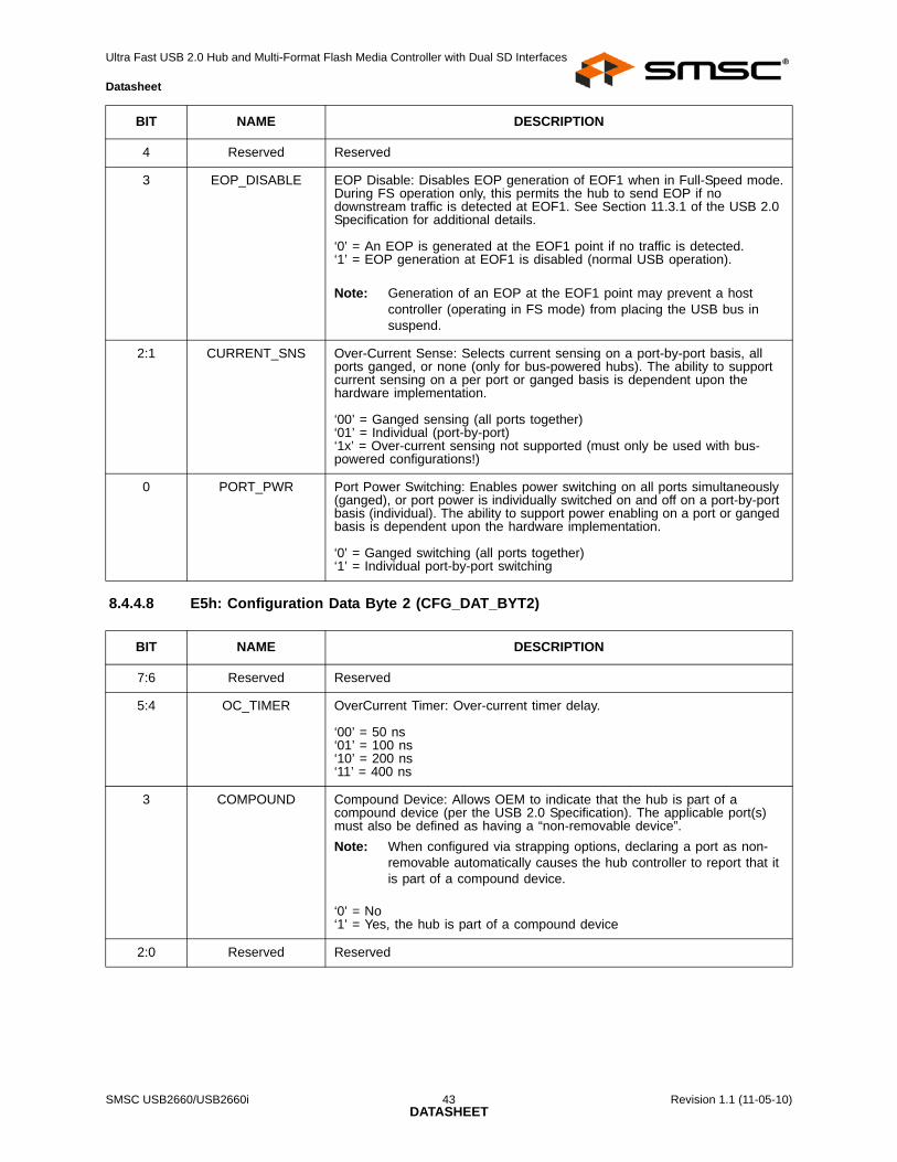
8.4.4.8 E5h: Configuration Data Byte 2 (CFG_DAT_BYT2)
4 Reserved Reserved
3 EOP_DISABLE EOP Disable: Disables EOP generation of EOF1 when in Full-Speed mode.During FS operation only, this permits the hub to send EOP if no downstream traffic is detected at EOF1. See Section 11.3.1 of the USB 2.0 Specification for additional details.
‘0’ = An EOP is generated at the EOF1 point if no traffic is detected.‘1’ = EOP generation at EOF1 is disabled (normal USB operation).
Note: Generation of an EOP at the EOF1 point may prevent a host controller (operating in FS mode) from placing the USB bus in suspend.
2:1 CURRENT_SNS Over-Current Sense: Selects current sensing on a port-by-port basis, all ports ganged, or none (only for bus-powered hubs). The ability to support current sensing on a per port or ganged basis is dependent upon the hardware implementation.
‘00’ = Ganged sensing (all ports together)‘01’ = Individual (port-by-port)‘1x’ = Over-current sensing not supported (must only be used with bus-powered configurations!)
0 PORT_PWR Port Power Switching: Enables power switching on all ports simultaneously (ganged), or port power is individually switched on and off on a port-by-port basis (individual). The ability to support power enabling on a port or ganged basis is dependent upon the hardware implementation.
3 COMPOUND Compound Device: Allows OEM to indicate that the hub is part of a compound device (per the USB 2.0 Specification). The applicable port(s) must also be defined as having a “non-removable device”.Note: When configured via strapping options, declaring a port as non-
removable automatically causes the hub controller to report that it is part of a compound device.
‘0’ = No‘1’ = Yes, the hub is part of a compound device
2:0 Reserved Reserved
BIT NAME DESCRIPTION
Ultra Fast USB 2.0 Hub and Multi-Format Flash Media Controller with Dual SD Interfaces
8.4.4.9 E6h: Configuration Data Byte 3 (CFG_DAT_BYT3)
8.4.4.10 E7h: Non-Removable Device
BIT NAME DESCRIPTION
7:4 Reserved Reserved
3 PRTMAP_EN Port Mapping Enable: Selects the method used by the hub to assign port numbers and disable ports.
‘0’ = Standard Mode. Strap options or the following registers are used to define which ports are enabled, and the ports are mapped as port ‘n’ on the hub is reported as port ‘n’ to the host, unless one of the ports is disabled, then the higher numbered ports are remapped in order to report contiguous port numbers to the host.
Register 300Ah: Port disable for self-powered operation (Reset = 0x00).Register 300Bh: Port disable for bus-powered operation (Reset = 0x00).
‘1’ = Port Map mode. The mode enables remapping via the registers defined below.
Register 30FBh: Port Map 12 (Reset = 0x00)Register 30FCh: Port Map 3 (Reset = 0x00)
2:0 Reserved Reserved
BIT BYTE NAME DESCRIPTION
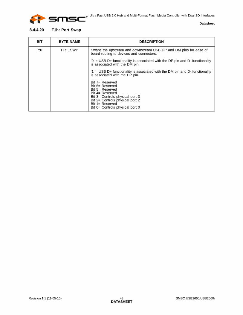
7:0 NR_DEVICE Indicates which port(s) include non-removable devices.
‘0’ = Port is removable‘1’ = Port is non-removable
Informs the host if one of the active ports has a permanent device that is undetachable from the hub. The device must provide its own descriptor data.
When using the internal default option, the NON_REM[1:0] pins will designate the appropriate ports as being non-removable.
Bit 7= ReservedBit 6= ReservedBit 5= ReservedBit 4= ReservedBit 3= Controls physical port 3Bit 2= Controls physical port 2Bit 1= Controls physical port 1 Bit 0= Reserved
Note: Bit 1 must be set to a ‘1’ by the firmware for proper identification of the card reader as a non-removable device.
Ultra Fast USB 2.0 Hub and Multi-Format Flash Media Controller with Dual SD Interfaces
8.4.4.11 E8h: Port Disable For Self-Powered Operation
8.4.4.12 E9h: Port Disable For Bus-Powered Operation
BIT BYTE NAME DESCRIPTION
7:0 PORT_DIS_SP Disables 1 or more ports.
‘0’ = Port is available‘1’ = Port is disabled
During self-powered operation this register selects the ports which will be permanently disabled. The ports are unavailable to be enabled or enumerated by a host controller. The ports can be disabled in any order since the internal logic will automatically report the correct number of enabled ports to the USB host and will reorder the active ports in order to ensure proper function.
Bit 7= ReservedBit 6= ReservedBit 5= ReservedBit 4= ReservedBit 3= Controls physical port 3Bit 2= Controls physical port 2Bit 1= Controls physical port 1Bit 0= Reserved
BIT BYTE NAME DESCRIPTION
7:0 PORT_DIS_BP Disables 1 or more ports.
‘0’ = Port is available‘1’ = Port is disabled
During self-powered operation, this register selects the ports which will be permanently disabled. The ports are unavailable to be enabled or enumerated by a host controller. The ports can be disabled in any order, the internal logic will automatically report the correct number of enabled ports to the USB host and will reorder the active ports in order to ensure proper function.
When using the internal default option, the PRT_DIS[1:0] pins will disable the appropriate ports.
Bit 7= ReservedBit 6= ReservedBit 5= ReservedBit 4= ReservedBit 3= Controls physical port 3Bit 2= Controls physical port 2Bit 1= Controls physical port 1Bit 0 is Reserved
Ultra Fast USB 2.0 Hub and Multi-Format Flash Media Controller with Dual SD Interfaces
8.4.4.13 EAh: Max Power For Self-Powered Operation
8.4.4.14 EBh: Max Power For Bus-Powered Operation
8.4.4.15 ECh: Hub Controller Max Current For Self-Powered Operation
8.4.4.16 EDh: Hub Controller Max Current For Bus-Powered Operation
BIT BYTE NAME DESCRIPTION
7:0 MAX_PWR_SP Value in 2 mA increments that the hub consumes from an upstream port (VBUS) when operating as a self-powered hub. This value includes the hub silicon along with the combined power consumption (from VBUS) of all associated circuitry on the board. This value also includes the power consumption of a permanently attached peripheral if the hub is configured as a compound device, and the embedded peripheral reports 0 mA in its descriptors.Note: The USB 2.0 Specification does not permit this value to exceed 100
mA.
BIT BYTE NAME DESCRIPTION
7:0 MAX_PWR_BP Value in 2 mA increments that the hub consumes from an upstream port (VBUS) when operating as a bus-powered hub. This value includes the hub silicon along with the combined power consumption (from VBUS) of all associated circuitry on the board. This value also includes the power consumption of a permanently attached peripheral if the hub is configured as a compound device, and the embedded peripheral reports 0 mA in its descriptors.
BIT BYTE NAME DESCRIPTION
7:0 HC_MAX_C_SP Value in 2 mA increments that the hub consumes from an upstream port (VBUS) when operating as a self-powered hub. This value includes the hub silicon along with the combined power consumption (from VBUS) of all associated circuitry on the board. This value does NOT include the power consumption of a permanently attached peripheral if the hub is configured as a compound device.Note: The USB 2.0 Specification does not permit this value to exceed 100
mA.
A value of 50 (decimal) indicates 100 mA, which is the default value.
BIT BYTE NAME DESCRIPTION
7:0 HC_MAX_C_BP Value in 2 mA increments that the hub consumes from an upstream port (VBUS) when operating as a bus-powered hub. This value will include the hub silicon along with the combined power consumption (from VBUS) of all associated circuitry on the board. This value will NOT include the power consumption of a permanently attached peripheral if the hub is configured as a compound device.
A value of 50 (decimal) would indicate 100 mA, which is the default value.
Ultra Fast USB 2.0 Hub and Multi-Format Flash Media Controller with Dual SD Interfaces
7:0 PWR_ON_TIME The length of time that it takes (in 2 ms intervals) from the time the host initiated power-on sequence begins on a port until power is adequate on that port. If the host requests the power-on time, the system software uses this value to determine how long to wait before accessing a powered-on port.
BIT NAME DESCRIPTION
7:2 Reserved Reserved
1:0 BOOST_IOUT USB electrical signaling drive strength boost bit for the upstream port ‘A’.
‘00’ = Normal electrical drive strength = No boost‘01’ = Elevated electrical drive strength = Low (approximately 4% boost)‘10’ = Elevated electrical drive strength = Medium (approximately 8% boost)‘11’ = Elevated electrical drive strength = High (approximately 12% boost)
Note: “Boost” could result in non-USB compliant parameters. OEM should use a ‘00’ value unless specific implementation issues require additional signal boosting to correct for degraded USB signaling levels.
BIT NAME DESCRIPTION
7:6 Reserved Reserved
5:4 BOOST_IOUT_3 Upstream USB electrical signaling drive strength boost bit for downstream port ‘3’.
‘00’ = Normal electrical drive strength = No boost‘01’ = Elevated electrical drive strength = Low (approximately 4% boost)‘10’ = Elevated electrical drive strength = Medium (approximately 8% boost)‘11’ = Elevated electrical drive strength = High (approximately 12% boost)
3:2 BOOST_IOUT_2 Upstream USB electrical signaling drive strength boost bit for downstream port ‘2’.
‘00’ = Normal electrical drive strength = No boost‘01’ = Elevated electrical drive strength = Low (approximately 4% boost)‘10’ = Elevated electrical drive strength = Medium (approximately 8% boost)‘11’ = Elevated electrical drive strength = High (approximately 12% boost)Note: “Boost” could result in non-USB Compliant parameters. OEM
should use a ‘00’ value unless specific implementation issues require additional signal boosting to correct for degraded USB signaling levels.
1:0 Reserved Always reads ‘0’.
Ultra Fast USB 2.0 Hub and Multi-Format Flash Media Controller with Dual SD Interfaces
When a hub is enumerated by a USB host controller, the hub is only permitted to report how many ports it has; the hub is not permitted to select a numerical range or assignment. The host controller will number the downstream ports of the hub starting with the number '1', up to the number of ports that the hub reported having.
The host's port number is referred to as “logical port number” and the physical port on the hub is the “physical port number”. When remapping mode is enabled (see PRTMAP_EN in Register 08h: Configuration Data Byte 3) the hub's downstream port numbers can be remapped to different logical port numbers (assigned by the host).
Note: The OEM must ensure that contiguous logical port numbers are used, starting from number ‘1’ up to the maximum number of enabled ports; this ensures that the hub's ports are numbered in accordance with the way a host will communicate with the ports.
Table 8.5 Port Map Register for Ports 1 & 2
Bit [7:4] ‘0000’ Physical port 2 is disabled
‘0001’ Physical port 2 is mapped to Logical port 1
‘0010’ Physical port 2 is mapped to Logical port 2
‘0011’ Physical port 2 is mapped to Logical port 3
‘0100’to
‘1111’
Illegal; Do not use
Bit [3:0] ‘0000’ Physical port 1 is disabled
‘0001’ Physical port 1 is mapped to Logical port 1
‘0010’ Physical port 1 is mapped to Logical port 2
‘0011’ Physical port 1 is mapped to Logical port 3
‘0100’to
‘1111’
Illegal; Do not use
Ultra Fast USB 2.0 Hub and Multi-Format Flash Media Controller with Dual SD Interfaces
When a hub is enumerated by a USB host controller, the hub is only permitted to report how many ports it has; the hub is not permitted to select a numerical range or assignment. The host controller will number the downstream ports of the hub starting with the number '1', up to the number of ports that the hub reported having.
The host's port number is referred to as “logical port number” and the physical port on the hub is the “physical port number”. When remapping mode is enabled (see PRTMAP_EN in Register 08h: Configuration Data Byte 3) the hub's downstream port numbers can be remapped to different logical port numbers (assigned by the host).
Note: The OEM must ensure that contiguous logical port numbers are used, starting from number ‘1’ up to the maximum number of enabled ports; this ensures that the hub's ports are numbered in accordance with the way a host will communicate with the ports.
BYTE BYTE NAME DESCRIPTION
6:0 Reserved Reserved.
BIT BYTE NAME DESCRIPTION
7:0 Not Applicable Not applicable.
Table 8.6 Port Map Register for Port 3
Bit [7:4] ‘0000’ Reserved
‘0001’ Reserved
‘0010’ Reserved
‘0011’ Reserved
‘0100’to
‘1111’
Illegal; Do not use
Bit [3:0] ‘0000’ Physical port 3 is disabled
‘0001’ Physical port 3 is mapped to Logical port 1
‘0010’ Physical port 3 is mapped to Logical port 2
‘0011’ Physical port 3 is mapped to Logical port 3
‘0100’to
‘1111’
Illegal; Do not use
Ultra Fast USB 2.0 Hub and Multi-Format Flash Media Controller with Dual SD Interfaces
8.4.5 Internal Flash Media Controller Extended Configurations
Enable Registers 100h - 17Fh by setting bit 7 of bmAttribute.
8.4.5.1 100h-106h: Combo LUN 0 Identifier String
8.4.5.2 107h-10Dh: Combo LUN 1 Identifier String
8.4.5.3 10Eh-114h: Combo LUN 2 Identifier String
8.4.5.4 115h-11Bh: Combo LUN 3 Identifier String
8.4.5.5 11Ch-122h: Combo LUN 4 Identifier String
BYTE NAME DESCRIPTION
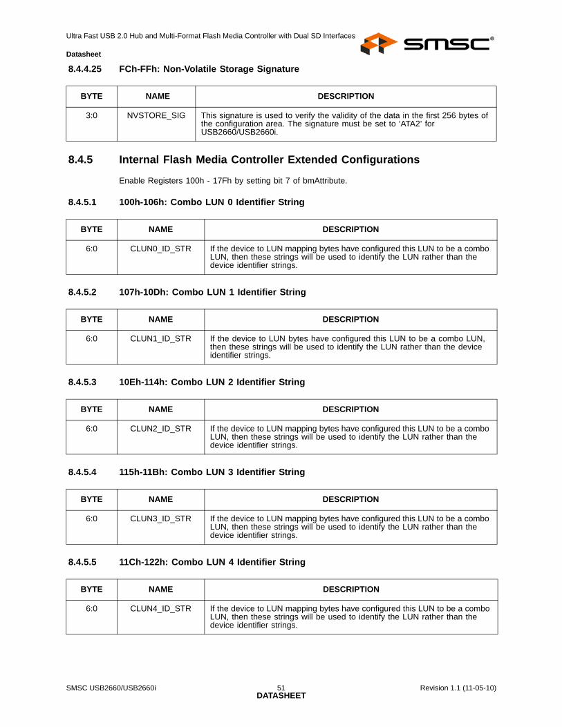
3:0 NVSTORE_SIG This signature is used to verify the validity of the data in the first 256 bytes of the configuration area. The signature must be set to ‘ATA2’ for USB2660/USB2660i.
BYTE NAME DESCRIPTION
6:0 CLUN0_ID_STR If the device to LUN mapping bytes have configured this LUN to be a combo LUN, then these strings will be used to identify the LUN rather than the device identifier strings.
BYTE NAME DESCRIPTION
6:0 CLUN1_ID_STR If the device to LUN bytes have configured this LUN to be a combo LUN, then these strings will be used to identify the LUN rather than the device identifier strings.
BYTE NAME DESCRIPTION
6:0 CLUN2_ID_STR If the device to LUN mapping bytes have configured this LUN to be a combo LUN, then these strings will be used to identify the LUN rather than the device identifier strings.
BYTE NAME DESCRIPTION
6:0 CLUN3_ID_STR If the device to LUN mapping bytes have configured this LUN to be a combo LUN, then these strings will be used to identify the LUN rather than the device identifier strings.
BYTE NAME DESCRIPTION
6:0 CLUN4_ID_STR If the device to LUN mapping bytes have configured this LUN to be a combo LUN, then these strings will be used to identify the LUN rather than the device identifier strings.
Ultra Fast USB 2.0 Hub and Multi-Format Flash Media Controller with Dual SD Interfaces
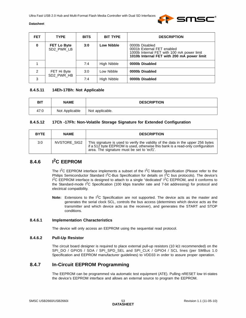
8.4.5.10 14Ch-14Dh: Second Secure Digital Device Power Configuration
The device has two internal FETs which can be utilized for card power. For information about the otherinternal FET, please see Section 8.4.2.3, "A4h-A5h: Smart Media Device Power Configuration," onpage 39. The settings are stored in NVSTORE. This section describes the default internalconfiguration.
1. A card can be powered by an external FET or by an internal FET.
2. The power limit can be set to 100 mA or 200 mA (Default) for the internal FET.
Each media uses two bytes to store its device power configuration. Bit 3 selects between internal orexternal card power FET options. For internal FET card power control, bits 0 through 2 are used toset the power limit. The “Device Power Configuration” bits are ignored unless the “Enable DevicePower Configuration” bit is set. See Section 8.4.1.19, "9Ch-9Fh: Attribute Byte Descriptions," onpage 37.
BYTE NAME DESCRIPTION
6:0 DEV4_ID_STR This ID string is associated with the second Secure Digital / MultiMediaCard “SD/MMC2” device.
BYTE NAME DESCRIPTION
21:0 Not Applicable Not applicable.
BIT NAME DESCRIPTION
7:0 DYN_NUM_EXT_LUN
These bytes are used to specify the number of LUNs the device exposes to the host. These bytes are also used for icon sharing by assigning more than one LUN to a single icon. This is used in applications where the device utilizes a combo socket and the OEM wishes to have only a single icon displayed for one or more interfaces.
If this field is set to "FF", the program assumes that you are using the default value and icons will be configured per the default configuration.
BYTE NAME DESCRIPTION
4:0 DEV_LUN_MAP These registers map a device controller (SD/MMC, SM (Note 8.2), and MS) to a Logical Unit Number (LUN). The device reports the mapped LUNs to the USB host in the USB descriptor during enumeration. The icon installer associates custom icons with the LUNs specified in these fields.
Setting a register to "FF" indicates that the device is not mapped. Setting all of the DEV_LUN_MAP registers for all devices to "FF" forces the use of the default mapping configuration. Not all configurations are valid. Valid configurations depend on the hardware, packaging, and OEM board layout. The number of unique LUNs mapped must match the value in the Section 8.4.3.7, "D3h: Dynamic Number of LUNs," on page 41.
Ultra Fast USB 2.0 Hub and Multi-Format Flash Media Controller with Dual SD Interfaces
8.4.5.12 17Ch -17Fh: Non-Volatile Storage Signature for Extended Configuration
8.4.6 I2C EEPROM
The I2C EEPROM interface implements a subset of the I2C Master Specification (Please refer to thePhilips Semiconductor Standard I2C-Bus Specification for details on I2C bus protocols). The device’sI2C EEPROM interface is designed to attach to a single “dedicated” I2C EEPROM, and it conforms tothe Standard-mode I2C Specification (100 kbps transfer rate and 7-bit addressing) for protocol andelectrical compatibility.
Note: Extensions to the I2C Specification are not supported. The device acts as the master andgenerates the serial clock SCL, controls the bus access (determines which device acts as thetransmitter and which device acts as the receiver), and generates the START and STOPconditions.
8.4.6.1 Implementation Characteristics
The device will only access an EEPROM using the sequential read protocol.
8.4.6.2 Pull-Up Resistor
The circuit board designer is required to place external pull-up resistors (10 kΩ recommended) on theSPI_DO / GPIO5 / SDA / SPI_SPD_SEL and SPI_CLK / GPIO4 / SCL lines (per SMBus 1.0Specification and EEPROM manufacturer guidelines) to VDD33 in order to assure proper operation.
8.4.7 In-Circuit EEPROM Programming
The EEPROM can be programmed via automatic test equipment (ATE). Pulling nRESET low tri-statesthe device’s EEPROM interface and allows an external source to program the EEPROM.
FET TYPE BITS BIT TYPE DESCRIPTION
0 FET Lo ByteSD2_PWR_LB
3:0 Low Nibble 0000b Disabled0001b External FET enabled1000b Internal FET with 100 mA power limit1010b Internal FET with 200 mA power limit
1 7:4 High Nibble 0000b Disabled
2 FET Hi ByteSD2_PWR_HB
3:0 Low Nibble 0000b Disabled
3 7:4 High Nibble 0000b Disabled
BIT NAME DESCRIPTION
47:0 Not Applicable Not applicable.
BYTE NAME DESCRIPTION
3:0 NVSTORE_SIG2 This signature is used to verify the validity of the data in the upper 256 bytes if a 512 byte EEPROM is used, otherwise this bank is a read-only configuration area. The signature must be set to 'ecf1'.
Ultra Fast USB 2.0 Hub and Multi-Format Flash Media Controller with Dual SD Interfaces
8.5 Default Configuration OptionThe SMSC device can be configured via its internal default configuration. Please see Section 8.3.2,"EEPROM Data Descriptor" for specific details on how to enable default configuration. Please refer toTable 8.1 for the internal default values that are loaded when this option is selected.
8.5.1 External Hardware nRESET
A valid hardware reset is defined as assertion of nRESET for a minimum of 1 μs after all powersupplies are within operating range. While reset is asserted, the device (and its associated externalcircuitry) consumes less than 500 μA of current from the upstream USB power source.
Assertion of nRESET (external pin) causes the following:
1. All downstream ports are disabled and PRTCTL power to downstream devices is removed.
2. The PHYs are disabled and the differential pairs will be in a high-impedance state.
3. All transactions immediately terminate; no states are saved.
4. All internal registers return to the default state (in most cases, 00h).
5. The external crystal oscillator is halted.
6. The PLL is halted.
8.5.1.1 nRESET for EEPROM Configuration
Figure 8.1 nRESET Timing for EEPROM Mode
Table 8.7 nRESET Timing for EEPROM Mode
NAME DESCRIPTION MIN TYP MAX UNITS
t1 nRESET asserted 1 μsec
t2 Device recovery/stabilization 500 μsec
t3 8051 programs device configuration 20 50 msec
t4 USB attach (See Note) 100 msec
t5 Host acknowledges attach and signals USB reset 100 msec
t6 USB idle Undefined msec
t7 Completion time for requests (with or without data stage)
5 msec
t1 t2t4
t5 t6 t7
nRESET
VSS
Hardware reset
asserted
Device Recovery/
Stabilization
8051 Sets Configuration
Registers
Attach USB
Upstream
USB Reset recovery Idle
Start completion
request response
t3
Ultra Fast USB 2.0 Hub and Multi-Format Flash Media Controller with Dual SD Interfaces
Note: All power supplies must have reached the operating levels mandated in Chapter 10, DCParameters, prior to (or coincident with) the assertion of nRESET.
8.5.2 USB Bus Reset
In response to the upstream port signaling a reset to the device, the device does the following:
Note: The device does not propagate the upstream USB reset to downstream devices.
1. Sets default address to ‘0’.
2. Sets configuration to: Unconfigured.
3. Negates PRTCTL[3:2] to all downstream ports.
4. Clears all TT buffers.
5. Moves device from suspended to active (if suspended).
6. Complies with Section 11.10 of the USB 2.0 Specification for behavior after completion of the resetsequence.
The host then configures the device and the device’s downstream port devices in accordance with theUSB 2.0 Specification.
Ultra Fast USB 2.0 Hub and Multi-Format Flash Media Controller with Dual SD Interfaces
9.1 Oscillator/CrystalParallel Resonant, Fundamental Mode, 24 MHz ± 350 ppm.
Figure 9.1 Typical Crystal Circuit
Table 9.1 Crystal Circuit Legend
Figure 9.2 Capacitance Formulas
Note 9.1 C0 is usually included (subtracted by the crystal manufacturer) in the specification for CLand should be set to ‘0’ for use in the calculation of the capacitance formulas in Figure 9.2,"Capacitance Formulas". However, the OEM PCB itself may present a parasiticcapacitance between XTAL1 and XTAL2. For an accurate calculation of C1 and C2, takethe parasitic capacitance between traces XTAL1 and XTAL2 into account.
Note 9.2 Each of these capacitance values is typically approximately 18 pF.
SYMBOL DESCRIPTION IN ACCORDANCE WITH
C0 Crystal shunt capacitanceCrystal manufacturer’s specification (See Note 9.1)
CL Crystal load capacitance
CB Total board or trace capacitance
OEM board design
CS Stray capacitance SMSC IC and OEM board design
CXTAL XTAL pin input capacitance SMSC IC
C1 Load capacitors installed on OEM board
Calculated values based on Figure 9.2, "Capacitance Formulas" (See Note 9.2)C2
C1 = 2 x (CL – C0) – CS1
C2 = 2 x (CL – C0) – CS2
Ultra Fast USB 2.0 Hub and Multi-Format Flash Media Controller with Dual SD Interfaces
The external clock is recommended to conform to the signaling level designated in the JESD76-2specification on 1.8 V CMOS Logic. XTAL2 should be treated as a no connect.
9.3.1 I2C EEPROM
Frequency is fixed at 58.6 kHz ± 20%
9.3.2 USB 2.0
The SMSC device conforms to all voltage, power, and timing characteristics and specifications as setforth in the USB 2.0 Specification. Please refer to the USB 2.0 Specification for more information.
Ultra Fast USB 2.0 Hub and Multi-Format Flash Media Controller with Dual SD Interfaces
Note: Stresses above the specified parameters may cause permanent damage to the device. This isa stress rating only. Functional operation of the device at any condition above those indicatedin the operation sections of this specification is not implied. When powering this device fromlaboratory or system power supplies the absolute maximum ratings must not be exceeded ordevice failure can result. Some power supplies exhibit voltage spikes on their outputs when theAC power is switched on or off. In addition, voltage transients on the AC power line may appearon the DC output. When this possibility exists, a clamp circuit should be used.
Figure 10.1 Supply Rise Time Model
PARAMETER SYMBOL MIN MAX UNITS COMMENTS
Storage Temperature
TSTOR -55 150 °C
Lead Temperature
°C Please refer to JEDEC specification J-STD-020D.
3.3 V supply voltage
VDD33 -0.5 4.0 V
Voltage on USB+ and USB- pins
-0.5 (3.3 V supply voltage + 2) ≤ 6 V
Voltage on GPIO8 and GPIO10
-0.5 VDD33 + 0.3 V When internal power FET operation of these pins are enabled, these pins may be simultaneously shorted to ground or any voltage up to 3.63 V indefinitely, without damage to the device as long as VDD33 is less than 3.63 V and TA is less than 70oC.
Voltage on any signal pin
-0.5 VDD33 + 0.3 V
Voltage on XTAL1
-0.5 3.6 V
Voltage on XTAL2
-0.5 2.0 V
t10%
10%
90%
Voltage tRT
t90% Time
100%3.3 V
VSS
VDD33
Ultra Fast USB 2.0 Hub and Multi-Format Flash Media Controller with Dual SD Interfaces
3.3 V supply voltage VDD33 3.0 3.6 V A 3.3 V regulator with an output tolerance of 1% must be used if the output of the internal power FET’s must support a 5% tolerance.
3.3 V supply rise time tRT 0 400 μs (Figure 10.1)
Voltage on USB+ and USB- pins
-0.3 5.5 V If any 3.3 V supply voltage drops below 3.0 V, then the MAX becomes:
(3.3 V supply voltage) + 0.5 ≤ 5.5
Voltage on any signal pin
-0.3 VDD33 V
Voltage on XTAL1 -0.3 2.0 V
Voltage on XTAL2 -0.3 2.0 V
PARAMETER SYMBOL MIN TYP MAX UNITS COMMENTS
I, IPU, IPD Type Input Buffer
Low Input Level
High Input Level
Pull Down
Pull Up
VILI
VIHI
PD
PU
2.0
72
58
0.8 V
V
μA
μA
TTL Levels
IS Type Input Buffer
Low Input Level
High Input Level
Hysteresis
VILI
VIHI
VHYSI
2.0
420
0.8 V
V
mV
TTL Levels
Ultra Fast USB 2.0 Hub and Multi-Format Flash Media Controller with Dual SD Interfaces
Note 10.1 Output leakage is measured with the current pins in high impedance.
Note 10.2 See the USB 2.0 Specification, Chapter 7, for USB DC electrical characteristics
Note 10.3 RBIAS is a 3.3 V tolerant analog pin.
Note 10.4 Output current range is controlled by program software. The software disables the FETduring short circuit condition.
Note 10.5 Typical and maximum values were characterized using the following temperature ranges:The USB2660 supports the commercial temperature range of 0°C to +70°CThe USB2660i supports the industrial temperature range of -40°C to +85°C
Supply Current Unconfigured
Hi-Speed Host
USB2660USB2660i
Full Speed Host
USB2660USB2660i
ICCINTHSICCINTHS
ICCINITFSICCINITFS
7070
6565
8080
7575
mAmA
mAmA
Note 10.5
Supply Current ConfiguredHi-Speed Host, 1 downstream port
USB2660USB2660i
IHCH1IHCH1
260260
270275
mAmA
(Note 10.5)
Supply Current ConfiguredHi-Speed Host, each additional downstream port
USB2660USB2660i
2525
3035
mAmA
Supply Current ConfiguredFull-Speed Host, 1 downstream port
USB2660USB2660i
IFCC1IFCC1
200200
210215
mAmA
Supply Current ConfiguredFull-Speed Host, each additional downstream port
USB2660USB2660i
2020
2525
mAmA
Supply Current Suspend
USB2660USB2660i
ICSBYICSBY
500500
9501200
µAµA
(Note 10.5)
Supply Current Reset
USB2660USB2660i
IRSTIRST
230230
700900
µAµA
PARAMETER SYMBOL MIN TYP MAX UNITS COMMENTS
Ultra Fast USB 2.0 Hub and Multi-Format Flash Media Controller with Dual SD Interfaces