19
1 LANDYNE 蓝带软件 User Manual Simulation and Analysis of Electron Diffraction Pattern Copyright 2011-2021 LANDYNE © All Right Reserved

1
LANDYNE蓝带软件
User Manual
Simulation and Analysis of Electron Diffraction Pattern
Copyright 2011-2021 LANDYNE ©
All Right Reserved

2
Contents 1. Introduction ............................................................................................................................................... 3 2. Theory background ................................................................................................................................... 4
2.1 Electron diffraction geometry and intensity ........................................................................................ 4 2.2 Electron diffraction of twins and coexisted multiple phases ............................................................... 4 2.3 Determination of a zone axis and indexing ......................................................................................... 5
3. The graphic user interface of SAED ......................................................................................................... 5 3.1 Main interface ..................................................................................................................................... 5 3.2 Menu and toolbar ................................................................................................................................ 6
4. Usage of SAED ......................................................................................................................................... 7 4.1 Prepare a new data file ....................................................................................................................... 8 4.2 Simulation ........................................................................................................................................... 9 4.2 Save figure for publication .................................................................................................................. 9 4.4 Determination of zone axis and indexing .......................................................................................... 11
5. Special topics on SAED .......................................................................................................................... 12 5.1 Partial occupancy factor and isotropic temperature factor.............................................................. 13 5.2 Load and shift EDP ........................................................................................................................... 13 5.3 Determination of weight ratio of a multiple-phase system ............................................................... 13 5.4 Simulation of twins and coexisted multiple phases ........................................................................... 13
6. Examples ................................................................................................................................................. 14 6.1 Pt-Bi thin film .................................................................................................................................... 14 6.2 Cu2S nanofiber .................................................................................................................................. 15
7. Related programs: SVAT, SAKI, SPICA, and PCED ............................................................................ 18 7.1 SVAT ................................................................................................................................................ 18 7.2 SAKI ................................................................................................................................................. 18 7.3 SPICA ............................................................................................................................................... 19 7.4 PCED ................................................................................................................................................ 19
3
1. Introduction
Selected area electron diffraction analysis has been extensively used in materials science for
phase identification, determination of structural intergrowth and growth directions, e.g. twin
relation and fixed orientation of co-existing multiple phases.
Due to a much stronger interaction of electrons with matter compared to X-rays, electron
diffraction has non-negligible advantages and disadvantage in comparison with X-ray diffraction.
On one hand, nano-objects that are too small for conventional X-ray diffraction experiment and
would have to be taken to a synchrotron can be studied in the laboratory by electron diffraction.
Moreover, electron diffraction patterns can show reflections corresponding to a resolution
beyond that available with X-rays for light atoms. On the other hand, the much stronger
interaction of electrons with matter as well as very small diffraction angles also cause strong
dynamical diffraction effects, such as multiple diffraction, which hinder structural interpretation
of electron diffraction patterns.
Simulation of electron diffraction patterns plays a vital role in interpreting experimental results.
Electron diffraction patterns from a single crystal grain and a polycrystalline sample are common
in essence but different in many aspects, so we treat the two cases separately for advanced
simulation and analysis of electron diffraction patterns. PCED4 is for selected-area electron
diffraction patterns of polycrystalline samples. SAED is for selected-area electron diffraction
patterns of single-crystal samples.
Software current available for simulation of electron diffraction is primarily designed for a
single-phase only. For advanced simulation and analysis of electron diffraction patterns, the
functionalities in such software are not enough, for example, in the analyses of twining,
coexisted multiple phases with a fixed orientation, and the comparison of two similar diffraction
patterns from different phases. A practical task in electron diffraction analysis is to find the zone
axis of the diffraction pattern and indexing; such an analysis can be used for phase identification,
the orientation of a crystal grain, et cetera. A projected atomic potential (difference) map can be
used to interpret the HREM structural image and improve a structural model; the tasks are
treated as an extension in PAPM. Thus, we have developed SAED; the current version is 5.
Previous version:
JECP/ED: Journal of Applied Crystallography, 36 (2003) 956
SAED2: Proceedings of Microscopy & Microanalysis, 18 S2 (2012) 1262.
SAED3: Microscopy and Analysis, 2019 (May issue 16-19).
The features in SAED are briefly listed here,
1. A window frame with a panel is used to show the simulated pattern or match the
preloaded experimental diffraction pattern.
2. Input parameters for the calculation can be initialized with an operational panel and
several dialog windows.
3. Input structure data files can be easily prepared using a computer assistant.

4
4. Multiple phases can be loaded and calculated simultaneously to simulate the diffraction
patterns for twins, coexisted phases with a fixed orientation, and for comparison of the
similar patterns from a different phase.
5. An experimental pattern can be aligned, resized, and rotated.
6. Label tools are available to prepare figures for publication.
SAED was written and compiled in Java 8. Further code optimization (including obfuscation)
was carried out for the compiled class files. A license file is needed to unlock the program
(SAED.jar) for loading input data files. A license is available from the LANDYNE computer
software.
2. Theory background
2.1 Electron diffraction geometry and intensity
The kinematical and dynamical theories of high-energy electron diffraction have been well
documented in the textbooks (e.g., Peng et al., 2004, other books on electron diffraction theory)
and literature references (e.g., Metherell, 1975).
The electron atom scatting factor can be derived from the X-ray atom scatter factor using the
Mott-Bethe relationship or directly obtained from a parameterized table of electron atom scatter
factors (Peng et al. 1996). Here we use the second method.
Following the electron diffraction geometry, the reciprocal length (R) of a reflection in a
diffraction pattern can be related to the length of the reciprocal vector g(hkl) as
𝑅 = 𝐿 (
𝑔
𝐾) (1 +
3
8
𝑔2
𝐾2)
(1)
where L is the camera length, g=|g(hkl)| and K is the wave vector of an incident electron beam,
K = |K|.
For high-energy electron diffraction, the Ewald sphere’s radius is relatively large; thus, the
electron diffraction pattern of the thin sample reveals the two-dimensional distribution of
reciprocal lattice points.
Electron diffraction intensity in kinematical theory is given by:
2
gg FI
(2)
Here Fg is the so-called structure factor.
In SAED, dynamical electron diffraction intensities are calculated using the Bloch wave method
(Metherell 1975). Readers should check the formulas in the original research papers.
2.2 Electron diffraction of twins and coexisted multiple phases
Based on their diffraction patterns, twinned crystals may be grouped into three general
categories. Non-merohedral twins have two or more crystalline domains with reciprocal lattices
that either do not overlap or only partially overlapped. In contrast, Merohedral twins have

5
domains with diffraction patterns that are completely overlapped. For merohedral twins, the
symmetry operations relating the twinned domains are part of the sample's Laue group but are
not a part of the space group. Pseudo-merohedral also has domains with completely overlapped
diffraction patterns, but the symmetry operation relating to the domains is not part of the
sample's Laue group.
Two phases or more may coexist with a fixed orientation relationship in a complex alloy system.
Electron diffraction analysis can be used to determine the orientation relationship. Precipitates
may have a fixed orientation with the matrix. To study the precipitates, it usually tilts the matrix
to get a particular orientation of the precipitates since the precipitates are small particles.
For twins and multiple coexisted phases, the electron diffraction pattern simulation requires to be
calculated based on multiple structures in one frame. SAED4 is designed to calculate the patterns
from multiple structures one by one and easily adjusted any patterns to simulate the patterns
from twins and multiple structures coexisted with a fixed orientation.
2.3 Determination of a zone axis and indexing
A practical task in electron diffraction analysis is to find the zone axis of the diffraction pattern
and indexing; such an analysis can be used for phase identification, the orientation of a crystal
grain, et cetera.
SAED provides tools to measure the scale bar and to measure two basic reciprocal vectors’
lengths and the angles between them on a diffraction pattern in jpeg or tiff format.
The two basic reciprocal vectors’ lengths are matched to all possible (hkl) with a given tolerance.
Then the angle between the two basic reciprocal vectors is checked, one of the zone axes with
the least mismatch values is listed out, and possible zone axes can be saved to a file.
Since only the tolerance of reciprocal lengths is defined in the Find Zone Axis dialog, the angle
is checked by the reciprocal length of the third edge in the triangle formed by the two basic
reciprocal vectors.
3. The graphic user interface of SAED
3.1 Main interface
The main interface of SAED4 is shown in Fig. 1. The usage of SAED for simulation needs to
load structure data and to set up input parameters, then click the Calculate button in
the Calculation control panel. The usage of SAED for zone axis search or phase identification
needs to load experimental diffraction pattern first and then find zone axis and then match the
calculated patterns by chosen structure data and input parameters. Multiple structure data can
load simultaneously for comparison or simulation of various twins and coexisted structures with
a fixed orientation.

6
Figure 1. Snap-shot of the main panels in SAED, a simulation of an
electron diffraction pattern of Aluminum along [001] zone axis.
3.2 Menu and toolbar
Menu and toolbar can be used to pop up dialogs for loading data or changing parameters. The
menu gives more text descriptions and organized in groups, while the toolbar shows in graphics
and easy access.
Crystal menu provides an interface for creating the new structure data, loading the input
structure (the same structure can reload for twins), and clearing all the loaded structures except
the default (Al) structure.
Experiment menu provides an interface for loading experimental electron diffraction pattern
(EDP) in JPEG and TIFF format. The loaded SAED pattern (image) can be set in inversed
contrast or cleanup. The image can be resized and rotated and shifted/centered by drag-and-drop
action, referring to a set of concentric circles and lines. Loading image by drag-and-drop:
selecting an image file by the mouse pointer, press down the left button of the mouse, drop to the
drop-box icon on the menu bar, and release the left button of the mouse. Reciprocal spacing
marker provides a tool to make the scale calibration using the scale bar in the SAED pattern.

7
When the position of the image is set up, close the Image Operation dialog; Find [uvw]
provides a dialog for calibrating the matching-factor, finding the basic reciprocal vectors of the
EDP, and finding the [uvw]. A zone axis with the least mismatching residue is shown, and
detailed info on a list of all possible zone axes can be saved to a text file.
Simulation menu provides a submenu for the choice of theories between kinematical and
dynamical diffraction theories. The default choice is the kinematical diffraction theory. The
dynamical calculation may not be suitable for a crystal with a large unit cell since it will take a
very long time in the Bloch wave method. The high voltage of the microscope and the maximum
of the index number for the calculation can be set up. A dialog window for adjusting the pattern
zoom and intensity scale simulates the camera length and exposure time and a dialog window for
selecting the label of diffraction spots (reflections). The label on reflections can be used to select
the scheme for index and intensity. Weak diffraction spots can be rescaled to a constant, or it can
also be chosen to show reciprocal lattice only.
Pattern menu provides a dialog for ROI and PPI; the simulated patterns can be saved as output
files in JPEG or TIFF format.
Table menu provides a periodic table of elements and a table of the space group.
Option menu provides freedom of customizing the appearance of SAED (look and feel skin), a
switch to show or hide the graphic menu bar and set up the default position and the size of the
panels.
Figure 2. Snap-shot of the supporting panels in SAED for analysis of experimental SAED
patterns.

8
Figure 3. Snap-shot of the adjustment panel in SAED for simulation of calculated SAED patterns.
Help menu can be used to find the current drive and the serial number (SN), which is required
for license files, a version, and license information.
The toolbar provides a quick way to access conveniently the functions described above. The
toolbar can be switch on/off. The functions of the toolbar are shown by both the icon image and
tooltip text. Most frequently used menus and submenus are listed in the Toolbar. Drag-and-drop
box only appears in the toolbar, allowing the drag and drop action to load an image in JPEG or
TIFF format quickly. A lock icon is unlocked when a valid license file is the same fold. Without
a license file, SAED can be evaluated in a trial model. Contact Landyne for purchasing the
license file.
4. Usage of SAED
To run SAED, a user may use (1) Landyne launcher or (2) double click the icon of SAED.jar or
(3) type: java -jar (-Xmx512m) SAED.jar in the command line. -Xmx512m is an option to locate
the memory of a Java virtual machine up to 512 MB. The main window frame and the control
interface of the program, similar to Fig. 1, will show up.
In the following, we show step by step from preparing structure data file, common routine usage
for simulation, and to the last steps of saving and printing the results. More details on specific
topics are left to the next section.
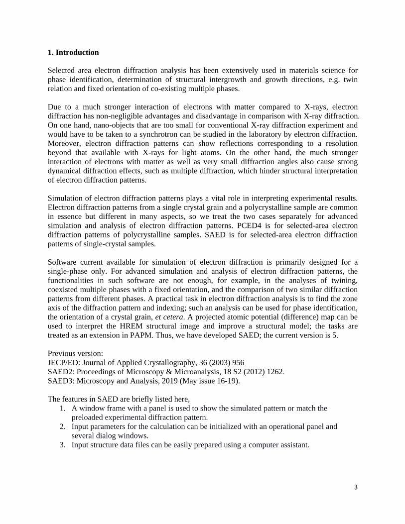
4. 1 Prepare new crystal structure file
A structure data file can be prepared using the New Crystal Structure File dialogue window in
Figure 4. The dialogue window provides an automatic assistant for the user and makes sure to
meet the requirement of the file format. The template is embedded with the 230 space groups in
the Hermann-Mauguin notation, which list in the international table for crystallography.
However, only b unique axis will be used in a monoclinic system. Two origin choices can be
accepted as input parameters, but choice-2 will be converted to choice-1. To save the data
structure, click the Save button; or make a new one click the New button.
The crystal file can be also converted from a previous data for modification or from a
crystallographic information file (CIF). If a data file in an alternative setting of space group for
triclinic, monoclinic and orthorhombic systems is used, please click on the alternative settings
9
(1~74). A tool for the transformation of files in the nonconventional notations to the standard
notations is provided.
Figure 4. Snap-shot of the preparation of the new crystal structure file.
4.2 Simulation
Kinematical diffraction theory (default selection) and dynamical diffraction of Bloch wave
theory are used in the simulation. Basic parameters for calculation, e.g., high voltage, pattern
zoom, and intensity scale, can be adjusted in the Simulation menu.
The calculation in Bloch wave theory may take time for a crystal structure with relative large
lattice parameters. In order to save the time, (i) the software provides an option for user to
terminate the calculation process when the result is good enough or continue the calculation, as
shown in Figure 5; (ii) the software will use previous calculated parameters to simulate a
diffraction pattern when only the thickness is changed.

10
Figure 5. Snap-shot of an option for user to terminate or continue the calculation.
A structure data for calculation should be selected in a list of loaded structure data. After
choosing the thickness, zone axis, tilt angles to generate a new diffraction pattern, needs to click
the Calculate button. The pattern can be adjusted by changing other parameters.
Mass proportion defines the same unit weight for all loaded structures as the default value.
Mass proportion is meaningful only when two or more structural data are calculated at a
composite diffraction pattern.
Orientation and mirror operation is used to orient the simulated pattern to match the
experimental pattern and generate various twins.
Diffraction Patterns can be viewed with four predefined shapes and in various colors. Pattern
(ZOLZ and FOLZ) can be displayed or hidden. Index and intensity can be labeled for basic
reciprocal vectors and for diffraction spots selected by the intensity level. Basic vectors and Laue
center can be displayed and hidden.
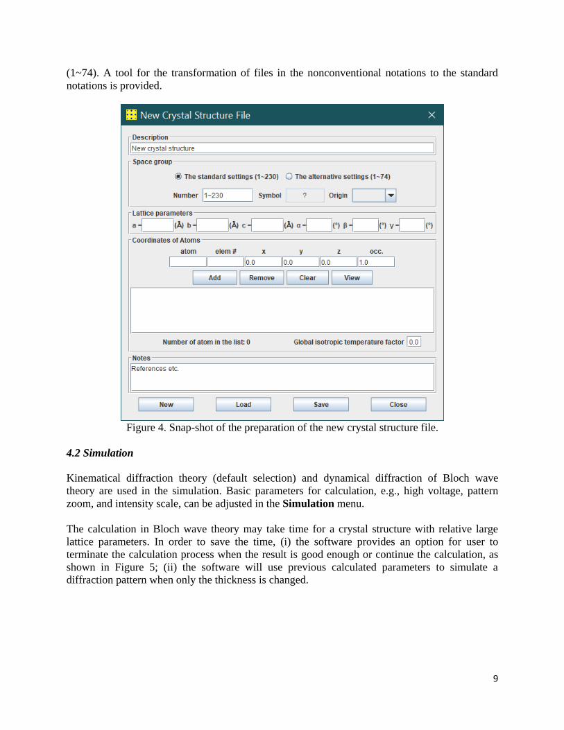
4.3 Sava figures for publication
Together with experimental images, these simulated patterns can be saved to images, which are
ready for publication. Figure 6 shows the tools of (a) region of interest, (b) index, (c) zone axis,
and (d) figure label. The option of hkl is the indices based on the vectors of the reciprocal lattice
and the option of the pq is the indices based on the vectors of this diffraction pattern (for
ESPOT). An example in Figure 1 is to show a simulated image within a region ready for saving
in .tif, .jpg, or .gif formats.
11
Figure 6. Snap-shot of the tools for labeling a simulated pattern.
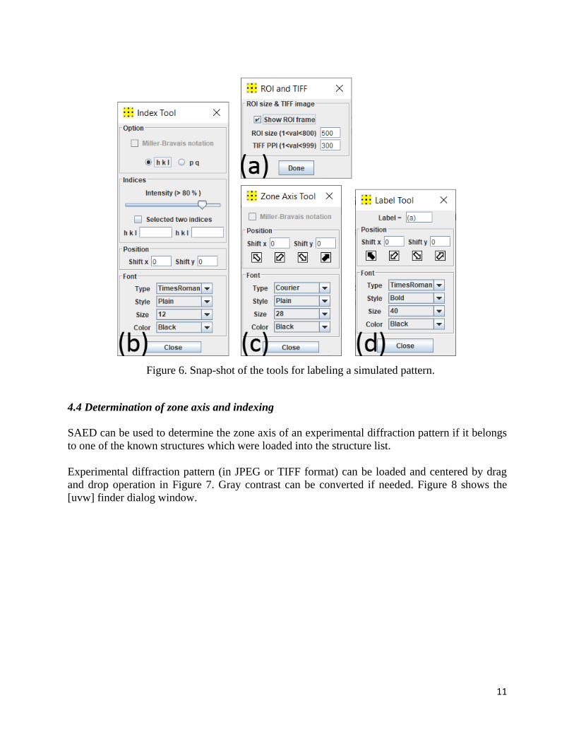
4.4 Determination of zone axis and indexing
SAED can be used to determine the zone axis of an experimental diffraction pattern if it belongs
to one of the known structures which were loaded into the structure list.
Experimental diffraction pattern (in JPEG or TIFF format) can be loaded and centered by drag
and drop operation in Figure 7. Gray contrast can be converted if needed. Figure 8 shows the
[uvw] finder dialog window.

12
Figure 7. Snap-shot of the tools for labeling a simulated pattern.
Step 1. Update the match factor. Use a Scale marker to calibrate the simulated pattern to match
with the experimental one (or a single diffraction spot/ring). The match factor can be saved, so it
does not need to be calibrated all time as soon as the same experimental conditions were used.
Step 2. Find the basic reciprocal vectors g1 and g2; the length can be labeled in (1/Å).
Step 3. Define the tolerance value (default as 5%) and find
the possible zone axis. The one with the least mismatching residue is shown, and the whole list
can be saved to a text file.
The tolerance value is defined as the maximum of percent errors: Ve = experimental value and
Vk = known value,
Percent error = (Ve - Vk)/ Vk x100%.
Step 4. The zone axis is obtained by matching the reciprocal length and angle between them. The
zone axis should be confirmed by comparing a simulated pattern to the experimental one.
Step 5. The list of all possible zone axes within the tolerance can be saved to an ASCII text file.
The zone axes, the measured g1 and g2 and angle, and their percent errors are listed in the file.
Figure 8. Snap-shot of the [uvw] finder.

13
5. Special topics on SAED
5.1 Partial occupancy factor and isotropic temperature facto
Some atom coordinates maybe not in full occupancy in a crystalline structure. In this case, the
occupancy factor (default value 1.0) should be changed to the values according to the crystalline
structure in preparation of the structure data file for electron diffraction simulation.
The partial occupancy factor can also be used to simulate a certain level of chemical order in
structure. For example, the chemical ordered FePt L10 phase, see section 6. In this case, a
different type of atoms may be assigned to the same atomic coordinates with a different
occupancy according to the chemical ratio, but the sum of the occupancy factors of the two
atoms is 1.0.
Isotropic temperature factor is used here to simulate the effect of lattice vibration (Debye model).
Although the isotropic temperature factor is a rough model, it can be used to simulate the
decrease of the diffraction intensity with the variation of the |g| value. The higher the value of |g|,
the more decrease of the diffraction intensity.
5.2 Load and center EDP
Experimental electron diffraction patterns can be loaded up and centered for analysis and
compare with simulated patterns. The experimental pattern in jpeg (.jpg) and tiff (.tif) formats
can be loaded using the window file system or the drag-and-drop box in the graphic menu bar.
The experimental pattern can be processed, e.g., invert, resize and rotate, and then center by
using Center in the Experiment menu. Once the Center is clicked, five concentric circles will
appear in the main panel. The pattern can be adjusted into the center of the panel by selecting
the center of the pattern while holding the left button of the mouse; Click the Center in the
Experiment menu, the pattern is locked up in the position, and concentric circles disappear.
More adjustments in small steps may be needed to find the accurate position. The number of
concentric circles can be changed using the Number of Reference Circle in the Option menu.
5.3 Determination of weight ratio of a multiple-phase system
The SAED program provides a way to roughly estimate the weight ratio of a composite
diffraction pattern of multiple phases. Adjust the mass proportion mp(i) of each phase to match
the relative intensities of its diffraction pattern to experimental patterns, then the final mass ratio
of phase i is,
𝑚𝑝(𝑖)
∑ 𝑚𝑝(𝑖)𝑖
5.4 Simulation of twins and coexisted multiple phases
Electron diffraction patterns of twins can be simulated using SAED. In order to generate twining
diffraction patterns, the same structure data is needed to be loaded multiple times according to
the number of twin components. In reciprocal space, the twin patterns may be generated by

14
rotation, mirror, or inverse operations. For the rotation twin, the twinning component can be
rotated in the calculation control panel. For reflection twin, the twining component can be
reflected at the horizontal mirror and then rotated to the requested angle. For inversion twin, the
twin component can be calculated using zone axes of [uvw] and [-u,-v,-w].
6. Examples
6.1 Pt-Bi thin film
There has been considerable interest in understanding various properties of Pt-Bi based
compounds because of their high activity as fuel-cell anode catalysts for formic acid (HCOOH)
or methanol (CH3OH) oxidation. Although Pt is regarded as one of the most efficient catalyst
materials, the main problem with this conventional catalyst is that it is readily poisoned by
carbon monoxide (CO) that is produced as a side product of the reaction. CO poisoning reduces
the catalytic activity and cell efficiency because it remains firmly bound to the electrode surface.
However, some recent reports show that the use of ordered intermetallic compound such as PtBi
as an electrode material exhibits an improved cell efficiency with a dramatic reduction in the CO
adsorption.
The three common intermetallic compounds based on Pt and Bi are PtBi, PtBi2 and Pt2Bi3.
Equiatomic PtBi phase is at the low temperature side of the phase diagram and may be off-
stoichiometric towards Pt-rich side. PtBi2 has four polymorphs namely α-PtBi2(oP24), β-
PtBi2(cP12), γ-PtBi2(hP9) and δ-PtBi2 (oP6) from low to high temperature in equilibrium phase
diagram. PtBi and Pt2Bi3 adopt the hexagonal NiAs structure (PtBi: a = 4.3240 and c = 5.501 Å;
Pt2Bi3: a = 4.13 and c = 5.58 Å) whereas the three polymorphs of PtBi2 crystallize in the AuSn2
type Orthorhombic (α-PtBi2: a = 6.732, b = 6.794 and c = 13.346 Å), FeS2 cubic pyrite (β-PtBi2:
a = 6.701 Å), and trigonal (γ-PtBi2: a = 6.57, and c = 6.16 Å) crystal structures, respectively.
Figure 9. SAED pattern of Pt-Bi thin film, which consists of the twin of -PtBi2 and coexisted
hexagonal PtBi phase, (a) experimental electron diffraction pattern (EDP), (b) simulated EDP,
and (c) simulated EDP with a single phase of -PtBi2.
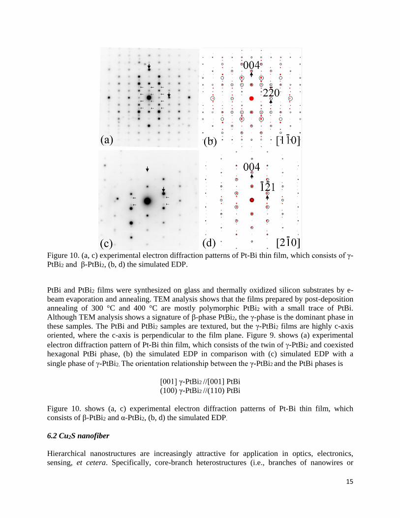
15
Figure 10. (a, c) experimental electron diffraction patterns of Pt-Bi thin film, which consists of γ-
PtBi2 and β-PtBi2, (b, d) the simulated EDP.
PtBi and PtBi2 films were synthesized on glass and thermally oxidized silicon substrates by e-
beam evaporation and annealing. TEM analysis shows that the films prepared by post-deposition
annealing of 300 °C and 400 °C are mostly polymorphic PtBi2 with a small trace of PtBi.
Although TEM analysis shows a signature of β-phase PtBi2, the γ-phase is the dominant phase in
these samples. The PtBi and PtBi2 samples are textured, but the γ-PtBi2 films are highly c-axis
oriented, where the c-axis is perpendicular to the film plane. Figure 9. shows (a) experimental
electron diffraction pattern of Pt-Bi thin film, which consists of the twin of -PtBi2 and coexisted
hexagonal PtBi phase, (b) the simulated EDP in comparison with (c) simulated EDP with a
single phase of -PtBi2. The orientation relationship between the γ-PtBi2 and the PtBi phases is
[001] γ-PtBi2 //[001] PtBi
(100) γ-PtBi2 //(110) PtBi
Figure 10. shows (a, c) experimental electron diffraction patterns of Pt-Bi thin film, which
consists of β-PtBi2 and α-PtBi2, (b, d) the simulated EDP.
6.2 Cu2S nanofiber
Hierarchical nanostructures are increasingly attractive for application in optics, electronics,
sensing, et cetera. Specifically, core-branch heterostructures (i.e., branches of nanowires or

16
nanorod on a central nanowire or nanofiber core), having core and branches composed of
different materials, allow targeted properties of the nanowires and the base, offer high surface-to-
volume ratio and nanowire-to-base ratio, and bring the promise of novel functional membranes.
A novel hierarchical architecture in our recent work, inorganic Cu2S nanowires standing on
organic polyacrylonitrile (PAN) nanofiber, has been produced by combining the electrospinning
technique and room-temperature gas-solid diffusion-assisted chemical growth.
The produced nanowires are 1.5~1.8 µm long with a uniform diameter of about 80 nm (Figure
11a). The single nanowires’ experimental EDPs match the monoclinic Cu2S crystal phase. They
indicate that the nanowires’ growth direction is perpendicular to the (2,0,-4) crystal plane, i.e.,
parallel to the monocrystal c axis (Figure 11b, 11c). The nanowires’ growth seems to precede the
formation of Cu2S sheath on the nanofibers’ surface.
Figure. 11. TEM images of the hierarchical structure (a). Experimental EDPs of the Cu2S
nanowires (b), arrows show the nanowire growth direction and corresponding simulated patterns
of monoclinic Cu2S crystal structure (c).
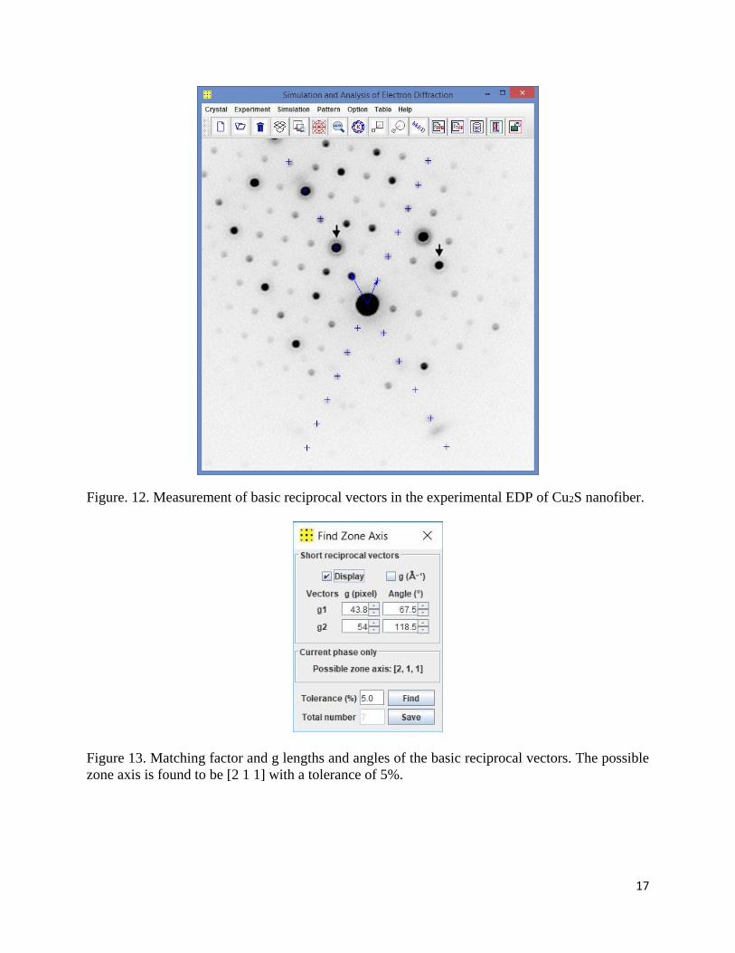
The basic reciprocal vectors for the experimental EDP are measured, as shown in Figure 12. The
calibrated matching factor and basic reciprocal vectors for the experimental EDP are listed in
Figure 13. The tolerance is chosen as 5%. The possible zone axis is found to be [2 1 1], and there
are seven possible zone axes, which can be saved to a file. Figure 14 shows the simulated
pattern of [2 1 1] zone axis matches well with the experimental EDP; thus, the zone axis and
index of the EDP are determined.
17
Figure. 12. Measurement of basic reciprocal vectors in the experimental EDP of Cu2S nanofiber.
Figure 13. Matching factor and g lengths and angles of the basic reciprocal vectors. The possible
zone axis is found to be [2 1 1] with a tolerance of 5%.

18
Figure. 14. Simulated EDP of Cu2S with zone axis [2 1 1].
7. Related programs: PAPM, SVAT, SAKI, SPICA, and PCED
All programs in the Landyne suite are using the input structure data in the same format. A few of
them are listed here, which can be used in combination with SAED. Users may check the
program specification or user manual for each program in detail.
7.1 ESPOT
ESPOT is an extension of SAED for generating an electrostatic potential (difference) map of a
crystal structure. SAED provides the calculated diffraction data for ESPOT. The experimental
diffraction data for ESPOT can be generated using QSAED.
7.2 SVAT
The need for a structure visualization/an analytical tool, using the same input data format in the
Landyne suite, becomes obvious with the growth of the programs and users.
7.3 SAKI

19
SAKI can be viewed as an extension of the SAED. SAKI can be used to simulate the Kikuchi
pattern and double diffraction effect; SAKI4 can also be used to determine the precise orientation
of a crystal using three pairs of Kikuchi lines.
7.4 SPICA
SPICA3 is the next version of early JECP/SP, which was designed for stereographic projection
with an application for specimen orientation adjustment using TEM holders. SPICA3 inherits
JECP/SP functions and extends to many new functions for crystallographic analysis with a more
user-friendly GUI design.
7.5 PCED
PCED4 is an upgraded version of the previous JECP/PCED. New features include (i)
Blackman’s theory, an integral two-beam dynamical theory, for intensity calculation, (ii) Match
model for out-of-plane and in-plane texture, (iii) pseudo-Voigt function for peak profile of
diffraction ring, and (iv) improvement on diffraction pattern indexing and matching to an
experimental pattern.
Reference:
Humphreys, C.J., The scattering of fast electrons by crystals, Rep.Prog.Phys., 42 (1970) 122.
Li, X.Z., PCED2.0 - A computer program for advanced simulation of polycrystalline electron
diffraction pattern. Ultramicroscopy 110 (2010) 297-304.
Li, X.Z., SAED3: simulation and analysis of electron diffraction patterns. Microscopy and
Analysis, May issue (2019) 16-19.
Li, X.Z. SVAT4: a computer program for visualization and analysis of crystal structures. Journal
of Applied Crystallography 53 (2020) 848-853.
Metherell, A.J.F., Diffraction of electrons by perfect crystals, Microscopy in Materials Science,
1975.
Peng, L.M., Dudarev, S.L., and Whelan, M.J., High Energy Electron Diffraction and Microscopy,
Oxford University Press, 2004.
Peng, L.M., Ren, G., Dudarev, S.L., and Whelan, M.J., Robust Parameterization of Elastic and
Absorptive Electron Atomic Scattering Factors, Acta Cryst. A52 (1996) 257.
Self, P.G., Practical computation of amplitudes and phases in electron
diffraction, Ultramicroscopy 11 (1983) 35.


