Using FlexIO for parallel Camera Interface, Application Note, Rev. 0, 04/2016
NXP Semiconductors 5
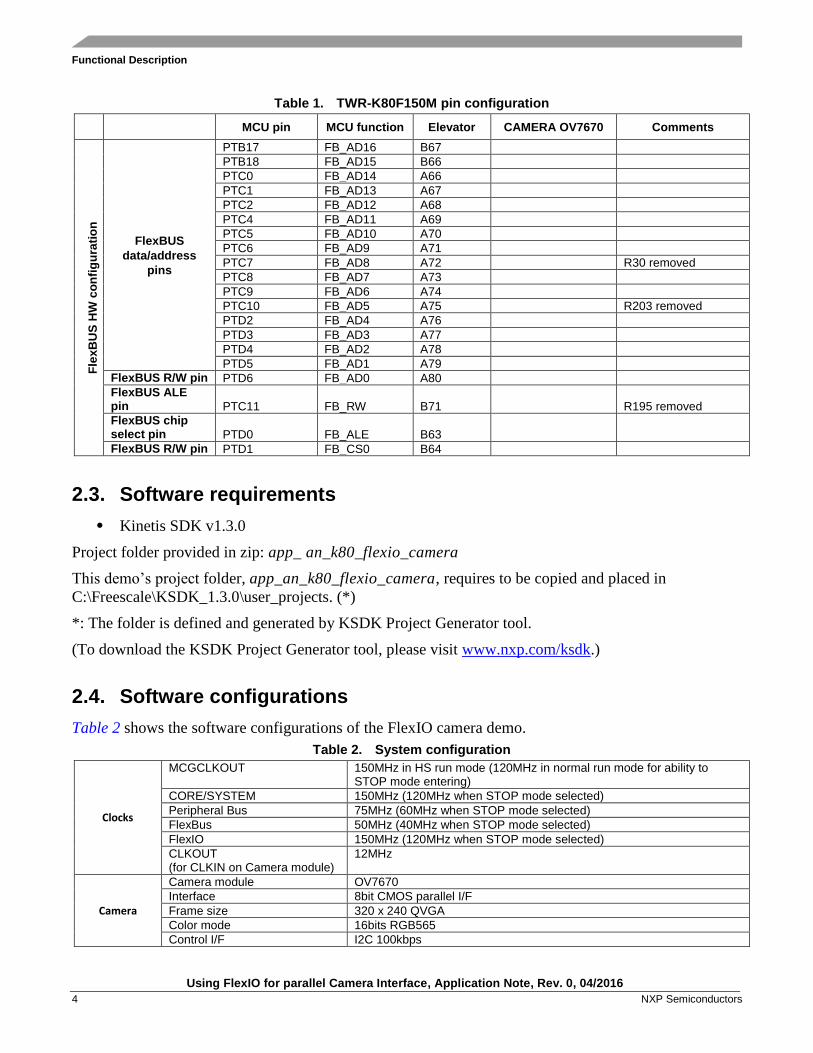
Table 2. System configuration
VSYNC 33 ms (30 fps)
FlexIO
Mode Parallel receive mode
Timer 1 timer
Shifter 8 shifters concatenated
Number of used pins 10 pins (8 data + 1 HREF + 1 PCLK)
eDMA
Ch 16 (not used in stop mode) Transfer from SRAM camera buffer to FlexBus(LCD 16bit width). 2 Byte transfer Minor loop = 16 Major loop = 4800 2byte x 16 x 4800 = 150kB
Ch 17 Transfer from FlexIO shift buffers to SRAM camera buffer. Minor loop = 32Byte burst transfer Major loop = 4800 32Byte x 4800 = 150kB
Ch 2 Restore initial address of LCD at VSYNC edge.
Ch 3 To restore eDMA ch17 iteration count (CITER) to synchronize with frame at VSYNC edge.
2.5. System workflow
Shifter 7
Shifter 6
Shifter 5
Shifter 4
Shifter 3
Shifter 2
Shifter 1
Shifter 0
Expiration
(32x)Timer 0
Shifter buffer 7
Shifter buffer 6
Shifter buffer 5
Shifter buffer 4
Shifter buffer 3
Shifter buffer 2
Shifter buffer 1
Shifter buffer 0
Store event
data sampling data shifting
Shifter status 0 set
150k QVGA frame buffer
32B burst
DMA
CH1
S D
DMA
CH0
SD
Tr
Tr
input trigger
output
FXIO_D24
FXIO_D25
FXIO_D26
FXIO_D27
FXIO_D28
FXIO_D29
FXIO_D30
FXIO_D31
PCLK
FXIO_D18HREF
D0
D7
D1
D2
Shift timing
D3
D4
D5
D6
SRAM_LeDMA
FXIO_D1
FlexBUS16 x 16-bits
per request
16-bit width (RGB565)
FB_AD0:15
FB_CS, FB_ALE
FB_RW K80F150M
VSYNC PORT, GPIOFalling edge
IRQ (or DMA)
Reset Source
address and
CITER
XCLK
I2CSDA
SIOD
OSC
SIOC
SCL
OSCERCLK
PTA13
Re
se
t LC
D w
ind
ow
FlexIO
Figure 2. System workflow
Functional Description
Using FlexIO for parallel Camera Interface, Application Note, Rev. 0, 04/2016
6 NXP Semiconductors
... ... ... ...
………
VSYNC
HREF
PCLK
D0
D1
D2
D7
.
.
.
... ...... ...
... ...... ...
... ...... ...
... ...... ...
………
………
………
………
………
1 frame
1 line
1. row 2. row n. row(n-1). row
n = 240 for QVGA
t
t
t
t
t
t
t
m pixels
(2 x m bytes for RGB565) m = 320 for QVGA
Figure 3. CMOS camera signal waveform
Figure 3 shows the system workflow and signal wave form of the FlexIO camera demo. The window
size and position for LCD display is configured with FlexBus at VSYNC edge. To make sure that a
frame is synchronized, eDMA Ch2 and Ch3 channels restore a loop counter of iteration count (CITER)
and DMA source and destination address for camera buffer to initial address at VSYNC edge. This
restoring source and destination address for buffer is necessary just in case that asynchronous interrupt
occurs.
FlexIO is configured as a receiving mode and parallel shift mode for 8-bit CMOS sensor camera I/F.
Arrays of 32-bit shifters in FlexIO are concatenated one after the other for buffering samples of captured
image. It can configure up to 32-byte buffer for receiving. Figure 4 shows the details of shift register
configuration. During HREF signal high, FlexIO shifters shift data in on pixel clock edge. DMA request
generates when 32-byte pixel data buffered in shifters has been loaded into shift buffers (SHIFTBUF
register is full). eDMA transfers the pixel data from SHIFTBUF into a camera frame buffer in SRAM.
The other channel of eDMA transfers the data in the camera buffer to LCD controller using FlexBus
interface to display on TFT LCD.
2.6. FlexIO configurations
2.6.1. FlexIO pin configuration
Table 1 shows the FlexIO data pins used in this demo. GPIO pins are multifunctional and multiplexed.
The pins need to be configured where external pins are used as FlexIO.
Kinetis SDK provides API programing interface to configure signal multiplexing. Also, clock gate to
those PORT pins and FlexIO module need to be enabled and called in hardware_init() function.
//hardware_init.c
/* enable clock for PORTs */
CLOCK_SYS_EnablePortClock(PORTA_IDX); //used as FlexIO
Functional Description
Using FlexIO for parallel Camera Interface, Application Note, Rev. 0, 04/2016
NXP Semiconductors 7
CLOCK_SYS_EnablePortClock(PORTB_IDX); //used as FlexIO
CLOCK_SYS_EnablePortClock(PORTC_IDX);
CLOCK_SYS_EnablePortClock(PORTD_IDX); //used as FlexIO
Using FlexIO for parallel Camera Interface, Application Note, Rev. 0, 04/2016
8 NXP Semiconductors
FlexIO has a capability to output and input data in serial or parallel. When the parallel receive mode is
configured, only Shifter 3 and 7 can support parallel capturing from FlexIO pins. Figure 3 shows the
FlexIO shifter configuration. FlexIO has 8 shifters with 32-bit length. The Shifter can be concatenated
each other to buffer a large size of data up to 32 byte. The shifter status flag (SHIFTSTAT[SSF]) is set
when the shift buffer (SHIFTBUFn) has been loaded with data from Shifter according to Shifter Mode
(SHIFTCTL[SMOD]). SSF can generate DMA request. In this demo, only the last shifter status flag
(Shifter 0) initiates DMA transfer. FlexIO Timer is configured as 16-bit timer with FXIO_D1 as clock
input, and it is enabled on rising edge on HREF (FXIO_D18) and disabled on falling edge on HREF.
The timer decrements on both edges of the pixel clock.
This example uses 8 chained Shifters for buffering (32 byte = 32bits x 8) to capture 16 pixels of image
data (RGB565: 2byte per one pixel), so that 32 shifts are required to shift in to the full of the shifters.
The timer compare value (TIMCMP0[15:0]) is then set to (the number of bits) x 2 -1 = 32 x 2 -1 = 63. When the timer value reaches zero, the pixel data in the shifter is loaded in SHIFTBUF and the SSF
flag is set.
2.6.2.1. Initializing FlexIO module
Kinetis SDK provides API programming interface to initialize FlexIO module and set user configuration
as an application need. To initialize FlexIO module, FLEXIO_DRV_Init() function is called and the user