Using IBIS Models for Timing AnalysisC6000 Hardware Applications
ABSTRACT
Today’s high-speed interfaces require strict timings and accurate system design. To achievethe necessary timings for a given system, input/output buffer information specification (IBIS)models must be used. These models accurately represent the device drivers under variousprocess conditions. Board characteristics, such as impedance, loading, length, number ofnodes, etc., affect how the device driver behaves. This application report discusses how toproperly use IBIS models to attain accurate timing analysis for a given system. This reportfocuses on the use of SDRAM with a TMS320C6000 DSP, but is applicable to all interfacesthat have setup and hold parameters.
1 IntroductionDigital signal processors (DSPs) and memories are tested to specifications given by theirrespective data sheets. These tests are performed under specific operating conditions given bythe data sheets. Any variation from these specific operating conditions will cause a change inbehavior from which the device was tested. These operating conditions include temperature,voltage, frequency, capacitive loading, impedance, etc.
Input/output buffer information specification (IBIS) is a fast and accurate way of modeling abuffer’s behavior over all process conditions. IBIS models are generated based on V/I curvesderived from full-circuit simulations and/or bench-top testing. In order to use IBIS models, asimulation package, from companies such as Hyperlynx or Mentor Graphics, must bepurchased. These simulation packages give accurate information on signal integrity issues thatmay occur based on system, board, and component-level characteristics.
For example, a DSP tester has a given test load. If a board has more or less loading than that ofthe tester, the timings will be skewed from what was originally intended. This can hurt or help thesystem, depending on which way the timing is skewed, and what parameter is of concern.
SPRA839A
3 Using IBIS Models for Timing Analysis
Important to this application report is that of impedance and loading. It is assumed thatfrequency remains constant, the voltage remains well within the data sheet specification range,and the temperature remains at or near room condition (well within the specification limits,normally 0�C and 90�C).
Systems that use multiple sychronous dynamic random-access memory (SDRAM) chips to fillthe bus width will have to do IBIS simulations on each component. This must be done sincethere is no longer a point-to-point connection between the DSP and the SDRAM. The variationsin trace lengths create differences in timings between the multiple components. Users mustperform IBIS simulations to ensure signal integrity.
This application report discusses the various reference points for timings that are important toboth the DSP and the SDRAM. In section 3, an overview of the tester used to test the DSPand/or the SDRAM is given along with an explanation of the timing variation between the testerand a typical board. Reference voltages and noise margins impact the timings presented by boththe tester and a typical board. An understanding of why this occurs is briefly discussed insections 4 and 5. Section 6 of this application report encompasses the formulas used toestablish setup and hold times for both the DSP and the SDRAM, based on IBIS Simulations.Section 7 summarizes the AC timing analysis procedures.
2 Establishing a Reference Point
Data sheet timings are measured from the pins of the device connected to the test board with agiven tester load. On a real system board, these timings change as loading increases ordecreases from the loading on the tester board. Before going into further details (in section 3) onhow timings differ on a real system board versus the test board, this section discusses how toestablish a reference point. A reference point must be established when modeling a board thatvaries from the original test board model. As a matter of convenience, the reference point istaken from just inside the master device, the DSP. The reference point represents the time inwhich the DSP output buffer is enabled.
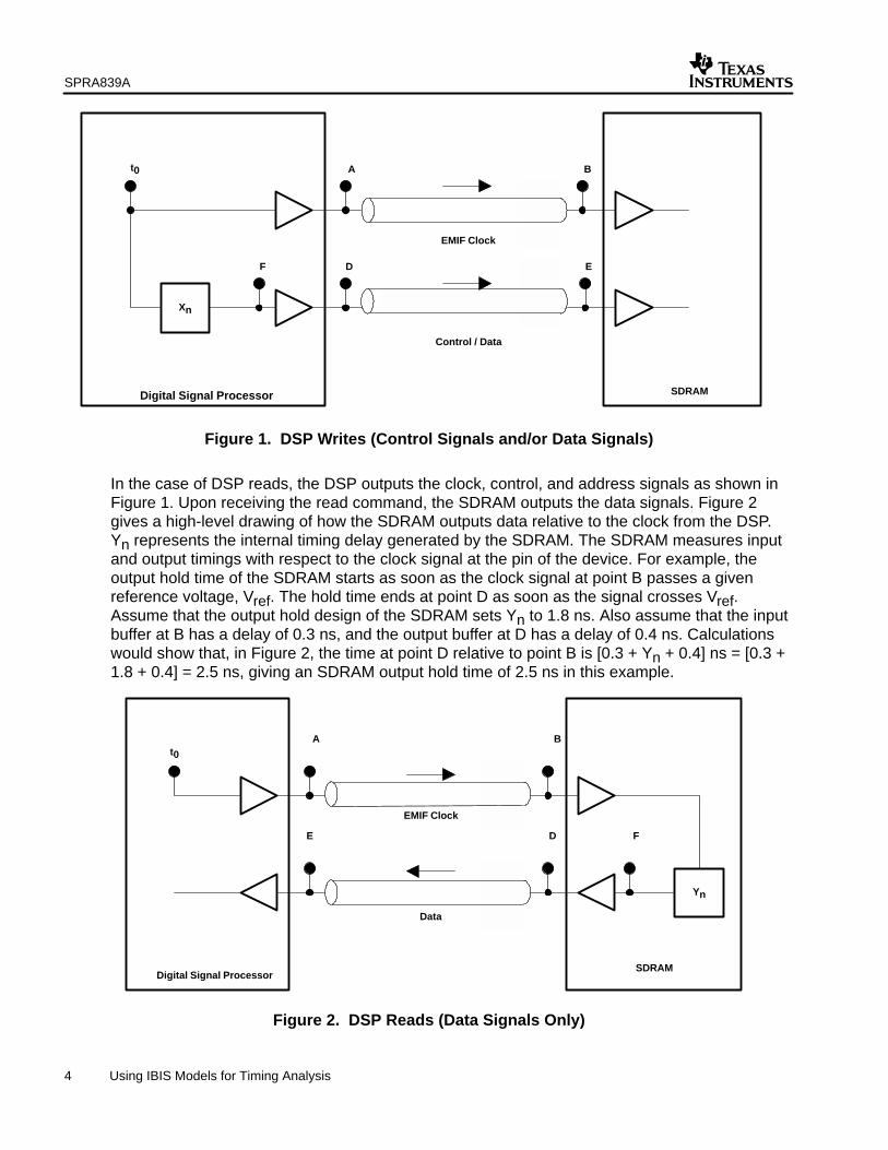
Figure 1 gives a high-level drawing of how a DSP write to SDRAM can be represented in a realsystem board. The point, denoted by t0, is the point in which all timings will be referenced. Thepoints A, B, D, and E are measured at the pins of the DSP and SDRAM, respectively. Point Fdescribes the point at which the output buffer turns on relative to time t0. Xn is an internal timingdelay that is represented by a constant value, fixed by the design of the DSP. Assume that thedesign of the DSP sets Xn to –3.1 ns. Also assume that the output buffer at A had an internaldelay of 0.2 ns, and the output buffer at D had an internal delay of 0.3 ns. Calculations wouldshow that the time at point A is (t0 + 0.2) ns, or simply 0.2 ns relative to t0, Similarly, calculationswould show that the time at point D is (t0 + Xn + 0.3) ns = (t0 – 3.1 + 0.3) ns, or simply –2.8 nsrelative to t0. The output setup time for the DSP is calculated from when the data transitions atpoint D, to when the clock transitions at point A. In this case, the output setup time is [0.2 –(–2.8)] ns = 3 ns.
Xn will be different for hold times, since this uses different internal logic to gate the buffers.
SPRA839A
4 Using IBIS Models for Timing Analysis
SDRAMDigital Signal Processor
BA
F D E
Control / Data
EMIF Clock
t0
Xn
Figure 1. DSP Writes (Control Signals and/or Data Signals)
In the case of DSP reads, the DSP outputs the clock, control, and address signals as shown inFigure 1. Upon receiving the read command, the SDRAM outputs the data signals. Figure 2gives a high-level drawing of how the SDRAM outputs data relative to the clock from the DSP.Yn represents the internal timing delay generated by the SDRAM. The SDRAM measures inputand output timings with respect to the clock signal at the pin of the device. For example, theoutput hold time of the SDRAM starts as soon as the clock signal at point B passes a givenreference voltage, Vref. The hold time ends at point D as soon as the signal crosses Vref.Assume that the output hold design of the SDRAM sets Yn to 1.8 ns. Also assume that the inputbuffer at B has a delay of 0.3 ns, and the output buffer at D has a delay of 0.4 ns. Calculationswould show that, in Figure 2, the time at point D relative to point B is [0.3 + Yn + 0.4] ns = [0.3 +1.8 + 0.4] = 2.5 ns, giving an SDRAM output hold time of 2.5 ns in this example.
SDRAMDigital Signal Processor
BA
FDE
Data
EMIF Clock
t0
Yn
Figure 2. DSP Reads (Data Signals Only)
SPRA839A
5 Using IBIS Models for Timing Analysis
Both the DSP and the SDRAM measure input and output timings with respect to the clock signalat the pin of the device. Output times are measured when Vref is crossed at the data/controlsignal relative to when Vref is crossed at the clock. Input times are measured when thedata/control signal goes valid (setup times) or invalid (hold times) relative to when Vref is crossedat the clock.
3 Understanding the Tester
3.1 Tester Load Adjustment
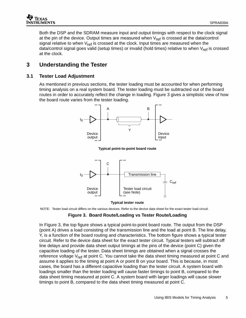
As mentioned in previous sections, the tester loading must be accounted for when performingtiming analysis on a real system board. The tester loading must be subtracted out of the boardroutes in order to accurately reflect the change in loading. Figure 3 gives a simplistic view of howthe board route varies from the tester loading.
Y
A
Deviceoutput
B
Deviceinput
outputDevice
(see Note)Tester load circuit
C
Transmission line
Cref
Typical point-to-point board route
Typical tester route
t0
t0
NOTE: Tester load circuit differs on the various devices. Refer to the device data sheet for the exact tester load circuit.
Figure 3. Board Route/Loading vs Tester Route/Loading
In Figure 3, the top figure shows a typical point-to-point board route. The output from the DSP(point A) drives a load consisting of the transmission line and the load at point B. The line delay,Y, is a function of the board routing and characteristics. The bottom figure shows a typical testercircuit. Refer to the device data sheet for the exact tester circuit. Typical testers will subtract offline delays and provide data sheet output timings at the pins of the device (point C) given thecapacitive loading of the tester. Data sheet timings are obtained when a signal crosses thereference voltage Vref at point C. You cannot take the data sheet timing measured at point C andassume it applies to the timing at point A or point B on your board. This is because, in mostcases, the board has a different capacitive loading than the tester circuit. A system board withloadings smaller than the tester loading will cause faster timings to point B, compared to thedata sheet timing measured at point C. A system board with larger loadings will cause slowertimings to point B, compared to the data sheet timing measured at point C.
SPRA839A
6 Using IBIS Models for Timing Analysis
By providing the proper board route characteristics (Y) and IBIS models for the DSP and theSDRAM, IBIS simulations can be used to measure the actual timings at point B and C,respectively. IBIS simulators have the ability to give absolute timings or reference timings.Absolute timings are measured from when the buffer is turned on at t0. Reference timings aremeasured from when the output pin under test reaches the reference voltage. For example,absolute timing at point B is measured from t0, while reference timing at point B is measuredfrom when the output at A reaches the reference voltage. For AC timing analysis, use absolutetimings in IBIS simulations to establish a common reference point for both the system boardcircuit and the tester circuit. Absolute timings are represented by a subscript 0. Performing IBISsimulations with the proper IBIS models and board route characteristics, you can obtain B0, theabsolute delay measured from t0 to B. Similarly, you can perform IBIS simulations to obtain C0,the absolute delay from t0 to C. The following equation gives the difference between the actualtiming seen at the pin of the SDRAM (B0) and the data sheet timing (C0):
Difference between timing at SDRAM and data sheet = B0 – C0
As shown in Figure 3, the board delay Y is represented by this equation:
Y = B0 – A0
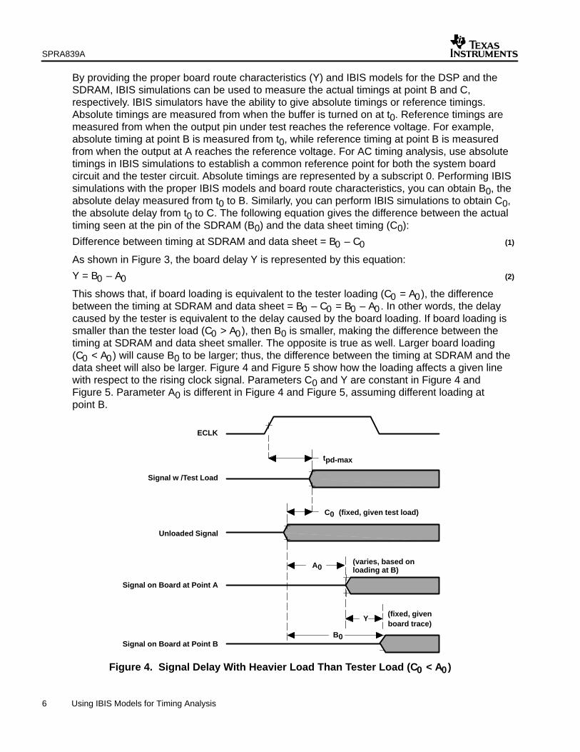
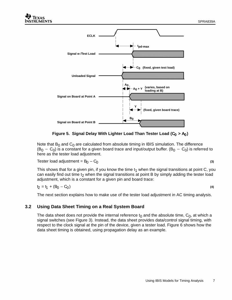
This shows that, if board loading is equivalent to the tester loading (C0 = A0 ), the differencebetween the timing at SDRAM and data sheet = B0 – C0 = B0 – A0 . In other words, the delaycaused by the tester is equivalent to the delay caused by the board loading. If board loading issmaller than the tester load (C0 > A0 ), then B0 is smaller, making the difference between thetiming at SDRAM and data sheet smaller. The opposite is true as well. Larger board loading (C0 < A0 ) will cause B0 to be larger; thus, the difference between the timing at SDRAM and thedata sheet will also be larger. Figure 4 and Figure 5 show how the loading affects a given linewith respect to the rising clock signal. Parameters C0 and Y are constant in Figure 4 andFigure 5. Parameter A0 is different in Figure 4 and Figure 5, assuming different loading atpoint B.
A0
C0
tpd-max
ECLK
Signal w /Test Load
Unloaded Signal
Signal on Board at Point A
Y
B0Signal on Board at Point B
(varies, based on loading at B)
(fixed, givenboard trace)
(fixed, given test load)
Figure 4. Signal Delay With Heavier Load Than Tester Load (C0 < A0 )
(1)
(2)
SPRA839A
7 Using IBIS Models for Timing Analysis
A0
C0
tpd-max
ECLK
Signal w /Test Load
Unloaded Signal
Signal on Board at Point A
Y
B0Signal on Board at Point B
A0 + Y
(fixed, given test load)
(varies, based on loading at B)
(fixed, given board trace)
Figure 5. Signal Delay With Lighter Load Than Tester Load (C0 > A0 )
Note that B0 and C0 are calculated from absolute timing in IBIS simulation. The difference (B0 � C0) is a constant for a given board trace and input/output buffer. (B0 � C0) is referred tohere as the tester load adjustment.
Tester load adjustment = B0 – C0
This shows that for a given pin, if you know the time t1 when the signal transitions at point C, youcan easily find out time t2 when the signal transitions at point B by simply adding the tester loadadjustment, which is a constant for a given pin and board trace:
t2 = t1 + (B0 – C0)
The next section explains how to make use of the tester load adjustment in AC timing analysis.
3.2 Using Data Sheet Timing on a Real System Board
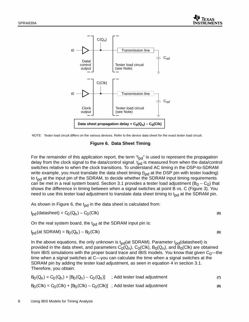
The data sheet does not provide the internal reference t0 and the absolute time, C0, at which asignal switches (see Figure 3). Instead, the data sheet provides data/control signal timing, withrespect to the clock signal at the pin of the device, given a tester load. Figure 6 shows how thedata sheet timing is obtained, using propagation delay as an example.
(3)
(4)
SPRA839A
8 Using IBIS Models for Timing Analysis
t0
(see Note)Tester load circuit
C(Clk)
Transmission line
Cref
t0 Transmission line
Tester load circuit
C(Qn)
(see Note)
CrefData/
controloutput
Clockoutput
Data sheet propagation delay = C0(Qn) – C0(Clk)
NOTE: Tester load circuit differs on the various devices. Refer to the device data sheet for the exact tester load circuit.
Figure 6. Data Sheet Timing
For the remainder of this application report, the term “tpd” is used to represent the propagationdelay from the clock signal to the data/control signal. tpd is measured from when the data/controlswitches relative to when the clock transitions. To understand AC timing in the DSP-to-SDRAMwrite example, you must translate the data sheet timing (tpd at the DSP pin with tester loading)to tpd at the input pin of the SDRAM, to decide whether the SDRAM input timing requirementscan be met in a real system board. Section 3.1 provides a tester load adjustment (B0 – C0) thatshows the difference in timing between when a signal switches at point B vs. C (Figure 3). Youneed to use this tester load adjustment to translate data sheet timing to tpd at the SDRAM pin.
As shown in Figure 6, the tpd in the data sheet is calculated from:
tpd(datasheet) = C0(Qn) – C0(Clk)
On the real system board, the tpd at the SDRAM input pin is:
tpd(at SDRAM) = B0(Qn) – B0(Clk)
In the above equations, the only unknown is tpd(at SDRAM). Parameter tpd(datasheet) isprovided in the data sheet, and parameters C0(Qn), C0(Clk), B0(Qn), and B0(Clk) are obtainedfrom IBIS simulations with the proper board trace and IBIS models. You know that given C0—thetime when a signal switches at C—you can calculate the time when a signal switches at theSDRAM pin by adding the tester load adjustment, as seen in equation 4 in section 3.1.Therefore, you obtain:
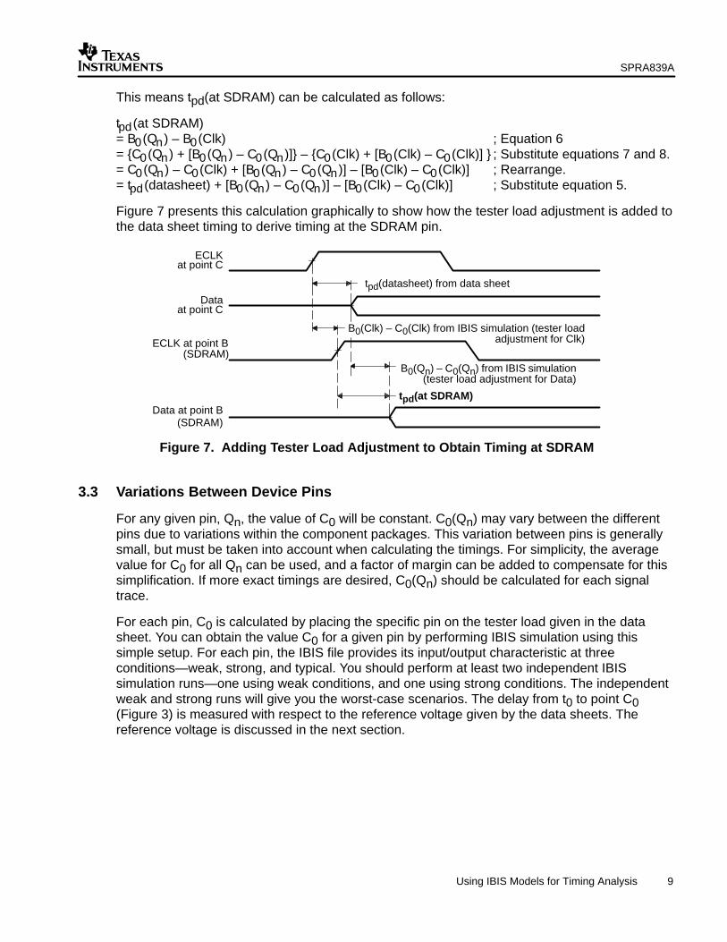
Figure 7 presents this calculation graphically to show how the tester load adjustment is added tothe data sheet timing to derive timing at the SDRAM pin.
ECLKat point C
Dataat point C
ECLK at point B(SDRAM)
Data at point B(SDRAM)
tpd(datasheet) from data sheet
B0(Clk) – C0(Clk) from IBIS simulation (tester loadadjustment for Clk)
B0(Qn) – C0(Qn) from IBIS simulation(tester load adjustment for Data)
tpd(at SDRAM)
Figure 7. Adding Tester Load Adjustment to Obtain Timing at SDRAM
3.3 Variations Between Device Pins
For any given pin, Qn, the value of C0 will be constant. C0(Qn) may vary between the differentpins due to variations within the component packages. This variation between pins is generallysmall, but must be taken into account when calculating the timings. For simplicity, the averagevalue for C0 for all Qn can be used, and a factor of margin can be added to compensate for thissimplification. If more exact timings are desired, C0(Qn) should be calculated for each signaltrace.
For each pin, C0 is calculated by placing the specific pin on the tester load given in the datasheet. You can obtain the value C0 for a given pin by performing IBIS simulation using thissimple setup. For each pin, the IBIS file provides its input/output characteristic at threeconditions—weak, strong, and typical. You should perform at least two independent IBISsimulation runs—one using weak conditions, and one using strong conditions. The independentweak and strong runs will give you the worst-case scenarios. The delay from t0 to point C0(Figure 3) is measured with respect to the reference voltage given by the data sheets. Thereference voltage is discussed in the next section.
SPRA839A
10 Using IBIS Models for Timing Analysis
4 The Reference Voltage
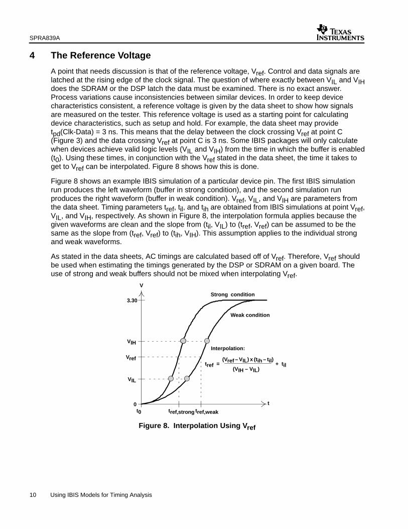
A point that needs discussion is that of the reference voltage, Vref. Control and data signals arelatched at the rising edge of the clock signal. The question of where exactly between VIL and VIHdoes the SDRAM or the DSP latch the data must be examined. There is no exact answer.Process variations cause inconsistencies between similar devices. In order to keep devicecharacteristics consistent, a reference voltage is given by the data sheet to show how signalsare measured on the tester. This reference voltage is used as a starting point for calculatingdevice characteristics, such as setup and hold. For example, the data sheet may providetpd(Clk-Data) = 3 ns. This means that the delay between the clock crossing Vref at point C(Figure 3) and the data crossing Vref at point C is 3 ns. Some IBIS packages will only calculatewhen devices achieve valid logic levels (VIL and VIH) from the time in which the buffer is enabled(t0). Using these times, in conjunction with the Vref stated in the data sheet, the time it takes toget to Vref can be interpolated. Figure 8 shows how this is done.
Figure 8 shows an example IBIS simulation of a particular device pin. The first IBIS simulationrun produces the left waveform (buffer in strong condition), and the second simulation runproduces the right waveform (buffer in weak condition). Vref, VIL, and VIH are parameters fromthe data sheet. Timing parameters tref, til, and tih are obtained from IBIS simulations at point Vref,VIL, and VIH, respectively. As shown in Figure 8, the interpolation formula applies because thegiven waveforms are clean and the slope from (til, VIL) to (tref, Vref) can be assumed to be thesame as the slope from (tref, Vref) to (tih, VIH). This assumption applies to the individual strongand weak waveforms.
As stated in the data sheets, AC timings are calculated based off of Vref. Therefore, Vref shouldbe used when estimating the timings generated by the DSP or SDRAM on a given board. Theuse of strong and weak buffers should not be mixed when interpolating Vref.
3.30
VIH
VIL
V
t
Vref
Interpolation:
0t0
tref =(Vref – VIL) x (tih – til) + til
(VIH – VIL)
tref,strong tref,weak
Strong condition
Weak condition
Figure 8. Interpolation Using Vref
SPRA839A
11 Using IBIS Models for Timing Analysis
4.1 Understanding Vref Measured on Tester vs. Real Board
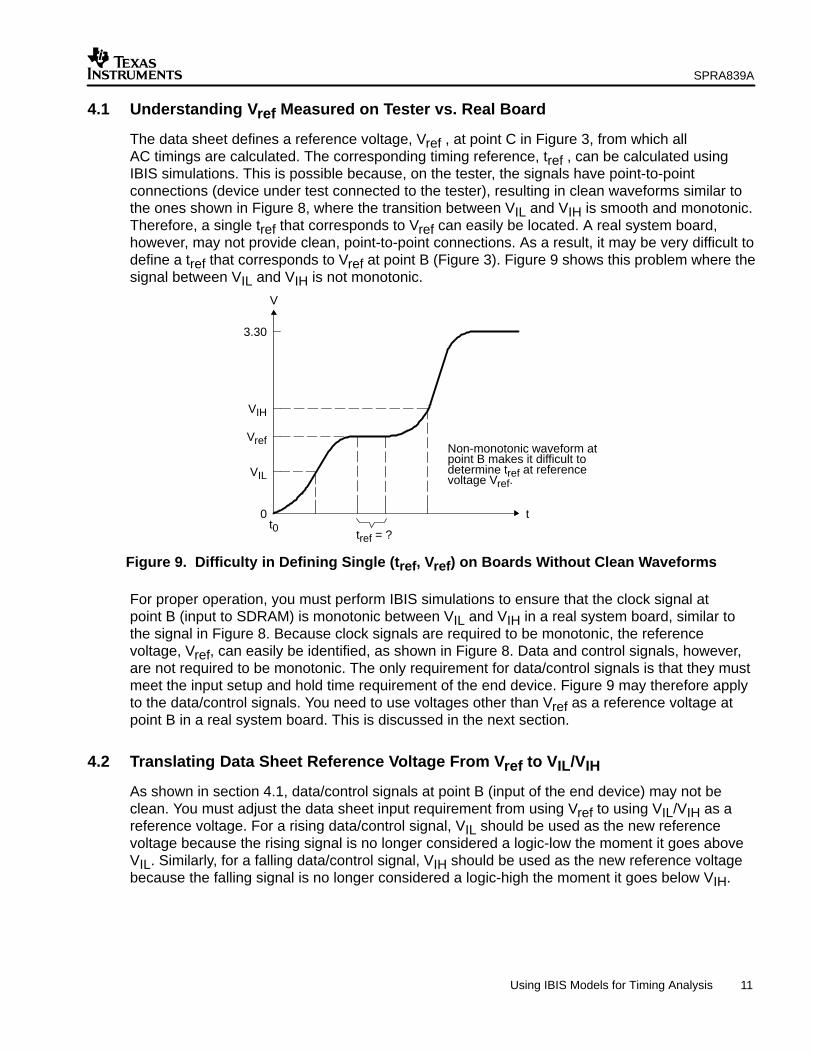
The data sheet defines a reference voltage, Vref , at point C in Figure 3, from which allAC timings are calculated. The corresponding timing reference, tref , can be calculated usingIBIS simulations. This is possible because, on the tester, the signals have point-to-pointconnections (device under test connected to the tester), resulting in clean waveforms similar tothe ones shown in Figure 8, where the transition between VIL and VIH is smooth and monotonic.Therefore, a single tref that corresponds to Vref can easily be located. A real system board,however, may not provide clean, point-to-point connections. As a result, it may be very difficult todefine a tref that corresponds to Vref at point B (Figure 3). Figure 9 shows this problem where thesignal between VIL and VIH is not monotonic.
3.30
VIH
Vref
VIL
0t0
t
V
Non-monotonic waveform atpoint B makes it difficult todetermine tref at referencevoltage Vref.
tref = ?
Figure 9. Difficulty in Defining Single (tref, Vref) on Boards Without Clean Waveforms
For proper operation, you must perform IBIS simulations to ensure that the clock signal atpoint B (input to SDRAM) is monotonic between VIL and VIH in a real system board, similar tothe signal in Figure 8. Because clock signals are required to be monotonic, the referencevoltage, Vref, can easily be identified, as shown in Figure 8. Data and control signals, however,are not required to be monotonic. The only requirement for data/control signals is that they mustmeet the input setup and hold time requirement of the end device. Figure 9 may therefore applyto the data/control signals. You need to use voltages other than Vref as a reference voltage atpoint B in a real system board. This is discussed in the next section.
4.2 Translating Data Sheet Reference Voltage From Vref to VIL/VIH
As shown in section 4.1, data/control signals at point B (input of the end device) may not beclean. You must adjust the data sheet input requirement from using Vref to using VIL/VIH as areference voltage. For a rising data/control signal, VIL should be used as the new referencevoltage because the rising signal is no longer considered a logic-low the moment it goes aboveVIL. Similarly, for a falling data/control signal, VIH should be used as the new reference voltagebecause the falling signal is no longer considered a logic-high the moment it goes below VIH.
SPRA839A
12 Using IBIS Models for Timing Analysis
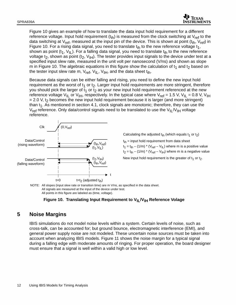
Figure 10 gives an example of how to translate the data input hold requirement for a differentreference voltage. Input hold requirement (tih) is measured from the clock switching at Vref to thedata switching at Vref, measured at the input pin of the device. This is shown at point (tih, Vref) inFigure 10. For a rising data signal, you need to translate tih to the new reference voltage t1,shown as point (t1, VIL). For a falling data signal, you need to translate tih to the new referencevoltage t2, shown as point (t2, VIH). The tester provides input signals to the device under test at aspecified input slew rate, measured in the unit volt per nanosecond (V/ns) and shown as slopem in Figure 10. The algebraic equations in this figure show the calculation of t1 and t2 based onthe tester input slew rate m, Vref, VIL, VIH, and the data sheet tih.
Because data signals can be either falling and rising, you need to define the new input holdrequirement as the worst of t1 or t2. Larger input hold requirements are more stringent, thereforeyou should pick the larger of t1 or t2 as your new input hold requirement referenced at the newreference voltage VIL or VIH, respectively. In the typical case where Vref = 1.5 V, VIL = 0.8 V, VIH= 2.0 V, t2 becomes the new input hold requirement because it is larger (and more stringent)than t1. As mentioned in section 4.1, clock signals are monotonic; therefore, they can use theVref reference. Only data/control signals need to be translated to use the VIL/VIH voltagereference.
Calculating the adjusted tih (which equals t1 or t2)
t1 = tih – (1/m) * (Vref – VIL) where m is a positive value
t2 = tih – (1/m) * (Vref – VIH) where m is a negative value
t
(0,Vref)
(tih,Vref)(t1,VIL)
(t2,VIH)(tih,Vref)
t=0 t=t2 (adjusted tih)
Clk
Data/Control(rising waveform)
Data/Control(falling waveform)
New input hold requirement is the greater of t1 or t2.
tih = input hold requirement from data sheet
NOTE: All slopes (input slew rate or transition time) are m V/ns, as specified in the data sheet.All signals are measured at the input of the device under test.All points in this figure are labeled as (time, voltage).
Figure 10. Translating Input Requirement to VIL/VIH Reference Volage
5 Noise Margins
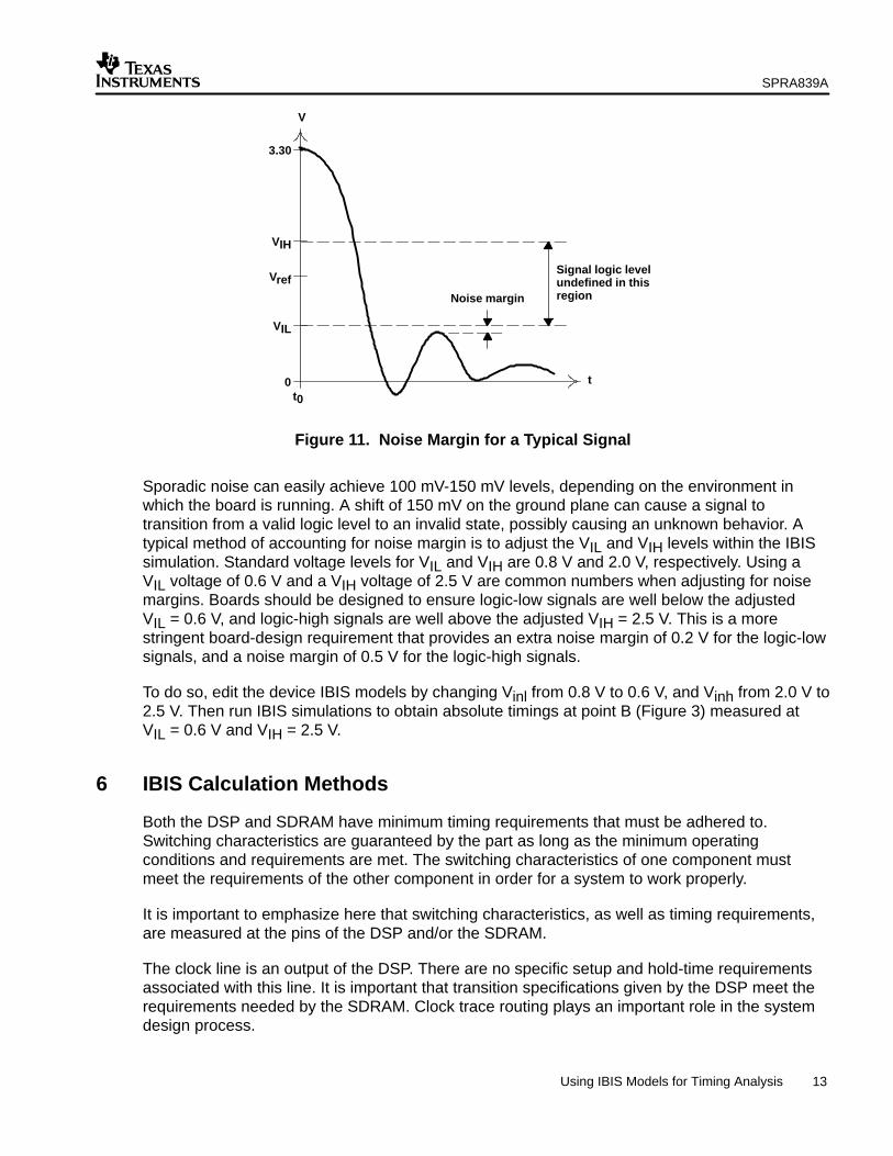
IBIS simulations do not model noise levels within a system. Certain levels of noise, such ascross-talk, can be accounted for; but ground bounce, electromagnetic interference (EMI), andgeneral power supply noise are not modeled. These uncertain noise sources must be taken intoaccount when analyzing IBIS models. Figure 11 shows the noise margin for a typical signalduring a falling edge with moderate amounts of ringing. For proper operation, the board designermust ensure that a signal is well within a valid high or low level.
SPRA839A
13 Using IBIS Models for Timing Analysis
3.30
VIH
VIL
V
t
Vref
0t0
Noise margin
Signal logic levelundefined in thisregion
Figure 11. Noise Margin for a Typical Signal
Sporadic noise can easily achieve 100 mV-150 mV levels, depending on the environment inwhich the board is running. A shift of 150 mV on the ground plane can cause a signal totransition from a valid logic level to an invalid state, possibly causing an unknown behavior. Atypical method of accounting for noise margin is to adjust the VIL and VIH levels within the IBISsimulation. Standard voltage levels for VIL and VIH are 0.8 V and 2.0 V, respectively. Using a VIL voltage of 0.6 V and a VIH voltage of 2.5 V are common numbers when adjusting for noisemargins. Boards should be designed to ensure logic-low signals are well below the adjusted VIL = 0.6 V, and logic-high signals are well above the adjusted VIH = 2.5 V. This is a morestringent board-design requirement that provides an extra noise margin of 0.2 V for the logic-lowsignals, and a noise margin of 0.5 V for the logic-high signals.
To do so, edit the device IBIS models by changing Vinl from 0.8 V to 0.6 V, and Vinh from 2.0 V to2.5 V. Then run IBIS simulations to obtain absolute timings at point B (Figure 3) measured at VIL = 0.6 V and VIH = 2.5 V.
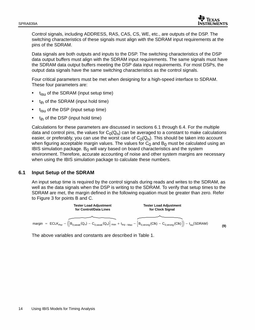
6 IBIS Calculation Methods
Both the DSP and SDRAM have minimum timing requirements that must be adhered to.Switching characteristics are guaranteed by the part as long as the minimum operatingconditions and requirements are met. The switching characteristics of one component mustmeet the requirements of the other component in order for a system to work properly.
It is important to emphasize here that switching characteristics, as well as timing requirements,are measured at the pins of the DSP and/or the SDRAM.
The clock line is an output of the DSP. There are no specific setup and hold-time requirementsassociated with this line. It is important that transition specifications given by the DSP meet therequirements needed by the SDRAM. Clock trace routing plays an important role in the systemdesign process.
SPRA839A
14 Using IBIS Models for Timing Analysis
Control signals, including ADDRESS, RAS, CAS, CS, WE, etc., are outputs of the DSP. Theswitching characteristics of these signals must align with the SDRAM input requirements at thepins of the SDRAM.
Data signals are both outputs and inputs to the DSP. The switching characteristics of the DSPdata output buffers must align with the SDRAM input requirements. The same signals must havethe SDRAM data output buffers meeting the DSP data input requirements. For most DSPs, theoutput data signals have the same switching characteristics as the control signals.
Four critical parameters must be met when designing for a high-speed interface to SDRAM.These four parameters are:
• tisu of the SDRAM (input setup time)
• tih of the SDRAM (input hold time)
• tisu of the DSP (input setup time)
• tih of the DSP (input hold time)
Calculations for these parameters are discussed in sections 6.1 through 6.4. For the multipledata and control pins, the values for C0(Qn) can be averaged to a constant to make calculationseasier, or preferably, you can use the worst case of C0(Qn). This should be taken into accountwhen figuring acceptable margin values. The values for C0 and B0 must be calculated using anIBIS simulation package. B0 will vary based on board characteristics and the systemenvironment. Therefore, accurate accounting of noise and other system margins are necessarywhen using the IBIS simulation package to calculate these numbers.
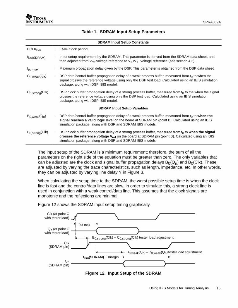
6.1 Input Setup of the SDRAM
An input setup time is required by the control signals during reads and writes to the SDRAM, aswell as the data signals when the DSP is writing to the SDRAM. To verify that setup times to theSDRAM are met, the margin defined in the following equation must be greater than zero. Referto Figure 3 for points B and C.
The above variables and constants are described in Table 1.
(9)
SPRA839A
15 Using IBIS Models for Timing Analysis
Table 1. SDRAM Input Setup Parameters
SDRAM Input Setup Constants
ECLKPer : EMIF clock period
tisu(SDRAM) : Input setup requirement by the SDRAM. This parameter is derived from the SDRAM data sheet, andthen adjusted from Vref voltage reference to VIL/VIH voltage reference (see section 4.2).
tpd-max : Maximum propagation delay given by the DSP. This parameter is obtained from the DSP data sheet.
C0,weak(Qn) : DSP data/control buffer propagation delay of a weak process buffer, measured from t0 to when thesignal crosses the reference voltage using only the DSP test load. Calculated using an IBIS simulationpackage, along with DSP IBIS model.
C0,strong(Clk) : DSP clock buffer propagation delay of a strong process buffer, measured from t0 to the when the signalcrosses the reference voltage using only the DSP test load. Calculated using an IBIS simulationpackage, along with DSP IBIS model.
SDRAM Input Setup Variables
B0,weak(Qn) : DSP data/control buffer propagation delay of a weak process buffer, measured from t0 to when thesignal reaches a valid logic level on the board at SDRAM pin (point B). Calculated using an IBISsimulation package, along with DSP and SDRAM IBIS models.
B0,strong(Clk) : DSP clock buffer propagation delay of a strong process buffer, measured from t0 to when the signalcrosses the reference voltage Vref on the board at SDRAM pin (point B). Calculated using an IBISsimulation package, along with DSP and SDRAM IBIS models.
The input setup of the SDRAM is a minimum requirement; therefore, the sum of all theparameters on the right side of the equation must be greater than zero. The only variables thatcan be adjusted are the clock and signal buffer propagation delays B0(Qn) and B0(Clk). Theseare adjusted by varying the trace characteristics, such as length, impedance, etc. In other words,they can be adjusted by varying line delay Y in Figure 3.
When calculating the setup time to the SDRAM, the worst possible setup time is when the clockline is fast and the control/data lines are slow. In order to simulate this, a strong clock line isused in conjunction with a weak control/data line. This assumes that the clock signals aremonotonic and the reflections are minimal.
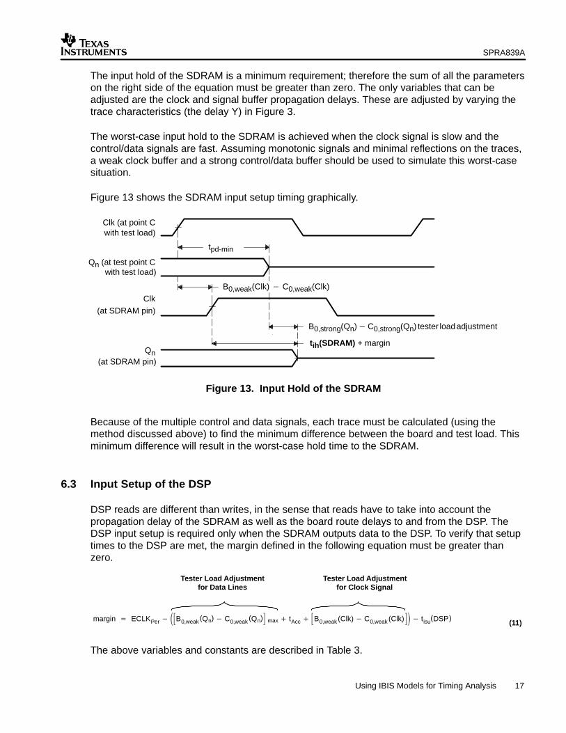
Figure 12 shows the SDRAM input setup timing graphically.
Because of the multiple control and data signals, each trace must be calculated (using themethod discussed above) to find the maximum difference between the board and test load. Thismaximum difference will result in the worst-case setup time to the SDRAM. Although all the datalines may use similar buffers within a given device, the package characteristics cause variationsin the output signal at the pins. When calculating the difference between the board propagationdelay and the test load propagation delay, it is important to use the same pin. Using separatepins to make this calculation will result in incorrect simulations.
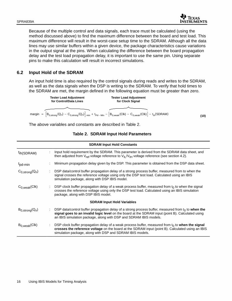
6.2 Input Hold of the SDRAM
An input hold time is also required by the control signals during reads and writes to the SDRAM,as well as the data signals when the DSP is writing to the SDRAM. To verify that hold times tothe SDRAM are met, the margin defined in the following equation must be greater than zero.
margin �
�B0,strong (Qn)� C0,strong (Qn)� min � tPd�Min �
�B0,weak (Clk) � C0,weak (Clk)� � tih(SDRAM)
Tester Load Adjustmentfor Control/Data Lines
Tester Load Adjustmentfor Clock Signal
The above variables and constants are described in Table 2.
Table 2. SDRAM Input Hold Parameters
SDRAM Input Hold Constants
tih(SDRAM) : Input hold requirement by the SDRAM. This parameter is derived from the SDRAM data sheet, andthen adjusted from Vref voltage reference to VIL/VIH voltage reference (see section 4.2).
tpd-min : Minimum propagation delay given by the DSP. This parameter is obtained from the DSP data sheet.
C0,strong(Qn) : DSP data/control buffer propagation delay of a strong process buffer, measured from to when thesignal crosses the reference voltage using only the DSP test load. Calculated using an IBISsimulation package, along with DSP IBIS model.
C0,weak(Clk) : DSP clock buffer propagation delay of a weak process buffer, measured from t0 to when the signalcrosses the reference voltage using only the DSP test load. Calculated using an IBIS simulationpackage, along with DSP IBIS model.
SDRAM Input Hold Variables
B0,strong(Qn) : DSP data/control buffer propagation delay of a strong process buffer, measured from t0 to when thesignal goes to an invalid logic level on the board at the SDRAM input (point B). Calculated usingan IBIS simulation package, along with DSP and SDRAM IBIS models.
B0,weak(Clk) : DSP clock buffer propagation delay of a weak process buffer, measured from t0 to when the signalcrosses the reference voltage on the board at the SDRAM input (point B). Calculated using an IBISsimulation package, along with DSP and SDRAM IBIS models.
(10)
SPRA839A
17 Using IBIS Models for Timing Analysis
The input hold of the SDRAM is a minimum requirement; therefore the sum of all the parameterson the right side of the equation must be greater than zero. The only variables that can beadjusted are the clock and signal buffer propagation delays. These are adjusted by varying thetrace characteristics (the delay Y) in Figure 3.
The worst-case input hold to the SDRAM is achieved when the clock signal is slow and thecontrol/data signals are fast. Assuming monotonic signals and minimal reflections on the traces,a weak clock buffer and a strong control/data buffer should be used to simulate this worst-casesituation.
Figure 13 shows the SDRAM input setup timing graphically.
Because of the multiple control and data signals, each trace must be calculated (using themethod discussed above) to find the minimum difference between the board and test load. Thisminimum difference will result in the worst-case hold time to the SDRAM.
6.3 Input Setup of the DSP
DSP reads are different than writes, in the sense that reads have to take into account thepropagation delay of the SDRAM as well as the board route delays to and from the DSP. TheDSP input setup is required only when the SDRAM outputs data to the DSP. To verify that setuptimes to the DSP are met, the margin defined in the following equation must be greater thanzero.
The above variables and constants are described in Table 3.
(11)
SPRA839A
18 Using IBIS Models for Timing Analysis
Table 3. DSP Input Setup Parameters
DSP Input Setup Constants
ECLKPer : EMIF clock period
tisu(DSP) : Input setup requirement by the DSP. This parameter is derived from the DSP data sheet, and thenadjusted from Vref voltage reference to VIL/VIH voltage reference (see section 4.2).
tAcc : Maximum access time given by the SDRAM. This parameter is obtained from the SDRAM data sheet.
C0,weak(Qn) : SDRAM data buffer propagation delay of a weak process buffer, measured from when the SDRAMoutput buffer is enabled/disabled to when the signal crosses the reference voltage using only theSDRAM test load. Calculated using an IBIS simulation package, along with SDRAM IBIS model.
C0,weak(Clk) : DSP clock buffer propagation delay of a weak process buffer, measured from t0 to when the signalcrosses the reference voltage using only the DSP test load. Calculated using an IBIS simulationpackage, along with DSP IBIS model.
DSP Input Setup Variables
B0,weak(Qn) : SDRAM Data buffer propagation delay of a weak process buffer, measured from when the SDRAMoutput buffer is enabled to when the signal reaches a valid logic level on the board at the pin ofthe DSP. Calculated using an IBIS simulation package, along with SDRAM and DSP IBIS models.
B0,weak(Clk) : DSP clock buffer propagation delay of a weak process buffer, measured from t0 to when the signalcrosses the reference voltage on the board at the SDRAM pin. Calculated using an IBIS simulationpackage, along with SDRAM and DSP IBIS models.
The input setup of the DSP is a minimum requirement; therefore the sum of all the parameterson the right side of the equation must be greater than zero. The only variables that can beadjusted are the clock and signal buffer propagation delays. These are adjusted by varying thetrace characteristics, such as length, impedance, etc.
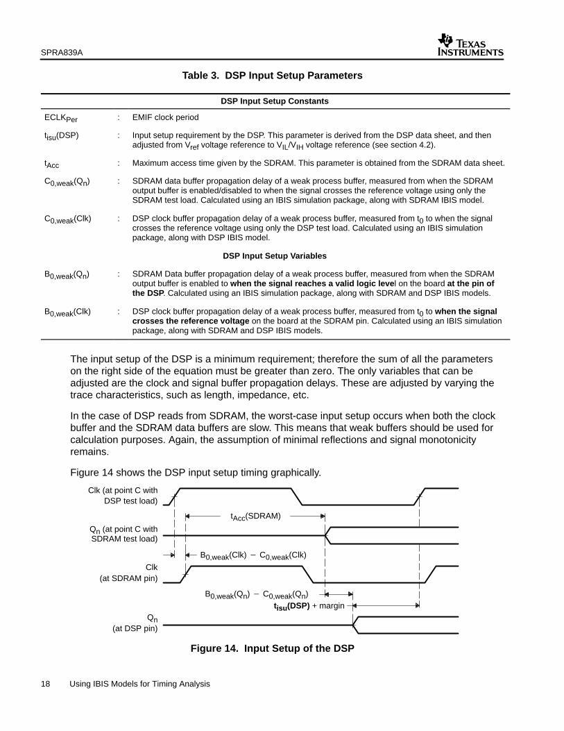
In the case of DSP reads from SDRAM, the worst-case input setup occurs when both the clockbuffer and the SDRAM data buffers are slow. This means that weak buffers should be used forcalculation purposes. Again, the assumption of minimal reflections and signal monotonicityremains.
Figure 14 shows the DSP input setup timing graphically.
tisu(DSP) + margin
Clk (at point C withDSP test load)
Qn (at point C withSDRAM test load)
Clk(at SDRAM pin)
Qn(at DSP pin)
B0,weak(Clk) � C0,weak(Clk)
tAcc(SDRAM)
B0,weak(Qn) � C0,weak(Qn)
Figure 14. Input Setup of the DSP
SPRA839A
19 Using IBIS Models for Timing Analysis
Because of the multiple data signals, each trace must be calculated (using the methoddiscussed above) to find the maximum difference between the board and test load. Thismaximum difference will result in the worst-case setup time to the DSP.
6.4 Input Hold of the DSP
To verify that hold times to the DSP are met, the margin defined in the following equation mustbe greater than zero.
margin �
�B0,strong (Qn)� C0,strong (Qn)� min � toh �
�B0,strong (Clk) � C0,strong (Clk)� � tih(DSP)
Tester Load Adjustmentfor Data Lines
Tester Load Adjustmentfor Clock Signal
The above variables and constants are described in Table 4.
Table 4. DSP Input Hold Parameters
DSP Input Hold Constants
tih(DSP) : Input hold requirement by the DSP. This parameter is derived from the DSP data sheet, and thenadjusted from Vref voltage reference to VIL/VIH voltage reference (see section 4.2).
toh : Minimum hold time given by the SDRAM. This parameter is obtained from the SDRAM data sheet.
C0,strong(Qn) : SDRAM data buffer propagation delay of a strong process buffer, measured from when the SDRAMoutput buffer is enabled/disabled to when the signal crosses the reference voltage using only theSDRAM test load. Calculated using an IBIS simulation package, along with SDRAM IBIS model.
C0,strong(Clk) : DSP clock buffer propagation delay of a strong process buffer, measured from t0 to when the signalcrosses the reference voltage using only the DSP test load. Calculated using an IBIS simulationpackage, along with DSP IBIS model.
DSP Input Hold Variables
B0,strong(Qn) : SDRAM data buffer propagation delay of a strong process buffer, measured from when the SDRAMdata buffer is disabled to the when the signal goes to an invalid logic level on the board at pin ofthe DSP. Calculated using an IBIS simulation package, along with DSP and SDRAM IBIS models.
B0,strong(Clk) : DSP clock buffer propagation delay of a strong process buffer, measured from t0 to when the signalcrosses the reference voltage on the board at the pin of the DSP. Calculated using an IBISsimulation package, along with DSP and SDRAM IBIS models.
The input hold of the DSP is a minimum requirement; therefore the sum of all the parameters onthe right side of the equation must be greater than zero. The only variables that can be adjustedare the clock and signal buffer propagation delays. These are adjusted by varying the tracecharacteristics.
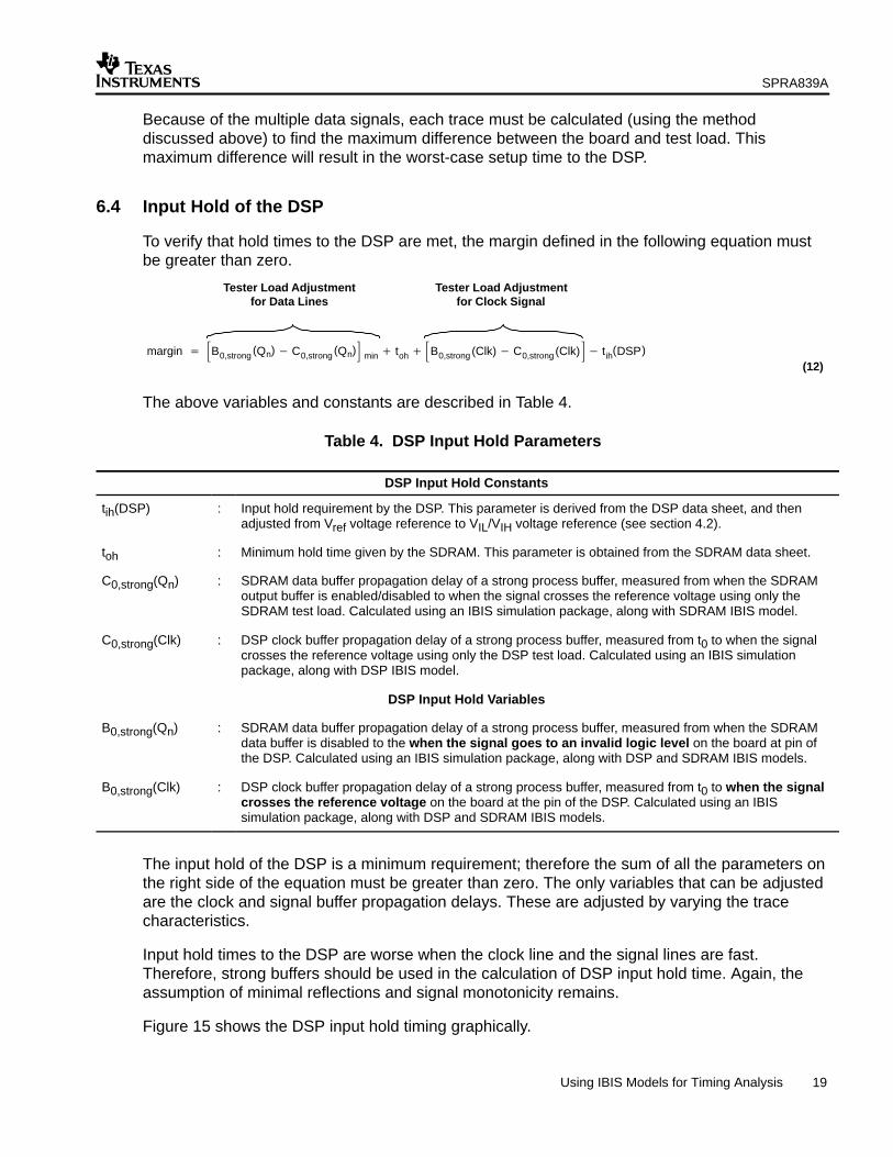
Input hold times to the DSP are worse when the clock line and the signal lines are fast.Therefore, strong buffers should be used in the calculation of DSP input hold time. Again, theassumption of minimal reflections and signal monotonicity remains.
Figure 15 shows the DSP input hold timing graphically.
(12)
SPRA839A
20 Using IBIS Models for Timing Analysis
Clk (at point C withDSP test load)
Qn (at point C withSDRAM test load)
Clk(at SDRAM pin)
Qn(at DSP pin)
B0,strong(Clk) � C0,strong(Clk)
toh(SDRAM)
tih(DSP) + margin
B0,strong(Qn) � C0,strong(Qn)
Figure 15. Input Hold of the DSP
Because of the multiple data signals, each trace must be calculated (using the methoddiscussed above) to find the minimum difference between the board and test load. Thisminimum difference will result in the worst-case hold time to the DSP.
7 Summary of AC Timing Analysis Procedures
This section provides a summary of the procedures for AC timing analysis according to themethod discussed in this application report. The subsections provide detailed explanation of thethree steps involved: gathering information, IBIS simulations, and analysis.
7.1 Gathering Information
The first step in AC timing analysis is to gather all of the relevant information, including:
1. Data sheets for the DSP and SDRAM
2. IBIS models for the DSP and SDRAM
3. Board layout and characteristics
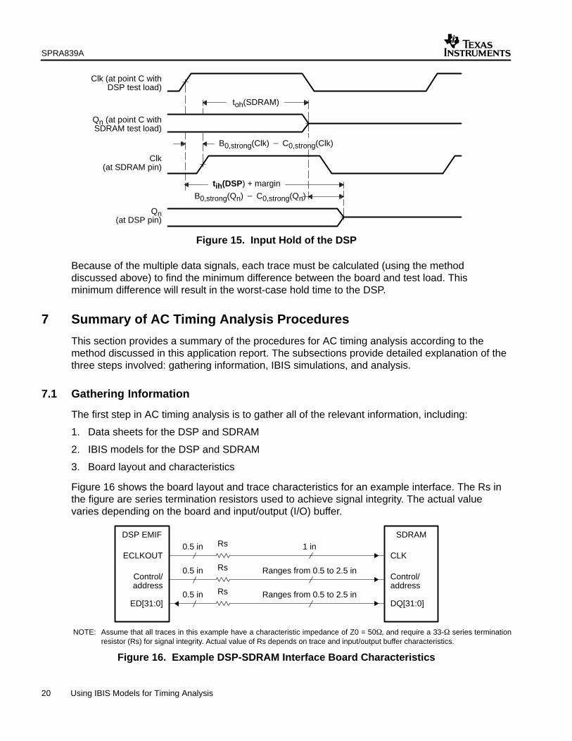
Figure 16 shows the board layout and trace characteristics for an example interface. The Rs inthe figure are series termination resistors used to achieve signal integrity. The actual valuevaries depending on the board and input/output (I/O) buffer.
Ranges from 0.5 to 2.5 inRs0.5 in
1 inRs0.5 in
Ranges from 0.5 to 2.5 inRs0.5 in
ECLKOUT
Control/address
ED[31:0]
CLK
Control/address
DQ[31:0]
DSP EMIF SDRAM
NOTE: Assume that all traces in this example have a characteristic impedance of Z0 = 50�, and require a 33-� series terminationresistor (Rs) for signal integrity. Actual value of Rs depends on trace and input/output buffer characteristics.
Figure 16. Example DSP-SDRAM Interface Board Characteristics
SPRA839A
21 Using IBIS Models for Timing Analysis
7.2 IBIS Simulations
Before performing IBIS simulations on the DSP-SDRAM interface, you should first modify theIBIS models’ VIL and VIH levels to account for noise margin, as discussed in section 5. Edit Vinlto 0.6 V, and Vinh to 2.5 V.
7.2.1 IBIS Simulations for DSP Outputs on the Board
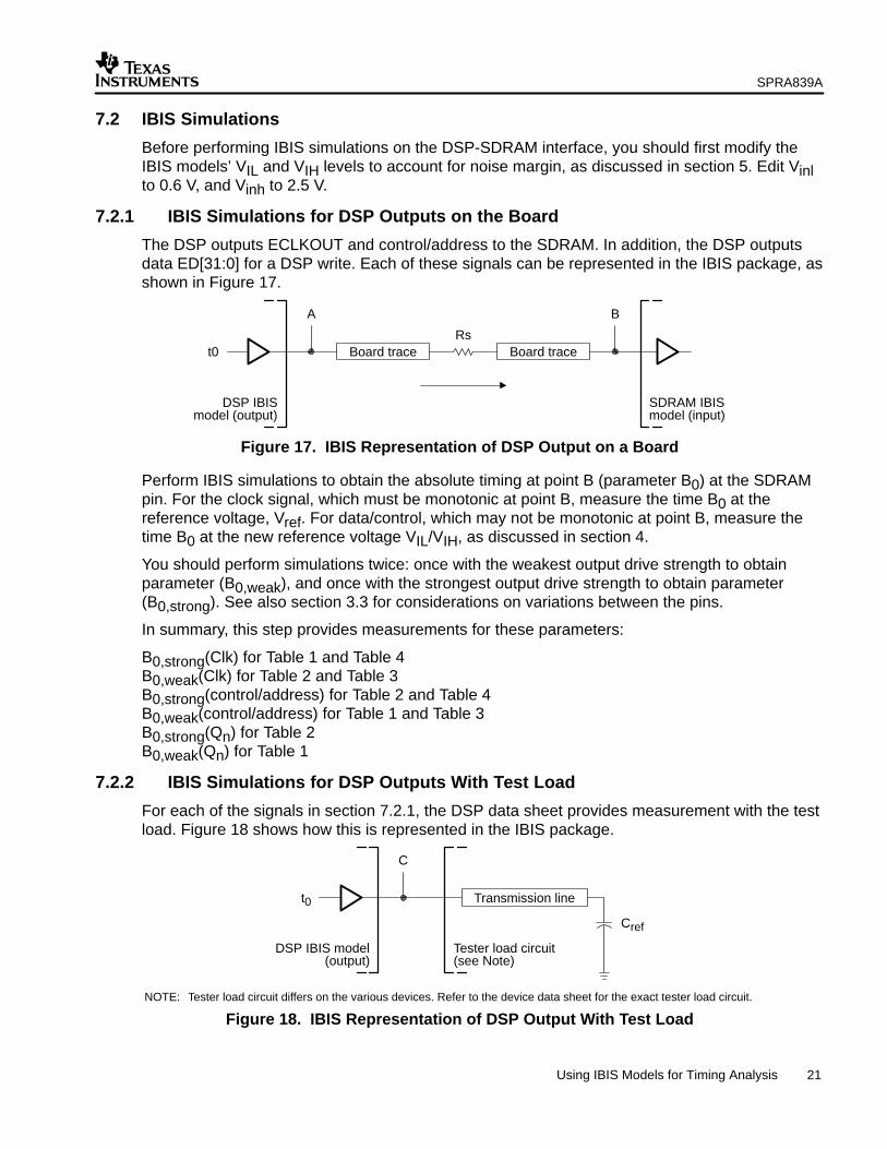
The DSP outputs ECLKOUT and control/address to the SDRAM. In addition, the DSP outputsdata ED[31:0] for a DSP write. Each of these signals can be represented in the IBIS package, asshown in Figure 17.
t0 Board trace
A
DSP IBISmodel (output)
RsBoard trace
B
SDRAM IBISmodel (input)
Figure 17. IBIS Representation of DSP Output on a Board
Perform IBIS simulations to obtain the absolute timing at point B (parameter B0) at the SDRAMpin. For the clock signal, which must be monotonic at point B, measure the time B0 at thereference voltage, Vref. For data/control, which may not be monotonic at point B, measure thetime B0 at the new reference voltage VIL/VIH, as discussed in section 4.
You should perform simulations twice: once with the weakest output drive strength to obtainparameter (B0,weak), and once with the strongest output drive strength to obtain parameter(B0,strong). See also section 3.3 for considerations on variations between the pins.
In summary, this step provides measurements for these parameters:
B0,strong(Clk) for Table 1 and Table 4B0,weak(Clk) for Table 2 and Table 3B0,strong(control/address) for Table 2 and Table 4B0,weak(control/address) for Table 1 and Table 3B0,strong(Qn) for Table 2B0,weak(Qn) for Table 1
7.2.2 IBIS Simulations for DSP Outputs With Test Load
For each of the signals in section 7.2.1, the DSP data sheet provides measurement with the testload. Figure 18 shows how this is represented in the IBIS package.
t0
C
Transmission line
Cref
Tester load circuit(see Note)
DSP IBIS model(output)
NOTE: Tester load circuit differs on the various devices. Refer to the device data sheet for the exact tester load circuit.
Figure 18. IBIS Representation of DSP Output With Test Load
SPRA839A
22 Using IBIS Models for Timing Analysis
Perform IBIS simulations to obtain the absolute timing at point C (parameter C0) with the DSPtest load. Measure the time C0 at the data sheet reference voltage, Vref.
You should perform simulations twice: once with the weakest output drive strength to obtainparameter (C0,weak), and once with the strongest output drive strength to obtain parameter(C0,strong). See also section 3.3 for considerations on variations between the pins.
In summary, this step provides measurements for these parameters:
C0,strong(Clk) for Table 1 and Table 4C0,weak(Clk) for Table 2 and Table 3C0,strong(control/address) for Table 2 and Table 4C0,weak(control/address) for Table 1 and Table 3C0,strong(Qn) for Table 2C0,weak(Qn) for Table 1
7.2.3 IBIS Simulations for SDRAM Outputs on the Board
The SDRAM outputs data DQ[31:0] for a DSP read. Each of these signals can be represented inthe IBIS package as shown in Figure 19.
Board trace
B
DSP IBISmodel (input)
RsBoard trace
A
SDRAM IBISmodel (output)
Figure 19. IBIS Representation of SDRAM Output on a Board
Perform IBIS simulations to obtain the absolute timing at point B (parameter B0) at the DSP pin.Because the data signal may not be monotonic at the DSP pin (point B), measure the time B0 atthe new reference voltage VIL/VIH, as discussed in section 4.
You should perform simulations twice: once with the weakest output drive strength to obtainparameter (B0,weak), and once with the strongest output drive strength to obtain parameter(B0,strong). See also section 3.3 for considerations on variations between the pins.
In summary, this step provides measurements for these parameters:
B0,strong(Qn) for Table 4B0,weak(Qn) for Table 3
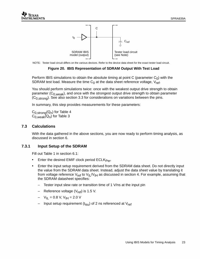
7.2.4 IBIS Simulations for SDRAM Outputs With Test Load
For the data signals in section 7.2.4, the SDRAM data sheet provides measurement with the testload. Figure 20 shows how this is represented in the IBIS package.
SPRA839A
23 Using IBIS Models for Timing Analysis
t0
C
Cref
SDRAM IBISmodel (output)
Tester load circuit(see Note)
NOTE: Tester load circuit differs on the various devices. Refer to the device data sheet for the exact tester load circuit.
Figure 20. IBIS Representation of SDRAM Output With Test Load
Perform IBIS simulations to obtain the absolute timing at point C (parameter C0) with theSDRAM test load. Measure the time C0 at the data sheet reference voltage, Vref.
You should perform simulations twice: once with the weakest output drive strength to obtainparameter (C0,weak), and once with the strongest output drive strength to obtain parameter(C0,strong). See also section 3.3 for considerations on variations between the pins.
In summary, this step provides measurements for these parameters:
C0,strong(Qn) for Table 4C0,weak(Qn) for Table 3
7.3 Calculations
With the data gathered in the above sections, you are now ready to perform timing analysis, asdiscussed in section 6.
7.3.1 Input Setup of the SDRAM
Fill out Table 1 in section 6.1:
• Enter the desired EMIF clock period ECLKPer.
• Enter the input setup requirement derived from the SDRAM data sheet. Do not directly inputthe value from the SDRAM data sheet. Instead, adjust the data sheet value by translating itfrom voltage reference Vref to VIL/VIH as discussed in section 4. For example, assuming thatthe SDRAM datasheet specifies:
– Tester input slew rate or transition time of 1 V/ns at the input pin
– Reference voltage (Vref) is 1.5 V.
– VIL = 0.8 V, VIH = 2.0 V
– Input setup requirement (tisu) of 2 ns referenced at Vref
SPRA839A
24 Using IBIS Models for Timing Analysis
The adjusted SDRAM input setup requirement referenced at VIL/VIH is calculated accordingto the formula in Figure 10:
t2 is a larger number, and therefore a more stringent new tisu requirement. Enter t2 into Table 1.
• Enter the tpd-max from the DSP data sheet.
• Enter the B0 and C0 parameters obtained in sections 7.2.1 and 7.2.2.
Then, calculate the SDRAM input setup margin using the formula in section 6.1.
7.3.2 Input Hold of the SDRAM
Fill out Table 2 in section 6.2:
• Enter the input hold requirement derived from the SDRAM data sheet. Do not directly inputthe value from the SDRAM data sheet. Instead, adjust the data sheet value by translating itfrom voltage reference Vref to VIL/VIH, as discussed in section 4.
• Enter the tpd-min from the DSP data sheet.
• Enter the B0 and C0 parameters obtained in sections 7.2.1 and 7.2.2.
Then, calculate the SDRAM input hold margin using the formula in section 6.2.
7.3.3 Input Setup of the DSP
Fill out Table 3 in section 6.3:
• Enter the desired EMIF clock period ECLKPer.
• Enter the input setup requirement derived from the DSP data sheet. Do not directly input thevalue from the DSP data sheet. Instead, adjust the data sheet value by translating it fromvoltage reference Vref to VIL/VIH, as discussed in section 4.
• Enter the tAcc from the SDRAM data sheet.
• Enter the B0 and C0 parameters obtained in sections 7.2.1 through 7.2.4.
Then, calculate the DSP input setup margin using the formula in section 6.3.
7.3.4 Input Hold of the DSP
Fill out Table 4 in section 6.4:
• Enter the input hold requirement derived from the DSP data sheet. Do not directly input thevalue from the DSP data sheet. Instead, adjust the data sheet value by translating it fromvoltage reference Vref to VIL/VIH, as discussed in section 4.
• Enter the toh from the SDRAM data sheet.
• Enter the B0 and C0 parameters obtained in sections 7.2.1 through 7.2.4.
Then, calculate the DSP input hold margin using the formula in section 6.4.
SPRA839A
25 Using IBIS Models for Timing Analysis
8 Conclusion
Using the equations discussed in this application report, IBIS models and simulations can beused to reflect timings for point-to-point connections between an SDRAM and a DSP. Iterationson these equations may be necessary to obtain desired signal integrity and the proper timingsfor both setup and hold to the SDRAM and the DSP. This technique is not limited to SDRAMs orthe EMIF interface. All DSP signals have characteristic setup and hold times that must beadhered to. Using the techniques discussed in this application report, IBIS analysis can used todetermine proper timing relations for all relevant signals.
An understanding of the tester is needed to properly back calculate timings, to correct forvariations in loading on the signals. Noise level margins can be accounted for by modifying thevalid logic levels. The equations discussed in this application report give a representation of howmuch margin can be expected. Acceptable margin levels must be determined based on systemenvironment and operating conditions.
IMPORTANT NOTICE
Texas Instruments Incorporated and its subsidiaries (TI) reserve the right to make corrections, modifications,enhancements, improvements, and other changes to its products and services at any time and to discontinueany product or service without notice. Customers should obtain the latest relevant information before placingorders and should verify that such information is current and complete. All products are sold subject to TI’s termsand conditions of sale supplied at the time of order acknowledgment.
TI warrants performance of its hardware products to the specifications applicable at the time of sale inaccordance with TI’s standard warranty. Testing and other quality control techniques are used to the extent TIdeems necessary to support this warranty. Except where mandated by government requirements, testing of allparameters of each product is not necessarily performed.
TI assumes no liability for applications assistance or customer product design. Customers are responsible fortheir products and applications using TI components. To minimize the risks associated with customer productsand applications, customers should provide adequate design and operating safeguards.
TI does not warrant or represent that any license, either express or implied, is granted under any TI patent right,copyright, mask work right, or other TI intellectual property right relating to any combination, machine, or processin which TI products or services are used. Information published by TI regarding third–party products or servicesdoes not constitute a license from TI to use such products or services or a warranty or endorsement thereof.Use of such information may require a license from a third party under the patents or other intellectual propertyof the third party, or a license from TI under the patents or other intellectual property of TI.
Reproduction of information in TI data books or data sheets is permissible only if reproduction is withoutalteration and is accompanied by all associated warranties, conditions, limitations, and notices. Reproductionof this information with alteration is an unfair and deceptive business practice. TI is not responsible or liable forsuch altered documentation.
Resale of TI products or services with statements different from or beyond the parameters stated by TI for thatproduct or service voids all express and any implied warranties for the associated TI product or service andis an unfair and deceptive business practice. TI is not responsible or liable for any such statements.