400
Using the ELECTRIC VLSI Design System Version 9.07 Steven M. Rubin

Using the
ELECTRIC
VLSI Design System
Version 9.07
Steven M. Rubin

Author's affiliation:
Static Free Software
ISBN 0−9727514−3−2
Published by R.L. Ranch Press, 2016.
Copyright (c) 2016 Static Free Software
Permission is granted to make and distribute verbatim copies of this book provided the copyright notice andthis permission notice are preserved on all copies.
Permission is granted to copy and distribute modified versions of this book under the conditions for verbatimcopying, provided also that they are labeled prominently as modified versions, that the authors' names andtitle from this version are unchanged (though subtitles and additional authors' names may be added), and thatthe entire resulting derived work is distributed under the terms of a permission notice identical to this one.
Permission is granted to copy and distribute translations of this book into another language, under the aboveconditions for modified versions.
Electric is distributed by Static Free Software (staticfreesoft.com), a division of RuLabinsky Enterprises,Incorporated.

Table of ContentsChapter 1: Introduction.....................................................................................................................................1
1−1: Welcome.........................................................................................................................................11−2: About Electric.................................................................................................................................21−3: Running Electric..............................................................................................................................31−4: Building Electric from Source Code...............................................................................................51−5: Plug−Ins........................................................................................................................................101−6: Fundamental Concepts..................................................................................................................121−7: The Display...................................................................................................................................151−8: The Mouse.....................................................................................................................................171−9: The Keyboard................................................................................................................................181−10: IC Layout Tutorial.......................................................................................................................211−11: Schematics Tutorial.....................................................................................................................301−12: Schematics and Layout Tutorial..................................................................................................36
Chapter 2: Basic Editing..................................................................................................................................472−1: Selection........................................................................................................................................472−2: Circuit Creation.............................................................................................................................522−3: Circuit Deletion.............................................................................................................................572−4: Circuit Modification......................................................................................................................592−5: Changing Size...............................................................................................................................632−6: Changing Orientation....................................................................................................................65
Chapter 3: Hierarchy.......................................................................................................................................673−1: Cells...............................................................................................................................................673−2: Cell Creation and Deletion............................................................................................................693−3: Creating Instances.........................................................................................................................713−4: Examining Cell Instances..............................................................................................................733−5: Moving Up and Down the Hierarchy............................................................................................743−6: Exports..........................................................................................................................................763−7: Cell Information............................................................................................................................823−8: Rearranging Cell Hierarchy..........................................................................................................873−9: Libraries........................................................................................................................................883−10: Copying Cells Between Libraries...............................................................................................953−11: Views...........................................................................................................................................97
Chapter 4: Display..........................................................................................................................................1014−1: The Tool Bar...............................................................................................................................1014−2: The Messages Window...............................................................................................................1034−3: Creating and Deleting Editing Windows....................................................................................1044−4: Zooming and Panning.................................................................................................................1084−5: The Sidebar.................................................................................................................................1114−6: Color............................................................................................................................................1194−7: Grids and Alignment...................................................................................................................1234−8: Printing........................................................................................................................................127
Using the Electric VLSI Design System, version 9.07 i

Table of Contents4−9: Text Windows.............................................................................................................................1294−10: 3D Windows..............................................................................................................................1314−11: Waveform Windows.................................................................................................................137
Chapter 5: Arcs...............................................................................................................................................1455−1: Introduction to Arcs....................................................................................................................1455−2: Constraints...................................................................................................................................1465−3: Setting Constraints......................................................................................................................1495−4: Other Properties..........................................................................................................................1505−5: Default Arc Properties.................................................................................................................153
Chapter 6: Advanced Editing........................................................................................................................1556−1: Making Copies............................................................................................................................1556−2: Creation Defaults........................................................................................................................1566−3: Preferences..................................................................................................................................1586−4: Making Arrays............................................................................................................................1606−5: Spreading Circuitry.....................................................................................................................1626−6: Replacing Circuitry.....................................................................................................................1636−7: Undo Control...............................................................................................................................1656−8: Text.............................................................................................................................................1666−9: Networks.....................................................................................................................................1756−10: Outlines.....................................................................................................................................1826−11: Interpretive Languages..............................................................................................................1866−12: Project Management..................................................................................................................1906−13: CVS Project Management.........................................................................................................1946−14: Emergencies..............................................................................................................................196
Chapter 7: Technologies................................................................................................................................1977−1: Introduction to Technologies......................................................................................................1977−2: Scaling and Units........................................................................................................................2017−3: I/O Control..................................................................................................................................2037−4: The MOS Technologies..............................................................................................................2197−5: Schematics...................................................................................................................................2237−6: Special Technologies..................................................................................................................228
Chapter 8: Creating New Technologies........................................................................................................2398−1: Technology Editing.....................................................................................................................2398−2: Converting between Technologies and Libraries........................................................................2418−3: Hierarchies of Technology Libraries..........................................................................................2438−4: The Layer Cells...........................................................................................................................2448−5: The Arc Cells..............................................................................................................................2488−6: The Node Cells............................................................................................................................2508−7: Miscellaneous Information..........................................................................................................2558−8: How Technology Changes Affect Existing Libraries.................................................................257
ii Using the Electric VLSI Design System, version 9.07

Table of Contents8−9: Examples of Use.........................................................................................................................2598−10: Technology XML File Format..................................................................................................2638−11: The Technology Creation Wizard.............................................................................................278
Chapter 9: Tools.............................................................................................................................................2879−1: Introduction To Tools.................................................................................................................2879−2: Design Rule Checking (DRC).....................................................................................................2899−3: Electrical Rule Checking (ERC).................................................................................................2969−4: Simulation Interface....................................................................................................................2989−5: Simulation (built−in)...................................................................................................................3129−6: Routing........................................................................................................................................3269−7: Network Consistency Checking (NCC)......................................................................................3389−8: Generation...................................................................................................................................3579−9: Logical Effort..............................................................................................................................3679−10: Extraction..................................................................................................................................3719−11: Compaction...............................................................................................................................3759−12: Silicon Compiler.......................................................................................................................3769−13: Placement..................................................................................................................................379
Chapter 10: The JELIB and DELIB File Format.......................................................................................38110−1: Introduction to File Format.......................................................................................................38110−2: Header.......................................................................................................................................38310−3: Body..........................................................................................................................................38610−4: Miscellaneous............................................................................................................................391
Using the Electric VLSI Design System, version 9.07 iii

iv Using the Electric VLSI Design System, version 9.07

Chapter 1: Introduction
1−1: Welcome
Now you have it!
A state−of−the−art computer−aided design system for VLSI circuit design.
Electric designs MOS and bipolar integrated circuits, printed−circuit−boards, or any type of circuit youchoose. It has many editing styles including layout, schematics, artwork, and architectural specifications.
A large set of tools is available including design−rule checkers, simulators, routers, layout generators, andmore.
Electric interfaces to most popular CAD specifications including EDIF, LEF/DEF, VHDL, CIF and GDS.
The most valuable aspect of Electric is its layout−constraint system, which enables top−down design byenforcing consistency of connections.
This manual explains the concepts and commands necessary to use Electric. It begins with essential featuresand builds on them to explain all aspects of the system. As with any computer system manual, the reader isencouraged to have a machine handy and to try out each operation.
Using the Electric VLSI Design System, version 9.07 1

1−2: About Electric
The About Electric... command (in menu Help) shows you the names of the Electric development team. Italso outlines your legal rights with respect to Electric.
This manual is available while running Electric. Use the User's Manual... command (in menu Help) to seethis manual (you may already be doing that).
While inside of the manual, click "Menu Help" to get help with Electric's pulldown menus. It displays apulldown menu inside of the manual page which mimics the real pulldown menu. Select any command fromthis new menu to get help for the real pulldown menu entry.
Chapter 1: Introduction
2 Using the Electric VLSI Design System, version 9.07

1−3: Running Electric
There are two ways to run Electric:
Download the JAR file from GNU. This is discussed further below.• Build Electric from source code. This is discussed in Section 1−4−1.•
Downloading the Electric JAR file is explained here. Electric is written in the Java programming languageand so the JAR file is typically called "electric−version.jar" where version is 8.09, 8.10, 9.00, 9.01, etc. Thereare two variations on the JAR file: with or without source code (the version without source code has the word"Binary" in its name). Either of these files can run Electric, but the one with source code is larger because italso has all of the Java code.
Electric requires OpenJDK, Apache Harmony, or Oracle Java version 1.6. It is developed with Oracle Java,so if you run into problems with other versions, try installing Java 1.6 or later from Oracle.
Running Electric varies with the different platforms. Most systems also allow you to double−click on theJAR file. If double−clicking doesn't work, try running it from the command−line by typing either:
java −jar electric−version.jar [libraries]
or:java −classpath electric−version.jar com.sun.electric.Launcher [libraries]
There are a number of options that can be given at the end of the command line:
−mdi force a multiple document interface style (where Electric is one big window with smaller editwindows in it). This is the default interface on Windows.
•
−sdi force a single document interface style (where each Electric window is separate). This is thedefault interface on UNIX/GNU−Linux and the Macintosh. Note that the MDI/SDI settings can alsobe made from the Display Control Preferences (see Section 4−3).
•
−s script run the script file through the Bean Shell. If the script is "−" then the script is read from thestandard input.
•
−batch run in batch mode (no windows or other user interface are shown; batch mode implies 'noGUI', and nothing more).
•
−version provides full version information including the build date.• −v provides brief version information.• −NOMINMEM ignores minimum memory requirements when starting the JVM.• −help prints a list of available command options.• −debug adds developer menus and other debugging state. One of the debug menus is "Test" whichlets Electric test itself. The test data is available for download atwww.staticfreesoft.com/ElectricRegressionData.zip. After extracting the data, you must set itslocation in the "Tests" Preferences.
•
Chapter 1: Introduction
Using the Electric VLSI Design System, version 9.07 3

Memory Control
One problem with Java is that the Java Virtual Machine has a memory limit. This limit prevents programsfrom growing too large. However, it prevents large circuits from being edited.
If Electric runs out of memory, you can request more. To do this, use the General Preferences (in menu File /Preferences..., "General" section, "General" tab). The "Memory" section has two memory limit fields, forMaximum memory and Maximum permanent space. Changes to these values take effect when you next runElectric. Note that any request to expand Electric beyond the default Java sizes will cause Electric tore−launch itself at startup so that the JVM has access to more memory. To prevent relaunching of Electric,set the memory fields back to zero.
The Maximum memory size is the most important because increasing it will offer much more circuitrycapacity. Note that 32−bit JVMs can only grow so far. On 32−bit Windows systems you should not set itabove 1500 (1.5 Gigabytes). On 32−bit Linux or Macintosh system, you should not set it above 3600 (3.6Gigabytes).
Permanent space is an additional section of memory that may need to be increased. For very large chips, avalue of 200 or more may enhance performance.
Chapter 1: Introduction
4 Using the Electric VLSI Design System, version 9.07

1−4: Building Electric from Source Code
1−4−1: Introduction to Source Code
It is not necessary to build Electric from the source code because the downloads are ready to run. For peoplewho wish to explore the source code, this section describes how you can do it.
Source code is available in two forms:
Packaged in the JAR file. The Electric download from the Free Software Foundation (GNU) hassource code in it which you can extract to build Electric. See Section 1−4−2 for more. Note that thismethod is not the preferred way to access the Electric source code because it does not handledependencies.
•
At savannah.gnu.org. The Electric source code is in a repository at savannah.gnu.org, specificallyhere. There are a number of ways to build Electric from the source code:
Using the command−line (see Section 1−4−3).♦ Using the Netbeans development environment (see Section 1−4−4).♦ Using the Eclipse development environment (see Section 1−4−5).♦
•
1−4−2: Source Code in the JAR Files
Two Electric downloads are available from the Free Software Foundation (GNU): with and without sourcecode. Therefore it is possible to build Electric from the source code in the download. Note, however, that thisis not the preferred way to access the source code because it does not include the various dependencies. Thepreferred way to access the source code is to use Subversions and to access the code on savannah.gnu.org(see the next three sections for more).
To extract the source code from the ".jar" file, place it in its own directory, change to that directory, and runthe following command:
jar xf electric−version.jar
(Windows users may want to install "cygwin," from www.cygwin.com, in order to more easily run "jar" andother commands.) The "jar" command will create a number of files and folders on your disk:
com is a folder with all of the source code.• org and scala are folders with additional source code that isn't needed when rebuilding.• META−INF is a support folder used when running the ".jar" file and can be deleted.• ChangeLog.txt is a detailed list of changes to Electric.• COPYING.txt is the GNU copyright document that applies to your use of Electric.• README.txt is a file of notes about Electric.•
Chapter 1: Introduction
Using the Electric VLSI Design System, version 9.07 5

The next step is to get a version of Java that can build source code. Although a "JRE" (Java RuntimeEnvironment) is sufficient for running Electric, it is not able to build the source code. For that, you must havea "JDK" (Java Development Kit). In addition, you may want to use an IDE (Integrated DevelopmentEnvironment) such as NetBeans (at www.netbeans.org) or Eclipse (at www.eclipse.org).
Using the Command Line
"Ant" is a scripting system for building Java programs, and Electric comes with an Ant script called"build.xml". Once the source code is extracted, you can rebuild Electric simply by typing "ant". Before youdo that, there are some considerations:
If you are not on a Macintosh, you must obtain the Apple Java Extensions fromdeveloper.apple.com/samplecode/AppleJavaExtensions and place it in the directory (next to the"build.xml" file).
•
The build script only builds what is on your disk. If you want to include the Static Free Softwareextensions, you must download it and extract it before building.
•
The build script does not include the parts of Electric that are coded in Scala (insignificant).• The build script does not build the Bean Shell or Jython.•
Running under Eclipse
Here are some notes about building Electric under Eclipse:
Setup Workspace. The Workspace is a point in the file system where all source code can be found.You can use the directory where you extracted the Electric source code, or any point above that.
•
Create Project. The Project defines a single program that is being built. Use File / New /Project and choose "Java Project from Existing Ant Buildfile". Choose the "build.xml" file in thefolder where the files were extracted. Give the project a name, for example, "Electric."
•
Configure Libraries. The "Libraries" tab of the Eclipse project settings lets you add other packagesthat may be relevant to the build. There are no required libraries, but many optional ones (see Section1−5 on plug−ins). Use the "Add External JARs" button to add any extra libraries.
•
Handle Macintosh variations. If you are building on a Macintosh, no changes are needed. If youare not building on a Macintosh, you must decide whether or not you want the code that you produceto also run on a Macintosh. If you do not care about being able to run on a Macintosh, remove thesource code module "com.sun.electric.tool.user.MacOSXInterface.java" (which probably has a red"X" next to it indicating that there are errors in the file). If you want the final code to be able to runon all platforms, download the stub package "AppleJavaExtensions.jar" fromdeveloper.apple.com/samplecode/AppleJavaExtensions and add this as an external JAR file.
•
Run Electric. Use the Run... command (under the Run menu) to create a run configuration. Underthe "Main" tab of the run−configuration dialog, give the configuration a name (for example,"Electric"), set the Project to match the one that you have created, and set the "Main class" to be"com.sun.electric.Launcher". Under the "Arguments" section of the dialog, it is a good idea toincrease Electric's memory size by entering "−mx1000m" under "VM arguments".
•
Chapter 1: Introduction
6 Using the Electric VLSI Design System, version 9.07

1−4−3: Command−line Access to the savannah.gnu.org Repository
Before attempting to build Electric from the savannah.gnu.org, you must have these tools installed on yourcomputer:
JDK 1.6 or later (a JRE is sufficient for running Electric, but a JDK is necessary to build it).1. Subversion. This is the source−code control system.2. Apache Ant 1.8.0 or later.3.
The following variable should be defined:JAVA_PATH path to JDK root directory
Next, download the latest sources using Subversion. The first time you do this, issue these commands:cd WORK−DIR
svn checkout svn://svn.savannah.gnu.org/electric
cd electric
Once the code has been downloaded, it can be updated with these commands:cd WORK−DIR/electric
svn update
Next, compile the sources (it takes longer the first time, but works incrementally after that):cd WORK−DIR/electric/packaging
ant
Next run Electric (note that the "X.XX" should be replaced with the current version, for example "9.01"):WORK−DIR/electric/packaging/electricPublic−X.XX.jar
or:java −jar WORK−DIR/electric/packaging/electricPublic−X.XX.jar
or:java −classpath WORK−DIR/electric/packaging/electricPublic−X.XX.jar
com.sun.electric.Launcher
If your design is large and you need more memory, you can request a larger heap size with this command:java −classpath WORK−DIR/electric/packaging/electricPublic−X.XX.jar
com.sun.electric.Launcher −Xmx1024m −XX:MaxPermSize=128m
Chapter 1: Introduction
Using the Electric VLSI Design System, version 9.07 7

1−4−4: Netbeans Access to the savannah.gnu.org Repository
Start NetBeans 7.0 or later (these instructions do not work with earlier versions).1. Install the Team Server Plugin (may be done already with some NetBeans installations):
Use Tools / Plugins and choose the "Available Plugins" tab in the Plugins manager.♦ In the left pane, check the "Team Server" plugin and click "Install". If it is not listed, then itmay already be installed.
♦
Use Window / Services to open the "Services" tab♦ Expand the "Team Server" node and check that the "savannah.gnu.org" Team Server is listed.♦
2.
Download Electric Sources from savannah.gnu.org . Use Team / Team Server / savannah.gnu.org and click Open Project♦ Search for "electric", select "Electric: VLSI Design System", and click "Open From TeamServer"
♦
Expand the "Electric: VLSI Design System" node in the "Team" tab and the "Sources"subnode
♦
Click "Source Code Repository (get)"♦ Either enter "Folder To Get" or click the "Browse..." button and choose "trunk" .♦ Choose "Local Folder" and select the location for Electric Sources. The default is"~/NetBeansProjects/electric~svn"
♦
Click "Get From Team Server"♦ When done, the "Checkout Completed" dialog will say that projects were checked−out. Click"Open Project...", choose "electric", and click "Open".
♦
3.
Build Electric Click Run / Set Project Configuration / release−profile. ♦ In the "Projects" tab, right−click "electric" and choose "Build". The Electric project is large.If the build hangs, then it may be necessary to add "−J−Xmx2g" to thenetbeans_default_options in file <NETBEANS_INSTALLATION>/etc/netbeans.conf .
♦
4.
Run Electric. Use either Run / Run Main Project (electric) or Debug / Debug Main Project(electric) from the main menu.
♦ 5.
Create a shortcut to start Electric from Desktop: Create a shortcut to "~/NetBeansProjects/electric~svn/electric/dist/electric.jar" in Unix or to"LocalFolder\Documents\NetBeansProjects\electric~svn\trunk\electric\target\electric−V.VV−n−SNAPSHOT−jar−with−dependencies.jar"in Windows
♦
Edit shortcut's "OpenWith" to OpenJDK or other Java distribution. Make this shortcutexecutable.
♦
Launch Electric with this shortcut.♦
6.
Create electric distribution for your organization (optional). Copy the folder ~/NetBeansProjects/electric~svn/electric/dist (with subdirectories) to ashared location in your file system.
♦ 7.
Chapter 1: Introduction
8 Using the Electric VLSI Design System, version 9.07

1−4−5: Eclipse Access to the savannah.gnu.org Repository
Install Eclipse: Install from www.eclipse.org. The instructions use the "Juno" or later version.♦ Because compiling Electric consumes more than average memory, edit the file eclipse.ini inthe installed area and change the last line from −Xmx512m to −Xmx1024.
♦
1.
Add Subversions to Eclipse: Do: Help / Install New Software♦ Work with http://subclipse.tigris.org/update_1.6.x♦
2.
Add Scala to Eclipse: Do: Help / Install New Software♦ Work with http://download.scala−ide.org/sdk/e38/scala29/stable/site (check all 3)♦
3.
Download Electric: Do: File / Import♦ Choose: SVN / Checkout Projects from SVN♦ Repository is: svn+ssh://[email protected]/electric/trunk Select thetop−level When asked, choose "Check out as a project in the workspace" and name it"Electric"
♦
4.
Make two Electric projects, one for Java code, one for Scala code: Do: File / New / Java Project♦ Browse to: Electric/electric−java♦ Set output to: electric−java/bin♦ Set external libraries to these JAR files in the "packaging" folder: AppleJavaExtensions−1.4,scala−library−2.9.1.jar, slf4j−api−1.6.2, slf4j−jdk14−1.6.2, j3dcore, j3dutils, vecmath,jmf.jar, bsh−2.0b4, jython.jar
♦
Do: File / New / Java Project♦ Browse to: Electric/electric−scala♦ Set output to: electric−scala/bin♦ Set external libraries to these JAR files in the "packaging" folder: slf4j−api−1.6.2,slf4j−jdk14−1.6.2
♦
Right−click on "electric−scala" project and choose "Configure / Add Scala Nature" ♦
5.
Link the two Electric projects: Right−click the "electric−scala" project, choose Properties, then Java Build Path Under the"Projects" tab, click "Add..." and add the "electric−java" project.
♦
Right−click the "electric−java" project, choose Properties, then Java Build Path Under the"Libraries" tab, click "Add Class Folder" and choose "electric−scala/bin".
♦
6.
Make a launch configuration: Do: Run / Run configurations♦ Create a new launch configuration (icon in upper−left)♦ In the Main tab, set the project to electric and the main class to com.sun.electric.Launcher♦ In the Arguments tab, set the VM arguments to −mx1200m (to request a 1.2GB JVM)♦
7.
Chapter 1: Introduction
Using the Electric VLSI Design System, version 9.07 9

1−5: Plug−Ins
Electric plug−ins are additional pieces of code that can be downloaded separately to enhance the system'sfunctionality. If you are building from the savannah.gnu.org repository, then all of these plug−ins are alreadyavailable. If, however, you are running from the GNU download, then these plugins are not present and mustbe downloaded separately.
Currently, these plug−ins are available:
Static Free Software extras (IRSIM, Animation) This plugin contains all of the pieces of Electric,written by Static Free Software, that are unable to be packaged with the GNU download (forlicensing reasons). It includes the IRSIM simulator and interfaces to the 3D Animation options. TheIRSIM simulator is a gate−level simulator from Stanford University. Although originally written inC, it was translated to Java so that it could plug into Electric. The Static Free Software extras areavailable from Static Free Software at www.staticfreesoft.com/electricSFS−9.07.jar.
•
Bean Shell The Bean Shell can be added to Electric to enable Java scripting and parameterevaluation. Advanced operations that make use of cell parameters will need this plug−in. The BeanShell is available from www.beanshell.org.
•
Jython Jython can be added to Electric to enable Python scripting. Jython is available fromwww.jython.org. Build a "standalone" installation to create a JAR file that can be used with Electric.
•
3D The 3D facility lets you view an integrated circuit in three−dimensions. It requires the Java3Dpackage, which is available from the Java Community Site, www.j3d.org. This is not a plugin, butrather an enhancement to your Java installation. Please note that if you are using a 64−bit version ofJava, you must install a 64−bit version of Java3D. Also note that your video card driver must supportOpenGL 1.2 or later in order for Java3D to work.
•
Animation Another extra that can be added to the 3D facility is 3D animation. This requires the JavaMedia Framework (JMF). The Java Media Framework is available from Oracle atjava.sun.com/products/java−media/jmf (this is not a plugin: it is an enhancement to your Javainstallation).
•
To attach a plugin, it must be in the CLASSPATH. The simplest way to do that is to invoke Electric from thecommand line, and specify the classpath. For example, to add the beanshell (a file named "bsh−2.0b1.jar"),type: java −classpath electric.jar:bsh−2.0b1.jar com.sun.electric.Launcher
Note that you must explicitly mention the main Electric class (com.sun.electric.Launcher) when usingplug−ins since all of the jar files are grouped together as the "classpath".
Chapter 1: Introduction
10 Using the Electric VLSI Design System, version 9.07

On Windows, you must use the ";" to separate jar files, and you might also have to quote the collection since";" separates commands: java −classpath "electric.jar;bsh−2.0b1.jar" com.sun.electric.Launcher
The above text can be placed into a ".bat" file to make a double−clickable Electric launch. You can also addJava switches and special Electric controls mentioned in Section 1−3. For example, to add in the SFSextension and extend the memory to 1GB, you can put this line in the ".bat" file: java −classpath "electric.jar;electricSFS.jar" −mx1000m com.sun.electric.Launcher
To find out which plugins are installed, click the "Plugins" button in the "About Electric..." dialog (in menuHelp).
Chapter 1: Introduction
Using the Electric VLSI Design System, version 9.07 11

1−6: Fundamental Concepts
MOST CAD SYSTEMS use two methods to do circuit design: connectivity and geometry.
The connectivity approach is used by every Schematic design system: you place components anddraw connecting wires. The components remain connected, even when they move.
•
The geometry approach is used by most Integrated Circuit (IC) layout systems: rectangles of "paint"are laid down on different layers to form the masks for chip fabrication.
•
ELECTRIC IS DIFFERENT because it uses connectivity for all design, even IC layout. This means that youplace components (MOS transistors, contacts, etc.) and draw wires (metal−2, polysilicon, etc.) to connectthem. The screen shows the true geometry, but it knows the connectivity too.
The advantages of connectivity−based IC layout are many:
No node extraction. Node extraction is not a separate, error−prone step. Instead, the connectivity ispart of the layout description and is instantly available. This speeds up all network−orientedoperations, including simulation, layout−versus−schematic (LVS), and electrical rules checkers.
•
No geometry errors. Complex components are no longer composed of unrelated pieces of geometrythat can be moved independently. In paint systems, you can accidentally move the gate geometryaway from a transistor, thus deleting the transistor. In Electric, the transistor is a single component,and cannot be accidentally destroyed.
•
More powerful editing. Browsing the circuit is more powerful because the editor can show theentire network whenever part of it is selected. Also, Electric combines the connectivity with a layoutconstraint system to give the editor powerful manipulation tools. These tools keep the designwell−connected, even as the circuit is modified on different levels of hierarchy.
•
Tools are smarter when they can use connectivity information. For example, the Design Rulechecker knows when the layout is connected and uses different spacing rules.
•
Simpler design process. When doing schematics and layout at the same time, getting a correct LVStypically involves many steps of design rule cleaning. This is because node extraction must be doneto obtain the connectivity of the IC layout, and node extractors cannot work when the design rulesare bad. So, each time LVS problems are found, the layout must be fixed and made DRC clean again.Since Electric can extract connectivity for LVS without having perfect design rules, the first step isto get the layout and schematics to match. Then the design rules can be cleaned−up without fear oflosing the LVS match.
•
Common user interface. One CAD system, with a single user interface, can be used to do both IClayout and schematics. Electric tightly integrates the process of drawing separate schematics and hasan LVS tool to compare them.
•
Chapter 1: Introduction
12 Using the Electric VLSI Design System, version 9.07

The disadvantages of connectivity−based IC layout are also known:
It is different from all the rest and requires retraining. This is true, but many have converted andfound it worthwhile. Users who are familiar with paint−based IC layout systems typically have aharder time learning Electric than those with no previous IC design experience.
•
Requires extra work on the user's part to enter the connectivity as well as the geometry. While thismay be true in the initial phases of design, it is not true overall. This is because the use ofconnectivity, early in the design, helps the system to find problems later on. In addition, Electric hasmany power tools for automatically handling connectivity.
•
Design is not WYSIWYG (what−you−see−is−what−you−get) because objects that touch on thescreen may or may not be truly connected. Electric has many tools to ensure that the connectivity hasbeen properly constructed.
•
The way that Electric handles all types of circuit design is by viewing it as a collection of nodes and arcs,woven into a network.
The nodes are electrical components suchas transistors, contacts, and logic gates.Arcs are simply wires that connect twocomponents. Ports are the connectionsites on nodes where the wires connect.
In the above example, the transistor node on the left has three pieces of geometry on different layers:polysilicon, active, and well. This node can be scaled, rotated, and otherwise manipulated without concernfor specific layer sizes. This is because rules for drawing the node have been coded in a technology, whichdescribes nodes and arcs in terms of specific layers.
Because Electric uses nodes and arcs for design, it is important that they be used to make all of the relevantconnections. Although layout may appear to be connected when two components touch, a wire must still beused to indicate the connectivity to Electric. This requires a bit more effort when designing a circuit, but thateffort is paid back in the many ways that Electric understands your circuit.
Besides creating meaningful electrical networks, arcs which form wires in Electric can also hold constraints.A constraint helps to control geometric changes, for example, the rigid constraint holds two components in afixed configuration while the rest of the circuit stretches. These constraints propagate through the circuit,even across hierarchical levels of design, so that very complex circuits can be intelligently manipulated.
A cell is a collection of these nodes and arcs, forming a circuit description. There can be different views of acell, such as the schematic, layout, icon, etc. Also, each view can have different versions, forming a historyof design. Multiple views and versions of a cell are organized into Cell groups.
For example, a clock cell may consist of a schematic view and a layout view. The schematic view may havetwo versions: 1 (older) and 2 (newer). In such a situation, the clock cell group contains 3 cells: the layout
Chapter 1: Introduction
Using the Electric VLSI Design System, version 9.07 13

view called "clock{lay}", the current schematic view called "clock{sch}", and the older schematic viewcalled "clock;1{sch}". Note that the semicolon and numeric version number (;2) are omitted from thenewest version.
Hierarchy is implemented by placing instances of one cell into another. When this is done, the cell that isplaced is considered to be lower in the hierarchy, and the cell where it is placed is higher. Therefore, thenotion of going down the hierarchy implies moving into a cell instance, and the notion of going up thehierarchy implies popping out to where the cell is placed. Note that cell instances are actually nodes, just likethe primitive transistors and gates. By defining exports inside of a cell, these become the connection sites, orports, on instances of that cell.
A collection of cells forms a library, and is treated on disk as a single file. Because the entire library ishandled as a single entity, it can contain a complete hierarchy of cells. Any cell in the library can containinstances of other cells. A complete circuit can be stored in a single library, or it can be broken up intomultiple libraries.
Chapter 1: Introduction
14 Using the Electric VLSI Design System, version 9.07
1−7: The Display
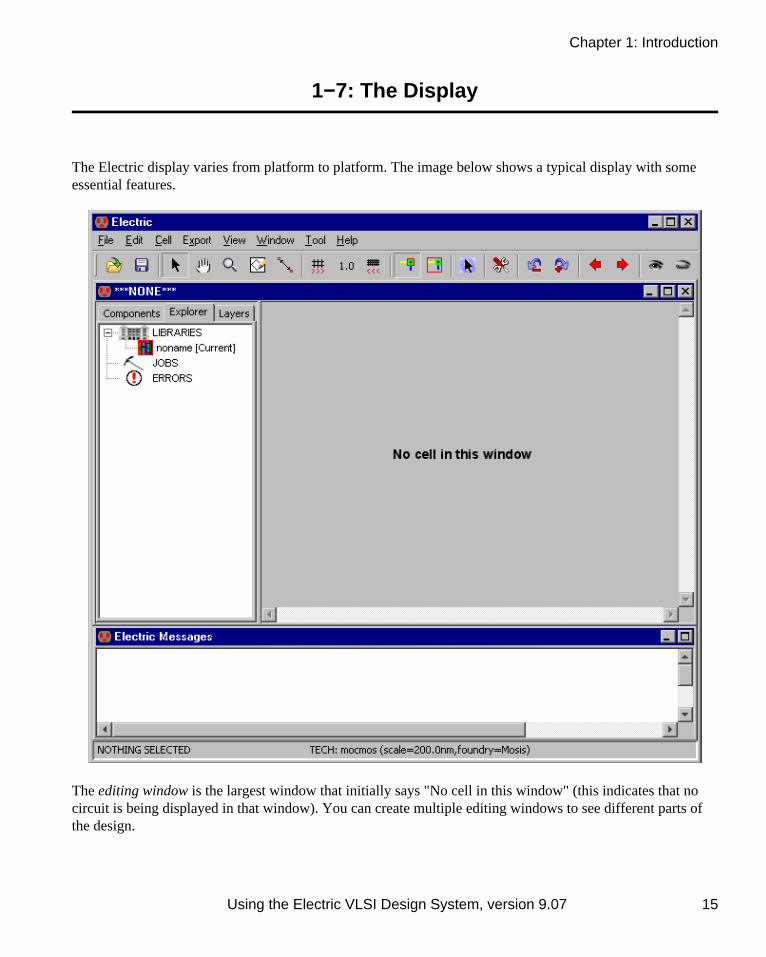
The Electric display varies from platform to platform. The image below shows a typical display with someessential features.
The editing window is the largest window that initially says "No cell in this window" (this indicates that nocircuit is being displayed in that window). You can create multiple editing windows to see different parts ofthe design.
Chapter 1: Introduction
Using the Electric VLSI Design System, version 9.07 15

The left side of the edit window is the sidebar that has 3 tabbed sections, the componentsmenu, the cell explorer, and the layers. You canmove it to the right side with the OnRight command (of menu Windows / Side Bar)and move it back with the On Left command.You can also request that the side bar always beon the right by checking "Side bar defaults to theright side" in the Display Control Preferences (inmenu File / Preferences..., "Display" section,"Display Control" tab).
The cell explorer lets you examine the hierarchy,system activity, and error messages (see Section4−5−2 for more).
The components menu shows a list of nodes(blue border) and arcs (red border) that can beused in design. The arrangement of the entries inthe components menu varies with the differenttechnologies. For MOS technologies, see Section7−4−2; for schematics, see Section 7−5−1; andfor artwork, see Section 7−6−1.
The top three entries in the components menu letyou place pure−layer nodes (see Section6−10−1), miscellaneous objects (see Section7−6−3) and instances of cells (see Section 3−3).
The layers tab lets you control which parts of thedisplay are visible. See Section 4−5−3 for moreon layer visibility.
Below the edit window is the messages window, which is used for all textual communication.
Above the edit windows is a pulldown menu along the top with command options. On some operatingsystems, the pulldown menu is part of the edit window, and on others it is separate. Below the pulldownmenu is a tool bar which has buttons for common functions.
Finally, the status area gives useful information about the design state. It appears along the bottom of theediting window or (in this example) at the bottom of the screen. The status area shows cursor coordinates,and can show global coordinates when traversing the hierarchy (see Section 4−3).
Chapter 1: Introduction
16 Using the Electric VLSI Design System, version 9.07

1−8: The Mouse
Electric mostly uses the left and right mouse buttons, although there are functions that can use a middlebutton. On Macintosh systems with only one button, hold the Command key to get the right button functions.
Modifier Button Action
Left Click Select
SHIFT Left Click Invert selection
CTRL Left Click Cycle through selected objects
CTRL + SHIFT Left Click Cycle through objects to Invert
Left Double Click Get Info
Left Drag Move selected objects or Select area
CTRL Left Drag Move selected objects, constrained
Right Click Draw or Connect Wire
CTRL Right Click Draw Wire (no connect)
SHIFT Right Click Zoom Out
SHIFT Right Drag Zoom In
CTRL + SHIFT Right Drag Draw Box
Middle Drag Pan Screen
SHIFT Middle Drag Select area without moving
Wheel Up/Down Scroll Up/Down
SHIFT Wheel Up/Down Scroll Right/Left
CTRL Wheel Up/Down Zoom in/out
By combining special keystrokes with the mouse functions, advanced layout operations can be done:
Switch Wiring Targets Hit Space while holding the Right mouse button to switch between possiblewiring targets under the mouse.
•
Switch Layers Type a number between 1−9 to switch layout layers. You can also use "+" and "−" tomove up or down by one layer (when typing "+", it is not necessary to hold the Shift key, so you arereally typing "=" on most keyboards). Additionally, if you have a port highlighted that can connect tothe new layer, a contact cut will be created at that point and connected to the port.
•
Abort Type ESCAPE to abort the current operation.•
Chapter 1: Introduction
Using the Electric VLSI Design System, version 9.07 17

1−9: The Keyboard
Many common commands can be invoked by typing "quick keys" for them. These quick keys are shown inthe pulldown menus next to the item. For example, the New Cell... command (in menu Cell) has the quickkey "Control−N". On the Macintosh, the menu shows "N", indicating that you must hold the command keywhile typing the "N"; on Windows and UNIX systems, the menu shows "Ctrl−N", indicating that you musthold the Control key while typing "N". There are also unshifted quick keys (for example, the letter "n" runsthe Place Cell Instance command).
To change the bindingsof quick keys, use theKey BindingsPreferences (in menuFile / Preferences...,"General" section, "KeyBindings" tab).
The dialog shows thehierarchical structure ofthe pulldown menus onthe top, and lets you addor remove key bindingsin the bottom area.
You can remove a quick key binding with the "Remove" button, and you can add a quick key binding withthe "Add" button. Change key bindings with caution, because it customizes your user interface, making itmore difficult for other users to work at your computer.
You can get to EVERY menu command with key mnemonics. The mnemonic keys are underlined in themenus. For example, the File menu has the "F" underlined, and the Print... command of that menu has the"P" underlined. This means that you can hold the Alt key and type "FP" to issue the print command. Notethat the mnemonic keys are different than the quick keys.
Chapter 1: Introduction
18 Using the Electric VLSI Design System, version 9.07

The default key bindings are shown here (use the Show Key Bindings command in menu Help to see thecurrent set). For alternate key binding sets that mimic Cadence, see Section 4−6−2.
Letter Control Plain Other
A Select All (see 2−1−1) Add Signal to Waveform (4−11)
B Size Interactively (2−5−1)
C Copy (6−1) Change (6−6)
D Down Hierarchy (3−5) Down Hierarchy In−place (3−5)Shift: Down HierarchyIn−place to Obj (3−5)
E Create Export (3−6−1)
F Focus on Highlighted (4−4−1) Full Unit Movement (2−4−1)
G Toggle Grid (4−7−1) Set Signal Low (4−11)
H Half Unit Movement (2−4−1)
I Object Properties (2−4−2)
J Rotate 90 Counterclockwise (2−6)
K Show Network (6−9−1)
L Find Text (4−9)
M Duplicate (6−1) Measure Mode (4−7−4)
N New Cell (3−2) Place Cell Instance (3−3)
O Open Library (3−9−2) Overlay Signal in Waveform (4−11)
P Peek (3−4) Pan Mode (4−4−2)
Q Quit (1−11−8) Cycle through windows (4−3)
R Remove Signal from Waveform (4−11)
S Save All Libraries (3−9−3) Select Mode (2−1−1)
T Toggle Negation (5−4−2) Place Annotation Text (2−2−1)
U Up Hierarchy (3−5) Select Object Under Cursor (2−1)
V Paste (6−1) Set Signal High (4−11)
W Close Window (4−3)
X Cut (6−1) Set Signal undefined (4−11)
Y Redo (6−7) Outline Edit Mode (6−10−2)
Z Undo (6−7) Zoom Mode (4−4−1)
Chapter 1: Introduction
Using the Electric VLSI Design System, version 9.07 19

Key Control Plain Shift Other
0 Zoom Out (4−4−1) Wire to Poly (1−8) See All Layers (4−5−3)
1 Wire to Metal−1 (1−8) See Metal−1 (4−5−3)F1: Mimic Stitch(9−6−3)
2 Pan Down (4−4−2) Wire to Metal−2 (1−8) See Metal−2/1 (4−5−3)F2: Auto Stitch(9−6−2)
3 Wire to Metal−3 (1−8) See Metal−3/2 (4−5−3)
4 Pan Left (4−4−2) Wire to Metal−4 (1−8) See Metal−4/3 (4−5−3)
5 Center cursor (4−4−2) Wire to Metal−5 (1−8) See Metal−5/4 (4−5−3)F5: Run DRC(9−2−1)
6 Pan Right (4−4−2) Wire to Metal−6 (1−8) See Metal−6/5 (4−5−3) F6: Array (6−4)
7 Zoom In (4−4−1) Wire to Metal−7 (1−8) See Metal−7/6 (4−5−3)F7: Repeat LastAction (6−7)
8 Pan Up (4−4−2) Wire to Metal−8 (1−8) See Metal−8/7 (4−5−3)
9 Fill Window (4−4−1) Wire to Metal−9 (1−8) See Metal−9/8 (4−5−3)F9: Tile WindowsVertically (4−3)
=Increase all Text Size(6−8−4)
Wire to next layer up(1−8)
−Decrease all Text Size(6−8−4)
Wire to next layerdown (1−8)
DEL Erase (2−3)
> Next Error (9−1)
< Previous Error (9−1)
]Next Error, sameWindow (9−1)
[Previous Error, sameWindow (9−1)
SpaceSwitch Wiring Target(1−8)
L arrow Move more left (2−4−1) Move left (2−4−1) Move more left (2−4−1)
R arrow Move more right (2−4−1)Move right (2−4−1) Move more right (2−4−1)
U arrow Move more up (2−4−1) Move up (2−4−1) Move more up (2−4−1)
D arrowMove more down(2−4−1)
Move down (2−4−1) Move more down (2−4−1)
Chapter 1: Introduction
20 Using the Electric VLSI Design System, version 9.07

1−10: IC Layout Tutorial
1−10−1: IC Layout Tutorial: Make a Cell
This section takes you through the design of some simple IC layout.
Before you can place any IC layout,the editing window must have a cellin it. Use the New Cell... command(in menu Cell). This will show adialog that lets you type a new cellname. Type the name ("MyCircuit"is used here) and click OK. Theediting window will no longer havethe "No cell in this window"message, and circuitry may now becreated.
After creating a cell, look at the cell explorer (inthe status bar on the left side of the edit window).Under the "LIBRARIES" icon, you will see thelist of libraries (currently only one called"noname"). If you open that library's icon, youwill see the cells in the library (currently only"MyCircuit").
1−10−2: IC Layout Tutorial: Create a Node
Layout is placed by selecting nodes from the side bar's components menu, and then wiring them together.This example shows two nodes that have been created. This was done by clicking on the appropriatecomponent menu entry, and then clicking again in the editing window to place that node. After clicking onthe component menu entry, the cursor changes to a pointing hand to indicate that you must select a locationfor the node. When placing the node, if you press the button and do not release it, you will see an outline ofthe new node, which you can drag to its proper location before releasing the button.
Chapter 1: Introduction
Using the Electric VLSI Design System, version 9.07 21

In this example, the top node is calledMetal−1−Polysilicon−1−Con (a contact betweenmetal layer 1 and polysilicon layer 1, found in thefifth entry from the bottom in the right column ofthe component menu). The node on the bottom iscalled N−Transistor (lower−right entry of thecomponent menu). Both of these nodes are from theMOSIS CMOS technology (which is listed as"mocmos" in the status area).
1−10−3: IC Layout Tutorial: Highlighting
A highlighted node has two selected areas: the nodeand a port on that node. Note that the transistor ishighlighted in the previous example, and the contactis highlighted in the example here. The largerselected area covers the node, and it surrounds the"important" part (for example, on the Transistor, itcovers only the overlap area, excluding the tabs ofactive and gate on the four sides). The smallerselected area is the currently highlighted port (thereare four possible ports on the transistor, but only oneon the contact).
To highlight a node, use the left button. The node, and the closest port to the cursor, will be selected. Afterhighlighting, you can hold the mouse button down and drag the highlighted object to a new location. Ifnothing is under the cursor when the selection button is pushed, you may drag the cursor while the buttonremains down to define an area in which all objects will be selected.
Another way to affect what is highlighted is to use the shift−left button. This button causes objecthighlighting to be reversed (highlighted objects become unhighlighted and unhighlighted objects arehighlighted).
The shape of the highlighted port is important. Ports are the sites of arc connections, so the end point of thearc must fall inside this port area. Ports may be rectangles, lines, single points (displayed as a "+"), or anyarbitrary shape. For example, when the active tabs of a transistor are highlighted, the port is shown as a line.
Chapter 1: Introduction
22 Using the Electric VLSI Design System, version 9.07

1−10−4: IC Layout Tutorial: Make an Arc
To wire a component, select it, movethe cursor away from the component,and use the right button. A wire will becreated that runs from the componentto the location of the cursor. Note thatthe wire is a fixed−angle wire whichmeans that it will be drawn along ahorizontal or vertical path from theoriginating node.
To see where the wire will end, click but do not release the button and drag the outline of the wire'sterminating node (a pin) until it is in the proper location. It is highly recommended that you do all wiringoperations this way, because wiring is quite complex and can follow many different paths.
Once a wire has been created, the other end is highlighted (see above). This is the highlighting of a pin nodethat was created to hold the other end of the arc. Because it is a node, the right button can be used again tocontinue the wire to a new location. If, during wiring, the cursor is dragged on top of an existing component,the wire will attach to that component.
To remove wires or components, you can issue the Undo command (in menu Edit) to remove the last createdobject. Alternatively, you can select the component and use the Selected command (in menu Edit / Erase).
1−10−5: IC Layout Tutorial: Constraints
Once components are wired, moving them will also move their connecting wires. Notice that the wiresstretch and move to maintain the connections. What actually happens is that the programmable constraintsystem follows instructions stored on the wires, and reacts to node changes. The default wire isfixed−angle and slidable, so the letters "FS" are shown when the wire is highlighted.
Select a wire and issue the Rigid command (in menu Edit / Arc). The letters change to "R" on the arc andthe wire no longer stretches when nodes move. Find another arc and issue the Not Fixed−angle command.Now observe the effects of an unconstrained arc as its neighboring nodes move. These arc constraints can bereversed with the Rigid and Fixed−angle commands. See Section 5−2−1 for more on these constraints.
Chapter 1: Introduction
Using the Electric VLSI Design System, version 9.07 23

1−10−6: IC Layout Tutorial: Adding Contacts to a Transistor
One very common structure in IC layout is the transistor−contact combination. Here you will see the properway to construct it.
Start with a transistor (inthis example on the left, ann−transistor).
•
Rotate the transistor so thatthe gate is vertical. To dothis, use the 90 DegreeCounterclockwise command(in menu Edit / Rotate), orjust type Control−J.
•
Note that the active gate onthe left is highlighted (it isjust a line).
•
Although the default transistor is 2x3 in size, most people want them to be wider. For the purposes of thisexample, make the transistor be 12 wide. To do this, select the node and use the Object Properties command(in menu Edit / Properties).
Two easierways to see theobjectsproperties areto double−clickon the node, orselect it andtype Control−I.When the"nodeProperties"dialog appears,make the width12 and clickOK.
Chapter 1: Introduction
24 Using the Electric VLSI Design System, version 9.07

Next we need a contact. Choose a"Metal−1−N−Active−Con" toconnect the N−Active to Metal−1.Make its size be 5x12 instead ofthe default 5x5. Notice thatcontacts are "smart" about the cuts,and add them to fill the node. Notealso that the port (the innerrectangle) grows with the node.
Designers who have used polygon−based systems will be tempted to move these two nodes together so thatthey form the desired structure:
THIS IS WRONG!
Electric is a connectivity−oriented system,and insists that these components be wiredtogether.
The easiest way to connect the contact to the transistor is to spread the nodes apart, wire them, and then pushthem back together. These two figures show the transistor and contact nodes, spread apart, and connected byan arc.
Chapter 1: Introduction
Using the Electric VLSI Design System, version 9.07 25

On the left, the nodes and their ports; on the right, the arc.
The arc was made by selecting one node, clicking and HOLDING the right button, dragging the mouse overthe other component, and then releasing the button to create the arc.
Notice that the ends of an arc are centered and indented from the edge by half of the arc's width (the ends areillustrated by "+" on the right). The ends of an arc must sit inside of the ports. If an arc moves such that itsends are still in the ports, then the nodes don't have to move. See Section 5−4−3 for more on arc geometry.
THIS IS RIGHT!
Now that the nodes are wired together,bring the contact in close. Notice that thearc has shrunk down to a square, with theendpoints very close together. If you makethe arc rigid, the two nodes will be heldtogether in this configuration. To do this,use the Rigid command (in menu Edit /Arc). As shown here, the "R" on theselected arc tells you that it has been maderigid. See Section 5−2−1 for more arcconstraints.
Chapter 1: Introduction
26 Using the Electric VLSI Design System, version 9.07

Another common situation in making contacts meet transistors is when the sizes are not the same. In thisexample, the contact is the default size. The arc runs from the center of the contact's port to the top of thetransistor's port. The finished layout is shown on the right.
Here are some points about connecting nodes with arcs:
By doing it, the system understands your circuit connectivity and uses it in many other places.• The design−rule checker will flag objects that touch but are not connected.• After you create one of these structures, it can be copied−and−pasted many times. Use the Copy andPaste commands (in menu Edit). Note that when pasting, you must not have anything selected, orelse it tries to replace the selected objects with the copied objects. Therefore, to duplicate somecircuitry, select it, Copy, click away to deselect, and then Paste.
•
If you want to rotate or mirror these structures, select all of it (both nodes and the arc) and use theRotate or Mirror commands (in menu Edit).
•
Chapter 1: Introduction
Using the Electric VLSI Design System, version 9.07 27

1−10−7: IC Layout Tutorial: Hierarchy
Electric supports hierarchy byallowing you to place instances ofanother cell. These instances arenodes, just like the simpler ones inthe component menu. To seehierarchy in action, create a new cellwith the New Cell... command (inmenu Cell). Make sure the "Makenew window" option is checked inthe dialog. Then type the new cellname ("Higher" is used in theexample here).
A new (empty) cell will appear in a separate window. Try creating a few simple nodes in this new window(place a contact or two).
Now place an instance of the othercell by using the Place CellInstance... command (in menu Cell).You can also click the "Cell" entry inthe component menu. You will begiven a list of cells to create: selectthe one that is in the OTHER window(the one called "MyCircuit" in thisexample). Then click in the newercell to create the instance.
Chapter 1: Introduction
28 Using the Electric VLSI Design System, version 9.07

The box that appears is a node in the same sense
as the contacts and transistors: it can be moved,wired, and so on. In addition, because the nodecontains subcomponents, you can see itscontents by selecting it and using the One LevelDown command (in menu Cell / Expand CellInstances, or click on the opened−eye button inthe tool bar). Note that if the objects in a cell nolonger fit in the display window, use the FillDisplay command (in menu Window).
1−10−8: IC Layout Tutorial: Exports
Before you can attach wires to the instance node, there must be connection sites, or ports on that node.Primitive nodes such as contacts and transistors already have their ports established, but you must explicitlycreate ports for cell instances. This is done by creating exports inside the cell definition.
Move the cursor to the windowwith the lower−level cell("MyCircuit") and select thecontact node. Then issue theCreate Export... command (inmenu Export). You will beprompted for an export name andits characteristic (thecharacteristics can be ignored fornow).
This takes the port onthe contact node andexports it to the outsideworld. Its name will bevisible on theunexpanded instancenode in thehigher−level cell. Youcan now connect wiresto that node in just thesame way as you wiredthe contact.
Chapter 1: Introduction
Using the Electric VLSI Design System, version 9.07 29

1−11: Schematics Tutorial
1−11−1: Schematics Tutorial: Make a Cell
This section takes you through the design of some simple schematics.
Before you can place anyschematics, the editing window musthave a cell in it. Use the NewCell... command (in menu Cell).Type the name ("MyCircuit" is usedhere) and select the "schematic"view.
The editing window will no longer have the "No cell in this window" message, and circuitry may now becreated. Note that the component menu on the left will change to show schematics primitives. Also, theSchematic technology is now listed in the status area at the bottom of the screen.
After creating a cell, look at the cell explorer (inthe status bar on the left side of the edit window).In the "LIBRARIES" icon, you will see the listof libraries (currently only one called "noname").If you open that library's icon, you will see thecells in the library (currently only "MyCircuit").
Chapter 1: Introduction
30 Using the Electric VLSI Design System, version 9.07

1−11−2: Schematics Tutorial: Make a Node
Schematic nodes are placed by selectingthem from the side bar's components menu(on the left), and then wiring them together.This example shows two nodes that havebeen created. This was done by clicking onthe appropriate component menu entry, andthen clicking again in the editing window toplace that node.
After clicking on the component menu entry, the cursor changes to a pointing hand to indicate that you mustselect a location for the node. When placing the node, if you press the button and do not release it, you willsee an outline of the new node, which you can drag to its proper location before releasing the button.
In this example, the top node is called a Buffer (found on the right side of the component menu in the thirdentry from the top). The node on the bottom is called an And (top entry on the right).
1−11−3: Schematics Tutorial: Highlighting
A highlighted node has two selected parts: thenode and a port on that node. Note that theAnd is highlighted in the previous example,and the Buffer is highlighted in the examplehere. The little "+" sign is the currentlyhighlighted port (there are two possible portson these nodes, on the input and the output).
To highlight a node, use the left button. The node, and the closest port to the cursor, will be selected. Afterhighlighting, you can hold the mouse button down and drag the highlighted object to a new location. Ifnothing is under the cursor when the selection button is pushed, you may drag the cursor while the buttonremains down to define an area in which all objects will be selected.
Another way to affect what is highlighted is to use the shift−left button. This button causes objecthighlighting to be reversed (highlighted objects become unhighlighted and unhighlighted objects arehighlighted).
The shape of the highlighted port is important. Ports are the sites of arc connections, so the end point of thearc must fall inside this port area. Ports may be rectangles, lines, single points (displayed as a "+"), or anyarbitrary shape. For example, the entire left side of the And gate is the input port and so its highlighting is aline.
Chapter 1: Introduction
Using the Electric VLSI Design System, version 9.07 31

1−11−4: Schematics Tutorial: Make an Arc
To wire a component, select it, move thecursor away from the component, and use theright button. If you click the right button andhold it without releasing, then you can movearound and see where the wire will go whenyou do release.
A wire will be created that runs from the component to the location of the cursor. Note that the wire is afixed−angle wire which means that it will be drawn along a horizontal, vertical, or 45−degree path from theoriginating node. To see where the wire will end, click but do not release the button and drag the outline ofthe wire's terminating node (a pin) until it is in the proper location. It is highly recommended that you do allwiring operations this way, because wiring is quite complex and can follow many different paths.
Once a wire has been created, the other end is highlighted (see above). This is the highlighting of a pin nodethat was created to hold the other end of the arc. Because it is a node, the right button can be used again tocontinue the wire to a new location. If, while wiring, the dragged location is over an existing component, thewire will attach to that component.
To remove wires or nodes, you can issue the Undo command (in menu Edit) to remove the last createdobject. Alternatively, you can select the component and use the Selected command (in menu Edit / Erase).
1−11−5: Schematics Tutorial: Multi−Input gates and Negation
One aspect of the And, Or, and Xor gates that you will notice is that their left side (the input side) can acceptany number of wires. To see this in action, place one of these components in the cell. Then repeatedly selectits left side and use the right button to draw wires out of it. Each wire will connect at a different location inthe input port, and once the side fills with arcs, it will automatically grow to fit more. Note that the verticalcursor location along the input side is used to select the position that will be used when a new wire is added.
To negate an input or output of a digital gate, select the port or the arc anduse the Toggle Port Negation command (in menu Edit / TechnologySpecific). With this facility, you can construct arbitrary gate configurations.
Chapter 1: Introduction
32 Using the Electric VLSI Design System, version 9.07

1−11−6: Schematics Tutorial: Constraints
Once components are wired, moving them will also move their connecting wires. Notice that the wiresstretch and move to maintain the connections. What actually happens is that the programmable constraintsystem follows instructions stored on the wires, and reacts to component changes. The default wire isfixed−angle, so the letter "F" is shown when the wire is highlighted.
Select a wire and issue the Rigid command (in menu Edit / Arc). The letter changes to "R" on the arc andthe wire no longer stretches when components move. Find another arc and issue the NotFixed−angle command. Now observe the effects of an unconstrained arc as its neighboring nodes move.These arc constraints can be reversed with the Rigid and Fixed−angle commands. See Section 5−2−1 formore on these constraints.
1−11−7: Schematics Tutorial: Hierarchy and Icons
Electric supports hierarchy by allowing you to create icons for a schematic and place them in another cell.Before creating an icon, all connection points to the schematic should be defined. To define connectionpoints for a schematic, you must create exports on the schematic.
To see an example of this, selectthe output port of the Buffer nodeand issue the CreateExport... command (in menuExport). You will be promptedfor an export name and itscharacteristics (set thecharacteristics to "output").
The output port on the buffer node is now exported to theoutside world. Run a wire from the input side of the And nodeand export the pin at the end of the wire. Your circuit shouldlook like this.
Chapter 1: Introduction
Using the Electric VLSI Design System, version 9.07 33

You can now make an icon for thiscircuit by using the MakeIcon command (in menu View). Theicon will be placed in your circuit (youmay have to move it away from the restof the circuitry). The result will look likethis.
To test this icon in a circuit, create anew cell in which to place instancesof the icon. Use the NewCell... command (in menu Cell).Type the new cell name ("Higher" isused in the example here) and makesure its view is "schematic".
A new (empty) cell will appear in aseparate window. Try creating a fewsimple nodes in this new window(place a gate or two).
Now place an instance of the othercell by using the Place CellInstance... command (in menu Cell).You can also click the "Cell" entry inthe component menu. You will begiven a list of cells to create: selectthe one that is in the OTHER window(the one called "MyCircuit{ic}" inthis example). Then click in thenewer cell to create the instance.
Chapter 1: Introduction
34 Using the Electric VLSI Design System, version 9.07

The icon that appears is a node in the same sense as theBuffer and And gate: it can be moved, wired, and so on.In addition, because the node contains subcomponents,you can see its contents by selecting it and using theDown Hierarchy command (in menu Cell / DownHierarchy). Note that if the objects in a cell no longer fitin the display window, use the Fill Window command(in menu Window).
1−11−8: Schematics Tutorial: Final Points
Some final commands that should be mentioned in this introductory example are the Save Library and theQuit commands which can be found in the File menu. They do the obvious things.
Chapter 1: Introduction
Using the Electric VLSI Design System, version 9.07 35

1−12: Schematics and Layout Tutorial
1−12−1: Introduction to Schematic/Layout Tutorial
This tutorial was originally written by David Harris at Harvey Mudd College as the first in a set of labinstructions for an undergraduate−level CMOS VLSI design class. It provides very basic instructions toacclimatize first−time users with Electric. As such, it is not a full introduction to using Electric, nor does itcover many commonly used commands.
What this tutorial does cover is:
Basic schematic editing. You will create a simple "nand" gate.• Layout drawing. You will create the IC layout of the "nand" gate.• Hierarchy. You will assemble the "nand" with an "inverter" to build an "and" gate.• Analysis. You will run the design rule checker on the layout, and will compare the layout with theschematic.
•
To begin, load the "mipscells" library from the Static Free Software website(www.staticfreesoft.com/productsLibraries.html). This library contains many parts of the MIPS processorthat are provided to you. You will add your new design to the library as you work through the tutorial.
1−12−2: Schematic Entry
Your first task is to create a schematic for a 2−input NAND gate. Each design is kept in a cell; for example,your schematic will be in the "nand2{sch}" cell, while your layout will eventually go in the "nand2{lay}"cell and your AND gate will go in the "and2{sch}" cell. Use the New Cell command (in menu Cell), or justtype Ctrl−N. Enter "nand2" as the cell name and select "schematic" as the view. The editing window willnow have the title "mipscells:nand2{sch}" indicating the library, cell name, and view. It is useful to put alabel inside a cell, in addition to assigning its given name. To label your cell, select the "Components" tab ofthe sidebar (on the left), click on "Misc.", and select "Annotation text". Move the cursor to the location whereyou want the label to appear, and click to create the text. Change the text by double−clicking on it and typing"nand2". When done typing, click away from the text to exit the in−place editing (the text is now selectedwith an "X" through it). Then bring up the full properties dialog for this text with the ObjectProperties command (in menu Edit / Properties), or just type Ctrl−I. Set the "Text Size" to 5 units and clickOK. When your cell is finished, you can move this label to a sensible location.
Electric defines various technologies for schematics and layout. To draw transistor−level schematics, you canuse the symbols in the Components tab of the side bar.
Chapter 1: Introduction
36 Using the Electric VLSI Design System, version 9.07

Your goal is to draw a gate like theone shown here. Turn on the grid tohelp you align objects. To do this, usethe Toggle Grid command (in menuWindow), or just type Ctrl−G. Clickon an nMOS transistor symbol in theComponents tab on the left side of thescreen. Then click in your schematicwindow to place the transistor in thecircuit (perform this as two separateclicks, not drag−and−drop). Repeatuntil you have two nMOS transistors,two pMOS transistors, the Powersymbol, and the Ground symbolarranged on the page.
These symbols are nodes in Electric parlance. You may move the nodes around by clicking and dragging.The transistors default to a width/length value of 2/2. Double−click on the pMOS transistor and change itswidth to 12. Recall that nMOS transistors are roughly twice as strong as pMOS transistors. So a single nMOStransistor would only have to be 6 wide. However, because the nMOS transistors are in series, they shouldalso be 12 wide.
Now, connect the nodes with wires (called arcs in Electric parlance). Notice that when you click on a node,the closest port is also selected. These ports are the sides of arc connections. Click on a port such as the gate,source, or drain of a transistor. Right−click, hold the mouse, and drag away from the node. When you releasethe mouse, an arc will be created from the original node to the location of the cursor. A new "pin" node willalso be created at the cursor to hold the other end of the arc. If you right−click and drag over an existingnode, then you will connect to it. If two objects to be connected are not lined up, Electric will create two arcsto join them. The location of the cursor determines the angle of the bend, so wiggle it to see how the two arcswill run before releasing the button and creating the connection. See Section 2−2−2 for more on arc creation.
When the schematic is wired, you will need to create exports which define inputs and outputs of the cell.From the Components tab, select the "Off−Page" symbol and place it in the circuit. Connect the tip of thearrow the proper place in the circuit. To make an export on the other side of the Off−Page, select that portand use the Create Export command (in menu Export), or just type Ctrl−E. Name the export "a" and defineits characteristic as "input". Similarly, create Off−Page symbols and exports for "b" and "y".
Now is a good time to save your library. Use the Save Library command (in menu File), or just type Ctrl−S.Get into the habit of saving your library regularly. Also, learn the keyboard shortcuts for the commands youuse frequently.
Chapter 1: Introduction
Using the Electric VLSI Design System, version 9.07 37
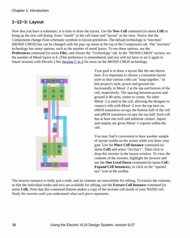
1−12−3: Layout
Now that you have a schematic, it is time to draw the layout. Use the New Cell command (in menu Cell) tobring up the new cell dialog. Enter "nand2" as the cell name and "layout" as the view. Notice that theComponents change from schematic symbols to layout primitives. The default technology is "mocmos"(MOSIS CMOS) but can be changed with the pop−up menu at the top of the Components tab. The "mocmos"technology has many options, such as the number of metal layers. To see these options, use thePreferences command (in menu File), and choose the "Technology" tab. In the "MOSIS CMOS" section, setthe number of Metal layers to 6. (This preference is remembered, and you will not have to set it again infuture sessions with Electric.) See Section 7−4−2 for more on the MOSIS CMOS technology.
Your goal is to draw a layout like the one shownhere. It is important to choose a consistent layoutstyle so that various cells can "snap together." Inthis project's style, power and ground runhorizontally in Metal−2 at the top and bottom of thecell, respectively. The spacing between power andground is 80 units, center to center. No otherMetal−2 is used in the cell, allowing the designer toconnect cells with Metal−2 over the top later on.nMOS transistors occupy the bottom half of the celland pMOS transistors occupy the top half. Each cellhas at least one well and substrate contact. Inputsand outputs are given Metal−1 exports within thecell.
You may find it convenient to have another sampleof layout visible on the screen while you draw yourgate. Use the Place Cell Instance command (inmenu Cell) and select "inv{lay}". Then click todrop this inverter in the layout window. To view thecontents of the inverter, highlight the inverter anduse the One Level Down command (in menu Cell /Expand Cell Instances), or click on the "openedeye" icon in the toolbar.
The inverter instance is really just a node, and its contents are unavailable for editing. To extract the contents,so that the individual nodes and arcs are available for editing, use the Extract Cell Instance command (inmenu Cell). Note that this command flattens makes a copy of the inverter cell inside of your NAND cell.Study the inverter until you understand what each piece represents.
Chapter 1: Introduction
38 Using the Electric VLSI Design System, version 9.07

Start by drawing your nMOStransistors. Recall that an nMOStransistor is formed when polysiliconcrosses N−diffusion. N−diffusion isrepresented in Electric as greendiffusion, surrounded by a dottedyellow N−select layer all within ahashed brown P−well background.This set of layers is convenientlyprovided as a 3−terminal transistornode in Electric. Move the mouse tothe Components tab on the left side ofthe screen.
As you move the mouse over various nodes, their name will appear in the status area at the bottom of thescreen. Click on the N−Transistor, and click again in the layout window to drop the transistor in place. Torotate the transistor so that the red polysilicon gate is oriented vertically, use the 90 DegreesCounterclockwise command (in menu Edit / Rotate), or just type Ctrl−J. There are two nMOS transistors inseries in a 2−input NAND gate, so we would like to make each wider to compensate. Double−click on thetransistor (or type Ctrl−I). In the node properties dialog, adjust the width to 12.
We need two transistors in series, so copy and paste the transistor you have drawn. You can also duplicatethe selected object with the Duplicate command (in menu Edit) or just type Ctrl−M. Drag the two transistorsalong side each other so they are not quite touching. Click the diffusion (source/drain) of one of thetransistors and right click on the diffusion of the other transistor to connect the two. Notice that Electric usesnodes and arcs in IC layout as well as in schematics. Once connected, drag the two transistors until thepolysilicon gates are 3 units apart, looking like they do below. You will probably find it helpful to turn on thegrid (type Ctrl−G). The grid defaults to small dots every unit and large dots every 10 units. You can changethis with the Preferences command (in menu File), "Display" section, "Grid" panel. Change the "Frequencyof bold dots" to 7, because the cells in this library have a wire pitch of seven.
You can move objects around with the arrow keys on the keyboard. The distance that they move defaults to 1unit, but this can be changed by using the "Make grid larger" or "Make grid smaller" icons in the toolbar (orby pressing the "f" or "h" keys). You will avoid messy problems by keeping your layout on a unit grid asmuch as possible. Inevitably, though, you will create structures that are an odd number of units in width andthus will have either centers or edges on a half−unit boundary. (To move an object 7 units per click, or theequivalent of one bold−spaced unit, press Control and then press the appropriate arrow key. If you first hit"h" and then the control−arrow key will move an item one−half the distance of a bold−spaced unit, 3.5 in thiscase.)
Electric has an interactive design rule checker (DRC). If you place elements too closely together, it willreport errors in the "Messages" window. Try dragging one of the transistors until its gate is only 2 units fromthe other. Observe the DRC error. Then drag the transistors back to proper spacing. When you are in doubtabout spacing, you can recheck the cell with the Check Hierarchically command (in menu Tools / DRC), orjust type the F5 key.
Chapter 1: Introduction
Using the Electric VLSI Design System, version 9.07 39

Next we will create the contacts from theN−diffusion to Metal−1. Diffusion is also referred toas "active". Drop a Metal−1−N−Active−Contactnode in the layout window and double−click tochange its Y size to 12. You will need a secondcontact for the other end of the series stack of nMOStransistors, so duplicate the contact you have drawn(type Ctrl−M). Move the contacts near each end ofthe transistor stack and draw diffusion lines toconnect to the transistors.
A quick way to connect many items that aretouching is to use the "auto router". To do this, selectall of the objects to be routed (click and drag aselection box over them) and use the Auto−StitchHighlighted Now command (in menu Tools /Routing), or just type the F2 key. See Section9−6−2 for more on auto−stitching.
Once the contacts are connected to the transistors you will need a gap of only 1 unit between the metal andpolysilicon. Use the design rule checker to ensure you are as close as possible but no closer. Using similarsteps, draw two pMOS transistors in parallel and create contacts from the P−diffusion to Metal−1. At thispoint, your layout should look something like this.
Draw wires to connect the polysilicon gates, forming inputs "a" and "b", and the Metal−1 output node "y".Then add Metal−2 power and ground lines. You can create these Metal−2 wires by creating a "Metal−2−Pin"node and right−clicking on it to draw a wire. Use the grid to make sure that the Metal−2 wires are 80 unitsapart. This is the same spacing as the power/ground lines of the inverter. Note that when two objects areselected, the Properties dialog box (Ctrl−I), also tells the distance between them.
A via, called "Metal−1−Metal−2−Con", is required to connect the Metal−1 to the Metal−2 lines. Select anactive contact and right−click to connect it to the ground line. Electric will automatically create the necessaryvia for you while making the connection. Complete the other connections to power and ground. Let powerand ground extend 2 units beyond the contents of the cell (excluding wells) on either side so that cells may"snap together" with their contents separated by 4 units (so design rules are satisfied).
Recall that well contacts are required to keep the diodes between the cells and source/drain diffusion reversebiased. We will place an N−well contact and a P−well contact in each cell. It is often easiest to drop the"Metal−1−N−Well−Con" near the desired destination (near VDD), then right click on the power line tocreate the via. Then drag the contact until it overlaps the via to form a stack of N+ diffusion, the diffusion toMetal−1 contact, Metal−1, the Metal−1−Metal−2−Con, and Metal−2. Repeat with the P−well.
In our datapath design style, we will be connecting gates, with horizontal and Metal−2 lines. Metal−2 cannotconnect directly to the polysilicon gates. Therefore, we will add contacts from the polysilicon gate inputs toMetal−1 to facilitate connections later in our design. Place a "Metal−1−Polysilicon−1−Con" node near the
Chapter 1: Introduction
40 Using the Electric VLSI Design System, version 9.07

left polysilicon gate. Connect it to the polysilicon gate and drag it near the gate. You will find a 3 unitseparation requirement from the Metal−1 in the contact to the metal forming the output "y". Add a short stripof Metal−1 near the contact to give yourself a landing pad for a via later in the design. You may find Electricwants to draw your strip from the contact in polysilicon rather than Metal−1. To tell Electric explicitly whichlayer you want, click over the Metal−1 arc in the Component tab (arcs have red borders). Then draw yourwire.
Electric is agnostic about the polarity of well and substrate; it generates both n− and p−well layers. In ourprocess that has a p−substrate already, the p−well, indicated by brown slanting lines, will be ignored. Then−well, indicated by small brown dots, will define the well on the chip. Electric only generates enough wellto surround the n and p diffusion regions of the chip. (Electric creates well contacts that are only 11 unitswide! This will generate a DRC error, but this behavior is intentional. Wells should be 12 units wide to meetDRC's expectations.) It is a good idea to create rectangles of well to entirely cover each cell so that when youabut multiple cells you don't end up with awkward gaps between wells that cause design rule errors. To dothis, click on the "Pure" entry of the Components tab and select "N−Well−Node" or "P−Well−Node". Tochange its size so that it entirely covers the existing well, resize it with the Interactively command (in menuEdit / Size) or just type Ctrl−B. You will find the pure layer nodes are annoying because you will tend toselect them when you really want to select a transistor or wire. To avoid this problem, select them and use theMake Selected Hard command (in menu Edit / Selection) to make the node hard−to−select. Once an item isdefined as hard−to−select, you must use "special select" mode to be able to select it (click on the arrow withthe letters "SP" in the toolbar). You can use the Make Selected Easy command if you want to restore a nodeor arc to be easily selected. Electric also provides the Coverage Implants Generator command (in menuTools / Generation) that automatically creates hard−to−select pure layer nodes for N and P wells. Thiscommand is convenient for simple geometries inside of a cell.
Create exports for the cell. When you use the cell in another design, the exports define the locations that youcan connect to the cell. Click near the end of the short Metal−1 input line that you just drew on the left gate,and select the Metal−1−Pin node. If you accidentally select the Metal−1 arc instead, click elsewhere in spaceto deselect the arc, then try again to find the pin. You may also try holding the Control key while clicking tocycle through everything that is under the cursor. Add an input export called "a" (type Ctrl−E to get theexport dialog). Repeat for input "b". Export output "y" from the metal line connecting the nMOS and pMOStransistors. You may have to place an extra pin and connect it to the output line to give yourself a pin toexport as "y". Also export "vdd" and "gnd" from the Metal−2 arcs; these should be of type power and ground,respectively. Electric recognizes "vdd" and "gnd" as special names, so be sure to use them.
Chapter 1: Introduction
Using the Electric VLSI Design System, version 9.07 41

1−12−4: Hierarchical Design
Now that you have a 2−input NAND gate, you can use it, and an inverter, to construct a 2−input AND gate.Such hierarchical design is very important in the creation of complex systems. You have found that thelayout of an individual cell can be quite time consuming. It is very helpful to reuse cells wherever possible toavoid unnecessary drawing. Moreover, hierarchical design makes fixing errors much easier. For example, ifyou had a chip with a thousand NAND gates and made an error in the NAND design, you would prefer tohave to fix only one NAND cell so that all thousand instances of it inherit the correction.
Each schematic has a corresponding symbol (an icon), used to represent the cell in a higher−level schematic.For example, open the "inv{sch}" and "inv{ic}" cells to see the inverter schematic and icon. You will need tocreate an icon for your 2−input NAND gate. When creating your icon, it is a good idea to keep everythingaligned to the 1 unit grid; this will make connecting icons simpler and cleaner when you use it in another cell.
Edit your "nand2{sch}" cell and use the MakeIcon View command (in menu View). Electricwill create a generic icon based on the exports asshown here. It will drop the icon in theschematic for handy reference; drag the iconaway from the transistors so it leaves theschematic readable.
A schematic is easier to read when familiaricons are used instead of generic boxes.Modify the icon to look like this. Pay attentionto the dimensions of the icon; the overalldesign will look more readable if icons are ofconsistent sizes.
To edit the icon, click on it and use the Down Hierarchy command (in menu Cell / Down Hierarchy) orjust type Ctrl−D. The Component tab will now show with various shapes (this is the "Artwork" technology).Delete the generic black box but leave the input and output wires. Turn on the grid.
The body of the NAND is formed from an open C−shaped polygon, a semicircle, and a small negating circle.To form the semicircle, create an unfilled circle node. Double−click to change its size to 6x6 and to span only180 degrees of the circle. Use the rotate commands under the Edit menu to rotate the semicircle into place.Place another circle, adjust its size to 1x1, and move it into place. Alternatively, you can type "h" and use thearrow keys to move objects by 1/2 grid increments, then press "f" to return to full grid movement.
Chapter 1: Introduction
42 Using the Electric VLSI Design System, version 9.07

The Opened−Polygon node can be used to form theC−shaped body. When first created, it appears as azigzag, shown here. To manipulate its shape, select it andenter "outline edit mode" by using the Toggle OutlineEdit command (in menu Edit / Modes / Edit), or justtype "y", or click on the icon in the toolbar.
In this mode, you can use the left button to select and move points and the right button to create points. Sincethe default Opened−Polygon node has 4 points already, you should be able to form the "C" shape simply byclicking and dragging these points. Outline edit mode is not entirely intuitive at first, but you will master itwith practice. When done, use the same command to exit the mode (just type "y"). See Section 6−10−1 formore on outline editing.
Electric is finicky about moving the lines with inputs or outputs. If you click and drag to select the line alongwith the input, everything moves as expected. If you try to move only the export name, it won’t move as youmight expect. Therefore, make a habit of moving both the line and export simultaneously when editing icons.For appearance, remove the thin export connector lines. Replace these with bold black lines. You can easilydo this by left clicking on a wire of the icon, then right−clicking, placing the cursor where you want the endpoint of the wire to be. Electric draws a wire that extends from the artwork of the icon.
Use the "Text" item in theComponent menu to place alabel "nand2" in the icon.Make the text be 2 unitshigh.
Now that you have an icon with three exports, create a new schematic called "and2" (don't forget to set theview to "schematic"). Use the Place Cell Instance command (in menu Edit) to instantiate a "nand2{ic}" andan "inv{ic}". Wire the two together and create exports on inputs "a" and "b" and output "y". Double−click onthe wire between the two gates and give it a name like "yb" so you know what you are looking at insimulation. It is good practice to label every net in a design. When you are done, your "and2" schematicshould look like this.
Next, create a new layout called "and2" (remember to select the "layout" view). Instantiate the "nand2{lay}"and "inv{lay}" layouts. ALWAYS use the Place Cell Instance command to create layout from pre−existingcells. NEVER build a cell by cutting and pasting entire existing cells. If you do, then make a correction to theoriginal cell, your correction will not propagate to the new layout.
Chapter 1: Introduction
Using the Electric VLSI Design System, version 9.07 43

Initially the cell instances appear as blackboxes with ports. Select both instances anduse the All the Way command (in menuCell / Expand Cell Instances) to view thecontents of each layout. Wire power andground to each other. Move the cellstogether as closely as possible withoutviolating design rules. You may need toplace large blobs of pure layer nodes overthe n−well and p−well to avoidintroducing well−related errors fromnotches in the wells. Connect the output ofthe "nand2" to the input of the "inv" usingMetal−1. Remember that connections mayonly occur between the ports of the twocells. Also connect the power and groundlines of the cells using Metal−2. Exportthe two inputs, the output, and power andground. An easy way to do this is to usethe Re−Export Everything command (inmenu Exports) to bring exports to thesurface level.
The Messages window shows how many ports were exported. The final gate should resemble this.
1−12−5: Analysis
Design Rule Checking
At any time, you can check your layout against the design rules by using the CheckHierarchically command (in menu Tools / DRC), or just type the F5 key. When DRC is done, use the ">"key to step through and highlight errors; see the Messages window for comments.
You can also use this command to check a schematic. Schematic design rules are simply "rules of etiquette"which report unusual situations in the circuit. See Section 9−2−1 for more on DRC.
Network Consistency Checking
One of the most useful analysis tools is Network Consistency Checking (NCC). This compares the networksin two different cells to make sure they are equivalent (this step is sometimes called LVS:layout−versus−schematic).
To run NCC, edit either the layout or the schematic cell, and use the Schematic and Layout Views of Cellin Current Window command (in menu Tools / NCC). This check will not consider transistor sizes, only
Chapter 1: Introduction
44 Using the Electric VLSI Design System, version 9.07

circuit connectivity.
When the circuit has passed NCC at the connectivity level, turn on transistor size checking. To do this, check"Check transistor sizes" in the NCC Preferences (use the Preferences command in menu File, section"Tools", tab "NCC").
Electric ideally likes layout, schematic and icons of the same items to be named identically (i.e."nand2{sch}" and "nand2{lay}" have identical names). Having the same name places cells in the same cellgroup. (Much of this naming happens automatically in Electric when new views of a current cell are made.)If the two cells to be compared are not in the same group, additional work is needed to tell NCC what tocompare. See Section 9−7−1 for more on NCC.
Simulation
Electric has two built−in simulators, and can interface to many more. The built−in simulators are ALS andIRSIM. ALS is a logic−level simulator, and is not useful for transistor−level design. IRSIM is a gate−levelsimulator, and can handle the transistors in this example. Unfortunately, IRSIM is not packaged with thebasic Electric system (it is a free, but separate, "plugin"). See Section 1−5 for details on adding the IRSIMsimulator to Electric.
To simulate a circuit with IRSIM, use the IRSIM: Simulate Current Cell command (in menu Tools /Simulation (Built−in)). A waveform window appears to show the simulation status. To get the waveformwindow and your schematic/layout to appear side−by−side, use the Tile Vertically command (in menuWindow / Adjust Position).
The exported signals of your design will automatically appear in the waveform window. To add an internalsignal to the waveform display, select it and use the Add to Waveform in New Panel (in menu Edit /Selection), or just type "a". To set a "1" value on a signal, select it (in either the waveform or theschematic/layout) and use Set Signal High at Main Time (in menu Tools / Simulation (Built−in)), or justtype "V". You can drag the "main" time cursor (the dashed line) to any point in the waveform window.Notice that as you drag it, level information is displayed in the schematic/layout. See Section 9−5−1 for moreon the IRSIM simulator.
Besides built−in simulation, Electric can generate input decks for many popular external simulators (seeSection 9−4−1). For example, to simulate with Spice, follow these steps:
Use the Spice/CDL Preferences to select your Spice engine (HSpice, PSpice, etc.)• Use the Write Spice Deck... command (in menu Tools / Simulation (Spice)) to generate an inputdeck for Spice.
•
Run the simulation externally• Use the Plot Spice Listing... command (in menu Tools / Simulation (Spice)) to read the output ofSpice and display it in a waveform window.
•
See Section 9−4−3 for more on Spice.
Chapter 1: Introduction
Using the Electric VLSI Design System, version 9.07 45

Chapter 1: Introduction
46 Using the Electric VLSI Design System, version 9.07

Chapter 2: Basic Editing
2−1: Selection
2−1−1: Selecting Nodes and Arcs
Electric is a noun/verb system, meaning that all commands work by first selecting something (the noun) andthen doing an operation (the verb). For this reason, selection is important.
Selection (and movement, wiring, and zooming) are donein "selection" mode, which is the default mode. Thismode is indicated by having the "selection" iconhighlighted in the tool bar.
Selection is done with clicks of the left button. Individual nodes and arcs are selected by clicking over them.You can tell in advance what will be selected by the button click, because the next object to be selected isshown in blue. This advance selection is called "mouse−over highlighting" and can be disabled (see Section2−1−4). Once selected, objects are highlighted on the screen. If you use the shift−left button, unhighlightednodes and arcs are added to the selection, but objects that are already highlighted become deselected.
There are often multiple objects under the cursor (for example, in the area where an arc overlaps a node). Toget the object you want, hold the control key while clicking. The control−left button cycles through allobjects under the cursor. You can also use the Select Object Under Cursor... command (in menu Edit /Selection) which pops−up a list of objects under the cursor and lets you choose which one to select.
The notion of toggling selection (shift−left) and cycling through what is under the cursor (control−left) canbe combined. If there are multiple objects under the cursor, and you are trying to toggle the selection, use thecontrol−shift−left button to cycle through them.
To select an object by its name, use the SelectObject... command (in menu Edit / Selection).The resulting dialog lets you select nodes, arcs,exports, or networks in the cell. You can alsosearch for objects by name (and can use regularexpressions in the search).
To select everything in the cell, use the SelectAll command (in menu Edit / Selection). Todeselect everything, use Select Nothing.
Using the Electric VLSI Design System, version 9.07 47

The Deselect All Arcs command deselects all selected arcs. This is useful when you wish to select a set ofnodes, but you have selected the entire area, including nodes and arcs.
To select everything in the cell that is the same as the currently selected objects, use the Select All LikeThis command (in menu Edit / Selection). For example, if a Metal−1 arc is selected, the command willselect all Metal−1 arcs in the cell; if a P−Transistor is selected, the command will select all P−Transistornodes in the cell; if an export with the "output" characteristic is selected, the command will select all outputexports in the cell (for more on export characteristics, see Section 3−6−1).
To loop through the objects similar to the selected one, use Select Next Like This and Select Previous LikeThis.
2−1−2: Selection Appearance
Highlighted objects have a box drawn around them. In some cases, the object extends beyond the box, but thebox encloses the essential part of the object.
For example, MOS transistors arehighlighted where the twomaterials cross, even though thematerials extend on all four sides.Also, CMOS active arcs haveimplants that surround them, butthe highlight covers only thecentral active part.
Besides the basic box, there will be other things drawn when an object is highlighted. Highlighted arcs havetheir constraint characteristics displayed. The example above shows an arc that is both fixed−angle ("F") andslidable ("S"). The letter "R" is used for rigid arcs, and an "X" appears when none of these constraints apply.See Section 5−1 for more information on arc constraints.
When nodes are selected, a port is also highlighted. The port that is highlighted is the one closest to thecursor when the node is selected. If the port is a single point, you see a "+" at the port. If the port is largerthan a single point, it is shown as a line or rectangle.
Chapter 2: Basic Editing
48 Using the Electric VLSI Design System, version 9.07

Highlighted nodes will also show theentire network that extends out ofthe highlighted port. Arcs in thatnetwork will be drawn with dashedlines, and nodes in that network willbe indicated with dots. The examplehere shows the highlighting of a pinnode (in the upper−right) with asingle−point port ("+") which isconnected to a contact and atransistor.
It is important to understand that Electric is not exactly a WYSIWYG editor(what−you−see−is−what−you−get). Nodes that are touching on the screen may not actually be connected ifthere are no arcs joining them. The best way to ensure that the circuit is correct is to highlight a node and seethe extent of the connections on it.
2−1−3: Unusual Selection: Areas and Text
Besides highlighting nodes and arcs, Electric can also highlight an arbitrary rectangular area. The notion of ahighlighted area, as opposed to a highlighted object, is used in some commands, and it generally implieshighlighting of everything in the area.
There are two ways to highlight an area. If you click the left button where there is no object, and hold it downwhile dragging over objects, all of those objects will be highlighted.
To more precisely define a highlighted area, switch to area selection (asopposed to object selection) with the Select Area command (in menu Edit/ Modes / Select, or click on the "Area Selection" icon in the tool bar). UseSelect Objects to revert back to object selection.
Once in area selection mode, each click and drag of the left button leaves the highlight rectangle on thescreen exactly as it was drawn. You can convert this selection to a set of actual nodes and arcs with theEnclosed Objects command (in menu Edit / Selection).
Selecting Text
Highlighted text appears as an "X" over the letters. However, text is a special case, so it will not be covereduntil later (Section 6−8−2). For now, if you highlight some text, it is best to click again and select somethingelse.
Chapter 2: Basic Editing
Using the Electric VLSI Design System, version 9.07 49
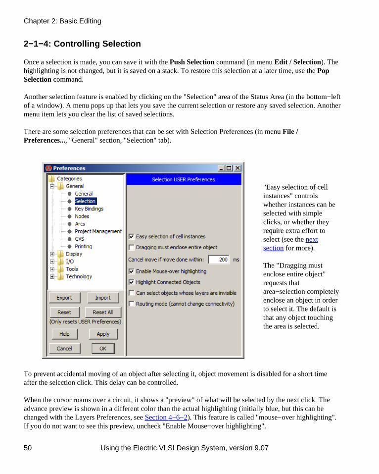
2−1−4: Controlling Selection
Once a selection is made, you can save it with the Push Selection command (in menu Edit / Selection). Thehighlighting is not changed, but it is saved on a stack. To restore this selection at a later time, use the PopSelection command.
Another selection feature is enabled by clicking on the "Selection" area of the Status Area (in the bottom−leftof a window). A menu pops up that lets you save the current selection or restore any saved selection. Anothermenu item lets you clear the list of saved selections.
There are some selection preferences that can be set with Selection Preferences (in menu File /Preferences..., "General" section, "Selection" tab).
"Easy selection of cellinstances" controlswhether instances can beselected with simpleclicks, or whether theyrequire extra effort toselect (see the nextsection for more).
The "Dragging mustenclose entire object"requests thatarea−selection completelyenclose an object in orderto select it. The default isthat any object touchingthe area is selected.
To prevent accidental moving of an object after selecting it, object movement is disabled for a short timeafter the selection click. This delay can be controlled.
When the cursor roams over a circuit, it shows a "preview" of what will be selected by the next click. Theadvance preview is shown in a different color than the actual highlighting (initially blue, but this can bechanged with the Layers Preferences, see Section 4−6−2). This feature is called "mouse−over highlighting".If you do not want to see this preview, uncheck "Enable Mouse−over highlighting".
Chapter 2: Basic Editing
50 Using the Electric VLSI Design System, version 9.07

When a node is selected, all connected circuitry is also selected. To disable this, uncheck "HighlightConnected Objects".
When all of the layers of a node or arc are made invisible, the nodes and arcs are not selectable. To allowsinvisible nodes and arcs to be selectable, check "Can select objects whose layers are invisible". See Section4−5−3 for more on layer visibility.
"Routing mode (cannot change connectivity)" is a state in which nodes cannot be selected, and no changes tothe circuit are allowed. See Section 9−6−1 for more on routing.
2−1−5: Easy and Hard Selection
In a busy circuit, many objects may overlap, causing confusion when selecting. To simplify selection, objectscan be marked so that they are no longer easy−to−select, which means that standard selection does not workon them.
To select hard−to−select objects, use the Toggle Special Select command(in menu Edit / Modes / Select). You can also click on the "Special Select"tool bar button to enable "special selection". Once in this mode, all objectsare selectable.
Ease of selection extends to more than just nodes and arcs. There are four "classes" of objects that can beselected:
Basic objects (all arcs, primitive nodes, and port names) • Cell instances • Node and arc text (names and other text placed on nodes and arcs) • Instance names (an unexpanded cell instance's name) •
By default, the first three classes are easy−to−select, and instance names are hard−to−select. If you uncheck"Easy selection of cell instances" in the Selection Preferences dialog, then cell instances becomehard−to−select.
Although all nodes and arcs are typically easy−to−select, you can control them individually by uncheckingthe "Easy to Select" field in their properties dialog (use the Object Properties... command in menu Edit /Properties). If multiple objects are selected, the Object Properties... dialog has a popup on the right forchanging their selection difficulty.
Special commands exist in the Selection menu for dealing with easy−to−select nodes and arcs. You canselect all of the easy−to−select objects in the current cell with the Select All Easy command. Similarly, youcan select those that are not easy−to−select with the Select All Hard command. To change the ease ofselection for a set of objects, highlight them and use either Make Selected Easy or Make Selected Hard.
Chapter 2: Basic Editing
Using the Electric VLSI Design System, version 9.07 51

2−2: Circuit Creation
2−2−1: Node Creation
Node creation is done by selecting a node from the component menu in the side bar (on the left). Nodes inthe component menu are outlined in blue. After clicking on one of these nodes, click in the edit window toplace the node. If you hold the Control key, the node location will snap to one of the axes.
The location of the cursor is aligned to the nearest grid unit. This adjustment can be controlled with the GridPreferences (in menu File / Preferences..., "Display" section, "Grid" tab, see Section 4−7−2).
When placing a node, the cursor points to the anchor point of the newly created node. This is the center (forprimitives) or the location of the cell−center (for cell instances). Cell instances can change their anchor pointby moving the Cell−Center node inside of their layout (see Section 3−3).
When placing a node, but before you click to actually create the node, it is possible to temporarily switchfrom node−placement to zoom/pan mode. This allows you to better select the location of the newly−creatednode. To temporarily zoom, type "z", zoom the display, and then type "z" again to finish placing the node. Totemporarily pan, type "p", pan the display, and then type "p" again to finish placing the node. For more onzooming and panning, see Sections 4−4−1 and Sections 4−4−2.
Besides basic components, there are special entries in the component menu for creation of additional nodes:
The "Cell" button displays a list of cell instances that can be created (see Section 3−3).• The "Pure" button (only available in layout technologies) lets you place pure−layer nodes (seeSection 6−10−1).
•
The "Spice" button (only available in schematics) lets you place Spice primitives (see Section9−4−3).
•
Chapter 2: Basic Editing
52 Using the Electric VLSI Design System, version 9.07

The "Misc" button has a collection of special objects that can be created.•
"Cell Instance..." brings up a dialog toselect a cell instance to place (see Section3−3).
•
"Annotation Text" places a node thatcontains only text (see Section 6−8−1).This can also be accomplished with theAdd Text Annotation command (inmenu Edit / Text)
•
"Layout Text..." brings up a dialog tocreate text from layout nodes (see Section6−10−3).
•
"Layout Image..." brings up a dialog tocreate an image from layout nodes (seeSection 6−10−3).
•
"Annular Ring..." brings up a dialog tocreate circular shapes (see Section6−10−3).
•
"Cell Center" places a node that definesthe origin of the cell (see Section 3−3).
•
"Essential Bounds" places a node thatdefines the corners of the cell's essentialbounds (see Section 7−6−3).
•
"Spice Code" places a text−only node that will be inserted into Spice decks (see Section 9−4−3).• "Spice Declaration" places a text−only node that will be inserted into Spice decks near the top (seeSection 9−4−3).
•
"Verilog Code" places a text−only node that will be inserted into the code area of Verilog decks (seeSection 9−4−2).
•
"Verilog Declaration" places a text−only node that will be inserted into the declaration area ofVerilog decks (see Section 9−4−2).
•
"Verilog Parameter" places a text−only node that will be inserted after the "module" header of thiscell so that a parameter can be defined (see Section 9−4−2).
•
"Verilog External Code" places a text−only node that will be inserted outside of any "modules" sothat arbitrary external code can be inserted (see Section 9−4−2).
•
"Simulation Probe" places a node that can be used to display simulation results (see Section 4−11).• "DRC Exclusion" places a node that hides geometry from DRC examination (see Section 9−2−3).• "AFG Exclusion" places a node that tells Auto−Fill Generation to ignore the area (not currently used,but see Section 9−8−2 for more on Auto−Fill Generation).
•
"Invisible Pin" places an invisible−pin node (see Section 7−6−3).• "Universal Pin" places an universal−pin node (see Section 7−6−3).• "Unrouted Pin" places an unrouted−pin node (see Section 7−6−3).•
Chapter 2: Basic Editing
Using the Electric VLSI Design System, version 9.07 53

2−2−2: Arc Creation
As the introductory example showed, arcs are created by clicking the right button. This can actually functionin two different ways, depending on what is highlighted.
Segment Wiring
If one node is highlighted, segment wiring is done, in which an arc is drawn from the highlighted node to thelocation of the cursor. If there is nothing at that location, a pin is created, and it is left highlighted. Using theright button again runs an arc from that pin to another location. By clicking and holding the right button, youcan see the path that the new arc will follow.
In general, all wiring operations should be done by clicking and holding the right button, then moving thecursor until the intended wiring is shown, and finally releasing. This is recommended because wiring is quitecomplex and can follow many different paths.
If you type a digit key while the right button is pressed, it changes the wiring layer by inserting contacts tothat layer of metal. For example, if you are running a metal−1 wire, and type "3" during the wiring, then twocontacts will be added (metal−1−metal−2 and metal−2−metal−3) to make the wire run in metal−3.
If the cursor is over another object when the right button is released, the new wire attaches to that object. Ifthere are multiple objects under the cursor, press the space bar (while the right button is pressed) to cyclethrough the possible endpoints (including the possibility of connecting to none of them). To prevent the wirefrom connecting to anything under the cursor, hold the control key while routing.
If an Unrouted arc is attached to the original node, that arc moves to the new pin. This allows you to replaceUnrouted arcs incrementally, one segment at a time. When both ends of the Unrouted arc are replaced by asegment, that arc is removed. See Section 9−6−1 for more about Unrouted Arcs.
Two−Point Wiring
The other way that the creation button can operate is two−point wiring, in which two nodes are highlightedand one or more arcs are created to connect them. Highlighting of these two nodes is done by clicking theleft button over the first one, and then using the shift−left button on the second. Note that if the second nodeis obscured by other objects, you can cycle through the objects under the cursor with thecontrol−shift−left button. Once the two nodes are highlighted, use the right button to wire them together.Note that the highlighted ports on the selected nodes are important: arcs will run between them, so they mustbe compatible in their wiring capabilities.
Two−point wire creation first attempts to run a single arc. Generally, this can happen only if the ports arelined up accurately. Failing single arc placement, an attempt is made to connect with two arcs and anintermediate node. These two arcs can bend in one of two directions, determined by the location of thecursor.
Chapter 2: Basic Editing
54 Using the Electric VLSI Design System, version 9.07

Special Considerations
In addition to running an arc between two nodes, you can also use arcs as the starting or ending point of arccreation.
If it is sensible, the creation command actually uses one of the nodes on an end of the selected arc. However,if the connection falls inside the arc, it is split and a new node is created to make a "T" connection.
Electric will allow you to connect two nodes or arcs as long as there is some way in the current technologyfor those objects to be connected. For example, if connecting between metal−1−pin and a metal−3−pin in theMOSIS CMOS technology, Electric will place metal−1−metal−2 and metal−2−metal−3 contact cuts down,and wire between all four nodes. When vias are inserted, they are placed closest to the "destination" node (orfarthest from the original node).
As mentioned in Section 1−8, pressing the number keys for a valid layer switches to that layer. If a node ishighlighted, it will route to that layer from the node, creating contacts as necessary.
Chapter 2: Basic Editing
Using the Electric VLSI Design System, version 9.07 55

2−2−3: Special Cases
The default width is set by the Arcs Preferences (in menu File / Preferences..., "General" section, "Arcs"tab). If there are other arcs of this type already connected to the new one, and they are wider than normal,then the new arc will use that width. Also, if an arc connects to a node that is wider than normal, it will growto match the size of the node (this can be disabled in the Arc Preferences, see Section 5−5).
Note that all arcs overlap their endpoint by half of their width, so very wide arcs may overlap theirdestination with too much geometry. You can turn off this overlap by using the Toggle End Extension ofHead and Toggle End Extension of Tail commands (in menu Edit / Arc). See Section 5−4−3 for more onend extension.
An unusual circuit creation command is theInsert Jog In Arc command (in menu Edit /Arc). This command inserts a jog in thehighlighted arc by replacing it with three newarcs. Two of the new arcs run to the location ofthe cursor, and the third arc is perpendicular tothem, connecting the ends at the cursor location(initially it has zero length).
Once the jog is inserted, either half of the arc may be moved without affecting the other half, and theperpendicular arc will keep the circuit connected.
Beginning users often leave many extra pins in their circuits. With the Cleanup Pins command (in menuEdit / Cleanup Cell), these pins are automatically removed from your circuit, leaving a cleaner network. Thecommand does other pin organizations, such as making sure that text on these pins is located correctly,identifying zero−sized pins, and identifying oversized pins. The Cleanup Pins Everywhere command doesthis function for all cells at once.
The Connect Arcs that Cross Named Network... command (in menu Edit / Arc) looks for arcs thatintersect a specified network and forces them to connect to the network. For example, if a network consists ofa Metal−2 arc, and a Metal−3 arc crosses that network, then a via will be inserted at the intersection point toconnect the arcs. This command actually breaks the intersecting arcs and inserts a contact node so that thecircuit is in proper form.
Chapter 2: Basic Editing
56 Using the Electric VLSI Design System, version 9.07

2−3: Circuit Deletion
To remove circuitry, select nodes and/or arcs and use the Selected command (in menu Edit / Erase). Akeyboard shortcut for this is the Delete key. If there is a highlighted area rather than a highlighted object,everything in the area is erased.
Note that an arc always connects two nodes, and therefore it cannot remain if one of the nodes is gone. Thismeans that certain rules apply to circuit deletion:
When a node is erased, all connecting arcs are also deleted. However, if a node is deleted that hasexactly two arcs, connected as though the node were in the middle of a single arc, then the node andtwo arcs are replaced with a single arc.
•
In the interest of cleanliness, if an arc is erased, any isolated pins are also erased.• If an erasednode has anexport on it (asin thisexample), thenthe exportdisappears andso do all arcsconnected tothe port oninstances ofthe current cell(for moreinformation onhierarchy, seeChapter 3).
•
The exception to these rules is the Nodes Preference "Reconstruct arcs and exports when deleting instances"(see Section 6−2) which requests that when a cell instance is deleted, and it has arcs connected to it orexports from it, these arcs and exports will be "reconstructed" so that they continue to exist. Reconstructionconsists of creating pins where the cell instance ports used to be so that the arcs and exports can continue toexist.
Chapter 2: Basic Editing
Using the Electric VLSI Design System, version 9.07 57

When an area is selected instead of objects(see Section 4−7−2) the Edit / Erase /Selected command erases all geometry inthe highlighted area. All arcs that cross intothat area will be truncated. Thus, thiscommand erases precise geometry,independent of the structure of nodes andarcs. Note that the area to be erased isadjusted by the current alignment values(see Section 4−7−2).
Two special arc deletion commands are Arcs Connected to Selected Nodes and Arcs Connected BetweenSelected Nodes (in menu Edit / Erase). The first command removes all arcs that have either end on aselected node. The second command removes all arcs that have both ends on selected nodes.
Chapter 2: Basic Editing
58 Using the Electric VLSI Design System, version 9.07

2−4: Circuit Modification
2−4−1: Movement
Components can be moved by clicking on them with the left button and then dragging them around whilekeeping the button pressed. During the drag, the new location of the components will be shown (as well asthe amount of motion), and once the button is released the circuitry will be moved.
While moving, simple design−rules areapplied and a warning is shown if the objectis in violation. In the example here, theMetal−1−Metal−2 contact is moved downtoward the Metal−1 arc and is too close. UseDRC Preferences to control these errormessages (see Section 9−2−2).
Another way to move objects is to use the arrow keys. When a node or arc is selected, each press of an arrowkey moves that object by one grid unit. If the shift key or the control key is held, then the arrow keys movethe object by a block of grid units. A block of grid units is defined in the Grid Preferences (in menu File /Preferences..., "Display" section, "Grid" tab) to be the frequency of bold dots in the grid, initially 10. If youhold both the shift key and the control key, then the distance moved will be a block squared (i.e. initially100). Note that these arrow keys are available in the Edit / Move menu with the commands Move ObjectsLeft/Right/Up/Down for a single unit, Move Objects More Left/Right/Up/Down for a block of units, andMove Objects Most Left/Right/Up/Down for a squared−block of units. Also note that the amount moved isalways grid−aligned (useful when squaring the block amount causes off−grid distances).
The distance that the arrow keys move is also affected by the gridalignment setting (see Section 4−7−2). The current alignment/movement isshown, and there are buttons to increase or decrease the size.
Clicking on the size amount brings up a menu that lets you change to any of the 5 movement/alignment sizes,or bring up the Preferences dialog for further control. Note also that the "f" key increases the size by one stepand the "h" key decreases the size by one step.
To move objects along only one line (just horizontally or vertically but not both), hold the Control key downduring motion. Note that holding the Control key down before clicking will change the nature of the mouseaction, so you must click first, and then press Control. When editing schematics, this will constrain objects tomovement along 45 degree angles.
When arcs are moved by a large amount, they cause the connecting nodes to move with them. However, forsmall arc motion, the arc may shift within its ports. This can only happen if the port has nonzero area and if
Chapter 2: Basic Editing
Using the Electric VLSI Design System, version 9.07 59

the arc has the slidable constraint (shown with the letter "S" when highlighted). These constraints arediscussed in greater detail in Section 5−2−2.
2−4−2: Other Modification
Another way to move a node is to usethe Object Properties... command (inmenu Edit / Properties), and type newX and Y positions. This dialog allowsother modifications to be made as well(orientation, etc.)
The dialog shows the location of theanchor−point of the node.
The dialog also has a field for the node's name. This name is not related to network information, but it mustbe unique, and can be used for identification. If a schematic node is given an arrayed name (such as"and[0:3]") then it indicates that the node is arrayed that many times. Nodes (and arcs) are automaticallygiven unique names when first created (such as "nmos@0").
Chapter 2: Basic Editing
60 Using the Electric VLSI Design System, version 9.07

The Object Properties dialogis modeless: it can remain onthe screen while other editingis being done. If a differentnode is selected, the dialogupdates to show that node'sinformation. The "Apply"button changes the selectednode to match the new valuestyped into the dialog.
The ObjectProperties... dialog can alsoexpand to show moreinformation. When the"More" button is clicked, itgrows to full size as shown.The full size ObjectProperties... dialog has manynew controls, which varyaccording to the type of nodeselected:
"Expanded" and "Unexpanded" control how the node is drawn (if it is a cell instance). An expandedinstance is one that shows its contents; an unexpanded instance is drawn as a black box (see Section3−4).
•
"Easy to Select" sets whether this node is selectable with a simple click. This feature allows you toeliminate pieces of circuitry from active editing (see Section 2−1−5).
•
"Invisible Outside Cell" indicates that this node will not be drawn when the current cell is viewedfrom higher−up the hierarchy.
•
"Locked" nodes may not be changed (moved, deleted).•
The bottom of the expanded Object Properties... dialog has a scroll area that can view "Ports","Parameters", or "Bus Members on Port". By default, a list of the node's ports is shown, including anyexports, connections, and highlight details. The "See" button selects the selected object in the list, either aport or an arc. If the "Parameters" button is selected, the list shows the parameters on the node. When"Parameters" is selected, the entries in the list let you modify individual values. Note that there is also an"Edit Parameters" button, which brings up a full dialog for editing them. See Section 6−8−5 for more onParameters. The last button, "Bus Members on Port" lists all of the signals found on the currently selectedbus port (see Section 6−9−3 for more on busses).
In some situations, the list may be too large to display easily (for example, a cell instance with hundreds ofports). When the list contains more than 100 entries, only the first 100 are shown, and the "Show All" buttonis available to show the entire list.
Chapter 2: Basic Editing
Using the Electric VLSI Design System, version 9.07 61

If many objects are selected, you can move them by a specific distance with the Move ObjectsBy... command (in menu Edit / Move).
If many nodes are selected, the Object Properties... command will list all of them, and allow appropriatechanges to be made (depending on what is selected).
Changes are only made in the fields where you type a value. To remove an item from the list of selectedobjects, use the "Remove" button. To remove all but the selected item, use "Remove Others". If only twoobjects are selected, this dialog shows the distance between their centers.
Chapter 2: Basic Editing
62 Using the Electric VLSI Design System, version 9.07

2−5: Changing Size
2−5−1: Node Sizing
To change the size of a node, select it and use the Interactively command (in menu Edit / Size).
The command will show 8 handles around the node, fourin the corners and four on the sides. Clicking anddragging on any handle will resize the nodeappropriately. When you release the button, the nodechanges size. If multiple nodes are selected, only one hasthe handles but all are resized.
While stretching the node, hold the Control key to constrain the size to just one axis, and hold the Shift key toconstrain the X and Y sizes so that they scale uniformly. If you hold the Control and Shift keys, then the nodewill resize about its center.
It is recommended that you hold the mouse button down while dragging so you can see the final size of thenode. Release the mouse button to actually resize the node. To abort this operation, type Escape.
Another way to change the size of one or morenodes is to select them and use the All SelectedNodes... command (in menu Edit / Size). Thedialog allows you to set the X and Y sizes of theselected nodes. If you leave one of these size fieldsempty, that coordinate is not changed.
Note that when typing size amounts into a dialog, specify the size of the highlighted area. In a typical MOStransistor, the highlighted area (where active and polysilicon cross) is 2x3, even though the component ismuch larger if you include the four overlap regions sticking out.
Chapter 2: Basic Editing
Using the Electric VLSI Design System, version 9.07 63

2−5−2: Arc Sizing
To change the width of an arc, issue the Interactively command (in menu Edit / Size). Note that the arcstretches about its center so that an edge is at the cursor location. Click a button to make the change. Tochange the size of more than one arc at a time, select the arcs and use the All Selected Arcs... command.
Another way to change an arc's width isto select it and use the ObjectProperties... command (in menu Edit /Properties).
Note that when typing size amounts intoa dialog, specify the size of thehighlighted area. A CMOS active arcshows highlighting only on its activearea, even though the complete arc hasimplant regions that are much larger.
The "Name" field lets you name an arc(see Section 6−8−1). Arc names areonly displayed on the arc if they havebeen explicitly typed into this dialog.You can also use the "Props." button toshow a dialog that controls all aspectsof a displayed arc name.
The "Easy to Select" checkbox enablesselection of the arc with a simple click(see Section 2−1−5).
Many pieces of state can be changed here, including Rigid and Fixed−angle (see Section 5−2−1), Slidable(see Section 5−2−2), Directionality (see Section 5−4−1), Ends extension (see Section 5−4−3), and Negation(see Section 5−4−2).
When an Artwork arc has been selected (see Section 7−6−1), the "Color and Pattern..." button is available forsetting its color.
Chapter 2: Basic Editing
64 Using the Electric VLSI Design System, version 9.07

2−6: Changing Orientation
There are two commands that can be used to change the orientation of circuitry. The Rotate command (inmenu Edit) has a submenu that allows the currently highlighted objects to rotate in any of three Manhattandirections or by an arbitrary amount.
The Mirror command (in menu Edit) has a submenu that allows you to flip the currently highlighted objectsabout their vertical centerline (left/right mirroring) or their horizontal centerline (up/down mirroring).
For individual nodes, the Object Properties... dialog (in menu Edit / Properties) lets you control its rotationand mirroring.
Be aware that mirroring is not the same as rotating, even though both may produce the same visual results.Mirroring causes the node to be flipped about its horizontal or vertical centerline, and thus appear backwards.
Chapter 2: Basic Editing
Using the Electric VLSI Design System, version 9.07 65

Chapter 2: Basic Editing
66 Using the Electric VLSI Design System, version 9.07

Chapter 3: Hierarchy
3−1: Cells
A collection of nodes and arcs is called a cell, and instances of cells can be placed in other cells. When a cellinstance is placed, that instance is also a node, and is treated just like the simpler transistor and contact nodes.Thus, nodes come in two forms: primitive and complex. Primitive nodes are found in the component menuand are pre−defined by the technologies (transistors, contacts, pins). Complex nodes are actually instances ofother cells, and are found in libraries.
Electric gives each cell a view and a version and organizes cells into cell groups. A cell's view describes itscontents (for example "layout", "schematics", "netlist", etc.) A cell's version defines its design age. The fullname of a cell is:
CELLNAME;VERSION{VIEW}
where CELLNAME is the name of the cell, VIEW is the abbreviated name of this cell's view, and VERSIONis the version number of this view of the cell. When no version number is specified, it implies that this cell isthe most recent version (has the largest number). Thus, the cell "gate;2{lay}" is more recent than"gate;1{lay}" but less recent than "gate{lay}" (which must have a higher version number, probably 3).
In the above example, there is a library with two cell groups. One group has a set of cells called "gate" andthe other has a set of cells called "latch". On the right is the explorer view of these cells. See Section4−5−2 for more on the cell explorer.
Using the Electric VLSI Design System, version 9.07 67

Although it is not necessary for cells in a group to all have the same name, the system presumes that commonnames will be grouped together. Once in a group, you can rename a cell to give it a different name than theothers in its group. Use the Rename Cell... command (in menu Cell). You can also use context menus in thecell explorer to rearrange groups.
Chapter 3: Hierarchy
68 Using the Electric VLSI Design System, version 9.07

3−2: Cell Creation and Deletion
Cells are created with the NewCell... command (in menu Cell).
The New Cell... command requestsa new cell name as well as its viewand technology. You can choose toshow the cell in the current window,or create a new one.
Cell names may not contain spaces,tabs, curly braces, semicolons,unprintable characters, or a colon.
Another way to create a new cell is to make a copy of an existing one. The Duplicate Current Cell... andDuplicate Cell... commands (in menu Cell) copy a cell to a different one with a new name (you will beprompted for the new name). The New Version of Current Cell command makes a copy of the cell in thecurrent window, but since it is a "new version", it has the same cell name. The newly created cell is displayedin the window.
Once cells are created you can edit them with the Edit Cell... command (in menu Cell). Cells can also beedited by using the cell explorer (see Section 4−5−2 for more).
Chapter 3: Hierarchy
Using the Electric VLSI Design System, version 9.07 69

To delete a cell, use the DeleteCell... command (in menu Cell). Whendeleting a cell, there cannot be anyinstances of this cell, or the deletion fails.As a side effect of failure, you are shown alist of all other cells that have instances ofthis, so you can see the extent of its use.To find out whether a cell is being usedelsewhere in the hierarchy, use the ListCell Usage command (in menu Cell / CellInfo). For an explanation of the "EvaluateNumbers when Sorting Names" checkbox,see Section 3−7−1.
Because Electric is able to keep oldversions of cells, deleting the latestversion will cause an older version tobecome the "most recent". Old versionsare those whose cell names include the";VERSION" clause indicating that thereis a newer version of this view of the cell.
For example, if you have cell "Adder" and an older version "Adder;1", then deleting "Adder" will cause"Adder;1" to be renamed to "Adder". This might make you think that the deletion failed, because there is stilla cell called "Adder", but this cell is actually the older (but now most recent) version.
To clean−up old and unused versions of cells, use the Delete Unused Old Versions command (in menuCell). Any such cells that are no longer used as instances in other cells will be deleted from the library. Youwill get a list of deleted cells, and it is possible to undo this command.
Chapter 3: Hierarchy
70 Using the Electric VLSI Design System, version 9.07

3−3: Creating Instances
To place an instance of a cell in another cell, use the "Cell" button in the component menu. After choosing acell from the popup list, click in the edit window to place the instance.
Another way to place an instance of acell is to use the Place CellInstance... command (in menu Cell).You will be shown a list of cells thatare available for creation. Afterselecting one, click to create aninstance in the current cell.
The cell selection dialog has threecontrols at the top for viewing cells.The "Library" popup lets you choosewhich library to examine. You canchoose "ALL" to see cells from alllibraries. The "View" popup lets yousee only those cells in the specifiedview. Again, you can choose "All" tosee all views. The "Filter" fieldcontains a regular expression thatmust match a cell name in order to listit. For an explanation of the "EvaluateNumbers when Sorting Names"checkbox, see Section 3−7−1.
If you place an instance from a different library, that library will be linked to the current one. Linked librariesare read from disk together, and form a single hierarchy that spans multiple files. See Section 3−9−1 for moreon libraries.
An alternate way to create a cell instance is to duplicate an existing one on the screen. This requires that aninstance of that particular cell already exist. Select the existing cell and use the Duplicate command (in menuEdit). Then move the cursor to the intended location of the new instance and click to create the copy. Notethat this command copies all attributes of the original node including its orientation.
Chapter 3: Hierarchy
Using the Electric VLSI Design System, version 9.07 71

When a cell instance isbeing created, the cursorpoints to its anchorpoint. The anchor pointis that point inside of thecell where thecoordinate space has itsorigin. This is oftendefined by the locationof a cell−center nodeinside of the cell (seeSection 7−6−3).
Most cells have a cell−center node placed automatically in them. If there isn't one and you want it, click onthe "Misc" button in the component menu on the left, and choose "Cell Center". A cell−center node, placedinside of the cell definition, affects the anchor point for all subsequent creation of instances of the cell.
The cell−center is always at the origin of the cell. If you move it, then the origin moves (in other words,moving the cell center is really like moving everything else in the cell). Note that the cell center is "hard toselect" and can only be moved in "special select" mode (see Section 2−1−5). You can move the cell center tothe center of the selected objects by using the Cell Center to Center of Selection command (from menuEdit / Move).
Schematic Instances
When drawing schematics, you place instances of the icon cell, not the schematics cell. An icon cell can beautomatically created with the Make Icon View command (in menu View, see Section 3−11−4). The iconcell can then be edited to have any appearance (see Section 7−6−1).
Chapter 3: Hierarchy
72 Using the Electric VLSI Design System, version 9.07

3−4: Examining Cell Instances
When instances are initially created, they are drawn as black boxes with nothing inside. This form of instancedisplay is called unexpanded. When the instances show the actual layout inside of them, they are expanded.This distinction applies only in layout; schematic icons never show their actual contents.
To expand a cell instance, select it and use the commands of the Cell / Expand Cell Instances menu. TheOne Level Down command opens up the next closed level; the All the Way command opens up all levels tothe bottom; and the Specified Amount... lets you type a number of levels of hierarchy to expand. Thesecommands expand all highlighted cells. If a highlighted cell is already expanded, this command expands anysubcells inside of the instance, repeatedly down the hierarchy.
Once expanded, a cell instance will continue to be drawn with its contents shown until the commands of theCell / Unexpand Cell Instances command are used. These commands return cell instances to theirblack−box form, starting with the deepest subcells that are expanded at the bottom of the hierarchy. The OneLevel Up command closes up the bottommost expanded level; the All the Way command closes all levelsfrom the bottom; and the Specified Amount... lets you type a number of levels of hierarchy to close.
You can also use the expansion (opened eye) and unexpansion (closed eye)icons from the tool bar to expand and unexpand by one level.
The expansion information can also be controlled by using the Object Properties... command (in menu Edit/ Properties) and clicking on the "Expanded" or "Unexpanded" buttons.
There are times when you want to see the layout inside of a cell instance, but only temporarily. The LookInside Highlighted command (in menu Cell) displays everything in the highlighted area, down through allhierarchical levels. This is a one−shot display that reverts to unexpanded form if the window is shifted,scaled, or redrawn.
There is a slight difference in specification between the Expand Cell Instances commands and the LookInside Highlighted command. The Expand Cell Instances commands affect cell instances only, and thusany instances that are highlighted or in the highlighted area will be completely expanded. The Look InsideHighlighted command affects layout display in an area, so only those parts of instances that are inside of thehighlighted area will be shown. Thus, the command Look Inside Highlighted is more precise in what itexpands and can be used, in conjunction with Area selection, to show only a specific part of the circuit (seeSection 2−1−3 for more on area selection).
Chapter 3: Hierarchy
Using the Electric VLSI Design System, version 9.07 73

3−5: Moving Up and Down the Hierarchy
Each editing window in Electric displays a single cell. Editing changes can be made only to that cell, and notto any subcells that appear as instances. Thus, you may be able to see the contents of a cell instance, but youcannot edit it.
To edit a cell instance, use one of these commands in the Cell / Down Hierarchy menu:
Down Hierarchy descends into the definition of the currently selected cell instance. You will nowbe able to edit that cell.
•
Down Hierarchy, Keep Focus descends while keeping the same window zoom and pan.• Down Hierarchy, New Window creates a new window in which to show the lower−level cell.• Down Hierarchy, Keep Focus, New Window creates a new window in which to show thelower−level cell, while maintaining the zoom and pan factor.
•
The opposite of going down the hierarchy is the Up Hierarchy command (in menu Cell / Up Hierarchy),which pops you to the next higher cell in the hierarchy. If there was an associated DownHierarchy command, then this returns you to the place where you started, up the hierarchy. If the DownHierarchy commands were not used, Electric attempts to figure out the next higher cell in the hierarchy,switching icons for schematics where appropriate. If there are multiple possibilities (because the current cellis used in many locations) then you will be prompted for a specific location. An alternate version of thiscommand is Up Hierarchy, Keep Focus which moves up the hierarchy, but keeps the current cell's zoomand pan factors the same so that the circuitry does not move on the screen.
Besides traversing the hierarchy, you can also traverse the sequence of cells that has been edited. To edit thecell that was previously displayed, use the Go Back a Cell command (in the Cell / Cell ViewingHistory menu) and to go forward in the list, use the Go Forward a Cell.
These commands are also accessible from the tool bar "back" and"forward" buttons. If you right−click on these buttons, you are given a listof cells and can jump directly to one of them.
When going down or up the hierarchy, if an export or port is selected, then the equivalent port or export isshown after the level of hierarchy has changed.
Chapter 3: Hierarchy
74 Using the Electric VLSI Design System, version 9.07

Layout Considerations
If a layout cell is selected, you can use the Down Hierarchy In Place command to edit the cell whileshowing the upper level of the hierarchy. A red border is drawn around the cell now being edited and thesurrounding geometry at the upper level, which is not editable, is grayed−out. To change the border color,use the Layers Preferences (in menu File / Preferences..., "Display" section, "Layers" tab) and set the colorsfor the layer "SPECIAL: DOWN−IN−PLACE BORDER". To disable the graying−out of upper levels ofhierarchy, use the Display Control Preferences and uncheck "Dim upper levels of hierarchy when editingDown−In−Place".
The Down Hierarchy In Place To Object command finds the object under the cursor (at any level of thehierarchy) and descends to that level. This may go down the hierarchy many levels. It descends "in place" sothat the original geometry is visible, but higher−levels are grayed−out. It is useful when trying to quickly findthe hierarchy that exists at that point, and see which instances were used to construct it. Note that there maybe many different levels of hierarchy under the cursor, which will cause a popup to appear listing the possiblesubcells to edit.
Schematic Considerations
If an icon is selected, the Down Hierarchy commands will take you to the associated schematic. If the iconthat is selected is already in its own schematic (you can place an icon inside its own schematic fordocumentation purposes), then the Down Hierarchy command takes you to the actual icon so that you canedit it. The Down Hierarchy In Place command takes you directly to the icon, showing it in the context ofthe upper−level schematic.
Schematic nodes can be arrayed by giving them array names (see Section 6−9−3). When you descend into anarrayed node, the system does not know which element of the array you are entering. Most of the time, thespecific element is irrelevant, but if the circuit is being simulated, the specific instance may be necessary forcross−probing. Therefore, if the cell is being simulated and you descend into an arrayed node, you will beprompted for the specific element that you wish to visit.
There are other situations that cannot be detected, where the specific element needs to be known. To solvethis problem, you can request that Electric prompt for the specific element in all situations where an arrayednode is visited. To do this, check "Always prompt for index when descending into array nodes" in the NodesPreferences (in menu File / Preferences..., "General" section, "Nodes" tab)
Chapter 3: Hierarchy
Using the Electric VLSI Design System, version 9.07 75

3−6: Exports
3−6−1: Export Creation
All nodes in Electric have connection sites, called ports, which indicate where wires may be attached. Theprimitive nodes have predefined ports, but ports on cell instances must be defined by the user. To do this,simply select a port on a node inside the cell, and turn it into an export, which makes it available on allinstances of the current cell. Although most ports are on nodes along the edge of the cell, Electric makes noport location restrictions, so they may appear anywhere.
To see the location of all ports on the selected nodes, use the Show Ports on Node command (in menuExport). This command highlights the ports on the screen, using the global text scale to affect size (seeSection 6−8−4).
To create an export, select a porton a node and use the CreateExport... command (in menuExport). The resulting dialogrequests an export name andsome characteristics.
All export names on a cell must be unique; if a nonunique name is given, it is modified to be unique. Thismodification involves adding "_1", "_2", etc. to the end of scalar export names, or changing the index (from[1] to [2], etc.) for arrayed export names. Like cell names, export names may not contain spaces, tabs, orunprintable characters.
Behavioral characteristics can be associated with an export by selecting the appropriate field in the exportcreation dialog. These behavior characteristics are stored with the export and used primarily by simulators.The characteristics include the following:
Directional: "input", "output", and "bidirectional". • Supply: "power" and "ground". • Clocking: "clock" (a generic clock export) and "clock phase 1" through "clock phase 6". • Reference: "reference input", "reference output", and "reference base". In addition, reference exportscarry an associated export name that is used by the CIF netlister.
•
Chapter 3: Hierarchy
76 Using the Electric VLSI Design System, version 9.07

The "Always drawn" check box requests that the export label should always appear, regardless of theconnection or expansion of its cell. Typically, an export label on an instance of a cell is not displayed whenthat port is connected to an arc or when the instance is expanded. This check box overrides the suppression.
Another special check box, "Body only," requests that this export not appear when an icon is generated forthe cell. This is useful for power and ground exports or duplicate connection sites on a single network.
You can control exporting of allof the ports on the currentlyhighlighted node with theManipulate Ports onNode... command (in menuExport). This dialog shows allports, and lets you select sets ofthem for reexport.
There are many special exporting commands that are primarily used in array−based layout. If a cell instanceis replicated many times and the instances are wired together, then ports on the edge of the array are the onlyones that are not wired. These ports define the connections for the next level of hierarchy. What you want todo is to create exports for all unwired ports, automatically generating unique names. To do this, use thesecommands in menu Export:
Re−Export Everything reexports all ports on all nodes in the current cell. • Re−Export Selected reexports only ports on currently highlighted nodes:
Unwired Ports Only reexports only those ports that are not connected to an arc.♦ Wired and Unwired Ports reexports all ports.♦ Wired Ports Only reexports only those ports that are connected to an arc.♦
•
Re−Export Selected Port on All Nodes reexports the selected port on the every node in the cell thatis the same as the current one.
•
Re−Export Power and Ground reexports only Power and Ground exports.• Re−Export Highlighted Area reexports only ports inside the currently highlighted area (for precisearea selection, see Section 2−1−3):
Unwired Ports Only reexports only those ports that are not connected to an arc.♦ Wired and Unwired Ports reexports all ports.♦ Wired Ports Only reexports only those ports that are connected to an arc.♦
•
Re−Export Deep Highlighted Area reexports only ports inside the currently highlighted area, but•
Chapter 3: Hierarchy
Using the Electric VLSI Design System, version 9.07 77

goes all the way down the hierarchy, reexporting from the lowest level. This causes unconnectedexports deep down the hierarchy to become available for connection:
Unwired Ports Only reexports only those ports that are not connected to an arc.♦ Wired and Unwired Ports reexports all ports.♦ Wired Ports Only reexports only those ports that are connected to an arc.♦
Note that ports on primitive nodes are not exported with these commands. See Section 6−4 for more aboutarrays, and see Section 9−6−1 for more on automatic wiring.
Another special command for export creation is Add Exports from Library... (in menu Cell / MergeLibraries), which copies exports from another library into the current one. The other library is examined forcells whose names match ones in the current library. When a cell is found in the other library, all of itsexports are copied to the cell in the current library (if they don't already exist) and placed in the samelocation. This command is useful in managing standard cell libraries that are imported from other file formats(see Section 3−9−4 on Standard Cell Libraries). Because some formats contain geometry and others containconnectivity, this command is needed to put them together.
3−6−2: Export Information
Exports are selected by clicking on their text, or by clicking on the node from which they are exported. If avery dense design makes export selection hard, you can choose from a list by using the SelectObject... command (in menu Edit / Selection).
To see all exports that have been defined in the current cell, use the Show Exports command (in menuExport). This command highlights the exports on the screen, using the global text scale to affect size (seeSection 6−8−4).
The List Exports command gives the same information, but in text form, and the SummarizeExports command gives a text list that is reduced where sensible. To see a list of exports that are electricallyconnected to the current object, at multiple levels of hierarchy, use the List Exports on Network and ListExports below Network commands (in menu Tools / Network). To see a list of cells and networks wherethe currently selected export is used, higher up in the hierarchy, use the Follow Export UpHierarchy command.
Chapter 3: Hierarchy
78 Using the Electric VLSI Design System, version 9.07

Once a port has beenexported, its characteristicscan be modified by selectingthe export name and usingthe ObjectProperties... command (inmenu Edit / Properties).
You can change basic exportinformation such as thename, characteristic, andreference name (ifapplicable). You can controlexport state such as whetherit is always drawn, andwhether or not it appears onicons.
You can also change the appearance of the export by editing the size, font, color, style, anchor point, androtation of the name. See Section 6−8−1 for more about text appearance. See Section 6−8−4 for "smart"export text control.
Special buttons in the Export Properties dialog allow you to examine related objects. The "Highlight Owner"button shows the node on which this export resides.
You can change the characteristics of many exports at once by selecting them and using the ObjectProperties... command (in menu Edit / Properties). This multi−object dialog has popups that will change allexport characteristics at once. You can change the name of exports by using the Rename Export... command(in menu Export).
Chapter 3: Hierarchy
Using the Electric VLSI Design System, version 9.07 79

Displaying Ports and Exports
Ports and exports can bedisplayed on the screen inmany different ways. Tocontrol this, use thePorts/Exports Preferences (inmenu File / Preferences...,"Display" section,"Ports/Exports" tab).
The dialog offers three optionsfor ports and exports: "FullNames" shows full text names,"Short Names" shows port andexport names only up to thefirst nonalphabetic character,and "Crosses" shows crosses atthe locations.
With short names, the exports "Power−left" and "Power−1" are both written as "Power," which allowsmultiple exports with the same functionality but different names to be displayed as if they have the samename.
To remove port display completely, use the "Layers" tab of the side bar (see Section 4−5−3). In this panel areoptions to make exports text completely invisible.
Chapter 3: Hierarchy
80 Using the Electric VLSI Design System, version 9.07

3−6−3: Export Deletion and Movement
You can delete an export simply by selecting its name and using the Selected command of the Edit /Erase menu (or typing the Delete key). You can also use the Delete Export command (in menu Export).
To remove many exports at once, the Delete Exports on Selected command removes all exports on allhighlighted nodes. Also, the Delete Exports in Highlighted Area command removes only those exports thatare in the selected area. When an export is deleted, all arcs connected to that port on instances of the currentcell (higher up the hierarchy) are also deleted (see Section 2−3).
To move export text, simply select it and drag it. The location of the text has no effect on the location of theexport: moving the text is only for improvement of the display. However, if you check "Move node withexport name" in the Ports/Exports Preferences (in menu File / Preferences..., "Display" section,"Ports/Exports" tab), then moving an export name will cause the node (and the export) to move as well.
It is sometimes desirable to keep an export but to transfer it to another node. If a cell is in use higher in thehierarchy, unexporting and then reexporting deletes all existing connections. Instead, the MoveExport command (in menu Export) can be used. Before using this command, two nodes and their ports mustbe highlighted with left button and shift−left button. The export is moved from the first node to the secondnode.
You can control all existing exports inthe current cell with the ManipulateExports... command. This dialogshows the exports and lets you sortthem by name, layer, or characteristic.Schematic cells also offer a "bodyonly" control which, when checked,makes that export appear only in thebody (the schematic) and not in theicon cell (see Section 3−6−1). You canchange export names andcharacteristics.
If multiple exports are selected, changing one of their characteristics changes all of them. You can alsodelete, show, or renumber selected exports. Renumbering of exports presumes that the exports have numbersin their names and renames them so that there are no gaps in the sequence (and the first has no number). Forexample, the ports "gnd_7", "gnd_9", and "gnd_10" will be renamed "gnd", "gnd_1", and "gnd_2".
Chapter 3: Hierarchy
Using the Electric VLSI Design System, version 9.07 81

3−7: Cell Information
3−7−1: Cell Lists
To get some basic information about thecurrent cell (size, dates, etc) use theDescribe this Cell command (in menuCell / Cell Info).
To get information about more than onecell, use the General CellLists... command. The dialog selects asubset of the cells in the current library.
The section labeled "Which cells:" selectsthe cells to be listed (all, only those usedin other cells, only those NOT used in thecurrent cell, only those in the current cell,or only "placeholder" cells: those createdbecause of cross−library dependencyfailures, see Section 3−9−1).
The section labeled "View filter:" allowsonly certain views to be displayed.
The section labeled "Version filter:"allows removal of older or newer versionsof cells.
The section labeled "Display ordering:"controls the order in which the selectedcells will be listed.
The section labeled "Destination:" allowsyou to dump this listing to a disk file,formatted for spreadsheets(tab−separated).
The "Evaluate Numbers when Sorting Names" checkbox controls how cells are sorted (only relevant whencells are to be ordered by name). When checked, numbers inside of cell names are evaluated and sortednumerically. Thus, a set of cells called "A8", "A9", "A10", and "A11" will appear in that order. When not
Chapter 3: Hierarchy
82 Using the Electric VLSI Design System, version 9.07

checked, cells are sorted lexically, causing the cells to appear in this order: "A10", "A11", "A8", "A9".
The result of cell information listing looks like this:
−Cell−−−−−−−−−−−−Version−−−−Creation date−−−−−−−−−−Revision Date−−−−−−−−−Size−−−−Usage−−L−I−S−D
tech−Artwork{} 1 Dec 31, 1969 16:00:00 Dec 15, 2004 11:34:15 131.0x83.0 0 L
tech−Bipolar{ic} 1 Dec 15, 2004 11:34:25 Dec 15, 2004 11:34:25 10.0x12.0 1
tech−Bipolar{lay} 1 Jul 23, 1990 23:25:49 Dec 15, 2004 12:38:11 37.0x73.5 0
tech−Bipolar{sch} 1 Jul 26, 1990 23:58:58 Dec 15, 2004 11:34:27 58.75x59.5 0 L I
tech−DigitalFilter{} 1 Dec 31, 1969 16:00:00 Dec 01, 2000 13:56:47 48.0x45.5 0
tech−MOSISCMOS{lay} 1 Jul 24, 1998 16:10:55 Dec 09, 2001 12:35:29 85.5x83.0 0 D
tech−PCB7404{} 1 Dec 31, 1969 16:00:00 Dec 15, 2004 11:45:03 12.5x28.5 1
tool_NCC{sch} 1 Mar 27, 2001 06:35:49 Jan 25, 2002 15:57:57 44.0x41.5 0 L I
The last five columns show the usage and four state bits. The usage is the number of times that this cellappears as an instance in other cells. The state bits are:
"L" if the cell contents are locked• "I" if instances in the cell are locked• "S" if the cell is a standard cell• "D" if the cell has passed design−rule checking•
For more cell information, use the commands of menu Cell / Cell Info:
Summarize Cell Contents lists the nodes and layers used in the current cell.• Summarize Selected Cell Contents lists the nodes and layers used in the selected geometry.• List Nodes/Arcs in this Cell counts the number of nodes and arcs in current cell and below. This is ahierarchical count: if two cell instances each have two transistors inside of them, the total is 4transistors. However, it counts only actual nodes, ignoring arrayed nodes (see Section 6−9−3).
•
List Cell Instances shows all cell instances below the current cell.• List Cell Usage looks up the hierarchy and finds cells that contain the current cell as an instance.• List Cell Usage, Hierarchically looks up the hierarchy and finds cells that contain the current cell asan instance or as a subinstance. For example, if cell A contains cell B, and cell B contains cell C,then using this command on cell C will mention both cells A and B, whereas the nonhierarchicalversion of this command will mention only cell B.
•
Number of Transistors counts the number of transistors in the current cell and below (consideringarrayed instances, see Section 2−4−2).
•
Chapter 3: Hierarchy
Using the Electric VLSI Design System, version 9.07 83

3−7−2: Cell Graphing
Cell graphing shows the hierarchical structure of your circuit. The graph is stored in a new cell called"CellStructure", built from Artwork nodes.
The Cell Graph,EntireLibrary command (inmenu Cell / Cell Info)displays a graph ofevery cell in thelibrary. The CellGraph, FromCurrentCell commanddisplays a graph thatplaces the current cellat the top.
A cell graph can beedited like anythingelse in Electric. Clickand drag the cellnames to rearrange thegraph.
Electric can alsoconstruct a graph oflibrary dependencieswith the LibraryGraph command.
Chapter 3: Hierarchy
84 Using the Electric VLSI Design System, version 9.07

3−7−3: Cell Properties
To examine and set more information about cells, use the Cell Properties... command (in menu Cell): Theleft side of the dialog lists cells by library. On the right are the properties of the cells.
The checkbox "Disallow modification of anything in this cell", allows you to control whether the contents ofa cell is editable or not. When modification is disallowed, no changes may be made. This is useful when youwant to allow examination without accidental modification.
The checkbox "Disallow modification of instances in this cell", also prevents changes to the selected cell, butin this case, only instances of sub−cells are locked. This is useful when you have a correct instanceplacement and are doing wiring.
If you make a change that hasbeen disallowed, a dialogappears that asks if you wantto override the lock.
Chapter 3: Hierarchy
Using the Electric VLSI Design System, version 9.07 85

You may make the change ("Yes"), disallow the change ("No"), or remove the lock ("Always", whichunchecks the locks in this dialog).
The check box "Standard cell in a cell−library" indicates that this cell is a standard cell and should be treatedaccordingly. Verilog generation uses this information (see Section 9−4−2).
The check box "Part of technology editor library" indicates that this cell helps to define a technology. Formore on the technology editor, see Section 8−1.
The check box "Expand new instances of this cell" indicates whether newly created instances of this cell areexpanded (contents visible) or unexpanded (drawn with a black outline) See Section 3−4 for more onexpansion.
For the first 5 checkboxes in this dialog, there are buttons on the right which allow you to set or clear theseflags for all cells in the library.
Each cell is tied to a specific technology. The cell's technology is set when the cell is created. You canchange the technology that is associated with a cell by using the "Technology" popup.
The section labeled "For Textual Cells" lets you set the font and size of the text in that cell (see Section 4−9).
At the bottom is the cell frame control. The frame is a border that is usually drawn around schematics. Youcan set the frame size, whether it is wider (Landscape mode) or taller (Portrait mode), and whether a title boxis drawn in the corner. Additionally, you can set the designer name to be drawn for each cell. Otherinformation in the title box (company name, project name) are set on a per−user or per−library basis with theFrame Preferences (in menu File / Preferences..., "Display" section, "Frame" tab). See Section 7−5−2 formore on frames.
Chapter 3: Hierarchy
86 Using the Electric VLSI Design System, version 9.07

3−8: Rearranging Cell Hierarchy
In order to manipulate hierarchical circuits, it is useful to create and delete levels of the hierarchy. ThePackage Into Cell... command (in menu Cell) collects all of the highlighted objects into a new cell. You willbe prompted for the cell name. To package everything in an area, use the Area Selection commands (seeSection 2−1−3). When packaging an area, every node touching the area and all arcs between nodes in thearea are included in the new cell.
Packaging does not affect the highlighted circuitry. However, after packaging circuitry into a new cell, thatcircuitry can be deleted and replaced with an instance of the cell.
The opposite function is the removal of levels of hierarchy. This is done with the Extract CellInstance subcommands (in menu Cell), which takes the currently highlighted cell instances and replacesthem with their contents. The One Level Down subcommand just replaces the selected instances with theircontents. The All the Way subcommand continues to extract instances inside of instances until there are nomore instances, just primitives. The Specified Amount... prompts for a number of levels of hierarchy andextracts that many levels deep. All arcs that were connected to the cell instances are reconnected to thecorrect parts of the instantiated circuitry. Note that extraction works only with layout cells; it cannot be usedwith schematics.
Chapter 3: Hierarchy
Using the Electric VLSI Design System, version 9.07 87

3−9: Libraries
3−9−1: Introduction to Libraries
A library is a collection of cells that forms a consistent hierarchy. To enforce this consistency, Electric storesan entire library in one disk file that is read or written at one time. It is possible, however, to have multiplelibraries in Electric. Only one library is the current one, and this sometimes affects commands that work atthe library level. When there are multiple libraries, you can switch between them with the Change CurrentLibrary... command (in menu File) or by using the library's context menu in the cell explorer (see Section4−5−2). To see which libraries are read in, use the List Libraries command.
To create a new, empty library, use the New Library... command (in menu File). To change the name of thecurrent library, use the Rename Library... command. To delete a library, use the Close Library command.This removes only the memory representation, not the disk file.
It is possible to link two libraries by placing an instance of a cell from one library into another (this is donewith the Place Cell Instance... command in menu Cell). When this happens, the library with the instance(the main library) is linked to the library with the actual cell (this is the reference library). Because thereference library is needed to complete the main library, it will be read whenever the main library is read.
When there are many libraries used in the design of a circuit, it may be the case that a consistent set of libraryfiles is read into Electric, but that there are unused library files that have not been read. To detect thissituation, use the Find Unused Library Files (in menu File / Check Libraries). This command will look forunused library files in the disk directories used by the circuit and will report them to you so that the disk canbe cleaned−up. The command does not delete the library files: that is left to the user.
If referenced libraries are edited independently, it is possible that a reference to a cell in another library willnot match the actual cell in that library. When this happens, Electric creates a "placeholder" cell that matchesthe original specification. Thus, the link to the referenced library is broken because the cell there does not fitwhere the instance should be. To see a list of all placeholder cells that were created because of suchproblems, use the General Cell Lists... command (in menu Cell / Cell Info) and select "Only placeholdercells".
Electric comes with some built−in libraries:
There are two Spice primitive libraries (see Section 9−4−3). • A library of examples can be loaded with the Load Sample Cells Library command (in menuHelp). Another simple library can be found in the Load Library command (in menu Help / 3DShowcase).
•
A set of gates, useful for Logical Effort (see Section 9−9), can be loaded with the Load LogicalEffort Libraries (Purple, Red, and Orange) command (in menu Tools / Logical Effort).
•
Chapter 3: Hierarchy
88 Using the Electric VLSI Design System, version 9.07

Additional libraries are available at the Static Free Software website(www.staticfreesoft.com/productsLibraries.html).
3−9−2: Reading Libraries
The Open Library... command (in menu File) brings a new library into Electric from disk. These librariesmay have the extension ".elib", ".jelib", or ".delib" (the jelib format is the default, see Section 10−1). There isalso a Open Recent Library entry that lists all recently opened libraries.
You can also use the open−library icon from the tool bar.
Electric users with very old ".elib" files may have difficulty reading them into Electric. If you have beenusing versions of Electric prior to 7.00, it may help to upgrade to that version and read the libraries. Saving".elib" files from version 7.00 will work properly in the current system.
By default Electric searches for libraries in the working directory, absolute file path references, and Electric'sinternal library directory. Users can specify additional directories to search by using a file called "LIBDIRS"placed in the directory with the files being read. This file provides additional paths to search for library files.The file has the following syntax:
* <comments> include <another_LIBDIRS_file>
<library_directory>
Paths may be absolute or relative.
Besides Electric libraries, it is possible to read circuit descriptions that are in other formats with thesecommands in the File / Import menu:
Applicon 860 is a layout format from old Applicon EDA systems.• Bookshelf is an open format for specifying placement tasks.• CIF (Caltech Intermediate Format) is used to describe integrated circuit layout. It contains noconnectivity, so after the library is read, it does not know about transistors and contacts: just layers.You can use the node extractor to convert CIF to real Electric components (see Section 9−10−2). Toaffect how CIF is read, use the CIF Preferences (in menu File / Preferences..., "I/O" section, "CIF"tab). See Section 7−3−2 for more on CIF.
•
DEF (Design Exchange Format) is an interchange format that describes the contents of a library.DEF input often makes use of associated LEF files which must already have been read. Use theLEF/DEF Preferences (in menu File / Preferences..., "I/O" section, "LEF/DEF" tab) to affect howDEF is read (see Section 7−3−5).
•
DXF (AutoCAD) is a solid−modeling interchange format, and so it may contain 3D objects thatcannot be read into Electric. Nevertheless, Electric creates a library of artwork primitives as well as itcan. Use the DXF Preferences (in menu File / Preferences..., "I/O" section, "DXF" tab) to affect howDXF is read (see Section 7−3−7).
•
Chapter 3: Hierarchy
Using the Electric VLSI Design System, version 9.07 89

EDIF (Electronic Design Interchange Format) is used to describe both schematics and layout.Electric reads EDIF version 2 0 0. Use the EDIF Preferences (in menu File / Preferences..., "I/O"section, "EDIF" tab) to affect how EDIF is read (see Section 7−3−4).
•
ELIB is an older Electric library format that is in an undocumented binary format.• GDS II (Stream)... and GDS II (Stream) Skeleton are used to describe integrated circuit layout.The Skeleton version of the command reads only a skeletonized version of the top−level cell(bounding box and exports, no other content, see Section 3−11−2). This skeletonized cell also has apointer back to the original GDS file so that when it is written to disk, the full GDS can be mergedback in. GDS contains no connectivity, so after the library is read, it does not know about transistorsand contacts: just layers. You can use the node extractor to convert GDS to real Electric components(see Section 9−10−2). To affect how GDS is read, use the GDS Preferences (in menu File /Preferences..., "I/O" section, "GDS" tab). See Section 7−3−3 for more on GDS.
•
Gerber is a printed−circuit board artwork format. Use the Gerber Preferences (in menu File /Preferences..., "I/O" section, "Gerber" tab) to affect how Gerber is read (see Section 7−3−9).
•
LEF (Library Exchange Format) is an interchange format that describes the cells in a library. Thecells that are read in often contain only ports and very little contents. Use the LEF/DEF Preferences(in menu File / Preferences..., "I/O" section, "LEF/DEF" tab) to affect how DEF is read (see Section7−3−5).
•
Readable Dump is an older Electric library format that captures the entire database in atext−readable format. These files were used when the ".elib" file was the main way of savinglibraries, because a way was needed of reading library files. Now that the newer ".jelib" format isalso text−readable, there is no need to use Readable Dumps anymore.
•
Spice Deck (Single file) and Spice Decks (Whole directory) are input to the Spice simulator anddefine a netlist of circuitry. You can read a single file, or an entire directory (all .SPI files foundthere). See Section 9−4−3 for more on Spice. Reading Spice Decks will create wired instances, butthe placement of the instances will be automatically generated because that information is not in theSpice deck.
•
SUE (Schematic User Environment) is a schematic editor that captures a single cell in each file.The circuitry in SUE files is added to the current library instead of being placed in its own library(because many SUE files may have to be read to build up a single Electric library). When reading aSUE file, any subdirectories that start with "suelib_" will also be examined for dependent SUE cells.Use the SUE Preferences (in menu File / Preferences..., "I/O" section, "SUE" tab) to affect how SUEis read (see Section 7−3−8).
•
Text Cell Contents is used to read a text file into a text cell. The current window must be a textualview (such as VHDL, Verilog, documentation, etc.)
•
Verilog is a hardware description language used for simulation and fabrication. Electric reads theVerilog file and constructs a schematic representation. Because there is no placement in Verilog files,the schematic is topologically correct, but visually messy.
•
See Section 4−9 for more on text windows.
Some file formats (CIF, GDS, EDIF, LEF, DEF, SUE, and Applicon 860) are technology−specific. Beforereading them, you will be prompted for the layout technology to use. The default is to use the currenttechnology.
Chapter 3: Hierarchy
90 Using the Electric VLSI Design System, version 9.07

If you import a library that already exists in Electric, the following warning appears:
You can save the previous library, overwrite the previous library, cancel the operation, or merge the newlibrary into the previous library. The "Merge" option creates new versions of cells when the names conflict,producing a library that has both the previous and new contents in it.
3−9−3: Writing Libraries
Writing libraries to disk is done with the Save Library command (in menu File). The Save AllLibraries command writes all libraries that have changed.
You can also use the save−libraries icon from the tool bar.
To force all libraries to be saved,use the Mark All Libraries forSaving command, or use Save AllLibraries in Format... to specifyhow they are to be saved.
If a library was read from disk, itis written back to the same file. If,however, you wish to write thelibrary to a new file (thuspreserving the original) then usethe Save Library As... command.
The Library Preferences (in menuFile / Preferences..., "I/O"section, "Library" tab) offersoptions for writing libraries todisk. By default, saved librariesoverwrite the previous files and nobackup is created. If you choose"Backup of last library file", thenthe former library is renamed sothat it has a "~" at the end.
Chapter 3: Hierarchy
Using the Electric VLSI Design System, version 9.07 91

If you choose "Backup history of library files", then the former library is renamed so that it has its creationdate as part of its name.
Electric can also write external format files with these commands in the File / Export menu:
Bookshelf is an open format for specifying placement tasks.• CIF (Caltech Intermediate Format) is used to describe integrated circuit layout. The output filecontains only the current cell and any circuitry below that in the hierarchy. Use the CIF Preferences(in menu File / Preferences..., "I/O" section, "CIF" tab) to affect how CIF is written. See Section7−3−2 for more on CIF.
•
DFTM is a network interchange format for digital filters/transactional memory routers.• DXF (AutoCAD) is a solid−modeling interchange format. Use the DXF Preferences (in menu File /Preferences..., "I/O" section, "DXF" tab) to affect how DXF is written. See Section 7−3−7 for moreon DXF.
•
Eagle is an interface to the Eagle schematics design system (its netlist format). Before writing Eaglefiles, you must give every node the "ref_des" attribute, and every port on these nodes the "pin"attribute. If you also place the "pkg_type" attribute on the node, it overrides the cell name.
•
ECAD is an interface to the ECAD schematics design system (its netlist format). Before writingECAD files, you must give every node the "ref_des" attribute, and every port on these nodes the"pin" attribute. If you also place the "pkg_type" attribute on the node, it overrides the cell name.
•
EDIF (Electronic Design Interchange Format) can write either the Netlist or the Schematic viewof the circuit. Electric writes EDIF version 2 0 0. Use the EDIF Preferences (in menu File /Preferences..., "I/O" section, "EDIF" tab) to affect how EDIF is written. See Section 7−3−4 for moreon EDIF.
•
ELIB (Version 6) writes old−format binary files. These files can be read by version 6 of Electric.• GDS II (Stream) is also used to describe integrated circuit layout. The output file contains only thecurrent cell and any circuitry below that in the hierarchy. Use the GDS Preferences (in menu File /Preferences..., "I/O" section, "GDS" tab) to affect how GDS is written. See Section 7−3−3 for moreon GDS.
•
Gerber is a printed−circuit board artwork format.• HPGL is the Hewlett−Packard printing language. The output file contains only a visualrepresentation of the current cell (or part of that cell).
•
JELIB (Version 8.03) writes old−format JELIB files. These files are useful for versions 8.03 andearlier.
•
L is the GDT language, still appearing in some commercial systems. The output file contains onlythe current cell and any circuitry below that in the hierarchy.
•
LEF (Library Exchange Format) and DEF (Design Exchange Format) are interchange formatsthat describe a two−level layout. The lower level (the standard cells) are written to the LEF file. Thetop−level is written to the DEF file. If the hierarchy has more than two levels, then it is flattened andwritten all in the LEF file. See Section 7−3−5 for more on LEF and DEF.
•
Pads is an interface to the Pads schematics design system (its netlist format). Before writing Padsfiles, you must give every node the "ref_des" attribute, and every port on these nodes the "pin"attribute. If you also place the "pkg_type" attribute on the node, it overrides the cell name.
•
PNG (Portable Network Graphics) is an image format that captures the current window.• PostScript is the Adobe printing language. The output file contains only a visual representation of•
Chapter 3: Hierarchy
92 Using the Electric VLSI Design System, version 9.07

the current cell (or part of that cell). PostScript options can be controlled with the PrintingPreferences (in menu File / Preferences..., "General" section, "Printing" tab).Flattened Rectangles is a general format for writing flattened geometry as rectangles. Users areprompted for the format to use, with %l replaced by the rectangle layer, %x replaced by the Xcoordinate of the center of the rectangle, %y replaced by the Y coordinate of the center of therectangle, %w replaced by the width of the rectangle, and %h replaced by the height of the rectangle.
•
STL (Stereolithography) is a format for interfacing with "3D printing" machines.• SVG is a web format (Scalable Vector Graphics) that captures the current window. See Section7−3−10 for more on SVG.
•
Telesis is an old netlist interface. Each cell in the circuit is saved to a separate Telesis file with the".txt" extension.
•
Text Cell Contents is used to write a text file from a text cell. The current window must be a textualview (such as VHDL, Verilog, documentation, etc.) See Section 4−9 for more on text windows.
•
The exported files from Electric are often considered to be proprietary information, and must be markedappropriately. Copyright information can be inserted into exported files with the Copyright Preferences (inmenu File / Preferences..., "I/O" section, "Copyright" tab).
Since each export file has a different format for comments, the copyright text should not contain any suchcharacters. Instead, the system will insert the proper comment characters for the particular export format.
Chapter 3: Hierarchy
Using the Electric VLSI Design System, version 9.07 93

The copyright information will be inserted into decks exported for CIF, LEF, and PostScript, as well as insimulation netlists for Verilog, Spice, Silos, ESIM/RSIM/RNL/COSMOS, FastHenry, Maxwell, and IRSIM.
3−9−4: Standard Cell Libraries
Electric comes with few useful libraries for doing design (see Section 3−9−1). However, the system is able tomake use of Artisan libraries. These libraries are free, provided that you sign an Artisan license. Once youare licensed, you will have standard cell libraries, pad libraries, memory libraries, and more.
Artisan libraries are not distributed in Electric format. Instead, they come in a variety of formats that can beread into Electric. The GDS files contain the necessary geometry, and the LEF files contain the connectivity.By combining them, Electric creates a standard cell library that can be placed−and−routed and can befabricated. Note that the data is not node−extracted, so not all of Electric's capabilities can be used with thisdata.
To create an Artisan library, follow these steps:
Select the Artisan data that you want, and extract the GDS and LEF files for it. The GDS files willhave the extension ".gds2", which is not what Electric expects (Electric expects them to end with".gds"), so you may want to rename them.
•
Read the LEF file into Electric with the LEF (Library Exchange Format)... command (in menuFile / Import). Keep in mind that the LEF data may come in multiple versions for different numbersof metal layers.
•
Read the GDS data into Electric with the GDS II (Stream)... command (in menu File / Import).Note that the proper GDS layers must be established first (with the GDS Preferences, see Section7−3−3). There will now be two libraries in memory: one with the GDS data and one with the LEFdata.
•
Merge the port information from the LEF library into the GDS library. It is important that the GDSlibrary be the "current library" (use the Change Current Library... command in menu File if it isnot). To merge the LEF port information, use the Add Exports from Library... command (of menuCell / Merge Libraries). You will be prompted for another library, and should select the one withthe LEF data.
•
At this point, the GDS library now has standard cells in it, including the export information that wasin the LEF library. Before saving it to disk, you should probably use the Cell Properties... command(of menu Cells, see Section 3−7−3) and set all of the cells to be "Standard cell in a cell library".
•
Chapter 3: Hierarchy
94 Using the Electric VLSI Design System, version 9.07

3−10: Copying Cells Between Libraries
In general, different libraries are completely separate collections of cells that do not relate. For example, twocells in different libraries can have the same name without being the same size or having the same content.Although a cell from one library can be used as an instance in another, this causes the two libraries to belinked together. It may be simpler to copy the cells from one library to another, thus allowing a single libraryto contain the entire design.
A simple way to copy cells from one library to another is to drag them in the Explorer window (see Section4−5−2).
A more powerfulmethod is theCross−LibraryCopy... command (inmenu Cell). Thiscommand provides adialog for copying cellsbetween libraries. Theleft and right columnsshow the contents oftwo different libraries(and the pulldownsabove each column letyou select the twolibraries that you wantto see).
Chapter 3: Hierarchy
Using the Electric VLSI Design System, version 9.07 95

When there is a cell with the same name in both libraries, the system compares them to determine which isnewer. If you check "Date and content" (and then "Compare" to do comparison again) Electric will comparethe actual contents of cells when determining their equality. Unchecking "Examine quietly" will cause thesystem to describe differences found during comparison.
By choosing one or more cells in the right−hand library and clicking "<< Copy", those cells are copied intothe left−hand library. The "Copy >>" button does the reverse. If "Delete after copy" is checked, the buttonschange to "<< Move" and "Move >>".
The system can be requested to copy additional cells that relate to the selected one. By checking "Copysubcells", all subcells of the copied cell are also transferred. By checking "Copy all related views", all relatedviews (icon, schematic, layout, etc.) are also transferred. Note that if "Copy all related views" is off but youwant to "Copy subcells", it still copies related views in a limited fashion (i.e. schematics and icons are copiedtogether).
When there is a reference to an instance inside of a copied cell, and that instance already exists in thedestination library, there are many ways to handle the transfer. For example, library "Frank" has cell "A"which has, inside of it, an instance of cell "B" ("B" is also in library "Frank"). You want to copy cell "A" tolibrary "Tom", but there is already a cell called "B" in library "Tom". These things may happen:
If "Copy subcells" is checked, then a new version of "Tom:B" is created from "Frank:B", and thiscell is instantiated in the copied "Tom:A".
•
If "Copy subcells" is not checked, the instance in the new "Tom:A" points to the old "Frank:B".• If "Copy subcells" is not checked and "Use existing subcells" is checked, the instance in the new"Tom:A" points to the existing cell "Tom:B". In order for this to work, however, the size and exportsof "Tom:B" must match the original in "Frank:B". Therefore, if "Copy subcells" is checked, "Useexisting subcells" is implied.
•
Chapter 3: Hierarchy
96 Using the Electric VLSI Design System, version 9.07

3−11: Views
3−11−1: Setting a Cell's View
Each cell has a view, which provides a description of its contents. A view consists of a full name and anabbreviation to be used in cell naming. For example, the "layout" view is abbreviated "lay" and so the layoutview of cell "adder" is called "adder{lay}." When no view name appears, the cell has the "unknown" view.Possible views are:
"layout" (for IC layout) • "schematic" (for logic designs) • "icon" (to describe a cell symbolically) • "layout.skeleton" (a minimal view) • "documentation" (a text−only view) • "VHDL" or "Verilog" (text−only views for hardware−description languages) • a number of "netlist" views (text−only views that list connectivity for various tools such as "netlisp","als", "quisc", "rsim", and "silos")
•
"unknown" (no specified view) •
When creating a cell with the New Cell... command, you canspecify its view. After creation, you can change the current cell'sview with the Change Cell's View... command (in menu View).You can also use context menus in the cell explorer to change acell's view.
3−11−2: Switching between Views of a Cell
When editing one view of a cell, there are commands in the View menu that will switch to an alternate viewof the same cell.
Use Edit Layout View to switch to the layout view.• Use Edit Schematic View to switch to the schematic view.• Use Edit Icon View to switch to the Icon view.• Use Edit VHDL View to switch to the VHDL view.• Use Edit Documentation View to switch to the text−only documentation view.• Use Edit Skeleton View to switch to the Skeleton view.•
For all other view types, use Edit Other View... and select the desired view. Note that these commands areequivalent to the Edit Cell... command (in menu Cell) with an appropriate selection.
Chapter 3: Hierarchy
Using the Electric VLSI Design System, version 9.07 97

When editing cells with text−only views (VHDL, Documentation, etc.), the window becomes a text editor.You may then use the Text Cell Contents... commands (in menu File / Export and File / Import) to saveand restore this text to disk. See Section 4−9 for more on text editing.
The commands to edit another view work only when that cell exists. To create a new cell of a particular type,use the Make... commands of the View menu. These view conversion commands are available:
Make Icon View creates an icon from a schematic (see Section 3−11−4 for more on this).• Make Schematic View creates a schematic from a layout.• Make Alternate Layout View... converts from layout or schematic to an alternate layout. You mustchoose a specific layout technology, and the new layout will use components from that technology.You can also request that the converted layout be placed into a new library. This is useful if theconversion creates a hierarchy of cells in the new technology.
•
Make Skeleton View makes a skeletonized layout from a layout (the only thing in the skeleton is theexports and the frame; it is a "layout icon").
•
Make VHDL View converts the current layout or schematic into structural VHDL. This VHDL isused by the Silicon Compiler (see Section 9−12) and the ALS simulator (see Section 9−5−2). Notethat there are 5 schematic primitives which can exist in a normal and negated form ("buffer", "and","or", "xor", and "mux"). You can choose the names to use for these two forms in the "Schematics"section of the Technology Preferences (in menu File / Preferences..., "Technology" section,"Technology" tab).
•
There is also a way to convert from a hardware description language (VHDL or Verilog) to a circuit. To dothis, use the Convert Current Cell to Rats−Nest Structure command (in menu Tools / Silicon Compiler).The resulting cell will be either a layout cell or a schematics cell (depending on the "Make Layout Cells (notSchematics)" setting in the "Verilog" preferences, see Section 9−4−2). See Section 9−12 for more on SiliconCompilation.
3−11−3: Creating and Deleting Views
If the list of possible views is notsufficient to describe a cell, new viewscan be created with the ViewControl... command (in menu View).This command shows all views andlets you create and delete them.
When creating a new view, a name andan abbreviation are required. Theabbreviation should be the first fewletters of the full view name. Thisabbreviation will be used whendescribing cells with that view.
Chapter 3: Hierarchy
98 Using the Electric VLSI Design System, version 9.07

The "Text View" checkbox indicates that this is a text−only view, like "Documentation", "Netlist","Verilog", and "VHDL".
The "Delete" button deletes views that you have created (it cannot delete the views that exist on startup, suchas "layout", "schematic", etc). Also, there must be no cells with the view that is being deleted.
3−11−4: Automatic Icon Generation
A particularly useful view type is icon. The icon cell is used for instances of an associated contents cell,which contains schematics. For example, you may have a cell called "adder{sch}" which contains aschematic. You may then create a cell called "adder{ic}" that contains a circle with a plus sign inside (theseare nodes in the Artwork technology). This is then the icon for the contents cell "adder{sch}". Now, if youcreate an instance of the schematic cell, the icon cell will actually be placed, because it is the symbol thatgets used for instances.
The icon cell is correctly tied to its contents in most respects. If you descend into it (with the commands inthe Cell / Down Hierarchy menu), then you actually find yourself editing the associated contents cell. TheUp Hierarchy command properly returns you to the location of the icon instance. Also, the networkconsistency checker and the simulators correctly substitute the contents whenever an icon appears. In orderfor this to work, however, all exports in the contents cell must exist with the same name in the icon cell (withthe exception of those that are marked "Body Only").
To generate an icon cell automatically, use the Make Icon View command (in menu View). Be sure to createall relevant exports before issuing this command, so that the proper icon can be constructed. Note that anyexport that has its "Body only" attribute checked will be omitted from the icon.
To control the look of the icons, use the Icon Preferences (in menu File / Preferences..., "Technology"section, "Icon" tab).
The top part of the dialog lets you control where exports are placed. You may choose to place themaccording to their characteristics (input, output, etc.) or to place them relative to their location in the originalcell. When placed by characteristics, exports are arranged alphabetically around the icon, and you can chooseto reverse the alphabetical order. Text can be rotated in any of four directions. When placed by location in thecell, you can set rotation on each side, ask that any side be omitted (no ports on that side) and request that theexact location of the original exports be used in the icon.
The middle section of the dialog controls the body and leads of the icon. You can choose whether or not todraw the body and leads. You can set the spacing and length of leads. You can control the size of the textused on the cell body. You can request that exports be "Always Drawn" (which means that they appear evenwhen wired or reexported, see Section 3−6−1). You can choose the location of the exports (at the end of theleads, in the middle of the leads, or on the body). You can choose the style of the export text (whether itgrows inward, outward).
The bottom part of the dialog has miscellaneous controls. You can choose the technology of the exports("Schematic" uses nodes from the Schematic technology and can connect only to other Schematic arcs;
Chapter 3: Hierarchy
Using the Electric VLSI Design System, version 9.07 99

"Universal" uses nodes from the Generic technology which can connect to any arc). You can choose thelocation of the "example" icon instance in the original schematic (when you use the Make IconView command, it generates the icon and places an example instance of that icon in the schematic). One ofthe choices is "No Instance" which prevents placement of example icons. A button at the bottom requests thatan icon be made now, and takes the place of the Make Icon View command.
Chapter 3: Hierarchy
100 Using the Electric VLSI Design System, version 9.07

Chapter 4: Display
4−1: The Tool Bar
The tool bar sits near the top of the screen, below the menu bar. It provides shortcuts for many commoncommands.
The tool bar has these sections:
Library Control Icons to read a library (Section 3−9−2) and to save libraries (Section 3−9−3). • Editing Modes Icons for selection (Section 2−1−1), panning (Section 4−4−2), zooming (Section4−4−1), outline edit (Section 6−10−2), and measuring (Section 4−7−4).
•
Alignment and Arrow Distance The center shows the current alignment value and the distance thatarrow keys will move. Icons on the left and right make that distance larger or smaller. Clicking onthe distance value shows a popup with more choices (Section 2−4−1).
•
Object or Area Icons switch between object selection and area definition (Section 2−1−3).• Hard Select Icon to toggle the selection of hard−to−select objects (Section 2−1−5).• Preferences Icon to show the preferences dialog (Section 6−3).• Undo Icons to undo and redo (Section 6−7).• Hierarchy Icons to go back and forward while traversing the hierarchy (Section 3−5).• Expansion Icons to expand and unexpand cell instances (Section 3−4).•
Using the Electric VLSI Design System, version 9.07 101

The toolbar can be rearranged with the Toolbar Preferences (in menu File / Preferences..., "Display" section,"Toolbar" tab). An image at the top of the dialog shows the current state of the toolbar. This can bemanipulated by dragging icons within the dialog. To add a new toolbar button, drag a command from the listat the bottom to the toolbar image at the top. To insert a separator, drag the "Sep" to the toolbar image. Toremove a toolbar button or separator, drag it from the toolbar image at the top to the trash icon. To rearrangethe toolbar, drag the buttons within the toolbar image.
Most commands in Electric do not have icons associated with them. You can drag these commands to thetoolbar, but they will all show a "?". To add an icon to a command, select the command from the list at thebottom, click the "Attach Image to Command..." button and choose an image file. The image to be attachedto a command must be 16 pixels high and will be scaled down if it is larger.
Chapter 4: Display
102 Using the Electric VLSI Design System, version 9.07

4−2: The Messages Window
The messages window is a text window near the bottom of the screen. Many commands list their results inthe messages window, and minor error messages are reported there.
The text in the messages window can be selected with the cursor and edited with the Cut, Copy, andPaste commands (in menu Edit). You can remove all text with the Clear command (in menu Window /Messages Window). In addition, you can right−click in the messages window to "Cut", "Copy", "Cut All","Copy All", "Clear", or "Paste" text.
The text in the messages window can be saved to disk by using the Save Messages... command (in menuWindow / Messages Window). You will be prompted for the place to save the text. This saves all futuretext, but not the text currently there. To save all text currently in the messages window, right−click on thewindow and choose "Save All".
You can select the messages window font with the Set Font... command.
The command Tile with Edit Window adjusts the messages window so that it abuts the edit window cleanly.
If the preference "Dock messages window to each edit window" is set (in menu File / Preferences...,"Display" section, "Display Control" tab), a panel will appear at the bottom of each edit window displayingthe messages (all panels contain identical content). If it is not set (the default) there will be only onemessages panel, and it will have its own window.
Chapter 4: Display
Using the Electric VLSI Design System, version 9.07 103

4−3: Creating and Deleting Editing Windows
Initially, there is only one editing window on the screen. Electric allows you to create multiple editingwindows, each of which can show a different cell. You can also have the same cell in more than one windowto see it at different scales and locations.
New windows are created by checking the appropriate checkbox in the New Cell... or Edit Cell... commands(in menu Cell). New windows can also be created from the cell explorer by using the context menu on a cellname.
All of the windows are listed at the bottom of the Window pulldown menu, including the Messages Window.To bring a window to the top for editing, select its name from this list. To cycle through the differentwindows, type "q".
To delete a window, click its close box, or use the Close Window command (in menu Window). Note thatyou cannot delete the last window on systems where the pulldown menu is inside of each window, becausethen the pulldown menus would become unavailable.
When there are many editing windows on the display, you can arrange them neatly with the Window /Adjust Position commands. The Tile Horizontally command adjusts the windows so that they arefull−width, but just tall enough to fill the screen, one above the other. The Tile Vertically command adjuststhe windows so that they are full−height, but just wide enough to fill the screen, one next to the other. TheCascade command adjusts the windows so that they are all the same size and overlap each other uniformlyfrom the upper−left to the lower−right.
Window Frames
When Electric runs on the Windows operating systems, each editing window lives inside of a larger frame onthe display. This is called an MDI (Multiple Document Interface) interaction. On non−Windows systems(UNIX/Linux, Macintosh, etc.) each editing window is a separate frame on the display. This is called an SDI(Single Document Interface) interaction. Note that Windows users can request an SDI interaction, andnon−Windows users can request MDI interaction. This is done with command−line switches (see Section1−3).
When running in SDI mode, there are two extra commands (in menu Windows) for controlling the frames:
Move to Other Display requests that the current window frame be moved to a different display.Some systems (Macintosh) let you drag the frames between displays, but others keep each displaydistinct, requiring this command to make the move.
•
Remember Location of Display requests that the current editing window's frame location be used asthe initial location when Electric runs again. This command can also be used to start the system on adifferent display.
•
Chapter 4: Display
104 Using the Electric VLSI Design System, version 9.07

Display Considerations
Electric offers many settings for controlling the display, available in the Display Control Preferences (inmenu File / Preferences..., "Display" section, "Display Control" tab).
The status area at the bottom of the screen shows current selection, cursor coordinates, etc. If "Showhierarchical cursor coordinates in status bar" is checked, it will also show global coordinates when traversingthe hierarchy.
The side bar can be set to always show on the right by checking "Side Bar defaults to the right side". SeeSection 1−7 for more on the side bar.
Chapter 4: Display
Using the Electric VLSI Design System, version 9.07 105

When editing "down−in−place", the upper levels of hierarchy are dimmed. Some displays find this difficultto do and draw slowly in down−in−place mode. This is particularly noticeable on X Window systems thatuse Xorg and Xinerama. To disable the dimming and speed the display, uncheck "Dim upper levels ofhierarchy when editing Down−In−Place". See Section 3−5 for more on down−in−place editing.
Many commands cause cells to be displayed in a new window. If you uncheck "Show cell results in newwindow", then the cells are shown in the current window instead.
When errors are highlighted, the highlighting pulsates to make the error more visible. To disable pulsatinghighlighting, uncheck "Make error highlighting pulsate".
Another error display control is "Shift window to show errors" which requests that the window pan and zoomto focus on the error. When this is not checked, errors that are off−screen cause an arrow to briefly displayindicating the direction of the error.
Many dialogs are "modeless" meaning that they can remain up while other work is done. These modelessdialogs can be covered by the editing windows. Checking "Keep modeless dialogs on top" forces thesedialogs to always remain visible.
The Measurement tool is used to show distances (see Section 4−7−4). Checking "Cadence measurementstyle" requests that it draw rulers similar to Cadence systems.
The "Dock messages window to each edit window" requests that the messages window be attached to the editwindow, instead being a separate window.
When panning the window using menu commands, the distance to pan can be controlled with the "Panningdistance" selection (see Section 4−4−2 for more on panning).
The "Display style" controls whether Electric uses the MDI (Multiple Document Interface) or the SDI(Single Document Interface) style of interaction. MDI (used typically on Windows systems) uses a singlelarge window that has all of the editing windows inside of it. SDI (used typically on Linux and Macintoshsystems) creates a window for every editing window in Electric. You can leave the default style for youroperating system, or you can override that and force a style.
Chapter 4: Display
106 Using the Electric VLSI Design System, version 9.07

Display Algorithms
Electric has three different display algorithms:
The "Pixel Display Algorithm" is the older. It was the only display algorithm prior to version 8.04 ofElectric.
•
The "Vector Display Algorithm" is newer, and is faster for panning and zooming. This algorithmoptimizes the display of circuitry by simplifying the display of objects when they get to be verysmall. For example, when zoomed−out very far, a transistor may be only 1 screen pixel in size, and itdoes not make sense to carefully compute and draw all of its parts. In such cases, the algorithm"simplifies" display of the object, usually drawing it as a single dot.
•
Besides simplifying individual nodes and arcs, Electric also simplifies the display of entire cells iftheir contents are all too small to draw. Such simplification can consist of rendering the cell with asingle "approximating" color, or keeping a small image of the cell and using it in the proper place.
There are some controls for the Vector Display Algorithm. The first control selects whether cellsimplification uses an image of the cell or just an approximating color. The next control determinesthe size at which objects are simplified. The default is to "Simplify objects smaller than 3 pixels".Making this value smaller will cause more detailed drawing, but take longer. The last controldetermines the threshold for simplifying entire cells. Although a cell's contents may be small, the cellmay be quite large on the screen, and so should not be simplified (this happens to top−level cells in adeep hierarchy). The default limit is to "Do not simplify cells greater than 10 percent of the screen".Making this number smaller causes more cells to be drawn fully. Making this number zero turns offcell simplification.
The "Layer Display Algorithm" is the newest, but still experimental. It has controls for the use ofpattern displays, and has controls for Alpha blending (used in layer composition). When zoomed outbelow the "Alpha blending overcolor limit", standard alpha blending composition rule is used. Whenzoomed in above this limit, alphablending with overcolor composition rule is used.
•
Chapter 4: Display
Using the Electric VLSI Design System, version 9.07 107

4−4: Zooming and Panning
4−4−1: Zooming
The scale of a window's contents can be controlled in a number of ways. The Zoom In command (in menuWindow) zooms in, magnifying the contents of the display. The Zoom Out command does the opposite − itshrinks the display. Both zoom by a factor of two.
During normal editing, you can zoom the display with the shift−right button or with thecontrol−mouse−wheel (see Section 1−8). Holding shift−right while dragging a rectangular area causes thedisplay to zoom into that area, making it fill the screen. Clicking shift−right in a single location causes thedisplay to zoom out, centered at that point. Holding the control key and rolling the mouse wheel also zoomsin and out.
You can also use the Zoom tool from the tool bar to zoom in and out. Thishas the same zoom in and out functions, but they are now attached to theleft button (no shift needed). To zoom into an area, click and drag out thatarea. To zoom out, hold the shift key and click in the center of the desiredarea. The Zoom tool can also scale continuously by clicking the rightbutton and dragging up and down. This mode can also be invoked with theToggle Zoom command (in menu Edit / Modes / Edit).
The most useful scale change command is Fill Window (in menu Window), which makes the current cell fillthe window.
There are four special zooming commands in the Window / Special Zoom menu:
Focus on Highlighted makes the highlighted objects fill the display. This is useful for examining aspecific area of the display. To examine a specific area of the display that is not necessarily alignedwith nodes and arcs, use the area select commands (see Section 2−1−3).
•
Zoom Box allows you to drag−out a rectangle, and then zooms to that area. • Make Grid Just Visible zooms in or out until the grid is minimally visible. Any further zoom−outfrom this point will make the grid invisible. If the grid is not being displayed, it is turned on. SeeSection 4−7−1 for more on the grid.
•
Match Other Window redraws the current window at the same scale as the other. If there are morethan two windows, you will be asked to select the window to match.
•
Chapter 4: Display
108 Using the Electric VLSI Design System, version 9.07

4−4−2: Panning
Besides scaling, you can also pan the window contents, shifting it about on the display. This is typically donewith the sliders on the right and bottom of the window. On systems that have a mouse wheel, you can use itto pan vertically (and hold the shift key while rolling the mouse wheel to pan horizontally). On systems witha middle mouse button, this button pans the display.
You can also use the Pan tool from the tool bar to move the windowcontents. Once in this mode, clicking and dragging slides the circuitrysmoothly. This mode can also be invoked with the Toggle Pan command(in menu Edit / Modes / Edit).
Yet another way to control screen panning is to use menu commands. The Pan Left, Pan Right, Pan Up,and Pan Down commands (in menu Window) all shift the window contents appropriately (and because theyare bound to quick keys, these operations can even be done from the keyboard). By default, these commandsshift the screen by about 30% of its size. You can use the Display Control Preferences (in menu File /Preferences..., "Display" section, "Display Control" tab), to change that amount. The Small panning distancecauses subsequent shifts to be about 15% of the screen size. The Medium panning distance causessubsequent shifts to be about 30% of the screen size. The Large panning distance causes subsequent shifts tobe about 60% of the screen size.
There are five special panning commands in the Window / Special Pan menu:
Center Selection makes the window shift so that the highlighted objects are in the center of thewindow.
•
Center Cursor makes the window shift so that the current cursor location is in the center of thewindow. Note that this command is useful only when bound to a keystroke, because you cannot issuethe command and have a valid cursor location at the same time.
•
Match Other Window in X redraws the current window so that it has the same horizontal pan as theother. If there are more than two windows, you will be asked to select the window to match.
•
Match Other Window in Y redraws the current window so that it has the same vertical pan as theother. If there are more than two windows, you will be asked to select the window to match.
•
Match Other Window in X, Y and Scale redraws the current window so that it has the same zoomand pan as the other. If there are more than two windows, you will be asked to select the window tomatch.
•
One final command is useful if the display appears incorrect. If this happens, redraw the screen with theRedisplay Window command (in menu Window).
Chapter 4: Display
Using the Electric VLSI Design System, version 9.07 109

4−4−3: Focus
A particular scale and pan in a window is called a focus. Each time you zoom in or out, the focus is saved ina list.
You can move back through the list and show the last focus with the Go To Previous Focus command (inmenu Windows). You can move forward in the list with the Go To Next Focus command.
The Set Focus... command (in menu Window)lets you type specific pan and zoom factors.The "X Center" and "Y Center" fields are thedatabase coordinates of the center of the screen.The "Horizontal Grid Units" field is the numberof database grid units across the screen.
Chapter 4: Display
110 Using the Electric VLSI Design System, version 9.07

4−5: The Sidebar
4−5−1: The Component Menu
The component menu shows the nodes and arcsof the current technology. The popup menu at thetop lets you change the current technology andsee its nodes and arcs.
In the component menu, nodes have a blueoutline and arcs have a red outline. To place anode in the current cell, click on its entry andthen click again in the cell to place the node. Ifyou type "," or "." before clicking to place thenode, then the rotation of the placed nodechanges. To select a default arc for wiring, clickon its entry (note that the default arc has aheavier red outline).
Some node entries in the component menu havemultiple nodes in them, as indicated by a blackarrow in the lower−right corner. Clicking on thearrow shows a menu of possible nodes to create.Once selected, that node becomes the default forthe menu entry.
Special component menu entries with text inthem are provided for special functions:
"Pure" places pure−layer nodes (seeSection 6−10−1).
•
"Misc" places unusual nodes (seeSection 2−2−1).
•
"Cell" places cell instances (see Section3−3).
•
"Spice" places special Spice nodes (seeSection 9−4−3).
•
"Export" places export nodes whenediting icon artwork (see Section 7−6−1).
•
Chapter 4: Display
Using the Electric VLSI Design System, version 9.07 111

The layout of the component menu is controlled by the Component Menu Preferences (in menu File /Preferences..., "Display" section, "Component Menu" tab). The menu is shown on the left, and the possibleentries (Nodes, Arcs, Cells, and Special entries) are on the right. To change a menu entry, select it (theselected entry is highlighted in green), and choose either "Remove" to clear that entry, or "<< Add" to changethe entry. Adding multiple nodes to a menu entry allows that entry to have a popup menu to select among thenodes.
The structure of the menu can be altered with the buttons in the lower−right. The "Rows" section lets you"Add Below Current" to insert a new row of menu entries underneath the currently selected entry, or "DeleteCurrent" to delete the row in which the currently selected entry resides. The "Columns" section lets you addand delete columns ("Add to Right of Current" and "Delete Current"). It also lets you shift items in a columnup or down ("Rotate Current Up" and "Rotate Current Down"). You can split a column in half, reducing a tall
Chapter 4: Display
112 Using the Electric VLSI Design System, version 9.07

column into two shorter ones ("Split to Right") and you can swap two columns with each other ("Swap withRight").
When a menu entry with a node is selected, the fields in the lower−left let you add information to that node.
"Angle" indicates the angle that the node will be placed. For example, if you want a transistor nodeto appear and be placed with 90−degree rotation, set this field to 90.
•
"Function" indicates the function of the node. This information is used for grouping like−nodes andscaling them together.
•
"Label" is optional text that will appear in the menu entry.•
4−5−2: The Cell Explorer
The cell explorer resides in the "Explorer" tab of the side bar. It shows a hierarchical tree with three mainsections: LIBRARIES, ERRORS, and JOBS. The LIBRARIES section of the explorer lists all libraries andcells. You can examine them in three different ways:
Alphabetically all cells are listedalphabetically.
•
By group all cells are listedalphabetically, but are alsoorganized into cell groups.
•
By hierarchy only the "top level"cells of each library are listed (toplevel cells are those that are notused as instances in any othercells). Inside of a cell are thesubcells that comprise it, alongwith the number of times that thatcell appears.
•
To change the view, right−click on the LIBRARIES icon and choose a view. Note that libraries and cellswhich have been modified are listed in bold−face.
When an entry in the explorer is shown in boldface, it means that it has been changed and not saved. When aschematic cell in the explorer has "**" after its name, it means that the cell is the "main schematic" (thishappens only when there are multiple schematic cells in a single cell group).
The second part of the cell explorer is the ERRORS section. This lists all errors that were generated by othertools (DRC, ERC, NCC, etc.) and which can be examined with the "<" and ">" keys.
The third section of the explorer is the JOBS section. Here are listed all running tasks in Electric. The sectionis usually empty, but if multiple jobs are running at the same time, you can examine and manipulate them.
Chapter 4: Display
Using the Electric VLSI Design System, version 9.07 113

Many special functions can be done in the cell explorer. You can double−click on any cell name to see thatcell in the right half of the window. You can drag a cell or cell−group from one library to another. Thismakes a copy of that cell or group in the destination library.
Context Menus for Libraries
There are special context menus available by right−clicking on an entry (use command−click on theMacintosh).
The context menu for the LIBRARIESicon has 6 sections. The top four entrieslet you control the expansion of the tree.The next entry lets you create a new cell.The next three entries lets you view thelibraries in different ways (explainedabove). The "Evaluate Numbers whenSorting Names" checkbox is explained inSection 3−7−1. The bottom two entrieslet you search for cells by name and getinformation about the library.
The context menu for each library icon has4 sections. The top four entries let youcontrol the expansion of the tree. The nextentries lets you make the library thecurrent library and manage ProjectManagement (see Section 6−12 for moreon Project Management). The next entrylets you create a new cell in the library.The bottom five entries let you rename,save, delete, or reload the library.
Chapter 4: Display
114 Using the Electric VLSI Design System, version 9.07

The context menu for each cell icon has 6sections. The top two entries let you edit the cell(in the current or in a new window). If the cell isa textual cell (Verilog, documentation, etc.) thenan addition entry is available for editing that textin an external editor. To specify the external texteditor, use the "Text" preferences (in menu File/ Preferences..., "Display" section, "Text" tab).The next two entries let you place an instance ofthe cell and create a new cell. The next fourentries let you create a new cell version, create anew cell copy, delete the cell, and copy the cellto a different library. The next two entries letyou rename the cell or change its view. Thebottom entries let you rearrange cell groups andcollapse the tree.
The context menu for each cell group has 3sections. The top four entries let you controlthe expansion of the tree. The middle entrieslet you create a new cell in the group or todelete all cells in the group. The bottom twoentries let you rename or duplicate every cellin the group.
The context menu for a multi−page schematiccell has 3 sections (see Section 7−5−2 for moreon multi−page schematics). The top two entrieslet you edit the cell (in the current or in a newwindow). The middle entries let you add a newpage to the current multi−page schematic, ordelete the current page of the multi−pageschematic. The bottom entry lets you collapsethe tree.
Chapter 4: Display
Using the Electric VLSI Design System, version 9.07 115

Context Menus for Errors and Jobs
The ERRORS section has 3 sections. The top fourentries let you control the expansion of the tree. Themiddle section controls collections of errors: "DeleteAll" removes all error collections and "ImportLogger" reads a saved set of errors and creates anew collection (this function is also available withthe XML Error Logger... command in the File /Import menu). The bottom section has the "GetInfo" command to describe this collection of errors.
Each collection of errors in the ERRORS sectionhas a context menu with 3 sections. The top fourentries let you control the expansion of the tree.The middle entries do this: "Delete" removes thiscollection of errors; "Export" saves is collection oferrors to a disk file for later import; "Show All"highlights all of the errors in this collection (this isalso accomplished with the Show CurrentCollection of Errors command in the Edit /Selection menu); "Set Current" makes this thecurrent collection of errors (which can be examinedwith the "<" and ">" keys). The bottom section letsyou describe this collection of errors.
The context menu for individual jobs under the JOBSicon has these entries: "Get Info" requests anyadditional information about the job; "Abort"requests that the Job stop itself (not always possible);and "Delete" removes a job from the queue.
Chapter 4: Display
116 Using the Electric VLSI Design System, version 9.07

4−5−3: Layer Visibility
The nodes and arcs on the display are composed of more basic layers. By using the "Layers" tab of the SideBar, you can control which layers are actually drawn.
The layers tab shows the layers in the currenttechnology. Changing the technology popupat the top of this tab will change the currenttechnology. When a layer is checked, it isvisible. You can turn the check on and off bydouble−clicking on a line or by using the"Make Visible" and "Make Invisible" buttons.The "Select All" button selects every layer sothat the "Make..." buttons will work on theentire set.
Note that the layers are listed in order ofheight, and that you can select multipleentries in the list by using the Shift key. Thismeans that you can easily control visibility bydepth in the chip. If a different order of layersis desired, simply drag them around torearrange them.
Visibility Configurations
As a convenient shortcut to layer visibility, you can type SHIFT−1, double−click on "Set M1 Visible" in theVisibility Configurations seciton, or use the Set M1 Visible command (in menu Window / Visible Layers)to make metal layer 1 be the only visible layer. Type SHIFT−2 or use the Set M2 Visible command to makemetal layers 2 and 1 be the only visible layers. In general, using these commands makes the specified layerand the one below it be the only visible layers. To restore full visibility, type SHIFT−0 or use the Set AllVisible command.
You can also customize these commands so that an arbitrary combination of layers is visible. To do this, setthe desired layer visibility, click on an entry in the "Visibility Configurations" section, and click the "SaveVisibility" icon (second from the left at the top of the "Visibility Configurations" section). To rename anentry, use the "Rename" icon (rightmost icon).
Chapter 4: Display
Using the Electric VLSI Design System, version 9.07 117

Besides customizing the SHIFT−number and Set Mnumber Visible commands, you can create new visibilityconfigurations by using the "New" icon (leftmost icon). To delete a configuration, use the "Delete" icon(second from the right).
Highlighting and Text Visibility
The two buttons in the "Highlighting" section control the highlighting of layers. By selecting a layer andclicking "Toggle", it makes that layer stand out on the display. Use "Clear" to return to normal layer display.
The bottom of the tab lets you choose which of the different types of text will be visible. These differenttypes of text are described more fully in Section 6−8−1.
Chapter 4: Display
118 Using the Electric VLSI Design System, version 9.07

4−6: Color
4−6−1: Electric's Color Model
The Layers Preferences (in menu File / Preferences..., "Display" section, "Layers" tab) controls theappearance of individual layers in the editing window.
Before explaining this panel, it is useful to understand the distinction between transparent and opaque layers.
Every layer in a technology is either transparent or opaque. Transparent layers are able to overlap each other,and it is possible to see all of them. Typically, the most commonly used layers are transparent because it isclearer to distinguish.
The remaining layers in a technology are opaque, meaning that when drawn, they completely obscureanything underneath. These layers typically have stipple patterns so that they do not cover all of the bits. Inthis way, the opaque layers can combine without obscuring the display. Because opaque color does obscureeverything under it, the less common layers are drawn in this style.
When editing colors, the opaque layers have only one color, whereas the transparent layers have manydifferent colors, considering their interaction with other transparent layers.
4−6−2: Editing Colors and Patterns
The Layers Preferences (in menu File / Preferences..., "Display" section, "Layers" tab) controls theappearance of layers and other display elements. The top of the dialog lists all of the technologies and theirlayers. It also lists special colors (at the bottom of the "Layer" list):
BACKGROUND is the color of the background (default: gray).• DEFAULT−ARTWORK is the color of artwork primitives that have not been assigned a specificcolor (default: black).
•
DOWN−IN−PLACE BORDER is the color of the cell edge when editing down−in−place (default:red).
•
GRID is the color of grid dots (default: black).• HIGHLIGHT is the color of highlighting (default: white).• INSTANCE OUTLINES is the color of unexpanded cell instances (default: black).• MEASUREMENT is the color of the distance ruler (default: black, see Section 4−7−4).• MOUSE−OVER HIGHLIGHT is the color of highlighting when the mouse roams over a new object(default: light blue).
•
NODE HIGHLIGHT is the color of highlighted nodes in special situations (default: blue).• PORT HIGHLIGHT is the color of highlighted ports in special situations (default: blue).• TEXT is the color of text that has not been assigned a specific color (default: black).•
Chapter 4: Display
Using the Electric VLSI Design System, version 9.07 119

WAVEFORM* are special colors used in drawing the waveform window (see Section 4−11).• 3D* are special colors used in drawing the waveform window (see Section 4−10−2).•
Each layer has a color on the left and a pattern on the right. The color can be specified directly in the colorpicker, or it can be set to one of the transparent layers. If you change the color of a layer that hastransparency assigned to it, the change will affects all layers assigned to that transparency.
You can draw in the pattern area to set a pattern, and you can choose from a set of predefined patterns byclicking on their image below the pattern−editing area. You can also choose an outline texture to draw.
The lower−right controls the appearance of the layer on the printed page. A separate "Use Fill Pattern"control lets you use patterns on a printer, even if they are not used on the display. The Opacity is also usedfor printer blending, and for some display algorithms.
When changing the background color, note that it must contrast with both the highlight color and the inverseof the highlight color (the inverse is black in the default settings).
Chapter 4: Display
120 Using the Electric VLSI Design System, version 9.07

To automatically switch to a black or white background, there are commands in the Window / ColorSchemes menu that change the special colors (background, highlighting, grid, etc.) These commands do notaffect individual layer appearance, just the special colors that define the overall look of the display.
Black Background Colors sets the background to black.• White Background Colors sets the background to white.• Restore Default Colors sets the background to gray (the default). • Cadence Colors, Layers and Keystrokes loads a set of colors that mimic Cadence systems. Inaddition to changing the colors, this command also changes key bindings (shown below) and otherpreferences that cannot easily be undone. It is recommended that you save your current preferencesbefore switching to Cadence mode to make it easier to revert.
•
Letter Ctrl Plain Other
A Select All (2−1−1)Add Signal to WaveformWindow (4−11)
Alt : Align To Grid (4−7−2)
B Size Interactively (2−5−1)
C Copy (6−1) Duplicate (6−1) Shift: Change (6−6)
D Down Hierarchy (3−5) Select Nothing (2−1−1)
E Up Hierarchy (3−5) Down Hierarchy (3−5)Shift: Down Hierarchy In−place(3−5)
FUnexpand Cell All The Way(3−4)
Fill Window (4−4−1)Shift: Expand Cell All The Way(3−4)
G Toggle Grid (4−7−1) Set Signal Low (4−11)
H Half Unit Movement (2−4−1)
I Object Properties (2−4−2) Shift: Place Instance (3−3)
JRotate 90 Counterclockwise(2−6)
Rotate 90 Clockwise (2−6)
K Show Network (6−9−1) Measure Mode (4−7−4)
L Find Text (4−9)
M Duplicate (6−1) Measure Mode (4−7−4)Shift: Move Objects By...(2−4−2)
N New Cell (3−2) Place Cell Instance (3−3)
O Open Library (3−9−2)Overlay Signal in WaveformWindow (4−11)
P Create Export (3−6−1) Pan Mode (4−4−2)Shift: Peek (3−4)Alt : Preferences (6−3)
Q Quit (1−10−9) Object Properties (2−4−2)
Chapter 4: Display
Using the Electric VLSI Design System, version 9.07 121

RRedisplay Window (4−4−2)
Remove Signal from WaveformWindow (4−11)
S Save All Libraries (3−9−3) Select Object... (2−1−1)
T Toggle Negation (5−4−2) Place Annotation Text (2−2−1)
U Up Hierarchy (3−5) Undo (6−7)
V Paste (6−1) Set Signal High (4−11)
W Close Window (4−3) Cycle through windows (4−3)
X Create Export (3−6−1) Mirror Left <−> Right (2−6) Alt : Show Exports (3−6−2)
Y Redo (6−7) Mirror Up <−> Down (2−6)
Z Zoom In (4−4−1) Zoom Box (4−4−1) Shift: Zoom Out (4−4−1)
0 Zoom Out (4−4−1) Wire to Poly (1−8)
1 Wire to Metal−1 (1−8) F1: Mimic Stitch (9−6−3)
2 Pan Down (4−4−2) Wire to Metal−2 (1−8) F2: Auto Stitch (9−6−2)
3 Wire to Metal−3 (1−8) F3: Cleanup Pins (2−2−3)
4 Pan Left (4−4−2) Wire to Metal−4 (1−8)
5 Center cursor (4−4−2) Wire to Metal−5 (1−8) F5: Run DRC (9−2−1)
6 Pan Right (4−4−2) Wire to Metal−6 (1−8) F6: Array (6−4)
7 Zoom In (4−4−1) Wire to Metal−7 (1−8) F7: Repeat Last Action (6−7)
8 Pan Up (4−4−2) Wire to Metal−8 (1−8)F8: NCC Cells in Windows(9−7−2)
9 Fill Window (4−4−1) Wire to Metal−9 (1−8)F9: Tile Windows Vertically(4−3)
= Increase all Text Size (6−8−4)
− Decrease all Text Size (6−8−4)
DEL Erase (2−3)
> Show Next Error (9−1)
< Show Previous Error (9−1)
Space Switch Wiring Target (1−8)
Chapter 4: Display
122 Using the Electric VLSI Design System, version 9.07

4−7: Grids and Alignment
4−7−1: Drawing a Grid
The Toggle Grid command (in menu Window) turns the grid display on and off. The grid consists of dots atevery grid unit, and bolder dots every 10 units, but both of these distances are settable.
The size of a grid unit can be related to real−world distance by considering the scale of the technology. Forexample, in the MOSIS CMOS technology, the scale is 0.2 microns, as shown in the status area. When thegrid is displayed, the dots are therefore 0.2 microns apart. For more information on scaling, Section 7−2−1.
Note that the grid display changes as you zoom in and out. When zoomed too far out to show all of the dots,only the bolder dots are shown. When zoomed too far out to show even the bolder dots, the grid is notdisplayed. However, the fact that the grid should be on is remembered, so it reappears when you zoom backin. Use the Make Grid Just Visible command (in menu Window / Special Zoom to change the zoom factorso that the grid is minimally visible.
The Grid Preferences(in menu File /Preferences...,"Display" section,"Grid" tab) presents adialog in which griddot spacing may be set.You can change thegrid spacing for thecurrent window, andalso set a default gridspacing to be used innew windows. The gridspacing is also used byarrow keys when theymove objects (seeSection 2−4−1).
Additional grid graphics are available, such as the display of bolder grid dots and the drawing of coordinateaxes. When the X and Y axes are shown, they pass through the cell center.
Chapter 4: Display
Using the Electric VLSI Design System, version 9.07 123

4−7−2: Aligning to a Grid
When moving or creating circuitry, the cursor location is snapped to a grid so that editing is cleaner. Thissnapping is controlled by the alignment options (which are not necessarily the same as the grid options).
The Grid Preferences (in menu File / Preferences..., "Display" section, "Grid" tab) presents a dialog in whichalignment values may be set. For example, if the grid spacing is 2x3, and the alignment is 0.5 x 0.5, thenthere are up to six different positions for placement inside a displayed grid rectangle.
There are 5 alignment values, all settable in the dialog. The current alignment setting is shown in the toolbar(see Section 2−4−1).
Note that thesealignment values arealso used to determinethe distance moved byarrow keys. You canchange the alignmentsetting with thecommands GridAlignment 1 (largest),Grid Alignment 2,Grid Alignment 3,Grid Alignment 4,and Grid Alignment 5(smallest) (in menuEdit / Modes /Movement).
You can also change the alignment by a single step by using the commands Make Grid Larger (attached tothe "f" key) and Make Grid Smaller (attached to the "h" key).
The Align to Grid command (in menu Edit / Move) cleans up the selected objects by moving them toaligned coordinates. This is useful for circuitry that has been imported from external sources, and needs to beplaced cleanly for further editing.
Chapter 4: Display
124 Using the Electric VLSI Design System, version 9.07

4−7−3: Aligning to Objects
It is often the case that a collection of objects should line−up uniformly. The commands of the Edit /Move menu offer six possible ways to do this.
The command Align Horizontally to Left (and Align Horizontally to Right) moves all of the selectedobjects so that their left edge (or right edge) is moved to the leftmost (or rightmost) edge of those objects.The command Align Horizontally to Center moves all of the selected objects so that their X center is at thelocation of the X center coordinate of those objects.
The command Align Vertically to Top (and Align Vertically to Bottom) moves all of the selected objectsso that their top edge (or bottom edge) is moved to the topmost (or bottommost) edge of those objects. Thecommand Align Vertically to Center moves all of the selected objects so that their Y center is at thelocation of the Y center coordinate of those objects.
4−7−4: Measuring
If you wish to find the distance between any two points on the display, usethe "Measure" tool from the tool bar.
This mode can also be invoked with the Toggle Measure Distance command (in menu Edit / Modes / Edit)or the Toggle Measurement Mode command (in menu Window / Measurements). Another way to measuredistances is to use the cursor coordinates, displayed in the status area.
Measurements remain on the screen until removed with the Clear Measurements command (in menuWindow / Measurements)
Chapter 4: Display
Using the Electric VLSI Design System, version 9.07 125

Measuring in an Edit Window
In measure mode, each click places a new point on the display, and shows the distance to the previous point.Clicking the right button lets you start a new measure point without connecting it to the previous one. If youhold the shift key down, the cursor snaps to points and edges. Double−clicking the right button removes themeasurements. The measurement text is scaled by the global text scale (see Section 6−8−4).
Measurements can bedrawn in two differentstyles: Electric andCadence. Electric styleshows the coordinatesof the endpoints andshows the distance inthe center. Cadencestyle shows a notchedruler with distancesalong the way.
This is controlled with the "Cadence measurement style" preference (in menu File / Preferences..., "Display"section, "Display Control" tab).
The measured distance can be used by the Array... command (in menu Edit) to specify spacing (see Section6−4).
Measuring in a Waveform Window
When waveform windows are measured, the display shows a rectangle, with low and high time values aswell as low and high waveform values. Each new click drags−out a different measurement. Use theright−click to clear all measurement displays in the panel.
Chapter 4: Display
126 Using the Electric VLSI Design System, version 9.07

4−8: Printing
To make a paper copy of the contents of the current window, use the Print... command (in menu File). Youcan use the Page Setup... command for general print settings.
As an alternative to printing, you can request the system to write a PostScript, HPGL, PNG, or SVG file(with the PostScript..., HPGL, PNG (Portable Network Graphics)..., and SVG commands of the File /Export menu). You can also do a screen−capture in order to get a copy of the image. The following tableshows the tradeoffs between the different ways of obtaining hardcopy from the screen:
METHOD TEXT QUALITY LAYOUT QUALITY
Print command High May be dithered
Screen capture Low High
PostScript export High but different fonts Dithered
HPGL export High but different fonts Dithered
PNG export Low High
SVG export High High
For specific printing and PostScript settings, use the Printing Preferences (in menu File / Preferences...,"General" section, "Printing" tab).
The "For allprinting" sectionat the top hassome generaloptions. Thedefault is toinclude the entirecell, but you canchoose to printonly what ishighlighted oronly what isdisplayed.
Chapter 4: Display
Using the Electric VLSI Design System, version 9.07 127

Note that when printing the highlighted area, a precise selection can be made with Area selection (seeSection 2−1−3).
The "Print resolution" is the number of dots−per−inch (DPI) that the printer expects. Higher resolutions usemore memory for the print image.
There are many PostScript options, available in the lower section.
"Encapsulated" requests that the PostScript output to be insertable in other documents (EPS). • "Color" offers four color choices: "Black&White", uses stipple patterns for the layers; "Color" usessolid colors, but does not handle overlap (because PostScript does not handle transparency); "ColorStippled" uses color stipple patterns for better overlap; and "Color Merged" computes layer overlapand generates blended colors to recreate the appearance on the screen (this takes time and memory).
•
"Printer" and "Plotter" let you specify the size of the page (choose "Printer" for devices that printonto single pieces of paper, and "Plotter" for devices that print onto continuous rolls of paper). The"Margin" field is the amount of white space to leave on the sides. All distances in the "Height","Width", and "Margin" fields are in inches.
•
"Line Width" controls the width of PostScript lines. Although they default to 1, this may be too thinon some printers.
•
"Rotation" controls rotation of the image by 90 degrees so that it fits better on the page. The defaultis "No Rotation", but the popup can switch to "Rotate plot 90 degrees" or "Auto−rotate plot to fit".
•
"Plot Date In Corner" requests that additional information appear in the corner of the plot. • "EPS Scale" sets the scale factor of the specified cell when it is written as encapsulated PostScript. • "Synchronize to file" requests that PostScript files be synchronized with the current cell. Clicking the"Set" button prompts you for a file name, which is stored with the current cell. Whenever you writeany PostScript, Electric checks all synchronized cells to see if they are newer than their associateddisk file. If they are newer, the files are regenerated. Thus, you can specify PostScript files for manydifferent cells in a library, and when PostScript is generated, all of the files will be properly updatedto reflect the state of the design.
•
Finally, to print a waveform window, there are special commands in the Window / WaveformWindow submenu that invoke "gnuplot" (which must be installed already). Use Plot Simulation Data asPS... to create a PostScript file with the simulation data. Use Plot Simulation Data On Screen to show thesimulation data in a Gnuplot window.
Chapter 4: Display
128 Using the Electric VLSI Design System, version 9.07

4−9: Text Windows
Some cells are textual in nature (VHDL, Verilog, Netlists, or Documentation), and cause text to appear in theedit window. When editing a textual cell, a standard point−and−click editor appears.
You can use the Cut, Copy, andPaste commands (in menu Edit).You can specify the font and sizeto use in textual editing windowswith Text Preferences (in menuFile / Preferences..., "Display"section, "Text" tab).
Instead of using the built−in texteditor, you can request an externaltext editor be used (for example,EMACS). Do this with the EditText Cell Externally... command(in menu Edit / Text). Specify theexternal editor to use with the TextPreferences.
The contents of a text window can be saved to disk with the Text Cell Contents... command (in menu File /Export) and restored from disk with the Text Cell Contents... command (in menu File / Import).
Note that there is no "saving" of text windows because they are editing internal data structures. Thereforeevery change updates the information in Electric (but the library must be saved to truly preserve changes).
Chapter 4: Display
Using the Electric VLSI Design System, version 9.07 129

Text searching is donewith the FindText... command (inmenu Edit / Text). Youcan find and/or replacetext with the appropriatebuttons. Check boxesallow the search to becase sensitive, haveregular expressions, andto go in the reversedirection. In addition,you can jump directly toa specified line number.
When using "Regular Expressions", note that the syntax is Java−based which means that:
Dot matches any character. For example, "a.y" will match "any" or "amy".• Asterisk repeats the previous character. For example "a*b" will match "ab", "aaab", or "aaaaaab".Also ".*" will match any string.
•
You must quote special characters such as "[" and "]" by placing a backslash before them.•
Interestingly, the Find Text... command can also be used outside of the text edit window. If you are editing alayout or schematic, this dialog will search all of the node, arc, export, and other names. The checkboxes inthe "Objects to Search" area control which of these pieces of text will be considered. "AutomaticallyGenerated" names are those created for you by the system. They can be included in the search but normallyare not. The checkbox "Limit Search to the Highlighted Objects/Area" causes only objects that arehighlighted to be considered in the text search. See Section 2−1−3 for more on area selection. Finally, youcan restrict selection to those pieces of text that have a specified "Code" or "Units" setting (see Section6−8−3 for more on "code" and "units").
Chapter 4: Display
130 Using the Electric VLSI Design System, version 9.07

4−10: 3D Windows
4−10−1: Introduction to 3D
Electric has the ability to view an integrated circuit in 3−dimensions as shown below, allowing a fullerunderstanding of the interaction between layers. When displaying 3D, you can rotate, zoom, and pan theimage to get a better view, however you can no longer change the circuit.
The 3D View is based on Java3D, the Java interface for interactive 3D graphics. Because not everyone has afull 3D capability on their computer, the 3D facilities are dependent on these extra plugins:
Java3D is the core 3Dpackage and must beinstalled. Take care whenchoosing a version ofJava3D: if your JVM (JavaVirtual Machine) is 64−bitthen you must install a64−bit version of Java3D.
•
JMF is an optionalpackage from Oracle thatenables animation.
•
Animation is an optionalextra download from StaticFree Software that doesanimation (it needs JMF).
•
See Section 1−5 for details aboutgetting these extensions.
To see the 3D view of a layout cell, use the 3D View command (in menu Window / 3D Window). The cellis displayed in 3D, and mouse movements will rotate, pan, or zoom the circuit. Use the left button to rotate,the right button for panning, and the middle one for zooming. When zooming, drag the middle button in onedirection to zoom in, and the other direction to zoom out. Standard pan and zoom operations (in menuWindow) are also available (see Section 4−4−1 and Section 4−4−2).
Each layer of a node or arc is drawn as a separate object in the 3D view. If you click on a node or arc in a 2Dview, all of its layers will be highlighted in the 3D view. Conversely, clicking on any layer of a node or arc inthe 3D view will show the entire component in the 2D view.
Chapter 4: Display
Using the Electric VLSI Design System, version 9.07 131

Cell instances will bedrawn as bounding boxesif they are unexpanded(top illustration), and willshow their contents ifexpanded (bottomillustration).
Troubleshooting
If you are running on Windows and are using MDI mode (multiple document interface) the 3D display maynot work properly. See Section 1−3 for instructions on running Electric in SDI mode.
Because Java3D makes use of the graphics hardware on your computer, it may be useful to test that hardwarewith the Test Hardware command (in menu Window / 3D Window).
Chapter 4: Display
132 Using the Electric VLSI Design System, version 9.07

4−10−2: Preferences
To control the 3D view, use the 3D Preferences (in menu File / Preferences..., "Display" section, "3D" tab).This provides access to most of the parameters that control 3D viewing. The only other controls available arethe colors used to draw 3D features, which are available in the Layers Preferences (see Section 4−6−2).
In the 3DPreferences, thethickness and Zdistance (height) ofeach layer can becontrolled as wellas the view mode,the Z−axis scale,and use ofantialiasing.
On the left side ofthis dialog is a listof layers in thecurrent technology.On the right side isa cross sectionalview of the chip,showing therelative position ofeach layer. Youcan select a layerby clicking oneither side of thedialog.
The currently selected layer is highlighted in the list on the left and drawn transparently in the right−handview.
Chapter 4: Display
Using the Electric VLSI Design System, version 9.07 133

Change the "3D HIGHLIGHTED INSTANCES" entry in the Layers Preferences to change the color used forhighlighting layers in the 3D view and in the preferences.
The distance of the layer from the wafer bottom and its thickness are the most important values. These valuesare not only used for the 3D view; they are also used whenever layers are presented in "height" order. Onceselected, you can type new values into the "Thickness" and "Distance" fields.
By default, a perspective view is shown. Uncheck "Use Perspective" to see a parallel display. Antialiasingcan be turned on by checking "Use Antialiasing". Due to performance issues, antialiasing is not on bydefault. You can also control the display of cell bounds and axes. The limit on the number of nodes preventsmassively large circuits from swamping the 3D system.
The transparency option controls whether you can see through layers, allowing finer control of the display.The transparency factor ranges from 0 (fully opaque: not transparent at all) to 1 (completely transparent: aninvisible shape). The transparency mode sets the rasterization technique to use during rendering. Possiblevalues are NONE, BLENDED, FASTEST, NICEST or SCREEN DOOR. The default setting of "NONE"indicates that all objects are opaque. Due to rendering issues while setting more than 1 layer with thetransparency mode "NICEST", the select layers are set with "SCREEN_DOOR" so they can be seen fromany angle. Refer to www.j3d.org for technical details.
Other controls are available in this dialog, for example the initial zoom factor and rotation. If the displayedlayers are too thin along the Z axis (compared to their X and Y values), use the "Z Scale" field to makeeverything thicker.
Lights
The 3D view uses one the ambient (background) light and two directional lights. The ambient light is alwayson, but the directional light can be enabled or disabled with the checkboxes.
The directional lights sit outside of the circuit and point in the given direction. The default directions of (−1,1, −1) and (1, −1, −1) illuminate the 3D view from the front. Although the lights have a default color ofwhite, this can be changed by editing the "SPECIAL: 3D DIRECTIONAL LIGHT" entry in the LayersPreferences.
Ambient light is the background light that fills a space. It is used to illuminate those areas that are not directlyhit by the directional lights. The default color of the ambient light is gray, but this can be changed by editingthe "SPECIAL: 3D AMBIENT LIGHT" entry in the Layers Preferences.
Chapter 4: Display
134 Using the Electric VLSI Design System, version 9.07

If Java3D is notinstalled, thedistance and thethickness can stillbe controlled. Insuch a situation, the3D Preferencesdialog has muchmore limitedinformation. Thecross−sectioninformation on theright shows layersand their range ofdepth. You canchoose either thelayer name or itscross−section name.
4−10−3: Behaviors and Animation
Behaviors are controls that affect the 3D display. In Electric, there are 3 types of behaviors available.
Orbit Behavior combines three basic mouse behaviors: zoom, pan and rotate. The left buttonrotates, the right button pans, and the middle button zooms. Click and drag to alter the display.
1.
3D Axis Behavior available when the 3D axis is shown. Clicking on the axis affects rotation (but notpanning or zooming). This axis is not part of the standard Electric distribution and must be installedseparately (see Section 1−5).
2.
Navigator Behavior controlled by special keys. Use the up/down/left/right arrow keys as shown inthe table.
3.
Chapter 4: Display
Using the Electric VLSI Design System, version 9.07 135

Effect Positive Negative
Move along Z axis UP Arrow DOWN Arrow
Move along Y axis CTRL + UP Arrow CTRL + DOWN Arrow
Move along X axis ALT + RIGHT Arrow ALT + LEFT Arrow
Rotate along Y axis LEFT Arrow RIGHT Arrow
Rotate along Z axis CTRL + LEFT Arrow CTRL + RIGHT Arrow
Rotate along X axis ALT + UP Arrow ALT + DOWN Arrow
Animation
A 3D display can be animated by creating "key frames" along a time line. Interpolators examine the keyframes and smoothly animate the 3D view. There are two types of interpolators: simple and path. Simpleinterpolators have a start and end frame, varying the view between them linearly. Path interpolators allowmultiple key frames to combine into a single smooth animation.
Spline interpolators can be created andcontrolled with the CaptureFrame/Animate command (in menuWindow / 3D Window). To animate, youmust create a sequence of key frames thatdefine the view changes. Each key framerepresents a different 3D view of the scene.
To control the animation, make changes to the display and click "Enter Frame". You can enter as manyframes as you want and animate them later. The animated sequence is a "demo" that can be saved to disk andrestored later for playback. A QuickTime movie can be created by using the "Create Movie" button. For thisoption, the JMF plugin must be available (see Section 1−5).
There is a built−in demo of animation, available in the Help / 3D Showcase menu. First, use the LoadLibrary command to load the demo library. Next, use the 3D View of Cage Cell command to start the 3Dviewer on the cage cell (used on the cover page of this manual). Finally, use the Animate CageCell command to start an animation demo on the 3D view of the cage cell.
Chapter 4: Display
136 Using the Electric VLSI Design System, version 9.07

4−11: Waveform Windows
The waveform window is able to display simulation output and cross−probe it to the layout or schematic.This simulation output can come from external simulators (such as Spice and Verilog) or from built−insimulators (such as ALS and IRSIM). When displaying the results of external simulators, it reads thesimulation output and shows it. When internal simulators are displayed, you have the additional capability ofchanging the stimuli.
The waveform window looks like the picture below. Note that there is a side bar with a cell explorer in thewindow, just like in all windows, but the explorer has a "SIGNALS" section that lists the signals found in thesimulation (and optionally a "SWEEPS" section if swept data was found). When reading HSpice data, thesignals and sweeps sections may be further qualified by analysis, for example "TRANS SIGNALS", "DCSIGNALS", etc.
Panels
The waveform window contains a set of panels, each with one or more signals. There is a "current panel"which is identified with a thicker vertical axis (the top panel in the above picture). In a panel, signal namesare shown on the left, and their waveform on the right. Above the signal names in each panel are a number ofcontrols:
Chapter 4: Display
Using the Electric VLSI Design System, version 9.07 137

Panel number each panel is numbered so that it can be hidden and retrieved.• Close (an "X") to remove the panel from the waveform window. The command Clear All Signals inWaveform Window (in menu Window / Waveform Window) removes all waveform panels fromthe display.
•
Hide to stop displaying the panel, but keep it available (it can be restored by selecting its name fromthe popup at the top of the waveform window).
•
Remove Signal remove the selected signal from the panel (the DELETE key works for this, too).• Remove All Signals remove all signals from the panel.•
You can create a new panel, with no signals in it, by clicking on the button in the upper−left of the waveformwindow ( ) or by using the Create New Waveform Panel command (in menu Window / WaveformWindow).
When viewing digital simulationoutput (such as Verilog)waveforms can be busses. Bussesare collections of single signalsthat display integer values (forexample, "path[0:31]"). To seethe individual signal that makeup a bus, double−click the bussignal (and double−click it againto remove the individual signals).
You can see new signals by double−clicking on the name in the "SIGNALS" area. For digital simulations, anew panel will be created for that signal; for analog simulations, the signal will be added to the current panel.You can also add signals to a panel by dragging the text onto the panel. Signal names in panels can berenamed by double−clicking on their text (this does not rename the actual signal in Electric: it merely assignsan "alias" name to the signal in the waveform window, which is useful for documentation).
If the layout or schematics cell that produced the simulation is being displayed in another window, and anetwork is selected in that window, then that network can be added to the waveform window with the Add toWaveform in New Panel command (in menu Edit / Selection). The command Add to Waveform inCurrent Panel overlays the signal on top of others in the currently selected waveform panel.
You can rearrange the order of the waveform panels by clicking on their panel−number and dragging thepanel to a new location. You can move signals from one panel to another by dragging their names to theirdesired panel. If you use shift−click to drag signals, they are copied to the new panel.
You can change the color of a signal by right−clicking on its name and choosing a different color. Whenviewing digital waveforms, the color can also vary with the strength of the signal. To enable such a display,check "Multistate display" in the Simulators Preferences (in menu File / Preferences..., "Tools" section,"Simulators" tab). To control the actual colors used in multistate display, use the Layers Preferences (in menuFile / Preferences..., "Display" section, "Layers" tab) and set the colors for "WAVEFORM: OFFSTRENGTH", "WAVEFORM: NODE (WEAK) STRENGTH", "WAVEFORM: GATE STRENGTH", and"WAVEFORM: POWER STRENGTH" (see Section 4−6−2).
Chapter 4: Display
138 Using the Electric VLSI Design System, version 9.07

The order of signals in the waveform window is saved so that subsequent simulations will show the samesignals. You can also save the configuration of the waveform window with the Save Waveform WindowConfiguration to Disk... command (in menu Window / Waveform Window) and you can restore theconfiguration with the Restore Waveform Window Configuration from Disk... command.
The Export Simulation Data... command (in menu Window / Waveform Window) writes a tab−separatedfile with all simulation data (names and values). The Export Simulation Data As CSV... command writes acomma−separated file with all simulation data. These commands are useful for doing spreadsheet analysis ofthe data.
Sweeps
If the simulation had sweeps, those values are shown in the cell explorer in a separate "SWEEPS" area. Youcan double−click on a sweep to toggle its visibility, or right−click on a sweep and choose to include orexclude it from the display. Right−clicking on the "SWEEPS" icon lets you include or exclude all of them.
A single sweep can be highlighted to distinguish it on the display. Right−click on that sweep and choose"Highlight". To remove all highlighting, right−click on the "SWEEPS" icon and choose "RemoveHighlighting".
Time Control
Two vertical cursors appear in the window, called "main" and "extension" (the extension cursor is dotted).Their time values and their difference are shown at the top of the window. You can click over the cursors anddrag them to different time locations. You can also use the "Center" buttons to bring these cursors to thecenter of the display.
Another way tomeasure in thewaveform window is touse the "measure" tool(see Section 4−7−4).This tool lets you drag arectangle, and it showsthe left/right time withdifference as well as thetop/bottom values withdifference. The toolsnaps to data points soit is easy to get precisemeasurements.
Chapter 4: Display
Using the Electric VLSI Design System, version 9.07 139

The time range in the simulation window can be controlled with the appropriate Window menu commands.Use Zoom Out and Zoom In to scale the time axis by a factor of two. Use Focus on Highlighted (in menuWindow / Special Zoom) to display the range between the main and extension cursors.
Besides controlling time with menu commands, you can alsouse the Pan and Zoom tools of the toolbar.
The pan tool lets you smoothly shift time when you click and drag. In the zoom tool, you zoom into an areaby clicking and dragging out that area. To zoom out, shift−click in the center of the desired area. You canalso adjust time by clicking−and−dragging in the time axis at the top.
You can control the horizontal andvertical range precisely bydouble−clicking in the vertical scalearea. The dialog lets you type exactvalues into the ranges.
Both the horizontal and vertical axis are drawn linearly. Either axis can be changed to a logarithmic scale byright−clicking on the ruler and choosing "Logarithmic" (use "Linear" to restore the scale).
The different panels in the waveform window are locked in time: they all show the same range of time, asshown at the top of the waveform window. If you click on the "time lock" button at the top of the waveformwindow (looks like a lock with the time on it: ) or use the Toggle Horizontal PanelLock command, then time is unlocked, and each panel has its own time scale. Now individual panels canshow a different range of time than the rest.
A set of VCR buttons is available to animate the main time cursor. The play rate can be controlled by theup−arrow and down−arrow buttons to the right of the VCR controls. These buttons make the playback runfaster or slower. As the time cursor sweeps across the waveform window, the original circuit can be seen tochange levels. These VCR controls are also available by using the Rewind Main X Axis Cursor to Start,Play Main X Axis Cursor Backwards, Stop Moving Main X Axis Cursor, Play Main X Axis Cursor,Move Main X Axis Cursor to End, Move Main X Axis Cursor Faster, and Move Main X Axis CursorSlower commands.
These window functions apply to the simulation window:
Window / Fill Window make all data fit in window. If you wish to fill only in X, use the Fill Onlyin X command (in the Window / Waveform Window menu). To fill only in Y, use Fill Only in Y.
•
Window / Zoom Out show twice as much time.• Window / Zoom In show half as much time.• Window / Special Zoom / Focus on Highlighted show from main to extension cursors.•
Chapter 4: Display
140 Using the Electric VLSI Design System, version 9.07

Window / Pan Left show earlier time.• Window / Pan Right show later time.• Window / Special Pan / Center Cursor shifts the time so that the location of the main cursor is inthe center.
•
"Pan" tool in tool bar freehand drag of time.• "Zoom" tool in tool bar drag area to zoom in, hold shift to zoom out.• "Measure" tool in tool bar for measuring time.•
Crossprobing
You can select a signal by selecting either its name or the actual waveform. When you select a signal, and theequivalent schematic or layout is being displayed, Electric does crossprobing and shows the selected networkin the schematic/layout. Similarly, when a network in the original schematic or layout is selected, theequivalent waveform is highlighted.
Another feature of crossprobing is the ability to show the electrical state of the network in the originalschematic or layout cell (this happens only for digital waveforms). Electric not only highlights the network inthe original circuit, but it shows wires with different colors depending on their state (high/low/X/Z) at thecurrent time. If you connect Simulation Probe nodes to any part of the circuit, those nodes light up with theappropriate color instead, which allows better visualization of activity patterns (see Section 7−6−3). You cancontrol the colors used in crossprobing by using the Layers Preferences (in menu File / Preferences...,"Display" section, "Layers" tab) and setting the colors for "WAVEFORM: CROSSPROBE LOW","WAVEFORM: CROSSPROBE HIGH", "WAVEFORM: CROSSPROBE UNDEFINED", and"WAVEFORM: CROSSPROBE FLOATING" (see Section 4−6−2).
If a Spice deck was generated from the schematic, then crossprobing its simulation results to layout may notwork properly. This can be fixed with the Run NCC for Schematic Cross−Probing command (in menuTools / NCC, see Section 9−7−2).
Eye Plots
The horizontal axis does not have to represent time. Any signal can be used in the horizontal axis, simply bydragging that signal onto the horizontal ruler. To restore the horizontal axis to show time, right−click on itand choose "Make the X axis show Time".
Chapter 4: Display
Using the Electric VLSI Design System, version 9.07 141

Stimuli (for Built−in Simulators)
When the waveform window displays the output of built−in simulators, you can set stimuli on the signals toaffect the simulation. Each stimulus that you set is marked with a large red box at the time of the stimulus.You can select the stimuli by clicking on the red box. A selected stimulus has a green box in it.
To set stimuli, select either a waveform or the equivalent network in the original schematic or layout. Onceselected, use the Set Signal High at Main Time (in menu Tools / Simulation (Built−in)) to make thatsignal go to "high" at the time indicated by the Main cursor. Use Set Signal Low at Main Time to set theselected signal "low", and use Set Signal Undefined at Main Time to set the selected signal "undefined"(X). Use the Get Information about Selected Signals command to show stimuli and other information onthe selected signals.
To remove the selected stimulus, use the Clear Selected Stimuli command. To remove all stimuli on a theselected waveforms, use Clear All Stimuli on Selected Signals. To remove all stimuli in the simulation, useClear All Stimuli.
Besides simple test vectors, the ALS simulatorcan also set clock patterns on the currentlyselected signal by using the Set Clock onSelected Signal... command. There are twoways to specify a clock: by frequency (incycles per second) or period (in seconds).
Note that the clock cycles infinitely, but Electric generates simulation events to fill only the currentwaveform window. If you want more clock events generated, zoom−out the waveform window beforeissuing the clock command.
Once a set of stimuli has been established, you can save it to disk with the Save Stimuli to Disk... command.These stimuli can be restored later with the Restore Stimuli from Disk... command. Each built−in simulatorhas its own format for saving stimuli.
Chapter 4: Display
142 Using the Electric VLSI Design System, version 9.07

The Simulators Preferences (in menu File / Preferences..., "Tools" section, "Simulators" tab), offers somecontrols for built−in simulators.
"Auto advance time" requests that the main time cursor advance after each stimulus is added. Thisallows each stimulus added to occur at a new time.
•
"Resimulate each change" requests that the simulator rerun the simulation after any change to thestimuli. Because the process of simulating a circuit can be costly, you might want to delayresimulation until all stimuli have been set. If you uncheck this item, you must issue the UpdateSimulation Window command to re−run the simulation.
•
Other Controls
At the top of the waveform window, above the signal names, are many useful controls. Those relating to timehave already been discussed. Here are the remaining buttons:
"Refresh" Rereads the simulation output file and updates the display. If the simulation hasbeen re−run, and the output file is different, then this button shows the new data. This function is alsoavailable with the Refresh Simulation Data command (in menu Window / Waveform Window).
•
"Show Vertices" Controls the display of dots on the vertices of the waveforms. Thebutton toggles between three states: (1) showing lines only, (2) showing lines and dots, and (3)showing dots only. This is only available for analog waveforms: digital signals are always drawnwith lines. These functions are also available with the Show Points and Lines, Show Lines, andShow Points commands (in menu Window / Waveform Window).
•
"Show Grid" Displays a grid in the waveform panels. The button toggles between showingand not−showing the grid. This function is also available with the Toggle Grid Points command (inmenu Window / Waveform Window).
•
The Panel popup This is a list of all panels, including the hidden ones. Selecting a panel from thislist toggles its "hidden" state, making a visible one disappear, and making a hidden one reappear.
•
"Grow" and "Shrink" These buttons, which show a waveform being stretched orsqueezed, cause the minimum panel size to change. These functions are also available with theIncrease Minimum Panel Height and Decrease Minimum Panel Height commands (in menuWindow / Waveform Window). By shrinking the panel size, more of them can fit in the windowwithout having to use a slider to access them. Also, the panels can be resized individually bydragging any of the dividers.
•
Plotting can be done with special commands in the Window / Waveform Window submenu (see Section4−8 for more on printing).
An analog signal can be converted to digital with the command Generate Digital Signal from AnalogSignal (0.5v threshold) (in menu Window / Waveform Window).
Chapter 4: Display
Using the Electric VLSI Design System, version 9.07 143

Chapter 4: Display
144 Using the Electric VLSI Design System, version 9.07

Chapter 5: Arcs
5−1: Introduction to Arcs
The arcs in a circuit are much more thansimple connecting wires. They can take manydifferent forms according to the needs of thedesign environment. In schematics, arcs canbe negated, directional, zigzag, and more. Inlayout, they can be directional and extendedby half of their width.
The most important property of an arc is its ability to remain connected when physical changes are made tothe circuit. Constraining properties provide for intelligent circuit layout.
Electric allows you to control how layout changes when the circuit is modified. This is done by placingconstraints on the arcs that react to node changes. Electric has a set of four constraints that, although notcomplete, have been found to be useful in circuit design.
Using the Electric VLSI Design System, version 9.07 145

5−2: Constraints
5−2−1: Rigid and Fixed−Angle Arcs
The first constraint in Electric is the rigid constraint.When an arc is made rigid, it cannot change length. If anode on either end is moved, the other node and the arcmove by the same amount. Besides keeping a constantlength, rigid arcs attach in a fixed way to their nodes.This means that if the node rotates or mirrors, the arcspins about so that the overall configuration does notchange. Without this rigidity constraint, arcs simplystretch and rotate to keep their connectivity.
The second constraint, which is used only if an arc isnot rigid, is the fixed−angle constraint. This constraintforces a wire to remain at a constant angle (usually usedto keep horizontal and vertical wires in their Manhattanorientations). For example, if a vertical fixed−angle arcconnects two nodes, and the bottom node moves left,then the arc and the top node also move left by the sameamount. If that bottom node moves down, the arcsimply stretches without affecting the other node. If thebottom node moves down and to the left, the arc bothmoves and stretches. Rotation of nodes causes nochange to fixed−angle arcs unless the arc is connectedto an off−center port, in which case a slight translationand stretch may occur.
Most IC layout is done with Manhattan geometry. If you suspect that some of your wires have becomeskewed, use the Show Nonmanhattan command (in menu Edit / Cleanup Cell).
Chapter 5: Arcs
146 Using the Electric VLSI Design System, version 9.07

5−2−2: Slidable Arcs
Another constraint, available only for nonrigid arcs, is slidability. When an arc is slidable, it may move aboutwithin its port. To understand this fully, you should know exactly where the arc endpoint is located. Mostarcs are defined to extend past the endpoint by one−half of their width. This means that the arc endpoint iscentered in the end of the arc rectangle. If the arc is 2 wide, then the endpoint is indented 1 from the edge ofits rectangle. All arc endpoints must be inside of the port to which they connect. If the port is a single point,then there is no question of where the arc may attach. If, however, the port has a larger area, as in the case ofcontacts, then the arc can actually connect in any number of locations.
Slidable arcs may adjust themselves within the port area rather than move. For example, if a node's motion issuch that the arc can slide without moving, then no change occurs to the arc or to the other node. Without theslidable constraint, the arc moves to stay connected at the same location within the port. Slidabilitypropagation works both ways, because if an arc moves but can slide within the other node's port, then thatnode does not move. Note that slidability occurs only for complete motions and not for parts of a motion. Ifthe node moves by 10 and can slide by 1, then it pushes the arc by the full 10 and no sliding occurs. In thiscase, only motions of 1 or less will slide.
Because ports have area, and because arcs end somewhere inside of that area, the actual ending point canvary considerably. If the arc is at the far side of the port, it may protrude out of the far side of the node,causing unwanted extra geometry. You can shorten an arc so that its endpoint is at the closest side of the portwith the Shorten Selected Arcs command (in menu Edit / Cleanup Cell).
Chapter 5: Arcs
Using the Electric VLSI Design System, version 9.07 147

5−2−3: Constraint Propagation
The last of Electric's constraints is the only one that is not actually programmable by the user.
This is the constraint that all arcsmust stay in their ports, evenacross hierarchical levels ofdesign. When a node in a cellmoves, and has an export on it,all the ports on instances of thatcell also change. The constraintsystem therefore adjusts all arcsconnected to those instances, andfollows their constraints. If thoseconstraints change nodes withexports in the higher−level cell,then the changes propagate upanother level of hierarchy.
This bottom−up propagation of changes guarantees a correctly connected hierarchy, and allows top−downdesign. Users can create skeleton cells that are mostly empty and contain only exports on unconnected nodes.They can then do high−level design with these skeleton cell instances. Later, when circuitry is placed in thecells, or when layout views are substituted for the skeletons, the constraint system will maintain properconnectivity in all higher levels of hierarchy.
The hierarchical−propagation aspect of the constraint system leaves open the possibility of anoverconstrained situation. For example, if two different cell instances are connected to each other with tworigid wires, and one connection point moves, then it is not possible to keep both wires rigid. Electric jogs anarc, converting it into three arcs that zigzag, to retain the connection. Although connectivity is retained, thegeometry may be in the wrong place, causing unexpected changes to the circuit. Users are encouraged toexamine the hierarchy to make sure that arbitrary hierarchical changes do not cause undetected damage to thelayout. Electric will warn you of any changes which affect undisplayed cells farther up the hierarchy.
Chapter 5: Arcs
148 Using the Electric VLSI Design System, version 9.07

5−3: Setting Constraints
The two most common constraints, rigid and fixed−angle (see Section 5−2−1), can be controlled from theEdit / Arc menu. When the Rigid, Non Rigid, Fixed Angle, and Not Fixed Angle commands are issued, allof the currently highlighted arcs have those constraints set.
In order to set slidability (see Section 5−2−2), select a single arc and issue the Object Properties... command(in menu Edit / Properties).
At the bottom of the arcproperties dialog, when the"More" button has been pressed,are check boxes that controlconstraints. This is the only wayto affect the slidable constraint(which is not very commonlyused).
Chapter 5: Arcs
Using the Electric VLSI Design System, version 9.07 149

5−4: Other Properties
5−4−1: Directionality
For documentation purposes, it is possible to displaya directional arrow on arcs to indicates flow. Thisproperty can be changed with the ToggleDirectionality command (in menu Edit / Arc). Itmay also be controlled by the ObjectProperties... dialog (in menu Edit / Properties).
The controls in the Object Properties... dialog offer the option of placing the arrow head on either end, bothends, or neither end. This allows arbitrary combinations of arrow heads and bodies to display arbitrarilyintricate directionality schemes.
5−4−2: Negation
Arcs in the Schematic technology may be negated,which causes them to have a bubble drawn wherethey attach to schematic elements. This propertycan be changed with the Toggle PortNegation command (in menu Edit / TechnologySpecific). It may also be controlled by the ObjectProperties... dialog (in menu Edit / Properties).Note that you can toggle negation when an arc isselected (which leaves the system to guess whichend you want to negate) or you can toggle negationwhen a node and port is selected (in which case, thearc attached to that port is negated).
Note that the Object Properties... dialog offers precise control of the negating bubbles, allowing you tospecify which ends have the bubbles on them. Negated arcs make no sense in layout technologies and areignored.
Chapter 5: Arcs
150 Using the Electric VLSI Design System, version 9.07

5−4−3: End Extension
All arcs are drawn so that theirgeometry extends beyond theirendpoints by one−half of their width.This property can be set or reset with theToggle End Extension of Head,Toggle End Extension of Tail andToggle End Extension of BothHead/Tail commands (in menu Edit /Arc). It may also be controlled by theObject Properties... dialog (in menuEdit / Properties).
5−4−4: Naming
Another property of an arc is its name. This is a character string that is displayed on the arc and used to namethe electrical network connected to that arc. The "Name" field in the Object Properties... dialog allows youto specify this property, which is then displayed on the arc. See Section 6−8−4 for "smart" arc name control.
All arcs are named in Electric, so if you don't give it a name, one will be assigned. These names, whichtypically take the form "object@number" are temporary names, and are distinguished from the names givenby the user. Temporary names are not displayed on the arcs, but user−defined names are.
Note that creating exports is another way of naming a network. See Section 6−9−2 for more on networknaming.
Arc names can be quite complex when applied to busses. The names can be indexed, aggregated, andotherwise be used to describe multiple signals. See Section 6−9−3 for more on bus naming.
Chapter 5: Arcs
Using the Electric VLSI Design System, version 9.07 151

5−4−5: Curvature
An unusual arc property, used only in circular geometry, is curvature. Although most arcs cannot handlecurvature, those in the Artwork and Round CMOS ("rcmos") technologies can.
The Curve through Cursor command (in menuEdit / Arc) requests that the currentlyhighlighted arc curve in such a way that it passesthrough the location of the cursor. The Curveabout Cursor command requests that thecurrently highlighted arc curve between itsendpoints such that the center of curvature is atthe location of the cursor. After issuing thesecommands, click and drag to see how the arc willcurve.
The Remove Curvature command makes the arc straight.
Chapter 5: Arcs
152 Using the Electric VLSI Design System, version 9.07

5−5: Default Arc Properties
The Arcs Preferences (in menu File / Preferences..., "General" section, "Arcs" tab) lets you control the arccreation process. It does not affect existing arcs, only those that are subsequently created.
The top part of thedialog allows you to setdefaults for specifictypes of arcs. You selectthe "Technology" and"Arc Type", and thenset defaults for it (suchas the "Default width").
The "Default width"field specifies the widthof newly placed arcs.When there are alreadyarcs connected to one ofthe nodes being wired,the new wire is made aswide as the widestexisting arc on eithernode. Also, when thenodes are larger thannormal, arcs connectedto them will be madeappropriately wider.
The "Placement angle" is the granularity for running this type of arc (in degrees). A value of 90 lets arcs runat 0, 90, 180, or 270 degrees: manhattan geometry. A value of 45 lets it run at any of 8 angles (useful forschematics). A value of 0 lets it run at any angle (used in artwork).
The "Pin" is the node that gets used for connecting two of these arcs. It is typically a "Pin" node (see Section7−1−1). If changed to a node with geometry (such as a contact node) then these contacts will be placed at thebends of this arc.
Chapter 5: Arcs
Using the Electric VLSI Design System, version 9.07 153

The checkboxes in the "Default State" section have these meanings:
Rigid − whether the arc is rigid in length and relationship to its nodes (see Section 5−2−1).• Fixed−angle − whether the arc stays at the same angle when one end moves (see Section 5−2−1).• Slidable − whether the arc slides around in its node's port (see Section 5−2−2).• Directional − whether the arc has an arrow drawn on it (see Section 5−4−1).• Ends extended − whether the arc extends past its endpoint by half its width (see Section 5−4−3).•
The bottom portion of the dialog has controls for all arcs.
"Play 'click' sounds when arcs are created" − plays a sound to confirm arc creation. The sound is asingle click for one arc, a double−click for two arcs, and a triple−click for three or more arcs.
•
"Duplicate/Array/Paste increments arc names" − sets whether the name on an arc should be keptunique by auto−incrementing after this arc has been duplicated, arrayed, or pasted.
•
"Draw arcs as wide as their connecting nodes" − requests that arc widths expand when connected towider−than−normal nodes (see Section 2−2−3).
•
Chapter 5: Arcs
154 Using the Electric VLSI Design System, version 9.07

Chapter 6: Advanced Editing
6−1: Making Copies
Once you have created a collection of objects, it may be desirable to have other identical copies. There aretwo ways to do this: by duplication, and by cut−and−paste.
Duplication
The Duplicate command (in menu Edit) makes a copy of the selected nodes and arcs. After issuing thiscommand, you can move the cursor to any location and click to place the copy. While moving the cursor, anoutline of the duplicated objects is shown (as well as the amount of motion).
If you have disabled "Move after Duplicate" (in the Nodes Preferences, in menu File / Preferences...,"General" section, "Nodes" tab) then the duplicated objects are placed immediately without dragging.Initially, they are moved by a predefined amount. However, Electric remembers motion that is made after aduplication and uses that offset in subsequent duplications.
If any of the nodes have exports on them, they are not duplicated (unless "Duplicate/Array/Paste copiesexports" is set in the Nodes Preferences).
The Duplicate command forces newly created nodes and arcs to have unique names. This means that if anynodes or arcs are named (using the Object Properties... command, in menu Edit / Properties) and thenduplicated, the new ones will have different names (specifically, the old names with numbers appended ormodified).
Cut−and−Paste
Another way to make copies of nodes and arcs is with the cut−and−paste commands. The Copy andCut commands (in menu Edit) copy the currently selected nodes and arcs to a special buffer. Cut alsoremoves the objects after copying them. The Paste command then copies the objects from the special bufferto the display. After issuing this command, an outline of the pasted objects attaches to the cursor. When youclick, the objects are placed at that location. You can right−click during the paste drag to affect the location,and to abort the paste.
Note that if you copy a node or arc and then select another before pasting, then the copied object will replacethe selected object (changing its type and other properties, similar to the Change... command, see Section6−6). If you want the Paste command to make a second copy, be sure that nothing is selected when you issuethe command. Thus, duplicating an object cannot be done by issuing a Copy and then a Paste. You must do aCopy, then deselect the object, then do a Paste.
Using the Electric VLSI Design System, version 9.07 155

6−2: Creation Defaults
The Duplicate command is useful because a node may have been modified (rotated, scaled, etc.) andduplication preserves all of those changes. Using Copy and Paste does the same thing. Another way to createnodes that are nonstandard is to set creation defaults.
To do this, use theNodes Preferences(in menu File /Preferences...,"General" section,"Nodes" tab). Thetop part of thedialog controls newprimitive nodes.You can change thedefault size of anyprimitive node bychoosing the nodeand changing thevalues.
The middle section of the dialog controls cells:
"Check cell dates during editing" requests that date information be used to ensure a proper circuitbuilding sequence. When this box is checked, warning messages will be issued when editing a cellthat has more recent subcell instances. Electric tracks cell creation and revision dates, and thisinformation can be displayed with the Describe this Cell command and others in menu Cell / CellInfo (see Section 3−7−1).
•
"Switch technology to match current cell" requests that the current technology automatically changewhenever the current cell changes, so that the two match.
•
Chapter 6: Advanced Editing
156 Using the Electric VLSI Design System, version 9.07

"Place Cell−Center in new cells" requests that all newly created cells have a Cell−Center node placedat the origin (see Section 3−3 for more on Cell centers).
•
"Reconstruct arcs and exports when deleting instances" requests that arcs connected to cell instancesbe reconstructed when the cell instances are deleted. These reconstructed arcs appear to be the sameas before, but they now connect to pins that end where the instance ports used to be. In addition,exports that were on deleted cell instances are moved to pins in the same location. When this box isnot checked, arcs and exports connected to deleted instances are also deleted.
•
"Convert between schematic and layout when pasting" requests that if you copy a schematic cellinstance (from a schematic) and then paste it into a layout, it will convert it to the equivalent layoutcell instance. This presumes that the schematic icon has a layout equivalent in the same cell group.
•
"Always prompt for index when descending into array nodes" controls whether nodes with arrayspecifications should be precisely tracked when descending the hierarchy (see Section 3−5 for more).
•
The bottom part of the dialog applies to all nodes:
"Disallow modification of complex nodes" requests that all cell instances, transistors, and othercomplex nodes be anchored. Pins and contacts are not considered to be complex.
•
"Disallow modification of locked primitives" requests that all lockable primitive node instances beanchored. Once locked, these nodes cannot be created, deleted, or modified in any way. Typically,only primitives in "array" technologies are lockable (such as the FPGA technology, see Section7−6−2), presuming that these components will be used to define the fixed circuitry that is thencustomized. Design of the fixed circuitry is done with this lock off, and then the customization phaseis done with this lock on.
•
"Move after Duplicate" allows duplicated objects to be positioned interactively. This is the defaultcondition. However, if this is unchecked, then the Duplicate command (in menu Edit) will place acopy automatically, without allowing the new location to be specified by the cursor.
•
"Duplicate In Place" causes the "duplicate" command to place the duplicated object exactly wherethe original was. This is useful for layout geometry that needs to stay on a grid.
•
"Duplicate/Array/Paste copies exports" requests that these node−copying operations also copy theirexports. This includes the Duplicate, Array, and Paste commands (in menu Edit). See Section6−4 for more on arrays.
•
"Increment rightmost array index" requests that when multidimensional busses or nodes areduplicated, the rightmost index is incremented. When this is not checked, the leftmost index isincremented. See Section 6−9−3 for more on bus naming.
•
"Extract copies exports" requests that extraction of cell instances also copy the exports. Extraction isdone with the Extract Cell Instance command (in menu Cell). See Section 3−8 for more onextraction.
•
Chapter 6: Advanced Editing
Using the Electric VLSI Design System, version 9.07 157
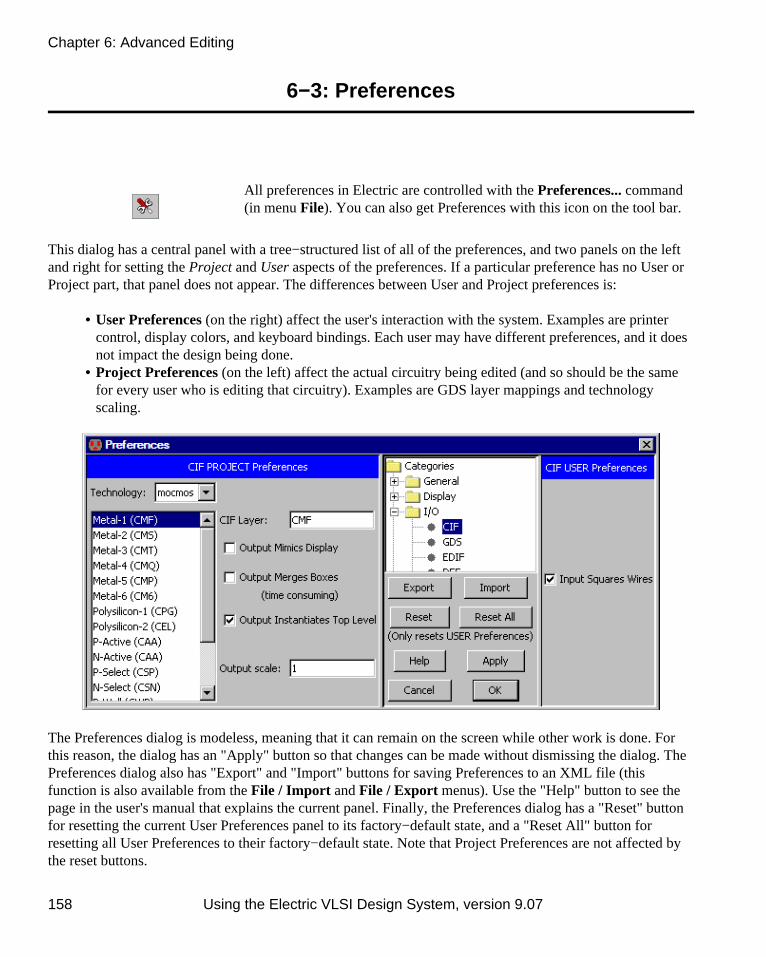
6−3: Preferences
All preferences in Electric are controlled with the Preferences... command(in menu File). You can also get Preferences with this icon on the tool bar.
This dialog has a central panel with a tree−structured list of all of the preferences, and two panels on the leftand right for setting the Project and User aspects of the preferences. If a particular preference has no User orProject part, that panel does not appear. The differences between User and Project preferences is:
User Preferences (on the right) affect the user's interaction with the system. Examples are printercontrol, display colors, and keyboard bindings. Each user may have different preferences, and it doesnot impact the design being done.
•
Project Preferences (on the left) affect the actual circuitry being edited (and so should be the samefor every user who is editing that circuitry). Examples are GDS layer mappings and technologyscaling.
•
The Preferences dialog is modeless, meaning that it can remain on the screen while other work is done. Forthis reason, the dialog has an "Apply" button so that changes can be made without dismissing the dialog. ThePreferences dialog also has "Export" and "Import" buttons for saving Preferences to an XML file (thisfunction is also available from the File / Import and File / Export menus). Use the "Help" button to see thepage in the user's manual that explains the current panel. Finally, the Preferences dialog has a "Reset" buttonfor resetting the current User Preferences panel to its factory−default state, and a "Reset All" button forresetting all User Preferences to their factory−default state. Note that Project Preferences are not affected bythe reset buttons.
Chapter 6: Advanced Editing
158 Using the Electric VLSI Design System, version 9.07

Where Preferences Are Stored
All Preferences are stored permanently on your computer and are remembered each time you run Electric.The actual location of this information varies with each operating system.
Windows: In the registry. Look in: HKEY_CURRENT_USER / Software / JavaSoft / Prefs / com /sun / electric.
•
UNIX/Linux: In your home directory. Look in: ~/.java/.userPrefs/com/sun/electric • Macintosh: In your home directory, under Library/Preferences. Look at:~/Library/Preferences/com.sun.electric.plist
•
You can delete the appropriate data to reset Electric to its "factory" state.
To save your preferences to disk, for saving and transporting to other systems, use the "Export" button in thePreferences dialog, or use the Preferences... commands (in menu File / Export). This will write an XML filewith preference information which can be read back into Electric with the "Import" button, or thePreferences... commands (in menu File / Import).
Project Preferences are also saved with your circuitry so that the values will be correct when the circuits areread back in.
By default, project preferences are saved in each library that is written to disk. However, for multiple−libraryprojects, this can be troublesome if some libraries have different preferences than others. The solution is tocreate a file, in the same directory as the libraries, called "projsettings.xml". If this file exists, thenpreferences are taken from it (and ignored in the libraries). To write this file, use the ProjectPreferences... command (in menu File / Export). To override current settings and explicitly read a projectpreferences file, use the Project Preferences... command (in menu File / Import).
When Electric finds Project Preferences that are inconsistent with the current values, this dialog appears. Youmust choose whether you want to use the new setting values or the current setting. This can be done on anindividual basis, or for all settings that conflict.
Chapter 6: Advanced Editing
Using the Electric VLSI Design System, version 9.07 159

6−4: Making Arrays
If one copy is not enough, Electric has a command for building an array of circuitry.
The Array... command (in menu Edit) takes the currently highlighted objects and replicates them manytimes. You specify the number of replications in the X and Y directions and the geometry is arrayed.Arbitrary expressions can be used in this dialog, for example "3*4+1".
Arrays are generated by X(row) with Y (column),following a raster scanorder. If you request thatalternate rows or columnsbe flipped, then they aremirrored in the directionof repetition. If yourequest that alternate rowsor columns be staggered,then each element is offsetby an alternating amount.If you request that therows or columns becentered, then the originalcircuitry will be placed inthe middle of the arrayinstead of the corner. If theX or Y values arenegative, then the array islaid out backwards(replications are placed inthe reverse direction).
There are four ways to specify spacing: edge overlap, centerline distance, essential bounds spacing, ormeasured distance. The edge overlap amounts indicate the amount by which the rows and columns will besqueezed together (zero overlap causes the each arrayed copy to touch the next one, negative overlap can bespecified to spread the objects apart). Centerline distance is the distance between object centers, and defaultsto the size of the selected objects (which causes the copies to touch). Essential bounds is a size that is set forset for specific cells by placing two or more Essential Bounds nodes in the cell (see Section 7−6−3). If a cellwith essential bounds is arrayed, that value can be used. Finally, the last measured distance can be used todetermine the array spacing (for more on measuring, see Section 4−7−4).
Chapter 6: Advanced Editing
160 Using the Electric VLSI Design System, version 9.07

Checkboxes at the bottom of the dialog are special cases:
"Linear diagonal array" indicates that the array is linear (one of the repeat factors must be 1) but thatboth spacing rules will be applied. This therefore creates a single line that runs diagonally.
•
"Generate array indices" requests that the array entries be drawn with index information. When thisis checked, array entries are labeled with the index of each entry. The original copy is labeled "0−0"and the copy to its right is labeled "1−0". These names are simply visual tags that have no bearing onthe contents (use the Object Properties... command, in menu Edit / Properties, to set or removethese names).
•
"Only place entries that are DRC correct" requests that array entries only be placed where they donot create design−rule violations. This option is only available if a single node is being arrayed. Afterthe array is created, the design−rule checker is run on each entry, and if it causes an error, it isremoved.
•
"Transpose placement ordering" requests that array placement go by column instead of by row. Thisis useful if the arraying includes names which are being auto−incremented in the array. Bytransposing the order of arraying, the names will run in the orthogonal direction.
•
Note that the Array dialog is modeless and can remain on the screen while other work is being done. Both the"OK" and "Apply" buttons create an array, but the "OK" button also closes the dialog. The "Draw" buttonlets you drag an area on the screen in which the array will be placed. As you are dragging the area, theindividual array elements are shown so that you can see the extent of the array. When the button is released,the array is created.
Chapter 6: Advanced Editing
Using the Electric VLSI Design System, version 9.07 161

6−5: Spreading Circuitry
When a large amount of circuitry has been placed too close together or too far apart, Electric's constraintsystem can help. All that is necessary is to make all arcs in an area rigid and then move one node. Of course,you may have to move more than one node if the one you pick is not connected to everything else you wantto move. Also, you must make sure that arcs connecting across the area boundary are nonrigid. Finally,setting arc rigidity should be done temporarily so that it does not spoil an existing constraint setup. All theseoperations are handled for you by the Spread... command (in menu Edit / Move).
With the Spread... command, thehighlighted node is a focal point about whichobjects move. A dialog is presented in whichan amount and a direction (up, down, left, orright) are specified. An infinite line is passedthrough the highlighted node's center andeverything above, below, to the left of, or tothe right of the line is moved by the specifiedamount.
Negative spread distances compact the circuit.
Chapter 6: Advanced Editing
162 Using the Electric VLSI Design System, version 9.07

6−6: Replacing Circuitry
The Change... command (in menu Edit) removes the currently highlighted node or arc and replaces it with anew one of a different type.
This same effect can be hadby copying one object andthen pasting it onto another(see Section 6−1). A dialogis presented in which thepossible replacements areshown. For node changing,you can choose to showprimitives from the currenttechnology, cells from thecurrent library, or both.
When replacing an arc, theexisting nodes on either endmust be able to reconnect tothe new type of arc. If"Change nodes with arcs" ischecked, nodes will bechanged to allow the newtype of arc to remainconnected.
When replacing a node, the existing arcs on it must be able to reconnect properly to the new node. However,the sizes of the replaced object can be different, and the layout will be adjusted. Electric determines whichports on the replaced node to use by examining the port names and locations. If the ports are alignedcorrectly but not named the same, this matching will fail. Check "Ignore port names" to disable namematching and use only position information. If the new node is missing essential ports, such that existingwires cannot be reconnected, then the change will fail (unless "Allow missing ports" is checked).
When replacing schematic icon instances, any parameters that were overridden on the original instance arecopied to the new instance. To prevent this, uncheck "Preserve parameters".
Chapter 6: Advanced Editing
Using the Electric VLSI Design System, version 9.07 163

Besides replacing the currently highlighted node or arc ("Change selected ones only"), it is also possible tospecify replacement of many other objects.
"Change all connected to this" requests that objects of the same type, which are connected to thehighlighted ones, be changed.
•
"Change all in this cell" requests that all objects of the same type in this cell be changed. • "Change all in this library" requests that all objects of the same type in the current library bechanged.
•
"Change all in all libraries" requests that all objects of the same type in every library be changed. •
This is a modeless dialog: it can remain up while other editing is being done. Click "Done" to dismiss it, and"Apply" to make a change.
Note that some Schematic nodes use parameters to further describe them. For example, an electrolyticcapacitor is really just a capacitor with the "electrolytic" parameter on it. Therefore, you can change a nodeinto a capacitor, but not an electrolytic capacitor, because it is not in the list. To change a capacitor into anelectrolytic capacitor, paste an electrolytic capacitor onto it. Besides capacitors, parameters can be found ondiodes, transistors, sources, and two−ports (the four−connection primitives such as VCCS).
Replacing Cell Instances
There are two special commands for working with cell instances. The Replace Instance with DuplicateCell... command (in menu Cell) allows you to modify the selected cell instance, independently of otherinstances of the same cell. It does this by making a copy of the selected cell and changing that instance to usethe new copy. You can then go down the hierarchy and edit that cell without affecting other instances. Thecommand will prompt you to name the new copy of the cell that is being used for the selected instance.
Another command for changing circuitry is Replace Cells from Library... (in menu Cell / MergeLibraries). This command replaces instances in the current cell with like−names ones from another library.It is useful when a new standard−cell library is replacing an old one, and all instances must be switched.
Chapter 6: Advanced Editing
164 Using the Electric VLSI Design System, version 9.07

6−7: Undo Control
Electric has an undo mechanism that tracks all changes made during a session. When a command is issued, itand its side effects are stored.
The Undo command (in menu Edit) reverses the last change made (this includes any changes that may havebeen made by other tools). Multiple uses of the Undo command continue to undo further back. TheRedo command redoes changes, up to the most recent change made.
You can also use the undo (counterclockwise) and redo (clockwise) iconsfrom the tool bar.
Electric stores only the last 40 changes, so anything older than that cannot be undone. To increase thenumber of changes that are saved, use the General Preferences (in menu File / Preferences..., "General"section, "General" tab), and change the "Maximum undo history" field. To see a history of changes that weremade, use the Show Undo List command (in menu Edit).
In Electric, almost every command is undoable, but there are some exceptions. Commands that write diskfiles are not undoable, because Electric would not be so presumptuous as to delete a disk file. Also,commands that read a disk file are undoable, but because users generally do not want to remove librariesfrom memory once read in, the system prompts you to be sure that such a large undo is really desired.
Another useful command in for controlling changes being made is Repeat Last Action (in menu Edit). Thisrepeats the last command, but only works for commands that can sensibly be repeated.
Chapter 6: Advanced Editing
Using the Electric VLSI Design System, version 9.07 165

6−8: Text
6−8−1: Understanding Text
There are a number of ways to place text in a circuit.
Each unexpanded instance of a cell has text that describes it, and its ports. • Each export has a text label. • Nodes and arcs can be named (with Object Properties...) so that they have text on them. They canalso have additional attributes that appear as text. For NCC annotations, see Section 9−7−4. ForSpice multipliers, see Section 9−4−3. For Verilog transistor strength, see Section 9−4−2. For GDStext, see Section 7−3−3.
•
Certain primitive nodes (such as the Flip−Flop component of the Schematic technology) have text asan integral part of their image.
•
It is even possible to create a special node that is only text (with some of the commands under the"Misc" entry of the component menu: "Annotation Text", "Spice Code", "Spice Declaration","Verilog Code", and "Verilog Declaration").
•
Schematic and icon cells can have parameter definitions, and the instances of those cells can haveparameter values (see Section 6−8−5).
•
Essentially, every piece of text on the display is tied to some node or arc (or occasionally a cell). Byunderstanding the relationship between text and its attached object, it becomes easy to manipulate that text.
The visibility of text can be controlled with the "Layers" tab of the sidebar (see Section 4−5−3). This allowsyou to reduce the clutter of text on the display.
When the node or arc that the text is tied to is modified (rotated or mirrored), the text adjusts as well. Thetwo text factors that change are (1) the offset of the text from the center of the node, and (2) the anchor point.
The example here shows therotation of an offpage node thathas an export on the flat end.
The left side of the example shows the node and text before the node is rotated: the export text is anchored onthe right side (the green "U" shows the anchor point, see Section 6−8−2) and the anchor point is offset to theleft of center so that it starts at the left side of the node.
After rotation (on the right) the export text is anchored on top and the anchor is rotated to be below the node.
Note that all other text factors remain unchanged when the attached object is modified. This includes the textrotation, which can be set only in the Properties dialog (see Section 6−8−3).
Chapter 6: Advanced Editing
166 Using the Electric VLSI Design System, version 9.07

6−8−2: Selecting Text
The only category of text that is not selectable is the text that is integral to a node's graphics (i.e. theFlip−Flop). For the rest, you can select and manipulate the text just as you would the object on which the textresides. (Note that port names on cell instances are not selectable: instead, select their export name inside ofthe cell definition.)
Note that the name of an unexpanded cell instance is not easily selectable. This is a feature that preventsaccidental selection of unimportant text. For these hard−to−select pieces of text, the only way to select themis to use special select mode (see section 2−1−5).
All text is attached to its node, arc, orcell at an anchor−point. This is the onepoint on the text that never moves,regardless of the size of the text. Thehighlighting of selected text variesaccording to the anchor−point.Typically, the highlighting consists ofan "X" through the text. This indicatesthat the anchor−point is in the center. Ifa "U" is drawn in any of fourorientations, it indicates that theanchor−point is on the side and that thetext grows out of the opened end. If an"L" is drawn in any of four orientations,it indicates that the anchor−point is in acorner.
Besides these 9 anchor points, there is one more special type of anchor called boxed. Boxed text has acentered anchor point, but is limited in size to a particular box. It appears as an "X" but also has four linesthat indicate the edge of the box. Boxed text is typically used on unexpanded cell instance names so that thetext does not exceed the size of the instance.
Note that text can be moved away from itsattached node or arc. If this has been done, thenselection of the text will also indicate theattached component by drawing a dashed line toit.
Chapter 6: Advanced Editing
Using the Electric VLSI Design System, version 9.07 167

6−8−3: Modifying Text
Like nodes and arcs, text can be moved simply by clicking and dragging. Text can be rotated by selecting itand using the Rotate commands in the Edit menu. Text can be erased by selecting it and using theSelected command of the Edit / Erase menu (the Delete key).
Changing a Single Piece of Text
To change text, double−click on it and type a new value. To change other aspects of selected text, and use theObject Properties... command (in menu Edit / Properties).
Besides the text at the topof the dialog, these fieldscan be modified:
"Text Size" can beabsolute (given in"points") orrelative (given inunits).
•
"X/Y offset" isrelative to thecenter of theattached object.
•
"Rotation" is in90−degreeincrements only.
•
"Anchor" is the point in the text that remains unchanged (see Section 6−8−2).• "Font" can be the default font or any font installed on your system.• "Color" can be any color.• "Bold", "Italic", and "Underline" can be set in any combination.•
These additional factors can be controlled:
"Code" allows the text to be code in an interpretive language, in which case, the evaluation of thatcode is displayed. The code choices are:
•
Chapter 6: Advanced Editing
168 Using the Electric VLSI Design System, version 9.07

"Not Code" the text is taken as−is.♦ "Java" the text is handed to a Java interpreter for evaluation. For example, the expression"Math.abs(−4*5)" will be converted to "20".
♦
"Spice" the text is handled as a Spice expression. Spice allows simple expressions andElectric is able to evaluate them. These expressions are not as powerful as Java. Oneadvantage of Spice code is that the Spice deck writer can send them unevaluated to the Spicedeck.
♦
"Units" can be any electrical type (capacitance, resistance, etc.) See Section 7−2−2 for more on units.• "Show" allows you to show the text value, the name of the piece of text, or both.• "Multi−Line Text" allows the text to have more than one line. After checking this box, it may beuseful to stretch the dialog in order to have a larger field for editing the text.
•
"Highlight Owner" highlights the node or arc on which the text is attached.• "Invisible outside cell" requests that the text not be drawn when an instance of the cell is examined.•
Changing Multiple Pieces of Text
The above dialog changes information on a single piece of text. There are two ways to change information onmultiple pieces of text: (1) select all of the text and use Object Properties... or (2) use the Change TextSize... command (in menu Edit / Text).
The Change TextSize... command allows you tochange the size, font, and styleof any text object. Instead ofselecting the text, you have achoice of 6 classes of text thatcan be changed, and you canchoose whether to make thechanges only on selectedobjects, in the current cell, inall cells of a particular view,or everywhere.
Chapter 6: Advanced Editing
Using the Electric VLSI Design System, version 9.07 169

6−8−4: Text Defaults
To change default information for all new text, use the Text Preferences (in menu File / Preferences...,"Display" section, "Text" tab). The top part of the dialog controls how new text will appear. Select the typeof text, and then its appearance (size, anchor, font, etc.)
The middle section is "For Textual Cells" and controls the fonts used to display textual cells (see Section4−9).
The bottom part ofthe dialog controlstext drawn incircuitry. You canset the default font,and a global textscale for the currentand new windows.Normally, all text isdrawn at 100% ofits stated size.However, you canglobally scale alltext by typing avalue other than 100into this field. Youcan also use theIncrease All TextSize and DecreaseAll TextSize commands (inmenu Edit / Text)to change this value,and alter the size ofall displayed text.
The "Show temporary node names" checkbox requests that unnamed nodes show their temporary names (formore on node names, see Section 2−4−2).
Chapter 6: Advanced Editing
170 Using the Electric VLSI Design System, version 9.07

The Smart Text Preferences (in menu File / Preferences..., "Display" section, "Smart Text" tab) controlswhere new text will appear on Exports and Arcs.
For arcs, you canchoose to place thename on the insideof the arc (thedefault), or on oneside of the arc,depending onwhether it is verticalor horizontal.
For export names,you can control theiroffset relative to thearc attached to thatexport. For example,if a node on the leftend of a wire has anexport, and the"Horizontal"placement is set to"Inside", then theexport text willattach on the leftside, causing thelabel to appearinside of the wire.
Chapter 6: Advanced Editing
Using the Electric VLSI Design System, version 9.07 171

6−8−5: Cell Parameters
Parameters are special pieces of text that are passed from icon instances to the schematic cells. Parametersare defined in the icon or schematic cell, and then they appear on the icon instances. Users can set differentvalues on each icon instance, and these values will be passed down into the schematic and applied asnecessary. The computer−programming equivalent of this is that the cell's parameter is the "formal" valueand the instance parameters are the "actual" values.
For example, an inverter schematic may have transistor sizes defined with a parameter. The actual transistorsinside of the inverter schematic will use the parameter values, and each inverter instance will have a differentparameter value, causing that particular inverter to have a different transistor ratio. Another example of theuse of cell parameters is in the Spice primitives, where user−defined values (such as voltage) arecommunicated into the icon for generation in the Spice deck (see Section 9−4−4).
To define parameters on a cell,it is necessary to be editingeither the schematic or one ofits icons (it does not matterwhich, because the set ofparameters is the same insideof the cell group). Use the CellParameters... command (inmenu Edit / Properties).
A list of parameters is shownat the top. You can create anew parameter by typing itsname in the "Name" field, itsdefault value in the "Value"field and then clicking the"Create New" button. If"Show new parameter oninstances" is checked, this newparameter will be seen on allinstances with its defaultvalue.
Chapter 6: Advanced Editing
172 Using the Electric VLSI Design System, version 9.07

The "Edit" button next to the "Value" field lets you change the value in a separate dialog (useful for majorchanges). You can delete a parameter with the "Delete" button and change its name with the "Rename..."button. You can also copy parameters from another parameterized cell using the "Copy From Cell..." button.
The bottom part of the dialog has controls for the appearance and nature of the selected parameter.
"Code" determines whether the parameter is code or pure data. This can be changed to one of theinterpretive languages in Electric. When this happens, the parameter value is treated as code that issent to that interpreter. Then, the true value of the parameter is the evaluation of that code. Forexample, if the value of a parameter is "3+5" and the parameter is set to be Java code, then the Javainterpreter will be invoked, and the parameter will actually be "8".
•
"Units" determines the type of unit (choices are capacitance, resistance, inductance, current, voltage,or distance). See Section 7−2−2 for more on these units.
•
"Show" controls the way that a parameter is displayed in the circuit. You can request that variouscombinations of the parameter's name and value be displayed.
•
"Text Size" gives the size of the parameter text, which can be in relative or absolute units.• "X/Y offset" is the distance of the text's anchor point from the center of the cell.• "Rotation" is the text orientation (in 90−degree increments).• "Anchor" controls the anchor−point of the parameter text. When the anchor style is "Boxed", the"Boxed width" and "height" fields give the size limits. See Section 6−8−2 for more on text anchors.
•
"Font" is the text font.• "Color" is the text color.• "Bold", "Italic", and "Underline" control the style of the text.• "Invisible outside cell" requests that the parameter not be drawn when viewed farther up thehierarchy.
•
The "Done" button terminates this dialog. Note that there is no "Cancel" button: this dialog makes changes asthey are entered.
Special Considerations
To use a parameter inside of a cell, create text that has the code set to "Java" and has a "@" in front of theparameter name. For example, if a cell has the parameter "size" defined and you want a transistor in the cellto be size*2 in width, then edit the transistor and set its width to "@size*2" and its code to "Java".
To display the current value of a parameter from up the hierarchy, create a piece of "Annotation Text" (foundin the "Misc" entry of the component menu) and set its "code" to Java and its value to "@PNAME" (wherePNAME is the parameter name). Note that when a parameter is used in a cell but there is no value from upthe hierarchy, the text appears as "not found".
Parameters on cells are not tied to any node or arc. Instead, they float freely inside of the cell. You can selectthe text and drag it to any location in the cell.
Parameters get inherited when the cell is instantiated. This means that each new icon, when created, willhave all of the parameters shown on it, with default values. You can select any of these pieces of text and edit
Chapter 6: Advanced Editing
Using the Electric VLSI Design System, version 9.07 173

their text or other information (with the exception of the "Units" field which must match the definedparameter's units). If you delete a parameter's text, the parameter remains, but with its default value.
Parameters on instances of cells are placed at the same location as they appear inside of the icon cell. Tochange the location on all subsequently created icon instances, move the location in the icon.
If a parameter is added to a cell without checking "Show new parameter on instances", existing instances ofthat cell will not show the parameter. To see the parameter at a later time, use the Update Parameters onNode command (in menu Edit / Properties). To do this everywhere, use the Update Parameters allLibraries command.
It is sometimes desirable for each instance parameter to have a unique value. When the default value of aparameter inside the schematic or icon cell has "++" in it, then the number before that will be incrementedafter each new icon instance is created. Similarly, a "−−" indicates that the number be decremented afterinstance is created. This allows all instance parameters to be given unique values.
Chapter 6: Advanced Editing
174 Using the Electric VLSI Design System, version 9.07

6−9: Networks
6−9−1: Introduction to Networks
A collection of electrically connected components defines a network. Networks may span many arcs, or theymay reside on only a single export of a single node. Because networks are stored in the Electric database,they can be immediately accessed when needed.
Whenever a port on a node is selected, the highlighting indicates the entire network that is connected to thatport. Another way to see an entire network is to use the Show Network command (in menu Tools /Network). This will highlight all arcs on the currently selected networks. Repeated use of the commandcauses the network to be highlighted at successively lower levels of the hierarchy, useful when cell instancesare part of the network. The command will also "cross−probe" by highlighting networks that have the samename in other views of this cell.
Cells that are imported from other EDA systems often have no connectivity information and are built withpure layer nodes (see Section 6−10−1 for more). When the Show Network command is run on such cells, itquickly extracts the information, then displays it. Also, if a cell instance is selected but no individual port isselected (such that there is no single network selected) then the command highlights all wired ports.
If the design is very dense, you can select one or more networks by name with the Select Object... command(in menu Edit / Selection). The Show All Networks command (in menu Tools / Network) highlights everynetwork in a different color (useful if there are not too many nets).
There are many commands in the Tool / Network menu that give information about the networks in a cell:
List Networks shows a list of the networks in the current cell. • List Exports on Network lists all export names on the currently highlighted network. This listcontains the names of exports at all levels of the hierarchy, above and below the current cell. Thefacility is useful if, for example, you have propagated clock lines throughout the circuit and wish tomake sure that all of the export names on this network have some variant of the name "phi". Byquickly examining this list, you can see all of the names that have been used on the network,throughout the hierarchy.
•
List Exports below Network lists all export names on the currently highlighted network. This list issimilar to the one generated by List Exports on Network except that it works only on cells belowthe current one.
•
List Connections on Network lists all nodes in the current cell that are connected to the currentnetwork. This list includes only those nodes at the ends of the net, not the pin or contact nodes usedinside of the network. The command is useful if you are at one end of a wire and want to check to seewhat is at the other end.
•
List Geometry on Network lists all geometry in the current cell that is connected to the current•
Chapter 6: Advanced Editing
Using the Electric VLSI Design System, version 9.07 175

network. This reports the area and perimeter of all attached layers. Calculate Network Quality analyzes the currently selected network for length, area, and via usage. • List Total Wire Lengths on All Networks lists the lengths of all networks in the current cell.• Show Undriven Networks lists all networks in the current cell or below it in the hierarchy that are"undriven." An undriven network is one that does not connect to the source or drain of a transistor.
•
6−9−2: Naming Networks
Network names are derived from export names and arcs that are named in a cell. The name given to an exportbecomes the network name for all arcs connected to that export. Similarly, the name given to an arc (bysetting the name field in the Object Properties... dialog) becomes the name of the network for all connectedarcs. You can rename a network by changing the name of a connected export or arc.
Two phenomena can occur in network naming: a network can be multiply named, and it can span disjointcircuitry. A network has multiple names when two or more connected arcs or exports are named withdifferent names. For example, if you make an export on a contact node and call it "clock", then you select anarc connected to that contact node and name it "sig", the circuitry will be on the network "clock/sig." Thus,both names now apply to the same network.
The other phenomenon of network naming is that a single network can include unconnected parts of thecircuit. This happens when arcs in unconnected parts of the circuit are given the same name. This causes thetwo arcs to be implicitly joined into one network. Because this network naming phenomena is mostcommonly used in schematics, the unification of like−named networks only happens in cells with the"schematic" view.
6−9−3: Bus Naming
The Bus arc of the Schematics technology is a special arc that can carry multiple signals (see Section 7−5−1).When giving a network name to Bus arcs, it is possible to specify complex bus names.
Simple arrays Bus names can be arrays (for example, "A[0:7]" which defines an 8−wide bus). Theindices can ascend or descend.
•
Lists Bus names can be lists (for example, "clock,in1,out" which aggregates 3 signals into a 3−widebus).
•
Array index lists and ranges Arrayed bus names can have lists of values (separated by commas) orranges of values (using the colon). For example, the bus "b[0],c[3,5],d[1:2],e[8:6]" is an 8−wide buswith signals in this order: b[0], c[3], c[5], d[1], d[2], e[8], e[7], e[6].
•
Multidimensional array indices Arrays can be multiply indexed (for example "b[1:2][100,102]"defines a bus with 4 entries: b[1][100], b[1][102], b[2][100], and b[2][102]). You can have anynumber of dimensions in an array. Note that the order of signals in a multidimensional array is suchthat the rightmost index varies the fastest. For example, the bus "D[1:2][1:2]" has signals in thisorder: D[1][1], D[1][2], D[2][1], D[2][2].
•
Symbolic array indices It is possible to use symbolic indices in bus naming (for example, the bus"r[x,y]" defines a 2−wide bus with the signals r[x] and r[y]).
•
Chapter 6: Advanced Editing
176 Using the Electric VLSI Design System, version 9.07

When a bus is unnamed, the system determines its width from the ports that it connects. Some tools (such assimulation netlisters) need to name everything, and so use automatically−generated names. When thishappens, the system must choose whether to number the bus ascending or descending. To resolve this issue,use the Network Preferences (in menu File / Preferences..., "Tools" section, "Network" tab), and choose"Ascending" or "Descending". (For information about the "Node Extraction" portion of the NetworkPreferences, see Section 9−10−2.)
Individual wires that connect to a bus must be named with names from that bus. As an aid in obtainingindividual signals from a bus, the Rip Bus command (in menu Edit / Arc) will automatically create suchwires for the selected bus arc.
To find out what signals are on a bus, select that bus and use the Object Properties... command (in the Edit /Properties menu). In the full dialog (obtained by clicking the "More" button), select "List Shows BusMembers" to see a list of networks on the selected bus arc. When a node's port is a bus, you can see thesignals on that bus by selecting that port of the node and using the Object Properties... command. In the fulldialog, select "Bus Members on Port" to see the signals.
Chapter 6: Advanced Editing
Using the Electric VLSI Design System, version 9.07 177

Arrayed Nodes
Besides using array names on busses, you can also give array names to cell instances in a schematic.Netlisters will create multiple copies of that node, named with the individual elements of the array.
When a cell instanceis arrayed, theconnections to itsports can be similarlyarrayed. For example,suppose thatschematic cell X haswire port Y and busport Z[1:2]. Aninstance of cell X isarrayed by giving itthe name M[2:4].Ports Y and Z can beconnected in twoways:
Implicit connection to all instances (top illustration). If the wire port Y is connected to a single wire(A), then wire A connects to port Y on all three instances of cell X. If the bus port Z is connected to a2−wide bus (B), then each element of that bus connects to the same element of bus port Z on all threeinstances of cell X. So B[1] connects to port Z[1] and B[2] connects to Z[2] on all three instances,M[2], M[3], and M[4].
•
Explicit connection to individual instances (bottom illustration). If the wire port Y is connected to a3−wide bus (C), then each element of the bus connects to port Y on a different instance of cell X.C[1] connects to Y on M[2]; C[2] connects to Y on M[3]; and C[3] connects to Y on M[4]. If the busport Z is connected to a 6−wide bus (D), then it is viewed as 3 pairs of signals, and each pairconnecting to the two−wide bus Z on a different instance of cell X. D[1] and D[2] connect to Z[1]and Z[2] on M[2]; D[3] and D[4] connect to Z[1] and Z[2] on M[3]; and D[5] and D[6] connect toZ[1] and Z[2] on M[4].
•
Note that it is not possible to array a primitive node from the Schematic technology. Instead, you must placethat node inside of a cell, and array instances of the cell.
Chapter 6: Advanced Editing
178 Using the Electric VLSI Design System, version 9.07

Parameterized Bus Names
It is possible to have variable−widthbusses by parameterizing their names.Electric maintains a list of globalparameters, and these can bemanipulated with the Edit BusParameters... command (in menu Edit/ Properties). You can create and deleteparameters, and can set values for each.
To use these parameters, you must add a template to an arc, node, or export name.
This figure shows anexport called "in", and anarc called "internal". Boththe export name and the arcname were selected, andthe commandParameterize BusName issued (in menuEdit / Properties).
The templates are then shown near the original names. Arrayed nodes can also have their namesparameterized.
You may type any text into the template. Wherever the string $(par) appears, it will be replaced with theparameter par. In this example, the parameter x has the value 7. You can also use simple arithmeticoperators (just "+", "−", "*", and "/"), for example in[0:$(x)−1] defines a bus that runs from 0 to oneminus the value of "x". When parameter values change, click the "Update All Templates" button toreevaluate all node, arc, and export names.
Chapter 6: Advanced Editing
Using the Electric VLSI Design System, version 9.07 179

6−9−4: Power and Ground
Identification of a power network is done by finding:
a Power node from the Schematic technology; • an export in the current cell that has the "power" characteristic; • an export in the current cell that begins with the letters "vdd", "vcc", "pwr", or "power"; • a port on a component in the current cell that has either of the above two properties. •
Ground networks use the same rules, except that the acceptable port names begin with "vss", "gnd", or"ground".
All supply networks defined with the Power and Ground nodes of the Schematic technology are combinedinto one network. This means, for example, that two arcs, each connected to a separate Ground node, appearon the same network regardless of their actual connectivity in the circuit.
As a debugging aid for power and ground networks, the command Show Power and Ground (in menuTools / Network) shows the entire power and ground network. The Validate Power and Ground commandchecks all power and ground networks in the circuit. Any power or ground networks that are namedaccording to the prefixes listed above must have the proper characteristics. If, for example, a power networkis called "gnd007", then it will be flagged by this command. The command Repair Power andGround changes the characteristics where necessary.
Many designs require multiple power and ground rails. Electric allows additional power and ground signalsthrough the use of the Global node (see next Section).
6−9−5: Global Networks
When wiring an IC layout, the only way to get a signal from one point to another is to physically place thewires. Signals that span a large circuit, such as power and ground, must be carefully wired together at eachlevel of the hierarchy.
In schematics, however, it is often the case that a signal is used commonly without explicitly being wired orexported. Examples of such signals are power, ground, clocks, etc. The power and ground signals can beestablished in any schematic with the use of the Power and Ground nodes. To create another such signal, usethe Global node of the schematics technology (see Section 7−5−1).
The Global node is diamond−shaped, and it has a name and characteristic similar to exports (input, output,etc.) All signals with the same global name are considered to be connected when netlisting occurs. Thus, theGlobal symbol can be used to route clock signals, as well as to define multiple power and ground rails. Notethat with multiple power and ground rails, only one of them is the true "power and ground" as defined by thePower and Ground symbols. All others, declared with Global nodes, are not true power and ground signals,but are simply globals. The distinction is made by some netlisters which treat the true power and groundsignals specially.
Chapter 6: Advanced Editing
180 Using the Electric VLSI Design System, version 9.07

Global Partitioning
It is sometimes the case that the designer wishes to isolate a global signal and wire it differently. Forexample, a schematic cell may be defined with power and ground symbols, connecting it to the global powerand ground. But a particular instance of the cell may need to be wired to alternate power and ground rails, forexample "dirty power". Another example of rewiring happens when you want to test a specific instance of acell, and you need to connect its globals differently for the purposes of simulation.
The solution is to place a"Global Partition" node insideof the schematic (see Section7−5−1). This symbol acts likean "offpage" symbol: it iswired to something inside ofthe cell (a global signal) and itis also exported to the outsideworld.
In this example, the schematic has power and ground signals, but the power signal is also connected to aGlobal Partition node and exported (as "vddR"). The icon has an extra connection for this power tap. Innormal use, the extra connections created by the Global Partition nodes are not wired up, because theyconnect to globals, and their connectivity is understood. If, however, the extra exports are wired, it meansthat the signal inside of the cell is disconnected from the global, and connected instead to that wire.
In the example here, two "invR" iconsare placed, but only one of them hasits "vddR" connection wired (to adifferent power source). Thesubcircuit for the rightmost icon willnot use the global power signal, butwill instead use the attached signal,"vddInv".
When writing a Spice netlist that makes use of Global Partitions, you cannot use the .GLOBAL blockbecause it will prevent the overriding of signals. You must set the "Globals" field in Spice/CDL Preferencesto "Create .SUBCKT ports" (see Section 9−4−3).
Chapter 6: Advanced Editing
Using the Electric VLSI Design System, version 9.07 181

6−10: Outlines
6−10−1: Introduction to Outlines
For some primitive nodes, it is not enough to rotate,mirror, and scale. These primitives can to beaugmented with an outline, which is a polygonaldescription.
There are quite a few primitive nodes that make useof outline information. The MOS transistors use theoutline to define the gate path in serpentineconfigurations (see Section 7−4−1). The Artworktechnology has nodes that use outline information:Opened−Solid−Polygon, Opened−Dotted−Polygon,Opened−Dashed−Polygon,Opened−Thicker−Polygon, Closed−Polygon,Filled−Polygon, and Spline (see Section 7−6−1).
For arbitrary shapes on arbitrary layers, use thepure−layer nodes in the IC layout technologies. Thepure−layer nodes are found under the "Pure" entry inthe component menu. For example, the node called"Metal−1−Node" in the CMOS technologies lookslike a rectangle of the Metal−1, until you add outlineinformation. With an outline, this node can take anyshape. It is even possible to have multiple disjointoutlines in a single pure−layer node (users cannotcreate this situation, but some tools such as GDSimport can).
Because pure−layer nodes are unusual, it is useful to be able to identify them. Use the Show Pure LayerNodes command (in menu Edit / Cleanup Cell) to highlight all of them in the current cell. If pure−layernodes overlap each other, use Show Redundant Pure Layer Nodes to identify those that are enclosed byothers and, therefore, are redundant.
Chapter 6: Advanced Editing
182 Using the Electric VLSI Design System, version 9.07

6−10−2: Manipulating Outlines
To manipulate outline information on the currently highlighted node, use"Outline Edit" mode (click on the icon in the tool bar or use the ToggleOutline Edit command, in menu Edit / Modes / Edit).
In this mode, there is always a "current point", identified with an "X" over it. To further identify this point,the lines coming into and out of the point have arrows on them indicating the direction of the outline.
In outline edit mode, the left button is used to select and move a point on the outline, and the right buttonadds a new point after the selected one.
Besides selecting points with the mouse, you can also step through the points of the outline with the "." key(next outline point) and "," key (previous outline point). These keys are under the ">" and "keys, so you canthink of them as the "next point" (>) and "previous point" (<) commands.
The Selected command (in menu Edit / Erase) deletes the current outline point (this is the Delete key).
When the Object Properties... command isissued in outline−edit mode, a special dialogappears to show the point coordinates of theoutline.
When done editing the outline, switch to standard selection mode (the Click/Zoom/Wire command, in menuEdit / Modes / Edit).
Chapter 6: Advanced Editing
Using the Electric VLSI Design System, version 9.07 183

6−10−3: Special Outline Generation
To generate a doughnut shaped outline, use the"Annular Ring..." command under the "Misc"entry in the component menu. This dialogprompts for a layer to use and an inner andouter radius for the annulus. By default, it ismade as a full circle (360 degrees), but this canalso be changed. Also, the number of linesegments used in the construction can be set,allowing for smoother or coarser shapes.
Chapter 6: Advanced Editing
184 Using the Electric VLSI Design System, version 9.07

To generate text−shaped outlines, use the "LayoutText..." command under the "Misc" entry in thecomponent menu. This dialog prompts for text and alayer to use as well as the size, scale, font, and style. Anonzero dot separation causes each pixel of the text tobe placed separately (some design rules need this)."Reverse Video" inverts the placement of the dots thatmake up the text.
To generate images in layout, use the"Layout Image..." command under the"Misc" entry in the component menu.This dialog prompts for an image fileand a layer to use as well as otherfactors in generating the image.
Chapter 6: Advanced Editing
Using the Electric VLSI Design System, version 9.07 185

6−11: Interpretive Languages
Electric has two scripting languages: Java (using the Bean Shell) and Python (using Jython). These languagesenable you to load custom code that adds functionality to Electric. Neither of these languages is part of thedefault Electric distribution. You must add them as "plug ins" (see Section 1−5 for more on plug−ins).
To run a Java script, use the Run Java Bean Shell Script... command (in menu Tools / Languages). To runa Python script, use the Run Jython Script... command. Note that during execution of these scripts, Electricmay give warning messages about preferences, which can be ignored.
You can attach a script to theTools / Languages menu byusing the ManageScripts... command. Scriptscan have mnemonic lettersassigned to them (see Section1−9 for more on mnemonics).
Java Script Examples
Here are some example scripts in the Java Bean Shell. For more information about accessing the internals ofElectric, read the Javadoc in the source code.
import com.sun.electric.database.hierarchy.Cell;import com.sun.electric.database.topology.NodeInst;import com.sun.electric.tool.Job;import java.util.Iterator;
// get the current cellCell c = Job.getUserInterface().getCurrentCell();
// find all transistorsfor(Iterator it = c.getNodes(); it.hasNext(); ) { NodeInst ni = it.next(); if (ni.getFunction().isTransistor()) System.out.println("Found transistor: " + ni.describe(false));}
// find all exports that start with "A"for(Iterator it = c.getPorts(); it.hasNext(); ) { com.sun.electric.database.hierarchy.Export e =(com.sun.electric.database.hierarchy.Export)it.next(); if (e.getName().toLowerCase().startsWith("a")) System.out.println("Found export: " + e.getName());}
This example searches thecurrent cell, printing alltransistors and all exportsthat start with the letter"a".
Notice that Electric's"Export" object must be afully−qualified name,because the name"Export" is used for otherreasons in the Bean Shell.This also applies toElectric's "EPoint" class.
Chapter 6: Advanced Editing
186 Using the Electric VLSI Design System, version 9.07

import com.sun.electric.database.hierarchy.Cell;import com.sun.electric.database.topology.NodeInst;import com.sun.electric.technology.PrimitiveNode;import com.sun.electric.technology.Technology;import com.sun.electric.tool.lang.EvalJavaBsh;import java.awt.geom.Point2D;
Cell newCell = Cell.makeInstance(Library.getCurrent(), "samp1{lay}");Technology tech = Technology.findTechnology("mocmos");PrimitiveNode trP = tech.findNodeProto("P−Transistor");NodeInst tP = NodeInst.makeInstance(trP, new Point2D.Double(10, 10), trP.getDefWidth(), trP.getDefHeight(), newCell);EvalJavaBsh.displayCell(newCell);
This example createsa new cell, places atransistor in it, anddisplays the cell.
import com.sun.electric.database.hierarchy.Cell;import com.sun.electric.database.geometry.Orientation;import com.sun.electric.database.topology.ArcInst;import com.sun.electric.database.topology.NodeInst;import com.sun.electric.technology.ArcProto;import com.sun.electric.technology.PrimitiveNode;import com.sun.electric.technology.Technology;import java.awt.geom.Point2D;
// create the new cellCell newCell = Cell.makeInstance(Library.getCurrent(), "samp2{lay}");
Technology tech = Technology.findTechnology("mocmos");
// place a rotated transistorPrimitiveNode trP = tech.findNodeProto("P−Transistor");NodeInst tP = NodeInst.makeInstance(trP, new Point2D.Double(0, 20), trP.getDefWidth(), trP.getDefHeight(), newCell, Orientation.R, "T1");
// place a metal−Active contactPrimitiveNode coP = tech.findNodeProto("Metal−1−P−Active−Con");NodeInst maP = NodeInst.makeInstance(coP, new Point2D.Double(8, 20), coP.getDefWidth(), coP.getDefHeight(), newCell);
// wire the transistor to the contactArcProto aP = tech.findArcProto("P−Active");ArcInst.makeInstance(aP, tP.findPortInst("diff−bottom"), maP.findPortInst("metal−1−p−act"));
// export the contactcom.sun.electric.database.hierarchy.Export.newInstance(newCell, maP.findPortInst("metal−1−p−act"), "IN", PortCharacteristic.IN);
This example goes abit further: it createsa rotated transistorand a contact, wiresthem together, andexports the contact.The transistor isnamed "T1."
Chapter 6: Advanced Editing
Using the Electric VLSI Design System, version 9.07 187

Python Script Examples
from com.sun.electric.database.hierarchy import Cellfrom com.sun.electric.database.topology import NodeInstfrom com.sun.electric.tool import Jobfrom java.util import Iterator
# get the current cellc = Job.getUserInterface().getCurrentCell()
# find all transistorsit = c.getNodes()while it.hasNext(): ni = it.next() if ni.getFunction().isTransistor(): print "Found transistor: " + ni.describe(0)
# find all exports that start with "A"it = c.getPorts()while it.hasNext(): e = it.next() if e.getName().lower().startswith("a"): print "Found export: " + e.getName()
This examplesearches the currentcell, printing alltransistors and allexports that startwith the letter "a".
from com.sun.electric.database.hierarchy import Cellfrom com.sun.electric.database.hierarchy import Libraryfrom com.sun.electric.database.topology import NodeInstfrom com.sun.electric.technology import Technologyfrom com.sun.electric.tool.lang import EvalJythonfrom java.awt.geom import Point2DnewCell = Cell.makeInstance(Library.getCurrent(), "sample1{lay}")tech = Technology.findTechnology("mocmos")trP = tech.findNodeProto("P−Transistor")tP = NodeInst.makeInstance(trP, Point2D.Double(10, 10), trP.getDefWidth(),trP.getDefHeight(), newCell)EvalJython.displayCell(newCell)
This example createsa new cell, places atransistor in it, anddisplays the cell.
Chapter 6: Advanced Editing
188 Using the Electric VLSI Design System, version 9.07

from com.sun.electric.database.geometry import Orientationfrom com.sun.electric.database.hierarchy import Cellfrom com.sun.electric.database.hierarchy import Libraryfrom com.sun.electric.database.hierarchy import Exportfrom com.sun.electric.database.prototype import PortCharacteristicfrom com.sun.electric.database.topology import ArcInstfrom com.sun.electric.database.topology import NodeInstfrom com.sun.electric.technology import Technologyfrom java.awt.geom import Point2D
# create the new cellnewCell = Cell.makeInstance(Library.getCurrent(), "sample2{lay}")
tech = Technology.findTechnology("mocmos")
# place a rotated transistortrP = tech.findNodeProto("P−Transistor")tP = NodeInst.makeInstance(trP, Point2D.Double(0, 20), trP.getDefWidth(),trP.getDefHeight(), newCell, Orientation.R, "T1")
# place a metal−Active contactcoP = tech.findNodeProto("Metal−1−P−Active−Con")maP = NodeInst.makeInstance(coP, Point2D.Double(8, 20), coP.getDefWidth(),coP.getDefHeight(), newCell)
# wire the transistor to the contactaP = tech.findArcProto("P−Active")ArcInst.makeInstance(aP, tP.findPortInst("diff−bottom"),maP.findPortInst("metal−1−p−act"))
# export the contactExport.newInstance(newCell, maP.findPortInst("metal−1−p−act"), "IN",PortCharacteristic.IN)
This example goes abit further: it createsa rotated transistorand a contact, wiresthem together, andexports the contact.The transistor isnamed "T1."
Chapter 6: Advanced Editing
Using the Electric VLSI Design System, version 9.07 189

6−12: Project Management
The project management system in Electric allows multiple users to work together on the design of a circuit.This is accomplished by having a repository in a shared location, and local libraries in each user's disk area.Users work on cells by checking them out of the repository, making changes, and then checking them backin. The project management system ensures that only one user can access a cell at a time. In addition, it alsoapplies its understanding of the circuit hierarchy to inform users of potential inconsistencies that may arise.
The project management system uses the full power of cell naming to accomplish its task. It handles designhistory by creating a new version of a cell each time it is checked out of the repository. The user's librarycontains only the most recent version of each cell, taken from the repository. When a user updates theirlibrary from the repository, newer versions are brought in and substituted for older versions. Unless the userspecifically asks for an older version, it is removed from their library.
Because the project management system uses versions to manage design progress, users are discouragedfrom managing versions explicitly. Thus, the command New Version of Current Cell (in menu Cell) is notallowed. Also, it is not appropriate for a user to use two different versions of a cell explicitly, because theyare considered to be part of a single cell's history.
All commands to the project management system can be found under the Project Management command(in menu File).
Subcommands exist for checking cells in and out, updating local libraries from the repository, and more.Many project management functions are also in context menus in the cell explorer.
Chapter 6: Advanced Editing
190 Using the Electric VLSI Design System, version 9.07

The first step needed to use the project management system is to choose a location for the repository. Thismust be a shared location that each user can access (read and write).
Use the Project Management Preferences, in menu File / Preferences..., "General" section, "ProjectManagement" tab.
Each user must set the same location in their Project Management Preferences so that they can share therepository. Also, be sure that your user name is correct, as this will be used when tagging file changes.
After the repository has been set, libraries can be entered into it. Use the Add Current Library ToRepository command to place your library in the repository. Use Add All Libraries To Repository to addall libraries in the system. Note that a library that has been entered into the repository is also tagged withinformation about the repository location, as well as the state of the cells (checked−in or checked−out).Therefore, you should save your library after entering it into the repository.
Other users can obtain a copy of your library directly from the repository by using the Get Library FromRepository... command.
Checking Cells In and Out
When a cell is not checked out, you cannot make changes to it. Any change is immediately undone by theproject management system. This means that a change which affects unchecked−out cells, higher up thehierarchy, will also be disallowed.
To check−out the current cell, use the Check Out This Cell command. If there are related cells(hierarchically above or below this) that are already checked−out to other users, you will be given warningsabout potential conflicts that may arise.
To check the current cell back in, use the Check In This Cell... command. You will be prompted for adocumentation message about the change. No further changes will be allowed to the cell. Note that whenchecking−in a cell, other cells above and below this in the hierarchy will also be checked−in. This is becausechanges affect other cells in the hierarchy, and so consistent pieces of the hierarchy must be updated at thesame time.
Chapter 6: Advanced Editing
Using the Electric VLSI Design System, version 9.07 191

The cell explorer showsthe state of cells that areunder projectmanagement control (seeSection 4−5−2). Locksare drawn over cells toindicate their state(checked−in,checked−out to you, orchecked−out to others).You can also access manyof the projectmanagement commandsby selecting cells in theexplorer and usingcontext menu commands.
To update your library so that it contains the most recent version of every cell, use the Update command.This will retrieve the newest version of every cell in every library that is being managed. You will be given alist of cells that were replaced.
Advanced Commands
If, after a cell has been checked−out, you change your mind and do not wish to make changes, use theRollback and Release Check−Out command (or use the "Rollback and Release Check−Out" context menuwhen clicking on a cell name in the cell explorer). This will destroy any changes made to the cell since it waschecked−out and revert the cell to its state when it was checked−in.
If, in the course of design, a new cell is created, it must be added to the repository so that others can share it.Use the Add This Cell command to include the cell in the repository. Similarly, if a cell is to be deleted, usethe Remove This Cell command to delete it from the repository.
To examine the history of changes to a cell, use the Show History of This Cell... command (or use the"Show History of This Cell..." context menu when clicking on a cell name in the cell explorer). Besidesshowing the history of changes, you can use this dialog to retrieve an earlier version of the cell.
Chapter 6: Advanced Editing
192 Using the Electric VLSI Design System, version 9.07

Under the Hood
The project management system makes use of version information on all cells to control cell changes. Whena cell is checked−out, a new version is made in your local library, and the old version is deleted. All instancesof the old version are switched to the new version. The old version remains in the repository. When the cell ischecked−in, that new version also goes into the repository. When updates are done, newer versions areobtained from the repository, and appropriate substitutions are performed.
Chapter 6: Advanced Editing
Using the Electric VLSI Design System, version 9.07 193

6−13: CVS Project Management
Electric implements an interface to the Concurrent Versioning System (CVS) program, a popular versioncontrol system. This section assumes the user is familiar with how CVS works, and the various CVScommands. Such information is readily available on the web.
To enable Electric to useCVS, you must firstconfigure the CVSPreferences (in File /Preferences..., "General"section, "CVS" tab). CVSmust be enabled, and therepository location must bespecified. Electric does notimplement the CVSprotocol, it merely providesan interface to interact withan external CVS program,so that program must bespecified in the preferences.
The Electric GUI allows the user to perform the common CVS commands via the menu File / CVS, or viathe popup−context menu on the libraries and cells listed in the explorer tree. The menu commands apply toall libraries; the explorer−tree context menus apply only to the selected library.
With CVS enabled in Electric, the explorer tree uses colors to show the state of libraries or cells in CVS.When using a JELIB or ELIB library format, the library name and all cells are the same color, because theentire library is a single file. When using a DELIB format, the cells are different color, because each cell isits own file. The colors and their associated state are shown below. Colors at the top of the table will bedisplayed before colors at the bottom of the table, if two states are simultaneously valid.
Chapter 6: Advanced Editing
194 Using the Electric VLSI Design System, version 9.07

State Color
Conflicts with CVS version Red
Locally Modified Blue
Needs Update Magenta
Added/Removed Green
Unknown (not in CVS) Light gray
Up−to−date Black
These are the commands implemented by Electric:
Commit Commit a locally modified version to CVS.• Update Retrieves latest version from CVS repository.• Get Status Check the status with respect to the CVS version.• List Editors List other users who have a locally modified version of the file.• Show Log Display a dialog of all versions of the file in CVS (allows checkout of specific version).• Rollback Revert to latest CVS version.• Add to CVS Add the file to CVS (requires a commit to actually add it).• Remove from CVS Remove the file from CVS (requires a commit to actually remove it).• Undo CVS Add or Remove Undo a previous CVS add or remove before a commit is done.• Rollforward Move local modified file to a temporary location, get a fresh copy from CVS and putback the local copy. This is to prevent merge cases with conflicts and still preserve localmodifications.
•
Chapter 6: Advanced Editing
Using the Electric VLSI Design System, version 9.07 195

6−14: Emergencies
Electric uses separate Java threads for all activities. Because of this, if the system encounters an error, itaborts the thread but the main program continues to run.
If a thread crashes and leaves a Job running, then you will not be able to issue other commands, because theirJobs will be queued behind the stuck one (see Section 4−5−2 for more viewing Jobs). Even theQuit command is a job, and so it cannot run. To solve this problem, use the Force Quit (andSave) command (in menu File).
If you suspect that the database is corrupt, use the subcommands of the Check Libraries command (in menuFile). The Check command examines the database but does not fix errors. The Repair command checks andrepairs the database (if it can).
Chapter 6: Advanced Editing
196 Using the Electric VLSI Design System, version 9.07

Chapter 7: Technologies
7−1: Introduction to Technologies
7−1−1: Technologies
A technology is an environment in which design is done. Technologies can be layout specific, for exampleMOSIS CMOS, or they can be abstract, for example Schematics and Artwork. There are multiple CMOSvariations to handle popular design rules such as MOSIS, submicron, etc.
Each technology consists of a set of primitive nodes and arcs. These, in turn, are constructed from one ormore layers. Each technology also includes information necessary to do design, such as design rules,connectivity rules, simulation information, etc.
The primitive nodes in a technology come in three styles:
PINS are used to join arcs, so there is one pin for every arc in the technology. • COMPONENTS are the basic nodes used in design: contacts, transistors, etc. • PURE−LAYER NODES are used for geometric manipulation (see Section 6−10−1). There is onepure−layer node for every layer in the technology.
•
The component menu in the side bar (on the left side of the editing window) shows arcs on the left (the menuentries with red border), pin nodes in the center column (these appear as boxes with a cross inside), andcomponents on the right (the more complex layer combinations). See Section 4−5−1 for more on thecomponent menu.
These are the technologies that come with Electric. Some of these technologies are illustrated with samplecells in the built−in "sample" library. To access this library, use the Load Sample Cells Library command(in menu Help).
artwork is used for drawing graphics, for example when designing icons. See Section 7−6−1 formore. The cell tech−Artwork in the sample library illustrates this technology.
•
bicmos a hybrid bipolar/CMOS technology, as specified by MOSIS using older N−Well SCE rules.• bipolar a bipolar technology (self−aligned, single−poly). The cell tech−Bipolar{lay} in thesample library illustrates this technology.
•
cmos a generic CMOS technology described in a old paper (Griswold, Thomas W., "Portable DesignRules for Bulk CMOS," VLSI Design, III:5, 62−67, September/October 1982). It was never alignedwith an actual process and exists only for illustration.
•
efido a high−level digital−filter architecture technology. The cell tech−DigitalFilter in thesample library illustrates this technology.
•
Using the Electric VLSI Design System, version 9.07 197
fpga a customizable technology that can describe field−programmable gate array architectures. Thebasic technology does not have any FPGA capabilities: it must be customized with a specialarchitecture file (see Section 7−6−2 for more).
•
gem a temporal−logic technology that illustrates Electric's capability to do graph editing innonelectrical environments. Based on the paper: Lansky, A. L. and Owicki, S. S., "GEM: A Tool forConcurrency Specification and Verification," Proceedings 2nd Annual ACM Symposium onPrinciples of Distributed Computing, 198−212, August 1983. The cell tech−Gem in the samplelibrary illustrates this technology.
•
generic a technology used for special features such as inter−technology connections, routingspecifications, cell definitions, etc. This technology is never used for actual design, but its nodes andarcs appear in many places. See Section 7−6−3 for more.
•
mocmos a CMOS technology that conforms to MOSIS design rules. This is the most used CMOStechnology in Electric, because it is kept current with MOSIS rules. See Section 7−4−2 for more. Thecell tech−MOSISCMOS{lay} in the sample library illustrates this technology.
•
mocmosold an older version of the "mocmos" technology, kept for compatibility with older designs.The technology should not be used for any new designs.
•
mocmossub an older version of the "mocmos" technology that focuses on submicron facilities. Thetechnology should not be used for any new designs because the "mocmos" technology incorporatesthese submicron features.
•
mocmos−cn a modified version of the "mocmos" technology that has carbon−nanotube transistors.• nmos an old nMOS technology, based on the book: Mead, C. and Conway, L., Introduction to VLSISystems, Addison−Wesley, Reading, Massachusetts, 1980. The cell tech−nMOS{lay} in thesample library illustrates this technology.
•
pcb a printed−circuit board technology with 8 layers. The cell tech−PCB{sch} in the samplelibrary illustrates this technology.
•
photonics a simple photonics technology with a few basic light−guide elements. The cells namedtech−photonics*{lay} in the sample library illustrate this technology.
•
rcmos a round CMOS technology, based on work at CalTech. The celltech−RoundCMOS{lay} in the sample library illustrates this technology.
•
schematic a schematic capture facility. See Section 7−5−1 for more. The cellstech−SchematicsDigital{sch} and tech−SchematicsAnalog{sch} in the samplelibrary illustrates the digital and analog capabilities of this technology.
•
tft an organic thin−film technology. Thin film transistors are p−type depletion devices formed withan aluminum gate, gold source/drain electrodes, and a pentacene active area. Two layers of metal areavailable for routing signals, Metal−1 (the aluminum gate metal) and Metal−2 (the source/drainmetal). A capacitor is also available in the process and is formed between the gate electrode and asource/drain electrode. The cell tech−TFTInverter{lay} in the sample library illustrates thistechnology.
•
Chapter 7: Technologies
198 Using the Electric VLSI Design System, version 9.07

7−1−2: Controlling Technologies
Electric has the concept of a current technology which is shown in the status bar. This technology affectsmany things, including the selection of nodes and arcs in the component menu. There are a number of waysto affect the current technology, both manual and automatic.
You can change the current technology by selecting it from the popup at the top of the side bar (either the"Components" or "Layers" tab). Electric automatically switches the current technology to match the cellbeing edited. If there are multiple cells being edited from different technologies, this switching can becomeannoying. To disable automatic technology switching, use the Nodes Preferences (in menu File /Preferences..., "General" section, "Nodes" tab), and uncheck "Switch technology to match current cell".
To see a list of primitive nodes and arcs in the current technology, use the Describe thisTechnology command (in menu Edit / Technology Specific). To see a detailed description of the currenttechnology, use the Document Current Technology command.
Some technologies have preferences that further customize them. The Technology Preferences command (inmenu File / Preferences..., "Technology" section, "Technology" tab) lets you control many User and Projectpreferences. The Project Preferences are on the left, and the bottom part of the Project Preferences is specificto the MOSIS CMOS technology. More information about this can be found in Section 7−4−2.
Chapter 7: Technologies
Using the Electric VLSI Design System, version 9.07 199

The Defaults section at the top of the Project Preferences section has these controls:
"Startup technology" controls the technology that is used when Electric first begins. It is also usedwhen reading old libraries that are missing some technology information.
•
"Layout technology to use for Schematics" sets the technology to use for real geometry (anintegrated circuit technology, not a schematics or artwork technology). The default layout technologyis used to give further information about schematics components (see, for example, Section 9−4−3).
•
"PSubstrate process in Layout Technology" declares that the layout technologies use P Substrate(NWell), and therefore the PWell spacing and minimum width rules should be ignored by thedesign−rule checker. Since Electric displays both wells, users might be concerned with filling innotches in the PWell, but in these processes it is not necessary.
•
The User Preferences section is discussed elsewhere For information about rotating transistors in the menus,see Section 7−4−2. For information about Schematic primitive names, see Section 7−5−1 and Section3−11−2.
Chapter 7: Technologies
200 Using the Electric VLSI Design System, version 9.07

7−2: Scaling and Units
7−2−1: Scale
Electric represents all distances in dimensionless units. A transistor that is 2 x 3 in size is actually stored inmemory as 2 x 3. To convert these units to real distances, each technology has a scale, measured innanometers (billionths of a meter). The scale of a technology is shown in the status area after the technology'sname.
For example, if the scale for the MOSIS CMOS ("mocmos") technology is 200 nanometers, then a 2 x 3transistor is actually 400 x 600 nanometers (or 0.4 x 0.6 microns).
To set the scale, usethe ScalePreferences (in menuFile / Preferences...,"Technology section,"Scale" tab).
Scale only applies tointegrated−circuitlayout technologies.There is no scale forSchematics,Artwork, and othernonlayouttechnologies.
Chapter 7: Technologies
Using the Electric VLSI Design System, version 9.07 201

7−2−2: Units
By default, distances areexpressed in dimensionless"grid units", and the true unitsize is shown in the status bar.The Units Preferences (in menuFile / Preferences...,"Technology" section, "Units"tab) allows you to request thatdimensions be shown in realunits, such as nanometers.
You can also control the precision of displayed numbers by setting the number of digits to the right of thedecimal point. This will be used on the display and in netlists.
Chapter 7: Technologies
202 Using the Electric VLSI Design System, version 9.07

7−3: I/O Control
7−3−1: Introduction to I/O Control
Electric is able to read and write circuits in a number of different formats. This is done with the Import andthe Export commands (in menu File). See Section 3−9−2 for more on Import; see Section 3−9−3 for moreon Export.
To properly control translation, use the many Preferences dialogs for the different file types, (in menu File /Preferences..., "I/O" section).
Unfortunately, many of these formats are pure geometry with no information about the circuit connections.When read, they appear as pure−layer nodes. This means that transistors, contacts, and other multi−layernodes are not constructed properly. Although the cell appears visually correct, and can be used to export thesame type of file, it cannot be analyzed at a circuit level. The node extractor can be used to convert thesepure−layer nodes to true Electric components (see Section 9−10−2).
The next few sections describe control of different I/O formats.
7−3−2: CIF Control
CIF (Caltech Intermediate Format) is used as an interchange between design systems and fabricationfacilities. Control of CIF I/O is done with the CIF Preferences (in menu File / Preferences..., "I/O" section,"CIF" tab).
Chapter 7: Technologies
Using the Electric VLSI Design System, version 9.07 203

Project Preferences
The CIF Project Preferences let you can assign CIF names to each layer in the technology. It also offers thesecontrols:
"Output Mimics Display" lets you use CIF output for printing. By default, CIF output writes theentire hierarchy below the current cell. If you check this box, cell instances that are unexpanded willbe represented as an outline in the CIF file. This is useful when the CIF output is intended forhardcopy display, and only the screen content is desired.
•
"Output Merges Boxes" controls the aggregation of geometry when writing CIF. This is an issuebecause of the duplication and overlap that occurs wherever arcs and nodes meet. The default actionis to write each node and arc individually. This makes the file larger because of redundant boxinformation, however it is faster to generate and uses simpler constructs. If you check this box, allconnecting regions on the same layer are merged into one complex polygon. This requires moreprocessing, produces a smaller file, and generates more complex constructs.
•
"Output Instantiates Top Level" controls whether or not to instantiate the circuit in the CIF. Bydefault, the currently displayed cell becomes the top level of the CIF file, and is instantiated at theend of the file. This causes the CIF file to display the current cell. If, however, the CIF file is to beused as a library, with no current cell, then uncheck this box, and there will be no invocation of thecurrent cell.
•
"Output scale" controls the scaling factor used in cell headers when writing CIF. Be advised that theCIF format has a minimum resolution of 10 nanometers. Since nothing smaller can be accuratelyrepresented in the file, the CIF output of smaller geometries will generate errors. The workaround isto set a large scale here, which will cause all numbers in the CIF file to be scaled by that amount, andthen divided by that amount in the cell header. The resulting CIF will be the same size, but it will beable to represent smaller values.
•
User Preferences
There is just one User Preference: "Input Squares Wires." When reading CIF files, the CIF "wire" statementsare assumed to have rounded geometry at the ends and corners. If you check this box, CIF input assumes thatwire ends are square and extend by half of their width.
Chapter 7: Technologies
204 Using the Electric VLSI Design System, version 9.07
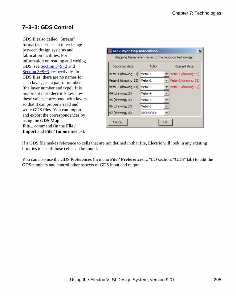
7−3−3: GDS Control
GDS II (also called "Stream"format) is used as an interchangebetween design systems andfabrication facilities. Forinformation on reading and writingGDS, see Section 3−9−2 andSection 3−9−3, respectively. InGDS files, there are no names foreach layer, just a pair of numbers(the layer number and type). It isimportant that Electric know howthese values correspond with layersso that it can properly read andwrite GDS files. You can importand export the correspondences byusing the GDS MapFile... command (in the File /Import and File / Import menus).
If a GDS file makes reference to cells that are not defined in that file, Electric will look in any existinglibraries to see if those cells can be found.
You can also use the GDS Preferences (in menu File / Preferences..., "I/O section, "GDS" tab) to edit theGDS numbers and control other aspects of GDS input and output.
Chapter 7: Technologies
Using the Electric VLSI Design System, version 9.07 205

Project Preferences
The left side of the dialog shows the Project Preferences which control the mapping of GDS layer numbers toElectric layers. The list on the left shows all of the Electric layers in the current technology. By clicking on alayer name, its GDS numbers are shown in the top−right and can be edited. GDS numbers come in a fewdifferent variations:
Normal for regular geometry.• Pin for exports.• Text for export names and special GDS text. You can use the Add GDS Text command (in menuEdit / Text
•
High V for high voltage layers. You can use the Add HV GDS Text command (in menu Edit / Text• To ignore a layer, clear the layer field (it is not sufficient to set it to zero...it must be blank).
This dialog element applies to the import of GDS:
"Scale by". This scales the GDS by the given factor when read from disk.•
Chapter 7: Technologies
206 Using the Electric VLSI Design System, version 9.07

These dialog elements apply to the export of GDS:
"Output merges Boxes". This controls the merging of adjoining geometry. It is an issue because ofthe duplication and overlap that occurs wherever arcs and nodes meet. The default action is to writeeach node and arc individually. This makes the file larger because of redundant box information,however it is faster to generate and uses simpler constructs. If you check this item, all connectingregions on the same layer are merged into one complex polygon. This requires more processing,produces a smaller file, and generates more complex constructs.
•
"Output writes export Pins". This controls whether pins are written to the GDS file for each export. Ifchecked, and there is a valid pin layer, then it is written.
•
"Output all upper case". This controls whether the GDS file uses all upper case. The default is to mixupper and lower case, but some systems insist on upper−case GDS.
•
"Output converts brackets in exports". This controls whether the square brackets used in arrayspecifications should be converted (to underscores). Some GDS readers cannot handle the squarebracket characters.
•
"Output collapses VDD/GND pin names". Requests that all names with the form "vdd_NNN" or"gnd_NNN" (where "NNN" is digits) be merged into a single power or ground signal called "vdd" or"gnd".
•
"Output writes export characteristics". Requests all GDS "pins" (Electric exports) containcharacteristics (input, output, etc.) This may be incompatible with some versions of GDS so it can bedisabled.
•
"Max chars in cell name". This limits the number of characters in a cell name. Names longer thanthis are truncated, and adjusted to ensure uniqueness.
•
"Precision" and "Units/meter" define the scaling information written to a GDS file. The Precision isthe number of units available and the Units/meter defines the size of a unit. The default Units/meteris a billion, meaning that the unit size is 1 nanometer. Note that some small feature−size technologiesmay require a larger Units/meter field. If GDS Export encounters precision errors, you will be askedto increase this value.
•
At the bottom is a setting for both export and import:
"Default text layer". This is the layer number to use for text. When exports are being written, andthere is a text layer number associated with the appropriate Electric layer, then that layer number isused instead of this default number.
•
User Preferences
These dialog elements are available on the right side (the GDS User Preferences) for import control:
"Merge boxes (slow)". This requests GDS input to combine overlapping boxes into complexpolygons. It takes more time, but produces a more compact database.
•
"Expand cells". This controls whether cell instances are expanded or not in the Electric circuit. Bydefault, cell instances are not expanded (they appear as a simple box). If you check this item, cellsare expanded so that their contents are displayed. Expansion of cells can always be changed afterreading GDS by using the subcommands of the Expand Cell Instances and Unexpand Cell
•
Chapter 7: Technologies
Using the Electric VLSI Design System, version 9.07 207

Instances commands of the Cells menu."Simplify contact vias". This requests GDS input to find combinations of metal and via cuts andreplace them with Electric contacts. It takes time, and may simplify some GDS.
•
"Instantiate arrays". This controls whether or not arrays in the GDS file are instantiated. By default,arrays are instantiated fully, but this can consume excessive amounts of memory if there are largearrays. If you uncheck this item, only the upper−left and lower−right instance are actually placed.
•
"Array simplification". This controls the simplification of special "array reference" objects in GDS.When an array of cell instances is found, and each cell instance contains a single piece of geometry,Electric can simplify the array specification so that a single pure−layer node is created instead of anarray of instances. This pure−layer node has outline information that covers each of the arrayedobjects (see Section 6−10−1 for more on outlines). This preference can be set to "None" (nosimplification of array references is used), "Merge individual arrays" in which the abovesimplification is performed, and "Merge all arrays" in which multiple array references are combinedso that a single pure−layer node is place for each layer in the cell, regardless of the number of arrayreferences that are used. This last choice can produce highly−complex pure−layer nodes, but isfastest and uses the least amount of memory.
•
"Unknown layers". This controls how unknown layers in the GDS file are treated. The default is"Convert to DRC Exclusion layer" which creates an orange DRC−Node wherever an unknown layersappears. Each DRC−Node is tagged with the unknown layer number. If you set this to "Ignore", theunknown layers are simply ignored. A final choice is "Convert to random layer" which picks adifferent layer in the technology for each unknown GDS layer number. This allows the distinctionbetween layers to be seen, even if the correct layer associations are not known.
•
"Cadence compatibility". This forces a GDS import to do things that assume the GDS has come froma Cadence system. Export locations are expanded to cover the geometry on which they reside,because Cadence allows connections to be elsewhere on the layer.. Also, Cadence style busdelimeters (<>) are converted to Electric style ([]).
•
"Dump readable data while reading" is a way to debug GDS files. When this is checked, the GDSdata is written to a text file during import, allowing you to see what is in the file.
•
These dialog elements are available on the right side (the GDS User Preferences) for export control:
"Export all cells in Library". Normally, only those cells that are part of the current hierarchy arewritten to the GDS. The current hierarchy is the current cell and all of its sub−cells. When this ischecked, every cell in the library is written. This is useful when writing out standard cell libraries.
•
"Flat design". This fully−instantiates the circuit (flattens it) before writing. Output files may be muchlarger because there is no hierarchy.
•
"Use NCC annotations for exports". The network consistency checker (NCC) allows special circuitannotations to join two networks. For example, two separate power networks may be joined higher inthe circuit hierarchy, and the NCC needs to know this at the current level of design. This checkboxrequests that the NCC annotations be used when exporting GDS. It enables external circuit analysisprograms (such as Assura) to properly understand the circuit connectivity. Specifically, when this ischecked, all of a layout cell's exports which are linked by the NCCexportsConnectedByParent annotation will be given the same GDS pin text (see Section 9−7−4 formore on NCC annotations).
•
Chapter 7: Technologies
208 Using the Electric VLSI Design System, version 9.07

These dialog elements are available on the right side (the GDS User Preferences) for export and importcontrol:
"Use visibility as filter" uses the current layer visibility as a filter for what gets imported or exported.For more on layer visibility, see Section 4−5−3.
•
"Include text". Text annotations in the GDS file can often clutter the display, so they are ignoredduring input. If you check this item, annotation text will be read and displayed.
•
7−3−4: EDIF Control
EDIF (Electronic Design Interchange Format) is used to exchange design information between differentCAD systems. Although EDIF is currently at version "4 0 0", Electric reads and writes version "2 0 0".
For moreinformation onreading andwriting EDIF,see Section3−9−2 andSection 3−9−3,respectively.EDIF optionsare controlledwith the EDIFPreferences (inmenu File /Preferences...,"I/O" section,"EDIF" tab).
These controls are supported by the dialog:
Use Schematic View when writing controls whether EDIF output writes schematic or netlist views(the default is netlist).
•
Scale by lets you set a scale factor for EDIF input.• Stitch cells when reading invokes the Auto Stitching router after EDIF import to make explicitconnections (see Section 9−6−2 for more)
•
Cadence compatibility affects both EDIF input and output. When checked, output ofmultidimensional and symbolic busses is converted to simpler, all−numeric busses, and input of
•
Chapter 7: Technologies
Using the Electric VLSI Design System, version 9.07 209

properties starting with "def" are added to cells as parameters.Show arc names and Show node names controls whether EDIF input makes arc and node namesvisible.
•
Accepted Parameters lets you list those EDIF parameters that will be read (all others are ignored).•
The bottom section of the panel lets you specify a configuration file that will control EDIF I/O. This file hasconversions between coordinates and names inside of Electric and the EDIF file. The file has these lines oftext that control different aspects of conversion:
Primitives A line starting with "P" controls how primitives are converted to EDIF. The line has thisformat: P ElTech ElPrim ElFunc ElRot ElPortOff EdTech EdPrim EdFunc EdPortOff
Where: ElTech is the Electric technology name (e.g. "schematic").♦ ElPrim is the Electric primitive name (e.g. "Transistor").♦ ElFunc is the Electric function (e.g. "CONPOWER").♦ ElRot is the Electric rotation (e.g. "90").♦ ElPortOff is the Electric port offsets, enclosed in braces (e.g. "{ g(−1,0) }"). The offsetsare the values required to move the port to the origin, so if a port is at (2, −5), the offsetshould be (−2, 5). Each port on the primitive must be listed, and an offset given. To ignore aport, use "NA" instead of "port(x,y)". You can also specify an ignored port as "NA(x,y)" ifyou want to affect how an attached wire's endpoint is modified. "NA" by itself is the same as"NA(0,0)". If the port's name is "NA", use "\NA(x,y)" to specify the name as NA, and not beignored.
♦
EdTech is the EDIF technology name (e.g. "tsmc18").♦ EdPrim is the EDIF primitive name (e.g. "pmos2v").♦ EdFunc is the EDIF function (e.g. "symbol").♦ EdPortOff is the EDIF port offsets, enclosed in braces (e.g. "{ G(0,0) }"). Each port onthe primitive must be listed, and an offset given. The offsets are the values required to movethe port to the origin, so if a port is at (2, −5), the offset should be (−2, 5).
♦
For example: P schematic Ground CONGROUND 0 { gnd(0,2) } basic gnd symbol { gnd!(0,0) }
•
Cells A line starting with "C" controls how cells are converted to EDIF. The line has this format: C ElLib ElCell ElView ElRot ElPortOff EdTech EdPrim EdFunc EdPortOff
Where: ElLib is the Electric library name (e.g. "MyCells").♦ ElCell is the cell name in that library (e.g. "Inverter").♦ ElView is the view name of the cell (e.g. "ic" for Icon).♦
All other fields are the same as in the "Primitive" line.
•
Exports A line starting with "E" controls how exports are converted to EDIF. The line has thisformat: E ElTech ElPrim ElFunc ElRot ElPortOff EdTech EdPrim EdFunc EdPortOff
Where: ElTech is the Electric technology name (e.g. "schematic").♦ ElPrim is the Electric primitive name (e.g. "Transistor").♦
•
Chapter 7: Technologies
210 Using the Electric VLSI Design System, version 9.07

ElFunc is the Electric function (e.g. "CONNECT").♦ ElRot is the Electric rotation (e.g. "90").♦ ElPortOff is the Electric port offsets, enclosed in braces (e.g. "{ g(−1,0) }"). The offsetsare the values required to move the export to the origin, so if an export is at (2, −5), the offsetshould be (−2, 5). Each port on the primitive must be listed, and an offset given.
♦
EdTech is the EDIF technology name (e.g. "tsmc18").♦ EdPrim is the EDIF primitive name (e.g. "pmos2v").♦ EdFunc is the EDIF function (e.g. "symbol").♦ EdPortOff is the EDIF port offsets, enclosed in braces (e.g. "{ G(0,0) }"). The offsets arethe values required to move the export to the origin, so if an export is at (2, −5), the offsetshould be (−2, 5). Each port on the primitive must be listed, and an offset given.
♦
For example: E schematic Off−Page CONNECT 0 input { a(−2,0), y(2,0) } basic ipin symbol {
NA, NA }
Variables A line starting with "V" controls how variables are converted to EDIF. The line has thisformat: V ElVarName EdVarName Scale [Append]
Where: ElVarName is the Electric variable name (e.g. "ATTR_M").♦ EdVarName is the EDIF primitive name (e.g. "m").♦ Scale is a scale from Electric to EDIF (e.g. "1").♦ Append is an optional string to append to EDIF (e.g. "u").♦
For example: V ATTR_length l 0.9 u
•
FigureGroups A line starting with "F" controls how figure groups are converted to EDIF. The linehas this format: F ElName EdName
Where: ElName is the Electric technology name (e.g. "ARTWORK").♦ EdName is the EDIF figure group name (e.g. "DEVICE").♦
For example: F ARTWORK DEVICE
•
Globals A line starting with "G" controls how global names are converted to EDIF. The line has thisformat: G ElName EdName
Where: ElName is the Electric global name (e.g. "GND").♦ EdName is the EDIF global name (e.g. "gnd!").♦
For example: G GND gnd!
•
Chapter 7: Technologies
Using the Electric VLSI Design System, version 9.07 211

7−3−5: LEF/DEF Control
LEF (Library Exchange Format) and DEF (Design Exchange Format) are recent interchange formats forCAD systems. For more information on reading and writing LEF and DEF, see Section 3−9−2 and Section3−9−3, respectively.
LEF options are controlledwith the LEF Preferences(in menu File /Preferences..., "I/O"section, "LEF" tab). Youcan choose whether or notto ignore ungenerated pins.Ungenerated pins are thosethat have no locationinformation, and are notfully part of the design. Ifthey are not ignored (thebox is unchecked) they areplaced at the origin. Youcan choose what to do withunrecognized layers (eitherignore them or use theDRC−exclusion layer). Youcan also ask Electric toignore any technologyinformation when readingthe LEF file.
Chapter 7: Technologies
212 Using the Electric VLSI Design System, version 9.07

DEF options arecontrolled with theDEF Preferences (inmenu File /Preferences..., "I/O"section, "DEF" tab).This dialog controlswhether DEF readsphysical and/or logicalinformation. If a typeof interconnect is notchecked, the DEFinput reader ignoresthose arcs.
DEF interconnect is specified in the NETS and SPECIALNETS sections. Typically, the SPECIALNETS arepre−routed geometry (physical) and the NETS are routed geometry (physical) or unrouted information(logical). Check "Ignore physical interconnect in NETS section" to skip any routed arcs (physical) found inthe NETS section. Check "Ignore logical interconnect in SPECIALNETS section" to skip any unrouted arcs(logical) found in the SPECIALNETS section.
Physical NETS are read as arcs on different layers that connect the circuitry. This can take a lot of time toplace. If it takes too long, and if the connectivity information is not needed, check "Use pure−layer nodesinstead of arcs" to use pure−layer nodes instead of arcs.
When unknown cells are referenced by the DEF file, an error is issued. If "Make dummy cells for unknowncells" is checked, the system resolves the problem by generating the appropriate cell.
The "Ignore ungenerated pins (with no location)" option determines how to handle ungenerated pins.Ungenerated pins are those that have no location information, and are not fully part of the design. If they arenot ignored (the box is unchecked) they are placed at the origin.
The "Ignore vias block" option causes vias to be dropped from import.
The "Place and connect all pin geometry" option connects like−named exports (called "pins" by Cadence)with unrouted arcs. Because Cadence systems give electrically−connected pins the same name, thoselike−named pins should all be connected. This option connects them in such a way that routers can wire themtogether.
Chapter 7: Technologies
Using the Electric VLSI Design System, version 9.07 213

Finally, you can control what happens to unrecognized layers (either ignore them or convert them to theDRC−exclusion layer).
7−3−6: CDL Control
CDL (Circuit DescriptionLanguage) is almost identicalto Spice format, and is used asa netlist interchange method.CDL options are controlledwith the CDL Preferences (inmenu File / Preferences...,"I/O" section, "CDL" tab).Additional CDL options thatare common to Spice optionscan be found in the Spice/CDLPreferences (in menu File /Preferences..., "Tools"section, "Spice/CDL" tab).
This dialog controls the libraryname and path informationthat is written when generatinga netlist. You can specify anInclude file which will beinserted at the top of thenetlist. Also, you can chooseto convert square−bracketcharacters (if your CDL cannothandle indexed signal names).
Chapter 7: Technologies
214 Using the Electric VLSI Design System, version 9.07

7−3−7: DXF Control
DXF (Drawing eXchange Format) is a solid modeling format used by AutoCAD systems. For moreinformation on reading and writing DXF, see Section 3−9−2 and Section 3−9−3, respectively.
DXF I/O is controlled with the DXF Preferences (in menu File / Preferences..., "I/O section, "DXF" tab).
The Project Preferences part of the dialog controls the list of acceptable DXF layers.
These layerscan be typedinto the editfield, separatedby commas. Ifa layer name inthe DXF file isnot found inthe list ofacceptablelayers, it willbe ignored.
To control scaling, you can change the meaning of units in the DXF file. The default unit is "Millimeters",which means that a value of 5 in the DXF file becomes 5 millimeters in Electric.
The User Preferences part of the dialog controls DXF input. By default, Electric flattens DXF input,removing levels of hierarchy and creating a single cell with the DXF artwork. By unchecking the "Inputflattens hierarchy", Electric will preserve the structure of the DXF file.
If you uncheck "Input reads all layers", then unknown layers are not read into Electric.
Chapter 7: Technologies
Using the Electric VLSI Design System, version 9.07 215

7−3−8: SUE Control
SUE (Schematic User Environment) is the database format of the SUE schematic editor, from MicroMagic (www.micromagic.com). For more information on reading SUE, see Section 3−9−2.
SUE options are controlledwith the SUE Preferences (inmenu File / Preferences...,"I/O" section, "SUE" tab). Thisdialog has two controls:
"Make 4−porttransistors" requeststhat transistors be4−port (with asubstrate connection).The default is 3−port.
•
"Convert Sueexpressions toElectric" requests thatSUE expressions beanalyzed for parameterreferences andconverted to Electricparameter form (withan "@" in front of theparameter name).
•
Chapter 7: Technologies
216 Using the Electric VLSI Design System, version 9.07

7−3−9: Gerber Control
Gerber is a printed−circuit board layout format, originally from Gerber Scientific. For more information onreading Gerber, see Section 3−9−2.
Gerber options are controlledwith the Gerber Preferences(in menu File / Preferences...,"I/O" section, "Gerber" tab).This dialog has two controls:
"Fill polygons"requests that polygonsbe filled−in instead ofoutlined.
•
"Read all .GBR filesin the directory"requests that theimport function scanfor other files endingin ".GBR" and read allof them.
•
Chapter 7: Technologies
Using the Electric VLSI Design System, version 9.07 217

7−3−10: SVG Control
SVG (Scalable Vector Graphics) is a format for web browsers. For more information on writing SVG, seeSection 3−9−3.
SVG options are controlled with theSVG Preferences (in menu File /Preferences..., "I/O" section, "SVG"tab). This dialog has two controls:
"Scale Factor" specifies howElectric units are scaled intoSVG units. The default (1)makes a SVG file that usesexact Electric coordinates.
•
"Margin" is the number ofSVG units that are added tothe top and left.
•
Chapter 7: Technologies
218 Using the Electric VLSI Design System, version 9.07

7−4: The MOS Technologies
7−4−1: Introduction to MOS Technologies
There are both nMOS and CMOS technologies available in Electric, with many different design rules. Usethe popup at the top of the component menu to select a different MOS technology.
There is one nMOS technology: "nmos" (the specifications used in the Mead and Conway textbook).
There are a few CMOS technologies available. The most basic is "cmos", which uses an idealized set ofdesign−rules from a paper by Griswold. The most popular CMOS technology is "mocmos" (MOSIS designrules) which has two layers of polysilicon and up to 6 layers of metal with standard, submicron, or deep rules(this is described more fully in the next Section). There is even "rcmos", which uses round geometry!
Each MOS technology has two transistors(enhancement and depletion in nMOStechnologies, n and p in CMOS). These nodescan have serpentine paths by highlightingthem and using "Outline Edit" mode (seeSection 6−10−1).
The contact nodes in the MOStechnologies automaticallyincrease the number of cut layerswhen the contact grows in size.For very large contacts, however,the display of these cuts can wastetime. Therefore, when very largecontacts are displayed at smallscale, the interior cuts may not bedrawn (as shown on the right).
Be assured, however, that the cuts are actually there, and will appear in all appropriate output.
Chapter 7: Technologies
Using the Electric VLSI Design System, version 9.07 219

Contact nodes also have theability to place the cutsaccording to different rules.The default (shown on theleft) is to pack them asclosely as possible in thecenter of the contact.
Using the Object Properties... command (in menu Edit / Properties) you can change the "Cut Placement"to "At node edges" (the middle example) or "In node corner" (the rightmost example).
Although individual MOS nodes and arcs have the proper amount of implant around them, a collection ofsuch objects may result in an irregular implant boundary. To clean this up, you can place pure−layer nodes ofimplant that neatly cover the implant area. Also, you can do this automatically with the Coverage ImplantsGenerator command (in menu Tools / Generation, see Section 9−8−2).
7−4−2: The MOSIS CMOS Technology
The MOSIS CMOS technology describesa scalable CMOS process that is fabricatedby the MOSIS project of the University ofSouthern California. To obtain thistechnology, use the popup menu at the topof the component tab (in the side bar) andselect "mocmos".
This technology can have from 2 to 6layers of metal (4 are shown here, 6 is thedefault). It has 1 polysilicon layer but canbe changed to use 2. The technology canbe set to use either standard rules(SCMOS), submicron rules, or deep rules.You can choose whether to allow stackedvias and whether or not to use alternatecontact rules. Finally, you can set thetechnology into "Analog" mode, whichprovides an NPN transistor, a PolysiliconCapacitor, and many resistors. This isdone with the Technology Preferences (inmenu File / Preferences..., "Technology"tab).
The default orientation of transistors (both in the menu, and when first placed) can be rotated by checking"Rotate transistors in menu" in the Technology Preferences.
Chapter 7: Technologies
220 Using the Electric VLSI Design System, version 9.07

Users of Electric version 6.02 or earlier will have a different MOSIS CMOS technology called"mocmossub". This technology attempted to match the submicron rule set, but did not do so as accurately asthe current "mocmos" technology. If you have designs in that technology, they will be automaticallyconverted to the new "mocmos" when read in.
Scalable Transistors
The MOSIS CMOS technology has two transistor nodes that can take a text attribute to control their width.These transistors also have contacts built into them. Without the text attribute, the maximum width isdisplayed. However, by adding a "width" attribute, they shrink to that size. Note that the ports never changelocation, thus allowing them to scale without triggering constraints. The scaling feature of these transistors isnot very useful because it is not possible to parameterize layout cells.
Chapter 7: Technologies
Using the Electric VLSI Design System, version 9.07 221

The scalable transistor onthe left is 3 wide, and theother two are 10 wide.However, the scalabletransistor on the right hasthe "width" set to 8, so it hasshrunk.
If you get ObjectProperties... on a scalabletransistor, there are extracontrols that let you chooseto have fewer contacts (1 oreven none), and you cantighten the contact spacing.
Chapter 7: Technologies
222 Using the Electric VLSI Design System, version 9.07

7−5: Schematics
7−5−1: Introduction to Schematics
The Schematic technologyallows you to design usingdigital and analog schematiccomponents. To obtain thistechnology, use the popup menuat the top of the componentmenu and select "schematics".
There are two arcs in theSchematic technology: the wire(blue) and the bus (green). Thesearcs can be drawn at 45 degreeangles. One typically namesbusses with array names (forexample "insig[0:7]"), and thennames wires with scalar names(for example "insig[1]"). SeeSection 6−9−3 for more on busnaming.
To make a physical connectionfrom a wire to a bus, the bus pincan connect to either, so it acts asa tap. In addition, the Wire Connode connects wires to busses, orconnects busses of differentwidth, replicating the narrowerside to make it as wide as thewider side. Use the RipBus command (in menu Edit /Arc) to automatically add taps toa bus.
There are four transistor entries in the menu. The two on the right are the n and p transistors. The two imageson the left are actually popup menus that let you select any style of transistor. The difference between the twoon the left is that the top one is for 3−port transistors, and the bottom one is for 4−port transistors. Theschematics technology understands these transistor types:
Chapter 7: Technologies
Using the Electric VLSI Design System, version 9.07 223

nMOS / pMOS n− and p−channel MOS transistors.• nMOS−D / pMOS−D depletion MOS transistors.• nMOS−NT / pMOS−NT native MOS transistors.• nMOS−FG / pMOS−FG floating−gate MOS transistors.• nMOS−CN / pMOS−CN carbon nanotube MOS transistors.• nMOS−VTL / pMOS−VTL low−threshold MOS transistors.• nMOS−VTH / pMOS−VTH high−threshold MOS transistors.• nMOS−HV1 / pMOS−HV1 high−voltage (1: lowest voltage) MOS transistors.• nMOS−HV2 / pMOS−HV2 high−voltage (2: medium voltage) MOS transistors.• nMOS−HV3 / pMOS−HV3 high−voltage (3: highest voltage) MOS transistors.• nMOS−NT−HV1 / pMOS−NT−HV1 native, high−voltage (1: lowest voltage) MOS transistors.• nMOS−NT−HV2 / pMOS−NT−HV2 native, high−voltage (2: medium voltage) MOS transistors.• nMOS−NT−HV3 / pMOS−NT−HV3 native, high−voltage (3: highest voltage) MOS transistors.• PNP / PNP bipolar transistors.• DMES / EMES MESFET transistors.• pJFET / nJFET JFET transistors.•
Other primitives that can appear in different forms:
Capacitors can be normal or electrolytic.• Diodes can be normal or zener.• Resistors can be normal, n−Poly, p−Poly, n−Well, or p−Well.• Off−page connectors appear differently depending on their export's characteristics (input, output, etc.)•
The "Spice" entry presents a popup menu of Spice parts. More information about the use of these parts can befound in the Section 9−4−3.
The "Cell" entry presents a popup menu of all cell instances.
The "Global" entry provides two nodes: a "Global Signal" node defines a signal name that spans levels ofhierarchy, and a "Global Partition" node allows globals to be treated locally. See Section 6−9−5 for more onglobal networks.
Some commands that analyze a schematic circuit need to know which layout technology will be used tofabricate the design. For example, when generating a Spice deck from a schematic, it is necessary to knowthe sizes and parasitics that are associated with the actual circuit. To set the layout technology to use forschematic circuits, use the Technology Preferences (in menu File / Preferences..., "Technology" section,"Technology" tab), and set the "Use scale values from this technology" popup.
Chapter 7: Technologies
224 Using the Electric VLSI Design System, version 9.07

Digital Schematics
Digital schematics are built with the And, Or, Xor, Buffer, Multiplexor, and Flip−Flop nodes that appear inthe component menu. By attaching arcs to these components and negating them (with the Toggle PortNegation command, in menu Edit / Technology Specific), these turn into NAND, NOR, Inverter, and manyother specialized components (see Section 5−4−2).
The And, Or, Xor, and Multiplexor nodes can accept any number of input connections on the left, so theyrequire some care in wiring (see Section 1−11−5). The left side has one large input port that allows anarbitrary number of connections. Initially, wires may attach at only three input locations, spaced evenly alongthe left side. However, when all three locations are connected, the node automatically expands, addingadditional space along the side for new arcs.
To properly wire inputs to an And, Or, Xor, or Multiplexor node, cursor placement is very important, for itdetermines which of the locations to use on the left side. If an arc gets connected in the wrong location, tryconnecting more arcs until one appears in the right place, and then delete the unwanted ones.
The Switch node can also take an arbitrary number of poles on its left side. Simply stretch it along the line ofthe poles and their number will grow.
Analog Schematics
The analog nodes (Resistor, Inductor, Capacitor, and Diode) have values on them which can be selected andedited. Double−clicking on them brings up a special dialog for editing their value.
The Resistor can be treated as a connecting or nonconnecting node. By default, it does not connect thenetworks on its two ends, and this is the correct way to treat it when doing low−level simulation such asSpice. However, for higher−level simulations (such as Verilog) the resistor should be ignored and treated asif it connects its two networks. To make this happen, use the Networks Preferences (in menu File /Preferences..., "Netlists" tab), and check "Ignore Resistors when building netlists". Note that if resistors arebeing ignored, Spice deck generation will temporarily include them while the netlist is being created.
Chapter 7: Technologies
Using the Electric VLSI Design System, version 9.07 225

7−5−2: Multipage Schematics and Frames
Multipage schematics are implemented in Electric by having each page map to a different area of a vastschematic cell. To create one of these multipage cells, use the Make Cell Multi−Page command (in menuCell / Multi−Page Cells). You will then be editing page 1 of the multi−page schematic.
You can add pages to the current multipage schematic with the Create New Page command (in menu Cell /Multi−Page Cells). You can delete the current page with Delete This Page. To advance to the next page, useEdit Next Page.
Older versions of Electric implemented multipage schematics with different view types ("p1", "p2", ...). Ifthese views appear instead of proper pages, use the Convert old−style Multi−Page Schematics command.
As a graphical aid to schematic design, frames can be displayed in a cell by using the CellProperties... command (in menu Cell). Multi−page schematics require a cell frame on every page, but theirpresence is optional in other cells.
The frame size can be "Half−A", "A", "B", "C", "D", and "E". The frame can be horizontal (landscape) orvertical (portrait). You can choose to display a title box in the lower−right corner. The designer name canalso be set for each cell.
Chapter 7: Technologies
226 Using the Electric VLSI Design System, version 9.07

Besides the designer name, cell frames have a company name and a project name. These values are not setfor each cell, but instead are preferences that are set for each user. Individual libraries can override thesedefaults as well.
The FramePreferences (in menuFile / Preferences...,"Display" section,"Frame" tab) lets youset all of thesedefaults. Note thatthe designer name istaken first from thecell, then from thelibrary if the cell doesnot set a value, andfinally from thegeneral default if thelibrary and cell donot set a value.
Chapter 7: Technologies
Using the Electric VLSI Design System, version 9.07 227

7−6: Special Technologies
7−6−1: The Artwork Technology
The Artwork technology is an unusual technology that provides general−purpose sketching facilities. Toobtain this technology, use the popup menu at the top of the component menu and select "artwork".
This technology has nodes formany typical graphic objects suchas rectangles, triangles, circles,and arrowheads. Polygonal andSpline nodes allow arbitraryshapes to be defined. Of course,nodes from all other technologiescan be used as special electronicsymbols when artwork isgenerated. Conversely, theseartwork nodes can be used toembellish designs done in all othertechnologies.
Circles can be outlines (normal orthick) or filled. The default shapeis round, but elongation of thenode produces an ellipse. Inaddition, by using the ObjectProperties... command (in menuEdit / Properties), the outlinecircles can be reduced to a portionof the circle (from 1 to 360degrees).
The "Export" entry creates an export for use in icons. After clicking on the entry, you have the choice ofselecting "Wire", "Bus", or "Universal" exports (see Section 3−11−4 for more on icon generation).
There are four different polygon styles: opened, closed, filled, and spline. The opened polygon can be drawnwith solid lines, dotted lines, dashed lines, or thicker lines. These nodes require that you use the "OutlineEdit" mode (see Section 6−10−1).
Chapter 7: Technologies
228 Using the Electric VLSI Design System, version 9.07

The illustration below shows how outline information, applied to Artwork nodes, results in different shapes.In each of the shapes, the outline has the same 5 points, as illustrated in the upper−left. The nodes interpretthis outline information to produce their shape. Note that the spline curve does not run through the outlinepoints, only near them.
The final feature of the Artwork technology is its ability to set the appearance of any of its nodes or arcs. Usethe Artwork Color and Pattern... command (in menu Edit / Technology Specific) to set the color andpattern of any Artwork node or arc. You can also invoke this dialog by clicking on the "Color and Pattern..."button in the node or arc "Properties" dialogs. You can set the color, pattern, and outline texture of anyArtwork node and arc. Predefined patterns are available below the pattern−editing area. If transparent colorsare selected, they are taken from the current color map, which in turn is taken from the most recently selectedtechnology (other than the Artwork technology). Note that artwork elements which do not have a colorassigned use the DEFAULT−ARTWORK color (see Section 4−6−2).
Chapter 7: Technologies
Using the Electric VLSI Design System, version 9.07 229

7−6−2: The FPGA Technology
The FPGA technology is a "soft" technology that creates primitives according to an FPGA Architecture file.Special commands in the Edit / Technology Specific / FPGA menu let you create the FPGA primitives,build FPGA structures, and program them.
The FPGA Architecture file contains all of the information needed to define a specific FPGA chip. It hasthree sections: the Primitive Definition section, the Block Definition section, and the Architecture section.The Primitive Definition section describes the basic blocks for a family of FPGA chips (these are primitivesin the FPGA technology). The Block Definition section builds upon the primitives to create higher−levelblocks. Finally, the Architecture section defines the top−level block that is the FPGA.
An FPGA Architecture file must have the Primitive Definition section, but it need not have the BlockDefinition or Architecture Sections. This is because the placement of the primitives can be saved in anElectric library, rather than the architecture file. Thus, after reading the Primitive Definition section (whichcreates the primitives), and reading the Block Definition and Architecture Sections (which places theprimitives to create a chip library) the library can be saved to disk. Subsequent design activity can proceed byreading only the Primitive Definition section and then reading the library with the chip definition. Thisavoids large FPGA Architecture files (the Primitive Definition section will be smaller than the BlockDefinition and Architecture sections).
Chapter 7: Technologies
230 Using the Electric VLSI Design System, version 9.07

Primitive Definition Section
The Primitive Definition section defines the lowest−level blocks, which become primitive nodes in the FPGAtechnology. A primitive definition looks like this:
(primdef (attributes (name PRIMNAME) (size X Y) ) (ports (port (name PORTNAME) (position X Y) (direction input | output | bidir) ) ) (components (pip (name PIPNAME) (position X Y) (connectivity NET1 NET2) ) ) (nets (net (name INTNAME) (segment FROMPART TOPART) ) ))
The attributes section defines general information about the block. The ports section defines externalconnections. The components section defines logic in the block (currently only PIPs). The nets sectiondefines internal networks. There can be multiple segment entries in a net, each defining a straight wire thatruns from the FROMPART to the TOPART. These parts can be either port PORTNAME or coord X Y,depending on whether the net ends at a port or at an arbitrary position inside of the primitive.
Chapter 7: Technologies
Using the Electric VLSI Design System, version 9.07 231
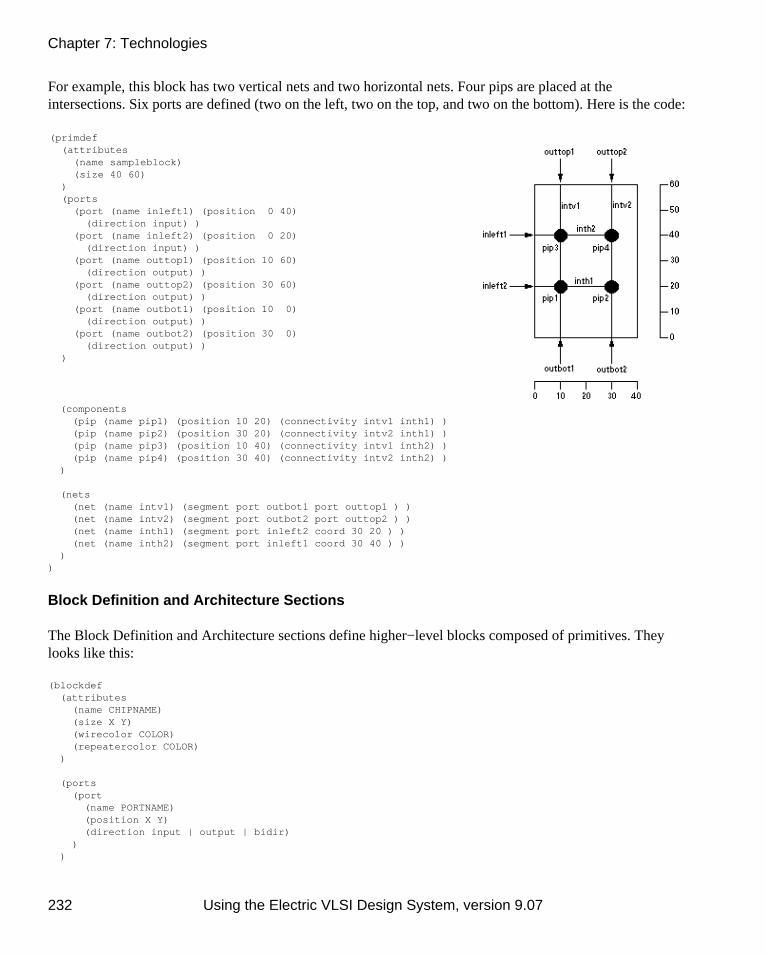
For example, this block has two vertical nets and two horizontal nets. Four pips are placed at theintersections. Six ports are defined (two on the left, two on the top, and two on the bottom). Here is the code:
(primdef (attributes (name sampleblock) (size 40 60) ) (ports (port (name inleft1) (position 0 40) (direction input) ) (port (name inleft2) (position 0 20) (direction input) ) (port (name outtop1) (position 10 60) (direction output) ) (port (name outtop2) (position 30 60) (direction output) ) (port (name outbot1) (position 10 0) (direction output) ) (port (name outbot2) (position 30 0) (direction output) ) )
(components (pip (name pip1) (position 10 20) (connectivity intv1 inth1) ) (pip (name pip2) (position 30 20) (connectivity intv2 inth1) ) (pip (name pip3) (position 10 40) (connectivity intv1 inth2) ) (pip (name pip4) (position 30 40) (connectivity intv2 inth2) ) )
(nets (net (name intv1) (segment port outbot1 port outtop1 ) ) (net (name intv2) (segment port outbot2 port outtop2 ) ) (net (name inth1) (segment port inleft2 coord 30 20 ) ) (net (name inth2) (segment port inleft1 coord 30 40 ) ) ))
Block Definition and Architecture Sections
The Block Definition and Architecture sections define higher−level blocks composed of primitives. Theylooks like this:
(blockdef (attributes (name CHIPNAME) (size X Y) (wirecolor COLOR) (repeatercolor COLOR) )
(ports (port (name PORTNAME) (position X Y) (direction input | output | bidir) ) )
Chapter 7: Technologies
232 Using the Electric VLSI Design System, version 9.07

(components (instance (attributes ATTPAIRS) (type BLOCKTYPE) (name BLOCKNAME) (position X Y) (rotation ROT) ) (repeater (name BLOCKNAME) (porta X Y) (portb X Y) (direction vertical | horizontal) ) )
(nets (net (name INTNAME) (segment FROMPART TOPART) ) ))
The only difference between the Architecture section and the Block Definition section is that the Architecturesection has the keyword architecture instead of blockdef. There can be only onearchitecture section, but there can be many blockdefs, defining a complete hierarchy.
The attributes section defines general information about the block.
The ports section defines external connections.
The components section defines logic in the block (currently instances of other blocks or repeaters). Therotation of an instance is the number of degrees counterclockwise, rotated about the center. Theattributes section of the instance assigns name/value pairs (this can be used to program the FPGA).
The nets section defines internal networks. There can be multiple segment entries in a net, each defininga straight wire that runs from the FROMPART to the TOPART. These parts can be either componentINSTNAME PORTNAME, port PORTNAME, or coord X Y, depending on whether the net ends at acomponent, port or at an arbitrary position inside of the block.
Chapter 7: Technologies
Using the Electric VLSI Design System, version 9.07 233

Here is an example of block definition code and its layout.
(blockdef (attributes (name testblock) (size 80 150) ) (components (instance (type sampleblock) (name block0) (position 30 80) ) (instance (type sampleblock) (name block1) (position 30 10) ) (repeater (name r0) (porta 10 120) (portb 20 120) (direction horizontal) ) (repeater (name r1) (porta 10 100) (portb 20 100) (direction horizontal) ) (repeater (name r2) (porta 10 50) (portb 20 50) (direction horizontal) ) (repeater (name r3) (porta 10 30) (portb 20 30) (direction horizontal) ) )
(ports (port (name top0) (position 40 150) (direction bidir) ) (port (name top1) (position 60 150) (direction bidir) ) (port (name left0) (position 0 120) (direction input) ) (port (name left1) (position 0 100) (direction input) ) (port (name left2) (position 0 50) (direction input) ) (port (name left3) (position 0 30) (direction input) ) (port (name bot0) (position 40 0) (direction bidir) ) (port (name bot1) (position 60 0) (direction bidir) ) )
(nets (net (name iv0) (segment port top0 component block0 outtop1) ) (net (name iv1) (segment port top1 component block0 outtop2) ) (net (name iv2) (segment component block0 outbot1 component block1 outtop1)) (net (name iv3) (segment component block0 outbot2 component block1 outtop2)) (net (name iv4) (segment component block1 outbot1 port bot0) ) (net (name iv5) (segment component block1 outbot2 port bot1) ) (net (name ih0) (segment port left0 component r0 a) ) (net (name ih1) (segment component r0 b component block0 inleft1) ) (net (name ih2) (segment port left1 component r1 a) ) (net (name ih3) (segment component r1 b component block0 inleft2) ) (net (name ih4) (segment port left2 component r2 a) ) (net (name ih5) (segment component r2 b component block1 inleft1) ) (net (name ih6) (segment port left3 component r3 a) ) (net (name ih7) (segment component r3 b component block1 inleft2) ) ))
Chapter 7: Technologies
234 Using the Electric VLSI Design System, version 9.07

Commands
To read an architecture file, use the Read Architecture And Primitives... command (in menu Edit /Technology Specific / FPGA). You will be prompted for an architecture file. To read only the primitivesfrom an architecture file, use the Read Primitives... command.
Once an FPGA is on the screen, two aspects of its display can be controlled: the wires and the text. Threecommands control the display of wires: Show All Wires displays every wire, Show No Wires hides everywire, and Show Active Wires shows only the wires that have been connected to PIPs that have beenprogrammed. Two commands control the display of text: Show Text displays text and Hide Text turns textdisplay off.
Once an FPGA has been created, you can program the PIPs by selecting a component and using the EditPips... command. This will display a list of active PIPs on the component. For example, after clicking on oneof the "SampleBlock" instances, you can type the string "pip1 pip4" to program two of the pips in thatinstance.
7−6−3: The Generic Technology
One particularly interesting technology is the Generic technology, which is a grab bag of miscellaneousfacilities. It is not necessary to actually switch into this technology, for all of its nodes and arcs are availablethrough other means.
Special Arcs
The Universal arc in the Generic technology is able to make a connection between any two components,even if they are in different technologies. This is useful when mixing technologies while still maintainingproper connectivity, for example when simulating.
The Invisible arc attaches any two components, but makes no electrical connection. It is useful forconstraining otherwise unrelated components.
The Unrouted arc makes arbitrary electrical connections, like the universal arc, but routers know to replacethem with real geometry.
None of these arcs produce any actual geometry in IC descriptions, but they make important conceptualconnections. Any existing arc in a normal technology can be converted to one of these three special arcs byusing the Change... command (in menu Edit).
Chapter 7: Technologies
Using the Electric VLSI Design System, version 9.07 235

Special Nodes
There are also special nodes in the Generictechnology. They are all available from the"Misc." entry of the component menu.
A special primitive, called Cell Center, definesthe origin of any cell. Once the node is placed,its location is at (0,0) for the cell. Sinceinstances of the current cell use the origin asthe anchor point for cursor−based references,the location of this node defines the anchor.For example, if you place this node in theupper−right corner of a cell, then creationcommands place instances such that theirupper−right corner is at the cursor. See Section3−3 for more information on cell centers.
A special primitive, called Essential Bounds,defines an alternate boundary of any cell. Atleast two of them must be placed in oppositecorners, although 4 can be place to make itlook better.
Note that the Cell Center and Essential Boundsnodes are made "hard−to−select" by default,which means that they can be selected only byusing "Special Select" mode (see Section2−1−5 for more).
The Spice Code and Spice Declaration entries create text for Spice decks (see Section 9−4−3). The VerilogCode, Verilog Declaration, Verilog Parameter, and Verilog External Code entries create text for Verilogdecks (see Section 9−4−2). These entries actually create Invisible Pin nodes with appropriate text on them.
A special primitive, called Simulation Probe is recognized by simulators and visually modified to reflectwhatever it is connected to. The simulators that reflect the state of the circuit by drawing lines along arcs alsofill−in these probe nodes. It provides a visual display of simulation activity, and works especially well withthe VCR controls in the waveform window. See Section 4−11 for more.
The DRC Exclusion node is used by the design−rule checker (see Section 9−2−3). The RoutingExclusion node is used by routers to tell them to avoid certain layers under this node (see Section 9−6−1).Currently only the Sea−of−Gates router handles this. The AFG Exclusion node is used by the auto−fillgenerator (see Section 9−8−2).
Chapter 7: Technologies
236 Using the Electric VLSI Design System, version 9.07

The Invisible Pin is used for holding text, and it does not appear in hardcopy output (this is what is createdwhen you use place Annotation Text). This pin can connect to any arc.
The Universal Pin is a node that can connect to any arc. This is useful as an intermediate component whenreplacing (first you replace the unwanted node with a Universal−Pin to allow it to fit with the existing arcs;then you replace the arcs; finally you put the desired new node in place).
The Unrouted Pin is used when joining unrouted arcs. It can also connect to anything.
Chapter 7: Technologies
Using the Electric VLSI Design System, version 9.07 237

Chapter 7: Technologies
238 Using the Electric VLSI Design System, version 9.07

Chapter 8: Creating New Technologies
8−1: Technology Editing
Although there are many technology descriptions in Electric, there are many more in the world. Toaccommodate this, there are three ways to define a technology in Electric:
The Technology Editor allows you to modify existing technologies and create new ones. Thetechnology editor is describe here and in Sections 8−2 through 8−9.
•
The Technology Creation Wizard constructs technologies from simple process parameters. Thetechnology creation wizard is described in Section 8−11.
•
The Technology XML Files define technologies and can be created or hand−edited. The file format isdescribed in Section 8−10.
•
The technology editor works by converting a technology into a library of cells. You then edit the cells, usingfamiliar Electric commands, and make changes to the technology. Finally, the technology editor translatesthe library back into a new technology.
Using the Electric VLSI Design System, version 9.07 239

Libraries which describe a technology arecalled technology libraries. They useelements from the Artwork technology todescribe their information. Specialcommands from the Edit / TechnologyEditing menu aid in the manipulation ofthese libraries.
There are four types of cells in atechnology library which describe thelayers, arcs, nodes, and support. They areseparated into these groups in the cellexplorer. The layer cells all begin with thename "layer−" and each one defines alayer in the technology. For example, thecell called "layer−Metal" defines themetal layer. The node and arc cellscorrespond to the primitives in thetechnology. Their names always beginwith "node−" and "arc−". The support cellis always called "factors". Any other cellin the library is ignored.
Chapter 8: Creating New Technologies
240 Using the Electric VLSI Design System, version 9.07

8−2: Converting between Technologies and Libraries
Converting Technologies to Libraries
The best way to create a new technology is to change an existing one. Use the Convert Technology toLibrary for Editing... command (in menu Edit / Technology Editing) and select a similar technology.Unfortunately, the Schematic and Artwork technologies are too complex to edit and cannot be converted.
Conversion of a technology to a library creates a library with the same name as the technology. Note thattechnologies with settings (such as MOSIS CMOS) will be converted with their current settings only, and theoptions will no longer be available.
Technology−Editing Mode
Once a technology−library has been created, editing of its cells is done in a special technology−editing mode.The system knows to use technology−editing mode because the cells are marked as being "Part of atechnology editor library" (see the Cell Properties... command of the Cells menu, see Section 3−7−3).
Converting Libraries to Technologies
To convert a technology−library into a technology, use the Convert Library to Technology... command.
You are given the opportunity ofnaming the technology, and can alsorequest that XML code be produced(this code can be used to install thetechnology permanently).
If a technology already exists with the name you want, you can request that it be renamed, or you can choosea different name for the new technology.
If there is an error in the library, conversion is aborted and you are given a chance to fix the library.Generally, the offending part of the library is highlighted. If no errors have occurred in the translation, therewill be a new technology in Electric and it will be the current one.
Before creating any circuitry with the new technology, it is advisable to create a new library (use the NewLibrary... command of menu File) so that the test circuitry is not stored with the library that describes it.
Chapter 8: Creating New Technologies
Using the Electric VLSI Design System, version 9.07 241

Once a technology has been created, you can make it a permanent part of Electric by adding its XML code tothe system. This is done with the Added Technologies Preferences (in menu File / Preferences...,"Technology" section, "Added Technologies" tab).
Use the "Add"button and browseto the XML filethat was producedby the technologyeditor or wizard. Ifyou no longer wantto have atechnologyinstalled in Electric,select it and use the"Remove" button.Note that removingan installedtechnology doesnot take effect untilElectric is nextstarted.
Since XML files describe technologies, you can also edit technologies manually by editing these files (seeSection 8−10 for the XML file format). To generate the XML file for a given technology, use the WriteXML of Current Technology... command (in menu Edit / Technology Specific). It is also possible toextract an XML file for a technology from an older version of Electric. To do this, you need the JAR file forthat release. Use the command Write XML of Technology from Old Electric Build... and specify both theElectric JAR file and the desired technology from that build. Note that XML files cannot be produced for thespecial technologies: Schematics and Artwork.
Cleaning Up
After a few rounds of technology editing, there may be many libraries and technologies. You can delete thecurrent library with the Close Library command of the File menu (to make another library current, use theChange Current Library... command of the File menu).
Using Technology Libraries
Once a library has been successfully built that describes a technology, it can be saved to disk with the SaveLibrary command of the File menu. Then, in another session of Electric, it can be read from disk andconverted to a technology. Alternatively, the XML for the technology can be installed into Electric with theAdded Technologies Preferences.
Chapter 8: Creating New Technologies
242 Using the Electric VLSI Design System, version 9.07

8−3: Hierarchies of Technology Libraries
Although a technology is normally described with a single library, it is also possible to string together asequence of libraries to describe a technology. The sequence forms an inheritance hierarchy, where laterlibraries in the sequence can override elements found in earlier libraries. For example, one library could be abase description for a family of technologies, and another library could be a tailoring description thatdescribes a specific family member. The tailoring library might be very small, consisting of a single nodedescription. That information would then override or augment the base library.
To connect a sequence of libraries, a list is placed in the bottommost library pointing to the earlier, ordependent libraries. In the example below, the current library is "smallPads" and it is tailored with two otherlibraries: "pads" and "cmos" (the base library). Note that the list implicitly begins with the current library,and continues in reverse order. In this example, the first library examined is "padsSmall", followed by "pads"and finally the base library "cmos".
When a piece of technology information is found in more than one library, the latest one is used (i.e. thecurrent library's version is used before a dependent library's version, and a dependent library's version is usedbefore that of another dependent library higher up the list). Note that the version which is used is expected tobe the most recently created version, and a warning message will be issued if this is not the case.
Control of the library list is done with the Edit Library Dependencies... command (in menu Edit /Technology Editing).
A dialog is presentedwith two lists oflibraries. The list onthe left shows thedependent librariesand the list on theright shows allcurrent libraries.
By selecting a library name from the list on the right and clicking on the "<< Add" button, it is added to thelist on the left. To add a library not shown, type its name into the box on the right and click the "<< Add"button. To remove a library from the list on the left, select it and click the "Remove" button.
Chapter 8: Creating New Technologies
Using the Electric VLSI Design System, version 9.07 243

8−4: The Layer Cells
Creating and Deleting Layer Cells
Layers are used to construct primitive nodes and arcs in a technology. Because of this, the layers must beedited before the nodes and arcs. To edit an existing layer, select it from the cell explorer or the EditCell... command (in menu Edit).
To create a new layer, use the context menu on the"TECHNOLOGY LAYERS" entry of the cellexplorer and choose "Add New Layer". A layer canbe deleted simply by deleting its cell. A layer can berenamed by renaming its cell, but remember to usethe name "layer−" in front (i.e. the old name is"layer−metal" and the new name is"layer−metal−1"). Finally, you can rearrange theorder in which the layers will be listed with the"Reorder Layers" command from the context menu.
Editing Special Layer Information
There are many pieces ofinformation in a layer,most of which can beupdated bydouble−clicking on them.There is a 16x16 stipplepattern, a large square ofcolor above that, and anumber of pieces oftextual information alongthe right side.
Chapter 8: Creating New Technologies
244 Using the Electric VLSI Design System, version 9.07

The stipple pattern can be changed by double−clicking on any grid squares. You can also do operations onthe entire stipple pattern ("Clear Pattern", "Invert Pattern", "Copy Pattern", and "Paste Pattern") bydouble−clicking on their name below the pattern area.
The color of the layer can be changed bydouble−clicking on the "Color" entry.The dialog lets you choose a color,opacity, and foreground factor for thelayer. Opacity ranges from 1.0 (fullyopaque) to 0 (transparent). Theforeground flag is "on" to indicate thatthe non−opaque colors can be combinedwith others.
Transparency lets a layer have a unique appearance where it overlaps other layers. The overlap is defined inthe technology's color map. You can double−click on the "Transparency" entry to assign this factor to a layer.Non−transparent layers (with "Transparency: none") are opaque, so they obscure anything under them whendrawn. In general, the most commonly used layers should be transparent. See Section 4−6−1 for moreinformation on transparency.
The "Style" entry on the right can be "solid" or "patterned", with varying outline types around the pattern("None", "Solid", "Solid−Thick", "Solid−Thicker", "Dotted−Close", "Dotted−Far", "Dashed−Short","Dashed−Long", "Dotted−Dashed−Short", "Dotted−Dashed−Long", "Dotted−Close−Thick","Dotted−Far−Thick", "Dashed−Thick", "Dotted−Close−Thicker", "Dotted−Far−Thicker"). The "Style" canalso specify printer patterns "PRINTER−Solid" and "PRINTER−Patterned". When using "solid" styles, the16x16 stipple pattern is ignored (except for hardcopy). Transparent layers should be solid because theydistinguish themselves in the color map. Layers with opaque colors should probably be patterned so that theircombination is visible.
Many of the entries on the right side of the layer cell provide correspondences between a layer and variousinterchange standards. The "CIF Layer" entry is the string to use for CIF I/O (see Section 7−3−2). The"GDS−II layer" entry can be as simple as a single layer number, but it can also be two numbers separated bya "/" (the layer number and its type). You can also add a comma and then another layer/type pair with theletter "t" (for text) or "p" (for pin) at the end (see Section 7−3−3).
Another set of options on the right side of the layer cell is for Spice parasitics. You may assign a resistance,capacitance, and edge capacitance to the layer for use in creating Spice simulation decks (see Section9−10−1).
The "3D Height" and "3D Thickness" are used when viewing a chip in 3−dimensions. The height andthickness are arbitrary values which describe the location and thickness in the third axis (out of the screen).For example, to show how poly and diffusion interact, the poly layer can be at height 21 and the diffusionlayer at height 20, both with 0 thickness. This will appear as two ribbons, one over the other. See Section4−10−2 for more information on 3D display.
Chapter 8: Creating New Technologies
Using the Electric VLSI Design System, version 9.07 245
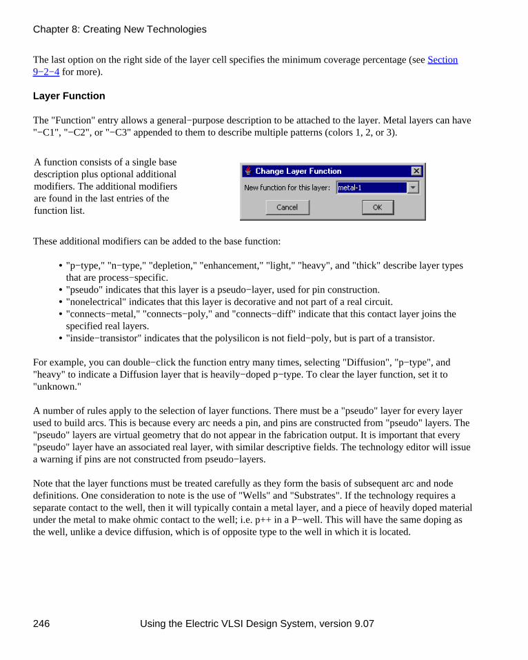
The last option on the right side of the layer cell specifies the minimum coverage percentage (see Section9−2−4 for more).
Layer Function
The "Function" entry allows a general−purpose description to be attached to the layer. Metal layers can have"−C1", "−C2", or "−C3" appended to them to describe multiple patterns (colors 1, 2, or 3).
A function consists of a single basedescription plus optional additionalmodifiers. The additional modifiersare found in the last entries of thefunction list.
These additional modifiers can be added to the base function:
"p−type," "n−type," "depletion," "enhancement," "light," "heavy", and "thick" describe layer typesthat are process−specific.
•
"pseudo" indicates that this layer is a pseudo−layer, used for pin construction. • "nonelectrical" indicates that this layer is decorative and not part of a real circuit. • "connects−metal," "connects−poly," and "connects−diff" indicate that this contact layer joins thespecified real layers.
•
"inside−transistor" indicates that the polysilicon is not field−poly, but is part of a transistor. •
For example, you can double−click the function entry many times, selecting "Diffusion", "p−type", and"heavy" to indicate a Diffusion layer that is heavily−doped p−type. To clear the layer function, set it to"unknown."
A number of rules apply to the selection of layer functions. There must be a "pseudo" layer for every layerused to build arcs. This is because every arc needs a pin, and pins are constructed from "pseudo" layers. The"pseudo" layers are virtual geometry that do not appear in the fabrication output. It is important that every"pseudo" layer have an associated real layer, with similar descriptive fields. The technology editor will issuea warning if pins are not constructed from pseudo−layers.
Note that the layer functions must be treated carefully as they form the basis of subsequent arc and nodedefinitions. One consideration to note is the use of "Wells" and "Substrates". If the technology requires aseparate contact to the well, then it will typically contain a metal layer, and a piece of heavily doped materialunder the metal to make ohmic contact to the well; i.e. p++ in a P−well. This will have the same doping asthe well, unlike a device diffusion, which is of opposite type to the well in which it is located.
Chapter 8: Creating New Technologies
246 Using the Electric VLSI Design System, version 9.07

Two rules apply here:
There must be a separate diffusion layer for the p++ or n++ used as a contact in a P−well or N−well,respectively; it cannot be the same layer that is used for diffusions in active devices.
1.
A p++ or n++ layer that is used to make a contact in a well of the same semiconductor type (forexample p++ in a P−well) must not be defined with the layer function Diffusion; it must be declaredas "Well". In the well contact shown below, both the p++ layer and the P−well layer will be definedwith the layer function "Well, P−type".
2.
Chapter 8: Creating New Technologies
Using the Electric VLSI Design System, version 9.07 247

8−5: The Arc Cells
Creating and Deleting Arc Cells
Arcs are the wires in a technology, and they are constructed from pieces of geometry on the layers. To edit anexisting arc, select it from the cell explorer or the Edit Cell... command (in menu Edit).
To create a new arc, use the context menu on the"TECHNOLOGY ARCS" entry of the cell explorerand choose "Add New Arc".
An arc can be deleted simply by deleting its cell. An arc can be renamed by renaming its cell, but rememberto use the name "arc−" in front (i.e. the old name is "arc−metal" and the new name is "arc−metal−1").Finally, you can rearrange the order in which the arcs will be listed with the "Reorder Arcs" command fromthe context menu.
Editing Special Arc Information
Arc cells show a sample arc on the bottom and a few pieces of textual information above it. The textualinformation can be updated by double−clicking on it.
"Function" describes the arc's function,which is a different set than the layerfunctions. As with layer functions, the arcfunctions should be carefully considered.
•
"Fixed−angle" lets you choose whether ornot default arcs of this type are drawn atfixed angles (see Section 5−2−1). In manylayout technologies, the correct state is "yes".The particular fixed angle is specified by the"Angle increment" field below.
•
"Wipes pins" lets you choose whether or not these arcs completely erase connecting pins (thesensible state is "yes" because pins are drawn in the same layer and would not be visible anyway).
•
"Extend arcs" lets you choose whether or not these arcs extend beyond their endpoints by half oftheir width (see Section 5−4−3). The typical state is "yes".
•
"Angle increment" is the preferred angle granularity of this type of arc (see Section 5−5).• The typical state is "90" which requests Manhattan arcs. "Antenna Ratio" is used in antenna rules calculations (see Section 9−3−2).•
Chapter 8: Creating New Technologies
248 Using the Electric VLSI Design System, version 9.07

A well arc that contains a well layer and does not contain device diffusion (i.e. opposite doping to the well)must not be defined as "diffusion"; it must be defined as "well−diffusion". This prevents the Spice extractorfrom incorrectly adding any p or n doped area found in the well arc to the source or drain area of a transistoron the same network. This does not mean that a device arc cannot contain a well layer. Device arcs will bedeclared as "p−diffusion" or "n−diffusion", and their well layer will be handled correctly; the arc connectivityis really defined by the device diffusion layer. For example, a p−device arc will have an N−well, or Nsubstrate under it, and a p−type diffusion will end up as part of the drain or source of the P transistor to whichit is connected.
Editing Arc Geometry
In addition to the above information, the arc must also be described with pieces of geometry on the variouslayers. Thus, a prototypical arc must be drawn in this cell. The length of the arc is not important, but thesmaller dimension is presumed to be the width and defines the default for this arc type.
Use the entries from the component menu of the sidebar to create new layers. The typical layer in an ICtechnology is a Filled box (third from the top).
After the geometry is created, it can be moved andresized with standard Electric commands. Rememberto keep all arc geometry separate from theinformation messages in the cell so that thetechnology editor can distinguish them. Once a pieceof geometry is created, its layer can be set bydouble−clicking on it. A menu is then presented withpossible layers (ignore the last entries,"SET−MINIMUM−SIZE", and"CLEAR−MINIMUM−SIZE" which are used onlyfor nodes).
Besides geometric layers, the graphical arcdescription must have a highlight layer to show wherethe arc will be outlined when used in a circuit.Although the highlighting is typically drawn aroundthe outside of all geometry, implant layers mayextend beyond the highlight (see the CMOS diffusionarcs for an example of this). Select the "HIGH" entryin the component menu to create this special type oflayer.
After geometry has been created, there may be some confusion as to what is there. To find out, use theIdentify Primitive Layers command (in menu Edit / Technology Editing), which temporarily labels eachpiece of geometry in the arc cell.
Chapter 8: Creating New Technologies
Using the Electric VLSI Design System, version 9.07 249
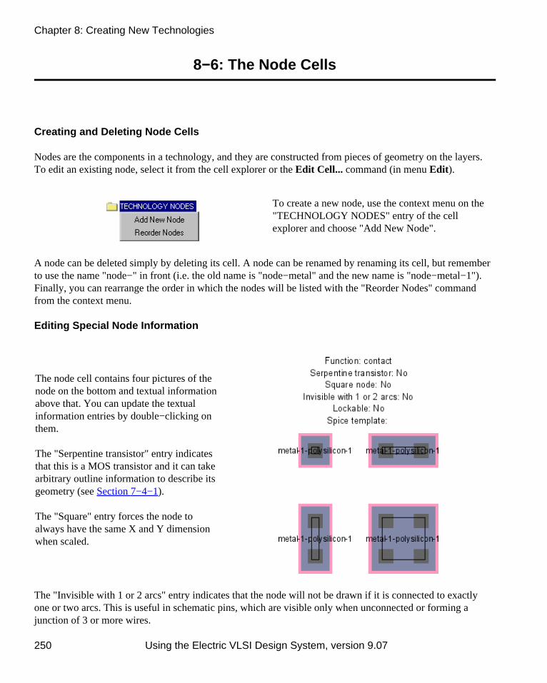
8−6: The Node Cells
Creating and Deleting Node Cells
Nodes are the components in a technology, and they are constructed from pieces of geometry on the layers.To edit an existing node, select it from the cell explorer or the Edit Cell... command (in menu Edit).
To create a new node, use the context menu on the"TECHNOLOGY NODES" entry of the cellexplorer and choose "Add New Node".
A node can be deleted simply by deleting its cell. A node can be renamed by renaming its cell, but rememberto use the name "node−" in front (i.e. the old name is "node−metal" and the new name is "node−metal−1").Finally, you can rearrange the order in which the nodes will be listed with the "Reorder Nodes" commandfrom the context menu.
Editing Special Node Information
The node cell contains four pictures of thenode on the bottom and textual informationabove that. You can update the textualinformation entries by double−clicking onthem.
The "Serpentine transistor" entry indicatesthat this is a MOS transistor and it can takearbitrary outline information to describe itsgeometry (see Section 7−4−1).
The "Square" entry forces the node toalways have the same X and Y dimensionwhen scaled.
The "Invisible with 1 or 2 arcs" entry indicates that the node will not be drawn if it is connected to exactlyone or two arcs. This is useful in schematic pins, which are visible only when unconnected or forming ajunction of 3 or more wires.
Chapter 8: Creating New Technologies
250 Using the Electric VLSI Design System, version 9.07

The "Lockable" entry indicates that this node can be made unchangeable along with other lockableprimitives, when the lock is turned on during editing (see Section 6−2 for more on locking these primitives).This is typically used in array technologies such as FPGA (see Section 7−6−2).
The "Spice template" entry is an overriding line of Spice code to be emitted for this primitive. See Section9−4−4 for more on Spice templates.
The "Function" entry describesthe node's function, which is adifferent set than the arc andlayer functions. A dialog offers alist of possible node functions.
Editing Node Geometry
For nodes, it is common to sketch four different examples of the node in varying scales, so that X and Yscaling rules can be derived (square nodes need only two examples). If only one example is specified, linearscaling rules will be presumed.
The smallest example, called the main example, is used as the default size and also contains all of the specialport information. Needless to say, it is important to keep the geometry of each example well apart from theothers so that the technology editor can distinguish them.
Each example must contain the same geometric layers (only stretched). As in the Arc cells, pieces ofgeometry can be created by selecting from the component menu of the side bar, creating the geometry, andthen double−clicking to assign a layer. If any polygonal geometry is used (for example, the Filled polygonentry, sixth from the top), they require outline information to be assigned (see Section 6−10−1). If theOpened circle arc entry is selected (second from the bottom), you can specify the number of degrees of thecircle with the Object Properties... command (in menu Edit / Properties).
Each example must also contain a highlight layer to indicate the correct highlighting on the display. Selectthe "HIGH" entry from the component menu to create this special type of layer.
Each example must also contain port information. Select the "PORT" entry in the component menu to createthis special type of layer. You will have to provide a name for each port, and the name must be the same oneach example.
Chapter 8: Creating New Technologies
Using the Electric VLSI Design System, version 9.07 251

Ports on the main example must also haveconnectivity information (which arcs canconnect to them) and range information (thepermissible angle of connected arcs).Double−click on the port to set this.
The range consists of two numbers: an angle(in degrees counterclockwise from 3 O'clock)and an angle range. For example, a port angleof 90 with a port angle range of 45 describes aport that points upward and can connect atangles up to 45 degrees off from this direction.The range will be graphically depicted.
The ports on the main example must also indicate any internal electrical connectivity by actually connectingthem together. For example, the two polysilicon ports on a MOS transistor should be connected in the mainexample. Join the ports with a universal arc. Do not put this internal connection on any example other thanthe main one. To see the location of all ports on the main example, use the Identify Ports command (inmenu Edit / Technology Editing).
For simple nodes, such as pins and contacts, there is typically one port which is in the center of the node.However, some of Electric's built−in technologies give these ports a nonzero size. The idea behind doing thisis to allow arcs to "slide" within that port (see Section 5−2−2). Many disagree with the idea of havingnonzero ports on pin nodes, and so it is now recommended that all pin nodes have zero size ports.
As with arcs, use the Identify Primitive Layers command to label each piece of geometry in the mainexample.
Chapter 8: Creating New Technologies
252 Using the Electric VLSI Design System, version 9.07

Node Variations
It is sometimes the case that two or more primitive nodes are nearly the same and differ only by the shape oftheir layers. When this happens, it is possible to define them all in the same cell using the notion ofvariations. To create a variation on a node, create a 5th example in the cell (for two variations, create a 5thand 6th example). Each variation example must follow these rules:
It must have the same layers as themain four examples. Variations are notable to add or remove layers...this isdone by creating separate nodes.
•
A central node must be named. Pickany piece of geometry that is centeredin the example (contact cuts are goodchoices). This piece of geometry mustbe named (using the ObjectProperties... command in menu Edit /Properties). The name on the piece ofgeometry will be the name of thevariation.
•
The only rule used to compute layer size is the distance from the outer edge. It is not possible to useother stretching rules because only one example is being provided.
•
The picture shown here illustrates a variation in which the polysilicon layer is inset. The text "Small−Poly" isthe name of the cut node (moved up to make it readable).
Special Node Considerations
There are some special cases available in node descriptions. A piece of geometry in the main example maybe changed (by double−clicking on its function) to "SET−MINIMUM−SIZE". This indicates that the currentsize is the smallest possible, and it cannot scale any smaller (this is used by the "mocmos" technology for themetal layer in contacts). The restriction can be removed with the "CLEAR−MINIMUM−SIZE" description.This option cannot be used in serpentine transistors.
Another special case in node description is the ability to specify multiple cut layers. If the larger exampleshave more cut layers, rules are derived for cut spacing and indentation so that an arbitrary numbers of cutscan be inserted as the contact scales.
Although serpentine MOS transistors are a special case, they cannot be automatically identified, but must beexplicitly indicated with a textual indicator. Besides this explicit indication, the transistor node must containfour ports: two on the gate layer (polysilicon) and two on the gated layer (active). A standard geometry mustbe used that shows polysilicon and diffusion crossing in a central transistor area. Any deviation from thisformat may cause the technology editor to be unable to derive serpentine rules for the node.
Chapter 8: Creating New Technologies
Using the Electric VLSI Design System, version 9.07 253

Besides the standard nodes for transistors, contacts, and other circuit elements, it is necessary to build pin andpure−layer nodes. There should be one pin for every arc, so that the arc can connect to others of its type. Thepin should be constructed of pseudo−layers (i.e. it has no real geometry), should have the "pin" function, andshould have one port in the center that connects to one arc. The technology editor will issue a warning ifthere is no pin node associated with an arc.
The pure−layer nodes should also be built, one for each layer. They should have only one piece of geometryand have the "pure−layer" function. The technology editor will issue a warning if there is no pure−layer nodeassociated with a layer.
Chapter 8: Creating New Technologies
254 Using the Electric VLSI Design System, version 9.07

8−7: Miscellaneous Information
The Support Cell
Each cell in a technology library describes a different aspect of the technology. The support cell containstechnology−wide information. To see this, edit the cell "factors" under the "TECHNOLOGY SUPPORT"section of the cell explorer.
The support cell contains many items, any of which can be changed by double−clicking on it.
"Scale" is the scaling factor between grid units and nanometers.• "Description" is the full description of the technology.• "Minimum Resistance" is the minimum resistance for the technology (see Section 9−10−1 for thisand other parasitics).
•
"Minimum Capacitance" is the minimum capacitance for the technology.• "Gate Shrinkage" is the gate shrinkage for the technology.• "Gates Included in Resistance" tells whether to include a transistor's gate in resistance computations.• "Parasitics Includes Ground" tells whether to include ground networks in parasitics computations.•
Transparent Colors
Double−clicking on the "TransparentColors" entry shows a dialog forselecting the transparent colors. Youmust define as many colors as youhave used in the layers.
Chapter 8: Creating New Technologies
Using the Electric VLSI Design System, version 9.07 255

Design Rules
Unfortunately, it is not possible to edit design rules associated with the technology. However, you can adddesign rules to the XML files produced by the technology editor. To do this, examine the XML files for someexisting technologies (for example, CMOS) and copy these lines to the new XML file, editing whereappropriate for layer names and spacings.
The Component Menu
To customize thelayout of thecomponent menu, usethe Edit ComponentMenu... command (inmenu Edit /Technology Editing).This dialog worksexactly the same asthe Component MenuPreferences (seeSection 4−5−1).
Chapter 8: Creating New Technologies
256 Using the Electric VLSI Design System, version 9.07

8−8: How Technology Changes Affect Existing Libraries
Once a technology is created, the components are available for design. Soon there will be many libraries ofcircuitry that makes use of this new technology. What happens to these libraries when the technologydescription changes? In most cases, the change correctly affects the existing libraries. However, somechanges are more difficult and might invalidate the existing libraries. This section discusses the possiblechanges and shows workarounds for the difficult situations.
Technology information appears in four different places: the layers, the arcs, the nodes, and miscellaneousinformation on the technology (the support cell and color tables). Information in these areas can be added,deleted, or modified. The rest of this section outlines all of these situations.
Adding layers, arcs, nodes, and miscellaneous information
Adding information has no effect on the existing circuitry. All subsequent circuit design may make use of thenew technology elements.
Deleting layers, nodes, arcs, and miscellaneous information
All references to a deleted layer, in any nodes or arcs of the technology, will become meaningless. This doesnot invalidate libraries that use the layers, but it does invalidate the node and arc descriptions in thetechnology. The geometry in these nodes and arcs will have to be moved to another layer.
Deleting nodes or arcs will cause error messages when libraries are read that make use of the deleted objects.When the library is read, you can substitute another node or arc to use in place of the now−unknowncomponent.
Deleting miscellaneous information depends entirely on where that information is removed. For example, ananalysis tool may fail to find the information that it requires.
Modifying layers, nodes, arcs, and miscellaneous information
Modifying layers is a totally transparent operation. Any change to the color, style, or stipple information(including changes to the color map) will appear in all libraries that use the technology. Changes to I/Oequivalences or Spice parasitics will be available to all existing libraries. A change of the layer function mayaffect the technology editor's ability to decode the nodes and arcs that use this layer (for example, if youchange the function of the "polysilicon" or "diffusion" layers that form a transistor, the editor will be unableto identify this transistor). Renaming a layer has no effect.
Modifying arcs and nodes is not as simple as layer modification because the arcs and nodes appear in thecircuit libraries, whereas the layers do not. If you rename a node or arc, it will cause errors when libraries areread that make use of nodes with the old name. Therefore, you must create a new node or arc first, convert allexisting ones to the new type, and then delete the old node or arc.
Chapter 8: Creating New Technologies
Using the Electric VLSI Design System, version 9.07 257

Many of the pieces of special information on the top of the node and arc cells apply to newly createdcircuitry only, and do NOT affect existing components already in libraries. The arc factors "Fixed−angle","Wipes pins", "Extend arcs", and "Angle increment" have no effect on existing libraries. The node factor"Square node" also has no effect on existing circuitry and gets applied only in subsequent designs.
Other factors do affect existing circuitry. Changes to the "Function" field, in both arcs and nodes, pass to allexisting components, thus affecting how analysis tools treat the old circuits. If the "Serpentine Transistor"field in nodes is turned off, any existing transistors that have serpentine descriptions will turn into largerectangular nodes with incorrect connections (i.e. get trashed). Unfortunately, it may become impossible tokeep the "Serpentine Transistor" field on if the geometry does not conform to standards set by the technologyeditor for recognizing the parts. If a node is not serpentine, turning the factor on has no effect. Finally, thenode factors "Invisible with 1 or 2 arcs" and "Lockable" correctly affect all existing circuitry.
A more common modification of arcs and nodes is to change their graphical descriptions. A simple ruleapplies to all such changes: the size of existing nodes and arcs is the amount that their highlighted area islarger than the default highlighted area. Thus, an arc or node that is at its default size will be saved with azero size increase. If you change the default size, it will make all default−sized nodes and arcs change aswell. If the node is larger than the default size, it will grow accordingly.
For example, assume thatan arc has a default widthof 2, and there are two ofthese arcs, one that is 2wide (an increase of 0beyond the default) andone that is 3 wide (anincrease of 1 beyond thedefault). If you redefine the technology such that these arcs are now 4 wide by default, then the old 2−wide arcbecomes 4 wide and the old 3−wide arc becomes 5 wide.
Because of these changes, it may be preferable to keep the old technology and give the new technology adifferent name. Then the old libraries can be read into the old technology, and the Make Alternate LayoutView... command (in menu View) can be used to translate into the new technology. This command uses nodeand arc functionality to associate components, scaling them appropriately relative to their default sizes. Thechange is completed by deleting the old technology, renaming the new technology to the old name, and thensaving the library.
Finally, modifying miscellaneous information is typically transparent: changed information appears in allexisting libraries, and affects those subsystems that make use of the information. For example, a change tothe Spice resistance will be seen when a Spice deck is next generated.
Chapter 8: Creating New Technologies
258 Using the Electric VLSI Design System, version 9.07

8−9: Examples of Use
To fully understand technology editing, some examples are appropriate. Two examples will be given: asimple one that modifies the appearance of a pattern, and a more complex example in which a new primitivenode is created. Both examples are based on the MOSIS CMOS technology, so they presume that theConvert Technology to Library for Editing... command (in menu Edit / Technology Editing) has beenissued and the "mocmos" entry was selected.
Example: Modifying a Layer's Appearance
In this first example, the user simply wishes to change the Metal−2 layer from a solid fill to a stipple pattern.
This particular task is so basic that it can be done with the Layers Preferences, but it illustrates the basic stepsof making a change. First, edit the layer cell for "metal−2". The display will show the layer with all of itsassociated information.
Because every layer has a default stipple pattern used for printing, all that is necessary is to change the"Style" field from solid to patterned. To do this, double−click on the "Style" text and select"Patterned/Outline=None". The technology is now modified and can be converted back with the ConvertLibrary to Technology... command.
Chapter 8: Creating New Technologies
Using the Electric VLSI Design System, version 9.07 259

Example: Creating a New Node
The second example is more extensive: creation of a new primitive node. In this case, the new node is acontact between metal−2 and polysilicon.
To create the node, use the context menuon the "TECHNOLOGY NODES" tab ofthe explorer window, select "Create NewNode", and name the node appropriately.
At this point, the display will show only the textual information about the node (because the graphicalinformation is yet to be supplied). The textual information consists of five factors that now fill the screen.
You should begin by changing the"Function" factor to "contact"(double−click it and select the appropriatefunction). Then pan back so there is roomto describe the node graphically. The otherfactors are properly set for a contact.
To place a piece of geometry (forexample, some polysilicon), click overthe Filled Box entry in the componentmenu (third from the top) and thenclick in the edit window. Thisgeometry now has shape, but no layerassociated with it. To assign a layer,double−click on the geometry. Thenchoose "polysilicon−1". The blackbox will change appearance to that ofa polysilicon layer. You can move andstretch this box appropriately.
In this example, assume that a contact between polysilicon and metal−2 has three layers: polysilicon−1,metal−2, and contact cut. Therefore, the above operation must be done two more times to place the metal−2and contact cut layers.
Chapter 8: Creating New Technologies
260 Using the Electric VLSI Design System, version 9.07

Besides this pure geometry, there must be two other items in the node: a highlight layer and a port. Thehighlight layer is obtained by selecting the "HIGH" entry from the component menu. It is then placed andstretched so that it encloses the contact (highlight layers define the size of the node, and this means that theywill typically surround the geometry).
The other item that must be created is a port(more than one can be created, but forcontacts, one is sufficient). Select the"PORT" entry from the menu on the left andplace it in the display. You will be promptedfor a port name, after which you can furthermove or stretch the port. Besides a locationand a name, ports must specify which arcsmay connect to them. To do this,double−click on the port.
The resulting menu lists all of the arcs andindicates possible connectivity. Note thatthe last two entries define the permissiblerange of angles to which arcs may connect.For a contact such as this, arcs may connectat any angle, so the default values arecorrect.
When all of the geometry, highlighting, andports have been placed, you candouble−check your work with the IdentifyPrimitive Layers command (in menu Edit/ Technology Editing), which will displaythis information (note that the port name"Center" has been moved away for clarity):
The final step in the definition of this node is to create three more copies that illustrate scaling in both axes.This is done simply by selecting all five objects and using the Duplicate command (in menu Edit). Onceduplicated in a new location, each piece must be stretched appropriately. In this example, the contact cut isdesigned so that the number of cut elements grows with the node. Thus, when stretched horizontally orvertically, there are two cuts, and when stretched in both directions there are four cuts. The technology editorwill determine precise multicut rules from the cut spacing and the amount of stretch, so that even more cutswill appear as the node grows larger. The finished node definition is shown below. All that is necessary is toconvert this library back to a technology, and the new technology will have this node.
Chapter 8: Creating New Technologies
Using the Electric VLSI Design System, version 9.07 261

Of course, the newly created technology is valid only during the current session. Therefore, to preserve thistechnology, write XML and add it to the Added Technologies Preferences.
Chapter 8: Creating New Technologies
262 Using the Electric VLSI Design System, version 9.07

8−10: Technology XML File Format
Introduction
Layout technologies in Electric can be described by Xml technology files. These files are automaticallygenerated by the technology editor and the technology−creation wizard, but some users may prefer to editthem by hand. For these users, the following is a description of the technology XML file format.
Electric currently has Xml technology files that are unparameterized (all values are explicitly entered andthere is no symbolic information). Technology distances are specified as double−precision numbers indisplay units. Future versions of Electric may implement a symbolic style of Xml technology files.
Currently technology files contain two kinds of information:
Electric−independent information. This includes physical and electrical details of the foundryprocess. Most of these details are attached to Layers and includes design rules, simulationinformation, etc.
1.
Electric−specific information. This includes the primitive nodes and arcs that Electric uses fordesign. It also has connectivity rules, display and print styles, component menus for the technology,etc.
2.
Primitive nodes and arcs can be considered to be layout macros. Node description consists of a set oftwo−dimensional shapes. Arcs description consists of a set of one−dimensional intervals, which are stretchedin the other dimension. The technology file describes primitive nodes and arcs of a standard size (usually theDRC minimum) and also includes information about how they can grow larger. Instances of these nodes andarcs in Libraries can be larger than standard.
A primitive node or arc can consists of many shapes in different technology Layers. Each shape in aprimitive node is called a NodeLayer. Each interval in a primitive arc is called an ArcLayer.
The minimum bounding box of all NodeLayers of a primitive node is called its FullRectangle. Descriptionof a primitive node can also define the FullRectangle explicitly. The largest of all ArcLayers in a primitivearc defines its FullWidth.
Primitive nodes and arcs also have the notion of a BaseRectangle and a BaseWidth. They relate to the shapeof the most important layer in this node or arc. The BaseRectangle of a primitive node is described explicitly.The BaseWidth of primitive arc is the width of the first 'ArcLayer' in the arc description. The BaseRectangleand BaseWidth are highlighted in the Edit Window and they appear in Properties dialogs.
Instances of nodes and arcs in a library can have sizes larger than standard. Electric writes size information ofeach instance in the library files. Since release 8.05 of Electric (or more precisely since the 8.05odevelopment version) library files contain the extent of the node/arc over its standard size described in the
Chapter 8: Creating New Technologies
Using the Electric VLSI Design System, version 9.07 263
technology file. When you switch a design library from one technology to another compatible technology,the standard size node/arc in old technology is converted to the standard size node/arc in the new technology.The node/arc which extends by 1 unit beyond the standard node/arc in old technology is converted to anode/arc which extends by 1 unit beyond the standard node/arc in new technology.
Older Electric releases wrote sizes of node/arc instances in another way. Jelib format before Electric 8.05(actually, the 8.05g development version) and all Elib files saved the size of the FullRectangle andFullWidth. Jelib format between 8.05g and 8.05n wrote sizes of BaseRectangle and BaseWidth. The Full andBase sizes can be redefined in future versions of technology file. To be able to read older Jelib formatscorrectly after redefinition of Full and Base, Technology file can contain explicit sizes of standard nodes andarcs in older library files.
All sizes in technology files are in display units. There is a scale declaration which relates this unit tonanometers.
Overall Structure
Here is a description of Xml technology file in Electric releases 8.05 and 8.06.
<technology> is the main element of the Xml technology file. It has many Xml−specific attributes:
"name" contains the name of this technology inside Electric. • "class" (optional) contains the name of a Java class which is a subclass of"com.sun.electric.technology.Technology". It can be used to describe things which are not describedby the Xml technology class yet. The interface with this class is not specified and can be changed. Ifyou need a non−standard technology feature, the better way is to contact Electric developers aboutthis.
•
Example: <technology name="mocmos" class="com.sun.electric.technology.technologies.MoCMOS" xmlns="http://electric.sun.com/Technology" xmlns:xsi="http://www.w3.org/2001/XMLSchema−instance" xsi:schemaLocation="http://electric.sun.com/Technology ../../technology/Technology.xsd">
Inside of the <technology> element are these subelements:
<shortName> a more descriptive name for the technology (optional) • <description> the most descriptive name for the technology. • <version> describes Electric versions when Jelib changed and how it affects sizes. The "tech"attribute contains an identifier of this version used in subsequent <diskOffset> subelements of<arcProto> and <primitiveNode> descriptions. The "electric" attribute is a corresponding Electricversion. These elements are usually fixed in all technology files.Examples: <version tech="1" electric="8.05g"/> <version tech="2" electric="8.05o"/>
•
Chapter 8: Creating New Technologies
264 Using the Electric VLSI Design System, version 9.07

<numMetals> describes a possible range for the number of metall layers in the technology. There isno good support for Xml technology files with a variable number of metal layers. Therefore, thiselement should contains the same value for all three attributes.Example: <numMetals min="6" max="6" default="6"/>
•
<scale> defines how many nanometers are in a display unit. Electric uses dimensionless "units" in itsinterface, where a transistor may be "2x3" without specifying actual distances. This scale convertsthe units to real spacings. The "relevant" attribute should be true for layout technologies.Example: <scale value="200.0" relevant="true"/>
•
<resolution> defines the minimum resolution value in grid units used in DRC, a parameter todetermine which points are off−grid.Example: <resolution value="2.0"/>
•
<defaultFoundry> is a name of the default foundry for this technology. The name references one ofthe <foundry> elements found later in the Xml file.Example: <defaultFoundry value="MOSIS"/>
•
<minResistance> global minimum resistance (for parasitics).Example: <minResistance value="4.0"/>
•
<minCapacitance> global minimum capacitance (for parasitics).Example: <minCapacitance value="0.1"/>
•
<logicalEffort> defines default project preferences for the Logical Effort tool.Example: <logicalEffort gateCapacitance="0.167" wireRatio="0.16" diffAlpha="0.7"/>
•
<transparentLayer> defines the transparent layers in the technology. All layers can be drawn ineither a "transparent" or "opaque" style. Transparent layers can overlap other transparent layerswithout obscuring each other (they blend where they overlap). Opaque layers cover all other layerswithout blending. Because the system needs to store all combination of transparent layers, it is notpossible to make every layer transparent. Instead, less−used layers should be opaque and use astipple−pattern so that they do not cover everything. The exception is the Layer−DisplayAlgorithm which does not use the transparent/opaque distinction (see Section 4−3 for more on thedisplay algorithms). This element lists the number of transparent layers, and provides the color ofeach. The system automatically determines the blending colors where multiple transparent layersoverlap.Example: <transparentLayer transparent="1"> <r>96</r> <g>209</g> <b>255</b> </transparentLayer>
•
<layer> a list of layer descriptions (see below). • <arcProto> a list of primitive arc descriptions (see below). • <primitiveNode/primitiveNodeGroup> a list of primitive node and primitive node group•
Chapter 8: Creating New Technologies
Using the Electric VLSI Design System, version 9.07 265

descriptions (see below). <spiceHeader> default spice models. • <menuPalette> description of the default component menu (optional). • <foundry> information for the Foundry. Each has default DRC rules and default GDS mapping. •
Layers
The <layer> elements define layers in the technology. They contains these attributes:
"name" the name of this layer. Layer names are not referenced in Library files. They are used onlyin the description of primtive nodes and arcs and in DRC rules.
•
"fun" the function of this layer, taken from this list: UNKNOWN METAL1 ... METAL12 (metal) METAL1C1 ... METAL12C1 (metal) METAL1C2 ... METAL12C2 (metal) METAL1C3 ... METAL12C3 (metal) POLY1 ... POLY3 (polysilicon) GATE (gate polysilicon) DIFF DIFFP DIFFN (active) IMPLANT IMPLANTP IMPLANTN SUBSTRATE WELL WELLP WELLN (implants) CONTACT1 ... CONTACT12 (cuts) RESISTOR CAP (resistor/capacitor) TRANSISTOR (transistor) EMITTER BASE COLLECTOR (bipolar parts) DMY* DEXCL* (dummy and dummy−exclusion for different layers) BUS ART (schematics and artwork) PLUG OVERGLASS GUARD ISOLATION (specialty) TILENOT CONTROL (specialty)
•
"extraFun" optional functions for this layer, taken from this list: nonelectrical connects−metal connects−poly connects−diff heavy light depletion_heavy depletion_light enhancement_heavy enhancement_light vt thick native inside_transistor deep carb−nano n−type deprecated: use fun=IMPLANTN p−type deprecated: use fun=IMPLANTP
•
Example: <layer name="Poly−Cut" fun="CONTACT1" extraFun="connects−poly">
Inside of the <layer> element are these subelements:
<transparentColor> the transparent color to use (if omitted, this is an opaque layer). • <opaqueColor> the opaque color to use. • <patternedOnDisplay> true to use the <pattern> when drawing on the screen. •
Chapter 8: Creating New Technologies
266 Using the Electric VLSI Design System, version 9.07

<patternedOnPrinter> true to use the <pattern> when printing. • <pattern> the stipple pattern to use (if requested on either the screen or printed page). • <outlined> true to outline the layer (sensible only for patterned layers). • <opacity> intensity of this layer (from 0 to 1). • <foreground> true to place this layer in the foreground. • <display3D> defines thickness and height above the substrate for 3D display and parasitics. Theelement has these attributes:
"thick" 3D thickness of the layer in display units ♦ "height" 3D height of the bottom of the layer in display units ♦ "mode" 3D display style ♦ "factor" 3D display style ♦
Example: <display3D thick="0.75" height="15.75" mode="NONE" factor="0.2"/>
•
<cifLayer> CIF layer name. • <skillLayer> Skill layer name. • <parasitics> parasitic extractor subelements. • <pureLayerNode> description of the pure−layer node for this layer. This node is used to representarbitrary polygons of this Layer. It is also used when importing from external formats like GDS. Thestandard pure−layer node has zero FullRectangle and BaseRectangle. So library files contain exactgeometric information for instances of pure−layer node. All the shape of pure−layer node isconsidered a port shape of the single port of the node. There are these optional subelements:
<oldName> if the pure−layer node has another name in older versions of the technology. ♦ <lambda> the default width of this pure−layer−node (in grid units) when it is placedmanually.
♦
<portArc> the list of arc names which can connect to this pure−layer node. ♦ Example: <pureLayerNode name="Transistor−Poly−Node" port="trans−poly−1"> <lambda>2.0</lambda> <portArc>Polysilicon−1</portArc> </pureLayerNode>
•
Chapter 8: Creating New Technologies
Using the Electric VLSI Design System, version 9.07 267

Arcs
<arcProto> elements describe primitive arcs in the technology. They have these attributes:
"name" is the name of the arc prototype. The instances of the primitive arc in Electric librariesreference this name.
•
"fun" describes the arc function: UNKNOWN METAL1 ... METAL12 (metal) POLY1 ... POLY3 (polysilicon) DIFF DIFFP DIFFN DIFFS DIFFW (active) BUS (busses) UNROUTED (unrouted, for routers) NONELEC (non−electrical, for constraints)
•
Example: <arcProto name="P−Active" fun="DIFFP">
Inside of the <arcProto> element are these subelements:
<oldName> the name of this primitive arc in previous versions of the technology (optional). • <wipable> flag to mark that the arc erases its pins. This flag is usually present in layouttechnologies.
•
<curvable> flag to described round arcs. It is not supported in the current implementation. • <special> flag related to the component menu. • <skipSizeInPalette> flag related to the component menu. • <notUsed> flag to forbid use of this primitive arc in libraries. • <extended> default state of end−extension for this arc. • <fixedAngle> default state of the fixed−angle constraint on this arc. • <angleIncrement> default state of the angle−increment amount on this arc (grids placement angles). • <antennaRatio> value used by the ERC tool. • <diskOffset> tells how sizes were written in older library files. The attribute "untilVersion"references the "tech" attribute of the <version> element above. This disk offset is applied to Jeliblibraries with Electric versions prior to the "electric" attribute of that <version> element. Attribute<width> is actually half of the value written to Jelib file. For example, the "P−Active" arc describedabove will be: 15.0 wide with Jelib prior to Electric version "8.05g"; 3.0 wide with Jelib prior to Electric version "8.05o"; 0.0 wide with Jelib in Electric versions since "8.05o".More formally, let a.extend be the internal value associated with the arc instance in the Electricdatabase. The value written to libraries prior to "diskOffset.untilVersion" was 2*(a.extend +diskOffset.width). The <diskOffset> element is necessary only in legacy technologies.Example: <diskOffset untilVersion="1" width="7.5"/>
•
<defaultWidth> factory default value of arc width. This element is not used now and should beomitted.
•
Chapter 8: Creating New Technologies
268 Using the Electric VLSI Design System, version 9.07

<arcLayer> a list of ArcLayers that comprise this Arc. The attribute "layer" references the layer ofthe ArcLayer. The attribute "style" is either "FILLED" or "CLOSED". Layout arcs should be"FILLED". The <lambda> subelement describes extent (half width) of the ArcLayer from the centralline of the arc.More formally, let a.extend be the internal value associated with the arc instance in the Electricdatabase. The width of the "P−Select" <arcLayer> below is 2*(a.extend + 3.5) The FullWidth of thearc instance is the width of the widest ArcLayer. It is 2*(a.extend + 7.5) in the above "P−Active" arc.The BaseWidth of the arc instance is the width of the first ArcLayer in the list. It is 2*(a.extennd +1.5) in the above "P−Active" arc.Example: <arcLayer layer="P−Select" style="FILLED"> <lambda>3.5</lambda> </arcLayer>
•
Example: <arcProto name="P−Active" fun="DIFFP"> <wipable/> <extended>true</extended> <fixedAngle>true</fixedAngle> <angleIncrement>90</angleIncrement> <antennaRatio>200.0</antennaRatio> <diskOffset untilVersion="1" width="7.5"/> <diskOffset untilVersion="2" width="1.5"/> <arcLayer layer="P−Active" style="FILLED"> <lambda>1.5</lambda> </arcLayer> <arcLayer layer="N−Well" style="FILLED"> <lambda>7.5</lambda> </arcLayer> <arcLayer layer="P−Select" style="FILLED"> <lambda>3.5</lambda> </arcLayer> </arcProto>
Chapter 8: Creating New Technologies
Using the Electric VLSI Design System, version 9.07 269
Nodes
<primitiveNode> elements describe primitive node in the technology. They have these attributes:
"name" is the name of the node prototype. Instances of this primitive node in Electric librariesreference this name.
•
"fun" describes the node function: UNKNOWN PIN (pins connect arcs) NODE (pure layer nodes) CONTACT CONNECT (nodes that connect all arcs) TRANMOS TRAPMOS TRA4NMOS TRA4PMOS (CMOS transistors) TRADMOS TRA4DMOS (nMOS transistors) TRANPN TRAPNP TRA4NPN TRA4PNP (Bipolar transistors) TRANJFET TRAPJFET TRA4NJFET TRA4PJFET (JFET transistors) TRADMES TRAEMES TRA4DMES TRA4EMES (MESFET transistors) TRANS TRANS4 (generic transistors) TRANSREF (reference transistors) RESIST PRESIST WRESIST ESDDEVICE (resistors) CAPAC ECAPAC (capacitors) DIODE DIODEZ (diodes) INDUCT (inductors) METER (meters) BASE EMIT COLLECT (Bipolar transistor parts) BUFFER GATEAND GATEOR GATEXOR (logic gates) FLIPFLOPRSMS FLIPFLOPRSP FLIPFLOPRSN (RS flipflops) FLIPFLOPJKMS FLIPFLOPJKP FLIPFLOPJKN (JK flipflops) FLIPFLOPDMS FLIPFLOPDP FLIPFLOPDN (D flipflops) FLIPFLOPTMS FLIPFLOPTP FLIPFLOPTN (T flipflops) MUX (multiplexors) CCVS CCCS VCVS VCCS TLINE (two−port gates) CONPOWER CONGROUND SOURCE (power/ground) SUBSTRATE WELL (implants) ART (artwork) ARRAY (array nodes) ALIGN (alignment nodes)
•
Example: <primitiveNode name="Metal−1−Metal−2−Con" fun="CONTACT">
Inside of the <primitiveNode> element are these subelements:
<oldName> optional name of this primitive node in previous versions of the technology. • <shrinkArcs> flag to shrink arcs connected to the node. This flag should be "on" only for PINnodes.
•
<square> flag to restrict the node to be square. It is used in round layout technologies. •
Chapter 8: Creating New Technologies
270 Using the Electric VLSI Design System, version 9.07

<canBeZeroSize> flag to allow the size to become zero (not used in layout technologies). • <wipes> flag which is not used in layout technologies. • <lockable> flag which is used in arrayed technologies (like FPGA). • <edgeSelect> flag which is not used in layout technologies. • <skipSizeInPalette> flag related to the component menu. • <notUsed> flag to forbid use of this primtive node in libraries. • <lowVt> flag to mark a low vt transistor. • <highVt> flag to mark a high vt transistor. • <nativeBit> flag to mark a native transistor. • <od18> flag to mark an od18 transistor. • <od25> flag to mark an od25 transistor. • <od33> flag to mark an od33 transistor. • <diskOffset> tells how sizes were written in older library files. It has this attribute:"untilVersion" references the "tech" attribute of <version> elements above. This disk offset is appliedto Jelib libraries with Electric version prior to "electric" attribute of that <version> element.Attributes <x> and <y> are actually half of the values written to Jelib file. So the"Metal−1−Metal−2−Con" node example shown below will be written: 5.0 width/height with Jelib prior to Electric version "8.05g"; 4.0 width/height with Jelib prior to Electric version "8.05o"; 0.0 width/height with Jelib in Electric versions since "8.05o".More formally, let n.extendX and n.extendY be the internal values associated with the node instancein the Electric database. The values written to library prior to "diskOffset.untilVersion" were
2*(n.extendX + diskOffset.x) and 2*(n.extendY + diskOffset.y).The <diskOffset> element is necessary only with legacy technologies.Example: <diskOffset untilVersion="1" x="2.5" y="2.5"/>
•
<defaultWidth> and <defaultHeight> factory default values of the node size. The subelement<lambda> contains the value of extendX/extendY in display units. Usually these elements areomitted because the default values of extendX and extendY are 0. So, the factory defaults of extendXand extendY are defaultWidth.lambda and defaultHeight.lambda The factory defaults of BaseWidthand BaseHeight are
BaseRectangle.width + 2*defaultWidth.lambdaand
BaseRectangle.height + 2*defaultHeight.lambda .The factory defaults of FullWidth and FullHeight are
FullRectangle.width + 2*defaultWidth.lambdaand
FullRectangle.height + 2*defaultHeight.lambda .
•
<nodeBase> defines the BaseRectangle of the node. It has a subelement <box> which has in it asubelement <lambdaBox>. In the <lambdaBox>, the attributes "klx", "khx", "kly", and "khy" are thecoordinates of the base rectangle of a standard−size node.
•
<sizeOffset> is deprecated. • <protection> defines the protection frame of the cell. • <nodeLayer> a list of NodeLayers (described below). • <primitivePort> a list of primitive ports on the node. The "name" attribute describes the port name.•
Chapter 8: Creating New Technologies
Using the Electric VLSI Design System, version 9.07 271

To make a library conversion from one technology to another it would help to unify port names insome manner. Port names of single−port nodes are not very important because the library reader canunambiguously connect arcs to the renamed port. However, port names of transistors could havecompatible names like "poly−top", "poly−bottom", "diff−left", "diff−right". <primtivePort> has thesesubelements:
<portAngle> can restrict direction of arcs which can connect to this port ♦ <portTopology> is a small integer that is unique among PrimitivePorts on thePrimitiveNode. When two PrimitivePorts have the same topology number, it indicates thatthese ports are connected.
♦
<box> a rectangle which constraints the position of end point of connected arc ♦ <portArc> a list of primitive arcs from this technology which can connect to this port ♦
Example: <primitivePort name="metal−1−metal−2"> <portAngle primary="0" range="180"/> <portTopology>0</portTopology> <box> <lambdaBox klx="−1.0" khx="1.0" kly="−1.0" khy="1.0"/> </box> <portArc>Metal−1</portArc> <portArc>Metal−2</portArc> </primitivePort>
<serpTrans> marks this node as serpentine transistor. It supplies 6 special values. • <polygonal> marks that this node can be an arbitrary polygon. Usually is not used in layouttechnologies.
•
<minSizeRule> overrides the FullRectangle of the node and supplies the name of a minimal sizerule The attributes "width" and "height" describe the size of the FullRectangle. The attribute "rule" isthe name of minimal size rule. By default the FullRectangle is calculated as the minimum boundingbox of all points found in the NodeLayers of a standard primitive node. For the"Metal−1−Metal−2−Con" node example shown below, the FullRectangle is calculated as a box withendpoints
[x = −2.0, y = −2.0] and [x = 2.0, y = 2.0].The FullBox of a node instance with n.extendX and n.extendY is:
[x = FullRectangle.minX − n.extendX, y = FullRectangle.minY − n.extendY]and
[x = FullRectangle.maxX + n.extendX, y = FullRectangle.maxY + n.extendY]This may be not accurate if shapes which made the minimum bounding box of the standard−sizenode grows more slowly than other shapes when extents are increased. The <minSizeRule> elementdefines the FullRectangle manually as a rectangle with its center at the origin. The FullRectangle inthe presence of <minSizeRule> is
[x = −0.5*minSizeRule.width, y = −0.5*minSizeRule.height]and
[x = +0.5*minSizeRule.width, y = +0.5*minSizeRule.height]This element defines FullRectangle of the "Metal−1−Metal−2−Con" as
[x = −2.5, y = −2.5] and [x = 2.5, y = 2.5]Example: <minSizeRule width="5.0" height="5.0" rule="8.3, 9.3"/>
•
<spiceTemplate> optional spice template of this node. •
Chapter 8: Creating New Technologies
272 Using the Electric VLSI Design System, version 9.07

Example: <primitiveNode name="Metal−1−Metal−2−Con" fun="CONTACT"> <diskOffset untilVersion="1" x="2.5" y="2.5"/> <diskOffset untilVersion="2" x="2.0" y="2.0"/> <sizeOffset lx="0.5" hx="0.5" ly="0.5" hy="0.5"/> <nodeLayer layer="Metal−1" style="FILLED"> <box> <lambdaBox klx="−2.0" khx="2.0" kly="−2.0" khy="2.0"/> </box> </nodeLayer> <nodeLayer layer="Metal−2" style="FILLED"> <box> <lambdaBox klx="−2.0" khx="2.0" kly="−2.0" khy="2.0"/> </box> </nodeLayer> <nodeLayer layer="Via1" style="FILLED"> <multicutbox sizex="2.0" sizey="2.0" sep1d="3.0" sep2d="3.0"> <lambdaBox klx="0.0" khx="0.0" kly="0.0" khy="0.0"/> </multicutbox> </nodeLayer> <primitivePort name="metal−1−metal−2"> <portAngle primary="0" range="180"/> <portTopology>0</portTopology> <box> <lambdaBox klx="−1.0" khx="1.0" kly="−1.0" khy="1.0"/> </box> <portArc>Metal−1</portArc> <portArc>Metal−2</portArc> </primitivePort> <minSizeRule width="5.0" height="5.0" rule="8.3, 9.3"/> </primitiveNode>
Node Layers
<nodeLayer> elements describe NodeLayers in the primitive nodes. They have these attributes:
"layer" references the layer of the NodeLayer. • "style" is either "FILLED", "CLOSED" or "CROSSED". Layout nodes should be "FILLED"."CROSSED" is used only with pins.
•
"portNum" relates a primitive port to this NodeLayer. It is the 0−based index of the<primitivePort> subelement of <primitiveNodeElement>. It does not correspond to the"portTopology" attribute of the associated NodeLayer. If you find that auto−stitch behaves strangely,it is possible that you have set this attribute incorrectly. Negative values mean that this NodeLayer isnot related to any port. If this attribute is omitted, the first primitive port in the list is chosen.
•
"electrical" marks this NodeLayer be used only in either electrical or non−electrical node layers.For example a transistor's Polysilicon is defined with electrical layers as a gate−poly and twopoly−ends. The same transistor's Polysilicon is defined with one long stripe in non−electrical layers.If this attribute is omitted, the NodeLayer appears in both electrical and non−electrical lists. Thisfeature may be removed in future Electric versions. So the recommended style is to defineNodeLayers of a transistor in electrical style and to omit "electrical" attribute in NodeLayers.
•
Chapter 8: Creating New Technologies
Using the Electric VLSI Design System, version 9.07 273

Example: <nodeLayer layer="Metal−2" style="FILLED">
Inside of the <nodeLayer> element are these subelements:
<box> defines a rectangular shape. It has attributes "klx", "khx", "kly", and "khy". If these attributesare omitted, their default values are "klx=−1", "khx=1" "kly=−1" "khy=1". There is also asubelement <lambdaBox> which has attributes "klx", "khx", "kly", and "khy". Attributes of a<lambdaBox> describe the shape of the NodeLayer on a standard size node. Attributes of a <box>describe how this shape grows when the node instance is larger than standard. In other words, the<box> values are multiplied by the node size (and divided by two) and then the <lambdaBox> valuesare added to get the coordinates. More formally, let n.extendX and n.extendY be the internal valuesassociated with the node instance in the Electric database. The shape of the <nodeLayer> with <box>shape is a rectangle with endPoints:
[x = lambdaBox.klx + n.extendX*box.klx, y = lambdaBox.kly + n.extendY*box.kly]and
[x = lambdaBox.khx + n.extendX*box.khx, y = lambdaBox.khy + n.extendY*box.khy]For example, the shape of the "Metal−2" NodeLayer below is a rectangle with endPoints:
[x = −2 − n.extendX, y = −2 − n.extendY] and [x = 2 + n.extendX, y = 2 + n.extendY]Example: <nodeLayer layer="Metal−2" style="FILLED"> <box> <lambdaBox klx="−2.0" khx="2.0" kly="−2.0" khy="2.0"/> </box> </nodeLayer>
•
<points> is followed by <techPoint> elements which describe vertices of a polygon. <techPoint>elements have attributes "xm", "xa", "ym", and "ya" which define a point:
[x = techPoint.xa + 2*n.extendX*techPoint.xm, y = techPoint.ya + 2*n.extendY*techPoint.ym]Notice that meaning of techPoint.xm and techPoint.ym is inconsistent with meanding of box.klx,box.khx, box.kly, box.khy .
•
<multicutbox> a rectangular region where centers of contact−cuts are placed in a uniformly spacedarray. This is similar to <box>, but it has additional attributes:
"sizex" and "sizey" describe the size of a contact cut. ♦ "sep1d" describes the separation between contact cuts in a one−dimensional array. ♦ "sep2d" describes the separation between contact cuts in a two−dimensional array. ♦
The centers of contact cuts are constrained to be in the box defined by the <lambdaBox> subelementand multicutbox's attributes "klx", "khx", "kly", and "khy". The NodeLayer of a "Via1" layer on astandard size node will generate a single contact cut of size 2x2 with the center in origin. When then.extendX 2.5 [(2.0 + 3.0)/2] or n.extendY 2.5 then the NodeLayer will generate more contact cuts.Example: <nodeLayer layer="Via1" style="FILLED"> <multicutbox sizex="2.0" sizey="2.0" sep1d="3.0" sep2d="3.0"> <lambdaBox klx="0.0" khx="0.0" kly="0.0" khy="0.0"/> </multicutbox> </nodeLayer>
•
<serpbox> a box used in serpentine transistors. A serpentine transistor consists of many segments ofthe transistor gate. Each segment is described when viewed from one end of the segment to the other
•
Chapter 8: Creating New Technologies
274 Using the Electric VLSI Design System, version 9.07

end. Thus, going to the left or right indicates how far from the centerline of the segment thegeometry extends. Going top or bottom indicates how far past the end of the segment the geometryextends. So, in addition to the attributes found in the <box> element, it has these additionalattributes:
"lWidth" the distance from the centerline to the "left" edge. ♦ "rWidth" the distance from the centerline to the "right" edge. ♦ "tExtent" the extension beyond the "top" point of the centerline. ♦ "bExtent" the extension beyond the "bottom" point of the centerline. ♦
When there are multiple primitive nodes that are similar, a <primitiveNodeGroup> can be used to definethem. A <primitiveNodeGroup> has <primitiveNode> subelements that define the variations among theprimitives in the group. Individual nodes in a <primitiveNodeGroup> can differ from each other only byname, function, some flags, and their node layers. Specifically:
The <name> and <fun> attributes are moved from the <primitiveNodeGroup> element and appearinside the <primitiveNode> subelements.
1.
The <oldName>, <lowVt>, <highVt>, <nativeBit>, <od18>, <od25>, and <od33> subelements arealso moved into the <primitiveNode> subelements.
2.
The <nodeLayer> elements inside of a <primitiveNodeGroup> may have an optional <inNodes>subelement. This subelement defines a list of primitive nodes in the group where this <nodeLayer>can occur.
3.
Example: <primitiveNodeGroup> <primitiveNode name="P−Transistor" fun="TRAPMOS"/> <primitiveNode name="Thick−P−Transistor" fun="TRAPMOSHV1"> <od18/> </primitiveNode> <nodeBase> <box><lambdaBox klx="−1.5" khx="1.5" kly="−1.0" khy="1.0"/></box> </nodeBase> <nodeLayer layer="P−Active" style="FILLED" portNum="1" electrical="true"> <serpbox kly="1" lWidth="4" rWidth="0" tExtent="0" bExtent="0"> <lambdaBox klx="−1.5" khx="1.5" kly="1" khy="4"/> </serpbox> </nodeLayer> <nodeLayer layer="Thick−Active" style="FILLED" portNum="−1"> <inNodes> <primitiveNode name="Thick−P−Transistor"/> </inNodes> <serpbox lWidth="8.0" rWidth="8.0" tExtent="4.0" bExtent="4.0"> <lambdaBox klx="−5.5" khx="5.5" kly="−8.0" khy="8.0"/> </serpbox> </nodeLayer> <primitivePort name="poly−left"> <portAngle primary="180" range="90"/> <portTopology>0</portTopology> <box khx="−1.0"> <lambdaBox klx="−3.5" khx="−3.5" kly="0.0" khy="0.0"/> </box> <portArc>Polysilicon−1</portArc>
Chapter 8: Creating New Technologies
Using the Electric VLSI Design System, version 9.07 275

</primitivePort> </primitiveNodeGroup>
Foundry
The Foundry section has design rules and GDS layers. The section is usually found at the end of the XMLfile. This section starts with: <Foundry name="foundryname">
where foundryname is the name of the integrated−circuit manufacturer whose rules are enclosed. The sectionends with </Foundry> .
Each rule in the section has some common attributes:
ruleName gives the name of the rule, used when printing error messages.• when tells when the rule applies. Most rules apply all the time, in which case the attribute has thevalue ALL. If a rule only applies in certain states of the technology, then the when field will limit itsuse. For example, the "mocmos" technology has Deep rules which are triggered by when="DE".
•
type tells what kind of rule is being described.The choices vary with the different rule formats.
•
value tells the value of the rule, which varieswith the type of the rule. If two numbers aregiven, they are X and Y values for asymetricrules.
•
maxW and minLen control the use of spacingrules in the presence of long and wide wires. IfmaxW is given, then at least one of the pieces ofgeometry must be that wide. If minLen isgiven, then the length of the common parallelrun must be at least that long.
•
Here are the possible rules: LayerRule is a rule for one or more layers. In addition to the standard attributes, this rule has one ormore layer names to which it applies. The type of information can be MINWID (minimum width ofthe layer), MINAREA (the minimum area of the layer), MINENCLOSEDAREA (the minimum areaof any hold in a polygon), SURROUND (minimum extension of a layer beyond another),DIAGONALVIA (diagonal via rules), or G0CPL (G0 rules). Example: <LayerRule ruleName="1.1 Mosis" layerName="{P−Well, N−Well}" when="ALL" type="MINWID" value="12.0"/>
•
LayersRule is a rule for the interaction of two different layers. In addition to the standard attributes,it has the names of the two layers. The type of information can be CONSPA (minimum spacing oftwo connected layers), UCONSPA (minimum spacing of two unconnected layers), SPACING(minimum spacing in both connected and unconnected situations), UCONSPA2D (minimum spacingof a two−dimensional array of contact cuts), FORBIDDEN (disallowed combination of layersanywhere in the design), EXTENSION (minimum overlap of a layer extended from another),SURROUND (minimum extension of a layer beyond another), DIAGONALVIA (diagonal viarules), or G0CPL (G0 rules). Example: <LayersRule ruleName="15.4 Mosis" layerNames="{Metal−3,Metal−3}"
•
Chapter 8: Creating New Technologies
276 Using the Electric VLSI Design System, version 9.07

when="ALL" type="SPACING" value="6" maxW="100" minLen="0"/>
NodeRule gives rules for Electric nodes. In addition to the standard attributes, it has a node name.The type of information can be NODSIZ (the minimum size of a node), or FORBIDDEN (the node isnot allowed). Example: <NodeRule ruleName="5.2 Mosis" nodeName="Metal−1−Polysilicon−1−Con" when="ALL" type="NODSIZ" value="5"/>
•
NodeLayersRule gives rules for specific layers in a single node. In addition to the standardattributes, it has both layer names and a node name. The type of information can be SURROUND(for layers in a node) or ASURROUND (for layers in an arc). Example: <NodeLayersRule ruleName="2.3 Mosis" layerNames="{P−Well, N−Active}" nodeName="N−Transistor" when="ALL" type="SURROUND" value="5"/>
•
In addition to design−rules, the GDS layer assignments are also found in the Foundry section. Each GDSlayer line has this format: <layerGds layer="XXXX" gds="YYYY"/>
Where XXXX is the layer name and YYYY is the GDS information for that layer. The GDS information caninclude multiple layer numbers, for example "21,49,98". GDS layers can have type information if separatedby a slash, for example layer 14 type 141 is "21/141". GDS layers can be used for Pins (export locations) andText (export names) by appending a "p" or "t" to the layer number, for example "21,49p,74/2t". Example: <layerGds layer="Metal−1" gds="49,80p,80t"/>
<layerGds layer="Metal−2" gds="41/40,141p"/>
<layerGds layer="Metal−3" gds="98"/>
Defines Metal−1 to be on GDS layer 49, or 80 for pins or text; defines Metal−2 to be on GDS layer 41, type40 or on layer 141 for pins; and defines Metal−3 to be on GDS layer 98.
Chapter 8: Creating New Technologies
Using the Electric VLSI Design System, version 9.07 277

8−11: The Technology Creation Wizard
The technology creationwizard generates a newtechnology from a fewsimple parameters. To startit, use the TechnologyCreationWizard... command (inmenu Edit / TechnologyEditing). The wizard has aset of panels that describevarious aspects of thetechnology. The first panelthat appears, "General"describes the wizard andrequests some basicinformation.
The Unit size is the number of nanometers per grid square. The Resolution is the smallest feature sizeallowed. The "Psubstrate process" controls well generation. The "Horizontal transistors" controls theorientation of transistors.
The values in these panels can be saved into a text file with the "Save Parameters" button and restored fromdisk with the "Load Parameters" button. When all parameters have been filled−in, use the "Write XML"button to generate an XML file for the technology. This file can then be installed into Electric with theAdded Technologies Preferences panel (see Section 8−2 for more). Due to the constant extension of thetechnology wizard capabilities, not all features are reflected in the GUI but they can be described in same textfile. See to the "Importing Data from a Text File" section below for more information.
Chapter 8: Creating New Technologies
278 Using the Electric VLSI Design System, version 9.07
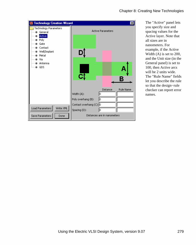
The "Active" panel letsyou specify size andspacing values for theActive layer. Note thatall sizes are innanometers. Forexample, if the ActiveWidth (A) is set to 200,and the Unit size (in theGeneral panel) is set to100, then Active arcswill be 2 units wide.The "Rule Name" fieldslet you describe the ruleso that the design−rulechecker can report errornames.
Chapter 8: Creating New Technologies
Using the Electric VLSI Design System, version 9.07 279

The "Poly" panellets you specifysize and spacingvalues for thePolysilicon layer.The "Rule Name"fields let youdescribe the rule sothat the design−rulechecker can reporterror names.
The "Gate" panel letsyou specify size andspacing values for thePolysilicon layer intransistors. The "RuleName" fields let youdescribe the rule so thatthe design−rule checkercan report error names.
Chapter 8: Creating New Technologies
280 Using the Electric VLSI Design System, version 9.07

The "Contact" panellets you specify sizeand spacing values forthe Contact layer. The"Rule Name" fieldslet you describe therule so that thedesign−rule checkercan report errornames. Note that"inline" spacing is forone−dimensionalarrays of contacts and"array" spacing is fortwo−dimensionalarrays.
Chapter 8: Creating New Technologies
Using the Electric VLSI Design System, version 9.07 281

The "Well/Implant"panel lets you specifysize and spacing valuesfor the Well andImplant layers. The"Rule Name" fields letyou describe the rule sothat the design−rulechecker can reporterror names.
Chapter 8: Creating New Technologies
282 Using the Electric VLSI Design System, version 9.07
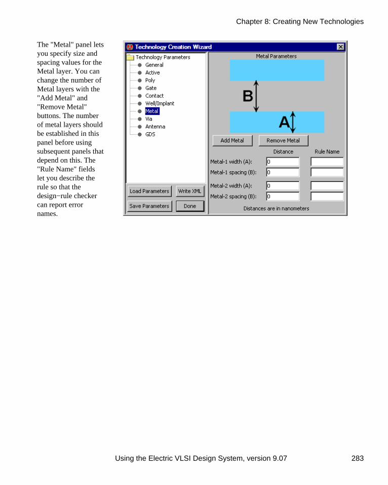
The "Metal" panel letsyou specify size andspacing values for theMetal layer. You canchange the number ofMetal layers with the"Add Metal" and"Remove Metal"buttons. The numberof metal layers shouldbe established in thispanel before usingsubsequent panels thatdepend on this. The"Rule Name" fieldslet you describe therule so that thedesign−rule checkercan report errornames.
Chapter 8: Creating New Technologies
Using the Electric VLSI Design System, version 9.07 283

The "Via" panel letsyou specify size andspacing values for theVia layer. A popup letsyou select the desiredvia. Note that the"Metal" panel should becompleted beforefilling−in this panel sothat the proper numberof via layers is shown.The "Rule Name" fieldslet you describe the ruleso that the design−rulechecker can report errornames.
Chapter 8: Creating New Technologies
284 Using the Electric VLSI Design System, version 9.07

The "Antenna" panel lets youspecify antenna ratios for alllayers. Note that the "Metal"panel should be completed beforefilling−in this panel so that theproper number of metal layers isshown. The values here are themaximum ratio of polysiliconand metal layers to the area ofconnected transistors. Forexample, if the Metal−1 ratio is200, then it is an error to haveMetal−1 connected to transistorsif the area of the Metal−1 is morethan 200 times the area of thetransistors. See Section9−3−2 for more on antenna ratiochecking.
The "GDS" panel letsyou specify GDS layernumbers for all layers.Note that the "Metal"panel should becompleted beforefilling−in this panel sothat the proper numberof metal layers isshown.
Importing Data from a Text File
This section details features not covered by the Technology Creation Wizard GUI. These features are definedin the same text file used to backup the panel values. Once they are uploaded into Electric with the "LoadParameters" button, the new features will be included in the XML file describing the technology (afterpressing the "Write XML" button). You can edit the Parameters file and add these commands:
@extra_layer allows you to add non−standard layers to a given technology. New layers have aname, and a list of attributes, separated by ":"
1.
Chapter 8: Creating New Technologies
Using the Electric VLSI Design System, version 9.07 285

Format: @extra_layer = (<layer name>, attribA=<valueA>:attribB=<valueB>)
The possible attributes are:
G: GDS number♦ C: Layer color and pattern♦ F: Layer function♦ W: Layer width♦ S: Layer spacing rule♦ M: Layer min. width rule♦ A: Enables layer arc♦ T: Layer thickness♦ H: Layer height for 3D view♦
Example: @extra_layer = (LayerA,
G=1:C=[0.0.255.{32896/16448/8224/4112/2056/1028/514/257/32896/16448/8224/4112/2056/1028/514/257}]:F=METAL2:W=1:A:S={2/"LayerARule1"}:M={3/"LayerA Rule2"}:T=4:H=1);
@metal_contacts_series is an alternative method to define the typical metal contacts. In this case,the two metal contact sizes are defined and the system will include the corresponding via. Since DRCrules are identical for a group of metals, a set of metal pairs can be specified for the same rules. Thismethod allows to defined crossed contacts or zero−enclosure contacts.
2.
Format: @metal_contacts_series = [(metalALayerValueX, "metalALayerRuleX",
metalALayerValueY, "metalALayerRuleY")(metalBLayerValueX, "metalBLayerRuleX",metalBLayerValueY, "metalBLayerRuleY")][{metalA#,metalB#}...{,}];
Example: @metal_contacts_series = [(30, "VIAx.EN.2", 30, "VIAx.EN.2")(30,
"VIAx.EN.2", 30, "VIAx.EN.2")][{1,2}{3,2}{3,4}{5,4}];
@nomulti_contacts_series defines contacts that do not add extra cuts when large; they always havejust one cut, centered in the middle. There is no limit in the number of layers however the last layeris considered the cut of the contact.
3.
Format: @nomulti_contacts_series = [(firstLayerValueX, "firstLayerRuleX",
firstLayerValueY, "firstLayerRuleY")...(nLayerValueX, "nLayerRuleX",nLayerValueY, "nLayerRuleY")][{firstLayerName,...,nLayerName}];
Example: @nomulti_contacts_series = [(−40000, "ZeroSize", −40000,
"ZeroSize")(5000, "Given.Ext", 5000, "Given.Ext")(40000, "Given.CutSize", 40000,"Given.CutSize")][{Metal−1,RDL,AL_PAD}];
Chapter 8: Creating New Technologies
286 Using the Electric VLSI Design System, version 9.07

Chapter 9: Tools
9−1: Introduction To Tools
There are many different tools available in Electric for doing both synthesis and analysis of circuitry.Synthesis tools include routers, compactors, circuit generators, and so on. Analysis tools include design−rulecheckers, network comparison, and many simulators. To see a list of tools, including which ones are active,use the List Tools command (in menu Tools). This chapter covers many of the tools available in Electric.
When a tool is running, it may take a long time. You can see it under the "JOBS" entry of the cell explorer(see Section 4−5−2). After a tool has run, it may report errors in the ERRORS section of the cell explorer. Tobrowse these errors, use the Show Next Error and Show Previous Error commands (in menu Edit /Selection) or type the ">" and "<" keys. To force an error to be shown in the current window instead ofpopping−up a new window for each cell, use Show Next Error, same Window and Show Previous Error,same Window (the "[" and "]" keys). There are also display preferences to control error display (in menuFile / Preferences..., "Display" section, "Display Control" tab, see Section 4−3): "Show cell results in newwindow" forces errors to display in a different window for each different cell; "Shift window to show errors"pans and zooms the window to focus on each new error. If an error involves multiple objects, use ShowSingle Geometry (the "/" key) to cycle through them individually. Use Show Current Collection ofErrors to highlight all errors.
A number of common tool controls are available in the General Preferences (in menu File / Preferences...,"General" section, "General" tab), especially in the "I/O" and "Jobs" section.
The I/O section lets you control the reading and writing of files. Most of the commands to generate an inputdeck for a simulator (a netlist) prompt the user for the desired file. If "Show file−selection dialog beforewriting netlists" is unchecked, however, the file is written (or overwritten) without prompt. This is useful inrepetitive iterations of design/simulate, and saves the cumbersome file−selection dialog. However, it can bedangerous because it overwrites files without asking.
When reading and writing files, Electric remembers the last directory and uses it in subsequent file selectiondialogs. Since different types of files are often stored in different locations, the system remembers manydifferent directories, organized by type. Thus, there may be a current directory for "Database" work (libraryfiles), for Spice simulation, etc. Choose the type of file to examine and change the directory associated withit.
In the "Jobs" section, "Beep after long jobs" requests that any job which runs longer than a minute make abeep sound when done. The "Verbose mode" requests that all changes made by a job be described in themessages window.
You can set the maximum number of errors that will be reported at once. By default, there is no limit to thenumber of errors.
Using the Electric VLSI Design System, version 9.07 287

For more information about "Maximum undo history", see Section 6−7.
The "Logging Options" section controls Electric log files. By default, log files are placed in the system'stemporary directory (java.io.tmpdir), but this can be disabled by unchecking "Enable logging." Bydefault, only one log file is created which is overwritten in subsequent Electric sessions. Checking "Multiplelogs" causes each log file to have a unique name so that multiple files are saved.
For more information about the "Memory" section, see Section 1−3.
The "Database"section controlsaspects of the Electricdatabase that do notaffect most users.Electric can run astwo processes: a clientthat manages thedisplay and a serverthat manages thedatabase. By checking"Use Client / Serverinteractions", Electricwill use thisexperimentalconfiguration.Checking "SnapshotLogging" requestsdebugginginformation on theclient/serverinteractions.
Chapter 9: Tools
288 Using the Electric VLSI Design System, version 9.07

9−2: Design Rule Checking (DRC)
9−2−1: Introduction to DRC
There are three built−in design−rule checkers: incremental, hierarchical, and schematic. After analysis of thecircuit, you can review the errors by typing ">" and "<" to step to the next and previous error that was found.You can also see a list of errors in the cell explorer (see Section 4−5−2).
Incremental DRC
The incremental design−rule checker is always running, examining your layout, and issuing error messageswhen an error is detected. It checks only the current cell, and does not consider the contents of cell instances,lower in the hierarchy. It therefore offers an instant analysis, but not a complete one.
The incremental DRC also shows simple design−rules violations when a node or arc is being moved. SeeSection 2−4−1 for more on this.
Hierarchical DRC
The hierarchical design−rule checker uses the same rules and techniques as the incremental checker, but itchecks all levels of hierarchy below the current cell. To run it, use the Check Hierarchically command (inmenu Tools / DRC). To check only a selected subset of the current cell, use Check SelectionHierarchically.
When checking hierarchically, it may be the case that a cell is not designed to be checked in isolation, butmust have higher levels of the hierarchy considered. For example, notches in the well areas may be coveredat higher levels of hierarchy. When this happens, tell the DRC to ignore the cell by using the command AddSkip Annotation to Cell.
Chapter 9: Tools
Using the Electric VLSI Design System, version 9.07 289

Schematic DRC
The schematic design−rule checker looks for issues that make drawing or editing of the cell difficult. Theseare the errors that is finds:
Nodes: Nodes whose parameters don't match the cell definition (check export names, units, andvisibility).
♦
"Stranded" pins: with no connections, exports, or attached text.♦ "Inline" pins: those that sit in a line between two arcs (both of which could be replaced by asingle straight arc).
♦
Nodes whose ports touch but are not connected.♦ Invisible pins with text that is offset from the node center (this is an internal consistencycheck).
♦
Nodes whose names are the same as network names in the cell.♦ Schematic exports whose characteristics are different from the equivalent export in the icon.♦
1.
Arcs: Unnamed arcs that "dangle": one end is unconnected and unexported (does not apply tobusses).
♦
Arcs that end on another arc without connecting to them.♦ Bus arcs whose width is inconsistent with its two nodes.♦ Bus pins that "float": do not connect to bus arcs and are not exported.♦ Bus taps that connect to a wire which is not part of the bus.♦ Bus pins that connect to more than 1 wire.♦ Network names that differ only by their case (i.e. networks "A" and "a" are actually differentnetworks).
♦
2.
Chapter 9: Tools
290 Using the Electric VLSI Design System, version 9.07

9−2−2: DRC Preferences
To control the DRC,use the DRCPreferences (in menuFile / Preferences...,"Tools" section,"DRC" tab).
By default, theincrementaldesign−rule checkeris on. To turn it off,uncheck the "On"checkbox in the"Incremental DRC"section. You can alsocontrol theincremental displayof design−ruleviolations that occurswhen moving nodesand arcs (see Section2−4−1).
There are three levels of checking that can be requested for the Hierarchical DRC. Each level of checkingconsumes more time and finds more errors.
"Report just 1 error per cell" tells the system to stop checking a cell after the first error has beenfound. By using this option, you can more quickly determine which cells in the design are correct,without knowing exactly where the errors lie. Then, you can go to the cells with errors and do a morecomplete check.
•
"Report just 1 error per pair of geometries" is the default. The algorithm works by checking designrules per each possible pair of geometries and it stops when the first violation for a given pair isfound in this mode.
•
"Report all errors" tells the system to continue checking all possible violations in a pair ofgeometries, even if an error has already been found. This is the exhaustive mode and therefore time
•
Chapter 9: Tools
Using the Electric VLSI Design System, version 9.07 291

consuming that will report all violations found.
Hierarchical errors appear in the cell explorer (see Section 4−5−2). Since there can be many errors involvingmany different rules, you can control how they appear by setting "Report Errors" to:
"By Cell" creates a separate error section for each cell. This is the default.• "By Rule" creates a separate error section for each different design rule.• "Flat" creates a single error section with all errors.•
Users with multiprocessor computers can check "Multi−threaded DRC" to speed−up the hierarchicaldesign−rule checking process.
The design−rule checker remembers the date of the last clean check. If a cell has not changed since then, itdoes not need to be rechecked. This date information can be stored in the libraries (requiring them to besaved) or can be held only in Electric's memory (requiring them to be rechecked if Electric is restarted). Youcan also request that all date information be removed so that a full recheck is done. To see which cells havepassed DRC, use the General Cell Lists... command (in menu Cell / Cell Info) A "D" is shown in on theright for cells that are DRC current (see Section 3−7−1).
MOS contact nodes automatically increase the number of cuts when they grow larger (see Section 7−4−1).Because of this, very large contact nodes can create excessive work for the design−rule checker as itexamines each of the cuts. To save time, check the "Ignore center cuts in large contacts" check box, whichwill examine only the cut layers around the edges of contact nodes.
DRC rules for new technologies might require special rules, which can be time consuming. To ignore theseerrors, check "Ignore area checking" (for minimum area rules) and "Ignore extension rules" (for specialoverlap rules).
After DRC is complete, errors are available in the the cell explorer. If you wish to see errors while DRC isrunning, check "Interactive logging", and the errors will appear incrementally.
The final DRC control is how minimum area detection is done. Setting "MinArea Algorithm" to "Simple"uses an algorithm that is slower. Setting "MinArea Algorithm" to "Local" uses an algorithm that is faster butconsumes more memory.
Chapter 9: Tools
292 Using the Electric VLSI Design System, version 9.07

9−2−3: Design Rules
Four types of errors are detected by the incremental and hierarchical design−rule checkers. Spacing errors arecaused by geometry that is too close, but not connected. Notch errors are caused by geometry that is tooclose, but connected. Minimum size errors are caused by geometry that is too small. Resolution errors arecaused by geometries that are smaller than a specified limit.
In addition to examining geometry, the design−rule checkers use connectivity information to help findviolations. This use of network information helps the designer to debug circuit connectivity. For example, iftwo overlapping nodes are not joined by an arc, they may be considered to be in violation, even if theirgeometry looks right. This is because the checkers know what is connected and have a separate set of rulesfor such situations.
To help guide the design−rule checker, an "exclusion" layer can be placed over areas that are not to beexamined. This exclusion layer is created by clicking the "Misc." entry of the component menu and selecting"DRC Exclusion" (see Section 7−6−3). Any errors that fall inside of this node's area are ignored.
To edit the design rules, use the Design Rules Preferences (in menu File / Preferences..., "Technology"section, ""Design Rules" tab). The dialog allows you to examine and modify the spacing limits for the currenttechnology. Each rule has a numeric value (size or distance) as well as a textual description of the rule. Thedialog is divided into two parts: "Node Rules" and "Layer Rules".
In the "Node Rules" section, you may set the minimum size of each node in the current technology.
In the "Layer Rules" section, you may set the minimum size, area, and enclosure area of each layer. You mayalso set the inter−layer spacing (between the "From Layer" and the "To Layer"). Use the "Show only 'to'entries with rules" to restrict the displayed rules to those with valid values.
The layer−to−layer spacing rules appear in 3 forms: normal, wide, and multicut. Normal rules come in threeflavors: connected, unconnected, and edge. The connected rules apply to pieces of geometry that areelectrically connected; the unconnected rules apply to unconnected geometry; edge rules apply tounconnected layers and ignore overlap when considering spacing distance.
The wide rules apply to large geometry. Although some technologies may have many different rules fordifferent definitions of "large", the MOSIS CMOS technology has only one such rule. Additional rules can becontrolled with the "Add Wide Rule" and "Delete Wide Rule" buttons.
The bottom of the dialog has a "Min resolution" field, which is the minimum resolution that can bemanufactured.
Chapter 9: Tools
Using the Electric VLSI Design System, version 9.07 293

If zero, no resolutioncheck is done. Whenchecking resolution,all geometry of thatsize or less will beflagged as resolutionerrors. For example,current MOSIS rulesrequire that noboundaries bequarter−unit or less,so a value of .25 inthis field will detectsuch violations.
When rules havebeen changed, theyare saved with yourPreferences. To savethem independentlyof the Preferences,use the Export DRCDeck... command (inmenu Tools / DRC)to write an XML filewith the design rules.Use the Import DRCDeck... command torestore these rules.
Note that the MOSIS CMOS design rule 6.7b is not checked by Electric because it is difficult to detectproperly. This error is never fatal, and the worst case of missing this error is that active and poly are closer by1/2 grid unit, which merely results in an increase in capacitive coupling between them. If this fringingcapacitance is important, you've probably got so much polysilicon in your circuit that it has bigger problems.
9−2−4: Coverage Rules
Some foundries request that each layer occupy a minimum percentage of the chip. To enforce such rules,additional pieces of geometry must be placed around the chip to fill that layer.
Chapter 9: Tools
294 Using the Electric VLSI Design System, version 9.07
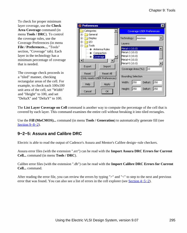
To check for proper minimumlayer coverage, use the CheckArea Coverage command (inmenu Tools / DRC). To controlthe coverage rules, use theCoverage Preferences (in menuFile / Preferences..., "Tools"section, "Coverage" tab). Eachlayer in the technology has aminimum percentage of coveragethat is needed.
The coverage check proceeds ina "tiled" manner, checkingrectangular areas of the cell. Forexample, to check each 100x100unit area of the cell, set "Width"and "Height" to 100, and set"DeltaX" and "DeltaY" to 100.
The List Layer Coverage on Cell command is another way to compute the percentage of the cell that iscovered by each layer. This command examines the entire cell without breaking it into tiled rectangles.
Use the Fill (MoCMOS)... command (in menu Tools / Generation) to automatically generate fill (seeSection 9−8−2).
9−2−5: Assura and Calibre DRC
Electric is able to read the output of Cadence's Assura and Mentor's Calibre design−rule checkers.
Assura error files (with the extension ".err") can be read with the Import Assura DRC Errors for CurrentCell... command (in menu Tools / DRC).
Calibre error files (with the extension ".db") can be read with the Import Calibre DRC Errors for CurrentCell... command.
After reading the error file, you can review the errors by typing ">" and "<" to step to the next and previouserror that was found. You can also see a list of errors in the cell explorer (see Section 4−5−2).
Chapter 9: Tools
Using the Electric VLSI Design System, version 9.07 295

9−3: Electrical Rule Checking (ERC)
9−3−1: Well and Substrate Checking
To check the well and substrate layers, use the Check Wells command (in menu Tools / ERC). This does amore thorough job of checking the layers than the design−rule checker.
After analysis is done, you can review the errors by typing ">" to see the next error and "<" to see theprevious error. You can also see the list of errors in the cell explorer (see Section 4−5−2).
You can control the Well Checker with the Well Check Preferences (in menu File / Preferences..., "Tools"section, "Well Check" tab).
The Well Checker makes sure that there are well contacts in every area of well. The dialog allows you checkfor just 1 well contact in each cell, or not to check for contacts at all.
Chapter 9: Tools
296 Using the Electric VLSI Design System, version 9.07

The Well Checker also checks that there is a connection to power and ground in the appropriate places. Youcan disable these checks in the "Well Check" dialog.
An additional well check is to find the farthest distance from a substrate contact to the edge of that area. Thischeck takes more time to do, and so it can be disabled.
The Well Checker can check spacing rules between well areas. Although this is generally the domain of theDesign Rule Checker (DRC), it can be requested here by checking "Check DRC Spacing Rules for Wells".Since the well checker has not been designed for DRC purposes, the algorithm is not efficient and thereforethe option is off by default.
Finally, the Well Checker is able to use multiple processors to speed up its task. This can be disabled, or thenumber of processors can be reduced with the "Use multiple processors" checkbox and field.
9−3−2: Antenna Rule Checking
Antenna rules are required by some IC manufacturers to ensure that the transistors of the chip are notdestroyed during fabrication. In such processes, the wafer is bombarded with ions in order to create thepolysilicon and metal layers. These ions must find a path through the wafer (to the substrate and active layersat the bottom). If there is a large area of poly or metal, and if it connects ONLY to gates of transistors (not tosource or drain or any other active material) then these ions will travel through the transistors. If the ratio ofthe poly or metal layers to the area of the transistors is too large, the transistors will be destroyed.
To check for antenna rule violations, use the Antenna Check command (in menu Tools / ERC). Afteranalysis is done, you can review the errors by typing ">" to see the next error and "<" to see the previouserror. You can also see the list of errors in the cell explorer (see Section 4−5−2).
You can control the AntennaChecker with the AntennaRules Preferences (in menuFile / Preferences..., "Tools"section, "Antenna Rules"tab). The dialog lets youmodify the required ratio of alayer (poly or metal) to thetransistor area.
Chapter 9: Tools
Using the Electric VLSI Design System, version 9.07 297

9−4: Simulation Interface
9−4−1: Introduction to Simulation
Electric has two built−in simulators: IRSIM (see Section 9−5−1) and ALS (see Section 9−5−2). It also cangenerate decks for many other simulators. The ability to interface to external simulators is controlled with theTools / Simulation (Spice), Tool / Simulation (Verilog), and Tools / Simulation (Others) menus.
Be aware that the Electric distribution does not come packaged with these external simulators. You must getyour own copy of Spice, Verilog, or any other simulator mentioned here.
Electric can write netlists for these simulators:
Simulator Level Netlist Command
CDL circuit Tools / Simulation (Spice) / Write CDL Deck...
COSMOS switch Tools / Simulation (Others) / Write COSMOS Deck...
ESIM/RNL switch Tools / Simulation (Others) / Write ESIM/RNL Deck...
FastHenry inductance Tools / Simulation (Others) / Write FastHenry Deck...
IRSIM switch Tools / Simulation (Others) / Write IRSIM Deck...
Maxwell circuit Tools / Simulation (Others) / Write Maxwell Deck...
MOSSIM switch Tools / Simulation (Others) / Write MOSSIM Deck...
PAL gate Tools / Simulation (Others) / Write PAL Deck...
RSIM switch Tools / Simulation (Others) / Write RSIM Deck...
SILOS functional Tools / Simulation (Others) / Write SILOS Deck...
Spice circuit Tools / Simulation (Spice) / Write Spice Deck...
Tegas functional Tools / Simulation (Others) / Write Tegas Deck...
Verilog functional Tools / Simulation (Verilog) / Write Verilog Deck...
For more control of netlist generation, see Section 3−9−3.
For more information on Spice, see Section 9−4−3; for Verilog, see Section 9−4−2; and for FastHenry, seeSection 9−4−5.
Chapter 9: Tools
298 Using the Electric VLSI Design System, version 9.07

9−4−2: Verilog
Electric can produce input decks for Verilog simulation with Write Verilog Deck... command (in menuTools / Simulation (Verilog)). For VerilogA format, use the Write VerilogA Deck... command. After thishas been done, you must run Verilog externally to produce a ".dump" file. Note that the Electric distributiondoes not come with a Verilog simulator: you must obtain it separately.
After running a Verilog simulation, you can read the ".dump" file into Electric and display it in a waveformwindow. This is done with the Plot Simulation Output, Choose File... command (in menu Tools /Simulation (Verilog)). You can also use the Plot Simulation Output, Guess File command if the cell nameand file name are the same. The Verilog simulation information is then shown in a digital waveform window(see Section 4−11 for more). Electric also understands the output of Modelsim and can plot it.
Before generating Verilog decks, it is possible to annotate circuits with additional Verilog text that will beincluded in the deck. To add Verilog code to this cell, select "Verilog Code" under the "Misc." entry in thecomponent menu of the side bar. To add a Verilog declaration in this cell, select "Verilog Declaration" underthe "Misc." entry in the component menu. To add a Verilog parameter to this cell, select "Verilog Parameter"under the "Misc." entry in the component menu. To add external Verilog code, outside of this cell, select"Verilog External Code" under the "Misc." entry in the component menu. These pieces of text can bemanipulated like any other text object (see Section 6−8−1 on text). For an example of Verilog layout andcode, look at the cell "tool−SimulateVERILOG" in the Samples library (get this library with the LoadSample Cells Library command, in menu Help).
Additional control of Verilog deck generation is accomplished with the Verilog Preferences (in menu File /Preferences..., "Tools" section, "Verilog" tab).
Chapter 9: Tools
Using the Electric VLSI Design System, version 9.07 299

The left side is the Verilog Project Preferences which has two controls:
"Use ASSIGN Construct" lets you choose whether or not to use the Verilog "assign" construct.• "Default wire is Trireg" lets you control the type of Verilog declaration that will be used for wires("wire" by default, "trireg" if checked). Note that this can be overridden with the Set VerilogWire command (in menu Tools / Simulation (Verilog)).
•
Another property that can be assigned to transistors is their strength. The Weak command (in menu Tools /Simulation (Verilog) / Transistor Strength) sets the transistor to be weak. The Normal command restoresthe transistor to be normal strength.
Still more control of Verilog deck generation is accomplished with the Verilog User Preferences in the rightside of the dialog.
"Run Placement after import" requests that the Placement tool be used to organize components afterreading Verilog (see Section 9−13 for more on Placement).
•
"Make Layout Cells (not Schematics)" requests that conversion from Verilog to circuitry producelayout instead of schematics. The difference is that layout has unrouted arcs for connectivity andbreaks busses into their individual components.
•
"Do not netlist Standard Cells" writes a netlist that excludes Standard Cells. Any cell marked as aStandard Cell will be netlisted only as instances, but no module definition will be written. Thisallows Standard Cell based simulation or Static Timing Analysis to be performed on the netlist. SeeSection 3−7−3 for more on marking cells as "standard cells".
•
"Netlist Non−Standard Cells" allows you to write Standard Cell Verilog netlists that includenon−Standard Cells.
•
"Preserve Verilog formatting" keeps the indentation and other formatting of all inserted text.• "Parameterize Verilog module names" causes Verilog deck generation to create multiple Verilog celldescriptions when the cells are parameterized.
•
"Write Separate Module for each Icon" requests that schematic cells with multiple icons be writtenmultiple times to the Verilog deck, once for each icon variation. This preserves the hierarchicalstructure of the circuit, but creates duplicate modules.
•
"Do not include empty modules" requests that empty cells be dropped from the Verilog output.•
Chapter 9: Tools
300 Using the Electric VLSI Design System, version 9.07

A final set of Verilog controls can be found in the Verilog Model Files Preferences (in menu File /Preferences..., "Tools" section, "Verilog Model Files" tab). The Verilog Model Files Preferences dialog letsyou control how each cell is represented in the Verilog.
The default is to construct the Verilog from the actual cell contents. If there is an equivalent layout cell, it canbe used (instead of the schematic). You can also choose to use the "Verilog" view, which contains Verilogtext for that cell. Finally, you can request that an external model file be used. These choices allow you tocreate your own definitions in situations where the derived Verilog would be too complex or otherwiseincorrect.
Chapter 9: Tools
Using the Electric VLSI Design System, version 9.07 301
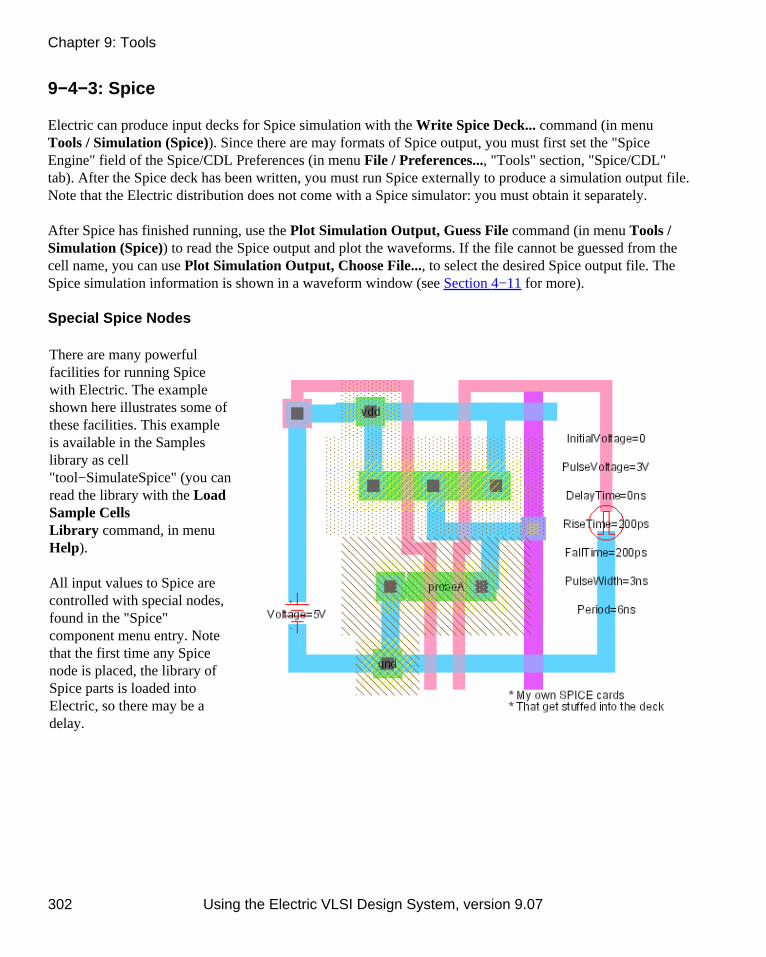
9−4−3: Spice
Electric can produce input decks for Spice simulation with the Write Spice Deck... command (in menuTools / Simulation (Spice)). Since there are may formats of Spice output, you must first set the "SpiceEngine" field of the Spice/CDL Preferences (in menu File / Preferences..., "Tools" section, "Spice/CDL"tab). After the Spice deck has been written, you must run Spice externally to produce a simulation output file.Note that the Electric distribution does not come with a Spice simulator: you must obtain it separately.
After Spice has finished running, use the Plot Simulation Output, Guess File command (in menu Tools /Simulation (Spice)) to read the Spice output and plot the waveforms. If the file cannot be guessed from thecell name, you can use Plot Simulation Output, Choose File..., to select the desired Spice output file. TheSpice simulation information is shown in a waveform window (see Section 4−11 for more).
Special Spice Nodes
There are many powerfulfacilities for running Spicewith Electric. The exampleshown here illustrates some ofthese facilities. This exampleis available in the Sampleslibrary as cell"tool−SimulateSpice" (you canread the library with the LoadSample CellsLibrary command, in menuHelp).
All input values to Spice arecontrolled with special nodes,found in the "Spice"component menu entry. Notethat the first time any Spicenode is placed, the library ofSpice parts is loaded intoElectric, so there may be adelay.
Chapter 9: Tools
302 Using the Electric VLSI Design System, version 9.07

The Spice nodes described here are Electric's default set. However, additional sets can (and have) beenwritten. To choose another set, use the Spice/CDL Preferences (in menu File / Preferences..., "Tools"section, "Spice/CDL" tab). Under the setting "Spice primitive set", choose another set. A second set of nodes,called "SpicePartsS3", is tailored towards special Spice3.
In this example, there is a 5−volt supply on theleft. It was created by using the "DC Voltage"entry under "Spice" entry of the componentmenu. Once placed, the text that reads"Voltage=0V" can be selected and modified(either with Object Properties... or bydouble−clicking on it). The Pulse input signal onthe right is created with the "Pulse" entry under"Spice" (it has 7 parameters).
There are both voltage and current sources, inAC and DC form. There is a piecewise−linear(PWL) source, and two pulses (voltage andcurrent). A set of "two−gate" devices are alsoavailable: "CCCS", "CCVS", "VCCS", "VCVS",and "Transmission".
It is possible to specify Transient, DC, or ACanalysis by using the "Transient Analysis", "DCAnalysis", and "AC Analysis" subcommands.The "Probe" lets you graphically specify signalsof interest to Spice. Only one such element mayexist in a circuit.
For advanced users, there are two special Spice nodes: "Node Set" and "Extension". The Node Set may beparameterized with an arbitrary piece of Spice code. Truly advanced users may create their own Spice nodesby modifying the cells in the Spice library (see next Section).
Chapter 9: Tools
Using the Electric VLSI Design System, version 9.07 303

Spice Text
This example also shows the ability to add arbitrary text to the Spice deck, as shown in the lower−right. Tocreate this text, use the "Spice Code" or "Spice Declaration" entries under the "Misc." button in thecomponent menu. These command create text that can be modified arbitrarily. Whatever the text says will beadded to the Spice deck (declarations go near the top).
Another option that can be used when modeling transistors and other component is to set a specific Spicemodel to use for that component. To set a node's model, select it and use the Set Spice Model... command (inmenu Tools / Simulation (Spice)).
The Add Multiplier subcommand places a multiplier on the currently selected node. Multipliers (also called"M" factors) scale the size of transistors inside of them.
Another piece of text that can be added to a circuit is for separate flattened analysis files. This is useful forNanosim timing assertions, hierarchical measurements, etc. The Add Flat Code subcommand places a pieceof text in the circuit that will be flattened and written to a separate file with the "flatcode" extension.Flattening adds global scope to these statements. For example, if you place a Nanosim timing assertion in acell with the flat code
tv_node_setuphold $(clk) rf $(in) rf 100p 100p
and there are 3 instances of the cell, then there will be 3 flattened assertions in the flatcode file:tv_node_setuphold xtop.xflop1.clk rf xtop.flop1.in rf 100p 100p
tv_node_setuphold xtop.xflop2.clk rf xtop.flop2.in rf 100p 100p
tv_node_setuphold xtop.xflop3.clk rf xtop.flop3.in rf 100p 100pIf clk is actually a single signal that comes from the top level, it is smart enough to recognize this:
tv_node_setuphold clk rf xtop.flop1.in rf 100p 100p
tv_node_setuphold clk rf xtop.flop2.in rf 100p 100p
tv_node_setuphold clk rf xtop.flop3.in rf 100p 100p
Chapter 9: Tools
304 Using the Electric VLSI Design System, version 9.07

Spice/CDL Preferences
Some nongraphical information can also be given to the Spice simulator with the Spice/CDL Preferences (inmenu File / Preferences..., "Tools" section, "Spice/CDL" tab).
Chapter 9: Tools
Using the Electric VLSI Design System, version 9.07 305

The top part of this dialog allows you to control Spice deck generation:
Spice engine Can be Spice 2, Spice 3, HSpice, PSpice, Gnucap, SmartSpice, Spice Opus, Xyce,HSpice for Assura, or HSpice for Calibre.
•
Spice level Can be 1, 2, or 3 (not used anymore).• Resistor shorting Specifies which resistors get shorted when writing a Spice netlist from aschematic. Choices are:
"none" no resistors are shorted. This preserves all resistors (useful for simulations).♦ "normal only" only normal schematic resistors are shorted. This is useful when runningexternal LVS tools like Calibre and Assura against a Spice netlist because it shorts outparasitic resistors (such as from wire models) but preserves poly resistors which are actualdevices in the layout.
♦
"normal and poly" both normal and poly schematic resistors are shorted. This is availableonly because the Verilog netlister uses the same netlisting subsystem; it is unlikely that youwill want this setting for Spice netlisting.
♦
•
Parasitics Controls the writing of parasitics in the Spice deck. Choices are: "Trans area/perim only" which writes the area and perimeter of transistor active but does notwrite any Resistor/Capacitor information.
♦
"Conservative RC" writes Resistor/Capacitor information (in addition to the area/perimeter).♦
•
Globals Has three options for the treatment of global signals (such as power and ground): "No special treatment" causes globals to be treated like other signals.♦ "Use .GLOBAL block" places global signals in a .GLOBAL block (not supported by allversions of Spice).
♦
"Create .SUBCKT ports" causes globals to be added to .SUBCKT headers as explicit ports.Note that this preference should be used when Global Partitions are in use (see Section6−9−5).
♦
•
Spice primitive set Switches between Spice primitive sets. Currently there are only two: "spiceparts"and "spicepartsG3".
•
Max chars per line: Sets the maximum number of characters that will be written on a single line ofSPICE output. Lines longer than this will be split into multiple lines.
•
Write VDD/GND in top cell Whether to write power and ground signals in the top−level cell.• Use cell parameters When set, any parameters defined on a cell will be turned into a Spiceparameter (this assumes that your Spice engine can handle parameters). When not checked, eachparameterized cell appears multiple times in the deck, once for each different parameter combination.See Section 6−8−5 for more on parameters.
•
Write trans sizes in units Requests that the Spice deck contain scalable size information instead ofabsolute size information.
•
Write .subckt for top cell Requests that a the top−level cell be written as a subcircuit, and a callmade to it. The default is to write the top−level cell without a subcircuit wrapper.
•
Write .end statement Requests that an .end statement be written at the end of the deck. This can bedisabled in situations where the deck is part of a larger Spice deck.
•
Write empty subcircuits Requests that all subcircuits be written to the deck, even those withnothing in them.
•
Use Header cards from files with extension specifies that header cards (placed at the start of theSpice deck) can be found in a file with the cell's name and the given extension.
•
Chapter 9: Tools
306 Using the Electric VLSI Design System, version 9.07

Use Header cards from file lets you specify the file with header cards.• No Header cards prevents any header cards from being written to the Spice deck.• Use Trailer cards from files with extension specifies that trailer cards (placed at the end of theSpice deck) can be found in a file with the cell's name and the given extension.
•
Use Trailer cards from file lets you specify the file with trailer cards.• No Trailer cards prevents any trailer cards from being written to the Spice deck.•
Note that the header and trailer information is specific to a particular technology. If you set this informationfor one technology, but then use another technology when generating the Spice deck, the information thatyou set will not be used. Note also that schematics, although a technology in Electric, are not considered tobe Spice technology. You can set the proper layout technology that you want to use when dealing withschematics by using the "Layout technology to use for schematics" popup. This popup can be found in theTechnology Preferences (in menu File / Preferences..., "Technology" tab, see Section 7−1−2).
The middle part of the dialog controls how Spice can be run after a deck has been written:
After writing deck Electric can create an external process as specified by the user to run Spice onthe generated netlist. If the pull−down box is set to "Don't Run", nothing is done. If the pull−downbox is set to "Run, Ignore Output", the external process is run, and the user is notified when it isfinished. If set to "Run, Report Output", a dialog box is opened to show the user the output producedby the process. Please note that this is a process, and not a command line command. For example,echo blah > file will NOT work. Encapsulate it in a script if you want to do such things.
•
Run program Identifies the Spice program to run.• With args the arguments passed to the program.• Use dir if specified, this is the working directory of the program.• Overwrite existing file (no prompts) this will overwrite the existing netlist without prompting theuser.
•
Run probe this will run the waveform viewer on the output of the Spice run.• Help tells which environment variables are exported to be used by the process.•
The following variables are available to use in the program name and arguments:
${WORKING_DIR} The current working directory.• ${USE_DIR} The Use Dir field, if specified (otherwise defaults to WORKING_DIR).• ${FILENAME} The output file name (with extension).• ${FILENAME_NO_EXT} The output file name (without extension).• ${FILEPATH} The full path to the output file.•
The bottom part of the dialog has two controls:
How Spice decks are handled after being read into Electric. The only option is whether the placementtools should be run on the circuits to make them look cleaner.
•
How CDL decks are handled. The only option is whether or not to include slashes in instance names(some CDL implementations need this).
•
Chapter 9: Tools
Using the Electric VLSI Design System, version 9.07 307

Another set of controls can be used is the Spice Model Files Preferences (in menu File / Preferences...,"Tools" section, "Spice Model Files" tab). This dialog allows you to control how each cell is represented inthe Spice deck.
The default is to construct the Spice from the actual cell contents. If there is an equivalent layout cell, it canbe used (instead of the schematic). You can also choose to use the "Verilog" view, which contains Verilogtext for that cell (it will be converted to Spice). Finally, you can request that an external model file be used.Note that in the case of external model files, the specified disk file is referenced by adding "include" lines inthe deck. These choices allow you to create your own definitions in situations where the derived Spice wouldbe too complex or otherwise incorrect.
Another way to change the Spice representation of a cell is to use the Set Netlist Cell From File command(in menu Tools / Simulation (Spice)). This prompts for a file which will be included in the Spice deckinstead of the actual subcircuit of the cell. The file name can be seen as a piece of text in the cell, and you canedit this text to change the desired file.
Chapter 9: Tools
308 Using the Electric VLSI Design System, version 9.07
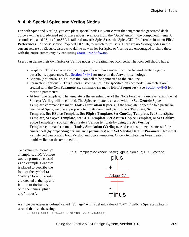
9−4−4: Special Spice and Verilog Nodes
For both Spice and Verilog, you can place special nodes in your circuit that augment the generated deck.Spice even has a predefined set of these nodes, available from the "Spice" entry in the component menu. Asecond set, called "SpicePartsS3", is tailored towards Spice3 (use the Spice/CDL Preferences in menu File /Preferences..., "Tools" section, "Spice/CDL" tab, to switch to this set). There are no Verilog nodes in thecurrent release of Electric. Users who define new nodes for Spice or Verilog are encouraged to share thesewith the entire community by contacting Static Free Software.
Users can define their own Spice or Verilog nodes by creating new icon cells. The icon cell should have:
Graphics. This is an icon cell, so it typically will have nodes from the Artwork technology todescribe its appearance. See Section 7−6−1 for more on the Artwork technology.
•
Exports (optional). This allows the icon cell to be connected to the circuitry.• Parameters (optional). This allows custom values to be specified on each node. Parameters arecreated with the Cell Parameters... command (in menu Edit / Properties). See Section 6−8−5 formore on parameters.
•
At least one template. The template is the essential part of the Node because it describes exactly whatSpice or Verilog will be emitted. The Spice template is created with the Set Generic SpiceTemplate command (in menu Tools / Simulation (Spice)). If the template is specific to a particularversion of Spice, use the appropriate template command (Set Spice 2 Template, Set Spice 3Template, Set HSpice Template, Set PSpice Template, Set GnuCap Template, Set SmartSpiceTemplate, Set Xyce Template, Set CDL Template, Set Assura HSpice Template, or Set CalibreSpice Template). You can also create a Verilog template by using the Set VerilogTemplate command (in menu Tools / Simulation (Verilog)). And can customize instances of thecurrent cell (by prepending per−instance parameters) with Set Verilog Default Parameter. Note thata single cell can contain both Verilog and Spice templates. Once a template has been created,double−click on the text to edit it.
•
To explain the format ofa template, a DC VoltageSource primitive is usedas an example. Graphicsis placed to describe thelook of the symbol (a"battery" look). Exportsare created at the top andbottom of the batterywith the names "plus"and "minus".
A single parameter is defined called "Voltage" with a default value of "0V". Finally, a Spice template iscreated that has the string:
V$(node_name) $(plus) $(minus) DC $(Voltage)
Chapter 9: Tools
Using the Electric VLSI Design System, version 9.07 309

This string contains substitution expressions of the form $(SOMETHING) where SOMETHING can be anexport, a parameter, or "node_name". In this example, $(node_name) will be replaced with the name ofthe voltage node; $(plus) will be replaced with the net name attached to the positive export;$(minus) will be replaced with the net name attached to the negative export; and $(Voltage) will bereplaced with the voltage value specified by the user.
When defining technologies, it is possible to place Spice templates onto primitive nodes (see Section 8−6).These templates can make use of two additional substitution expressions: $(width) and$(length) which access the size of the node.
9−4−5: FastHenry
FastHenry is an inductance analysis tool (see the papers of Jacob White). When a FastHenry deck isgenerated, a subset of the arcs in the current cell are written. To include an arc in the FastHenry deck, selectit and use the FastHenry Arc Properties... command (in menu Tools / Simulation (Others)).
This command presents a dialogwith FastHenry factors for theselected arc. The most importantfactor is at the top: "Include thisarc in FastHenry analysis". Bychecking this, the arc is describedin the FastHenry deck. Once thisis checked, other fields in thedialog become active. You can setthe thickness of this arc (thedefault value shown will be usedif no override is specified). Youcan set the number ofsubdivisions that will be used inheight and width (again, defaultsare shown). You can even set theheight of the two ends of the arc.
Arcs can be partitioned into different groups. Click the "New Group" button to define a group. After that,arcs can be assigned to one or more groups.
After all arcs have been marked, generate a FastHenry deck with the Write FastHenry Deck... command (inmenu Tools / Simulation (Others)). Before doing that, however, you can set other options for FastHenrydeck generation. To do this, use the FastHenry Preferences (in menu File / Preferences..., "Tools" section,"FastHenry" tab).
Chapter 9: Tools
310 Using the Electric VLSI Design System, version 9.07

This dialog allows you to set the type of frequency analysis (single frequency or a sequence specified by astart, end, and number of runs per decade). You can choose to use single or multiple−pole analysis (and ifmultiple, you can specify the number of poles). The FastHenry Preferences dialog also allows you to setdefaults for the individual arcs that will be included in the deck. You can specify the default thickness, andthe default number of subdivisions (in height and width).
Chapter 9: Tools
Using the Electric VLSI Design System, version 9.07 311

9−5: Simulation (built−in)
9−5−1: IRSIM
Electric has a built−in simulator, Stanford's IRSIM, which uses RC models to accurately simulate transistorsat a gate−level. IRSIM is not packaged with the standard Electric distribution. To obtain it, you must get theadditional "plugin" JAR file from Static Free Software (see Section 1−5 for instructions on installingplugins).
To simulate the current cell with IRSIM, use the IRSIM: Simulate Current Cell command (in menu Tools /Simulation (Built−in)). After issuing this command, a waveform window will appear to control thesimulation (see Section 4−11 for more). To generate an input deck for IRSIM without running the simulator,use the IRSIM: Write Deck... command. To simulate an IRSIM deck (that is, simulate the file, not thecircuit), use the IRSIM: Simulate Deck... command. Note: if these commands do not appear in the menu,then IRSIM has not been installed.
Since the IRSIM engine isrunning inside of Electric, youcan place stimuli on the circuitand see the results immediately(also described in Section4−11). Note that the commandto save stimuli (Save Stimuli toDisk... of menu Tools /Simulation (Built−in)) writesan IRSIM "command file"which can be edited by hand.
The Simulators Preferences (inmenu File / Preferences...,"Tools" section, "Simulators"tab), offers some controls forIRSIM. The general controls atthe top are discussed in Section4−11.
Chapter 9: Tools
312 Using the Electric VLSI Design System, version 9.07

IRSIM uses a parameter file to describe timing and parasitic information. Two of these files come packagedwith Electric ("scmos0.3.prm" and "scmos1.0.prm"), but you can create your own and tell IRSIM to use it. Inaddition to the parameter file, you can select the simulation model that IRSIM uses. The default is a RCmodel, but a Linear model is also available.
Advanced users who edit their own command files may enter specialized IRSIM debugging commands.These commands depend on a set of flags to determine the type of debugging to do. Checkboxes in the"IRSIM Debugging" section control these debugging flags.
The bottom section has two miscellaneous IRSIM controls.
"Show IRSIM commands" requests that the system display the command file instructions as they areapplied during simulation.
•
"Use Delayed X propagation" does less conservative, but potentially more accurate calculation of thetime required to propagate an undefined (X) value in the circuit. This improved propagation delaycalculation has been shown to be effective in asynchronous circuits.
•
9−5−2: ALS
Electric has a built−in gate−level simulator called ALS that can simulate schematics, IC layout, or VHDLdescriptions. The simulator already knows about MOS transistors and some digital logic gates. It can beaugmented with functional descriptions of any circuit using the hardware description language described laterin this section.
For an example of ALS simulation, load the "samples" library and simulate the cell"tool−SimulateALS{sch}". You can load the samples library with the Load Sample CellsLibrary command (in menu Help).
To begin simulation of the circuit in the current window, use the ALS: Simulate This Cell command (frommenu Tools / Simulation (Built−in)). After issuing this command, a waveform window will appear tocontrol the simulation (see Section 4−11 for more). Since the ALS engine is running inside of Electric, youcan place stimuli on the circuit and see the results immediately.
ALS is able to handle transistors with varying strength. To set a transistor to be weak, use theWeak command (in menu Tools / Simulation (Verilog) / Transistor Strength). To restore the strength tonormal, use the Normal command. Note that this must be done before simulation begins.
Preferences
The Simulators Preferences (in menu File / Preferences..., "Tools" section, "Simulators" tab) has somecontrols that affect ALS simulation. The "Multistate display" check tells the simulator to show waveformsignals with different colors to indicate different strengths. Without this, a single color is used everywhere.The other general controls at the top are discussed in Section 4−11.
Chapter 9: Tools
Using the Electric VLSI Design System, version 9.07 313

9−5−3: ALS Concepts
The user should be aware that theALS simulator translates the circuitinto VHDL, then compiles the VHDLinto a netlist for simulation. Thismeans that when a layout orschematic is simulated, two newviews of that cell are created:{VHDL} and {net.als}. Use the EditVHDL View (in menu View) to seethe VHDL code.
When simulation is requested, the cell in the current window is simulated. Date checking is performed todetermine whether VHDL translation or netlist compilation is necessary. If you are currently editing a VHDLcell, it will not be regenerated from layout, even if the layout is more recent. Similarly, if you are currentlyediting a netlist cell, it will not be regenerated from VHDL, even if that VHDL is more recent. Thus,simulation of the currently edited cell is guaranteed.
Note that the presence of VHDL in the path to simulation means that it can simulate VHDL that is enteredmanually. You can type this VHDL directly into the cell (see Section 4−9 for more on text editing). Also,you can explicitly request that VHDL be produced from schematics or layout with the Make VHDLView command (in menu View).
This complete VHDL capability, combined with the Silicon Compiler which places and routes from VHDLdescriptions, gives Electric a powerful facility for creating, testing, and constructing complex circuits fromhigh−level specifications. See Section 9−12 for more on the Silicon Compiler.
Behavioral Models
When the VHDL for a circuit is compiled into a netlist, both connectivity and behavior are included. This isbecause the netlist format is hierarchical, and at the bottom of the hierarchy are behavioral primitives.Electric knows the behavioral primitives for MOS transistors, AND, OR, NAND, NOR, Inverter, and XORgates. Other primitives can be defined by the user, and all of the existing primitives can be redefined.
To create (or redefine) a primitive's behavior, simply create the {net.als} view of the cell with that primitive'sname. Use the New Cell... command (in menu Cell) and select the "netlist.als" view. For example, to definethe behavior of an ALU cell, edit "alu{net.als}", and to redefine the behavior of a two−input And gate, edit"and2{net.als}". The compiler copies these textual cells into the netlist description whenever that node isreferenced in the VHDL.
The netlist format provides three different types of entities: model, gate, and function. The model entitydescribes interconnectivity between other entities. It describes the hierarchy and the topology. The gate andfunction entities are at the primitive level. The gate uses a truth−table and the function makes reference toJava−coded behavior (which must be compiled into Electric, see the module
Chapter 9: Tools
314 Using the Electric VLSI Design System, version 9.07

"com.sun.electric.tool.simulation.als.UserCom.java"). Both primitive entities also allow the specification ofoperational parameters such as switching speed, capacitive loading and propagation delay. (The simulatordetermines the capacitive load, and thus the event switching delay, of each node of the system by consideringthe capacitive load of each primitive connected to a node as well as taking into account feedback paths to thenode.)
A sample netlist describing an RS latch model is shown below. Note that the "#" character starts a comment.
# model declaration for the figure model main(set, reset, q, q_bar) inst1: nor2(reset, q_bar, q) inst2: nor2(q, set, q_bar)
# gate description of nor2 gate nor2(in1, in2, out) t: delta=4.5e−9 + linear=5.0e−10 i: in1=L in2=L o: out=H@2 i: in1=H o: out=L@2 i: in2=H o: out=L@2 i: o: out=X@2
When combined, these entities represent a complete description of the circuit. Note that when a gate,function, or other model is referenced within a model description, there is a one−to−one correspondencebetween the signal names listed at the calling site and the signal names contained in the header of the calledentity.
Chapter 9: Tools
Using the Electric VLSI Design System, version 9.07 315

Simulator Internals
The ALS simulator simulates a set of simulation nodes. A simulation node is a connection point which mayhave one or more signals associated with it.
A simulation node can have 3 values (L, H, or X) and can have 4 strengths (off, node, gate, and VDD, inorder of increasing strength). It is thus a 12−state simulator. In deciding the state of a simulation node at aparticular time of the simulation, the simulator considers the states and strengths of all inputs driving thenode.
Driving inputs may be from othersimulation nodes, in which case the drivingstrength is "gate" (i.e. H(gate) indicates alogic HIGH state with gate drivingstrength), from a power or ground supply("VDD" strength) or from the user (anystrength). If no user vector has been input atthe current simulation time, then the inputdefaults to the "off" strength.
In the above example, the combination of a high and a low driving input at the same strength from the signals"out" and "in2" result in the simulation algorithm assigning the X (undefined) state to the output signalrepresented by "q". This example also shows the behavior of part of the simulation engine's arbitrationalgorithm, which dictates that an undefined state exists if a simulator node is being driven by signals with thesame strength but different states, providing that the strength of the driving signals in conflict is the higheststate driving the node.
Another important concept for the user to remember is that the simulator is an event−driven simulator. Whena simulation node changes state, the simulation engine looks through the netlist for other nodes that couldpotentially change state. Obviously, only simulation nodes joined by model, gate or function entities canpotentially change state. If a state change, or event, is required (based on the definition of the inter−nodalbehavior as given by the model, gate or function definition), the event is added to the list of events scheduledto occur later in the simulation. When the event time is reached and the event is fired, the simulator mustagain search the database for other simulation nodes which may potentially change state. This processcontinues until it has propagated across all possible nodes and events.
Chapter 9: Tools
316 Using the Electric VLSI Design System, version 9.07

9−5−4: ALS Gates
The gate entity is the primary method of specifying behavior. It uses a truth−table to define the operationalcharacteristics of a logic gate. Many behavioral descriptions need contain only a gate entity to be complete.
The gate entity is headed by the gate declaration statement and is followed by a body of information. Thegate declaration contains a name and a list of exported simulation nodes (which are referenced in a higherlevel model description). The format of this statement is shown below:
Format: gate name(signal1, signal2, signal3, ... signalN)
Example: gate nor2(in1, in2, out)gate and3(a, b, c, output)
There is no limit on the number of signal names that can be placed in the list. If there is not enough room ona single line to accommodate all the names, simply continue the list on the next line.
The i: and o: Statements (Input and Output)
The i: and o: statements are used to construct a logical truth table for a gate primitive. The signal names andlogical assertions which follow the i: statement represent one of many possible input conditions. If the logicstates of all the input signals match the conditions specified in the i: statement, the simulator will schedulethe outputs for updating (as specified in the corresponding o: statement). The logical truth table for a twoinput AND gate is shown below:
gate and2(in1, in2, output) i: in1=H in2=H o: output=H i: in1=L o: output=L i: in2=L o: output=L i: o: output=X
The last line of the truth table represents a default condition in the event that none of the previous conditionsare valid (e.g. in1=H and in2=X). It should be noted that the simulator examines the input conditions in theorder that they appear in the truth table. If a valid input condition is found, the simulator schedules thecorresponding output assignments and terminates the truth table search immediately.
Chapter 9: Tools
Using the Electric VLSI Design System, version 9.07 317

Signal References in the i: Statement
Besides testing the logical values of a signal, the i: statement can also compare them numerically. The formatof a signal references, which follow the i: statement, is show below:
Format: signal <operator> state_value
or: signal <operator> other_signal
Operators: = Test if equal! Test if not equal< Test if less than> Test if greater than
Example: node1 = Hinput1 ! input2
There is no limit on the number of signal tests that can follow an i: statement. If there is not enough room ona single line to accommodate all the test conditions, the user can continue the list on the next line of thenetlist.
Signal References in the o: Statement
The signal references which follow the o: statement are used as registers for mathematical operations. It ispossible to set a signal to a logic state and it is possible to perform mathematical operations on its contents.The format for signal references which follow the o: statement is shown below:
Format: signal [ <operator> operand [ @ <strength> ] ]
Operators: = equate signal to value of operand+ increment signal by value of operand− decrement signal by value of operand* multiply signal by value of operand/ divide signal by value of operand% modulo signal by value of operand
Strengths: 0 off1 node2 gate3 VDD
Example: qbar = H@3out1 + 3out + out1@4
It should be noted that the logic state of the operand can be directly specified (such as H, 3) or it can beindirectly addressed through a signal name (such as out1, modulus_node). In the indirect addressing case, thevalue of the signal specified as the operand is used in the mathematical calculations. The strength declarationis optional and if it is omitted, a default strength of 2 (gate) is assigned to the output signal.
Chapter 9: Tools
318 Using the Electric VLSI Design System, version 9.07

The t: Statement (Time Delay)
The propagation delay time (switching speed) of a gate can be set with the t: statement. The format of thisstatement is shown below:
Format: t: <mode> = value { + <mode> = value ... }
Mode: delta: fixed time delay in secondslinear: random time delay with uniform distributionrandom: probability function with values between 0 and 1.0
Example: t: delta=5.0e−9t: delta=1.0e−9 + random=0.2
It is possible to combine multiple timing distributions by using the + operator between timing modedeclarations. The timing values quoted in the statement should represent the situation where the gate isdriving a single unit load (e.g. a minimum size inverter input).
The t: statement sets the timing parameters for each row in the truth table (i: and o: statement pair) thatfollows in the gate description. It is possible to set different rise and fall times for a gate by using more thanone t: statement in the gate description. Assuming that a 2 input NAND gate had timing characteristics oft(lh) = 1.0 nanoseconds and t(hl) = 3.0 nanoseconds, the gate description for the device would be as follows:
gate nand2(in1, in2, output) t: delta=3.0e−9 i: in1=H in2=H o: output=L t: delta=1.0e−9 i: in1=L o: output=H i: in2=L o: output=H
This example shows that when both inputs are high, the output will go low after a delay of 3.0 nanosecondsand that if either input is low, the output will go high after a delay of 1.0 nanosecond.
The Delta Timing Distribution of the t: Statement
The Delta timing distribution is used to specify a fixed, non−random delay. The format of a delta timingdeclaration is shown below:
Format: delta = value
Example: delta = 1.0delta = 2.5e−9
The value associated with the delta declaration represents the fixed time delay in seconds (1.0 = 1 second,2.5e−9 = 2.5 nanoseconds, etc.)
Chapter 9: Tools
Using the Electric VLSI Design System, version 9.07 319

The Linear Timing Distribution of the t: Statement
The Linear timing distribution is used to specify a random delay period that has a uniform probabilitydistribution. The format of a linear timing declaration is shown below:
Format: linear = value
Example: linear = 1.0linear = 2.0e−9
The value associated with the linear declaration represents the average delay time (in seconds) for theuniform distribution. This means that there is an equally likely chance that the delay time will lie anywherebetween the bounds of 0 and 2 times the value specified.
The Random Probability Function of the t: Statement
The random probability function enables the user to model things which occur on a percentage basis (e.g. biterror rate, packet routing). The format for random probability declaration is shown below:
Format: random = value
Example: random = 0.75
The value associated with random declaration must be in the range 0.0 <= value <= 1.0. This value representsthe percentage of the time that the event is intended to occur.
A gate which uses the random probability feature must be operated in parallel with another gate which has acommon event driving input. Both these gates should have the same timing distributions associated withthem. When the common input changes state, a probability trial is performed. If the probability value is lessthan or equal to the value specified in the random declaration, the gate containing the random declaration willhave its priority temporarily upgraded and its outputs will change state before the outputs of the other gate.This feature gives the user some level of control (on a percentage basis) over which gate will process theinput data first.
Here is an example of a system which corrupts 1% of the data that passes through it:
model main(in, out) trans1: good(in, out) trans2: bad(in, out)
gate good(in, out) t: delta=1.0e−6 i: in>0x00 o: out=in in=0x00
gate bad(in, out) t: delta=1.0e−6 + random=0.01 i: in>0x00 o: out=0xFF in=0x00
Chapter 9: Tools
320 Using the Electric VLSI Design System, version 9.07

The netlist describes a system where ASCII characters are represented by 0x01−0x7F. The value 0x00indicates there is no data in the channel and the value 0xFF indicates a corrupted character. It is assumed thatthere is an external data source which supplies characters to the channel input. It should be noted that therandom declaration is placed on only one of the two gate descriptions rather than both of them. Unpredictableevents occur if the random declaration is placed on both gate descriptions.
The Fanout Statement
The fanout statement is used to selectively enable/disable fanout calculations for a gate when the database isbeing compiled. The format for a fanout statement is shown below:
Format: fanout = on
or: fanout = off
When fanout calculation is enabled (the default setting for all gates), the simulator scans the database anddetermines the total load that the gate is driving. It then multiplies the gate timing parameters by an amountproportional to the load. If an inverter gate was found to have a propagation delay time of 1 nanosecondwhen driving a single inverter input, an instance of that gate would have a propagation delay time of 3nanoseconds if it was driving a load equivalent to 3 inverter inputs.
If fanout calculation is turned off for a gate primitive, fanout calculations for all instances of that gate will beignored. This feature allows the user to force switching times to a particular value and not have themmodified by the simulator at run time.
The Load Statement
The load statement is used to set the relative loading (capacitance) for an input or output signal. The formatof a load statement is shown below:
Format: load signal1 = value { signal2 = value ... }
Example: load in1=2.0 in2=1.5 in3=1.95load sa=2.5
The value associated with the signal represents the relative capacitance of the simulation node. When thetiming parameters are specified for a gate description, it is assumed that they are chosen for the situationwhere the gate is driving a single (1.0) unit load such as a minimum size inverter input. The load commandtells the simulator that some input structures are smaller or larger (more capacitive) than the referencestandard. The simulator, by default, assumes that all signals associated with gate primitives have a load ratingof 1.0 (unit load) unless they are overridden by a load statement.
Chapter 9: Tools
Using the Electric VLSI Design System, version 9.07 321

The Priority Statement
The priority statement is used to establish the scheduling priority for a gate primitive. The format for apriority statement is shown below:
Format: priority = level
Example: priority = 1priority = 7
In the event that two gates are scheduled to update their outputs at exactly the same time, the gate with lowestpriority level will be processed first. All gate primitives are assigned a default priority of 1 unless theycontain random timing declarations in the gate description. In this case the primitive is assigned a defaultpriority of 2. This base priority can be temporarily upgraded to a value of −1 if a random trial is successfulduring the course of a simulation run. The user is advised to leave the priority settings at their default valuesunless there is a specific requirement which demands priority readjustment.
The Set Statement
The set statement is used to initialize signals to specific logic states before the simulation run takes place.The format for the set statement is shown below:
Format: set signal1 = <state> @ { <strength> }signal2 = <state> @ { <strength> }
Example: set input1=H@2 input2=L input3=X@0set count=4 multiplier=5 divisor=7@2
If the user does not specify a strength value, the signal will be assigned a default logic strength of 3 (VDD).This default setting will override any gate output (because the default strength of 2 is used for gate outputs).
The user will find this feature useful in situations where some of the inputs to a logic gate need to be set to afixed state for the entire duration of the simulation run. For example, the set and reset inputs of a flip flopshould be tied low if these inputs are not being driven by any logic circuitry. All instances of a gate entitywhich contains a set statement will have their corresponding simulation nodes set to the desired state.
Chapter 9: Tools
322 Using the Electric VLSI Design System, version 9.07

9−5−5: ALS Functions
The function entity is an alternate method of specifying behavior. It makes reference to a Java method thathas been compiled into Electric. Because there are only a limited number of these methods, and because thesource code isn't always easy to update, the function entity is of limited use. However, the facility is verypowerful and can be used to efficiently model complex circuits. It permits the designer to work at higherlevels of abstraction so that the overall system can be conceived before the low level circuitry is designed.Examples of this include arithmetic logic units, RAM, ROM, and other circuitry which is easier to describein terms of a software algorithm than a gate level hardware description. To add a function to the simulator,edit the module "com.sun.electric.tool.simulation.als.UserCom.java".
The function entity is headed by a function declaration statement that gives a name and a list of exports(which are referenced in a higher level model description). The format of this statement is shown below:
Format: function name(signal1, signal2, signal3, ... signalN)
Example: function JK_FF(ck, j, k, out)function DFFLOP(data_in, clk, data_out)function BusToState(b7,b6,b5,b4,b3,b2,b1,b0, out)
The name refers to a Java method, which will find the signal parameters in the same order that they appear inthe argument list. The only four functions currently available are listed above. There are two flip−flops (JKand D) and two numeric converters that translate between a bus of 8 signals and a composite hexadecimaldigit.
Declaring Input and Output Ports
The i: and o: statements which follow the function declaration are used to tell the simulator which signals areresponsible for driving the function and which drive other events. If any signal in the event driving listchanges state, the function is called and the output values are recalculated. The format of an i: statement,which contains a list of event driving inputs, is shown below:
Format: i: signal1 signal2 signal3 ... signalN
Example: i: b7 b6 b5 b4 b3 b2 b1 b0i: input phi phi_bar set reset
The format of an o: statement which contains a list of output ports is shown below:
Format: o: signal1 signal2 signal3 ... signalN
Example: o: out1 out2 out3o: q q_bar
Chapter 9: Tools
Using the Electric VLSI Design System, version 9.07 323

Other Specifications
Just as there are special statements that affect the operating characteristics of a gate entity, so are thesestatements available to direct the function entity. The t: statement is used to set the time delay between inputand output changes. The load statement is used to set the relative loading (capacitance) for the input andoutput ports. The priority statement is used to establish the scheduling priority. The set statement is used toinitialize signals to specific logic states before the simulation run takes place. The format of these statementis identical to that of the gate entity. Note that the Java method does not have to use the values specified inthese statements and can schedule events with values that are specified directly inside the code.
Example of Function Use
The specification for a 3 bit shift register (edge triggered) is shown below. This circuit uses a functionprimitive to model the operation of a D flip−flop:
model main(input, ck, q2, q1, q0) stage0: DFFLOP(input, ck, q0) stage1: DFFLOP(q0, ck, q1) stage2: DFFLOP(q1, ck, q2)
function DFFLOP(data_in, clock, output) i: clock o: output t: delta=10e−9 load clock=2.0
It should be noted that the clock is the only event driving input for the flip−flop function. There is no need tocall the function if the signal "data_in" will be sampled only when the event driving signal ("clock") changesstate. The designer can write the function so that it samples the data only when the function is called and theclock input is asserted high (rising edge triggered). If the clock signal is low when the function is called(falling clock edge) the procedure can ignore the data and return control back to the simulation program.
The calling arguments to the Java method are set up as a linked list of signal pointers. The simulator placesthe arguments into this list in the same order that they appear in the declaration of the function entity. Theprogrammer requires some knowledge of the internals of the simulator to extract the correct information fromthis list and to schedule new events. A complete discussion of function entity programming is beyond thescope of this document.
Chapter 9: Tools
324 Using the Electric VLSI Design System, version 9.07

9−5−6: ALS Models
As previous examples have shown, the model entity provides connectivity between other entities, includingother model entities. The model may be used in conjunction with gate and function entities to describe thebehavior of any circuit.
The model entity is headed by a model declaration statement and followed by a body which referencesinstances of other entities, lower in the hierarchy. The model name and a list of exports (which are referencedin a higher level model description) are included in this statement. The format of the model declarationstatement is:
Format: model name(signal1, signal2, signal3, ... signalN)
Example: model dff(d, ck, set, reset, q, q_bar)
References to instances of primitive objects (gates and functions) and lower level models are used to describethe topology of the model to the simulator. The format of an instance reference statement is:
Format: instance : model ( signal1, signal2, signal3, ... signalN )
Example: gate1: subgate(input, en, mix)
It should be noted each instance reference in a model entity must have a unique instance name. The followingis an example of the use of a model entity:
model latch(input, en, en_bar,out) gate1: xgate(input, en, mix)gate2: xgate(out, en_bar, mix)gate3: inverter(mix, out_bar)gate4: inverter(out_bar, out)
gate xgate(in, ctl, out)t: delta=8.0e−9t: delta=8.0e−9i: ctl=L o: out=X@0i: ctl=H in=L o: out=Li: ctl=H in=H o: out=Hi: o: out=X@2
gate inverter(in, out)t: delta=5.0e−9i: in=L o: out=Hi: in=H o: out=Li: o: out=X@2
This example contains the description of a simple latch. When the enable signal is asserted high (en=H,en_bar=L) the input data passes through the transmission gate (gate1) and then through two inverters where iteventually reaches the output. When enable is asserted low (en=L, en_bar=H) the input connection is brokenand the feedback transmission gate (gate2) is turned on.
The Set Statement
The set statement is used to initialize signals in the model description to specific logic states before thesimulation starts. This feature is useful for tying unused inputs to power(H) or ground(L).
Chapter 9: Tools
Using the Electric VLSI Design System, version 9.07 325

9−6: Routing
9−6−1: Introduction to Routing
The routing tool contains a number of different subsystems for creating wires. Two stitching routers can beused in array−based design to connect adjoining cells. A maze−router runs individual wires. A river−router isavailable for running multiple parallel wires. The sea−of−gates router handles many wires in arbitraryconnection situations. The clock−router builds balanced trees that guarantee constant−length paths to eachdestination cell. Finally, there are six experimental routers, based on the A* and the Lee/Moore algorithms.
Unrouted Arcs
All of the non−stitchingrouters make use of the"Unrouted Arc", athin−line arc that canconnect any twocomponents. Creating"rats nests" of thesearcs forms a graphicalspecification that therouter can use. Theunrouted arc is from theGeneric Technology(see Section 7−6−3). Tocreate one, use the GetUnroutedWire command (inmenu Tools / Routing).
Then use standard wiring commands to run the unrouted arc. Another way to get unrouted wires is to selectall or part of an existing route (made with any arc) and use the Unroute Network or UnrouteSegment commands. Unroute Network replaces all arcs on the selected network whereas UnrouteSegment only removes the selected segment of the network that runs between termination or forking points.
Another way to get Unrouted arcs for router input is to use the Copy Routing Topology and Paste RoutingTopology commands. These copy the network topology from one cell (the "copied" cell) to another cell (the"pasted" cell). The copied cell should be properly routed. The Paste Routing Topology command uses node
Chapter 9: Tools
326 Using the Electric VLSI Design System, version 9.07

and arc names to associate the two cells.
Routing Exclusion
You can tell routers to avoid certain layers in specified areas by placing a "Routing Exclusion" node in thoseareas. This exclusion layer is created by clicking the "Misc." entry of the component menu and selecting"Routing Exclusion" (see Section 7−6−3). When first placed, you are prompted for a list of metal layers thatare not allowed to run underneath it. This list can be a single number ("2" to exclude Metal−2), acomma−separated list ("4,6" to exclude Metals 4 and 6), or a range ("3−5" to exclude Metals 3, 4, and 5).You can also use "ALL" to exclude all layers under this node.
Currently, only the Sea−of−Gates router handles routing exclusion (see Section 9−6−6).
Routing Mode
When a circuit has been correctly placed, and the unrouted arcs are connected, all that remains is the routing.During this phase, it is important that the circuit not change. To ensure this, check "Routing mode (cannotchange connectivity)" (in menu File / Preferences..., "General" section, "Selection" tab). While in RoutingMode, you can select only arcs (not nodes) and you cannot make changes to the circuit.
Chapter 9: Tools
Using the Electric VLSI Design System, version 9.07 327

Preferences
The Routing Preferences (in menu File / Preferences..., "Tools" section, "Routing" tab) controls all of thedifferent routers. The section in the upper−left applies to the two stitching routers (Mimic and Auto). Specificsections apply to specific routers (see Section 9−6−3 for the Mimic Stitcher, Section 9−6−2 for the AutoStitcher, and Section 9−6−6 for the Sea−of−Gates router).
Experimental Routers
Six experimental routers are available under the Experimental Routers submenu. Three of them are basedon the A* algorithm and three are based on the Lee/Moore algorithm. In each case, the first one is the moststable.
Chapter 9: Tools
328 Using the Electric VLSI Design System, version 9.07

9−6−2: Auto Stitching
The auto−stitching router looks for adjoining nodes that make implicit connections, and places wires at thoseconnections to make them explicit. For example, if a cell has power and ground rails at the top and bottom,and there are ports on the left and right of each rail, then the auto−stitching router can be used to connect allof these rails in a horizontal string of these cell instances.
The auto−stitcher places a wire when all of these conditions are met:
The design is layout (auto stitching does not work in schematics). • Ports exist on both nodes. Because wires must run between two ports, you must make exports atevery location where wiring may occur. If "Create exports where necessary" is checked in theRouting Preferences (in menu File / Preferences..., "Tools" section, "Routing" tab), then it is notnecessary to have ports at all connection sites: the router will create them for you.
•
The nodes inside of the cells (the ones with the exports) must touch or overlap, thus creating animplicit connection. When a pin node has an export, it should be the same size as any wiresconnected to it inside of the cell. This is because a small pin which is deep inside of a wide arc willnot make an implicit connection when the arc touches something.
•
The ports must not already be connected to each other. •
To run the auto−stitcher, use the Enable Auto−Stitching command (in menu Tools / Routing). The routerwill make all necessary connections, and incrementally add wires as further changes are made to the circuit.To stop stitching, select the menu entry again to disable it. To run the auto−stitcher only once for the currentcell, use Auto−Stitch Now To run it once, and in the highlighted area only, use the Auto−StitchHighlighted Now command. Note that this auto−stitches all cell instances that intersect the highlighted area,so even if only a portion of a cell falls into the highlighted area, the entire cell is stitched.
The auto−stitcher allows you to specify a particular type of wire to use in routing. By default, the routerfigures out which wire to use. However, in the Routing Preferences a specified wire can be given (orautomatic selection can be resumed by selecting the "DEFAULT ARC" entry). First check "Use this arc institching routers" and then select the arc.
9−6−3: Mimic Stitching
One problem with the auto−stitcher is that it may take a different view of the circuit than originally intended.In an area where more than two cells meet, the auto−stitcher may place many wires in an attempt to connectall touching ports. Another problem with the auto−stitcher is that it makes explicit only what is alreadyimplicit, and so does not always add all necessary wires.
To control the wiring of arrays of cells more directly, there is the mimic−stitcher. This tool lets the designerplace a wire, and then it adds other wires between all other similar situations in the circuit. Thus, it mimicsyour actions. The router also mimics your wire removals, removing arcs similar to the ones that you delete.
To turn on the mimic−stitcher, use the Enable Mimic−Stitching command (in menu Tools / Routing). Todisable the stitcher, use the command to uncheck it. You can also request that the mimic−stitcher run just
Chapter 9: Tools
Using the Electric VLSI Design System, version 9.07 329

once (mimicking the very last wire that was created or deleted) by using the Mimic−Stitch Now command.Finally, you can request that the mimic−stitcher run just once, mimicking the currently selected arc, by usingthe Mimic Selected command.
A set of restrictions applies to the mimic stitcher. These restrictions prevent mimicking from happening. UseRouting Preferences (in menu File / Preferences..., "Tools" section, "Routing" tab) to control these exactconditions in which arc creation and deletion will be mimicked.
When "Interactive mimicking" is checked, the mimic stitcher will ignore the restrictions, and present allpossible mimic situations for your approval. These situations will be organized by the restrictions that applyto them, in order of increasingly relaxed acceptance criteria.
The "Keep Pins" checkbox requests that deleted arcs keep their pins (typically, pins at the ends of deletedarcs are also deleted).
When running noninteractively, these are the restrictions that may be applied:
"Ports must match" indicates that the specific ports at the end of the arcs must be the same.• "Bus ports must have same width" applies to schematics: the ports must have the same bus−width.• "Number of existing arcs must match" counts the number of arcs already connected to the other portsand ensures that they match.
•
"Node sizes must match" applies to primitives, and forces their sizes to be equal.• "Node types must match" demands that the mimicked connections be on the same type of node.• "No other arcs in the same direction" prevents arc creation when there are existing arcs wired in thesame location as the proposed new arcs.
•
"Ignore if already connected elsewhere" prevents arc creation in situations where the two ports arealready electrically connected.
•
9−6−4: Maze Routing
The maze router replaces unrouted arcs with actual geometry. To run it, use the Maze Route command (inmenu Tools / Routing). If unrouted arcs are selected when the command is issued, those connections arerouted. If nothing is selected, the all unrouted arcs in the current cell are routed. Note that the router is notable to handle routes that connect more than two points, so collections of unrouted arcs that daisy−chain tomultiple locations must be routed one−at−a−time.
Maze routing is done with a single arc, and cannot change layers. Therefore, if the two ends of an unroutedarc are not able to connect to a common layout arc, routing will fail.
Maze routing is done one wire at a time, and may fail if no path can be found. Therefore it may be preferableto route the unrouted wires one−at−a−time in order to better control the process.
Note also that maze routing constructs an array which is the size of the route, and searches the array for arouting path. Therefore, long wires will use large amounts of memory and time.
Chapter 9: Tools
330 Using the Electric VLSI Design System, version 9.07

For an example of maze routing, open the Samples library and edit the cell "tool−RoutingMaze" (you canread the library with the Load Sample Cells Library command, in menu Help). This cell has a number ofunrouted wires that can be routed.
9−6−5: River Routing
River routing is the running ofmultiple parallel wires betweentwo facing rows (presumablytwo cell instances or two rowsof instances). The wires mustremain in sequential order andcannot cross each other. Thus,they appear as a flowing streamof lines, and have theappearance of a river.
To specify an intended path for the river−router, every connection must be made with an Unrouted arc. Thus,before river−routing, there should be a series of direct (and presumably nonmanhattan) unrouted arcs. Thesearcs are replaced with the appropriate geometry during river−routing.
To convert the unrouted wires into layout, use the River−Route command (in menu Tools / Routing). Ifthere are unrouted arcs selected, these will be the only ones converted. Otherwise, all unrouted arcs in the cellwill be converted. If it is necessary, nodes may be moved to make room for the river−routed wires.
The river router always routes to the left or bottom side of the routing channel. Thus, if there is a verticalchannel that is very wide, the wires will run to the left side and then jog to their proper location there. Theonly way to force routing to the right or top side is to rotate the entire circuit so that these sides are on the leftand bottom.
For an example of river routing, open the Samples library and edit the cell "tool−RoutingRiver" (you canread the library with the Load Sample Cells Library command, in menu Help).
Chapter 9: Tools
Using the Electric VLSI Design System, version 9.07 331

9−6−6: Sea−of−Gates Routing
The sea−of−gates router is able to take an arbitrary set of unrouted arcs and convert them to layout. To run it,use the Sea−Of−Gates Route this Cell command (in menu Tools / Routing). If there are unrouted arcsselected, these will be the only ones converted. Otherwise, all unrouted arcs in the cell will be converted. Ifsub−cells below the current cell need to be routed, use Sea−of−Gates Route Sub−Cells.
Sea−of−Gates Routing Preferences
The router can be controlled by the Routing Preferences and by cell−specific properties. The RoutingPreferences (in menu File / Preferences..., "Tools" section, "Routing" tab) has these options:
Maximum arc width lets you set the maximum width of a route segment. By default, each segmentis made as wide as the widest arc already connected to that segment. However, sometimes there arevery wide arcs, and the connecting routes should not be that wide. By setting the maximum width,this limits the size of generated layout.
•
Search complexity limit sets the maximum number of steps that the router will take to find a route.The larger the value, the longer the router will run before it gives up.
•
Maximum search factor controls the maximum area that will be considered for a route. This valueis multiplied by the largest design−rule spacing, so a factor of 10 and a maximum spacing of 15means that the router will consider up to 150 units outside the bounding rectangle of a route.
•
Do Global Routing requests that a global routing preprocessing step be done to plan the path of eachroute. Global routing divides the cell into a grid, and forces each routes to run in certain grid squares.This distributes congestion uniformly and can give better routing results.
•
Do Spine Routing requests that special spine routing techniques be applied where applicable. TheSpine routing option finds the longest route in a daisy−chained network and then adds "taps" to thespine for the intermediate points on the daisy−chain. When enabled, spine routing is done on anydaisy−chained network with an aspect ratio of 50:1 or more.
•
Rerun routing with failed routes requests that the router run again after it finishes in an attempt tocomplete those routes that failed the first time. You can set a different complexity limit for this step.
•
Run even on connected routes requests that the router connect points that are already connectedgeometrically. When unchecked, routes that already connect are ignored by the router.
•
Contact options There are four ways to place contacts in the routed circuit:Contacts at top level place contacts where they are needed at the top level of the cell.1. Contacts use existing subcells or place at top look for subcells that have the desiredcontact geometry and place instances of those subcells instead of actual contacts. Othercontacts are placed at the top level.
2.
Contacts use existing subcells or create new ones look for subcells that have the desiredcontact geometry and place instances of those subcells instead of actual contacts. Othercontacts cause new subcells to be created.
3.
Contacts create new subcells all contacts are placed in newly−created subcells.4.
•
Use two processors per route tells the router to use two threads for each route (one tries to run apath from end 1 to end 2, the other tries to run a path from end 2 to end 1). The thread that completesfirst terminates the other thread. When not checked, the router alternates steps in the two directions,stopping when one of the directions reaches its goal.
•
Chapter 9: Tools
332 Using the Electric VLSI Design System, version 9.07

Do multiple routes in parallel uses multiple processors to run routes in parallel.• Forced processor count tells the router to ignore the actual number of processors on the machineand to use the specified number of threads.
•
Sea−of−Gates Cell Properties
Users can set cell−specific properties that control how a particular cell is routed. Use the Sea−Of−GatesCell Properties... command in the Tools / Routing menu to control this.
Chapter 9: Tools
Using the Electric VLSI Design System, version 9.07 333

The upper−left part of the dialog controls routing properties for the entire cell.
Alternating Metal Layer Usage controls the placement of alternating layers for horizontal andvertical wires. You can choose to force this usage, favor the usage (enforces it most of the time,but not always), or ignore the usage. You can then choose whether odd−numbered arcs arehorizontal or vertical.
•
Contact inclusion pattern and Contact exclusion pattern let you specify which contacts in thetechnology to use for routing. You can also select contacts to use in 2X routing. For example, toforce only contacts that start with the letters "X−", set the inclusion pattern to "X−(\w+)"
•
Do not place rotated contacts Requests that asymmetric contacts not be tried in a rotatedorientation.
•
Do not make Steiner Trees (already done) Before routing begins, the unrouted arcs arereorganized so that daisy−chains (multiple arcs on a single network that connect more than twoports) run in the most efficient way. This efficient path is called a "Steiner Tree". If you believethat the routes are already optimized, you can request that this step be skipped.
•
Contacts down avoided layers and Contacts up avoided layers Requests that nets which startor end on forbidden layers be allowed to place a contact up or down to a permitted layer. Thecontact cannot create new geometry on the forbidden layer, so the necessary area on that layermust already exist.
•
Routing bounds layer sets the layer which will limit the bounds of routing. If geometry existsin that layer, the extent of the geometry will define the bounds of routing.
•
The lower−left part of the dialog controls individual layers in the cell. It lets you disable the use of any layer,or favor it above others. You can also request that a layer be a taper by setting a Maximum taper lengthTapers are the initial or final segments of a route which use the width of the geometry at the end, rather thanthe default width. They have a limited run length. You can also request that a given layer be available onlyfor tapers, and not for intermediate routing. For each layer, you can also override the default width andspacing rules on that layer. The "2X width threshold" is the width above which a wire is considered to be"2X" in size. When that happens, special contacts may be used, and mask colors are flipped (only relevant intechnologies that have multiple masks on a layer). The Remove Geometry Layer is a layer which willremove the presence of the given layer. For example, if the Remove Geometry Layer for Metal−1 is set to alayer called "DM1", then the presence of the DM1 layer will actually remove any Metal−1 under it for thepurposes of routing.
Another layer control is the use of grids. Grids can be Fixed (with a spacing and an offset) orArbitrary (with multiple grid coordinates). When editing arbitrary grids, icons on the right let you createnew grid coordinates, delete existing ones, and even draw the location on the screen. Click Show to draw thegrids on the cell to help you see where the grids actually are.
The upper−right side of the dialog controls individual nets that are to be routed. If nothing is listed at the top,then all highlighted nets are routed (or all nets, if nothing is highlighted). Use the Add NetRemoveNet button to remove selected nets from the list. When a net is selected, you can even override the layers thatwill be used to route that net and you can override the width and spacing rules for that layer on that net.
Chapter 9: Tools
334 Using the Electric VLSI Design System, version 9.07

The lower−right part of the dialog lets you add arbitrary rectangles in the chip on given metal layers whichwill act as blockages, preventing routing in that area. The "add" icon creates new blockages, the "delete" iconremoves them, the "edit" icon modifies the selected blockage, and the Show button shows all blockages inthe circuit.
At the bottom, the "Import..." button reads a command file that can fill this dialog with values.
9−6−7: Clock Routing
The clock router connects multiple clocked cells to a single clock generator, ensuring a constant wire lengthto each clocked cell. It does this by building tree structures in user−specified routing channels, addingserpentine wires if necessary to balance the length. The router can also insert balanced repeaters and canroute multiple, independent trees, all with the same wire lengths.
The Clock Router is run with the Clock Routing... command (in menu Tools / Routing). The commandprompts for a command file that specifies the clock routing task. The command file contains directives thatdescribe the source and destination nodes, the routing channels, and other routing parameters. These are thedirectives that can appear in the command file:
UNITS describes the scale to be applied to distances in this file. It has these parameters: MICRONS specifies the number of units (in this file) per micron. For nanometer design, thisvalue should be 1000.
♦ •
START−PATH declares the beginning of a synchronized path. Since multiple trees can be routedwith the same length wires in each, the START−PATH and END−PATH directives are used to markthe individual trees.
•
END−PATH declares the end of a synchronized path.• SOURCE describes the clock−generator cell. It has these parameters:
NODE specifies the cell name that generates clock signals.♦ PORT specifies the port on the clock generator cell to connect.♦ STUBX / STUBY (optional) is the X/Y delta of a "stub" arc that will be drawn out of theclock generator port (in UNITS).
♦
•
DESTINATION describes the cells that are being clocked. It has these parameters: NODE specifies the cell name for instances being clocked.♦ PORT specifies the port on the clocked instances to connect.♦ STUB (optional) is the length of a "stub" arc that will be drawn out of the clocked instances(in UNITS).
♦
•
LAYERS describes the horizontal and vertical layers to use for routing. It has these parameters: HORIZONTAL specifies the metal layer number for horizontal arcs. "1" means Metal−1,etc.
♦
VERTICAL specifies the metal layer number for vertical arcs. "1" means Metal−1, etc.♦ HORIZONTAL−SCALE (optional) is a width−scale for horizontal arcs. The default valueis 1, but anything larger will cause horizontal arcs to scale by that factor over their defaultwidth.
♦
VERTICAL−SCALE (optional) is a width−scale for vertical arcs. The default value is 1,but anything larger will cause vertical arcs to scale by that factor over their default width.
♦
•
Chapter 9: Tools
Using the Electric VLSI Design System, version 9.07 335

CHANNEL describes a routing channel. It has these parameters: NAME specifies the name of this routing channel.♦ IN specifies the side of the channel that has the input (from the clock generator).♦ OUT specifies the side of the channel that has the output (to the clocked instances).♦
After the parameters comes a list of destinations. The destinations can be cell instance names for theclocked instances, or it can be the name of a previous routing channel.
•
REPEATER describes rules for placing repeaters. It has these parameters: CELL specifies the cell to be used as a repeater. The cell must have exactly one input portand one output port.
♦
DIST specifies the distance between repeaters (in UNITS).♦ CONNECT specifies the metal layer number to use when approaching the ports of therepeater cell.
♦
INSTNAME specifies an instance name to give repeater cells (default is CLK_BUF).♦ NETNAME specifies a network name to give repeater networks (default is CLK).♦
•
ROW describes rules for grid locations of repeaters. Unlike the other directives, the ROW commandfollows the DEF syntax, allowing blocks of ROW specifications to be copied directly from a DEFfile. The ROW statement has this structure: ROW Name UNIT X−loc Y−loc Orient DO X−repeat BY Y−repeat STEP X−step Y−step ;Where:
Name is the name of this row (ignored). ♦ X−loc / Y−loc is the coordinate (in UNITS) of the start of the row. Coordinates define thelower−left corner of the repeater cell instance.
♦
Orient is the orientation of the repeater placement. Possible orientations are N (no rotation),S (180 degree rotation), E (270 degree rotation), and W (90 degree rotation). If the letterF preceeds the orientation (for example FN) then the orientation is flipped after rotation.
♦
X−repeat / Y−repeat is the number of times in X or Y that the repeater may appear in therow.
♦
X−step / Y−step is the distance (in UNITS) along the row of each step. ♦
•
Chapter 9: Tools
336 Using the Electric VLSI Design System, version 9.07

Here is an example of clock routing. This is the command file: # Clock routing command file START−PATH SOURCE NODE=clockGen PORT=clkOut STUBX=25 STUBY=0 DESTINATION NODE=destCell PORT=clk STUB=10 LAYERS HORIZONTAL=1 VERTICAL=2 CHANNEL NAME=a IN=down OUT=left d1 d2 d3 d4 CHANNEL NAME=b IN=down OUT=right d5 d6 d7 d8 CHANNEL NAME=whole IN=left OUT=up a b END−PATH
Note that there are two CHANNELs named "a" and "b" that connect the two columns of four cells. Thenthere is a third CHANNEL ("whole") that connects the "a" and "b" channels.
Chapter 9: Tools
Using the Electric VLSI Design System, version 9.07 337

9−7: Network Consistency Checking (NCC)
9−7−1: Introduction to NCC
Electric can compare two different cells and determine whether their networks have the same topology. Thisoperation is sometimes called Layout vs. Schematic (LVS), but because Electric can compare any twocircuits (including two layouts or two schematics) we use the term Network Consistency Checking (NCC).
The Electric Network Consistency Checker has two algorithms for matching networks:
NCC firsts attempts to discover circuit mismatches using an algorithm called "Local Partitioning".Local Partitioning provides precise and intelligible mismatch diagnostics.
•
After Local Partitioning, NCC uses the Gemini algorithm (Ebeling, Carl, "GeminiII: A SecondGeneration Layout Validation Program", Proceedings of ICCAD 1988, p322−325.) In practiceupwards of 95% of all errors are found by Local Partitioning.
•
NCC has a "hierarchical" mode which starts at the bottom of the hierarchy in the leaf cells and proceedsupward. This mode is recommended because it allows the Local Partitioning algorithm to provide even moreprecise and intelligible mismatch diagnostics.
Example
For an example of network consistency checking, open the Samples library with the Load Sample CellsLibrary command (in menu Help) and compare the cells "tool−NCC{lay}" and "tool−NCC{sch}". Thesetwo cells are equivalent and the checker will find them to be so.
Calibre
Electric is able to work with Calibre LVS, and it can read the results of that program. Use the ImportCalibre LVS Errors for Current Cell... command (in menu Tools / NCC) and select the Calibre error file(with the ".db" extension).
9−7−2: Commands
To run NCC, use these commands (in menu Tools / NCC):
Schematic and Layout Views of Cell in Current Window Use a heuristic to figure out what tocompare against the cell in the current window. If the current cell is a schematic then compare itagainst some layout cell in the same cell group. If the current cell is a layout then compare it againstsome schematic cell in the same cell group. Since most cell groups have one layout cell and oneschematic cell, this form of the NCC command is usually the most convenient. NCC expects that all
•
Chapter 9: Tools
338 Using the Electric VLSI Design System, version 9.07

layout cells in given group match the corresponding schematic cells found in the that groupregardless of the dependencies between them. Cells from Two Windows Compare the two cells that are displayed in the two opened windows(there must be exactly two windows). This is useful when the schematic and layout are not in thesame cell group. The command can also be used to compare schematics with schematics or layoutwith layout. However, the command will not compare icon cells since they don't have connectivity.
•
Run NCC for Schematic Cross−Probing This command runs NCC and saves the net associationsbetween schematic and layout. The user can generate a Spice netlist (for example) from an Electriclayout cell. Simulating this netlist will result in a waveform file that uses layout hierarchy and netnames. If this waveform file is loaded into Electric, it cannot be cross−probed from the schematic. Itcan be cross−probed from the layout, but that is often difficult to do. In this case, the user can runthis NCC command, which will save net associations between schematic and layout. Then, the usercan cross−probe from the schematic, and Electric will automatically translate the schematic net to theappropriate layout net contained in the waveform file.
•
These commands control NCC and analyze its results:
Copy Schematic User Names to Layout and Copy All Schematic Names to Layout For each pairof matching schematic and layout cells, rename networks and nodes in the layout cell to have thesame name as the equivalent networks in the schematic cell. The first command copies onlyuser−assigned names from the schematic to the layout; the second command copies all names.Furthermore, it only changes the names of layout networks and nodes that have no user−assignednames. If a layout network or node has a user−assigned name that does not match the schematic thenthis command prints a warning. This command also warns when non−equivalent networks or nodeshave the same user−assigned name.
•
Notes:
These commands use the result generated by the most recent run of NCC. That NCC runshould be hierarchical without size checking.
♦
These commands clear the saved result from the last run of NCC. If you need to run acommand that needs the last result, for example "Highlight Equivalent", then you must rerunNCC.
♦
Highlight Equivalent Highlight the network or node that is equivalent to the currently selectednetwork or node, using the result of the most recent NCC run. The user should be aware of a numberof limitations:
This command works best for networks in the top level cells compared by the most recentNCC run.
1.
This command also works for nodes in the top level cells compared by the most recent NCCrun as long as those nodes are primitive transistors or were treated as primitives becauseNCC compared them hierarchically.
2.
Because NCC combines MOS transistors that are in series into a single NMOS_*STACK,NCC can't find equivalents for certain networks and nodes. For example, when NCC mergestwo series MOS transistors into a single NMOS_2STACK it removes the network betweenthem from NCC's database. Therefore if you click on that network and ask to highlight the
3.
•
Chapter 9: Tools
Using the Electric VLSI Design System, version 9.07 339

equivalent, NCC won't be able to find an equivalent.Because NCC combines MOS transistors that are in parallel, it can't find equivalents forcertain networks and nodes. For example when NCC detects two parallel MOS transistors, itremoves one from NCC's database but adds it's width to the other. Therefore if you click onthe transistor that was discarded and ask to highlight the equivalent, NCC won't be able tofind an equivalent.
4.
Add NCC Annotation to Cell This is a submenu that allows user to select which NCC annotation toadd to a cell. Note that the designer should replace text surrounded by angle brackets: "<See Section9−7−4 on "NCC Annotations" for a description of each NCC annotation.
•
9−7−3: Preferences
NCC options are available in the NCC Preferences (in menu File / Preferences... , "Tools" section, "NCC"tab).
Chapter 9: Tools
340 Using the Electric VLSI Design System, version 9.07

Operation Section
This section allows you to select what kind of NCC operation to perform. You can either comparehierarchically, compare flat, or list all the NCC annotations in the design.
It is recommended that you use hierarchical comparison because it is faster and the mismatch diagnostics aremuch more precise and intelligible. However, transistor size checking limits what NCC can comparehierarchically because the size of a schematic transistor may depend upon the instance path.
The best way to use NCC is to initially perform all comparisons hierarchically. This will typically requiremany iterations. Once the circuit has passed hierarchical comparison, turn on size checking. This will reporttransistor size mismatches.
Size Checking Section
The "Size Checking" section controls how NCC compares transistor widths and lengths. This section affectstwo distinct NCC phases: netlist comparison and series / parallel combination.
Netlist comparison
After each topological comparison, NCC can optionally perform size checking. If NCC finds no topologicalmismatches, and if "Check transistor sizes" is checked, then NCC checks, for each pair of matchingtransistors, that the widths and lengths are approximately equal.
The two tolerance values allow the user to specify how much more the larger of the two matched transistorsmay be than the smaller before NCC reports a size mismatch. The "Relative size tolerance" is the differencein percentage. The "Absolute size tolerance" is the difference in units. NCC reports a size mismatch whenboth tolerances are exceeded.
If you choose "Check transistor sizes" and "Hierarchical Comparison" simultaneously then NCC restrictswhich cells it treats hierarchically to ensure a correct answer in the presence of automatically sizedtransistors. For this case it compares a pair of cells hierarchically if and only if each cell is instantiatedexactly once.
Series / Parallel Combination
When NCC builds the netlist, it performs series / parallel combination. When NCC finds a number oftransistors with the same channel length wired in parallel, NCC substitutes a single transistor whose width isthe sum of the widths of those transistors. When NCC finds a number of transistors with the same channelwidth and channel length wired in series, NCC substitutes a single multi−gate transistor that represents all theseries transistors.
NCC uses the "Relative size tolerance" and the "Absolute size tolerance" fields to determine how closetransistor widths and lengths have to be before it will combine them in series or in parallel.
Chapter 9: Tools
Using the Electric VLSI Design System, version 9.07 341

Body Checking Section
The check box "Check transistor body connections" allows the user to select whether NCC checksconnections to the body port of transistors. By default, body checking is disabled and NCC ignoresconnections to transistor body ports.
If the user wishes to check body connections, then she must check this box. Then, the NCC will make surethat the schematics and layout have matching connections to all transistor body ports.
Note that only certain versions of schematic transistors have body ports. The designer must use thoseschematic transistors. In addition, in this version of Electric, layout transistors also have body ports. Thedesigner must specify the connectivity of the body port of layout transistors using well arcs.
Note that the body port of the layout transistors are in the very center of the transistor and are "hard toselect". If you wish to connect to the body port of a layout transistor you may need to push the "ToggleSpecial Select" button in the Electric tool bar (see the Section 2−1−5 for more).
At the moment, only the MoCMOS layout technology has been augmented to allow body connections. Thisis because this implementation of body checking is experimental. We'd like to get some feedback from usersbefore we go to the effort of generalizing all other technologies.
Checking All Cells Section
In hierarchical mode, NCC attempts to compare all cells in the design starting with those at the leaves andworking it's way toward the root. For that mode it is often best if NCC stops as soon as it finds an export ortopology mismatch. To get this behavior the user should check "Halt after finding the first mismatched cell".Note that size mismatches never cause NCC to stop.
It is occasionally useful to continue checking even after mismatches have been detected. For example, thedesigner might find that although a cell mismatches, it cannot be fixed because someone else designed it.When asked to continue, NCC will do the following when comparing cells that use the mismatched one:
If NCC found no export mismatches when comparing the mismatched cell then NCC will use theexport names to identify corresponding ports in the layout and schematic.
•
If NCC found export mismatches when comparing the mismatched cell then NCC will flatten thatone level of hierarchy before performing the comparison.
•
If the check box "Don't recheck cells that have passed in this Electric run" is checked, then NCC skips a cellif that cell passed NCC in a previous run and the designer hasn't since changed the cell.
Note that NCC only remembers when cells were last checked during a single run of Electric. If you run NCC,quit Electric, restart Electric, and rerun NCC, all cells will be checked.
Chapter 9: Tools
342 Using the Electric VLSI Design System, version 9.07

Reporting Progress Section
This panel controls how verbose NCC is in reporting its progress. Most users should leave this at 0.
Error Reporting Section
The error reporting section controls how many error messages are printed when the Local Partitioningalgorithm has failed to find a mismatch but the Gemini algorithm has. Most users will want to leave these atthe default setting of 10.
9−7−4: Annotations
For certain situations, NCC cannot figure out that two cells are equivalent unless the designer supplies extrainformation. The designer supplies this information by adding NCC annotations to layout and/or schematiccells. This is done with the subcommands of the Tools / NCC / Add NCC Annotations to Cell menu.
NCC annotations are represented by attributes placed on cells. The attribute's name is NCC and it containsone or more lines of text, each with a separate NCC annotation. Thus, although a cell can have at most oneattribute named NCC, that attribute can contain any number of NCC annotations.
exportsConnectedByParent <string or regular expression>
Layout cells sometimes contain multiple exports that are supposed to be connected by the parent cell. Forexample, a layout cell might export "vdd", "vdd_1", "vdd_2", and "vdd_3". The designer expects thatinstances of this cell will connect all the vdd exports to a single network. However, because thecorresponding schematic cell usually only contains a single export, "vdd", the NCC of the schematic andlayout cells fails. This situation is most common for the power and ground networks, although it occasionallyarises for signal networks such as clock or precharge.
The Exports Connected by Parent vdd and Exports Connected by Parent gnd commands create thisannotation which tells NCC which exports will be connected by the parent. The keyword is followed by a listof strings and/or regular expressions (regular expressions must begin and end with a '/'). These two examplesolve the problem, but the second example is more general:
exportsConnectedByParent vdd vdd_1 vdd_2 vdd_3
exportsConnectedByParent vdd /vdd_[0−9]+/
Note that any special characters inside of the regular expression must be quoted with a backslash. So, forexample, to merge the exports A and B[0], B[1], B[2], ..., use this:
exportsConnectedByParent A /B\[[0−9]+\]/
When NCC compares a cell with an exportsConnectedByParent annotation it performs the comparison as ifthose exports were connected. It is safe for NCC to believe this annotation because NCC also checks theassertion. When NCC encounters an instance of a cell with an exportsConnectedByParent annotation itreports an error if that assertion isn't satisfied.
Chapter 9: Tools
Using the Electric VLSI Design System, version 9.07 343

exportsToIgnore <exportNames>
This annotation, created with the Exports To Ignore command, tells NCC to ignore certain exports in thecell. At the next level up, the equivalent ports on instance of the cell are also ignored, so the networkconnected to that port does not see the port or the instance. If the port is further exported up the hierarchy, thenew export needs to be ignored and another exportsToIgnore annotation is required.
The exportNames field can be a set of names or a regular expression (surrounded by "/").
The annotation works only on the current cell (not any associated cells in the same cell group).
For example, suppose a layout cell has extra exports: "E1" and "E2" which do not exist in the schematic. Thiscan happen when there are exports on dummy polysilicon. In the layout cell, add the annotationexportsToIgnore E1 E2. This will ignore the extra layout cells, and it will also ignore the use of theseexports, higher up the hierarchy.
skipNCC <comment>
The skipNCC annotation should be added to a cell when:
Its schematic and layout won't pass either flat or hierarchical NCC and• You want a hierarchical NCC of the cell's parent to flatten the cell.•
If a cell has a skipNCC annotation, then a hierarchical comparison won't check it and will flatten through thatcell's level of hierarchy.
A common reason for needing this annotation is the unfortunate situation in which the exports of theschematic and the layout don't match. A skipNCC prevents NCC from reporting export mismatches because1) The cell is not checked by itself and 2) When a parent of the cell is checked, the cell's exports arediscarded because NCC flattens through the cell. Although not always possible, it's better to fix exportmismatches, because fixing them will yield clearer mismatch diagnostics when there is a problem.
All the characters following the keyword to the end of the line serve as a comment. This is useful fordocumenting why this annotation was necessary. When you ask NCC to compare every cell in the design,NCC will tell you which cells it is skipping and why. For example, if a cell includes the NCC annotation:
skipNCC layout is missing ground connection
then NCC will print:Skipping NCC of A because layout is missing ground connection.
The skipNCC annotation is created by the Skip NCC command and may be placed on any schematic orlayout cell in the cell group. In general, it is preferable to place the annotation on the schematic cell becauseit's more visible to the designer.
Chapter 9: Tools
344 Using the Electric VLSI Design System, version 9.07

flattenInstances <string or regular expression> ...
Hierarchical NCCs do not require a perfect match between the schematic and layout hierarchies. Instead,hierarchical NCC uses heuristics to determine which cell instances must be flattened and which can becompared hierarchically. The heuristic sometimes make mistakes. When that happens, theflattenInstances annotation can guide the heuristic.
The list of strings and/or regular expressions are used to match instance names within the cell. Those cellinstances that match are always flattened.
notSubcircuit <comment>
The designer should add the notSubcircuit annotation to a cell if:
The schematic and layout will pass NCC when compared separately but• Hierarchical NCC of a parent of the cell should not treat the cell as a hierarchical element but should,instead, flatten it.
•
One reason for using this annotation is to correct errors made by the heuristic that determines which cells toflatten and which to compare hierarchically. For example, suppose that the schematic instantiates cell B{sch}1000 times and the layout instantiates cell B{lay} 500 times. In principle one could use theflattenInstances annotation to inform NCC which instances to keep and which to flatten. However sometimesthat's more work than it's worth and it's better to add a single notSubcircuit annotation to cell B{sch} orB{lay} to tell NCC to never treat the cell as a hierarchical entity.
When hierarchical NCC encounters a notSubcircuit annotation it prints a message that includes the commentin a manner similar to skipNCC.
The notSubcircuit annotation only affects hierarchical NCC; it is ignored by flat NCC.
The notSubcircuit annotation is created by the Not a Subcircuit command and may be placed on anyschematic or layout cell in the cell group. In general, it is preferable to place the annotation on the schematiccell because it's more visible to the designer.
joinGroup <cell name>
Memberships in cell groups is important when NCC performs hierarchical comparisons because NCCassumes that cells in the same cell group are supposed to be topologically equivalent.
Occasionally it is impractical to place the layout and schematic views of a cell in the same cell group. Forexample when layout is automatically generated from hand drawn schematics it may be better to place thelayout in a different library than the schematics.
The designer should use the Join Group command to add a joinGroup annotation to a cell if NCC shouldbehave as if that cell belongs to a different cell group (which may be in a different library). The cell group tomove the cell to is the cell group that contains the cell named in the annotation. That specification should be
Chapter 9: Tools
Using the Electric VLSI Design System, version 9.07 345

fully qualified: "library:cell{view}".
transistorType<type>
This annotation, created with the Transistor Type command, changes the nature of transistors in the cell.The type field has the following structure: <MOSOPTION>nMOS−<STYLE>transistor <MOSOPTION>pMOS−<STYLE>transistor NPN−<STYLE>transistor PNP−<STYLE>transistor n−type−JFET−<STYLE>transistor p−type−JFET−<STYLE>transistor <STYLE>depletion−mesfet <STYLE>enhancement−mesfet
<MOSOPTION>: <blank> | depletion− | native− | floating−gate− | carbon−nanotube− | low−threshold− |high−threshold− | high−voltage−1− | high−voltage−2− | high−voltage−3− | native−high−voltage−1− |native−high−voltage−2− | native−high−voltage−3−
<STYLE>: <blank> | 4−port−
So, for example, you can have a "high−voltage−1−nMOS−transistor" (typically a 1.8 volt transistor).
resistorType<type>
This annotation, created with the Resistor Type command, changes the nature of all polysilicon resistors inthe cell. The type field may be one of the following: N−Poly−RPO−Resistor, N−Poly−RPO−Resistor,P−Poly−RPO−Resistor, or P−Poly−RPO−Resistor. Unlike all other resistors, polysilicon resistors arenot treated as short circuits by NCC. Instead, NCC tries to match these schematic polysilicon resistors withlayout polysilicon resistors.
Warning: This annotation is used very infrequently. Typically it is used only inside special libraries such asthe "red" library (see Section 9−9). Most designers simply instantiate resistors from those special libraries.
forcePartMatch <partName>
This annotation, created with the Force Part Match command, forces nodes with the given name in theschematic and layout to be associated. This annotation is useful when local partitioning fails to detect amismatch but hash code partitioning does. In that case forceWireMatch can be used to tell NCC that certainnode were intended to match. With luck, a strategically placed forcePartMatch can cause NCC to displayfewer hash code mismatches and help the user narrow in on the actual error.
After fixing the problem, you should try to remove all forcePartMatch annotations.
Chapter 9: Tools
346 Using the Electric VLSI Design System, version 9.07

forceWireMatch <wireName>
Same as forcePartMatch except that this command works on wires rather than nodes.
blackBox <comment>
This annotation, placed with the Black Box command, tells NCC to ignore the cells in this cell group andassume they are topologically equivalent. This annotation is useful when a particular arrangement of layoutgeometry implements a construct that Electric doesn't understand. For example, to handle resistors andparasitic bipolar transistors in the layout.
The blackBox annotation should be used with care because, unlike the other annotations, NCC has no way ofdouble checking the assertion to insure that it is correct.
The blackBox annotation may be placed on any schematic or layout cell in the cell group. In general, it ispreferable to place the annotation on the schematic cell because it's more visible to the designer.
9−7−5: Graphical User Interface (GUI)
Introduction
When NCC finds mismatches, a window pops up displaying the mismatches. Below is a typical display withsome essential features.
The left side of the window is a tree providing an overview of the kinds of mismatches that NCC found. Theright side has information corresponding to the currently selected tree node(s).
Chapter 9: Tools
Using the Electric VLSI Design System, version 9.07 347

Each top−level tree node corresponds to a comparison of two cells. In the above example, the label on thetop−level node indicates that the comparison that failed was between the cells: "bitslice{sch}" and"bitslice{lay}" in the library: "mipscells". If the two cells have different names or are from different libraries,then their names are shown individually. For example, "libraryA:gateA{sch} & libraryB:gateB{sch}". Thenumber in square brackets at the right end of the cell names, in this example "[34]", is the number ofmismatches.
In general, if you see a tree node with a number in square brackets, then this number is the total number ofmismatches grouped under this node.
Selecting a top−level tree node displays the number of parts, wires, and ports in the compared cells in theright part of the window. For all other nodes, the right side of the window displays a list of component namesarranged in different ways, as described in subsequent sections. Some components are highlightable, inwhich case their names are printed as blue, red, or green hyperlinks.
A top−level node has one or more subnodes. Subnodes can have the following types: Exports, Parts, Wires,Parts (hash code), Wires (hash code), Sizes, Export Assertions, Export/Global Network Conflicts,Export/Global Characteristics Conflicts, and Unrecognized Parts.
For more information on the NCC graphical user interface, see: Kao, Russell, Ivan Minevskiy, and Jon Lexau, "Design Notes for Electric's Network ConsistencyCheck", Sun Microsystems Laboratories Technical Report 2006−152, January 2006.
Exports
The exports node is always a leaf node with the name "Exports [X]", where "X" is the number of exportmismatches in this comparison. Selecting an exports node displays a table on the right side of the NCCgraphical window (see below). The table has two columns − one per compared cell. The header contains cellnames. Each row corresponds to a mismatch. A table cell has zero or more export lists. An export list is a listof all the exports found on a network and is displayed as a list of export names surrounded by curly brackets"{ }". Each export list is a single hyperlink which highlights all the exports in the list.
Multiple export lists in a table cell occur when a single network in one design (e.g. the schematic) has one ormore exports that match multiple exports attached to more than one network in the other design (e.g. thelayout). For example, the mismatch on the third row from the top in the figure below has layout exports (thesecond column) attached to a single network matching schematic exports (the first column) attached to twonetworks.
Chapter 9: Tools
348 Using the Electric VLSI Design System, version 9.07

An empty table cell means one design has exports that match no exports with the same names in the otherdesign. For example, the mismatch in the top row above has the layout export "E_core_sclk" matching noexports in the schematic.
Some exports are implied. For example, if a schematic cell uses a global ground, but does not contain anexport for that ground, then NCC will automatically insert an implied export for ground. This is done becausemost often the corresponding layout cell has a ground export, and we want the schematic and layout cells tomatch. Implied exports are not hyperlinked and have ": implied" added to their names (see below).
When NCC does not find any topological mismatches, it attempts to suggest possible matches for exportsthat failed to match by name. Such suggestions are printed in green. The first row of the table below indicatesthat the "outO[1][T]" export in the layout topologically matches the "outO[T]" export in the schematic, eventhough they have different names. The second row indicates that the "outE[1][F]" export in the layouttopologically matches the "net@4[1]" wire in the schematic, even though the "net@4[1]" wire has noexports. Note that a wire name is not an export list and is not surrounded by curly brackets.
Implied exports are marked by "implied". Suggestions are printed in green.
Exports that match by name, but are not on equivalent networks, have red hyperlinks. Such exports mighthave suggested matches as well, which are printed in green. In the first row of the table below, the "jtag[1]"export in the schematic does not topologically match the "jtag[1]" export in the layout, but does match the"jtag[8]" export in the layout.
Chapter 9: Tools
Using the Electric VLSI Design System, version 9.07 349

Exports that match by name, but are not on equivalent networks have red hyperlinks
Parts and Wires
NCC finds mismatches by applying two partitioning techniques in sequence. First it uses localpartitioning and then it uses hash code partitioning. If local partitioning finds mismatches, then NCC reportsonly those. The mismatches in local partitioning of parts and wires are grouped under nodes with names"Parts [X]" and "Wires [X]", where "X" is the number of mismatched local partitioning classes (see figurebelow). Each class node represents a class of parts or wires sharing the same local characteristics.
Parts
Parts are partitioned into equivalence classes based upon their type and the number of wires attached to them.The figure below shows a list of two part classes.
The tree node corresponding to the first class is selected and has the name #3 [4]: mipscells:mux2which has the following meaning:
#3 The sequence number of this class• [4] The number of mismatched parts in one of the two cells, whichever is bigger. In our example,the schematic cell has 4 mismatched part in this class and the layout has 3 mismatched parts in thisclass. The maximum of 4 and 3 is 4 and, therefore, the tree node has "[4]" in its name.
•
mipscells Part library• mux2 Part type•
In the example above, part types were enough to partition parts into classes. In many other cases, like the onein the figure below, types are not enough and the number of different wires attached to a part is employed as
Chapter 9: Tools
350 Using the Electric VLSI Design System, version 9.07

an additional partitioning criterion.
When a part class node is selected, the right half of the window displays a two−column table. Each columncorresponds to one of the compared cells and has a list of that cell's parts which belong to the selected partclass. Matched parts are printed in green.
The number of attached Wires as a Part class characteristic
Parts on the same line match each other. Mismatched parts are printed in red in no particular order.
Wires
NCC partitions wires into equivalence classes based upon the number of different port types attached tothem. Examples of port types include an NMOS "gate" port, a PMOS "diffusion" port, and a NAND "output"port. Port type counts are represented as a list of leaf nodes under the wire class node. Since zero−valuecounts at the beginning of the list tend to be numerous and are rarely used by designers, they are furthergrouped under a "0's"; node.
For example, in the figure below, the second wire class is expanded and we can see its four characteristics,the first three of which are "zero". The first characteristic has a leaf node called"pads180nm_150um:PAD_raw welltapL ports", which means that wires in this class are not attached to theport "welltapL" of the part "PAD_raw" from the library "pads180nm_150um".
The fourth characteristic is "1 = number of pads180nm_150um:PAD_raw padRaw ports". The name suggeststhat all wires in this class are connected to the "padRaw" ports of 3 instances of parts with type "PAD_raw"from library "pads180nm_150um".
Chapter 9: Tools
Using the Electric VLSI Design System, version 9.07 351

When a wire class node is selected, the right half of the window displays a two−column table (see figurebelow). Each column corresponds to one of the compared cells and has a list of that cell's wires which belongto the selected wire class. Matched wires are printed in green, the two wires on the same line match eachother. Mismatched wires are printed in red in no particular order.
The tree node names contain the first mismatched wires from both lists. For example, in the above figure, thefirst wire class has the node name
#1 : {alucontrol[2],...} { } [3]which has the following meaning:
#1 The sequence number of this class.• {alucontrol[2],...} The first mismatched wire in the first cell's list is called "alucontrol[2]"The ellipsis after the name suggest that there is more than one wire in the list.
•
{ } The name of the mismatched wire in the second cell's list (nothing is found).• [3] The number of mismatched wires in one of the two cells, whichever is bigger. In our example,the schematic cell has 3 mismatched wires in this class, and the layout has 0 mismatched wires in thisclass. The maximum of 3 and 0 is 3, and therefore, the tree node has "[3]" in its name.
•
Chapter 9: Tools
352 Using the Electric VLSI Design System, version 9.07

Hash Code Partitioning
If local partitioning fails to find a mismatch, then NCC reports mismatches found by hash codepartitioning under the nodes labeled "Parts (hash code)" and "Wires (hash code)". Unlike their localpartitioning counterparts, hash code partitioning classes do not have any characteristics.
Selecting Multiple Classes
It is possible to select more than one class by holding the Control (Command on Macintosh) or the Shift keyduring selection. In this case, the right side will have multiple rows, one row per class. The figure belowshows what is displayed when the three wire classes in the figure above are selected. Up to five classes canbe displayed at once. Rows are arranged in the order in which the classes are selected.
Up to five equivalence classes can be selected simultaneously
Selecting one or more subnodes of a class node is equivalent to selecting the class node itself. This meansthat no class appears twice in the table on the right. If some node of a type different from Parts, Wires, Parts(hash code), or Wires (hash code) is selected as well, then it has a higher display priority and its contents aredisplayed instead. For example, if an exports node was selected with the three wire class nodes, then theexport table would be displayed on the right.
Sizes
Both length and width mismatches in transistor and resistor sizes are collected under "Sizes [X]" node, where"X" is the total number of size mismatches. Resistor size mismatches are reported here, because polysiliconresistors in both schematics and layout have lengths and widths.
Chapter 9: Tools
Using the Electric VLSI Design System, version 9.07 353

The size mismatches table is sorted in the descending order of the relative error
On the right side of the window, mismatches are arranged into a table sorted in the descending order of therelative error (see example above). Each mismatch occupies one row and has four columns. The first columncontains the relative error of the mismatch. The second and third columns have widths and lengths of thecorresponding parts in two cells. The mismatched value is printed in red. The last column has hyperlinkedpart names.
If a transistor has both a length and a width mismatch, then these mismatches are displayed in separate rows(e.g. the first and the second rows above).
Export Assertions
It is very common for a layout cell, A, to have multiple ground wires that are connected by it's parent cell, B.For example, cell A may have a wire with the export "gnd" and a different wire with the export "gnd_1".When cell B instantiates A, cell B connects A's exports "gnd" and "gnd_1". However, A's schematic typicallyhas only one combined "gnd" wire. When NCC compares A's schematic and layout, it finds that the groundwires mismatch. As a solution, the designer adds the following NCC annotation into A's layout cell:
exportsConnectedByParent gnd gnd_1
This annotation constitutes a promise that whenever A is instantiated, its exports "gnd" and "gnd_1" will beconnected. Then, when NCC compares A's schematic and layout, it assumes that the promise has been keptand the comparison passes. However, when NCC compares B's schematic and layout, it checks to see if thedesigner is keeping the promise. If the promise is not kept, and no new promise to connect exports in the nextparent is given, then NCC reports an export assertion error in the "Export Assertions" leaf node.
When an "Export Assertions" node is selected, it displays a table with two columns and one or more rows(see below). Each row corresponds to a broken promise. The first column has cell names. The second columnlists exports that the designer promised would be connected, but which remained disconnected. The exportsare organized into two or more export lists. Each export list is a comma−separated list of exports enclosed incurly brackets "{ }". Exports in the same list are connected. Exports in different lists are disconnected. Thedesigner promised that all exports in all lists would be connected.
Chapter 9: Tools
354 Using the Electric VLSI Design System, version 9.07

All exports are individually highlightable. For example, if the designer clicks on the "vdd_1" export thenNCC will open up a window for cell "scan3{lay}" and highlight the net connected to the export "vdd_1".
Tip: If it the design includes multiple instances of cell "rectifier{lay}" then the designer can find out whichparticular instance failed to keep the promise by typing control−U which will pop up a level in the hierarchy.
Export/Global Network and Characteristics Conflicts
In an export/global network conflict, a cell has both an export and a global signal with the same name, buttheir networks are topologically different (see below). Both the global network export and the cell export arehighlightable.
In an export/global characteristics conflict, one cell also has both an export and a global signal with the samename, but their characteristics differ (see below). The cell export can be highlighted by clicking on itscharacteristics.
Unrecognized Parts
This node has a list of parts (transistors and resistors) with unrecognized types (see below). Each part can behighlighted by clicking on its type.
Chapter 9: Tools
Using the Electric VLSI Design System, version 9.07 355

Advanced Features
The total number of mismatched cell comparisons is displayed in square brackets on the top of the tree. Onlycomparisons that did not pass NCC tests are counted and displayed. Each failed comparison corresponds toone top−level tree node. By default, NCC halts after the first failed comparison and, therefore, the treecontains just one failed comparison. If the user configures the NCC Preferences to continue even afterfinding mismatched cells, then NCC compares all cells and displays all that mismatch. When multiple cellshave mismatches, the left pane will display more than one top−level node as shown below.
Right−clicking on a tree node or a table cell pops up a menu with an option to copy the node name or the celltext to the system clipboard (see below).
Chapter 9: Tools
356 Using the Electric VLSI Design System, version 9.07

9−8: Generation
9−8−1: Pad Frame Generation
The Pad Frame generator reads a disk file and places a ring of pads around your chip. The pads are containedin a separate library, and are copied into the current library to construct the pad frame. The format of the padframe disk file is as follows:
celllibrary LIBRARYFILE [copy]cell PADFRAMECELLviews VIEWScore CORECELLalign PADCELL INPUTPORT OUTPUTPORTexport PADCELL IOPORT [COREPORT]place PADCELL [GAP] [PORTASSOCIATION]rotate DIRECTION
; Identifies the file with the pads; Creates a cell to hold the pad frame; A list of views to generate; Places cell in center of pad frame; Defines input and output ports on pads; Defines exports on the pads; Places a pad into the pad frame; Turns the corner in pad placement
The file must have exactly one celllibrary and cell statement, as they identify the pad library and thepad frame cell. If the celllibrary line ends with the keyword copy, then cells from that library arecopied into the library with the pad ring (by default, they are merely instantiated, creating a cross−libraryreference to the pads library). If there is a views statement, it identifies a list of views to generate (such assch or lay). Requesting multiple views will produce multiple pad frame cells.
The file may have only one core statement to place your top−level circuit inside of the pad frame. If there isno core statement, then pads are placed without any circuit in the middle.
The align statement is used to identify connection points on the pads that will be used for placement. Eachpad should have an input and an output port that define the edges of the pad. These ports are typically the onthe power or ground rails that run through the pad. When placing pads, the output port of one pad is alignedwith the input port of the next pad.
Each pad that is placed with a place statement is aligned with the previous pad according to the alignmentfactor. A gap can be given in the placement that spreads the two pads by the specified distance. Forexample, the statement: place padIn gap=100
requests that pad "padIn" be placed so that its input port is 100 units from the previous pad's output port.
If a core cell has been given, you can also indicate wiring between the pads and the core ports. This is doneby having one or more port associations in the place statements. The format of a port association is simplyPADPORT = COREPORT. For example, the statement: place padOut tap=y
indicates that the "tap" port on the placed pad will connect to the "y" port on the core cell.
Chapter 9: Tools
Using the Electric VLSI Design System, version 9.07 357

The port association can also create an export on the pad. The statement: place padOut export io=o7 export tap=core_o7
creates two exports on the pad, "o7" on its "io" port, and "core_o7" on its "tap" port. For many instances ofthis pad type, this notation can be condensed with the use of the name keyword in conjunction with exportsdefined for the pad at the start of the file. For example, defining the IO ports as export padOut io tap
and then changing the place statement to place padOut name=o7
results in the same ports being exported with the same names. This shorted notation always prepends namewith "core_" on the core port export.
The rotate statement rotates subsequent pads by the specified amount. The statement has only two forms:rotate c to rotate clockwise, and rotate cc to rotate counterclockwise.
Here is an example of a pad frame disk file, with the finished layout. There is a cell in the Samples librarycalled "tool−PadFrame" (get it with the Load Sample Cells Library command, in menu Help). This textmakes use of the cell, so save it to disk and use the Pad Frame Generator... command (in menu Tools /Generation).
; specify library with padscelllibrary pads4u.txt
; create cell "padframe"cell padframe
; place this cell as the "core"core tool−PadFrame
; set the alignment of the pads; (with input and output export)align PAD_in{lay} dvddL dvddRalign PAD_out{lay} dvddL dvddRalign PAD_vdd{lay} dvddL dvddRalign PAD_gnd{lay} dvddL dvddRalign PAD_corner{lay} dvddL dvddRalign PAD_spacer{lay} dvddL dvddR
; place the top edge of padsplace PAD_corner{lay}place PAD_gnd{lay} gnd_in=gndplace PAD_vdd{lay} m1m2=vdd
; place the right edge of padsrotate cplace PAD_corner{lay}place PAD_in{lay} out=pulseplace PAD_spacer{lay}
; place the bottom edge of padsrotate cplace PAD_corner{lay}place PAD_out{lay} in=out1place PAD_out{lay} in=out2
; place the left edge of padsrotate cplace PAD_corner{lay}place PAD_in{lay} out=in1place PAD_in{lay} out=in2
Chapter 9: Tools
358 Using the Electric VLSI Design System, version 9.07

This file places 8 pads ina ring (2 on each side)and also places corner"pads" for making bends.The input pads connectto the 2 input ports "a1"and "a2". The outputpads connect to the 3output ports "out1","out2", and "out3" Thepower and ground padsconnect to the "vdd" and"gnd" ports.
Connections between padsand ports of the core celluse Unrouted arcs (from theGeneric technology, seeSection 7−6−3). After theseconnections are routed withreal geometry, the finishedlayout is shown here, fullyinstantiated.
Chapter 9: Tools
Using the Electric VLSI Design System, version 9.07 359
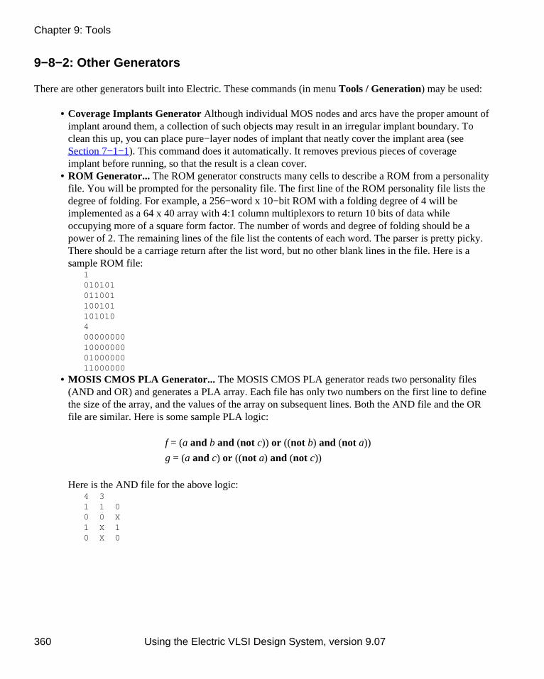
9−8−2: Other Generators
There are other generators built into Electric. These commands (in menu Tools / Generation) may be used:
Coverage Implants Generator Although individual MOS nodes and arcs have the proper amount ofimplant around them, a collection of such objects may result in an irregular implant boundary. Toclean this up, you can place pure−layer nodes of implant that neatly cover the implant area (seeSection 7−1−1). This command does it automatically. It removes previous pieces of coverageimplant before running, so that the result is a clean cover.
•
ROM Generator... The ROM generator constructs many cells to describe a ROM from a personalityfile. You will be prompted for the personality file. The first line of the ROM personality file lists thedegree of folding. For example, a 256−word x 10−bit ROM with a folding degree of 4 will beimplemented as a 64 x 40 array with 4:1 column multiplexors to return 10 bits of data whileoccupying more of a square form factor. The number of words and degree of folding should be apower of 2. The remaining lines of the file list the contents of each word. The parser is pretty picky.There should be a carriage return after the list word, but no other blank lines in the file. Here is asample ROM file: 1 010101 011001 100101 101010 4 00000000 10000000 01000000 11000000
•
MOSIS CMOS PLA Generator... The MOSIS CMOS PLA generator reads two personality files(AND and OR) and generates a PLA array. Each file has only two numbers on the first line to definethe size of the array, and the values of the array on subsequent lines. Both the AND file and the ORfile are similar. Here is some sample PLA logic:
f = (a and b and (not c)) or ((not b) and (not a))
g = (a and c) or ((not a) and (not c))
Here is the AND file for the above logic: 4 3 1 1 0 0 0 X 1 X 1 0 X 0
•
Chapter 9: Tools
360 Using the Electric VLSI Design System, version 9.07

Fill (MoCMOS)... Fill cells are used to meet metal density rules in modern fabrication processes byfilling spaces with certain metal layers. Fill cells are also created to improve chip power distributionand to avoid voltage drops by inserting cap transistors. Electric has a coverage facility to evaluate theamount of fill (see Section 9−2−4). This command generates fill cells.
•
Unlike other fill generators, Electric's fill generator creates cells containing power and ground gridsof specified layers, usually starting at Metal−2. These cells can also be arrayed into tile cells to coverlarger areas. When Metal−1 is filled, the generator will cover the area with cap transistors whosefunctionality is to prevent voltage drops in the power grid.
The Fill dialog has two tabs: "Floorplan" and "Tiling". The Floorplan section specifies what is insideof a single fill cell. The Tiling section specifies how those cells are arrayed.
The Floorplan section offers two fill techniques: Template Fill and Fill Cell (not yet available).Template Fill generates fill cells of a given width and height. The default values reflect the minimumspacing rules given by the technology. The "Reserved Space" section lets you specify which layers ofmetal will be in the fill cells. These metal layers alternate running horizontally and vertically (the"Even layer orientation" controls which layer runs horizontally first).
Chapter 9: Tools
Using the Electric VLSI Design System, version 9.07 361

The fill cell will have fourmetal wires running in eachdirection: the outer two areGround and the inner twoare Power. The spacingbetween the inner two isgiven in the "Vdd Space"section next to the selectedmetal layer. The spacingbetween the ground wiresand the edge is half of the"Gnd Space" value. Thespacing between the powerand ground wires is theminimal design−rulespacing for that layer ofmetal. The width of thewires is then adjusted to fillthe remaining space in thecell.
The Tiling section lets yourequest arrays of fill cells to begenerated. Check the desiredsizes and they will be generated.Each generated array cell willcontain the specified−size array,and it will be internally wired.
Chapter 9: Tools
362 Using the Electric VLSI Design System, version 9.07

Stitch−Based Fill Generator Similar to the previous fill generator, this stitch−based fill also createscells or tiles to meet metal density conditions, but it is a more generic tool for signal distribution.Unlike the previous tool, it allows you to generate fill cells that drive any signal, not just power andground. The fill takes a set of metal arcs stored in cells and stitches them together based on theexport names. The metal arcs can all be located in the same cell or distributed in different cells. If thearcs are in different cells, the tool will flatten all cells into one with all the signals. Networks arematched by name up to the first "_" character. For example, arcs in the networks "Vdd_1" and"Vdd_2" will be stitched together. The tool also allows you to stitch cell instances without flatteningthem; it will use the cell exports for the stitching process instead. This is the typical case for cellscontaining cap transistors.
•
There are two ways to run the tool: (1) by using a documentation cell containing the fill instructionsand issuing the Stitch−Based Fill Generator from doc input command and (2) by opening all therelevant cells in different windows and using the Stitch−Based Fill Generator from openwindows command.
When using a documentation cell to control the fill, different combinations of fill cells can begenerated at once. It also has the advantage of being easy to re−run when the fill operation must beiterated. Each line in the documentation cell follows the syntax below:
fillCellName (< options >) : cell1(< option >) cell2(< option >) ... cellN(< option >) @exports = {layerName1, layerName2}
Where option(s) can be "W" and/or a sequence of title sizes (e.g. 2x2, 4x4, 3x4). The option "W"allows the insertion of exports in the middle of the lowest metal arcs and different tile sizes can bearrayed depending on the area to cover.
By default all input cells are flattened unless option is "I". In that case, the input cell will beinstantiated instead of being flattened in the fill cell.
The @exports line specifies that exports in the generated cells should use only the layers specified. Ifthis directive is not present, exports are in the two top layers.
Chapter 9: Tools
Using the Electric VLSI Design System, version 9.07 363

Here is an example: fillAB: fillA fillB fillC(W): cap(I) fillA fillB metals45 fillD(2x4, 2x2): fillB metals45 metal6
In the example above, the first line takes the cells "fillA" and "fillB" and stitches the metal bars in"fillAB". Note that the "signalB" bars did not get stitched because the metal 2 bar does not overlap100% with the metal 3 bar. The second line generates the fill cell "fillCW" with an instance of "cap"and metal arcs from the rest of the input cells. The third line generates the cells "fillD", "fillD2x4",and "fillD2x2" where "fillD2x4" and "fillD2x2" are 2x4 and 2x2 arrays of "fillD" that contains allarcs defined in the input cells "fillB", "metals45" and "metal6".
Chapter 9: Tools
364 Using the Electric VLSI Design System, version 9.07

Generate gate layouts (MoCMOS) Generates the layout for schematic cells in the Purple and Redlibraries (see Section 9−9). To use this command you must have a schematic in the current window.The command then hierarchically scans the schematic looking for instances of the Purple and Redlibrary cells. When it finds such instances it generates layout for them and places the layout in alibrary called "autoGenLibMOCMOS". If the cell already exists, it is not regenerated.
•
The gate layout generator recognizes these gates from the Purple and Red libraries:
inv mullerC_sy nand2HTen nms2K
inv2i nand2 nand3 nms2_sy
inv2iKn nand2HLT_sy nand3LT nms3_sy3
inv2iKp nand2LT nand3LT_sy3 nor2
invCLK nand2LT_sy nand3LTen nor2kresetV
invCTLn nand2PH nand3MLT pms1
invHT nand2_sy nand3en pms1K
invK nand2en nms1 pms2
invLT nand2k nms1K pms2_sy
inv_passgate nand2LTen nms2
Chapter 9: Tools
Using the Electric VLSI Design System, version 9.07 365

Multi−Finger Transistor Cell... This command builds a cell with a multi−finger transistor (multipletransistors connected with contacts).
•
You can specify the type of transistor andcontact to use as well as the number of fingers(transistors) and the transistor size. Otheroptional factors include the pitch (extraspacing around the contacts), number of cutsin the contacts (overrides the default), andextra length of the polysilicon (gates). Thedialog on the left produces the cell on theright.
Acute Angle Fill• This command fills in cornerswhere arcs make acute angles. Thefill has a bend in the middle, andeach piece of the bend is theminimum width of the arc.
Chapter 9: Tools
366 Using the Electric VLSI Design System, version 9.07

9−9: Logical Effort
The Logical Effort tool examines a digital schematic and determines the optimal transistor size to use inorder to get maximum speed. The tool is based on the book Logical Effort, by Ivan Sutherland, Bob Sproull,and David Harris (Morgan Kaufmann, San Francisco, 1999). It is highly recommended that the user befamiliar with the concepts of this book before using the Logical Effort Tool.
To control LogicalEffort, use theLogical EffortPreferences (inmenu File /Preferences...,"Tools" section,"Logical Effort"tab). This lets youcontrol a numberof settings forLogical Effortanalysis.
Logical Effort Gates
A design that is intended to be analyzed with Logical Effort must be composed of special Logical Effortgates. A Logical Effort gate is simply a schematic or layout cell that conforms to the followingspecifications:
The cell has an attribute "LEGATE" which is set to "1". • The cell has only one output, which may have a logical effort attribute (explained below). • The cell has zero or more inputs/bidirectional ports. Each of these must have a logical effort attribute(explained below).
•
The cell has an attribute whose name does not matter, but whose value is "LE.getdrive()", and whosecode is set to "Java".
•
Chapter 9: Tools
Using the Electric VLSI Design System, version 9.07 367

On the input and output exports of the cell, we can define an attribute named "le" (use the Add LE Attributeto Selected Export command in menu Tools / Logical Effort to add this attribute). The value of thisattribute is the logical effort of that port. For example, a NAND gate typically has a logical effort on eachinput of 4/3, and an output logical effort of 2. An inverter is defined to have an input logical effort of 1, andan output logical effort of 1.
The size assigned to the logical effort gate is retrieved via the "LE.getdrive()" call. This value can then beused to size transistors within the gate. The size retrieved is scaled with respect to a minimum sized inverter(as are all other logical effort parameters). So a size of "1" denotes a minimum sized inverter.
While these attributes are defined on the layout or schematic cell definition, they must also be present on theinstantiated icon or instance of that definition. By default this will be so.
Finally, there must be at least one load that is driven by the gates in order for them to be sized. A load iseither a transistor or a capacitor. Gates that do not drive loads, or that do not drive gates that drive loads, willnot be assigned sizes.
Logical Effort Libraries
Electric comes with a set of libraries that are specially designed for Logical Effort. Use the Load LogicalEffort Libraries (Purple, Red, and Orange) command (in menu Tools / Logical Effort) to read theselibraries.
The Purple library is a set of logic gates that have been tailored for Logical Effort, as describedabove.
•
The Red library is a similar set of gates, but they are not setup for Logical Effort. The Red gates canbe used in places where Logical Effort is not to be done.
•
The Orange library is a low−level set of gates that is parameterized for a specific fabricationprocess. Orange gates are used in the Purple and Red libraries, but should not be used elsewhere. TheOrange library that comes with Electric is tailored for a generic 180 nanometer process.
•
Chapter 9: Tools
368 Using the Electric VLSI Design System, version 9.07

Advanced Features
There are several advanced features that may be added to the cell definition:
Attribute "LEKEEPER=1". This cell is defined as a keeper, whose size will be the size of thesmallest Logical Effort gate driving against it, multiplied by the Keeper Ratio.
•
Attribute "LEPARALLGRP=0". If set to 0, this gate drives by itself. If an integer greater than zero,all gates with that value whose outputs drive the same network are assumed to drive in parallel. Thesize needed to drive the load on the network will be equally divided among those gates.
•
Attribute "su=−1". This specifies the step−up (fanout) of the gate, and overrides the global fanoutspecified in the preferences. If set to −1, this attribute is ignored, and the global value is used.
•
LEWIREs
A cell marked with an attribute "LEWIRE=1" denotes a wire load. There are two ways to specify thecapacitance of an LEWIRE. The first is to use the LEWIRECAP attribute to specify the capacitance in fF.The second is to use two attributes "L" and "width" to specify the size of the wire − however this method hasbeen deprecated because it unnecessarily complicates the defintion of the Wire Ratio setting.
The LEWIRECAP is converted to X size by the following formula:
X size = LEWIRECAP * wire_ratio / x1inverter_totalgate
In this case, "wire_ratio" is defined as lambda of gate per fF of wire capacitance. "x1inverter_totalgate" is thetotal lambda of gate of an X=1 inverter, which is defined as the sum of "x1inverter_nwidth" plus"x1inverter_pwidth" (see LEsettings).
Capacitors are likewise converted to X size by the formula:
X size = Capacitance / gate_cap / 1e−15 / x1inverter_totalgate
Commands
These commands may be given to the Logical Effort tool (in menu Tools / Logical Effort):
Optimize for Equal Gate Delays Optimizes all logical effort gates (cells) to have the same delay.The delay is specified by the Global fan−out (step−up) project setting. This is NOT a pathoptimization algorithm.
•
Optimize for Equal Gate Delays (no caching) It is intended that both the caching and non−cachingalgorithms obtain exactly the same result, however due to the difficulty in obtaining and maintainingcorrectness when it comes to caching, the non−caching algorithm is also available.
•
List Info for Selected Node After running sizing, information about a specific logical effort gate canbe found by selecting the gate instance and running this command.
•
Back Annotate Wire Lengths for Current Cell Runs NCC on the current cell against it's matchinglayout or schematic cell. Assuming they match, for each LEWIRE in the schematic cell, it finds the
•
Chapter 9: Tools
Using the Electric VLSI Design System, version 9.07 369

half−perimeter of the matching wire in the layout cell (as if the layout was flattened), and thenchanges the "L" parameter on the LEWIRE to the value. Note, back−annotation is only performed ontop level LEWIREs, and it takes into account the wire's length throughout the layout hierarchy.Clear Sizes on Selected Node(s) Logical effort sizes are stored as parameters on the LEGATE.Sometimes the sheer number of sizes can overwhelm the allocated process memory, and can alsobloat file sizes when they are no longer needed. This command deletes saved sizes on a per−nodebasis.
•
Clear Sizes in all Libraries This command deletes saved sizes everywhere.• Estimate Delays This command computes load factors for every network in the cell.•
The LEsettings cell
There is a cell called LEsettings with the following attributes:
su The step−up (or fan−out) per stage.• wire_ratio The lambda of gate per fF of wire capacitance, to convert wire capacitance toequivalent gate size (see LEWIREs).
•
epsilon The convergence limit. Make smaller to get more accurate results, but requires moreiterations.
•
max_iter The maximum number of iterations the algorithm will go through before giving up.• gate_cap The fF per lambda of gate.• alpha A modulation applied to the logical effort defined on each gate's output. It is defined as theratio of diffusion capacitance to gate capacitance and it converts the output self−loading (diffusion)capacitance to equivalent units of input loading capacitance. The self−loading is calculated as:
selfXsize * outputLE * alpha
Therefore, if you set alpha to 0, the self−loading load is ignored for logical effort calculation.
•
x1inverter_length The length in lambda of the gates in a X=1 inverter.• x1inverter_nwidth The width in lambda of the nmos gate in a X=1 inverter.• x1inverter_pwidth The width in lambda of the pmos gate in a X=1 inverter.•
Chapter 9: Tools
370 Using the Electric VLSI Design System, version 9.07

9−10: Extraction
9−10−1: Parasitic Extraction
Parasitic Extraction is used by netlisters and other parts of the system that need to know about geometricfactors. Control of parasitic extraction is done with the Parasitic Preferences (in menu File / Preferences...,"Tools" section, "Parasitic" tab).
The left side of the dialog has Project Preferences. Each layer of every technology is listed, and you can setits unit resistance, area capacitance, and edge capacitance. The bottom section controls values for every layerin a technology. You can set the minimum resistance and capacitance, as well as the maximum seriesresistance. The maximum series resistance breaks long single PI models into series of distributed PI models."Include Gate In Resistance" requests that a transistor's gate area be included in overall area calculations forresistance determination. "Include Ground Network" requests that ground networks be analyzed. The "Gate
Chapter 9: Tools
Using the Electric VLSI Design System, version 9.07 371

Length Shrink" is a compensation factor for gate lengths. Some process technologies shrink the gate lengthby a fixed amount.
The right side of the dialog has User Preferences.
"Use Verbose Naming" The parasitic extractor inserts resistors, and thus makes multiple networksout of a single network. The new networks are automatically named by the netlister. Normally, thenames are simple, such as "oldnetworkname#1". When verbose naming is requested, the networknames include the nodes to which they connect, for example"oldnetworkname#m1m2conn−conn@0". This makes it possible for the user to cross−probe back tothe layout from the expanded Spice file, but it makes the file larger.
•
"Back Annotate Layout" transfers schematic net names to layout net names after NCC completes andmatches. This allows one to probe networks in layout with the same name as in the schematics,making it easier to compare schematic simulations against layout simulations.
•
"Extract Power/Ground" Always dimmed in the dialog: this feature is not available.• "Extract R" / "Extract C" allow you to uncheck one of these to remove the R or C from RC parasiticscomputations.
•
"Use exemptedNets.txt file" looks for the file 'exemptedNets.txt' in your library directory. This filespecifies nets that are exempted from simple parasitic extraction. There are two ways these nets aretreated, depending on subsequent setting: if "Extract all but exempted nets" is selected, all networksare extracted except the ones in the exempted nets file. If "Extract only exempted nets", only the netsin the exempted nets file are extracted. All nets connected to this net in subcircuits are also treatedthe same way.
•
Exempted Nets file format. One line per network. A network is specified by a library name, cell name, andnet name. When nets are not extracted, a lumped capacitance value may be specified to use on the network.This last argument is optional (0 if not specified) and ignored when the exempted nets are the only netsextracted.
libraryName cellName netName [replacementCapValue]
Example:myLib myCell{lay} net@0
myLib myCell{lay} in_a
9−10−2: Node Extraction
Because Electric captures connectivity information during design, there is no need for "node extraction", theprocess of extracting connectivity from layout. However, there are situations where a circuit has only layoutand no connectivity, specifically when a circuit has been read into Electric from CIF, GDS, or other formatsthat have no connectivity information in them (see Section 3−9−2).
When CIF, GDS, and other foreign file formats are read into Electric, the cells they create are composedentirely of pure−layer nodes (see Section 7−1−1). These nodes appear to represent the circuit correctly, andcan even be written back out to CIF or GDS correctly. But the missing connectivity information means that
Chapter 9: Tools
372 Using the Electric VLSI Design System, version 9.07

Electric cannot properly analyze these circuits (cannot do DRC, simulation, etc.)
The solution is to convert this geometry into properly connected components. To convert the current cell intoconnected geometry, use the Extract Current Cell command (from menu Tools / Network). To convert thecurrent cell and all subcells, use the Extract Current Hierarchy command. Electric creates new versions ofthe layout cells that have higher−level nodes and arcs in them.
Although the process of converting layout into connectivity information is difficult, it can usually be donecorrectly. In Electric, this process is complicated by the fact that the resulting connectivity information mustbe expressed as a set of "high−level" primitives (transistors and contacts) which have their own ways ofappearing in the layout. Therefore, it is not always possible to extract layout precisely. For example, thedesign rules for a transistor typically require that polysilicon extend beyond the gate area by 2 units, sotransistor primitives typically have this extra geometry built into them. But what would happen if thegeometry to be extracted extends by 3 units? Electric adds an extra 1−unit arc to fill−out the geometry that itfinds. Worse yet, what would happen if the geometry extends by only 1 unit? Electric simply cannotrepresent this with its primitives. It will create the transistor, but it will no longer match the originalgeometry. In general, the system attempts to create high−level primitives that mimic the original geometry. Itoften leaves small pure−layer nodes behind to complete the extraction. As an aid in debugging the extractionprocess, these extra pure−layer nodes are highlighted in the resulting cell.
Control of node extraction is done with the Network User Preferences (in menu File / Preferences..., "Tools"section, "Network" tab).
Chapter 9: Tools
Using the Electric VLSI Design System, version 9.07 373

"Grid−align to minimum technology resolution" causes all coordinates to be adjusted so that they are are notless than the minimum technology resolution given in the design rules (see Section 9−2−3). This is useful fordata that has precision problems.
"Approximate cut placement" relaxes the requirement that the cut (or via) locations appear exactly in thesame place, once extracted. When this preference is checked, Electric will find contact areas and replacethem with contact nodes regardless of where those nodes place the cuts. Without this preference, Electric willplace contact nodes in such a way that the cut layers land in the correct original locations. The disadvantageof forcing exact cut placement is that Electric will create many contact nodes, one for each cut layer. Inmulti−cut situations, this may be many more nodes than are necessary.
"Ignore polygons smaller than" limits the size of extracted polygons. When unusual geometries are extracted,there can be many tiny polygons needed to fill in gaps. By default, any polygon smaller than 1/4 unit in areais ignored.
"Use pure−layer nodes for connectivity" requests that all wires in the extracted layout be run usingpure−layer nodes. When unchecked, arcs and pins are created to make connections. Because complex layoutcan cause many little arcs and pins to be created in order to mimic the geometry, this preference lets asimpler set of pure−layer nodes do the wiring. Pure−layer nodes are harder to edit, but simpler whenmodeling complex geometry.
Active and implant regions can be handled in a number of different ways, depending on the way that theselayers are defined in the original CIF/GDS.
"Require separate N and P active; require proper select/well" assumes that there are distinct N and Pactive layers being extracted and that they are surrounded by the proper select and well layers.Extraction is easiest when all of this information is guaranteed to be correct.
•
"Ignore N vs. P active; require proper select/well" assumes that there is only one active layer for Nand P regions and so the correct select and well implants will be used to determine the type of active.
•
"Require separate N and P active; ignore select/well" assumes that the N and P active layers arecorrect, but that the implant regions are not N/P distinct and must be derived from the activeinformation.
•
"Flatten cells whose names match this" is a way to automatically flatten the hierarchy when extracting. Thisis useful in situations where parts of a node are encapsulated in subcells. For example, some designers placeall via layers into a subcell, and construct all contacts with instances of these cells. The node extractor doesnot examine subcells when extracting, and so it will not detect the contacts. By placing the subcell namesinto this field, the extractor will extract those cells and find the contacts. Note that wildcards can be usedhere.
"Flatten Cadence Pcells" requests that Cadence Pcells be flattened without having to list their names.Cadence Pcells can be recognized by the fact that their cell name ends with "$$" and a number.
Chapter 9: Tools
374 Using the Electric VLSI Design System, version 9.07

9−11: Compaction
The compaction tool squeezes layout down to minimal design−rule spacing. It does this by doing single−axiscompaction, alternating horizontal and vertical directions until no further space can be found. Each pass ofcompaction squeezes either to the left or to the bottom of the circuit.
To compact, use the Do Compaction command (in menu Tools / Compaction).
The Compaction Preferences (inmenu File / Preferences...,"Tools" section, "Compaction"tab) can tell the compactor toexpand the circuit if it is too closefor the design rules.
For an example of compaction,open the Samples library and editthe cell "tool−Compaction" (youcan read the library with the LoadSample Cells Library command,in menu Help).
Be warned that the compaction tool is experimental and doesn't always achieve optimal results.
Chapter 9: Tools
Using the Electric VLSI Design System, version 9.07 375

9−12: Silicon Compiler
Silicon compilation is the process of converting from a hardware description language (such as Verilog orVHDL) directly to placed and routed silicon. Electric has two ways of accomplishing this task. The old wayuses a silicon compilation system called QUISC (the Queen's University Interactive Silicon Compiler).
The second way, which is more modern and powerful, uses Electric's separate tools for converting hardwaredescription code, placing it, and routing it.
The Old Way: QUISC
QUISC is a powerful tool that can do placement and routing of standard cells from a schematic or a structuralVHDL description. The VHDL is compiled into a netlist which is then used to drive placement and routing.Schematics are first converted into VHDL, then compiled to a netlist and laid−out. Thus, a byproduct ofsilicon compilation will be a {net.quisc} view of a cell, and potentially a {vhdl} view.
Be warned that the silicon compiler is rather old, and so it produces layout that alternates standard cell rowsand routing rows. Modern silicon compilers use multiple metal processes to route over the standard cells, butthis system does not. This system uses two layers: a vertical routing arc to run in and out of cells, and ahorizontal routing arc to run between the cells in the routing channel. It also uses power arcs to bring powerand ground to the cell rows, and main power arcs to connect the rails on the left and right.
The VHDL description is normally placed in the "vhdl" view of a cell (see Section 4−9 for more on textediting). There is a VHDL example in cell "tool−SiliconCompiler{vhdl}" of the "samples" library. To accessit, use the Load Sample Cells Library command (in menu Help).
To convert a schematic or VHDL cell into layout, use the Convert Current Cell to Layout command (inmenu Tools / Silicon Compiler). To compile VHDL or Verilog to the {net.quisc} view, use the CompileVHDL to Netlist View or Compile Verilog to Netlist View commands. (these are typically not needed,since the previous command does it automatically).
When creating a schematic or VHDL cell to be compiled, it is important to know what primitives areavailable in the standard cell library. Electric comes with a CMOS cell library in the MOSIS CMOS("mocmos") technology. This library is not correct, and exists only to illustrate the Silicon Compiler. Thesecomponent declarations are available:
component and2 port(a1, a2 : in bit; y : out bit); end component;component and3 port(a1, a2, a3 : in bit; y : out bit); end component;component and4 port(a1, a2, a3, a4 : in bit; y : out bit); end component;component inverter port(a : in bit; y : out bit); end component;component nand2 port(a1, a2 : in bit; y : out bit); end component;component nand3 port(a1, a2, a3 : in bit; y : out bit); end component;
Chapter 9: Tools
376 Using the Electric VLSI Design System, version 9.07

component nand4 port(a1, a2, a3, a4 : in bit; y : out bit); end component;component nor2 port(a1, a2 : in bit; y : out bit); end component;component nor3 port(a1, a2, a3 : in bit; y : out bit); end component;component nor4 port(a1, a2, a3, a4 : in bit; y : out bit); end component;component or2 port(a1, a2 : in bit; y : out bit); end component;component or3 port(a1, a2, a3 : in bit; y : out bit); end component;component or4 port(a1, a2, a3, a4 : in bit; y : out bit); end component;component rdff port(d, ck, cb, reset : in bit; q, qb : out bit); end component;component xor2 port(a1, a2 : in bit; y : out bit); end component;
The Silicon Compiler Preferences (in menu File / Preferences..., "Tools" section, "Silicon Compiler" tab) letyou control many aspects of placement and routing.
The "Layout" section controls the number of rows of cells that will be created. A one−row circuitmay be exceedingly wide and short, so you may wish to experiment with this value. For a squarecircuit, the number of rows should be the square root of the number of instances in the circuit (thenumber of instances appears as the sum of the unresolved references, listed by the VHDL Compiler).
•
The "Arcs" section lets you set the horizontal and vertical routing arcs, as well as the power rails.• The "Well" section gives you the option of placing blocks of P−well and N−well over the cell rows.• The "Design Rules" section lets you control Via size, metal spacing, feed−through size, port distance,and active distance.
•
Chapter 9: Tools
Using the Electric VLSI Design System, version 9.07 377

The New Way: Individual Tools
To do silicon compilation of Verilog or VHDL using the more advanced tools, a three step process isnecessary:
Compile to a rats−nest circuit. Read in a standard cell library, and bring the hardware descriptionlanguage code (Verilog or VHDL) into a cell. Make sure to check "Make Layout Cells (notSchematics)" in the "Verilog" preferences (see Section 9−4−2). With this cell, use the ConvertCurrent Cell to Rats−Nest Structure command (in menu Tools / Silicon Compiler). Thisgenerates a cell that has all of the standard cells, placed randomly, and connected with "Unrouted"arcs.
1.
Place the cells. Now use the Floorplan and Place Current Cell command (in menu Tools /Placement). This takes the rats−nest cell and redoes the placement so that subcells are in the rightplace. You may want to set the "Run routing after placement" in the Placement Preferences. Youmay also want to set the "Padding" around placed subcells, also in the Placement Preferences.
2.
Route the cells. If you did not ask for routing after placement, you can do the routing now. Use theSea of Gates Route this Cell command (in menu Tools / Routing). If the placement system brokethe circuit into subcells (complex circuits have this happen), then you will want to route the subcellsfirst, with the Sea of Gates Route Sub−Cells command.
3.
After routing, you may want to redo the placement with different padding. You may also want to adjust therouting parameters to get better results, and you can always unroute and re−route individual networks.
Chapter 9: Tools
378 Using the Electric VLSI Design System, version 9.07

9−13: Placement
Electric has a number of placement tools that can rearrange a circuit so that routing is easier. The tools canhandle schematic or layout cells.
To run placement, use theFloorplan and Place CurrentCell command (in menu Tools /Placement). This selects anappropriate placementalgorithm to run.
For more precise control overplacement, you can select aparticular algorithm in thePlacement Preferences (in menuFile / Preferences..., "Tools"section, "Placement" tab) andthen use the Place CurrentCell with PreferredAlgorithm command. ThePlacement Preferences not onlylets you select the algorithm,but also lets you set parametersfor controlling its operation.
The bottom of the Placement Preferences dialog has controls for all placement operations. These controls seta padding percentage around each placed cell (the default is 0: make the cells touch). You can also ask theplacement system to run the Sea of Gates router after placement is done (see Section 9−6−6).
Chapter 9: Tools
Using the Electric VLSI Design System, version 9.07 379

These are the possible placement algorithms:
Algorithm Placer Notes
ForceDirected
#1Gives good results quickly (seconds). Additional time and threads does notimprove results
#2Recommended for highly−symmetric cell layouts (pads, memory), but may beunstable
row/col Useful for fixed−pitch cells
Genetic #1 / #2 Needs long runtime. Additional threads do not help
SimulatedAnnealing
#1 Not recommended for use
#2 Has best overall results. Useful for non−fixed pitch cells.
row/col Useful for fixed−pitch cells
Bottom−up partition Used to break large circuits into subproblems
Bottom−up placement Fast and good quality for placing random−sized nodes
Min−cut Simple placer that does not use multiple threads
Simple and Random Places linearly/randomly: not recommended
Chapter 9: Tools
380 Using the Electric VLSI Design System, version 9.07

Chapter 10: The JELIB and DELIB File Format
10−1: Introduction to File Format
This chapter describes Electric's native file format, which ends in "jelib". These files contain an entire libraryof cells. There are two earlier file formats which remain undocumented and are no longer recommended:"elib" is a binary format and "txt" is a text−readable format. Electric can still read and write these files, butsupport for them is limited and for legacy use only.
JELIB files are text−readable files. Each line of a JELIB file starts with an identifying character thatdistinguishes the line. Blank lines, and those that start with the comment identifying character (#) areignored. There is no limit to the length of a line of text.
After the identifying character at the start of a line, there are a set of fields. All of the fields are separated bythe separator character (|) except for the first field, which begins immediately after the identifying character.No blank spaces are allowed on a line (that is, any blank spaces are treated as valid characters). Controlcharacters (such as the identifying characters) must be upper case. In order to insert a '|' or '\n' or '\r' into afield, it must be enclosed in the quotation mark characters ("). Backslash character can be used insideenclosed strings to denote special characters:
Each of the different types of lines in the file has a fixed set of fields that must appear. Some line types alsoallow additional fields at the end to add variables (attribute/value pairs, see Section 10−4−1).
The JELIB file has 3 parts: the header, cells, and trailer.
The header has these elements:
H Header information; variable fields are allowed
V View information
L External library information
R External cell in the above external library
F External export in the above external cell
T Technology information; variable fields are allowed
O Tool information; variable fields are allowed
Using the Electric VLSI Design System, version 9.07 381
The cells have these elements:
C Cell header; variable fields are allowed
N Primitive node information in the current cell; variable fields are allowed
I Cell instance information in the current cell; variable fields are allowed
A Arc information in the current cell; variable fields are allowed
E Export information in the current cell; variable fields are allowed
X Cell termination
The trailer has this optional element:
G Group information
Everything in the file is completely ordered. There is an ordering to the external libraries, cells in thoselibraries, technologies, tools, cells, nodes/arcs/exports in a cell, etc. Even the extra variables on a line areordered. The ordering is usually a name sort. By ordering everything in the file, the exact same file isgenerated every time, and text comparison operations will accurately find differences between two files.Note, however, that the JELIB reader does not require any sorting, and can handle the data in any order.
DELIB Format
In order to enable CVS version control (see Section 6−13) Electric also has a "delib" format. This format isactually a directory (with the ".delib" extension) that contains multiple "jelib"−format files. Each of the filesin a "delib" directory contains a single view of a single cell (although it may contain multiple versions of thatcell). Instead of naming these files with the "jelib" extension, they use the cell name for their file name andthe cell view for their file extension.
The cell−files in a "delib" directory have no "V" (views), "T" (technologies), "O" (tools), or "G" (group) lines(see above). Instead, these lines appear in a separate file called "header", which also has a copy of the "H"line. Where "C" (cell) lines should appear, the "header" file contains this text:
C____SEARCH_FOR_CELL_FILES____
For example, assume that library "X" has cells A{lay}, A{sch}, and two versions of cell B{lay}: B{lay} andB;1{lay}. When written as a "jelib", all four of these cells will be stored in the file "X.jelib". When written asa "delib", there will be a directory called "X.delib" with the files "A.lay", "A.sch", "B.lay" (with two cells init), and "header".
When a cell is deleted from a library, its "delib" file is not deleted, but is retained for archival purposes. Tomark it as deleted, however, it is renamed so that it has the extension "deleted."
Chapter 10: The JELIB and DELIB File Format
382 Using the Electric VLSI Design System, version 9.07

10−2: Header
10−2−1: Header, View, and Tool
Headers
The first line in the JELIB file should be the "H" header line. The syntax is:
H<name> | <version> [ | <variable> ]*
<name> the name of the library.
<version> the version of Electric that wrote the library.
<variable> a list of variables on the library (see Section 10−4−1).
The name of the library is used in the JELIB file to identify references to this library. The actual name of thislibrary is obtained from the file path of this JELIB file.
Example:
Hlatches|8.01
Declares that library "latches" was written from Electric version 8.01.
Views
All views used in the library must be declared.
V<full name> | <name>
<full name> the full name of the view.
<name> the abbreviation name of the view.
Example:
Vlayout|lay
Declares view with abbreviation name "lay" and full name "layout".
Chapter 10: The JELIB and DELIB File Format
Using the Electric VLSI Design System, version 9.07 383

Tools
There is no need to declare all tools in the header. The only reason for a tool declaration to exist is if the toolhas project setting variables stored on it. If there are multiple tool lines, they are sorted by the tool name. Thesyntax is:
O<name> [ | <variable> ]*
<name> the name of the tool.
<variable> a list of preferences on the tool (stored as variables, see Section 10−4−1).
Example:
Ologeffort|GlobalFanout()D12.0
Declares a project setting on the "Logical Effort" tool object. The "GlobalFanout" is set to the floating pointvalue 12.
10−2−2: External References
After the header line, all external libraries cells and exports must be declared. This allows the file reader toquickly find all libraries that will be needed for the design, and to reconstruct any missing cells and exports.The cells are listed under their libraries. The exports are listed under their cells. If there are multiple externallibrary lines, they are sorted by library name; where there are multiple external cells in a library, they aresorted by their name; and where there are multiple external exports in a cell, they are sorted by their name.
The syntax of an external library reference is:
L<name> | <path>
<name> the name of the external library.
<path> the full path to the disk file with the library.
The name of the library is used in JELIB file to references to this library. The actual name of this library isobtained from the path.
The syntax of an external cell reference is:
R<name> | <lowX> | <highX> | <lowY> | <highY>
<name> the name of the external cell.
<lowX> reserved for the low X bounds of the cell contents.
<highX> reserved for the high X bounds of the cell contents.
<lowY> reserved for the low Y bounds of the cell contents.
Chapter 10: The JELIB and DELIB File Format
384 Using the Electric VLSI Design System, version 9.07

<highY> reserved for the high Y bounds of the cell contents.
The syntax of an external export reference is:
F<name> | <centerX> | <centerY>
<name> the name of the external export.
<centerX> reserved for the X coordinate of the center of export polygon.
<centerY> reserved for the Y coordinate of the center of export polygon.
Examples:
Lspiceparts|/home/strubin/electric/spiceparts.jelib
Rgate;1{sch}|−4|4|0|2
Fout|0|2
Declares that an external library called "spiceparts" will be used by the current library, and that it can befound at "/home/strubin/electric/spiceparts.jelib". In that library is a cell called "gate;1{sch}" whose contentsrun from −4 to 4 in X and 0 to 2 in Y. In that cell is an export called "out" with center at (0,2).
10−2−3: Technologies
All technologies used in the library must be in the header. The other reason for a technology declaration toexist is if the technology has preferences stored on it. If there are multiple technology lines, they are sortedby technology name. The syntax is:
T<name> [ | <variable> ]*
<name> the name of the technology.
<variable>a list of preferences on the technology (stored as variables, see Section10−4−1).
Examples:
Tmocmos
Declares that there should be a technology called "mocmos".
Tmocmos|ScaleFORmocmos()D200
Declares the technology "mocmos" and also creates a project setting on that technology object called"ScaleFORmocmos" which is a double−precision value equal to 200.
Chapter 10: The JELIB and DELIB File Format
Using the Electric VLSI Design System, version 9.07 385

10−3: Body
10−3−1: Cells
After the header information, each cell is described. A cell consists of a cell declaration ("C") followed by anumber of node ("N"), instance ("I"), arc ("A"), and export ("E") lines. The cell is terminated with a cell−endline ("X"). Inside of a cell, all nodes come first and are sorted by the node name; arcs come next and aresorted by the arc name; finally come exports, sorted by the export name. Also, when there are multiple cells,their appearance in the file is sorted by the cell name. The syntax is:
C<name> | <group> | <tech> | <creation> | <revision> | <flags> [ | <variable> ]*
<name> the name of the cell in the form "NAME;VERSION{VIEW}".
<group>the name of this cell's group (if different than expected). This field may beomitted in earlier−format libraries.
<tech> the technology of the cell.
<creation> the creation date of the cell (Java format).
<revision> the revision date of the cell (Java format).
<flags> flags for the cell.
<variable> a list of variables on the cell (see Section 10−4−1).
The Java format for dates (the creation and revision dates) is in milliseconds since the "epoch" (Midnight onJanuary 1, 1970, GMT).
The <flags> field consists of any of the following letters, (sorted alphabetically):
"C" if this cell is part of a cell−library."E" if the cell should be created "expanded"."I" if instances in the cell are locked."L" if everything in the cell is locked."T" if this cell is part of a technology−library.
Example:
CrxArray;1{lay}||mocmos|1092185029000|1092185060000|I
Declares cell "rxArray{lay}", version 1, associated with the "mocmos" technology. The cell was created atdate 1092185029000 and last modified at date 1092185060000. All instances in the cell are locked.
Chapter 10: The JELIB and DELIB File Format
386 Using the Electric VLSI Design System, version 9.07

Groups
In older JELIB files, the group information appears in special group lines. Each group line consists simply ofa list of cells in that group. The first cell listed is the "main schematics" of the group. If there is no such cell,the first field is empty. After that, the cells appear in alphabetical order. When multiple groups are declared,they appear sorted by the group name (which is derived from the cell names in it). The syntax is:
G<cell> | <cell> | ... | <cell>
<cell>the name of the cells in the group. <cell> may consists only of proto name, becauseall cells with the same base name are put into the same group.
10−3−2: Node Instances
Inside of a cell definition, node instances are declared with the "N" and "I" lines. "N" is for primitive nodesand "I" is for cell instances. All nodes are sorted by the node name. The syntax is:
N<type> | <name> | <nameTD> | <x> | <y> | <width> | <height> | <orientation> | <flags> [ |<variable> ]*
I<type> | <name> | <nameTD> | <x> | <y> | <orientation> | <flags> | <TD> [ | <variable> ]*
<type>
the type of the node instance. For primitive node instances, this has the form:[<technology>:]<primitive−node>. If <technology> is omitted, the technologyof the cell is assumed. For cell instances, it has the form:[<library>:]<cell>;<version>{<view>}. If <library> is omitted, the librarydefined by this JELIB file is assumed.
<name> the name of the node instance.
<nameTD> a text descriptor for the name (when displayed).
<x> the X coordinate of the anchor point of the node instance.
<y> the Y coordinate of the anchor point of the node instance.
<width>the difference between width of the primitive node and the standard width ofthis primitive
<height>the difference between height of the primitive node and the standard height ofthis primitive
<orientation> the orientation of the node (see below).
<flags> flags for the node instance (see below).
<TD> a text descriptor for the cell instance name (does not apply to primitives).
<variable> a list of variables on the node instance (see Section 10−4−1).
The <orientation> field is any of the following letters, followed by an optional numeric part:
Chapter 10: The JELIB and DELIB File Format
Using the Electric VLSI Design System, version 9.07 387

"X" if the node instance is X−mirrored (mirrored about Y axis)."Y" if the node instance is Y−mirrored (mirrored about X axis)."R" each letter rotates the node instance at 90 degrees counter−clockwise.Num Any digits at the end are additional rotation in tenths of a degree.
The <flags> field is any of the following letters, sorted alphabetically, followed by a numeric part:
"A" if the node instance is hard−to−select."L" if the node instance is locked."V" if the node instance is visible only inside the cell.Num Any digits at the end are the technology−specific bits.
Examples:
Nschematic:Transistor|mos@0||2|0|||R|2|ATTR_length(D5G0.5;X−0.5;Y−1;)S2
Places a schematic Transistor called "mos@0" at (2,0), standard size, rotated 90 degrees. The flag field "2" isnumeric, and therefore is technology−specific information (in this case, it makes the transistor be pMOS).There is one attribute on the node, called "length", with the value "2" (a string). This attribute is displayed,anchored at its center ("D5"), is 1 half grid unit in size ("G0.5;"), and is offset (−0.5, −1) from the node center("X−0.5;Y−1;").
Ilow;1{lay}|HAPPY||14|12|Y|A|D5G4;
Places an instance of cell "low{lay}" from the library defined in this JELIB file. The instance is named"HAPPY". It is at (14,12), mirrored in Y, and rotated 0. The "A" means that the node is hard−to−select. Itsname is described by D5G4; (D5 for a centered anchor point; G4 for 4 units size).
10−3−3: Arc Instances
Inside of a cell definition, arc instances are declared with the "A" line. All arcs are sorted by the arc name.The syntax is:
A<type> | <name> | <nameTD> | <width> | <flags> | <headNode> | <headPortID> |<headX> | <headY> | <tailNode> | <tailPortID> | <tailX> | <tailY> [ | <variable> ]*
<type>the type of the arc instance. It has the form: [<technology>:]<arc>. Iftechnology is omitted, the technology of the cell is assumed.
<name> the name of the arc instance.
<nameTD> a text descriptor for the name (when displayed).
<width>the difference between width of the arc instance and standard width of this arc'sprototype.
<flags> flags for the arc instance (see below).
<headNode> the name of the node at the head of the arc instance.
<headPortID> the ID of the port on the head node (may be blank if there are no choices).
Chapter 10: The JELIB and DELIB File Format
388 Using the Electric VLSI Design System, version 9.07

<headX> the X coordinate of the head of the arc instance.
<headY> the Y coordinate of the head of the arc instance.
<tailNode> the name of the node at the tail of the arc instance.
<tailPortID> the ID of the port on the tail node (may be blank if there are no choices).
<tailX> the X coordinate of the tail of the arc instance.
<tailY> the Y coordinate of the tail of the arc instance.
<variable> a list of variables on the arc instance (see Section 10−4−1).
The <flags> field consists of any of the following letters, sorted alphabetically, with the numeric part at theend:
"A" if the arc instance is hard−to−select."B" if the arc instance has an arrow line on the body (use "X" and "Y" for arrow heads)."F" if the arc instance is NOT fixed−angle (fixed−angle is more common)."G" if the arc instance has its head connection negated."I" if the arc instance has its head NOT extended."J" if the arc instance has its tail NOT extended."N" if the arc instance has its tail connection negated."R" if the arc instance is rigid."S" if the arc instance is slidable."X" if the arc instance has an arrow on the head (use "B" for an arrow body)."Y" if the arc instance has an arrow on the tail (use "B" for an arrow body).Num Any digits at the end are the angle of the arc (in tenths of a degree).
Examples:
AMetal−1|net@0||1|S1800|contact@0||10|10|pin@0||20|10
Places a metal−1 arc (from the technology of the cell). The arc is named "net@0", is 1 wider than standard,slidable, and at a 180 degree angle. The arc runs from (10,10) on node "contact@0", to (20,10) on node"pin@0".
Aschematic:bus|net@161|||IJ2700|busHat@4|s[1:8]|42|14|conn@15|y|42|25
Places a bus arc (from schematic) named "net@161", standard width, not end−extended on either end, at 270degrees angle. The bus runs from (42,14) on node busHat@4 (port "s[1:8]") to (42,25) on node "conn@15"(port "y").
Chapter 10: The JELIB and DELIB File Format
Using the Electric VLSI Design System, version 9.07 389

10−3−4: Exports
Inside of a cell definition, exports are declared with the "E" line. All exports are sorted by their name. Thesyntax is:
E<portID> | <name> | <TD> | <originalNode> | <originalPort> | <flags> [ | <variable> ]*
<portID> the export ID of the export.
<name> the name of the export. If empty, the <portID> field is used.
<TD> the text descriptor for writing the port (described later).
<originalNode> the name of the node instance in this cell that the export resides on.
<originalPortID>the ID of the port on the exported node instance (may be blank if there are nochoices).
<flags> flags for the export (see below).
<variable> a list of variables on the export (see Section 10−4−1).
The <flags> field has the format:<characteristics> [ /A ] [ /B ]
Where <characteristics> is the nature of the export. Choose from the following:
"U" unknown. "C2" clock phase 2.
"I" input. "C3" clock phase 3.
"O" output. "C4" clock phase 4.
"B" bi−directional. "C5" clock phase 5.
"P" power. "C6" clock phase 6.
"G" ground. "RO" reference output.
"C" clock. "RI" reference input.
"C1" clock phase 1. "RB" reference base.
/A indicates that the export is always drawn/B indicates that the export is body−only (no equivalent on the icon)
Example:
Es[18]||conn@14|a|D5G2;|I/B
Exports port "a" of node instance "conn@14" and calls it "s[18]". The text of the export is attached at thecenter of the port ("D5") and is 2 units high ("G2;"). It is of type input, and only appears in the contents (notthe icon).
Chapter 10: The JELIB and DELIB File Format
390 Using the Electric VLSI Design System, version 9.07

10−4: Miscellaneous
10−4−1: Variables
Variables may be attached to any object in the Electric database. They appear at the end of many of the linesin the file. When more than 1 variable is listed on an object, they are sorted by the variable name. The syntaxis:
<name> ( <TD> ) <type> <value>
<name> the name of the variable.
<TD> the text descriptor (when the variable is visible).
<type> the type of data attached.
<value> the data. If it starts with "[", it is an array of the form [ , , ... ]
<name> and <value> fields may be enclosed in quotation marks if the contain special characters (squarebrackets, vertical bar, double−quote, backslash, or newline). Backslash character can be used inside enclosedstrings to denote special characters (such as backslash or quote).
The <type> field can be one of these: "B" Boolean ("T" or "F")"C" Cell (of the form <library> : <cell>)"D" Double"E" Export (of the form <library> : <cell> : <exportID>)"F" Float"G" Long"H" Short"I" Integer"L" Library name"O" Tool name"P" Primitive Node prototype (of the form <technology> : <node name>)"R" Arc prototype (of the form <technology> : <arc name>)"S" String"T" Technology name"V" Point2D (of the form <x> / <y>)"Y" Byte (0−255)
Examples:
ART_message(D5G8;)StxArray4x4B
Chapter 10: The JELIB and DELIB File Format
Using the Electric VLSI Design System, version 9.07 391

Adds a variable called "ART_message" with the string "txArray4x4B". The text descriptor indicates centeredtext ("D5") that is 8 units tall ("G8;").
ART_degrees()F[0.0,3.1415927]
Adds a variable called "ART_degrees" with an array of 2 floating point values: 0.0 and 3.1415927.
EXPORTS()E[ccc:gate;1{sch}:a,"ccc:hate;1{sch}:b[0:4]"]
Adds a variable called "EXPORTS" with an array of 2 exports: export "a" of cell "ccc:gate{sch}" and export"b[0:4]" from the cell "ccc:hate{sch}".
ATTR_z0(D5G0.5;NPY1;)I50
Adds an attribute called "z0" with the integer value 50. It is displayed anchored at the center ("D5"), 0.5 unittall ("G0.5;"), written as "name=value" ("N"), is a parameter ("P"), and is offset by 1 in Y ("Y1;").
10−4−2: Text Descriptors
Text descriptors appear in every Variable, and also in other places (cell instances and exports). All textdescriptors have an anchor factor ("D0" through "D9"). If the anchor starts with a lower−case "d", the text ishidden (but the descriptor information is remembered). Here are the fields of a text descriptor:
A <size> ; Text is absolute size (in points).
B Text is bold.
C <color> ; Text is drawn in the color index given.
D0 / d0 Text is anchored at its center, limited to the size of its owner.
D1 / d1 Text is anchored at its upper−right.
D2 / d2 Text is anchored at its top.
D3 / d3 Text is anchored at its upper−left.
D4 / d4 Text is anchored at its right.
D5 / d5 Text is anchored at its center.
D6 / d6 Text is anchored at its left.
D7 / d7 Text is anchored at its lower−right.
D8 / d8 Text is anchored at its bottom.
D9 / d9 Text is anchored at its lower−left.
F <font> ; Text is shown in the named font.
G <size> ; Text has relative size (in grid units).
H Variable is inheritable (only for variables on Cells or Exports).
I Text is italic.
L Text is underlined.
N Variable is written in the form "NAME=VALUE".
OJ Text is Java code.
Chapter 10: The JELIB and DELIB File Format
392 Using the Electric VLSI Design System, version 9.07

OL Text is Spice code.
OT Text is TCL code.
P Variable is a parameter.
R Text is rotated 90 degrees.
RR Text is rotated 180 degrees.
RRR Text is rotated 270 degrees.
T Text is interior (seen only when inside the cell).
UR Value is in Resistance units.
UC Value is in Capacitance units.
UI Value is in Inductance units.
UA Value is in Current units.
UV Value is in Voltage units.
UD Value is in Distance units.
UT Value is in Time units.
X <xoff> ; Text is offset in X from object center.
Y <yoff> ; Text is offset in Y from object center.
Example:
D4G8;
The text is anchored on the left ("D4") and is 8 units tall ("G8;").
Chapter 10: The JELIB and DELIB File Format
Using the Electric VLSI Design System, version 9.07 393

10−4−3: Example
As an example of the JELIB format, let usassume a design with two levels ofhierarchy. The bottom level of hierarchy(cell "low") has 3 nodes, two arcs, and anexport, as shown here.
The top level ofhierarchy (cell "high")has two instances ofthe cell (the rightinstance is rotated 90degrees) and an arcconnecting them, asshown here.
Here is the JELIB file for the above layout:
# headerinformation: HExample|8.09
# Views:Vlayout|lay
# Technologies:Tmocmos
# Cell high;1{lay}Chigh;1{lay}||mocmos|1093555876000|1094258888640|Ngeneric:Facet−Center|art@0||0|0||||AVIlow;1{lay}|low@0||−14|12|||D5G4;Ilow;1{lay}|low@1||15|12|R||D5G4;AMetal−1|net@0|||S0|low@1|a|5|22|low@0|a|−4|22X
# Cell low;1{lay}Clow;1{lay}||mocmos|1093555232000|1094258870406|Ngeneric:Facet−Center|art@0||0|0||||AVNMetal−1−Metal−2−Con|contact@0||−10|10||||NMetal−1−Pin|pin@0||10|10||||NMetal−2−Pin|pin@1||−10|−10||||AMetal−1|net@0|||S1800|contact@0||−10|10|pin@0||10|10AMetal−2|net@1|||S900|contact@0||−10|10|pin@1||−10|−10Ea||D5G2;|pin@0||UX
Chapter 10: The JELIB and DELIB File Format
394 Using the Electric VLSI Design System, version 9.07


