Using TimeQuest Timing Analyzer 1 Introduction This tutorial provides a basic introduction to TimeQuest Timing Analyzer. It demonstrates how to set up timing constraints and obtain timing information for a logic circuit. The reader is expected to have the basic knowledge of Verilog hardware description language, as well as the basic use of the Altera Quartus II CAD software. Contents: • Introduction to timing analysis • Setting up Quartus II to use TimeQuest • Using TimeQuest • Setting Up Timing Constraints Altera Corporation - University Program January 2011 1
Transcript
Using TimeQuestTiming Analyzer
1 Introduction
This tutorial provides a basic introduction to TimeQuest Timing Analyzer. It demonstrates how to set up timingconstraints and obtain timing information for a logic circuit.
The reader is expected to have the basic knowledge of Verilog hardware description language, as well as the basicuse of the Altera Quartus II CAD software.
Contents:
• Introduction to timing analysis
• Setting up Quartus II to use TimeQuest
• Using TimeQuest
• Setting Up Timing Constraints
Altera Corporation - University ProgramJanuary 2011
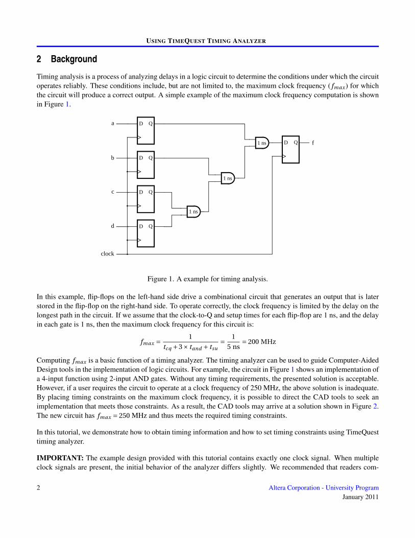
Timing analysis is a process of analyzing delays in a logic circuit to determine the conditions under which the circuitoperates reliably. These conditions include, but are not limited to, the maximum clock frequency ( fmax) for whichthe circuit will produce a correct output. A simple example of the maximum clock frequency computation is shownin Figure 1.
D Q
D Q
D Q
D Q
D Q
b
c
d
a
clock
D Q
D Q
D Q
D Q
D Q
b
c
d
a
clock
f
f
1 ns
1 ns
1 ns
1 ns
1 ns
1 ns
Figure 1. A example for timing analysis.
In this example, flip-flops on the left-hand side drive a combinational circuit that generates an output that is laterstored in the flip-flop on the right-hand side. To operate correctly, the clock frequency is limited by the delay on thelongest path in the circuit. If we assume that the clock-to-Q and setup times for each flip-flop are 1 ns, and the delayin each gate is 1 ns, then the maximum clock frequency for this circuit is:
fmax = 1
tcq +3× tand + tsu= 1
5 ns= 200 MHz
Computing fmax is a basic function of a timing analyzer. The timing analyzer can be used to guide Computer-AidedDesign tools in the implementation of logic circuits. For example, the circuit in Figure 1 shows an implementation ofa 4-input function using 2-input AND gates. Without any timing requirements, the presented solution is acceptable.However, if a user requires the circuit to operate at a clock frequency of 250 MHz, the above solution is inadequate.By placing timing constraints on the maximum clock frequency, it is possible to direct the CAD tools to seek animplementation that meets those constraints. As a result, the CAD tools may arrive at a solution shown in Figure 2.The new circuit has fmax = 250 MHz and thus meets the required timing constraints.
In this tutorial, we demonstrate how to obtain timing information and how to set timing constraints using TimeQuesttiming analyzer.
IMPORTANT: The example design provided with this tutorial contains exactly one clock signal. When multipleclock signals are present, the initial behavior of the analyzer differs slightly. We recommended that readers com-
2 Altera Corporation - University ProgramJanuary 2011
Figure 2. Functionally equivalent circuit with a different logic structure.
plete the tutorial using the provided example design before proceeding to use TimeQuest on their own design. Weelaborate on this issue in Section 6.
3 Design Example
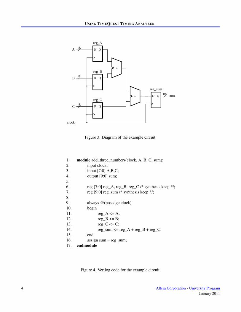
As an example we will use an adder that adds three 8-bit numbers and produces a sum output. The inputs are A, B ,and C , which are stored in registers reg_A, reg_B and reg_C at the positive edge of the clock. The three registersprovide inputs to the adder, whose result is stored in the reg_sum register. The output of the reg_sum register drivesthe output port sum. The diagram of the circuit is shown in Figure 3.
The Verilog source code for the design is given in Figure 4. Note that the ”synthesis keep” comment is included inthis code. This comment is interpreted as a directive that instructs Quartus II software to retain the specified nodesin the final implementation of the circuit and keep their names as stated. This directive will allow us to refer to thesenodes in the tutorial.
To begin the tutorial open the example project. It is available in the add_three_numbers directory provided with thistutorial.
Compile the example circuit to see the results of timing analysis. These results will be available in the compilationreport, once the design is compiled. In this tutorial we will use the TimeQuest Graphical User Interface to inspectthe timing analysis results.
Altera Corporation - University ProgramJanuary 2011
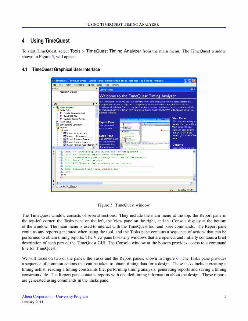
To start TimeQuest, select Tools > TimeQuest Timing Analyzer from the main menu. The TimeQuest window,shown in Figure 5, will appear.
4.1 TimeQuest Graphical User Interface
Figure 5. TimeQuest window.
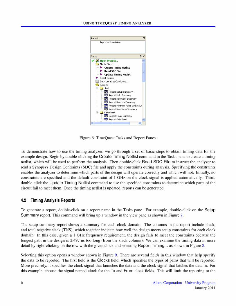
The TimeQuest window consists of several sections. They include the main menu at the top, the Report pane inthe top-left corner, the Tasks pane on the left, the View pane on the right, and the Console display at the bottomof the window. The main menu is used to interact with the TimeQuest tool and issue commands. The Report panecontains any reports generated when using the tool, and the Tasks pane contains a sequence of actions that can beperformed to obtain timing reports. The View pane hosts any windows that are opened, and initially contains a briefdescription of each part of the TimeQuest GUI. The Console window at the bottom provides access to a commandline for TimeQuest.
We will focus on two of the panes, the Tasks and the Report panes, shown in Figure 6. The Tasks pane providesa sequence of common actions that can be taken to obtain timing data for a design. These tasks include creating atiming netlist, reading a timing constraints file, performing timing analysis, generating reports and saving a timingconstraints file. The Report pane contains reports with detailed timing information about the design. These reportsare generated using commands in the Tasks pane.
Altera Corporation - University ProgramJanuary 2011
To demonstrate how to use the timing analyzer, we go through a set of basic steps to obtain timing data for theexample design. Begin by double-clicking the Create Timing Netlist command in the Tasks pane to create a timingnetlist, which will be used to perform the analysis. Then double-click Read SDC File to instruct the analyzer toread a Synopsys Design Contraints (SDC) file and apply the constraints during analysis. Specifying the constraintsenables the analyzer to determine which parts of the design will operate correctly and which will not. Initially, noconstraints are specified and the default constraint of 1 GHz on the clock signal is applied automatically. Third,double-click the Update Timing Netlist command to use the specified constraints to determine which parts of thecircuit fail to meet them. Once the timing netlist is updated, reports can be generated.
4.2 Timing Analysis Reports
To generate a report, double-click on a report name in the Tasks pane. For example, double-click on the SetupSummary report. This command will bring up a window in the view pane as shown in Figure 7.
The setup summary report shows a summary for each clock domain. The columns in the report include slack,and total negative slack (TNS), which together indicate how well the design meets setup constraints for each clockdomain. In this case, given a 1 GHz frequency requirement, the design fails to meet the constraints because thelongest path in the design is 2.497 ns too long (from the slack column). We can examine the timing data in moredetail by right-clicking on the row with the given clock and selecting Report Timing... as shown in Figure 8.
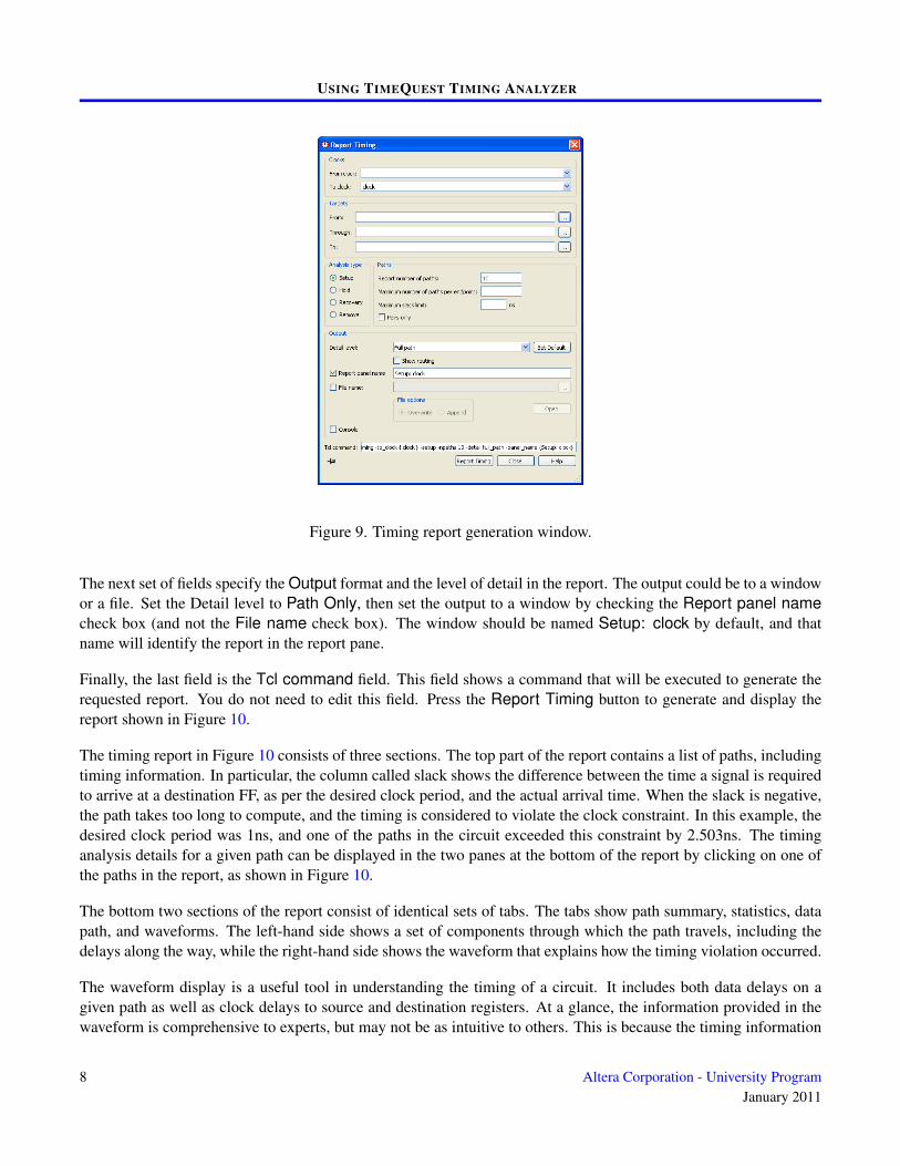
Selecting this option opens a window shown in Figure 9. There are several fields in this window that help specifythe data to be reported. The first field is the Clocks field, which specifies the types of paths that will be reported.More precisely, it specifies the clock signal that launches the data and the clock signal that latches the data in. Forthis example, choose the signal named clock for the To and From clock fields. This will limit the reporting to the
6 Altera Corporation - University ProgramJanuary 2011
Figure 8. Pop-up menu to generate a detailed timing report.
register-to-register paths only.
The next field is the Targets field. The Targets field further refines the report by focusing only on certain paths inthe design. We can specify the starting and the ending point of the paths of interest by filling the From and To fields.In addition, we can look at only the paths that pass through certain nodes in the design. For this example, we leavethese fields blank to indicate that every path should be taken into account for the report.
The next two fields are the Analysis type and Paths fields. The Analysis type field specifies if the report shouldcontain setup, hold, recovery, or removal information. Each of these analyses looks for distinct timing characteristicsin your design. For example, the setup analysis determines if the data arrives at a flip-flop sufficiently early for theflip-flop to store it reliably, given a clock period. On the other hand, the hold analysis determines if the data inputat any given flip-flop remains stable after the positive edge of the clock long enough for the data to be stored in aflip-flop reliably. The Paths field specifies the maximum number of paths to be reported and the maximum slackrequired for a path to be included in the report. For this example, choose the type of analysis to be Setup and select10 paths to be reported. This will generate a setup analysis report and show 10 paths with largest negative slack (thepaths that violate the constraint the most).
Altera Corporation - University ProgramJanuary 2011
The next set of fields specify the Output format and the level of detail in the report. The output could be to a windowor a file. Set the Detail level to Path Only, then set the output to a window by checking the Report panel namecheck box (and not the File name check box). The window should be named Setup: clock by default, and thatname will identify the report in the report pane.
Finally, the last field is the Tcl command field. This field shows a command that will be executed to generate therequested report. You do not need to edit this field. Press the Report Timing button to generate and display thereport shown in Figure 10.
The timing report in Figure 10 consists of three sections. The top part of the report contains a list of paths, includingtiming information. In particular, the column called slack shows the difference between the time a signal is requiredto arrive at a destination FF, as per the desired clock period, and the actual arrival time. When the slack is negative,the path takes too long to compute, and the timing is considered to violate the clock constraint. In this example, thedesired clock period was 1ns, and one of the paths in the circuit exceeded this constraint by 2.503ns. The timinganalysis details for a given path can be displayed in the two panes at the bottom of the report by clicking on one ofthe paths in the report, as shown in Figure 10.
The bottom two sections of the report consist of identical sets of tabs. The tabs show path summary, statistics, datapath, and waveforms. The left-hand side shows a set of components through which the path travels, including thedelays along the way, while the right-hand side shows the waveform that explains how the timing violation occurred.
The waveform display is a useful tool in understanding the timing of a circuit. It includes both data delays on agiven path as well as clock delays to source and destination registers. At a glance, the information provided in thewaveform is comprehensive to experts, but may not be as intuitive to others. This is because the timing information
8 Altera Corporation - University ProgramJanuary 2011
Figure 10. Detailed setup time information for a given register-to-register path.
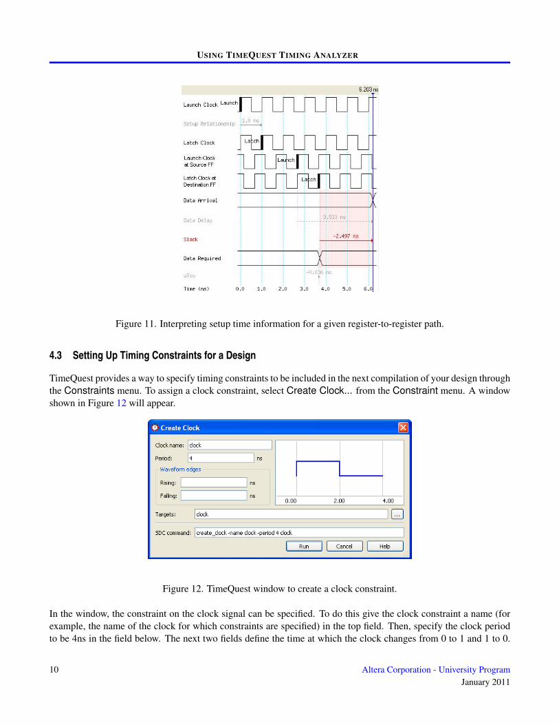
is shown with respect to the time when inputs appear at the input pin to an FPGA device. For example, the clocksignal shown in the first line is the signal at the pin of the device, and it arrives at the clock input of the sourceflip-flop later. In Figure 11 we show how to interpret the waveform information presented in Figure 10.
In the figure, the first three waveforms show the clock signals for the source and destination flop-flops, along with atiming requirement - in this case 1ns. The launch and latch edges of each clock are indicated by thick lines. The nexttwo waveforms in the figure show the same clock signals as they appear at the clock inputs of source and destinationflip-flops, with the launch and latch clock edges indicated appropriately. These two waveforms show the actual timethe data will be launched from and stored in flip-flops. Note that the Launch Clock at Source FF and Latch Clock atDestination FF waveforms in Figure 11 are shown for this explanation, but are not part of the screenshot in Figure 10.The Clock Delay in Figure 10 represents the time between the launch/latch edges at the pin of the device and at theclock inputs of the source/destination flip-flops.
The next two waveforms, Data Arrival and Data Delay, show the time it will take a signal to propagate from sourceto destination. Notice that Data Delay is measured from the positive edge of the clock named Launch Clock atSource FF. The second last waveform, called Data Required indicates the time when the data should have arrivedat the destination flip-flop to be stored correctly, including the setup time (uTsu) shown in the last line.
From the diagram we see that the time the data arrives at its destination is after the time it is required to arrive if itis to meet the timing constraint. Thus, the timing constraint is violated. To indicate this, a negative slack value isshown to indicate by how much the timing constraint is violated. In contrast, a timing constraint that is satisfied hasa positive slack value.
Altera Corporation - University ProgramJanuary 2011
Figure 11. Interpreting setup time information for a given register-to-register path.
4.3 Setting Up Timing Constraints for a Design
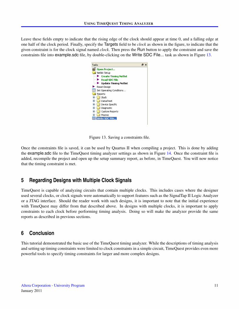
TimeQuest provides a way to specify timing constraints to be included in the next compilation of your design throughthe Constraints menu. To assign a clock constraint, select Create Clock... from the Constraint menu. A windowshown in Figure 12 will appear.
Figure 12. TimeQuest window to create a clock constraint.
In the window, the constraint on the clock signal can be specified. To do this give the clock constraint a name (forexample, the name of the clock for which constraints are specified) in the top field. Then, specify the clock periodto be 4ns in the field below. The next two fields define the time at which the clock changes from 0 to 1 and 1 to 0.
10 Altera Corporation - University ProgramJanuary 2011
Leave these fields empty to indicate that the rising edge of the clock should appear at time 0, and a falling edge atone half of the clock period. Finally, specify the Targets field to be clock as shown in the figure, to indicate that thegiven constraint is for the clock signal named clock. Then press the Run button to apply the constraint and save theconstraints file into example.sdc file, by double-clicking on the Write SDC File... task as shown in Figure 13.
Figure 13. Saving a constraints file.
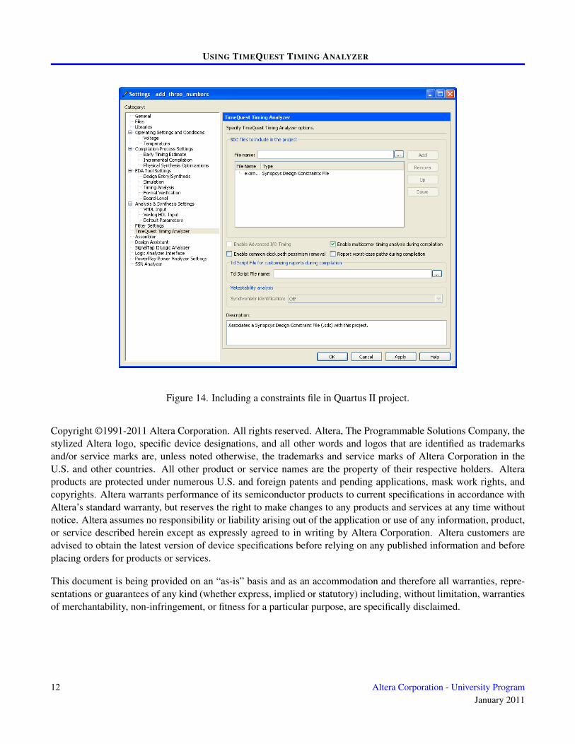
Once the constraints file is saved, it can be used by Quartus II when compiling a project. This is done by addingthe example.sdc file to the TimeQuest timing analyzer settings as shown in Figure 14. Once the constraint file isadded, recompile the project and open up the setup summary report, as before, in TimeQuest. You will now noticethat the timing constraint is met.
5 Regarding Designs with Multiple Clock Signals
TimeQuest is capable of analyzing circuits that contain multiple clocks. This includes cases where the designerused several clocks, or clock signals were automatically to support features such as the SignalTap II Logic Analyzeror a JTAG interface. Should the reader work with such designs, it is important to note that the initial experiencewith TimeQuest may differ from that described above. In designs with multiple clocks, it is important to applyconstraints to each clock before performing timing analysis. Doing so will make the analyzer provide the samereports as described in previous sections.
6 Conclusion
This tutorial demonstrated the basic use of the TimeQuest timing analyzer. While the descriptions of timing analysisand setting up timing constraints were limited to clock constraints in a simple circuit, TimeQuest provides even morepowerful tools to specify timing constraints for larger and more complex designs.
Altera Corporation - University ProgramJanuary 2011
This document is being provided on an “as-is” basis and as an accommodation and therefore all warranties, repre-sentations or guarantees of any kind (whether express, implied or statutory) including, without limitation, warrantiesof merchantability, non-infringement, or fitness for a particular purpose, are specifically disclaimed.
12 Altera Corporation - University ProgramJanuary 2011