90
USPIIi-1v Software Manual Revision B2

USPIIi-1v
Software Manual
Revision B2


Themis Computer—Rest of World20 rue du Tour de l’Eau 38400 St Martin d’Heres, FrancePhone +33 476 59 60 46Fax +33 476 59 60 49
Themis Computer—Americas and Pacific Rim3185 Laurelview CourtFremont, CA 94538, USAPhone (510) 252-0870Fax (510) 490-5529World Wide Web http://www.themis.com
USPIIi-1v Software ManualVersion B2 — December 2001
Copyright © 2000 Themis Computer, Inc.
ALL RIGHTS RESERVED. No part of this publication may be reproduced in any form, byphotocopy, microfilm, retrieval system, or by any other means now known or hereafter invented withoutthe prior written permission of Themis Computer.
The information in this publication has been carefully checked and is believed to be accurate. However,Themis Computer assumes no responsibility for inaccuracies. Themis Computer retains the right tomake changes to this publication at any time without prior notice. Themis Computer does not assumeany liability arising from the application or use of this publication or the product(s) described herein.
RESTRICTED RIGHTS LEGEND: Use, duplication, or disclosure by the United States Governmentis subject to the restrictions set forth in DFARS 252.227-7013 (c)(1)(ii) and FAR 52.227-19.
TRADEMARKS
SOLARIS™ is a registered trademark of Sun Microsystems
SPARC™ is a registered trademark of SPARC International
All other trademarks used in this publication are the property of their respective owners.
USPIIi-1v Software Manual
December 2001
Part Number: 108966
Themis Customer Support
North America, South America, and Pacific Rim
Telephone: 510-252-0870Fax: 510-490-5529
E-mail: [email protected] Site: http://www.themis.com

Version Revision History
Version B2) December 2001Realigned page numbers in Table of Contents to right-hand margin.Changed 31 to 33 in Figure 2-7, page 2-10.Replaced garbled text in Table 3-6 footnote-a (page 3-9) to “3-3”.Replaced READY_LED with USER_LED in Table 6-2, page 6-3.
Version B1) July 20, 2000Corrected boot addresses in table 3-11 and added programming of User FLASH 2 in table 7-2
Version B) May 25, 2000New sections added
Version A) August 3, 1998Initial Engineering version of document.


Table of Contents
Table of Contents
How to Use This Manual Introduction ..................................................................................................................... 1-1Intended Audience .......................................................................................................... 1-1In Case Of Difficulties .................................................................................................... 1-1
UltraSPARC-IIi CPU Description Introduction ..................................................................................................................... 2-1Processor Description ..................................................................................................... 2-1
PCI Bus Module (PBM) ................................................................................. 2-2Memory Management Unit (MMU) ............................................................... 2-2I/O Memory Management Unit (IOM) ........................................................... 2-2External Cache Controller Unit (ECU) ........................................................... 2-2Memory Controller Unit (MCU) .................................................................... 2-3Instruction and Data Cache (I- and D- Cache) ............................................... 2-3Prefetch and Dispatch Unit (PDU) ................................................................. 2-3Integer Execution Unit (IEU) ......................................................................... 2-3Floating-Point Unit (FPU) .............................................................................. 2-4Load/Store Unit (LSU) ................................................................................... 2-4
PCI Bus Interface Modules (PBM) ................................................................................. 2-4Unsupported PCI Features .............................................................................. 2-5PCI Bus Operations ........................................................................................ 2-5
Transaction Termination................................................................. 2-5Read/Write Cycles .......................................................................................... 2-5Endian-ness ..................................................................................................... 2-6
Big-endian and Little- endian Address Space ................................. 2-6Memory Management Units (MMU) ............................................................................. 2-6
Themis Computer i
USPIIi-1v Software Manual
Virtual Address Translation ............................................................................ 2-7I/O Memory Management Unit (IOM)........................................................................... 2-8
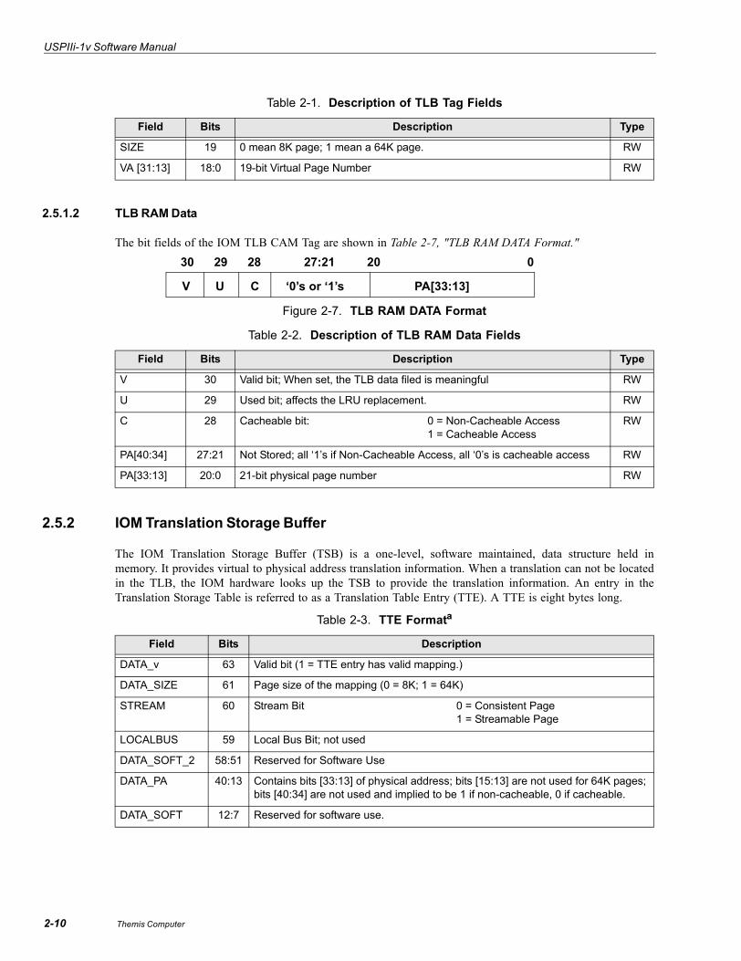
IOM Translation Look-Aside Buffer (TLB) ................................................... 2-9TLB CAM Tag................................................................................ 2-9TLB RAM Data ............................................................................ 2-10
IOM Translation Storage Buffer ................................................................... 2-10Translation Errors ......................................................................... 2-11
Instruction and Data Cache ........................................................................................... 2-11I-Cache ....................................................................................................... 2-11D-Cache ....................................................................................................... 2-12LSU_Control_Register ................................................................................. 2-12
Themis USPIIi-1V address MapIntroduction ..................................................................................................................... 3-1USPIIi-1V Address Map ................................................................................................. 3-1PCI Address Map ............................................................................................................ 3-2List of PCI devices .......................................................................................................... 3-2Physical Memory Address Range ................................................................................... 3-3UltraSPARC-IIi PCI Control and Status Registers ......................................................... 3-4Advanced PCI Bridge (APB) configuration space registers ........................................... 3-7PCI Bridge 21150 Registers ........................................................................................... 3-9UNIVERSE II VME Interface Registers ...................................................................... 3-10Ultra Fast/Wide SCSI Controller (SYMBIOS SYM53C876) ...................................... 3-17PCIO Controller Address Map ..................................................................................... 3-18PCIO (CHEERIO) #1 EBUS Device Mapping ............................................................ 3-20PCIO(CHEERIO) #2 EBUS Device Mapping ............................................................. 3-21VMEbus Reset Register................................................................................................. 3-21
UNIVERSE II: PCI-VME bridgeIntroduction ..................................................................................................................... 4-1Universe as VME Bus Slave ........................................................................................... 4-1
Slave VME Write transactions ....................................................................... 4-3Slave VME Read transactions ........................................................................ 4-3
Terminations ................................................................................... 4-3Universe as VMEbus Master .......................................................................................... 4-4
Coupled Transfers ........................................................................................... 4-7Posted Writes .................................................................................................. 4-8Terminations ................................................................................................... 4-9
Target-Disconnect ........................................................................... 4-9Target-Retry..................................................................................... 4-9Target-Abort ................................................................................... 4-9
Universe DMA controller ............................................................................................. 4-10Universe as a VME Requester ...................................................................................... 4-10
ii Themis Computer

Table of Contents
Requesting VMEbus ..................................................................................... 4-10Releasing VMEbus ....................................................................................... 4-11
VME Cycle Terminations ............................................................................................. 4-11Universe as a System Controller ................................................................................... 4-11
VMEbus Configuration-First Slot Detector .................................................. 4-11VMEbus time out .......................................................................................................... 4-12Using OBP to program VME Interface ........................................................................ 4-13
OBP commands ............................................................................................ 4-13OBP Environment variables ......................................................................... 4-14
USPIIi-1V Interrupts Overview ......................................................................................................................... 5-1Mondo Dispatch Overview.............................................................................................. 5-2UltraSPARCIIi Interrupt Registers ................................................................................. 5-2
Interrupt Mapping Registers ........................................................................... 5-3Interrupt Vector Data Register ........................................................................ 5-3Clear Interrupt Register .................................................................................. 5-4
Interrupt Level Mapping ................................................................................................. 5-4VMEbus Interrupts handling .......................................................................................... 5-5
VxWorks implementation ............................................................................... 5-5Solaris implementation ................................................................................... 5-6
FPGA, Watchdog and Temperature Sensors Registers FPGA and Watchdog Registers ...................................................................................... 6-1
Introduction..................................................................................................... 6-1FPGA Status Register ..................................................................................... 6-33-Level Watchdog Registers ........................................................................... 6-3
Temperature Sensor Registers ........................................................................................ 6-4Temperature Sensor Implementation .............................................................. 6-4Interfacing the Temperature Sensor through OBP ......................................... 6-5
Themis USPIIi-1V SoftwareIntroduction ..................................................................................................................... 7-1SUN OBP (Open Boot Prom) ......................................................................................... 7-1
Description of OBP VME Environment Variables ......................................... 7-2Support Commands ......................................................................................... 7-3
probe-scsi-all ................................................................................... 7-3test net2 .................................................................................... 7-3Updating the System and User FLASH .......................................... 7-3
Additional OBP commands ............................................................................ 7-4Accessing VME from OBP ............................................................. 7-4OBP Device aliases ......................................................................... 7-6
VxWorks Firmware ........................................................................................................ 7-7SUN Solaris .................................................................................................................... 7-7
Themis Computer iii

USPIIi-1v Software Manual
Installing the USPIIi-1V VME Nexus driver ................................................. 7-8Installing THEMISvme................................................................... 7-8
Sample VME Programs and VME leaf drivers .............................................. 7-8
iv Themis Computer
List of Tables
List of Tables
Table 2-1. Description of TLB Tag Fields ............................................................................................. 2-9Table 2-2. Description of TLB RAM Data Fields ................................................................................ 2-10Table 2-3. TTE Format ......................................................................................................................... 2-10Table 2-4. LSU_Control_Register ........................................................................................................ 2-12Table 3-1. UltraSPARC-IIi Address Map............................................................................................... 3-1Table 3-2. Physical address space to PCI space .................................................................................... 3-2Table 3-3. List of PCI Devices ............................................................................................................... 3-2Table 3-4. Physical Memory Address Range ......................................................................................... 3-3Table 3-5. CSR Register address Space.................................................................................................. 3-4Table 3-6. APB Configuration Space Registers ..................................................................................... 3-8Table 3-7. PCI Bridge Registers ............................................................................................................. 3-9Table 3-8. Universe II Register Map .................................................................................................... 3-11Table 3-9. SCSI Controller Registers ................................................................................................... 3-17Table 3-10. PCIO Registers .................................................................................................................. 3-19Table 3-11. PCIO #1 EBUS device mapping ....................................................................................... 3-20Table 3-12. PCIO #2 EBUS device mapping ....................................................................................... 3-21Table 3-13. VMEbus Reset Registe...................................................................................................... 3-21Table 4-1. VSIx_CTL Register Description ........................................................................................... 4-2Table 4-2. VSIx_BS Register Description.............................................................................................. 4-2Table 4-3. VSIx_BD Register Description ............................................................................................. 4-2Table 4-4. VSIx_TO Register Description ............................................................................................. 4-2Table 4-5. LSIx_CTL Register Description ........................................................................................... 4-4Table 4-6. LSIx_BS Register Description .............................................................................................. 4-5Table 4-7. LSIx_BD Register Description ............................................................................................. 4-5Table 4-8. LSIx_TO Register Description.............................................................................................. 4-5Table 4-9. MISC_CTL Register ........................................................................................................... 4-13Table 4-10. OBP Variables for VME Control ...................................................................................... 4-14Table 5-1. Interrupt Mapping register definition .................................................................................... 5-3
Themis Computer v

USPIIi-1v Software Manual
Table 5-2. Interrupt Receive Data Register ............................................................................................ 5-3Table 5-3. Clear Interrupt Register ......................................................................................................... 5-4Table 5-4. Interrupt level mapping ......................................................................................................... 5-4Table 6-1. FPGA Internal Register Address Map................................................................................... 6-2Table 6-2. FPGA Status Register............................................................................................................ 6-3Table 6-3. Temperature Sensor Configuration and Status Register Definition ...................................... 6-4Table 6-4. Temperature Sensor OBP Commands................................................................................... 6-5Table 7-1. OBP VME Environment Variables ....................................................................................... 7-2Table 7-2. Flash-update command syntax .............................................................................................. 7-3Table 7-3. Additional OBP Commands .................................................................................................. 7-4Table 7-4. List of OBP aliases ................................................................................................................ 7-6
vi Themis Computer

List of Figures
List of Figures
Figure 2-1. UltraSPARC-IIi Floating Point Register.............................................................................. 2-4Figure 2-2. UltraSPARC-IIi Virtual Address Space with VA Hole ....................................................... 2-7Figure 2-3. Software view of the UltraSPARC-IIi MMU ...................................................................... 2-8Figure 2-4. Virtual to Physical Address Translation for an 8 KB Page.................................................. 2-9Figure 2-5. Virtual to Physical Address Translation for a 64 KB Page.................................................. 2-9Figure 2-6. TLB CAM Tag Format ........................................................................................................ 2-9Figure 2-7. TLB RAM DATA Format ................................................................................................. 2-10Figure 3-1. UCSR Access Mechanism ................................................................................................. 3-11Figure 4-1. VMEbus Slave Channel Dataflow. ...................................................................................... 4-3Figure 4-2. Influence of Transaction data width and target Image data width ....................................... 4-6Figure 4-3. Universe is sampling IACK rather than IACKIN.............................................................. 4-12Figure 5-1. Interrupt Logic. .................................................................................................................... 5-2
Themis Computer vii

USPIIi-1v Software Manual
viii Themis Computer

11How to Use This Manual
1.1 Introduction
The Themis Computer USPIIi-1v is a UltraSPARC-IIi based single-board VMEbus computer. The software interface for the VMEbusand other on-board peripheral devices is transparently implemented under Solaris. Themis Computer has also developed customsoftware that enables software programmers to effectively use the powerful features of the VMEbus Interface.
1.2 Intended Audience
The custom software containing programs, documentation, and packaging, is targeted for various softwareusers:
• System Administrators who install the software and perform the necessary software configuration• Users who perform day-to-day operations on USPIIi-1v systems• Application programmers who write user-level programs to access the VMEbus interface devices
through the built-in VMEbus devices. These devices are listed in .• System programmers / device driver writers who develop kernel-level device drivers for VMEbus
devices
Some functions overlap one another. The basic concepts required for many of these functions are common.This manual is structured around the basic concepts of using a VMEbus system.
1.3 In Case Of Difficulties
If the USPIIi-1v does not behave as described or if you encounter difficulties installing or configuring theboard please call Themis Computer technical support at +1 (510) 252-0870, fax your questions to +1 (510)490-5529, or e-mail to [email protected]. You can also contact us via our web site: www.themis.com.
Themis Computer 1-1

USPIIi-1v Software Manual
1-2 Themis Computer

22 UltraSPARC-IIi CPU Description
2.1 Introduction
This chapter is intended to provide a basic description of the UltraSPARC-IIi processor, a 64-bit, SPARC-V9-compliant processor. The UltraSPARC-IIi meets the requirements of PCI specification, version 2.1. TheUltraSPARC-IIi processor is the core of the USPIIi-1v board and provides a balanced price-performancesolution delivering, at a reasonable cost, the power and features required by a majority of high-endapplications. The UltraSPARC-IIi optimizes power consumption and manufacturability, making the USPIIi-1v an ideal choice for VME based projects.
The UltraSPARC-IIi is a high-performance, highly integrated, superscalar processor. The decentralizedcontrol of the UltraSPARC-IIi’s functional areas enables the processor to complete up to 4 instructions percycle, even in the presence of conditional branches and cache misses. Each functional area operatesindependently.
Some of the features of the UltraSPARC-IIi are:• 9-stage integer instruction pipeline with a 3-stage addition for floating-point pipeline synchronization • Instructions before and after conditional branches• Parallel, out of order instruction execution• Multiple, separate functional units• Load buffers on the input side of the Execution Unit and store buffers on the output side of the
Execution decouple the execution pipeline from data cache misses.• Separate Memory Control and I/O interface units decouple their related activities from the processor
pipeline.
2.2 Processor Description
Through the UltraSPARC-IIi the USPIIi-1v provides the following functionality:• Independently clocked (132 MHz internal, 66 or 33 MHz external) PCI interfaces, fully decoupled from
the CPU.• PCI Bus Module (PBM)
Themis Computer 2-1
USPIIi-1v Software Manual
• PCI I/O Memory Management unit (IOM) with 16 incoming I/O physical/mapping protection entries.• External Cache (E-Cache) Controller (ECU)• Memory Controller Unit (MCU)• 16 KB Instruction Cache (I-Cache)• 16 KB Data Cache (D-Cache)• 64-entry instruction translation lookaside buffer (iTLB) and a 64-entry data translation lookaside buffer
(dTLB)• Prefetch and Dispatch Unit (PDU) prefetches instructions before they are needed.• Integer Execution Unit (IEU) with two arithmetic logic units (ALUs)• Floating-point Unit (FPU) with independent add, multiply and divide/square root sub-units• Graphics Unit (GRU) composed of two independent execution pipelines• Load, buffer and store unit (LSU), decoupling data accesses from the pipeline.
2.2.1 PCI Bus Module (PBM)
The PBM interfaces directly with a 32-bit, 64 MHz PCI bus, is optimized for 16-, 32-, and 64-bit transfersand can support up to four (4) masters. The PBM generates memory, I/O, and configuration read and writecycles.
The entire PCI address space is non-cacheable for CPU references, but coherent DMA is supported. All writesto memory from the PCI bus and all reads from memory are cache coherent. For more information on thePBM, refer to Section 2.3, "PCI Bus Interface Modules (PBM)," on page 2-4.
2.2.2 Memory Management Unit (MMU)
The Memory Management Unit translates 44-bit virtual addresses to 41-bit physical addresses for all accessesto memory by the UltraSPARC-IIi. The UltraSPARC-IIi MMU conforms to the requirements of the SPARCArchitecture Manual, Version 9. For more information on the MMU, refer to Section 2.4, "MemoryManagement Units (MMU)," on page 2-6.
2.2.3 I/O Memory Management Unit (IOM)
The I/O Memory Management Unit (IOM) performs virtual to physical address translation for all DVMAcycle. The UltraSPARC-IIi MMU is bypassed in DVMA cycles. The PCI master provides a 32-bit virtualaddress which to IOM translates to a 34-bit physical address. For more information on the IOM, refer toSection 2.5, "I/O Memory Management Unit (IOM)," on page 2-8.
2.2.4 External Cache Controller Unit (ECU)
The ECU handles misses to the Instruction Cache (I-Cache) and Data Cache (D-Cache) by efficientlymanaging accesses to the External Cache (E-Cache). The ECU can handle one (1) access to the E-Cacheevery other processor clock cycle. A miss in the D-Cache will cause a 16-Byte D-Cache fill through two (2)consecutive 8-byte E-Cache access (four processor cycles). A miss in the I-Cache will cause a 32-byte I-Cache fill using four (4) consecutive E-Cache accesses (eight processor cycles). All stores to the E-Cache arewrite-through and fully pipelined. The E-Cache is parity-protected.
2-2 Themis Computer

2. UltraSPARC-IIi CPU Description
Additionally, the ECU supports DMA accesses which hit the E-Cache. Data coherency is maintained betweenthe 2 MB E-Cache and main memory as well as between all caches and external PCI DMA references.
Block loads and stores can provide a very high transfer bandwidth by loading or storing a 64-byte line of datafrom memory or E-Cache to the floating-point register file. To avoid polluting the E-Cache with large, singleaccess data block, block loads and stores are not installed in the E-cache.
2.2.5 Memory Controller Unit (MCU)
All transactions to the DRAM and UPA64S subsystems, including the Creator Graphics card and the Themisproprietary memory modules are controlled by the MCU. The UPA64S bus runs at 1/4 of the rate of theUltraSPARC-IIi processor clock. Depending on the grade of processor ordered this will either be at 110 MHz,for the 440 MHz processor, or 90 MHz, for the 360 MHz processor.
The data transfer to the memory modules occurs at 1/4 of the UltraSPARC-IIi processor frequency, either 110MHz for the 440 MHz processor, or 90 MHz for the 360 MHz processor. The USPIIi-1v uses externaltransceivers (Texas Instruments SN74ALVC16268: Bidirectional Registered 12-bit-to-24-bit bus exchanger)to increase the memory module data bus to twice the width as the UltraSPARC-IIi’s memory bus.
2.2.6 Instruction and Data Cache (I- and D- Cache)
The I-Cache is 16 KB two-way set-associative cache with 32-byte blocks. The I-Cache is physically indexedand physically tagged. The D-Cache is a write-through, non-allocating-on-write-miss, 16 KB direct-mappedcache with two 16-byte sub-blocks per line. The D-Cache is virtually indexed and physically tagged. TheLSU_Control_Register contains fields that control the hardware functions of the I-Cache, D-Cache, MMU(TLBs), bad parity generation, and watchpoint settings.
2.2.7 Prefetch and Dispatch Unit (PDU)
The PDU fetches instructions before they are needed so that the execution unit is not starved for instructions.Instructions can be prefetched from all levels of memory including the I-Cache, E-Cache, and main memory.To predict conditional branches a dynamic two-bit, instruction history based on the branch is implemented inhardware. The “next field” associated with every four instruction in the I-Cache points to the next I-Cacheline to be fetched. Up to 12 prefetched instructions are stored in the instruction buffer.
2.2.8 Integer Execution Unit (IEU)
The IEU contains two (2) arithmetic logic units (ALUs), a multi-cycle integer multiplier, a multi-cycle integerdivider, eight (8) register windows, four global register (normal, alternate, MMU, and interrupt globals), andtrap registers supporting 5 trap levels.
Themis Computer 2-3
USPIIi-1v Software Manual
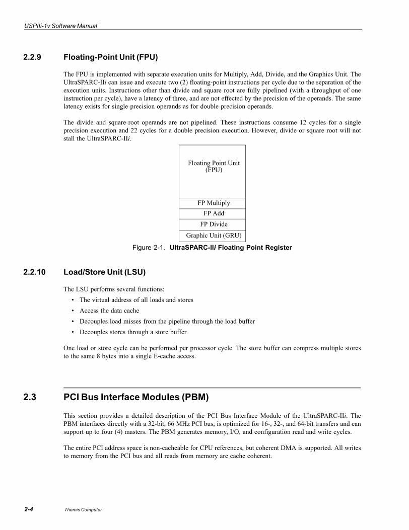
2.2.9 Floating-Point Unit (FPU)
The FPU is implemented with separate execution units for Multiply, Add, Divide, and the Graphics Unit. TheUltraSPARC-IIi can issue and execute two (2) floating-point instructions per cycle due to the separation of theexecution units. Instructions other than divide and square root are fully pipelined (with a throughput of oneinstruction per cycle), have a latency of three, and are not effected by the precision of the operands. The samelatency exists for single-precision operands as for double-precision operands.
The divide and square-root operands are not pipelined. These instructions consume 12 cycles for a singleprecision execution and 22 cycles for a double precision execution. However, divide or square root will notstall the UltraSPARC-IIi.
Figure 2-1. UltraSPARC-IIi Floating Point Register
2.2.10 Load/Store Unit (LSU)
The LSU performs several functions:• The virtual address of all loads and stores • Access the data cache • Decouples load misses from the pipeline through the load buffer• Decouples stores through a store buffer
One load or store cycle can be performed per processor cycle. The store buffer can compress multiple storesto the same 8 bytes into a single E-cache access.
2.3 PCI Bus Interface Modules (PBM)
This section provides a detailed description of the PCI Bus Interface Module of the UltraSPARC-IIi. ThePBM interfaces directly with a 32-bit, 66 MHz PCI bus, is optimized for 16-, 32-, and 64-bit transfers and cansupport up to four (4) masters. The PBM generates memory, I/O, and configuration read and write cycles.
The entire PCI address space is non-cacheable for CPU references, but coherent DMA is supported. All writesto memory from the PCI bus and all reads from memory are cache coherent.
FP MultiplyFP Add
FP Divide
Graphic Unit (GRU)
Floating Point Unit(FPU)
2-4 Themis Computer

2. UltraSPARC-IIi CPU Description
2.3.1 Unsupported PCI Features
There are several PCI features that are not supported by the UltraSPARC-IIi. These features are:• Exclusive Access to main memory (Memory LOCK)• Peer-to-peer transfers between bus segments• Cache support• Cache-line Wrap Addressing Mode• Fast Back-to-Back cycles as a PIO master• Address/Data Stepping• Subtractive decode• All DOS compatibility features
2.3.2 PCI Bus Operations
2.3.2.1 Transaction Termination• Retries: The maximum number of retries is referred to as the Retry Limit Count and is fixed at 512.
When the number of retries exceeds the Retry Limit Count the PBM ceases to attempt the transactionand issues an interrupt to the processor.
• Disconnects: A disconnect occurs when a transaction is halted. No count of disconnects is maintained.The transaction is restarted with the next data to be transferred.
• Master-Abort: A Master-Abort typically occurs when no device responds to the PIO address and theMaster aborts the transaction.
• Target-Abort: A Target-Abort is an abort issued by the target device. A target abort may be caused by avariety of error conditions. For more information, refer to the Chapter 16, “Error Handling,” of theUltraSPARC-IIi User’s Manual.
2.3.3 Read/Write Cycles
Read and Write cycles as described in the PCI Specification, Version 2.1, are supported.
The UltraSPARC-IIi will normally generate a disconnect when a DMA burst transfer passes a line (64 Bytes)boundary. The master device will restart the transaction at the address of the next data to be transferred.
The UltraSPARC-IIi is capable of generating arbitrary byte enables on PIO writes. It is also capable ofgenerating aligned PIO reads of 1, 2, 4, 8, 16, and 64 bytes. A target device is required to drive all data byteson reads, but is not required to support arbitrary byte enables on writes. The target device may terminate thecycle with a target-abort if an illegal byte enable combination is signalled. The UltraSPARC-IIi supportsarbitrary byte enables for all DMA transactions.
Themis Computer 2-5
USPIIi-1v Software Manual
2.3.4 Endian-ness
A big-endian address is an address for which the address of a half-word, word, doubleword or quadword isthe address of its most significant byte. A little-endian address is an address for which the address of a half-word, word, doubleword or quadword is the address of the least significant byte. For a more completedefinition of endian-ness, refer to Section 6.3.1.2, “Addressing Conventions,” in The SPARC ArchitectureManual, Version 9.
The internal architecture, UPA64S, and DRAM system interfaces of the UltraSPARC-IIi are big-endian. ThePCI bus is little-endian. To route the byte lanes of the UltraSPARC-IIi correctly, the internal data busses ofthe UltraSPARC-IIi are connected to the PCI bus in a ‘byte-twisted’ fashion. Data bits [63:56] of theUltraSPARC-IIi are connected to PCI data bits [7:0]. Data bits [55:48] of the UltraSPARC-IIi are connectedto PCI data bits [15:8], and so on. The PBM internal control registers, which are big-endian, are byte-twistedagain.
This implementation allows all byte sized PIOs and byte-stream DMA to be handled correctly.
2.3.4.1 Big-endian and Little- endian Address Space
The UltraSPARC-IIi’s 8 GB address space is separated into several different regions. The lower 16 MB, from0x1FE.0000.0000 to 0x1FE.00FF.FFFF, allows access to internal registers with the UltraSPARC-IIi I/O. Thisportion is big-endian and there is no byte twisting done for accesses in this region.
The address space from 0x1FE.0202.0000 to 0x1FE.FFFF.FFFF is unused/reserved. Writes to this region areignored and reads return 0.
All remaining regions are little-endian. The 4GB region from 0x1FF.0000.0000 to 0x1FF.FFFF.FFFF is toaccess the PCI memory space. The 16 MB region from 0x0.0100.000 to 0x0.01FF.FFFF is used to access thePCI configuration space. There are two (2) 64 KB regions from 0x0200.0000 to 0x02FF.FFFF that are used toaccess PCI bus I/O space. All access to these areas are little-endian and use byte-twisting.
Note — Any configuration and status register in the APB ASIC on the UltraSPARC-IIi must be accessedwith little-endian loads and stores, or the access will appear byte-twisted. However, all configuration andstatus registers within the UltraSPARC-IIi must be accessed with big-endian loads and stores except forthose used to access the PCI configuration space.
For more information on the big- and little-endian support provided in the UltraSPARC-IIi, refer to Section9.4, “Little-endian Support,” of the UltraSPARC-IIi Hardware Manual.
2.4 Memory Management Units (MMU)
There are two separate Memory Management Units present in the UltraSPARC-IIi: the Instruction MMU andthe Data MMU. Collectively these units are referred to as the MMU. The UltraSPARC-IIi MMU conforms tothe requirements set forth for a SPARC-V9 System.
2-6 Themis Computer
2. UltraSPARC-IIi CPU Description
Note — The UltraSPARC-IIi MMU does not conform to the SPARC-V8 specification. The UltraSPARC-IIi MMU supports a 44-bit virtual address space, software (only) TLB miss processing (with no hardwaretable walk), simplified protection encoding, and multiple page sizes. These features are not supported in theSPARC-V8 specification.
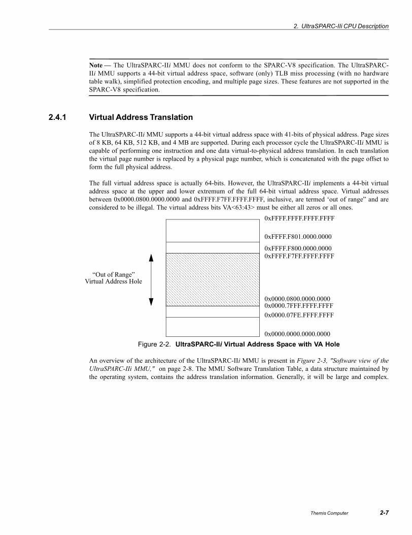
2.4.1 Virtual Address Translation
The UltraSPARC-IIi MMU supports a 44-bit virtual address space with 41-bits of physical address. Page sizesof 8 KB, 64 KB, 512 KB, and 4 MB are supported. During each processor cycle the UltraSPARC-IIi MMU iscapable of performing one instruction and one data virtual-to-physical address translation. In each translationthe virtual page number is replaced by a physical page number, which is concatenated with the page offset toform the full physical address.
The full virtual address space is actually 64-bits. However, the UltraSPARC-IIi implements a 44-bit virtualaddress space at the upper and lower extremum of the full 64-bit virtual address space. Virtual addressesbetween 0x0000.0800.0000.0000 and 0xFFFF.F7FF.FFFF.FFFF, inclusive, are termed ‘out of range” and areconsidered to be illegal. The virtual address bits VA<63:43> must be either all zeros or all ones.
Figure 2-2. UltraSPARC-IIi Virtual Address Space with VA Hole
An overview of the architecture of the UltraSPARC-IIi MMU is present in Figure 2-3, "Software view of theUltraSPARC-IIi MMU," on page 2-8. The MMU Software Translation Table, a data structure maintained bythe operating system, contains the address translation information. Generally, it will be large and complex.
0xFFFF.FFFF.FFFF.FFFF
0xFFFF.F801.0000.0000
0xFFFF.F800.0000.00000xFFFF.F7FF.FFFF.FFFF
0x0000.0800.0000.00000x0000.7FFF.FFFF.FFFF0x0000.07FE.FFFF.FFFF
0x0000.0000.0000.0000
“Out of Range”Virtual Address Hole
Themis Computer 2-7

USPIIi-1v Software Manual
The MMU Translation Look-aside Buffers, implemented in the MMU hardware, act as independent buffersfor the MMU Software Translation Table. They are small and fast. The MMU Translation Storage Buffer(TSB) acts as an interface between the MMU TLBs and the MMU Software Translation Table.
Figure 2-3. Software view of the UltraSPARC-IIi MMU
2.5 I/O Memory Management Unit (IOM)
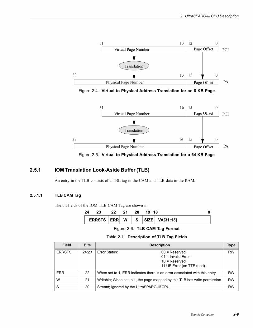
When DVMA read/write access is required, the IOM performs address translations from 32-bit DVMA to 34-bit physical addresses when the UltraSPARC-IIi is a PCI target.
To facilitate address translations, the UltraSPARC-IIi IOM contains 16-entry, fully associative data andTranslation Lookaside Buffers (TLBs) and a one-level, software managed data structure referred to as theTranslation Storage Buffer (TSB). Although the IOM TSB and the IOM TLB are entirely separate from theMMU TLB and the MMU TSB, even though they perform similar functions. In this section all reference tothe TLB and the TSB refer to the IOM TLB and the IOM TSB, unless otherwise noted. The IOM TLBs storerecently used translations and the IOM TSB maintains the address translation information for the USPIIi-1v.When a translations can not be found in the IOM TLB, UltraSPARC-IIi hardware performs a IOM TSBlookup (also known as a hardware table walk). If the IOM TSB lookup fails to return a valid mapping, theIOM returns an error to the PCI master device attempting the access.
There are three types of operational DMA IOM modes: translation, bypass, and pass-through. In thetranslation mode the PBM initiates a translation by providing a 32-bit virtual address. The IOM hardwareperforms a lookup in the IOM TLB. If the lookup results in a TLB hit, the IOM translates the address andreturns the 34-bit virtual address. If a TLB miss occurs, a TSB lookup is automatically initiated by hardware.If a TSB hit occurs, the information is loaded into the TLB and the translation continues. If a TSB missoccurs, the IOM returns an error to the PBM. Figure 2-4 Virtual to Physical Address Translation for an 8 KBPage on page 2-9 and Figure 2-5, "Virtual to Physical Address Translation for a 64 KB Page," on page 2-9illustrate a translation mode operation.
In the bypass mode, the IOM allows a PCI device to have direct, un-restricted access to the entire physicalmemory. The PCI device is assumed to support its own MMU and bypasses the IOM. In this mode, thephysical address is equivalent to the PCI Address and no translation, apart from what is done internal to thePCI device, is necessary or performed.
The pass-through mode allows access to the main memory (DRAM) only. In the pass-through mode the upperbits of the physical address are padded with 0.
O/S Data StructureMemoryMMU
TranslationLookaside
Buffer
Translation Storage Buffer
SoftwareTranslation
Table(TLB) (TSB)
2-8 Themis Computer
2. UltraSPARC-IIi CPU Description
Figure 2-4. Virtual to Physical Address Translation for an 8 KB Page
Figure 2-5. Virtual to Physical Address Translation for a 64 KB Page
2.5.1 IOM Translation Look-Aside Buffer (TLB)
An entry in the TLB consists of a TBL tag in the CAM and TLB data in the RAM.
2.5.1.1 TLB CAM Tag
The bit fields of the IOM TLB CAM Tag are shown in
Figure 2-6. TLB CAM Tag Format
Table 2-1. Description of TLB Tag Fields
Field Bits Description Type
ERRSTS 24:23 Error Status: 00 = Reserved01 = Invalid Error10 = Reserved11 UE Error (on TTE read)
RW
ERR 22 When set to 1, ERR indicates there is an error associated with this entry. RW
W 21 Writable; When set to 1, the page mapped by this TLB has write permission. RW
S 20 Stream; Ignored by the UltraSPARC-IIi CPU. RW
PCI
PA01213
0121331
33
Translation
Page Offset
Page Offset
Virtual Page Number
Physical Page Number
PCI
PA01516
0151631
33
Translation
Page Offset
Page Offset
Virtual Page Number
Physical Page Number
VA[31:13]SIZESWERRERRSTS
018192021222324
Themis Computer 2-9
USPIIi-1v Software Manual
2.5.1.2 TLB RAM Data
The bit fields of the IOM TLB CAM Tag are shown in Table 2-7, "TLB RAM DATA Format."
Figure 2-7. TLB RAM DATA Format
2.5.2 IOM Translation Storage Buffer
The IOM Translation Storage Buffer (TSB) is a one-level, software maintained, data structure held inmemory. It provides virtual to physical address translation information. When a translation can not be locatedin the TLB, the IOM hardware looks up the TSB to provide the translation information. An entry in theTranslation Storage Table is referred to as a Translation Table Entry (TTE). A TTE is eight bytes long.
SIZE 19 0 mean 8K page; 1 mean a 64K page. RW
VA [31:13] 18:0 19-bit Virtual Page Number RW
Table 2-2. Description of TLB RAM Data Fields
Field Bits Description Type
V 30 Valid bit; When set, the TLB data filed is meaningful RW
U 29 Used bit; affects the LRU replacement. RW
C 28 Cacheable bit: 0 = Non-Cacheable Access1 = Cacheable Access
RW
PA[40:34] 27:21 Not Stored; all ‘1’s if Non-Cacheable Access, all ‘0’s is cacheable access RW
PA[33:13] 20:0 21-bit physical page number RW
Table 2-3. TTE Formata
Field Bits Description
DATA_v 63 Valid bit (1 = TTE entry has valid mapping.)
DATA_SIZE 61 Page size of the mapping (0 = 8K; 1 = 64K)
STREAM 60 Stream Bit 0 = Consistent Page1 = Streamable Page
LOCALBUS 59 Local Bus Bit; not used
DATA_SOFT_2 58:51 Reserved for Software Use
DATA_PA 40:13 Contains bits [33:13] of physical address; bits [15:13] are not used for 64K pages; bits [40:34] are not used and implied to be 1 if non-cacheable, 0 if cacheable.
DATA_SOFT 12:7 Reserved for software use.
Table 2-1. Description of TLB Tag Fields
Field Bits Description Type
PA[33:13]‘0’s or ‘1’sCUV
02027:21282930
2-10 Themis Computer
2. UltraSPARC-IIi CPU Description
2.5.2.1 Translation Errors
The translation errors detected by the IOM are:
Invalid Errors: An invalid error happens if bit DATA_V in the TTE read by the IOM hardware indicates thatthe TTE is invalid (DATA_V = 0).
Protection Error: A protection error is detected if the PCI device performs a DMA write to a read-only page.
TTE UE Error: If a correctable ECC error occurred during access to the TSB, the MCU will correct the errorand the TTE received is error free. If an uncorrectable ECC occurred, the TTE will be invalid and the IOMwill flag the error.
2.6 Instruction and Data Cache
2.6.1 I-Cache
The I-Cache is 16 KB two-way set-associative cache with 32-byte blocks. The I-Cache is physically indexedand physically tagged. The set is predicted as part of the “next field” (on the basis of the next fetch address)so that only the index bits of an address are necessary to address the cache. This implies that only the lowest13 bits, which matches the minimum page size of 8 KB are necessary to index into the I-Cache. The resultingtag is compared against the translated physical address to determine I-Cache hits. The I-Cache can return upto four (4) instructions per access from a line that is eight (8) instructions wide.
The instruction fetches may bypass the I-Cache when any of the following conditions are true: • the I-Cache enable or I-MMU enable bits in the LSU_Control_Register are clear (refer to Table 2-4,
"LSU_Control_Register," on page 2-12)• the UltraSPARC-IIi is in the RED_state• the iTLB maps the fetch as non-cacheable
Note — The size of each I-Cache set is the same as the page size in the UltraSPARC-IIi. Thus, the virtualindex bits equals the physical index bits.
CACHEABLE 4 Cacheable 0 = Non-Cacheable Page1 = Cacheable Page
DATA_W 1 Set if page is writable.
a. All bits not mentioned in this table are “Reserved” for use by the UltraSPARC-IIi.
Table 2-3. TTE Formata
Field Bits Description
Themis Computer 2-11

USPIIi-1v Software Manual
The I-Cache snoops the store from DMA transfers, but is not updated unless the store is a block commit store.Block commit stores invalidate the I-Cache but do not flush instructions that have been prefetched into thepipeline. A FLUSH, DONE, or RETRY instruction can be used to flush the pipeline.
2.6.2 D-Cache
The D-Cache is a write-through, non-allocating-on-write-miss, 16 KB direct-mapped cache with two 16-bytesub-blocks per line. The D-Cache is virtually indexed and physically tagged. Virtual addresses are used toindex into the D-cache tag and data arrays while accessing the TLB. The resulting tag is compared against thetranslated physical address to determine the D-Cache hits. The tag updates are dual ported so that the tagupdates do not collide with tag reads for incoming loads. Snoops to the D-Cache use the second tag port sothat an incoming load can proceed without interruption by a snoop.
In a similar manner to data accesses to the I-Cache, data accesses bypass the D-Cache when the D-Cacheenable bit is the LSU_Control_Register (Refer to Table 2-4, "LSU_Control_Register," on page 2-12) is clear.Load misses will not allocate in the D-Cache if the D-MMU bit in the LSU_Control_Register is clear or theaccess is mapped by the iTLB as non-cacheable.
Note — Software must flush the D-Cache when changing a physical page from cacheable to non-cacheableor when an illegal address alias is created through the virtually indexed cache. In order to flush the cache,software must read a range of read-only addresses that map to the corresponding cache line being flushed.The read will force any modified entries in the local cache out. Care must be taken to ensure that the rangeof the read-only addresses is mapped in the MMU before starting a displacement flush, otherwise the TLBmiss handler may put new data into the caches.
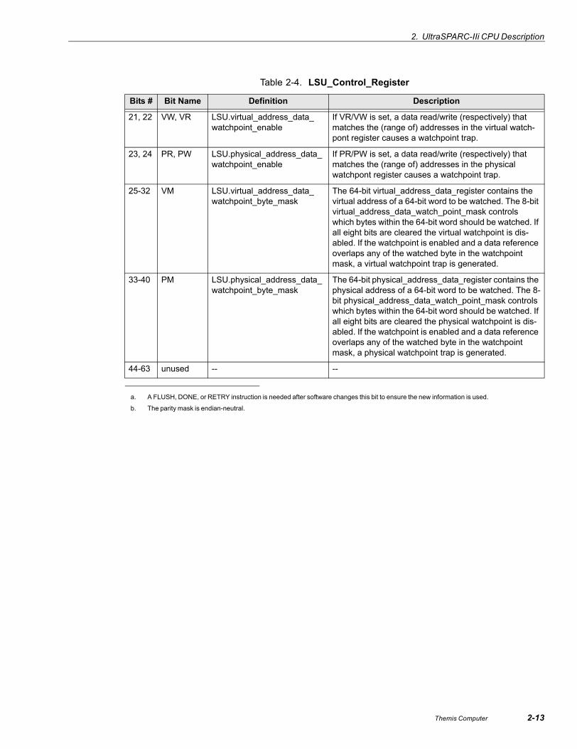
2.6.3 LSU_Control_Register
The LSU_Control_Register contains fields that control the hardware functions of the I-Cache, D-Cache,MMU (TLBs), bad parity generation, and watchpoint settings. The definition of the LSU_Control_Register isprovided below Table 2-4, "LSU_Control_Register."
Table 2-4. LSU_Control_Register
Bits # Bit Name Definition Description
0 IC LSU.I-cache_enable If cleared misses are forced on I-Cache accesses with no cache fill.
1 CD LSU.D-cache_enablea If cleared misses are forced on D-cache accesses with no cache fill.
2 IM LSU.enable_I-MMU If cleared, the I-MMU (iTLB) is disabled (pass-through mode).
3 DM LSU.endable_D-MMU If cleared, the D-MMU (dTLB) is disabled (pass-through mode).
4-19 FM<15:0> LSU.parity_maskb The UltraSPARC-IIi write generates incorrect parity on the E-cache data bus for bytes to the 16 bytes of the E-cache data bus.
20 Unused -- --
2-12 Themis Computer
2. UltraSPARC-IIi CPU Description
21, 22 VW, VR LSU.virtual_address_data_watchpoint_enable
If VR/VW is set, a data read/write (respectively) that matches the (range of) addresses in the virtual watch-pont register causes a watchpoint trap.
23, 24 PR, PW LSU.physical_address_data_watchpoint_enable
If PR/PW is set, a data read/write (respectively) that matches the (range of) addresses in the physical watchpont register causes a watchpoint trap.
25-32 VM LSU.virtual_address_data_watchpoint_byte_mask
The 64-bit virtual_address_data_register contains the virtual address of a 64-bit word to be watched. The 8-bit virtual_address_data_watch_point_mask controls which bytes within the 64-bit word should be watched. If all eight bits are cleared the virtual watchpoint is dis-abled. If the watchpoint is enabled and a data reference overlaps any of the watched byte in the watchpoint mask, a virtual watchpoint trap is generated.
33-40 PM LSU.physical_address_data_watchpoint_byte_mask
The 64-bit physical_address_data_register contains the physical address of a 64-bit word to be watched. The 8-bit physical_address_data_watch_point_mask controls which bytes within the 64-bit word should be watched. If all eight bits are cleared the physical watchpoint is dis-abled. If the watchpoint is enabled and a data reference overlaps any of the watched byte in the watchpoint mask, a physical watchpoint trap is generated.
44-63 unused -- --
a. A FLUSH, DONE, or RETRY instruction is needed after software changes this bit to ensure the new information is used.
b. The parity mask is endian-neutral.
Table 2-4. LSU_Control_Register
Bits # Bit Name Definition Description
Themis Computer 2-13

USPIIi-1v Software Manual
2-14 Themis Computer

Themis Computer 3-1
3
3Themis USPIIi-1V address Map
3.1 Introduction
This chapter provides detailed descriptions of the address maps and register address locations for the ThemisUSPIIi-1v VME board.
3.2 USPIIi-1V Address Map
The UltraSPARC-IIi CPU used on the Themis USPIIi-1v VME board divides its physical address spaceamong:
• DRAM
• UPA64S (In the case where a FFB (Creator Graphics) graphic device is used)
• PCI, that is further subdivided into PCI A and B bus spaces by the Advanced PCI Bridge (APB).
Table 3-1. UltraSPARC-IIi Address Map
Address Range in PA <40:0> Size Port Addressed
Access type
0x000.0000.0000-0x000.3FFFF.FFFF
1 GB Main Memory Cacheable
0x000.4000.0000-0x1FF.0000.0000
Do not use Undefined Cacheable
0x000.0000.0000-0x1FB.0000.0000
Do not use Undefined Non Cacheable
0x1FC.0000.0000-0x1FD.FFFF.FFFF
8 GB UPA64S (FFB) Non Cacheable
0x1FE.0000.0000-0x1FF.FFFF.FFFF
8 GB PCI Non Cacheable
USPIIi-1v Software Manual
3-2 Themis Computer
3.3 PCI Address Map
The UltraSPARC-IIi CPU directly interfaces to the PCI bus, through the PBM (PCI Bus Module). Here is thePCI Bus mapping as seen from the CPU:
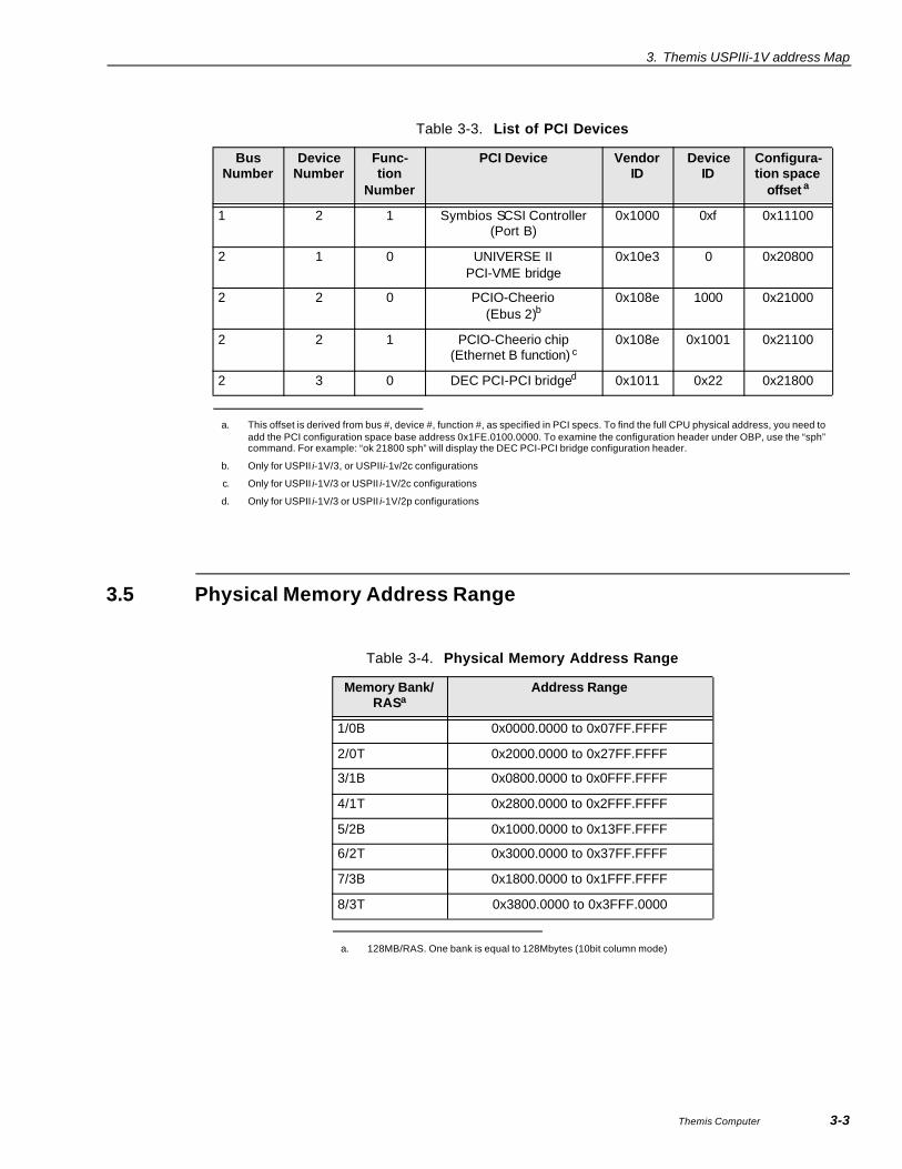
3.4 List of PCI devices
This table lists all on-board PCI devices that are attached to the PCI Bus interface. This doesn’t include thePMC expansion cards that may be plugged on the USPII i-1v/2p and USPIIi-1v/3 PMC expansion.
Table 3-2. Physical address space to PCI space
PCI Address Space PA[40:0] CPU CommandsSupported
PCI Commands Gen-erated
PCI ConfigurationSpace
0x1FE.0100.0000-0x1FE.01FF.FFFF
Non Cacheable read (any)Non Cacheable write (any)
Configuration ReadConfiguration Write(may also be SpecialCycle)
PCI Bus I/O Space 0x1FE.0200.0000-0x1FE.02FF.FFFF
NC read (any)NC write (any)
I/O ReadI/O Write
Don’t Use 0x1FE.0300.0000-0x1FE.FFFF.FFFF
-- May wrap toConfiguration or I/OSpace behavior
PCI Bus MemorySpace
0x1FF.0000.0000-0x1FF.FFFF.FFFF
NC read (4 byte)NC read (8 byte)NC Block readNC writeNC Block writeNC Instruction fetch
Memory ReadMemory Read MultipleMemory Read LineMemory WriteMemory WriteMemory Read
Table 3-3. List of PCI Devices
Bus Number
Device Number
Func-tion
Number
PCI Device Vendor ID
Device ID
Configura-tion space
offseta
0 0 0 CPU PCI Bus Module 0x108e 0xa000 0
0 1 0 APB chip (Bus A) 0x108e 0x5000 0x800
0 1 1 APB chip (Bus B) 0x108e 0x5000 0x900
1 1 0 PCIO-Cheerio (Ebus 1)
0x108e 0x1000 0x10800
1 1 1 PCIO-Cheerio (Ethernet A)
0x108e 0x1001 0x10900
1 2 0 Symbios SCSI Controller (Port A)
0x1000 0xf 0x11000
Themis Computer 3-3
3. Themis USPIIi-1V address Map
3.5 Physical Memory Address Range
1 2 1 Symbios SCSI Controller (Port B)
0x1000 0xf 0x11100
2 1 0 UNIVERSE II PCI-VME bridge
0x10e3 0 0x20800
2 2 0 PCIO-Cheerio (Ebus 2)b
0x108e 1000 0x21000
2 2 1 PCIO-Cheerio chip (Ethernet B function) c
0x108e 0x1001 0x21100
2 3 0 DEC PCI-PCI bridged 0x1011 0x22 0x21800
a. This offset is derived from bus #, device #, function #, as specified in PCI specs. To find the full CPU physical address, you need to add the PCI configuration space base address 0x1FE.0100.0000. To examine the configuration header under OBP, use the “sph” command. For example: “ok 21800 sph” will display the DEC PCI-PCI bridge configuration header.
b. Only for USPII i-1V/3, or USPIIi-1v/2c configurations
c. Only for USPII i-1V/3 or USPII i-1V/2c configurations
d. Only for USPII i-1V/3 or USPII i-1V/2p configurations
Table 3-4. Physical Memory Address Range
Memory Bank/RASa
a. 128MB/RAS. One bank is equal to 128Mbytes (10bit column mode)
Address Range
1/0B 0x0000.0000 to 0x07FF.FFFF
2/0T 0x2000.0000 to 0x27FF.FFFF
3/1B 0x0800.0000 to 0x0FFF.FFFF
4/1T 0x2800.0000 to 0x2FFF.FFFF
5/2B 0x1000.0000 to 0x13FF.FFFF
6/2T 0x3000.0000 to 0x37FF.FFFF
7/3B 0x1800.0000 to 0x1FFF.FFFF
8/3T 0x3800.0000 to 0x3FFF.0000
Table 3-3. List of PCI Devices
Bus Number
Device Number
Func-tion
Number
PCI Device Vendor ID
Device ID
Configura-tion space
offset a
USPIIi-1v Software Manual
3-4 Themis Computer
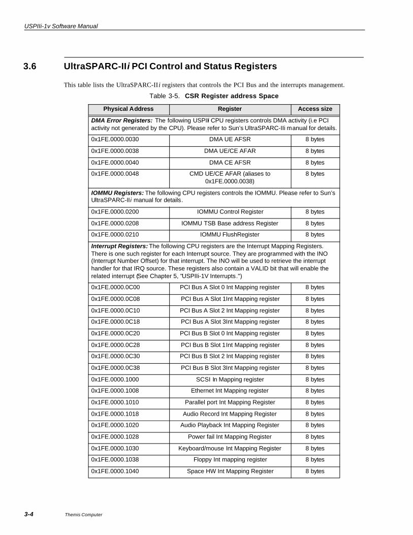
3.6 UltraSPARC-IIi PCI Control and Status Registers
This table lists the UltraSPARC-II i registers that controls the PCI Bus and the interrupts management.
Table 3-5. CSR Register address Space
Physical Address Register Access size
DMA Error Registers: The following USPIIi CPU registers controls DMA activity (i.e PCI activity not generated by the CPU). Please refer to Sun’s UltraSPARC-IIi manual for details.
0x1FE.0000.0030 DMA UE AFSR 8 bytes
0x1FE.0000.0038 DMA UE/CE AFAR 8 bytes
0x1FE.0000.0040 DMA CE AFSR 8 bytes
0x1FE.0000.0048 CMD UE/CE AFAR (aliases to 0x1FE.0000.0038)
8 bytes
IOMMU Registers: The following CPU registers controls the IOMMU. Please refer to Sun’s UltraSPARC-IIi manual for details.
0x1FE.0000.0200 IOMMU Control Register 8 bytes
0x1FE.0000.0208 IOMMU TSB Base address Register 8 bytes
0x1FE.0000.0210 IOMMU FlushRegister 8 bytes
Interrupt Registers: The following CPU registers are the Interrupt Mapping Registers. There is one such register for each Interrupt source. They are programmed with the INO (Interrupt Number Offset) for that interrupt. The INO will be used to retrieve the interrupt handler for that IRQ source. These registers also contain a VALID bit that will enable the related interrupt (See Chapter 5, "USPIIi-1V Interrupts.")
0x1FE.0000.0C00 PCI Bus A Slot 0 Int Mapping register 8 bytes
0x1FE.0000.0C08 PCI Bus A Slot 1Int Mapping register 8 bytes
0x1FE.0000.0C10 PCI Bus A Slot 2 Int Mapping register 8 bytes
0x1FE.0000.0C18 PCI Bus A Slot 3Int Mapping register 8 bytes
0x1FE.0000.0C20 PCI Bus B Slot 0 Int Mapping register 8 bytes
0x1FE.0000.0C28 PCI Bus B Slot 1Int Mapping register 8 bytes
0x1FE.0000.0C30 PCI Bus B Slot 2 Int Mapping register 8 bytes
0x1FE.0000.0C38 PCI Bus B Slot 3Int Mapping register 8 bytes
0x1FE.0000.1000 SCSI In Mapping register 8 bytes
0x1FE.0000.1008 Ethernet Int Mapping register 8 bytes
0x1FE.0000.1010 Parallel port Int Mapping Register 8 bytes
0x1FE.0000.1018 Audio Record Int Mapping Register 8 bytes
0x1FE.0000.1020 Audio Playback Int Mapping Register 8 bytes
0x1FE.0000.1028 Power fail Int Mapping Register 8 bytes
0x1FE.0000.1030 Keyboard/mouse Int Mapping Register 8 bytes
0x1FE.0000.1038 Floppy Int mapping register 8 bytes
0x1FE.0000.1040 Space HW Int Mapping Register 8 bytes

Themis Computer 3-5
3. Themis USPIIi-1V address Map
0x1FE.0000.1048 Keyboard Int Mapping register 8 bytes
0x1FE.0000.1050 Mouse Int mapping Register 8 bytes
0x1FE.0000.1058 Serial Int Mapping Register 8 bytes
0x1FE.0000.1070 DMA UE Int Mapping Register 8 bytes
0x1FE.0000.1078 DMA CE Int Mapping Register 8 bytes
0x1FE.0000.1080 PCI Error Int Mapping Register 8 bytes
0x1FE.0000.1098 On Board Graphic Int Mapping Register (also mapped at 0x1FE.0000.6000)
8 bytes
0x1FE.0000.10A0 Expansion UPA64 Int mapping register
Interrupt clear registers:
0x1FE.0000.1400 to0x1FE.0000.1418
PCI bus A slot 0 clear Int registers 8 bytes
0x1FE.0000.1420 to 0x1FE.0000.1438
PCI Bus A slot 1 clear registers 8 bytes
0x1FE.0000.1440 to0x1FE.0000.1458
PCI Bus A slot 2 clear Int registers 8 bytes
0x1FE.000.1460 to0x1FE.0000.1478
PCI Bus A slot 3 clear Int register 8 bytes
0x1FE.0000.1480 to0x1FE.0000.1498
PCI bus B slot 0 clear Int registers 8 bytes
0x1FE.0000.14A0 to0x1FE.0000.14B8
PCI Bus B slot 1 clear registers 8 bytes
0x1FE.0000.14C0 to0x1FE.0000.14D8
PCI Bus B slot 2 clear Int registers 8 bytes
0x1FE.0000.14E0 to0x1FE.0000.14D8
PCI Bus B slot 3 clear Int register 8 bytes
0x1FE.0000.0180 SCSI clear Int register 8 bytes
0x1FE.0000.1808 Ethernet clear Int register 8 bytes
0x1FE.0000.1810 Parallel port clear Int register 8 bytes
0x1FE.0000.1818 Audio record clear Int register 8 bytes
0x1FE.0000.1820 Audio Playback clear Int register 8 bytes
0x1FE.0000.1828 Power fail clear Int register 8 bytes
0x1FE.0000.1830 Keyboard / mouse clear Int register 8 bytes
0x1FE.0000.1838 Floppy clear Int register 8 bytes
0x1FE.0000.1840 Spare HW clear Int register 8 bytes
0x1FE.0000.1848 Keyboard clear Int register 8 bytes
0x1FE.0000.1858 Serial clear Int register 8 bytes
0x1FE.0000.1870 DMA UE clear Int register 8 bytes
Table 3-5. CSR Register address Space
Physical Address Register Access size

USPIIi-1v Software Manual
3-6 Themis Computer
0x1FE.0000.1878 DMA CE clear Int register 8 bytes
0x1FE.0000.1880 PCI error clear Int register 8 bytes
0x1FE.0000.1C20 PCI DMA write synchronization register 8 bytes
0x1FE.0000.2000 PCI control / status register 8 bytes
0x1FE.0000.2010 PCI PIO write AFSR 8 bytes
0x1FE.0000.2018 PCI PIO write AFAR 8 bytes
0x1FE.0000.2020 PCI diagnostic register 8 bytes
0x1FE.0000.2028 PCI target address space register 8 bytes
0x1FE.0000.5000 to0x1FE.0000.5038
PCI buffer diag access 8 bytes
0x1FE.0000.5100 to0x1FE.0000.5138
DMA buffer diag access 8 bytes
0x1FE.0000.51C0 DMA buffer diag access (72:64) 8 bytes
0x1FE.0000.6000 On-board graphics Int Mapping register (also mapped at 0x1FE.0000.1098)
8 bytes
0x1FE.0000.8000 Expansion UPA64S Int mapping register (also mapped at 0x1FE.0000.10A0)
8 bytes
0x1FE.0000.A400 IOMMU virtual address diag register 8 bytes
0x1FE.0000.A408 IOMMU tag compare diag 8 bytes
0x1FE.0000.A580 to0x1FE.0000.A5FF
IOMMU tag details 8 bytes
0x1FE.0000.A600 to0x1FE.0000.A67F
IOMMU data RAM diag 8 bytes
0x1FE.0000.A800 PCI Int state diag register 8 bytes
0x1FE.0000.A808 OBIO and misc Int State diag register 8 bytes
0x1FE.0000.F010 MC_Control0 4 bytes
0x1FE.0000.F018 MC_Control1 4 bytes
0x1FE.0000.F020 Reset _Control 4 bytes
0x1FE.0200.0000 to0x1FE.02FF.FFFF
PCI Bus I/O bus -2 byte
0x1FF.0000.0000 to0x1FF.FFFF.FFFF
PCI bus memory space 3 bytes
PCI Bus Module (PBM) registers: The following CPU registers control aspects of USPIIi’s PCI operations that are not defined by the PCI specification. The registers defined by the PCI specification are listed in the following section ( PBM Configuration space registers)
0x1FE.0000.2000 PCI Control / Status Register 8 bytes
0x1FE.0000.2010 PCI PIO Write AFSR 8 bytes
0x1FE.0000.2018 PCI PIO Write AFAR 8 bytes
Table 3-5. CSR Register address Space
Physical Address Register Access size

Themis Computer 3-7
3. Themis USPIIi-1V address Map
3.7 Advanced PCI Bridge (APB) configuration space registers
The ABP is connected to the UltraSPARC-II i PBM interface and splits the PCI into two PCI buses, A and B.
The APB internal configuration space is organized as 2 functions. Function 0 contains registers fortransactions to/from PCI Bus A. Function 1 contains registers for transactions to/from PCI bus B. The APBIDSEL pin is connected to Bus 0 AD[12] signal. This means APB is device 1 on PCI bus 0. APB registers canbe divided into two classes:
0x1FE.0000.2020 PCI Diagnostic Register 8 bytes
0x1FE.0000.2028 PCI Target Address Space Register 8 bytes
0x1FE.0000.1C20 PCI DMA Write Synchronization Register 8 bytes
0x1FE.0000.5000 to0x1FE.0000.5038
PIO Data Buffer Diagnostics Access 8 bytes
0x1FE.0000.5100 to0x1FE.0000.5138
DMA Data Buffer Diagnostics Access 8 bytes
0x1FE.0000.51C0 DMA Data Buffer Diagnostics Access (72:64)
8 bytes
PBM Configuration Space registers: The PBM contains a configuration header whose for-mat is specified by the PCI specification. The registers in the PBM configuration header are accessed through PCI configuration address space. The PBM is considered to be device 0 and function 0 on bus 0. This means that the configuration header base address will be 0x1FE.0100.000. Also note that the PCI configuration space is little endian.
0x1FE.0100.0000 Vendor ID (0x108E) 2 bytes
0x1FE.0100.0002 Device ID (0xA000) 2 bytes
0x1FE.0100.0004 Command register 2 bytes
0x1FE.0100.0006 Status register 2 bytes
0x1FE.0100.0008 Revision ID 1 bytes
0x1FE.0100.0009 Programming I/F code 1 byte
0x1FE.0100.000A Sub-class Code 1 byte
0x1FE.0100.000B Base class code 1 byte
0x1FE.0100.000D Latency time register 1 byte
0x1FE.0100.000E Header type 1 byte
(The two following registers are part of the PCI optional bridge configuration header, as the PBM is considered to be a PCI bridge device).)
0x1FE.0100.0040 Bus Number 1 byte
0x1FE.0100.0041 Subordinate bus 1 byte
Table 3-5. CSR Register address Space
Physical Address Register Access size
USPIIi-1v Software Manual
3-8 Themis Computer
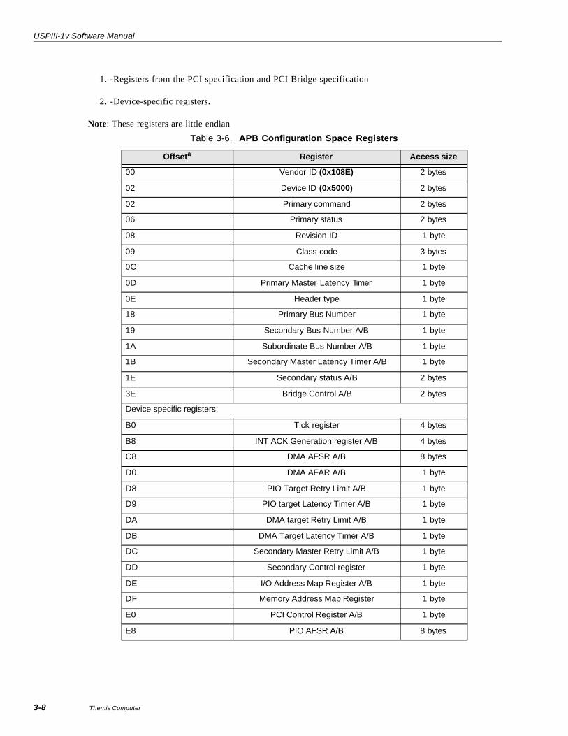
1. -Registers from the PCI specification and PCI Bridge specification
2. -Device-specific registers.
Note: These registers are little endian
Table 3-6. APB Configuration Space Registers
Offseta Register Access size
00 Vendor ID (0x108E) 2 bytes
02 Device ID (0x5000) 2 bytes
02 Primary command 2 bytes
06 Primary status 2 bytes
08 Revision ID 1 byte
09 Class code 3 bytes
0C Cache line size 1 byte
0D Primary Master Latency Timer 1 byte
0E Header type 1 byte
18 Primary Bus Number 1 byte
19 Secondary Bus Number A/B 1 byte
1A Subordinate Bus Number A/B 1 byte
1B Secondary Master Latency Timer A/B 1 byte
1E Secondary status A/B 2 bytes
3E Bridge Control A/B 2 bytes
Device specific registers:
B0 Tick register 4 bytes
B8 INT ACK Generation register A/B 4 bytes
C8 DMA AFSR A/B 8 bytes
D0 DMA AFAR A/B 1 byte
D8 PIO Target Retry Limit A/B 1 byte
D9 PIO target Latency Timer A/B 1 byte
DA DMA target Retry Limit A/B 1 byte
DB DMA Target Latency Timer A/B 1 byte
DC Secondary Master Retry Limit A/B 1 byte
DD Secondary Control register 1 byte
DE I/O Address Map Register A/B 1 byte
DF Memory Address Map Register 1 byte
E0 PCI Control Register A/B 1 byte
E8 PIO AFSR A/B 8 bytes

Themis Computer 3-9
3. Themis USPIIi-1V address Map
3.8 PCI Bridge 21150 Registers
This bridge is located on PCI Bus A. It permits the installation of PMC expansion boards on Themis USPII i-1v/3 and USPIIi-1v/2P (equipped with the PMC expansion mezzanine card). This bridge is programmablethrough its configuration header registers.This PCI device is configured as Bus #2, Device #3, Function #0.
F0 PIO AFAR A/B 8 bytes
F8 Diagnostic register A/B 8 bytes
a. These values are offset from the APB base PCI Configuration address. See Table 3-3 .
Table 3-7. PCI Bridge Registers
Offset a Register Access size
00 Vendor ID (0x1011) 2 bytes
02 Device ID (0x22) 2 bytes
04 Primary command 2 bytes
06 Primary status 2 bytes
08 Revision ID 1 byte
09 Class code 3 bytes
0C Cache line size 1 byte
0D Primary Master Latency Timer 1 byte
0E Header type 1 byte
18 Primary Bus Number 1 byte
19 Secondary Bus Number A/B 1 byte
1A Subordinate Bus Number A/B 1 byte
1B Secondary Master Latency Timer A/B 1 byte
1E Secondary status A/B 2 bytes
3E Bridge Control A/B 2 bytes
Device specific registers:
B0 Tick register 4 bytes
B8 INT ACK Generation register A/B 4 bytes
C8 DMA AFSR A/B 8 bytes
D0 DMA AFAR A/B 1 byte
D8 PIO Target Retry Limit A/B 1 byte
D9 PIO target Latency Timer A/B 1 byte
Table 3-6. APB Configuration Space Registers
Offset a Register Access size

USPIIi-1v Software Manual
3-10 Themis Computer
3.9 UNIVERSE II VME Interface Registers
The Universe II Control and Status Registers facilitate host system configuration and allow the user to controlUniverse II operational characteristics. The registers are divided into three groups:
• PCI Configuration Space,
• VMEbus Configuration and Status Registers.
• Universe II Device Specific Status Registers.
• The Universe II registers have little-endian byte-ordering
DA DMA target Retry Limit A/B 1 byte
DB DMA Target Latency Timer A/B 1 byte
DC Secondary Master Retry Limit A/B 1 byte
DD Secondary Control register 1 byte
DE I/O Address Map Register A/B 1 byte
DF Memory Address Map Register 1 byte
E0 PCI Control Register A/B 1 byte
E8 PIO AFSR A/B 8 bytes
F0 PIO AFAR A/B 8 bytes
F8 Diagnostic register A/B 8 bytes
a. These values are offset from the base PCI configuration address. See Table , "This table lists all on-board PCI devices that are attached to the PCI Bus interface. This doesn’t include the PMC expansion cards that may be plugged on the USPII i-1v/2p and USPIIi-1v/3 PMC expansion. ."
Table 3-7. PCI Bridge Registers
Offseta Register Access size

Themis Computer 3-11
3. Themis USPIIi-1V address Map
Figure 3-1. UCSR Access Mechanism
Table 3-8. Universe II Register Map
Offset Register Name
000 PCI Configuration Space ID Register PCI_ID
004 PCI Configuration Space Control and Status Register
PCI_CSR
008 PCI Configuration Class Register PCI_CLASS
00C PCI Configuration Miscellaneous 0 Reg-ister
PCI_MISC0
010 PCI Configuration Base Address 0 Reg-ister
PCI_BS0
014 PCI Configuration Base Address 1 Reg-ister
PCI_BS1
018-024 PCI Unimplemented
028 PCI Reserved
02C PCI Reserved
030 PCI Unimplemented
034 PCI Reserved
038 PCI Reserved
03C PCI Configuration Miscellaneous 1 Reg-ister PCI_MISC1
PCI_MISC1
4 KBytes
VMEbusConfiguration andStatus registers(VCSR)
UNIVERSE DeviceSpecific Registers(UDSR)
PCI Configurationspace (PCICS)
USPIIi-1v Software Manual
3-12 Themis Computer
040-0FF PCI Unimplemented
100 PCI Target Image 0 Control Register LSI0_CTL
104 PCI Target Image 0 Base Address Reg-ister
LSI0_BS
108 PCI Target Image 0 Bound Address Register
LSI0_BD
10C PCI Target Image 0 Translation Offset Register
LSI0_TO
110 Reserved
114 PCI Target Image 1 Control Register LSI1_CTL
118 PCI Target Image 1 Base Address Reg-ister
LSI1_BS
11C PCI Target Image 1 Bound Address Register
LSI1_BD
120 PCI Target Image 1Translation Offset Register
LSI1_TO
124 Reserved
128 PCI Target Image 2 Control Register LSI2_CTL
12C PCI Target Image 2 Base Address Reg-ister
LSI2_BS
130 PCI Target Image 2 Bound Address Register
LSI2_BD
134 PCI Target Image 2 Translation Offset Register
LSI2_TO
138 Reserved
13C PCI Target Image 3 Control Register LSI3_CTL
140 PCI Target Image 3 Base Address Reg-ister
LSI3_BS
144 PCI Target Image 3 Bound Address Register
LSI3_BD
148 PCI Target Image 3 Translation Offset Register
LSI3_TO
14C-16C Reserved
170 Special Cycle Control Register SCYC_CTL
174 Special Cycle PCI Bus Address Register SCYC_ADDR
178 Special Cycle Swap/Compare Enable Register
SCYC_EN
17C Special Cycle Compare Data Register SCYC_CMP
180 Special Cycle Swap Data Register SCYC_SWP
184 PCI miscellaneous Register LMISC
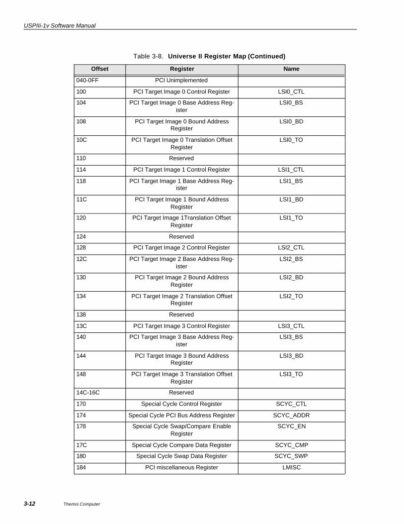
Table 3-8. Universe II Register Map (Continued)
Offset Register Name
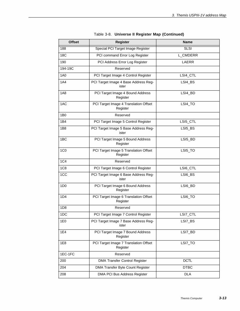
Themis Computer 3-13
3. Themis USPIIi-1V address Map
188 Special PCI Target Image Register SLSI
18C PCI command Error Log Register L_CMDERR
190 PCI Address Error Log Register LAERR
194-19C Reserved
1A0 PCI Target Image 4 Control Register LSI4_CTL
1A4 PCI Target Image 4 Base Address Reg-ister
LSI4_BS
1A8 PCI Target Image 4 Bound Address Register
LSI4_BD
1AC PCI Target Image 4 Translation Offset Register
LSI4_TO
1B0 Reserved
1B4 PCI Target Image 5 Control Register LSI5_CTL
1B8 PCI Target Image 5 Base Address Reg-ister
LSI5_BS
1BC PCI Target Image 5 Bound Address Register
LSI5_BD
1C0 PCI Target Image 5 Translation Offset Register
LSI5_TO
1C4 Reserved
1C8 PCI Target Image 6 Control Register LSI6_CTL
1CC PCI Target Image 6 Base Address Reg-ister
LSI6_BS
1D0 PCI Target Image 6 Bound Address Register
LSI6_BD
1D4 PCI Target Image 6 Translation Offset Register
LSI6_TO
1D8 Reserved
1DC PCI Target Image 7 Control Register LSI7_CTL
1E0 PCI Target Image 7 Base Address Reg-ister
LSI7_BS
1E4 PCI Target Image 7 Bound Address Register
LSI7_BD
1E8 PCI Target Image 7 Translation Offset Register
LSI7_TO
1EC-1FC Reserved
200 DMA Transfer Control Register DCTL
204 DMA Transfer Byte Count Register DTBC
208 DMA PCI Bus Address Register DLA
Table 3-8. Universe II Register Map (Continued)
Offset Register Name
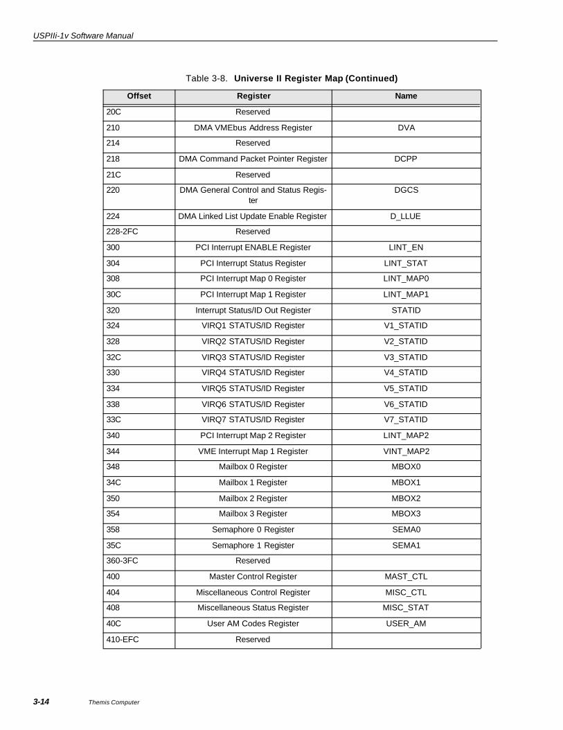
USPIIi-1v Software Manual
3-14 Themis Computer
20C Reserved
210 DMA VMEbus Address Register DVA
214 Reserved
218 DMA Command Packet Pointer Register DCPP
21C Reserved
220 DMA General Control and Status Regis-ter
DGCS
224 DMA Linked List Update Enable Register D_LLUE
228-2FC Reserved
300 PCI Interrupt ENABLE Register LINT_EN
304 PCI Interrupt Status Register LINT_STAT
308 PCI Interrupt Map 0 Register LINT_MAP0
30C PCI Interrupt Map 1 Register LINT_MAP1
320 Interrupt Status/ID Out Register STATID
324 VIRQ1 STATUS/ID Register V1_STATID
328 VIRQ2 STATUS/ID Register V2_STATID
32C VIRQ3 STATUS/ID Register V3_STATID
330 VIRQ4 STATUS/ID Register V4_STATID
334 VIRQ5 STATUS/ID Register V5_STATID
338 VIRQ6 STATUS/ID Register V6_STATID
33C VIRQ7 STATUS/ID Register V7_STATID
340 PCI Interrupt Map 2 Register LINT_MAP2
344 VME Interrupt Map 1 Register VINT_MAP2
348 Mailbox 0 Register MBOX0
34C Mailbox 1 Register MBOX1
350 Mailbox 2 Register MBOX2
354 Mailbox 3 Register MBOX3
358 Semaphore 0 Register SEMA0
35C Semaphore 1 Register SEMA1
360-3FC Reserved
400 Master Control Register MAST_CTL
404 Miscellaneous Control Register MISC_CTL
408 Miscellaneous Status Register MISC_STAT
40C User AM Codes Register USER_AM
410-EFC Reserved
Table 3-8. Universe II Register Map (Continued)
Offset Register Name
Themis Computer 3-15
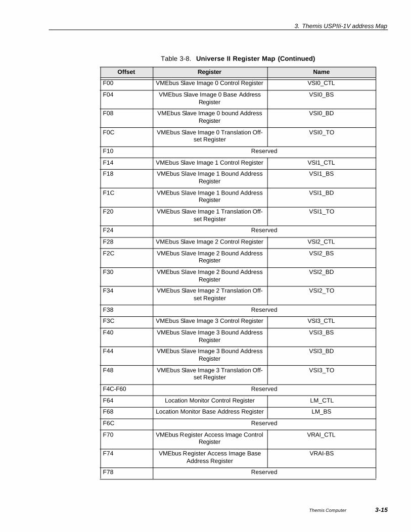
3. Themis USPIIi-1V address Map
F00 VMEbus Slave Image 0 Control Register VSI0_CTL
F04 VMEbus Slave Image 0 Base Address Register
VSI0_BS
F08 VMEbus Slave Image 0 bound Address Register
VSI0_BD
F0C VMEbus Slave Image 0 Translation Off-set Register
VSI0_TO
F10 Reserved
F14 VMEbus Slave Image 1 Control Register VSI1_CTL
F18 VMEbus Slave Image 1 Bound Address Register
VSI1_BS
F1C VMEbus Slave Image 1 Bound Address Register
VSI1_BD
F20 VMEbus Slave Image 1 Translation Off-set Register
VSI1_TO
F24 Reserved
F28 VMEbus Slave Image 2 Control Register VSI2_CTL
F2C VMEbus Slave Image 2 Bound Address Register
VSI2_BS
F30 VMEbus Slave Image 2 Bound Address Register
VSI2_BD
F34 VMEbus Slave Image 2 Translation Off-set Register
VSI2_TO
F38 Reserved
F3C VMEbus Slave Image 3 Control Register VSI3_CTL
F40 VMEbus Slave Image 3 Bound Address Register
VSI3_BS
F44 VMEbus Slave Image 3 Bound Address Register
VSI3_BD
F48 VMEbus Slave Image 3 Translation Off-set Register
VSI3_TO
F4C-F60 Reserved
F64 Location Monitor Control Register LM_CTL
F68 Location Monitor Base Address Register LM_BS
F6C Reserved
F70 VMEbus Register Access Image Control Register
VRAI_CTL
F74 VMEbus Register Access Image Base Address Register
VRAI-BS
F78 Reserved
Table 3-8. Universe II Register Map (Continued)
Offset Register Name

USPIIi-1v Software Manual
3-16 Themis Computer
F7C Reserved
F80 VMEbus CSR Control Register VCSR_CTL
F84 VMEbus CSR Translation Offset Regis-ter
VSCR_TO
F88 VMEbus AM Code Error Log Register V_AMERR
F8C VMEbus Address Error Log Register VAERR
F90 VMEbus Slave Image 4 Control Register VSI4_CTL
F94 VMEbus Slave Image 4 Bound Address Register
VSI4_BS
F98 VMEbus Slave Image 4 Bound Address Register
VSI4_BD
F9C VMEbus Slave Image 4 Translation Off-set Register
VSI4_TO
FA0 Reserved
FA4 VMEbus Slave Image 5 Control Register VSI5_CTL
FA8 VMEbus Slave Image 5 Bound Address Register
VSI5_BS
FAC VMEbus Slave Image 5 Bound Address Register
VSI5_BD
FB0 VMEbus Slave Image 5 Translation Off-set Register
VSI5_TO
FB4 Reserved
FB8 VMEbus Slave Image 6 Control Register VSI6_CTL
FBC VMEbus Slave Image 6 Bound Address Register
VSI6_BS
FC0 VMEbus Slave Image 6 Bound Address Register
VSI6_BD
FC4 VMEbus Slave Image 6 Translation Off-set Register
VSI6_TO
FC8 Reserved
FCC VMEbus Slave Image 7 Control Register VSI7_CTL
FD0 VMEbus Slave Image 7 Bound Address Register
VSI7_BS
FD4 VMEbus Slave Image 7 Bound Address Register
VSI7_BD
FD8 VMEbus Slave Image 7 Translation Off-set Register
VSI7_TO
FDC-FEC Reserved
FF0 VME CR/CSR Reserved
FF4 VMEbus CSR Bit Clear Register VCSR_CLR
Table 3-8. Universe II Register Map (Continued)
Offset Register Name

Themis Computer 3-17
3. Themis USPIIi-1V address Map
3.10 Ultra Fast/Wide SCSI Controller (SYMBIOS SYM53C876)
The SYMBIOS Ultra Fast/Wide SCSI Controller is located on PCI bus B. It has two PCI functions, as it ismanaging the two on-board SCSI interfaces.
FF8 VMEbus CSR Bit Set Register VCSR_SET
FFC VMEbus CSR Address Register VCSR_BS
Table 3-9. SCSI Controller Registers
Offset Register Access size
00 Vendor ID (0x1000) 2 bytes
02 Device ID (0x0001) 2 bytes
04 Primary command 2 bytes
06 Primary status 2 bytes
08 Revision ID 1 byte
09 Class code 3 bytes
0C Cache line size 1 byte
0D Primary Master Latency Timer 1 byte
0E Header type 1 byte
18 Primary Bus Number 1 byte
19 Secondary Bus Number A/B 1 byte
1A Subordinate Bus Number A/B 1 byte
1B Secondary Master Latency Timer A/B 1 byte
1E Secondary status A/B 2 bytes
3E Bridge Control A/B 2 bytes
Device specific registers:
B0 Tick register 4 bytes
B8 INT ACK Generation register A/B 4 bytes
C8 DMA AFSR A/B 8 bytes
D0 DMA AFAR A/B 1 byte
D8 PIO Target Retry Limit A/B 1 byte
D9 PIO target Latency Timer A/B 1 byte
DA DMA target Retry Limit A/B 1 byte
DB DMA Target Latency Timer A/B 1 byte
Table 3-8. Universe II Register Map (Continued)
Offset Register Name
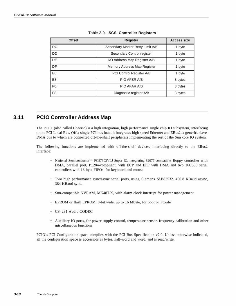
USPIIi-1v Software Manual
3-18 Themis Computer
3.11 PCIO Controller Address Map
The PCIO (also called Cheerio) is a high integration, high performance single chip IO subsystem, interfacingto the PCI Local Bus. Off a single PCI bus load, it integrates high speed Ethernet and EBus2, a generic, slave-DMA bus to which are connected off-the-shelf peripherals implementing the rest of the Sun core IO system.
The following functions are implemented with off-the-shelf devices, interfacing directly to the EBus2interface:
• National SemiconductorTM PC87303VLJ Super IO, integrating 82077-compatible floppy controller withDMA, parallel port, P1284-compliant, with ECP and EPP with DMA and two 16C550 serialcontrollers with 16-byte FIFOs, for keyboard and mouse
• Two high performance sync/async serial ports, using Siemens SAB82532. 460.8 KBaud async,384 KBaud sync.
• Sun-compatible NVRAM, MK48T59, with alarm clock interrupt for power management
• EPROM or flash EPROM, 8-bit wide, up to 16 Mbyte, for boot or FCode
• CS4231 Audio CODEC
• Auxiliary IO ports, for power supply control, temperature sensor, frequency calibration and othermiscellaneous functions
PCIO’s PCI Configuration space complies with the PCI Bus Specification v2.0. Unless otherwise indicated,all the configuration space is accessible as bytes, half-word and word, and is read/write.
DC Secondary Master Retry Limit A/B 1 byte
DD Secondary Control register 1 byte
DE I/O Address Map Register A/B 1 byte
DF Memory Address Map Register 1 byte
E0 PCI Control Register A/B 1 byte
E8 PIO AFSR A/B 8 bytes
F0 PIO AFAR A/B 8 bytes
F8 Diagnostic register A/B 8 bytes
Table 3-9. SCSI Controller Registers
Offset Register Access size

Themis Computer 3-19
3. Themis USPIIi-1V address Map
PCIO contains two PCI functions within a single device: EBus2 and Ethernet. These are implemented asfunctions 0 and 1 respectively. PCIO responds to configuration cycles for functions 2 to 7 indicating they arenot implemented (i.e. read zeroes from all locations.)
Table 3-10. PCIO Registers
Offset Register Access size
00 Vendor ID (0x108E) 2 bytes
02 Device ID (0x1000) 2 bytes
04 Command Register 2 bytes
06 Primary status 2 bytes
08 Revision ID 1 byte
09 Class code 3 bytes
0C Cache line size 1 byte
0D Primary Master Latency Timer 1 byte
0E Header type 1 byte
0xF BIST=0x00, not capable 1 byte
0x10-0x13 Base address Register of the 16MB Bootrom address space. Set to
0xF000.0000
4 byte
0x14-0x17 Base address Register of the 8MB EBus2 channel Engine space. Sets to
0xF100.0000
4 bytes
0x18-0x2F Reserved
0x30-0x33 Expansion Rom Base address 4 bytes
0x34-0x3B Reserved
0x3C Interrupt line 1 byte
0x3E Min_GNT = 0x0A in unites of 1/4 of a Microsecond = 6.25us
1 byte
0x3F Min_Lat = 0x19 in unites of 1/4 of a Micro-second = 6.25us
1 byte
0x40 Diagnostic Register 4 bytes
0x44-0xFF Reserved
Ethernet:
0x100-0x101 Vendor ID=0x108E 2 bytes
0x102-0x103 Device ID=0x1001 2 bytes
0x104-0x105 Command Register 2 bytes
0x106-0x107 Status Register 1 byte
0x108 Revision ID=0x01 1 byte
0x109-0x10B Class Code 3 bytes
0x10C Cache Line Size in unit of 32bit words 1 byte

USPIIi-1v Software Manual
3-20 Themis Computer
3.12 PCIO (CHEERIO) #1 EBUS Device Mapping
This table lists all devices that are managed by the PCIO #1 chip EBUS interface. This chip is located on theUSPII i-1v base board. Note that this chip also acts as Ethernet A controller.
0x10D Latency timer 1 byte
0x10E Header type 1 byte
0x10E BIST 1 byte
0x110-0x113 Base address Register of Ethernet Chan-nel Engine
8 bytes
0x114-0x117 Reserved
0x118-0x12F Reserved
0x130-0x133 Expansion ROM Base address 4 bytes
0x134-0x13B Reserved
0x13C Interrupt line 1 byte
0x13D Interrupt pin 1 byte
0x13E Min_GNT = 0x0A in unites of 1/4 of a Microsecond = 6.25us
1 byte
0x13F Min_Lat = 0x19 in unites of 1/4 of a Micro-second = 6.25us
1 byte
Table 3-11. PCIO #1 EBUS device mapping
Device Address Size
Boot Address Space 0 0x1FF.F000.0000 4MB
Boot Address Space 1 0x1FF.F040.0000 4MB
Boot Address Space 2 0x1FF.F080.0000 4MB
NVRAM/TOD 0x1FF.F100.0000 8KB
SUPER I/O SERIAL PORT 1 (TTYA-console) 0x1FF.F136.03F8 -
SUPER I/O SERIAL PORT 2 (TTYB) 0x1FF.F136.02F -
SAB SERIAL PORT 1 (TTYC) 0x1FF.F140.0000 -
SAB SERIAL PORT 2 (TTYD) 0x1FF.F140.0040 -
SUPER I/O Parallel port 0x1FF.f134.0278 -
DALLAS DS1620 Temp sensor 0x1FF.F110.0000
DALLAS DS1620 Temp sensor C/S register 0x1FF.F110.0004
Table 3-10. PCIO Registers (Continued)
Offset Register Access size

Themis Computer 3-21
3. Themis USPIIi-1V address Map
3.13 PCIO(CHEERIO) #2 EBUS Device Mapping
This table lists all devices that are managed by the PCIO #2 chip EBUS interface. This chip is located on theUSPIIi-1v I/O board (USPIIi-1v/2C and USPII i-1v/3 only). Note that this chip also acts as Ethernet Bcontroller.
3.14 VMEbus Reset Register
Writing to the following register will trigger a VME BUS SYSRESET. The USPIIi-1v board will not beaffected by this reset. This is useful for software originated reset. For example, using OBP
ok 1 1ff.f110.0001 1d spacec!
PCIO Power System Register 0x1FF.F172.4000 -
READY LED 0x1FF.F172.6000 -
Table 3-12. PCIO #2 EBUS device mapping
Device Address Size
CS423 AUDIO/CODEC 0x1FF.F120.0000 -
Table 3-13. VMEbus Reset Registe
Description Address Effect
VMEbus Reset Register 0x1FF.F110.0001 Writing to this regis-ter will reset VME-
bus
Table 3-11. PCIO #1 EBUS device mapping (Continued)
Device Address Size

USPIIi-1v Software Manual
3-22 Themis Computer

44UNIVERSE II: PCI-VME bridge
4.1 Introduction
This chapter describes some of the most used software features of the UNIVERSE II VME controller. Pleaserefer to Themis USPIIi-1V hardware manual as well as to the Universe II user’s manual (www.tundra.com)for details.
4.2 Universe as VME Bus Slave
The Universe II becomes a VME Slave whenever one of its 8 programmed slave images is accessed by aVMEbus master. This means that the VME address generated by the VMEbus master has to fall within theVME address range defined for that slave window.
Note: In order for a VMEbus slave image to respond to an incoming cycle, the PCI Master Interface must beenabled (Bit BM in the PCI_CSR register).
A slave window is programmed through the use of the following registers:
VSIx_CTL: VMEbus Slave Image #x Control Register. Provides general, VMEbus and PCI controls for thisslave image’s behavior
VSIx_BS: VMEbus Slave image #x Base Address Register. Contains the VME base address of the slavewindow.
VSIx_BD: VMEbus Slave Image #x Bound Address Register. Contains the VME upper address of the slavewindow.
VSIx_TO: VMEbus Slave Image #x Translation Offset register. Contains an Offset, that will be added to theVME address to generate the PCI address.
Themis Computer 4-1
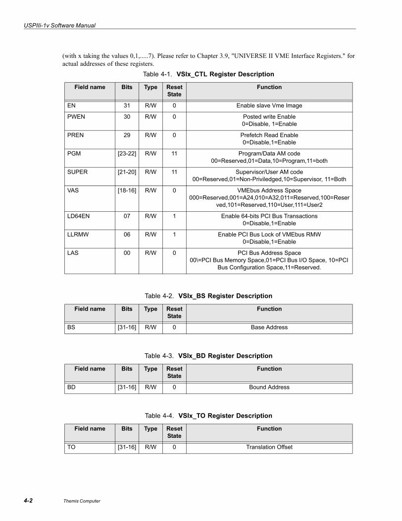
USPIIi-1v Software Manual
(with x taking the values 0,1,.....7). Please refer to Chapter 3.9, "UNIVERSE II VME Interface Registers." foractual addresses of these registers.
Table 4-1. VSIx_CTL Register Description
Field name Bits Type Reset State
Function
EN 31 R/W 0 Enable slave Vme Image
PWEN 30 R/W 0 Posted write Enable0=Disable, 1=Enable
PREN 29 R/W 0 Prefetch Read Enable0=Disable,1=Enable
PGM [23-22] R/W 11 Program/Data AM code00=Reserved,01=Data,10=Program,11=both
SUPER [21-20] R/W 11 Supervisor/User AM code00=Reserved,01=Non-Priviledged,10=Supervisor, 11=Both
VAS [18-16] R/W 0 VMEbus Address Space000=Reserved,001=A24,010=A32,011=Reserved,100=Reser
ved,101=Reserved,110=User,111=User2
LD64EN 07 R/W 1 Enable 64-bits PCI Bus Transactions0=Disable,1=Enable
LLRMW 06 R/W 1 Enable PCI Bus Lock of VMEbus RMW0=Disable,1=Enable
LAS 00 R/W 0 PCI Bus Address Space00\=PCI Bus Memory Space,01=PCI Bus I/O Space, 10=PCI
Bus Configuration Space,11=Reserved.
Table 4-2. VSIx_BS Register Description
Field name Bits Type Reset State
Function
BS [31-16] R/W 0 Base Address
Table 4-3. VSIx_BD Register Description
Field name Bits Type Reset State
Function
BD [31-16] R/W 0 Bound Address
Table 4-4. VSIx_TO Register Description
Field name Bits Type Reset State
Function
TO [31-16] R/W 0 Translation Offset
4-2 Themis Computer
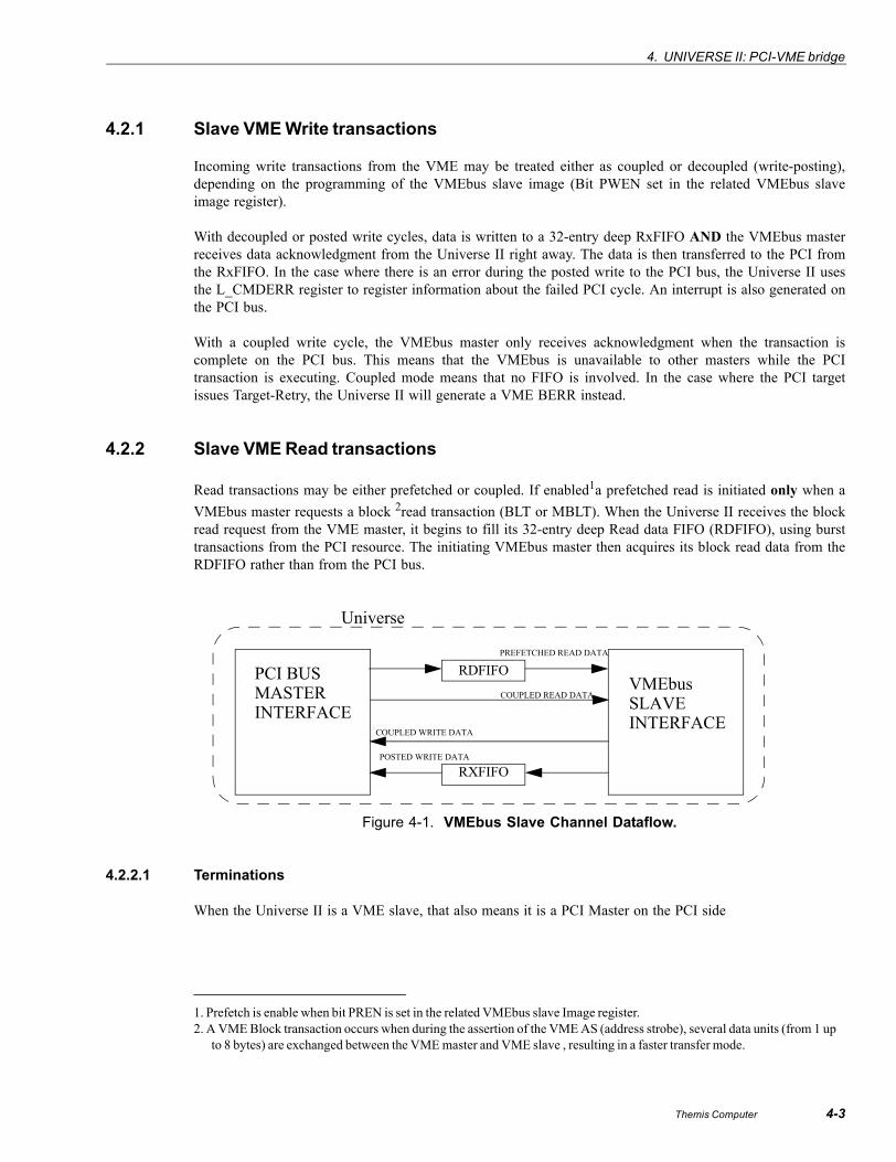
4. UNIVERSE II: PCI-VME bridge
4.2.1 Slave VME Write transactions
Incoming write transactions from the VME may be treated either as coupled or decoupled (write-posting),depending on the programming of the VMEbus slave image (Bit PWEN set in the related VMEbus slaveimage register).
With decoupled or posted write cycles, data is written to a 32-entry deep RxFIFO AND the VMEbus masterreceives data acknowledgment from the Universe II right away. The data is then transferred to the PCI fromthe RxFIFO. In the case where there is an error during the posted write to the PCI bus, the Universe II usesthe L_CMDERR register to register information about the failed PCI cycle. An interrupt is also generated onthe PCI bus.
With a coupled write cycle, the VMEbus master only receives acknowledgment when the transaction iscomplete on the PCI bus. This means that the VMEbus is unavailable to other masters while the PCItransaction is executing. Coupled mode means that no FIFO is involved. In the case where the PCI targetissues Target-Retry, the Universe II will generate a VME BERR instead.
4.2.2 Slave VME Read transactions
Read transactions may be either prefetched or coupled. If enabled1a prefetched read is initiated only when aVMEbus master requests a block 2read transaction (BLT or MBLT). When the Universe II receives the blockread request from the VME master, it begins to fill its 32-entry deep Read data FIFO (RDFIFO), using bursttransactions from the PCI resource. The initiating VMEbus master then acquires its block read data from theRDFIFO rather than from the PCI bus.
Figure 4-1. VMEbus Slave Channel Dataflow.
4.2.2.1 Terminations
When the Universe II is a VME slave, that also means it is a PCI Master on the PCI side
1. Prefetch is enable when bit PREN is set in the related VMEbus slave Image register.2. A VME Block transaction occurs when during the assertion of the VME AS (address strobe), several data units (from 1 up
to 8 bytes) are exchanged between the VME master and VME slave , resulting in a faster transfer mode.
VMEbusSLAVE INTERFACE
PCI BUS MASTERINTERFACE
RDFIFO
RXFIFO
COUPLED READ DATA
PREFETCHED READ DATA
COUPLED WRITE DATA
POSTED WRITE DATA
Universe
Themis Computer 4-3
USPIIi-1v Software Manual
The Universe II performs a Master-Abort if the target does not respond within 6 clock cycles. Coupled PCItransactions terminated with Target-Abort or Master-Abort are terminated on the VMEbus with BERR*. TheR_TA or R_MA bits in the PCI_CS register are set when the Universe II receives a Target-Abort or generatesa Master-Abort independent of whether the transaction was coupled, decoupled, prefetched, or initiated by theDMA. If the Universe II receives a retry from the PCI target, then it relinquishes the PCI bus and re-requestswithin 2-3 PCI clock cycles. No other transactions are processed by the PCI Master Interface until the retrycondition is cleared. The Universe II can be programmed to perform a maximum number of retries using theMAXRTRY field in the MAST_CTL register. When this number of retries has been reached, the Universe IIresponds in the same way as it does to a Target-Abort on the PCI bus. That is, the Universe II may issue aBERR* signal on the VMEbus. All VMEbus slave coupled transactions and decoupled transactions willencounter a delayed DTACK once the FIFO fills until the condition clears either due to success or a retrytime-out. If the error occurs during a posted write to the PCI bus, the Universe II uses the L_CMDERRregister to log the command information for the transaction (CMDERR [3:0]) and the address of the erroredtransaction is latched in the LAERR register. The L_CMDERR register also records if multiple errors occur(with the M_ERR bit) although the number of errors is not given. The error log is qualified with the L_STATbit. The rest of the transaction will be purged from the RXFIFO if some portion of the write encounters anerror. An interrupt is generated on the VMEbus and/or PCI bus depending upon whether the VERR andLERR interrupts are enabled.
If an error occurs on the PCI bus, the Universe II does not translate the error condition into a BERR* on theVMEbus. Indeed, the Universe II does not directly map the error. By doing nothing, the Universe II forces theexternal VMEbus error timer to expire.
4.3 Universe as VMEbus Master
The UNIVERSE II becomes a VMEbus master when one of its eight programmed PCI target images isaccessed by a PCI bus master.
A PCI target image is programmed using the following registers:
LSIx_CTL: PCI target image #x control
LSIx_BS: PCI target Image #x Base address Register
LSIx_BD: PCI target image #x Bound address Register.
LSIx_TO: PCI Target Image #x translation Offset
Table 4-5. LSIx_CTL Register Description
Field name Bits Type Reset State
Function
EN 31 R/W Power up
option
Enable slave Vme Image
PWEN 30 R/W 0 Posted write Enable0=Disable, 1=Enable
4-4 Themis Computer

4. UNIVERSE II: PCI-VME bridge
Read transactions are always coupled. Write transactions can be coupled or posted. To ensure sequentialconsistency, coupled operations (reads or writes) are only processed one all previously posted write operationshave completed(i.e the TXFIFO is empty).
VDW [23-22] R/W 10 VMEbus Maximum Datawidth00=8 bits,01=16 bits,10=32 bits,64bits
VAS [18-16] R/W 0 VMEbus Address Space000=Reserved,001=A24,010=A32,011=Reserved,100=Reser
ved,101=Reserved,110=User,111=User2
PGM 14 R/W 0 Program/Data AM code0=Data,1=Program
SUPER 12 R/W 11 Supervisor/User AM code0=Non-Priviledged,1=Supervisor
VCT 08 R/W 0 VMEbus Cycle type0=No BLTS on VME,1=Single BLTs on VME
LAS 0 R/W Power up
option
PCI Bus Memory Space0=PCI Bus Memory Space,1=PCI Bus I/O Space
Table 4-6. LSIx_BS Register Description
Field name Bits Type Reset State
Function
BS [31-28] R/W Power up
Option
Base Address
BS [27-12] R/W 0 Base Address
Table 4-7. LSIx_BD Register Description
Field name Bits Type Reset State
Function
BD [31-28] R/W Power up
Option
Bound Address
Table 4-8. LSIx_TO Register Description
Field name Bits Type Reset State
Function
TO [31-12] R/W 0 Translation Offset
Table 4-5. LSIx_CTL Register Description
Field name Bits Type Reset State
Function
Themis Computer 4-5
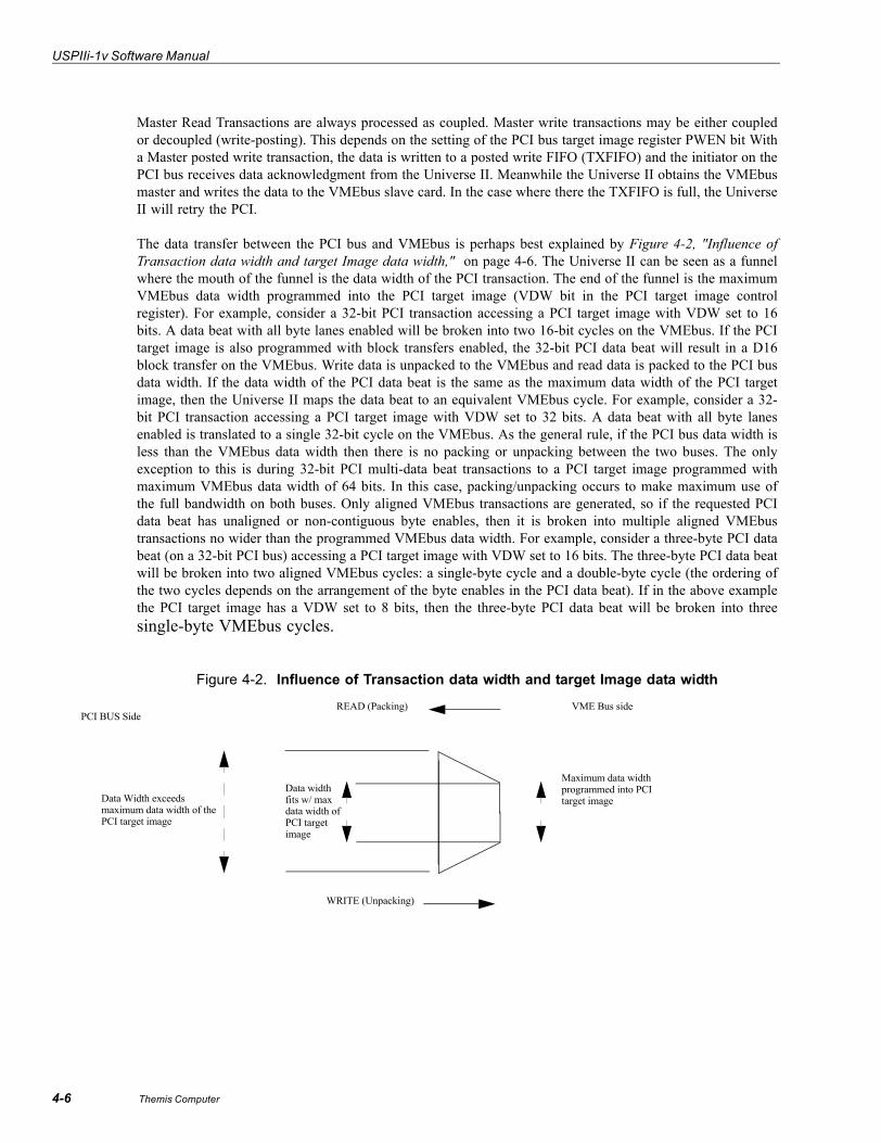
USPIIi-1v Software Manual
Master Read Transactions are always processed as coupled. Master write transactions may be either coupledor decoupled (write-posting). This depends on the setting of the PCI bus target image register PWEN bit Witha Master posted write transaction, the data is written to a posted write FIFO (TXFIFO) and the initiator on thePCI bus receives data acknowledgment from the Universe II. Meanwhile the Universe II obtains the VMEbusmaster and writes the data to the VMEbus slave card. In the case where there the TXFIFO is full, the UniverseII will retry the PCI.
The data transfer between the PCI bus and VMEbus is perhaps best explained by Figure 4-2, "Influence ofTransaction data width and target Image data width," on page 4-6. The Universe II can be seen as a funnelwhere the mouth of the funnel is the data width of the PCI transaction. The end of the funnel is the maximumVMEbus data width programmed into the PCI target image (VDW bit in the PCI target image controlregister). For example, consider a 32-bit PCI transaction accessing a PCI target image with VDW set to 16bits. A data beat with all byte lanes enabled will be broken into two 16-bit cycles on the VMEbus. If the PCItarget image is also programmed with block transfers enabled, the 32-bit PCI data beat will result in a D16block transfer on the VMEbus. Write data is unpacked to the VMEbus and read data is packed to the PCI busdata width. If the data width of the PCI data beat is the same as the maximum data width of the PCI targetimage, then the Universe II maps the data beat to an equivalent VMEbus cycle. For example, consider a 32-bit PCI transaction accessing a PCI target image with VDW set to 32 bits. A data beat with all byte lanesenabled is translated to a single 32-bit cycle on the VMEbus. As the general rule, if the PCI bus data width isless than the VMEbus data width then there is no packing or unpacking between the two buses. The onlyexception to this is during 32-bit PCI multi-data beat transactions to a PCI target image programmed withmaximum VMEbus data width of 64 bits. In this case, packing/unpacking occurs to make maximum use ofthe full bandwidth on both buses. Only aligned VMEbus transactions are generated, so if the requested PCIdata beat has unaligned or non-contiguous byte enables, then it is broken into multiple aligned VMEbustransactions no wider than the programmed VMEbus data width. For example, consider a three-byte PCI databeat (on a 32-bit PCI bus) accessing a PCI target image with VDW set to 16 bits. The three-byte PCI data beatwill be broken into two aligned VMEbus cycles: a single-byte cycle and a double-byte cycle (the ordering ofthe two cycles depends on the arrangement of the byte enables in the PCI data beat). If in the above examplethe PCI target image has a VDW set to 8 bits, then the three-byte PCI data beat will be broken into threesingle-byte VMEbus cycles.
Figure 4-2. Influence of Transaction data width and target Image data width
PCI BUS SideVME Bus sideREAD (Packing)
WRITE (Unpacking)
Maximum data width programmed into PCItarget imageData Width exceeds
maximum data width of thePCI target image
Data widthfits w/ maxdata width of PCI targetimage
4-6 Themis Computer
4. UNIVERSE II: PCI-VME bridge
4.3.1 Coupled Transfers
The PCI Target Channel supports “coupled transfers”. In a nutshell, a coupled transfer through the PCI TargetChannel is a transfer between PCI and VME where the Universe II maintains ownership of the VMEbus fromthe beginning to the end of the transfer on the PCI bus (and possibly longer), and where the termination of thecycle on the VMEbus is relayed directly to the PCI initiator in the normal manner (i.e., Target-Abort, orTarget Completion), rather than through error-logging and interrupts.By default, all PCI target images are setfor coupled transfers. Coupled transfers typically cause the Universe II to go through three phases: TheCoupled Request Phase, the Coupled Data-Transfer Phase, and then the Coupled Wait Phase. When anexternal PCI Master attempts a data transfer through a slave image programmed for coupled cycles, then:
• If the Universe II currently owns the VMEbus, the PCI Target Channel moves directly to the Coupled Data-Transfer Phase; otherwise,
• the Universe II moves to the Coupled Request Phase. These three phases are described below.
Note that once the Coupled Request phase has begun, posted writes may traverse the PCI Target Channelwithout affecting coupled transfers.
Coupled Request Phase
During the Coupled Request Phase, the Universe II will attempt to acquire the VMEbus. But first it mustempty any posted writes pending in the TXFIFO, and obtain ownership of the internal VMEbus MasterInterface for more details on how the Universe II shares the VMEbus between channels.) The PCI TargetChannel retries the PCI master until the PCI Target Channel obtains ownership of the VMEbus. Every time itissues such a retry, the Universe II restarts the Coupled Request Timer, which counts down a period of 2 15PCI clock cycles. The Coupled Request Timer co-determines how long the Universe II maintains the VMEbussince the last time the Universe II issued a Target-Retry during a Coupled Request Phase: the Universe II willrelease (or terminate its attempt to obtain) the VMEbus if a coupled transfer is not attempted before theCoupled Request Timer expires. Usually, an external PCI Master will attempt a coupled cycle once theUniverse II has acquired the VMEbus during its Coupled Request Phase. In this case the Universe willproceed to the “Coupled Data-Transfer Phase”. No address matching is performed to verify whether thecurrent coupled cycle matches the initiating coupled cycle. If an external PCI Master requests a PCI I/O orRMW transfer with an illegal byte lane combination, the Universe II will exit the “Coupled Request Phase.”
Coupled Data-Transfer Phase
At the beginning of the Coupled Data-Transfer Phase, the Universe II latches the PCI command, byte enable,address and (in the case of a write) data. Regardless of the state of FRAME#, the Universe II retries 1 themaster, and then performs the transaction on the VMEbus. The Universe II continues to signal Target-Retry tothe external PCI master until the transfer completes (normally or abnormally) on the VMEbus. If the transfercompletes normally on the VMEbus, then in the case of a read, the data is transmitted to the PCI bus master.If a data phase of a coupled transfer requires packing or unpacking on the VMEbus, acknowledgment of thetransfer is not given to the PCI bus master until all data has been packed or unpacked on the VMEbus.Successful termination is signalled on the PCI bus—the data beat is acknowledged with a Target-Disconnect,forcing all multi-beat transfers into single beat. At this point, the Universe II enters the Coupled Wait Phase.
If a bus error is signalled on the VMEbus or an error occurs during packing or unpacking, then the transactionis terminated on the PCI bus with Target-Abort.
Themis Computer 4-7

USPIIi-1v Software Manual
Coupled Wait Phase
The Coupled Wait Phase is entered after the successful completion of a Coupled Data-Transfer phase. TheCoupled Wait Phase allows consecutive coupled transactions to occur without releasing the VMEbus. If a newcoupled transaction is attempted while the Universe II is in the Coupled Wait Phase, the Universe II willmove directly to the Coupled Data-Transfer Phase without reentering the Coupled Request Phase.
The Coupled Window Timer determines the maximum duration of the Coupled Wait Phase. When theUniverse II enters the Coupled Wait Phase, the Coupled Window Timer starts. The period of this timer isspecified in PCI clocks and is programmable through the CWT field of the LMISC register (Table A.30). Ifthis field is programmed to 0000, the Universe II will do an early release of BBSY* during the coupledtransfer on the VMEbus and will not enter the “Coupled Wait Phase.” In this case, VMEbus ownership isrelinquished immediately by the PCI Target Channel after each coupled cycle.
Once the timer associated with the Coupled Wait Phase expires, the Universe II will release the VMEbus ifrelease mode is set for RWD, or the release mode is set for ROR and there is a pending (external) request onthe VMEbus.
4.3.2 Posted Writes
Posted writes are enabled for a PCI target image by setting the PWEN bit in the control register of the PCItarget image. Write transactions are relayed from the PCI bus to the VMEbus through a 32-entry deepTXFIFO. The TXFIFO allows each entry to contain 32 address bits (with extra bits provided for commandinformation), or up to 64 data bits. For each posted write transaction received from the PCI bus, the PCITarget Interface queues an address entry in the FIFO. This entry contains the translated address space andmapped VMEbus attributes information relevant to the particular PCI target image that has been accessed. Forthis reason, any reprogramming of PCI bus target image attributes will only be reflected in TXFIFO entriesqueued after the reprogramming. Transactions queued before the reprogramming are delivered to the VMEbuswith the PCI bus target image attributes that were in use before the reprogramming.
Caution: Care should be taken before reprogramming target images from one bus while that image is beingaccessed from the opposite bus. If there is a chance the image may be accessed while being reprogrammed,disable the image first before changing image attributes. Once the address phase is queued in one TXFIFOentry, the PCI Target Interface may pack the subsequent data beats to a full 64-byte width before queuing thedata into new entries in the TXFIFO. For 32-bit PCI transfers in the Universe II, the TXFIFO will accept asingle burst of one address phase and 59 data phases when it is empty. For 64-bit PCI, the TXFIFO willaccept a single burst of one address phase and 31 data phases when it is empty. To improve PCI busutilization, the TXFIFO does not accept a new address phase if it does not have room for a burst of oneaddress phase and 128 bytes of data. If the TXFIFO does not have enough space for an aligned burst, then theposted write transaction is terminated with a Target-Retry immediately after the address phase.
When an external PCI Master posts writes to the PCI Target Channel of the Universe II, the Universe II willissue a disconnect if the implied address will cross a 256-byte boundary. Before a transaction can be deliveredto the VMEbus from the TXFIFO, the PCI Target Channel must obtain ownership of the VMEbus MasterInterface. Ownership of the VMEbus Master Interface is granted to the different channels on a round robinbasis. Once the PCI Target Channel obtains the VMEbus through the VMEbus Master Interface, the mannerin which the TXFIFO entries are delivered depends on the programming of the VMEbus attributes in the PCItarget image. For example, if the VMEbus data width is programmed to 16 bits, and block transfers aredisabled, then each data entry in the TXFIFO corresponds to four transactions on the VMEbus.
4-8 Themis Computer

4. UNIVERSE II: PCI-VME bridge
If block transfers are enabled in the PCI target image, then each transaction queued in the TXFIFO,independent of its length, is delivered to the VMEbus as a block transfer. This means that if a single data beattransaction is queued in the TXFIFO, it appears on the VMEbus as a single data phase block transfer. AnyPCI master attempting coupled transactions is retried while the TXFIFO contains data. If posted writes arecontinually written to the PCI Target Channel, and the FIFO does not empty, coupled transactions in the PCITarget Channel will not proceed and will be continually retried. This presents a potential starvation scenario.
4.3.3 Terminations
The Universe II performs the following terminations as PCI target:
4.3.3.1 Target-Disconnect
- when registers are accessed with FRAME# asserted (no bursts allowed to registers),
- after the first data beat of every coupled cycle, or
- after the first data phase of a PCI Memory command (with FRAME# asserted) if AD[1:0] is not equal to 00,as recommended in Revision 2.1 of the PCI Specification .
4.3.3.2 Target-Retry
- for 64-bit PCI, when a new posted write is attempted and the TXFIFO does not have room for a burst of oneaddress phase and sixteen 64-bit data phases, - when a coupled transaction is attempted and the Universe IIdoes not own the VMEbus,
- when a coupled transaction is attempted while the TXFIFO has entries to process, or
- when a master attempts to access the Universe II’s registers while a VMEbus
master owns the Register Channel (e.g., through a RMW access or another type of access).
4.3.3.3 Target-Abort
- when the Universe II receives BERR* on the VMEbus during a coupled cycle (BERR* translated as Target-Abort on the PCI side and the S_TA bit is set in the PCI_CS register.
Whether to terminate a transaction or for retry purposes, the Universe II keeps STOP# asserted untilFRAME# is deasserted, independent of the logic levels of IRDY# and TRDY#.
If STOP# is asserted while TRDY# is deasserted, it means that the Universe II will not transfer any more datato the master. If an error occurs during a posted write to the VMEbus, the Universe II uses the V_AMERRregister to log the AM code of the transaction (AMERR [5:0]), and the state of the IACK* signal (IACK bit,to indicate whether the error occurred during an IACK cycle).
The FIFO entries for the offending cycle are purged. The V_AMERR register also records whether multipleerrors have occurred (with the M_ERR bit) although the number is not given. The error log is qualified withthe V_STAT bit (logs are valid if the V_STAT bit is set).
Themis Computer 4-9
USPIIi-1v Software Manual
The address of the errored transaction is latched in the VAERR register. When the Universe II receives aVMEbus error during a posted write, it generates an interrupt on the VMEbus and/or PCI bus depending uponwhether the VERR and VERR interrupts are enabled.
4.4 Universe DMA controller
The Universe II provides an internal DMA controller for high performance data transfer between the PCI andthe VMEbus. DMA operations between the source and destination bus are decoupled through the use of asingle bidirectional FIFO (DMAFIFO)
The principal mechanism for DMA transfers is the same for operations in either direction (PCI to VMEbus, orVMEbus to PCI). In a DMA transfer, the Universe gains control of the source bus and reads data into itsDMAFIFO, following specific rules of DMAFIFO operation. It then acquires the destination bus and writesdata from its DMAFIFO.
4.5 Universe as a VME Requester
4.5.1 Requesting VMEbus
The Universe will request VME ownership in 3 different cases:
• The CPU needs to access the VMEbus, via a PCI bus cycle.
• The Universe has detected an enabled VMEbus interrupt (meaning there is currently a VMEinterrupt and it is enabled by the Universe LINT_EN register) and needs to run an interruptacknowledge cycle to acquire the interrupt vector from the VME interrupter board.
• The Universe DMA controller needs to transfer data to/from VMEbus.
The Universe is software configurable (VRL bits in MAST_CTL) to request on all VMEbus request level:BR3,2,1,0. Default setting is BR3.
The Universe may request the VMEbus for either FAIR or DEMAND mode (VRM bits in MAST_CTLregister):
• In FAIR mode, the Universe will not request the VMEbus until there are no other VMEbusrequests pending at its programmed level. This mode ensures that every requester on an equallevel has access to the VMEbus.
• In DEMAND mode, the requester asserts its bus request regardless of the state of the BRn line.Requesters far down the daisy chain1 may be prevented from ever obtaining VMEbus ownership.
In order to achieve fairness all bus requesters should be set to FAIR mode.
4-10 Themis Computer
4. UNIVERSE II: PCI-VME bridge
4.5.2 Releasing VMEbus
The Universe II requester can be configured as either RWD (release when done) or ROR (release on request).(VREL bits in MAST_CTL).
ROR means that the Universe releases the VMEbus (by no longer asserting VMEbus BBSY signal), only if abus request is pending from another VMEbus master.
IN RWD mode, the Universe released the VMEbus when it is done with its current VME cycle. A re-arbitration is required for subsequent VMEbus cycles from the Universe.
4.6 VME Cycle Terminations
The Universe only accepts BERR or DTACK as cycle terminations from the VMEbus slave card it istransferring data to/from.
A VMEbus BERR received by the Universe during a coupled transaction is communicated to the PCI masteras a Target-Abort. No information is logged in if the Universe receives BERR in a coupled transaction.
If an error occurs during a posted write to the VMEbus, the Universe uses the V_AMERR and V_AERRregisters to log information about the failed cycle. The Universe will generate an interrupt to the PCI bus inthis case.
4.7 Universe as a System Controller
4.7.1 VMEbus Configuration-First Slot Detector
As specified by the VME64 specification the first slot detector module on the Universe samples BG3INimmediately after reset to determine whether the Universe ‘s host board resides in VME slot1. The VMEbusspecification requires that BG[3:0] lines be driven high after reset. This means that if a card is preceded byanother card in the VMEbus system, it will always sample BG3IN high after reset. BG3IN can only besampled low after reset by the first card in the system, as there is no preceding card to drive BG3IN high). IfBG3IN is sampled at logic low immediately after reset (due to Universe internal pull-down), then theUniverse host board is said to be in slot 1 and the Universe becomes SYSCON.
This mechanism may be overridden by software through clearing/setting the SYSCON bit in the MISC_CTLregister.
1. VMEbus arbitration is done using the 4 BUS GRANT (BGn) daisy chain signals, which correspond to the 4 requester levels (BRn). These signals run from the SYSCON (top left board) to the next board on its right, which then passes them to the next right board if it is not requesting the VMEbus, and so on. A non SYSCON VME board can access the VMEbus only when it has received the GRANT from the SYSCON. This may never happen if a DEMAND requester is on its left, that keeps asking for the VMEbus.
Themis Computer 4-11

USPIIi-1v Software Manual
NOTE: The Universe monitors IACK rather than IACKIN when it is configured as SYSCON. This permits itto operate as SYSCON in a VMEbus chassis slot other than slot 1, provided there are only empty slots to itsleft. See Figure 4-3, "Universe is sampling IACK rather than IACKIN," on page 4-12
Figure 4-3. Universe is sampling IACK rather than IACKIN
4.8 VMEbus time out
A programmable bus timer allows users to select a VMEbus time-out period. The time-out period isprogrammed through the VBTO filed in the MISC_CTL register. It can be set to:
• 16us
• 32us
• 64us
• 128us
• 256us
• 512us
• 1024us
Vme Card 1(seen from above)
Vme Card 2(seen from above)
IACK signaldriven by interrupthandler VME cards
IACK signalis being loopedback ontoIACKIN inslot 1
No VME card in slot 1: IACKIN is not propagated to Vme!Card 1!
2 1
to initiate IACK cycleFor the case where the interrupter board in onthe left of the interrupt handler board, VME chassisare always looping backIACK to IACKIN[slot1]
is
.
Thus, the interrupter boardwill see IACKIN, and will respond to the IACK cycleby providing its interruptvector.
But this is not happening inthe case, where a slot isempty. So the Universesamples IACK rather than IACKIN.
IRQ
0
Step 0: Vme Card 1 is a Themis USPIIi-1V board with Universe chip.VME Card 1 (Vme slot 2) is
Step 1: Card 2 is initiating an IACK cycle, to get the interrupt vector.Step 2: The Universe chip in slot 2, is sampling IACK rather than IACKIN.
sending a VME Interrupt to Card2 (Vme slot 3).
4-12 Themis Computer
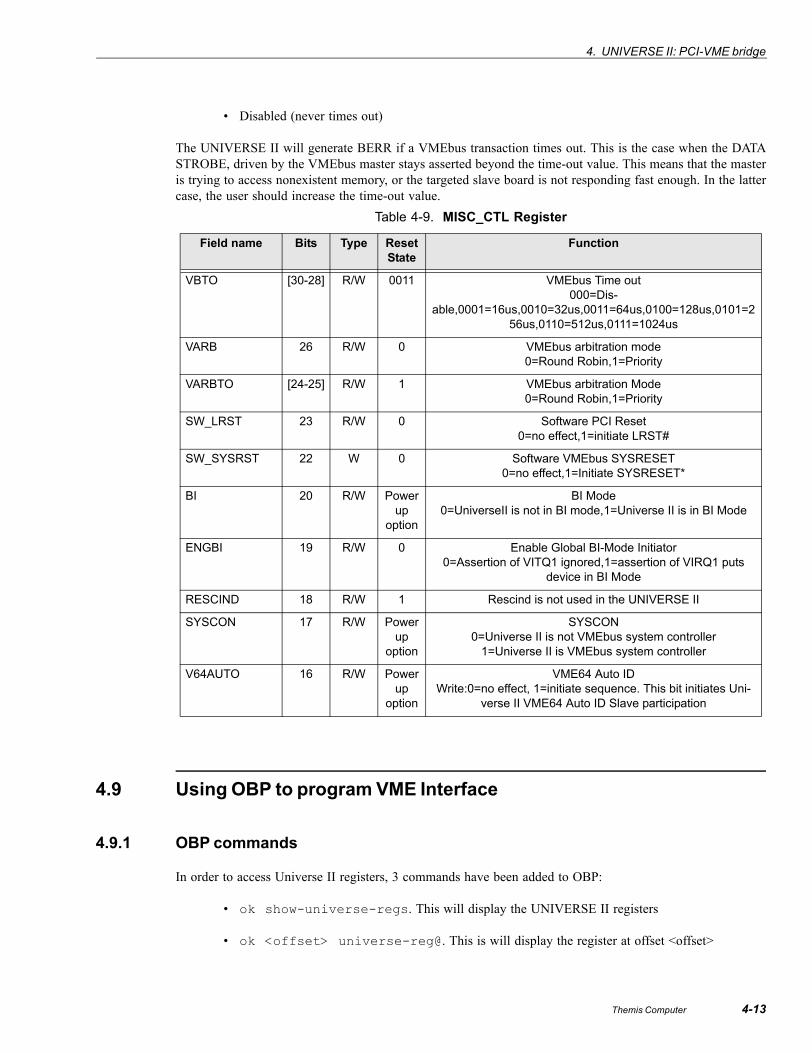
4. UNIVERSE II: PCI-VME bridge
• Disabled (never times out)
The UNIVERSE II will generate BERR if a VMEbus transaction times out. This is the case when the DATASTROBE, driven by the VMEbus master stays asserted beyond the time-out value. This means that the masteris trying to access nonexistent memory, or the targeted slave board is not responding fast enough. In the lattercase, the user should increase the time-out value.
4.9 Using OBP to program VME Interface
4.9.1 OBP commands
In order to access Universe II registers, 3 commands have been added to OBP:
• ok show-universe-regs. This will display the UNIVERSE II registers
• ok <offset> universe-reg@. This is will display the register at offset <offset>
Table 4-9. MISC_CTL Register
Field name Bits Type Reset State
Function
VBTO [30-28] R/W 0011 VMEbus Time out000=Dis-
able,0001=16us,0010=32us,0011=64us,0100=128us,0101=256us,0110=512us,0111=1024us
VARB 26 R/W 0 VMEbus arbitration mode0=Round Robin,1=Priority
VARBTO [24-25] R/W 1 VMEbus arbitration Mode0=Round Robin,1=Priority
SW_LRST 23 R/W 0 Software PCI Reset0=no effect,1=initiate LRST#
SW_SYSRST 22 W 0 Software VMEbus SYSRESET0=no effect,1=Initiate SYSRESET*
BI 20 R/W Power up
option
BI Mode0=UniverseII is not in BI mode,1=Universe II is in BI Mode
ENGBI 19 R/W 0 Enable Global BI-Mode Initiator0=Assertion of VITQ1 ignored,1=assertion of VIRQ1 puts
device in BI Mode
RESCIND 18 R/W 1 Rescind is not used in the UNIVERSE II
SYSCON 17 R/W Power up
option
SYSCON0=Universe II is not VMEbus system controller
1=Universe II is VMEbus system controller
V64AUTO 16 R/W Power up
option
VME64 Auto IDWrite:0=no effect, 1=initiate sequence. This bit initiates Uni-
verse II VME64 Auto ID Slave participation
Themis Computer 4-13

USPIIi-1v Software Manual
• ok <data> <offset> universe-reg! . This will write the value <data> into register atoffset <offset>
4.9.2 OBP Environment variables
OBP has been modified to include environment variables to help program and control the VME interface.These variables are to be programmed using the “setenv” OBP command:
Table 4-10. OBP Variables for VME Control
Name Default Value Description
vme32-slave-base 0 Slave window address in A32 mode
vme24-slave-base 0 Slave window address in A24 mode
vme32-slave-size 8388608(0x800000) Slave window address in A32 mode
vme24-slave-size 1048576(0x100000) Slave window size in A24 mode
vme-irq-to-service VME Interrupt to be serviced by a VME leaf driver.
vme-bus-request-level 3 Level used to request VMEbus
vme-arbitration-mode priority If Universe II is SYSCON: Arbitration mode used
vme-release-mode ror When the Universe II releases VMEbus, it is going to use either ROR (release or request) or RWD (release when done)
vme-request-mode demand When the Universe II requests the VME-bus, it is going to use either demand or
FAIR mode
vme32-master-base 0 Defines a master window on VME. All subsequent VME mappings that fall within this window will use the same
Universe II master window
vme32-master-size 0 Size of the above mentioned master window. Needs to be less than 256MB.
4-14 Themis Computer

55USPIIi-1V Interrupts
5.1 Overview
The UltraSPARCIIi CPU interrupt mechanism is based on the SPARC V9 “Mondo interrupt transfermechanism”. This mechanism features interrupt packets being delivered to the CPU over the UPA bus. But onthe UltraSPARCIIi CPU things are simpler as this mechanism is occurring internally to the CPU.
The “Mondo” interrupt transfer mechanism for Sun4u systems reduces interrupt service overhead by directlyidentifying the unique interrupter, without polling multiple status registers.
An interrupt packet contains a Mondo vector which has three double words designed to assist the processor inservicing the interrupt. Limitations of the Mondo vector approach include:
Only one interrupt request packet can be serviced at a time.
There is no priority level associated with Mondo vector interrupts; they are serviced on a first come, first servedbasis.
This interrupt packet delivery now happens inside the UltraSPARC-IIi CPU, rather than being visible on theUPA interconnect. Since it is an internal dedicated uniprocessor path, the flow control issues are simpler, andno interrupt retry is needed. UltraSPARC-IIi just causes one interrupt packet delivery at a time, after eachacknowledgment by software (clearing of the BUSY bit in the Interrupt Mapping Register in the Mondoreceive trap handler).
Themis Computer 5-1

USPIIi-1v Software Manual
Figure 5-1. Interrupt Logic.
SPARC V9 processors provide a dedicated set of registers to be used exclusively for servicing interrupts. Thiseliminates the need for the processor to save its current register set to service an interrupt, and then restore it later.There is a unique interrupt number register or INR for each interrupt source. These numbers are defined in theUltraSPARCIIi User’s manual (table11-4), and are also programmed in the interrupt mapping registers.Please refer to Chapter 3.6, "UltraSPARC-IIi PCI Control and Status Registers,"
5.2 Mondo Dispatch Overview
UltraSPARC-IIi’s PIE logic block is responsible for fielding interrupts from external PCI sources, otherexternal sources, and internal UltraSPARC-IIi resources, loading the Mondo data receive registers, andsignalling a Mondo receive trap to the UltraSPARC-IIi pipeline.
External interrupt sources include PCI slots on three separate PCI busses, the onboard IO devices, a graphicsinterrupt, and the expansion UPA slot. These interrupts are concentrated in an external ASIC (RIC) andpresented to the Mondo Unit one at a time. This saves pins on UltraSPARC-IIi. Internal interrupt sourcesinclude ECC (memory errors) and PBM (PCI bus errors). The CPU can process only one interrupt at a time.The Mondo Dispatch Unit is responsible for remembering all interrupts that have arrived, and serializing themto the CPU pipeline as traps. In addition, it tracks the state of pending DMA writes in the APB andUltraSPARC-IIi, and guarantees that all DMA writes complete on the Secondary PCI buses (temporally)before a PCI interrupt request, complete to memory before notifying the CPU. This is for the case, where theinterrupt routine is called prior to the DMA transfer not being done, potentially resulting in data structures being notcoherent.
5.3 UltraSPARCIIi Interrupt Registers
The UltraSPARCIIi registers involved for interrupt processing are:
• Interrupt mapping registers.
RIC
PIELogicBlock
CPUPipeline
MondoReceiveTrap
UltraSPARC IIiCPU
Interrupt requestslines
INT_NUM <5,0>
5-2 Themis Computer

5. USPIIi-1V Interrupts
• Incoming Interrupt Vector Data <2:0>
• Clear Interrupt Register
• Softint register
5.3.1 Interrupt Mapping Registers
Each source of interrupt has a mapping register associated to it. These registers must be initialized bysoftware. They act as an “enable interrupt register”, since the only bit that is writable is the “valid” bit. Therest of the information is hard-wired into these registers.
5.3.2 Interrupt Vector Data Register
UltraSPARC-IIi maintains an interrupt number lookup table. The Interrupt Vector Data Register in UltraSPARC-IIiis used to store the INR created from this lookup. After an Interrupt Vector Data Register is loaded with data,the UltraSPARC-IIi core must not receive another interrupt until it empties the register. Loading interrupt datainto an Interrupt Vector Data Register sets the Interrupt Vector Receive Register “Busy” bit. This bit indicatesto the UltraSPARCIIi IO that it must neither send another interrupt to the UltraSPARC-IIi core, nor load anInterrupt Vector Data Register until this bit is cleared. The “Busy” bit can also be cleared by software. Afterthe UltraSPARC-IIi core receives the interrupt, an interrupt trap is generated if IE bit of PSTATE Register is setto 1. The trap type for the interrupt trap is II 0x60.
INR is an 11 bit interrupt number that indicates the source of the interrupt. Where possible, the interrupt isprecise (that is, it points to only one interrupt source). This singularity permits the dispatch of the properinterrupt service routine without any register polling.
Table 5-1. Interrupt Mapping register definition
Field Bits Description POR State Type
Reserved 63:32 Reserved read as 0 0 R
V 31 Valid bit. When set to 0, any incoming interrupt will not be dispatched to CPU. Has no other impact on interrupt state.
0 R/W
Reserved 30:11 Reserved. Read as 0 0 RO
IGN 10:6 Interrupt Group Number: Read as 0x1F 0 RO
INO 5:0 Interrupt Number Offset: The value of this field is hardwired for each mapping regis-
ter.
- R
Table 5-2. Interrupt Receive Data Register
Name Bits Description
Interrupt RCV Data #0 63:11 Reserved read as 0
Interrupt RCV Data #0 11:0 INR
Interrupt RCV Data #1 63:0 Reserved read as 0
Interrupt RCV Data #2 63:0 Reserved. Read as 0
Themis Computer 5-3

USPIIi-1v Software Manual
Bits [11] through [63]of the first word are guaranteed to be 0 for all UltraSPARC-IIi IO generated interrupts.Words 1 and 2 of the interrupt packet are also guaranteed to be 0.
Each interrupt source has a mapping register, containing the INR value used for the interrupt. The INR hastwo parts: IGN and INO. The Interrupt Group Number (IGN) is the upper 5 bits of the INR, and for mostinterrupts is 0x1f.
Compatibility Note – The IGN on UltraSPARC-IIi is not programmable for the Partial Interrupt MappingRegisters, and is fixed to 0x1f.
The lower 6 bits of the INR are the Interrupt Number Offset (INO). This value is hardcoded by UltraSPARC-IIifor each interrupt source, as shown in TABLE 19-28, and is read-only in the mapping register. For PCI slot interruptmapping registers, INO<1:0> is always read as 00. For Graphics (FFB) and UPA64S expansion interrupts, thefull 11-bit INR field is writable, and under software control.
5.3.3 Clear Interrupt Register
There is one such register per interrupt source. See Chapter 3.6, "UltraSPARC-IIi PCI Control and StatusRegisters,".
5.4 Interrupt Level Mapping
This table lists the interrupt level used by Solaris on the USPIIi-1v. These levels correspond to the level atwhich the software interrupt is running. (The SW interrupt is generated by the general trap TT 0x60:. This isinformation is contained in the intr_vector table.
Table 5-3. Clear Interrupt Register
Field Bits Description
RESERVED 63:02 Reserved
STATE 01:00 State Bits for the interrupt state machine associated with this interrupt. The following
valued may be written:00 - Set state machine to IDLE
01 - Set state machine to RECEIVED state10 - Reserved
11 - Set state machine to PENDING state
Interrupt RCV Data #1 63:0 Reserved read as 0
Interrupt RCV Data #2 63:0 Reserved. Read as 0
Table 5-4. Interrupt level mapping
INO Level Interrupt Source
0x14 0xc TTYB
0x16 0x6 PMC Expansion and ETHERNET B
0x17 0xb VME interrupts
5-4 Themis Computer

5. USPIIi-1V Interrupts
5.5 VMEbus Interrupts handling
When a VME card is sending a VME Interrupt, the Themis USPIIi-1V will respond to it only if thecorresponding VIRQx bit in the Universe LINT_EN register (offset 0x300) is set. If this is the case, theUniverse II will immediately initiate an IACK cycle. The STATUS/ID (i.e the interrupt vector) received fromthe interrupter VME card will be placed in one of the seven Vx_STATID registers, depending on the level ofthat interrupt. Further VME interrupts using the same level will not be IACK’ed until the correspondingVIRQx bit in the LINT_STAT register is set by software.
Once the IACK cycle is complete, the Universe is driving one of its LINT#[7:0] depending on the mappingfor the VME interrupt level in the LINT_MAPO register. On the USPIIi-1v, both VxWorks and Solaris useLINT0 to report VMEbus interrupts.
5.5.1 VxWorks implementation
With VxWorks all VMEbus interrupts are first treated by the sysInterruptVector() assembly routine, in target/config/tsIIi1v/sysALib.s. This routine will read the UltraSPARC-IIi INCOMING INTERRUPT VECTORDATA register” (ASI=0x7f) which contains the INO corresponding to the current interrupt. The INO beingjust an offset, is then added to the Trap table base address (sysUpaIntMap). The resulting address contains theSPARC interrupt level that will be used to trigger a software interrupt, which will finally handle the currenthardware interrupt. To trigger the software interrupt, sysInterruptVector is setting a bit in the UltraSPARC-IIiSOFTINT register (ASR=0x14). The last action of sysInterruptVector is to clear the interrupt by writing a “0”to the UltraSPARCIIi INTERRUPT VECTOR RECEIVE register (ASI=0x49). This will permit the PIE logicblock to send the next interrupt packet to the CPU pipeline.
0x1C 0xc TTYA
0x20 0x4 SCSI
0x21 0x6 ETHERNET A
0x22 0x3 Parallel Port
0x23 0x9 Audio Int
0x24 0x9 Audio Playback
0x29 0x9 PS/2 Keyboard
0x2A 0x9 PS/2 Mouse
0x2B 0xc TTYC
0x2E 0xe Uncorrectable ECC
0x2F 0x9 Correctable ECC
0x30 0xe PCI Bus Error
Table 5-4. Interrupt level mapping
INO Level Interrupt Source
Themis Computer 5-5

USPIIi-1v Software Manual
VMEbus interrupts are signaled from the Universe to the RIC chip using the Universe LINT#0 signal. Thissignal is connected to the SB1_INTREQ1 pin of the RIC chip. The INO look up table indicates that interruptsconnected to this pin are given an INO of 0x17. The next action is to use the INO to retrieve the interruptlevel, used for the software interrupt. This level is set to SPARC level “6”, by the following code in the BSPinitialization routines:
#ifdef INCLUDE_VMEsysUpaIntMap [UNIVERSE_UPA_INT_NUM] = UNIVERSE_INT_NUM;#endif /*INCLUDE_VME
Then, the general VME interrupt handler “UnivIntr” is connected to that level “6”, with the following:
#ifdef INCLUDE_VME.....(void) intConnect ((VOIDFUNCPTR *) INT_VEC_UNIVERSE, UnivIntr, 0);.....sysEnableUpaInt (UNIVERSE_UPA_INT_NUM);#endif /*INCLUDE_VME*/
This means that in the case of a VME interrupt, the software interrupt triggered from sysInterruptVector() insysALib.s, will actually run the routine UnivIntr.
Note: In the code above, the sysEnableUpaInt, is a function defined in sysLib.c, that enables interrupts fromthe Universe chip. This is done by setting the “valid bit” in the related INO mapping register.
With VxWorks, a VMEbus interrupt handler routine is installed using the following function:
sysVMEIntConnect(UINT intId, VOIDFUNCPTR routine, UINT arg)
This is required as using the classic “intConnect” will not work: All VMEbus interrupts share the samesoftware interrupt level defined in target/config/src/drv/vme/sysUniverse.c.
The routine sysVMEIntConnect will install the “routine” and “arg” argument into the VME Interrupt table“vmeIntTable”. On the occurrence of one or more VME Interrupt, the UnivIntr routine will be called and willcall all the interrupt service routine of any pending VME interrupt.
5.5.2 Solaris implementation
All VMEbus interrupts are signaled to the RIC chip using the Universe LINT#0 signal, connected to the RICpin #10 (SB1-INTREQ1). This interrupt request is programmed to have its INO set to 0x17.
After receiving a interrupt request from the RIC chip, the UltraSPARC-IIi will generate a Trap type 0x60interrupt. This interrupt will be handled by the assembly module ./sun4u/ml/interrupt.s. The next step is togenerate a software interrupt. The level for the software interrupt is retrieved base on the INO number, and asoftware interrupt is generated using the SOFTINT register. With Solaris, the level information is stored in theintr_vector[] table located in Nucleus code (./sun4u/io/ivintr.c), so as to have its TLB locked. The definitionof this table is located in ./sun4u/sys/ivintr.h. With the Solaris implementation the level is set 13 (decimal) forVMEbus interrupts. Then, the next step is for the software interrupt will run the Themis VME Nexus driverinterrupt routine.
5-6 Themis Computer
5. USPIIi-1V Interrupts
The Solaris VME Nexus driver interrupt routine has a different behavior depending on whether the VMEbusinterrupt is a high-level one (VME interrupt level greater or equal to 6). All VMEbus interrupts are handledby the same VME Nexus driver routine. If an interrupt is a high-level one, it will be treated in that sameroutine. If not, the driver will generate a software interrupt that will take care of the low-level interrupt .Inboth case (high and low-level interrupt), the VME Nexus driver checks:
• That there was not a BUS ERROR during the IACK cycle. In this case, bit ERR of thecorresponding Vx_STATID (offset 0x366) is set. And the VME Nexus driver will print thefollowing message:
Error during IACK cycle for VMEbus level X
• That a valid interrupt service routine has been registered with the interrupt vector received. This istypically done from VME leaf device driver using the ddi_add_intr(9) kernel routine. If this notthe case, the VME Nexus driver will print the following message:
No handler for VMEbus interrupt level X vector Y
Themis Computer 5-7

USPIIi-1v Software Manual
5-8 Themis Computer

66FPGA, Watchdog and Temperature Sensors Registers
6.1 FPGA and Watchdog Registers
6.1.1 Introduction
Full description of the FPGA features and implementation is contained in the “USPIIi-1v Hardware Manual”.The present section will only describe the FPGA software registers.
All of the FPGA internal registers, including watchdog registers, are mapped in the AUDIO address range ofRIC. The width of this address space is 1 Mbyte. The bits are ordered from bit 7, the left-most bit, to bit 0, theright-most bit.
Themis Computer 6-1
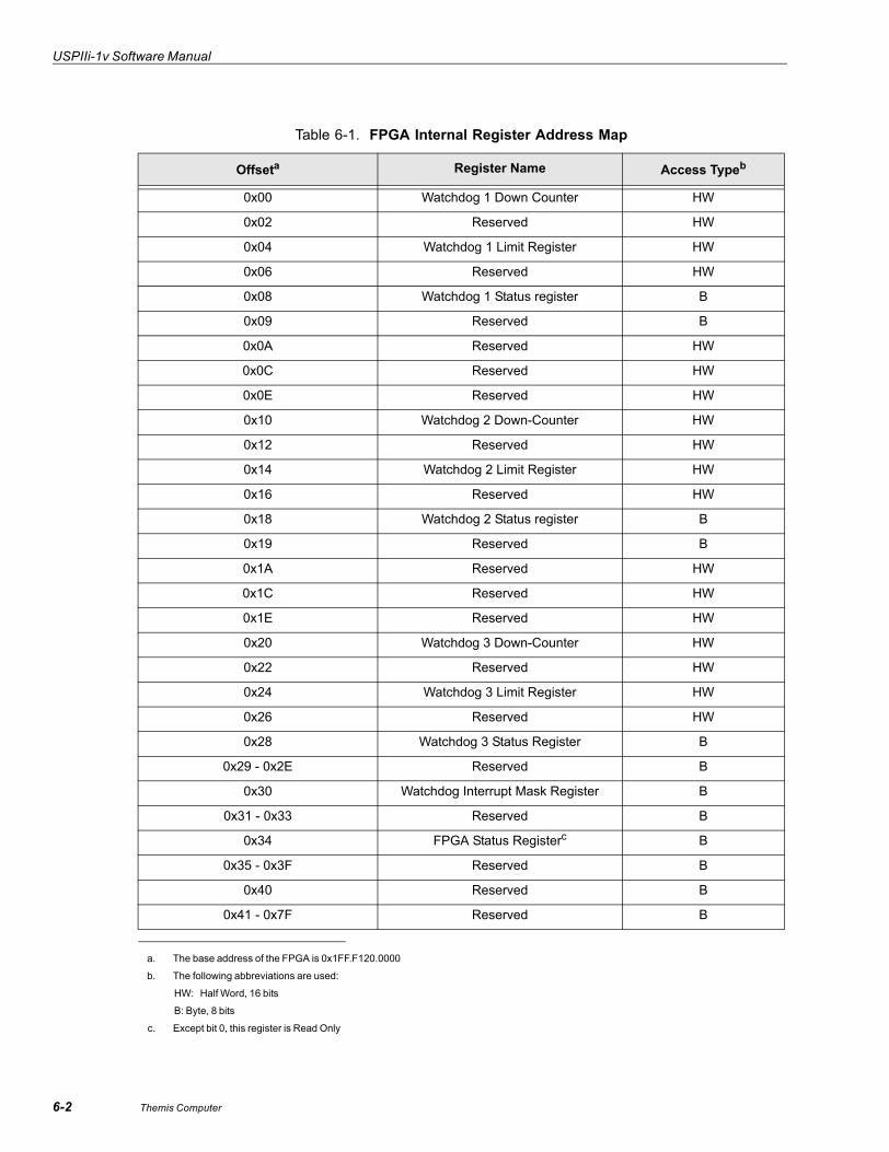
USPIIi-1v Software Manual
Table 6-1. FPGA Internal Register Address Map
Offseta
a. The base address of the FPGA is 0x1FF.F120.0000
Register Name Access Typeb
b. The following abbreviations are used:
HW: Half Word, 16 bits
B: Byte, 8 bits
0x00 Watchdog 1 Down Counter HW
0x02 Reserved HW
0x04 Watchdog 1 Limit Register HW
0x06 Reserved HW
0x08 Watchdog 1 Status register B
0x09 Reserved B
0x0A Reserved HW
0x0C Reserved HW
0x0E Reserved HW
0x10 Watchdog 2 Down-Counter HW
0x12 Reserved HW
0x14 Watchdog 2 Limit Register HW
0x16 Reserved HW
0x18 Watchdog 2 Status register B
0x19 Reserved B
0x1A Reserved HW
0x1C Reserved HW
0x1E Reserved HW
0x20 Watchdog 3 Down-Counter HW
0x22 Reserved HW
0x24 Watchdog 3 Limit Register HW
0x26 Reserved HW
0x28 Watchdog 3 Status Register B
0x29 - 0x2E Reserved B
0x30 Watchdog Interrupt Mask Register B
0x31 - 0x33 Reserved B
0x34 FPGA Status Registerc
c. Except bit 0, this register is Read Only
B
0x35 - 0x3F Reserved B
0x40 Reserved B
0x41 - 0x7F Reserved B
6-2 Themis Computer

6. FPGA, Watchdog and Temperature Sensors Registers
6.1.2 FPGA Status Register
The physical address of this register is 0x1FF.F120.0034.
6.1.3 3-Level Watchdog Registers
When a watchdog is started the counter register is loaded with the contents of the limit register or when a readto the counter register occurs. Either action will cause the counter register to begin its countdown from theprogrammed limit to zero. A watchdog expires when its counter register has counted down to zero (0). Thehexadecimal offsets for these registers are provided in Table 6-1, "FPGA Internal Register Address Map." .Note that the software should never read the counter register before the limit register has first beenprogrammed. In this case, the (default) value of the limit register is 1 and the watchdog will expire on the next10 MHz clock cycle.
All watchdog status registers contain 2 read-only information bits:• Bit 0: the “Running Bit” indicates, when set to ‘1’, that the counter register has started its countdown at
least once. This bit is only reset when the watchdog itself is reset.• Bit 1: the “Expired Bit” indicates, when set to ‘1’ that the counter value is at zero (0) and the respective
watchdog has expired.
Caution — Since the EBus2 is little-endian, an odd byte access will start a watchdog. Any access to a 16-bit Watchdog register (Limit register or Counter register) must be made by half-word access.
Upon expiration, any high-order watchdog will reset a lower-order watchdog, i.e: The expiration of watchdog3 resets watchdog 1 and watchdog 2 to their initially programmed states.
Table 6-2. FPGA Status Register
Bits Description Status Access
0 USER_LED Bit ‘1’ if the USER LED is on. R/W
‘0’ if the USER LED is off
1 Reserved Reserved R0
2 ROMBO Select Bit. ‘0’: The system’s boot program is on the ROMBO Connector
R
‘1’: The systems’ boot program is on the Flash EPROM
3 Reserved Reserved R0
4 Reserved Reserved R0
5 Reserved Reserved R0
6 Functional Bit ‘0’: The USPIIi-1v’s power supply has been over 95% of the nominal value for at least 500 milliseconds.
R
‘1’: The USPIIi-1v’s power supply has been under 95% of the nominal value for at least 500 milliseconds.
7 XCLOCK_10MHz This pin mirrors the 10 MHz clock output. R0
Themis Computer 6-3
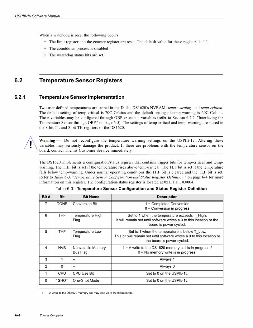
USPIIi-1v Software Manual
When a watchdog is reset the following occurs:• The limit register and the counter register are reset. The default value for these registers is ‘1’.• The countdown process is disabled• The watchdog status bits are set.
6.2 Temperature Sensor Registers
6.2.1 Temperature Sensor Implementation
Two user defined temperatures are stored in the Dallas DS1620’s NVRAM: temp-warning and temp-critical.The default setting of temp-critical is 70C Celsius and the default setting of temp-warning is 60C Celsius.These variables may be configured through OBP extension variables (refer to Section 6.2.2, "Interfacing theTemperature Sensor through OBP," on page 6-5). The settings of temp-critical and temp-warning are stored inthe 8-bit TL and 8-bit TH registers of the DS1620.
Warning —! Do not reconfigure the temperature warning settings on the USPIIi-1v. Altering thesevariables may seriously damage the product. If there are problems with the temperature sensor on theboard, contact Themis Customer Service immediately.
The DS1620 implements a configuration/status register that contains trigger bits for temp-critical and temp-warning. The THF bit is set if the temperature rises above temp-critical. The TLF bit is set if the temperaturefalls below temp-warning. Under normal operating conditions the THF bit is cleared and the TLF bit is set.Refer to Table 6-3, "Temperature Sensor Configuration and Status Register Definition," on page 6-4 for moreinformation on this register. The configuration/status register is located at 0x1FF.F110.0004.
Table 6-3. Temperature Sensor Configuration and Status Register Definition
Bit # Bit Bit Name Description
7 DONE Conversion BIt 1 = Completed Conversion0 = Conversion in progress
6 THF Temperature High Flag
Set to 1 when the temperature exceeds T_High.It will remain set until software writes a 0 to this location or the
board is power cycled.
5 THF Temperature Low Flag
Set to 1 when the temperature is below T_Low.This bit will remain set until software writes a 0 to this location or
the board is power cycled.
4 NVB Nonvolatile Memory Bus Flag
1 = A write to the DS1620 memory cell is in progress.a0 = No memory write is in progress.
a. A write to the DS1620 memory cell may take up to 10 milliseconds.
3 1 -- Always 1
2 0 -- Always 0
1 CPU CPU Use Bit Set to 0 on the USPIIi-1v.
0 1SHOT One-Shot Mode Set to 0 on the USPIIi-1v.
6-4 Themis Computer

6. FPGA, Watchdog and Temperature Sensors Registers
If the temperature of USPIIi-1v should raise above temp-critical the THF bit in the configuration and statusregister will be set to 1 and the temperature sensor will power the board down by shutting off the 1.9V and3.3 V DC-DC converters. Once the board temperature cools to a below temp-warning, a POR reset will beissued and the USPIIi-1v will resume operation. The THF bit in the configuration and status register willremain set through the board reset to allow software to detect the cause of the reset. The bit may be clearedby writing 0 to it or by cycling the power on the USPIIi-1v.
6.2.2 Interfacing the Temperature Sensor through OBP
The temperature sensor may be monitored and configured through the OBP. Two commands have beenimplemented to enable/disable the temperature monitoring after each boot.
mkm0 enables the temperature monitoring:
ok mkm0
Then, type [control-D][control-R] and reset the board. The temperature monitoring will be always enabledafter booting.
mkm1 disables the temperature monitoring:
ok mkm1
Then, type [control-D][control-R] and reset the board. The temperature monitoring will be always disabledafter booting. Display the banner to check for a trailing M after the version number.
ok banner
SPARCengine(tm)Ultra(tm) THEMIS-USPIIi-1v (UltraSPARC-IIi 300MHz), No keyboardOpenboot 3.10.27 Build.13M, 128 MB memory installed, Serial #4660.Ethernet address 0:80:b6:2:15:74, Host ID: 80001234
ok
OBP extension commands designed to interface with the Dallas DS1620 are presented in Table 6-4,"Temperature Sensor OBP Commands," on page 6-5.
Table 6-4. Temperature Sensor OBP Commands
Command Description
showT Reads and displays the temperature of the DS1620 in Celsius
wconfig writes to the configuration and status register
rconfig reads from the configuration and status register
clr-config clears the configuration and status register.
Themis Computer 6-5
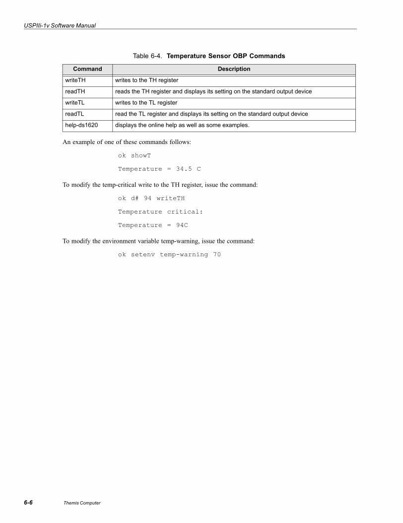
USPIIi-1v Software Manual
An example of one of these commands follows:
ok showT
Temperature = 34.5 C
To modify the temp-critical write to the TH register, issue the command:
ok d# 94 writeTH
Temperature critical:
Temperature = 94C
To modify the environment variable temp-warning, issue the command:
ok setenv temp-warning 70
writeTH writes to the TH register
readTH reads the TH register and displays its setting on the standard output device
writeTL writes to the TL register
readTL read the TL register and displays its setting on the standard output device
help-ds1620 displays the online help as well as some examples.
Table 6-4. Temperature Sensor OBP Commands
Command Description
6-6 Themis Computer

77Themis USPIIi-1V Software
7.1 Introduction
This chapter describes the software used on the Themis USPIIi-1V. This includes the OBP firmware, SunSolaris Operating system, and WIND RIVER Systems VxWorks Operating system. The default firmware isSun’s OBP (Open Boot Prom) that has been modified to support VME. OBP will boot the Solaris Operatingsystem. User’s can also install VxWorks bootrom firmware (bootrom.bin file). The VxWorks bootrom willboot the VxWorks image.
7.2 SUN OBP (Open Boot Prom)
The Themis USPIIi-1V OBP is based on OBP 3.10.x from SUN. Themis has added several OBP commandextensions that are specific to the USPIIi-1V. All other OBP commands are the same as the Sun UltraIIiPlatform. Specific details of the OBP architecture are defined in the IEEE 1275 specification document.Reference materials that describe the OBP include:
• OpenBoot 3.1 Command Reference -- Sun Part Number: 802-3242-31
• OpenBoot Quick Reference -- Sun Part Number: 802-5675-31
• Writing FCode 3.1 Programs -- Sun Part Number: 802-3239-31.f3f_
Themis Computer 7-1

USPIIi-1v Software Manual
7.2.1 Description of OBP VME Environment Variables
These variables may be set at the ok prompt in OBP by using the setenv command
ok setenv variable_name value
when running Solaris with the command (the syntax may vary depending on the shell used):
# eeprom variable_name=value
A board RESET is required for the new values to take effect.
Important: All values are decimal.
Table 7-1. OBP VME Environment Variables
Name Default Value Description
vme32-slave-base 0 Slave window address in A32 mode
vme24-slave-base 0 Slave window address in A24 mode
vme32-slave-size 8388608(0x800000) Slave window address in A32 mode
vme24-slave-size 1048576(0x100000) Slave window size in A24 mode
vme-irq-to-service VME Interrupt to be serviced by a VME leaf driver.
vme-bus-request-level 3 Level used to request VME
vme-arbitration-mode priority If Universe II is SYSCON: Arbitration mode used
vme-release-mode ror When the Universe II releases VME, it is going to use either ROR (release or
request) or RWD (release when done)
vme-request-mode demand When the Universe II requests the VME, it is going to use either demand or FAIR
mode
vme32-master-base 0 Defines a master window on VME. All subsequent VME mappings that fall
within this window wil use the same Uni-verse II master window
vme32-master-size 0 Size of the aforementionned master window. Needs to be less than 256MB.
temp-critical 70 Temperature threshold. See Chapter 6, "FPGA, Watchdog and Temperature
Sensors Registers,"
temp-warning 60 Temperature threshold. See Chapter 6, "FPGA, Watchdog and Temperature
Sensors Registers,"
7-2 Themis Computer
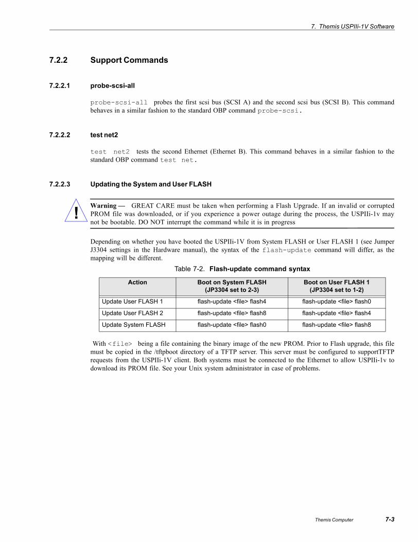
7. Themis USPIIi-1V Software
7.2.2 Support Commands
7.2.2.1 probe-scsi-all
probe-scsi-all probes the first scsi bus (SCSI A) and the second scsi bus (SCSI B). This commandbehaves in a similar fashion to the standard OBP command probe-scsi.
7.2.2.2 test net2
test net2 tests the second Ethernet (Ethernet B). This command behaves in a similar fashion to thestandard OBP command test net.
7.2.2.3 Updating the System and User FLASH
Warning —! GREAT CARE must be taken when performing a Flash Upgrade. If an invalid or corruptedPROM file was downloaded, or if you experience a power outage during the process, the USPIIi-1v maynot be bootable. DO NOT interrupt the command while it is in progress
Depending on whether you have booted the USPIIi-1V from System FLASH or User FLASH 1 (see JumperJ3304 settings in the Hardware manual), the syntax of the flash-update command will differ, as themapping will be different.
With <file> being a file containing the binary image of the new PROM. Prior to Flash upgrade, this filemust be copied in the /tftpboot directory of a TFTP server. This server must be configured to supportTFTPrequests from the USPIIi-1V client. Both systems must be connected to the Ethernet to allow USPIIi-1v todownload its PROM file. See your Unix system administrator in case of problems.
Table 7-2. Flash-update command syntax
Action Boot on System FLASH(JP3304 set to 2-3)
Boot on User FLASH 1(JP3304 set to 1-2)
Update User FLASH 1 flash-update <file> flash4 flash-update <file> flash0
Update User FLASH 2 flash-update <file> flash8 flash-update <file> flash4
Update System FLASH flash-update <file> flash0 flash-update <file> flash8
Themis Computer 7-3

USPIIi-1v Software Manual
7.2.3 Additional OBP commands
Below is a list of OBP commands that have been added to OBP for the USPIIi-1V:
7.2.3.1 Accessing VME from OBP
Prior to actually accessing VME from OBP, the user needs to make sure that the UNIVERSE II PCI targetimages are set correctly. A PCI target image is actually a window from PCI Bus to VMEbus. Each image orwindow defines a contiguous range of PCI addresses (base address and size).When a PCI cycle is issued bythe USPIIi CPU with an address falling inside a particular window address range, the UNIVERSE II willpropagate that cycle to the VME. The VME cycle will be formed according to the attributes defined in thewindow registers:
• VME address
• VME Address modifier
• ...
(Please refer to the UNIVERSE II user's manual for details). The Themis OBP command "show-universe-regs" can be used to visualize the settings of the 8 windows. Each window is controlled by 4 UNIVERSE IIregisters:
• LSx_CTL : control register.
Table 7-3. Additional OBP Commands
Command Description
show-universe-regs Reads and displays all the UNIVERSE II registers
<offset> universe-reg@ Reads and place on the OBP stack, the UNIVERSE II register content located at offset <offset> from the UNIVERSE II base address
<offset> universe-reg@ . Reads and displays the UNIVERSE II register content located at offset <offset> from the UNIVERSE II base address
<data> <offset> universe-reg! Writes the value <data> in the UNIVERSE II register located at offset <offset> from the UNIVERSE II base address
showT Reads and displays the temperature of the DS1620 in Celsius
wconfig writes to the configuration and status register
rconfig reads from the configuration and status register
clr-config clears the configuration and status register.
writeTH writes to the TH register
readTH reads the TH register and displays its setting on the standard output device
writeTL writes to the TL register
readTL read the TL register and displays its setting on the standard output device
help-ds1620 displays the on-line help as well as some examples.
7-4 Themis Computer

7. Themis USPIIi-1V Software
• LSx_CTL: PCI base address of the window.
• LSx_CTL: PCI bound address of the window.
• LSx_CTL: Translation register.
Suppose we want to access VME A32:0xaa00.0000:
ok setenv vme32-master-base 0xaa00.0000ok setenv vme32-master-size 0x1000.0000ok reset.....ok show-universe-regs
This command will tell us that the mapping we defined using the “vme32-master-base" and "vme32-master-size" THEMIS OBP variables are is controlled by the 7th window (LS7_CTL, LS7_BS, LS7_BD, LS7_TO).The LS7_BS register contains the base PCI address of that window (should be 0x800.0000). Now we canaccess VME using the OBP " space " command, which permits us to use physical addresses by bypassing theCPU MMU:
ok 1234 1ff.0800.0000 15 spacel! (writes 1234 to VME address A32:0xaa0.0000)ok 1ff.0800.0000 15 spacel? (reads back from that address)
0x1ff.0000.0000 is the base address of the PCI bus through which VME is accessed. 0x15 is the SPARC ASI(address space identifier) that is defined for PCI accesses.
Note —The above VME accesses were made using the 0x09 Address modifier code. This could be a problem in accessing other VME boards (like the Themis 1V, since it is programmed to accept user address modifiers-even though this can be changed). To set the address modifier to be 0x0d (supervisor), simply do:
ok 1dc universe-reg@ 1000 or 1dc universe-reg!
This will set the SUPER bit in LSI7_CTL. That was for A32 VME accesses. These accesses are done using the 8 PCI target image windows.
For A24 and A16 accesses a special UNIVERSEII window is being used : The special PCI target image.The mechanism is the same as for A32 accesses. Please refer to the UNIVERSE II user's manual fordetails.
Themis Computer 7-5
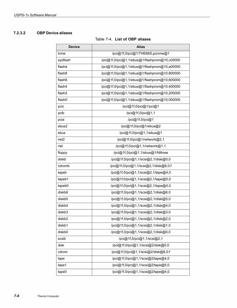
USPIIi-1v Software Manual
7.2.3.2 OBP Device aliasesTable 7-4. List of OBP aliases
Device Alias
tvme /pci@1f,0/pci@1/THEMIS,pcivme@1
sysflash /pci@1f,0/pci@1,1/ebus@1/flashprom@10,c00000
flasha /pci@1f,0/pci@1,1/ebus@1/flashprom@10,a00000
flash8 /pci@1f,0/pci@1,1/ebus@1/flashprom@10,800000
flash6 /pci@1f,0/pci@1,1/ebus@1/flashprom@10,600000
flash4 /pci@1f,0/pci@1,1/ebus@1/flashprom@10,400000
flash2 /pci@1f,0/pci@1,1/ebus@1/flashprom@10,200000
flash0 /pci@1f,0/pci@1,1/ebus@1/flashprom@10,000000
pcic /pci@1f,0/pci@1/pci@1
pcib /pci@1f,0/pci@1,1
pcia /pci@1f,0/pci@1
ebus2 /pci@1f,0/pci@1/ebus@2
ebus /pci@1f,0/pci@1,1/ebus@1
net2 /pci@1f,0/pci@1/network@2,1
net /pci@1f,0/pci@1,1/network@1,1
floppy /pci@1f,0/pci@1,1/ebus@1/fdthree
diskb /pci@1f,0/pci@1,1/scsi@2,1/disk@0,0
cdromb /pci@1f,0/pci@1,1/scsi@2,1/disk@6,0:f
tapeb /pci@1f,0/pci@1,1/scsi@2,1/tape@4,0
tapeb1 /pci@1f,0/pci@1,1/scsi@2,1/tape@5,0
tapeb0 /pci@1f,0/pci@1,1/scsi@2,1/tape@4,0
diskb6 /pci@1f,0/pci@1,1/scsi@2,1/disk@6,0
diskb5 /pci@1f,0/pci@1,1/scsi@2,1/disk@5,0
diskb4 /pci@1f,0/pci@1,1/scsi@2,1/disk@4,0
diskb3 /pci@1f,0/pci@1,1/scsi@2,1/disk@3,0
diskb2 /pci@1f,0/pci@1,1/scsi@2,1/disk@2,0
diskb1 /pci@1f,0/pci@1,1/scsi@2,1/disk@1,0
diskb0 /pci@1f,0/pci@1,1/scsi@2,1/disk@0,0
scsib /pci@1f,0/pci@1,1/scsi@2,1
disk /pci@1f,0/pci@1,1/scsi@2/disk@0,0
cdrom /pci@1f,0/pci@1,1/scsi@2/disk@6,0:f
tape /pci@1f,0/pci@1,1/scsi@2/tape@4,0
tape1 /pci@1f,0/pci@1,1/scsi@2/tape@5,0
tape0 /pci@1f,0/pci@1,1/scsi@2/tape@4,0
7-6 Themis Computer

7. Themis USPIIi-1V Software
7.3 VxWorks Firmware
The VxWorks firmware is generated by the following command run on a system that has been loaded with theTornado environment, the UltraSPARC ODL (Object Development Library) from Wind River Systems, andthe Themis BSP (board support package) for the USPIIi-1V.
$ cd <VxWorks HOME DIRECTORY>/target/config/tsIIi1v$ make bootrom.bin
Then the file bootrom.bin needs to be placed on a tftp server, just like for updating the FLASH with OBP.
7.4 SUN Solaris
The USPIIi-1V can run the Solaris OS from either a local disk or from the Ethernet network as a disklessclient. In the case of a local disk, the Solaris OS will be loaded out of the Sun Solaris CD-ROM. To install theUSPIIi1v as a diskless, users need to run Sun’s Solstice on a boot server system. Please refer to Sun’sdocumentation on how to install the Solaris Operating System.
In order to be able to access VME, from Solaris, users need to install the Themis VME Nexus driver for theUSPIIi-1V. The VME Nexus driver is a Solaris package, that is installed/removed using the pkgadd(1M)/pkgrm(1M) Solaris command. The installation is menu driven, and users should always reboot the systemin the reconfiguration mode (boot -r) right after installing the VME Nexus driver.
disk6 /pci@1f,0/pci@1,1/scsi@2/disk@6,0
disk5 /pci@1f,0/pci@1,1/scsi@2/disk@5,0
disk4 /pci@1f,0/pci@1,1/scsi@2/disk@4,0
disk3 /pci@1f,0/pci@1,1/scsi@2/disk@3,0
disk2 /pci@1f,0/pci@1,1/scsi@2/disk@2,0
disk1 /pci@1f,0/pci@1,1/scsi@2/disk@1,0
disk0 /pci@1f,0/pci@1,1/scsi@2/disk@0,0
scsi /pci@1f,0/pci@1,1/scsi@2
ttyb /pci@1f,0/pci@1,1/ebus@1/su@14,3602f8
ttya /pci@1f,0/pci@1,1/ebus@1/su@14,3803f8
ttyd /pci@1f,0/pci@1,1/ebus@1/se@14,400000:b
ttyc /pci@1f,0/pci@1,1/ebus@1/se@14,400000:a
Table 7-4. List of OBP aliases
Device Alias
Themis Computer 7-7

USPIIi-1v Software Manual
7.4.1 Installing the USPIIi-1V VME Nexus driver
The software interface for USPIIi-1V is distributed as a software package for Solaris 2.x systems. Thesoftware package is named THEMISvme and can be installed and removed like other standard Solarissoftware packages, by using the pkgadd and pkgrm commands.
7.4.1.1 Installing THEMISvme
The THEMISvme package is distributed on standard media and can be installed directly from the media. Toinstall the package, place the installation media in the appropriate slot and execute this command:
# pkgadd -d <media name>
where <media name> is the name of the media on your system. The pkgadd command will copy thecontents of the package to the appropriate directories and perform the necessary installation. After thecommand completes, the system has to be rebooted for the new software to be operational.The user maychoose to install these drivers by executing a script provided for that purpose. The sample drivers are notrequired for the normal operation of the USPIIi-1V system
7.4.2 Sample VME Programs and VME leaf drivers
The software interface provided for the USPIIi-1V platform fully supports standard VMEbus device driverswritten for Solaris environments. It is the intention of Themis Computer to fully support users who wish towrite their own VME device drivers that would function on USPIIi-1V platforms. To aid these users and toillustrate the specific features of the VMEbus architecture, Themis provides a number of sample devicedrivers. Themis provides the complete source code and the necessary configuration files for these drivers. Thedrivers are located under the /opt/THEMISvme directory.
• vmeintr: is a sample driver provided by Themis Computer to illustrate the vectored interrupt mechanism ofthe VMEbus. The vmeintr driver relies on the driver configuration files to specify the interrupts it shouldhandle. Each instance of the driver registers the interrupts with the system. Through the ioctls implemented bythe driver, the user can generate interrupts and send them to the appropriate driver instances. The interruptgenerator and the interrupt receiver need to run on different computers.
• vmedvma: is a sample driver provided by Themis Computer to illustrate the use of Direct Virtual MemoryAccess within a device driver. The user can ask the driver to allocate a DMA region on the VMEbus. Thedriver allocates all the necessary resources to support a DVMA transfer to this region. The driver alsoimplements mechanisms by which the user program can write to or read from the DVMA region.
Furthermore, the VME NEXUS package includes example programs, to help users build their own applicationor test VME. The programs are:
• dmatest: This program is making use of the UNIVERSE II DMA engine. Several options areavailable that are selected by command line parameters.
• vme_dvma: This program is setting the USPIIi-1V to be accessible from VME by enabling aslave window.
• vme_intr: This program is using the example driver vmeintr to send/receive VME interrupts.
7-8 Themis Computer
7. Themis USPIIi-1V Software
• vme_mmap: this program accesses VME using the Solaris mmap(2) system calls. The systemcalls works by programming the MMU to map VME memory within the address space of thecalling program. Further VME accesses are done using simple references, like C languagepointers.
• vme_rw: This program accesses VME using the more traditionnal UNIX approach of doing I/Os.VME memory is accessed using the UNIX read(2) and write(2) system calls. This will result inslower VME transfer speed.
Themis Computer 7-9

USPIIi-1v Software Manual
7-10 Themis Computer


