151
CONTENTS
Advanced Measures for Environmental Conservation as Management Policy........................................................... 2
LCD Modules ....................................................................... 8
EL Display Modules.............................................................. 14
CMOS IMAGE SENSORS
CMOS Camera Modules ...................................................... 15
CCDs
Higher-resolution CCDs ....................................................... 161/3-type CCDs...................................................................... 161/3.8-type CCD .................................................................... 171/4-type CCDs...................................................................... 171/3-type CCDs with Dual-power-supply (5 V/12 V) Operation ............................................................................. 17CCD Peripheral ICs/LSIs...................................................... 18
LSIs FOR LCDs/ANALOG ICs
For Notebook PCs, PC Monitors and LCD TVs.................... 25For Mobile Equipment .......................................................... 26For Mobile Phones ............................................................... 27Peripheral ICs for LSIs for LCDs .......................................... 29
SYSTEM LSIs
Special-function LSIs ........................................................... 31IPs ........................................................................................ 32
SMART CARD SYSTEMS
Smart Cards/LSI Modules for Smart Cards ......................... 33Reader/Writer for Smart Cards ............................................ 34SDK (Software Development Kit) for Smart Cards............... 34
FLASH MEMORIES AND COMBINATION MEMORIES
FLASH MEMORIES
............................................................. 35
SYSTEM-FLASH
................................................................. 36
HIGHLY FUNCTIONAL FLASH MEMORIES
Boot Block Type 3 V Page Mode Flash Memories................ 38
STANDARD FLASH MEMORIES
Boot Block Type 3 V Flash Memories................................... 38
SYSTEM-FLASH
Fast-Reprogramming System-Flash for Digital Equipment .. 39System-Flash for Amusement Products............................... 39System-Flash for Automotive Use........................................ 40System-Flash for Network Equipment.................................. 40
COMBINATION MEMORIES
Boot Block Type Flash Memory + Pseudo SRAM ................ 41
POWER DEVICES/ANALOG ICs
Low Power-Loss Voltage Regulators.................................... 42Surface Mount Type Low Power-Loss Voltage Regulators ... 44Surface Mount Type Chopper Regulators (DC-DC Converters)............................................................. 48Chopper Regulators (DC-DC Converters) ........................... 49Power Supply ICs for CCDs/CCD Camera Modules ............ 50Power Supply ICs for TFT-LCDs........................................... 50Fail Safe IC........................................................................... 51LED Drivers.......................................................................... 51Laser Diode Drivers ............................................................. 52
ANALOG ICs
Video Interface ICs for TFT-LCDs......................................... 53Power Amplifiers for Wireless LAN....................................... 53ICs for Audio Equipment ...................................................... 54
TFTSTN CG SiliconCSTN
EL
LSI REG
PACKAGES
CSP (Chip Size Package)..................................................... 55LGA (Land Grid Array Package) ........................................... 56SiP (System in Package) ...................................................... 57SOF (System On Film) ......................................................... 59Package Lineup .................................................................... 60
OPTOELECTRONICS
Photocoupler Index Tree
.................................................... 67
Photocouplers
Phototransistor Output....................................................... 68 OPIC Output ...................................................................... 72
Phototriac Coupler Index Tree
........................................... 75Phototriac Couplers .............................................................. 76
Solid State Relay Index Tree
.............................................. 78Solid State Relays ................................................................ 79
Photointerrupter Index Tree
............................................... 82Photointerrupters <Transmissive type> ................................ 83 Single Phototransistor Output............................................ 83 Darlinton Phototransistor Output ....................................... 85 OPIC Output ...................................................................... 85Photointerrupters <Reflective type> ..................................... 87 Single Phototransistor Output............................................ 87 Darlinton Phototransistor Output ....................................... 88 OPIC Output ...................................................................... 88Photointerrupters for Specific Applications........................... 89 Transmissive Type.............................................................. 89 Reflective Type................................................................... 91
Phototransistor Index Tree
................................................. 92Phototransistors.................................................................... 93
Photodiodes/OPIC Light Detectors
PIN Photodiodes................................................................... 94PSD (Position Sensitive Detector) ........................................ 94Blue Sensitive Photodiodes.................................................. 94Laser Power Monitoring Photodiodes for Optical Disc System ........................................................ 95RGB Color Sensor................................................................ 95Ambient Light Sensors ......................................................... 95
Infrared Emitting Diode Index Tree
.................................... 100Infrared Emitting Diodes ....................................................... 101
Optical-Electric Sensor Index Tree
.................................... 102Distance Measuring Sensor Lineup...................................... 102Wide Angle Sensor Lineup ................................................... 102High-Precision Displacement Sensor ................................... 102Paper Size Sensor Lineup .................................................... 102Dust Sensor Unit Lineup....................................................... 102Color Toner Concentration (Deposition Amount) Sensor Lineup................................................................................... 102Distance Measuring Sensors................................................ 103Wide Angle Sensors ............................................................. 104Paper Size Sensors .............................................................. 105High-Precision Displacement Sensor ................................... 106Dust Sensor Units................................................................. 106Color Toner Concentration (Deposition Amount) Sensors.... 106
Fiber Optics Index Tree
...................................................... 107Fiber Optics Lineup for Audio Equipment ............................. 107
OPTO

LCD
ICOp
toel
ectr
onic
s LE
D /
Lase
r Di
ode
RF C
ompo
nent
IR
Dev
ice
Devi
ce fo
r Op
tical
Dis
cs
Transmission/Reception Devices for MOST Compatible Optical Fiber......................................................................... 107Fiber Optic Transmitters ....................................................... 108Fiber Optic Receivers........................................................... 109Optical Transmission Device ................................................ 110Optical Reception Device..................................................... 110
LED
High-Luminosity LED Lamps................................................ 111LED Lamps .......................................................................... 113Dichromatic LED Lamps ...................................................... 115High-Luminosity Chip LEDs ................................................. 116Chip LEDs ............................................................................ 117High-Luminosity Dichromatic Type Chip LEDs..................... 117Dichromatic Type Chip LEDs................................................ 118High-Luminosity White Type Chip LEDs............................... 118Pastel Color Chip LEDs........................................................ 118High-Luminosity Dichromatic Type Chip LEDs (RGB 3-color) ....................................................................... 119LEDs for Camera Data Back ................................................ 119
LASER DIODE
Laser Diodes ........................................................................ 120
RF COMPONENTS
Low Noise Blockdown ConverterEurope: LNB for Broadcasting Satellite ................................ 121U.S.A.: LNB for FSS Broadcast/(Others: LNB for Communication) ................................................................... 121Japan/Asia/Australia: LNBs for CS Digital Satellite Broadcast ............................................................................. 122Japan: LNBs for BS/CS 110° Satellite Broadcast................. 122Digital DBS Front-End Units................................................. 123QPSK Demodulator Circuit Built-in Type .............................. 1248 PSK Demodulator Circuit Built-in Type.............................. 124Combination Front-End for Digital Terrestrial and Digital Satellite Broadcasting .......................................................... 125Digital Terrestrial Front-End Unit .......................................... 126Front-End Units for ISDB-T/DVB-T....................................... 126
LED
LASER
RF
Two-In-One RF Units ............................................................ 127Analog Terrestrial RF Front-End Unit.................................... 128RF Front-End Units............................................................... 1281-Segment Digital Terrestrial Module.................................... 1291-segment/3-segment Digital Terrestrial Module .................. 129USB Interface Wireless LAN Module.................................... 130
IR DEVICE
Infrared Data Communication Device Index Tree
............ 131Infrared Data Communication Devices ................................. 132Infrared Wireless Audio Transmission Device....................... 133
IR Detecting Unit for Remote Control Index Tree
............. 134IR Detecting Units for Remote Control ................................. 135
Switching Power Supplies (Custom)..................................... 137Switching Power Supply with Integrated High/Low Voltage Circuit (Custom).................................................................... 137
PRINTED CIRCUIT BOARD
Advanced Flex Printed Circuit Boards .................................. 138Flexible Build-up Multilayer PCBs......................................... 139Flexible Printed Circuit Boards ............................................. 140
PICKUP
Slim Combo Drive Pickup..................................................... 141Slim DVD-ROM Drive Pickup................................................ 141DVD Pickup for Automotive Use ........................................... 141
IR
POWER
PCB
UNIT
INDEX
................................................................................ 142
NOTICE
.............................................................................. 143

1. To Conserve the Environment:
The Sharp Group will fulfill our responsibility for environmental conservation by promoting the creation of proprietary technologies that contribute to protection of the global environment, and by carrying out
our product development and business activities in an environmentally conscious manner.
2. To Develop Environmentally Conscious Products and Services, and Conduct Our Business Operations in an Environmentally Conscious Manner:
Creating an Environmentally Conscious Company with Sincerity and Creativity
Contribution to Conservation of the Global Environment
Contribution to Conservation of the Global Environment
Basic Environmental Philosophy
The Sharp Group Charter of Corporate Behavior
The Sharp Code of Conduct
We will comply with all applicable environmental laws, regulations and territorial agreements, and work to practice efficient use and conservation of resources and energy voluntarily, in the recognition that environmental conservation is an essential facet of corporate and individual pursuits.
We will ensure proper use and control of chemical substances in our business activities including research, development and manufacturing, meeting or exceeding levels determined by laws and regulations.
We will engage in the active acquisition, reporting and promotion of environmental information at an international level, as the Sharp Group companies promote communication with shareholders and local residents.
We understand the importance of internal company systems and related details in acquiring third-party certification and recertification of our ISO environmental management systems, and we will conduct our business operations in accordance with relevant internal guidelines.
1
2
3
4
We will engage positively in the minimization of resource use, reduction in the size and weight of products, use of recycled materials, and the development of long-lasting, energy-saving, energy-creating products.
We will work to compile information related to harmful substances that might damage the environment or human health, and will not, as a matter of principle, make use of these harmful substances in our products, services and business activities.
We will use recyclable materials wherever possible, with product development focused as a matter of policy on structures that are detachable or capable of dismantling, and suited to recycling.
We will work aggressively to reduce greenhouse gas emissions in the full range of our business activities, in order to contribute to the prevention of global warming.
We will work to conduct our business in such a way to select and purchase materials that are harmless to the global environment, and to local residents and employees, for the resources needed for business activities (equipment, raw materials, subsidiary materials, tools, etc.).
We realize that waste material is a valuable resource, and we will actively conduct our business operations in such a way as to maximize the 3Rs (reduce, recycle and reuse) and will contribute to minimizing the amount of waste sent for permanent landfill disposal.
1
2
3
4
5
6
* The Sharp Group Charter of Corporate Behavior and the Sharp Code of Conduct were instituted in May 2005 as a revised edition of the preceding Sharp Charter of Conduct (instituted in 2003). The section above is an excerpt from descriptions of Sharp's environmental conservation efforts.For more information: http://sharp-world.com/corporate/eco/report/index.html
Advanced Measures for Environmental Conservation
In accordance with environmental guidelines established under Sharp’s Basic Environmental Philosophy, the Sharp Group Charter of Corporate Behavior, and the Sharp Code of Conduct, Sharp is pursuing environmental conservation in all aspects of its business activities. Since fiscal 2004, when the medium-term brand objective of becoming an environmentally advanced company was first set, Sharp has been promoting the Super Green Strategy to achieve its corporate vision and to establish sustainable manufacturing systems.
2

as Management Policy
Super Green Strategies to Become an Environmentally Advanced Company
Corporate Vision of Achieving “Zero Global Warming Impact by 2010”
SGP/DSuper Green Products and DevicesCreating products and devices with highenvironmental performance
SGMSuper Green ManagementEnhancing environmental sustainability management
SGTSuper Green TechnologiesDeveloping unique environmental technologiesthat contribute to environmental conservation
SGRSuper Green RecyclingRecycling used products to promoteresource recycling SGF
Super Green FactoriesFactories with high environmental consciousnessand trust from communities
SGT
SGM
SGP/D
SGR SGF
Sharp will limit to the greatest extent possible the amount of the greenhouse gas emissions resulting from its business activities around the world, while at the same time, significantly help reduce greenhouse gas emissions based on the energy-creating effects of solar cells and the energy-saving effects of products. The idea is for the amount of greenhouse gas emissions reduced to exceed the amount emitted by fiscal 2010.Sharp’s greenhouse gas emissions in fiscal 2006 were approximately 1.73 million t-CO2. At the same time, it is estimated that the solar cells Sharp produced over the 20 years up to fiscal 2005 generated approximately 1,322 GWh*1 in fiscal 2006. This is equivalent to a reduction in greenhouse gas emissions of approximately 0.56 million t-CO2
*2
*1 Calculation based on 844 MW, Sharp's total solar cell production over 20 years from 1986 to 2005.
*2 Calculated using a CO2 emission unit of 0.425 kg/kWh (fiscal 2005) at the receiving end, announced by the Federation of Electric Power Companies of Japan.
Reduce greenhouse gas emissions from
worldwide business activities
Boost the level ofreductions in greenhouse
gas emissions from energycreated by solar cells
and energy savedby products
3

Becoming an Environmentally Advanced Company—
Developing Super Green Technologies
Development of Green Devices and Super Green Devices
Energysaving
Recyclability Use standard plastic or materials that are easy to separateand disassemble (target: LCD devices)
Reduce total power consumption and reduce power consumedin standby mode compared to previous models
Greenmaterial
Control usage of chemical substances contained in parts andmaterials and use no substances prohibited under Sharp standards
Long life Extend the life of the product with exchangeable partsand consumables (target: LCD devices)
Resourcesaving Reduce weight or volume compared to previous models
Informationdisclosure
Provide information on chemical substances
Packaging Reduce packaging materials
Sharp calls its environmentally conscious devices “Green Devices.” To define criteria for development and design based on seven concepts such as low energy consumption and recyclability, Sharp established the Green Device Guidelines, which it began applying in fiscal 2004. In fiscal 2005, Sharp began certifying Green Devices that attain the highest possible levels of environmental performance as “Super Green Devices.”The development of Green Devices begins at the planning and designing stage, where every aspect of the product’s environmental impact is discussed. Sharp then sets specific objectives based on the Green Device Standard Sheet. Finally, in the trial manufacture and mass production stages, Sharp determines how well the actual product has met its objectives.In fiscal 2006, both Green Devices and Super Green Devices exceeded their sales ratio targets. In the coming years, Sharp plans to raise these figures even higher.
*1 Certification criteria for Green Devices and Super Green Devices in fiscal 2006: Green Devices had to satisfy at least 90% or more of all 20 assessment items (9 of which are compulsory) listed in the Environmental Performance Criteria. Super Green Devices will have to satisfy at least 95% or more the 20 assessment items (10 of which are compulsory) listed in the Environmental Performance Criteria. At the same time, they must be either the industry's No.1, or the industry's first devices in at least one item of the External Environmental Claim Standards.
To achieve Sharp’s corporate vision of becoming a company that has “zero global warming impact by 2010,” the development of superior environmental technologies is an essential factor in the environmental performance of products and devices and the reduction of environmental impact during production. Sharp conducts research and development in four areas of environmental technology: reduction of CO2 emissions, effective use of resources, elimination of use of harmful substances, and promotion of health and cleanliness.Sharp recognizes the most important technologies in these areas as one-of-a kindenvironmental technologies-key technologies for achieving global environmental conservation-and develops them under a company-wide development strategy.These technologies enhance environmental performance of products and devices, reduce environmental impact at plants, and facilitate recycling. Unique technologies, evolving from these developments, are what Sharp calls Super Green Technologies.
CO2 emission reductions(Energy creation, energy saving)
Effective use of resources(Reduce, reuse, recycle)
Elimination ofharmful substances Health, cleanliness
One-of-a-KindEnvironmentalTechnologies
Technologies that have no impact on global warming
One-of-a-Kind environmental technological development fields that give birth to Super Green Technologies
The Green Device concept
Technologies that contribute to environmental conservation
4

Super Green Technologies, Devices and Factories
Achievement of a Super Green Factory
Certification of Green Factories and Super Green Factories
Sharp is systematically acting to enhance the environmental consciousness of its production sites worldwide. Sharp has established proprietary assessment standards to rank factories with high environmental consciousness as Green Factories, and those with extremely high environmental consciousness as Super Green Factories, Sharp is planning to convert all its production sites around the world into Green Factories or higher by fiscal 2007.
Quantified environmental performance criteria are used to assess and approve a plant for certification. A plant must score 70 or more points out of a possible 100 in the assessment process to earn Green Factory certification, while scoring 90 or more points will result in Super Green Factory certification.Plans call for turning all Sharp Corporation production sites in Japan into Super Green Factories and all production sites in the Sharp Group to Green Factories or higher by the end of fiscal 2007.In fiscal 2006, three domestic bases and two overseas bases achieved Super Green Factory status, while a total of 10 bases in Japan and overseas earned Green Factory certification.
The Green Factory concept
Process required to achieve Super Green Factories
Information disclosure
Environmental consciousness
Greenhouse gases
Minimize emission of greenhouse gases
Energy Minimize energy consumption
Resources Minimize resource consumption
Atmosphere, water, soil
Minimize environmental burden on the atmosphere, water and soil
Harmony with the community
Encourage harmony with the local community
Disclose information on the environment
High environmental awareness among employees
Harmony with nature
Endeavor to preserve nature both on and off site
Chemical substances
Minimize risk of environmental pollution and accidents caused by chemical substances
Waste Minimize discharge of waste
90 points or more90 points or more
New factories Existing factories
Green Factory Concept
Super Green Factory
Assessments based on 21 quantified environmental performance criteria
Approach based on environmental impact assessments
Super Green Factory Green Factory
70 points or more
The plant's environmental performance is assessed from an objective third-party point of view and performance is defined for each item
based on the assessment results
5

From “Green” Factories to “Super Green” FactoriesSharp’s First Super Green Factory Kameyama Plant
Mie Plant Becomes First Existing Factory to Achieve Super Green Status
Participation in Local Environmental ActivitiesThe Mie Plant is actively involved in mitigating the impact of the plant on the surrounding environment, and is also engaged in local environmental preservation activities focused on the area’s mountains, rivers, and roads. We have received acclaim from local people for our participation in these activities, including the upkeep of the local forest as a water source, the maintenance of the neighboring forests and mountains, the cleaning of the Sanagawa River as the plant’s effluent stream, and the planting of flowers on National Route 42.
CO2 Emissions Reduced through PV Power System InstallationThe Mie Plant No. 3 installed a 180-kW photovoltaic power system on its south exterior wall. The system began generating electricity in March 2005. Used mainly to provide lighting for all non-manufacturing rooms, the system generated 141,000 kWh of power in 2006 and contributed to the reduction of about 60 tons of CO2 emissions.
The results described above are major efforts in upgrading to a Super Green Factory.
Mobile Liquid Crystal Display Groups(Taki, Mie Prefecture)
Participation in Environmental Education Programs at Local SchoolsAs part of our community outreach program, we have been cooperating with eight local schools in the town of Taki (one senior high, two junior high, and five elementary schools) on various educational projects, including factory tours, classes taught by visiting lecturers, and joint environmental activities.
Energy-Saving EffortsSince its completion, the Mie Plant has been strongly focused on energy conservation. In fiscal 2006 our efforts were recognized with an Agency for Natural Resources and Energy Director-General Prize for energy-efficient plant management. In addition, three members of the Mie Environmental Safety Promotion Center, who have been engaged in energy-saving efforts for many years, received prizes in recognition of their achievements in energy management. These awards are a testament to Sharp’s energy management and energy-saving efforts.
Waste Reduction EffortsIn 2004, we achieved zero discharge to landfill, eliminating waste by recycling all possible waste materials. Efforts are being made to further reduce emission of waste products by expanding the sale of valuable materials for reuse.
Fluoric Acid Effluent Recycling System Honored at 2004 WASTEC AwardThe Mie Plant No. 3 uses fluoric acid in its continuous grain silicon production process. The plant developed this system and has been using it since 2004 to recover and recycle the fluoric acid effluent. This system was recognized for its excellence and won the Business Activity Category Prize at the 2004 WASTEC (Waste Control and Recycling Technology Exhibition) Awards in Japan in November 2004. Prior to the introduction of this system, the fluoric acid from the effluent was used to make cement. Now it can be used repeatedly at the production site, while the distilled water from the effluent can be used as pure water.
Countering Global Warming by Unifying Diverse Power Sources Distributed over a Wide AreaThe Kameyama plant generates one-third of its annual electricity consumption and has reduced CO2 emissions to about 40% lower than previous levels by means of a cogeneration system* using liquefied natural gas (LNG) (approx. 26,400 kW), as well as one of the largest fuel cell systems in Japan (approx. 1,000 kW), and one of the world’s largest photovoltaic (PV) power generation systems (5,210 kW).
* Cogeneration system: A system designed to save energy by using city gas to generate electricity. The waste heat generated is then used in applications such as air conditioning, hot water supply and steam electricity generation.
AVC Liquid Crystal Display Group (Kameyama, Mie Prefecture)
An Efficient and Environment-Friendly Integrated Production SystemThe entire process is carried out in a single plant—from fabricating the LCD panels to final assembly. This system makes it possible to consolidate technical departments and strengthen our development capabilities, as well as shorten the lead-time from order to shipping. Eliminating the need to ship sub-assemblies between distant plants has also enabled us to slash the amount of packaging materials required for shipping and reduce emissions such as carbon dioxide (CO2).
Creating Energy at the Factory for Energy-Saving Products, Using One of the World’s Largest* PV Power Generation Systems In addition to the existing 60-kW photovoltaic (PV) power generation system, new PV power generation systems, in a total area of approx. 47,000 m2 and with a total output of 5,150 kW, have been installed. Located at the large-screen LCD TV factory, the distribution building, and on the roof and curtain wall of the Kameyama Plant No. 2, these systems generate an annual electricity output that would power 1,300 average Japanese households.
* As a building-installed system. Survey by Sharp.
Water Purifying System—100% Water Recycling in the Production ProcessThe plant collects all the wastewater from the production process of liquid crystal panels, etc. (max. 28,300 tons a day) and recycles it 100% with water purification techniques using microorganism treatment. Malodorous wastewater containing chemicals is deodorized using peat moss* from Ishikari River, Hokkaido.
* Bog moss decomposed and piled up for several thousands of years.
The Kameyama Plant Receives Japan Sustainable Management AwardThe Kameyama Plant in Japan was recognized for its outstanding environmental sustainability management by being chosen from among 125 applicants for the highest honor, the Sustainable Management Pearl Award, in the 2004 Japan Sustainable Management Awards* (sponsored by the Japan Sustainable Management Awards Committee and Mie Prefecture).This award shows the high esteem for the environmental measures—including 100% recycling of manufacturing process wastewater, the introduction of an LNG cogeneration system and the installation of a photovoltaic power system—taken by the Kameyama Plant, Sharp’s first Super Green Factory.The Kameyama Plant received the first Minister of Economy, Trade and Industry Award in the 8th Japan Water Prize (2006) and the Energy Saving Encouraging Prize in the 4th Excellent Cogeneration System Commendation (FY 2005) sponsored by the Japan Cogeneration Center.
* The Japan Sustainable Management Awards honor all organizations across the nation, no matter what their size or type of business—including private companies, NPOs and schools—that demonstrate outstanding results of their environmental sustainability management efforts.
The Kameyama Plant is Sharp's first “Super Green Factory”, a compilation of the company's environmental protection technologies.In preparing for construction, we gave a great deal of careful consideration to protecting the environment, beginning at the initial design stage. Working in consultation with local governments and with nearby residents, we carefully selected the parameters that would be subject to environmental protection measures. We chose the standards that would apply, and confirmed them through evaluation by independent experts.Also, when building the Kameyama Plant No. 2, we took the opportunity to introduce the latest environmental technology to make it one of the world’s most advanced “Super Green” factories.
6

* Sharp defines this as bringing the amount of buried waste (final disposal amount) as close to zero as to be negligible. In figures, a final disposal rate of less than 0.5% (final disposal rate = buried amount / total discharged amount x 100) is taken to be zero emissions.
ISO 14001 certification: September 24, 1996
Inauguration of a non-dilution nitrogen treatment plantThe Group built a new plant that uses the world’s first non-dilution treatment technology on the nitrogen contained in semiconductor plant wastewater. The technology combines “micro-nanobubble technology” with a unique microorganism treatment technology Sharp developed in June 2005. Operation of the plant began in July 2006.
Promotion of zero emissions*Zero emissions were achieved in 2001 through ongoing efforts such as in-house treatment of developing fluid by means of our own micro-organism treatment technology, reduction of the volume of process sludge produced, and recycling of waste into useful material.
Prevention of global warmingAn energy conservation committee has been formed to promote energy conservation efforts involving the entire Group. Efforts such as building a unique energy-saving outer air treatment system have been highly regarded, and the Group received a “2005 Excellent Energy Conservation Factory & Building (electricity category)” award from the Director-general of the Agency for Natural Resources and Energy.
Relations with the local communityIn August of each year, employees and their families and local people are invited to the “Family Day in Sharp (Summer Festival).” At this festival, an environmental exhibition space is prepared to provide an opportunity for people to experience nature and to introduce the environmental protection efforts of the facility.The plant also implemented the semiconductor industry's first full-scale risk communication (July 2005), and in cooperation with the local community, jointly produced a large communication panel (4 m x 6 m) called “Daimoncho—Yesterday and Today.” The panel is on display at our premises and is being used to introduce our business and Daimoncho to visitors. Communication activities such as these have been highly evaluated, and the Group received the “2005 PRTR Prize” sponsored by the Center for Environmental Information Science.
ISO 14001 certification: November 17, 2003Prevention of global warmingThe precise air-conditioning necessary for production activities is maintained by operating coolers and boilers on municipal gas, which produces little CO2. The turbo coolers provided in air-conditioning equipment use a waste heat recovery system. A remover optimized for greenhouse gases is provided to suppress emission of such gases and prevent global warming.
Promotion of zero emissions*Zero waste emission has been achieved through active efforts to reduce and reclaim waste, instituted from the beginning of the facility.Efforts to prevent pollutionAfter treatment at an in-house facility, all process waste water is discharged into the public sewer only after clearing voluntary standards stricter than waste water standards. Sludge produced in waste water treatment is sorted by type and reclaimed.Measures are taken such as installing equipment indoors to prevent noise escaping to the surrounding area from noisy equipment, such as large fans and large compressors. Noise levels at the site boundary are within regulation values.The plant is working to improve management of chemical substances, prevent accidents and environmental disasters, and reduce environmental impact.Efforts to contribute to the local communityThrough efforts such as inviting local people to festivals and activities to protect forests, the plant aims to deepen relations with people in the local area and protect the environment.Efforts are being made to beautify the area by participating in greenification activities in the Mihara Western Industrial District where this facility is located.Efforts are being made to issue a pamphlet introducing the facility and to disclose information. The pamphlet contains environmental activity records and other information.
ISO 14001 certification: June 25, 1996Prevention of water pollutionAll waste water from production processes and laboratories is purified at a waste water treatment station within the factory. Water is released into the sewer only after treatment based on voluntary standards stricter than environmental standards.Prevention of air pollutionWaste gases from acids and organic solvents produced by production processes and laboratories are purified with two types of waste gas treatment equipment, depending on the properties of the chemical substances. Eight acid scrubbers and 11 solvent scrubbers are installed on the roof of the Katsuragi Plant, and these keep atmospheric emissions of chemical substances below 1/10th of regulatory levels.Promotion of zero emissions*In 2001, the factory achieved zero emissions through recycling of all materials. It is now working to reduce waste volume with the goal of a final disposal rate of 0.2%.Installation of solar generation system In 2003, solar panels were installed at the solar park on the roof of the No. 3 Plant and on the employee recreation building. At present the solar generation system has a total capacity of 194.5 kW, and this electricity is used for tasks such as air conditioning.Relations with the local communityIn October of each year, the factory holds a “Katsuragi Festa” to improve relations with the local community and showcase the site's environmental activities. From a Green Factory to a Super Green FactoryWith the aim of becoming a Super Green Factory in 2007, the site is working to reduce emissions of harmful chemical substances used in processes and to recycle cleaning water used in production.
ISO 14001 certification: December 3, 1996Adoption of a cogeneration system*About 26% of facility power is provided through private power generation. Waste heat is used for heating or cooling and also supplied to a steam generator for power generation. This cuts facility CO2 emissions by about 13%.Municipal gas is supplied by pipeline, so there is no discharge of CO2, nitrogen oxides or other pollutants from truck transport. * An energy saving system that generates power using municipal gas and uses the produced waste heat for heating or cooling, hot water supply and steam electricity generation, etc.
Installation of a solar generation systemInstallation of solar panels with a generating capacity of 40 kW.
Relations with the local communityAs the only Sharp establishment that has an ancient burial mound on its grounds, the center’s employees are actively involved in the maintenance of the mound. In August of each year, the center invites employees and their families and local people to a “Sharp Festa.” An environmental exhibition space is prepared to showcase the environmental activities of the center.Waste fluid processing system based on natural purification*Waste and the pollution load of released water are reduced by using a waste fluid treatment system for waste water containing alcohol or other organic components.After treatment, water is given further high-level treatment and used as intermediate factory water, to ensure more effective use of water resources.* A natural purification system based on micro-organisms, developed independently by Sharp. (Patented)
Promotion of zero emissions*Zero emissions were achieved in 2002 through reclamation of waste into useful resources for other business fields. Efforts will continue to further reduce waste emissions.
Advanced Development and Planning Center/Corporate Research and Development Group(Tenri, Nara Prefecture)
LSI Group(Fukuyama, Hiroshima Prefecture)
Solar Systems GroupElectronic Components Group(Katsuragi, Nara Prefecture)
Electronic Components Group Mihara Plant(Mihara, Hiroshima Prefecture)
Green Factory Activities at Key Electronic Device Factories
7

STN/CSTN/TFT/CG Silicon
8
LCD MODULES
New product/Under development
LCD Modules
<For industrial appliances> (1)
Display size Model No.
Number of pixels (dot)
H
×
V
Pixel pitch (mm) H
×
V
Display colors
Lumi-nance (cd/m
2
)
Input video signal
Power con-
sumption
(W)
Outline dimensions
(mm)W
×
H
×
D
Weight (g) Backlight Remarks
TFT
28.3
′′
(72cm) LQ283G1TW11 2 560
×
RGB
×
2 0480.219
×
0.219 16.77 M 225 4ch TMDS 103.2 640.0
×
530.0
×
60.0 Max. 15 000 18CCFT Built-in inverter
28.1
′′
(71cm)
LQ281L1LW112 048
×
RGB
×
2 0480.246
×
0.246 16.77 M 225 4ch LVDS
96.0594.0
×
594.0
×
83.0 15 000 18CCFT Built-in inverter
LQ281L1LW14 TBD
23.1
′′
(59cm)
LQ231U1LW011 600
×
RGB
×
1 2000.294
×
0.294 16.77 M 250 LDI 54.9 530.0
×
432.8
×
32.5 Max. 5 500 6CCFT
Built-in inverter
LQ231U1LW21Expanded backlight brightness adjustment area
20.1
′′
(51cm)
LQ201U1LW11Z 1 600
×
XYZ
×
1 200 0.255
×
0.255
256 (gray scales) 700 2ch LVDS
8 bit XYZ 32.9 436.0
×
335.0
×
27.5 Max. 3 8006CCFT
LQ201U1LW21 1 600
×
RGB
×
1 200 16.77 M 250 2ch LVDS 8 bit RGB 33.8 432.0
×
331.5
×
25.0 3 200
19.0
′′
(48cm)
LQ190E1LW011 280
×
RGB
×
1 0240.294
×
0.294 16.77 M
3002ch LVDS 8 bit RGB
25.5 404.2
×
330.0
×
20.0 Max. 2 800 4CCFT
LQ190E1LW41 450 38.3 404.2
×
330.0
×
22.0 Max. 3 200 6CCFT
15.0
′′
(38cm)
LQ150X1LGB1
1 024
×
RGB
×
7680.297
×
0.297 16 M
600
LVDS 6 bit+
2FRC RGB
16.0 331.6
×
254.76
×
12.5 1 200±50 4CCFT
LQ150X1LGN2A 260 9.8326.0
×
252.0
×
11.5 Max. 1 100 2CCFTLQ150X1LGN2E 350 10.4
LQ150X1LW71N 25018.1 331.6
×
254.76
×
12.5
Max. 1 3004CCFT Advanced Super View
LCDLQ150X1LW72 350 Max. 1 350
LQ150X1LGB2 (200) TBD (331.6
×
254.76
×
16.0) (Max. 1 400) 2CCFT VeilView
12.1
′′
(31cm)
LQ121S1DG41
800
×
RGB
×
6000.3075
×
0.3075 260 k
370Digital 6 bit
RGB
8.3 276.0
×
209.0
×
11.0
Max. 660
2CCFT
LQ121S1DG61 450 Max. 800 Strong LCD2
LQ121S1LG41 370
LVDS 6 bit RGB
Max. 660
LQ121S1LG61 450 Max. 800 Strong LCD2
LQ121S1LG64 (450) (8.3) 276.0
×
209.0
×
14.5 (1 200) Low reflection LCD module
LQ121S1LW01 2508.5 276.0
×
209.0
×
11.0
Max. 800 Advanced Super View LCD
LQ121S7LY01 (200) (Max. 800) 2CCFTSuper Mobile LCD
LQ121S7LY11 (300) 15.5 276.0
×
216.0
×
16.0 (Max. 900) 4CCFT
10.4
′′
(26cm)
LQ104S1DG21
800
×
RGB
×
6000.264
×
0.264 260 k
350Digital 6 bit
RGB
6.5 246.5
×
179.4
×
15.5 Max. 620
2CCFT
LQ104S1DG31 6.6 243.0
×
183.8
×
11.5 Max. 600
LQ104S1DG61 420 (6.3) 246.5
×
179.4
×
13.7Max. 620
Strong LCD2
LQ104S1LG21 350
LVDS 6 bit RGB
6.6 246.5
×
179.4
×
15.5
LQ104S1LG31 350 (6.6) 243.0
×
183.8
×
11.5 (600)
LQ104S1LG61 420 (6.3) 246.5
×
179.4
×
13.7 Max. 620 Strong LCD2
Notice
In the absence of confirmation by device specification sheets, SHARP takes no responsibility for any defects that may occur in equipment using any SHARP devices shown in catalogs, data books, etc. The models listed on this page are lead-free solder compatible. For details, please inquire with SHARP. Contact SHARP in order to obtain the latest device specification sheets before using any SHARP device.
9
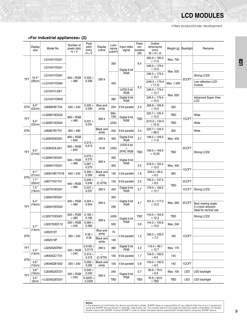
LCD
LCD MODULES
New product/Under development
<For industrial appliances> (2)
Display size Model No.
Number of pixels (dot)
H
×
V
Pixel pitch (mm) H
×
V
Display colors
Lumi-nance (cd/m
2
)
Input video signal
Power con-
sumption
(W)
Outline dimensions
(mm)W
×
H
×
D
Weight (g) Backlight Remarks
TFT 10.4
′′
(26cm)
LQ104V1DG21
640
×
RGB
×
4800.330
×
0.330 260 k
350
Digital 6 bit RGB
6.4
265.0
×
195.0
×
11.5 Max. 700
2CCFT
LQ104V1DG51 246.5
×
179.4
×
15.5Max. 620
LQ104V1DG61
4506.3
246.5
×
179.4
×
13.7 Strong LCD2
LQ104V1DG64 (246.5
×
179.4
×
17.2) Max. 1 000 Low reflection LCD module
LQ104V1LG61 LVDS 6 bit RGB
246.5
×
179.4
×
13.7Max. 620
LQ104V1DW02 380 Digital 6 bit RGB
246.5
×
179.4
×
15.5Advanced Super View LCD
STN 8.9
′′
(22cm) LM089HB1T04 640
×
240 0.330
×
0.330
Blue and white 250 8 bit parallel 2.3 258.8
×
109.8
×
10.0 320
1CCFTTFT8.5
′′
(22cm)
LQ085Y3DG03800
×
RGB
×
480 0.231
×
0.231
260 k
(Min. 130) Digital 6 bit
RGB TBD
222.7
×
135.4
×
12.5 TBD Wide
LQ085Y3DG04 (250) (212.0
×
134.0
×
12.5) TBD Wide
STN LM085YB1T01 800
×
480 Black and white 200 8 bit parallel 2.4 222.7
×
134.0
×
68.5 300 Wide
TFT 8.4
′′
(21cm)
LQ084S3DG01 800
×
RGB
×
6000.213
×
0.213
260 k 350 Digital 6 bit RGB 3.7 199.5
×
149.5
×
11.6 Max. 405
2CCFT
LQ084S3LG01 800
×
RGB
×
600 16 M (400)LVDS 6 bit
+2FRC RGB TBD 199.5
×
149.5
×
12.05 TBD Strong LCD2
LQ084V3DG01640
×
RGB
×
480
0.270
×
0.270
260 k400
Digital 6 bit RGB
LQ084V1DG21 0.267
×
0.270 300 5.5 216.0
×
152.4
×
12.0 Max. 4301CCFT
STN
8.1
′′
(21cm) LM081HB1T01B 640
×
240 0.300
×
0.300
Black and white 150 4 bit parallel 1.6 249.0
×
99.4
×
8.5 260
7.7
′′
(20cm) LM077VS1T01
640
×
RGB
×
480
0.246
×
0.246
–(C-STN) 150 8 bit parallel 2.5 195.2
×
137.5
×
8.0TBD
2CCFT
TFT
7.5
′′
(19cm)
LQ075V3DG01 0.237
×
0.237 260 k 400 Digital 6 bit
RGB 5.7 179.0
×
139.5
×
12.7 1CCFT Strong LCD2
6.4
′′
(16cm)
LQ064V3DG01640
×
RGB
×
4800.204
×
0.204 260 k
350Digital 6 bit
RGB 4.7 161.3
×
117.0
×
12.0 Max. 280 2CCFTLQ064V3DG04 290
Best viewing angle: 3 o’clock directionIdeal for vertical use
5.7
′′
(14cm)
LQ057V3DG01 640
×
RGB
×
4800.180
×
0.180
260 k(430)
Digital 6 bit RGB
TBD 144.0
×
104.6
×
12.3 TBD
1CCFT
Strong LCD2
LQ057Q3DC12 320
×
RGB
×
2400.360
×
0.360 500 3.9 144.0
×
104.6
×
13.0 Max. 240
STNLM32019T
320
×
240 0.36
×
0.36
Blue and white 70
4 bit parallel 1.2 166.0
×
109.0
×
7.5 160LM32019P Black and
white 100
TFT5.0
′′
(13cm)
LQ050Q5DR01320
×
RGB
×
240
0.3165
×
0.3115 260 k 380 Digital 6 bit
RGB 4.2 119.4
×
89.1
×
12.7 Max. 170
STNLM050QC1T01 0.315
×
0.315
–(C-STN) 100 8 bit parallel 1.7 134.0
×
100.0
×
8.5 145
4.6
′′
(12cm) LM046QB1S02 320
×
240 0.295
×
0.295
Black and white 100 4 bit parallel 0.9 134.0
×
100.0 × 8.5 140 1CCFT
TFT
3.8′′ (10cm) LQ038Q3DC01
320 × RGB × 240
0.240 × 0.240
260 k240
Digital 6 bit RGB
0.7 90.6 × 79.9 × 9.9 Max. 105 LED LED backlight
3.5′′ (9cm) LQ035Q3DG01 0.2205 ×
0.2205 TBD TBD 76.9 × 63.9 × TBD TBD LED LED backlight
NoticeIn the absence of confirmation by device specification sheets, SHARP takes no responsibility for any defects that may occur in equipment using any SHARP devices shown in catalogs, data books, etc. The models listed on this page are lead-free solder compatible. For details, please inquire with SHARP. Contact SHARP in order to obtain the latest device specification sheets before using any SHARP device.

TFT
10
LCD MODULES
New product
Under development
<For Information display>
*1 Pixel means a set of each RGB dot.*2 Excluding FPC for connection and other excessing parts.*3 LVDS: Low Voltage Differential Signaling(Note) Please note that the specifications are subject to change without prior notice for production improvement.
<For LCD TV>
*1 Pixel means a set of each RGB dot.*2 Excluding FPC for connection and other excessing parts.*3 LVDS: Low Voltage Differential Signaling(Note) Please note that the specifications are subject to change without prior notice for production improvement.
Display size (cm) [
′′
]
Model No.Number
of pixels*
1
Dot format H
×
V(dot)
Active areaH
×
V(mm)
Number of colors (color)
Outline dimensions*
2
W
×
H
×
D (TYP.)(mm)
Backlight Video interface
(Input video signal)
Remarks
TFT
163.8 [65]
LK645D3LZ2U
2 073 600
1 080
×
1 920
×
RGB803.52
×
1 428.48
16.77M
907.0
×
1 555.3
×
100.0
Built-in LVDS*
3
(8-bit digital)
PortraitAdvanced Super View LCDHigh luminance: 450cd/m
2
Wide viewing angle: L/R 176°/ U/D 176°High contrast: 2 000:1High-speed response [G to G]: 6ms (Ave.)
LK645D3LZ29 1 920
×
RGB
×
1 0801 428.48
×
803.52
1 555.3
×
907.0
×
100.0
Advanced Super View LCDHigh luminance: 450cd/m
2
Wide viewing angle: L/R 176°/ U/D 176°High contrast: 2 000:1High-speed response [G to G]: 6ms (Ave.)
132.1 [52] LK520D3LZ19 1 920
×
RGB
×
1 0801 152.0
×
648.0
1 219.0
×
706.7
×
69.8
Advanced Super View LCDHigh luminance: 450cd/m
2
Wide viewing angle: L/R 176°/ U/D 176°High contrast: 1 800:1High-speed response [G to G]: 6ms (Ave.)
116.8 [46] LK460D3LZ19 1 920
×
RGB
×
1 0801 018.0
×
573.0
1 083.0
×
627.0
×
65.7
Advanced Super View LCDHigh luminance: 450cd/m
2
Wide viewing angle: L/R 176°/ U/D 176°High contrast: 1 800:1High-speed response [G to G]: 6ms (Ave.)
Display size (cm) [
′′
]
Model No.Number
of pixels*
1
Dot format H
×
V(dot)
Active areaH
×
V(mm)
Number of colors (color)
Outline dimensions*
2
W
×
H
×
D (TYP.)(mm)
Backlight Video interface
(Input video signal)
Remarks
TFT
132.1 [52] LK520D3LZxx 2 073 600 1 920
×
RGB
×
1 0801 152
×
648
16.77M
(1 219
×
706.7
×
69.8)
Built-in LVDS*
3
(8-bit digital)
Advanced Super View LCDHigh luminance: 450cd/m
2
Wide viewing angle: L/R 176°/ U/D 176°High contrast: (1 500:1)120Hz drive compatible
116.8 [46] LK460D3LZxx 2 073 600 1 920
×
RGB
×
1 0801 018
×
573
(1 083
×
627
×
65.7)
Advanced Super View LCDHigh luminance: 500cd/m
2
Wide viewing angle: L/R 176°/ U/D 176°High contrast: (1 500:1)120Hz drive compatible
Notice
In the absence of confirmation by device specification sheets, SHARP takes no responsibility for any defects that may occur in equipment using any SHARP devices shown in catalogs, data books, etc. The models listed on this page are lead-free solder compatible. For details, please inquire with SHARP. Contact SHARP in order to obtain the latest device specification sheets before using any SHARP device.

11
LCD
LCD MODULES
New product
Under development
<For automotive applications> (1)
LQ065T9DZ03/LQ088H9DZ03: operating temperature (panel surface temperature) –40 to +85°C / storage temperature –40 to +95°C
LQ070Y5DG06/LQ080Y5DG03: operating temperature (panel surface temperature) –30 to 85°C / storage temperature –40 to 95°C
Other models: operating temperature (panel surface temperature) –30 to 85°C / storage temperature –40 to +85°C
*1 Number of pixels: 25 920 *2 Number of pixels: 28 160 *3 Number of pixels: 76 800*4 Number of pixels: 112 320 *5 Number of pixels: 93 600 *6 Number of pixels: 96 000*7 Number of pixels: 384 000 *8 Number of pixels: 115 200 *9 Number of pixels: 153 600*10 Excluding FPC for connection and other protruding parts.*11 MBK-PAL system is adopted as PAL. The LCD panel has 234 (240) scanning lines, and displays a picture of 273 (274) virtual scanning lines.*12 Video interface: External (Device specific external video interface IC is available.)(Note) Please refer to the latest relevant specificaiont sheets before using these devices.
Display size (cm) [
′′
]
Model No.Dot format
H
×
V(dot)
Pixel pitch H
×
V(mm)
Active areaH
×
V(mm)
Input signal
system
Input video signal
Back-light
Lumi-nance (cd/m
2
) (TYP.)
Power consump-tion (mW)
(TYP.)
Outline dimensions*
10
W
×
H
×
D (mm) (TYP.)
Weight (g)
(TYP.)Remarks
TFT
7.8 [3.1] LQ031B5DG01 270
×
RGB
×
96*
1
0.273
×
0.273
73.7
×
26.2
6-bit digital RGB
6-bit digital
Built-inLED 350 700 85.4
×
38.8
×
8.65 44
"Compact LCD" suitable for display in meter, Wide screen (8 : 3), LED back-light, 260K-color display, Wide viewing angle, RoHS compliant
8.3 [3.3] LQ033B5DG02 160
×
RGB
×
176*
2
0.351
×
0.349
56.2
×
61.4
6-bit digital RGB
6-bit digital
Built-in1CCFT 290 1 800 73
×
78.3
×
12.5 90
"Compact LCD" suitable for display in meter, High-speed response (low tem-perature), 260K-color dis-play, Wide viewing angle, RoHS compliant
8.9 [3.5]
LQ035Q5DG02 320
×
RGB
×
240*
3
0.222
×
0.222
71.0
×
53.3
6-bit digital RGB
6-bit digital
Built-inLED 500 TBD 86.4
×
84
×
6.7 TBD
"Compact LCD" suitable for display in meter, LED backlight, High lumi-nance, Thin, High-speed response (low tempera-ture), 260K-color display, Wide viewing angle, RoHS compliant
15 [6.1]
LQ061T5GG01 480
×
RGB
×
234*
4
0.284
×
0.308
136.1
×
72.0
NTSC/PAL*
11
TFT specific analog RGB*
12
Built-in1CCFT 500 3 200 149
×
82.9
×
7.2160
(Max.)
Wide QVGA (17:9), Thin, High luminance, Wide viewing angle, RoHS compliant
16 [6.5]
LQ065T5GG61 400
×
RGB
×
234*
5
0.359
×
0.339
143.4
×
79.3
NTSC/PAL*
11
TFT specific analog RGB*
12
Built-in1CCFT 400 3 300 155
×
89.2
×
8.8175
(Max.)
Wide QVGA (16:9), Thin, Wide viewing angle, RoHS compliant
LQ065T5DG02 400
×
RGB
×
240*
6
0.359
×
0.331
143.4
×
79.3
6-bit digital RGB
6-bit digital
Built-in1CCFT 620 4 100 155
×
89.2
×
9.1 170
Wide QVGA (16:9), Digital I/F, 260K-color display, High luminance, Wide viewing angle, RoHS compliant
LQ065T9DZ03 400
×
RGB
×
240*
6
0.359
×
0.331
143.4
×
79.3
6-bit digital RGB
6-bit digital
Built-in1CCFT 250 5 200 155
×
89.2
×
12.5205
(Max.)
"Super Mobile LCD" with high visibility under bright ambient light, Wide QVGA (16:9), Wide viewing angle, Gray-scale inver-sion free, 260K-color dis-play, RoHS compliant
Notice
In the absence of confirmation by device specification sheets, SHARP takes no responsibility for any defects that may occur in equipment using any SHARP devices shown in catalogs, data books, etc. The models listed on this page are lead-free solder compatible. For details, please inquire with SHARP. Contact SHARP in order to obtain the latest device specification sheets before using any SHARP device.

TFT
12
LCD MODULES
New product
Under development
<For automotive applications> (2)
LQ065T9DZ03/LQ088H9DZ03: operating temperature (panel surface temperature) –40 to +85°C / storage temperature –40 to +95°C
LQ070Y5DG06/LQ080Y5DG03: operating temperature (panel surface temperature) –30 to 85°C / storage temperature –40 to 95°C
Other models: operating temperature (panel surface temperature) –30 to 85°C / storage temperature –40 to +85°C
*1 Number of pixels: 25 920 *2 Number of pixels: 28 160 *3 Number of pixels: 76 800*4 Number of pixels: 112 320 *5 Number of pixels: 93 600 *6 Number of pixels: 96 000*7 Number of pixels: 384 000 *8 Number of pixels: 115 200 *9 Number of pixels: 153 600*10 Excluding FPC for connection and other protruding parts.*11 MBK-PAL system is adopted as PAL. The LCD panel has 234 (240) scanning lines, and displays a picture of 273 (274) virtual scanning lines.*12 Video interface: External (Device specific external video interface IC is available.)(Note) Please refer to the latest relevant specificaiont sheets before using these devices.The Tenri site NF3 (JQA-AU0121-1) and plants No. 1 and No. 2 (JQA-AU0121-2) at the Mie site of the Mobile Liquid Crystal Display Group have been certified under the ISO/TS 16949:2002 Quality Management System. [Certifying organization: Japan Quality Assurance Organization (JQA)]
Display size (cm) [
′′
]
Model No.Dot format
H
×
V(dot)
Pixel pitch H
×
V(mm)
Active areaH
×
V(mm)
Input signal
system
Input video signal
Back-light
Lumi-nance (cd/m
2
) (TYP.)
Power consump-tion (mW)
(TYP.)
Outline dimensions*
10
W
×
H
×
D (mm) (TYP.)
Weight (g)
(TYP.)Remarks
TFT
18 [7]
LQ070T5GG21 480
×
RGB
×
234*
4
0.326
×
0.352
156.2
×
82.4
NTSC/PAL*
11
TFT specific analog RGB*
12
Built-in1CCFT 500 3 500 167
×
93
×
6.9195
(Max.)
Wide QVGA (17:9), Thin, High luminance, Wide viewing angle, RoHS compliant
LQ070T5DR05 480
×
RGB
×
240*
8
0.321
×
0.363
154.1
×
87.0
6-bit digital RGB
6-bit digital
Built-in2CCFT 400 5 100 170.1
×
103.4
×
14.2280
(Max)
Wide QVGA (16:9), Digital I/F, 260K-color display, Wide viewing angle
LQ070Y5DG05 800
×
RGB
×
480*
7
0.195
×
0.1725
156.0
×
82.8
6-bit digital RGB
6-bit digital
Built-in1CCFT 460 3 600 167
×
93
×
7.2196
(Max.)
High resolution (wide VGA/17:9), Thin, W-QVGA (GG21) vertical/horizontal compatible, 260K-color display, Wide viewing angle, RoHS compliant
LQ070Y5DG06 800
×
RGB
×
480*
7
0.191
×
0.191
152.4
×
91.4
6-bit digital RGB
6-bit digital
Built-inLED 430* TBD 170
×
104
×
8.0 TBD
High resolution (wide VGA/15:9), High color purity (65% of NTSC), High-speed response (low temperature), LED back-light, Thin, 260K-color dis-play, Wide viewing angle, RoHS compliant, * Luminosity at eye point
LQ070Y5DE02 800
×
RGB
×
480*
7
0.195
×
0.1725
156.0
×
82.8
6-bit digital RGB
6-bit digital
Built-inLED 320* 5 250 167.5
×
93.2
×
6.5 to 9.0215
(Max.)
Dual directional viewing LCD, Wide screen (17:9), LED backlight, Thin, 260K-color display, Wide viewing angle, RoHS compliant,
* DV luminosity at eye point
20 [8]
LQ080Y5DG03 800
×
RGB
×
480*
7
0.2175
×
0.2175
174.0
×
104.4
6-bit digital RGB
6-bit digital
Built-inLED 430* TBD 190
×
120
×
8.0 TBD
High resolution (wide VGA/15:9), High color purity (65% of NTSC), High-speed response (low temperature), LED back-light, Thin, 260K-color dis-play, Wide viewing angle, RoHS compliant, * Luminosity at eye point
LQ080Y5DG04 800
×
RGB
×
480*
7
0.2175
×
0.2175
174.0
×
104.4
6-bit digital RGB
6-bit digital
Built-in2CCFT 625 5 900 190
×
120
×
13 392
High resolution (wide VGA/15:9), High-speed response (low tempera-ture), High luminosity, 260K-color display, Wide viewing angle
LQ080Y5CGXX 800
×
RGB
×
480*
7
0.222
×
0.207
177.6
×
99.4
NTSC/PAL/PAL (60)
Composite
Built-in1CCFT 400 10 400 198
×
117
×
17.9 391
High resolution (wide VGA/16:9), All-in-one, Wide viewing angle, RoHS compliant
22 [8.8]
LQ088H9DZ03 640
×
RGB
×
240*
9
0.327
×
0.327
209.3
×
78.5
6-bit digital RGB
6-bit digital
Built-in2CCFT 250 7 100 231.6
×
103.25
×
14.4370
(Max.)
"Super Mobile LCD" with high visibility under bright ambient light, Wide screen (8:3), Wide viewing angle, Gray-scale inversion free, 260K-color display, RoHS compliant
Notice
In the absence of confirmation by device specification sheets, SHARP takes no responsibility for any defects that may occur in equipment using any SHARP devices shown in catalogs, data books, etc. The models listed on this page are lead-free solder compatible. For details, please inquire with SHARP. Contact SHARP in order to obtain the latest device specification sheets before using any SHARP device.

13
LCD
LCD MODULES
New product
Under development
<For personal AV>
*1 Number of Pixels: 230 400*2 Number of Pixels: 115 200*3 MBK-PAL system is adopted as PAL. The LCD panel has 234 (220) scanning lines, and displays a picture of 273 (256) virtual scanning lines.*4 Video interface: Internal*5 Excluding FPC for connection and other excessing parts.* CG Silicon ... Continuous grain silicon technology developed jointly with Semiconductor Energy Laboratory Co. Ltd. is used.(Note) Please refer to the latest relevant specification sheets before using these devices.
<For mobile phones>
*1 Number of Pixels: 76 800*2 Number of Pixels: 20 480*3 Number of Pixels: 16 384*4 Excluding FPC for connection and other excessing parts.* CG Silicon ... Continuous grain silicon technology developed jointly with Semiconductor Energy Laboratory Co. Ltd. is used.(Note) Please refer to the latest relevant specification sheets before using these devices.
Display size (cm) [
′′
]
Model No.
Dot format H
×
V(dot)
Pixel pitch H
×
V(mm)
Active areaH
×
V(mm)
Input signal
system
Input video signal
Back-light
Lumi-nance (cd/m
2
) (TYP.)
Power consump-tion (mW)
(TYP.)
Outline dimensions*
5
W
×
H
×
D (mm) (TYP.)
Weight (g)
(TYP.)Remarks
CG Silicon
6.4 [2.5]
LS025A8DZ01
960
×
240*
1
0.052
×
0.156
(Dot pitch)
49.9
×
37.4
NTSC/PAL*
3
8-bit digital RGB
Built-in LED
250 230 56.2
×
47.8
×
2.7 21
Super Mobile LCD with high outdoor visibility due to transflectivity, Top/bottom and left/right angle of view 160°, Delta configuration, High contrast, Low power consumption
6.8 [2.7] LS027T3DG01 0.062
×
0.139
59.49
×
33.48 250 220 65
×
45
×
2.5 13
TFT 6.4 [2.5]
LQ025A3DS01480
×
RGB
×
240*
2
0.104
×
0.156
49.87
×
37.44 250 180 60.0
×
44.3
×
2.7 14
RGB delta configuration, FPC side positioning, RoHS compliant, Lead-free solder compatible
Display size (cm) [
′′
]
Model No.Dot format
H
×
V(dot)
Pixel pitch H
×
V(mm)
Active areaH
×
V(mm)
Input video signal
Back-light
Contrast ratio (Transmissive/
Reflective)
Luminance (cd/m
2
) (TYP.)
Outline dimensions*
4
W
×
H
×
D (mm) (TYP.)
Weight (g)
(TYP.)Remarks
CG Silicon
5.6 [2.2]
LS022Q8UX05 240
×
RGB
×
320*
1
0.1395
×
0.1395
33.48
×
44.64
16-bit parallelCPU Built-in
LED
400 : 1 (Transmissive)/
10 : 1 (Reflective)
300 39.2
×
58.35
×
2.3 T.B.D.
Super Mobile LCD with high outdoor visibility due to transflectivity, Top/bottom and left/right angle of view 160° (CR
7
5), High contrast, 260k-color display, RoHS compliant
7.0 [2.75] LS028B7UX01 240
×
RGB
×
4000.05
×
0.15
36.0
×
60.0 CPU bus 400 : 1 250 41.8
×
70.5
×
2.3 10Transmissive type, 260k-color display, RoHS compliant
Notice
In the absence of confirmation by device specification sheets, SHARP takes no responsibility for any defects that may occur in equipment using any SHARP devices shown in catalogs, data books, etc. The models listed on this page are lead-free solder compatible. For details, please inquire with SHARP. Contact SHARP in order to obtain the latest device specification sheets before using any SHARP device.

EL
14
EL DISPLAY MODULES
EL Display Modules
*1 In case of frame frequency = 120 Hz*2 Excluding FPC for connection and other excessing parts.(Note) Please refer to the latest relevant specification sheets before using these devices.
Display size
(cm) [
′′
]Model No.
Dot format H
×
V(dot)
Dot pitch H
×
V(mm)
Active area H
×
V(mm)
Areal luminance
(cd/m
2
) (TYP.)
Supply voltage
(V)
Power consumption
(W) (TYP.)
Operating temperature
(°C)
Outline dimensions*
2
W
×
H
×
D (mm) (TYP.)
Weight (g)
(TYP.)Remarks
23 [8.9]LJ64H034
640
×
400 0.30
×
0.30 191.9
×
119.9
110*
1
+5, +12 11 –5 to +55
246.0
×
175.0
×
19.0 450 High luminance, Wide viewing angle
LJ089MB2S01 60 246.0
×
158.0
×
26.0 390 Wide viewing angle
LJ089MB2S01
Notice
In the absence of confirmation by device specification sheets, SHARP takes no responsibility for any defects that may occur in equipment using any SHARP devices shown in catalogs, data books, etc. The models listed on this page are lead-free solder compatible. For details, please inquire with SHARP. Contact SHARP in order to obtain the latest device specification sheets before using any SHARP device.
!
LSI
15
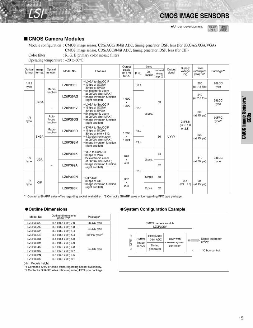
CMOS IMAGE SENSORS
Under development
CMOS Camera Modules
Module configuration : CMOS image sensor, CDS/AGC/10-bit ADC, timing generator, DSP, lens (for UXGA/SXGA/VGA) CMOS image sensor, CDS/AGC/8-bit ADC, timing generator, DSP, lens (for CIF)
Color filter : R, G, B primary color mosaic filtersOperating temperature : –20 to 60°C
Outline Dimensions
System Configuration Example
UXGA
SXGA
VGA
CIF
–
–
FeaturesModel No.
Outputpixels(H x V)MAX.
Lens
F No.Con-
figuration
Horizontalviewingangle (°)
Outputsignal
Supplyvoltage
(V)
Powerconsumption(mW) TYP.
Package*1Opticalfunction
Imageformat
Opticalformat
*1 Contact a SHARP sales office regarding socket availability. *2 Contact a SHARP sales office regarding FPC type package.
24LCCtype
30FPCtype*2
28LCCtype
24LCCtype
• UXGA to SubQCIF• 10 fps at UXGA/
30 fps at SVGA• 5x electronic zoom
at QVGA size (MAX.)• Image inversion function
(right and left)
• UXGA to SubQCIF• 15 fps at UXGA/
30 fps at SVGA• 5x electronic zoom
at QVGA size (MAX.)• Image inversion function
(right and left)
• VGA to SubQCIF• 30 fps at VGA• 2x electronic zoom
at QVGA size (MAX.)• Image inversion function
(right and left)
• CIF/QCIF• 30 fps at CIF• Image inversion function
(right and left)
• SXGA to SubQCIF• 15 fps at SXGA/
30 fps at 640 x 512• 4.2x electronic zoom
at QVGA size (MAX.)• Image inversion function
(right and left)
1/3.2type
1/6type
1/7type
1/4type
Macrofunction
Macrofunction
2.5(I/O : 2.8)
UYVY
640x
480
352x
288
F3.4
F2.8
F3.2
F3.4
F2.8
53
56
54
52
58
52
2.8/1.8(I/O : 1.8or 2.8)
3 pcs.
2 pcs.
Single
2 pcs.
290(at 7.5 fps)
240(at 7.5 fps)
200(at 15 fps)
220(at 15 fps)
110(at 30 fps)
35(at 15 fps)
1 600x
1 200
1 280x
1 024
LZ0P3955
LZ0P39AG
LZ0P395V
LZ0P39DS
LZ0P393D
LZ0P393M
LZ0P394K
LZ0P399A
LZ0P392N
LZ0P396K
Autofocus
function
LZ0P3955LZ0P39AGLZ0P395VLZ0P39DSLZ0P393DLZ0P393MLZ0P394KLZ0P399ALZ0P392NLZ0P396K
9.5 x 9.5 x (H) 7.08.0 x 8.0 x (H) 4.88.0 x 8.0 x (H) 4.48.5 x 8.5 x (H) 5.48.4 x 8.4 x (H) 5.38.0 x 8.0 x (H) 4.96.5 x 6.2 x (H) 4.35.8 x 5.8 x (H) 3.76.5 x 6.5 x (H) 4.56.0 x 6.0 x (H) 3.1
Model No. Outline dimensions(mm) TYP. Package*1
24LCC type
30FPC type*2
28LCC type
24LCC type
(H) : Module height *1 Contact a SHARP sales office regarding socket availability. *2 Contact a SHARP sales office regarding FPC type package.
CMOS camera moduleLZ0P395V
DSP withcamera system
controller
CMOSimagesensor Timing
generator
CDS/AGC/10-bit ADC
Le
ns
I2C bus control
Digital output forUYVY
CMOS
Imag
e Se
nsor
s/CC
Ds
"

LSI
16
CCDs
Higher-resolution CCDs
1/3-type CCDs
12 520 k
8 500 k
5 190 k
6 360 k
7 400 k
8 500 k
10 540 kRJ21W3BB0ET
RJ21W3BC0ET
RJ21Y3BA0ET
RJ21V3BC0ET
RJ23S3BD0ET
RJ23S3CD0ET
RJ23S3BE0BT
RJ23S3CE0BT
RJ23T3BB0ET
RJ23T3CB0ET
RJ23T3BC0BT
RJ23T3CC0BT
RJ23U3BA0ET
RJ23U3CA0ET
RJ23U3BC0BT
RJ23U3CC0BT
RJ23V3BA0BT
RJ23V3CA0BT
–
–
–
–
–
–
–
3 704 x 2 784
4 040 x 3 032
3 320 x 2 496
2 600 x 1 944
2 872 x 2 160
3 096 x 2 328
3 320 x 2 496
2.05 x 2.05
1.88 x 1.88
2.2 x 2.2
2.05 x 2.05
1.9 x 1.9
1.75 x 1.75
100
105
130
100
95
105
100
–88
–83
–88
–85
P-SOP032-0525
P-SOP028-0400
1/1.7type
1/1.8type
1/2.5type
Totalpixels
Opticalformat Color filter
R,G,Bprimary colormosaic filters
Model No. PackagePixel size
H x V (µm2)30 fps VGA
movieSensitivity(mV) TYP.
Smear ratio(dB) TYP.Image pixels (H x V)
Resolution
(25 fps VGA movie)
(22 fps VGA movie)
270 k
320 k
410 k
470 k
NTSC
PAL
NTSC
PAL
RJ2311AA0PB
RJ2311BA0PB
RJ2321AA0PB
RJ2321BA0PB
RJ2351AA0BB
RJ2351BA0AB
RJ2361AA0BB
RJ2361BA0AB
330
480
512 x 492
512 x 582
768 x 494
752 x 582
9.6 x 7.5
9.6 x 6.3
9.6 x 6.34
6.4 x 7.5
6.5 x 6.3
6.53 x 6.39
1 300
2 000
1 300
2 000
800
1 500
750
1 500
–120
–130
–120
–130
–105
–120
–105
–120
P-DIP016-0500C
N-DIP016-0450
Color
Totalpixels Standard Model No. Package
Pixel sizeH x V (µm2)
Sensitivity(mV) TYP.
Smear ratio(dB) TYP.Image pixels (H x V)Horizontal TV lines
Resolution
#

17
CCDs
Under development
1/3.8-type CCD
1/4-type CCDs
1/3-type CCDs with Dual-power-supply (5 V/12 V) Operation*
1
290 k NTSC RJ2311AA0PB* 330 532 x 512 7.2 x 5.6 1 200 –120 P-DIP014-0400AColor
Totalpixels Standard Model No. Package
Pixel sizeH x V (µm2)
Sensitivity(mV) TYP.
Smear ratio(dB) TYP.Image pixels (H x V)Horizontal TV lines
Resolution
* Suitable for intense light exposure.
270 k
320 k
410 k
470 k
NTSC
PAL
NTSC
PAL
RJ2411AA0PB*
RJ2411AB0PB
RJ2411BA0PB*
RJ2411BB0PB
RJ2421AB0PB
RJ2421BB0PB
RJ2451AA0PB
RJ2451BA0PB
RJ2461AA0PB
RJ2461BA0PB
330
480
512 x 492
512 x 582
768 x 494
752 x 582
7.2 x 5.6
7.2 x 4.7
7.2 x 4.73
4.9 x 5.6
5.0 x 4.7
5.0 x 4.77
800
1 200
720
1 100
400
600
400
600
–105
–120
–105
–120
–90
–114
–90
–114
P-DIP014-0400AColor
Totalpixels Standard Model No. Package
Pixel sizeH x V (µm2)
Sensitivity(mV) TYP.
Smear ratio(dB) TYP.
* Suitable for intense light exposure.
Image pixels (H x V)Horizontal TV lines
Resolution
270 k
320 k
EIA
CCIR
LZ2316A3
LZ2326A3380
512 x 492
512 x 582
9.6 x 7.5
9.6 x 6.3
3 300*2
3 000*2–110 N-DIP016-0500CB/W
Totalpixels Standard Model No. Package
Pixel sizeH x V (µm2)
Sensitivity(mV) TYP.
Smear ratio(dB) TYP.
*1 With mirror image function *2 When IR cut-off filter is not used.
Image pixels (H x V)Horizontal TV lines
Resolution
CMOS
Imag
e Se
nsor
s/CC
Ds

LSI
18
CCDs
Under development
CCD Peripheral ICs/LSIs
P-QFP048-0707/P-VQFN052-0707
P-VQFN064-0808/TFBGA068-0606
P-QFP048-0707
P-SSOP024-0275
P-VQFN036-0505
P-QFP048-0707
P-QFP048-0707
P-VQFN036-0606
P-VQFN032-0505
LFBGA192-1010
LFBGA140-0909
LFBGA168-1212/LFBGA171-0811
LFBGA171-0811
LR385851
LR386431/33
LR38653
LR38677
LR36B11
LR38678
LR38675
LR38667
IR3Y50U6
IR3Y60U6
IR3Y48A3/A5
IR3Y48B1
LR36689U
LR36687U/Y
LR366851
IR3Y30M2
Description Model No. Features Package
Electronic shutter, electronic exposure, mirror image function,for B/W CCDs, level shifter, smooth shutter, line lock function
For 270-k/320-kpixel CCDswith dual-power-supplyoperation (5 V/12 V)
<Timing generator> Monitoring mode/still mode<V driver> Vertical pulse driver for CCDs, 2-level output x 10, 3-level output x 10, 2-level output circuit for electronic shutter<CDS/PGA/ADC> 30 MHz (LR38667)/ 36 MHz (LR38675/LR38678/LR38677), high-speed S/H circuit, high-gain PGA circuit, 12-bit ADC, 12-bit digital output
<V driver> Vertical pulse driver for CCDs, 2-level output x 2, 3-level output x 2, 2-level output circuit for electronic shutter<CDS/PGA/ADC> 18 MHz, high-speed S/H circuit, high-gain PGA circuit, 10-bit ADC<DSP> 9-bit DAC, synchronous signal generation circuit, CCD drive timing generator, AE control function, AWB control function, mirror image function, YUV digital output, NTSC/PAL analog output
<V driver> Vertical pulse driver for CCDs, 2-level output x 2, 3-level output x 2, 2-level output circuit for electronic shutter<CDS/PGA/ADC> 25 MHz, high-speed S/H circuit, high-gain PGA circuit, 12-bit ADC<DSP> 10-bit DAC, synchronous signal generation circuit, CCD drive timing generator, AE control function, AWB control function, lens shading correction function, auto white blemish compensation function, mirror image function, YUV digital output, NTSC/PAL analog output
For 1/2.5-type 7 400-kpixel CCDs with/without movie function
For 1/2.5-type 5 190-kpixel,6 360-kpixel, 7 400-kpixel,8 500-kpixel CCDs with/withoutmovie function,For 1/1.8-type 8 500-kpixel,1/1.7-type 10 540-kpixel,12 520-kpixel CCDs with moviefunction
For 1/1.8-type 8 500-kpixel,1/1.7-type 10 540-kpixel CCDswith movie function
For 270-k/320-k/410-k/470-kpixel CCDs
Single-chip driverTiming generator
+Synchronous signal generator( )
Timing generator+
V driver+
CDS/PGA/ADC
V driver
CDS/PGA/ADC
Signal processor
V driver+
CDS/PGA/ADC+
DSP
For 1/2.5-type 5 190-kpixel CCDs with/without movie function
For 1/2.5-type 6 360-kpixel CCDswith/without movie function
Low power consumption [75 mW (TYP.) ],high-speed S/H circuit, high-gain PGA circuit, 12-bit ADC (25 MHz), 12-bit digital output
Low power consumption [69 mW (TYP.) ],high-speed S/H circuit, high-gain PGA circuit, 10-bit ADC (20 MHz), 10-bit digital output
Low power consumption [80 mW (TYP.) ],high-speed S/H circuit, high-gain PGA circuit, 10-bit ADC (18 MHz), 10-bit digital output
Low power consumption [80 mW (TYP.) ],high-speed S/H circuit, high-gain PGA circuit, 10-bit ADC (18 MHz), 10-bit digital output
Vertical pulse driver for CCDs, 2-level output x 4, 3-level output x 8,2-level output circuit for electronic shutter
Vertical pulse driver for CCDs, 2-level output x 10, 3-level output x 10,2-level output circuit for electronic shutter
Vertical pulse driver for CCDs, 2-level output x 2, 3-level output x 4,2-level output circuit for electronic shutter
Available for signal processing from CCD output to 75 Ω video output, for B/W CCDs, comparator for electronic exposure, high-speed S/H circuit, H aperture, LPF, AGC
<Timing generator> Programmable timing generator<V driver> Vertical pulse driver for CCDs, 2-level output x10, 3-level output x10 2-level output circuit for electronic shutter<CDS/PGA/ADC> 40 MHz, high-speed S/H circuit, high-gain PGA circuit, 22-bit ADC, 16-bit digital output

19
CCDs
Under development
CCD Peripheral ICs/LSIs (cont’d)
P-LQFP080-1212
P-TQFP128-1414
B-VQFN8(1.50 mm x 1.50 mm)
P-VQFN032-0505
LR386032
LR38627
IR3T47G
P-LQFP100-1414LR386071
IR3M55U*2
IR3M59U
IR3M61U*2
IR3M63U
DSP
LFBGA171-0811LR38654
V driver+
CDS/PGA/ADC+
DSP
Description Model No. Features Package
*1 Only support for 290-kpixel CCD.*2 For in-vehicle use
For 270-k/320-k/410-k/470-kpixel CCDs
9-bit DAC, synchronous signal generation circuit, built-in CCD drive timing generator, AE control function, AWB control function, mirror image function, YUV digital output, NTSC/PAL analog output
For 270-k/290-k/320-k/410-k/470-kpixel CCDs
<V driver> Vertical pulse driver for CCDs, 2-level output x 2, 3-level output x 2, 2-level output circuit for electronic shutter<CDS/PGA/ADC> 25 MHz, high-speed S/H circuit, high-gain PGA circuit, 12-bit ADC<DSP> 10-bit DAC, synchronous signal generation circuit, built-in CCD drive timing generator, AE control function, AWB control function, lens shading correction function, auto white blemish compensation function, mirror image function, electronic optical axis adjustment function*1, YUV digital output, NTSC/PAL analog output
10-bit DAC, synchronous signal generation circuit, built-in CCD drive timing generator, AE control function, AWB control function, lens shading correction function, auto white blemish compensation function, mirror image function, YUV digital output, NTSC/PAL analog output
Input voltage range : 11.5 to 16 V,Constant current range : 1 to 5.5 mA,ON/OFF control for constant current
9-bit DAC, synchronous signal generation circuit, built-in CCD drive timing generator, AE control function, AWB control function, mirror image function, YUV digital output, NTSC/PAL analog output, Y/C separation analog output, line lock function
Power supply IC forCCDs and peripheral
ICs/LSIs
Buffer ICfor CCD output
circuit
For 270-k/320-kpixel CCDs
For 270-k/290-k/320-k/410-k/470-kpixel CCDs
For 5 190-kpixel to 12 520-kpixel CCDs
Input voltage range : 4.5 to 16 V,PWM control + charge pump system,output voltage : three outputs (15 V/12 V, –8 V/–5 V, 3.3 V),power sequencing circuit, overcurrent protection circuit
Input voltage range : 4.5 to 10 V,PWM control + charge pump system,output voltage : four outputs (15 V, –8 V, 3.3 V, 1.8 V),power sequencing circuit, overcurrent protection circuit
CMOS
Imag
e Se
nsor
s/CC
Ds

LSI
20
CCDs
Under development
System Configuration Examples
• High-resolution Digital Camera System with Three-chip Configuration
Four-power-supply CCDs and peripheral IC/LSIs
Timing generator+
V driver+
CDS/PGA/ADC
Four-power-supplyCCD
*Refers to the following table regarding adaptable CCDs with IR3T47G.
Buffer IC forCCD output circuit
Analog output for RGB/NTSC/PAL
Digital LCD interface
Interface
InterfaceCompactFlashTM
orSmartMediaTM
orSD memory card
LCD panel
Flashmemory
SDRAM
IR3T47G*
USB
Image processing LSIfor digital cameras
Timing generator + V driver+ CDS/PGA/ADC
30 fps VGAmovie
CCDBuffer IC for
CCD output circuit
1/1.7 type
1/1.8 type
1/2.5 type
(25 fps VGA movie)
(22 fps VGA movie)
RJ21W3BB0ET
RJ21W3BC0ET
RJ21Y3BA0ET
RJ21V3BC0ET
RJ23S3BD0ET
RJ23S3CD0ET
RJ23S3BE0BT
RJ23S3CE0BT
RJ23T3BB0ET
RJ23T3CB0ET
RJ23T3BC0BT
RJ23T3CC0BT
RJ23U3BA0ET
RJ23U3CA0ET
RJ23U3BC0BT
RJ23U3CC0BT
RJ23V3BA0BT
RJ23V3CA0BT
IR3T47G
IR3T47G
IR3T47G
IR3T47G
10 540 k pixels
12 520 k pixels
8 500 k pixels
5 190 k pixels
6 360 k pixels
7 400 k pixels
8 500 k pixels
–
–
–
–
–
–
–
–
–
–
LR38677/LR36B11
LR36B11
LR38677/LR36B11
LR38667/LR36B11
LR38675/LR36B11
LR38678/LR36B11
LR36B11
–
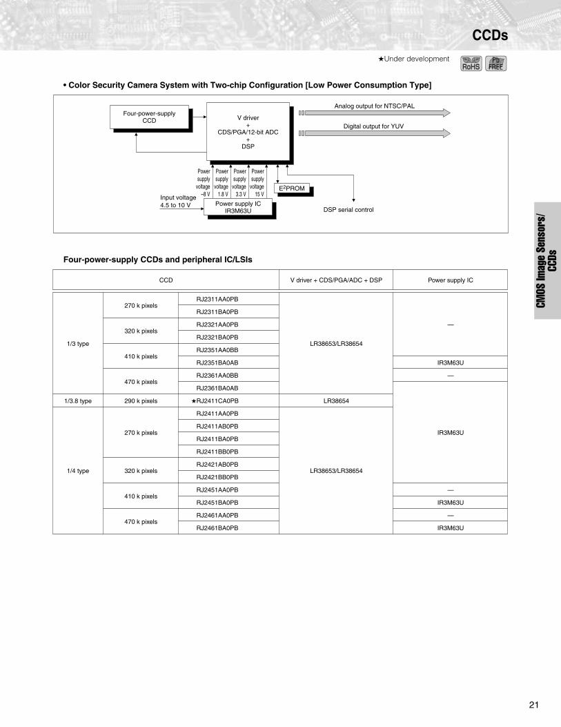
21
CCDs
Under development
• Color Security Camera System with Two-chip Configuration [Low Power Consumption Type]
Four-power-supply CCDs and peripheral IC/LSIs
V driver+
CDS/PGA/12-bit ADC+
DSP
DSP serial control
Four-power-supplyCCD
Powersupply
voltage–8 V
Powersupply
voltage1.8 V
Powersupply
voltage3.3 V
Powersupply
voltage15 V
Analog output for NTSC/PAL
Digital output for YUV
Power supply ICIR3M63U
Input voltage4.5 to 10 V
E2PROM
V driver + CDS/PGA/ADC + DSP
270 k pixels
320 k pixels
410 k pixels
470 k pixels
290 k pixels
270 k pixels
320 k pixels
410 k pixels
470 k pixels
1/3 type
1/3.8 type
1/4 type
Power supply IC
RJ2311AA0PB
RJ2311BA0PB
RJ2321AA0PB
RJ2321BA0PB
RJ2351AA0BB
RJ2351BA0AB
RJ2361AA0BB
RJ2361BA0AB
RJ2411CA0PB
RJ2411AA0PB
RJ2411AB0PB
RJ2411BA0PB
RJ2411BB0PB
RJ2421AB0PB
RJ2421BB0PB
RJ2451AA0PB
RJ2451BA0PB
RJ2461AA0PB
RJ2461BA0PB
—
IR3M63U
—
IR3M63U
—
IR3M63U
—
IR3M63U
LR38653/LR38654
LR38654
LR38653/LR38654
CCD
CMOS
Imag
e Se
nsor
s/CC
Ds
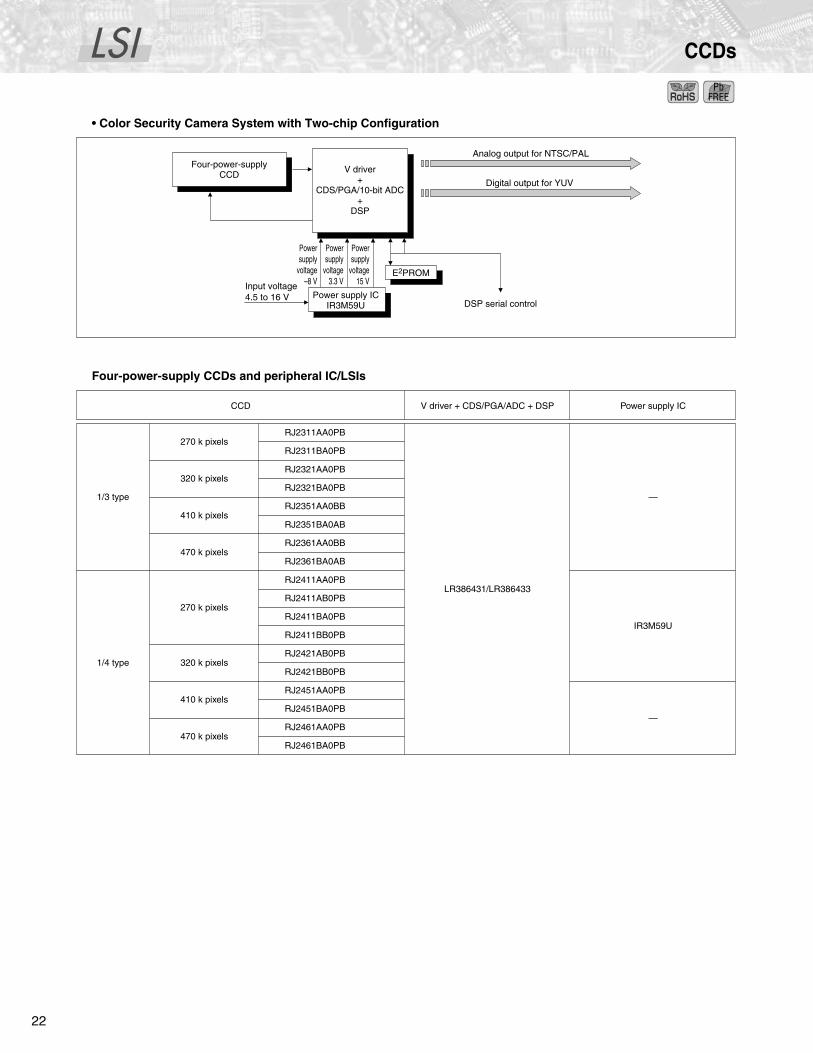
LSI
22
CCDs
• Color Security Camera System with Two-chip Configuration
Four-power-supply CCDs and peripheral IC/LSIs
V driver+
CDS/PGA/10-bit ADC+
DSP
DSP serial control
Four-power-supplyCCD
Powersupply
voltage–8 V
Powersupply
voltage3.3 V
Powersupply
voltage15 V
Analog output for NTSC/PAL
Digital output for YUV
Power supply ICIR3M59U
Input voltage4.5 to 16 V
E2PROM
V driver + CDS/PGA/ADC + DSP
270 k pixels
320 k pixels
410 k pixels
470 k pixels
270 k pixels
320 k pixels
410 k pixels
470 k pixels
1/3 type
1/4 type
Power supply IC
RJ2311AA0PB
RJ2311BA0PB
RJ2321AA0PB
RJ2321BA0PB
RJ2351AA0BB
RJ2351BA0AB
RJ2361AA0BB
RJ2361BA0AB
RJ2411AA0PB
RJ2411AB0PB
RJ2411BA0PB
RJ2411BB0PB
RJ2421AB0PB
RJ2421BB0PB
RJ2451AA0PB
RJ2451BA0PB
RJ2461AA0PB
RJ2461BA0PB
CCD
LR386431/LR386433
—
IR3M59U
—

23
CCDs
Under development
• Color Security Camera System with Four-chip Configuration
Four-power-supply CCDs and peripheral ICs/LSIs (1)
CDS/PGA/ADCAnalog output for NTSC/PAL
Digital output for YUV
V driverLR366851
Four-power-supplyCCD
DSP serial controlPower supply IC
DSP
E2PROM
V driver CDS/PGA/ADC
270 k pixels
320 k pixels
410 k pixels
470 k pixels
270 k pixels
320 k pixels
410 k pixels
470 k pixels
1/3 type
1/4 type
Power supply ICCCD
RJ2311AA0PB
RJ2311BA0PB
RJ2321AA0PB
RJ2321BA0PB
RJ2351AA0BB
RJ2351BA0AB
RJ2361AA0BB
RJ2361BA0AB
RJ2411AB0PB
RJ2411BB0PB
RJ2421AB0PB
RJ2421BB0PB
RJ2451AA0PB
RJ2451BA0PB
RJ2461AA0PB
RJ2461BA0PB
LR366851IR3Y60U6IR3Y48A3/A5/B1
IR3Y48A3/A5/B1
LR386071,LR386032,LR386071
+++
—
IR3M59U
—
DSP
CMOS
Imag
e Se
nsor
s/CC
Ds

LSI
24
CCDs
Four-power-supply CCDs and peripheral ICs/LSIs (2)
• B/W Security Camera System
Dual-power-supply CCDs and peripheral IC/LSI for analog interface
V driver
270 k pixels
320 k pixels
410 k pixels
470 k pixels
270 k pixels
320 k pixels
410 k pixels
470 k pixels
1/3 type
1/4 type
Power supply ICCCD CDS/PGA/ADC
RJ2311AA0PB
RJ2311BA0PB
RJ2321AA0PB
RJ2321BA0PB
RJ2351AA0BB
RJ2351BA0AB
RJ2361AA0BB
RJ2361BA0AB
RJ2411AB0PB
RJ2411BB0PB
RJ2421AB0PB
RJ2421BB0PB
RJ2451AA0PB
RJ2451BA0PB
RJ2461AA0PB
RJ2461BA0PB
LR366851 IR3Y50U6
DSP
LR38627
—
IR3M63U
—
IR3M63U
—
IR3M63U
—
IR3M63U
Dual-power-supplyCCD
Analog signal processorIR3Y30M2
Single-chip driver with level shifterLR385851
Power supplyvoltage 12 V
Power supplyvoltage 5 V
Analog output for EIA/CCIR
Single-chip driver(Timing generator + Synchronous signal generator) Signal processor
270 k pixels
320 k pixels1/3 type
CCD
LR385851 IR3Y30M2LZ2316A3
LZ2326A3
!

25
LSIs FOR LCDs
For Notebook PCs, PC Monitors and LCD TVs
TFT-LCD Drivers
TCP/SOF
SOF
SOF
TCP/SOF/COG
85
0.1
0.2
13.5
15
16.5
16
15
33
384
480
384
64 levels
256 levels
-
200/240/256/263/
270
384/402/408/414/
420
240
256 42
45
480/504/516/528
630/642
684/690/702/720
402/414420/432
384/414/420
LH16AM
LH16B6
LH16AD
LH16B5
LH16B9
LH16AE
LH16BP
LH16AW
LH16AF
LH1691
LH1694
LH169J
Drive function
Dotinversion
drive
Gate driver
Model No. Grayscale
No. ofLCD drive
outputs
Clockfrequency
(MHz) MAX.PackageDescription
Displayvoltage
(V) MAX.
Supplyvoltage
(V)
Sourcedriver
2.7 to 3.6
2.3 to 3.6
2.7 to 3.6
2.3 to 3.6
2.7 to 3.6
3.0 to 5.5
2.7 to 3.6
2.4 to 4.2
Low EMI*1 driver using RSDSTM*2 interface, built-in reference voltage generation circuit, R-DAC system
Output signal masking function, enableconstructing the module without substrate
Output signal masking function, usable with both positive/negative power supplies, enables chain connection
Selectable 1-pulse (normal) or 2-pulse (continuous/jumping) scanning,usable with both positive/negative power supplies
*1 EMI : Electro-Magnetic Interference*2 RSDSTM : Reduced Swing Differential Signaling
CMOS
Imag
e Se
nsor
s/CC
Ds
"
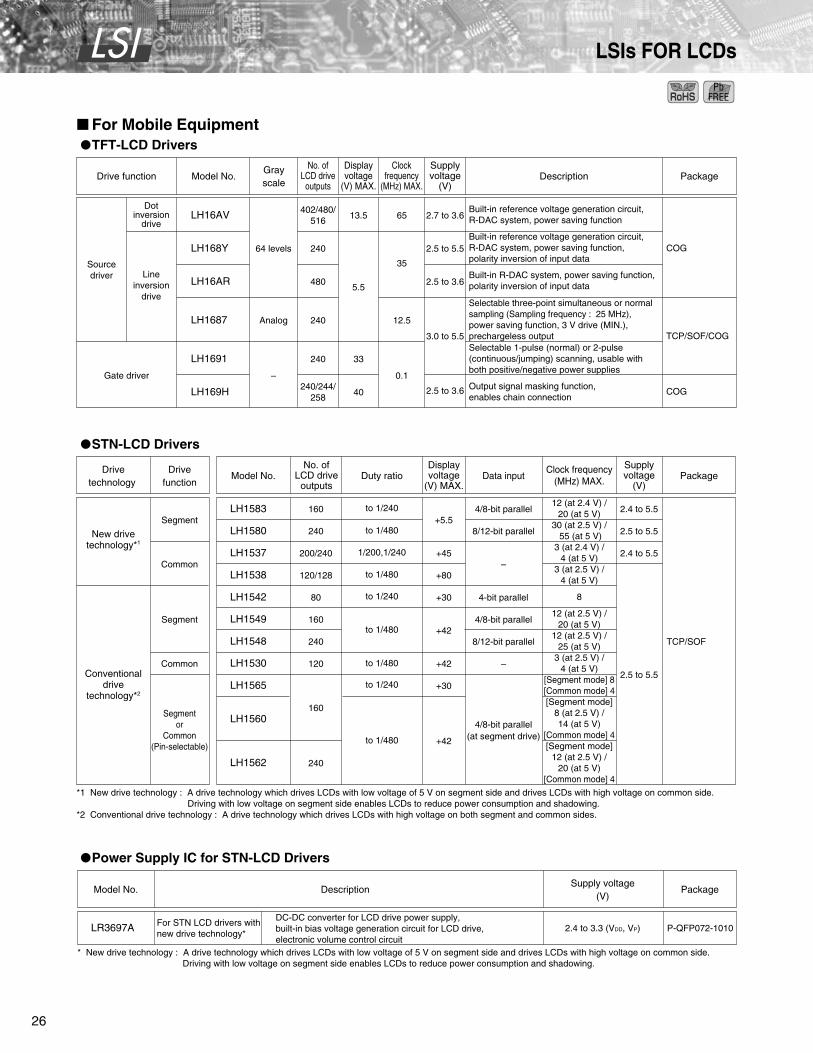
LSI
26
LSIs FOR LCDs
For Mobile Equipment
TFT-LCD Drivers
STN-LCD Drivers
Power Supply IC for STN-LCD Drivers
COG
COG
TCP/SOF/COG
13.5
5.5
33
40
65
35
12.5
0.1
240
480
240
240
402/480/516
240/244/258
LH16AV
LH168Y
LH16AR
LH1687
LH1691
LH169H
Drive function Model No.Grayscale
No. ofLCD drive
outputs
Clockfrequency
(MHz) MAX.PackageDescription
Displayvoltage
(V) MAX.
Supplyvoltage
(V)
2.7 to 3.6
2.5 to 5.5
2.5 to 3.6
3.0 to 5.5
2.5 to 3.6
Gate driver
64 levels
Analog
–
Selectable 1-pulse (normal) or 2-pulse(continuous/jumping) scanning, usable with both positive/negative power supplies
Built-in reference voltage generation circuit, R-DAC system, power saving function, polarity inversion of input data
Built-in reference voltage generation circuit, R-DAC system, power saving function
Built-in R-DAC system, power saving function, polarity inversion of input data
Output signal masking function,enables chain connection
Selectable three-point simultaneous or normalsampling (Sampling frequency : 25 MHz), power saving function, 3 V drive (MIN.), prechargeless output
Sourcedriver Line
inversiondrive
Dotinversion
drive
2.4 to 5.5
2.5 to 5.5
2.4 to 5.5
2.5 to 5.5
TCP/SOF
+5.5
+45
+80
+30
+42
+42
+30
+42
160
240
200/240
120/128
80
160
240
120
160
240
LH1583
LH1580
LH1537
LH1538
LH1542
LH1549
LH1548
LH1530
LH1565
LH1560
LH1562
to 1/240
to 1/480
to 1/480
to 1/240
to 1/480
1/200,1/240
to 1/480
to 1/240
to 1/480
Drivetechnology
Drivefunction
Model No. Duty ratioClock frequency
(MHz) MAX.Data input PackageDisplayvoltage
(V) MAX.
Supplyvoltage
(V)
No. ofLCD drive
outputs
New drivetechnology*1
Segment
Common
Segment
Common
Segmentor
Common(Pin-selectable)
4/8-bit parallel
8/12-bit parallel
–
4-bit parallel
4/8-bit parallel
8/12-bit parallel
–
4/8-bit parallel(at segment drive)
12 (at 2.4 V) /20 (at 5 V)
30 (at 2.5 V) / 55 (at 5 V)
3 (at 2.4 V) /4 (at 5 V)
3 (at 2.5 V) /4 (at 5 V)
8
12 (at 2.5 V) /20 (at 5 V)
12 (at 2.5 V) /25 (at 5 V)
3 (at 2.5 V) /4 (at 5 V)
[Segment mode] 8[Common mode] 4[Segment mode]
8 (at 2.5 V) /14 (at 5 V)
[Common mode] 4[Segment mode]
12 (at 2.5 V) /20 (at 5 V)
[Common mode] 4
*1 New drive technology : A drive technology which drives LCDs with low voltage of 5 V on segment side and drives LCDs with high voltage on common side. Driving with low voltage on segment side enables LCDs to reduce power consumption and shadowing.
*2 Conventional drive technology : A drive technology which drives LCDs with high voltage on both segment and common sides.
Conventionaldrive
technology*2
LR3697A P-QFP072-1010
Model No. DescriptionSupply voltage
(V)Package
2.4 to 3.3 (VDD, VP)For STN LCD drivers withnew drive technology*
DC-DC converter for LCD drive power supply,built-in bias voltage generation circuit for LCD drive,electronic volume control circuit
* New drive technology : A drive technology which drives LCDs with low voltage of 5 V on segment side and drives LCDs with high voltage on common side.Driving with low voltage on segment side enables LCDs to reduce power consumption and shadowing.
#

27
LSIs FOR LCDs
For Mobile Phones
TFT-LCD Controller/Driver with Two-chip Configuration (LR38825 + LH169C)
Single-chip TFT-LCD Controller/Driver
TFT-LCD Controllers
TFT-LCD Driver
LR38825 528
–
–
240LH169C
240 x 176 x 18
–
– –
COG
26.5(MAX.)
Model No.DisplaycolorsMAX.
Functiona-Si
No. of LCDdrive outputs
Source
Supply voltage (V)
Core Host I/F DisplayGatePackage
Display RAMcapacity
(bit)
CPUinterface
Externalimage
interface
262 144colors
• Versatile graphic functions• Window display function• Write mask function• Bit built function• Built-in gray-scale
control circuit• Built-in timing generator
• Built-in DC-DC converter, VCOM generation circuit
1.65 to 1.95 1.65 to 3.6 4.75 to 5.25
80-family(8/16/18-bit
parallel,serial)
RGB :respective
6-bit parallel
2.75 to 3.3
396 176 x 132 x 18 176LR38826 COG
Model No.DisplaycolorsMAX.
Functiona-Si
No. of LCDdrive outputs
Source
Supply voltage (V)
Core Host I/F DisplayGatePackage
Display RAMcapacity
(bit)
CPUinterface
Externalimage
interface
262 144colors
• Versatile graphic functions• Window display function• Write mask function• Bit built function• Built-in gray-scale
control circuit• Built-in timing generator, DC-DC converter, VCOM generation circuit
1.65 to 1.95 1.65 to 3.6
2.75 to 3.3
80-family(8/16/18-bit
parallel,serial)
RGB :respective
6-bit parallel,YUV format
Using built-in power supply ·Source : 4.0 to 5.5 ·Gate : 20 to 27.5
TFBGA112-1010
VFBGA144-0808
–
a-Si
176 x 240 176 x 240 x 16
240 x 400 x 18
LR38822A
LR388D1
TFBGA176-0909240 x 400LR38869A
VFBGA144-0808–LR388D0
Model No.DisplaycolorsMAX.
FunctionLCD
interface(pixel) MAX.
Supply voltage (V)
Core Host I/FPackage
Display RAMcapacity
(bit)
CPUinterface
Externalimage
interface
65 536colors
• Built-in timing generator, clock generator 2.25 to 2.75 3.0 to 3.6
80-family(8/16-bit
parallel, serial)
RGB :respective
6-bit parallel
RGB :respective
8-bit parallel
262 144colors
• MDDI* compliant• Built-in IrSimple™ and IrDA functions• Main/sub LCD controller• Graphic processing
MDDI* forMSM series/
80-family(8/9/16/
18-bit parallel)• MDDI* compliant• Main/sub LCD controller• Graphic processing• Parallel bus host interface
1.65 to 1.95 1.65 to 3.6
16 770kcolors
• DAC type LCD controller• Built-in voltage generation circuit for LCD• Built-in common drive circuit• Built-in level shifter for panel control• Built-in timing generator
–
* MDDI (Mobile Display Digital Interface) : The serial interface standard developed by QUALCOMM.
LTPS*
LH16AP 240 5.5 COG/SOF
Model No. FunctionLTPS*
No. of LCDdrive outputs
Source
Supply voltage (V)
DisplayMAX.
PackageExternal image
interface
• Built-in timing generator, DC-DC converter, VCOM generation circuit
2.2 to 3.6RGB : respective
6-bit parallel
* LTPS : Low Temperature Poly-Silicon
LSIs
for
LCDs
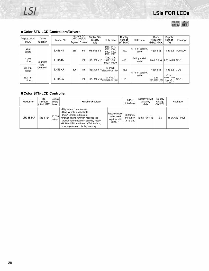
LSI
28
LSIs FOR LCDs
Color STN-LCD Controllers/Drivers
Color STN-LCD Controller
TCP/SOF
COG
COG
COG
+13.2
+18
+18.6
±18
1/10, 1/18,1/26, 1/34,1/42, 1/50,1/58, 1/66
1/33, 1/39, 1/68, 1/74,
1/133, 1/139
288
396
66
132
176
162
96 x 66 x 8
132 x 132 x 12
132 x 176 x 16
132 x 162 x 18
LH15H1
LH15JA
LH15KA
LH15LA
Segmentand
Common
4 (at 3 V)
3 (at 2.5 V)
4 (at 3 V)
1.8 to 3.3
1.65 to 3.3
1.8 to 3.3
Model NoSegment Common
PackageDuty ratio
8/16-bit parallel,serial
8-bit parallel,serial
8/16-bit parallel,serial
Data inputDisplayvoltage
(V) MAX.
Display RAMcapacity
(bit)
Clockfrequency
(MHz) MAX.
to 1/176(Selectable per 1 line)
to 1/162(Selectable per 1 line)
6.25(at 1.65 to 1.95)
Core :1.65 to 1.95
Host I/F :1.65 to 3.6
Drivefunction
Display colorsMAX.
No. of LCDdrive outputs Supply
voltage(V)
256colors
4 096colors
65 536colors
262 144colors
128 x 164 x 16 2.5 TFBGA081-0808LR38844A 128 x 164
Model No. Function/FeatureCPU
interface
LCDinterface
(pixel) MAX.
DisplaycolorsMAX.
Supplyvoltage
(V) TYP.
Display RAMcapacity
(bit)Package
Recommendedto be used
together withLH15H1
68-family/80-family(8/16 bits)
65 536colors
• High-speed host access• Display colors selectable :
256/4 096/65 536 colors• Power saving function reduces the
power consumption in standby mode • Built-in CPU interface, LCD interface,
clock generator, display memory

29
LSIs FOR LCDs
Under development
Peripheral ICs for LSIs for LCDs
Video Interface ICs for TFT-LCDs
4.5/12 or4.5/–7.5
4.5/12 or4.5/–7.5
3/12 or3/4.5/–7.5
Model No.Input signal LCD panelColor
decode
Serialdata
controlComposite
videoY/color
differenceOSD
(Digital)AnalogRGB
± powersource
+ powersource
Low voltagesource
PackageSupplyvoltage
(V) TYP.
Powerconsumption(mW) TYP.
Digitalinput
*1 For digital signal input panels*2 Built-in timing generator*3 Two inputs*4 Digital RGB input is also available.*5 At analog input for RGB
NTSC/PAL(automatic
identification)
NTSC/PAL(automatic
identification)
(Common terminal)
(Common terminal)
(Common terminal)
(Built-in)
P-QFP048-0707
P-QFP048-1010/P-QFP048-0707
P-QFP048-0707
P-QFP048-1010
P-QFP072-1010
P-QFP048-1010
P-LQFP100-1414
P-TQFP100-1414
130
140
190
160
88
106/88*5
92
70/57*5
95/80*5
120
330
250
197
257
300
5/7.5
3/12
3/6.5
3/5
3/5/13
3/7
5/13
3.3/5/7.5
3.3/5/13
3.3/5
NTSC/PAL
–
NTSC/PAL
NTSC/PAL
–
–
–
–
–
NTSC/PAL
NTSC/PAL
NTSC/PAL
NTSC/PAL
NTSC/PAL/SECAM
*3
*3
*3
*3
*4
IR3Y18A1
IR3Y26A2/A6
IR3Y29A1/B1
IR3Y31M1
IR3Y34M1
IR3Y37A1
RB5P0010M2
RB5P0020M2
RB5P0050M2
RB5P0060M2
RB5P006AM2
RB5P0070M*1
RB5P0090M
LRS5751*2
LRS5752*2
IR3Y63M
LSIs
for
LCDs
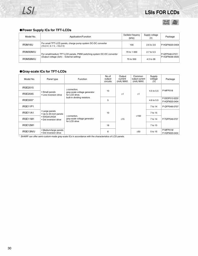
LSI
30
LSIs FOR LCDs
Power Supply ICs for TFT-LCDs
Gray-scale ICs for TFT-LCDs
P-HQFN020-0404
P-QFP048-0707/P-VQFN036-0505
IR3M16U
IR3M30M/U
IR3M58M/U
Model No. Application/Function Package
For small TFT-LCD panels, charge pump system DC-DC converter(15.3 V, 5.1 V, –10.2 V)
Supply voltage(V)
2.6 to 3.6
2.7 to 5.5
4.5 to 28
Oscillation frequency(kHz)
100
70 to 1 000
70 to 500
For small/medium TFT-LCD panels, PWM switching system DC-DC converter(Output voltage (3ch) : External setting)
P-SSOP012-0225/P-HQFN020-0404
P-QFP048-0707
P-MFP018
P-TQFP048-0707
P-MFP018/P-VQFN020-0404
±1
±15
±1
±150
±50
10
5
10
18
6
IR3E2015
IR3E2045
IR3E3XX*
IR3E11P1
IR3E11A1
IR3E11M1
IR3E12M1
IR3E13N/U
4.5 to 5.5
4.6 to 5.5
7 to 14
7 to 15
7 to 14
7 to 15
5 to 15
• Large panels• Up to 20-inch panels• SXGA/UXGA• Dot inversion drive
γ correction,gray-scale voltage generatorfor LCD drive, built-in dividing resistors
• Small panels• Line inversion drive
γ correction,gray-scale voltage generator for LCD drive
Model No. Panel type FunctionNo.ofoutputcircuits
Outputcurrent
(mA) MAX.
Common output current(mA) MAX.
Supplyvoltage
(V)Package
• Medium/large panels• Dot inversion drive
* SHARP can offer semi-custom-made gray-scale ICs in accordance with the characteristics of LCD panels.
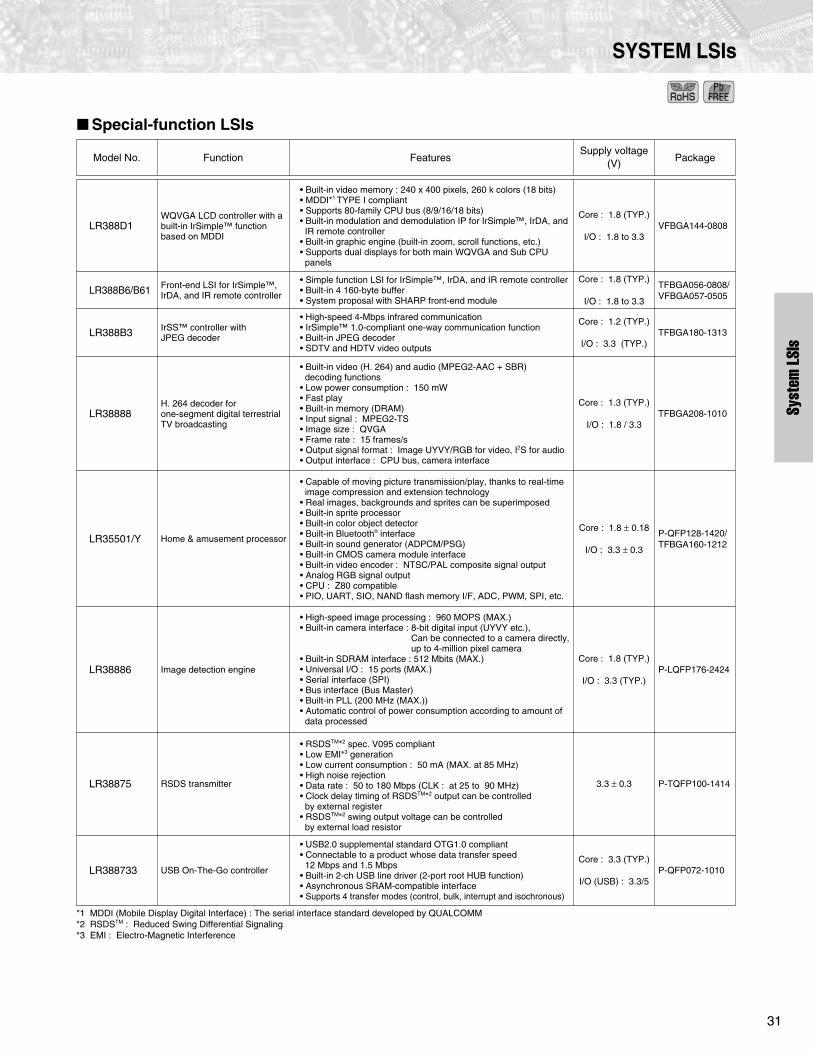
31
SYSTEM LSIs
Special-function LSIs
P-TQFP100-1414
P-QFP128-1420/TFBGA160-1212
P-QFP072-1010
TFBGA208-1010
3.3 ± 0.3
VFBGA144-0808LR388D1
LR38875
LR35501/Y
LR388733
LR38888
P-LQFP176-2424LR38886
Function Features Package
Core : 1.8 ± 0.18
I/O : 3.3 ± 0.3
Supply voltage(V)Model No.
• RSDSTM*2 spec. V095 compliant• Low EMI*3 generation• Low current consumption : 50 mA (MAX. at 85 MHz)• High noise rejection• Data rate : 50 to 180 Mbps (CLK : at 25 to 90 MHz)• Clock delay timing of RSDSTM*2 output can be controlled by external register• RSDSTM*2 swing output voltage can be controlled by external load resistor
• USB2.0 supplemental standard OTG1.0 compliant• Connectable to a product whose data transfer speed 12 Mbps and 1.5 Mbps• Built-in 2-ch USB line driver (2-port root HUB function)• Asynchronous SRAM-compatible interface• Supports 4 transfer modes (control, bulk, interrupt and isochronous)
USB On-The-Go controller
Core : 1.3 (TYP.)
I/O : 1.8 / 3.3
• Built-in video memory : 240 x 400 pixels, 260 k colors (18 bits)• MDDI*1 TYPE I compliant• Supports 80-family CPU bus (8/9/16/18 bits)• Built-in modulation and demodulation IP for IrSimple™, IrDA, and IR remote controller• Built-in graphic engine (built-in zoom, scroll functions, etc.)• Supports dual displays for both main WQVGA and Sub CPU panels
WQVGA LCD controller with abuilt-in IrSimple™ function based on MDDI
Core : 1.8 (TYP.)
I/O : 1.8 to 3.3
• Built-in video (H. 264) and audio (MPEG2-AAC + SBR) decoding functions• Low power consumption : 150 mW• Fast play • Built-in memory (DRAM) • Input signal : MPEG2-TS• Image size : QVGA • Frame rate : 15 frames/s• Output signal format : Image UYVY/RGB for video, I2S for audio• Output interface : CPU bus, camera interface
RSDS transmitter
Core : 3.3 (TYP.)
I/O (USB) : 3.3/5
H. 264 decoder for one-segment digital terrestrialTV broadcasting
TFBGA180-1313LR388B3Core : 1.2 (TYP.)
I/O : 3.3 (TYP.)
IrSS™ controller withJPEG decoder
• High-speed 4-Mbps infrared communication• IrSimple™ 1.0-compliant one-way communication function• Built-in JPEG decoder• SDTV and HDTV video outputs
Home & amusement processor
• Capable of moving picture transmission/play, thanks to real-time image compression and extension technology• Real images, backgrounds and sprites can be superimposed• Built-in sprite processor • Built-in color object detector• Built-in Bluetooth® interface• Built-in sound generator (ADPCM/PSG)• Built-in CMOS camera module interface• Built-in video encoder : NTSC/PAL composite signal output• Analog RGB signal output• CPU : Z80 compatible• PIO, UART, SIO, NAND flash memory I/F, ADC, PWM, SPI, etc.
*1 MDDI (Mobile Display Digital Interface) : The serial interface standard developed by QUALCOMM*2 RSDSTM : Reduced Swing Differential Signaling*3 EMI : Electro-Magnetic Interference
TFBGA056-0808/VFBGA057-0505
LR388B6/B61Core : 1.8 (TYP.)
I/O : 1.8 to 3.3
Front-end LSI for IrSimple™, IrDA, and IR remote controller
• Simple function LSI for IrSimple™, IrDA, and IR remote controller• Built-in 4 160-byte buffer• System proposal with SHARP front-end module
• High-speed image processing : 960 MOPS (MAX.)• Built-in camera interface : 8-bit digital input (UYVY etc.), Can be connected to a camera directly, up to 4-million pixel camera• Built-in SDRAM interface : 512 Mbits (MAX.)• Universal I/O : 15 ports (MAX.)• Serial interface (SPI)• Bus interface (Bus Master)• Built-in PLL (200 MHz (MAX.))• Automatic control of power consumption according to amount of data processed
Image detection engineCore : 1.8 (TYP.)
I/O : 3.3 (TYP.)
Syst
em LS
Is

LSI
32
IPs
The IPs contribute to shorter development time, effective use of existing software and improvement in reliability. SHARP is promoting a comprehensive range of IPs to provide support for top-down design using logic synthesis.
CPU Cores
Peripherals
Analog Cells
Analog PLL (Phase Locked Loop)
Others
ARM7TDMI
ARM720T
ARM922T
ARM946E-S
ARM926EJ-S
IP
ARM
Soft32-bit RISC ARM7TDMI CPU Core (16-bit Ins. mode supported)
ARM7TDMI + MMU + 8-Kbyte Cache
ARM9TDMI + MMU + 8-Kbyte I-cache + 8-Kbyte D-cache
ARM9E + PU + I-cache (configurable) + D-cache (configurable) + TCM (configurable)
ARM9E + MMU + I-cache (configurable) + D-cache (configurable) + TCM (configurable) + Java
MacroIP Function Data typeHard
PCMCIA1
82365SL
1284
I2C
FDC78
765A78
8051
8237A
8254
146818
8259A
8255
8251A
85C30
16550A
6402
Macro FunctionData type
Hard SoftBus Interface
PCMCIA
IEEE1284
I2C
FDD-cntl
Microcontroller & Microprocessor
8-bit-cntl
Microprocessor Peripheral
SDRAMC
DMA
LCDC
PIT
RTC
PIC
PPI
INTC
Serial Communication
USB-OTG
USART
SSP
SCC
UART
PCMCIA PC card interface
PCMCIA card interface controller
IEEE 1284 host parallel port
I2C bus interface
High performance PC compatible floppy disk controller system (82078SL)
Extended features floppy disk controller core for FM and MFM formats
High performance industry compatible 8-bit microcontroller with 2 timers
Synchronous DRAM Controller
General purpose programmable 4-channel DMA controller
Color LCD Controller (TFT, HR-TFT, CSTN, STN, DMTN)
Extended feature 3-channel Programmable Interval Timer (PIT)
Ultra-low-power real time clock with up to 114 bytes of RAM
8-channel cascadable Programmable Interrupt Controller (PIC)
General purpose Programmable Peripheral Interface (PPI)
Interrupt Controller
Universal Serial Bus On The Go Controller Full Speed (12 MHz)/Low Speed (1.5 MHz)/High Speed (480 MHz)
Universal Synchronous/Asynchronous Receiver/Transmitter (USART)
Synchronous Serial Port
SCC 2-channel Serial Communications Controller with FIFOs
Universal Asynchronous Receiver/Transmitter (UART) with FIFO
Compact Universal Asynchronous Receiver/Transmitter (UART)
IP
ADC
DAC
Macro FunctionData type
Hard SoftHigh Speed ADC
Voice ADC
Audio ADC
High Speed DAC
Voice DAC
Audio DAC
8-bit AD (80 MHz), 10-bit AD (80 MHz), 6-bit AD (80 MHz)
12-bit AD/14-bit AD (8 to 32 kHz)
20-bit AD (44.1 kHz)
8-bit DA/9-bit DA (30 MHz)
10-bit DA (8 to 32 kHz)
20-bit DA (44.1 kHz)
IP
PLLPLL
Fout : 100 to 200 MHz
Fout : 200 to 400 MHz
Fout : 400 to 800 MHz
Fin : 32 kHz, Fout : 33 to 134 MHz
IP
LVDS
RSDS
Macro FunctionData type
Hard SoftInput signal : 7-bit 3 ch (6 bits for RGB), 85 MHz (MAX.)
Input signal : 7-bit 4 ch (8 bits for RGB), 85 MHz (MAX.)
Input signal : 8 bits for RGB, 90 MHz (MAX.)
LVDS Receiver
RSDS Transmitter
Contact a SHARP sales office about applicable series. A use-fee and license-fee are required for use of the above IPs.
IP

33
SMART CARD SYSTEMS
Under development
Smart Cards/LSI Modules for Smart Cards
19.2
424
76.8
424
76.8
424
T = 1
ISO/IEC14443-4
T = 0, 1
ISO/IEC14443-4
T = 0, 1
ISO/IEC14443-4
JCOP*
TypeCommunication
standardsProtocol
Transmissionspeed
(kbps) MAX.
Nonvolatilememorycapacity
Cyclingcapability
Security systemCPU
ISO/IEC7816
ISO/IEC14443Type B
ISO/IEC7816
ISO/IEC14443Type B
ISO/IEC7816
ISO/IEC14443Type B
16 bits
16 bits
32-bit MIPS (Under development)(Under
development)
Contact
Contactless
Contact
Contactless
Contact
Contactless
RSA, DES, T-DES, etc.high-speed cryptographic authentication with built-in coprocessor,hardware-based random number generator
1 Mbyte(Flash memory)
100 000times
100 000times
100 000times
1 Mbyte(Flash memory)
1 Mbyte(Flash memory)
SJ card211• Java CardTM 2.1.1 compliance• Capable of developing applications
using Java language
JCOP* card• Java CardTM 2.2 compliance• GP (Global Platform) 2.1.1 compliance• EMV 2000 compliance• Capable of developing applications
using Java language
32-bit MIPS card• With built-in 32-bit MIPS on CPU• Security upgrades thanks to secure
controller, MIPS32TM 4KSdTM
*JCOP : JCOP means IBM's Java Card Open Platform, which was developed by IBM Corporation as an embedded Operating System (OS) for smart cards which conforms to the standards of Java and Global Platform. This platform ensures the security of applications working on various mobile terminals, such as a USB key and a smart card suitable for multiple applications.
SJCard 211
Smar
t Car
d Sy
stem
s

LSI
34
SMART CARD SYSTEMS
Reader/Writer for Smart Cards
SDK (Software Development Kit) for Smart Cards
70.4 x 14.1 x 60.5
54 x 5 x 85.6
ISO/IEC7816(T = 0, 1)
ISO/IEC7816(T = 0, 1)
RW-4040
RW-4020(LR550R03)
RW-4040•••
RW-4020 (LR550R03)••
Contact type reader/writer
High-speed data communication Conforms to PC/SC standard USB interface
Contact type reader/writer
High-speed data communication PC card interface Type II
Type
Transmission speedbetween
smart card and RW(kbps)
Smart cardoperationmethod
Outline dimensionsW x H x D
(mm)
Communicationstandard
HostinterfaceModel No.
Mass(g)
Powersupply
USB1.1
PC cardinterfaceType II
9.6 to 153.6
10.8 to 344.1
DC 5 V(USB
connector)Approx. 65
Approx. 30
Contact type
Manualinsertion/Manualejection DC 5 V
(PC cardconnector)
SDK type Contents
For SJCard 211Development kit CD for SJCardSJCard simulatorContact type reader/writer (1 set)
For JCOP Development kit CD for JCOP31id Card
!
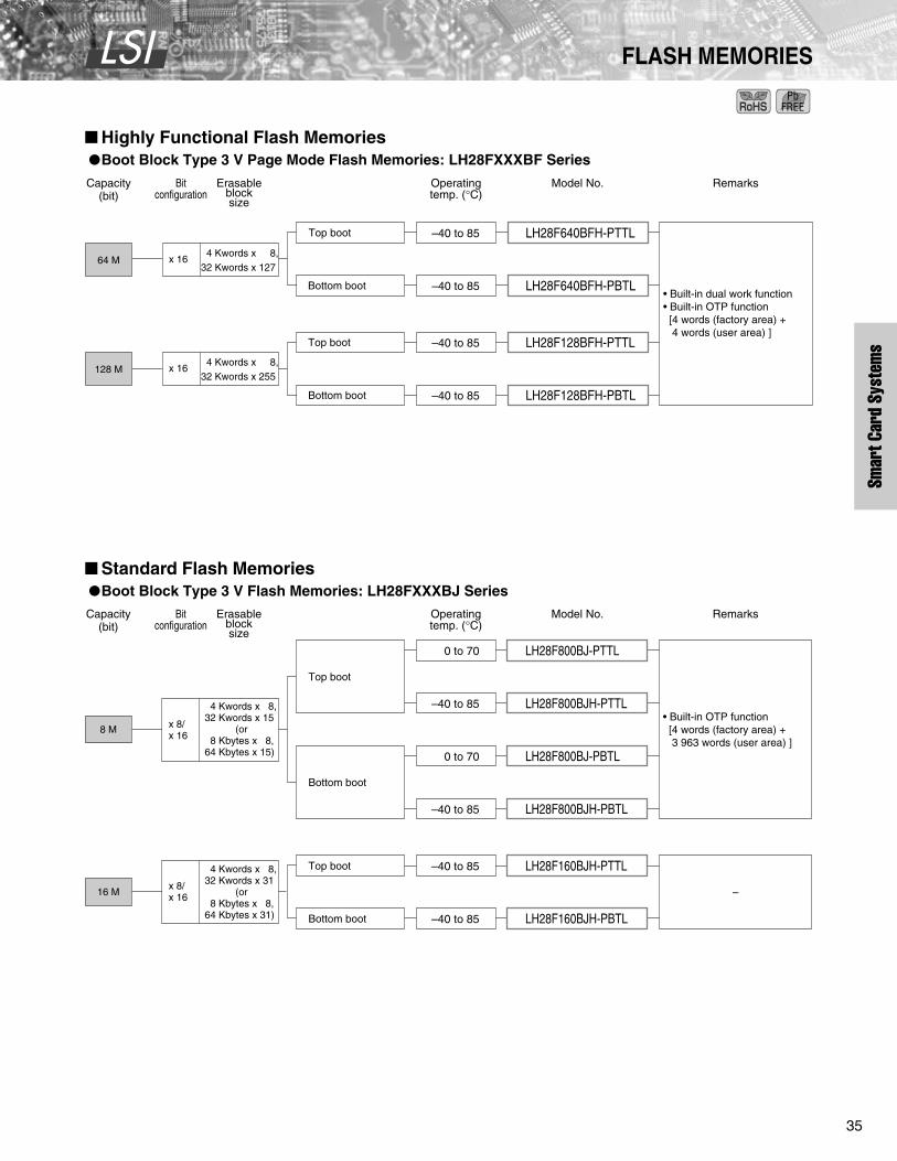
LSI
35
FLASH MEMORIES
Highly Functional Flash Memories
Boot Block Type 3 V Page Mode Flash Memories: LH28FXXXBF Series
Standard Flash Memories
Boot Block Type 3 V Flash Memories: LH28FXXXBJ Series
Capacity(bit)
Bitconfiguration
Erasableblocksize
Operatingtemp. (°C)
Model No. Remarks
• Built-in dual work function• Built-in OTP function [4 words (factory area) + 4 words (user area) ]
Top boot
Bottom boot
4 Kwords x 8,32 Kwords x 127
4 Kwords x 8,32 Kwords x 255
–40 to 85
–40 to 85
–40 to 85
–40 to 85
Top boot
Bottom boot
64 M x 16
x 16
LH28F640BFH-PBTL
128 M
LH28F128BFH-PTTL
LH28F128BFH-PBTL
LH28F640BFH-PTTL
0 to 70
–40 to 85
0 to 70
Top boot
Top boot
Bottom boot
–40 to 85
–40 to 85
–40 to 85
Bottom boot
4 Kwords x 8,32 Kwords x 15 (or 8 Kbytes x 8,64 Kbytes x 15)
4 Kwords x 8,32 Kwords x 31 (or 8 Kbytes x 8,64 Kbytes x 31)
Capacity(bit)
Bitconfiguration
Erasableblocksize
Operatingtemp. (°C)
Model No. Remarks
• Built-in OTP function [4 words (factory area) + 3 963 words (user area) ]
8 M x 8/x 16
x 8/x 1616 M
LH28F800BJ-PTTL
LH28F800BJH-PTTL
LH28F800BJ-PBTL
LH28F800BJH-PBTL
LH28F160BJH-PBTL
LH28F160BJH-PTTL
–
Smar
t Car
d Sy
stem
s
"

LSI
36
SYSTEM-FLASH
Fast-Reprogramming System-Flash for Digital Equipment
System-Flash for Amusement Products
Bitconfiguration
Erasableblocksize
Operatingtemp. (°C)
Model No.
–40 to 85
–40 to 85
Top boot
Bottom boot
Remarks
4 Kwords x 8+ 32 Kwords x 1, 64 Kwords x 15
• Fast-programming (4-Kword blocks)• Built-in OTP function [4 words (factory area) + 4 words (user area) ]–40 to 85
–40 to 85
Top boot
Bottom boot
4 Kwords x 8+ 32 Kwords x 1, 64 Kwords x 31
Capacity(bit)
LHF00L24
LHF00L28
16 M
LHF00L25
LHF00L29
x 16
LHF00L08
LHF00L10
32 M
LHF00L14
LHF00L09
LHF00L11
LHF00L15
x 16
Capacity(bit)
Bitconfiguration
Operatingtemp. (°C)
Model No. Remarks
0 to 70
0 to 70
Top boot
Top/Top boot
4 Kwords x 8,32 Kwords x 127
• 44 SOP industry standard package
0 to 85 Top boot16 Kwords x 4,64 Kwords x 255
• 70 SSOP industry standard package
• 70 SSOP industry standard package
• Compact FBGA (CSP) package
0 to 85
16 Kwords x 4,64 Kwords x 255 x 2
Erasableblocksize
0 to 70 Top boot 4 Kwords x 8+ 32 Kwords x 1, 64 Kwords x 31
• 44 SOP industry standard package
64 M
512 M
x 16
256 M x 16
x 16
32 M
LH28F640BF-PTTL
LH28F512BFBD-PTSL
LH28F256BF-PTSL
LH28F512BFND-PTSL
LHF00L34x 16
#

LSI
37
SYSTEM-FLASH
System-Flash for Automotive Use
System-Flash for Network Equipment
Capacity(bit)
Bitconfiguration
Operatingtemp. (°C)
Model No. RemarksErasableblocksize
–40 to 85
• Employs copper frame
Top boot 4 Kwords x 8,32 Kwords x 63
–40 to 85
Top boot
Bottom boot
4 Kwords x 8,32 Kwords x 127
–40 to 85 Top boot
Top/Bottom boot
4 Kwords x 8,32 Kwords x 255
x 2 4 Kwords x 8,32 Kwords x 127
–40 to 85 Top/Top bootx 2 4 Kwords x 8,32 Kwords x 255
32 M
64 M
128 M
256 M
x 16
x 16
x 16
x 16
x 16
LH28F320BFH-PTTL
LH28F640BFH-PTTL
LH28F640BFH-PBTL
LH28F128BFH-PTTL
LH28F128BFH-PWTL
LH28F256BFH-PTTL
Capacity(bit)
Bitconfiguration
Operatingtemp. (°C)
Model No. RemarksErasableblocksize
• 56 TSOP industry standard package
• 56 TSOP industry standard package
64 Kwords x 64or128 Kbytes x 64
64 Kwords x 128or128 Kbytes x 128
64 Mx 8/x 16
x 8/x 16
128 M
–40 to 85Symmetrical block LH28F640SPH-PL
–40 to 85Symmetrical block LH28F128SPH-PTL
Flash
Mem
orie
s/Co
mbi
natio
n M
emor
ies
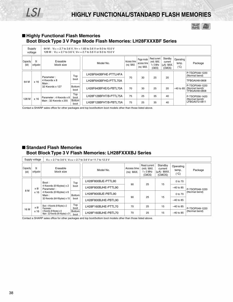
LSI
38
HIGHLY FUNCTIONAL/STANDARD FLASH MEMORIES
Highly Functional Flash MemoriesBoot Block Type 3 V Page Mode Flash Memories: LH28FXXXBF Series
Standard Flash Memories Boot Block Type 3 V Flash Memories: LH28FXXXBJ Series
TFBGA048-080820
20
40
40
25
25
35
35
30
30
25
25
70
70
75
75
LH28F640BFHE-PTTLHFA
LH28F640BFHG-PTTL70A
LH28F640BFHE/G-PBTL70A
LH28F128BFHT/B-PTTL75A
LH28F128BFHT/B-PBTL75A
64 M x 16
128 M x 16
Capacity(bit)
Bit configuration
Operatingtemp.(°C)
Erasableblock size Model No. Package
Supplyvoltage
64 M : VCC = 2.7 to 3.6 V, VPP = 1.65 to 3.6 V or 9.0 to 10.0 V128 M : VCC = 2.7 to 3.6 V, VPP = 2.7 to 3.6 V or 9.0 to 10.0 V
Access time(ns) MAX.
Page modeaccess time(ns) MAX.
Read current(mA) MAX.f = 5 MHz(CMOS)
Standbycurrent
(µA) MAX.(CMOS)
Contact a SHARP sales office for other packages and top boot/bottom boot models other than those listed above.
Parameter : 4 Kwords x 8Main : 32 Kwords x 127
Topboot
Bottomboot –40 to 85
P-TSOP048-1220(Normal bend)
P-TSOP048-1220(Normal bend)/TFBGA048-0808
P-TSOP056-1420(Normal bend)/LFBGA072-0811
Parameter : 4 Kwords x 8Main : 32 Kwords x 255
Topboot
Bottomboot
25
25
25
25
15
15
15
15
90
90
70
70
LH28F800BJE-PTTL90
LH28F800BJHE-PTTL90
LH28F800BJE-PBTL90
LH28F800BJHE-PBTL90
LH28F160BJHE-PTTL70
LH28F160BJHE-PBTL70
8 Mx 8/x 16
x 8/x 16
16 M
Capacity(bit)
Bit configuration
Operatingtemp.(°C)
Erasableblock size Model No. Package
Access time(ns) MAX.
Read current(mA) MAX.f = 5 MHz(CMOS)
Standbycurrent
(µA) MAX.(CMOS)
Contact a SHARP sales office for other packages and top boot/bottom boot models other than those listed above.
Supply voltage VCC = 2.7 to 3.6 V, VCCW = 2.7 to 3.6 V or 11.7 to 12.3 V
Topboot
Topboot
Bottomboot
Bottomboot
Boot : 4 Kwords (8 Kbytes) x 2Parameter : 4 Kwords (8 Kbytes) x 6Main : 32 Kwords (64 Kbytes) x 15
Boot : 4 Kwords (8 Kbytes) x 2Parameter : 4 Kwords (8 Kbytes) x 6Main : 32 Kwords (64 Kbytes) x 31
0 to 70
–40 to 85
0 to 70
–40 to 85
–40 to 85
–40 to 85
P-TSOP048-1220 (Normal bend)
P-TSOP048-1220 (Normal bend)
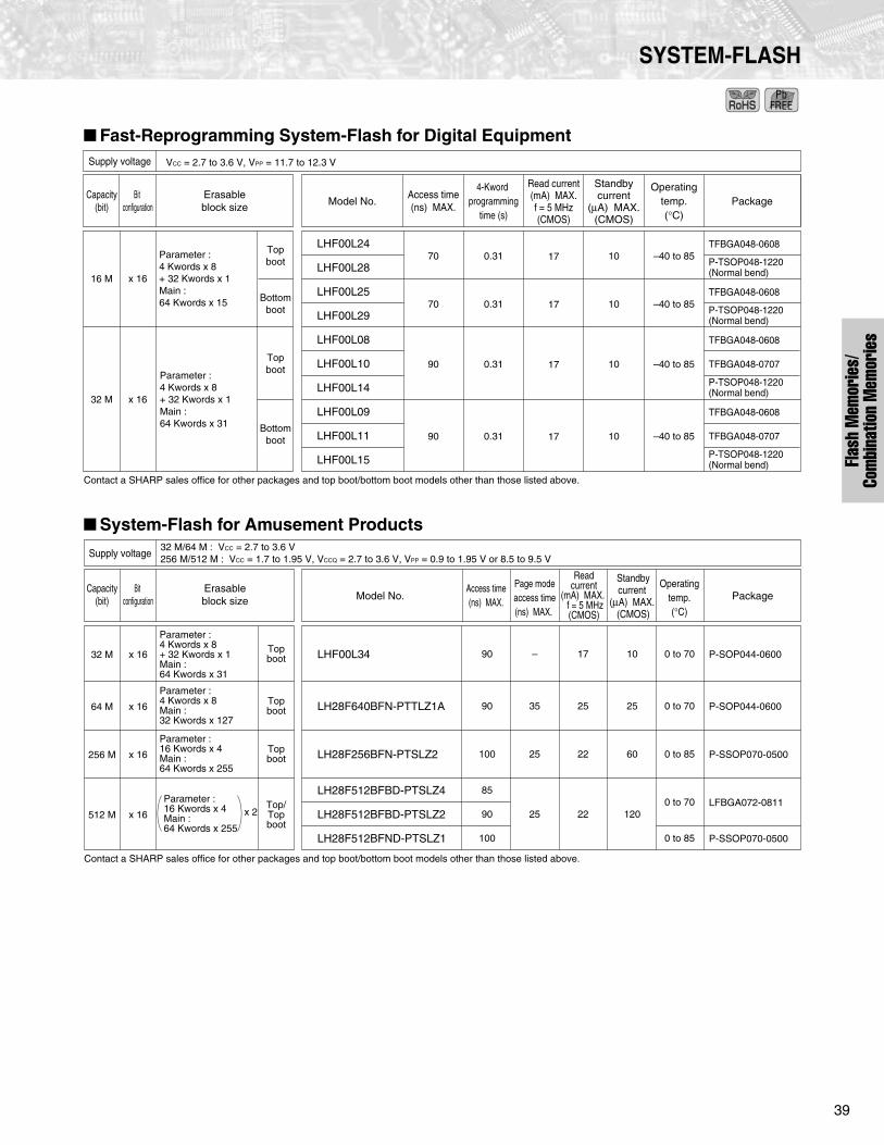
39
SYSTEM-FLASH
Fast-Reprogramming System-Flash for Digital Equipment
System-Flash for Amusement Products
10
10
10
10
17
17
17
17
70
70
90
90
0.31
0.31
0.31
0.31
LHF00L24
LHF00L28
LHF00L25
LHF00L29
LHF00L08
LHF00L10
LHF00L14
LHF00L09
LHF00L11
LHF00L15
x 1632 M
16 M x 16
Contact a SHARP sales office for other packages and top boot/bottom boot models other than those listed above.
Bottomboot
Topboot
Parameter : 4 Kwords x 8+ 32 Kwords x 1Main : 64 Kwords x 31
Capacity(bit)
Bit configuration
Operatingtemp.(°C)
Erasableblock size Model No. Package
Access time(ns) MAX.
Read current(mA) MAX.f = 5 MHz(CMOS)
4-Kword programming
time (s)
Standbycurrent
(µA) MAX.(CMOS)
Topboot
Bottomboot
Parameter : 4 Kwords x 8+ 32 Kwords x 1Main : 64 Kwords x 15
TFBGA048-0608
P-TSOP048-1220(Normal bend)
TFBGA048-0608
P-TSOP048-1220(Normal bend)
TFBGA048-0608
TFBGA048-0707
P-TSOP048-1220(Normal bend)
TFBGA048-0608
TFBGA048-0707
P-TSOP048-1220(Normal bend)
–40 to 85
–40 to 85
–40 to 85
–40 to 85
Supply voltage VCC = 2.7 to 3.6 V, VPP = 11.7 to 12.3 V
Bit configuration
Operatingtemp.(°C)
Erasableblock size Model No. Package
Supply voltage32 M/64 M : VCC = 2.7 to 3.6 V 256 M/512 M : VCC = 1.7 to 1.95 V, VCCQ = 2.7 to 3.6 V, VPP = 0.9 to 1.95 V or 8.5 to 9.5 V
Access time(ns) MAX.
Page modeaccess time(ns) MAX.
Readcurrent
(mA) MAX. f = 5 MHz(CMOS)
Standbycurrent
(µA) MAX. (CMOS)
Capacity(bit)
Topboot
Top/Topboot
Parameter :4 Kwords x 8Main : 32 Kwords x 127
Topboot
Parameter :16 Kwords x 4Main : 64 Kwords x 255
Topboot
Parameter :4 Kwords x 8+ 32 Kwords x 1Main : 64 Kwords x 31
Parameter :16 Kwords x 4Main : 64 Kwords x 255
0 to 70
0 to 70
0 to 85
0 to 70
0 to 85
Contact a SHARP sales office for other packages and top boot/bottom boot models other than those listed above.
P-SOP044-0600
P-SOP044-0600
P-SSOP070-0500
LFBGA072-0811
P-SSOP070-0500
90
90
100
85
90
100
–
35
25
25
17
25
22
22
10
25
60
120
LHF00L34
LH28F640BFN-PTTLZ1A
LH28F256BFN-PTSLZ2
LH28F512BFBD-PTSLZ4
LH28F512BFBD-PTSLZ2
LH28F512BFND-PTSLZ1
64 M x 16
256 M x 16
32 M x 16
512 M x 16 x 2
Flash
Mem
orie
s/Co
mbi
natio
n M
emor
ies

LSI
40
SYSTEM-FLASH
System-Flash for Automotive Use
System-Flash for Network Equipment
25
25
25
35
25
40
25
30
30
25
30
25
20
20
20
40
40
80
70
70
70
75
70
75
LH28F320BFHE-PTTLE0
LH28F640BFHE-PTTLH1A
LH28F640BFHE-PBTLHK
LH28F128BFHT-PTTLT1A
LH28F128BFHED-PWTLT2
LH28F256BFHTD-PTTLZ3
32 M x 16
64 M x 16
128 M x 16
256 M x 16
Capacity(bit)
Bit configuration
Operatingtemp.(°C)
Erasableblock size Model No. Package
Accesstime(ns)
MAX.
Readcurrent(mA)MAX.
f = 5 MHz(CMOS)
Pagemode
accesstime(ns)
MAX.
Standbycurrent
(µA)MAX.
(CMOS)
Supply voltage VCC = 2.7 to 3.6 V, VCCQ = 2.7 to 3.6 V
Parameter : 4 Kwords x 8Main : 32 Kwords x 63
Topboot
–40 to 85
–40 to 85
–40 to 85
–40 to 85
–40 to 85
–40 to 85
P-TSOP048-1220 (Normal bend)
Parameter : 4 Kwords x 8Main : 32 Kwords x 127
Topboot
P-TSOP048-1220 (Normal bend)Parameter :
4 Kwords x 8Main : 32 Kwords x 127
Bottomboot
Parameter : 4 Kwords x 8Main : 32 Kwords x 255
Topboot
P-TSOP056-1420 (Normal bend)
Parameter : 4 Kwords x 8Main : 32 Kwords x 127
x 2
Parameter : 4 Kwords x 8Main : 32 Kwords x 255
x 2
Top/Bottom
boot
P-TSOP048-1220 (Normal bend)
Top/Topboot
P-TSOP056-1420 (Normal bend)
1525 120120
1525 120120
LH28F640SPHT-PL12B
LH28F128SPHT-PTL12B
64 M
128 Mx 8/x 16
x 8/x 16
Capacity(bit)
Bit configuration
Operatingtemp.(°C)
Erasableblock size Model No. Package
Accesstime(ns)
MAX.
Readcurrent(mA)MAX.
f = 5 MHz(CMOS)
Pagemode
accesstime(ns)
MAX.
Standbycurrent
(µA)MAX.
(CMOS)
Supply voltage VCC = 2.7 to 3.6 V, VPP = 2.7 to 3.6 V or 9.0 to 10.0 V
64 Kwords x 64or
128 Kbytes x 64
64 Kwords x 128or
128 Kbytes x 128
Symmetricalblock
Symmetricalblock
–40 to 85
–40 to 85
P-TSOP056-1420
P-TSOP056-1420
!

41
COMBINATION MEMORIES
Under development
Boot Block Type Flash Memory + Pseudo SRAM
1.8 V models with 1.8 V I/O voltage
1.8 V models with 3 V I/O voltage
3 V models with 3 V I/O voltage
LFBGA072-0811
LFBGA072-0811
LFBGA072-0811
LFBGA088-0912
LFBGA072-0811
–
–
83 MHz
–
85
85
93
85
64 M [x 16]
128 M [x 16]
128 M [x 16]
256 M [x 16]
64 M [x 16]
25
25
25
25
70
70
70
70
20
20
20
20
–
–
52 MHz
–
256 M[x 16]
512 M [x 16]
740 M [x 16]
128 M [x 16]
LRS1890A
LRS18A6
LRS1897
LRS18CCA
LRS18CP
Model No. PackageFlash
memory
Flash memory Flashmemory
core voltageRandom
mode
PseudoSRAM
Pseudo SRAMFlash memory
blockconfiguration
Capacity (bit)[Bit configuration] Access time (ns) MAX. Supply voltage (V)
Pagemode
Synchronousburst mode
Randommode
Pagemode
Synchronousburst mode
PseudoSRAM
core voltage
I/Ovoltage
Bottom boot
Bottom boot
1.7 to 1.95
1.7 to 1.9
1.7 to 1.9
1.7 to 1.95
1.7 to 1.95
1.7 to 1.95
2.7 to 3.1
2.7 to 3.1
1.7 to 1.95
1.7 to 1.95
1.7 to 1.95
1.7 to 1.9
1.7 to 1.9
1.7 to 1.95
1.7 to 1.95
Bottom/Topboot
Bottom/Top/Bottom boot
LFBGA088-0811
LFBGA072-0811
LFBGA088-0811
LFBGA088-0811
LFBGA072-0811
LFBGA072-0811
54 MHz
–
54 MHz
54 MHz
–
65
65
20
20
–
–
85
85
25
25
85 25 – 65 20 – 1.7 to 1.95 2.7 to 3.1 2.7 to 3.1
128 M[x 16]
256 M[x 16]
32 M[x 16]
64 M [x 16]
16 M [x 16]64 M [x 16]
64 M[x 16]
LRS18CJ
LRS18CK
LRS18BK
LRS18BL
LRS18C8C
LRS18BN
LRS18AZ*
LRS18B0*
* This flash memory is divided into two banks, each including an enable signal.
Model No. PackageFlash
memory
Flash memory Flashmemory
core voltageRandom
mode
PseudoSRAM
Pseudo SRAMFlash memory
blockconfiguration
Capacity (bit)[Bit configuration] Access time (ns) MAX. Supply voltage (V)
Pagemode
Synchronousburst mode
Randommode
Pagemode
Synchronousburst mode
PseudoSRAM
core voltage
I/Ovoltage
Top boot
Bottom boot
Top boot
Bottom boot
1.7 to 1.95
1.7 to 1.95
2.7 to 3.1
2.7 to 3.1
2.7 to 3.1
2.7 to 3.1
LFBGA072-0811
LFBGA072-0811
LFBGA072-0811
85
85
70
–
35
35
–
–
–
–
–
–
85
85
60
–
–
–
LRS18BT
LRS1871A
LRS1872A
LRS18831
LRS18841
32 M [x 16] 8 M [x 16]
16 M[x 16]
64 M[x 16]
32 M[x 16]
Model No. PackageFlash
memory
Flash memory Flashmemory
core voltageRandom
mode
PseudoSRAM
Pseudo SRAMFlash memory
blockconfiguration
Capacity (bit)[Bit configuration] Access time (ns) MAX. Supply voltage (V)
Pagemode
Synchronousburst mode
Randommode
Pagemode
Synchronousburst mode
PseudoSRAM
core voltage
I/Ovoltage
Bottom boot
Top boot
Bottom boot
Top boot
Bottom boot
2.7 to 3.1
2.7 to 3.3
2.7 to 3.1
2.7 to 3.1
2.7 to 3.1
2.7 to 3.1
2.7 to 3.1
2.7 to 3.1
2.7 to 3.1
Flash
Mem
orie
s/Co
mbi
natio
n M
emor
ies
!
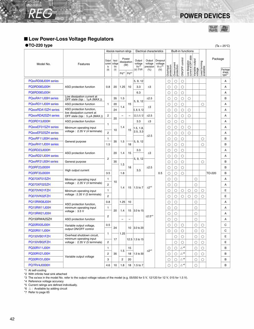
REG
42
POWER DEVICES
Low Power-Loss Voltage Regulators
TO-220 type (Ta = 25°C)
Pd*1 Pd*2
A
A
A
B
A
A
A
A
A
A
B
B
A
A
B
B
B
A
A
E
E
A
A
A
A
C
C
E
E
B
B
B
B
TO-220
o*6
o*6
o*6
o*6
±3
±2.5
±3
±2.5
±3
±2.5
±3
±2.5
±2*4
±2.5*4
±2*4
0.5
0.8
1
2
1
2
1
1.5
2
3.5
1
2
1
2
0.8
1
2
0.5
1
2
1
2
3
4.6
20
35
20
24
20
10
35
20
35
10
20
24
17
35
10
1.25
1.5
1.4
–
1.4
1.5
1.4
1.5
1.8
1.4
1.25
1.4
–
1.25
1.5
2
1.8
10
15
–
15
18
15
18
15
10
15
–
10
12.5
15
18
20
18
Features
Electrical characteristics Built-in functions
Package
Model No.
*1 At self-cooling*2 With infinite heat sink attached*3 The xx/xxx in the model No. refer to the output voltage values of the model (e.g. 05/050 for 5 V, 12/120 for 12 V, 015 for 1.5 V).*4 Reference voltage accuracy*5 Current ratings are defined individually.*6 o : Available by adding circuit*7 Refer to page 65
Lead
form
ing
avai
labl
e
Var
iabl
e ou
tput
volta
ge
Low
dis
sipa
tion
curr
ent a
t OFF
sta
te
ON
/OF
F c
ontr
ol
Ove
rcur
rent
prot
ectio
n
Ove
rhea
tpr
otec
tion
Packageshapetype*7
Absolute maximum ratings
Powerdissipation
(W)
Outputcurrent
Io(A)
Inputvoltage
Vin(V)
Outputvoltage
Vo*3
(V) TYP.
Outputvoltage
precision(%)
DropoutvoltageVI-O*5
(V)
PQxxRD08J00H series
PQ3RD083J00H
PQ6RD083J00H
PQxxRA11J00H series
PQxxRD11J00H series
PQxxxRDA1SZH series
PQxxxRDA2SZH series
PQ3RD13J000H
PQxxxEF01SZH series
PQxxxEF02SZH series
PQxxRF11J00H series
PQxxRH11J00H series
PQ3RD23J000H
PQxxRD21J00H series
PQxxRF21J00H series
PQ3RF23J000H
PQ3RF33J000H
PQ070XF01SZH
PQ070XF02SZH
PQ070VK01FZH
PQ070VK02FZH
PQ15RW08J00H
PQ15RW11J00H
PQ15RW21J00H
PQ150RWA2SZH
PQ20RX05J00H
PQ20RX11J00H
PQ150VB01FZH
PQ150VB02FZH
PQ30RV11J00H
PQ30RV21J00H
PQ30RV31J00H
PQ7RV4J0000H
ASO protection function
ASO protection function
ASO protection function
General purpose
ASO protection function
General purpose
High output current
ASO protection function
Variable output voltage
5, 9, 12
3.3
6.3
5, 9, 12
5, 8, 9, 12
3.3, 5, 9, 12
3.3
5, 9, 12
3.3
5, 9, 12
3.3
1.5 to 7
3.0 to 15
3.0 to 20
1.5 to 15
1.5 to 30
1.5 to 7
Low dissipation current at OFF state (Iqs : 1µA (MAX.))
ASO protection function,low dissipation current at OFF state (Iqs : 5 µA (MAX.))
Minimum operating inputvoltage : 2.35 V (4 terminals)
Minimum operating inputvoltage : 2.35 V (4 terminals)
Minimum operating inputvoltage : 2.35 V (5 terminals)
ASO protection function,minimum operating inputvoltage : 3.5 V
Variable output voltage,output ON/OFF control
Overheat shutdown circuit,minimum operating inputvoltage : 2.35 V (5 terminals)
1.5, 1.8,2.5, 3.3
!
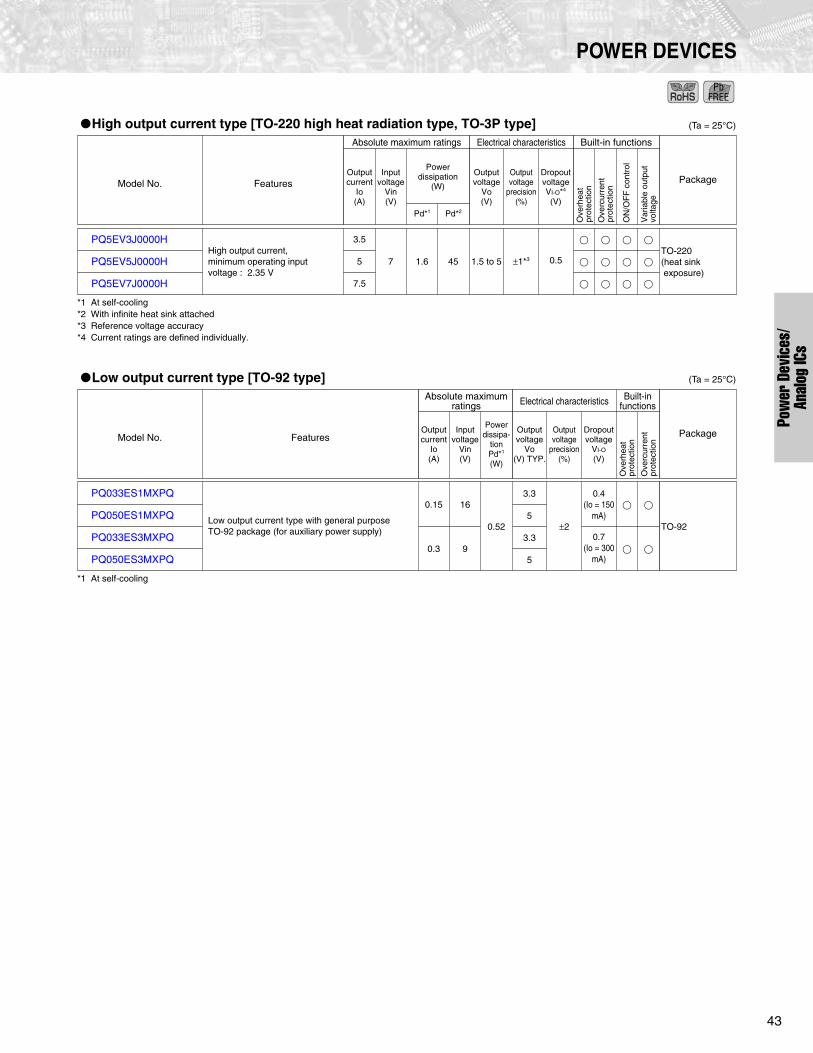
43
POWER DEVICES
High output current type [TO-220 high heat radiation type, TO-3P type]
Low output current type [TO-92 type]
(Ta = 25°C)
0.5±1*3
3.5
5
7.5
7 1.6 45
PQ5EV3J0000H
PQ5EV5J0000H
PQ5EV7J0000H
Pd*1 Pd*2
Features
Absolute maximum ratings
Powerdissipation
(W)
Electrical characteristics Built-in functions
PackageModel No.
*1 At self-cooling*2 With infinite heat sink attached*3 Reference voltage accuracy*4 Current ratings are defined individually.
Var
iabl
e ou
tput
volta
ge
ON
/OF
F c
ontr
ol
Ove
rcur
rent
prot
ectio
n
Ove
rhea
tpr
otec
tion
Outputcurrent
Io(A)
Inputvoltage
Vin(V)
Outputvoltage
Vo(V)
Outputvoltage
precision(%)
DropoutvoltageVI-O*4
(V)
High output current,minimum operating inputvoltage : 2.35 V
1.5 to 5TO-220(heat sink exposure)
(Ta = 25°C)
TO-92
0.7(Io = 300
mA)
0.4(Io = 150
mA)0.15
0.3
16
9
0.52
3.3
5
3.3
5
±2
PQ033ES1MXPQ
PQ050ES1MXPQ
PQ033ES3MXPQ
PQ050ES3MXPQ
Features PackageModel No.
Absolute maximumratings Electrical characteristics Built-in
functions
Ove
rcur
rent
prot
ectio
n
Ove
rhea
tpr
otec
tion
Outputvoltage
Vo(V) TYP.
Outputvoltage
precision(%)
Dropoutvoltage
VI-O
(V)
Low output current type with general purposeTO-92 package (for auxiliary power supply)
Outputcurrent
Io(A)
Inputvoltage
Vin(V)
Powerdissipa-
tionPd*1
(W)
*1 At self-cooling
Pow
er D
evic
es/
Anal
og IC
s
!

REG
44
POWER DEVICES
New product
Surface Mount Type Low Power-Loss Voltage Regulators
SOT-23-5 type
SOT-23L type
SOT-89 type
(Ta = 25°C)
*1 When mounted on a board*2 The xx in the model No. refer to the output voltage values of the model (e.g. 50 for 5.0 V, 18 for 1.8 V).*3 1.5, 1.8, 2.5, 2.6, 2.7, 2.8, 2.9, 3.0, 3.3, 3.5, 3.7, 4.0, 4.5, 5.0 *4 1.5, 1.8, 2.5, 3.0, 3.3, 5.0
Features
Electrical characteristics Built-in functions
PackageModel No.
Low
diss
ipat
ion
curre
nt a
t OFF
sta
te
ON
/OF
F c
ontr
ol
Ove
rcur
rent
pr
otec
tion
Ove
rhea
t pr
otec
tion
Inputvoltage
Vin(V)
Powerdissipa-
tionPd*1
(W)
Outputcurrent
Io(A)
Output voltageVo*2
(V) TYP.
Outputvoltage
precision(%)
Dropoutvoltage
VI-O
(V)
Absolute maximumratings
PQ1Uxx1M2ZPH series
PQ1Xxx1M2ZPH series
PQ1XAxx1MZPH series
± 2.0(3.0 V output)
Compact,ceramic capacitor compatibleCompact, ceramic capacitor compatible, high reliability
Compact, low output current
SOT-23-5
0.26(Io =
60 mA)
1.8, 2.5, 2.8, 3.0,3.3, 3.5, 5.0
*3
*4
16
90.35 0.18
± 2.0
(Ta = 25°C)
SOT-23L
0.26(Io = 60 mA)
0.7(Io =
300 mA)
–
0.3
16
9
15
0.4
0.18
–
*3
1.8, 2.5, 3.0,3.3, 3.6, 5.0
1.5, 1.8, 2.5,3.3, 5.0, 9.0
*1 When mounted on a board*2 The xx in the model No. refer to the output voltage values of the model (e.g. 25 for 2.5 V, 47 for 4.7 V, 50 for 5.0 V).*3 1.8, 2.0, 2.3, 2.5, 2.7, 2.8, 2.9, 3.0, 3.2, 3.3, 3.4, 3.5, 3.7, 3.8, 4.0, 4.2, 4.4, 4.7, 4.9, 5.0, 5.2
Features
Electrical characteristics Built-in functions
PackageModel No.
Low
diss
ipat
ion
curre
nt a
t OFF
sta
te
ON
/OF
F c
ontr
ol
Ove
rcur
rent
pr
otec
tion
Ove
rhea
t pr
otec
tion
Outputcurrent
Io(A)
Inputvoltage
Vin(V)
Powerdissipa-
tionPd*1
(W)
Outputvoltage
Vo*2
(V) TYP.
Outputvoltage
precision(%)
Outputcurrent
Io(A)
Dropoutvoltage
VI-O
(V)
Absolute maximumratings
PQ1RxxJ0000H series
PQ1Kxx3M2ZPH series
PQ1KAxx3MZPH series
± 2.7(3.0 V output)
± 2.0(3.0 Voutput)
Compact, surface mount type, high ripplerejection, output current of up to 300 mACompact, surface mount type, output current of up to 300 mA, ceramic capacitor compatible
Compact, surface mount type, low dissipationcurrent at OFF state (Iqs : 0.1 µA (MAX.))
(Ta = 25°C)
SOT-89
0.7
0.7
–
–
0.4
± 2.0
± 2.0*6
± 2.0*6
± 2.0
± 2.0
± 2.0
–
1.5, 1.8, 2.5,3.0, 3.2, 3.3,
5.0
1.5, 1.8, 2.5,3.3, 5.0, 9.0
1.8, 2.5,3.3, 5.0
1.5, 1.8, 2.5,3.3, 5.0
2.5, 3.3
0.8, 1.0, 1.2
*5
0.3
0.5
0.35
0.8
0.25/ch
16
15
9
6
9
0.9
*1 When mounted on a board*2 The xx in the model No. refer to the output voltage values of the model (e.g. 25 for 2.5 V, 50 for 5.0 V). [Except PQ2Lxxx2MSPQ]*3 Current ratings are defined individually.*4 Reset detection voltage : 4.2 V, 3.8 V*5 Output voltage combination : 3.3/3.3 V, 3.3/2.5 V, 3.3/1.8 V, 3.3/1.5 V, 2.5/1.8 V, 2.5/1.5 V*6 Reference voltage accuracy
Features
Electrical characteristics Built-in functions
PackageModel No.V
aria
ble
outp
utvo
ltage
Low
diss
ipat
ion
curre
nt a
t OFF
sta
te
ON
/OF
F c
ontr
ol
Ove
rcur
rent
pr
otec
tion
Ove
rhea
t pr
otec
tion
Outputcurrent
Io(A)
Inputvoltage
Vin(V)
Powerdissipa-
tionPd*1
(W)
Outputvoltage
Vo*2
(V) TYP.
Outputvoltage
precision(%)
DropoutvoltageVI-O*3
(V)
Absolute maximumratings
PQ1Lxx3M2SPQ
PQ1LAxx3MSPQ
PQ1LAxx5MSP series
PQ1LAX95MSPQ
PQ1Mxx5M2SPQ
PQ1MX55M2SPQ
PQ1Nxx3MxSPQ
PQ1MGxx8MSPQ
PQ1MGX38MSPQ
PQ2Lxxx2MSPQ
1.5 to 9.0
0.5 to 3.5
1.3 to 5.0
± 2.0(3.0 Voutput)
± 2.0(5.0 V output)
Compact, high radiation package,low dissipation current at OFF state(Iqs : 1 µA (MAX.)), ceramiccapacitor compatible
Ceramic capacitor compatible, variable output voltageCompact, high output current, ceramic capacitor compatible
Compact, high radiation package, ceramic capacitor compatible
Compact, ceramic capacitor compatibleCompact, ceramic capacitor compatible, variable output type
Ceramic capacitor compatible, variable output voltageReset signal output function*4, ceramic capacitor compatible
Compact, high radiation package,2 outputs
Compact, high radiation package,low dissipation current at OFF state (Iqs : 1 µA (MAX.))
!!
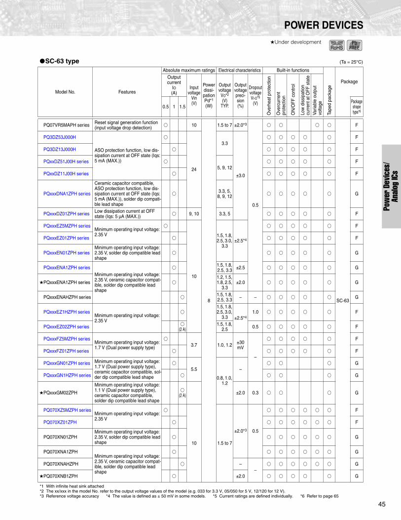
45
POWER DEVICES
Under development
SC-63 type
*1 With infinite heat sink attached*2 The xx/xxx in the model No. refer to the output voltage values of the model (e.g. 033 for 3.3 V, 05/050 for 5 V, 12/120 for 12 V).*3 Reference voltage accuracy *4 The value is defined as ± 50 mV in some models. *5 Current ratings are defined individually. *6 Refer to page 65
Model No. Features
Absolute maximum ratings
Electrical characteristics
Built-in functions
Tape
d pa
ckag
e
PackageOutput current
I
O
(A)
Input voltage
Vin (V)
Power dissi-pation Pd*
1
(W)
Output voltage
V
O
*
2
(V)
TYP.
Output voltage preci-sion (%)
Dropout voltage V
I-O
*
5
(V)
Ove
rhea
t pro
tect
ion
Ove
rcur
rent
pr
otec
tion
ON
/OFF
con
trol
Low
dis
sipa
tion
curr
ent a
t OFF
sta
te
Varia
ble
outp
ut
volta
ge0.5 1 1.5
Package shape type*
6
PQ07VR5MAPH series Reset signal generation function (input voltage drop detection)
10
8
1.5 to 7 ±2.0*
3
0.5
SC-63
F
PQ3DZ53J000H
ASO protection function, low dis-sipation current at OFF state (Iqs: 5 mA (MAX.))
24
3.3
±3.0
F
PQ3DZ13J000H
F
PQxxDZ51J00H series
5, 9, 12
F
PQxxDZ11J00H series
F
PQxxxDNA1ZPH series
Ceramic capacitor compatible, ASO protection function, low dis-sipation current at OFF state (Iqs: 5 mA (MAX.)), solder dip compati-ble lead shape
3.3, 5, 8, 9, 12
G
PQxxxDZ01ZPH series Low dissipation current at OFF state (Iqs: 5 µA (MAX.))
9, 10 3.3, 5
F
PQxxxEZ5MZPH seriesMinimum operating input voltage: 2.35 V
10
1.5, 1.8, 2.5, 3.0,
3.3±2.5*
4
F
PQxxxEZ01ZPH series
F
PQxxxEN01ZPH seriesMinimum operating input voltage: 2.35 V, solder dip compatible lead shape
G
PQxxxENA1ZPH seriesMinimum operating input voltage: 2.35 V, ceramic capacitor compat-ible, solder dip compatible lead shape
1.5, 1.8, 2.5, 3.3 ±2.5
G
PQxxxENA1ZPH series
1.2, 1.5, 1.8, 2.5,
3.3±2.0
G
PQxxxENAHZPH series
1.5, 1.8, 2.5, 3.3 – –
G
PQxxxEZ1HZPH seriesMinimum operating input voltage: 2.35 V
1.5, 1.8, 2.5, 3.0,
3.3 ±2.5*
4
1.0
F
PQxxxEZ02ZPH series
(2 A)
1.5, 1.8, 2.5 0.5
F
PQxxxFZ5MZPH seriesMinimum operating input voltage: 1.7 V (Dual power supply type)
3.7 1.0, 1.2 ±30 mV
–
F
PQxxxFZ01ZPH series
F
PQxxxGN01ZPH series Minimum operating input voltage: 1.7 V (Dual power supply type), ceramic capacitor compatible, sol-der dip compatible lead shape
5.5
0.8, 1.0, 1.2
–
G
PQxxxGN1HZPH series
G
PQxxxGM02ZPH
Minimum operating input voltage: 1.1 V (Dual power supply type), ceramic capacitor compatible, solder dip compatible lead shape
(2 A)
±2.0 0.3
G
PQ070XZ5MZPH seriesMinimum operating input voltage: 2.35 V
10 1.5 to 7
±2.0*
3
0.5
F
PQ070XZ01ZPH
F
PQ070XN01ZPHMinimum operating input voltage: 2.35 V, solder dip compatible lead shape
G
PQ070XNA1ZPHMinimum operating input voltage: 2.35 V, ceramic capacitor compat-ible, solder dip compatible lead shape
G
PQ070XNAHZPH
––
G
PQ070XNB1ZPH
±2.0
G
(Ta = 25°C)
Pow
er D
evic
es/
Anal
og IC
s
!"

REG
46
POWER DEVICES
Under development
SC-63 type (cont’d)
*1 With infinite heat sink attached*2 The xx/xxx in the model No. refer to the output voltage values of the model (e.g. 033 for 3.3 V, 05/050 for 5 V, 12/120 for 12 V).*3 Reference voltage accuracy *4 The value is defined as ± 50 mV in some models. *5 Current ratings are defined individually. *6 Refer to page 65
Model No. Features
Absolute maximum ratings
Electrical characteristics
Built-in functions
Tape
d pa
ckag
e
PackageOutput current
I
O
(A)
Input voltage
Vin (V)
Power dissi-pation Pd*
1
(W)
Output voltage
V
O
*
2
(V)
TYP.
Output voltage preci-sion (%)
Dropout voltage V
I-O
*
5
(V)
Ove
rhea
t pro
tect
ion
Ove
rcur
rent
pr
otec
tion
ON
/OFF
con
trol
Low
dis
sipa
tion
curr
ent a
t OFF
sta
te
Varia
ble
outp
ut
volta
ge0.5 1 1.5
Package shape type*
6
PQ070XZ1HZPHMinimum operating input voltage: 2.35 V
10
8
1.5 to 7 ±2.0*
3
1.0
SC-63
F
PQ070XZ02ZPH
(2 A)
0.5
F
PQ015YZ5MZPH Reference voltage (Vref): 1.0 V, minimum operating input voltage: 1.7 V (Dual power supply type)
3.7 1.0 to 1.5 ±3.0*
3
–
F
PQ015YZ01ZPH
F
PQ035ZN01ZPH Reference voltage (Vref): 0.6 V, minimum operating input voltage: 1.7 V (Dual power supply type), ceramic capacitor compatible, solder dip compatible lead shape
5.5
0.8 to 3.5
±30 mV
G
PQ035ZN1HZPH
G
PQ035ZM02ZPH
Minimum operating input voltage: 1.1 V (Dual power supply type), ceramic capacitor compatible, solder dip compatible lead shape
(2 A)
±2.0 0.3
G
PQ20VZ51J00HMinimum operating input voltage: 4.5 V
24
1.5 to 20 ±2.0*
3
0.5
F
PQ20VZ11J00H
F
PQ20WZ51J00H Minimum operating input voltage: 3.5 V, ASO protection function, low dissipation current at OFF state (Iqs: 5 µA (MAX.))
3.0 to 20 ±2.5*
3
F
PQ20WZ11J00H
F
PQ200WNA1ZPH
Minimum operating input voltage: 3.5 V, ASO protection function, low dissipation current at OFF state (Iqs: 5 µA (MAX.)) ceramic capacitor compatible, solder dip compatible lead shape
3.0 to 20
±2.5*
3
G
PQ200WN3MZPH
Minimum operating input voltage: 3.5 V, low dissipation current at OFF state (Iqs: 5 µA (MAX.)), ceramic capacitor compatible, current limit: 800 mA
(0.3)
6.8 5.0 to 20
(Ta = 25°C)
!#
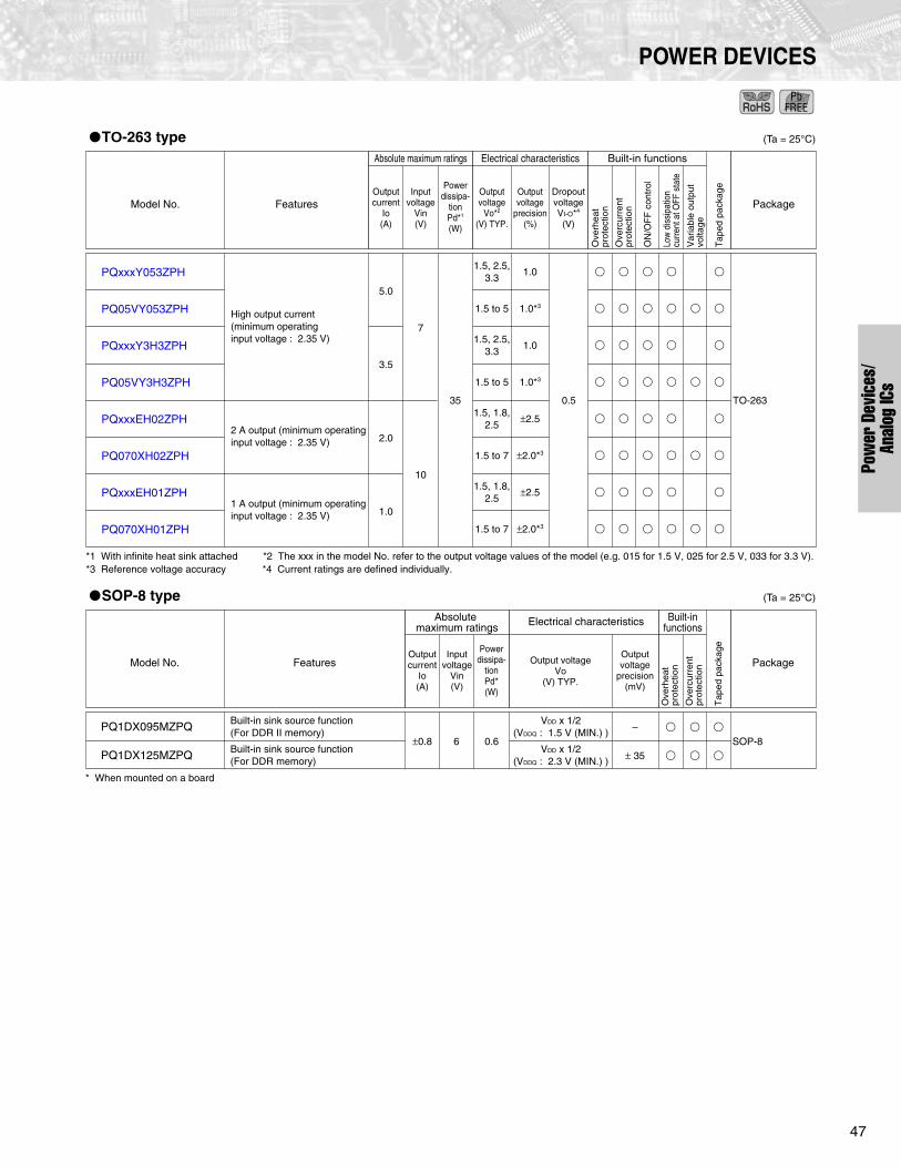
47
POWER DEVICES
TO-263 type
SOP-8 type
(Ta = 25°C)
Features
Absolute maximum ratings
Outputcurrent
Io(A)
Inputvoltage
Vin(V)
Powerdissipa-
tionPd*1
(W)
Electrical characteristics Built-in functions
PackageModel No.Outputvoltage
Vo*2
(V) TYP.
Outputvoltage
precision(%)
Tap
ed p
acka
ge
Var
iabl
e ou
tput
volta
ge
Low
dis
sipa
tion
curr
ent a
t OFF
sta
te
ON
/OF
F c
ontr
ol
Ove
rcur
rent
prot
ectio
n
Ove
rhea
tpr
otec
tion
DropoutvoltageVI-O*4
(V)
*1 With infinite heat sink attached *2 The xxx in the model No. refer to the output voltage values of the model (e.g. 015 for 1.5 V, 025 for 2.5 V, 033 for 3.3 V).*3 Reference voltage accuracy *4 Current ratings are defined individually.
High output current (minimum operating input voltage : 2.35 V)
2 A output (minimum operating input voltage : 2.35 V)
1 A output (minimum operating input voltage : 2.35 V)
1.5 to 5
1.5 to 5
1.5 to 7
1.5 to 7
TO-263
0.5
1.0
1.0*3
1.0
1.0*3
±2.5
±2.0*3
±2.5
±2.0*3
1.5, 2.5,3.3
1.5, 2.5,3.3
1.5, 1.8,2.5
1.5, 1.8,2.5
5.0
3.5
2.0
1.0
7
10
35
PQxxxY053ZPH
PQ05VY053ZPH
PQxxxY3H3ZPH
PQ05VY3H3ZPH
PQxxxEH02ZPH
PQ070XH02ZPH
PQxxxEH01ZPH
PQ070XH01ZPH
(Ta = 25°C)
SOP-8–
± 35
VDD x 1/2(VDDQ : 1.5 V (MIN.) )
VDD x 1/2(VDDQ : 2.3 V (MIN.) )
±0.8 6 0.6PQ1DX095MZPQ
PQ1DX125MZPQ
Features
Absolute maximum ratings
Outputcurrent
Io(A)
Inputvoltage
Vin(V)
Powerdissipa-
tionPd*(W)
Electrical characteristics Built-infunctions
PackageModel No. Output voltageVo
(V) TYP.
Outputvoltage
precision(mV)
Tap
ed p
acka
ge
Ove
rcur
rent
prot
ectio
n
Ove
rhea
tpr
otec
tion
* When mounted on a board
Built-in sink source function(For DDR II memory)
Built-in sink source function(For DDR memory)
Pow
er D
evic
es/
Anal
og IC
s
!

REG
48
POWER DEVICES
Under development
Surface Mount Type Chopper Regulators (DC-DC Converters) (Ta = 25°C)
SOT-23-6
SOT-23-6W
SOP-8
USB-6
USB-10
TO-263
P-SSOP008-0150
USB-6
SC-63
2 M
300 k
300 k
220 k
150 k
400 k
150 k
100 k
1.2 M
0.25*1
1.5*1
0.8*1
2.5*1
1.5*1
3.5*1
1
Input voltagerangeVin (V)
Built-inSWTr
Oscillationfrequency
fo (Hz) TYP.
OutputvoltageVo (V)
No. ofoutputcircuits
Output type
Stepdown
Stepup
Inver-sion
PackageModel No. FeaturesSwitchcurrentIsw (A)
*1 Peak current (absolute maximum ratings) *2 VREF nearly equal to 1.26 V (TYP.) *3 VREF nearly equal to 1 V (TYP.) *4 VREF nearly equal to 0.8 V (TYP.)*5 Output voltage variable range *6 The xx in the model No. refer to the output voltage values of the model (e.g. 33 for 3.3 V, 50 for 5.0 V). *7 Selectable oscillation frequency range
up to 5.5
2.7 to 5.5
3.0 to 5.5
up to 40
up to 33
up to 28
up to 40
2.2 to 6.0
4.5 to 22
—
up to 30
up to 36
up to 30
PQ6CU11X1APQ
PQ6CB11X1AP
PQ6CB11X1CP
PQ6CU12X2APQ
PQ7L2010BP
PQ1CZ38M2ZPH series
PQ1CZ21H2ZPH
PQ1CZ41H2ZPH
PQ1CX12H2ZPQ
PQ1CX22H2ZPQ
PQ1CX41H2ZPQ
PQ1CY1032ZPH
IR3M18N
IR3M19N
• High voltage CMOS output : 30 V (MAX.)• White LED driver for back light (Capable of driving up to 4 LEDs in series connection)• Output ON/OFF control function• Overvoltage/overcurrent protection circuits• Soft start function
• High voltage CMOS output : 30 V (MAX.)• White LED driver for back light (Capable of driving up to 6 LEDs in series connection)• Output ON/OFF control function• Overvoltage/overcurrent protection circuits• Soft start function
• High switching voltage : 40 V (MAX.)• For tuner power supply• Output ON/OFF control function
• Possible to correspond also to operation in the minute lighting mode• High frequecny PWM control for brightness adjustment• Output ON/OFF control function
• PWM chopper regulator (high oscillation frequency)• Output ON/OFF control function• Overcurrent/overheat protection circuits• For light load
• Bootstrap system for high efficiency (Efficiency 90% (TYP.) )• Low dissipation current
• Bootstrap system for high efficiency (Efficiency 90% (TYP.) )• Low dissipation current• Low voltage output : 1.2 V (MIN.)
• Bootstrap system for high efficiency (Efficiency 91% (TYP.) )• Low voltage output : 0.8 V (MIN.)• Ceramic capacitor compatible
• PWM chopper regulator• Output ON/OFF control function• Overheat protection/overcurrent shutdown circuits• High output current type
• PWM chopper regulator• Fixed output voltage : 3.3 V or 5 V• Output ON/OFF control function• Overheat protection circuit
• Soft start function• Undervoltage protection circuit• Timer latch short-circuit protection circuit• Standby function
• High transient load characteristics from built-in current control circuit• Soft start function• Overcurrent/overvoltage/undervoltage protection circuits• Internal reference voltage accuracy (±1%)
• High voltage CMOS output : 30 V (MAX.)• White LED driver for back light• Output ON/OFF control function• Overvoltage/overcurrent protection circuits• Soft start function
• PWM chopper regulator• Output ON/OFF control function• Overcurrent/overheat protection circuits • Low dissipation current at OFF state (Standby crrent <ISD> : 1 µA (MAX.) )
• PWM chopper regulator• Sleep mode function (by switching between PWM and PFM)• Overvoltage/overcurrent protection circuits• Soft start function
• PWM chopper regulator (high oscillation frequency)• Output ON/OFF control function• Overcurrent/overheat protection circuits
PQ1CYxx3HZPH seriesPQ1CYxx3LZPH series
(Determinedby external
Tr)
100 k to1 M*7
(Determinedby external
Tr) 1.24 toinput
voltage
Switchablebetween
2.0 M and1.2 M
300 k to800 k*7
VREF*2
to 35*5
(step-downtype)/
–VREF*2
to –30*5
(invertingtype)
VREF*2 to 35*5
(step-down type)/–VREF*2 to –30*5
(inverting type)
from 0.8
3.3, 5.0*6
(TYP.)
VREF*3
to 24*5
(step-downtype)
VREF*4
to 24*5
(step-downtype)
External
2.7 to 5.5
PQ5CB11X1AP
!

49
POWER DEVICES
Under development
Surface Mount Type Chopper Regulators (DC-DC Converters) (cont’d)
Chopper Regulators (DC-DC Converters)
TO-220 type
(Ta = 25°C)
P-HQFN020-0404
P-TSSOP028-0225
P-QFP048-0707/P-VQFN036-0505
2
1
3
IR3M17U
IR3M57N
IR3M56N
IR3M30M/U
IR3M58M/U
P-TSSOP016-0225
Built-inSWTr
Oscillationfrequency
fo (Hz) TYP.
No. ofoutputcircuits
Output type
Stepdown
Stepup
Inver-sion
PackageModel No. Features
*1 Built-in SW Tr can be used in step-up mode ; external SW Tr is required in step-down or inverting mode.*2 Constant current (MAX.)*3 Selectable oscillation frequency range
Input voltagerangeVin (V)
OutputvoltageVo (V)
SwitchcurrentIsw (A)
o*1
External
o*1
External
2.2 to 6.5
4.5 to 36
2.7 to 5.5
4.5 to 28
0.8 to 6.3
• High efficiency two channel synchronous rectified step-down converter• Current mode control• Soft start function• Overcurrent/overvoltage/undervoltage/ overheat protection circuits
• ON/OFF sequence setting • Timer latch short-circuit protection circuit• Soft start function• Overcurrent/undervoltage/overheat protection circuits
• ON/OFF sequence setting without external control• Timer latch phase fault protection circuit• Soft start function• Overcurrent/undervoltage/overheat protection circuits
(Determinedby
external Tr)
(Determinedby
external Tr)
200 k/300 k/400 k/500 k/
externalsync.
Externalsetting
0.4*2 (when using internal Tr)
Externalsetting
1*2
(when using internal Tr)
External
External
Externalsetting
70 k to1M*3
70 k to500 k*3
• Standby function (output ON/OFF control function for each channel)• Soft start function• Undervoltage protection circuit
100 k to500 k*3/
external sync.
(Determinedby external
Tr)
• High efficiency synchronous rectified step-down converter• Current mode control• Soft start function• Overcurrent/overvoltage/undervoltage/overheat protection circuits
200 k/300 k/400 k/500 k/
external sync.4.5 to 36 0.8 to 6.3
(Ta = 25°C)
E
D
E
D
E
D
E
D
E
D
E
0.9
1.0
0.9
1.4
0.6
TO-220
300
100
300
70
150
50
0.8*3
1.5*3
3.5*3
2.5*3
40
35
14
15
PQ1CG38M2FZH
PQ1CG38M2RZH
PQ1CG21H2FZH
PQ1CG21H2RZH
PQ1CG41H2FZH
PQ1CG41H2RZH
PQ1CG2032FZH
PQ1CG2032RZH
PQ1CG3032FZH
PQ1CG3032RZH
PQ2CF1J0000H
Features
Absolute maximum ratings
Switchcurrent
Isw(A)
Inputvoltage
Vin(V)
Powerdissipa-
tionPd*1
(W)
Electrical characteristics
Model No. Output voltageVo*2
(V)
Oscillationfrequencyfo (kHz)
TYP.
• PWM chopper regulator (high oscillation frequency)• Built-in overcurrent/overheat protection circuits• Output ON/OFF control function• For light load
• PWM chopper regulator• Built-in overcurrent/overheat protection circuits • Output ON/OFF control function
• PWM chopper regulator (high oscillation frequency)• Built-in overcurrent/overheat protection circuits• Output ON/OFF control function
• PWM chopper regulator• Built-in overcurrent/overheat protection circuits• Output ON/OFF control function
• PWM chopper regulator (high oscillation frequency)• Built-in overcurrent/overheat protection circuits• Output ON/OFF control function
• PWM chopper regulator• Built-in overcurrent/overheat protection circuits
VREF*4 to 35(step-down type)/
–VREF*4 to –30(inverting type)
4.5 to 35(step-up type)
*1 With infinite heat sink attached *2 Output voltage variable range *3 Peak current *4 VREF nearly equal to 1.26 V (TYP.) *5 Refer to page 65
Package
Outlineshapetype*5
Outputsaturation
voltageVsat
(V) TYP.
!

LSI
50
POWER DEVICES
Power Supply ICs for CCDs/CCD Camera Modules
Power Supply ICs for TFT-LCDs
Input voltagerange(V)
Outputvoltage
(V)
No. ofoutputcircuits
Switching frequency
(Hz)SW TrSystem PackageModel No.
Switching current (mA)
[Built-in SW Tr]
Drive capacity (pF)
[External SW Tr]
*1 For automotive use *2 3.97 mm x 3.97 mm x 0.82 mm (TYP.)
IR3M52Y7
IR3M61U*1/63U
IR3M49U6
IR3M55U*1/59U
IR3M48U6
5
4
3
2.7 to 5.5
4.5 to 10
2.7 to 5.5
4.5 to 16
2.7 to 3.2
Step-up type PWM + REG
Inverting type PWM
REG
REG
REG
Charge pump
Negative charge pump
Step-down type PWM + REG
Step-down type PWM + REG
Step-up type PWM + REG
Inverting type PWM
REG
Charge pump
Negative charge pump
Step-down type PWM + REG
Charge pump + REG
Negative charge pump + REG
REG
Built-in
External
–
–
Built-in
Built-in
External
–
–
Built-in
–
20 (DC)
–
100 (DC)
100 (DC)
100 (DC)
1.2 (DC)
2.5 (DC)
120 (DC)
50 (DC)
600 (DC)
–
–
170 (DC)
10/20 (DC)
2/5 (DC)
150 (DC)
6 (DC)
7 (DC)
50 (DC)
–
1 000
–
–
–
–
–
–
–
–
1 000
1 000
–
–
–
–
–
–
–
15
–8
2.5 to 3.3
2.5 to 3.3
1.8/1.2
15
–8
3.3
1.8
15
15/12
–8/–5
3.3
15
–8
1.8
1 M
–
200 k
1 M
1 M
–
200 k
1 M
300 k
–
P-VQFN032-0505
P-VQFN036-0505
41WL-CSP*2
P-VQFN032-0505
P-VQFN032-0505
Step-up, step-down, step-up/down type PWM
External setting
Input voltagerange(V)
Outputvoltage
(V)
No. ofoutputcircuits
Switching frequency
(Hz)SW TrSystem PackageModel No.
Switching current (mA)
[Built-in SW Tr]
Drive capacity (pF)
[External SW Tr]
IR3M58M/U
IR3M30M/U
IR3M16U
3
4.5 to 28
2.7 to 5.5
2.6 to 3.6
Step-down type PWM
Charge pump
Charge pump + REG
Negative charge pump
External
External
External
–
–
–
400
–
–
1 000
1 000
–
0.1 (DC)
5 (DC)
0.1 (DC)
1 000
–
–
1 000
–
–
–
15.3
5.1
–10.2
100 k P-HQFN020-0404
P-QFP048-0707/P-VQFN036-0505
70 k to1 M
70 k to500 k
Step-up, step-down, step-up/down type PWM
Step-down, inverting type PWM
Step-up, step-down, step-up/down, inverting type PWM
Step-up, step-down, step-up/down, inverting type PWM
Step-up (20 V (MAX.) )/ step-down type PWM
External setting
External setting
Built-in(Step-up type)
Built-in(Step-up type)
Built-in(Step-up type)
"

51
POWER DEVICES
Fail Safe IC
LED Drivers
Built-in step up circuit
Operating voltage
VBAT (V) VBAC (V) VIO (V)Features
Operating temp.(°C)
Model No.
IR3T46U/46U6*
• Malfunction detection• Built-in 8-bit ADC• Built-in timer circuit• Built-in key detection output OR gate
3.2 to 4.5 3.0 to 3.3 2.6 to 3.0 –20 to +85
Dissipation current(µA)
TYP. 10
* 46U: Tray package 46U6: Taped package
FunctionModel No.
PQ6CU11X1APQ
PQ6CB11X1AP
PQ6CB11X1CP
PQ7L2010BP
PWM
3(Series
connection)
4(Series
connection)
6(Series
connection)
4(Series
connection)
*1
*1
*1
*1
to 5.5
2.7 to 5.5
1250*2
1.2 M
2.0 M
SOT-23-6
USB-6
USB-10
• High voltage CMOS output: 30 V (MAX.)• Output ON/OFF control function• Overvoltage/overcurrent protection circuits• Softstart function
• Possible to correspond also to operation in the minute lighting mode• High frequency PWM control for brightness adjustment• Output ON/OFF control function
White LED driver for back light(for small panels)
IR2E46Y6
IR2E47U6
IR2E49U
IR2E51Y6
3
6
5 PWM
PWM3
4 + 2
40
2.7 to 4.5
2.7 to 5.5
6 to 28
20/ch
1.2 M
1 M
33WL-CSP*4
35WL-CSP*4
P-HQFN024-0404
P-VQFN036-0606
RGB LED driver for picture lights and illuminations
White LED driver for back light(for small panels)
White LED driver for back light(for mediumpanels)
LED driver for back light and call alert display LED driver(auto brightnessadjustment)
4 + 2+ 3
Chargepump
Chargepump
3.0 to 4.5(for drive)/2.3 to 3.2
(for control)
155/ch(in picture light mode)
150/ch*2
25/ch
• I2C bus control• Illumination mode (64 levels/ch)• Picture light mode (32 levels/ch)• Brightness adjustment• Standby function/soft start function• Overcurrent/undervoltage/overheat protection circuits
• Independent current control for two systems (4 outputs and 2 outputs)• LED non-connected judging function• Brightness adjustment• Undervoltage/overheat protection circuits
• Buit-in 150 mA driver for each channel• Step-up DC-DC output short-circuit protection function• Current driver output open detection• Capable of external brightness adjustment using PWM input signal• Overcurrent/overvoltage/undervoltage/ overheat protection circuits
• Capable of direct connection of ambient light sensor• Brightness adjustment by ambient illuminance feedback (16-step ambient illuminance/128-level illuminance) (for main LCDs)• Non-external coil thanks to charge pump drive• Capable of driving 4 main-LEDs, 2 sub-LEDs, and 3 call alert LEDs with a single device.• I2C interface • Standby function/power on reset function/ soft start function
*1 Constant current (MAX.)*2 Use this IC within the range of power dissipation.*3 Selectable oscillation frequency range*4 3.57 mm x 3.57 mm x 0.82 mm (TYP.)
Features Package
Inputvoltagerange
(V)
Built-inSWTr
Boostermethod
Numberof
LEDs
No. ofoutputcircuits
Built-inconstantcurrentcircuit
Output current*1
(mA)MAX.
Oscillationfrequency
(Hz)TYP.
100 k to1 M*3
660 k9
–
External
–
Pow
er D
evic
es/
Anal
og IC
s
"
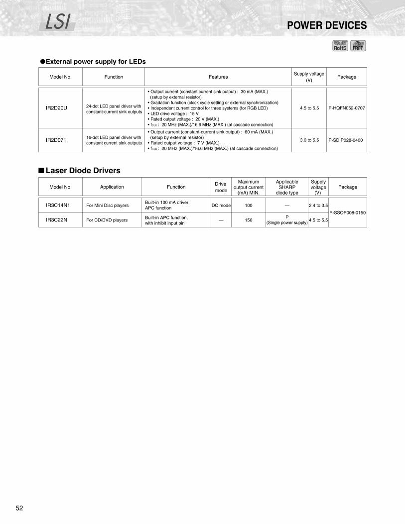
LSI
52
POWER DEVICES
External power supply for LEDs
Laser Diode Drivers
P-SDIP028-0400
Model No. Package
P-HQFN052-0707IR2D20U
IR2D071
Function FeaturesSupply voltage
(V)
4.5 to 5.5
3.0 to 5.5
24-dot LED panel driver with constant-current sink outputs
16-dot LED panel driver with constant current sink outputs
• Output current (constant current sink output) : 30 mA (MAX.) (setup by external resistor)• Gradation function (clock cycle setting or external synchronization)• Independent current control for three systems (for RGB LED)• LED drive voltage : 15 V• Rated output voltage : 20 V (MAX.)• fCLK : 20 MHz (MAX.)/16.6 MHz (MAX.) (at cascade connection)
• Output current (constant-current sink output) : 60 mA (MAX.) (setup by external resistor)• Rated output voltage : 7 V (MAX.)• fCLK : 20 MHz (MAX.)/16.6 MHz (MAX.) (at cascade connection)
P-SSOP008-0150
100
150
IR3C14N1
IR3C22N
Model No. Package
For Mini Disc players
For CD/DVD players
Built-in 100 mA driver, APC function
Built-in APC function, with inhibit input pin
Application FunctionDrive mode
Supplyvoltage
(V)
Maximumoutput current
(mA) MIN.
DC mode
—
—
P(Single power supply)
2.4 to 3.5
4.5 to 5.5
ApplicableSHARP
diode type
"

53
ANALOG ICs
New product
Under development
Video Interface ICs for TFT-LCDs
Power Amplifiers for Wireless LAN
4.5/12 or4.5/–7.5
4.5/12 or4.5/–7.5
3/12 or3/4.5/–7.5
Model No.Input signal LCD panelColor
decode
Serialdata
controlComposite
videoY/color
differenceOSD
(Digital)AnalogRGB
± powersource
+ powersource
Low voltagesource
PackageSupplyvoltage
(V) TYP.
Powerconsumption(mW) TYP.
Digitalinput
*1 For digital signal input panels *2 Built-in timing generator *3 Two inputs *4 Digital RGB input is also available. *5 At analog input for RGB
NTSC/PAL(automatic
identification)
NTSC/PAL(automatic
identification)
(Common terminal)
(Common terminal)
(Common terminal)
(Built-in)
P-QFP048-0707
P-QFP048-1010/P-QFP048-0707
P-QFP048-0707
P-QFP048-1010
P-QFP072-1010
P-QFP048-1010
P-LQFP100-1414
P-TQFP100-1414
130
140
190
160
88
106/88*5
92
70/57*5
95/80*5
120
330
250
197
257
300
5/7.5
3/12
3/6.5
3/5
3/5/13
3/7
5/13
3.3/5/7.5
3.3/5/13
3.3/5
NTSC/PAL
–
NTSC/PAL
NTSC/PAL
–
–
–
–
–
NTSC/PAL
NTSC/PAL
NTSC/PAL
NTSC/PAL
NTSC/PAL/SECAM
*3
*3
*3
*3
*4
IR3Y18A1
IR3Y26A2/A6
IR3Y29A1/B1
IR3Y31M1
IR3Y34M1
IR3Y37A1
RB5P0010M2
RB5P0020M2
RB5P0050M2
RB5P0060M2
RB5P006AM2
RB5P0070M*1
RB5P0090M
LRS5751*2
LRS5752*2
IR3Y63M
Supplycurrent
(mA) TYP.Model No. PackageApplication
Operating frequency
(GHz)
Supply voltage
(V) TYP.
Gain(dB) TYP.
Detectionfunction
Matchingcircuit
Output power(dBm) TYP.
* Can be used as a power amp for PHS and DECT (1.9 GHz band), or as a driver amp for FWA (1.9 to 2.6 GHz band).
18 (at EVM 3%)
18 (at EVM 2%)
18 (at EVM 3%)
18 (at EVM 3%)
18 (at EVM 3%)
16 (at EVM 2%)
18 (at EVM 3%)
18 (at EVM 2%)
2.4 to 2.5
4.9 to 5.9
2.4 to 2.5
4.9 to 5.9
2.4 to 2.5
4.9 to 5.9
For 5 GHz wireless LAN(IEEE 802.11a)
For 2.4 GHz wireless LAN (IEEE 802.11b/g)
For 2.4 GHz wireless LAN(IEEE 802.11b/g)
For 5 GHz wireless LAN(IEEE 802.11a)
For 2.4 GHz wireless LAN (IEEE 802.11b/g)
For 5 GHz wireless LAN(IEEE 802.11a)
For 2.4 GHz wireless LAN*(IEEE 802.11b/g)
Built-in(IN/OUT)
Built-in(IN/OUT)
Built-in(IN/OUT)
Built-in(IN/OUT)
Built-in(IN/OUT)
P-HQFN024-0404
P-HQFN016-0303
P-HQFN024-0404
P-HQFN010-0202A
P-HQFN024-0404
P-HQFN010-0202A
–
–
–
–
30
25
29
30
30
28
30
25
31
105
140
130
160
105
75
120
140
150
3.3
IRM046U7
IRM065U7
IRM047U7
IRM060U7
IRM063U7
IRM048U7
IRM053U7
Pow
er D
evic
es/
Anal
og IC
s
"
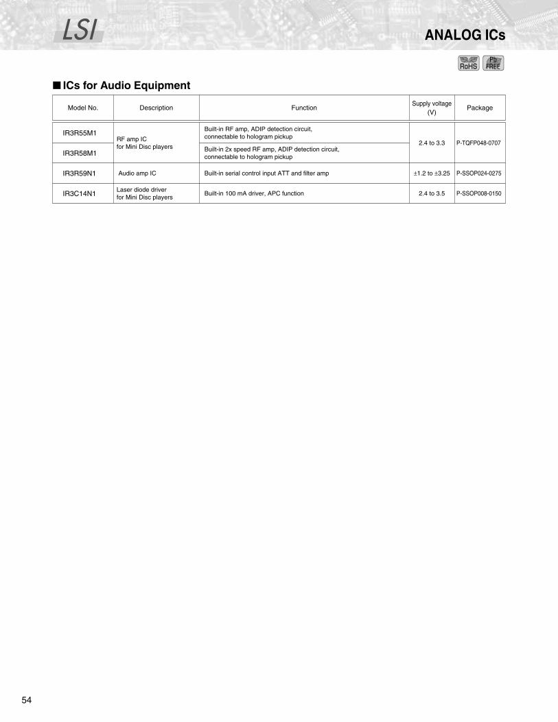
LSI
54
ANALOG ICs
ICs for Audio Equipment
P-TQFP048-0707
P-SSOP024-0275
P-SSOP008-0150
IR3R55M1
IR3R58M1
IR3R59N1
IR3C14N1
Model No. Package
Audio amp IC Built-in serial control input ATT and filter amp
Built-in 100 mA driver, APC function
2.4 to 3.3
±1.2 to ±3.25
2.4 to 3.5
Description FunctionSupply voltage
(V)
Built-in RF amp, ADIP detection circuit, connectable to hologram pickup
Built-in 2x speed RF amp, ADIP detection circuit, connectable to hologram pickup
RF amp IC for Mini Disc players
Laser diode driver for Mini Disc players
"!

LSI
55
Pack
ages
PACKAGES
CSP
CSP (Chip Size Package)
The FBGA (commonly known as CSP) has an area array terminal structure with solder balls on the bottom, to give it a near chip-size footprint. This high-density, compact and low-profile package technology will greatly help in the design of compact mobile equipment, such as mobile phones and digital cameras.
Wafer-level CSP
The wafer-level CSP (WL-CSP) is a kind of chip-size package which is manufactured by assembling directly onto the finished wafer.
FBGA (CSP)
Package height1.2 mm (MAX.)*
Gold wire Mold resin
Cu patternLead-free solder ball
Substrate
Diameter : 0.45 mm 0.4 mm 0.3 mm 0.24 mm
Bare chip
Terminal pitch : 0.8 mm 0.65 mm 0.5 mm 0.4 mm
Features
Crosssectionexample
Compact and lightweight Ability to create a near-chip size and lighter-weight package in comparison with conventional plastic packages.
High reliability Comparable high reliability with that of conventional plastic packages.
Mountability Conventional mounting system is available for CSP. SOP and QFP can be mounted together with CSP.
Terminal pitch
Maximum terminal counts
Nominal dimensions
0.8 mm
288 (16 mm x 16 mm)
0.65 mm
352 (16 mm x 16 mm)
6 mm x 6 mm to 16 mm x 16 mm
0.4 mm
264 (10 mm x 10 mm)
5 mm x 5 mm to 10 mm x 10 mm
0.5 mm
424 (14 mm x 14 mm)
* At 0.8 mm terminal pitch
Features
Crosssectionexample
Compact and thinner size It makes it possible to create an almost bare-chip-size and lighter-weight package.
Mountability The conventional CSP mounting system can be also used in that of wafer-level CSP, which facilitates chip mounting more than bare-chip mounting does. It can be mounted together with other existing packages and passive components. (The use of underfill is recommended to improve the reliability of assembly.)
Chip size*
Pad pitch
Maximum terminal counts
4 mm x 4 mm
49 (7 x 7) 81 (9 x 9)
* Rectangular chip form is also available.
0.5 mm 0.4 mm
3.5 mm x 3.5 mm
36 (6 x 6) 49 (7 x 7)
0.5 mm 0.4 mm
3 mm x 3 mm
25 (5 x 5) 36 (6 x 6)
0.5 mm 0.4 mm
2.5 mm x 2.5 mm
16 (4 x 4) 25 (5 x 5)
0.5 mm 0.4 mm
Lead-free solder ball
Passivation layer
Package height0.5 mm to 1 mm
Bare chipCu pattern
""
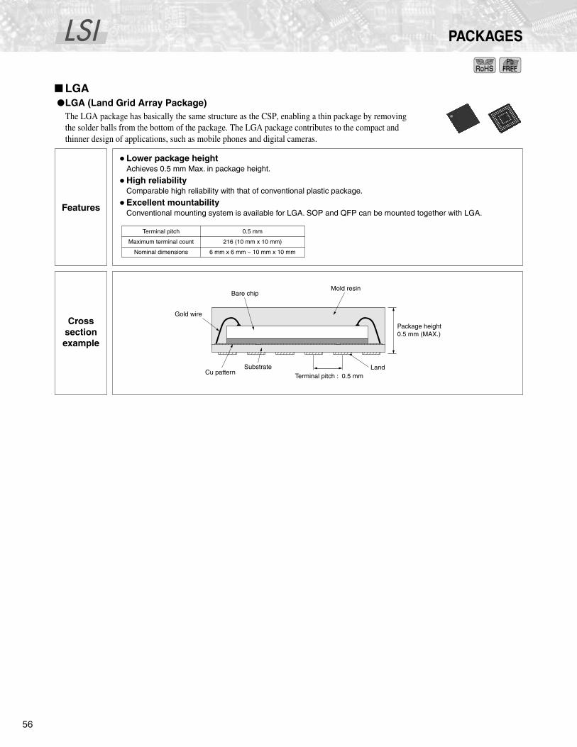
LSI
56
PACKAGES
LGA
LGA (Land Grid Array Package)
The LGA package has basically the same structure as the CSP, enabling a thin package by removing the solder balls from the bottom of the package. The LGA package contributes to the compact and thinner design of applications, such as mobile phones and digital cameras.
Features
Crosssectionexample
Lower package height Achieves 0.5 mm Max. in package height.
High reliability Comparable high reliability with that of conventional plastic package.
Excellent mountability Conventional mounting system is available for LGA. SOP and QFP can be mounted together with LGA.
Terminal pitch
Maximum terminal count
Nominal dimensions
0.5 mm
216 (10 mm x 10 mm)
6 mm x 6 mm ~ 10 mm x 10 mm
Land
Package height0.5 mm (MAX.)
Terminal pitch : 0.5 mmSubstrate
Cu pattern
Mold resinBare chip
Gold wire
"#

57
Pack
ages
PACKAGES
SiP (System in Package)
System in Package is an original SHARP high-density mounting technology that achieves high-density memory capacity and multiple functions by stacking multiple bare chips or multiple packages. This technology has two major streams. One method refers to a chip-stacked package technology that can achieve up to 5-chip mounting by stacking chips in a single package. The other method refers to a package stack technology with which it is possible to stack a package of over 5 chips, by stacking multiple packages in which 1 to 2 chips are stacked. The System in Package technology contributes to higher functionality of applications, such as mobile phones and digital cameras, as well as to reduction in size and weight.
Chip Stacked CSP
Chip Stacked TSOP/QFP*/VQFN/HQFN
Features
Crosssectionexample
(5-chip stacked CSP)
Wide variety of lineupIt is possible to provide a wide lineup of stacked CSPs, including 2-chip, 3-chip, 4-chip and 5-chip stacked CSPs, to respond to customer needs.
Compact and thinner sizeEncapsulating multiple bare chips into an existing plastic package contributes to decreasing the mounting area. In addition, SHARP's wafer thinning technology makes it possible to achieve 1.4 mm package height.
Multiple functionsMultiple bare chips of different sizes and functions, such as logic LSIs and memories, can be incorporated in a single package, making possible multiple functions.
Same-size chip stacking technologySHARP's stacking technology enables stacking of multiple same-size bare chips, contributing to higher memory density.
(4-chip stacked CSP)When using a SHARP four-chip stacked CSP, the mounting area and weight of a package can be decreased by half in comparison with using two 2-chip stacked CSPs, or a 3-chip stacked CSP and a conventional CSP.
Package height1.4 mm (MAX.)*1.6 mm (MAX.)*
Lead-free solder ball
Diameter : 0.45 mm0.30 mm
Terminal pitch : 0.8 mm0.5 mm
Cu pattern Substrate
Mold resinBare chipGold wire
* At 0.8 mm terminal pitch
Features
Crosssectionexample
* Including TQFP and LQFP.
Gold wire Bare chip Lead
Bare chip Mold resin
Package height1.2 mm (MAX.)
Decreased mounting areaBy encapsulating two identical or different types of bare chips into a single conventional plastic package, the mounting area of the package can be decreased.
Multiple functionsThanks to the incorporation of different sizes and functions of multiple bare chips, such as logic LSIs and memories, the functionality increases.
Higher memory densityWhen incorporating two identical memory bare chips into a single package, memory density doubles on the same mounting area.
(TSOP, TQFP)
(VQFN) Gold wire
Package height1.0 mm (MAX.)
Mold resin (HQFN) Gold wire
Package height1.0 mm (MAX.)
Mold resin
"
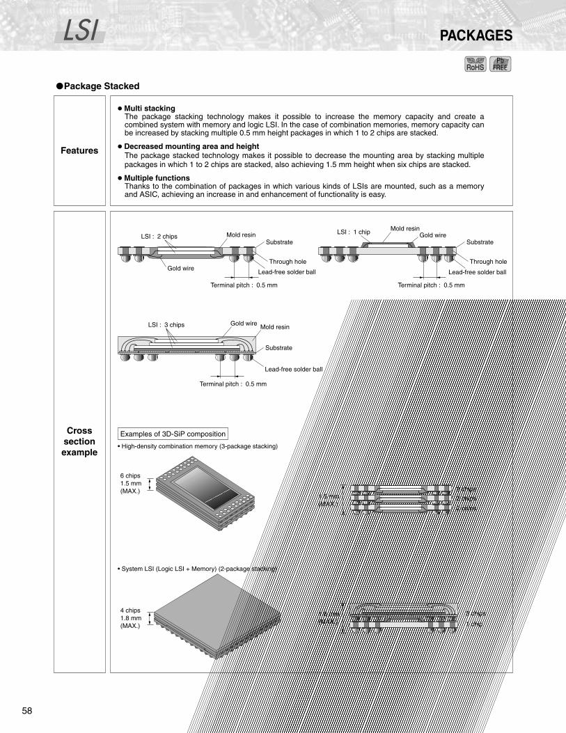
LSI
58
PACKAGES
Package Stacked
3 chips
1 chip
1.8 mm(MAX.)
LSI : 3 chips Gold wire Mold resin
Substrate
Lead-free solder ball
Terminal pitch : 0.5 mm
Features
Multi stackingThe package stacking technology makes it possible to increase the memory capacity and create a combined system with memory and logic LSI. In the case of combination memories, memory capacity can be increased by stacking multiple 0.5 mm height packages in which 1 to 2 chips are stacked.
Decreased mounting area and heightThe package stacked technology makes it possible to decrease the mounting area by stacking multiple packages in which 1 to 2 chips are stacked, also achieving 1.5 mm height when six chips are stacked.
Multiple functionsThanks to the combination of packages in which various kinds of LSIs are mounted, such as a memory and ASIC, achieving an increase in and enhancement of functionality is easy.
Crosssectionexample
Examples of 3D-SiP composition
6 chips1.5 mm(MAX.)
• High-density combination memory (3-package stacking)
1.5 mm(MAX.)
2 chips
2 chips
2 chips
• System LSI (Logic LSI + Memory) (2-package stacking)
4 chips1.8 mm(MAX.)
Gold wire
Mold resinSubstrate
Through hole
Lead-free solder ball
Terminal pitch : 0.5 mm
LSI : 2 chipsMold resin
Gold wireLSI : 1 chip
Substrate
Through hole
Lead-free solder ball
Terminal pitch : 0.5 mm
"

59
Pack
ages
PACKAGES
SOF
SOF (System On Film)
SOF is a highly flexible thin film package, created from SHARP’s TCP technologies. It can be easily bent, and contributes to thin and compact design of products.Peripheral circuit components can also be mounted.
Features
Crosssectionexample
Filmspecifications
Other components Bare chips and peripheral circuit components can be mounted on the film.
Highly flexible and thin film package By using highly flexible and thin film, SOF contributes to creating thin and compact products. It can also achieve finer terminal pitches and multiple outputs easily, and pattern layout on a film under the chip makes it possible to improve the flexibility of the pattern layout. Multiple chip mounting Plural bare chip mounting and incorporation of peripheral components contribute to the higher functionality of products.
Film width : W1
Maximum pattern layout area : W2
Maximum device pitch : L
Copper foil thickness
Copper foil type
Copper foil plating
Minimum pattern pitch
Sprocket hole : A
Sprocket hole : B
35 mm super wide
28.6 mm
48 mm super wide
41.6 mm
15 sprockets
8 µm
Rolled or electrolytic
Tin (Sn)
0.029 mm
1.981 mm (wide) /1.42 mm (super wide)
1.981 mm (wide) /1.42 mm (super wide)
70 mm wide
59.0 mm
Under fill material
Cu pattern
Solder resist
Gold bump
Bare chip
38 µm
B
A
L
W1 W2
Sprocket hole pitch
Max
imum
pat
tern
layo
ut a
rea
4.75 mm
Thickness 0.6 mm (MIN.)1.0 mm (TYP.)
In addition to the SOF described above, a conventional TCP (Tape Carrier Package) is also available.
"

LSI
60
PACKAGES
Under development
Package Lineup
Surface-mount TypePackage
typeAppearance
(Package material)Package code No. of terminals Terminal pitch
mmNominal dimensions
mm
Package width & lengthx (seated height [MAX.])
mm
(Plastic)
* Figures in brackets indicate available terminal counts.
FBGA(CSP)
LFBGA048-0606
TFBGA048-0608
TFBGA048-0808
TFBGA056-0808
TFBGA060-0811
TFBGA064-0811
TFBGA072-0811
LFBGA072-0811
TFBGA081-0808
LFBGA085-0811
LFBGA087-0811
LFBGA088-0811
LFBGA088-0912
LFBGA090-0811
TFBGA096-1010
LFBGA107-0912
TFBGA111-1010
TFBGA112-1010
LFBGA115-0914
LFBGA116-1010
LFBGA130-1013
TFBGA144-1111
TFBGA160-1212
LFBGA168-1212
TFBGA180-1212
TFBGA184-1212
TFBGA240-1414
LFBGA280-1616
LFBGA352-1616
TFBGA064-0606
LFBGA144-0909
LFBGA160-1010
TFBGA180-1313
LFBGA192-1010
LFBGA208-1212
LFBGA224-1313
TFBGA260-1313
6 x 6
6 x 8
8 x 8
8 x 11
8 x 8
8 x 11
9 x 12
8 x 11
10 x 10
9 x 12
10 x 10
9 x 14
10 x 10
10 x 13
11 x 11
12 x 12
14 x 14
16 x 16
6 x 6
9 x 9
10 x 10
13 x 13
10 x 10
12 x 12
13 x 13
6.0 x 6.0 x (1.4)
6.0 x 8.0 x (1.2)
8.0 x 8.0 x (1.2)
8.0 x 11.0 x (1.2)
8.0 x 11.0 x (1.4) /
8.0 x 8.0 x (1.2)
8.0 x 11.0 x (1.4) /
9.0 x 12.0 x (1.4) /
8.0 x 11.0 x (1.4) /
10.0 x 10.0 x (1.2)
9.0 x 12.0 x (1.4) /
10.0 x 10.0 x (1.2)
9.0 x 14.0 x (1.4) /
10.0 x 10.0 x (1.4) /
10.0 x 13.0 x (1.4) /
11.0 x 11.0 x (1.2)
12.0 x 12.0 x (1.2)
12.0 x 12.0 x (1.4) /
12.0 x 12.0 x (1.2)
14.0 x 14.0 x (1.2)
16.0 x 16.0 x (1.5)
6.0 x 6.0 x (1.2)
9.0 x 9.0 x (1.4)
10.0 x 10.0 x (1.4) /
13.0 x 13.0 x (1.2)
10.0 x 10.0 x (1.4) /
12.0 x 12.0 x (1.4) /
13.0 x 13.0 x (1.4) /
13.0 x 13.0 x (1.2)
48
56
60 (48)*
64
72 (64)*
81
85
87
88
90
96
107
111
112
115
116
130
144
160
168
180
184
240
280
352
64
140
160
180
192
208
224
260
0.8
0.65
(1.6)
(1.6)
(1.6)
(1.6)
(1.6)
(1.6)
(1.6)
(1.6)
(1.6)
(1.6)
(1.6)
(1.6)
(1.6)
#

61
Pack
ages
PACKAGES
Under development
Surface-mount Type (cont’d)Package
typeAppearance
(Package material)Package code No. of terminals Terminal pitch
mmNominal dimensions
mm
Package width & lengthx (seated height [MAX.])
mm
LFBGA064-0606
TFBGA068-0606
VFBGA081-0606
TFBGA084-0606
VFBGA100-0606
VFBGA100-0707
TFBGA100-0707
VFBGA108-0707
TFBGA108-0707
VFBGA120-0707
TFBGA120-0707
VFBGA144-0808
LFBGA144-0808
LFBGA144-0811
TFBGA152-0808
VFBGA171-0811
LFBGA171-0811
VFBGA176-0909
TFBGA176-0909
TFBGA180-0909
VFBGA188-1111
64
68
81
84
100
108
120
144
152
171
176
180
188
208
245
424
144
121
168
204
FBGA(CSP)
(Plastic)
6 x 6
7 x 7
8 x 8
8 x 11
8 x 8
8 x 11
9 x 9
11 x 11
6.0 x 6.0 x (1.1)
6.0 x 6.0 x (0.9)
6.0 x 6.0 x (1.1)
6.0 x 6.0 x (0.9)
7.0 x 7.0 x (0.9)
7.0 x 7.0 x (1.1)
7.0 x 7.0 x (0.9)
7.0 x 7.0 x (1.1)
7.0 x 7.0 x (0.9)
7.0 x 7.0 x (1.1)
8.0 x 8.0 x (0.9)
8.0 x 8.0 x (1.3) /
8.0 x 11.0 x (1.3)
8.0 x 8.0 x (1.1)
8.0 x 11.0 x (0.9)
8.0 x 11.0 x (1.3) /
9.0 x 9.0 x (0.9)
9.0 x 9.0 x (1.1)
11.0 x 11.0 x (0.9)
0.5
TFBGA188-0909
VFBGA208-1010
TFBGA208-1010
TFBGA245-1010
LFBGA245-1010
FBGA424-1414
WFBGA144-0606
WFBGA121-0606
TFBGA168-0707
TFBGA204-0808
9 x 9
10 x 10
14 x 14
6 x 6
7 x 7
8 x 8
9.0 x 9.0 x (1.1)
10.0 x 10.0 x (0.9)
10.0 x 10.0 x (1.1)
10.0 x 10.0 x (1.3)
14.0 x 14.0 x (1.8)
6.0 x 6.0 x (0.75)
6.0 x 6.0 x (0.8)
7.0 x 7.0 x (1.0)
8.0 x 8.0 x (1.0)
0.4
(1.5)
(1.5)
#
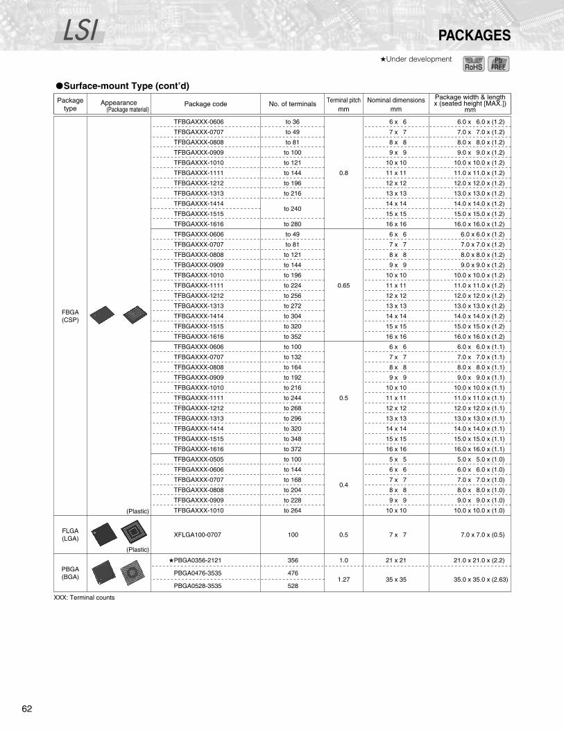
LSI
62
PACKAGES
Under development
Surface-mount Type (cont’d)Package
typeAppearance
(Package material)Package code No. of terminals Terminal pitch
mmNominal dimensions
mm
Package width & lengthx (seated height [MAX.])
mm
XXX: Terminal counts
TFBGAXXX-0606
TFBGAXXX-0707
TFBGAXXX-0808
TFBGAXXX-0909
TFBGAXXX-1010
TFBGAXXX-1111
TFBGAXXX-1212
TFBGAXXX-1313
TFBGAXXX-1414
TFBGAXXX-1515
TFBGAXXX-1616
TFBGAXXX-0606
TFBGAXXX-0707
TFBGAXXX-0808
TFBGAXXX-0909
TFBGAXXX-1010
TFBGAXXX-1111
TFBGAXXX-1212
TFBGAXXX-1313
TFBGAXXX-1414
TFBGAXXX-1515
TFBGAXXX-1616
TFBGAXXX-0606
TFBGAXXX-0707
TFBGAXXX-0808
TFBGAXXX-0909
TFBGAXXX-1010
TFBGAXXX-1111
TFBGAXXX-1212
TFBGAXXX-1313
TFBGAXXX-1414
TFBGAXXX-1515
TFBGAXXX-1616
TFBGAXXX-0505
TFBGAXXX-0606
TFBGAXXX-0707
TFBGAXXX-0808
TFBGAXXX-0909
TFBGAXXX-1010
to 36
to 49
to 81
to 100
to 121
to 144
to 196
to 216
to 240
to 280
to 49
to 81
to 121
to 144
to 196
to 224
to 256
to 272
to 304
to 320
to 352
to 100
to 132
to 164
to 192
to 216
to 244
to 268
to 296
to 320
to 348
to 372
to 100
to 144
to 168
to 204
to 228
to 264
FBGA(CSP)
PBGA(BGA)
FLGA(LGA)
(Plastic)
(Plastic)
6 x 6
7 x 7
8 x 8
9 x 9
10 x 10
11 x 11
12 x 12
13 x 13
14 x 14
15 x 15
16 x 16
6 x 6
7 x 7
8 x 8
9 x 9
10 x 10
11 x 11
12 x 12
13 x 13
14 x 14
15 x 15
16 x 16
6 x 6
7 x 7
8 x 8
9 x 9
10 x 10
11 x 11
12 x 12
13 x 13
14 x 14
15 x 15
16 x 16
5 x 5
6 x 6
7 x 7
8 x 8
9 x 9
10 x 10
6.0 x 6.0 x (1.2)
7.0 x 7.0 x (1.2)
8.0 x 8.0 x (1.2)
9.0 x 9.0 x (1.2)
10.0 x 10.0 x (1.2)
11.0 x 11.0 x (1.2)
12.0 x 12.0 x (1.2)
13.0 x 13.0 x (1.2)
14.0 x 14.0 x (1.2)
15.0 x 15.0 x (1.2)
16.0 x 16.0 x (1.2)
6.0 x 6.0 x (1.2)
7.0 x 7.0 x (1.2)
8.0 x 8.0 x (1.2)
9.0 x 9.0 x (1.2)
10.0 x 10.0 x (1.2)
11.0 x 11.0 x (1.2)
12.0 x 12.0 x (1.2)
13.0 x 13.0 x (1.2)
14.0 x 14.0 x (1.2)
15.0 x 15.0 x (1.2)
16.0 x 16.0 x (1.2)
6.0 x 6.0 x (1.1)
7.0 x 7.0 x (1.1)
8.0 x 8.0 x (1.1)
9.0 x 9.0 x (1.1)
10.0 x 10.0 x (1.1)
11.0 x 11.0 x (1.1)
12.0 x 12.0 x (1.1)
13.0 x 13.0 x (1.1)
14.0 x 14.0 x (1.1)
15.0 x 15.0 x (1.1)
16.0 x 16.0 x (1.1)
5.0 x 5.0 x (1.0)
6.0 x 6.0 x (1.0)
7.0 x 7.0 x (1.0)
8.0 x 8.0 x (1.0)
9.0 x 9.0 x (1.0)
10.0 x 10.0 x (1.0)
0.8
0.65
0.5
0.4
XFLGA100-0707 100 7 x 7 7.0 x 7.0 x (0.5)0.5
PBGA0356-2121
PBGA0476-3535
PBGA0528-3535
356
476
528
21 x 21
35 x 35
21.0 x 21.0 x (2.2)
35.0 x 35.0 x (2.63)
1.0
1.27
#
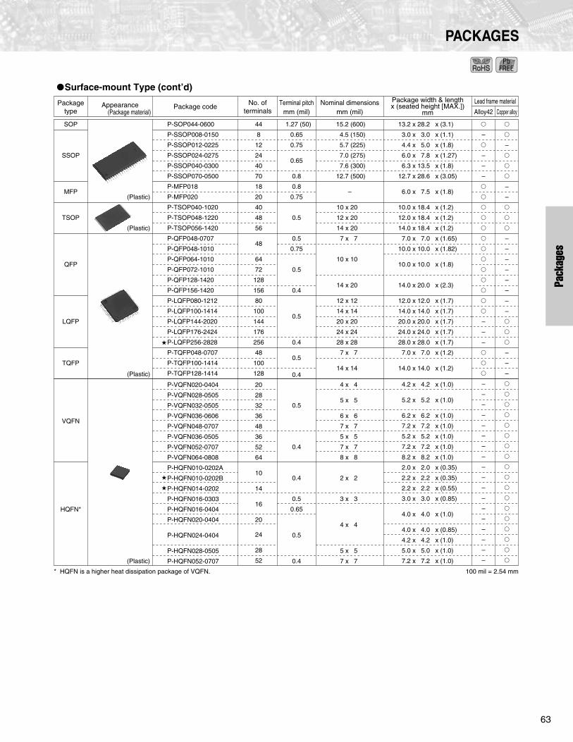
63
Pack
ages
PACKAGES
Surface-mount Type (cont’d)
Packagetype
Appearance(Package material)
Package code No. ofterminals
Terminal pitchmm (mil)
Nominal dimensionsmm (mil)
Package width & lengthx (seated height [MAX.])
mm
Lead frame material
Copper alloyAlloy42
(Plastic)
(Plastic)
(Plastic)
(Plastic)
100 mil = 2.54 mm* HQFN is a higher heat dissipation package of VQFN.
–
–
–
–
–
–
–
–
–
–
–
–
–
–
–
–
–
–
–
–
–
–
–
–
–
–
–
–
–
–
–
–
–
–
–
–
–
–
–
13.2 x 28.2 x (3.1)
3.0 x 3.0 x (1.1)
4.4 x 5.0 x (1.8)
6.0 x 7.8 x (1.27)
6.3 x 13.5 x (1.8)
12.7 x 28.6 x (3.05)
6.0 x 7.5 x (1.8)
10.0 x 18.4 x (1.2)
12.0 x 18.4 x (1.2)
14.0 x 18.4 x (1.2)
7.0 x 7.0 x (1.65)
10.0 x 10.0 x (1.82)
10.0 x 10.0 x (1.8)
14.0 x 20.0 x (2.3)
12.0 x 12.0 x (1.7)
14.0 x 14.0 x (1.7)
20.0 x 20.0 x (1.7)
24.0 x 24.0 x (1.7)
28.0 x 28.0 x (1.7)
7.0 x 7.0 x (1.2)
14.0 x 14.0 x (1.2)
P-SOP044-0600
P-SSOP008-0150
P-SSOP012-0225
P-SSOP024-0275
P-SSOP040-0300
P-SSOP070-0500
P-MFP018
P-MFP020
P-TSOP040-1020
P-TSOP048-1220
P-TSOP056-1420
P-QFP048-0707
P-QFP048-1010
P-QFP064-1010
P-QFP072-1010
P-QFP128-1420
P-QFP156-1420
P-LQFP080-1212
P-LQFP100-1414
P-LQFP144-2020
P-LQFP176-2424
P-LQFP256-2828
P-TQFP048-0707
P-TQFP100-1414
P-TQFP128-1414
15.2 (600)
4.5 (150)
5.7 (225)
7.0 (275)
7.6 (300)
12.7 (500)
–
10 x 20
12 x 20
14 x 20
7 x 7
10 x 10
14 x 20
12 x 12
14 x 14
20 x 20
24 x 24
28 x 28
7 x 7
14 x 14
44
8
12
24
40
70
18
20
40
48
56
48
64
72
128
156
80
100
144
176
256
48
100
128
SOP
SSOP
MFP
TSOP
QFP
LQFP
TQFP
1.27 (50)
0.65
0.75
0.65
0.8
0.8
0.75
0.5
0.5
0.75
0.5
0.4
0.5
0.4
0.5
0.4
4.2 x 4.2 x (1.0)
5.2 x 5.2 x (1.0)
6.2 x 6.2 x (1.0)
7.2 x 7.2 x (1.0)
5.2 x 5.2 x (1.0)
7.2 x 7.2 x (1.0)
8.2 x 8.2 x (1.0)
2.0 x 2.0 x (0.35)
2.2 x 2.2 x (0.35)
2.2 x 2.2 x (0.55)
3.0 x 3.0 x (0.85)
4.0 x 4.0 x (1.0)
4.0 x 4.0 x (0.85)
4.2 x 4.2 x (1.0)
5.0 x 5.0 x (1.0)
7.2 x 7.2 x (1.0)
P-VQFN020-0404
P-VQFN028-0505
P-VQFN032-0505
P-VQFN036-0606
P-VQFN048-0707
P-VQFN036-0505
P-VQFN052-0707
P-VQFN064-0808
P-HQFN010-0202A
P-HQFN010-0202B
P-HQFN014-0202
P-HQFN016-0303
P-HQFN016-0404
P-HQFN020-0404
P-HQFN024-0404
P-HQFN028-0505
P-HQFN052-0707
4 x 4
5 x 5
6 x 6
7 x 7
5 x 5
7 x 7
8 x 8
2 x 2
3 x 3
4 x 4
5 x 5
7 x 7
20
28
32
36
48
36
52
64
10
14
16
20
24
28
52
VQFN
HQFN*
0.5
0.4
0.4
0.5
0.65
0.5
0.4
#

LSI
64
PACKAGES
For CCDs
Packagetype
Appearance(Package material)
(Plastic)
(Ceramic)
(Ceramic)
(Plastic)
Package codeNo. of
terminalsTerminal pitch
mmNominal dimensions
mm (mil)
Package width & lengthx (seated height)
mm
P-DIP014-0400A
P-DIP016-0500C
P-DIP020-0400
N-DIP016-0450
N-DIP016-0500C
P-SOP028-0400
P-SOP032-0525
N-LCC028-S450A
N-LCC032-R543
14
16
20
16
28
32
28
32
DIP
SOP
LCC
1.27
1.78
1.00
1.27
1.78
0.69
0.78
0.80
0.80
10.16 (400)
12.7 (500)
10.16 (400)
11.43 (450)
12.7 (500)
10.16 (400)
13.3 (525)
11.5
13.8
10.0 x 10.0
12.4 x 14.0
10.0 x 10.0
11.4 x 12.2
12.4 x 14.0
10.0 x 10.0 x (3.5)
12.0 x 13.8 x (3.9)
11.5 x 11.5 x (1.62)
12.9 x 13.8 x (1.35)
100 mil = 2.54 mm
FBGA : fine-pitch ball grid array package
FLGA : fine-pitch land grid array package
PBGA : plastic ball grid array package
SOP : small outline package
SSOP : shrink small outline package
MFP : mini flat package
TSOP : thin small outline package
QFP : quad flat package
LQFP : low profile quad flat package
TQFP : thin quad flat package
VQFN : very thin quad flat non-leaded package
HQFN : heat sink quad flat non-leaded package
DIP : dual inline package
LCC : leadless chip carrier
Nominal dimensions
FBGA (CSP)FLGA (LGA)PBGA (BGA)
SOPSSOPMFP
VQFNHQFN
QFPLQFPTQFP
TSOP
DIP LCC
#!

65
Pack
ages
PACKAGES
Lead-inserting Type Packages [For regulators: PQ series]
Surface-mount Type Packages [For regulators/LED drivers: PQ series]
Package type Appearance No.ofterminals
Terminal pitchmm
Outline dimensions(Width x Thickness x Height) mm
Lead framematerial(Package material)
(Plastic)
(Plastic)
(Plastic)
(Plastic)
(Plastic)
(Plastic)
(Plastic)
*1 The figure in parentheses indicates reference value.*2 Including lead length
TO-220(Heat sink exposure)[Lead forming type]
TO-220(Full mold)[Lead forming type]
TO-220[Lead forming type]
TO-220[Lead forming type]
TO-220(Full mold)
Cu
Cu
Cu
Cu
Cu
Cu
Cu
A
B
C
D
E
5
4
4
5
5
5
3
(1.7)*1
2.54
2.54
(1.7)*1
(1.7)*1
(1.7)*1
2.5
10.2 (MAX.) x 3.5 x 25.2*2
10.2 (MAX.) x 4.5 x 29.1*2
10.2 (MAX.) x 4.5 x 29.1*2
10.2 (MAX.) x 4.5 x 24.6*2
10.2 (MAX.) x 4.5 x 24.6*2
10.2 (MAX.) x 4.5 x 24.6*2
TO-220
TO-92 5.2 (MAX.) x 4.2 (MAX.) x 18.2 (MAX.)*2
(Plastic)
(Plastic)
(Plastic)
(Plastic)
*1 The figure in parentheses indicates reference value.*2 Including lead length
Package type No.ofterminals
Terminal pitchmm
Outline dimensions(Width x Height x Thickness) mm
Lead framematerial
Cu
Cu
Cu
Cu
5(Heat sink
not included)
5(Heat sink
not included)
5(Heat sink included)
Appearance(Package material)
8
(1.7)*1
(1.27)*1
(1.27)*1
1.27
TO-263
SC-63
SC-63
SOP-8
F
G
10.6 (MAX). x 13.7 (MAX.)*2 x 3.5
6.6 (MAX.) x 9.7 (MAX.)*2 x 2.3
6.6(MAX.) x 9.7 (MAX.)*2 x 2.1
5 x 6.2*2 x 1.55*2
#"
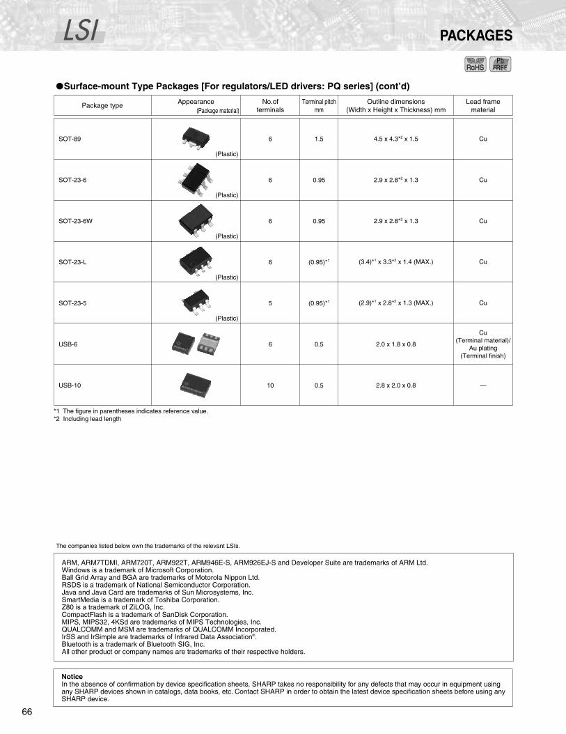
LSI
66
PACKAGES
Surface-mount Type Packages [For regulators/LED drivers: PQ series] (cont’d)
The companies listed below own the trademarks of the relevant LSIs.
Notice
In the absence of confirmation by device specification sheets, SHARP takes no responsibility for any defects that may occur in equipment using any SHARP devices shown in catalogs, data books, etc. Contact SHARP in order to obtain the latest device specification sheets before using any SHARP device.
(Plastic)
(Plastic)
(Plastic)
(Plastic)
(Plastic)
*1 The figure in parentheses indicates reference value.*2 Including lead length
Package type No.ofterminals
Terminal pitchmm
Outline dimensions(Width x Height x Thickness) mm
Lead framematerial
Cu
Cu
Cu
Cu(Terminal material)/
Au plating(Terminal finish)
Cu
Cu
Appearance(Package material)
6
6
6
6
5
6
10
1.5
0.95
0.95
(0.95)*1
(0.95)*1
0.5
0.5
SOT-89
SOT-23-6
SOT-23-6W
SOT-23-L
SOT-23-5
USB-6
USB-10
4.5 x 4.3*2 x 1.5
2.9 x 2.8*2 x 1.3
2.9 x 2.8*2 x 1.3
2.0 x 1.8 x 0.8
2.8 x 2.0 x 0.8
(3.4)*1 x 3.3*2 x 1.4 (MAX.)
(2.9)*1 x 2.8*2 x 1.3 (MAX.)
—
ARM, ARM7TDMI, ARM720T, ARM922T, ARM946E-S, ARM926EJ-S and Developer Suite are trademarks of ARM Ltd.Windows is a trademark of Microsoft Corporation.Ball Grid Array and BGA are trademarks of Motorola Nippon Ltd.RSDS is a trademark of National Semiconductor Corporation.Java and Java Card are trademarks of Sun Microsystems, Inc.SmartMedia is a trademark of Toshiba Corporation.Z80 is a trademark of ZiLOG, Inc.CompactFlash is a trademark of SanDisk Corporation.MIPS, MIPS32, 4KSd are trademarks of MIPS Technologies, Inc.QUALCOMM and MSM are trademarks of QUALCOMM Incorporated.IrSS and IrSimple are trademarks of Infrared Data Association®.Bluetooth is a trademark of Bluetooth SIG, Inc.All other product or company names are trademarks of their respective holders.
##

OPTO
67
Opto
elec
tron
ics
PHOTOCOUPLER INDEX TREE
Photocoupler Lineup
<Phototransistor output type>
<OPIC output type>
The model marked with
may not be available in the near future. Contact with SHARP for details before use.
Package type Output type Features Model No. (series) Page
4-pin SOP Compact, SMT type Single phototransistor
General purpose, High collector-emitter voltage, etc. PC35x series/PC451J00000F 68
Low input current PC367NJ0000F 68
AC input response PC354NJ0000F 68
High sensitivity, High collector-emitter voltage
Low input current PC364NJ0000F 68
Darlington phototransistor PC355NJ0000F 68
Low input current PC365NJ0000F 68
Compact, Half pitch (lead space), SMT type Single phototransistor
General purpose, High collector-emitter voltage, etc. PC3Hx series 69
Low input current PC3H71xNIP0F 69
High collector-emitter voltage PC4H510NIP0F 69
AC input response PC3H3J00000F/PC3H4J00000F 69
Low input current PC3H41xNIP0F 69
4-channel output PC3Q62J0000F
/PC3Q67QJ000F
69
Low input current PC3Q71xNIP0F
69
AC input response PC3Q63J0000F
/PC3Q64QJ000F
69
Low input current PC3Q41xNIP0F
69
Darlington phototransistor General purpose PC3H5J00000F 69
Low input current PC3H510NIP0F 69
High collector-emitter voltage PC4H520NIP0F
69
4-channel output PC3Q65J0000F
69
Low input current PC3Q510NIP0F
69
DIP type (4/16-pin) Single phototransistorApproved by safety standards other than UL
Isolation thickness: 0.4 mm or more Creepage distance: 6.4 mm or more PC123J00000F series 70
General purpose, High collector-emitter voltage, etc.
Low input current PC1231xNSZ0F 70
PC817XJ0000F/PC847XJ0000F/PC851XJ0000F 70
Low input current PC817xxNSZ0F 70
AC input response PC814XJ0000F/PC844XJ0000F 70
Low input current PC8141xNSZ0F 70
Built-in SBD/High response speed PC81100NSZ0F 70
Darlington phototransistorGeneral purpose, High collector-emitter voltage
PC815XJ0000F/PC845XJ0000F/PC852XJ0000F/PC853XJ0000F 70
Low input current PC81510NSZ0F 70
DIP type (6-pin) Single phototransistorGeneral purpose, High collector-emitter voltage, etc. PC7xxV0NSZXF 71
Darlington phototransistorGeneral purpose, High collector-emitter voltage, etc. PC7x5V0NSZXF 71
Package type Output type Features Model No. (series) Page
Compact, SMT type Digital output General purpose, High response speed, 2ch, etc.
PC4xxJ00000F/PC456L0NIP0F/PC41xS0NIP0F/PC410L0NIP0F/PC411L0NIP0F/PC4D10SNIP0F 72
Analog/Digital output High CMR PC457S0NIP0F/PC457L0NIP0F 73
DIP type, SMT type Digital output General purpose, High response speed, etc.
PC9xxV0NSZXF/PC956L0NSZ0F/PC910L0NSZ0F/PC911L0NSZ0F/PC912L0NSZ0F
73
Built-in base amplifierFor inverter control/For inverter control, Built-in short-circuit protection circuit
PC928J00000F
/PC929J00000F
/PC942J00000F/PC92xL0NSZ0F series 74
Analog/Digital output High speed, High CMR, etc. PC957L0NSZ0F 74
#

OPTO
68
PHOTOCOUPLERS
Photocouplers
Phototransistor Output <Compact, SMT type>
*1 CMR: MIN.10 kV/µs*2 Please refer to Specification Sheets for model numbers approved by safety standards.
A VDE approved type is optionally available.
Out
put T
ype
Model No.Internal
connection diagram
Features
Approved by safety
standards*
2
Package
Absolute maximum ratings Electro-optical characteristics
Forward current
I
F
(mA)
Isolation voltage
(AC) Viso (rms)(kV)
Collector-emitter voltage
V
CEO
(V)
Current transfer ratio
Response time
CTR (%) MIN.
I
F
(mA)V
CE
(V)
tr (µs) TYP.
I
C
(mA)
R
L
(
Ω
)V
CE
(V)UL
Sin
gle
phot
otra
nsis
tor o
utpu
t
PC357NJ0000F General purpose
Mini-flat 4-pin
50 3.75 80 50 5 5 4 2 100 2
PC352NJ000F General purpose, high resistance to noise*
1
50 3.75 80 90 5 5 4 2 100 2
PC451J00000F High collector-emitter voltage
50 3.75 350 40 5 5 4 2 100 2
PC367NJ0000F Low input current, high CMR (MIN. 10kV/µs)
10 3.75 80 100 0.5 5 4 2 100 2
PC354NJ0000F AC input response
±50 3.75 80 20 ±1 5 4 2 100 2
PC364NJ0000FLow input current, high resistance to noise*
1
, AC input response
±10 3.75 70 50 ±0.5 5 4 2 100 2
Dar
lingt
on p
hoto
-tra
nsis
tor o
utpu
t
PC355NJ0000F High sensitivity
50 3.75 35 600 1 2 60 2 100 2
PC365NJ0000F High sensitivity, low input current
10 3.75 35 600 0.5 2 60 2 100 2
PC357NJ0000F(Mini-flat 4-pin)
*PC353TJ0000F only: Same shape, 5-pin
(Ta = 25°C): Approved, o: Under application
Notice
In the absence of confirmation by device specification sheets, SHARP takes no responsibility for any defects that may occur in equipment using any SHARP devices shown in catalogs, data books, etc. Except where specially indicated, models listed on this page comply with the RoHS Directive*. For details, please contact SHARP.*RoHS Directive: Prohibits use of lead, cadmium, hexavalent chromium, mercury and specific brominated flame retardants (PBBs and PBDEs), with certain exceptions.Contact SHARP in order to obtain the latest device specification sheets before using any SHARP device.
#
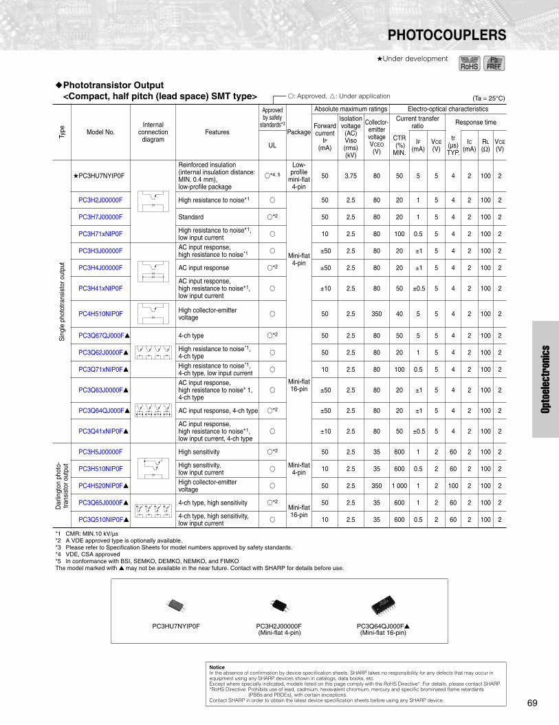
69
Opto
elec
tron
ics
PHOTOCOUPLERS
Under development
Phototransistor Output <Compact, half pitch (lead space) SMT type>
*1 CMR: MIN.10 kV/µs*2 A VDE approved type is optionally available.*3 Please refer to Specification Sheets for model numbers approved by safety standards.*4 VDE, CSA approved*5 In conformance with BSI, SEMKO, DEMKO, NEMKO, and FIMKOThe model marked with
may not be available in the near future. Contact with SHARP for details before use.
Type Model No.
Internal connection
diagramFeatures
Approved by safety
standards*
3
Package
Absolute maximum ratings Electro-optical characteristics
Forward current
I
F
(mA)
Isolation voltage
(AC) Viso (rms)(kV)
Collector-emitter voltage
V
CEO
(V)
Current transfer ratio Response time
CTR (%) MIN.
I
F
(mA)V
CE
(V)
tr (µs) TYP.
I
C
(mA)
R
L
(
Ω
)V
CE
(V)UL
Sin
gle
phot
otra
nsis
tor o
utpu
t
PC3HU7NYIP0F
Reinforced insulation (internal insulation distance: MIN. 0.4 mm), low-profile package
*
4, 5
Low-profile
mini-flat 4-pin
50 3.75 80 50 5 5 4 2 100 2
PC3H2J00000F High resistance to noise*
1
Mini-flat 4-pin
50 2.5 80 20 1 5 4 2 100 2
PC3H7J00000F Standard
*
2
50 2.5 80 20 1 5 4 2 100 2
PC3H71xNIP0F High resistance to noise*
1
, low input current
10 2.5 80 100 0.5 5 4 2 100 2
PC3H3J00000F AC input response, high resistance to noise
*1
±50 2.5 80 20 ±1 5 4 2 100 2
PC3H4J00000F AC input response
*
2
±50 2.5 80 20 ±1 5 4 2 100 2
PC3H41xNIP0FAC input response, high resistance to noise*
1
, low input current
±10 2.5 80 50 ±0.5 5 4 2 100 2
PC4H510NIP0F High collector-emitter voltage
50 2.5 350 40 5 5 4 2 100 2
PC3Q67QJ000F
4-ch type
*
2
Mini-flat 16-pin
50 2.5 80 50 5 5 4 2 100 2
PC3Q62J0000F
High resistance to noise
*1
,4-ch type
50 2.5 80 20 1 5 4 2 100 2
PC3Q71xNIP0F
High resistance to noise
*1
, 4-ch type, low input current
10 2.5 80 100 0.5 5 4 2 100 2
PC3Q63J0000F
AC input response, high resistance to noise* 1, 4-ch type
±50 2.5 80 20 ±1 5 4 2 100 2
PC3Q64QJ000F
AC input response, 4-ch type
*
2
±50 2.5 80 20 ±1 5 4 2 100 2
PC3Q41xNIP0F
AC input response, high resistance to noise*
1
, low input current, 4-ch type
±10 2.5 80 50 ±0.5 5 4 2 100 2
Dar
lingt
on p
hoto
-tra
nsis
tor o
utpu
t
PC3H5J00000F High sensitivity
*
2
Mini-flat 4-pin
50 2.5 35 600 1 2 60 2 100 2
PC3H510NIP0F High sensitivity, low input current
10 2.5 35 600 0.5 2 60 2 100 2
PC4H520NIP0F
High collector-emitter voltage
50 2.5 350 1 000 1 2 100 2 100 2
PC3Q65J0000F
4-ch type, high sensitivity
*
2
Mini-flat 16-pin
50 2.5 35 600 1 2 60 2 100 2
PC3Q510NIP0F
4-ch type, high sensitivity, low input current
10 2.5 35 600 0.5 2 60 2 100 2
PC3HU7NYIP0F PC3H2J00000F(Mini-flat 4-pin)
PC3Q64QJ000F
(Mini-flat 16-pin)
(Ta = 25°C): Approved, o: Under application
Notice
In the absence of confirmation by device specification sheets, SHARP takes no responsibility for any defects that may occur in equipment using any SHARP devices shown in catalogs, data books, etc. Except where specially indicated, models listed on this page comply with the RoHS Directive*. For details, please contact SHARP.*RoHS Directive: Prohibits use of lead, cadmium, hexavalent chromium, mercury and specific brominated flame retardants (PBBs and PBDEs), with certain exceptions.Contact SHARP in order to obtain the latest device specification sheets before using any SHARP device.
#

OPTO
70
PHOTOCOUPLERS
Phototransistor Output <DIP type (4/16-pin)>
*1 Wide lead spacing type (F type) is also available. Creepage distance PC123: 6.4 mm or more, PC123F: 8 mm or more*2 Optionally available.*3 BSI, SEMKO, DEMKO, NEMKO, FIMKO, CSA*4 CMR: 10 kV/µs MIN.*5 Lead forming type (I type) is also available for surface mounting.*6 Taped package of lead forming type for surface mounting is also available.*7
Wide lead spacing type (F type) is also available. Lead forming type (FI type) of F type is also available.Taped package is also available for I and FI type of lead forming type.
*8 Please refer to Specification Sheets for model numbers approved by safety standards.*9 Approved by UL as multi-channel type of PC817.
Out
put T
ype
Model No.Internal
connection diagram
Features
Approved by safety standards*
8
Package
Absolute maximum ratings Electro-optical characteristics
Forward current
I
F
(mA)
Isolation voltage
(AC) Viso (rms)
(kV)
Collector-emitter voltage
V
CEO
(V)
Current transfer ratio Response time
UL VDE*
2
Others*
3
CTR (%)
MIN.
I
F
(mA)
tr (µs) TYP.
R
L
(
Ω
)
Sin
gle
phot
otra
nsis
tor o
utpu
t
PC123J00000F*
1
High isolation voltage, long creepage distance
4-pinDIP
50 5.0 70 50 5 4 100
PC1231xNSZ0FHigh isolation voltage, long creepage distance, low input current, high resistance to noise
*4
– 10 5.0 70 50 0.5 4 100
PC817XJ0000F*
5,
*
6,
*
7
High isolation voltage
– 50 5.0 80 50 5 4 100
PC847XJ0000F*
5,
*
9
High isolation voltage (4-ch)
– 16-pinDIP 50 5.0 80 50 5 4 100
PC8171xNSZ0F High isolation voltage, low input current, high resistance to noise
*4
– –
4-pinDIP
10 5.0 70 100 0.5 4 100
PC851XJ0000F High isolation voltage, high collector-emitter voltage
– – 50 5.0 350 40 5 4 100
PC814XJ0000F*
5,
*
6
High isolation voltage, AC input response
– ±50 5.0 80 20 ±1 4 100
PC844XJ0000F High isolation voltage, AC input response (4-ch)
– 16-pinDIP ±50 5.0 80 20 ±1 4 100
PC8141xNSZ0FHigh isolation voltage, AC input response, low input current, high resistance to noise
*4
– –
4-pinDIP
±10 5.0 80 50 ±0.5 4 100
PC81100NSZ0FBuilt-in schottky barrier diode, toff: 35µs TYP. (In saturation, R
L
= 100k
Ω
)
– – 50 5.0 70 50 5ton: TYP.
9100
Dar
lingt
on p
hoto
trans
isto
r out
put
PC815XJ0000F High isolation voltage, high sensitivity
– – 4-pinDIP 50 5.0 35 600 1 60 100
PC845XJ0000F High isolation voltage, high sensitivity (4-ch)
– – 16-pinDIP 50 5.0 35 600 1 60 100
PC81510NSZ0F High isolation voltage, high sensitivity, low input current
– –
4-pinDIP
10 5.0 35 600 0.5 60 100
PC852XJ0000F*
5,
*
6
High isolation voltage, high collector-emitter voltage
– 50 5.0 350 1 000 1 100 100
PC853XJ0000F*
5,
*
6
High isolation voltage, high collector-emitter voltage
– 50 5.0 350 1 000 1 100 100
PC817XJ0000F(4-pin DIP)
PC847XJ0000F(16-pin DIP)
(Ta = 25°C): Approved, o: Under application
Schottky barrier diode
Notice
In the absence of confirmation by device specification sheets, SHARP takes no responsibility for any defects that may occur in equipment using any SHARP devices shown in catalogs, data books, etc. Except where specially indicated, models listed on this page comply with the RoHS Directive*. For details, please contact SHARP.*RoHS Directive: Prohibits use of lead, cadmium, hexavalent chromium, mercury and specific brominated flame retardants (PBBs and PBDEs), with certain exceptions.Contact SHARP in order to obtain the latest device specification sheets before using any SHARP device.
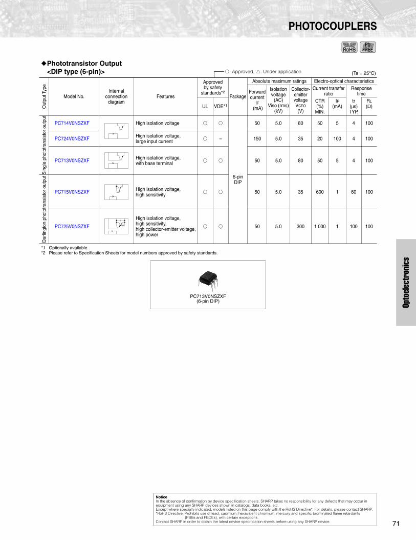
71
Opto
elec
tron
ics
PHOTOCOUPLERS
Phototransistor Output <DIP type (6-pin)>
*1 Optionally available.*2 Please refer to Specification Sheets for model numbers approved by safety standards.
Out
put T
ype
Model No.Internal
connection diagram
Features
Approved by safety
standards*
2
Package
Absolute maximum ratings Electro-optical characteristics
Forward current
I
F
(mA)
Isolation voltage
(AC) Viso (rms)
(kV)
Collector-emitter voltage
V
CEO
(V)
Current transfer ratio
Response time
UL VDE*
1
CTR (%)
MIN.
I
F
(mA)
tr (µs) TYP.
R
L
(
Ω
)
Sin
gle
phot
otra
nsis
tor o
utpu
t
PC714V0NSZXF High isolation voltage
6-pinDIP
50 5.0 80 50 5 4 100
PC724V0NSZXF High isolation voltage, large input current
– 150 5.0 35 20 100 4 100
PC713V0NSZXF High isolation voltage, with base terminal
50 5.0 80 50 5 4 100
Dar
lingt
on p
hoto
trans
isto
r out
put
PC715V0NSZXF High isolation voltage, high sensitivity
50 5.0 35 600 1 60 100
PC725V0NSZXF
High isolation voltage, high sensitivity, high collector-emitter voltage, high power
50 5.0 300 1 000 1 100 100
PC713V0NSZXF(6-pin DIP)
(Ta = 25°C): Approved, o: Under application
Notice
In the absence of confirmation by device specification sheets, SHARP takes no responsibility for any defects that may occur in equipment using any SHARP devices shown in catalogs, data books, etc. Except where specially indicated, models listed on this page comply with the RoHS Directive*. For details, please contact SHARP.*RoHS Directive: Prohibits use of lead, cadmium, hexavalent chromium, mercury and specific brominated flame retardants (PBBs and PBDEs), with certain exceptions.Contact SHARP in order to obtain the latest device specification sheets before using any SHARP device.

OPTO
72
PHOTOCOUPLERS
OPIC
∗
Output <Compact, SMT type> (1-1)
A: Rated voltage circuit*1 Each item is measured at Vcc=5V. (PC400, PC401)*2 Please refer to Specification Sheets for model numbers approved by safety standards.*3 Optionally available.*4 No forward current rating for voltage input (rated input voltage: –0.5 to 6.0 V).
Model No.Internal
connection diagram
Features
Approved by safety
standards*
2
Package
Absolute maximum ratings Electro-optical characteristics*
1
Forward current
I
F
(mA)
Isolation voltage
(AC)
Viso (rms)
(kV)
Low level output voltage Threshold input current
UL VDE*
3
V
OL
(V)
MAX.
Ta(°C)
I
OL
(mA)I
F
(mA)
I
FHL
(mA)MAX.
I
FLH
(mA)MAX.
RL(
Ω
)
PC400J00000F Digital output, normal-off operation
–
Mini-flat 5-pin
50 3.75 0.4 0 to +70 16 4 2.0 – 280
PC401J00000F Digital output, normal-on operation
– 50 3.75 0.4 0 to +70 16 0 – 2.0 280
PC456L0NIP0F
Built-in preamplifier, high speed transmission (2 Mb/s), For flow soldering
25 3.75 0.6 –40 to +85 4.4 10 5.0 – 20 k
PC410L0NIP0FHigh speed (10 Mb/s), High CMR (10 kV/µs), For flow soldering
20 3.75 0.6 –40 to +85 13 5 5.0 – 350
PC410S0NIP0F
High speed (10 Mb/s), High CMR (10 kV/µs), For flow soldering, Solder heat resistance: 270°C
SOP8-pin
20 3.75 0.6 –40 to +85 13 5 5.0 – 350
PC412S0NIP0F
High speed (25 Mb/s), High CMR (10 kV/µs), For flow soldering, Solder heat resistance: 270°C
– –*
4
3.75 1 –40 to +85 4 V
IN
= V
IL
– – –
PC411L0NIP0FHigh speed (15 Mb/s), High CMR (10 kV/µs), For flow soldering
Mini-flat 5-pin 20 3.75 0.1 –40 to +85 0.02 12 6.0 – –
PC411S0NIP0F
High speed (15 Mb/s), High CMR (10 kV/µs), For flow soldering, Solder heat resistance: 270°C
SOP8-pin
20 3.75 0.1 –40 to +85 0.02 12 6.0 – –
PC4D10SNIP0F
High speed (10 Mb/s), For flow soldering, Solder heat resistance: 270°C2ch output
– 20 3.75 0.6 –40 to +85 13 5 5.0 – –
(Ta = 25°C)
“OPIC” (Optical IC) is a trademark of SHARP Corporation. An OPIC consists of a light-detecting element and a signal-processing circuit integrated onto a single chip.
∗
: Approved, o: Under application
A
A
A
Notice
In the absence of confirmation by device specification sheets, SHARP takes no responsibility for any defects that may occur in equipment using any SHARP devices shown in catalogs, data books, etc. Except where specially indicated, models listed on this page comply with the RoHS Directive*. For details, please contact SHARP.*RoHS Directive: Prohibits use of lead, cadmium, hexavalent chromium, mercury and specific brominated flame retardants (PBBs and PBDEs), with certain exceptions.Contact SHARP in order to obtain the latest device specification sheets before using any SHARP device.

73
Opto
elec
tron
ics
PHOTOCOUPLERS
<Compact, SMT type> (1-2)
*1 Please refer to Specification Sheets for model numbers approved by safety standards. *2 Optionally available.
OPIC Output <DIP type, digital output>
A: Rated voltage circuit*1 Each item is measured at Vcc=5V. *2 Lead forming type (I type) is also available for surface mounting.*3 Taped package of lead forming type for surface mounting is also available. *4 Optionally available.*5 No forward current rating due to voltage input. (rated input voltage: –0.5 to 6.0 V)*6 Please refer to Specification Sheets for model numbers approved by safety standards.The model marked with
may not be available in the near future. Contact with SHARP for details before use.
Model No.Internal
connection diagram
Features
Approved by safety
standards*
1
Package
Absolute maximum ratings Electro-optical characteristics
Forward current
I
F
(mA)
Isolation voltage
(AC) Viso (rms)
(kV)
Current transfer ratio Propagation delay time
UL VDE*
2
CTR (%)
MIN.
I
F
(mA)V
O
(V)VCC(V)
t
PHL
(µs)TYP.
t
PLH
(µs)TYP.
R
L
(
Ω
)I
F
(mA)
PC457L0NIP0FHigh speed (1 Mb/s), high CMR (15 kV/µs), For flow soldering
Mini-flat 5-pin 25 3.75 19 16 0.4 4.5 0.2 0.6 1 900 16
PC457S0NIP0F
High speed (1 Mb/s), high CMR (15 kV/µs), For flow soldering, Solder heat resistance: 270°C
SOP 8-pin 25 3.75 19 16 0.4 4.5 0.2 0.6 1 900 16
PC400J00000F(Mini-flat 5-pin)
PC412S0NIP0F(SOP 8-pin)
Model No.Internal
connection diagram
Features
Approved by safety
standards*
6
Package
Absolute maximum ratings Electro-optical characteristics*
1
Forward current
I
F
(mA)
Isolation voltage
(AC)
Viso (rms)
(kV)
Low level output voltage Threshold input current
UL VDE*
4
V
OL
(V)
MAX.
Ta(°C)
I
OL
(mA)I
F
(mA)
I
FHL
(mA)MAX.
I
FLH
(mA)MAX.
RL(
Ω
)
PC900V0NSZXF*
2,
*
3
Digital output, normal-off operation
6-pinDIP
50 5.0 0.4 0 to +70 16 4 2.0 – 280
PC901V0NSZXF Digital output, normal-on operation
50 5.0 0.4 0 to +70 16 0 – 2.0 280
PC956L0NSZ0F
Built-in preamplifier, high speed transmis-sion (2 Mb/s) For soldering flow
8-pinDIP
25 5.0 0.6 –40 to +85 2.4 10 5.0 – 20 k
PC910L0NSZ0F
Digital output, High speed (10 Mb/s), high CMR (20 kV/µs) For soldering flow
20 5.0 0.6 –40 to +85 13 5 5.0 – 350
PC911L0NSZ0FHigh speed (15 Mb/s), high CMR (10 kV/µs), For soldering flow
20 5.0 0.1 –40 to +85 0.02 12 6.0 – –
PC912L0NSZ0F
Digital output, High speed (25 Mb/s), high CMR (20 kV/µs)
–*
5
5.0 1.0 –40 to +85 4 V
IN
= V
IL
– – –
PC90xV0NSZXF series(6-pin DIP)
PC910L0NSZ0F(8-pin DIP)
(Ta = 25°C): Approved, o: Under application
(Ta = 25°C): Approved, o: Under application
A
A
A
Notice
In the absence of confirmation by device specification sheets, SHARP takes no responsibility for any defects that may occur in equipment using any SHARP devices shown in catalogs, data books, etc. Except where specially indicated, models listed on this page comply with the RoHS Directive*. For details, please contact SHARP.*RoHS Directive: Prohibits use of lead, cadmium, hexavalent chromium, mercury and specific brominated flame retardants (PBBs and PBDEs), with certain exceptions.Contact SHARP in order to obtain the latest device specification sheets before using any SHARP device.

OPTO
74
PHOTOCOUPLERS
OPIC Output <DIP type, Gate drive type>
*1 Lead forming type (I type) is also available for surface mounting. Taped package of lead forming type for surface mounting is also available.*2 A VDE approved type is optionally available.*3 Please refer to Specification Sheets for model numbers approved by safety standards.The model marked with
may not be available in the near future. Contact with SHARP for details before use.
OPIC Output <DIP type, analog/digital output>
*1 Vcc = 5V*2 Optionally available.*3 Please refer to Specification Sheets for title(s) of safety standards.
Model No.Internal
connection diagram
Features
Approved by safety
standards*
3
Package
Absolute maximum ratings Electro-optical characteristics
Forwardcurrent
I
F
(mA)
Isolation voltage
(AC)
Viso (rms)
(kV)
Output current
I
O1
(A)
Propagation delay time
UL VDE*
2
t
PHL
(µs) TYP.
t
PLH
(µs) TYP.
V
CC
(V)I
F
(mA)R
L1
(
Ω
)R
L2
(
Ω
)
PC942J00000F For controlling inverter-controlled air-conditioner
8-pinDIP
25 5.0 0.5 2.0 2.0 6 5 5 10
PC923L0NSZ0F*
1
• Built-in drive circuit directly connectable to MOS-FET and IGBT• Low dissipation current (Icc = TYP. 1.3 mA)• High resistance to noise (CMR: MIN. 15 kV/µs)
20 5.0 0.1 0.3 0.3 24 5 R
G
= 47 –
PC924L0NSZ0F*
1
• Built-in drive circuit directly connectable to MOS-FET and IGBT• Low dissipation current (Icc = TYP. 1.3 mA)• High resistance to noise (CMR: MIN. 15 kV/µs)
25 5.0 0.1 1.0 1.0 24 10 R
G
= 47 –
PC925L0NSZ0F
• Built-in drive circuit directly connectable to MOS-FET and IGBT• Peak output current: 2.5 A• Low dissipation current (Icc = TYP. 5 mA)• High resistance to noise (CMR: MIN. 15 kV/µs)
– – – 5.0 2.5 MAX. 0.5
MAX. 0.5 24 10 R
G
= 10 –
PC928J00000F
For driving inverter IGBT, built-in short protection circuit
14-pin SMT (Half pitch
lead)
25 4.0 0.1 1.0 1.0 24 10 R
G
= 47 –
PC929J00000F
For driving inverter IGBT, high speed, built-in short protection circuit
20 4.0 0.1 0.3 0.3 24 5 R
G
= 47 –
Model No.Internal
connection diagram
Features
Approved by safety
standards*
3
Package
Absolute maximum ratings Electro-optical characteristics
Forward current
IF (mA)
Isolation voltage
(AC)
Viso (rms)
(kV)
Current transfer ratio Propagation delay time*
1
CTR (%)MIN
I
F
(mA)
V
O
(V)
V
CC
(V)
t
PHL
(µs) TYP.
t
PLH
(µs) TYP.
R
L
(
Ω
)I
F
(mA)UL VDE*
2
PC957L0NSZ0FHigh speed (1 Mb/s), high CMR (15 kV/µs), for flow soldering
8-pinDIP 25 5.0 19 16 0.4 4.5 0.2 0.6 1 900 16
PC92xL0NSZ0F(8-pin DIP)
PC928J00000F(14-pin SMT (Half pitch lead))
(Ta = 25°C): Approved, o: Under application
AmplifierInterface
AmplifierInterface
AmplifierInterface
Tr2PD
OPIC
Tr1
Inte
rfac
e
Amplifier
Voltageregulator
IGBT protection circuit
Interface
Amplifier
Voltageregulator
IGBT protection circuit
Interface
(Ta = 25°C): Approved, o: Under application
Notice
In the absence of confirmation by device specification sheets, SHARP takes no responsibility for any defects that may occur in equipment using any SHARP devices shown in catalogs, data books, etc. Except where specially indicated, models listed on this page comply with the RoHS Directive*. For details, please contact SHARP.*RoHS Directive: Prohibits use of lead, cadmium, hexavalent chromium, mercury and specific brominated flame retardants (PBBs and PBDEs), with certain exceptions.Contact SHARP in order to obtain the latest device specification sheets before using any SHARP device.
!

OPTO
75
Opto
elec
tron
ics
PHOTOTRIAC COUPLER INDEX TREE
Phototriac Coupler Lineup
Minimum trigger current: *1 I
FT
&
3 mA, *2 I
FT
&
5 mA, *3 I
FT
&
7 mA, *4 I
FT
&
10 mA, *5 I
FT
&
2 mAThe model marked with
may not be available in the near future. Contact with SHARP for details before use.
Package Applied voltage ON-state current (rms) Features Model No. Page
Mini-flat (SMD) AC 200 V lines (V
DRM
= 600V) 0.05 A General purpose S2S3000F*
4
/ S2S5A00F*
4
76
Built-in zero-cross circuit S2S4000F*
4
76
Reinforced isolation PC3SG11YIZ0F
*
4
76
Built-in zero-cross circuit PC3SG21YIZ0F
*
4
76
DIP typeAC 200 V lines (V
DRM
= 600V) 0.1 A General purpose PC3ST11NSZAF 76
(4-pin) Built-in zero-cross circuit PC3ST21NSZBF*
3
77
Reinforced isolation PC3SH11YFZAF*
4
/ PC3SH13YFZAF*
4
76
Built-in zero-cross circuit PC3SH21YFZBF*
3
77
DIP typeAC 100 V lines (V
DRM
= 400V) 0.1 A General purpose (5th-pin cut) PC2SD11NTZAF*
4
76
(6-pin)AC 200 V lines (V
DRM
= 600V) 0.1 A General purpose (5th-pin cut)
PC3SD12NTZAF*
4
/ PC3SD11NTZAF
*
4
/ PC3SD11NTZBF*
3
/ PC3SD11NTZCF*
2
/ PC3SD11YTZDF*
1
/ PC3SD21YTZEF*
5
76/77
Built-in zero-cross circuitPC3SD21NTZBF*
3
/ PC3SD21NTZCF*
2
/ PC3SD21NTZDF*
1
/ PC3SD23YTZCF*
2
77
Reinforced isolation (5th-pin cut) PC3SF11YVZAF*
4
/ PC3SF11YVZBF*
3
76
Built-in zero-cross circuitPC3SF21YVZAF*
4
/ PC3SF21YVZBF*
3
/ PC3SF23YVZSF*
3
77
AC 200 V lines (V
DRM
= 800V) 0.1 A General purpose PC4SD11NTZBF*
3
/ PC4SD11NTZCF*
2
76
Built-in zero-cross circuit PC4SD21NTZCF*
2
/ PC4SD21NTZDF*
1
77
Reinforced isolation PC4SF11YVZAF*
4
/ PC4SF11YVZBF*
3
76
Built-in zero-cross circuit PC4SF21YVZBF*
3
/ PC4SF21YVZCF*
2
77
"

OPTO
76
PHOTOTRIAC COUPLERS
Phototriac Couplers
For the note *1 to *9, see next page.The model marked with
may not be available in the near future. Contact with SHARP for details before use.
Type Model No.Internal
connection diagram
Features
Approved by safety standards*
4
Package
Absolute maximum ratings Electro-optical characteristics
ON-state current I
T
(rms) (A)
Repetitive peak
OFF-state voltage
V
DRM
(V)
Isolation voltage
(AC)
Viso (rms)
(kV)
Min. trigger current
UL VDE Others*
5
I
FT
(mA) MAX.
V
D
(V)
R
L
(
Ω
)
For t
rigge
ring
S2S3000F 200 V lines, compact
*
6
Mini-flat 4-pin 0.05 600 3.75
10 6 100
S2S5A00F 200 V lines, compact
*
6
10 6 100
PC3SG11YIZ0F
200 V lines,reinforced insulation(isolation thickness: 0.4 mm)
– 10 6 100
PC3ST11NSZAF 200 V lines, compact
*
6
4-pinDIP 0.1 600 5.0
10 6 100
PC3SH11YFZAF 200 V lines, compact, reinforced isolation
*
2
10 6 100
PC3SH13YFZAF200 V lines, compact, reinforced isolation, High noise resistance
*
2
10 6 100
PC2SD11NTZAF*
7
100 V lines
–
6-pinDIP*
1, 3
0.1
400
5.0
10 6 100
PC3SD12NTZAF*
8
200 V lines
*
6
600
10 6 100
PC3SD11NTZAF 200 V lines
*
6
10 6 100
PC3SD11NTZBF 200 V lines
*
6
7 6 100
PC4SD11NTZBF 200 V lines, repetitive peak-OFF-state voltage
*
6
800 7 6 100
PC3SD11NTZCF 200 V lines
*
6
6005 6 100
PC3SD11YTZDF 200 V lines, low input drive
3 6 100
PC4SD11NTZCF 200 V lines, repetitive peak-OFF-state voltage
*
6
800 5 6 100
PC3SF11YVZAF 200 V lines, reinforced isolation
*
2
60010 6 100
PC3SF11YVZBF 200 V lines, reinforced isolation
*
2
7 6 100
PC4SF11YVZAF 200 V lines, reinforced isolation, repetitive peak-OFF-state voltage
*
2
80010 6 100
PC4SF11YVZBF 200 V lines, reinforced isolation, repetitive peak-OFF-state voltage
*
2
7 6 100
(Ta = 25°C): Approved, o: Under application
Notice
In the absence of confirmation by device specification sheets, SHARP takes no responsibility for any defects that may occur in equipment using any SHARP devices shown in catalogs, data books, etc. Except where specially indicated, models listed on this page comply with the RoHS Directive*. For details, please contact SHARP.*RoHS Directive: Prohibits use of lead, cadmium, hexavalent chromium, mercury and specific brominated flame retardants (PBBs and PBDEs), with certain exceptions.Contact SHARP in order to obtain the latest device specification sheets before using any SHARP device.
#

77
Opto
elec
tron
ics
PHOTOTRIAC COUPLERS
Phototriac Couplers (cont’d)
*1 Lead forming type for surface mounting is also available.*2 In conformance with BSI, SEMKO, DEMKO, NEMKO, and FIMKO*3 These are molded pin No. 5.*4 Please refer to Specification Sheets for model numbers approved by safety standards.*5 CSA approval*6 Optionally available*7 An equivalent model (I
FT
MAX.: 15 mA) with overseas brand compatibility is also available. (PC1S3021NTZF)*8 An equivalent model with overseas brand compatibility is also available. (PC1S3052NTZF)*9 An equivalent model with overseas brand compatibility is also available. (PC1S3063NTZF)The model marked with
may not be available in the near future. Contact with SHARP for details before use.
Type Model No.Internal
connection diagram
Features
Approved by safety standards*
4
Package
Absolute maximum ratings Electro-optical characteristics
ON-state current I
T
(rms) (A)
Repetitive peak
OFF-state
V
DRM
(V)
Isolation voltage
(AC)
Viso (rms)
(kV)
Min. trigger current
UL VDE Others*
5
I
FT
(mA) MAX.
V
D
(V)
R
L
(
Ω
)
For t
rigge
ring
S2S4000F 200 V lines, compact, built-in zero-cross circuit
*
6
Mini-flat 4-pin
0.05 600 3.75 10 6 100
PC3SG21YIZ0F
200 V lines,reinforced insulation(isolation thickness: 0.4 mm), built-in zero-cross circuit
– 0.05 600 3.75 10 6 100
PC3ST21NSZBF 200 V lines, compact, built-in zero-cross circuit
*
6
4-pin DIP
0.1 600 5.0 7 4 100
PC3SH21YFZBF 200 V lines, compact, reinforced isolation, built-in zero-cross circuit
*
2
0.1 600 5.0 7 4 100
PC3SD21NTZBF 200 V lines, low zero-cross voltage: MAX. 20 V, built-in zero-cross circuit
*
6
6-pinDIP*
1, 3
0.1 600 5.0 7 4 100
PC3SD21NTZCF*
9
200 V lines, low zero-cross voltage: MAX. 20 V, built-in zero-cross circuit
*
6
0.1 600 5.0 5 4 100
PC3SD23YTZCF200 V lines, built-in zero-cross circuit, High pulse/noise resistance (TYP. 2 kV)
0.1 600 5.0 5 4 100
PC3SD21NTZDF 200 V lines, low zero-cross voltage: MAX. 20 V, built-in zero-cross circuit
*
6
0.1 600 5.0 3 4 100
PC3SD21YTZEF 200 V lines, built-in zero-cross circuit, Low input drive
0.1 600 5.0 2 4 100
PC4SD21NTZCF 200 V lines, built-in zero-cross circuit, repetitive peak-OFF-state voltage
*
6
0.1 800 5.0 5 4 100
PC4SD21NTZDF 200 V lines, built-in zero-cross circuit, repetitive peak-OFF-state voltage
*
6
0.1 800 5.0 3 4 100
PC3SF21YVZAF 200 V lines, reinforced isolationbuilt-in zero-cross circuit
*
2
0.1 600 5.0 10 4 100
PC3SF21YVZBF 200 V lines, reinforced isolationbuilt-in zero-cross circuit
*
2
0.1 600 5.0 7 4 100
PC3SF23YVZSF200 V lines, reinforced isolation, built-in zero-cross circuit, High pulse/noise resistance (TYP. 2 kV)
*
2
0.1 600 5.0 7 4 100
PC4SF21YVZBF200 V lines, reinforced isolation, built-in zero-cross circuit, repetitive peak-OFF-state voltage
*
2
0.1 800 5.0 7 4 100
PC4SF21YVZCF200 V lines, reinforced isolation, built-in zero-cross circuit, repetitive peak-OFF-state voltage
*
2
0.1 800 5.0 5 4 100
S2S3000F(Mini-flat 4-pin)
PC2SD series(PC3SD series, PC4SD series)
(6-pin DIP)
PC3SF series(PC4SF series)
(6-pin DIP)
PC3ST11NSZAF(PC3ST21NSZBF)
(4-pin DIP)
PC3SH11YFZAF PC3SH21YFZBF, PC3SH13YFZAF (4-pin DIP)
(Ta = 25°C): Approved, o: Under application
Zero-crosscircuit
Zero-crosscircuit
Zero-crosscircuit
Notice
In the absence of confirmation by device specification sheets, SHARP takes no responsibility for any defects that may occur in equipment using any SHARP devices shown in catalogs, data books, etc. Except where specially indicated, models listed on this page comply with the RoHS Directive*. For details, please contact SHARP.*RoHS Directive: Prohibits use of lead, cadmium, hexavalent chromium, mercury and specific brominated flame retardants (PBBs and PBDEs), with certain exceptions.Contact SHARP in order to obtain the latest device specification sheets before using any SHARP device.

OPTO
78
SOLID STATE RELAY INDEX TREE
Solid State Relay Lineup
The model marked with
may not be available in the near future. Contact with SHARP for details before use.
Package Applied voltage Features Model No. Page
DIP 6-pin AC 100 V lines General purpose PR22MA11NTZF 79
AC 200 V lines General purpose PR31MA11NTZF / PR32MA11NTZF 79
DIP 8-pin AC 100 V lines General purpose PR23MF11NSZF / PR26MF series / PR29MF series 79
Built-in zero-cross circuit PR26MF21NSZF / PR29MF21NSZF 79
AC 200 V lines General purposePR33MF51NSZF / PR36MF series / PR39MF series / PR3BMF11NSZF
79
Built-in zero-cross circuit PR36MF series / PR39MF series / PR3BMF21NSZF 79
SIP 4-pin AC 100 V lines General purposeS102T01F
/ S108T01F
/ S101S05F
/ S102S01F
/ S112S01F
/ S116S01F
80
Built-in zero-cross circuitS102T02F
/ S108T02F
/ S101S06F
/ S102S02F
/ S116S02F
80
Built-in snubber circuit S102S11F
80
Built-in zero-cross/snubber circuit S101S16F
/ S102S12F
80
AC 200 V lines General purposeS202T01F
/ S208T01F
/ S202S01F
/ S212S01F
/ S216S01F
80
Built-in zero-cross circuitS202T02F
/ S208T02F
/ S201S06F
/ S202S02F
/ S216S02F
80/81
Built-in snubber circuit S202S15F
/ S202S11F
80/81
Built-in zero-cross/snubber circuit S202S12F
81
Reinforced isolation S202SE1F
/ S216SE1F
81
Built-in zero-cross circuit S202SE2F
/ S216SE2F
81
Sx0xT0xF series

79
Opto
elec
tron
ics
SOLID STATE RELAYS
Solid State Relays
<DIP type>
*1 Please refer to Specification Sheets for model numbers approved by safety standards.*2 Optionally available.The model marked with
may not be available in the near future. Contact with SHARP for details before use.
Model No.Internal
connectiondiagram
Features
Approved by safety standards*
1
Package
Absolute maximum ratings
Electrical characteristics
ON-state current I
T
(rms)(A)
Repetitive peak
OFF-state voltage
V
DRM
(V)
Isolation voltage
(AC)
Viso (rms)
(kV)
Min. trigger current
UL CSA VDE*
2
I
FT
(mA) MAX.
V
D
(V)
R
L
(
Ω
)
PR31MA11NTZF 200 V lines, compact
6-pinDIP
0.06 600 5.0 10 6 100
PR22MA11NTZF 100 V lines, 150 mA output in a small package
0.15400 5.0 10 6 100
PR32MA11NTZF 200 V lines, 150 mA output in a small package
600 5.0 10 6 100
PR23MF11NSZF 100 V lines, compact
–
8-pinDIP
0.3 400 4.0 10 6 100
PR33MF51NSZF 200 V lines, compact
0.3 600 4.0 10 6 100
PR26MF11NSZF 100 V lines, compact
– 0.6 400 4.0 10 6 100
PR26MF12NSZF 100 V lines, compact, low input current
– 0.6 400 4.0 5 6 100
PR29MF11NSZF 100 V lines, compact
– 0.9 400 4.0 10 6 100
PR29MF12NSZF 100 V lines, compact, low input current
– 0.9 400 4.0 5 6 100
PR26MF21NSZF 100 V lines, compact (built-in zero-cross circuit)
– 0.6 400 4.0 10 6 100
PR29MF21NSZF 100 V lines, compact (built-in zero-cross circuit)
– 0.9 400 4.0 10 6 100
PR36MF51NSZF 200 V lines, compact
0.6 600 4.0 10 6 100
PR36MF12NSZF 200 V lines, compact, low input current
0.6 600 4.0 5 6 100
PR39MF11NSZF
200 V lines, compact
0.9 600 4.0 10 6 100
PR39MF12NSZF 200 V lines, compact, low input current
0.9 600 4.0 5 6 100
PR39MF51NSZF 200 V lines, compact
0.9 800 4.0 10 6 100
PR3BMF11NSZF
200 V lines, compact,High-temperature operation
1.2 600 4.0 10 6 100
PR36MF22NSZF 200 V lines, compact (built-in zero-cross circuit), low input current
8-pinDIP
0.6 600 4.0 5 6 100
PR39MF22NSZF 200 V lines, compact (built-in zero-cross circuit), low input current
0.9 600 4.0 5 6 100
PR36MF21NSZF 200 V lines, compact (built-in zero-cross circuit)
0.6 600 4.0 10 6 100
PR39MF21NSZF 200 V lines, compact (built-in zero-cross circuit)
0.9 600 4.0 10 6 100
PR3BMF21NSZF 200 V lines, compact (built-in zero-cross circuit)
1.2 600 4.0 10 6 100
PR22MA11NTZF(6-pin DIP)
PR26MF21NSZF(8-pin DIP)
(Ta = 25°C): Approved, o: Under application
Zero-crosscircuit
Zero-crosscircuit
Notice
In the absence of confirmation by device specification sheets, SHARP takes no responsibility for any defects that may occur in equipment using any SHARP devices shown in catalogs, data books, etc. Except where specially indicated, models listed on this page comply with the RoHS Directive*. For details, please contact SHARP.*RoHS Directive: Prohibits use of lead, cadmium, hexavalent chromium, mercury and specific brominated flame retardants (PBBs and PBDEs), with certain exceptions.Contact SHARP in order to obtain the latest device specification sheets before using any SHARP device.
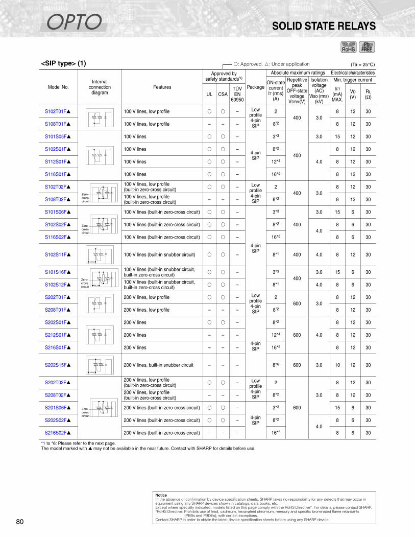
OPTO
80
SOLID STATE RELAYS
<SIP type> (1)
*1 to *6: Please refer to the next page.The model marked with
may not be available in the near future. Contact with SHARP for details before use.
Model No.Internal
connectiondiagram
Features
Approved by safety standards
*6
Package
Absolute maximum ratings
Electrical characteristics
ON-state current I
T
(rms)(A)
Repetitive peak
OFF-state voltageV
DRM
(V)
Isolation voltage
(AC)
Viso (rms)
(kV)
Min. trigger current
UL CSATÜV EN
60950
I
FT
(mA) MAX.
V
D
(V)
R
L
(
Ω
)
S102T01F
100 V lines, low profile
– Low profile 4-pinSIP
2400 3.0
8 12 30
S108T01F
100 V lines, low profile – – – 8
*2
8 12 30
S101S05F
100 V lines
–
4-pinSIP
3*
3
400
3.0 15 12 30
S102S01F
100 V lines
– 8*
2
4.0
8 12 30
S112S01F
100 V lines
– 12*
4
8 12 30
S116S01F
100 V lines
– 16*
5
8 12 30
S102T02F
100 V lines, low profile (built-in zero-cross circuit)
– Low profile 4-pinSIP
2400 3.0
8 12 30
S108T02F
100 V lines, low profile (built-in zero-cross circuit) – – – 8*
2
8 12 30
S101S06F
100 V lines (built-in zero-cross circuit)
–
4-pinSIP
3*
3
400
3.0 15 6 30
S102S02F
100 V lines (built-in zero-cross circuit)
– 8*
2
4.08 6 30
S116S02F
100 V lines (built-in zero-cross circuit)
– 16*
5
8 6 30
S102S11F
100 V lines (built-in snubber circuit)
– 8*
1
400 4.0 8 12 30
S101S16F
100 V lines (built-in snubber circuit, built-in zero-cross circuit)
– 3*
3
4003.0 15 6 30
S102S12F
100 V lines (built-in snubber circuit, built-in zero-cross circuit)
– 8*
1
4.0 8 6 30
S202T01F
200 V lines, low profile
– Low profile 4-pinSIP
2600 3.0
8 12 30
S208T01F
200 V lines, low profile – – – 8
*2
8 12 30
S202S01F
200 V lines
–
4-pinSIP
8*
2
600 4.0
8 12 30
S212S01F
200 V lines – – – 12*
4
8 12 30
S216S01F
200 V lines – – – 16*
5
8 12 30
S202S15F
200 V lines, built-in snubber circuit – – – 8*
6
600 3.0 10 12 30
S202T02F
200 V lines, low profile (built-in zero-cross circuit)
– Low profile 4-pinSIP
2
600
3.0
8 12 30
S208T02F
200 V lines, low profile (built-in zero-cross circuit) – – – 8*
2
8 12 30
S201S06F
200 V lines (built-in zero-cross circuit)
–
4-pinSIP
3*
3
15 6 30
S202S02F
200 V lines (built-in zero-cross circuit)
– 8*
2
4.08 6 30
S216S02F
200 V lines (built-in zero-cross circuit) – – – 16*
5
8 6 30
(Ta = 25°C): Approved, o: Under application
Zero-crosscircuit
Zero-crosscircuit
Zero-crosscircuit
Zero-crosscircuit
Notice
In the absence of confirmation by device specification sheets, SHARP takes no responsibility for any defects that may occur in equipment using any SHARP devices shown in catalogs, data books, etc. Except where specially indicated, models listed on this page comply with the RoHS Directive*. For details, please contact SHARP.*RoHS Directive: Prohibits use of lead, cadmium, hexavalent chromium, mercury and specific brominated flame retardants (PBBs and PBDEs), with certain exceptions.Contact SHARP in order to obtain the latest device specification sheets before using any SHARP device.

81
Opto
elec
tron
ics
SOLID STATE RELAYS
<SIP type> (2)
*1 Tc
&
88°C *2 Tc
&
80°C *3 Tc
&
100°C *4 Tc
&
70°C *5 Tc
&
60°C*6 Please refer to Specification Sheets for model numbers approved by safety standards.The model marked with
may not be available in the near future. Contact with SHARP for details before use.
Model No.Internal
connectiondiagram
Features
Approved by safety standards*
6
Package
Absolute maximum ratings
Electrical characteristics
ON-state current I
T
(rms)(A)
Repetitive peak
OFF-state voltageV
DRM
(V)
Isolation voltage
(AC)
Viso (rms)
(kV)
Min. trigger current
UL CSATÜV EN
60950
I
FT
(mA) MAX.
V
D
(V)
R
L
(
Ω
)
S202S11F
200 V lines (built-in snubber circuit)
–
4-pin SIP
8*
1
600 4.0 8 12 30
S202S12F
200 V lines (built-in snubber circuit, built-in zero-cross circuit)
– 8*
1
600 4.0 8 6 30
S202SE1F
200 V lines, reinforced isolation
8*
2
600 3.08 12 30
S216SE1F
– –
16*
5
8 12 30
S202SE2F
200 V lines (built-in zero-cross circuit), reinforced isolation
8*
2
600 3.08 6 30
S216SE2F
– –
16*
5
8 6 30
S102T01 series(Low profile 4-pin SIP)
S102S01 series(4-pin SIP)
(Ta = 25°C): Approved, o: Under application
Zero-crosscircuit
Zero-crosscircuit
Notice
In the absence of confirmation by device specification sheets, SHARP takes no responsibility for any defects that may occur in equipment using any SHARP devices shown in catalogs, data books, etc. Except where specially indicated, models listed on this page comply with the RoHS Directive*. For details, please contact SHARP.*RoHS Directive: Prohibits use of lead, cadmium, hexavalent chromium, mercury and specific brominated flame retardants (PBBs and PBDEs), with certain exceptions.Contact SHARP in order to obtain the latest device specification sheets before using any SHARP device.
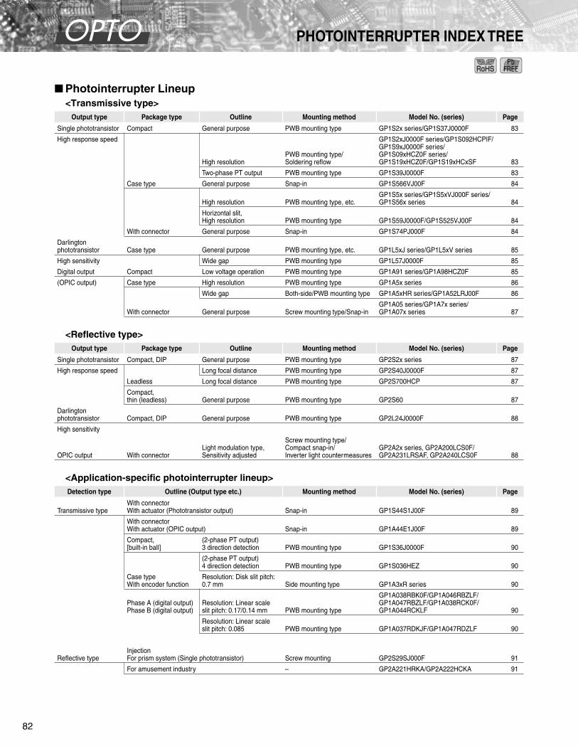
OPTO
82
PHOTOINTERRUPTER INDEX TREE
Photointerrupter Lineup
<Transmissive type>
<Reflective type>
<Application-specific photointerrupter lineup>
Output type Package type Outline Mounting method Model No. (series) Page
Single phototransistor Compact General purpose PWB mounting type GP1S2x series/GP1S37J0000F 83
High response speed
High resolutionPWB mounting type/Soldering reflow
GP1S2xJ0000F series/GP1S092HCPIF/GP1S9xJ0000F series/GP1S09xHCZ0F series/GP1S19xHCZ0F/GP1S19xHCxSF 83
Two-phase PT output PWB mounting type GP1S39J0000F 83
Case type General purpose Snap-in GP1S566VJ00F 84
High resolution PWB mounting type, etc.GP1S5x series/GP1S5xVJ000F series/GP1S56x series 84
Horizontal slit, High resolution PWB mounting type GP1S59J0000F/GP1S525VJ00F 84
With connector General purpose Snap-in GP1S74PJ000F 84
Darlington phototransistor Case type General purpose PWB mounting type, etc. GP1L5xJ series/GP1L5xV series 85
High sensitivity Wide gap PWB mounting type GP1L57J0000F 85
Digital output Compact Low voltage operation PWB mounting type GP1A91 series/GP1A98HCZ0F 85
(OPIC output) Case type High resolution PWB mounting type GP1A5x series 86
Wide gap Both-side/PWB mounting type GP1A5xHR series/GP1A52LRJ00F 86
With connector General purpose Screw mounting type/Snap-inGP1A05 series/GP1A7x series/GP1A07x series 87
Output type Package type Outline Mounting method Model No. (series) Page
Single phototransistor Compact, DIP General purpose PWB mounting type GP2S2x series 87
High response speed Long focal distance PWB mounting type GP2S40J0000F 87
Leadless Long focal distance PWB mounting type GP2S700HCP 87
Compact, thin (leadless) General purpose PWB mounting type GP2S60 87
Darlington phototransistor Compact, DIP General purpose PWB mounting type GP2L24J0000F 88
High sensitivity
OPIC output With connectorLight modulation type, Sensitivity adjusted
Screw mounting type/Compact snap-in/Inverter light countermeasures
GP2A2x series, GP2A200LCS0F/GP2A231LRSAF, GP2A240LCS0F 88
Detection type Outline (Output type etc.) Mounting method Model No. (series) Page
Transmissive typeWith connectorWith actuator (Phototransistor output) Snap-in GP1S44S1J00F 89
With connectorWith actuator (OPIC output) Snap-in GP1A44E1J00F 89
Compact, [built-in ball]
(2-phase PT output) 3 direction detection PWB mounting type GP1S36J0000F 90
(2-phase PT output) 4 direction detection PWB mounting type GP1S036HEZ 90
Case typeWith encoder function
Resolution: Disk slit pitch: 0.7 mm Side mounting type GP1A3xR series 90
Phase A (digital output)Phase B (digital output)
Resolution: Linear scale slit pitch: 0.17/0.14 mm PWB mounting type
GP1A038RBK0F/GP1A046RBZLF/GP1A047RBZLF/GP1A038RCK0F/GP1A044RCKLF 90
Resolution: Linear scale slit pitch: 0.085 PWB mounting type GP1A037RDKJF/GP1A047RDZLF 90
Reflective typeInjectionFor prism system (Single phototransistor) Screw mounting GP2S29SJ000F 91
For amusement industry – GP2A221HRKA/GP2A222HCKA 91
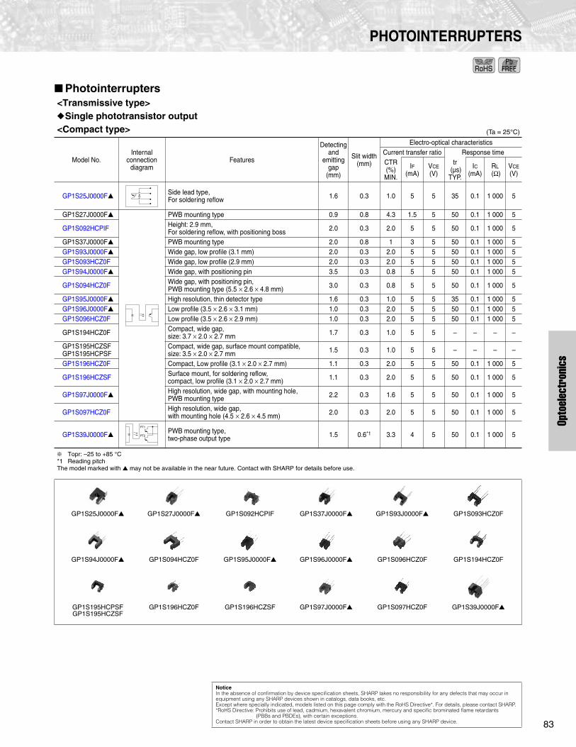
83
Opto
elec
tron
ics
PHOTOINTERRUPTERS
Photointerrupters
<Transmissive type>
Single phototransistor output<Compact type>
Topr: –25 to +85 °C*1 Reading pitchThe model marked with
may not be available in the near future. Contact with SHARP for details before use.
Model No.Internal
connectiondiagram
Features
Detecting and
emitting gap
(mm)
Slit width (mm)
Electro-optical characteristicsCurrent transfer ratio Response timeCTR (%)
MIN.
I
F
(mA)
V
CE
(V)
tr (µs) TYP.
I
C
(mA)
R
L
(
Ω
) V
CE
(V)
GP1S25J0000F
Side lead type, For soldering reflow 1.6 0.3 1.0 5 5 35 0.1 1 000 5
GP1S27J0000F
PWB mounting type 0.9 0.8 4.3 1.5 5 50 0.1 1 000 5
GP1S092HCPIF Height: 2.9 mm, For soldering reflow, with positioning boss 2.0 0.3 2.0 5 5 50 0.1 1 000 5
GP1S37J0000F
PWB mounting type 2.0 0.8 1 3 5 50 0.1 1 000 5GP1S93J0000F
Wide gap, low profile (3.1 mm) 2.0 0.3 2.0 5 5 50 0.1 1 000 5GP1S093HCZ0F Wide gap, low profile (2.9 mm) 2.0 0.3 2.0 5 5 50 0.1 1 000 5GP1S94J0000F
Wide gap, with positioning pin 3.5 0.3 0.8 5 5 50 0.1 1 000 5
GP1S094HCZ0F Wide gap, with positioning pin, PWB mounting type (5.5
×
2.6
×
4.8 mm) 3.0 0.3 0.8 5 5 50 0.1 1 000 5
GP1S95J0000F
High resolution, thin detector type 1.6 0.3 1.0 5 5 35 0.1 1 000 5GP1S96J0000F
Low profile (3.5
×
2.6
×
3.1 mm) 1.0 0.3 2.0 5 5 50 0.1 1 000 5GP1S096HCZ0F Low profile (3.5
×
2.6
×
2.9 mm) 1.0 0.3 2.0 5 5 50 0.1 1 000 5
GP1S194HCZ0F Compact, wide gap, size: 3.7
×
2.0
×
2.7 mm 1.7 0.3 1.0 5 5 – – – –
GP1S195HCZSFGP1S195HCPSF
Compact, wide gap, surface mount compatible, size: 3.5
×
2.0
×
2.7 mm 1.5 0.3 1.0 5 5 – – – –
GP1S196HCZ0F Compact, Low profile (3.1
×
2.0
×
2.7 mm) 1.1 0.3 2.0 5 5 50 0.1 1 000 5
GP1S196HCZSF Surface mount, for soldering reflow, compact, low profile (3.1
×
2.0
×
2.7 mm) 1.1 0.3 2.0 5 5 50 0.1 1 000 5
GP1S97J0000F
High resolution, wide gap, with mounting hole, PWB mounting type 2.2 0.3 1.6 5 5 50 0.1 1 000 5
GP1S097HCZ0F High resolution, wide gap, with mounting hole (4.5
×
2.6
×
4.5 mm) 2.0 0.3 2.0 5 5 50 0.1 1 000 5
GP1S39J0000F
PWB mounting type, two-phase output type 1.5 0.6
*1
3.3 4 5 50 0.1 1 000 5
GP1S25J0000F
GP1S27J0000F
GP1S092HCPIF GP1S37J0000F
GP1S93J0000F
GP1S093HCZ0F
GP1S94J0000F
GP1S094HCZ0F GP1S95J0000F
GP1S96J0000F
GP1S096HCZ0F GP1S194HCZ0F
GP1S195HCPSFGP1S195HCZSF
GP1S196HCZ0F GP1S196HCZSF GP1S97J0000F
GP1S097HCZ0F GP1S39J0000F
(Ta = 25°C)
PT1
PT2
Notice
In the absence of confirmation by device specification sheets, SHARP takes no responsibility for any defects that may occur in equipment using any SHARP devices shown in catalogs, data books, etc. Except where specially indicated, models listed on this page comply with the RoHS Directive*. For details, please contact SHARP.*RoHS Directive: Prohibits use of lead, cadmium, hexavalent chromium, mercury and specific brominated flame retardants (PBBs and PBDEs), with certain exceptions.Contact SHARP in order to obtain the latest device specification sheets before using any SHARP device.

OPTO
84
PHOTOINTERRUPTERS
<Case type>
Topr: –25 to +85 °C*1 High reliability types: GP1SQ51VJ00F, and GP1SQ52J000F are also available.
<With connector type>
Topr: –25 to +85 °C
Model No.Internal
connectiondiagram
Features
Detecting and
emitting gap
(mm)
Slit width (mm)
Electro-optical characteristicsCurrent transfer ratio Response timeCTR (%)
MIN.
I
F
(mA)
V
CE
(V)
tr (µs) TYP.
I
C
(mA)
R
L
(
Ω
) V
CE
(V)
GP1S566VJ00F Long case, snap-in mounting type 3.0 0.5 2.5 20 5 3 2 100 2
GP1S50J0000F High resolution, both-side mounting type 3.0 0.5 2.5 20 5 3 2 100 2
GP1S51VJ000F*
1
High resolution, side mounting type 3.0 0.5 2.5 20 5 3 2 100 2
GP1S52VJ000F*
1
High resolution, PWB mounting type 3.0 0.5 2.5 20 5 3 2 100 2
GP1S53VJ000F High resolution, PWB mounting type 5.0 0.5 2.5 20 5 3 2 100 2
GP1S54J0000F High resolution, with positioning pin, PWB mounting type 3.0 0.5 2.5 20 5 3 2 100 2
GP1S56TJ000F High resolution, with positioning pin, PWB mounting type 2.0 0.15 2.0 20 5 38 0.5 1 000 2
GP1S58VJ000F High resolution, with positioning pin, PWB mounting type 5.0 0.5 2.5 20 5 3 2 100 2
GP1S59J0000F High resolution, horizontal slit, with positioning pin, PWB mounting type 4.2 0.5 2.5 20 5 3 2 100 2
GP1S525VJ00FShort lead type with easy board mounting, horizontal slit, high precision positioning (lead: within ø1.2 mm)
5.0 0.5 3.25 20 10 3 2 100 2
GP1S566VJ00F GP1S50J0000F GP1S51VJ000F GP1S52VJ000F GP1S53VJ000F
GP1S54J0000F GP1S56TJ000F GP1S58VJ000F GP1S59J0000F GP1S525VJ00F
Model No.Internal
connectiondiagram
Features
Detecting and
emitting gap
(mm)
Slit width (mm)
Electro-optical characteristicsCurrent transfer ratio Response timeCTR (%)
MIN.
I
F
(mA)
V
CE
(V)
tr (µs) TYP.
I
C
(mA)
R
L
(
Ω
) V
CE
(V)
GP1S74PJ000F Snap-in mounting type with connectorApplicable to 3 kinds of thickness of mounting boards 5.0 0.5 2.5 20 5 3 2 100 2
GP1S74PJ000F
(Ta = 25°C)
(Ta = 25°C)
Notice
In the absence of confirmation by device specification sheets, SHARP takes no responsibility for any defects that may occur in equipment using any SHARP devices shown in catalogs, data books, etc. Except where specially indicated, models listed on this page comply with the RoHS Directive*. For details, please contact SHARP.*RoHS Directive: Prohibits use of lead, cadmium, hexavalent chromium, mercury and specific brominated flame retardants (PBBs and PBDEs), with certain exceptions.Contact SHARP in order to obtain the latest device specification sheets before using any SHARP device.
!

85
Opto
elec
tron
ics
PHOTOINTERRUPTERS
New product
Darlington phototransistor output<Case type>
Topr: –25 to +85 °C
OPIC type<Compact type>
Topr = –25 to +85°C*1 Resolution of detecting portionThe model marked with
may not be available in the near future. Contact with SHARP for details before use.
Model No.Internal
connectiondiagram
Features
Detecting and
emitting gap
(mm)
Slit width (mm)
Electro-optical characteristicsCurrent transfer ratio Response timeCTR (%)
MIN.
I
F
(mA)
V
CE
(V)
tr (µs) TYP.
I
C
(mA)
R
L
(
Ω
) V
CE
(V)
GP1L50J0000F High resolution, both-side mounting type 3.0 0.5 50 1 2 80 2 100 2
GP1L51J0000F High resolution, side mounting type 3.0 0.5 50 1 2 80 2 100 2
GP1L52VJ000F High resolution, PWB mounting type 3.0 0.5 50 1 2 80 2 100 2
GP1L53VJ000F High resolution, PWB mounting type 5.0 0.5 30 1 2 80 2 100 2
GP1L57J0000F Wide gap, PWB mounting type 10.0 1.8 70 1 2 130 2 100 2
GP1L50J0000F GP1L51J0000F GP1L52VJ000F GP1L53VJ000F GP1L57J0000F
Model No.Internal
connectiondiagram
Features
Detecting and
emitting gap
(mm)
Slit width (mm)
Electro-optical characteristicsThreshold input current Propagation delay timeI
FLH
(mA) MAX.
I
FHL
(mA) MAX.
V
CC
(V)
tPLH(µs) TYP.
t
PHL
(µs) TYP.
I
F
(mA)
R
L
(
Ω
) V
CC
(V)
GP1A91LRJ00F
Compact, PWB mounting, low operating voltage (1.4 V to 7.0 V)
1.2 (0.23)
*1
– 3.5 3 10.0 3.0 5 3 000 3
GP1A91LCJ00F
Compact, PWB mounting, low operating voltage (1.4 V to 7.0 V)
1.2 (0.23)
*1
– 3.5 3 10.0 3.0 5 2 500 3
GP1A98HCZ0F Compact, PWB mounting 3.0 0.5 8 – 3.3 to 24 10.0 2.0 10
3 900 to
20 000
3.3 to 24
GP1A91LRJ00F(GP1A91LCJ00F)
GP1A98HCZ0F
(Ta = 25°C)
“OPIC” (Optical IC) is a trademark of SHARP Corporation. An OPIC consists of alight-detecting element and signal-processing circuit integrated onto a single chip.( )
(Ta = 25°C)
Amplifier
(15 kΩ)
Amplifier
(15 kΩ)
Amplifier
Voltageregulator
Notice
In the absence of confirmation by device specification sheets, SHARP takes no responsibility for any defects that may occur in equipment using any SHARP devices shown in catalogs, data books, etc. Except where specially indicated, models listed on this page comply with the RoHS Directive*. For details, please contact SHARP.*RoHS Directive: Prohibits use of lead, cadmium, hexavalent chromium, mercury and specific brominated flame retardants (PBBs and PBDEs), with certain exceptions.Contact SHARP in order to obtain the latest device specification sheets before using any SHARP device.
"

OPTO
86
PHOTOINTERRUPTERS
<Case type>
Topr = –25 to +85°C
Model No.Internal
connectiondiagram
Features
Detecting and
emitting gap
(mm)
Slit width (mm)
Electro-optical characteristics
Threshold input current Propagation delay time
I
FLH
(mA) MAX.
I
FHL
(mA) MAX.
V
CC
(V)
tPLH(µs) TYP.
t
PHL
(µs) TYP.
I
F
(mA)
R
L
(
Ω
) V
CC
(V)
GP1A50HRJ00F Both-side mounting type 3.0 0.5 5 – 5 3 5 5 280 5
GP1A51HRJ00F Side mounting type 3.0 0.5 5 – 5 3 5 5 280 5
GP1A52HRJ00F PWB mounting type 3.0 0.5 5 – 5 3 5 5 280 5
GP1A53HRJ00F PWB mounting type 5.0 0.5 8 – 5 3 5 8 280 5
GP1A57HRJ00F PWB mounting type, with positioning pin 10.0 1.8 7 – 5 3 5 7 280 5
GP1A58HRJ00F PWB mounting type, with positioning pin 5.0 0.5 8 – 5 3 5 8 280 5
GP1A52LRJ00F PWB mounting type 3.0 0.5 – 5 5 5 3 5 280 5
GP1A50HRJ00F GP1A51HRJ00F GP1A52LRJ00F (GP1A52HRJ00F)
GP1A53HRJ00FGP1A58HRJ00F with positioning pin
GP1A57HRJ00F
(Ta = 25°C)
Amplifier
Voltageregulator
Amplifier
Voltageregulator
Notice
In the absence of confirmation by device specification sheets, SHARP takes no responsibility for any defects that may occur in equipment using any SHARP devices shown in catalogs, data books, etc. Except where specially indicated, models listed on this page comply with the RoHS Directive*. For details, please contact SHARP.*RoHS Directive: Prohibits use of lead, cadmium, hexavalent chromium, mercury and specific brominated flame retardants (PBBs and PBDEs), with certain exceptions.Contact SHARP in order to obtain the latest device specification sheets before using any SHARP device.
#

87
Opto
elec
tron
ics
PHOTOINTERRUPTERS
OPIC type<With 3-pin connector terminal>
Topr: –20 to +75°C
Photointerrupters
<Reflective type>
Single Phototransistor output<Compact>
Topr: –25 to +85°C *1 Detection area
Model No.Internal
connectiondiagram
Features
Detecting and
emitting gap
(mm)
Slit width (mm)
Electro-optical characteristicsSupply voltage
V
CC
(V)
Low level output voltageV
OL
(V)
MAX.
Light cut-off
I
OL
(mA) V
CC
(V) MIN. MAX.
GP1A05AJ000Fw
ith 3
-pin
con
nect
orEither-side mounting type 5.0 0.5 4.5 5.5 0.35 No 16 5
GP1A05A2J00F Either-side mounting type 5.0 0.5 4.5 5.5 0.35 No 16 5
GP1A05A5J00F Either-side mounting type 5.0 0.5 4.5 5.5 0.35 No 16 5
GP1A73AJ000F Compact, snap-in mounting type 5.0 0.5 4.5 5.5 0.35 No 4 5
GP1A073LCSCompact, snap-in mounting type, low voltage operation
5.0 0.5 2.7 5.5 0.35 No 4 5
GP1A75EJ000F Either-side mounting type 5.0 0.5 4.5 5.5 0.35 Yes 16 5
GP1A05EJ000FEither-side mounting typeScrew mounting type
5.0 0.5 4.5 5.5 0.4 Yes 16 5
GP1A05E2J00F 5.0 0.5 4.5 5.5 0.4 Yes 16 5
GP1A05AJ000F(GP1A05EJ000F)
GP1A05A2J00F(GP1A05E2J00F)
GP1A05A5J00F GP1A73AJ000F, GP1A073LCS GP1A75EJ000F
Model No.Internal
connectiondiagram
FeaturesFocal
distance (mm)
Electro-optical characteristicsCurrent transfer ratio Response time
CTR (%) MIN.
I
F
(mA) V
CE
(V) tr (µs) TYP.
I
C
(mA) R
L
(
Ω
) V
CE
(V)
GP2S24J0000F Compact (DIP), visible light cut-off 0.7 0.5 4 2 20 0.1 1 000 2
GP2S27J0000F Compact, allow reflow soldering, visible light cut-off 0.7 0.5 4 2 20 0.1 1 000 2
GP2S40J0000F Compact, long focal distance, visible light cut-off 3 2.5 20 5 50 0.1 1 000 2
GP2S700HCP Compact, long focal distance, surface mounting leadless type 3 1.5 4 2 20 0.1 1 000 2
GP2S60 Thin (3.2
×
1.7
×
t: 1.1 mm), leadless type (0.5) 1.75
*1
TYP. 4 2 20 0.1 1 000 2
GP2S24J0000F GP2S27J0000F GP2S40J0000F GP2S700HCP GP2S60
“OPIC” (Optical IC) is a trademark of SHARP Corporation. An OPIC consists of alight-detecting element and signal-processing circuit integrated onto a single chip.( )
(Ta = 25°C)
Amplifier
Voltageregulator
Amplifier
Voltageregulator
Amplifier
Voltageregulator
Amplifier
Voltageregulator
15 kΩ
(Ta = 25°C)
Notice
In the absence of confirmation by device specification sheets, SHARP takes no responsibility for any defects that may occur in equipment using any SHARP devices shown in catalogs, data books, etc. Except where specially indicated, models listed on this page comply with the RoHS Directive*. For details, please contact SHARP.*RoHS Directive: Prohibits use of lead, cadmium, hexavalent chromium, mercury and specific brominated flame retardants (PBBs and PBDEs), with certain exceptions.Contact SHARP in order to obtain the latest device specification sheets before using any SHARP device.

OPTO
88
PHOTOINTERRUPTERS
Darlington Phototransistor output<Compact>
OPIC output<With 3-pin connector terminal>
Topr: –10 to +60°C (GP2A22J0000F, GP2A25J0000F, GP2A25BJ000F) *1 Smoothing value R
L
=
∞
The model marked with
may not be available in the near future. Contact with SHARP for details before use.
Model No.Internal
connectiondiagram
FeaturesFocal
distance (mm)
Electro-optical characteristicsCurrent transfer ratio Response time
CTR (%) MIN.
I
F
(mA) V
CE
(V) tr (µs) TYP.
I
C
(mA) R
L
(
Ω
) V
CE
(V)
GP2L24J0000F Compact (DIP), visible light cut-off 0.7 12.5 4 2 80 10 100 2
GP2L24J0000F
Model No.Internal
connectiondiagram
Features
Optimum detecting distance
(mm)
Electro-optical characteristics
Supply voltage
V
CC
(V)
Dissipation current
Low level output voltage
I
CC
(mA) MAX.
V
CC
(V)
V
OL
(V)MAX.
V
CC
(V) MIN. MAX.
OP
IC o
utpu
t
GP2A22J0000F
(Following diagram)
Multi types of paper detectable, light modulation type, with connector, sensitivity adjusted 9 to 15 4.75 5.25 30*
1
5 0.4 5
GP2A200LCS0F Multi types of paper detectable, light modulation type, with connector, sensitivity adjusted 5 to 15 4.75 5.25 30*
1
5 0.4 5
GP2A240LCS0F Improved light-resistance characteristic for inverter lighting (500 lx), light modulation type, connector output 5 to 15 4.75 5.25 30*
1
5 0.4 5
GP2A250LCS0FStatic electricity resistant, improved light-resistance characteristic for inverter lighting (500 lx), light modulation type, connector output
5 to 15 4.75 5.25 30*
1
5 0.4 5
GP2A25J0000F Multi types of paper detectable, light modulation type, with connector, sensitivity adjusted 3 to 7 4.75 5.25 30*
1
5 0.4 5
GP2A231LRSAF Compact, Hook type, Multi types of paper detectable, light modulation type, with connector, sensitivity adjusted 3 to 7 4.75 5.25 20*
1
5 0.4 5
GP2A25NJJ00FMulti types of paper detectable, light modulation type, sensitivity adjusted, applicable to inverter fluorescent lamp, built-in visible light cut filter
3 to 6 4.75 5.25 30*
1
5 0.4 5
GP2A25BJ000F Multi types of paper detectable, light modulation type, with connector, sensitivity adjusted 3 to 7 4.75 5.25 30*
1
5 0.4 5
GP2A28AJ000FMulti types of paper detectable, light modulation type, with connector, sensitivity adjusted, detecting portion with flat configuration
3 to 7 4.75 5.25 30*
1
5 0.4 5
[Internal connection diagram]
GP2A22J0000F GP2A25J0000FGP2A25NJ, GP2A28AJ000F, GP2A200LCS0F, GP2A240LCS0F
GP2A250LCS0F GP2A25BJ000F GP2A231LRSAF
(Ta = 25°C)
“OPIC” (Optical IC) is a trademark of SHARP Corporation. An OPIC consists of alight-detecting element and signal-processing circuit integrated onto a single chip.( )
(Ta = 25°C)
AmplifierComparatorVoltage regulatorDemodulator
Synchronous detectorOscillator
Notice
In the absence of confirmation by device specification sheets, SHARP takes no responsibility for any defects that may occur in equipment using any SHARP devices shown in catalogs, data books, etc. Except where specially indicated, models listed on this page comply with the RoHS Directive*. For details, please contact SHARP.*RoHS Directive: Prohibits use of lead, cadmium, hexavalent chromium, mercury and specific brominated flame retardants (PBBs and PBDEs), with certain exceptions.Contact SHARP in order to obtain the latest device specification sheets before using any SHARP device.

89
Opto
elec
tron
ics
PHOTOINTERRUPTERS
Photointerrupters for Specific Applications
Transmissive type<Single phototransistor output type with actuator and 3-pin connector terminal>
Topr: –25 to +75 °C*1 Operating voltage: 4.5 to 5.5 V
<OPIC type with actuator and 3-pin connector terminal>
Topr: –25 to +75 °C*1 Operating voltage: 4.5 to 5.5 V
Model No.Internal
connectiondiagram
Features
Actuator lever starting torque
(Initial)MAX.
Electro-mechanical characteristics*
1
Light beam interrupted Light beam uninterrupted
Dissipation current
Collector current
Dissipation current
Collector currentI
CC1
(mA)
V
CC
(V)
I
C1
(µA) V
CC
(V) V
O
(V) I
CC2
(mA)
V
CC
(V) I
C2
(mA)
V
CC
(V)
V
O
(V)
GP1S44S1J00F Spring lever type actuatorUnited with connector
1
×
10
-4
N•m or less
20MAX. 5 50
MAX. 5 5 20MAX. 5 0.25
MIN. 5 5
GP1S44S1J00F
Model No.Internal
connectiondiagram
Features
Absolute maximum
ratings
Electro-mechanical
characteristicsElectro-mechanical characteristics*
1
Supply voltage
V
CC
(V)
Output current
I
OL
(mA)
Actuator lever
starting torque
Light beam interrupted Light beam uninterrupted
Dissipation current
Low level output voltage
Dissipation current
High level output voltage
I
CCL
(mA)
V
CC
(V)
V
OL
(V) V
CC
(V)
I
OL
(mA)
I
CCH
(mA) V
CC
(V)
V
OH
(V) V
CC
(V)
R
L
(k
Ω
)
GP1A44E1J00FSpring lever type actuator, United with connector
10 50 1
×
10
–4
N•m or less
20MAX. 5 0.4
MAX. 5 16 20MAX. 5
Vcc
×
0.9
MIN. 5 47
GP1A44E1J00F
(Ta = 25°C)
(Ta = 25°C)
Amplifier
Voltageregulator
15 kΩ
Notice
In the absence of confirmation by device specification sheets, SHARP takes no responsibility for any defects that may occur in equipment using any SHARP devices shown in catalogs, data books, etc. Except where specially indicated, models listed on this page comply with the RoHS Directive*. For details, please contact SHARP.*RoHS Directive: Prohibits use of lead, cadmium, hexavalent chromium, mercury and specific brominated flame retardants (PBBs and PBDEs), with certain exceptions.Contact SHARP in order to obtain the latest device specification sheets before using any SHARP device.

OPTO
90
PHOTOINTERRUPTERS
<Compact, 2-phase phototransistor output type>
Topr: –25 to +85 °CThe model marked with
may not be available in the near future. Contact with SHARP for details before use.
<Case type, with encoder function>
*1 High precision read and low affection of angle error from vibration thanks to the multi-segment PD system *2 Duty ratio: 50±10%, phase difference: 90±30°*3 Duty ratio: 50±20%, phase difference: 90±45°The model marked with
may not be available in the near future. Contact with SHARP for details before use.
Model No.Internal
connectiondiagram
Features
Electro-optical characteristicsCurrent transfer ratio Response timeCTR (%)
MIN.
I
F
(mA)
V
CE
(V)
tr (µs) TYP.
I
C
(mA)
R
L
(
Ω
) V
CE
(V)
GP1S36J0000F
Built-in ball (2 phase output), compact, PWB mounting type
1.2 5 5 50 0.1 1 000 5
GP1S036HEZ
Built-in ball (2 phase output), compact, PWB mounting type, 4-direction detection
1.1 5 5 50 0.1 1 000 5
GP1S36J0000F GP1S036HEZ
Model No.
Absolute maximum ratings
Electro-optical characteristics
Vcc (V)
Topr (°C)
Operating voltage Vcc (V)
Output signal ResolutionResponse frequency Dissipation current
(output side) Icc (mA) MAX.
(kHz) MAX. I
F
(mA)
GP1A30RJ000F
7 0 to +70 4.5 to 5.5
Phase A (Digital output)Phase B (Digital output)
Disk slit pitch 0.7 (mm) 5 30 20
GP1A038RBK0F*
1,
*
3
7 0 to +70 2.7 to 5.5 Linear scale slit pitch 0.17 (mm) 20 11 5
GP1A038RCK0F*
1,
*
3
7 0 to +70 2.7 to 5.5 Linear scale slit pitch 0.14 (mm) 20 11 5
GP1A037RDKJF*
1,
*
3
7 0 to +70 2.7 to 5.5 Linear scale slit pitch 0.0847 (mm) 40 25 10
GP1A044RCKLF*
1
— –10 to +60 2.7 to 5.5 Linear scale slit pitch 0.14 (mm) 20 15 5
GP1A046RBZLF*
1
— –10 to +60 2.7 to 5.5 Linear scale slit pitch 0.17 (mm) 20 20 5
GP1A047RBZLF — 0 to +60 2.7 to 5.5 Linear scale slit pitch 0.17 (mm) 20 20 7
GP1A047RDZLF — –10 to +60 2.7 to 5.5 Linear scale slit pitch 0.0847 (mm) 120 20 7
GP1A30RJ000F
GP1A044RCKLF GP1A038RBK0F(GP1A038RCK0F, GP1A037RDKJF)
GP1A046RBZLF GP1A047RBZLF(GP1A047RDZLF)
(Ta = 25°C)
PT1
PT2
(Ta = 25°C)
Notice
In the absence of confirmation by device specification sheets, SHARP takes no responsibility for any defects that may occur in equipment using any SHARP devices shown in catalogs, data books, etc. Except where specially indicated, models listed on this page comply with the RoHS Directive*. For details, please contact SHARP.*RoHS Directive: Prohibits use of lead, cadmium, hexavalent chromium, mercury and specific brominated flame retardants (PBBs and PBDEs), with certain exceptions.Contact SHARP in order to obtain the latest device specification sheets before using any SHARP device.

91
Opto
elec
tron
ics
PHOTOINTERRUPTERS
Reflective type<Case type, phototransistor output>
Topr: –25 to +85°C *1 Space between prism and sensor is 8 mm.
<For the amusement industry>
*1 Used together with interface IC for control (IR3N184)
Model No.Internal
connectiondiagram
FeaturesFocal
distance (mm)
Electro-optical characteristicsCurrent transfer ratio Response time
CTR (%) MIN.
I
F
(mA) V
CE
(V) tr (µs) TYP.
I
C
(mA) R
L
(
Ω
) V
CE
(V)
GP2S29SJ000F Long focal distance (with prism system), compact, screw mounting type
*1
1.0
*1
20 5 38 0.5 1 000 2
GP2S29SJ000F
Model No. FeaturesElectro-optical characteristics
Supply voltage Vcc
Dissipation current Response frequency f (Hz)Icc (mA)
GP2A221HRKA Employs reflective type, pinball detector, connector with lock 4.5 to 15 MAX. 10 MAX. 500
GP2A222HCKA Employs reflective type, pinball detector, connector with lockIn conjunction with an IC, detects beam interuption
*1
4.5 to 16.5 MAX. 10 MAX. 500
GP2A221HRKA(GP2A222HCKA)
(Ta = 25°C)
(Ta = 25°C)
Notice
In the absence of confirmation by device specification sheets, SHARP takes no responsibility for any defects that may occur in equipment using any SHARP devices shown in catalogs, data books, etc. Except where specially indicated, models listed on this page comply with the RoHS Directive*. For details, please contact SHARP.*RoHS Directive: Prohibits use of lead, cadmium, hexavalent chromium, mercury and specific brominated flame retardants (PBBs and PBDEs), with certain exceptions.Contact SHARP in order to obtain the latest device specification sheets before using any SHARP device.

OPTO
92
PHOTOTRANSISTOR INDEX TREE
Phototransistor Lineup
The model marked with
may not be available in the near future. Contact with SHARP for details before use.
Package Output type FeaturesHalf
sensitivity angle
Model No.
Standard Visible light cut-off
Epoxy resin with lens(ø3 mm) Single phototransistor General purpose ±20° PT380 PT380F
Darlington phototransistor High sensitivity ±20° PT381 PT381F
Epoxy resin with lens Single phototransistor General purpose/Narrow acceptance ±13° PT480E00000F PT480FE0000F
Compact, thin ±35° PT4800E0000FPT4800FE000F / PT4850FE000F
Darlington phototransistor High sensitivity/Narrow acceptance ±13° PT481E00000F PT481FE0000F
High sensitivity/Narrow acceptance/Long lead ±13° — PT483F1E000F
High sensitivity/Compact, thin ±35° PT4810E0000F PT4810FJE00F
High sensitivity/Intermediate acceptance ±40° — PT491FE0000F
High sensitivity/Intermediate acceptance/Long lead ±40° — PT493FE0000F
TO-18 Single phototransistor Narrow acceptance ±6° PT501
—
Narrow acceptance/With base terminal ±6° PT510
—
Darlington phototransistor Narrow acceptance/With base terminal ±6° PT550
—
Wide acceptance/With base terminal ±50° PT550F
—
Surface mounting leadless type Single phototransistor Compact ±60° PT600T —
Compact (surface mounting type) ±70° PT200MC0NP —
Compact(infrared cut type) ±60° PT202MR0MP1 —
Compact(side view/top view mounting possible) ±15° PT100MC0MP PT100MF0MP
Darlington phototransistor Compact ±60° PT601T —
Compact(side view/top view mounting possible) ±15° — PT100MF1MP

93
Opto
elec
tron
ics
PHOTOTRANSISTORS
Phototransistors
*1 Visible light cut-off type *2 Infrared cut-off typeNote) Some products are handled by the Compound Semiconductor Division.The model marked with
may not be available in the near future. Contact with SHARP for details before use.
Type Model No. Package
Absolute maximum ratings Ic (mA) I
CEO
(A) Dq(°)
TYP.
λ
p (nm) TYP.
V
CEO
(V)
P
C
(mW)Topr (°C) MIN. MAX. V
CE
(V)
Ee (mW/cm
2
) MAX. V
CE
(V)
Sin
gle
PT380ø3 epoxy resin
35 50 –25 to +85 0.16 1.17 5 Ev, 100 Ix 1
×
10
–7
20 ±20 800
PT380F*
1
35 50 –25 to +85 0.095 0.9 5 Ev, 100 Ix 1
×
10
–7
20 ±20 860
PT600T
Surface mounting leadless type
35 50 –25 to +85 0.7 TYP. 3.5 5 5 1
×
10
–7
20 ±60 880
PT200MC0NP 50 50 –25 to +85 0.016 0.059 5 0.1 1
×
10
–7
20 ±70 930
PT202MR0MP1*
2
5 5 –30 to +85 — TYP. 0.043 1.5 Ev, 100 Ix 1
×
10
–7
1.5 ±60 620
PT100MC0MP 35 75 –30 to +85 1.7 5.1 5 1 1
×
10
–7
20 ±15 900
PT100MF0MP*
1
35 75 –30 to +85 1.15 3.45 5 1 1
×
10
–7
20 ±15 910
PT480E00000F
Epoxy resin with lens
35 75 –25 to +85 0.4 TYP. 1.7 5 1 1
×
10
–7
20 ±13 800
PT480FE0000F*
1
35 75 –25 to +85 0.25 TYP. 0.8 5 1 1
×
10
–7
20 ±13 860
PT4800E0000F 35 75 –25 to +85 0.12 TYP. 0.4 5 1 1
×
10
–7
20 ±35 800
PT4800FE000F*
1
35 75 –25 to +85 0.08 TYP. 0.25 5 1 1
×
10
–7
20 ±35 860
PT4850FE000F*
1
35 75 –25 to +85 0.12 0.56 5 1 1
×
10
–7
20 ±35 860
PT501
TO-18 45 75 –25 to +125 2.5 TYP. 10 5 10 1
×
10
–7
30 ±6 800
PT510
35 75 –25 to +125 2.5 TYP. 20.0 5 10 1
×
10
–7
30 ±6 800
Dar
lingt
on
PT381ø3 epoxy resin
35 50 –25 to +85 0.12 1.5 10 Ev, 2 Ix 1
×
10
–6
10 ±20 800
PT381F*
1
35 50 –25 to +85 0.07 1.08 10 Ev, 2 Ix 1
×
10
–6
10 ±20 860
PT481E0000F
Epoxy resin with lens
35 75 –25 to +85 1.5 25 2 0.1 1
×
10
–6
10 ±13 800
PT481FE0000F*
1
35 75 –25 to +85 0.9 27 2 0.1 1
×
10
–6
10 ±13 860
PT4810E0000F 35 75 –25 to +85 0.45 7.0 2 0.1 1
×
10
–6
10 ±35 800
PT4810FJE00F*
1
35 75 –25 to +85 0.27 6.0 2 0.1 1
×
10
–6
10 ±35 860
PT483F1E000F*
1
35 75 –25 to +85 1.5 4.0 2 0.1 1
×
10
–6
10 ±13 860
PT491FE0000F*
1
35 75 –25 to +85 0.2 0.8 2 Ev, 2 Ix 1
×
10
–6
10 ±40 860
PT493FE0000F*
1
35 75 –25 to +85 0.2 0.8 2 Ev, 2 Ix 1
×
10
–6
10 ±40 860
PT550
TO-1835 150 –25 to +125 3 TYP. 20.0 5 0.1 1
×
10
–6
10 ±6 800
PT550F
35 150 –25 to +125 3 TYP. 20.0 5 1.0 1
×
10
–6
10 ±50 800
PT601T Leadless chip type 35 50 –25 to +85 0.03 0.3 10 0.01 1
×
10
–6
10 ±60 880
PT100MF1MP*
1
Surface mounting leadless type 35 75 –30 to +85 0.2 1.2 5 0.01 1
×
10
–6
10 ±15 860
PT600T(PT601T)
PT200MC0NP PT202MR0MP1 PT100MF0MPPT100MF1MP, PT100MC0MP: Transparent resin
PT380PT380F, PT381 PT381F
PT480E00000FPT480FE0000F, PT481E00000F, PT481FE0000F
PT4800E0000FPT4800FE000F,PT4810E0000F,PT4810FJ00F,PT4810FJE00F,PT4850FE000F
PT483F1E000F PT501
PT510
(PT550
)PT491FE0000F PT493FE0000F PT550F
(Ta = 25°C)
Notice
In the absence of confirmation by device specification sheets, SHARP takes no responsibility for any defects that may occur in equipment using any SHARP devices shown in catalogs, data books, etc. Except where specially indicated, models listed on this page comply with the RoHS Directive*. For details, please contact SHARP.*RoHS Directive: Prohibits use of lead, cadmium, hexavalent chromium, mercury and specific brominated flame retardants (PBBs and PBDEs), with certain exceptions.Contact SHARP in order to obtain the latest device specification sheets before using any SHARP device.

OPTO
94
PHOTODIODES
PIN Photodiodes
*1 Visible light cut-off type *2 Tape packaging type (PD412TNE00F)The model marked with
may not be available in the near future. Contact with SHARP for details before use.
PSD (Position Sensitive Detector)
Custom-made products (detecting portion changed products) are also available.The model marked with
may not be available in the near future. Contact with SHARP for details before use.
Blue Sensitive Photodiodes
Model No. Features Package (Material)
Active area
(mm
2
)
Topr (°C)
Isc (µA)MIN.
Id (A)
MAX.
tr, tf (µs)TYP.
λ
p (nm) TYP.
Ev (Ix)
V
R
(V)V
R
(V)R
L
(k
Ω
)
PD49PIE0000F
*
1
PIN type
Visible light cut-off epoxy resin 7.73 –25 to +85 2.4 100 3
×
10
–8
10 0.2 10 1 1 000
PD410PI2E00F*
1
Visible light cut-off epoxy resin with condenser (lens) 3.31 –25 to +85 2.5 100 1
×
10
–8
10 0.2 10 1 1 000
PD411PI2E00F Epoxy resin with transparent condenser (lens) 3.31 –25 to +85 5.0 100 1
×
10
–8
10 0.2 10 1 960
PD412PI2E00F*
2
Epoxy resin with transparent condenser (lens) 3.31 –25 to +85 3.5 100 1
×
10
–8
10 0.25 10 1 800
PD413PI2E00F*
1
PIN typeIrDA1.0
Visible light cut-off epoxy resin with condenser (lens) 3.31 –25 to +85 MIN. 4.5
(TYP. 5.4) 100 1
×
10
–8
10 0.2 10 1 960
PD60T Chip device type Transparent resin – –25 to +85 TYP. 4 1 000 1
×
10
–8
10 0.1 10 1 960
PD100MC0MP Surface mounting leadless type
Transparent epoxy resin board with lens – –30 to +85 0.6 100 1
×
10
–8
10 0.01 15 0.18 820
PD100MF0MP*
1
Surface mounting leadless type
Visible light cut-off epoxy resin board with lens – –30 to +85 0.4 100 1
×
10
–8
10 0.01 15 0.18 850
PD49PIE0000F
PD410PIE00FPD411PI2E00F: transparent; PD412PI2E00F: transparent,PD413PI2E00F
PD60T PD100MC0MP(PD100MF0MP: black)
Model No. Features Package (Material)
Active area(mm
2
)Topr (°C)
I
L
(µA) MIN.
tr, tf (µs) TYP.
Position detection
error(µm) MAX.
Ev (Ix) (k
Ω
) TYP.
V
R
(V)V
R
(V)R
L
(k
Ω
)
PD3122FE000F
Position sensitive detector With mounting hole
Visible light cut-off epoxy resin
1.2 (1.0
×
1.2 mm) –25 to +85 6.4 1 000 110 to 170 1 5 1 1 ±25
PD3122FE000F
Model No. Features Package (Material)
Active area(mm
2
)Topr (°C)
Isc (µA) MIN.
I
d
(A)
MAX.
λ
p (nm) TYP.
Ev (Ix)
V
R
(V)
BS520E0F Planer type Resin (black) 5.34 –20 to +60 0.4 100 1
×
10
–11
1 560
BS520E0F(with filter)
(Ta = 25°C)
(Ta = 25°C)
Interelectrode resistance
(Ta = 25°C)
Notice
In the absence of confirmation by device specification sheets, SHARP takes no responsibility for any defects that may occur in equipment using any SHARP devices shown in catalogs, data books, etc. Except where specially indicated, models listed on this page comply with the RoHS Directive*. For details, please contact SHARP.*RoHS Directive: Prohibits use of lead, cadmium, hexavalent chromium, mercury and specific brominated flame retardants (PBBs and PBDEs), with certain exceptions.Contact SHARP in order to obtain the latest device specification sheets before using any SHARP device.
!

OPTO
95
Opto
elec
tron
ics
OPIC LIGHT DETECTORS
New product
Laser Power Monitoring Photodiodes for Optical Disc System
RGB Color Sensor
Ambient Light Sensors
Model No. Features Package (Material)
Active area(mm)
Topr (°C)
Isc (mA) TYP.
I
d
(A)
MAX.
λ
p (nm) TYP.
Ev (Ix)
V
R
(V)
PD101SC0SS0F High response speed(cut-off frequency: 400 MHz) Transparent epoxy resin ø0.8 –25 to +85 450 100 1
×
10
–9
5 820
PD101SC0SS0F
Model No. Features PackagePeak sensitivity wavelength
(nm)Light receiving sensitivity
(A/W) TYP. Topr (°C)
Blue Green Red Blue Green Red
PD30CMC31MZ
RGB 3-color LED compatible 3PD structureFilter-on chip structure allows for both infrared light reducing characteristics and a more com-pact size (1.1 mm thick)
Surface mounting 3 x 4 mm 460 540 620 0.18 0.23 0.16 –40 to +85
PD30CMC31MZ
Model No. Type Package
Absolute maximum ratings Electro-optical characteristics
V
CC
(V)P
(mW)I
O
(mA)
Topr (°C)
E
VLH
E
VHL
t
PLH
t
PHL
(Ix) MAX.
(Ix) MAX.
V
CC
(V)(µs) TYP.
(µs) TYP.
V
CC
(V)E
V
(Ix)R
L
(
Ω
)
IS485E Built-in schmidt trigger circuit, amplifier and voltage regulator
Transparent epoxy resin with condenser (lens)
–0.5 to +17 175 50 –25 to +85 – 35 5 5 3 5 50 280
IS486E –0.5 to +17 175 50 –25 to +85 35 – 5 3 5 5 50 280
IS485E(IS486E)
(Ta = 25°C)
(Ta = 25°C)
(Ta = 25°C)“OPIC” (Optical IC) is a trademark of the SHARP Corporation. An OPIC consists of alight-detecting element and signal-processing circuit integrated onto a single chip.( )
Notice
In the absence of confirmation by device specification sheets, SHARP takes no responsibility for any defects that may occur in equipment using any SHARP devices shown in catalogs, data books, etc. Except where specially indicated, models listed on this page comply with the RoHS Directive*. For details, please contact SHARP.*RoHS Directive: Prohibits use of lead, cadmium, hexavalent chromium, mercury and specific brominated flame retardants (PBBs and PBDEs), with certain exceptions.Contact SHARP in order to obtain the latest device specification sheets before using any SHARP device.
"

OPTO
96
OPIC LIGHT DETECTORS
<Low-voltage operation>
<Model employing a light modulating system>
*1 IS471FE is less susceptible to disturbing effects thanks to the light modulation system*2 Vcc = 5 V*3 Straight lead type (IS471FSE) is also available.
<For laser beam printers (laser origin detection)>
Model No. Type Package
Absolute maximum ratings Electro-optical characteristics
P(mW)
I
O
(mA)
Topr (°C)
Operating supply
voltage (V)
E
VLH
E
VHL
t
PHL
t
PLH
(Ix) MAX.
(Ix) MAX.
V
CC
(V)(µs) TYP.
(µs) TYP.
V
CC
(V)E
V
(Ix)R
L
(
Ω
)
IS489E Built-in Schmidt trigger circuit and amplifier
Transparent epoxy resin with condenser (lens)
80 2 –25 to +85 1.4 to 7.0 – 15 3 1.3 8.5 3 125 3 000
IS489E
Model No. Type Package
Absolute maximum ratings Electro-optical characteristics*
2
Externaldisturbing light
illuminanceE
VDX
(Ix) TYP.V
CC
(V)P
(mW)I
O
(mA)
Topr (°C)
V
OL
(V) MAX.
V
OH
(V) MIN.
t
PLH
t
PHL
(µs) TYP.
(µs) TYP.
V
CC
(V)R
L
(
Ω
)
IS471FE*
1,
*
3
Built-in pulse driver circuit at the emitter side, synchronous detector circuit, amplifier circuit and demodulator circuit
Visible light cut-off epoxy resin
–0.5 to +16 250 50 –25 to +60 0.35 4.97 400 400 5 280 7 000
IS471FE
Model No. Type Package
Electro-optical characteristicsRecommended supply
voltageV
CC
(V)
V
OH
(V) MIN.
V
OL
(V) MAX.
H
→
L delay time variation
∆
t
PHL
(ns) MAX.
GA220T2L1IZ 2PD, differential type Transparent epoxy resin 18-pin 4.5 to 5.5 4.9 0.6 ±8.5
GA220T2L1IZ
(Ta = 25°C)
(Ta = 25°C)
(Ta = 25°C)
Notice
In the absence of confirmation by device specification sheets, SHARP takes no responsibility for any defects that may occur in equipment using any SHARP devices shown in catalogs, data books, etc. Except where specially indicated, models listed on this page comply with the RoHS Directive*. For details, please contact SHARP.*RoHS Directive: Prohibits use of lead, cadmium, hexavalent chromium, mercury and specific brominated flame retardants (PBBs and PBDEs), with certain exceptions.Contact SHARP in order to obtain the latest device specification sheets before using any SHARP device.
#
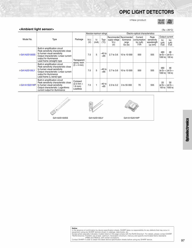
97
Opto
elec
tron
ics
OPIC LIGHT DETECTORS
New product
<Ambient light sensor>
Model No. Type Package
Absolute maximum ratings
Electro-optical characteristics
V
CC
(V)I
O
(mA)
Topr (°C)
Recommended supply voltage
V
CC
(V)
Recommended illuminance
range
Ex (lx)
Current consumption
Icc (µA) TYP.
Peak sensitivity
wavelength
λ
p (nm)
Output currentIo
1
(µA) TYP.
Io
2
(µA) TYP.
GA1A2S100SS
Built-in amplification circuitPeak sensitivity characteristic close to human visual sensitivityOutput characteristic: Linear current output for illuminanceLead frame (straight) type Transparent
epoxy resin (3
×
4 mm)
7.0 5 –40 to +85 2.7 to 3.6 10 to 10 000 500 555
480
(at Ev = 1000 lx)
48
(at Ev = 100 lx)
GA1A2S100LY
Built-in amplification circuitPeak sensitivity characteristic close to human visual sensitivityOutput characteristic: Linear current output for illuminanceLead frame (L bend) type
7.0 5 –40 to +85 2.7 to 3.6 10 to 10 000 500 555
480
(at Ev = 1000 lx)
48
(at Ev = 100 lx)
GA1A1S201WP
Built-in amplification circuitPeak sensitivity characteristic close to human visual sensitivityOutput characteristic: Logarithmic current output for illuminance
Compact (2.0 mm
×
1.6 mm) Leadless
7.0 1 –40 to +85 2.3 to 3.2 3 to 55 000 70 555
20
(at Ev = 100 lx)
30
(at Ev = 1000 lx)
GA1A2S100SS GA1A2S100LY GA1A1S201WP
(Ta = 25°C)
Notice
In the absence of confirmation by device specification sheets, SHARP takes no responsibility for any defects that may occur in equipment using any SHARP devices shown in catalogs, data books, etc. Except where specially indicated, models listed on this page comply with the RoHS Directive*. For details, please contact SHARP.*RoHS Directive: Prohibits use of lead, cadmium, hexavalent chromium, mercury and specific brominated flame retardants (PBBs and PBDEs), with certain exceptions.Contact SHARP in order to obtain the latest device specification sheets before using any SHARP device.
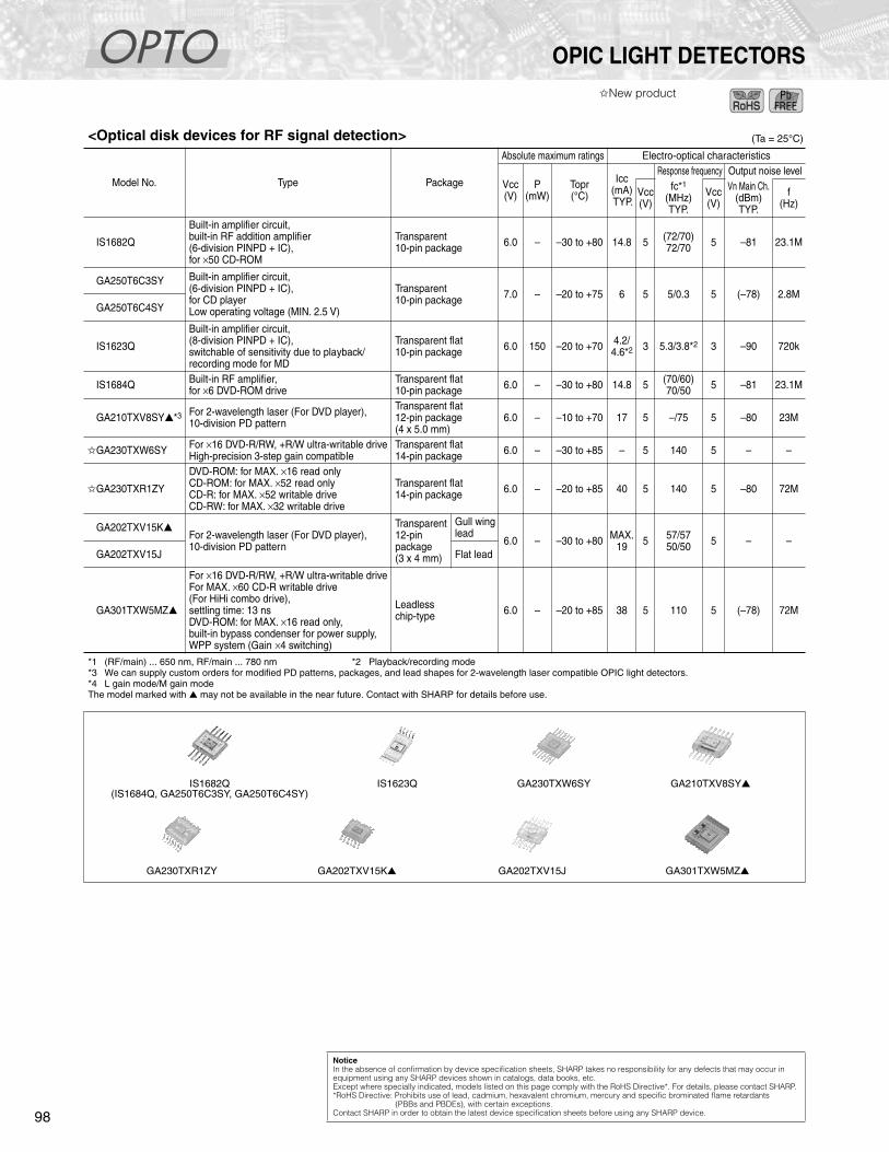
OPTO
98
OPIC LIGHT DETECTORS
New product
<Optical disk devices for RF signal detection>
*1 (RF/main) ... 650 nm, RF/main ... 780 nm *2 Playback/recording mode*3 We can supply custom orders for modified PD patterns, packages, and lead shapes for 2-wavelength laser compatible OPIC light detectors.*4 L gain mode/M gain modeThe model marked with
may not be available in the near future. Contact with SHARP for details before use.
Model No. Type Package
Absolute maximum ratings
Electro-optical characteristics
Vcc (V)
P (mW)
Topr (°C)
Icc(mA) TYP.
Response frequency
Output noise level
Vcc (V)
fc*
1
(MHz) TYP.
Vcc (V)
Vn Main Ch.
(dBm) TYP.
f (Hz)
IS1682Q
Built-in amplifier circuit, built-in RF addition amplifier (6-division PINPD + IC), for
×
50 CD-ROM
Transparent 10-pin package 6.0 – –30 to +80 14.8 5 (72/70)
72/70 5 –81 23.1M
GA250T6C3SY Built-in amplifier circuit, (6-division PINPD + IC), for CD playerLow operating voltage (MIN. 2.5 V)
Transparent 10-pin package 7.0 – –20 to +75 6 5 5/0.3 5 (–78) 2.8M
GA250T6C4SY
IS1623Q
Built-in amplifier circuit, (8-division PINPD + IC), switchable of sensitivity due to playback/recording mode for MD
Transparent flat10-pin package 6.0 150 –20 to +70 4.2/
4.6*
2
3 5.3/3.8*
2
3 –90 720k
IS1684Q Built-in RF amplifier, for
×
6 DVD-ROM driveTransparent flat10-pin package 6.0 – –30 to +80 14.8 5 (70/60)
70/50 5 –81 23.1M
GA210TXV8SY
*
3
For 2-wavelength laser (For DVD player), 10-division PD pattern
Transparent flat12-pin package(4 x 5.0 mm)
6.0 – –10 to +70 17 5 –/75 5 –80 23M
GA230TXW6SY For
×
16 DVD-R/RW, +R/W ultra-writable drive High-precision 3-step gain compatible
Transparent flat14-pin package 6.0 – –30 to +85 – 5 140 5 – –
GA230TXR1ZY
DVD-ROM: for MAX.
×
16 read onlyCD-ROM: for MAX.
×
52 read onlyCD-R: for MAX.
×
52 writable driveCD-RW: for MAX.
×
32 writable drive
Transparent flat14-pin package 6.0 – –20 to +85 40 5 140 5 –80 72M
GA202TXV15K
For 2-wavelength laser (For DVD player), 10-division PD pattern
Transparent 12-pin package (3 x 4 mm)
Gull wing lead
6.0 – –30 to +80 MAX. 19 5 57/57
50/50 5 – –GA202TXV15J Flat lead
GA301TXW5MZ
For
×
16 DVD-R/RW, +R/W ultra-writable drive For MAX.
×
60 CD-R writable drive (For HiHi combo drive), settling time: 13 ns DVD-ROM: for MAX.
×
16 read only, built-in bypass condenser for power supply,WPP system (Gain
×
4 switching)
Leadless chip-type 6.0 – –20 to +85 38 5 110 5 (–78) 72M
IS1682Q(IS1684Q, GA250T6C3SY, GA250T6C4SY)
IS1623Q GA230TXW6SY GA210TXV8SY
GA230TXR1ZY GA202TXV15K
GA202TXV15J GA301TXW5MZ
(Ta = 25°C)
Notice
In the absence of confirmation by device specification sheets, SHARP takes no responsibility for any defects that may occur in equipment using any SHARP devices shown in catalogs, data books, etc. Except where specially indicated, models listed on this page comply with the RoHS Directive*. For details, please contact SHARP.*RoHS Directive: Prohibits use of lead, cadmium, hexavalent chromium, mercury and specific brominated flame retardants (PBBs and PBDEs), with certain exceptions.Contact SHARP in order to obtain the latest device specification sheets before using any SHARP device.

99
Opto
elec
tron
ics
OPIC LIGHT DETECTORS
<Laser power monitoring diode for optical disc system>
*1 Power monitoring photodiodes are also available. Please refer to the page for photodiodes.The model marked with
may not be available in the near future. Contact with SHARP for details before use.
Model No. Type Package
Absolute maximum ratings Electro-optical characteristics
Vcc (V)
P (mW)
Topr (°C)
Icc(mA) TYP.
Response frequency
Vcc (V)
fc(MHz) MIN.
Vcc (V)
GA104T1M1MZ
For
×
48 CD-R writable drive built-in amplifier circuit
Leadless chip-type [3.0 x 3.5 mm] 6.0 – –20 to +70 20 5 50 5
GA104T1M1MZ
(Ta = 25°C)
Notice
In the absence of confirmation by device specification sheets, SHARP takes no responsibility for any defects that may occur in equipment using any SHARP devices shown in catalogs, data books, etc. Except where specially indicated, models listed on this page comply with the RoHS Directive*. For details, please contact SHARP.*RoHS Directive: Prohibits use of lead, cadmium, hexavalent chromium, mercury and specific brominated flame retardants (PBBs and PBDEs), with certain exceptions.Contact SHARP in order to obtain the latest device specification sheets before using any SHARP device.
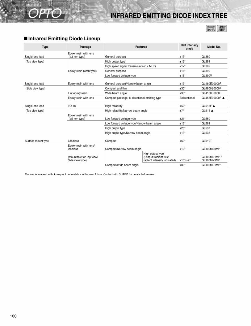
OPTO
100
INFRARED EMITTING DIODE INDEX TREE
Infrared Emitting Diode Lineup
The model marked with
may not be available in the near future. Contact with SHARP for details before use.
Type Package Features Half intensity angle Model No.
Single-end leadEpoxy resin with lens (ø3 mm type) General purpose ±13° GL380
(Top view type) High output type ±13° GL381
High speed signal transmission (12 MHz) ±17° GL382
Epoxy resin (Arch type) General purpose ±18° GL390
Low forward voltage type ±18° GL390V
Single-end lead Epoxy resin with lens General purpose/Narrow beam angle ±13° GL480E00000F
(Side view type) Compact and thin ±30° GL4800E0000F
Flat epoxy resin Wide beam angle ±90° GL4100E0000F
Epoxy resin with lens Compact package, bi-directional emitting type Bidirectional GL453E00000F
Single-end lead TO-18 High reliability ±50° GL513F
(Top view type) High reliability/Narrow beam angle ±7° GL514
Epoxy resin with lens (ø5 mm type) Low forward voltage type ±21° GL560
Low forward voltage type/Narrow beam angle ±13° GL561
High output type ±25° GL537
High output type/Narrow beam angle ±13° GL538
Surface mount type Leadless Compact ±60° GL610T
Epoxy resin with lens/leadless Compact/Narrow beam angle ±10° GL100MN0MP
(Mountable for Top view/Side view type)
High output type (Output: radiant flux/radiant intensity indicated) ±10°/±9°
GL100MN1MP / GL100MN3MP
Compact/Wide beam angle ±80° GL100MD1MP1

101
Opto
elec
tron
ics
INFRARED EMITTING DIODES
Infrared Emitting Diodes
*1 Radiant intensity mW/srNote) Some products are handled by the Compound Semiconductor Division.The model marked with
may not be available in the near future. Contact with SHARP for details before use.
Model No. Package, featuresAbsolute maximum ratings
Φ
e (mW) V
F
(V)
∆θ
(°)
TYP.
λ
p (nm) TYP.
I
F
(mA)
V
R
(V)P
(mW)Topr (°C) MIN. TYP. I
F
(mA) TYP. MAX. I
F
(mA)
GL380ø3 epoxy resin
60 6 150 –25 to +85 4.5*
1
11*
1
50 1.3 1.5 50 ±13 950
GL381 60 6 150 –25 to +85 8.5*
1
20*
1
50 1.3 1.5 50 ±13 950
GL382 ø3 epoxy resin, for high speed signal transmission:12 MHz 60 4 – –25 to +85 6 18 50 1.5 1.7 50 ±17 880
GL390Arch type
60 6 150 –25 to +85 7*
1
13*
1
50 1.3 1.5 50 ±18 950
GL390V 60 6 150 –25 to +85 9*
1
16*
1
50 1.3 1.5 50 ±18 950
GL453E00000F
Resin with bidirectional lens 50 6 75 –25 to +85 0.85 1.3 20 1.2 1.5 20 (Bidirec-tional) 950
GL480E00000FEpoxy resin with lens
50 6 75 –25 to +85 0.7 – 20 1.2 1.4 20 ±13 950
GL4800E0000F 50 6 75 –25 to +85 0.7 1.6 20 1.2 1.4 20 ±30 950
GL4100E0000F Side-view flat type, Epoxy resin 50 6 75 –25 to +85 1.0 – 20 1.2 1.4 20 ±90 950
GL513F
TO-18150 6 250 –40 to +125 1.44 2.88 100 1.35 1.6 100 ±50 950
GL514
150 6 250 –40 to +125 3.31 5.35 100 1.35 1.6 100 ±7 950
GL560
ø5 epoxy resin
100 6 150 –25 to +85 5*
1
14*
1
50 1.25 1.37 50 ±21 940
GL561 100 6 150 –25 to +85 12*
1
25*
1
50 1.25 1.37 50 ±13 940
GL537 100 6 150 –25 to +85 6*
1
13*
1
50 1.3 1.5 50 ±25 950
GL538 100 6 150 –25 to +85 15*
1
30*
1
50 1.3 1.5 50 ±13 950
GL610T Leadless chip type 50 6 150 –25 to +85 0.7 2 20 1.3 1.5 50 ±60 950
GL100MN0MP Surface mounting leadless type, Epoxy resin board with lens 50 6 75 –30 to +85 1.0 3.0
(MAX.) 20 1.2 1.4 20 ±10 940
GL100MN1MPSurface mounting leadless type, Epoxy resin board with lens, high output type
50 6 75 –30 to +85 2.0 6.0(MAX.) 20 1.2 1.5 20 ±10 940
GL100MN3MPSurface mounting leadless type, Epoxy resin board with lens, high output type
50 6 75 –30 to +85 3.0*
1
6.0*
1
20 1.25 1.5 20 ±9 940
GL100MD1MP1Surface mounting leadless type, Epoxy resin board with lens, wide beam angle
50 6 75 –30 to +85 – 6.0(MAX.) 20 – 1.5 20 ±80 940
GL380 (GL381, GL382)
GL390(GL390V)
GL453E00000F
GL480E00000F GL4800E0000F GL4100E0000F
GL513F
GL514
GL560(GL561)
GL537(GL538)
GL610T GL100MN0MPGL100MN1MP, GL100MN3MP,GL100MD1MP1
(Ta = 25°C)
Notice
In the absence of confirmation by device specification sheets, SHARP takes no responsibility for any defects that may occur in equipment using any SHARP devices shown in catalogs, data books, etc. Except where specially indicated, models listed on this page comply with the RoHS Directive*. For details, please contact SHARP.*RoHS Directive: Prohibits use of lead, cadmium, hexavalent chromium, mercury and specific brominated flame retardants (PBBs and PBDEs), with certain exceptions.Contact SHARP in order to obtain the latest device specification sheets before using any SHARP device.
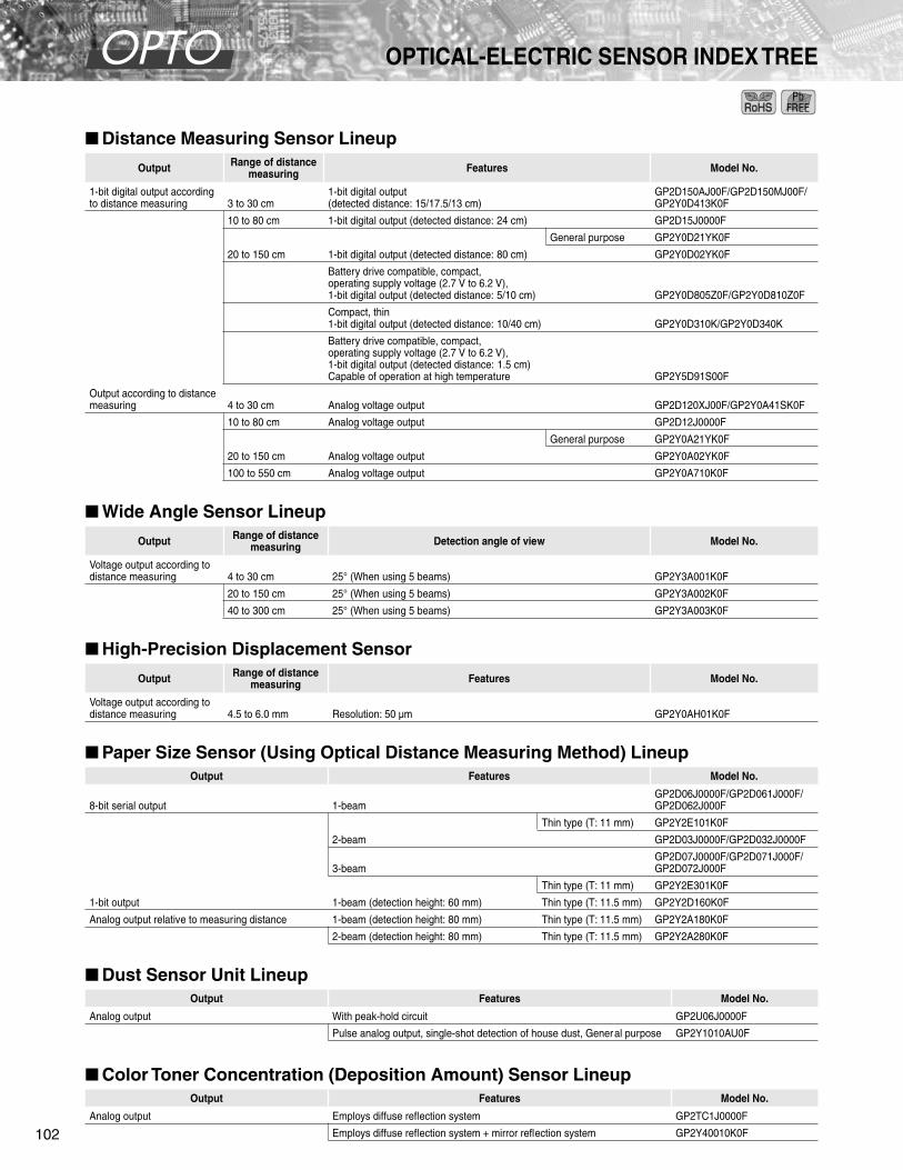
OPTO
102
OPTICAL-ELECTRIC SENSOR INDEX TREE
Distance Measuring Sensor Lineup
Wide Angle Sensor Lineup
High-Precision Displacement Sensor
Paper Size Sensor (Using Optical Distance Measuring Method) Lineup
Dust Sensor Unit Lineup
Output Range of distance measuring Features Model No.
1-bit digital output according to distance measuring 3 to 30 cm
1-bit digital output (detected distance: 15/17.5/13 cm)
GP2D150AJ00F/GP2D150MJ00F/GP2Y0D413K0F
10 to 80 cm 1-bit digital output (detected distance: 24 cm) GP2D15J0000F
General purpose GP2Y0D21YK0F
20 to 150 cm 1-bit digital output (detected distance: 80 cm) GP2Y0D02YK0F
Battery drive compatible, compact, operating supply voltage (2.7 V to 6.2 V), 1-bit digital output (detected distance: 5/10 cm) GP2Y0D805Z0F/GP2Y0D810Z0F
Compact, thin1-bit digital output (detected distance: 10/40 cm) GP2Y0D310K/GP2Y0D340K
Battery drive compatible, compact, operating supply voltage (2.7 V to 6.2 V), 1-bit digital output (detected distance: 1.5 cm)Capable of operation at high temperature GP2Y5D91S00F
Output according to distance measuring 4 to 30 cm Analog voltage output GP2D120XJ00F/GP2Y0A41SK0F
10 to 80 cm Analog voltage output GP2D12J0000F
General purpose GP2Y0A21YK0F
20 to 150 cm Analog voltage output GP2Y0A02YK0F
100 to 550 cm Analog voltage output GP2Y0A710K0F
Output Range of distance measuring Detection angle of view Model No.
Voltage output according to distance measuring 4 to 30 cm 25° (When using 5 beams) GP2Y3A001K0F
20 to 150 cm 25° (When using 5 beams) GP2Y3A002K0F
40 to 300 cm 25° (When using 5 beams) GP2Y3A003K0F
Output Range of distance measuring Features Model No.
Voltage output according to distance measuring 4.5 to 6.0 mm Resolution: 50 µm GP2Y0AH01K0F
Output Features Model No.
8-bit serial output 1-beamGP2D06J0000F/GP2D061J000F/GP2D062J000F
Thin type (T: 11 mm) GP2Y2E101K0F
2-beam GP2D03J0000F/GP2D032J0000F
3-beamGP2D07J0000F/GP2D071J000F/GP2D072J000F
Thin type (T: 11 mm) GP2Y2E301K0F
1-bit output 1-beam (detection height: 60 mm) Thin type (T: 11.5 mm) GP2Y2D160K0F
Analog output relative to measuring distance 1-beam (detection height: 80 mm) Thin type (T: 11.5 mm) GP2Y2A180K0F
2-beam (detection height: 80 mm) Thin type (T: 11.5 mm) GP2Y2A280K0F
Output Features Model No.
Analog output With peak-hold circuit GP2U06J0000F
Pulse analog output, single-shot detection of house dust, General purpose GP2Y1010AU0F
Color Toner Concentration (Deposition Amount) Sensor Lineup
Output Features Model No.
Analog output Employs diffuse reflection system GP2TC1J0000F
Employs diffuse reflection system + mirror reflection system GP2Y40010K0F
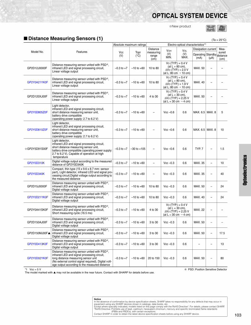
103
Opto
elec
tron
ics
OPTICAL SYSTEM DEVICE
New product
Distance Measuring Sensors (1)
*1 Vcc = 5 V
PSD: Position Sensitive DetectorThe model marked with
may not be available in the near future. Contact with SHARP for details before use.
Model No. Features
Absolute maximum ratings Electro-optical characteristics*
1
Vcc(V)
Topr(°C)
Distance measuring
range (cm)
V
OH
(V)
MIN.
V
OL
(V)
MAX.
Dissipation current Mea-sured
distance(cm)
Operating(mA)
Standby(µA)
GP2D12J0000FDistance measuring sensor united with PSD
, infrared LED and signal processing circuit,Linear voltage output
–0.3 to +7 –10 to +60 10 to 80
V
O
(TYP.) = 0.4 V (at L = 80 cm),
∆
V
O
(TYP.) = 2.0 V(at L: 80 cm
→
10 cm)
MAX. 50 – –
GP2Y0A21YK0FDistance measuring sensor united with PSD
, infrared LED and signal processing circuit,Linear voltage output
–0.3 to +7 –10 to +60 10 to 80
V
O
(TYP.) = 0.4 V (at L = 80 cm),
∆
V
O
(TYP.) = 1.9 V(at L: 80 cm
→
10 cm)
MAX. 40 – –
GP2D120XJ00FDistance measuring sensor united with PSD
, infrared LED and signal processing circuit,Linear voltage output
–0.3 to +7 –10 to +60 4 to 30
V
O
(TYP.) = 0.4 V (at L = 30 cm),
∆
V
O
(TYP.) = 2.25 V(at L = 30 cm
→
4 cm)
MAX. 50 – –
GP2Y0D805Z0F
Light detector, infrared LED and signal processing circuit, short distance measuring sensor unit, battery drive compatible (operating power supply: 2.7 to 6.2 V)
–0.3 to +7 –10 to +60 – Vcc –0.6 0.6 MAX. 6.5 MAX. 8 5
GP2Y0D810Z0F
Light detector, infrared LED and signal processing circuit, short distance measuring sensor unit, battery drive compatible (operating power supply: 2.7 to 6.2 V)
–0.3 to +7 –10 to +60 – Vcc –0.6 0.6 MAX. 6.5 MAX. 8 10
GP2Y5D91S00F
Light detector, infrared LED and signal processing circuit, short distance measuring sensor unit, battery drive compatible (operating power supply: 2.7 to 6.2 V), Capable of operation at high temperature
–0.3 to +7 –30 to +105 – Vcc –0.6 0.6 TYP. 7 – 1.5
GP2Y0D310K Digital voltage output according to the measureddistance of GP2Y0D340K –0.3 to +7 –10 to +60 – Vcc –0.3 0.6 MAX. 35 – 10
GP2Y0D340K
Compact, thin type (15 x 9.6 x 8.7 mm: sensor part), Light detector, infrared LED and signal pro-cessing circuit,Digital voltage output according to the measured distance
–0.3 to +7 –10 to +60 – Vcc –0.3 0.6 MAX. 35 – 40
GP2D15J0000FDistance measuring sensor united with PSD
, infrared LED and signal processing circuit,Digital voltage output
–0.3 to +7 –10 to +60 10 to 80 Vcc –0.3 0.6 MAX. 50 – 24
GP2Y0D21YK0FDistance measuring sensor united with PSD
, infrared LED and signal processing circuit,Digital voltage output
–0.3 to +7 –10 to +60 10 to 80 Vcc –0.3 0.6 MAX. 40 – 24
GP2Y0A41SK0FDistance measuring sensor united with PSD
, infrared LED and signal processing circuit,Short measuring cycle (16.5 ms)
–0.3 to +7 –10 to +60 4 to 30
V
O
(TYP.) = 0.4 V (at L = 30 cm),
∆
V
O
(TYP.) = 2.25 V(at L = 30 cm
→
4 cm)
MAX. 22 – –
GP2D150AJ00FDistance measuring sensor united with PSD
, infrared LED and signal processing circuit,Digital voltage output
–0.3 to +7 –10 to +60 3 to 30 Vcc –0.3 0.6 MAX. 50 – –
GP2D150MJ00F
Distance measuring sensor united with PSD
, infrared LED and signal processing circuit,Digital voltage output
–0.3 to +7 –10 to +60 3 to 30 Vcc –0.3 0.6 MAX. 50 – 17.5
GP2Y0D413K0FDistance measuring sensor united with PSD
, infrared LED and signal processing circuit,Digital voltage output
–0.3 to +7 –10 to +60 3 to 30 Vcc –0.3 0.6 – – 13
GP2Y0D02YK0F
Distance measuring sensor united with PSD
, infrared LED and signal processing circuit, long distance measuring sensor unit (No external control signal required), Digital volt-age output according to the measured distance
–0.3 to +7 –10 to +60 20 to 150 Vcc –0.3 0.6 MAX. 50 – 80
(Ta = 25°C)
Notice
In the absence of confirmation by device specification sheets, SHARP takes no responsibility for any defects that may occur in equipment using any SHARP devices shown in catalogs, data books, etc. Except where specially indicated, models listed on this page comply with the RoHS Directive*. For details, please contact SHARP.*RoHS Directive: Prohibits use of lead, cadmium, hexavalent chromium, mercury and specific brominated flame retardants (PBBs and PBDEs), with certain exceptions.Contact SHARP in order to obtain the latest device specification sheets before using any SHARP device.

OPTO
104
OPTICAL SYSTEM DEVICE
New product
Distance Measuring Sensors (2)
*1 Vcc = 5 V
PSD: Position Sensitive Detector
Wide Angle Sensors
PSD: Position Sensitive Detector L = Reflector - Sensor distanceReflector used: White paper (Gray chart R-27/white surface, made by Kodak Corp., reflectance 90%)
*1 L = 4 cm *4 Change in output voltage from L = 4 cm to 10 cm*2 L = 20 cm *5 Change in output voltage from L = 20 cm to 80 cm*3 L = 40 cm *6 Change in output voltage from L = 40 cm to 100 cm
Model No. Features
Absolute maximum ratings Electro-optical characteristics*
1
Vcc(V)
Topr(°C)
Distance measuring
range (cm)
V
OH
(V)
MIN.
V
OL
(V)
MAX.
Dissipation current Mea-sured
distance(cm)
Operating(mA)
Standby(µA)
GP2Y0A02YK0F Distance measuring sensor united with PSD
, infrared LED and signal processing circuit –0.3 to +7 –10 to +60 20 to 150
V
O
(TYP.) = 0.4 V (at L = 150 cm),
∆
V
O
(TYP.) = 2.0 V(at L = 150 cm
→
20 cm)
MAX. 50 – –
GP2Y0A710K0F Distance measuring sensor united with PSD
, infrared LED and signal processing circuit –0.3 to +7 –10 to +60 100 to 550
V
O
(TYP.) = 2.5 V (at L = 100 cm),
∆
V
O
(TYP.) = 0.7 V(at L = 100 cm
→
200 cm)
TYP. 30 – –
GP2Y5D91S00F GP2Y0D805Z0F(GP2Y0D810Z0F)
GP2Y0D340K(GP2Y0D310K)
GP2D15J0000FGP2D12J0000F, GP2D120XJ00F, GP2D150AJ00F, GP2Y0A21YK0F, GP2Y0D21YK0F, GP2Y0A41SK0FGP2D150MJ00F, GP2Y0D413K:without mounting hole
GP2Y0D02YK0F(GP2Y0A02YK0F)
GP2Y0A710K0F
Model No. Features
Absolute maximum ratings Electro-optical characteristics
Vcc(V)
Topr(°C)
Distance measuring
range (cm)
Output terminal voltage
(V)
Output voltage
difference (V)
Input voltage (V)
V
IN
H LEDL
GP2Y3A001K0F Distance measuring sensor united with PSD
, infrared LED and signal processing circuit,Distance measuring sensor application product,Wide range (field of view) detection using 5 infrared beams
–0.3 to +7 –10 to +60 4 to 30 TYP. 2.8*
1
TYP. 1.6*
4
MIN. 4.5 MAX. 0.5
GP2Y3A002K0F –0.3 to +7 –10 to +60 20 to 150 TYP. 2.3*
2
TYP. 1.6*
5
MIN. 4.5 MAX. 0.5
GP2Y3A003K0F –0.3 to +7 –10 to +60 40 to 300 TYP. 2.2*
3
TYP. 1.2*
6
MIN. 4.5 MAX. 0.5
GP2Y3A001K0F GP2Y3A002K0F GP2Y3A003K0F
(Ta = 25°C)
(Ta = 25°C)
Notice
In the absence of confirmation by device specification sheets, SHARP takes no responsibility for any defects that may occur in equipment using any SHARP devices shown in catalogs, data books, etc. Except where specially indicated, models listed on this page comply with the RoHS Directive*. For details, please contact SHARP.*RoHS Directive: Prohibits use of lead, cadmium, hexavalent chromium, mercury and specific brominated flame retardants (PBBs and PBDEs), with certain exceptions.Contact SHARP in order to obtain the latest device specification sheets before using any SHARP device.
!

105
Opto
elec
tron
ics
OPTICAL SYSTEM DEVICE
Paper Size Sensors
This table shows the characteristics when configured in the paper size sensor system.*1 Reflectivity: 18% or more, OD = log (1/T), T: Reflectivity*2 Paper detection height GP2D061: TYP. 45 mm GP2D062: TYP. 90 mm*3 Paper detection height GP2D071: TYP. 45 mm*4 Paper detection height GP2D032: TYP. 45 mm
Model No. Features
Operating temperature
Supply voltage
Paper detection
height
LED beam pitch
Approved value of paper
position sliding
Paper detection
density
Dissipation current
Topr (°C)
Vcc (V)
H (mm)
Lp (mm)
∆
x (mm) OD Icc
(mA)GP2D03J0000FGP2D032J0000F*
4
8-bit serial output using optical distance measuring method (2-beam) 0 to +60 5 ±0.5 TYP. 60 TYP. 21 MAX. ±6 0.7 or less*
1
TYP. 30
GP2D06J0000FGP2D061J000F*
2
GP2D062J000F*
2
8-bit serial output using optical distance measuring method (1-beam) 0 to +60 5 ±0.5 TYP. 60 – MAX. ±6 0.7 or less*
1
TYP. 33
GP2Y2E101K0FThin type (T: 11 mm)8-bit serial output using optical distance measuring method (1-beam)
0 to +60 5 ±0.5 TYP. 85 – MAX. ±6 0.7 or less*
1
–
GP2Y2D160K0F
Thin type (T: 11.5 mm)using optical distance measuring method (1-beam)Digital output (1-bit)
–10 to +60 5 ±0.5 TYP. 60 – MIN. ±7.5 0.7 or less*
1
–
GP2D07J0000FGP2D071J000F*
3
8-bit serial output using optical distance measuring method (3-beam) 0 to +60 5 ±0.5 TYP. 60 TYP. 36 MAX. ±6 0.7 or less*
1
TYP. 33
GP2Y2E301K0FThin type (T: 11 mm)8-bit serial output using optical distance measuring method (3-beam)
0 to +60 5 ±0.5 TYP. 85 TYP. 33 MAX. ±6 0.7 or less*
1
–
GP2Y2A180K0FThin type (T: 11.5 mm)Analog output using optical distance measuring method (1-beam)
–10 to +60 5 ±0.5 TYP. 80 – – – MAX. 25
GP2Y2A280K0FThin type (T: 11.5 mm)Analog output using optical distance measuring method (2-beam)
–10 to +60 5 ±0.5 TYP. 80 – – – MAX. 50
GP2D03J0000F(GP2D032J000F)
GP2D06J0000F(GP2D061J000F/GP2D062J000F)
GP2Y2E101K0F GP2Y2D160K0F GP2Y2A180K0F
GP2D07J0000F(GP2D071J000F)
GP2Y2E301K0F GP2Y2A280K0F
(Ta = 25°C)
Notice
In the absence of confirmation by device specification sheets, SHARP takes no responsibility for any defects that may occur in equipment using any SHARP devices shown in catalogs, data books, etc. Except where specially indicated, models listed on this page comply with the RoHS Directive*. For details, please contact SHARP.*RoHS Directive: Prohibits use of lead, cadmium, hexavalent chromium, mercury and specific brominated flame retardants (PBBs and PBDEs), with certain exceptions.Contact SHARP in order to obtain the latest device specification sheets before using any SHARP device.
"

OPTO
106
OPTICAL SYSTEM DEVICE
New product
High-Precision Displacement Sensor
Dust Sensor Units
The model marked with
may not be available in the near future. Contact with SHARP for details before use.
Color Toner Concentration (Deposition Amount) Sensors
*1 Dissipation current with LED drive current of I
F
= 0 mA*2 With reflection object A (Reflectance: 15.6%)
Model No. Features Topr (°C)
Operating supply voltage
(V)
Dissipation current (mA)
Distance measuring range (mm)
Distance characteristic of output
GP2Y0AH01K0F Resolution: 50 µm –10 to +60 4.5 to 5.5 TYP. 20 4.5 to 6.0TYP. 1.73 V
Variation in output over range (4.5 to 6.0 mm)
GP2Y0AH01K0F
Model No. Features Topr (°C)
Electro-optical characteristicsOperating
supply voltage (V)
Dissipation current (mA)
Detection sensitivity
V/(0.1 mg/m
3
)
Output voltage at no dust
Voc (V)
Output voltage range
V
OH
(V)
GP2U06J0000F
Built-in infrared emitting diode, photodiode and signal processing circuit –10 to +65 4.5 to 5.5 TYP. 15 TYP. 0.5 MAX. 1 MIN. 3.2
GP2Y1010AU0F Compact, single-shot detection of house dust –10 to +65 4.5 to 5.5 TYP. 11 TYP. 0.5 TYP. 0.9 MIN. 3.4
GP2U06J0000F GP2Y1010AU0F
Model No. Features Topr (°C)
Electro-optical characteristicsDissipation current
(mA)Output voltage
V
01
(V)Output voltage
V
02
(V)
GP2TC1J0000F Employs diffuse reflection system, high-precision detection of toner concentration on photo-sensitive drum, 2-line analog output 0 to +60 TYP. 4*
1
TYP. 1.06*
2
TYP. 2.63*
2
GP2Y40010K0FEmploys diffuse reflection system + mirror reflection system, high-precision detection of toner concentration on transfer belt, 2-line analog output
0 to +60 MAX. 10 MAX. 1.61 MAX. 3.5
GP2TC1J0000F GP2Y40010K0F
(Ta = 25°C)
(Ta = 25°C)
(Ta = 25°C)
Notice
In the absence of confirmation by device specification sheets, SHARP takes no responsibility for any defects that may occur in equipment using any SHARP devices shown in catalogs, data books, etc. Except where specially indicated, models listed on this page comply with the RoHS Directive*. For details, please contact SHARP.*RoHS Directive: Prohibits use of lead, cadmium, hexavalent chromium, mercury and specific brominated flame retardants (PBBs and PBDEs), with certain exceptions.Contact SHARP in order to obtain the latest device specification sheets before using any SHARP device.
#
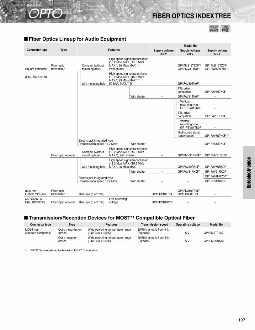
OPTO
107
Opto
elec
tron
ics
FIBER OPTICS INDEX TREE
Fiber Optics Lineup for Audio Equipment
Transmission/Reception Devices for MOST*
1
Compatible Optical Fiber
*1 “MOST” is a registered trademark of MOST Cooperation.
Connector type Type FeaturesModel No.
Supply voltage 2.5 V
Supply voltage 3.0 V
Supply voltage 5.0 V
Square connectorFiber optic transmitter
Compact (without mounting hole)
High speed signal transmission (13.2 Mb/s MAX., 15.5 Mb/s MAX.*, 50 Mb/s MAX.**), With shutter –
GP1FM313TZ0F*/GP1FMV31TK0F*
GP1FM513TZ0F/GP1FM55HTZ0F**
(EIAJ RC-5720B)
with mounting hole
High speed signal transmission (13.2 Mb/s MAX. [15.5 Mb/s MAX.*, 25 Mb/s MAX.**, 50 Mb/s MAX.***]) – GP1FAV30TK0F* –
TTL drive compatible GP1FAV50TK0F
With shutter – GP1FAV31TK0F* –
Vertical mounting typeGP1FSV31TK0F –
TTL drive compatible GP1FAV51TK0F
Vertical mounting typeGP1FSV51TK0F –
High speed signal transmission GP1FAV55TK0F***
Electric jack integrated type(Transmission speed 13.2 Mb/s) With shutter – – GP1FP513TK0F
Fiber optic receiverCompact (without mounting hole)
High speed signal transmission (13.2 Mb/s MAX., 15.5 Mb/s MAX.*), With shutter – GP1FMV31RK0F* GP1FMV51RK0F
with mounting hole
High speed signal transmission (13.2 Mb/s MAX. [15.5 Mb/s MAX.*, 25 Mb/s MAX.**]) – GP1FAV30RK0F* GP1FAV50RK0F
With shutter – GP1FAV31RK0F* GP1FAV51RK0F
Electric jack integrated type(Transmission speed 13.2 Mb/s)
GP1FA51HRZ0F**
With shutter – – GP1FP513RK0F
ø3.5 mm Optical mini-jack
Fiber optic transmitter Thin type (t: 4.2 mm) GP1FD210TP0F
GP1FD310TP0F/GP1FD320TP0F –
(JIS C6560 &EIAJ RC5720B) Fiber optic receiver Thin type (t: 4.2 mm)
Low operating voltage GP1FD210RP0F – –
Connector type Type Features Transmission speed Operating voltage Model No.
MOST ver1.1 standard compatible
Optic transmission device
Wide operating temperature range (–40°C to +105°C)
25Mb/s as optic fiber link (Biphase) 5 V GP5FM5T01AZ
Optic reception device
Wide operating temperature range (–40°C to +105°C)
25Mb/s as optic fiber link (Biphase) 5 V GP5FM5R01AZ

OPTO
108
FIBER OPTICS
New product
Fiber Optic Transmitters (Square Connector)
Fiber Optic Transmitters (ø3.5 mm Optical Mini-jack)
Model No. Features
Absolute maximum ratings Electro-optical characteristics
Vcc (V)
Vin (V)
Topr(°C)
Supply voltage
(V)
Propagation delay time
Dissipation current
Icc (mA)MAX.
Pulse width
distortion
∆
tw(ns)
Transmis-sion speed
T (Mb/s) MAX.
t
PLH
(ns) MAX.
t
PHL
(ns) MAX.
GP1FM313TZ0FCompact (without mounting hole), With shutter, High response speed (up to x2)
–0.5 to +7 –0.5 to Vcc + 0.5 –20 to +70 2.7 to 3.6 180 180 12 ±15 15.5
GP1FMV31TK0FCompact (without mounting hole), With shutter, High response speed (up to x2)
–0.5 to +7 –0.5 to Vcc + 0.5 –20 to +70 2.7 to 5.25 180 180 12 ±15 15.5
GP1FM513TZ0FCompact (without mounting hole), With shutter, High response speed (up to x2)
–0.5 to +7 –0.5 to Vcc + 0.5 –20 to +70 4.75 to 5.25 180 180 13 ±15 13.2
GP1FMV51TK0FCompact (without mounting hole), With shutter, High response speed (up to x2)
–0.5 to +7 –0.5 to Vcc + 0.5 –20 to +70 4.75 to 5.25 180 180 13 ±15 13.2
GP1FM55HTZ0FCompact (without mounting hole), With shutter, High response speed (up to x2)
–0.5 to +7 –0.5 to Vcc + 0.5 –20 to +70 4.75 to 5.25 180 180 13 ±15 50
GP1FAV30TK0FWith mounting hole, Low voltage drive, High response speed (up to x2)
–0.5 to +7 –0.5 to Vcc + 0.5 –20 to +70 2.7 to 5.25 180 180 12 ±15 15.5
GP1FAV50TK0F
With mounting hole, Mass-market model, High response speed (up to x2),TTL drive compatible
–0.5 to +7 –0.5 to Vcc + 0.5 –20 to +704.75 to 5.25
Input voltage: MIN. 2.0 V
180 180 13 ±15 13.2
GP1FAV51TK0F
With mounting hole, Mass-market model, High response speed, With shutter, TTL drive compatible
–0.5 to +7 –0.5 to Vcc + 0.5 –20 to +70 4.75 to 5.25 180 180 13 ±15 13.2
GP1FSV51TK0F
With mounting hole, Vertical mounting, With shutter, Low voltage drive, High response speed
–0.5 to +7 –0.5 to Vcc + 0.5 –20 to +70 4.75 to 5.25 180 180 13 ±15 13.2
GP1FAV31TK0FWith mounting hole, With shutter, Low voltage drive, High response speed
–0.5 to +7 –0.5 to Vcc + 0.5 –20 to +70 2.7 to 5.25 180 180 12 ±15 15.5
GP1FSV31TK0F
With mounting hole, Vertical mounting, With shutter, Low voltage drive, High response speed
–0.5 to +7 –0.5 to Vcc + 0.5 –20 to +70 2.7 to 5.25 180 180 13 ±15 15.5
GP1FAV55TK0FWith mounting hole, High response speed (50 Mb/s), With shutter
–0.5 to +7 –0.5 to Vcc + 0.5 –20 to +70 4.75 to 5.25 180 180 13 ±15 50
GP1FP513TK0F Electric jack/optical connector integrated type –0.5 to +7 –0.5 to Vcc + 0.5 –20 to +70 4.75 to 5.25 180 180 13 ±15 13.2
Model No. Features
Absolute maximum ratings Electro-optical characteristics
Vcc (V)
Vin (V)
Topr(°C)
Supply voltage
(V)
Propagation delay time
Dissipation current
Icc (mA)MAX.
Pulse width
distortion
∆
tw(ns)
Transmis-sion speed
T (Mb/s) MAX.
t
PLH
(ns) MAX.
t
PHL
(ns) MAX.
GP1FD210TP0F Compact, Thin type (t: 4.2 mm), Optical mini-jack (low voltage type) –0.5 to +7 –0.5 to Vcc + 0.5 –20 to +70 2.2 to 3.0 180 180 10 ±30 8
GP1FD310TP0F Compact, Thin type (t: 4.2 mm), Optical mini-jack (low voltage type) –0.5 to +7 –0.5 to Vcc + 0.5 –20 to +70 2.7 to 3.6 180 180 12 ±30 8
GP1FD320TP0F Compact, Thin type (t: 4.2 mm), Optical mini-jack (low voltage type) – – –20 to +70 2.3 to 5.5 – – 12 – 25
(Ta = 25°C)
(Ta = 25°C)
Notice
In the absence of confirmation by device specification sheets, SHARP takes no responsibility for any defects that may occur in equipment using any SHARP devices shown in catalogs, data books, etc. Except where specially indicated, models listed on this page comply with the RoHS Directive*. For details, please contact SHARP.*RoHS Directive: Prohibits use of lead, cadmium, hexavalent chromium, mercury and specific brominated flame retardants (PBBs and PBDEs), with certain exceptions.Contact SHARP in order to obtain the latest device specification sheets before using any SHARP device.

109
Opto
elec
tron
ics
FIBER OPTICS
Fiber Optic Receivers (Square Connector)
Fiber Optic Receivers (ø3.5 mm Optical Mini-jack)
Model No. Features
Absolute maximum ratings Electro-optical characteristics
Vcc (V) I
OL
(mA)
Topr(°C)
Supply voltage
(V)
Propagation delay time
Dissipation current
Icc (mA)MAX.
Pulse width
distortion
∆
tw(ns)
Transmis-sion speed
T (Mb/s) MAX.
t
PLH
(ns) MAX.
t
PHL
(ns) MAX.
GP1FMV31RK0F Compact (without mounting hole), With shutter, High response speed (up to x2) –0.5 to +7 10 –20 to +70 2.7 to 3.6 180 180 15 ±20 15.5
GP1FMV51RK0F Compact (without mounting hole), With shutter, High response speed (up to x2) –0.5 to +7 10 –20 to +70 4.75 to 5.25 180 180 25 ±20 13.2
GP1FAV30RK0F With mounting hole, Low voltage drive, High response speed –0.5 to +7 10 –20 to +70 2.7 to 3.6 180 180 15 ±20 15.5
GP1FAV50RK0F With mounting hole, Mass-market model, High response speed (up to x2) –0.5 to +7 10 –20 to +70 4.75 to 5.25 180 180 25 ±20 13.2
GP1FAV51RK0F High response speed (up to x2), with shutter –0.5 to +7 10 –20 to +70 4.75 to 5.25 180 180 25 ±20 13.2
GP1FAV31RK0F With mounting hole, With shutter, Low voltage drive, High response speed (up to x2) – – –20 to +70 2.7 to 3.6 – – 15 – 15.5
GP1FA51HRZ0F With mounting hole, High response speed (up to x4), with shutter – – –20 to +70 4.75 to 5.25 – – 15 – 25
GP1FP513RK0F Electric jack/optical connector integrated type –0.5 to +7 10 –20 to +70 4.75 to 5.25 180 180 25 ±20 13.2
Model No. Jack Features
Absolute maximum ratings Electro-optical characteristics
Vcc (V) I
OL
(mA)
Topr(°C)
Supply voltage
(V)
Propagation delay time
Dissipation current
Icc (mA)MAX.
Pulse width
distortion
∆
tw(ns)
Transmis-sion speed
T (Mb/s) MAX.
t
PLH
(ns) MAX.
t
PHL
(ns) MAX.
GP1FD210RP0F ø3.5 Thin (thickness: 4.2 mm), optical mini-jack (low voltage drive) –0.5 to +7 4 –20 to +70 2.4 to 3.0 180 180 7.5 ±30 8
GP1FM313 series(GP1FM513 series)
GP1FMV31 series(GP1FMV51 series)
GP1FAV50TK0FGP1FAV50RK0F, GP1FAV30TK0F,GP1FAV30RK0F
GP1FSV31TK0F(GP1FSV51TK0F)
GP1FAV51TK0FGP1FAV31TK0F,GP1FAV55TK0F,GP1FAV51RK0F,GP1FAV31RK0F
GP1FP513TK0F(GP1FP513RK0F)
GP1FD210TP0FGP1FD210RP0F, GP1FD310TP0F,GP1FD320TP0F
(Ta = 25°C)
(Ta = 25°C)
Notice
In the absence of confirmation by device specification sheets, SHARP takes no responsibility for any defects that may occur in equipment using any SHARP devices shown in catalogs, data books, etc. Except where specially indicated, models listed on this page comply with the RoHS Directive*. For details, please contact SHARP.*RoHS Directive: Prohibits use of lead, cadmium, hexavalent chromium, mercury and specific brominated flame retardants (PBBs and PBDEs), with certain exceptions.Contact SHARP in order to obtain the latest device specification sheets before using any SHARP device.
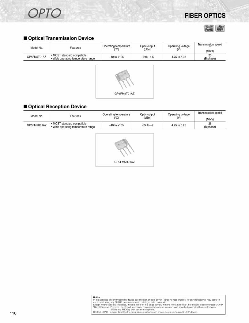
OPTO
110
FIBER OPTICS
Optical Transmission Device
Optical Reception Device
Model No. Features Operating temperature (°C)
Optic output (dBm)
Operating voltage (V)
Transmission speedT
(Mb/s)
GP5FM5T01AZ • MOST standard compatible• Wide operating temperature range –40 to +105 –9 to –1.5 4.75 to 5.25 25
(Biphase)
GP5FM5T01AZ
Model No. Features Operating temperature (°C)
Optic output (dBm)
Operating voltage (V)
Transmission speedT
(Mb/s)
GP5FM5R01AZ • MOST standard compatible• Wide operating temperature range –40 to +105 –24 to –2 4.75 to 5.25 25
(Biphase)
GP5FM5R01AZ
Notice
In the absence of confirmation by device specification sheets, SHARP takes no responsibility for any defects that may occur in equipment using any SHARP devices shown in catalogs, data books, etc. Except where specially indicated, models listed on this page comply with the RoHS Directive*. For details, please contact SHARP.*RoHS Directive: Prohibits use of lead, cadmium, hexavalent chromium, mercury and specific brominated flame retardants (PBBs and PBDEs), with certain exceptions.Contact SHARP in order to obtain the latest device specification sheets before using any SHARP device.

LED
111
LED
HIGH-LUMINOSITY LED LAMPS
High-Luminosity (AIGaInP) LED Series
High-Luminosity (InGaN) LED Series
White Type LED Series
Pastel Color LED Series
LED Series
* C is the opposite polarity of EG’s.
High-Luminosity (AlGaInP) LED Lamps
Taped model is also available.
Radiation color Green Yellow-green Amber Sunset orange Orange Red
Series ZG, JG ZE, JE ZV, JV, YV ZS, JS, YS ZJ, JJ, YJ ZR, JR JU
Dominant emission wavelength (nm) (560) (572) (588) (605) (618) (630) (638)
Radiation material AlGaInP on GaAs
Radiation color Blue Green Radiation color White
Series BC GC Series BW
Dominant emission wavelength (nm) (470) (525) Color range
(x, y) (0.31, 0.31)
Radiation material InGaN Radiation material InGaN + Fluorescent powder
Radiation color Light blue Lemon yellow Purple
Series CA CY CV
Color range (x, y) (0.17, 0.20) (0.42, 0.48) (0.35, 0.15)
Radiation material InGaN + Fluorescent powder
Radiation color Green Yellow-greenYellow-green
(High-luminosity)
Yellow Sunset orange Red Red
Red(High-
luminosity)
Red(High-
luminosity)Red
Series KG, K EG, E, C* FG, F HY, H HS, S HD, D HA, A TR, T UR, U PR, P
Peak emission wavelength (nm) 555 565 565 585 610 635 650 660 660 695
Radiation material GaP GaP GaP GaAsP on
GaPGaAsP on
GaPGaAsP on
GaPGaAsP on
GaP
GaAlAs on GaAs
Single hetero
GaAlAs on GaAlAs
Double heteroGaP
App
eara
nce
Radiation shape
(mm)
Resin typeHigh-luminosity
JG, ZG (Green)
JE, ZE (Yellow-green)
JV, ZV (Amber)
JS, ZS (Sunset orange)
ZJ, JJ (Orange)
ZR, JR, JU (Red)
Col
ored
diff
usio
n
Colo
red
trans
pare
ncy
Colo
rless
tran
spar
ency
Milk
y di
ffusi
on
Model No.
Lum
inou
s in
tens
ity
(mcd
) TY
P. Model No.
Lum
inou
s in
tens
ity
(mcd
) TY
P. Model No.
Lum
inou
s in
tens
ity
(mcd
) TY
P. Model No.
Lum
inou
s in
tens
ity
(mcd
) TY
P. Model No.
Lum
inou
s in
tens
ity
(mcd
) TY
P. Model No.Lu
min
ous
inte
nsity
(m
cd) T
YP.
Cyl
inde
r
ø3
GL3ZV402B0SE
400
GL3ZS402B0SE
400
GL3ZJ402B0SE
400
GL3ZR402B0SE 250
GL3JG402B0SE
85
GL3JE402B0SE
200
GL3JR402B0S3 200
GL3ZV802B0SE
200
GL3ZS802B0SE
210
GL3ZJ802B0SE
230
GL3ZR802B0SE 150
GL3JV404B0SE
280
GL3JS404B0SE
280
GL3JJ404B0SE
200
GL3JV804B0SE
110
GL3JS804B0SE
120
GL3JJ804B0SE
100
ø5
GL5ZV152B0SE
2 700
GL5ZS152B0SE
3 000
GL5ZJ152B0SE
3 000
GL5ZR152B0SE 2 000
GL5ZV302B0SE
900
GL5ZS302B0SE
1 000
GL5ZJ302B0SE
900
GL5ZR302B0SE 600
GL5JV302B0SE
640
GL5JS302B0SE
680
GL5JJ302B0SE
570
ø10
GL0ZV042B0S
16 900
GL0ZS042B0S
22 600
GL0ZJ042B0S
18 500
Ova
l
Long: 5.8Short: 4.6
GL6ZV27
750
GL6ZS27
850
GL6ZJ27
750
GL6ZR27 360
GL5JV7D2D0SE
210
GL5JS7D2D0SE
230
GL5JJ7D2D0SE
190
(Ta = 25°C)
(Ta = 25°C) (Ta = 25°C)
(Ta = 25°C)
(Ta = 25°C)
(IF = 20 mA, Ta = 25°C)
Notice
In the absence of confirmation by device specification sheets, SHARP takes no responsibility for any defects that may occur in equipment using any SHARP devices shown in catalogs, data books, etc.Except where specially indicated, models listed on this page comply with the RoHS Directive*. For details, please contact SHARP.*RoHS Directive: Prohibits use of lead, cadmium, hexavalent chromium, mercury and specific brominated flame retardants (PBBs and PBDEs), with certain exceptions.Contact SHARP in order to obtain the latest device specification sheets before using any SHARP device.

LED
112
HIGH-LUMINOSITY LED LAMPS
New product
High-Luminosity LED Lamps
*1 With tie-bar Taped model is also available.
Appear-ance
Radiation shape(mm)
Resin typeHigh-luminosity
BC (Blue) GC (Green) TR, T (Red) UR, U (Red)C
olor
ed
diffu
sion
Col
ored
tra
nspa
renc
yC
olor
less
tra
nspa
renc
y
Milk
y di
ffusi
on
Model No.
Lum
inou
s in
tens
ity
(mcd
) TY
P. Model No.
Lum
inou
s in
tens
ity
(mcd
) TY
P. Model No.
Lum
inou
s in
tens
ity
(mcd
) TY
P. Model No.
Lum
inou
s in
tens
ity
(mcd
) TY
P.
Cylinder
ø3
GL3TR8 60 GL3UR8 300
GL3TR44 110 GL3UR44 250
GL3TR43 20 GL3UR43 100
GL3BC302B0S2 900
GL3UR402B0S 350
GL3B2402B0SC 650 GL3G2402B0SC 2 800
ø5
GL5TR8 80
GL5UR44 850
GL5UR2K 2 000
GL5UR3K 3 000
GL5TR43 500 GL5UR2K1 2 000
GL5UR3K1 3 000
GL6UR11T*
1
300
GL6UR31 950
Oval Long: 5.8Short: 4.6
GL6UR26T*
1
400
Rectangle
2.0
×
5.0
GL8TR21 4 GL8UR21 16
1.8
×
3.9
GL8TR42 4
GL3UR8 GL3UR43 GL3MM402B0SM series GL3ZS802B0S series GL3JV404B0SE series
GL5UR2KGL5UR3K
GL5UR2K1GL5UR3K1
GL5ZR302B0SE seriesGL5JV302B0SE series
GL6UR11T GL6UR26T
GL6ZR27 seriesGL5JV7D2D0SE series
GL6UR31 GL0ZV042B0S series GL8TR21
(IF = 20 mA, Ta = 25°C)
Notice
In the absence of confirmation by device specification sheets, SHARP takes no responsibility for any defects that may occur in equipment using any SHARP devices shown in catalogs, data books, etc.Except where specially indicated, models listed on this page comply with the RoHS Directive*. For details, please contact SHARP.*RoHS Directive: Prohibits use of lead, cadmium, hexavalent chromium, mercury and specific brominated flame retardants (PBBs and PBDEs), with certain exceptions.Contact SHARP in order to obtain the latest device specification sheets before using any SHARP device.

113
LED
LED LAMPS
LED Lamps
*1 PR series (Red): I
F
= 5 mA (GL8PR25, GL8PR29: I
F
= 10 mA) Taped model is also available.*2 Taped model*3 With tie-barHL: High-luminosity
App
eara
nce
Radiation shape
(mm)
Resin type
Green Yellow-green Yellow-green (HL) Yellow Sunset orange Red Red
Col
ored
diff
usio
n
Col
ored
tran
spar
ency
Col
orle
ss tr
ansp
aren
cy
Milk
y di
ffusi
on
(555 nm)
Lum
inou
s in
tens
ity
(mcd
) TY
P. (565 nm)
Lum
inou
s in
tens
ity
(mcd
) TY
P. (565 nm)
Lum
inou
s in
tens
ity
(mcd
) TY
P. (585 nm)
Lum
inou
s in
tens
ity
(mcd
) TY
P. (610 nm)
Lum
inou
s in
tens
ity
(mcd
) TY
P. (635 nm)
Lum
inou
s in
tens
ity
(mcd
) TY
P. (695 nm)
Lum
inou
s in
tens
ity
(mcd
) TY
P.
Cyl
inde
r
ø3
GL3KG8 30 GL3EG8 60 GL3HY8 55 GL3HS8 60 GL3HD8 40 GL3PR8 8
GL3EG41 130
GL3KG44 60 GL3EG44 130 GL3HY44 100 GL3HS44 100 GL3HD44 110 GL3PR44 12
GL3KG43 20 GL3EG43 38 GL3HY43 25 GL3HS43 25 GL3HD43 25 GL3PR43 3
GL3KG62 22 GL3EG62 65 GL3HY62 40 GL3HS62 40 GL3HD62 50
GL3KG63 6 GL3EG63 18 GL3HY63 16 GL3HS63 15 GL3HD63 17 GL3PR63 2
LT3E31W*
2
18 LT3H31W*
2
15 LT3D31W*
2
15 LT3P31W*
2
1.5
LT3E65W*
2
25 LT3H65W*
2
25 LT3S65W*
2
25 LT3D65W*
2
25 LT3P65W*
2
3
ø4
GL4KG8 30 GL4EG8 100 GL4HY8 110 GL4HS8 80 GL4HD8 110 GL4PR8 15
ø5
GL5EG4 20 GL5HD4 25 GL5PR4 3
GL5KG8 60 GL5EG8 150 GL5HY8 120 GL5HS8 80 GL5HD8 80 GL5PR8 15
GL5KG41 70 GL5EG41 160 GL5HY41 100 GL5HS41 100 GL5HD41 150 GL5PR41 15
GL5KG44 70 GL5EG44 160 GL5HY44 100 GL5HS44 100 GL5HD44 100 GL5PR44 15
GL5EG261B0SB
150
GL5HD261B0SB
80
GL5PR261B0SB
15
GL5EG40 250 GL5HY40 250 GL5HS40 200 GL5HD40 250 GL5PR40 35
GL5KG43 120 GL5EG43 300 GL5FG43 600 GL5HY43 250 GL5HS43 250 GL5HD43 300
GL5EG60 23 GL5HD60 8
GL6EG11T*
3
120
ø5 (Inverted
cone)
GL5EG47 15 GL5HS47 6 GL5HD47 8
Oval
Long: 5.8Short: 4.6
GL6EG26T
*3
140
Convex
ø2
GL2EG6 15 GL2HY6 12 GL2HD6 12 GL2PR6 1.5
Arch2.5
×
5.0
GL8EG2 30 GL8HD2 30
2.0
×
3.1
GL8EG4 50 GL8HD4 40
Rec
tang
le
1.8
×
3.9
GL8KG42 1.5 GL8EG42 5 GL8HY42 6 GL8HD42 5 GL8PR42 0.7
1.9
×
3.9
GL8EG5 28 GL8HY5 25 GL8HD5 22
2.0
×
3.2
GL8KG25 9 GL8EG25 12 GL8HY25 12 GL8HS25 10 GL8HD25 12 GL8PR25 1.5
2.0
×
3.2
GL8KG29 5 GL8EG29 12 GL8HY29 10 GL8HS29 7 GL8PR29 3
2.0
×
4.5
GL8EG23 6 GL8HY23 8 GL8HD23 6
2.0
×
5.0
GL8KG21 4 GL8EG21 8 GL8HY21 8 GL8HS21 8 GL8HD21 8 GL8PR21 0.7
GL8KG26 4 GL8EG26 8 GL8HY26 8 GL8HD26 8 GL8PR26 0.7
Square 5.0
×
5.0
GL8KG22 3.5 GL8EG22 6 GL8HY22 5 GL8HS22 5 GL8HD22 8 GL8PR22 1.2
Triangle Isoscelestriangle
GL8PR28 0.9
(I F = 20 mA*1, Ta = 25°C)
K G E G F G H Y H S H D P R
Notice
In the absence of confirmation by device specification sheets, SHARP takes no responsibility for any defects that may occur in equipment using any SHARP devices shown in catalogs, data books, etc.Except where specially indicated, models listed on this page comply with the RoHS Directive*. For details, please contact SHARP.*RoHS Directive: Prohibits use of lead, cadmium, hexavalent chromium, mercury and specific brominated flame retardants (PBBs and PBDEs), with certain exceptions.Contact SHARP in order to obtain the latest device specification sheets before using any SHARP device.
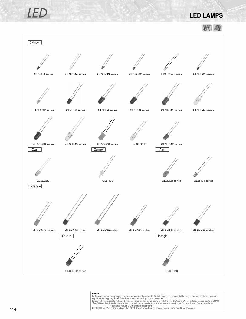
LED
114
LED LAMPS
Cylinder
GL3PR8 series GL3PR44 series GL3HY43 series GL3KG62 series LT3E31W series GL3PR63 series
LT3E65W series GL4PR8 series GL5PR4 series GL5HS8 series GL5KG41 series GL5PR44 series
GL5EG40 series GL5HY43 series GL5EG60 series GL6EG11T GL5HD47 series
Oval Convex Arch
GL6EG26T GL2HY6 GL8EG2 series GL8HD4 series
Rectangle
GL8KG42 series GL8KG25 series GL8HY29 series GL8HD23 series GL8HS21 series GL8HY26 series
Square Triangle
GL8HD22 series GL8PR28
Notice
In the absence of confirmation by device specification sheets, SHARP takes no responsibility for any defects that may occur in equipment using any SHARP devices shown in catalogs, data books, etc.Except where specially indicated, models listed on this page comply with the RoHS Directive*. For details, please contact SHARP.*RoHS Directive: Prohibits use of lead, cadmium, hexavalent chromium, mercury and specific brominated flame retardants (PBBs and PBDEs), with certain exceptions.Contact SHARP in order to obtain the latest device specification sheets before using any SHARP device.
!
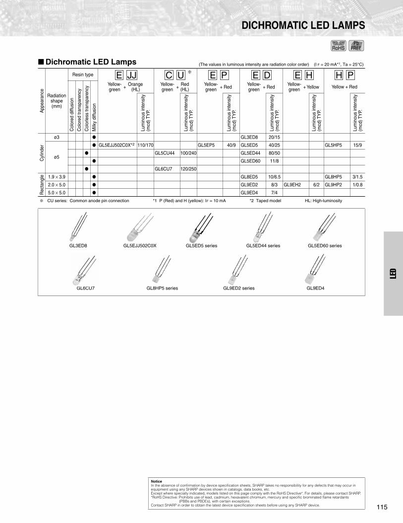
115
LED
DICHROMATIC LED LAMPS
Dichromatic LED Lamps
CU series: Common anode pin connection *1 P (Red) and H (yellow): I
F
= 10 mA *2 Taped model HL: High-luminosity
App
eara
nce
Radiation shape (mm)
Resin type
Col
ored
diff
usio
n
Col
ored
tran
spar
ency
Col
orle
ss tr
ansp
aren
cy
Milk
y di
ffusi
on
Yellow- Orange green (HL)
Yellow- Red green (HL)
Yellow- green
Yellow- green
Yellow- green Yellow + Red
Lum
inou
s in
tens
ity
(mcd
) TY
P.
Lum
inou
s in
tens
ity
(mcd
) TY
P.
Lum
inou
s in
tens
ity
(mcd
) TY
P.
Lum
inou
s in
tens
ity
(mcd
) TY
P.
Lum
inou
s in
tens
ity
(mcd
) TY
P.
Lum
inou
s in
tens
ity
(mcd
) TY
P.
Cyl
inde
r
ø3
GL3ED8 20/15
ø5
GL5EJJ502C0X*
2
110/170 GL5EP5 40/9 GL5ED5 40/25 GL5HP5 15/9
GL5CU44 100/240 GL5ED44 80/50
GL5ED60 11/8
GL6CU7 120/250
Rec
tang
le 1.9
×
3.9
GL8ED5 10/6.5 GL8HP5 3/1.5
2.0
×
5.0
GL9ED2 8/3 GL9EH2 6/2 GL9HP2 1/0.8
5.0
×
5.0
GL9ED4 7/4
GL3ED8 GL5EJJ502C0X GL5ED5 series GL5ED44 series GL5ED60 series
GL6CU7 GL8HP5 series GL9ED2 series GL9ED4
(The values in luminous intensity are radiation color order) (I F = 20 mA*1, Ta = 25°C)
E JJ C U E P E D E H H P+ + + Red + Red + Yellow
Notice
In the absence of confirmation by device specification sheets, SHARP takes no responsibility for any defects that may occur in equipment using any SHARP devices shown in catalogs, data books, etc.Except where specially indicated, models listed on this page comply with the RoHS Directive*. For details, please contact SHARP.*RoHS Directive: Prohibits use of lead, cadmium, hexavalent chromium, mercury and specific brominated flame retardants (PBBs and PBDEs), with certain exceptions.Contact SHARP in order to obtain the latest device specification sheets before using any SHARP device.
"

LED
116
HIGH-LUMINOSITY CHIP LEDs
New product
Under development
High-Luminosity (AlGaInP) Chip LEDs (Taped Models Only)
*1 LT1JS67A, LT1JV67A, GM1JV55200AE series, GM1JV35200AE series, GM1JV40300AE series: I
F
= 5 mA*2 GM5ZR01200A series, GM5ZR03200Z series: IF = 60 mA*3 GM5ZV96260AE series, GM5ZV96270A series, GM5ZV01200A series, GM5ZV03200Z series: Tc= 25°C
High-Luminosity (InGaN) Chip LEDs (Taped Models Only)
*1 GM1BC35370AC, GM1BC55255AC: I
F
= 5 mA*2 GM5BC96260AC series, GM5BC96270A series, GM4BC83200AC series, GM5BC05240AC series: I
F
= 20 mA*3 GM5BC01250AC series, GM5BC03210Z series: I
F
= 50 mA*4 GM1GC55310AC: I
F
= 10 mA*5 GM5BC96260AC series, GM5BC96270A series, GM5BC01250AC series, GM5BC03210Z series: Tc= 25°C
Outline dimensions
(mm)
Resin typeC
olor
ed d
iffus
ion
Col
ored
tran
spar
ency
Col
orle
ss tr
ansp
aren
cy
Milk
y di
ffusi
on
Yellow-green
Lum
inou
s in
tens
ity
(mcd
) TY
P. Amber
Lum
inou
s in
tens
ity
(mcd
) TY
P. Sunset orange
Lum
inou
s in
tens
ity
(mcd
) TY
P. Orange
Lum
inou
s in
tens
ity
(mcd
) TY
P. Red
Lum
inou
s in
tens
ity
(mcd
) TY
P.
1.6
×
0.8 (T: 0.35)
GM1JE35200AE*
1
13
GM1JV35200AE*
1
18.8
GM1JS35200AE*
1
19
GM1JJ35200AE*
1
19
GM1JR35200AE*
1
13
1.6
×
0.8 (T: 0.55)
GM1JE55200AE*
1
13
GM1JV55200AE*
1
16.8
GM1JS55200AE*
1
20.9
GM1JJ55200AE*
1
19
1.6
×
0.8 (T: 0.8)
GM1ZV80300AE
75
GM1ZS80300AE
75
GM1ZJ80300AE
75
GM1ZR80300AE
55
LT1JV67A*
1
16.5
LT1JS67A*
1
14.1
2.0
×
1.25 (T: 0.8)
GM1ZV40300AE
60
GM1ZS40300AE
78
GM1ZJ40300AE
60
GM1ZR40300AE
55
GM1JV40300AE
11
GM1JS40300AE
12
GM1JJ40300AE
9.5
3.2
×
2.8 (T: 1.9)
GM5ZV96270A
600
GM5ZR96270A
600
GM5ZV96260AE
320
GM5ZR96260AE
300
6.0
×
5.0 (T: 2.5)
GM5ZV01200A*
2
500
GM5ZS01200A*
2
700
GM5ZJ01200A*
2
500
GM5ZR01200A*
2
400
GM5SE01200A*
2
400
GM5SJ01250AL
1 050
6.0
×
5.0 (T: 2.3)
(board insertion type)
GM5ZV03200Z*
2
500
GM5ZS03200Z*
2
700
GM5ZJ03200Z*
2
500
GM5ZR03200Z*
2
400
2.8
×
1.2 (T: 0.8) (Side emitting)
GM4ZV83200AE
(100)
GM4ZS83200AE
(150)
GM4ZJ83200AE
(150)
GM4ZR83200AE
(90)
5.0
×
5.0 (T: 1.5)
GM5ZR05240A
3 000
Outline dimensions
(mm)
Resin type
Col
ored
di
ffusi
on
Col
ored
tra
nspa
renc
y
Col
orle
ss
trans
pare
ncy
Milk
y di
ffusi
on
Blue GreenLuminous intensity
(mcd) TYP.
Luminous intensity
(mcd) TYP.
1.6
×
0.8 (T: 0.35)
GM1BC35370AC*
1
23
1.6
×
0.8 (T: 0.55)
GM1BC55255AC*
1
23
GM1GC55310AC*
4
100
3.2
×
2.8 (T: 1.9)
GM5BC96270A*
2
500
GM5GC96270A 1 300
GM5BC96260AC*
2
300
GM5GC96260AC*
2
700
6.0
×
5.0 (T: 2.5)
GM5BC01250AC*
3
400
GM5GC01250AC*
3
1 200
6.0
×
5.0 (T: 2.3)board insertion type
GM5BC03210Z*
3
400
GM5GC03210Z*
3
1 200
2.8
×
1.2 (T: 0.8)Side emitting
GM4BC83200AC*2 (150) GM4GC83200AC*2 (300)
5.0 × 5.0 (T: 1.5) GM5BC05240AC*2 2 000 GM5GC05240AC*2 4 000
(I F = 20 mA, Ta = 25°C*3)
S EJ E J VZ V J SZ S J JZ JS J
J RZ R
(I F = 10 mA, Ta = 25°C*5)
B C G C
NoticeIn the absence of confirmation by device specification sheets, SHARP takes no responsibility for any defects that may occur in equipment using any SHARP devices shown in catalogs, data books, etc.Except where specially indicated, models listed on this page comply with the RoHS Directive*. For details, please contact SHARP.*RoHS Directive: Prohibits use of lead, cadmium, hexavalent chromium, mercury and specific brominated flame retardants (PBBs and PBDEs), with certain exceptions.Contact SHARP in order to obtain the latest device specification sheets before using any SHARP device.
#

117
LED
CHIP LEDs
Chip LEDs (Taped Models Only)
*1 P (Red) series: I
F
= 5 mA HL: High-luminosity
High-Luminosity Dichromatic Type Chip LEDs (Taped Models Only)
Outline dimensions (mm)
Resin type
Col
ored
diff
usio
n
Col
ored
tran
spar
ency
Col
orle
ss tr
ansp
aren
cy
Milk
y di
ffusi
on
Green
Lum
inou
s in
tens
ity
(mcd
) TY
P. Yellow-green
Lum
inou
s in
tens
ity
(mcd
) TY
P. Yellow
Lum
inou
s in
tens
ity
(mcd
) TY
P.
1.6
×
0.8 (T: 0.35)
GM1EG35200A 191.6
×
0.8 (T: 0.55)
GM1EG55200A 19 GM1HY55200A 11.5
1.6
×
0.8 (T: 0.8)
LT1K67A 3.8LT1E67ALT1F67ALT1F67AF
23 LT1H67A 8.3
2.0
×
1.25 (T: 0.8)
LT1K40A 5 LT1E40A 19 LT1H40A 10.83.2
×
2.8 (T: 1.9)
GM5EG95200A 18.1
Outline dimensions (mm)
Resin type
Col
ored
diff
usio
n
Col
ored
tran
spar
ency
Col
orle
ss tr
ansp
aren
cy
Milk
y di
ffusi
on
Sunset orange
Lum
inou
s in
tens
ity
(mcd
) TY
P. Red
Lum
inou
s in
tens
ity
(mcd
) TY
P. Red (HL)
Lum
inou
s in
tens
ity
(mcd
) TY
P.
Red
Lum
inou
s in
tens
ity
(mcd
) TY
P.
1.6
×
0.8 (T: 0.55)
GM1HS55200A 11.4 GM1HD55200A 12.5 GM1UR55200A 29.71.6
×
0.8 (T: 0.8)
LT1S67A 6.9 LT1D67A 8.8 LT1U67A 29.7 LT1P67A 1.32.0
×
1.25 (T: 0.8)
LT1S40A 9.4 LT1D40A 11.9 LT1U40A 35.6 LT1P40A 1.33.2
×
2.8 (T: 1.9)
GM5HD95200A 13.8 GM5UR95200A 80
LT1D67A seriesLT1JS67A series
GM1ZV80300AE series
GM1EG55200A seriesGM1JV55200AE seriesGM1BC55255AC series
LT1E40A seriesGM1JV40300AE seriesGM1ZV40300AE series
GM1JV35200AE seriesGM1EG35200A
GM1BC35370AC
GM4ZV83200AE seriesGM4BC83200AC series
GM5ZR05240AGM5BC05240AC series
GM5EG95200A series GM5ZV96260AE series, GM5BC96260AC series
GM5BC96270A series
GM5ZR01200A series GM5BC01250AC series
GM5ZV03200Z seriesGM5BC03210Z series
Taped model
Outline dimensions
(mm)
Resin type
Col
ored
di
ffusi
on
Col
ored
tra
nspa
renc
y
Col
orle
ss
trans
pare
ncy
Milk
y di
ffusi
on
Blue + Green Blue + Red Green + RedLuminous intensity
(mcd) TYP.
Luminous intensity
(mcd) TYP.
Luminous intensity
(mcd) TYP.
6.0
×
5.0 (T: 2.5)
GM5BG01210A 300/860 GM5ZRB01210A 300/580 GM5ZRG01210A 860/580
(IF = 20 mA*1, Ta = 25°C)
K E F E G H H Y
S H S D H D U U R P
(I F = 40 mA, Tc = 25°C)
BC GC BC ZR GC ZR
Notice
In the absence of confirmation by device specification sheets, SHARP takes no responsibility for any defects that may occur in equipment using any SHARP devices shown in catalogs, data books, etc.Except where specially indicated, models listed on this page comply with the RoHS Directive*. For details, please contact SHARP.*RoHS Directive: Prohibits use of lead, cadmium, hexavalent chromium, mercury and specific brominated flame retardants (PBBs and PBDEs), with certain exceptions.Contact SHARP in order to obtain the latest device specification sheets before using any SHARP device.
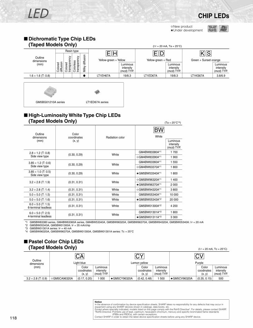
LED
118
CHIP LEDs
New product
Under development
Dichromatic Type Chip LEDs (Taped Models Only)
High-Luminosity White Type Chip LEDs (Taped Models Only)
*1 GM5BW83380 series, GM4BW63360A series, GM4BW53340A, GM5BW96320A, GM5BW96370A, GM5BW94320A, GM5BW05340A: I
F
= 20 mA*2 GM5BW05343A, GM5BW01300A: I
F
= 35 mA/chip*3 GM5BW01301A series: I
F
= 40 mA*4 GM5BW96320A, GM5BW96370A, GM5BW01300A, GM5BW01301A series: Tc = 25°C
Pastel Color Chip LEDs (Taped Models Only)
Outline dimensions
(mm)
Resin type
Col
ored
di
ffusi
on
Col
ored
tra
nspa
renc
y
Col
orle
ss
trans
pare
ncy
Milk
y di
ffusi
on
Yellow-green + Yellow Yellow-green + Red Green + Sunset orangeLuminous intensity
(mcd) TYP.
Luminous intensity
(mcd) TYP.
Luminous intensity
(mcd) TYP.
1.6
×
1.6 (T: 0.8)
LT1EH67A 19/8.3 LT1ED67A 19/8.3 LT1KS67A 3.8/6.9
GM5BG01210A series LT1ED67A series
Outline dimensions
(mm)
Color coordinates
(x, y)Radiation color White
Luminous intensity
(mcd) TYP.
2.8
×
1.2 (T: 0.8)Side view type (0.30, 0.29) White
GM4BW83380A*
1
1 700
GM4BW83390A*
1
1 900
3.85
×
1.2 (T: 0.6)Side view type (0.30, 0.29) White
GM4BW63360A*
1
1 550
GM4BW63370A*
1
1 800
3.85
×
1.0 (T: 0.5)Side view type (0.30, 0.29) White
GM5BW53340A*
1
1 800
3.2
×
2.8 (T: 1.9) (0.31, 0.31) White
GM5BW96320A*
1
1 400
GM5BW96370A*
1
2 000
3.2
×
2.8 (T: 1.4) (0.31, 0.31) White
GM5BW94320A*
1
3 800
5.0
×
5.0 (T: 1.5) (0.31, 0.31) White GM5BW05340A*
1
10 000
5.0
×
5.0 (T: 1.6) (0.31, 0.31) White
GM5BW05343A*
2
20 000
6.0
×
5.0 (T: 1.5) 6-terminal leadless (0.31, 0.31) White GM5BW01300A*
2
4 200
6.0
×
5.0 (T: 2.5) 4-terminal leadless (0.31, 0.31) White
GM5BW01301A*
3
1 800
GM5BW01311A*
3
3 300
Outline dimensions
(mm)Light blue Lemon yellow Purple
Color coodinates
(x, y)
Luminous intensity
(mcd) TYP.
Color coodinates
(x, y)
Luminous intensity
(mcd) TYP.
Color coodinates
(x, y)
Luminous intensity
(mcd) TYP.
3.2
×
2.8 (T: 0.9)
GM5CA96320A (0.17, 0.20) 1 000
GM5CY96320A (0.42, 0.48) 1 500
GM5CV96320A (0.35, 0.15) 500
(I F = 20 mA, Ta = 25°C)
HE DE SK
(Ta = 25°C*4)
BW
(I F = 20 mA, Tc = 25°C)
CA CY CV
Notice
In the absence of confirmation by device specification sheets, SHARP takes no responsibility for any defects that may occur in equipment using any SHARP devices shown in catalogs, data books, etc.Except where specially indicated, models listed on this page comply with the RoHS Directive*. For details, please contact SHARP.*RoHS Directive: Prohibits use of lead, cadmium, hexavalent chromium, mercury and specific brominated flame retardants (PBBs and PBDEs), with certain exceptions.Contact SHARP in order to obtain the latest device specification sheets before using any SHARP device.

119
LED
CHIP LEDs / LEDs FOR CAMERA DATA BACK
New product
Under development
High-Luminosity Dichromatic Type Chip LEDs (RGB 3-color) (Taped Models Only)
*1 GM5WA06260A: I
F
= 40 mA (Red, Green), I
F
= 20 mA (Blue)*2 GM5WA06250A, GM5WA06250Z: I
F
= 35 mA (Red, Green), I
F
= 20 mA (Blue)*3 GM5WA06270A: I
F
= 35 mA (Red, Green, Blue)*4 GM5WA06270A: T: 2.4 mm*5 GM1WA55311A/GM4WA10200A: I
F
= 5 mA (Red, Green, Blue)*6 GM5WA06256A: I
F
= 22 mA (Red), I
F
= 35 mA (Green), I
F
= 13 mA (Blue)*7 GM5WA94200A: I
F
= 17 mA (Red), I
F
= 20 mA (Green), I
F
= 10 mA (Blue)*8 GM4WA25300A: I
F
= 21 mA (Red), I
F
= 25 mA (Green), I
F
= 7 mA (Blue)*9 GM5WA94200A, GM4WA10200A, GM4WA25300A, GM5WA06250A series: Tc = 25°C
LEDs for Camera Data Back
( ) indicates reference value.
GM5BW96320A GM5BW96370A GM5CA96320A
series
GM5BW01300A GM5BW01301AGM5BW01311A
GM4BW83380A series
GM4BW53340A GM5BW05340AGM5BW05343A
GM4BW63360A series
Outline dimensions
(mm)
Resin type
Col
ored
di
ffusi
on
Col
ored
tra
nspa
renc
y
Col
orle
sstra
nspa
renc
y
Milk
y di
ffusi
on Red + Green + Blue
Luminous intensity (mcd) TYP.
1.6
×
1.6 (T: 0.55)
GM1WA55311A*
5
20/70/23
2.7
×
1.35 (T: 1.0)Side view type
GM4WA10200A*
5
10 to 40/16 to 100/10 to 42
3.2
×
2.8 (T: 1.4)
GM5WA94200A*
7
(920) [Mixed color]
5.0
×
2.5 (T: 2.5)
GM4WA25300A*
8
(2 000) [Mixed color]
6.0
×
5.0 (T: 2.5) 6-terminal leadless
GM5WA06250A*
2
1 400 [Mixed color]
GM5WA06260A*
1
1 725 [Mixed color]
GM5WA06256A*
6
1 500 [Mixed color]
GM5WA06270A*
3, 4
3 000 [Mixed color]
6.0
×
5.0(T: 2.3 [resin part])
6-terminal
GM5WA06250Z*
2
1 400 [Mixed color]
GM5WA06256Z*
6
1 500 [Mixed color]
GM1WA55311A GM5WA06250AGM5WA06260AGM5WA06256A
GM5WA06250ZGM5WA06256Z
GM5WA06270A GM5WA94200A GM4WA10200A GM4WA25300A
Model No. No. of dots Outline dimensions (mm) Radiation color Luminous intensity (mcd)
GW01M59001PE 7 2.6
×
2.9 (T: 0.9) Surface-mount type Amber (MIN. 0.4 TYP. 0.8)
GW01M59001PE
(Ta = 25°C*11)
WA
(IF = 1 mA, Ta = 25°C)
Notice
In the absence of confirmation by device specification sheets, SHARP takes no responsibility for any defects that may occur in equipment using any SHARP devices shown in catalogs, data books, etc.Except where specially indicated, models listed on this page comply with the RoHS Directive*. For details, please contact SHARP.*RoHS Directive: Prohibits use of lead, cadmium, hexavalent chromium, mercury and specific brominated flame retardants (PBBs and PBDEs), with certain exceptions.Contact SHARP in order to obtain the latest device specification sheets before using any SHARP device.

LASER
120
LASER DIODES
New product
Laser Diodes
Model Configurations
*1 Optical power output (CW) MAX. (mW)
Specifications
• Terminal Connections
Wavelength (nm)
Optical power output (Pulse)
(mW) MAX.
Package
ø5.6 mmMetal type
ø3.3 mmMetal type
1.8 mm tResin type
ø5.6 mmResin type
405 band 20*
1
GH04020A2GE
650 band
240 GH06P24A2C GH16P24A8C
300
GH16P30A8C
350
GH16P35A8C
780 band
5*
1
GH07805C2K GH17805B2AS
25*
1
GH07825C2K
240 GH07P24C1C GH07P24C4C GH17P24C8C
280 GH07P28A1C GH07P28A4C
GH17P28A8C
Model No.Wave-length(nm)
Optical power output (mW)
MAX. Features Applications
Terminal connec-
tions
CW Pulse
GH04020A2GE 405 band 20 — ø5.6 mm CAN package, operating temperature: 70°C MAX. Next generation DVD playback E
GH06P24A2C
650 band
100 240 ø5.6 mm CAN package, operating temperature: 75°C MAX. (pulse drive) Double-layer DVD
×
4 writing BGH16P24A8C 100 240 1.8 mm frame package, operating temperature: 75°C MAX. (pulse drive) Double-layer DVD
×
4 writingCGH16P30A8C 120 300 1.8 mm frame package, operating temperature: 75°C MAX. (pulse drive) Double-layer DVD
×
8 writingGH16P35A8C 125 350 1.8 mm frame package, operating temperature: 75°C MAX. (pulse drive) Double-layer DVD
×
16 writing
GH17805B2AS
780 band
5 — ø5.6 mm frame package, operating temperature: 70°C MAX.,with built-in monitor PD CD-ROM, CD-Audio A
GH07805C2K 5 — ø5.6 mm CAN package, operating temperature: 60°C MAX.,with built-in monitor PD Printer, copier, complex machine
DGH07825C2K 25 — ø5.6 mm CAN package, operating temperature: 60°C MAX.,
with built-in monitor PD Printer, copier, complex machine
GH07P24C1C 120 240 ø5.6 mm CAN package, operating temperature: 75°C MAX. (pulse drive) CD-R/RW (MAX.
×
48 to
×
52 writing)
B
GH07P28A1C 150 280 ø5.6 mm CAN package, operating temperature: 75°C MAX. (pulse drive) CD-R/RW (MAX.
×
48 to
×
52 writing)
GH07P24C4C 120 240 ø3.3 mm CAN package, operating temperature: 75°C MAX. (pulse drive) CD-R/RW (H/H, slim dual-purpose) (MAX.
×
48 to
×
52 writing)
GH07P28A4C 150 280 ø3.3 mm CAN package, operating temperature: 75°C MAX. (pulse drive) CD-R/RW (H/H, slim dual-purpose) (MAX.
×
48 to
×
52 writing)
GH17P24C8C 120 240 1.8 mm frame package, operating temperature: 75°C MAX. (pulse drive) CD-R/RW (H/H, slim dual-purpose) (MAX.
×
48 to
×
52 writing)C
GH17P28A8C 150 280 1.8 mm frame package, operating temperature: 75°C MAX. (pulse drive) CD-R/RW (H/H, slim dual-purpose) (MAX.
×
48 to
×
52 writing)
A B C D E
(Tc = 25°C)
1 3
2
Photodiode
Stem
Laser diode
1 3
2
Laser diode
Stem
Laser diode
3
4 21
GND
Laser diodePhotodiode
13
2 Stem
Laser diode
2 Stem
13
Notice
In the absence of confirmation by device specification sheets, SHARP takes no responsibility for any defects that may occur in equipment using any SHARP devices shown in catalogs, data books, etc. Except where specially indicated, models listed on this page comply with the RoHS Directive*. For details, please contact SHARP.*RoHS Directive: Prohibits use of lead, cadmium, hexavalent chromium, mercury and specific brominated flame retardants (PBBs and PBDEs), with certain exceptions.Contact SHARP in order to obtain the latest device specification sheets before using any SHARP device.

RF
121
RF C
ompo
nent
s
LOW NOISE BLOCKDOWN CONVERTER
Europe: LNB for Broadcasting Satellite
Features
(1) Wide band type receiving all broadcasting channels (analog & digital) of Europe. [Universal LNB]
(2) Originally developed feed-horn waveguide makes the wide-band, low-noise characteristics possible.
(3) One of the industry’s most compact and lightweight package
(4) Low consumption current design for energy saving [80 mA (TYP.): BS1R8EL100A]
Specifications
U.S.A.: LNB for FSS Broadcast/(Others: LNB for Communication)
Specifications
Destination Europe, Astra/Eutelsat Satellite etc.Receiving polarization Horizontal/Vertical polarizationModel No. <Type> BS1R8EL500A <4 output> BS1R8EL400A <4 output> BS1R8EL200A <2 output> BS1R8EL100A <1 output>Input frequency (GHz) 10.7 to 11.7 [Low band], 11.7 to 12.75 [High band]Output frequency (MHz) 950 to 1 950 [Low band], 1 100 to 2 150 [High band]Local oscillation frequency (GHz) 9.75 [Low band], 10.6 [High band]NF (dB) 0.7 (TYP.)Conversion gain (dB) 56 (TYP.)Phase noise –55 dBc/Hz @1 kHz (TYP.)Cross-polar discrimination (dB) 25 (TYP.)
Supply voltage (V DC)(Polarization switching voltage)
Vertical polarization 11.5 to 14.0 (0/22 kHz)Horizontal polarization 16.0 to 19.0 (0/22 kHz)
Power consumption (mA) 210 (TYP.)/250 (MAX.) 310 (TYP.)/350 (MAX.) 190 (TYP.)/250 (MAX.) 80 (TYP.)/120 (MAX.)Waveguide Feed-horn (F/D = 0.6)Output impedance (
Ω
) 75
Output connector (F-type) 4-output (H/H, H/L, V/H, V/L)
4-output (H/V, High and low switching)
2-output (H/V, High and low switching)
1-output (H/V, High and low switching)
Outline dimensions (mm) 133.0
×
103.6
×
60.0 133.0
×
103.6
×
60.0 123.5
×
97.0
×
60.0 107.3
×
60.0
×
60.0Weight (g) Approx. 255 Approx. 256 Approx. 215 Approx. 110
BS1R8EL500A BS1R8EL400A BS1R8EL200A BS1R8EL100A
Receiving system U.S.A.: FSS, Japan and others: for communicationReceiving polarization Horizontal/vertical polarizationModel No. BS1C1UR100AInput frequency (GHz) 11.7 to 12.2Output frequency (MHz) 950 to 1 450Local oscillation frequency (GHz) 10.75NF (dB) 0.7 (TYP.)/0.9 (MAX.)Conversion gain (dB) 50 to 62Phase noise -60 dBc/Hz @1 kHz (TYP.)Cross-polar discrimination (dB) —Supply voltage (V DC) 12 to 24Power consumption (mA) 120 (TYP.)/150 (MAX.)Waveguide WR-75Output impedance (
Ω
) 75Output connector (F-type) 1-outputOutline dimensions (mm) 48.6
×
96.3
×
45.5 BS1C1UR100A
Weight (g) Approx. 100
Notice
In the absence of confirmation by device specification sheets, SHARP takes no responsibility for any defects that may occur in equipment using any SHARP devices shown in catalogs, data books, etc. Contact SHARP in order to obtain the latest device specification sheets before using any SHARP device.
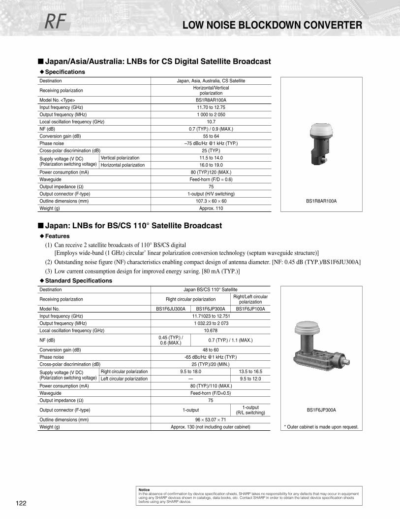
RF
122
LOW NOISE BLOCKDOWN CONVERTER
Japan/Asia/Australia: LNBs for CS Digital Satellite Broadcast
Specifications
Japan: LNBs for BS/CS 110° Satellite Broadcast
Features
(1) Can receive 2 satellite broadcasts of 110° BS/CS digital [Employs wide-band (1 GHz) circular’ linear polarization conversion technology (septum waveguide structure)]
(2) Outstanding noise figure (NF) characteristics enabling compact design of antenna diameter. [NF: 0.45 dB (TYP.)/BS1F6JU300A]
(3) Low current consumption design for improved energy saving. [80 mA (TYP.)]
Standard Specifications
Destination Japan, Asia, Australia, CS Satellite
Receiving polarization Horizontal/Vertical polarization
Model No. <Type> BS1R8AR100A
Input frequency (GHz) 11.70 to 12.75
Output frequency (MHz) 1 000 to 2 050
Local oscillation frequency (GHz) 10.7
NF (dB) 0.7 (TYP.) / 0.9 (MAX.)
Conversion gain (dB) 55 to 64
Phase noise –75 dBc/Hz @1 kHz (TYP.)
Cross-polar discrimination (dB) 25 (TYP.)
Supply voltage (V DC)
(Polarization switching voltage)
Vertical polarization 11.5 to 14.0
Horizontal polarization 16.0 to 19.0
Power consumption (mA) 80 (TYP.)120 (MAX.)
Waveguide Feed-horn (F/D = 0.6)
Output impedance (
Ω
) 75
Output connector (F-type) 1-output (H/V switching)
Outline dimensions (mm) 107.3
×
60
×
60 BS1R8AR100A
Weight (g) Approx. 110
Destination Japan BS/CS 110° Satellite
Receiving polarization Right circular polarization Right/Left circular polarization
Model No. BS1F6JU300A BS1F6JP300A BS1F6JP100A
Input frequency (GHz) 11.71023 to 12.751
Output frequency (MHz) 1 032.23 to 2 073
Local oscillation frequency (GHz) 10.678
NF (dB) 0.45 (TYP.) / 0.6 (MAX.) 0.7 (TYP.) / 1.1 (MAX.)
Conversion gain (dB) 48 to 60
Phase noise -65 dBc/Hz @1 kHz (TYP.)
Cross-polar discrimination (dB) 25 (TYP.)/20 (MIN.)
Supply voltage (V DC)
(Polarization switching voltage)Right circular polarization
9.5 to 18.0 13.5 to 16.5
Left circular polarization — 9.5 to 12.0
Power consumption (mA) 80 (TYP.)/110 (MAX.)
Waveguide Feed-horn (F/D=0.5)
Output impedance (
Ω
) 75
Output connector (F-type) 1-output 1-output (R/L switching) BS1F6JP300A
Outline dimensions (mm) 96
×
53.07
×
71
Weight (g) Approx. 130 (not including outer cabinet) * Outer cabinet is made upon request.
Notice
In the absence of confirmation by device specification sheets, SHARP takes no responsibility for any defects that may occur in equipment using any SHARP devices shown in catalogs, data books, etc. Contact SHARP in order to obtain the latest device specification sheets before using any SHARP device.

123
RF C
ompo
nent
s
DIGITAL DBS FRONT-END UNITS
Digital DBS Front-End Units
BS front-end unit for digital broadcasting features high quality of signal transmission and improved elimination ability of various kinds of rejection thanks to using Sharp’s original ICs.
Features
(1) Equipped with a direct conversion IC developed by Sharp. Reliability is improved by reducing power consumption and component counts.
(2) Wide-band reception design also covering CS broadcast band. [Reception frequency: 950 to 2 150 MHz]
(3) Wide product line-up of LINK integrated types for contributing to set development time reduction. [Compatible with DVB-S/DVB-S2/ISDB-S demodulation]
(4) User support tools can be provided. [Sample/evaluation boards and software are available.]
Standard Specifications <IQ output type>
Contact SHARP for custom design product. (Vertical chassis compatible)*1 I
2
C-bus is a trademark of Philips Corporation.
Destination Global
Demodulator system DVB-S ISDB-S/DVB-S2
Input type 1-input/1-loop through output 1-input
Model No. BS2S7HZ0502 BS2S7HZ6306
Input frequency (MHz) 950 to 2 150
Input signal level (dBm) –65 to –25
The 1st intermediate frequency (MHz) Zero-IF (Direct conversion)
Base band frequency bandwidth 10 to 30, 2.0 MHz step (BB LPF)
RF input local leak (dBm) –70 and below BS2S7HZ0502
PLL phase noise (dBc/Hz)
10 kHz offset –80 (TYP.) –85 (TYP.)
1 kHz offset –75 (TYP.) –80 (TYP.)
Output type I/Q
Channel selection system PLL (I
2
C-bus)*
1
Noise figure (dB) 7 (TYP.)
Tuning voltage (V DC) Shared with a 3.3 V power source
Supply voltage (V DC) 3.3
LNB power supply DC 25 V, 400 mA (MAX.)
Input impedance (
Ω
) 75 BS2S7HZ6306
Outline dimensions (mm) 29.6
×
29.4
×
13.0 30.6
×
25.0
×
13.0
D
Notice
In the absence of confirmation by device specification sheets, SHARP takes no responsibility for any defects that may occur in equipment using any SHARP devices shown in catalogs, data books, etc. Contact SHARP in order to obtain the latest device specification sheets before using any SHARP device.
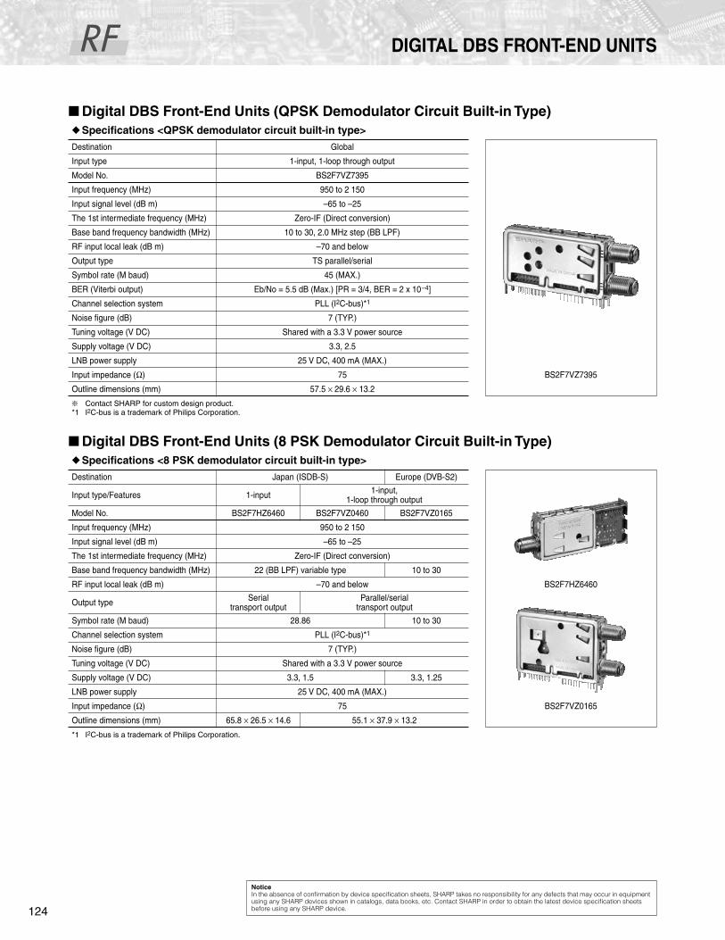
RF
124
DIGITAL DBS FRONT-END UNITS
Digital DBS Front-End Units (QPSK Demodulator Circuit Built-in Type)
Specifications <QPSK demodulator circuit built-in type>
Contact SHARP for custom design product.*1 I
2
C-bus is a trademark of Philips Corporation.
Digital DBS Front-End Units (8 PSK Demodulator Circuit Built-in Type)
Specifications <8 PSK demodulator circuit built-in type>
*1 I
2
C-bus is a trademark of Philips Corporation.
Destination Global
Input type 1-input, 1-loop through output
Model No. BS2F7VZ7395
Input frequency (MHz) 950 to 2 150
Input signal level (dB m) –65 to –25
The 1st intermediate frequency (MHz) Zero-IF (Direct conversion)
Base band frequency bandwidth (MHz) 10 to 30, 2.0 MHz step (BB LPF)
RF input local leak (dB m) –70 and below
Output type TS parallel/serial
Symbol rate (M baud) 45 (MAX.)
BER (Viterbi output) Eb/No = 5.5 dB (Max.) [PR = 3/4, BER = 2 x 10
–4
]
Channel selection system PLL (I
2
C-bus)*
1
Noise figure (dB) 7 (TYP.)
Tuning voltage (V DC) Shared with a 3.3 V power source
Supply voltage (V DC) 3.3, 2.5
LNB power supply 25 V DC, 400 mA (MAX.)
Input impedance (
Ω
) 75 BS2F7VZ7395
Outline dimensions (mm) 57.5
×
29.6
×
13.2
Destination Japan (ISDB-S) Europe (DVB-S2)
Input type/Features 1-input 1-input, 1-loop through output
Model No. BS2F7HZ6460 BS2F7VZ0460 BS2F7VZ0165
Input frequency (MHz) 950 to 2 150
Input signal level (dB m) –65 to –25
The 1st intermediate frequency (MHz) Zero-IF (Direct conversion)
Base band frequency bandwidth (MHz) 22 (BB LPF) variable type 10 to 30
RF input local leak (dB m) –70 and below BS2F7HZ6460
Output type Serial transport output
Parallel/serial transport output
Symbol rate (M baud) 28.86 10 to 30
Channel selection system PLL (I
2
C-bus)*
1
Noise figure (dB) 7 (TYP.)
Tuning voltage (V DC) Shared with a 3.3 V power source
Supply voltage (V DC) 3.3, 1.5 3.3, 1.25
LNB power supply 25 V DC, 400 mA (MAX.)
Input impedance (
Ω
) 75 BS2F7VZ0165
Outline dimensions (mm) 65.8
×
26.5
×
14.6 55.1
×
37.9
×
13.2
Notice
In the absence of confirmation by device specification sheets, SHARP takes no responsibility for any defects that may occur in equipment using any SHARP devices shown in catalogs, data books, etc. Contact SHARP in order to obtain the latest device specification sheets before using any SHARP device.
!
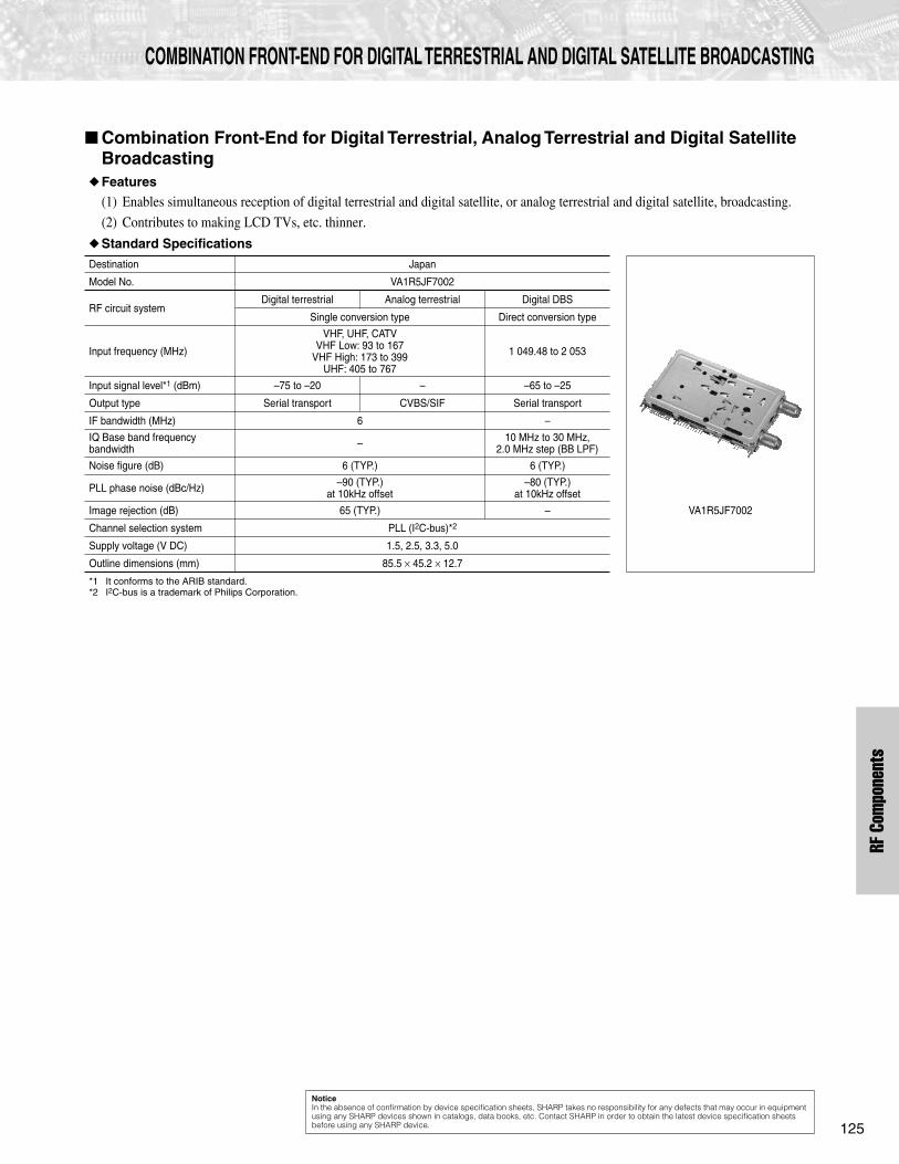
125
RF C
ompo
nent
s
COMBINATION FRONT-END FOR DIGITAL TERRESTRIAL AND DIGITAL SATELLITE BROADCASTING
Combination Front-End for Digital Terrestrial, Analog Terrestrial and Digital Satellite Broadcasting
Features
(1) Enables simultaneous reception of digital terrestrial and digital satellite, or analog terrestrial and digital satellite, broadcasting.
(2) Contributes to making LCD TVs, etc. thinner.
Standard Specifications
*1 It conforms to the ARIB standard.*2 I
2
C-bus is a trademark of Philips Corporation.
Destination Japan
Model No. VA1R5JF7002
RF circuit systemDigital terrestrial Analog terrestrial Digital DBS
Single conversion type Direct conversion type
Input frequency (MHz)
VHF, UHF, CATVVHF Low: 93 to 167
VHF High: 173 to 399UHF: 405 to 767
1 049.48 to 2 053
Input signal level*
1
(dBm) –75 to –20 – –65 to –25
Output type Serial transport CVBS/SIF Serial transport
IF bandwidth (MHz) 6 –
IQ Base band frequency bandwidth – 10 MHz to 30 MHz,
2.0 MHz step (BB LPF)
Noise figure (dB) 6 (TYP.) 6 (TYP.)
PLL phase noise (dBc/Hz) –90 (TYP.)at 10kHz offset
–80 (TYP.)at 10kHz offset
Image rejection (dB) 65 (TYP.) – VA1R5JF7002
Channel selection system PLL (I
2
C-bus)*
2
Supply voltage (V DC) 1.5, 2.5, 3.3, 5.0
Outline dimensions (mm) 85.5
×
45.2
×
12.7
Notice
In the absence of confirmation by device specification sheets, SHARP takes no responsibility for any defects that may occur in equipment using any SHARP devices shown in catalogs, data books, etc. Contact SHARP in order to obtain the latest device specification sheets before using any SHARP device.
"

RF
126
DIGITAL TERRESTRIAL FRONT-END UNIT
Front-End Units for ISDB-T/DVB-T
Features
(1) Low phase noise characteristics, high elimination of adjacent channel interference.
(2) Transport stream output front-end units with built-in OFDM demodulation IC. [VA1L5JF6013/VA1J5ED5055]
(3) Compact, low power consumption.
(4) Other types are available with various forms of chassis (vertical or horizontal type) and input connectors (F or DIN type), etc.
Standard Specifications
*1 Enables simultaneous reception of digital terrestrial and digital satellite broadcasting.*2 I
2
C-bus is a trademark of Philips Corporation.*3 During simultaneous OFDM/8PSK demodulation operation.
Destination Japan Europe/Asia
Product name ISDB-T/S front end (built-in OFDM/8PSK demodulation) DVB-T front end (IF output)
DVB-T front end (built-in OFDM demodulation)
Model No. VA1J5JF7007 VA1T1ED5065 VA1H1ED5265 VA1K5ED5255
Input frequency (MHz)*
1
VHF, UHF, CATVVHF Low: 93 to 167
VHF High: 173 to 399 UHF: 405 to 767
1 049.48 to 2 053 VHF: 143.5 to 430 UHF: 430 to 862
VHF: 146 to 430 UHF: 430 to 862
Output Transport stream(Built-in OFDM/8PSK demodulation) Direct IF
Transport stream(Built-in OFDM demodulation)
IF bandwidth (MHz) 6 — 7, 8, selectable
Mode Mode 1, 2, 3 2k, 8k, both compatible
Input sensitivity–79 dBm (TYP.)
[in mode 3, 64 QAM, CR = 7/8 (QEF)]
–85 dBm (TYP.) —–81 dBm (TYP.) [at 2 k, 64 QAM, CR = 2/3 (QEF)]
Noise figure (dB) 6 (TYP.) 8 (TYP.) 6 (TYP.)
Phase noise –90 dBc/Hz (TYP.)[at 10 kHz offset] –80 dBc/Hz (TYP.) –90 dBc/Hz (TYP.)
[at 10 kHz offset]
Image rejection (dB) 65 (TYP.) — 55 (TYP.) —
C/N
21.5 dB (TYP.) [at input level: –45 dBm,
in mode 3, 64 QAM, CR = 7/8 (QEF)]
85 dB (TYP.) [8PSK, PC = 2/3 BW = 28.9 MHz]
—
17.2 dB (TYP.) [at input level: –50 dBm,
64 QAM, CR = 2/3 (QEF)]
Channel selection/control system PLL (I
2
C-bus)*
2
Power consumption (W) 2.0*
3
0.75 0.85 1.33
Supply voltage (V DC) 1.2, 2.5, 3.3, 5 5 (DC-DC converter) 5, 3.3, 1.8 (DC-DC converter)
Outline dimensions (mm) 70.0 x 36.9 x 12.5 52.0 x 35.9 x 13.4 47.7 x 29.6 x 13.2 70.0 x 29.6 x 13.2
VA1J5JF7007 VA1S1ED5056(VA1S8ED5056)
VA1K5ED5255
Notice
In the absence of confirmation by device specification sheets, SHARP takes no responsibility for any defects that may occur in equipment using any SHARP devices shown in catalogs, data books, etc. Contact SHARP in order to obtain the latest device specification sheets before using any SHARP device.
#

127
RF C
ompo
nent
s
TWO-IN-ONE RF UNIT
Two-In-One RF Units (RF Front-End Unit + PIF Unit)
Features
(1) High performance RF front-end unit and PIF unit are integrated in one unit, resulting in a short developing time.
(2) A composite unit structure improves operability during mounting.
(3) Horizontal shaped models for LCD TVs/LCD monitors are available.(Vertical shaped models are also available.)
Specifications
*1 I
2
C-bus is a trademark of Philips Corporation.*2 Compatible with RF loop through type.
TV system North America <Digital/Analog> Europe <Digital/Analog> China/Asia <Analog>
Model No. VA1Y2UF2307/VA1Y2UF2312 VA1Y2ED1401 VT2W5CD551
Receiving channels (ch)Input frequency
VHF UHFVHF-Low: 50.5 to 142.5 MHzVHF-High: 149.5 to 426 MHz
UHF: 434 to 858 MHz
VHF UHF
Air CATV CATV Air Air CATV CATV Air
1 to 13 A5 to W+11
W+12 to W+84 14 to 69 1 to 12 1A, Z1 to
Z33Z34 to
Z38 13 to 57
Analog band splitBL: 2 to 6, A5 to B
BH: 7 to 13, C to W+11BU: 14 to 69, W+12 to W+84
BL: 2 to 4, X to S6BH: 5 to 12, S7 to S36
BU: 13 to 69, S37 to S41
BL: 1 to 5, 1A, Z1 to Z4BH: 6 to 12, Z5 to Z33
BU: 13 to 57, Z34 to Z38
Analog intermediate frequency (MHz)
Video 45.75 B/G, I, D/K, L: 39.875L': 33.125 38.0
Audio 41.25
D/K, L: 33.375I: 33.875
B/G: 34.375L': 39.625
D/K: 31.5, I: 32.0, B/G: 32.5, M/N: 33.5
Digital intermediate frequency (MHz) 44 36.0 —
Digital IF bandwidth (MHz) 6 7/8 (switchable) —
Phase noise -80dBc/Hz (Typ.) at 20kHz offset -85dBc/Hz (Typ.) at 10kHz offset —
Detection system Pseudo synchronization detection system, split-carr ier audio receiving system
Terminals Input: F-type junction, SO Input: DIN type terminal Input: DIN type terminal
Input impedance (
Ω
) 75
RF with loop through — —*
2
—*
2
B voltage (V DC) MB: 5 MB: 5/BT: 31 MB: 5/BT: 31
RFfront-end
Noise figure (dB) 6 6 7 7 Typ. 6 6 7 6 6
Type Digital analog receiver front end
Channel selection system PLL (I
2
C-bus)*
1
Image rejection (dB) V
L
: 65, V
H
: 65 60 Typ. 65 V
L
: 70, V
H
: 70 55
IF rejection (dB) V
L
: 75, V
H
: 85 100 Typ. 100 V
L
: 50 to 70, V
H
: 90 90
IF
Video output level (Vp-p) 1.0 1.0 1.0
Video output S/N (dB) 48 50 44Noise limit sensitivity (dBµ) at S/N = 30 dB 42 42 42
Audio output level (mVrms) — — 290
Audio output S/N (dB) — — 45Audio frequency characteristics (at 70 kHz) — — –0 (at 10 kHz)
SIF output Possible to SIF output
Outline dimensions (mm) 65.0
×
40.4
×
15.0 61.5
×
35.2
×
10.9 60.9
×
41.5
×
15.0
VA1Y2UF2307 VA1Y2UF2312 VA1Y2ED1401
Notice
In the absence of confirmation by device specification sheets, SHARP takes no responsibility for any defects that may occur in equipment using any SHARP devices shown in catalogs, data books, etc. Contact SHARP in order to obtain the latest device specification sheets before using any SHARP device.
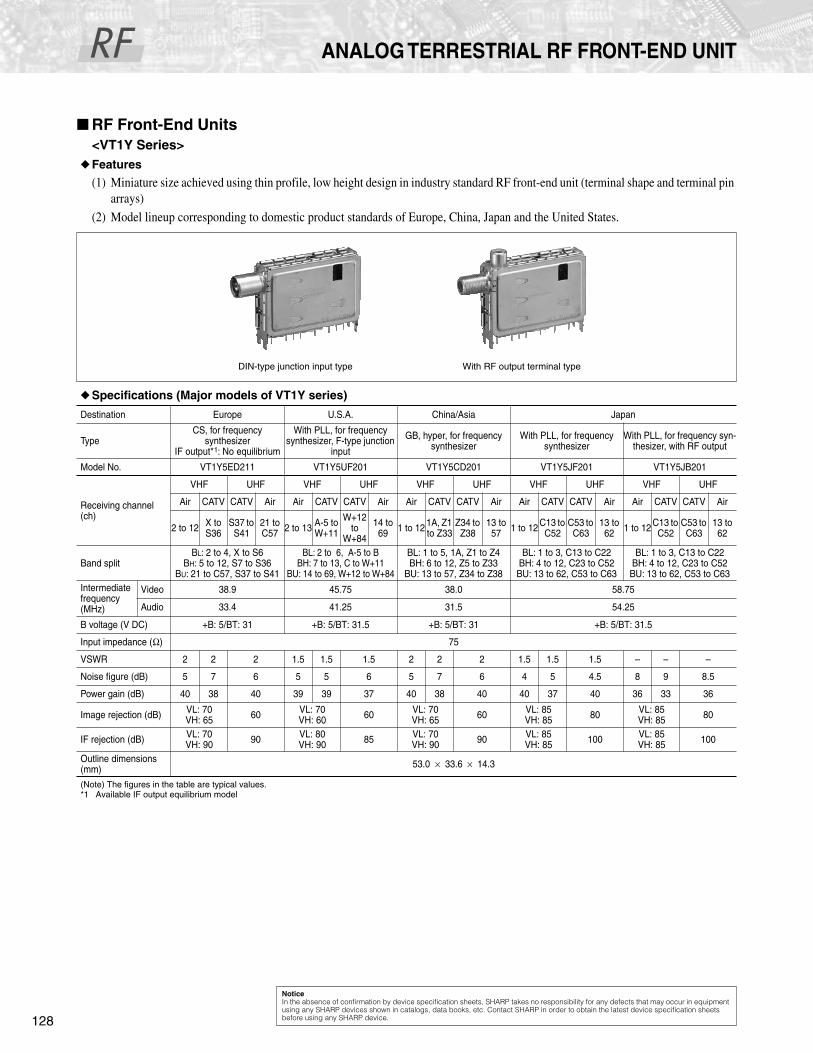
RF
128
ANALOG TERRESTRIAL RF FRONT-END UNIT
RF Front-End Units
<VT1Y Series>
Features
(1) Miniature size achieved using thin profile, low height design in industry standard RF front-end unit (terminal shape and terminal pin arrays)
(2) Model lineup corresponding to domestic product standards of Europe, China, Japan and the United States.
Specifications (Major models of VT1Y series)
(Note) The figures in the table are typical values.*1 Available IF output equilibrium model
DIN-type junction input type With RF output terminal type
Destination Europe U.S.A. China/Asia Japan
TypeCS, for frequency
synthesizerIF output*
1
: No equilibrium
With PLL, for frequency synthesizer, F-type junction
input
GB, hyper, for frequency synthesizer
With PLL, for frequency synthesizer
With PLL, for frequency syn-thesizer, with RF output
Model No. VT1Y5ED211 VT1Y5UF201 VT1Y5CD201 VT1Y5JF201 VT1Y5JB201
Receiving channel (ch)
VHF UHF VHF UHF VHF UHF VHF UHF VHF UHF
Air CATV CATV Air Air CATV CATV Air Air CATV CATV Air Air CATV CATV Air Air CATV CATV Air
2 to 12 X to S36
S37 to S41
21 to C57 2 to 13 A-5 to
W+11
W+12 to
W+84
14 to 69 1 to 12 1A, Z1
to Z33Z34 to
Z3813 to
57 1 to 12 C13 to C52
C53 to C63
13 to 62 1 to 12 C13 to
C52C53 to
C6313 to
62
Band splitB
L
: 2 to 4, X to S6B
H
: 5 to 12, S7 to S36B
U
: 21 to C57, S37 to S41
BL: 2 to 6, A-5 to BBH: 7 to 13, C to W+11
BU: 14 to 69, W+12 to W+84
BL: 1 to 5, 1A, Z1 to Z4BH: 6 to 12, Z5 to Z33
BU: 13 to 57, Z34 to Z38
BL: 1 to 3, C13 to C22BH: 4 to 12, C23 to C52BU: 13 to 62, C53 to C63
BL: 1 to 3, C13 to C22BH: 4 to 12, C23 to C52BU: 13 to 62, C53 to C63
Intermediate frequency (MHz)
Video 38.9 45.75 38.0 58.75
Audio 33.4 41.25 31.5 54.25
B voltage (V DC) +B: 5/BT: 31 +B: 5/BT: 31.5 +B: 5/BT: 31 +B: 5/BT: 31.5
Input impedance (
Ω
) 75
VSWR 2 2 2 1.5 1.5 1.5 2 2 2 1.5 1.5 1.5 – – –
Noise figure (dB) 5 7 6 5 5 6 5 7 6 4 5 4.5 8 9 8.5
Power gain (dB) 40 38 40 39 39 37 40 38 40 40 37 40 36 33 36
Image rejection (dB) VL: 70VH: 65 60 VL: 70
VH: 60 60 VL: 70VH: 65 60 VL: 85
VH: 85 80 VL: 85VH: 85 80
IF rejection (dB) VL: 70VH: 90 90 VL: 80
VH: 90 85 VL: 70VH: 90 90 VL: 85
VH: 85 100 VL: 85VH: 85 100
Outline dimensions (mm) 53.0
×
33.6
×
14.3
Notice
In the absence of confirmation by device specification sheets, SHARP takes no responsibility for any defects that may occur in equipment using any SHARP devices shown in catalogs, data books, etc. Contact SHARP in order to obtain the latest device specification sheets before using any SHARP device.

129
RF C
ompo
nent
s
MOBILE DIGITAL TERRESTRIAL MODULE
1-Segment Digital Terrestrial Module
Features
(1) High sensitivity: -109 dBm [typ.] (GPSK, CR1/2 ch13)
(2) Compact and thin design: 9.0 x 9.0 x 1.5 mm
(3) Low power consumption: 95 mW*
1
(4) Output interface: TS serial output
Standard Specifications
*1 Average value when current consumption is controlled by software*2 I
2
C-bus is a trademark of Philips Corporation.
1-segment/3-segment Digital Terrestrial Module
Features
(1) High sensitivity: -109 dBm [typ.] (QPSK, CR1/2 ch15)-110 dBm [typ.] (QPSK, CR1/2 ch7)
(2) Compact and thin design: 9.0 x 9.0 x 1.5 mm
(3) Low power consumption: 125 mW (at 3-segment), 120 mW (at 1-segment)
(4) Output interface: TS serial output
Standard Specifications
*1 I
2
C-bus is a trademark of Philips Corporation.
Destination Japan
Model No. VA35JZ9910
Input frequency 470 to 770 MHz (UHF: 13 to 62)
Input signal level -109 dBm [typ.] (GPSK, CR1/2)
Supply voltage2.9 V (RF)
1.5 V (OFDM Core)1.8 V to 2.9 V (I/O)
Power consumption 95 mW*
1
Operating temperature -20 to 85°C
Control I/F I
2
C-bus*
2
Power off function OFF for RF/OFDM power supply, 2 µA (MAX.) for I/O power supply (ON state)
Destination Japan
Model No. VA35JZ9904
Input frequency 188 to 198 MHz (UHF: 7, 8)470 to 770 MHz (UHF: 13 to 62)
Input signal level -109 dBm [typ.] (GPSK, CR1/2, ch7)-110 dBm [typ.] (GPSK, CR1/2, ch15)
Supply voltage1.8 V (RF)
1.2 V (OFDM Core)1.8 V to 2.8 V (I/O)
Power consumption 125 mW (at 3-segment), 120 mW (at 1-segment)
Operating temperature -20 to 85°C
Control I/F I
2
C-bus*
1
Power off function All power supplies can be OFF.
VA35JZ9910
VA35JZ9910
Notice
In the absence of confirmation by device specification sheets, SHARP takes no responsibility for any defects that may occur in equipment using any SHARP devices shown in catalogs, data books, etc. Contact SHARP in order to obtain the latest device specification sheets before using any SHARP device.
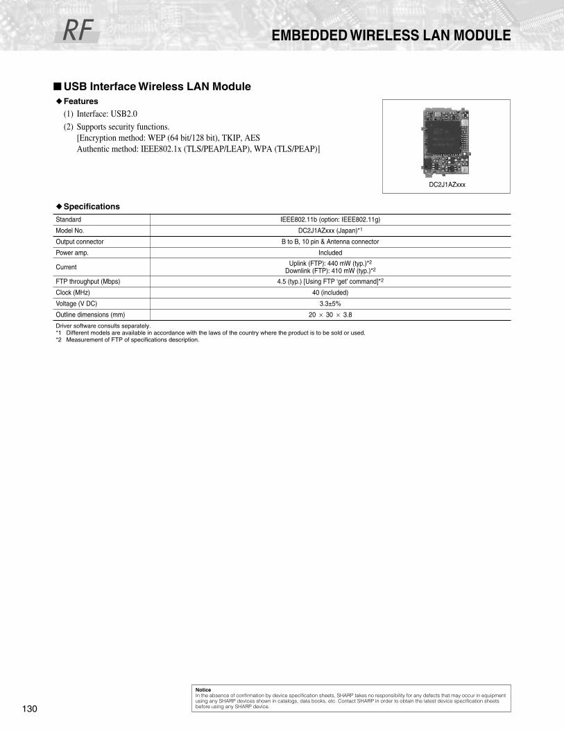
RF
130
EMBEDDED WIRELESS LAN MODULE
USB Interface Wireless LAN Module
Features
(1) Interface: USB2.0
(2) Supports security functions. [Encryption method: WEP (64 bit/128 bit), TKIP, AESAuthentic method: IEEE802.1x (TLS/PEAP/LEAP), WPA (TLS/PEAP)]
Specifications
Driver software consults separately.*1 Different models are available in accordance with the laws of the country where the product is to be sold or used.*2 Measurement of FTP of specifications description.
Standard IEEE802.11b (option: IEEE802.11g)
Model No. DC2J1AZxxx (Japan)*
1
Output connector B to B, 10 pin & Antenna connector
Power amp. Included
Current Uplink (FTP): 440 mW (typ.)*
2
Downlink (FTP): 410 mW (typ.)*
2
FTP throughput (Mbps) 4.5 (typ.) [Using FTP ‘get’ command]*
2
Clock (MHz) 40 (included)
Voltage (V DC) 3.3±5%
Outline dimensions (mm) 20
×
30
×
3.8
DC2J1AZxxx
Notice
In the absence of confirmation by device specification sheets, SHARP takes no responsibility for any defects that may occur in equipment using any SHARP devices shown in catalogs, data books, etc. Contact SHARP in order to obtain the latest device specification sheets before using any SHARP device.

IR
131
IR D
evic
e
INFRARED DATA COMMUNICATION DEVICE INDEX TREE
Infrared Data Communication Device Lineup
Infrared Wireless Audio Transmission Device Lineup
Communication system
Transmission speed
Transmission distance Features Operating
supply voltage Model No.
IrDA data FIR 4 Mb/s 100 cm
Compact, thin (height: 2.5 mm), low voltage operation type, LP/HP mode switching function 2.4 to 3.6 V GP2W1004YP0F
(IrDA 1.x)Compact 2.7 to 5.5 V GP2W1001YP0F
70 cm LP/HP mode switching function GP2W1010YP0F
50/20 cmLP/HP mode switching and remote control transmission functions GP2W3120YP0F
FIR LP 4 Mb/s 50/20 cm LP/HP mode switching function 2.7 to 3.6 V GP2W1320YP0F
FIR LP 4 Mb/s 70/20 cmLP/MP/HP mode switching and remote con-trol transmission functions 2.6 to 3.3 V GP2W3104YP0F
MIR 1.152 Mb/s 100 cm Compact, low dissipation current 2.4 to 3.6 V GP2W1002YP0F
70 cm 2.4 to 3.6 V GP2W1302YP0F
50 cm 2.4 to 3.6 V GP2W1304YP
SIR 115.2 kb/s 100 cm Compact, low dissipation current 2.4 to 5.5 VGP2W0004YP0F/GP2W0004XP0F
80 cmRemote control transmission function, compact, low dissipation current 2.4 to 5.5 V GP2W3020YP
SIR LP 115.2 kb/s 20 cmBuilt-in LED constant current circuit, 3-state output 2.0 to 3.6 V
GP2W0110VX/GP2W0110VY
Compact 2.0 to 3.6 V GP2W0116YP0F
(Height: 1.5 mm) 2.4 to 3.6 V GP2W0150YP0F
Built-in LED constant current circuit, 3-state output, top view type 2.0 to 3.6 V GP2W0114YP0F
Compact 2.0 to 3.6 V GP2W0118YP0F
(Height: 2.1 mm) 2.4 to 3.6 V GP2W0150XP0F
Built-in LED constant current circuit, 3-state output, low voltage operation type, low dissipation current type 1.8 to 2.5 V GP2W0112YP0F
Remote control transmission func-tion (built-in drive circuit)
λ
p: 870, 940 nm 2.4 to 3.6 V GP2W3240YP
λ
p: 890 nm 2.4 to 3.6 V GP2W3250YP
(Height: 1.5 mm) 2.4 to 3.6 V GP2W3270YP0F
Top view type 2.4 to 3.6 V GP2W3270XP0F
Communication system Features Operating supply voltage Model No.
Infrared system (1-bit audio transmission)
For designing compact, low-power-consumption audio transmission systems 2.4 to 3.6 V
GP2WVR01YP0F/GP2WVC01MP0F (Transmission LSI)
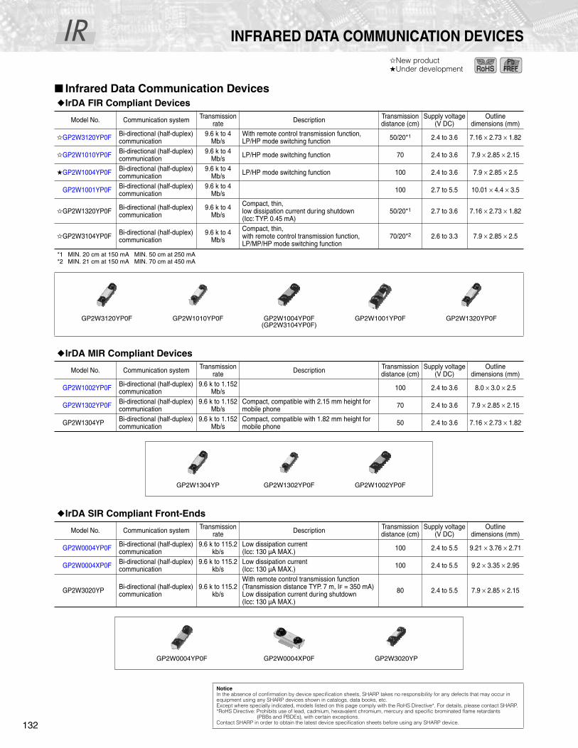
IR
132
INFRARED DATA COMMUNICATION DEVICES
New product
Under development
Infrared Data Communication Devices
IrDA FIR Compliant Devices
*1 MIN. 20 cm at 150 mA MIN. 50 cm at 250 mA*2 MIN. 21 cm at 150 mA MIN. 70 cm at 450 mA
IrDA MIR Compliant Devices
IrDA SIR Compliant Front-Ends
Model No. Communication system Transmission rate Description Transmission
distance (cm)Supply voltage
(V DC)Outline
dimensions (mm)
GP2W3120YP0F Bi-directional (half-duplex) communication
9.6 k to 4 Mb/s
With remote control transmission function, LP/HP mode switching function 50/20*
1
2.4 to 3.6 7.16
×
2.73
×
1.82
GP2W1010YP0F Bi-directional (half-duplex) communication
9.6 k to 4 Mb/s LP/HP mode switching function 70 2.4 to 3.6 7.9
×
2.85
×
2.15
GP2W1004YP0F Bi-directional (half-duplex) communication
9.6 k to 4 Mb/s LP/HP mode switching function 100 2.4 to 3.6 7.9
×
2.85
×
2.5
GP2W1001YP0F Bi-directional (half-duplex) communication
9.6 k to 4 Mb/s 100 2.7 to 5.5 10.01
×
4.4
×
3.5
GP2W1320YP0F Bi-directional (half-duplex) communication
9.6 k to 4 Mb/s
Compact, thin, low dissipation current during shutdown (Icc: TYP. 0.45 mA)
50/20*
1
2.7 to 3.6 7.16
×
2.73
×
1.82
GP2W3104YP0F Bi-directional (half-duplex) communication
9.6 k to 4 Mb/s
Compact, thin, with remote control transmission function, LP/MP/HP mode switching function
70/20*
2
2.6 to 3.3 7.9
×
2.85
×
2.5
GP2W3120YP0F GP2W1010YP0F GP2W1004YP0F(GP2W3104YP0F)
GP2W1001YP0F GP2W1320YP0F
Model No. Communication system Transmission rate Description Transmission
distance (cm)Supply voltage
(V DC)Outline
dimensions (mm)
GP2W1002YP0F Bi-directional (half-duplex) communication
9.6 k to 1.152 Mb/s 100 2.4 to 3.6 8.0
×
3.0
×
2.5
GP2W1302YP0F Bi-directional (half-duplex) communication
9.6 k to 1.152 Mb/s
Compact, compatible with 2.15 mm height for mobile phone 70 2.4 to 3.6 7.9
×
2.85
×
2.15
GP2W1304YP Bi-directional (half-duplex) communication
9.6 k to 1.152 Mb/s
Compact, compatible with 1.82 mm height for mobile phone 50 2.4 to 3.6 7.16
×
2.73
×
1.82
GP2W1304YP GP2W1302YP0F GP2W1002YP0F
Model No. Communication system Transmission rate Description Transmission
distance (cm)Supply voltage
(V DC)Outline
dimensions (mm)
GP2W0004YP0F Bi-directional (half-duplex) communication
9.6 k to 115.2 kb/s
Low dissipation current (Icc: 130 µA MAX.) 100 2.4 to 5.5 9.21
×
3.76
×
2.71
GP2W0004XP0F Bi-directional (half-duplex) communication
9.6 k to 115.2 kb/s
Low dissipation current (Icc: 130 µA MAX.) 100 2.4 to 5.5 9.2
×
3.35
×
2.95
GP2W3020YP Bi-directional (half-duplex) communication
9.6 k to 115.2 kb/s
With remote control transmission function(Transmission distance TYP. 7 m, I
F
= 350 mA)Low dissipation current during shutdown (Icc: 130 µA MAX.)
80 2.4 to 5.5 7.9
×
2.85
×
2.15
GP2W0004YP0F GP2W0004XP0F GP2W3020YP
Notice
In the absence of confirmation by device specification sheets, SHARP takes no responsibility for any defects that may occur in equipment using any SHARP devices shown in catalogs, data books, etc. Except where specially indicated, models listed on this page comply with the RoHS Directive*. For details, please contact SHARP.*RoHS Directive: Prohibits use of lead, cadmium, hexavalent chromium, mercury and specific brominated flame retardants (PBBs and PBDEs), with certain exceptions.Contact SHARP in order to obtain the latest device specification sheets before using any SHARP device.

133
IR D
evic
e
INFRARED DATA COMMUNICATION DEVICE
IrDA SIR LP Compliant Front-Ends
The model marked with
may not be available in the near future. Contact with SHARP for details before use.
Infrared Wireless Audio Transmission Device
Model No. Communication system Transmission rate Description Transmission
distance (cm)Supply voltage
(V DC)Outline
dimensions (mm)
GP2W0110VX/VY Bi-directional (half-duplex) communication
2.4 k to 115.2 kb/s
Top-view and side view compatible (Model name is prescribed based on the packaging status.), lead-free type available
20 2.0 to 3.6 6.8
×
2.35
×
2.1
GP2W0112YP0F
Bi-directional (half-duplex) communication
2.4 k to 115.2 kb/s
Low voltage operation, low dissipation current, 3-state output type, independent power supply for light-emitting and light-detecting circuits
20 1.7 to 2.5 7.9
×
2.85
×
2.15
GP2W0150YP0F Bi-directional (half-duplex) communication
2.4 k to 115.2 kb/s
Compact, thin, low dissipation current (Icc: 100 µA MAX.) 20 2.4 to 3.6 7.6
×
2.4
×
1.5
GP2W0150XP0F Bi-directional (half-duplex) communication
2.4 k to 115.2 kb/s
Compact, thin, low dissipation current (Icc: 100 µA MAX.)Top view type
20 2.4 to 3.6 8.3
×
2.1
×
1.7
GP2W0116YP0F
Bi-directional (half-duplex) communication
2.4 k to 115.2 kb/s
Compact, thin, low dissipation current (Icc: 120 µA MAX.) 20 2.0 to 3.6 7.2
×
2.75
×
1.85
GP2W0118YP0F
Bi-directional (half-duplex) communication
2.4 k to 115.2 kb/s
Compact, thin, low dissipation current (Icc: 120 µA MAX.)Top view type
20 2.0 to 3.6 7.9
×
2.25
×
2.0
GP2W3240YP
Bi-directional (half-duplex) communication
2.4 k to 115.2 kb/s
With remote control transmit function (with remote control drive circuit) (
λ
p = 940 nm)IR communication part (
λ
p = 870 nm)20 2.4 to 3.6 8.6
×
2.85
×
1.85
GP2W3250YP Bi-directional (half-duplex) communication
2.4 k to 115.2 kb/s
Remote control transmission function, shared IR communication section (
λ
p = 890 nm) 20 2.4 to 3.6 7.2
×
2.55
×
1.85
GP2W3270YP0F Bi-directional (half-duplex) communication
2.4 k to 115.2 kb/s
Remote control transmission function, shared IR communication section (
λ
p = 890 nm) 20 2.4 to 3.6 7.6
×
2.4
×
1.5
GP2W3270XP0F Bi-directional (half-duplex) communication
2.4 k to 115.2 kb/s
Remote control transmission function, shared IR communication section (
λ
p = 890 nm)Top view type
20 2.4 to 3.6 8.3
×
2.1
×
1.7
GP2W0110VX(GP2W0110VY)
GP2W0112YP0F GP2W0150YP0F(GP2W3270YP0F)
GP2W0150XP0F(GP2W3270XP0F)
GP2W0116YP0F GP2W0118YP0F GP2W3240YP GP2W3250YP
Model No. Communication system Features S/N ratio Supply voltage (V DC)
Outline dimensions (mm)
GP2WVR01YP0F (Reception Device)
1-bit audio transmission (1.5 MHz)
Compact, low power consumption typeSimple circuit configuration: Used in combination with transmission LSI (GP2WVC01MP0F) and transmission device (GP2W1004YP0F, etc.)
70 dB 2.4 to 3.6 2.5
×
8
×
3
GP2WVR01YP0F
Notice
In the absence of confirmation by device specification sheets, SHARP takes no responsibility for any defects that may occur in equipment using any SHARP devices shown in catalogs, data books, etc. Except where specially indicated, models listed on this page comply with the RoHS Directive*. For details, please contact SHARP.*RoHS Directive: Prohibits use of lead, cadmium, hexavalent chromium, mercury and specific brominated flame retardants (PBBs and PBDEs), with certain exceptions.Contact SHARP in order to obtain the latest device specification sheets before using any SHARP device.
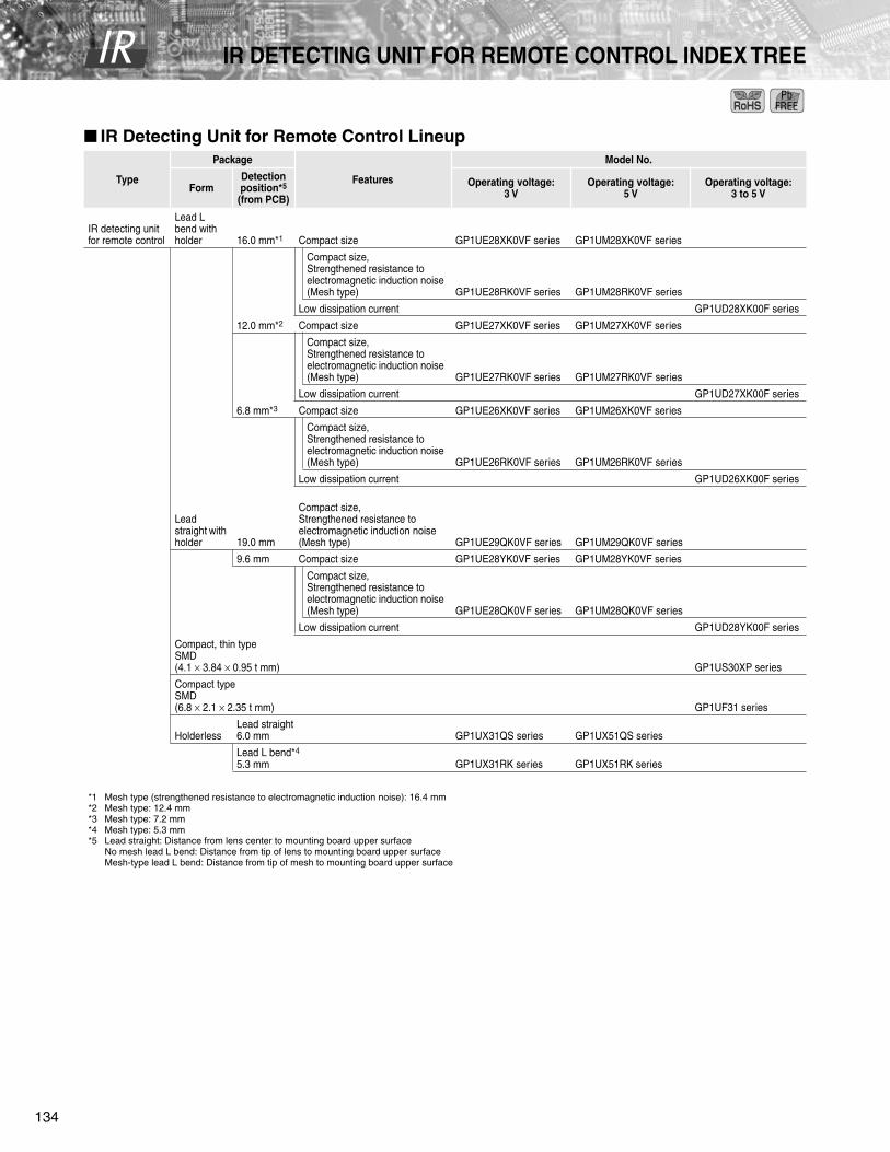
IR
134
IR DETECTING UNIT FOR REMOTE CONTROL INDEX TREE
IR Detecting Unit for Remote Control Lineup
*1 Mesh type (strengthened resistance to electromagnetic induction noise): 16.4 mm*2 Mesh type: 12.4 mm*3 Mesh type: 7.2 mm*4 Mesh type: 5.3 mm*5 Lead straight: Distance from lens center to mounting board upper surface
No mesh lead L bend: Distance from tip of lens to mounting board upper surfaceMesh-type lead L bend: Distance from tip of mesh to mounting board upper surface
Type
Package
Features
Model No.
FormDetection position*
5
(from PCB)
Operating voltage: 3 V
Operating voltage: 5 V
Operating voltage: 3 to 5 V
IR detecting unitfor remote control
Lead L bend with holder 16.0 mm*
1
Compact size GP1UE28XK0VF series GP1UM28XK0VF series
Compact size, Strengthened resistance toelectromagnetic induction noise (Mesh type) GP1UE28RK0VF series GP1UM28RK0VF series
Low dissipation current GP1UD28XK00F series
12.0 mm*
2
Compact size GP1UE27XK0VF series GP1UM27XK0VF series
Compact size, Strengthened resistance toelectromagnetic induction noise (Mesh type) GP1UE27RK0VF series GP1UM27RK0VF series
Low dissipation current GP1UD27XK00F series
6.8 mm*
3
Compact size GP1UE26XK0VF series GP1UM26XK0VF series
Compact size, Strengthened resistance toelectromagnetic induction noise (Mesh type) GP1UE26RK0VF series GP1UM26RK0VF series
Low dissipation current GP1UD26XK00F series
Lead straight with holder 19.0 mm
Compact size, Strengthened resistance toelectromagnetic induction noise (Mesh type) GP1UE29QK0VF series GP1UM29QK0VF series
9.6 mm Compact size GP1UE28YK0VF series GP1UM28YK0VF series
Compact size, Strengthened resistance toelectromagnetic induction noise (Mesh type) GP1UE28QK0VF series GP1UM28QK0VF series
Low dissipation current GP1UD28YK00F series
Compact, thin typeSMD (4.1
×
3.84
×
0.95 t mm) GP1US30XP series
Compact typeSMD (6.8
×
2.1
×
2.35 t mm) GP1UF31 series
HolderlessLead straight 6.0 mm GP1UX31QS series GP1UX51QS series
Lead L bend*
4
5.3 mm GP1UX31RK series GP1UX51RK series
!

135
IR D
evic
e
IR DETECTING UNIT FOR REMOTE CONTROL
New product
IR Detecting Units for Remote Control
*1 When no signal is input (during input light).*2 Figures in parentheses indicate the distance to the light detection center.*3 In addition to the fo = 40kHz type, types fo = 36, 38, 36.7, 56.8, 32.75 kHz are also available.*4 Type with strengthened resistance to electromagnetic induction noise.*5 A voltage regulator circuit is built-in but may be affected by the usage environment. Install with an externally mounted
C and R as a power supply filter.*6 Allows reflow soldering.*7 Operating voltage: 2.4 to 3.6 V (2.7 to 3.6 V for fo = 56.8 kHz type)*8 Operating voltage: 2.7 to 5.5 V*9 Distance to transmitter on optical axis is 0.2 to 10.0 m. Ev < 10 lx when burst wave is input as shown in the right figure.*10 Distance to transmitter on optical axis is 0.2 to 10.0 m. Ev < 10 lx when burst wave is input as shown in the right figure.
(fo = 56.8 kHz: 0.2 to 9.0 m)*11 Distance to transmitter on optical axis is 0.2 to 8.5 m. Ev < 10 lx when burst wave is input as shown in the right figure.
(fo = 56.8 kHz: 0.2 to 7.0 m, fo = 32.75 kHz: 0.2 to 6.5 m)*12 GP1UM series operating voltage: 4.5 to 5.5 V*13 Operating voltage: 4.5 to 5.5 V*14 Distance to transmitter on optical axis is 0.2 to 8.0 m. Ev < 10 lx when burst wave is input as shown in the right figure.*15 Distance to transmitter on optical axis is 0.2 to 6.5 m. Ev < 10 lx when burst wave is input as shown in the right figure.*16 Types fo = 32.75, 36, 36.7, and 38 kHz are also available.*17 Operating voltage: 2.4 to 5.5 V*18 fo = 56.8 kHz*19 Distance to transmitter on optical axis is 0.2 to 5.0 m. Ev < 10 lx when burst wave is input as shown in the right figure.*20 In addition to the fo = 40 kHz type, types fo = 36, 36.7, and 38 kHz are also available.
Series No.
Absolute maximum ratings Electrical characteristics
Size (mm) RemarksVcc (V) Topr (°C)
Icc (mA)
*1
MAX.
V
OH
(V) MIN.
V
OL
(V) MAX.
fo (kHz) TYP.
GP1UM26XK0VF*
12
0 to 6.0 –10 to +70 0.6 (0.65)*
18
Vcc–0.5*
10
0.45*
10
40*
3
5.6
×
9.6
×
6.8 *
5
GP1UM27XK0VF*
12
0 to 6.0 –10 to +70 0.6 (0.65)*
18
Vcc–0.5*
10
0.45*
10
40*
3
5.6
×
9.6
×
12.0 *
5
GP1UM28XK0VF*
12
0 to 6.0 –10 to +70 0.6 (0.65)*
18
Vcc–0.5*
10
0.45*
10
40*
3
5.6
×
9.6
×
16.0 *
5
GP1UM28YK0VF*
12
0 to 6.0 –10 to +70 0.6 (0.65)*
18
Vcc–0.5*
10
0.45*
10
40*
3
5.6
×
8.6
×
12.5(9.6)*
2
*
5
GP1UM26RK0VF*
4, 12
0 to 6.0 –10 to +70 0.6 (0.65)*
18
Vcc–0.5*
11
0.45*
11
40*
3
5.6
×
9.6
×
7.2 *
5
GP1UM27RK0VF*
4, 12
0 to 6.0 –10 to +70 0.6 (0.65)*
18
Vcc–0.5*
11
0.45*
11
40*
3
5.6
×
9.6
×
12.4 *
5
GP1UM28RK0VF*
4, 12
0 to 6.0 –10 to +70 0.6 (0.65)*
18
Vcc–0.5*
11
0.45*
11
40*
3
5.6
×
9.6
×
16.4 *
5
GP1UM28QK0VF*
4, 12
0 to 6.0 –10 to +70 0.6 (0.65)*
18
Vcc–0.5*
11
0.45*
11
40*
3
5.6
×
9.0
×
12.5(9.6)*
2
*
5
GP1UM29QK0VF*
4, 12
0 to 6.0 –10 to +70 0.6 (0.65)*
18
Vcc–0.5*
11
0.45*
11
40*
3
5.6
×
16.2
×
21.9(19)*
2
*
5
GP1UE26XK0VF*
8
0 to 6.0 –10 to +70 0.4 Vcc–0.5*
9
0.45*
9
40*
16
5.6
×
9.6
×
6.8 *
5
GP1UE27XK0VF*
8
0 to 6.0 –10 to +70 0.4 Vcc–0.5*
9
0.45*
9
40*
16
5.6
×
9.6
×
12.0 *
5
GP1UE28XK0VF*
8
0 to 6.0 –10 to +70 0.4 Vcc–0.5*
9
0.45*
9
40*
16
5.6
×
9.6
×
16.0 *
5
GP1UE28YK0VF*
8
0 to 6.0 –10 to +70 0.4 Vcc–0.5*
9
0.45*
9
40*
16
5.6
×
8.6
×
12.5(9.6)*
2
*
5
GP1UE26RK0VF*
8
0 to 6.0 –10 to +70 0.4 Vcc–0.5*
14
0.45*
14
40*
16
5.6
×
9.6
×
7.2 *
5
GP1UE27RK0VF*
8
0 to 6.0 –10 to +70 0.4 Vcc–0.5*
14
0.45*
14
40*16 5.6 × 9.6 × 12.4 *5
GP1UE28RK0VF*8 0 to 6.0 –10 to +70 0.4 Vcc–0.5*14 0.45*14 40*16 5.6 × 9.6 × 16.4 *5
GP1UE28QK0VF*8 0 to 6.0 –10 to +70 0.4 Vcc–0.5*14 0.45*14 40*16 5.6 × 9.0 × 12.5(9.6)*2 *5
GP1UE29QK0VF*8 0 to 6.0 –10 to +70 0.4 Vcc–0.5*14 0.45*14 40*16 5.6 × 16.2 × 21.9(19)*2 *5
GP1UD26XK00F*8 0 to 6.0 –10 to +70 0.2 (Vcc = 3 V) Vcc–0.5*9 0.5*9 40*3 7.3 × 13.1 × 6.8 *5
GP1UD27XK00F*8 0 to 6.0 –10 to +70 0.2 (Vcc = 3 V) Vcc–0.5*9 0.5*9 40*3 7.3 × 13.1 × 12.0 *5
GP1UD28XK00F*8 0 to 6.0 –10 to +70 0.2 (Vcc = 3 V) Vcc–0.5*9 0.5*9 40*3 7.3 × 13.1 × 16.0 *5
GP1UD28YK00F*8 0 to 6.0 –10 to +70 0.2 (Vcc = 3 V) Vcc–0.5*9 0.5*9 40*3 7.3 × 8.4 × 13.0(9.6)*2 *5
GP1UV70QS00F*13 – –10 to +70 1.5 Vcc–0.5*11 0.45*11 40*3 5.6 × 6.2 × 7.6(6.0)*2 *5, Pin configuration (Pin No. 2: GND)
GP1UW70QS00F*7 – –10 to +70 0.6 Vcc–0.5 0.45 40*3 5.6 × 6.2 × 7.6(6.0)*2 *5, Pin configuration (Pin No. 2: GND)
GP1UX51QS*13 0 to 6.0 –10 to +70 0.6 Vcc–0.5*11 0.45*11 40*16 5.5 × 5.3 × 7.5 *5, Pin configuration (Pin No. 2: GND)
GP1UX51RK*13 0 to 6.0 –10 to +70 1.5 Vcc–0.5 0.45 40*3 5.5 × 5.3 × 7.5 *5, Pin configuration (Pin No. 2: GND), Folded lead
GP1UX31QS*7, *8 0 to 6.0 –10 to +70 0.4 Vcc–0.5*14 0.45*14 40 5.5 × 5.3 × 7.5 *5, Pin configuration (Pin No. 2: GND)
GP1UX31RK*8 0 to 6.0 –10 to +70 0.4 Vcc–0.5*14 0.45*14 40 5.5 × 5.3 × 7.5 *5, Pin configuration (Pin No. 2: GND), Folded lead
GP1US30XP*6, 17 – –30 to +85 0.6 Vcc–0.5*11 0.45*19 40 4.1 × 3.95 × 0.95 *5, Surface mount compatibleGP1UF31xXP0F 0 to 6.0 –30 to +85 0.4 Vcc–0.5 0.45 40*20 6.8 × 2.1 × 2.0 *5, Surface mount compatibleGP1UF31xYP0F 0 to 6.0 –30 to +85 0.4 Vcc–0.5 0.45 40*20 6.8 × 2.1 × 2.0 *5, Surface mount compatible
(Ta = 25°C)
Duty = 50%1 000 µs600 µs
<Burst wave>
GP1UD series, GP1UM series, GP1UE series have different fo values for each model.
NoticeIn the absence of confirmation by device specification sheets, SHARP takes no responsibility for any defects that may occur in equipment using any SHARP devices shown in catalogs, data books, etc. Except where specially indicated, models listed on this page comply with the RoHS Directive*. For details, please contact SHARP.*RoHS Directive: Prohibits use of lead, cadmium, hexavalent chromium, mercury and specific brominated flame retardants (PBBs and PBDEs), with certain exceptions.Contact SHARP in order to obtain the latest device specification sheets before using any SHARP device.
"
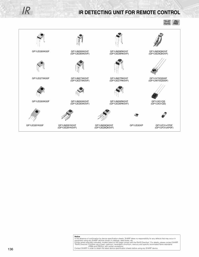
IR
136
IR DETECTING UNIT FOR REMOTE CONTROL
GP1UD28XK00F GP1UM28XK0VF(GP1UE28XK0VF)
GP1UM28RK0VF(GP1UE28RK0VF)
GP1UM29QK0VF(GP1UE29QK0VF)
GP1UD27XK00F GP1UM27XK0VF(GP1UE27XK0VF)
GP1UM27RK0VF(GP1UE27RK0VF)
GP1UV70QS00F(GP1UW70QS00F)
GP1UD26XK00F GP1UM26XK0VF(GP1UE26XK0VF)
GP1UM26RK0VF(GP1UE26RK0VF)
GP1UX51QS(GP1UX31QS)
GP1UD28YK00F GP1UM28YK0VF(GP1UE28YK0VF)
GP1UM28QK0VF(GP1UE28QK0VF)
GP1US30XP GP1UF31xYP0F(GP1UF31xXP0F)
Notice
In the absence of confirmation by device specification sheets, SHARP takes no responsibility for any defects that may occur in equipment using any SHARP devices shown in catalogs, data books, etc. Except where specially indicated, models listed on this page comply with the RoHS Directive*. For details, please contact SHARP.*RoHS Directive: Prohibits use of lead, cadmium, hexavalent chromium, mercury and specific brominated flame retardants (PBBs and PBDEs), with certain exceptions.Contact SHARP in order to obtain the latest device specification sheets before using any SHARP device.
#

POWER
137
Pow
er S
uppl
y De
vice
SWITCHING POWER SUPPLY
Switching Power Supplies (Custom)
Features
(1) Satisfies energy saving regulations thanks to the high conversion efficiency
(2) Compact and high reliability thanks to the modulated main switching and chopper circuits
(3) EMI filter built-in, low noise design
(4) Environmentally safe types are also available. [RoHS, lead-free]
Specification examples
* Types with input voltage of AC 100 V, 120 V, 200 V are also available. Types with other specification are also available upon request.For LCD TVs (20
′′
to 22
′′
), an integrated power source with an inverter circuit for backlights is also available.
Switching Power Supply with Integrated High/Low Voltage Circuit (Custom)
Features
(1) Realizes compact and low cost thanks to the integrated high/low voltage circuit
(2) Easy connection between high voltage and low voltage circuits
(3) Highly efficiency energy saving power supply at standby mode can be installed for low voltage circuit
(4) Environmentally safe types are also available. [RoHS, lead-free]
Specifications
Applications LCD TV (20 to 22
′′
)LCD TV
(26 to 32
′′
)Laser-beam printer/
Scanner/FAXInput voltage (V AC) 90 to 110 90 to 264 85 to 138Input frequency (Hz) 50/60 50/60 50/60
Output voltage (V)(Current capacity)
+24 (1.9 A) +12 (3.5 A)
+24 (5.0 A) +12 (4.0 A) +5 (5.5 A) +5 (1.5 A)
+3.3 (3.0 A)
+3.3 (0.25 A) +5 (1.1 A)
+12 (0.13 A)+24 (2.0 A)
Rated output power (W) 87.6 213 55.9
Stand-by power loss (W) 0.3 (without load) 0.1 –
Protection circuit Overcurrent and overvoltage protectionConfiguration On-boardOutline dimensions (mm) 118
×
208
×
36 140
×
244
×
35.6 204
×
124
×
40
Sharp ‘Green Power Supply’ adapting with integrated high/low voltage circuit regulation
High voltage
Switching power supply system Pulse width control or RCC methodInput voltage (V DC) 24Output voltage (kV DC) +5.5 (+280 µA)/-5.5 (-560 µA), etc.
Low voltage
Switching power supply system Pulse width control or RCC methodInput voltage (V AC) 100, 120, 230Power capacity (W) 184
Notice
In the absence of confirmation by device specification sheets, SHARP takes no responsibility for any defects that may occur in equipment using any SHARP devices shown in catalogs, data books, etc. Contact SHARP in order to obtain the latest device specification sheets before using any SHARP device.

PCB
138
PRINTED CIRCUIT BOARDS
Advanced Flex Printed Circuit Boards
he advanced flex printed circuit board is a multilayered composite wiring board comprised of flexible printed circuits (FPC) laminated into a multilayer configuration. The PWBs and FPCs are connected to each other via copper-plated through holes. It is
ideal for compact, light-weight equipment design.
Features
(1) For selecting optimal specifications to suit specific applications, special specifications such as for mobile phones are available. • Minimum thickness in multi-layer part: 0.26 mm (4-layer), 0.33 mm (6-layer) • Minimum pattern width/pitch: 0.06/0.07 mm • Flexibility of single/double sided FPC part (dedicated for hinge): More than 200 000 times 180-degree bending of radius 3 mm
(2) Capable of board-to-board connection without connectors, which enables space-saving and 3-dimensional equipment assembly.
(3) Through hole plating connection of multi-layer (3 to 8) part to flexible part significantly improves reliability.
(4) Blind Via Hole (BVH) forming with laser via drilling of small diameter.
(5) Sheet design provides excellent mountablity, equivalent to that of PWB.
Outline Specifications
Type Folding type/Flying tail type
Min. base thickness 0.26 mm (4-layer), 0.33 mm (6-layer), 0.40 mm (8-layer)
Min. line width/spacing 0.06/0.07 mmMin. through hole diameter ø0.25 mm
Min. via hole land diameter
Through hole Outer layer: ø0.5 mm, Inner layer: ø0.5 mm
Blind via hole ø0.09 mm
Inner via hole ø0.30 mm
Solder resist Multi layer: Liquid photo solder resist, FPC: Film cover ray
Surface finish Heat-resistant preflux, Ni-Au plating (Ni-Au plating for flying tail)
Safety standard (UL approval) 94V-0
T
Construction of Advanced Flex Board (6-layer sample)
Laser via hole (BVH)
Through hole
PP
FPC
FPC
PP
FPC
Notice
In the absence of confirmation by device specification sheets, SHARP takes no responsibility for any defects that may occur in equipment using any SHARP devices shown in catalogs, data books, etc. Contact SHARP in order to obtain the latest device specification sheets before using any SHARP device.
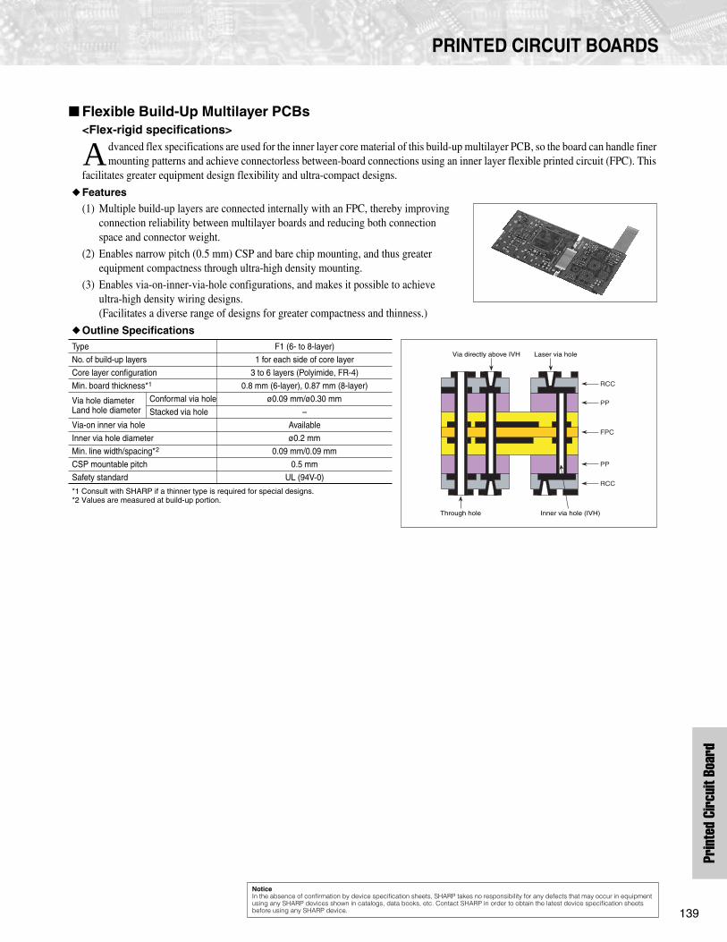
139
Prin
ted
Circ
uit B
oard
PRINTED CIRCUIT BOARDS
Flexible Build-Up Multilayer PCBs
<Flex-rigid specifications>
dvanced flex specifications are used for the inner layer core material of this build-up multilayer PCB, so the board can handle finer mounting patterns and achieve connectorless between-board connections using an inner layer flexible printed circuit (FPC). This
facilitates greater equipment design flexibility and ultra-compact designs.
Features
(1) Multiple build-up layers are connected internally with an FPC, thereby improving connection reliability between multilayer boards and reducing both connection space and connector weight.
(2) Enables narrow pitch (0.5 mm) CSP and bare chip mounting, and thus greater equipment compactness through ultra-high density mounting.
(3) Enables via-on-inner-via-hole configurations, and makes it possible to achieve ultra-high density wiring designs.(Facilitates a diverse range of designs for greater compactness and thinness.)
Outline Specifications
*1 Consult with SHARP if a thinner type is required for special designs.*2 Values are measured at build-up portion.
Type F1 (6- to 8-layer)
No. of build-up layers 1 for each side of core layer
Core layer configuration 3 to 6 layers (Polyimide, FR-4)
Min. board thickness*
1
0.8 mm (6-layer), 0.87 mm (8-layer)
Via hole diameterLand hole diameter
Conformal via hole ø0.09 mm/ø0.30 mm
Stacked via hole –
Via-on inner via hole Available
Inner via hole diameter ø0.2 mm
Min. line width/spacing*
2
0.09 mm/0.09 mm
CSP mountable pitch 0.5 mm
Safety standard UL (94V-0)
A
Laser via holeVia directly above IVH
Through hole Inner via hole (IVH)
PP
FPC
RCC
PP
RCC
Notice
In the absence of confirmation by device specification sheets, SHARP takes no responsibility for any defects that may occur in equipment using any SHARP devices shown in catalogs, data books, etc. Contact SHARP in order to obtain the latest device specification sheets before using any SHARP device.

PCB
140
PRINTED CIRCUIT BOARDS
Flexible Printed Circuit Boards
he flexible printed circuit board is designed for high space efficiency and product design flexibility, which are now aiming at more compact and higher density mounting. It also contributes to the reduction of assembly process and to the enhancement of the
reliability.
Features
(1) High density mounting circuit, SMT and other most suitable flexible PCB are available.
(2) High precision type for COF with flip chip mounting and wire bonding capabilities and other connector mounting type are available.
Standard specifications
Line-up Other line-up
Number of layers One side Both-side through-hole
Substrate materials Polyimido film, non-adhesive polyimido
Design pattern width 0.02 mm (MIN.) 0.05 mm (MIN.)
Design pattern spacing 0.04 mm (MIN.) 0.05 mm (MIN.)
Through-hole / land diameter – ø0.1 mm / ø0.3 mm (MIN.)
Cover lay Polyimido film, heat resistant ink, liquid soldering resist
Safety standard UL (94V-0)
Multi-layer flexible PCB Both-side flexible PCB Bonding Ni-Au plating
Single-layer flexible PCB Flex-rigid PCB Highly flexible (bending capacity)
Single-side high precision flexible PCB Both-side high precision flexible PCB High density SMT
T
Notice
In the absence of confirmation by device specification sheets, SHARP takes no responsibility for any defects that may occur in equipment using any SHARP devices shown in catalogs, data books, etc. Contact SHARP in order to obtain the latest device specification sheets before using any SHARP device.
!

UNIT
141
Unit
PICKUP
Slim Combo Drive Pickup<DD-56>
Features
Thin type pickup compatible with half-inch-height drive (12.7 mm thickness)
Playback speed:
×
8 (DVD-ROM),
×
24 (CD-ROM)
Recording speed:
×
24 (CD-R),
×
24 (CD-RW)
DVD-RAM readable
Outline dimensions: W 38.6
×
H 7.3
×
D 48.7 (mm)
Weight: Approx. 15 g
Slim DVD-ROM Drive Pickup<DD-30>
Features
Thin type pickup compatible with half-inch-height drive (12.7 mm thickness)
Playable disk: DVD-ROM/RAM, CD-ROM
Playback speed:
×
8 (DVD-ROM),
×
24 (CD-ROM)
Outline dimensions: W 38.7
×
H 7.3
×
D 48.7 (mm)
Weight: Approx. 8 g
DVD Pickup for Automotive Use<HPD-66>
Features
Compact, thin (7.3 mm) pickup
Playable disk: DVD-ROM, CD-ROM
Operating temperature: –30 to +85°C
Outline dimensions: W 30.2
×
H 7.3
×
D 48.7 (mm)
Notice
In the absence of confirmation by device specification sheets, SHARP takes no responsibility for any defects that may occur in equipment using any SHARP devices shown in catalogs, data books, etc. Contact SHARP in order to obtain the latest device specification sheets before using any SHARP device.
!

INDEX
142
INDEX
BS
BS1C1UR100A............................... 121
BS1F6JP100A ................................ 122
BS1F6JP300A ................................ 122
BS1F6JU300A................................ 122
BS1R8AR100A............................... 122
BS1R8EL100A ............................... 121
BS1R8EL200A ............................... 121
BS1R8EL400A ............................... 121
BS1R8EL500A ............................... 121
BS2F7HZ6460................................ 124
BS2F7VZ0165 ................................ 124
BS2F7VZ0460 ................................ 124
BS2F7VZ7395 ................................ 124
BS2S7HZ0502................................ 123
BS2S7HZ6306................................ 123
BS520E0F ........................................ 94
DC
DC2J1AZxxx................................... 130
DD
DD-30 ............................................. 141
DD-56 ............................................. 141
GA
GA104T1M1MZ ................................ 99
GA1A1S201WP................................ 97
GA1A2S100LY.................................. 97
GA1A2S100SS................................. 97
GA202TXV15J.................................. 98
GA202TXV15K ................................. 98
GA210TXV8SY................................. 98
GA220T2L1IZ ................................... 96
GA230TXR1ZY................................. 98
GA230TXW6SY................................ 98
GA250T6C3SY................................. 98
GA250T6C4SY................................. 98
GA301TXW5MZ ............................... 98
GH0
GH04020A2GE............................... 120
GH06P24A2C................................. 120
GH07805C2K ................................. 120
GH07825C2K ................................. 120
GH07P24C1C................................. 120
GH07P24C4C................................. 120
GH07P28A1C................................. 120
GH07P28A4C................................. 120
GH1
GH16P24A8C ................................. 120
GH16P30A8C ................................. 120
GH16P35A8C ................................. 120
GH17805B2AS ............................... 120
GH17P24C8C................................. 120
GH17P28A8C ................................. 120
GL0
GL0ZJ042B0S ................................ 111
GL0ZS042B0S................................ 111
GL0ZV042B0S................................ 111
GL1
GL100MD1MP1 .............................. 101
GL100MN0MP ................................ 101
GL100MN1MP ................................ 101
GL100MN3MP ................................ 101
GL2
GL2EG6.......................................... 113
GL2HD6.......................................... 113
GL2HY6 .......................................... 113
GL2PR6 .......................................... 113
GL3
GL380 ............................................. 101
GL381 ............................................. 101
GL382 ............................................. 101
GL390 ............................................. 101
GL390V........................................... 101
GL3B2402B0SC ............................. 112
GL3BC302B0S2 ............................. 112
GL3ED8 .......................................... 115
GL3EG41 ........................................ 113
GL3EG43 ........................................ 113
GL3EG44 ........................................ 113
GL3EG62 ........................................ 113
GL3EG63 ........................................ 113
GL3EG8.......................................... 113
GL3G2402B0SC............................. 112
GL3HD43 ........................................ 113
GL3HD44 ........................................ 113
GL3HD62 ........................................ 113
GL3HD63 ........................................ 113
GL3HD8.......................................... 113
GL3HS43 ........................................ 113
GL3HS44 ........................................ 113
GL3HS62 ........................................ 113
GL3HS63 ........................................ 113
GL3HS8 .......................................... 113
GL3HY43.........................................113
GL3HY44.........................................113
GL3HY62.........................................113
GL3HY63.........................................113
GL3HY8...........................................113
GL3JE402B0SE ..............................111
GL3JG402B0SE..............................111
GL3JJ404B0SE...............................111
GL3JJ804B0SE...............................111
GL3JR402B0S3 ..............................111
GL3JS404B0SE ..............................111
GL3JS804B0SE ..............................111
GL3JV404B0SE ..............................111
GL3JV804B0SE ..............................111
GL3KG43 ........................................113
GL3KG44 ........................................113
GL3KG62 ........................................113
GL3KG63 ........................................113
GL3KG8 ..........................................113
GL3PR43.........................................113
GL3PR44.........................................113
GL3PR63.........................................113
GL3PR8...........................................113
GL3TR43.........................................112
GL3TR44.........................................112
GL3TR8...........................................112
GL3UR402B0S................................112
GL3UR43 ........................................112
GL3UR44 ........................................112
GL3UR8 ..........................................112
GL3ZJ402B0SE ..............................111
GL3ZJ802B0SE ..............................111
GL3ZR402B0SE..............................111
GL3ZR802B0SE..............................111
GL3ZS402B0SE..............................111
GL3ZS802B0SE..............................111
GL3ZV402B0SE..............................111
GL3ZV802B0SE..............................111
GL4
GL4100E0000F...............................101
GL453E00000F...............................101
GL4800E0000F...............................101
GL480E00000F...............................101
GL4EG8 ..........................................113
GL4HD8 ..........................................113
GL4HS8...........................................113
GL4HY8...........................................113
GL4KG8 ..........................................113
GL4PR8...........................................113
GL5
GL513F........................................... 101
GL514............................................. 101
GL537............................................. 101
GL538............................................. 101
GL560............................................. 101
GL561............................................. 101
GL5CU44........................................ 115
GL5ED44........................................ 115
GL5ED5.......................................... 115
GL5ED60........................................ 115
GL5EG261B0SB ............................ 113
GL5EG4.......................................... 113
GL5EG40........................................ 113
GL5EG41........................................ 113
GL5EG43........................................ 113
GL5EG44........................................ 113
GL5EG47........................................ 113
GL5EG60........................................ 113
GL5EG8.......................................... 113
GL5EJJ502C0X.............................. 115
GL5EP5 .......................................... 115
GL5FG43........................................ 113
GL5HD261B0SB ............................ 113
GL5HD4.......................................... 113
GL5HD40........................................ 113
GL5HD41........................................ 113
GL5HD43........................................ 113
GL5HD44........................................ 113
GL5HD47........................................ 113
GL5HD60........................................ 113
GL5HD8.......................................... 113
GL5HP5.......................................... 115
GL5HS40........................................ 113
GL5HS41........................................ 113
GL5HS43........................................ 113
GL5HS44........................................ 113
GL5HS47........................................ 113
GL5HS8.......................................... 113
GL5HY40........................................ 113
GL5HY41........................................ 113
GL5HY43........................................ 113
GL5HY44........................................ 113
GL5HY8.......................................... 113
GL5JJ302B0SE .............................. 111
GL5JJ7D2D0SE ............................. 111
GL5JS302B0SE ............................. 111
GL5JS7D2D0SE............................. 111
GL5JV302B0SE ............................. 111
GL5JV7D2D0SE............................. 111
GL5KG41........................................ 113

INDEX
143
INDEX
GL5KG43........................................ 113
GL5KG44........................................ 113
GL5KG8.......................................... 113
GL5PR261B0SB............................. 113
GL5PR4.......................................... 113
GL5PR40........................................ 113
GL5PR41........................................ 113
GL5PR44........................................ 113
GL5PR8.......................................... 113
GL5TR43 ........................................ 112
GL5TR8 .......................................... 112
GL5UR2K ....................................... 112
GL5UR2K1 ..................................... 112
GL5UR3K ....................................... 112
GL5UR3K1 ..................................... 112
GL5UR44........................................ 112
GL5ZJ152B0SE.............................. 111
GL5ZJ302B0SE.............................. 111
GL5ZR152B0SE............................. 111
GL5ZR302B0SE............................. 111
GL5ZS152B0SE ............................. 111
GL5ZS302B0SE ............................. 111
GL5ZV152B0SE ............................. 111
GL5ZV302B0SE ............................. 111
GL6
GL610T........................................... 101
GL6CU7.......................................... 115
GL6EG11T ..................................... 113
GL6EG26T ..................................... 113
GL6UR11T ..................................... 112
GL6UR26T ..................................... 112
GL6UR31........................................ 112
GL6ZJ27......................................... 111
GL6ZR27 ........................................ 111
GL6ZS27 ........................................ 111
GL6ZV27 ........................................ 111
GL8
GL8ED5.......................................... 115
GL8EG2.......................................... 113
GL8EG21........................................ 113
GL8EG22........................................ 113
GL8EG23........................................ 113
GL8EG25........................................ 113
GL8EG26........................................ 113
GL8EG29........................................ 113
GL8EG4.......................................... 113
GL8EG42........................................ 113
GL8EG5.......................................... 113
GL8HD2.......................................... 113
GL8HD21........................................ 113
GL8HD22 ........................................ 113
GL8HD23 ........................................ 113
GL8HD25 ........................................ 113
GL8HD26 ........................................ 113
GL8HD4.......................................... 113
GL8HD42 ........................................ 113
GL8HD5.......................................... 113
GL8HP5 .......................................... 115
GL8HS21 ........................................ 113
GL8HS22 ........................................ 113
GL8HS25 ........................................ 113
GL8HS29 ........................................ 113
GL8HY21 ........................................ 113
GL8HY22 ........................................ 113
GL8HY23 ........................................ 113
GL8HY25 ........................................ 113
GL8HY26 ........................................ 113
GL8HY29 ........................................ 113
GL8HY42 ........................................ 113
GL8HY5 .......................................... 113
GL8KG21 ........................................ 113
GL8KG22 ........................................ 113
GL8KG25 ........................................ 113
GL8KG26 ........................................ 113
GL8KG29 ........................................ 113
GL8KG42 ........................................ 113
GL8PR21 ........................................ 113
GL8PR22 ........................................ 113
GL8PR25 ........................................ 113
GL8PR26 ........................................ 113
GL8PR28 ........................................ 113
GL8PR29 ........................................ 113
GL8PR42 ........................................ 113
GL8TR21 ........................................ 112
GL8TR42 ........................................ 112
GL8UR21 ........................................ 112
GL9
GL9ED2 .......................................... 115
GL9ED4 .......................................... 115
GL9EH2 .......................................... 115
GL9HP2 .......................................... 115
GM1
GM1BC35370AC ............................ 116
GM1BC55255AC ............................ 116
GM1EG35200A............................... 117
GM1EG55200A............................... 117
GM1GC55310AC............................ 116
GM1HD55200A............................... 117
GM1HS55200A............................... 117
GM1HY55200A............................... 117
GM1JE35200AE..............................116
GM1JE55200AE..............................116
GM1JJ35200AE ..............................116
GM1JJ40300AE ..............................116
GM1JJ55200AE ..............................116
GM1JR35200AE .............................116
GM1JS35200AE..............................116
GM1JS40300AE..............................116
GM1JS55200AE..............................116
GM1JV35200AE..............................116
GM1JV40300AE..............................116
GM1JV55200AE..............................116
GM1UR55200A...............................117
GM1WA55311A ..............................119
GM1ZJ40300AE..............................116
GM1ZJ80300AE..............................116
GM1ZR40300AE.............................116
GM1ZR80300AE.............................116
GM1ZS40300AE .............................116
GM1ZS80300AE .............................116
GM1ZV40300AE .............................116
GM1ZV80300AE .............................116
GM4
GM4BC83200AC.............................116
GM4BW63360A ..............................118
GM4BW63370A ..............................118
GM4BW83380A ..............................118
GM4BW83390A ..............................118
GM4GC83200AC ............................116
GM4WA10200A ..............................119
GM4WA25300A ..............................119
GM4ZJ83200AE..............................116
GM4ZR83200AE.............................116
GM4ZS83200AE .............................116
GM4ZV83200AE .............................116
GM5
GM5BC01250AC.............................116
GM5BC03210Z ...............................116
GM5BC05240AC.............................116
GM5BC96260AC.............................116
GM5BC96270A ...............................116
GM5BG01210A...............................117
GM5BW01300A ..............................118
GM5BW01301A ..............................118
GM5BW01311A ..............................118
GM5BW05340A ..............................118
GM5BW05343A ..............................118
GM5BW53340A ..............................118
GM5BW94320A ..............................118
GM5BW96320A ..............................118
GM5BW96370A.............................. 118
GM5CA96320A .............................. 118
GM5CV96320A .............................. 118
GM5CY96320A .............................. 118
GM5EG95200A .............................. 117
GM5GC01250AC............................ 116
GM5GC03210Z .............................. 116
GM5GC05240AC............................ 116
GM5GC96260AC............................ 116
GM5GC96270A .............................. 116
GM5HD95200A .............................. 117
GM5SE01200A............................... 116
GM5SJ01250AL ............................. 116
GM5UR95200A .............................. 117
GM5WA06250A.............................. 119
GM5WA06250Z .............................. 119
GM5WA06256A.............................. 119
GM5WA06256Z .............................. 119
GM5WA06260A.............................. 119
GM5WA06270A.............................. 119
GM5WA94200A.............................. 119
GM5ZJ01200A ............................... 116
GM5ZJ03200Z................................ 116
GM5ZR01200A............................... 116
GM5ZR03200Z............................... 116
GM5ZR05240A............................... 116
GM5ZR96260AE ............................ 116
GM5ZR96270A............................... 116
GM5ZRB01210A ............................ 117
GM5ZRG01210A............................ 117
GM5ZS01200A............................... 116
GM5ZS03200Z ............................... 116
GM5ZV01200A............................... 116
GM5ZV03200Z ............................... 116
GM5ZV96260AE ............................ 116
GM5ZV96270A............................... 116
GP1
GP1A037RDKJF .............................. 90
GP1A038RBK0F .............................. 90
GP1A038RCK0F .............................. 90
GP1A044RCKLF .............................. 90
GP1A046RBZLF............................... 90
GP1A047RBZLF............................... 90
GP1A047RDZLF .............................. 90
GP1A05A2J00F................................ 87
GP1A05A5J00F................................ 87
GP1A05AJ000F................................ 87
GP1A05E2J00F................................ 87
GP1A05EJ000F................................ 87
GP1A073LCS ................................... 87
GP1A30RJ000F ............................... 90
INDEX
144
INDEX
GP1A44E1J00F................................ 89
GP1A50HRJ00F............................... 86
GP1A51HRJ00F............................... 86
GP1A52HRJ00F............................... 86
GP1A52LRJ00F ............................... 86
GP1A53HRJ00F............................... 86
GP1A57HRJ00F............................... 86
GP1A58HRJ00F............................... 86
GP1A73AJ000F................................ 87
GP1A75EJ000F................................ 87
GP1A91LCJ00F ............................... 85
GP1A91LRJ00F ............................... 85
GP1A98HCZ0F ................................ 85
GP1FA51HRZ0F............................. 109
GP1FAV30RK0F............................. 109
GP1FAV30TK0F ............................. 108
GP1FAV31RK0F............................. 109
GP1FAV31TK0F ............................. 108
GP1FAV50RK0F............................. 109
GP1FAV50TK0F ............................. 108
GP1FAV51RK0F............................. 109
GP1FAV51TK0F ............................. 108
GP1FAV55TK0F ............................. 108
GP1FD210RP0F ............................ 109
GP1FD210TP0F............................. 108
GP1FD310TP0F............................. 108
GP1FD320TP0F............................. 108
GP1FM313TZ0F............................. 108
GP1FM513TZ0F............................. 108
GP1FM55HTZ0F ............................ 108
GP1FMV31RK0F............................ 109
GP1FMV31TK0F ............................ 108
GP1FMV51RK0F............................ 109
GP1FMV51TK0F ............................ 108
GP1FP513RK0F............................. 109
GP1FP513TK0F ............................. 108
GP1FSV31TK0F............................. 108
GP1FSV51TK0F............................. 108
GP1L50J0000F ................................ 85
GP1L51J0000F ................................ 85
GP1L52VJ000F ................................ 85
GP1L53VJ000F ................................ 85
GP1L57J0000F ................................ 85
GP1S036HEZ................................... 90
GP1S092HCPIF ............................... 83
GP1S093HCZ0F .............................. 83
GP1S094HCZ0F .............................. 83
GP1S096HCZ0F .............................. 83
GP1S097HCZ0F .............................. 83
GP1S194HCZ0F .............................. 83
GP1S195HCPSF.............................. 83
GP1S195HCZSF .............................. 83
GP1S196HCZ0F............................... 83
GP1S196HCZSF .............................. 83
GP1S25J0000F ................................ 83
GP1S27J0000F ................................ 83
GP1S36J0000F ................................ 90
GP1S37J0000F ................................ 83
GP1S39J0000F ................................ 83
GP1S44S1J00F................................ 89
GP1S50J0000F ................................ 84
GP1S51VJ000F................................ 84
GP1S525VJ00F................................ 84
GP1S52VJ000F................................ 84
GP1S53VJ000F................................ 84
GP1S54J0000F ................................ 84
GP1S566VJ00F................................ 84
GP1S56TJ000F ................................ 84
GP1S58VJ000F................................ 84
GP1S59J0000F ................................ 84
GP1S74PJ000F................................ 84
GP1S93J0000F ................................ 83
GP1S94J0000F ................................ 83
GP1S95J0000F ................................ 83
GP1S96J0000F ................................ 83
GP1S97J0000F ................................ 83
GP1UD26XK00F............................. 135
GP1UD27XK00F............................. 135
GP1UD28XK00F............................. 135
GP1UD28YK00F............................. 135
GP1UE26RK0VF ............................ 135
GP1UE26XK0VF ............................ 135
GP1UE27RK0VF ............................ 135
GP1UE27XK0VF ............................ 135
GP1UE28QK0VF............................ 135
GP1UE28RK0VF ............................ 135
GP1UE28XK0VF ............................ 135
GP1UE28YK0VF ............................ 135
GP1UE29QK0VF............................ 135
GP1UF31xXP0F ............................. 135
GP1UF31xYP0F ............................. 135
GP1UM26RK0VF............................ 135
GP1UM26XK0VF............................ 135
GP1UM27RK0VF............................ 135
GP1UM27XK0VF............................ 135
GP1UM28QK0VF ........................... 135
GP1UM28RK0VF............................ 135
GP1UM28XK0VF............................ 135
GP1UM28YK0VF............................ 135
GP1UM29QK0VF ........................... 135
GP1US30XP................................... 135
GP1UV70QS00F ............................ 135
GP1UW70QS00F ........................... 135
GP1UX31QS................................... 135
GP1UX31RK ...................................135
GP1UX51QS...................................135
GP1UX51RK ...................................135
GP2
GP2A200LCS0F................................88
GP2A221HRKA.................................91
GP2A222HCKA.................................91
GP2A22J0000F.................................88
GP2A231LRSAF ...............................88
GP2A240LCS0F................................88
GP2A250LCS0F................................88
GP2A25BJ000F ................................88
GP2A25J0000F.................................88
GP2A25NJJ00F ................................88
GP2A28AJ000F ................................88
GP2D032J0000F.............................105
GP2D03J0000F...............................105
GP2D061J000F...............................105
GP2D062J000F...............................105
GP2D06J0000F...............................105
GP2D071J000F...............................105
GP2D07J0000F...............................105
GP2D120XJ00F ..............................103
GP2D12J0000F...............................103
GP2D150AJ00F ..............................103
GP2D150MJ00F..............................103
GP2D15J0000F...............................103
GP2L24J0000F .................................88
GP2S24J0000F.................................87
GP2S27J0000F.................................87
GP2S29SJ000F ................................91
GP2S40J0000F.................................87
GP2S60.............................................87
GP2S700HCP ...................................87
GP2TC1J0000F ..............................106
GP2U06J0000F...............................106
GP2W0004XP0F.............................132
GP2W0004YP0F.............................132
GP2W0110VX.................................133
GP2W0110VY.................................133
GP2W0112YP0F.............................133
GP2W0116YP0F.............................133
GP2W0118YP0F.............................133
GP2W0150XP0F.............................133
GP2W0150YP0F.............................133
GP2W1001YP0F.............................132
GP2W1002YP0F.............................132
GP2W1004YP0F.............................132
GP2W1010YP0F.............................132
GP2W1302YP0F.............................132
GP2W1304YP.................................132
GP2W1320YP0F ............................ 132
GP2W3020YP ................................ 132
GP2W3104YP0F ............................ 132
GP2W3120YP0F ............................ 132
GP2W3240YP ................................ 133
GP2W3250YP ................................ 133
GP2W3270XP0F ............................ 133
GP2W3270YP0F ............................ 133
GP2WVR01YP0F ........................... 133
GP2Y0A02YK0F............................. 104
GP2Y0A21YK0F............................. 103
GP2Y0A41SK0F............................. 103
GP2Y0A710K0F ............................. 104
GP2Y0AH01K0F ............................ 106
GP2Y0D02YK0F ............................ 103
GP2Y0D21YK0F ............................ 103
GP2Y0D310K ................................. 103
GP2Y0D340K ................................. 103
GP2Y0D413K0F............................. 103
GP2Y0D805Z0F ............................. 103
GP2Y0D810Z0F ............................. 103
GP2Y1010AU0F ............................. 106
GP2Y2A180K0F ............................. 105
GP2Y2A280K0F ............................. 105
GP2Y2D160K0F............................. 105
GP2Y2E101K0F ............................. 105
GP2Y2E301K0F ............................. 105
GP2Y3A001K0F ............................. 104
GP2Y3A002K0F ............................. 104
GP2Y3A003K0F ............................. 104
GP2Y40010K0F ............................. 106
GP2Y5D91S00F............................. 103
GP5
GP5FM5R01AZ .............................. 110
GP5FM5T01AZ .............................. 110
GW
GW01M59001PE............................ 119
HPD
HPD-66........................................... 141
IR2
IR2D071 ........................................... 52
IR2D20U........................................... 52
IR2E46Y6 ......................................... 51
IR2E47U6 ......................................... 51
IR2E49U ........................................... 51
IR2E51Y6 ......................................... 51

INDEX
145
INDEX
IR3
IR3C14N1.................................... 52/54
IR3C22N........................................... 52
IR3E11A1 ......................................... 30
IR3E11M1......................................... 30
IR3E11P1 ......................................... 30
IR3E12M1......................................... 30
IR3E13N ........................................... 30
IR3E13U ........................................... 30
IR3E2015.......................................... 30
IR3E2045.......................................... 30
IR3E3XX........................................... 30
IR3M16U ..................................... 30/50
IR3M17U .......................................... 49
IR3M18N .......................................... 48
IR3M19N .......................................... 48
IR3M30M ................................ 30/49/50
IR3M30U ................................ 30/49/50
IR3M48U6 ........................................ 50
IR3M49U6 ........................................ 50
IR3M52Y7......................................... 50
IR3M55U ..................................... 19/50
IR3M56N .......................................... 49
IR3M57N .......................................... 49
IR3M58M ................................ 30/49/50
IR3M58U ................................ 30/49/50
IR3M59U ........................... 19/22/23/50
IR3M61U ..................................... 19/50
IR3M63U ........................... 19/21/24/50
IR3R55M1 ........................................ 54
IR3R58M1 ........................................ 54
IR3R59N1......................................... 54
IR3T46U ........................................... 51
IR3T46U6 ......................................... 51
IR3T47G ...................................... 19/20
IR3Y18A1 .................................... 29/53
IR3Y26A2 .................................... 29/53
IR3Y26A6 .................................... 29/53
IR3Y29A1 .................................... 29/53
IR3Y29B1 .................................... 29/53
IR3Y30M2.................................... 18/24
IR3Y31M1.................................... 29/53
IR3Y34M1.................................... 29/53
IR3Y37A1 .................................... 29/53
IR3Y48A3 .................................... 18/23
IR3Y48A5 .................................... 18/23
IR3Y48B1 .................................... 18/23
IR3Y50U6 .................................... 18/24
IR3Y60U6 .................................... 18/23
IR3Y63M...................................... 29/53
IRM
IRM046U7......................................... 53
IRM047U7......................................... 53
IRM048U7......................................... 53
IRM053U7......................................... 53
IRM060U7......................................... 53
IRM063U7......................................... 53
IRM065U7......................................... 53
IS
IS1623Q............................................ 98
IS1682Q............................................ 98
IS1684Q............................................ 98
IS471FE............................................ 96
IS485E .............................................. 95
IS486E .............................................. 95
IS489E .............................................. 96
LH1
LH1530 ............................................. 26
LH1537 ............................................. 26
LH1538 ............................................. 26
LH1542 ............................................. 26
LH1548 ............................................. 26
LH1549 ............................................. 26
LH1560 ............................................. 26
LH1562 ............................................. 26
LH1565 ............................................. 26
LH1580 ............................................. 26
LH1583 ............................................. 26
LH15H1............................................. 28
LH15JA ............................................. 28
LH15KA............................................. 28
LH15LA............................................. 28
LH1687 ............................................. 26
LH168Y............................................. 26
LH1691 ........................................ 25/26
LH1694 ............................................. 25
LH169C............................................. 27
LH169H............................................. 26
LH169J.............................................. 25
LH16AD ............................................ 25
LH16AE............................................. 25
LH16AF............................................. 25
LH16AM............................................ 25
LH16AP............................................. 27
LH16AR ............................................ 26
LH16AV............................................. 26
LH16AW............................................ 25
LH16B5 ............................................. 25
LH16B6 ............................................. 25
LH16B9 .............................................25
LH16BP.............................................25
LH2
LH28F128BFH-PBTL ........................35
LH28F128BFH-PTTL ...................35/37
LH28F128BFH-PWTL .......................37
LH28F128BFHED-PWTLT2 ..............40
LH28F128BFHT-PTTLT1A ................40
LH28F128BFHT/B-PBTL75A ............38
LH28F128BFHT/B-PTTL75A ............38
LH28F128SPH-PTL ..........................37
LH28F128SPHT-PTL12B ..................40
LH28F160BJH-PBTL.........................35
LH28F160BJH-PTTL.........................35
LH28F160BJHE-PBTL70 ..................38
LH28F160BJHE-PTTL70 ..................38
LH28F256BF-PTSL...........................36
LH28F256BFH-PTTL ........................37
LH28F256BFHTD-PTTLZ3 ...............40
LH28F256BFN-PTSLZ2....................39
LH28F320BFH-PTTL ........................37
LH28F320BFHE-PTTLE0..................40
LH28F512BFBD-PTSL......................36
LH28F512BFBD-PTSLZ2..................39
LH28F512BFBD-PTSLZ4..................39
LH28F512BFND-PTSL......................36
LH28F512BFND-PTSLZ1 .................39
LH28F640BF-PTTL...........................36
LH28F640BFH-PBTL ...................35/37
LH28F640BFH-PTTL ...................35/37
LH28F640BFHE-PBTLHK.................40
LH28F640BFHE-PTTLH1A...............40
LH28F640BFHE-PTTLHFA ...............38
LH28F640BFHE/G-PBTL70A............38
LH28F640BFHG-PTTL70A ...............38
LH28F640BFN-PTTLZ1A..................39
LH28F640SPH-PL.............................37
LH28F640SPHT-PL12B ....................40
LH28F800BJ-PBTL ...........................35
LH28F800BJ-PTTL ...........................35
LH28F800BJE-PBTL90.....................38
LH28F800BJE-PTTL90.....................38
LH28F800BJH-PBTL.........................35
LH28F800BJH-PTTL.........................35
LH28F800BJHE-PBTL90 ..................38
LH28F800BJHE-PTTL90 ..................38
LHF
LHF00L08.....................................36/39
LHF00L09.....................................36/39
LHF00L10.....................................36/39
LHF00L11.................................... 36/39
LHF00L14.................................... 36/39
LHF00L15.................................... 36/39
LHF00L24.................................... 36/39
LHF00L25.................................... 36/39
LHF00L28.................................... 36/39
LHF00L29.................................... 36/39
LHF00L34.................................... 36/39
LJ
LJ089MB2S01 .................................. 14
LJ64H034 ......................................... 14
LK
LK460D3LZ19 .................................. 10
LK460D3LZxx................................... 10
LK520D3LZ19 .................................. 10
LK520D3LZxx................................... 10
LK645D3LZ29 .................................. 10
LK645D3LZ2U.................................. 10
LM
LM046QB1S02 ................................... 9
LM050QC1T01 ................................... 9
LM077VS1T01.................................... 9
LM081HB1T01B ................................. 9
LM085YB1T01.................................... 9
LM089HB1T04 ................................... 9
LM32019P .......................................... 9
LM32019T .......................................... 9
LQ0
LQ025A3DS01 ................................. 13
LQ031B5DG01 ................................. 11
LQ033B5DG02 ................................. 11
LQ035Q3DG01................................... 9
LQ035Q5DG02................................. 11
LQ038Q3DC01................................... 9
LQ050Q5DR01................................... 9
LQ057Q3DC12................................... 9
LQ057V3DG01 ................................... 9
LQ061T5GG01 ................................. 11
LQ064V3DG01 ................................... 9
LQ064V3DG04 ................................... 9
LQ065T5DG02 ................................. 11
LQ065T5GG61 ................................. 11
LQ065T9DZ03.................................. 11
LQ070T5DR05 ................................. 12
LQ070T5GG21 ................................. 12
LQ070Y5DE02 ................................. 12
LQ070Y5DG05 ................................. 12
LQ070Y5DG06 ................................. 12

INDEX
146
INDEX
LQ075V3DG01 ................................... 9
LQ080Y5CGXX ................................ 12
LQ080Y5DG03 ................................. 12
LQ080Y5DG04 ................................. 12
LQ084S3DG01 ................................... 9
LQ084S3LG01.................................... 9
LQ084V1DG21 ................................... 9
LQ084V3DG01 ................................... 9
LQ085Y3DG03 ................................... 9
LQ085Y3DG04 ................................... 9
LQ088H9DZ03 ................................. 12
LQ1
LQ104S1DG21 ................................... 8
LQ104S1DG31 ................................... 8
LQ104S1DG61 ................................... 8
LQ104S1LG21.................................... 8
LQ104S1LG31.................................... 8
LQ104S1LG61.................................... 8
LQ104V1DG21 ................................... 9
LQ104V1DG51 ................................... 9
LQ104V1DG61 ................................... 9
LQ104V1DG64 ................................... 9
LQ104V1DW02................................... 9
LQ104V1LG61.................................... 9
LQ121S1DG41 ................................... 8
LQ121S1DG61 ................................... 8
LQ121S1LG41.................................... 8
LQ121S1LG61.................................... 8
LQ121S1LG64.................................... 8
LQ121S1LW01 ................................... 8
LQ121S7LY01..................................... 8
LQ121S7LY11..................................... 8
LQ150X1LGB1 ................................... 8
LQ150X1LGB2 ................................... 8
LQ150X1LGN2A................................. 8
LQ150X1LGN2E................................. 8
LQ150X1LW71N................................. 8
LQ150X1LW72 ................................... 8
LQ190E1LW01 ................................... 8
LQ190E1LW41 ................................... 8
LQ2
LQ201U1LW11Z................................. 8
LQ201U1LW21 ................................... 8
LQ231U1LW01 ................................... 8
LQ231U1LW21 ................................... 8
LQ281L1LW11.................................... 8
LQ281L1LW14.................................... 8
LQ283G1TW11 .................................. 8
LR3
LR35501 ........................................... 31
LR35501Y......................................... 31
LR366851 ............................... 18/23/24
LR36687U......................................... 18
LR36687Y......................................... 18
LR36689U......................................... 18
LR3697A........................................... 26
LR36B11 ...................................... 18/20
LR385851 .................................... 18/24
LR386032 .................................... 19/23
LR386071 .................................... 19/23
LR38627 ...................................... 19/24
LR386431 .................................... 18/22
LR386433 .................................... 18/22
LR38653 ...................................... 18/21
LR38654 ...................................... 19/21
LR38667 ...................................... 18/20
LR38675 ...................................... 18/20
LR38677 ...................................... 18/20
LR38678 ...................................... 18/20
LR38822A......................................... 27
LR38825 ........................................... 27
LR38826 ........................................... 27
LR38844A......................................... 28
LR38869A......................................... 27
LR388733 ......................................... 31
LR38875 ........................................... 31
LR38886 ........................................... 31
LR38888 ........................................... 31
LR388B3 ........................................... 31
LR388B6 ........................................... 31
LR388B61 ......................................... 31
LR388D0........................................... 27
LR388D1...................................... 27/31
LR5
LR550R03......................................... 34
LRS
LRS1871A......................................... 41
LRS1872A......................................... 41
LRS18831 ......................................... 41
LRS18841 ......................................... 41
LRS1890A......................................... 41
LRS1897 ........................................... 41
LRS18A6........................................... 41
LRS18AZ .......................................... 41
LRS18B0........................................... 41
LRS18BK .......................................... 41
LRS18BL........................................... 41
LRS18BN ..........................................41
LRS18BT...........................................41
LRS18C8C ........................................41
LRS18CCA........................................41
LRS18CJ...........................................41
LRS18CK ..........................................41
LRS18CP ..........................................41
LRS5751 ......................................29/53
LRS5752 ......................................29/53
LS
LS022Q8UX05 ..................................13
LS025A8DZ01...................................13
LS027T3DG01 ..................................13
LS028B7UX01...................................13
LT1
LT1D40A..........................................117
LT1D67A..........................................117
LT1E40A..........................................117
LT1E67A..........................................117
LT1ED67A .......................................118
LT1EH67A .......................................118
LT1F67A..........................................117
LT1F67AF........................................117
LT1H40A..........................................117
LT1H67A..........................................117
LT1JS67A........................................116
LT1JV67A........................................116
LT1K40A..........................................117
LT1K67A..........................................117
LT1KS67A .......................................118
LT1P40A..........................................117
LT1P67A..........................................117
LT1S40A..........................................117
LT1S67A..........................................117
LT1U40A..........................................117
LT1U67A..........................................117
LT3
LT3D31W.........................................113
LT3D65W.........................................113
LT3E31W.........................................113
LT3E65W.........................................113
LT3H31W.........................................113
LT3H65W.........................................113
LT3P31W.........................................113
LT3P65W.........................................113
LT3S65W.........................................113
LZ
LZ0P392N .........................................15
LZ0P393D ........................................ 15
LZ0P393M ........................................ 15
LZ0P394K......................................... 15
LZ0P3955 ......................................... 15
LZ0P395V......................................... 15
LZ0P396K......................................... 15
LZ0P399A......................................... 15
LZ0P39AG........................................ 15
LZ0P39DS ........................................ 15
LZ2316A3 .................................... 17/24
LZ2326A3 .................................... 17/24
PC1
PC1231xNSZ0F ............................... 70
PC123J00000F................................. 70
PC2
PC2SD11NTZAF .............................. 76
PC3
PC352NJ000F .................................. 68
PC354NJ0000F ................................ 68
PC355NJ0000F ................................ 68
PC357NJ0000F ................................ 68
PC364NJ0000F ................................ 68
PC365NJ0000F ................................ 68
PC367NJ0000F ................................ 68
PC3H2J00000F ................................ 69
PC3H3J00000F ................................ 69
PC3H41xNIP0F ................................ 69
PC3H4J00000F ................................ 69
PC3H510NIP0F................................ 69
PC3H5J00000F ................................ 69
PC3H71xNIP0F ................................ 69
PC3H7J00000F ................................ 69
PC3HU7NYIP0F............................... 69
PC3Q41xNIP0F................................ 69
PC3Q510NIP0F................................ 69
PC3Q62J0000F................................ 69
PC3Q63J0000F................................ 69
PC3Q64QJ000F ............................... 69
PC3Q65J0000F................................ 69
PC3Q67QJ000F ............................... 69
PC3Q71xNIP0F................................ 69
PC3SD11NTZAF .............................. 76
PC3SD11NTZBF .............................. 76
PC3SD11NTZCF.............................. 76
PC3SD11YTZDF .............................. 76
PC3SD12NTZAF .............................. 76
PC3SD21NTZBF .............................. 77
PC3SD21NTZCF.............................. 77
PC3SD21NTZDF.............................. 77

INDEX
147
INDEX
PC3SD21YTZEF .............................. 77
PC3SD23YTZCF .............................. 77
PC3SF11YVZAF .............................. 76
PC3SF11YVZBF .............................. 76
PC3SF21YVZAF .............................. 77
PC3SF21YVZBF .............................. 77
PC3SF23YVZSF .............................. 77
PC3SG11YIZ0F................................ 76
PC3SG21YIZ0F................................ 77
PC3SH11YFZAF .............................. 76
PC3SH13YFZAF .............................. 76
PC3SH21YFZBF .............................. 77
PC3ST11NSZAF .............................. 76
PC3ST21NSZBF .............................. 77
PC4
PC400J00000F................................. 72
PC401J00000F................................. 72
PC410L0NIP0F ................................ 72
PC410S0NIP0F ................................ 72
PC411L0NIP0F ................................ 72
PC411S0NIP0F ................................ 72
PC412S0NIP0F ................................ 72
PC451J00000F................................. 68
PC456L0NIP0F ................................ 72
PC457L0NIP0F ................................ 73
PC457S0NIP0F ................................ 73
PC4D10SNIP0F ............................... 72
PC4H510NIP0F................................ 69
PC4H520NIP0F................................ 69
PC4SD11NTZBF .............................. 76
PC4SD11NTZCF.............................. 76
PC4SD21NTZCF.............................. 77
PC4SD21NTZDF.............................. 77
PC4SF11YVZAF .............................. 76
PC4SF11YVZBF .............................. 76
PC4SF21YVZBF .............................. 77
PC4SF21YVZCF .............................. 77
PC7
PC713V0NSZXF .............................. 71
PC714V0NSZXF .............................. 71
PC715V0NSZXF .............................. 71
PC724V0NSZXF .............................. 71
PC725V0NSZXF .............................. 71
PC8
PC81100NSZ0F ............................... 70
PC8141xNSZ0F ............................... 70
PC814XJ0000F ................................ 70
PC81510NSZ0F ............................... 70
PC815XJ0000F ................................ 70
PC8171xNSZ0F................................ 70
PC817XJ0000F................................. 70
PC844XJ0000F................................. 70
PC845XJ0000F................................. 70
PC847XJ0000F................................. 70
PC851XJ0000F................................. 70
PC852XJ0000F................................. 70
PC853XJ0000F................................. 70
PC9
PC900V0NSZXF............................... 73
PC901V0NSZXF............................... 73
PC910L0NSZ0F................................ 73
PC911L0NSZ0F................................ 73
PC912L0NSZ0F................................ 73
PC923L0NSZ0F................................ 74
PC924L0NSZ0F................................ 74
PC925L0NSZ0F................................ 74
PC928J00000F................................. 74
PC929J00000F................................. 74
PC942J00000F................................. 74
PC956L0NSZ0F................................ 73
PC957L0NSZ0F................................ 74
PD
PD100MC0MP.................................. 94
PD100MF0MP .................................. 94
PD101SC0SS0F............................... 95
PD30CMC31MZ................................ 95
PD3122FE000F ................................ 94
PD410PI2E00F................................. 94
PD411PI2E00F................................. 94
PD412PI2E00F................................. 94
PD413PI2E00F................................. 94
PD49PIE0000F................................. 94
PD60T............................................... 94
PQ0
PQ015YZ01ZPH............................... 46
PQ015YZ5MZPH.............................. 46
PQ033ES1MXPQ ............................. 43
PQ033ES3MXPQ ............................. 43
PQ035ZM02ZPH .............................. 46
PQ035ZN01ZPH............................... 46
PQ035ZN1HZPH .............................. 46
PQ050ES1MXPQ ............................. 43
PQ050ES3MXPQ ............................. 43
PQ05VY053ZPH............................... 47
PQ05VY3H3ZPH .............................. 47
PQ070VK01FZH............................... 42
PQ070VK02FZH............................... 42
PQ070XF01SZH............................... 42
PQ070XF02SZH ...............................42
PQ070XH01ZPH...............................47
PQ070XH02ZPH...............................47
PQ070XN01ZPH...............................45
PQ070XNA1ZPH...............................45
PQ070XNAHZPH..............................45
PQ070XNB1ZPH...............................45
PQ070XZ01ZPH ...............................45
PQ070XZ02ZPH ...............................46
PQ070XZ1HZPH...............................46
PQ070XZ5MZPH series....................45
PQ07VR5MAPH series .....................45
PQ1
PQ150RWA2SZH..............................42
PQ150VB01FZH ...............................42
PQ150VB02FZH ...............................42
PQ15RW08J00H...............................42
PQ15RW11J00H...............................42
PQ15RW21J00H...............................42
PQ1CG2032FZH...............................49
PQ1CG2032RZH ..............................49
PQ1CG21H2FZH ..............................49
PQ1CG21H2RZH..............................49
PQ1CG3032FZH...............................49
PQ1CG3032RZH ..............................49
PQ1CG38M2FZH..............................49
PQ1CG38M2RZH .............................49
PQ1CG41H2FZH ..............................49
PQ1CG41H2RZH..............................49
PQ1CX12H2ZPQ ..............................48
PQ1CX22H2ZPQ ..............................48
PQ1CX41H2ZPQ ..............................48
PQ1CY1032ZPH...............................48
PQ1CYxx3HZPH series ....................48
PQ1CYxx3LZPH series.....................48
PQ1CZ21H2ZPH...............................48
PQ1CZ38M2ZPH series ...................48
PQ1CZ41H2ZPH...............................48
PQ1DX095MZPQ..............................47
PQ1DX125MZPQ..............................47
PQ1KAxx3MZPH series....................44
PQ1Kxx3M2ZPH series ....................44
PQ1LAX95MSPQ..............................44
PQ1LAxx3MSPQ...............................44
PQ1LAxx5MSP series.......................44
PQ1Lxx3M2SPQ...............................44
PQ1MGX38MSPQ ............................44
PQ1MGxx8MSPQ .............................44
PQ1MX55M2SPQ .............................44
PQ1Mxx5M2SPQ..............................44
PQ1Nxx3MxSPQ...............................44
PQ1RxxJ0000H series ..................... 44
PQ1Uxx1M2ZPH series ................... 44
PQ1XAxx1MZPH series ................... 44
PQ1Xxx1M2ZPH series.................... 44
PQ2
PQ200WN3MZPH ............................ 46
PQ200WNA1ZPH............................. 46
PQ20RX05J00H ............................... 42
PQ20RX11J00H ............................... 42
PQ20VZ11J00H ............................... 46
PQ20VZ51J00H ............................... 46
PQ20WZ11J00H .............................. 46
PQ20WZ51J00H .............................. 46
PQ2CF1J0000H ............................... 49
PQ2Lxxx2MSPQ .............................. 44
PQ3
PQ30RV11J00H ............................... 42
PQ30RV21J00H ............................... 42
PQ30RV31J00H ............................... 42
PQ3DZ13J000H ............................... 45
PQ3DZ53J000H ............................... 45
PQ3RD083J00H............................... 42
PQ3RD13J000H............................... 42
PQ3RD23J000H............................... 42
PQ3RF23J000H ............................... 42
PQ3RF33J000H ............................... 42
PQ5
PQ5CB11X1AP ................................ 48
PQ5EV3J0000H ............................... 43
PQ5EV5J0000H ............................... 43
PQ5EV7J0000H ............................... 43
PQ6
PQ6CB11X1AP ........................... 48/51
PQ6CB11X1CP ........................... 48/51
PQ6CU11X1APQ ........................ 48/51
PQ6CU12X2APQ ............................. 48
PQ6RD083J00H............................... 42
PQ7
PQ7L2010BP............................... 48/51
PQ7RV4J0000H ............................... 42
PQx
PQxxDZ11J00H series ..................... 45
PQxxDZ51J00H series ..................... 45
PQxxRA11J00H series..................... 42
PQxxRD08J00H series..................... 42
PQxxRD11J00H series..................... 42

INDEX
148
INDEX
PQxxRD21J00H series..................... 42
PQxxRF11J00H series ..................... 42
PQxxRF21J00H series ..................... 42
PQxxRH11J00H series..................... 42
PQxxxDNA1ZPH series.................... 45
PQxxxDZ01ZPH series .................... 45
PQxxxEF01SZH series..................... 42
PQxxxEF02SZH series..................... 42
PQxxxEH01ZPH............................... 47
PQxxxEH02ZPH............................... 47
PQxxxEN01ZPH series .................... 45
PQxxxENA1ZPH series.................... 45
PQxxxENA1ZPH series.................... 45
PQxxxENAHZPH series ................... 45
PQxxxEZ01ZPH series..................... 45
PQxxxEZ02ZPH series..................... 45
PQxxxEZ1HZPH series .................... 45
PQxxxEZ5MZPH series.................... 45
PQxxxFZ01ZPH series..................... 45
PQxxxFZ5MZPH series.................... 45
PQxxxGM02ZPH .............................. 45
PQxxxGN01ZPH series.................... 45
PQxxxGN1HZPH series ................... 45
PQxxxRDA1SZH series.................... 42
PQxxxRDA2SZH series.................... 42
PQxxxY053ZPH ............................... 47
PQxxxY3H3ZPH............................... 47
PR
PR22MA11NTZF .............................. 79
PR23MF11NSZF .............................. 79
PR26MF11NSZF .............................. 79
PR26MF12NSZF .............................. 79
PR26MF21NSZF .............................. 79
PR29MF11NSZF .............................. 79
PR29MF12NSZF .............................. 79
PR29MF21NSZF .............................. 79
PR31MA11NTZF .............................. 79
PR32MA11NTZF .............................. 79
PR33MF51NSZF .............................. 79
PR36MF12NSZF .............................. 79
PR36MF21NSZF .............................. 79
PR36MF22NSZF .............................. 79
PR36MF51NSZF .............................. 79
PR39MF11NSZF .............................. 79
PR39MF12NSZF .............................. 79
PR39MF21NSZF .............................. 79
PR39MF22NSZF .............................. 79
PR39MF51NSZF .............................. 79
PR3BMF11NSZF.............................. 79
PR3BMF21NSZF.............................. 79
PT
PT100MC0MP .................................. 93
PT100MF0MP................................... 93
PT100MF1MP................................... 93
PT200MC0NP................................... 93
PT202MR0MP1 ................................ 93
PT380 ............................................... 93
PT380F ............................................. 93
PT381 ............................................... 93
PT381F ............................................. 93
PT4800E0000F................................. 93
PT4800FE000F................................. 93
PT480E00000F................................. 93
PT480FE0000F................................. 93
PT4810E0000F................................. 93
PT4810FJE00F................................. 93
PT481E0000F................................... 93
PT481FE0000F................................. 93
PT483F1E000F................................. 93
PT4850FE000F................................. 93
PT491FE0000F................................. 93
PT493FE0000F................................. 93
PT501 ............................................... 93
PT510 ............................................... 93
PT550 ............................................... 93
PT550F ............................................. 93
PT600T ............................................. 93
PT601T ............................................. 93
RB
RB5P0010M2............................... 29/53
RB5P0020M2............................... 29/53
RB5P0050M2............................... 29/53
RB5P0060M2............................... 29/53
RB5P006AM2 .............................. 29/53
RB5P0070M................................. 29/53
RB5P0090M................................. 29/53
RJ
RJ21V3BC0ET............................. 16/20
RJ21W3BB0ET............................ 16/20
RJ21W3BC0ET............................ 16/20
RJ21Y3BA0ET............................. 16/20
RJ2311AA0PB......... 16/17/21/22/23/24
RJ2311BA0PB.............. 16/21/22/23/24
RJ2321AA0PB.............. 16/21/22/23/24
RJ2321BA0PB.............. 16/21/22/23/24
RJ2351AA0BB.............. 16/21/22/23/24
RJ2351BA0AB.............. 16/21/22/23/24
RJ2361AA0BB.............. 16/21/22/23/24
RJ2361BA0AB.............. 16/21/22/23/24
RJ23S3BD0ET.............................16/20
RJ23S3BE0BT .............................16/20
RJ23S3CD0ET.............................16/20
RJ23S3CE0BT.............................16/20
RJ23T3BB0ET .............................16/20
RJ23T3BC0BT .............................16/20
RJ23T3CB0ET .............................16/20
RJ23T3CC0BT.............................16/20
RJ23U3BA0ET.............................16/20
RJ23U3BC0BT.............................16/20
RJ23U3CA0ET.............................16/20
RJ23U3CC0BT.............................16/20
RJ23V3BA0BT .............................16/20
RJ23V3CA0BT.............................16/20
RJ2411AA0PB ........................17/21/22
RJ2411AB0PB ..............17/21/22/23/24
RJ2411BA0PB ........................17/21/22
RJ2411BB0PB ..............17/21/22/23/24
RJ2411CA0PB ..................................21
RJ2421AB0PB ..............17/21/22/23/24
RJ2421BB0PB ..............17/21/22/23/24
RJ2451AA0PB ..............17/21/22/23/24
RJ2451BA0PB ..............17/21/22/23/24
RJ2461AA0PB ..............17/21/22/23/24
RJ2461BA0PB ..............17/21/22/23/24
RW
RW-4020 ...........................................34
RW-4040 ...........................................34
S1
S101S05F .........................................80
S101S06F .........................................80
S101S16F .........................................80
S102S01F .........................................80
S102S02F .........................................80
S102S11F .........................................80
S102S12F .........................................80
S102T01F..........................................80
S102T02F..........................................80
S108T01F..........................................80
S108T02F..........................................80
S112S01F .........................................80
S116S01F .........................................80
S116S02F .........................................80
S2
S201S06F .........................................80
S202S01F .........................................80
S202S02F .........................................80
S202S11F .........................................81
S202S12F .........................................81
S202S15F......................................... 80
S202SE1F ........................................ 81
S202SE2F ........................................ 81
S202T01F......................................... 80
S202T02F......................................... 80
S208T01F......................................... 80
S208T02F......................................... 80
S212S01F......................................... 80
S216S01F......................................... 80
S216S02F......................................... 80
S216SE1F ........................................ 81
S216SE2F ........................................ 81
S2S3000F......................................... 76
S2S4000F......................................... 77
S2S5A00F ........................................ 76
VA
VA1H1ED5265................................ 126
VA1J5JF7007 ................................. 126
VA1K5ED5255................................ 126
VA1R5JF7002................................. 125
VA1T1ED5065................................ 126
VA1Y2ED1401................................ 127
VA1Y2UF2307................................ 127
VA1Y2UF2312................................ 127
VA35JZ9904 ................................... 129
VA35JZ9910 ................................... 129
VT
VT1Y5CD201 ................................. 128
VT1Y5ED211.................................. 128
VT1Y5JB201 .................................. 128
VT1Y5JF201................................... 128
VT1Y5UF201.................................. 128
VT2W5CD551 ................................ 127

All screen images are simulated.Specifications are subject to change without notice.
22-22, NAGAIKE-CHO, ABENO-KU, OSAKA 545-8522, JAPAN
Ref. No. HT9A4D SHARP CORP. July 2007 H2.3 Printed in JapanThis brochure uses recycled paper and soyoil inkapproved by the American Soybean Association.
The contents of this catalog are current as of June, 2007.
SHARP MICROELECTRONICS OF THE AMERICAS
5700 NW Pacific Rim BoulevardCamas, WA 98607 USAPHONE: +1-360-834-2500FAX: +1-360-834-8903http://www.sharpsma.com
North American Head Office European Head Office
U.S.ASHARP MICROELECTRONICS EUROPEa division of Sharp Electronics (Europe) GmbH
Sonninstrasse 3, 20097, Hamburg, GermanyPHONE: +49-1805-073507FAX: +49-40-2376-2232http://www.sharpsme.com
EUROPE ASIASHARP ELECTRONICS (SHANGHAI) CO., LTD.Microelectronics Sales & Marketing Division16F-1602, King Tower, 28 Xin Jin Qiao Road, Pudong DIST, Shanghai 201206 P.R. China PHONE: +86-21-5854-7710/21-5834-6056FAX: +86-21-5030-4510/21-5834-6057http://ses.sharpmicro.com
Shenzhen Representative Office
SHARP ELECTRONIC COMPONENTS (TAIWAN) CORPORATION8F-A, No. 16, Sec. 4, Nanking E. Rd., Taipei, TaiwanPHONE: +886-2-2577-7341FAX: +886-2-2577-7326/2-2577-7328
SHARP-ROXY (HONG KONG) LTD.
Room 602-603, 6/F, International Chamber of Commerce Tower, 128 Fuhua Rd. 3, CBD, Futian District, ShenzhenPHONE: +86-755-88313505FAX: +86-755-88313515
Device Sales Division, 17/F, Admiralty Centre, Tower 1, 18 Harcourt Road, Hong KongPHONE: +852-28229311FAX: +852-28660779http://srh.sharpmicro.com
Registered AddressNo. 273, De Bao Road, Xin Development BLDG58 Wai Gao Qiao Free Trade Zone, Shanghai200131, P.R. China
Western Area1980 Zanker Road, San Jose, CA 95112PHONE: +1-408-436-4900FAX: +1-408-436-0924
Munich OfficeLandsberger Strasse 398, 81241 Munich, GermanyPHONE: +49-89-54 6842 0
5901 Bolsa Ave. Huntington Beach, CA 92647PHONE: +1-714-903-4600FAX: +1-714-903-0295
Eastern Area85 W. Algonquin Road, Suite 280Arlington Heights, IL 60005PHONE: +1-847-258-2750FAX: +1-847-439-2479
8911 Capitol of Texas Hwy. Suite 3130Austin, TX 78759PHONE: +1-512-349-7262FAX: +1-512-349-70023001 West Big Beaver Road, Suite 722Troy, MI 48084PHONE: +1-248-458-1527FAX: +1-248-458-6255200 Wheeler Rd., Burlington, MA 01803PHONE: +1-781-270-7979FAX: +1-781-229-91178000 Regency Parkway, Suite 280 Cary, NC 27518PHONE: +1-919-460-0695FAX: +1-919-460-0795
Beijing OfficeRoom 1905, Lian He Building, No. 20Chao Wai Da Road, Chao Yang DISTBeijing 100020, P.R. ChinaPHONE: +86-10-65886598FAX: +86-10-65880773
SHARP ELECTRONICS (SINGAPORE) PTE., LTD.491B River Valley Road, #09-02/03/04Valley Point, Singapore 248373PHONE: +65-63042500FAX: +65-63042598http://www.sesl-sharp.com SHARP ELECTRONIC COMPONENTS (KOREA) CORPORATION5F, Jeil Pharm B/D, 745-5, Banpo 1-dong, Seocho-ku, Seoul 137-810 KoreaPHONE: +82-2-711-5813FAX: +82-2-711-5819
Facility Certificate No.Headquarters and Associated Companies GroupKatsuragi WorksLarge-Scale IC Group (Fukuyama)Nara PlantAdvanced Development and Planning CenterMie FactoryElectronic Components (Elecom Group) Mihara PlantAVC Liquid Crystal Display GroupCommunication Systems Group Hiroshima PlantAppliance Systems GroupAudio-Visual Systems Group Tochigi Plant
Registration DateJune 24, 1997June 25, 1996
September 24, 1996September 24, 1996December 3, 1996January 28, 1997
November 17, 2003October 12, 2004
April 14, 2006November 10, 2006February 26, 1999
EC97J1037EC99J2006EC99J2016EC99J2021EC99J2038EC99J2051EC03J0180EC04J0284
JQA-EM5312JQA-EM5554JQA-EM0339
The following facilities of Sharp Corporation have been certified under the ISO 14001 international standard for environmental management systems. In our products and manufacturing processes, we are actively engaged in environmental preservation efforts.
The following facilities of Sharp Corporation have been certified under the ISO 9001:2000 international standard for quality management systems.
FacilityMobile Liquid Crystal Display GroupAVC Liquid Crystal Display GroupLarge-Scale IC Group
Certificate No.JQA-QM3776
JQA-QMA11778JQA-QM8688
Applicable standards: ISO 9001:2000 and JIS Q 9001:2000Certifying organization: Reliability Center for Electronic Components of Japan (RCJ)
The following facility of Sharp Corporation has been certified as a manufacturer under the IEC Quality Assessment System for Electronic Components.
FacilityCompound Semiconductor Systems Division
Certificate No.RCJ-94M-23J
FacilityCompound Semiconductor Systems Division
Certificate No.A7887
Germany:
Nordic OfficeBox 14098 16714 Bromma Stockholm,SwedenPHONE: +46-8634-3600FAX: +46-8634-3620
Sweden:
Paris Office1 Rue Raoul Follereau Bussy Saint GeorgesF-77608 Marne la Vallee Cedex 3,FrancePHONE: +33-1 6476 22 22FAX: +33-1 6476 22 23
France:
Milano OfficeCentro Direzionale Colleoni Palazzo Taurus Ingresso 220041 Agrate Brianza, Milano, ItalyPHONE: +39-039-689-99 46FAX: +39-039-689-99 48
Italy:
London OfficeVenture House, 2 Arlington Square, Downshire Way, Bracknell, Berkshire, RG12 1WA, United Kingdom PHONE: +44-1344-86 99 22FAX: +44-1344-36 09 03
U.K.:
The following facility of Sharp Corporation has been certified under the ISO 9001:2000 international standard for quality management systems.
SHARP CORPORATIONREGISTERED TO ISO 9001
CERTIFICATE NO.A7887
051
Certifying organization: IL Inc. [JAB certified]
Certifying organization: Japan Quality Assurance Organization (JAQ) [JAB certified]
Distributed by


