Volume3 Number1 May2006 A neuromuscular controller for fast, dynamic bipedal walking In this issue: • A neurobiological perspective on intelligent devices • Freeing vision from frames • Light touch for balance • AER representation tools Laboratory Notes • Unconventional functions in charge-based CMOS Workshop Review • INE/UPenn word-serial AER workshop Although biped robots have been devel- oped using various technologies, they are still well outperformed in some important aspects—such as speed and robustness—by their natural counterparts, humans. In hu- man and animal walking control, stable gaits emerge from the global entrainment between the neuro-musculo-skeletal system and the environment. 1 Moreover, in human and animal locomotion, the muscle is more than a simple actuator. Some special prop- erties of muscles—the inertia of a limb or the elasticity of a muscle, for example—can tremendously simplify the control demands of the nervous system for walking. Here, we present our design of, and experiments with, a planar biped robot and its reflexive neuromuscular control network. The network is composed of biologi- cally plausible model neurons and a simple muscle model that is simulated with a con- trol algorithm implemented on DC-geared motors. In contrast to other walking robots, our design has no central pattern gen- erator in the form of a neuronal oscillator. Rhythmic patterns are generated by the whole system using the electrical and me- chanical properties of the motors, the limbs, and the envi- ronment. In the ex- periments, our biped robot attained a rela- tive walking speed faster than any other current biped robot, and comparable to that of humans. The robot design RunBot is 23cm high, foot to hip-joint axis. It has four joints: left hip, right hip, left knee, and right knee. Each is driven by a modified RC servo motor. We constrain the robot to the sagittal plane using a 1m-long boom. The robot is attached to the boom via a freely-rotat- ing joint, and the boom to the central column by a universal joint. This boom structure has negligible influence on the dynamics of the robot in the sagittal plane, allowing it to freely trip or fall. The me- chanical design of our robot incorporates small curved feet and a forward-located mass center, both of which facili- tate its fast-walking speed. It also exploits natural dynam- ics, such as inertia of the limbs, friction of the motors, and gravity. The design of the neuromuscular con- troller The neuronal controller follows a hierarchi- cal structure (see Figure 1). The bottom level is the reflex circuit local to the joints, including motor-neurons and angle sen- sor neurons involved in the joint reflexes. The top level is a distributed neural net- work consisting of hip stretch receptors and ground contact sensor neurons, that modulate the local reflexes of the bottom level. The effects of these sensor signals in generating a walking gait are illustrated in Figure 2. Neurons are modeled as non-spik- ing neurons simulated on a Linux PC and communicated to the robot via a DA/AD (digital-analog/analog-digital) board. 2 We use a linear viscous elastic muscle model that is composed of a spring in par- allel with a viscous damper, and is directly controlled by the motor-neuron output. 3 Each joint has an antagonistic muscle pair of flexor and extensor, which are activated by the extensor and flexor motor-neuron, respectively (see Figure 1). Figure 2. A series of frames of one walking step. At the time of frame 3, the stretch receptor (Anterior Extreme Angle signal, AEA) of the swing leg is activated, which triggers the extensor of the knee joint in this leg. At the time of frame 7, the swing leg begins to touch the ground. This ground contact signal triggers the hip extensor and knee flexor of the stance leg, as well as the hip flexor and knee extensor of the swing leg. Thus, the swing and stance legs swap their roles thereafter. Figure 1. The circuit of the neuromuscular controller. Only the muscle pair of one joint is illustrated. Tao, continued p. 4
Transcript
V o l u m e 3 N u m b e r 1 M a y 2 0 0 6
A neuromuscular controller for fast, dynamic bipedal walking
In this issue:• Aneurobiologicalperspective onintelligentdevices
• Freeingvisionfromframes
• Lighttouchforbalance
• AERrepresentationtools
Laboratory Notes
• Unconventionalfunctionsin charge-basedCMOS
Workshop Review
• INE/UPennword-serialAER workshop
Although biped robots have been devel-oped using various technologies, they are still well outperformed in some important aspects—such as speed and robustness—by their natural counterparts, humans. In hu-man and animal walking control, stable gaits emerge from the global entrainment between the neuro-musculo-skeletal system and the environment.1 Moreover, in human and animal locomotion, the muscle is more than a simple actuator. Some special prop-erties of muscles—the inertia of a limb or the elasticity of a muscle, for example—can tremendously simplify the control demands of the nervous system for walking.
Here, we present our design of, and experiments with, a planar biped robot and its reflexive neuromuscular control network. The network is composed of biologi-cally plausible model neurons and a simple muscle model that is simulated with a con-trol algorithm implemented on DC-geared motors. In contrast to other walking robots,
our design has no central pattern gen-erator in the form of a neuronal oscillator. Rhythmic patterns are generated by the whole system using the electrical and me-chanical properties of the motors, the limbs, and the envi-ronment. In the ex-periments, our biped robot attained a rela-tive walking speed faster than any other current biped robot, and comparable to that of humans.
TherobotdesignRunBot is 23cm high, foot to hip-joint axis. It has four joints: left hip, right hip, left knee, and right knee. Each is driven by
a modified RC servo motor. We constrain the robot to the sagittal plane using a 1m-long boom. The robot is attached to the boom via a freely-rotat-ing joint, and the boom to the central column by a universal joint. This boom structure has negligible influence on the dynamics of the robot in the sagittal plane, allowing it to freely trip or fall. The me-chanical design of our robot incorporates small curved feet and a forward-located mass center, both of which facili-tate its fast-walking speed. It also exploits natural dynam-ics, such as inertia of the limbs, friction of the motors, and gravity.
Thedesignof theneuromuscular con-trollerThe neuronal controller follows a hierarchi-cal structure (see Figure 1). The bottom level is the reflex circuit local to the joints, including motor-neurons and angle sen-sor neurons involved in the joint reflexes. The top level is a distributed neural net-work consisting of hip stretch receptors and ground contact sensor neurons, that modulate the local reflexes of the bottom level. The effects of these sensor signals in generating a walking gait are illustrated in Figure 2. Neurons are modeled as non-spik-ing neurons simulated on a Linux PC and communicated to the robot via a DA/AD (digital-analog/analog-digital) board.2
We use a linear viscous elastic muscle model that is composed of a spring in par-allel with a viscous damper, and is directly controlled by the motor-neuron output.3 Each joint has an antagonistic muscle pair of flexor and extensor, which are activated by the extensor and flexor motor-neuron, respectively (see Figure 1).
Figure 2. A series of frames of one walking step. At the time of frame 3, the stretch receptor (Anterior Extreme Angle signal, AEA) of the swing leg is activated, which triggers the extensor of the knee joint in this leg. At the time of frame 7, the swing leg begins to touch the ground. This ground contact signal triggers the hip extensor and knee flexor of the stance leg, as well as the hip flexor and knee extensor of the swing leg. Thus, the swing and stance legs swap their roles thereafter.
Figure 1. The circuit of the neuromuscular controller. Only the muscle pair of one joint is illustrated. Tao, continued p. 4
TheNeuromorphicEngineer � Volume3,Issue1,May�006
A neurobiological perspective on building intelligent devices
This material is based upon work supported by the National Science
Foundation under Grant No. IBN-0129928. Any opinions, findings,
and conclusions or recommendations expressed in this material are those of the author(s) and do not necessarily
reflect the views of the National Science Foundation.
The Institute ofNeuromorphic EngineeringInstitute for Systems Research
AV Williams Bldg.University of Maryland
College Park, MD 20742
http://www.ine-web.org
What is ‘intelligence’ and, for that matter, what problems might arise in building an intelligent machine? Are human brains, with their greatly expanded neocortex, the only currently-existing intelligent devices? Apart from some unconvincing computer programs, the only known intelligent de-vices seem to be animals: particularly birds, and especially mammals. There is, however, at least one other clear example of natural ‘intelligence’: all living organisms, notori-ously, appear to be intelligently designed, even though this appearance is achieved by selective amplification of molecular ac-cidents. This form of natural intelligence (i.e. the ‘Darwinian algorithm’ comprised of iterative replication/mutation/transcrip-tion/translation/selection steps) is the only other successful exemplar of ‘intelligence’ we have identified to date. It is also a good source of clues to help us navigate the neo-cortical labyrinth.
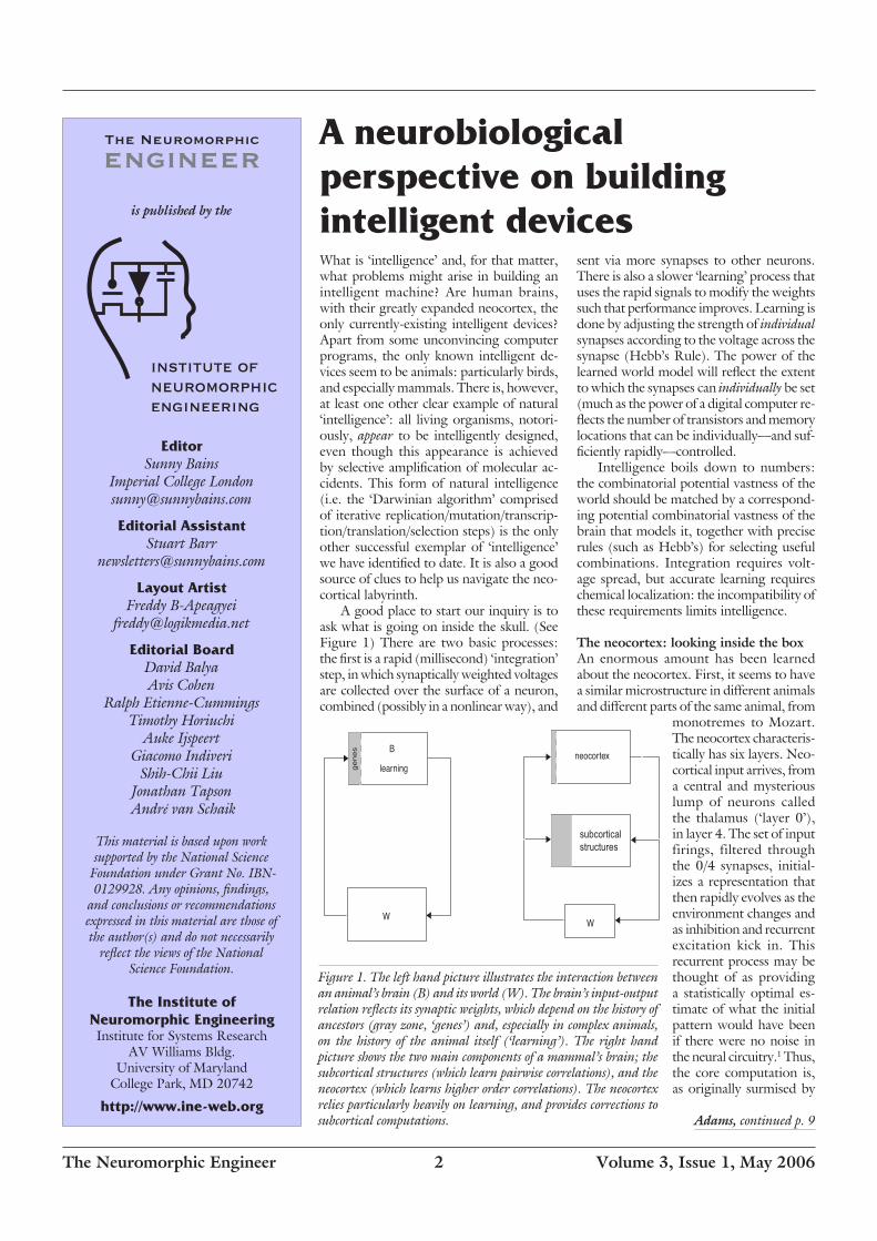
A good place to start our inquiry is to ask what is going on inside the skull. (See Figure 1) There are two basic processes: the first is a rapid (millisecond) ‘integration’ step, in which synaptically weighted voltages are collected over the surface of a neuron, combined (possibly in a nonlinear way), and
sent via more synapses to other neurons. There is also a slower ‘learning’ process that uses the rapid signals to modify the weights such that performance improves. Learning is done by adjusting the strength of individual synapses according to the voltage across the synapse (Hebb’s Rule). The power of the learned world model will reflect the extent to which the synapses can individually be set (much as the power of a digital computer re-flects the number of transistors and memory locations that can be individually—and suf-ficiently rapidly—controlled.
Intelligence boils down to numbers: the combinatorial potential vastness of the world should be matched by a correspond-ing potential combinatorial vastness of the brain that models it, together with precise rules (such as Hebb’s) for selecting useful combinations. Integration requires volt-age spread, but accurate learning requires chemical localization: the incompatibility of these requirements limits intelligence.
Theneocortex:lookinginsidetheboxAn enormous amount has been learned about the neocortex. First, it seems to have a similar microstructure in different animals and different parts of the same animal, from
B
W
learninggene
s
neocortex
W
Figure 1. The left hand picture illustrates the interaction between an animal’s brain (B) and its world (W). The brain’s input-output relation reflects its synaptic weights, which depend on the history of ancestors (gray zone, ‘genes’) and, especially in complex animals, on the history of the animal itself (‘learning’). The right hand picture shows the two main components of a mammal’s brain; the subcortical structures (which learn pairwise correlations), and the neocortex (which learns higher order correlations). The neocortex relies particularly heavily on learning, and provides corrections to subcortical computations. Adams, continued p. 9
subcorticalstructures
monotremes to Mozart. The neocortex characteris-tically has six layers. Neo-cortical input arrives, from a central and mysterious lump of neurons called the thalamus (‘layer 0’), in layer 4. The set of input firings, filtered through the 0/4 synapses, initial-izes a representation that then rapidly evolves as the environment changes and as inhibition and recurrent excitation kick in. This recurrent process may be thought of as providing a statistically optimal es-timate of what the initial pattern would have been if there were no noise in the neural circuitry.1 Thus, the core computation is, as originally surmised by
TheNeuromorphicEngineer 3 Volume3,Issue1,May�006
The notion of a ‘frame’ of video data has become so embedded in computer vision that it is taken for granted. This is natural, given that the only available input devices have always been frame-based—from drum scanners and videcon tubes to CCDs (charge-coupled devices) and CMOS (complimentary metal-oxide semiconductor) imagers. Also, frame-based imagers have undeniable ad-vantages: they use small pixels, are easy to understand, and are compatible with standard output devices. Are frames the way to go for vision problems, or are they just a holdover from video?
Frames carry a heavy penalty: frame-based vision is centered on a stroboscopic series of snapshots taken at a constant rate. The pixels are sampled redundantly, over and over, even if they have nothing novel to say. Bandwidth and dynamic range are limited by the identical sampling rate and integration time. When a human composes a static picture, these may not be terrible disadvantages, but for machine vision in unsupervised environments, the disadvantages of limited dynamic range and sampling rate can be extremely important.
Over the past decade, a handful of devel-opers have created novel vision sensor devices that adopt the neuromorphic architecture of redundancy-reduced address-event output. (We don’t have room here to discuss imaging devices that don’t reduce redundancy.) Some of these devices abandon frames altogether. Starting from Mahowald’s address-event representation (AER) silicon retina,1 these new devices offer the promise of more ef-fective ways of tackling real-world vision problems.
Mahowald’s AER retina was a demon-stration of a concept device that was unusable for any real world task—in fact it was neces-sary to show it something like a flashing LED to see any sensible response. The University of Pennsylvania’s silicon retina2 marked a major advance by incorporating both sustained and transient types of cells with adaptive spatial and temporal filtering, meaning that the space and time constants vary according to the illumination level and spatio-temporal contrast. This functionality is achieved by the use of tightly coupled log-domain current mode circuits. Of all devices built so far, this one comes closest to capturing key adaptive features of biological retinas. However, the price for this functionality is mismatch: the DC firing rates vary by a factor of 1,000, and one-half of the pixels do not spike at all for moderate contrast. In addition, the use of a passive phototransistor current-gain
Freeing vision from frames
mechanism limits the dynamic range to approximately three decades and leads to a relatively small bandwidth.
The Swiss Center for Electronics and Microtechnology (CSEM) was next to weigh in with two devices.3 Both of these—the first based on current mode, and the second on voltage mode with greatly improved performance—relax the notion of a frame by outputting events after a global reset in the order of spatial contrast, each followed by another event that encodes contour orientation. These chips also are the first to successfully implement steerable filters. They are presently in commercial development for jobs such as lane find-ing, and microlenses are being incorporated to increase the photon catch.
The rate of change of the contrast thresh-old is varied dynamical-ly after reset to control the bus occupation, and the device has a very small 2% contrast mis-match and a large six-decade dynamic range. The CSEM pixel also clamps the photodi-ode reverse voltage at a small value, potentially leading to a substantial reduction in dark cur-rent. Its main draw-backs are that it doesn’t reduce temporal redun-dancy (do temporal de-
rivatives, for example), and is thus limited in temporal resolution to the frame rate. Power consumption at 300mW is about 10× the other devices discussed here.
Johns Hopkins Univer-sity entered the competition in an ISSCC 2005 paper4 with their temporal-differ-ence-event imager, which modifies the traditional active-pixel-sensor (APS) CMOS imager to make a pixel that can detect chang-es in illumination. This synchronous device can store the addresses of pix-els that signal change in a
FIFO (first in, first out), making a new type of clocked AER sensor. Its big advantage is that it offers a normal APS mode with relatively small pixels: disadvantages are the limited two decade dynamic range and the fixed illumination-change threshold, mean-ing that the single threshold for change is useful only when the scene illumination is very uniform.
In our own work reported at ISSCC 2006,5 we built a transient AER vision sen-sor that responds purely to relative changes in intensity, loosely modeling the transient
Figure 2. An Edmund density target with contrast steps of 10% was moved in front of the vision sensor. The response of the vision sensor is largely independent of the illumination, which varies by a factor of 135 (42dB). The right side shows photographs taken with a Nikon 995 digital camera.
X Y
Tim
e [m
s]
~25 rev/sec
Events
0
0 50
100
0 50
100
2 4 6 8
10
Stimulus Vision Sensor Response
Figure 1. The disk depicted on the left side of the figure was spun at approximately 1500rpm. The vision sensor produces events at the leading edge and trailing edges of the black dot. The response is a helix of events in space-time. The time-resolution is approximately 1µ
Delbruck, continued p. 4
TheNeuromorphicEngineer � Volume3,Issue1,May�006
Delbruck, continued from p. 3
pathway in the retina. Our pixel combines an active continuous-time logarithmic photosen-sor with a well-matched, self-timed, switched-capacitor amplifier. Each pixel continuously monitors its photocurrent for changes. It responds with an ON or OFF event that represents a fractional increase or decrease in intensity that exceeds a tunable threshold. Events are communicated asynchronously off-chip on a self-timed bus using AER.
This approach makes efficient use of the AER protocol because events are communi-cated immediately, while pixels that sense no changes are silent. We achieved a good tim-ing resolution down to less than 10µs and a latency of 100µs. Because of the local sensing and computation of the relative changes, we achieved a high intrascene dynamic range of
approximately six decades. In Figure 1 the events generated by a rapidly spinning dot paint a kind of sparkling helix in space time. Figure 2 illustrates the wide dynamic range. Our preliminary work shows that this vi-sion sensor can be used efficiently for some problems because the precisely-timed events are useful without binning them into frames. We are currently exploring these possibilities. It remains to be seen to what extent the lack of a sustained system—a DC response, for example—is a serious disadvantage.
TobiDelbruckandPatrickLichtsteinerInstitute of NeuroinformaticsUNI-ETH ZurichZurich, SwitzerlandE-mail: [email protected]
References1. M. Mahowald, AnanalogVLSIsystemforstereo-scopicvision,Kluwer, Boston, 1994.2. K. A. Zaghloul and K. Boahen, Optic nerve signals in a neuromorphic chip I, IEEETrans.onBiomedicalEngineering,51,pp. 657-6, 2004.3. P. F. Ruedi, et al., A 128×128, pixel 120-dB dynamic-range vision-sensor chip for image contrast and orientation extraction, IEEE J. of Solid-StateCircuits, 38, pp. 2325-2333, 2003.4. U. Mallik, et al., Temporal change threshold detection imager, ISSCCDigestofTechnicalPapers,pp. 362-363, San Francisco, 2005.5. P. Lichtsteiner, et al., A 128×128 120dB 30mW Asyn-chronous vision sensor that responds to relative intensity change, Int’lSolidStateCircuitsConf.(ISSCC),pp. 508-509 (27.9), San Francisco, 2006.
controlled by the motor-neuron output.3 Each joint has an antagonistic muscle pair of flexor and extensor, which are activated by the extensor and flexor motor-neuron, respectively (see Figure 1).
RobotwalkingexperimentsChanging the walking speed of a biped robot on the fly without undermining its dynamical stability is a challenge. With the neuromuscular controller, the walking speed of our robot can be changed on the fly by tuning the threshold of the extensor sensor neuron at the hip joints. Figure 3(A) shows the gait when this threshold is changed greatly and abruptly from 110° to 95° at a time t—indicated with a line in Fig-ure 3(B). The walking speed is immediately changed from 57cm/s to 82cm/s. Although there is no specifically-designed controller in charge of the sensing and control of the transient stage of speed-changing, the natural dynamics of the robot itself and the muscle model properties ensure stabil-ity during the change. A video clip of this experiment can be seen online4.
ConclusionUsing real-time experiments, this study has shown that fast dynamic biped walk-ing can be achieved using a neuromuscular reflexive controller without the need for any trajectory control mechanisms. The natural dynamics of the robot and the viscous elastic muscle model have contributed substantially
Tao, continued from p. 1
to the motion generation of the fast walk-ing gaits, thus simplifying the controller structure.
TaoGeng,BerndPorr,*andFlorentinWörgötter†
Department of PsychologyUniversity of StirlingScotland, UKE-mail: [email protected]*Department of Electronics and Electrical EngineeringUniversity of GlasgowScotland, UKE-mail: [email protected]
†Center for Computational NeuroscienceUniversity of GöttingenGöttingen, GermanyE-mail: [email protected]
References1. G. Taga, A model of the neuro-musculo-skeletal systems for human locomotion, BiologicalCybernetics,73, pp. 97-111, 1995.2. T. Geng, B. Porr, and F. Wörgötter, Fast biped walking via a reflexive neuromuscular-like controller, (submitted to) IEEETrans.onSystems,ManandCybernetics,PartB:Cybernetics,2006.3. T. Geng, B. Porr, and F. Wörgötter, Fast biped walking with a sensor-driven neuronal controller and real-time online learning, Int’lJ.ofRoboticsResearch�5 (3), March 2006.4. http://www.cn.stir.ac.uk/~tgeng/smc/speedchange.mpg.
Figure 3. (A) A series of sequential frames of the walking gait. When the neuron parameter is changed at the time of frame 5, the interval between two adjacent frames is 100ms. (B) Real-time data of the angular position of one hip joint (see the text for more information).
TheNeuromorphicEngineer 5 Volume3,Issue1,May�006
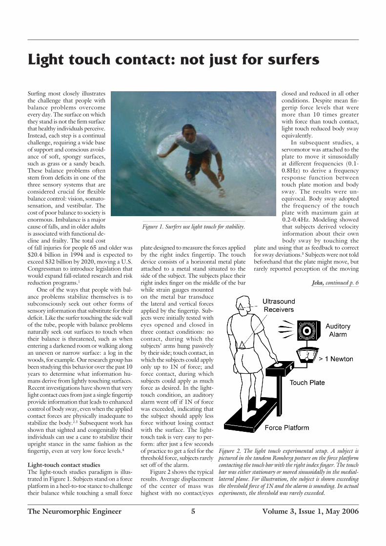
Surfing most closely illustrates the challenge that people with balance problems overcome every day. The surface on which they stand is not the firm surface that healthy individuals perceive. Instead, each step is a continual challenge, requiring a wide base of support and conscious avoid-ance of soft, spongy surfaces, such as grass or a sandy beach. These balance problems often stem from deficits in one of the three sensory systems that are considered crucial for flexible balance control: vision, somato-sensation, and vestibular. The cost of poor balance to society is enormous. Imbalance is a major cause of falls, and in older adults is associated with functional de-cline and frailty. The total cost of fall injuries for people 65 and older was $20.4 billion in 1994 and is expected to exceed $32 billion by 2020, moving a U.S. Congressman to introduce legislation that would expand fall-related research and risk reduction programs.1
One of the ways that people with bal-ance problems stabilize themselves is to subconsciously seek out other forms of sensory information that substitute for their deficit. Like the surfer touching the side wall of the tube, people with balance problems naturally seek out surfaces to touch when their balance is threatened, such as when entering a darkened room or walking along an uneven or narrow surface: a log in the woods, for example. Our research group has been studying this behavior over the past 10 years to determine what information hu-mans derive from lightly touching surfaces. Recent investigations have shown that very light contact cues from just a single fingertip provide information that leads to enhanced control of body sway, even when the applied contact forces are physically inadequate to stabilize the body.2.3 Subsequent work has shown that sighted and congenitally blind individuals can use a cane to stabilize their upright stance in the same fashion as the fingertip, even at very low force levels.4
Light-touchcontactstudiesThe light-touch studies paradigm is illus-trated in Figure 1. Subjects stand on a force platform in a heel-to-toe stance to challenge their balance while touching a small force
Light touch contact: not just for surfers
plate designed to measure the forces applied by the right index fingertip. The touch device consists of a horizontal metal plate attached to a metal stand situated to the side of the subject. The subjects place their right index finger on the middle of the bar while strain gauges mounted on the metal bar transduce the lateral and vertical forces applied by the fingertip. Sub-jects were initially tested with eyes opened and closed in three contact conditions: no contact, during which the subjects’ arms hung passively by their side; touch contact, in which the subjects could apply only up to 1N of force; and force contact, during which subjects could apply as much force as desired. In the light-touch condition, an auditory alarm went off if 1N of force was exceeded, indicating that the subject should apply less force without losing contact with the surface. The light-touch task is very easy to per-form: after just a few seconds of practice to get a feel for the threshold force, subjects rarely set off of the alarm.
Figure 2 shows the typical results. Average displacement of the center of mass was highest with no contact/eyes
closed and reduced in all other conditions. Despite mean fin-gertip force levels that were more than 10 times greater with force than touch contact, light touch reduced body sway equivalently.
In subsequent studies, a servomotor was attached to the plate to move it sinusoidally at different frequencies (0.1-0.8Hz) to derive a frequency response function between touch plate motion and body sway. The results were un-equivocal. Body sway adopted the frequency of the touch plate with maximum gain at 0.2-0.4Hz. Modeling showed that subjects derived velocity information about their own body sway by touching the
plate and using that as feedback to correct for sway deviations.5 Subjects were not told beforehand that the plate might move, but rarely reported perception of the moving
Figure 1. Surfers use light touch for stability.
Figure 2. The light touch experimental setup. A subject is pictured in the tandem Romberg posture on the force platform contacting the touch bar with the right index finger. The touch bar was either stationary or moved sinusoidally in the medial-lateral plane. For illustration, the subject is shown exceeding the threshold force of 1N and the alarm is sounding. In actual experiments, the threshold was rarely exceeded.
Jeka, continued p. 6
TheNeuromorphicEngineer 6 Volume3,Issue1,May�006
plate. They often attributed the increased frequency of body sway driven by touch plate movement to a squishy floor, indicating that cognitive processes influence how the sensor information at the fin-gertip is interpreted.
How do these touch cues serve as a source of sensory information about body orientation? While cutaneous receptors are distributed across the entire body surface, they are particularly dense in the fin-gertip and hand. Analogous to the fovea of the retina, the fingertips are referred to as the somesthetic macula.6 Two-point discrimination studies have shown that the finger-tip can resolve differences as small as 2mm,7 which is approximately the mean level of sway that we observe with light touch contact. Interestingly, two-point discrimi-nation at the bottom of the foot is approximately 8-10mm, which is approximately the mean level of sway observed when subjects stand without fingertip contact and eyes closed.
In summary, a series of studies on postural control with light touch contact of the fingertip have demonstrated that somatosensory cues are a powerful orien-tation reference for improved control of upright stance. The movement of contact forces across the skin surface of remote extremities is providing orientation cues about movement of the body and signaling muscular activation for corrections of body sway. Small applied forces are not capable of physically moving the body, but still provide information about body orientation relative to the surfaces upon which we stand, lean, and touch.
The improvement in balance control observed with a mobility aid such as a cane is often attributed to the cane acting as a third leg, with the concomitant widening of the base of support. The light touch studies argue that in cases of a sensory deficit, improved balance control arises from the precise cues about body sway provided by somatosensory information from the fingertips and hand. The third leg is uniquely different from the real legs. It has the high resolution of the fingertip to detect movement related to body sway, resulting in postural corrections well before
Jeka, continued from p. 5
the boundaries of upright stability.
JohnJekaDepartment of KinesiologyNeuroscience and Cognitive Science and Biomedical Engineering Graduate Pro-gramsUniversity of MarylandCollege Park, MDE-mail: [email protected]://www.hhp.umd.edu/KNES/faculty/jjeka/
References1. H.R. 3695, 20022. J. J. Jeka and J. R. Lackner, Fingertip contact influences human postural control, ExperimentalBrainResearch100, pp. 495-502, 1994. 3. J. J. Jeka and J. R. Lackner, The role of haptic cues from rough and slippery surfaces in human postural control, Ex-perimentalBrainResearch103, pp. 267-276, 1995.4. J. J. Jeka, R. D. Easton, B. L. Bentzen, and J. R. Lackner, Haptic cues for postural control in sighted and blind individuals, Perception&Psychophysics58(3), pp. 409-423, 1996.5. J. J Jeka, K. S. Oie, G. S. Schöner, T. M. H. Dijkstra, and E. Henson, Position and velocity coupling of postural sway to somatosensory drive, J.ofNeurophysiology79,pp. 1661-1674, 1998.6. C. G. Phillips, Movementsofthehand,Liverpool University, Liverpool, 1986.7. C. E. Sherrick and R. W. Cholewiak, Cutaneous sensi-tivity. In K.R. Boff, L. Kaufman and J.P. Thomas (Eds), HandbookofPerceptionandHumanPerformance, pp. 12-24, Wiley, New York, 1986.
Figure 3. Mean center of mass (COM) displacement for each experimental condition. COM displacement was highest in the no contact/eyes closed condition and lowest with any form of fingertip contact.
The SaliencyToolbox version 1.0 has now been released at:
http://www.saliencytoolbox.netThis is a collection of Matlab functions and scripts for computing the saliency map for an image, for determining the extent of a proto-object, and for serially scanning the image with the focus of attention. Being mostly written in Matlab, the code is easily accessible, easy to experiment with, and platform independent. The toolbox requires Matlab Release 13 or 14 and the Image Pro-cessing Toolbox. Most time critical parts of the code are coded in C++ mex files.
Pre-compiled binaries of the mex files are included for Microsoft Windows, Mac OS X, Linux 32 bit Intel/AMD, and Linux 64 bit AMD Opteron. The source code can be compiled on any system with the GNU C compiler gcc. The SaliencyToolbox is licensed under the GNU General Public License.
Parts of the code are reimplemented from the iNVT toolkit at Laurent Itti’s lab at USC. This toolbox complements the iNVT code in that it is more compact (about 5,000 versus 360,000 lines of code) and easier to understand and experiment with, but it only contains the core functionality for attending to salient image regions.
Although time critical procedures are contained in mex files, processing an image with the SaliencyToolbox in Matlab takes longer than with the iNVT code. Whenever processing speed or feature richness is para-mount, the iNVT code should be preferred. For computing the saliency map or attend-ing to salient proto-objects in an image in a transparent and platform independent way, the SaliencyToolbox is a good choice.
This code was developed as part of Dirk Walther’s Ph.D. thesis in the Koch Lab at Caltech, made possible by funding from NSF and NIMH.
DirkWaltherPostdoctoral FellowCentre for Vision ResearchRoom 0009, CSE BuildingYork University4700 Keele StreetToronto, ON M3J 1P3CanadaE-mail: [email protected]@cs.yorku.cahttp://klab.caltech.edu/~walther
Saliency toolbox released
TheNeuromorphicEngineer 7 Volume3,Issue1,May�006
Complex systems developed by neuro-morphic engineers require interfaces to interconnect them, and to connect them to PCs for development, debugging, or other purposes. This concept was the start-ing point for the development of a set of address-event-representation (AER) tools under the European CAVIAR (convolu-tion address-event-representation vision architecture for real-time) project.
Our team is comprised of four part-ners working together in the design of a neuromorphic vision system based entirely on AER principles. CAVIAR connects the biggest AER chain constructed to date.1 The front of the signal chain is composed of a 128×128 ‘retina’ that spikes with temporal and contrast changes,2 four convolution chips that can detect a ball at different distances from the retina,3 and four object chips that filter the convolutional activity.4 This is coupled to a two-chip learning stage comprised of a delay line and a learning element.5 To make such a vision system useable, a set of AER-tools are not only useful, but also necessary, for developing interconnections and debugging.
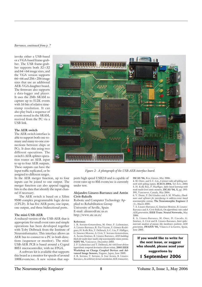
These AER Tools are divided into four different printed circuit boards (PCBs) which, depending on the firmware down-loaded to them, can have eight different functionalities. Our group, the robotics and computer technology (RTC) team, has developed a PCI bus-to-AER interface, that uses the Rome PCI-AER design (developed by Dante) as a starting point. It consists of two universal serial bus (USB)-to-AER interfaces and an AER-to-AER interface. All elements have their own Linux and XP drivers and Matlab interfaces.
ACAVIARPCI-to-AERinterfaceThe PCI bus’s high bandwidth and wide availability of commercial PCI interface silicon makes it an excellent tool for inject-ing and reading events to an AER system, provided a suitable bridging interface to the AER bus can be developed. Our interface differs from the Rome PCI-AER6 in several characteristics: The CAVIAR PCI-AER is not a communications center and does not include a mapper or a splitter/merger. Our PCI-AER interface simply serves as a very fast communication channel (up to 10M events/sec versus. the 1M events/sec capacity of the Rome board) between the AER bus and the PC software.
This system, shown in Figure 1, is
Address-event-representation tools
designed around a Xilinx Spartan II 200 field-programmable gate array (FPGA), with a PCI interface developed in very-high-speed integrated circuit (VHSIC) hardware description language (VHDL) by the RTC group. This makes it cheaper and faster. It has one AER output bus and one AER input bus. Both have their own first-in-first-out (FIFO) buffers that can save the event information and its timestamp for up to 128 events (output) and 256 events (input). The circuit uses a relative timestamp (indicating the distance between consecutive events), but the time controller is able to recover from protocol-induced delays. Therefore, if one event is delayed, the subsequent ones don’t have to be. The timestamp function is configurable for resolutions ranging from 30ns to 480ns per timer tick. The CAVIAR PCI-AER interface supports PCI mastering.
AUSB-to-AERinterfaceWhile a USB-based AER interface delivers less bandwidth than its PCI-based coun-terpart, its smaller size, ease of use, and versatility make it very valuable for many applications. This interface is designed around a Spartan II 200 FPGA and a Cygnal 8051 USB microcontroller: elements that make it fully configurable. The USB inter-face’s maximum throughput is 6Mbits/sec (~187K events/sec), which limits the use of this interface for event based communica-tions between the PC and the board. This allows the interface to receive the control information or frames (bitmaps) from the
PC, whereupon it uses hardware-based frame-to-AER transformations to produce AER events.
The board’s integrated 32-bit wide 2MB SRAM, memory card slot, USB connector and dual AER connectors (as shown in Fig-ure 2), make it a very attractive platform for developing an interesting set of AER tools. The elements of the tool collection can be broken into two categories; PC dependent, and independent. In PC-dependent tools, the USB bus is used both to download FPGA firmware and pass commands and data to and from the interface. When used as a PC-independent tool, the interface’s embedded memory card has the firmware stored and the microcontroller downloads it to the FPGA without the need of a host PC.
This board currently has several avail-able firmware options that provide differ-ent functionalities. The AER generator downloads a frame (bitmap) from a PC and, through a method for synthetic AER generation,7 uses it to create and transmit a sequence of events. One of the generation methods uses a Poisson distribution of events.8 The board’s AER mapper function can be firmware-configured in either a 1-1 or 1-N (with N from 0 to 8) arrangement. Firmware is also available to instantiate a probabilistic version that assigns a prob-ability to each of the possible output events associated to an input event.
The board’s firmware can also be used to
Barranco, continued p. 8
Figure 1: A photograph of the CAVIAR PCI-AER interface board.
TheNeuromorphicEngineer 8 Volume3,Issue1,May�006
Barranco, continued from p. 7
invoke either a USB-based or a VGA-based frame-grab-ber. The USB frame-grab-ber supports both 32×32 and 64×64 image sizes, and the VGA version supports 64×64 and 256×256 image sizes that use an additional AER-VGA daughter board. The firmware also supports a data-logger and player. It uses the 2Mb SRAM to capture up to 512K events with 16 bits of relative time-stamp resolution. It can also play back a sequence of events stored in the SRAM, received from the PC via a USB link.
TheAERswitchThe AER switch interface is able to support both one-to-many and many-to-one con-nections between chips or PCs. It does this using two different operations. The switch’s AER splitter opera-tion routes an AER input to up to four AER outputs. These outputs can have the input traffic replicated, or be assigned to different ranges. In the AER merger function, up to four inputs can be joined to one output. The merger function can also append tagging bits to the data that identify the input chan-nel if necessary.
The AER switch is based on a Xilinx 9500 complex programmable logic device (CPLD). It has five AER ports; one input, one output, and three bidirectional ports.
Themini-USB-AERA reduced version of the USB-AER that is appropriate for small event rates and simple operations has been developed together with Toby Delbruck from the Institute of Neuroinformatics. This interface allows an AER bus to connect to a PC in both direc-tions (sequencer or monitor). The mini-USB-AER PCB is based around a Cygnal 8051 microcontroller, with no FPGA.
A software kit is available that supports this board as a monitor for speeds of around 100Kevents/sec. A new version that sup-
ports high speed USB2.0 and is capable of event rates up to 8M events/sec is currently under test.
AlejandroLinares-BarrancoandAntónCivit-BalcellsRobotic and Computer Technology Ap-plied to Rehabilitation GroupUniversity of Seville, SpainE-mail: [email protected]://www.atc.us.es/
References1. R. Serrano-Gotarredona, M. Oster, P. Lichtsteiner, A. Linares-Barranco, R. Paz-Vicente, F. Gómez-Rodrí-guez, H. Kolle Riis, T. Delbruck, S. C. Liu, P. Häfliger, G. Jimenez-Moreno, A. Civit, T. Serrano-Gotarredona, A. Acosta-Jiménez, B. Linares-Barranco, AER building blocks for multi-layer multi-chip neuromorphic vision systems, NIPS’05,Vancouver, December-2005.2. P. Lichtsteiner and T. Delbruck, 64×64 Event-driven logarithmic temporal derivative silicon retina, �005IEEEWorkshop on Charge Coupled Devices and Ad-vancedImageSensors,Nagano, Japan, June 2005.3. R. Serrano, T. Serrano, A. José Acosta, B. Linares-Barranco, An arbitrary kernel convolution AER-transceiver,
ISCAS’06,Kos, Greece, May 2006.4. M. Oster, and S. C. Liu, A winner-take-all spiking net-work with spiking inputs, ICECS�00�,Tel Aviv, 20045. H. Kolle Riis, P. Haefliger, Spike based learning with weak multi-level static memory, ISCAS’0�,5,pp. 393-395, Vancouver, Canada, May 2004.6. V. Dante, P. Del Giudice and A. M. Whatley, Hard-ware and software for interfacing to address-event based neuromorphic systems, TheNeuromorphicEngineer�(1), March 2005.7. A. Linares-Barranco, G. Jiménez-Moreno, B. Linares-Barranco and A. Civit-Ballcels, On algorithmic rate-coded AER generation, IEEETrans.NeuralNetworks,May 2006.8. A. Linares-Barranco, M. Oster, D. Cascado, G. Jiménez, A. Civit and B. Linares-Barranco, Inter-spike-intervals analysis of poisson like hardware synthetic AER generation, IWANN’05,Vilanova I la Gertru, Spain, June 2005.
Figure 2: A photograph of the USB-AER interface board.
If you would like to write for the next issue, or suggest
who should, please send your suggestions by
1 September 2006
TheNeuromorphicEngineer 9 Volume3,Issue1,May�006
Adams, continued from p. 2
Hubel and Wiesel in their work on the visual cortex,2 a feed-forward input vector-weight matrix-output vector computation that provides an explicit initial representation of the world. This representation is a linear transformation of an already-efficient but less explicit representation furnished by the thalamus.
The thalamic representation is optimal in terms of second or-der (pairwise) statistics only, while the neocortex takes into account re-sidual, higher-order de-pendencies. The thalamic representation is merely a copy of the ‘whitened’ or decorrelated retinal representation that is also sent to more primitive brain areas such as the col-liculus, where immediate actions, based on learned second-order statistics plus inherited knowledge, are initiated. The cortex is an ‘add-on’ device that provides slower, higher-order corrections.3
Hubel and Wiesel originally suggested that the layer 4 ‘simple’ cells are tuned to local orientation because oriented lines and edges are particularly rich in the natural world (and therefore provide a natural ‘code’). Since then, this insight has cor-roborated through more quantitative analysis with tools from information theory, statistics, etc.
Indeed, statistically optimal representa-tion of natural scenes, based on the idea that the mutual information between the scenes and their neural representations should be maximized, leads directly to the concept of local orientation filters, i.e. inde-pendent component analysis (ICA).4 This strategy exploits higher-order redundancies to generate optimal codes. Such a code is ‘generative’ in that it attempts to model the transformation, in the real world, that leads from ‘objects’ and other underlying ‘causes’ to sensory data (patterns of light on the retina etc).
In ICA, the generative model is linear but, in principle, nonlinear processes can also be modeled. This seems to happen in the transformation from simple cells (orientation-tuned and position-sensitive) to complex cells (typically found in layers 2
and 3) that are orientation-tuned but locally position-insensitive. Representations in later layers also incorporate temporal correlations (leading, for example, to direction-tuning). This framework is an appealing, though incomplete, ‘candidate’ for the elusive laurel of ‘canonical microcircuit’. (The canonical microcircuit concept, that there is a core information-processing strategy throughout
the mammalian cortex, is controversial, but without it prospects for hardware emulation seem hopeless, since there would be nothing to emulate).
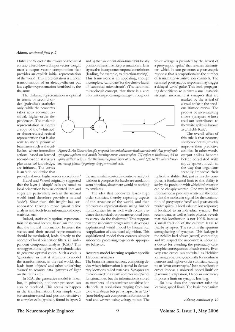
The idea that neocortex learns high order statistics, thereby capturing aspects of the structure of the world, and then reprocesses representations using further nonlinearities fits in well with recent evi-dence that cortical outputs are rerouted back to cortex via the thalamus.5 This suggests that the neocortex progressively develops a sophisticated world model by hierarchical reapplication of a standard algorithm. This sophisticated model then corrects simpler subcortical processing to generate appropri-ate behavior.
Accurate model-learning requires specific HebbiansynapsesThe brain is a nanoelectronic computing de-vice where information is stored in elemen-tary locations called synapses. Synapses are micron-sized units with complex read/write functionalities, but the information is stored as numbers of transmitter-sensitive ion channels, at resolutions ranging from one to several dozen bits per synapse. As in ‘dry’ (non-biological) computers, information is read and written using voltage pulses. The
‘read’ voltage is provided by the arrival of a presynaptic ‘spike,’ that releases transmit-ter, which in turn generates a postsynaptic response that is proportional to the number of transmitter-sensitive ion channels. The summed postsynaptic responses may trigger a delayed ‘write’ pulse. This back-propagat-ing dendritic spike initiates a small synaptic strength increment at synapses that are
marked by the arrival of a ‘read’ spike in the previ-ous 10msec interval. The process of incrementing those synapses whose read-out contributed to the ‘write’ spikes is known as a ‘Hebb Rule’.
The overall effect of this rule is that neurons, and hence brains, steadily improve their predictive abilities. In other words, output spikes become better correlated with input spikes, much in the way that organisms steadily improve their
replicative ability. But, just as in a dry com-puter, a fundamental limit to this ability is set by the precision with which information can be cheaply written. One way in which information is precisely written in the brain is that the molecular signal for the conjunc-tion of presynaptic ‘read’ and postsynaptic ‘write’ spikes (a local calcium ion response) is localized to an individual synapse. But recent data, as well as basic physics, reveals that this localization is not 100% because a small fraction of the calcium leaks to nearby synapses. The result is the spurious strengthening of synapses. This leakage is the Achilles heel of wet (neural) computing, and we suspect the neocortex is, above all, a device for avoiding the potentially cata-strophic consequences of such errors. Even very rare errors can snowball as Hebbian learning progresses, especially for nonlinear neurons and higher-order statistics, leading to an ‘error catastrophe.’ Just as replication errors impose a universal ‘speed limit’ on Darwinian adaptation, Hebbian inaccuracy imposes a limit on synaptic learning.
So how does the neocortex raise the learning speed limit? The basic mechanism
Adams, continued p. 10
Figure 2. An illustration of a proposed ‘canonical neocortical microcircuit’ that proofreads synaptic updates and avoids learning error catastrophes. T/J refers to thalamus, 4/I to spiny stellate cells in the thalamorecipient layer of cortex, and 6/K to the coincidence-detecting plasticity-gating deep pyramidal cells.
J I
TheNeuromorphicEngineer 10 Volume3,Issue1,May�006
LABORATORY NOTESCharge-based CMOS realization of unconventional functionsNeuromorphic systems make use of a set of specific functions that exhibit specific or unconventional behavior. These include winner-take-all (WTA), weighted average, and thresholding, functions. These can be integrated using various design tech-niques, such as analog or digital, standard or subthreshold realizations. In this paper, we present a brief survey of charge-based realizations of several functions. These can be used as building blocks in the synthe-sis of larger-scale CMOS integration of neuromimetic circuits, using as an atomic functional operator the capacitive threshold logic (CTL) circuit presented earlier.1
Modified CTL gateThe basic CTL gate consists of a floating central node, called a row on Figure 1, that
is capacitively-coupled to input signals and connects to a thresholding unit. In its sim-pler form, the thresholding unit is formed by a CMOS inverter circuit, but faster op-eration can be obtained using a differential realization.2 CTL gate operation consists of a prechage phase (Φ1) where all circuit nodes are set to reference voltages, followed by an evaluation phase (Φ2), where all circuit node voltages are influenced by selected input values. Inaccuracies in the absolute values of the integrated capacitances are cancelled by the fact that all operations rely on capacitance ratios, exclusively.
Considering only the analog column as input, the operation realized by this circuits consists of a weighted average of its inputs (Equation 1), followed by thresholding by the CMOS first inverter stage (Equation
2). An obvious modification of the basic gate consists of including bias capacitances, which are used in the same precharge-evalu-ation scheme to modify the relative value of the threshold .3 In a similar way, a perturba-tion capacitance is connected to the central node. It is operated using a third clock phase (Φ3), which is taking place at the end of the evaluation phase in an overlapping way. A perturbation signal may consist of a ramp or a pulse of calibrated amplitude, allowing the detection of the actual row voltage.4
CombinedgatesrealizationThe mixed use of CTL-CMOS logic gates is applied in the synthesis of Multiple-Val-ued Logic (MVL) operators, such as the literal gate, MVL-NAND/NOR, whereas the use of an averaging circuit allowing level recovery allows the synthesis of complex MVL transfer functions, such as the T-gate, NMIN/NMAX functions.5
Cascading the charge-based stages into a configuration consisting of a CTL first
Figure 1. Modified capacitive threshold gate, using threshold biasing and row voltage perturbation inputs; multiple analog columns (n) may be connected.
∆VV V C
Crow
A ref ATOT
i
n
ATOT
i
=−( )
=∑
1 Equation 1
∆VV V C
Crow
A ref ATOT
i
n
ATOT
i
=−( )
=∑
1 Equation 2
Leblebici, continued p. 11
Adams, continued from p. 9
(as in accurate DNA copying) may be Heb-bian ‘proofreading’ (see Figure 2).6
The Hebbian connection from J to I (representing, for example, a thalamocorti-cal connection) can undergo strengthen-ing as a result of coincident firing of the J and I cells, but this strengthening is not 100% precise, and may lead to a learning catastrophe (weights randomize). This can be prevented using a second independent assessment of coincidence using a special ‘K’ neuron, which then ‘gates’ the plasticity of the feed-forward connection. The gat-ing signal is fed to both the input (J) and output (I) cell, and conjunction of pre- and postsynaptic gating signals is required for Hebbian updates to occur. This circuit closely resembles those found in the neocor-
tex but, as of this writing, the proofreading hypothesis is unproven.
In all known examples of intelligence (evolution, brains, and computers) the key step is writing information accurately. Future intelligent neuromorphic devices will also require accurate ‘synapses,’ and, probably, neocortex-like ‘proofreading.’ It’s likely that while we are using super-computers to understand the brain,7 we will need to understand the brain to build hypercomputers.
PaulAdamsandKingsleyCoxDepartment of Neurobiology SUNY Stony Brook, NY E-mail: [email protected]://syndar.org
References1. A. Pouget, P. Dayan and R. S. Zemel, Inference and computation with population codes, Annu.Rev.Neurosci.�6, pp. 381-410, 2003.2. D. Hubel and T. Wiesel, Receptive fields, Binocular interaction and functional architecture in the cat’s visual cortex. J. of Physiol. (London) 160, pp. 106-154, 1962.3. R. W. Guillery, Branching thalamic afferents link action and perception, J.Neurophysiol. 90, pp. 539-548, 2003.4. A. J. Bell and T. J. Sejnowski, The “independent com-ponents” of natural scenes are edge filters, VisionResearch37, pp. 3327-3338, 1997.5. S. M. Sherman and R. W. Guillery, Exploring the Thalamus, Academic Press, San Diego, 2001.6. P. R. Adams and K. J. A. Cox, A new interpretation of thalamocortical circuitry. Phil.Trans.Roy.Soc.B.357, pp.1767-1779, 20027. H. Markram, The blue brain project, NatureReviewsNeuroscience7, pp.153-160, 2006.
TheNeuromorphicEngineer 11 Volume3,Issue1,May�006
stage, followed by a degenerated CTL sec-ond stage, and a level recovery circuit allows the synthesis of unconventional functions as depicted in Figure 2(a) and Figure 2(b).
The hardware integration of the Ham-ming artificial neural network has been pro-posed6 where an analog WTA is integrated. A modified version using programmable capacitance weights has been proposed.7 The CTL gate using bias and perturbation capacitances has also been demonstrated,8 where the perturbation capacitance is used to transfer the circuit results into the time-domain. this allows subsequent use of low-overhead digital circuits, mainly consisting of counters and latches, in order to process k-winner-take-all/k-loser-take-all functions and image processing applications such as pattern alignment.
The microelectronic integration of the proposed circuits requires the implementa-tion of a number of double-poly capacitances on-chip to handle charge-based operations. Several circuits have been integrated in various fabrication technologies including 0.8µm, 0.5µm, and 0.35µm CMOS. Full functionality could be demonstrated using relatively small unit capacitances of typically, 20fF, 40fF, and 50fF. The circuit response time depends on the actual implementation. Worst-case response times of less than 10ns are typically observed, whereas the fastest gates switch in less than 5ns. The charge-based gate should not be considered as a direct replacement of CMOS logic in the synthesis of basic Boolean operators, where CMOS is clearly superior in terms of speed.
Leblebici, continued from p. 10
However, in the synthesis of complex or unconventional functions, charge-based gates are competitive with respect to CMOS in terms of functional processing speed and chip area, due to the inherent analog processing of the CTL gate.
AlexandreSchmidandYusufLeblebiciMicroelectronic Systems LaboratorySwiss Federal Institute of Technology EPFLCH-1015 Lausanne, SwitzerlandE-mail: {alexandre.schmid, yusuf.leblebici}@epfl.ch
Rererences1. H. Ozdemir, A. Kepkep, B. Pamir, Y. Leblebici, U. Cilingiroglu, A capacitive threshold logic gate, IEEEJ.Solid-StateCircuits, 31, pp. 1141-1150, August 1996.2. R. Baumgartner, Capacitive circuit architectures for realization of compact ripple-flash analog-digital converters, DoctoralDissertation, Worcester Polytechnic Institute, Worcester, MA, 2001.3. A. Stokman, S. D. Cotofana, S. Vassiliadis, A versatile threshold logic gate, Proc. �1st Int. SemiconductorConf., pp. 163-166, 1999.4. S. Badel, A. Schmid, Y. Leblebici, A VLSI hamming artificial neural network with k-winner-take-all and k-loser-take-all capability,Intl.JointConf.NeuralNetworksIJCNN, pp. 977-982, 2003.5. A. Schmid, Y. Leblebici, Realization of multiple-valued functions using the capacitive threshold logic gate, IEEProc.-Comput.Digit.Tech., 151 (6), pp. 435-447, November 2004.6. U. Cilingiroglu, A charge based neural hamming classifier, IEEE J. Solid-State Circuits, �8 (1), pp. 59-67, 1993.7. A. Schmid, Y. Leblebici, D. Mlynek, Mixed analog-digital artificial neural network architecture with on-chip learning, IEEProc.-Circuits,DevicesandSystems, 1�6 (6), pp. 345-349, December 1999.
and for discussions of the needs of various users from labs around the world. Par-ticipant feedback was quite positive, and continuing discussion on a blog or website was the most-commonly expressed desire. We feel that our community needs many more workshops of this kind, by various experts on different topics, and that this type of intense, goal-oriented workshop provides both camaraderie and inspiration that generate excitement.
Figure 2. Unconventional transfer functions observed using a cascade of charge-based gates; (a) Synthesis of a non-symmetrical pyramidal transfer function (trace 1 is input and trace 2 is output), and (b) exotic transfer function surface, composed of a large number of steps.
(b)
(a)
Participants:Tara Hamilton, University of Sydney, AustraliaHisham Ahmed Abdalla, University of Maryland, MDSrinjoy Mitra, Institute for Neuroinformatics, ETH Zurich, SwitzerlandMiriam Marwick, Johns Hopkins University, MDBeatriz Olleta, Johns Hopkins University, MDDavid Sander, University of Maryland, MDAlfred Haas, University of Maryland, MDMike Chi, Johns Hopkins University, MDZhengming Fu, Yale University, CTAndreas Andreou, Johns Hopkins University, MDEugenio Culurciello, Yale University, CTViktor Gruev, University of Pennsylvania, PA
TimothyK.HoriuchiandKwabenaBoahen*Department of Electrical and Computer-EngineeringInstitute for Systems Research Neurosciences and Cognitive Sciences ProgramUniversity of MarylandCollege Park, MDE-mail: [email protected]*Department of BioengineeringStanford UniversityStanford, CA E-mail: [email protected]
Horiuchi, continued from p. 12
TheNeuromorphicEngineer 1� Volume3,Issue1,May�006
The INE/UPenn word-serial address-event representation workshopSince the beginning of neuromorphic VLSI (very-large silicon integration), designers have been grappling with the problem of transmitting thousands of neural signals on and off chips. Starting with the pioneering work of Sivilotti and Mahowald, the re-search community has largely stuck with an asynchronous event-driven interface where a silicon neuron’s digital address is transmit-ted when it spikes. As such, log2(N) shared wires replace N dedicated wires. These address-events, as they are called, utilize the speed of metal wires, which is wasted when a wire is dedicated to a single neuron. Sharing bandwidth this way enables larger neural networks to be built. Also, address-events can be rerouted, whereas metal wires cannot. While most of the improvements in
this approach have focused on mechanisms for routing and broadcasting spikes between chips and computers, little has changed in the actual protocol.
Until recently, the existing protocol could not be expanded to handle systems with multiple senders and receivers without adding significant external circuitry because this decade-old technique did not distin-guish one chip from another. The Boahen lab at the University of Pennsylvania created a new protocol that addresses this limita-tion. The word-serial address-event repre-sentation (AER) appends chip addresses to the neuron’s row and column addresses,
all of which are transmitted sequentially, thereby distinguishing events from differ-ent chips. In addition to being expandable, word-serial is efficient: it cuts the number of address lines in half.
While creating a new protocol for com-munication that is expandable is an academic achievement, it only becomes useful if it is adopted by many users. To promote this new approach and facilitate its adoption, we obtained financial support from INE and organized a short, focused workshop to train students and faculty on the word-serial AER concept and on automated tools for its implementation. We also received a gener-ous donation of CAD software (Tanner Tools Pro) from Tanner Research. After so-liciting applications from advanced students
and interested faculty, we selected a group to meet 1-5 December, 2005 at the University of Pennsylvania campus in Philadelphia. INE paid the travel expenses of domestic applicants and the lodging expenses of all non-faculty workshop participants at a hotel on campus. A conference room on campus was filled with rented computer systems loaded with the Tanner Tools Pro package and the Boahen Lab’s chip-design tools. In addition to the organizers, we enlisted the help of two dedicated teaching assistants: Joseph Lin and Paul Merolla, both from the Boahen Lab.
The primary goal of our workshop was
to have participants leave with the finished layout of a chip design that incorporates a core circuit from their particular research area into a word-serial AER transmitter and/or receiver frame. All designs were to be compatible with the L-Edit software suite upon arrival. While this was a bur-den for some participants, it was the only practical way to ensure a completed chip in three days.
One important component of the work-shop was the requirement that every partici-pant arrive having read the tutorial docu-ment and with a completed pixel layout, plus schematics. Joseph Lin was assigned to pester everyone two weeks ahead of time to send in their layout and schematics so that he could check them. We asked everyone to give a 10 minute talk at the beginning of the workshop to present their pixel design and explain what their overall plan was for a chip. On the first day, Joseph Lin gave a short lecture on the ChipGen tool for com-piling AER chips developed in the Boahen Lab. Kwabena Boahen gave two lectures describing the evolution of the particular transceiver implementation that ChipGen was compiling and the types of output the fabricated chip would produce. He also presented a vision for the future of AER and multichip neuromorphic systems.
Projects brought by the participants included: a 2D current-mode cochlea with AER neurons; an ultrasonic cochlea with a 2-D array of AER neurons; a high-resolu-tion avalanche diode array imager; a 2D neuron transceiver chip; a contact imager for detecting the location of cell shadows; a spiking neuron imager with correlated double-sampling; and a 2D change-detec-tion retina that signals using AER spikes.
Because of the workshop’s short length, accomplishing our goals required dedica-tion, as well as prior preparation. While we were proactive in urging that everyone arrive prepared, it was difficult to anticipate the miscommunication and confusion on certain aspects of ChipGen’s operation, a result of insufficient detail in the docu-mentation we provided. We resolved these questions at the workshop, but precious time was lost.
Overall, the workshop was a great opportunity for intense interaction with students interested in utilizing ChipGen,