Linköping Studies in Science and Technology Dissertation No. 1488 Valence Electron Energy Loss Spectroscopy of III-Nitride Semiconductors Justinas Pališaitis Thin Film Physics Division Department of Physics, Chemistry and Biology (IFM) Linköping University, Sweden 2012
Transcript
Linköping Studies in Science and Technology Dissertation No. 1488
Valence Electron Energy Loss Spectroscopy of
III-Nitride Semiconductors
Justinas Pališaitis
Thin Film Physics Division
Department of Physics, Chemistry and Biology (IFM) Linköping University, Sweden
2012
Cover image
The cover image shows a mirror-reflected experimental Valence Electron Energy
Loss Spectrum line scan obtained across an Al1-xInxN (0≤x≤1) multilayer grown on
Al2O3. The spectrum intensity is projected and represented in a temperature scale.
The bulk plasmon peaks have a green color in In-rich AlInN layers, which gradually
shift downwards towards higher energy and turn to yellow (higher intensity) when
This doctorate thesis covers both experimental and theoretical investigations of the
optical responses as determined by the material properties of the group III-nitrides
(AlN, GaN, InN) and their ternary alloys. The goal of this research has been to
explore the usefulness of Valence Electron Energy Loss Spectroscopy (VEELS) for
materials characterization of group III-nitride semiconductors at the nanoscale. The
experiments are based on the evaluation of the bulk plasmon characteristics in the
low energy loss part of the EEL spectrum since it is highly dependent on the
material’s composition and strain. This method offers advantages as being fast,
reliable and sensitive. VEELS characterization results were corroborated with other
experimental methods like X-ray Diffraction (XRD) and Rutherford Backscattering
Spectrometry (RBS) as well as full-potential calculations (Wien2k). Investigated
III-nitride structures were grown using Magnetron Sputtering Epitaxy (MSE) and
Metal Organic Chemical Vapor Deposition (MOCVD) techniques.
Initially, it was demonstrated that EELS in the valence region is a powerful method
for a fast compositional analysis of the Al1-xInxN (0≤x≤1) system. The bulk plasmon
energy follows a linear relation with respect to the lattice parameter and composition
in Al1-xInxN layers. Furthermore, the effect of strain on valence EELS was
investigated. It was experimentally determined that the AlN bulk plasmon peak
experiences a shift of 0.156 eV per 1% volume change at constant composition. The
experimental results were corroborated by full-potential calculations which showed
that the bulk plasmon peak position varies nearly linearly with the unit-cell volume,
at least up to 3% volume change.
Employing the bulk plasmon energy loss, compositional characterization was
applied to confined structures, such as nanorods and quantum wells (QWs).
Compositional profiling of spontaneously formed AlInN nanorods with varying In
concentration was realized in cross-sectional and plan-view geometries. It was
established that the structures exhibit a core-shell structure, where the In
concentration in the core is higher than in the shell. The growth of InGaN/GaN
multiple QWs with respect to composition and interface homogeneities was
investigated. It was found that at certain compositions and thicknesses of QWs,
where phase separation does not occur due to spinodal decomposition, QWs
develop quantum dot like features inside the well as a consequence of Stranski-
Krastanov-type growth mode, and delayed In incorporation into the structure.
ii
The thermal stability and degradation mechanisms of Al1-xInxN (0≤x≤1) films with
different In contents, stacked in a multilayer sample, and different periodicity
Al1-xInxN/AlN multilayer films, was investigated by performing a thermal annealing
in combination with VEELS mapping in-situ. It was concluded that the In content in
the Al1-xInxN layer determines the thermal stability and decomposition path. Finally,
the phase separation by spinodal decomposition of different periodicity AlInN/AlN
layers, with a starting composition inside the miscibility gap, was investigated by
thermal annealing and VEELS mapping in-situ.
iii
Populärvetenskaplig sammanfattning
Halvledarmaterial och halvledarteknik baserad på strukturer i nanostorlek har en
stor påverkan på vårt dagliga liv genom ”smarta” elektroniska apparater. Storleken
på halvledarapparater minskar ständigt på grund av behovet av miniatyrisering,
högre processorhastigheter, nya funktioner och lägre kostnader, vilket kontinuerligt
ställer högre krav på materialet som används i dessa apparater.
En viktig grupp hos halvledarmaterialen är grupp III-nitrider, som har unika
fysikaliska egenskaper och som har skapat ett stort intresse för nutida och framtida
tillämpningar inom optoelektronik och transistorer med höga strömmar och
spänningar.
Dessvärre finns det fortfarande en del utmaningar kvar relaterade till grupp III-
nitrider, såsom avsaknad av naturligt substrat, olika tillväxtvillkor, fasseparation,
termisk stabilitet med mera.
För att kunna överkomma dessa utmaningar behöver kontrollen av och förståelsen
för tillväxt- och diffusionsmekanismer tillsammans med kunskap om
sammansättning och struktur öka genom karakterisering av materialet med hjälp av
nya metoder.
För att åstadkomma detta behövs hög rumslig upplösning vilket kan uppnås genom
att använda ett transmissionselektronmikroskop (TEM), där upplösningen för
nuvarande är betydligt bättre än avståndet mellan två atomer. TEM kombineras ofta
med spektroskopiska metoder för sammansättningsanalys såsom energi-dispersiv
röntgenspektroskopi (EDX) och elektron energi förlust spektroskopi (EELS) , vilket
är en metod där energiförlusten hos elektronerna efter att de spridits genom
materialet studeras.
Den här doktorsavhandlingen täcker både experimentella och teoretiska
undersökningar av de optiska egenskaperna, och därmed även materialegenskaper,
hos grupp III-nitriderna (aluminiumnitrid, galliumnitrid och indiumnitrid) och
deras trefasiga legeringar. Målet med forskningen har varit att undersöka om energi
förlust spektroskopi av valenselektroner (VEELS) kan användas för
materialkarakterisering av grupp III-nitrider i nanoskala. Experimenten baseras på
utvärderingar av egenskaperna hos bulkplasmoner i lågenergiförlustområdet av
EEL-spektrumet, eftersom det är väldigt beroende av materialets sammansättning
och spänningar i materialet. Denna metod har flera fördelar såsom snabbhet,
iv
pålitlighet och känslighet. Resultat från VEELS-karakteriseringen bekräftades genom
andra experimentella metoder såsom XRD och RBS (Rutherford Backscattering
Spectroscopy) samt teoretiska beräkningar med Wein2k. Undersökta III-
nitridstrukturer växtes genom MSE (Magnetron Sputtering Epitaxy) och MOCVD
(Metal Organic Chemical Vapour Deposition).
Inledningsvis visades det att EELS i valensområdet är en kraftfull metod för att
analysera sammansättningen av Al1-xInxN-systemet där 0≤x≤1. Energin hos
bulkplasmonerna är linjärt beroende av gitterparametern och sammansättningen i
osträckta Al1-xInxN-lager. Dessutom undersöktes effekten på sträckningar från VEEL-
spektroskopin. Det visades experimentellt att AlN-bulkplasmontoppen flyttades
0,156 eV per procentuell förändring i bulken vid konstant sammansättning. Det
experimentella resultatet bekräftades av fullpotential-beräkningar, vilka visade att
positionen av bulkplasmontoppen varierar linjärt med storleken på enhetscellen,
åtminstone upp till en volymförändring på 3%.
Genom att använda förlusten i bulkplasmonenergin kunde karakterisering av
sammansättningen genomföras på begränsade strukturer, såsom nanorör,
nanohelixar och kvantbrunnar. Sammansättningsanalys av de spontant skapade
AlInN-nanorören/nanohelixarna med varierande In-koncentration genomfördes i
plansnitts- och tvärsnittsgeometrier. Det fastställdes att strukturen uppvisar en kärn-
skalstruktur, där koncentrationen av In i nanorörens/nanohelixarnas kärna är högre
än i skalet. Tillväxten av multipla InGaN/GaN-kvantbrunnar med avseende på
enhetligheten i sammansättning och gränsytan undersöktes. Det upptäcktes av vid
en viss sammansättning och tjocklek på kvantbrunnarna, där fasseparering på grund
av spinodala sönderfall inte sker, utvecklar kvantbrunnarna kvantprickliknande
särdrag inuti brunnen, som en konsekvens av Stranski-Krastanov liknande tillväxt,
där först ett antal atomlager växer och sedan växer ”öar” på dessa lager, och
försenad integrering av In i strukturen.
Mekanismerna för termisk stabilitet och -nedbrytning för varierande In-
koncentration i Al1-xInxN-filmer (0≤x≤1), staplade som multilager, och Al1-xInxN-
supergitter undersöktes genom termisk härdning i kombination med VEELS-
kartläggning in-situ. Det visades att In-koncentrationen i Al1-xInxN-lagret bestämmer
den termiska stabiliteten och -nedbrytningen. Slutligen undersöktes fasseparering på
grund av förändring i lösbarheten i en III-nitrid, genom termisk härdning och
VEELS-kartläggning in-situ.
v
Preface
The work presented in this doctoral thesis was conducted from fall 2007 to fall 2012
in the Thin Film Physics Division at Department of Physics, Chemistry and Biology
(IFM) at Linköping University (LiU). The goal of my research was to explore the
capabilities of valence electron energy loss spectroscopy for group III-nitride
semiconductors characterization on the nanoscale. This work was supported by the
Swedish Research Council (VR) through a project and Linnaeus grants, the European
Research Council (ERC) as well as the Swedish Foundation for Strategic research
(SSF) through the Nano-N program and CeNano. This thesis is a continuation of my
Licentiate thesis ‘Electron Energy Loss Spectroscopy of III-Nitride Semiconductors’
(Licentiate thesis No. 1487, Linköping Studies in Science and Technology, 2011).
Being part of a graduate school at LiU was educational and enjoyable experience,
which resulted in my thesis. This would not be possible without contribution from
many people who inspired, guided and assisted me during those years. I would like
to express sincere gratitude to all and special thanks go to my supervisor
Per Persson, co-supervisors Lars Hultman & Jens Birch, co-authors & collaborators,
colleagues at Thin Film, Plasma, Nanostructured & Semiconductor Materials groups
and my family & friends.
Justinas Pališaitis
Linköping, November 2012
vi
vii
Included Papers
Paper 1 Standard-free composition measurements of AlxIn1-xN by low-loss
electron energy loss spectroscopy
J. Palisaitis, C.-L. Hsiao, M. Junaid, M. Xie, V. Darakchieva, J.F. Carlin, N. Grandjean, J. Birch, L. Hultman, and P. O.Å. Persson Physica Status Solidi – Rapid Research Letters 5, 50 (2011)
My contribution: I performed TEM/STEM-EELS characterization, took part in XRD and RBS data analysis, and wrote the manuscript.
Paper 2 Effect of strain on low-loss electron energy loss spectra of group III-nitrides J. Palisaitis, C.-L. Hsiao, M. Junaid, J. Birch, L. Hultman, and P. O.Å. Persson Physical Review B 84, 245301 (2011)
My contribution: I performed STEM-EELS characterization, took part in EELS simulation and XRD data analysis, and wrote the manuscript.
Paper 3 Spontaneous formation of AlInN core–shell nanorod arrays by ultrahigh-vacuum magnetron sputter epitaxy C.-L. Hsiao, J. Palisaitis, M. Junaid, R.-S. Chen, P. O.Å. Persson, P. Sandström, P.-O. Holtz, L. Hultman, and J. Birch Applied Physics Express 4, 115002 (2011)
My contribution: I performed STEM-EDX/EELS characterization of AlInN nanorods, contributed in data analysis and in writing the manuscript.
Paper 4 Curved-lattice epitaxial growth of chiral AlInN twisted nanorods for optical applications C.-L. Hsiao, R. Magnusson, J. Palisaitis, P. Sandström, S. Valyukh, P. O.Å. Persson, L. Hultman, K. Järrendahl, and J. Birch Manuscript in final preparation
My contribution: I performed STEM-EDX/EELS characterization of twisted nanorods, contributed in data analysis and in writing the manuscript.
viii
Paper 5 Characterization of InGaN/GaN quantum well growth using monochromated valence electron energy loss spectroscopy J. Palisaitis, A. Lundskog, U. Forsberg, E. Janzen, J. Birch, L. Hultman, and P. O.Å. Persson Manuscript in final preparation
My contribution: I performed STEM-EDX/EELS characterization, analyzed the data and wrote the manuscript.
Paper 6 Thermal stability of Al1-xInxN(0001) throughout the compositional range as investigated during in-situ thermal annealing in a scanning transmission electron microscope J. Palisaitis, C.-L. Hsiao, L. Hultman, J. Birch, and P. O.Å. Persson Submitted to Acta Materialia
My contribution: I performed in-situ annealing experiments, STEM-EELS characterization, analyzed the data and wrote the manuscript.
Paper 7 Spinodal decomposition of Al0.3In0.7N(0001) layers following in-situ thermal annealing as investigated by STEM-VEELS J. Palisaitis, C.-L. Hsiao, L. Hultman, J. Birch, and P. O.Å. Persson Manuscript in final preparation
My contribution: I performed in-situ annealing experiments, STEM-EELS characterization, analyzed the data and wrote the manuscript.
ix
Related Papers, not Included in the Thesis
Paper 8 Room-temperature heteroepitaxy of single-phase Al1-xInxN films with full composition range on isostructural wurtzite substrates C.-L. Hsiao, J. Palisaitis, M. Junaid, P. O.Å. Persson, J. Jensen, Q.-X. Zhao, L. Hultman, L.-C. Chen, K.-H. Chen, and J. Birch Thin Solid Films, in press (2012)
Paper 9 YxAl1-xN thin films A. Zukauskaite, C. Tholander, J. Palisaitis, P. O.Å. Persson, V. Darakchieva, N. B. Sedrine, F. Tasnádi, B. Alling, J. Birch, and L. Hultman Journal of Physics D: Applied Physics, 45 422001 (2012)
Paper 10 InGaN quantum dot formation mechanism on hexagonal GaN/InGaN/GaN pyramids A. Lundskog, J. Palisaitis, C. W. Hsu, M. Eriksson, F. Karlsson, P. O.Å. Persson, U. Forsberg, P.-O. Holtz, and E. Janzen Nanotechnology 23, 305708 (2012)
Paper 11 Microstructure and dielectric properties of piezoelectric magnetron sputtered w-ScxAl1−xN thin films A. Zukauskaite, G. Wingqvist, J. Palisaitis, J. Jensen, P. O.Å. Persson, R. Matloub, P. Muralt, Y. Kim, J. Birch, and L. Hultman Journal of Applied Physics 111, 093527 (2012)
Paper 12 Two-domain formation during the epitaxial growth of GaN (0001) on c-plane Al2O3 (0001) by high power impulse magnetron sputtering M. Junaid, D. Lundin, J. Palisaitis, C.-L. Hsiao, V. Darakchieva, J. Jensen, P. O.Å. Persson, P. Sandström, W.-J. Lai, L.-C. Chen, K.-H. Chen, U. Helmersson, L. Hultman, and J. Birch Journal of Applied Physics 110, 123519 (2011)
Paper 13 Face-Centered Cubic (Al1-xCrx)2O3
A. Khatibi, J. Palisaitis, C. Höglund, A. Eriksson, P .O.Å. Persson, J. Jensen, J. Birch, P. Eklund, and L. Hultman Thin Solid Films 519, 2426 (2010)
x
Paper 14 Electronic-grade GaN(0001)/Al2O3(0001) growth by reactive DC-magnetron sputter epitaxy using a liquid Ga sputtering target M. Junaid, C.-L. Hsiao, J. Palisaitis, J. Jensen, P. O.Å. Persson, L. Hultman, and J. Birch Applied Physics Letters 98, 141915 (2010)
Paper 15 Growth and properties of SiC on-axis homoepitaxial layers J. ul-Hassan, P. Bergman, J. Palisaitis, A. Henry, P.J. McNally, S. Anderson, and E. Janzen Materials Science Forum Vols. 645-648, 83-88 (2010)
Paper 16 Macrodefects in cubic silicon carbide crystals V. Jokubavicius, J. Palisaitis, R. Vasiliauskas, R. Yakimova, and M. Syväjärvi Materials Science Forum Vols. 645-648, 375-378 (2010)
Paper 17 Trimming of aqueous chemically grown ZnO nanorods into ZnO nanotubes and their comparative optical properties M.Q. Israr, J.R. Sadaf, L.L. Yang, O. Nur, M. Willander, J. Palisaitis, and P. O.Å. Persson Applied Physics Letters 95, 073114 (2009)
Paper 18 Two dimensional x-ray diffraction mapping of basal plane orientation on SiC substrates J. Palisaitis, J. P. Bergman, and P. O.Å. Persson Materials Science Forum Vols. 615-617, 275-278 (2009)
Paper 19 AlGaN multiple quantum wells and AlN grown in a hot-wall MOCVD for deep UV applications A. Henry, A. Lundskog, J. Palisaitis, I. Ivanov, A. Kakanakova-Georgieva, U. Forsberg, P. O.Å. Persson, and E. Janzen ECS Transactions, Vol. 25, Iss. 8, (2009)
xi
Paper 20 Stress evolution during growth of GaN (0001)/Al2O3 (0001) by reactive DC magnetron sputter epitaxy M. Junaid, P. Sandström, J. Palisaitis, V. Darakchieva, C.-L. Hsiao, P. O.Å. Persson, L. Hultman, and J. Birch Submitted to Journal of Physics D: Applied Physics
Paper 21 Unexpected behavior of InGaN quantum dot emission energy located at apices of hexagonal GaN pyramids A. Lundskog, C. W. Hsu, J. Palisaitis, F. Karlsson, P. O.Å Persson, L. Hultman, U. Forsberg, P.-O. Holtz, and E. Janzen Submitted to Journal of Applied Physics
Paper 22 Coexistence of 2D/3D growth mode of single GaN nanorods by molecular beam epitaxy Y.-T. Chen, T. Araki, J. Palisaitis, P. O.Å. Persson, L.-C. Chen, K.-H. Chen, P.-O. Holtz, J. Birch, and Y. Nanishi Submitted to Advanced Materials
Paper 23 Liquid-target reactive magnetron sputter epitaxy of high quality GaN(000��) nanorods on Si(111) M. Junaid, Y.-T. Chen, J. Palisaitis, M. Garbrecht, C.-L. Hsiao, P. O.Å. Persson, L. Hultman, and J. Birch Submitted to Nanotechnology
Paper 24 Effect of N2 partial pressure on growth, structure, and optical properties of GaN nanorods grown by liquid-target reactive magnetron sputter epitaxy M. Junaid, Y.-T. Chen, J. Lu, J. Palisaitis, C.-L. Hsiao, P. O.Å. Persson, L. Hultman, and J. Birch Manuscript in final preparation
xii
xiii
Table of Contents
1. INTRODUCTION TO THE FIELD .............................................................................. 1
Materials are vital in the process of human evolution. Therefore, the historical
periods carry the names of the major material that was used in everyday life, e.g.
Stone Age [1].
Which material will take a dominant position and be technologically applied in the
near future, greatly depends on developments and discoveries in material science.
Understanding, predicting, and designing the behavior and properties of a material
are few of the major driving forces for development of new technologies.
Materials analysis is the key component in providing knowledge about the material.
The Ancient Greeks ‘characterized’ materials quality, reliability and found defects in
final products by using nondestructive methods based on human senses like
hearing, touching and smelling [2,3]. The industrial revolution changed the way
people lived, worked and produced goods [4], which increased the demand not only
for novel materials but also for modern material characterization methods. This
marks the start of great fundamental discoveries and developments of the material
characterization methods in physics, which served as the basic principles for the
contemporary material analysis techniques. The development of the electronic
industry in combination with the new characterization methods resulted in
shrinking dimensions of device structures and led to the birth of nanotechnology [5].
This would not be possible without constant development of the characterization
methods which firstly were applied to the bulk type materials and later to the
nanoscale based structures. Nowadays nanotechnology is a very diverse field
covering many disciplines from the material science to medicine. As the size is
reduced to the nanoscale, surface and quantum mechanical effects start to dominate
the material properties exceeding classical physics laws.
The growth of nanostructures is achieved by using contemporary growth methods,
which allow a precise control of the growth parameters and lead to production of the
low-dimensionality structures. Artificially fabricated nanostructures are typically
classified according to the number of dimensions in the nanoscale range.
Nanoparticles and quantum dots (QDs) are zero dimensional nanostructures (0D),
nanorods and nanotubes – 1D; quantum wells (QWs) – 2D. Even more complex
structures, like pyramids, capped with other material, contain QWs on side walls
and wall edges as well as QDs on the top, as shown in Figure 1.
Introduction to the Field
2
Figure 1. Electron microscopy images of nanostructures: (a) Au nanoparticle, (b) AlInN nanorods, (c) InGaN/GaN multiple QWs and (d) GaN pyramid capped with InGaN layer.
Semiconductor materials and technology based on nanoscale structures make a huge
impact on our everyday life by supplying us with ‘smart’ electronic devices. The
trend is continuously moving towards miniaturization of the solid-state devices
driven by the need of compactability, higher processing speed, new functionalities
and lower cost, which puts higher requirements on the materials used [6].
An important part of the semiconductor material group is III-nitride
semiconductors, which own the unique physical properties and attract huge interest
due to their applications for contemporary and future optoelectronic and high-
power devices [7-11]. [7,8,9,10,11]
However, there is a number of remaining challenges related to III-nitrides that were
addressed in a number of scientific studies, for example: lack of native substrate,
different growth conditions, phase separation, etc.
Introduction to the Field
3
In order to conquer these challenges, one needs to control and understand the
growth and diffusion mechanisms along with the compositional and structural
information through material characterization with novel methods.
The material analysis is usually performed on a macro and/or nanoscale. Methods,
employing electrons, ions, and photons, take important part among material analysis
techniques. They can be divided into different categories depending on signal
detected, resolution, etc. A short summary of the most common techniques is given
in Table 1.
Table 1. Analysis techniques employing electron, ion and photon beams.
Incident
beam
Signal
detected
Technique Probes
Electron Electron
Electron
Photon
Electron microscopy
Auger spectroscopy
X-ray emission spectroscopy
Structure & Chemistry
Chemistry
Chemistry
Ion Ion Rutherford backscattering spectrometry Composition
Photon Photon
Electron
X-ray diffraction
X-ray photoelectron spectroscopy
Structure
Chemistry
Rutherford backscattering spectrometry (RBS) and X-ray diffraction (XRD) are
commonly used for the macroscopic compositional and structural investigations.
However, these methods are not adequate to investigate confined structures, like
QWs, QDs, or single precipitates. In order to achieve this, high spatial resolution is
required, which is possible to reach by using the transmission electron microscope
(TEM) where currently the resolution is below the atomic level. TEM is frequently
combined with spectroscopy methods for compositional analysis such as energy
dispersive X-ray spectroscopy (EDX) and electron energy loss spectroscopy (EELS).
In this thesis, valence (V)EELS is employed as the main technique for investigating
group III-nitride materials in combination with other characterization methods. The
valence electron energy loss spectrum region governed by the dielectric function is
rich in information, and provides a tool for sample characterization.
Introduction to the Field
4
Introduction to the Field
5
2. III-Nitride Semiconductors
The core material of today’s semiconductor industry remains Si, however due to
limitations of the physical properties it cannot meet future challenges in emerging
electronic applications, which require device operation at high temperature, power
and frequency. For such applications high thermal conductivity, high breakdown
electric field, tunable band gap as well as thermal, mechanical and chemical stability
are the main prerequisites. A material group exhibiting such physical properties is
III-nitride semiconductors (AlN, GaN and InN), along with their ternary (e.g.,
AlInN) and quaternary alloys (e.g., AlGaInN). Some of the desired properties are
given by a large electro-negativity difference between the group III elements and N,
and establish strong chemical bonds. Group III-nitrides are the key materials for
contemporary electronic devices such as high-brightness blue and white light
The ideal crystal can be built by arranging atoms, molecules or ions in the regular
manner in three dimensions and by keeping long range periodicity. However, real
crystals are decorated with imperfections like impurities and structural defects,
incorporated during the growth process or post-growth treatment. The material
properties are governed by the crystal structure which is defined by periodicity and
symmetries. In general, one can generate 14 basic crystal structures through different
symmetries, called Bravais lattices, in three dimensional space [21].
Group III-nitrides are compound semiconductors formed by alloying group III
elements with N (situated in group V) and commonly found in three crystal
structures: wurtzite, zincblende, and rocksalt [22-24]. [22,23,24]
Two main III-nitride polytype structures: wurtzite which has hexagonal unit cell,
and zincblende which has cubic unit cell, are shown in Figure 2. Under ambient
temperatures and pressures the thermodynamically stable phase is wurtzite (space
group �6�mc) for all bulk III-nitrides and is the most commonly used structure.
III-Nitride Semiconductors
6
Figure 2. Ball-and-stick model of two GaN polytypes: (a) wurtzite (w-GaN), (b) zincblende (z-GaN).
The metastable zincblende-cubic structure (space group �43m) is frequently
reported and can be observed in III-nitride growth on cubic substrates or as a result
of built-in strain in the structure [25,26].
An illustrative example of both crystal structures (wurtzite and zincblende) can be
seen in a GaN nanorod, observed by high resolution TEM (HR-TEM), and is shown
in Figure 3. The small zincblende GaN inclusion is generated after lowering the
growth temperature and results in strain reduction.
Figure 3. HR-TEM image of hexagonal GaN nanorod containing a zincblende GaN inclusion, interfaces are indicated by arrows.
III-Nitride Semiconductors
7
In the wurtzite and zincblende structures atoms are tetrahedraly coordinated (e.g.,
one Ga atom is bound to 4 N atoms), but the stacking sequence and bond angles are
slightly different. The stacking sequence for wurtzite is ABAB… along the c-axis i.e.,
[0001] and for zincblende is ABCABC… along the [111] axis.
Furthermore, the high pressure rocksalt AlN structure was predicted theoretically
and stabilized in epitaxial AlN/TiN superlattices [27]. The rocksalt structures have a
face centered cubic unit cell (space group ��3m).
The most common polytype (wurtzite) is the only structure characterized in this
thesis (Papers 1-7).
Conventionally, planes and directions of crystals are characterized using the Miller
indices. A schematic representation of major crystallographic planes and directions
in the hexagonal and cubic (unit cell) systems are shown in Figure 4.
Figure 4. Major crystallographic directions and planes in (a) hexagonal and (b) cubic unit cells.
Based on crystallographic orientations and directions, the crystal exhibits anisotropic
properties and, as observed in the TEM, different atomic coordination. High
resolution scanning TEM (HR-STEM) images of wurtzite AlN, viewed along the
most common hexagonal unit cell crystallographic projections (zone axes) [1100],
[1120] and [0001] together with schematic images (obtained by the JEMS image
simulation software [28]), are shown in Figure 5.
III-Nitride Semiconductors
8
Figure 5. The HR-STEM images together with schematic illustrations of wurtzite AlN, as viewed along [11�0] (a-b), [1�00] (c-d) and [0001] (e-f) zone axes.
III-Nitride Semiconductors
9
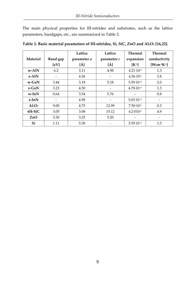
The main physical properties for III-nitrides and substrates, such as the lattice
parameters, bandgaps, etc., are summarized in Table 2.
Table 2. Basic material parameters of III-nitrides, Si, SiC, ZnO and Al2O3 [16,22].
Material
Band gap
[eV]
Lattice
parameter a
[Å]
Lattice
parameter c
[Å]
Thermal
expansion
[K-1]
Thermal
conductivity
[Wcm-1K-1]
w-AlN 6.2 3.11 4.98 4.21·10-6 1.3
z-AlN - 4.36 - 4.56·10-6 2.8
w-GaN 3.44 3.18 5.18 5.59·10 -6 2.0
z-GaN 3.23 4.50 - 4.78·10 -6 1.3
w-InN 0.64 3.54 5.76 - 0.8
z-InN - 4.98 - 5.03·10 -6 -
Al2O3 9.00 4.75 12.99 7.50·10-6 0.3
6H-SiC 3.05 3.08 15.12 4.2·010-6 4.9
ZnO 3.30 3.25 5.20 - -
Si 1.11 5.30 - 3.59·10 -6 1.5
III-Nitride Semiconductors
10
2.2 Polarity and Polarization
Atoms in the III-nitride crystals slightly deviate from their ideal lattice positions.
This induces a lack of the central symmetry perpendicular to the c-axis and hence the
hexagonal crystal structure does not experience the highest symmetry available for
this system. As a result of deviation and strong ionic bonding, III-nitrides become
polar crystals along c-axis with induced macroscopic polarization field [29-31]. [29,30,31]
Polarity leads initially to spontaneous, and if strained, to strong piezoelectric
polarization effects. The polarization field direction and surface properties are
influenced by the polarity of the crystal – the bond direction along the c-axis. When
the direction along the c-axis is started from Ga to N, the surface polarity is defined
as Ga-polar, and vice versa – N-polar (see Figure 6).
Figure 6. Two different polarities of GaN shown together with bond orientation (the crystal viewed along [11�0] zone axis).
In the hexagonal system there also are semi-polar r-plane and nonpolar a-plane and
m-plane (see Figure 4), which are of the significant importance as they do not
experience polarization field [32,33].
The polarity of the grown structure depends on the employed growth technique and
conditions as well as used substrate/buffer layer and can be associated with bonding
configurations at the interface [34]. There is a numbers of ways to determine it, such
as etching, converged beam electron diffraction (CBED), EELS [35,36].
III-Nitride Semiconductors
11
2.3 Bandgap Engineering of Ternary Alloys
Group III-nitrides are attractive materials for optoelectronic applications due to their
band structure which exhibits a direct band gap spanning from ultraviolet (wide) to
infrared (narrow), or from 6.2 eV for AlN to 0.64 eV for InN at room temperatue,
shown in Figure 7.
Figure 7. Energy band gap of III-nitrides and their ternary alloys as a function of the lattice parameter a.
By alloying InN with AlN and GaN the bandgap can be varied from IR to UV in
ternary as well as quaternary systems. The bandgap, as a function of alloying
composition, follows a linear relationship – the Vegards’s law with a correction
factor (called the bowing parameter), which should be taken into account and treats
deviations from the linear dependence among binary alloys [7,37,38].
In general, the bandgap of AlxIn1-xN can be calculated using the following equation:
where �� is the bandgap, x is the Al fraction, and b is the bowing parameter.
The values for the bowing parameter are debated in literature [39], as they differ in
the different compositional regimes. The presence of strain has a profound effect on
the bandgap by reducing it [40].
Al0.83In0.17N is particularly attractive since it can be grown lattice-matched to GaN,
which allows realization of stress free heterostructures with tunable bandgap and
high crystal quality [41].
III-Nitride Semiconductors
12
2.4 Phase Stability
Alloying two binary wurtzite nitrides (e.g., InN and AlN) results in a ternary
compound (AlxIn1-xN). Material properties, such as bandgap, can be varied with
changing the alloy composition (section 2.3), but this comes at the cost of
compositional homogeneity, crystal quality, phase and thermal stability. Theoretical
calculations show that III-nitrides are prone to phase separation [42], since binary
constituents (e.g. InN and AlN) experience large lattice, thermal and chemical
mismatches resulting in large miscibility gap as well as distant growth conditions.
Synthesis of homogeneous solid solutions though entire compositional range is
therefore a challenge. The phase diagram for AlxIn1-xN alloy is shown in Figure 8.
Phase, presented in spinodal region is unstable, and resultant phase separation is
referred to as spinodal decomposition, where binodal phase is metastable.
Figure 8. Phase diagram of AlxIn1-xN alloys [42].
Typically, phase separation occurs when system is quenched below certain critical
temperature and experiences transformation from initially homogeneous solution to
formation of diffusion driven compositional fluctuations. Another approach to
induce phase separation is to synthesize films inside miscibility gap, utilizing, e.g.,
low temperature growth methods (section 3.1), and initiating phase separation by
annealing. Phase separation evolution can be affected by a number of factors such as:
strain [43-45],[43,44,45]composition [42] and additional confinements present in the system
[46]. In the multilayer structure interface layers are the limiting factor for the vertical
elemental diffusion and the surface directed spinodal decomposition might play the
most important role [47,48].
III-Nitride Semiconductors
13
3. III-Nitride Growth
In order to grow a film one applies a flux of atoms from vapor or liquid phase onto a
substrate surface. Thermodynamic and kinematic constrains define the adatom
behavior on the substrate surface and processes like adsorption, desorption, and
diffusion. In any case, the adsorbed atoms strive to minimize their energy by
occupying energetically preferred sites on the substrate surface. The evolution of the
growth is a consequence of minimization of the total energy. Accordingly, the
nucleation and growth process defines the growth mode of the crystal [49].
When a layer of one material is epitaxially grown on a substrate or buffer layer, this
is called hetero-epitaxy. For hetero-epitaxy, the growth mode is primarily influenced
by the lattice parameter differences between the film and the substrate. During
initial stages of growth the first few mono-layers of the epilayer are under tensile or
compressive strain (discussed in 4) in order to adapt to the substrate lattice
parameter. As a result of build-in strain in the film, the film should undergo
transformation to reduce this energy, resulting in different growth modes.
Experimentally, the distinction between the three fundamental hetero-epitaxial
growth modes is well established: Frank-van der Merwe (FM) layer-by-layer growth
(2D), Volmer-Weber (VW) island growth (3D) and Stranki-Krastanov (SK) mixed
growth of layer-by-layer followed by islands formation (Figure 9).
Figure 9. Schematics of three hetero-epitaxial growth modes: Frank-van der Merwe (FM), Volmer-Weber (VW), and Stranski-Krastanow (SK).
Hetero-epitaxial growth modes provide basic understanding, but cannot account for
all factors influencing the growth of novel films. Different strategies can be utilized
to achieve desired structures, e.g., step-flow growth, anisotropic atom fluxes,
catalytic growth.
III-Nitride Growth
14
As discussed in section 2.4, for group III-nitrides it is challenging to achieve a high
crystal quality and homogenous solution through the full compositional range, due
to distant material properties and growth conditions. E.g., InN must be grown at a
lower temperature compared to AlN due to a lower dissociation temperature [50,51].
There are a number of different methods to grow III-nitrides; in this thesis the
investigated III-nitride structures were grown using magnetron sputtering epitaxy
(MSE) and metal organic chemical vapor deposition (MOCVD) techniques.
3.1 Magnetron Sputtering Epitaxy (MSE)
Most of the III-nitride films investigated in this thesis were grown using MSE, which
is a growth method based on the sputtering process [52-55].[52,53,54,55]To initiate the
sputtering process, an inert gas, most often Ar, is introduced into a vacuum
chamber. The basic MSE working principle is shown in Figure 10.
Figure 10. MSE system scheme and fundamental working principle: I - generated plasma, II - sputtering of the target atoms, III - deposition on the substrate.
After igniting the plasma in the vacuum chamber, high (kinetic) energy ions (I) are
accelerated towards one or more targets (II), which are kept at negative potential. In
the sputtering process secondary electrons are generated at the target surface which
helps to sustain ionization of Ar gas. Ions and neutrals are sputtered from the target
towards the substrate surface (III) where a film is grown. Nitrogen (N2) gas is also
introduced into the chamber together with Ar. Nitrogen also acts as a sputtering gas
but reacts with sputtered atoms to form a compound. Compositional variations in
the growing film are achieved by varying the power of the magnetrons. The main
characteristic of the MSE process is that the energy of adatoms is determined by
substrate temperature and kinetic energy of adorbed atom can be varied by applying
III-Nitride Growth
15
a bias to the substrate. Due to the added kinetic energy, growth occurs at non-
thermaldynamic equilibrium conditions.
Al1-xInxN (0≤x≤1) layers and nanostructures studied in Papers 1-4 and 6-7 were
grown in an ultra-high-vacuum (UHV) MSE system (Ragnarök) at LiU. The chamber
has a base pressure of < 4x10⁻⁷ Pa. As material sources, high purity 75 mm-diameter
Aluminum (99.999%) and 50 mm-diameter Indium (99.999%) targets were used.
Typically, Al1-xInxN (0<x≤1) growth was performed under pure nitrogen
environment at ambient temperature and AlN at 1000 oC.
3.2 Metal Organic Chemical Vapor Deposition (MOCVD)
MOCVD is the most commonly used growth technique for depositing III-nitrides
[56,57]. This method is based on a thermally induced reaction of gas-phase precursor
molecules on a heated substrate surface [58,59].
In the case of III-nitride growth, the precursors are supplied as metal-organic
(TMIn), and ammonia (NH3) were used as precursors for Al, Ga, In and N,
respectively, with N as carrier gas [60].
The basic principle of MOCVD together with schematics of the reactor scheme is
illustrated in Figure 11.
Figure 11. MOCVD reactor basic scheme and fundamental working principle: I -precursor, II - dissociation, III - deposition and IV - removal of residual gases.
A mix of precursor gas carrying the desired elements flows through the system in
one direction (I). After entering the high temperature reaction zone, molecules are
dissociated by heat (II) and initiates condensation of the species on the substrate
surface (III). The heat is supplied using radio frequency (RF) coils around the
III-Nitride Growth
16
chamber. Compositional variations in the film are achieved by varying the gas flow
ratio (composition of gas). The remaining reaction products are removed from the
reactor (IV). High purity and high structural quality III-nitride semiconductors with
growth rate of ~2 μm/h can be produced using MOCVD. The growth temperature is
close to thermodynamic equilibrium, as the energy of adatoms depends on
temperature only.
Two III-nitride heterostructure samples containing InGaN/GaN QWs were
investigated in this thesis (Paper 5). The samples were grown in a low pressure hot-
wall MOCVD reactor at LiU. The indium content in the grown QWs was changed
using different TMIn flow rates, in the range from 25 ml/min to 75 ml/min. The
thickness of the QWs was controlled by adjusting the growth time. Typical growth
temperature for QWs was ~800 oC [61,62].
3.3 Template for Growing III-Nitrides
The growth of epitaxial III-nitride semiconductor structures is commonly performed
on foreign substrates (hetero-epitaxy) since native substrates (homo-epitaxy) are
expensive and rarely available [63]. This generally results in a degradation of the
crystal quality of the grown film due to the different crystal structure, lattice
mismatch and thermal expansion coefficients (see Table 2). Crystal structure, price,
physical properties, etc., influence the choice of substrate. By using various growth
strategies high quality epitaxial layers can still be fabricated [64,65]. For instance,
thick buffer layers (of GaN or AlN) can be used to minimize stress and defect
densities in the final structure. Most commonly used substrates are Si, sapphire
(Al2O3) and SiC.
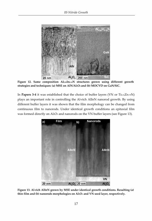
Examples of Al0.84In0.16N structures grown using different growth strategies and
techniques (MSE and MOVCD) are shown in Figure 12. The full compositional range
Al1-xInxN layers investigated in Paper 1 were grown on Al2O3 substrate with a 50 nm
thick high temperature AlN layer (Figure 12a). Another set of Al-rich Al1-xInxN layers
were grown by MOCVD on SiC substrates with GaN buffer layers (Figure 12b). In
both cases buffer layers (AlN and GaN) were used to reduce strain and density of
threading dislocations.
It was demonstrated in Paper 2 that the choice of template and growth temperature
affects the lattice parameter of AlN. The investigated AlN layers were found to be in
relaxed (thick AlN layer grown on Al2O3 at 1000 oC) and oppositely strained states
(thin AlN layer grown on Al2O3 and ZnO at ambient temperature).
III-Nitride Growth
17
Figure 12. Same composition Al0.84In0.16N structures grown using different growth strategies and techniques: (a) MSE on AlN/Al2O3 and (b) MOCVD on GaN/SiC.
In Papers 3-4 it was established that the choice of buffer layers (VN or Ti0.21Zr0.79N)
plays an important role in controlling the Al-rich AlInN nanorod growth. By using
different buffer layers it was shown that the film morphology can be changed from
continuous film to nanorods. Under identical growth conditions an epitaxial film
was formed directly on Al2O3 and nanorods on the VN buffer layers (see Figure 13).
Figure 13. Al-rich AlInN grown by MSE under identical growth conditions. Resulting (a) thin film and (b) nanorods morphologies on Al2O3 and VN seed layer, respectively.
III-Nitride Growth
18
III-Nitride Growth
19
4. Stress and Strain in Thin Films
Epitaxially grown hetero-structures experience an adaptive challenge as two lattices
with different physical properties are forced together. Strain is inevitable in modern
electronic devices, which are increasingly integrating structures with dimensions on
the nanoscale, such as optical devices based on quantum wells [17].
As the structures are geometrically scaled down, the impact of strain has a
significant effect on III-nitride characteristics, such as modulation of the band
structure and electronic transport properties, reduced crystal symmetry, defect
formation, polarization effects, composition pulling effect [66-69]. [66,67,68,69]On the other
hand, strain can be exploited for increasing performance, e.g., in SiGe layer devices
[70,71].
Stress and strain are linked to each other by the elastic constant of the material
according to Hook’s law: if material is stressed – forced it will become strained –
displaced. Strain causes the structure atoms to deviate from their natural equilibrium
positions [72]. The stress is defined as internal force (per unit area) trying to bring
atoms to the equilibrium positions produced by balancing external force acting and
distorting the structure:
� � �, (2)
where F is external force and A – area.
Under applied strain two major scenarios are possible. 1) exceeded critical level of
the strain results in nucleation of defects, such as dislocations, phase transformation,
cracking or delamination – plastic response; 2) moderate amount of the strain can
accommodate by slightly distorting the lattice – elastic response.
In the case of the hexagonal crystal structure (thin film) which is coherently strained
on a relaxed structure (substrate), the in-plane and out-of-plane strains can be
expressed as:
"## � "$$ � %&%'%' , (3)
"(( � )&)')' , (4)
where a0 and c0 are relaxed lattice parameters, a and c - strained lattice parameters.
Stress and Strain in Thin Films
20
If a hexagonal crystal experiences biaxial tensile in-plane stress, it becomes tensely
strained in-plain and compressively out-of-plane due to the Poisson effect as shown
in Figure 14.
Figure 14. As a result of strain, the hexagonal unit cell lattice parameters (a and c) deviate from equilibrium (a0 and c0).
The stress and strain are second rank tensors. As the material behavior is anisotropic
and inhomogeneous, and the properties will be different in different crystallographic
directions. The applied force is a vector and it needs nine components in the matrix
notation for the complete description:
�*+ � ,�## �#$ �#(�#$ �$$ �$(�#( �$( �((-, (5)
.*+ � ,.## .#$ .#(.#$ .$$ .$(.#( .$( .((-. (6)
According to the linear elasticity theory, the relation between induced strain in the
crystal and stress can be expressed as:
�*+ � /*+0�"*+ , (7)
"*+ � 1*+0��*+, (8)
where C and S are stiffness and compliance constants, respectively.
Stress and Strain in Thin Films
21
For a hexagonal crystal the relation between stress and strain finally can be
expressed as:
2334�##�$$�((�$(�#(�#$5
667 �233334
)(2/100000
00000
00000
000
000
000
1211
44
44
331313
131112
131211
CC
C
C
CCC
CCC
CCC
− 566667
2334"##"$$"((2"$(2"#(2"#$5
667
, (9)
where C11, C12, C13, C33, and C44 are elastic stiffness constants.
The origin of strain present in the structure can be lattice mismatch in
heterostructures, different growth conditions, intrinsic stress, and applied external
stress, etc. The film can be found in different strained states (relaxed, partly-relaxed
or strained) resulting in increasing or decreasing unit cell volume. Schematic
examples of differently strained layers are shown in Figure 15.
Figure 15. Schematics showing (a) bulk lattice (substrate and film separated), (b) compressively strained thin film on the rigid substrate and (c) partly relaxed film on the rigid substrate.
Group III-nitrides are typically grown on thermal expansion coefficients mismatched
buffer layers and substrates (see Table 2); the grown structure typically encounters
strain. Three differently strained AlN layers were investigated in Paper 2, the AlN
layers were found to be in relaxed and strained states due to different substrates,
growth temperatures as well as layer thicknesses. AlN grown on different substrates
experiences a lattice mismatch, which for AlN on ZnO and Al2O3 is −4.3% and
+13.3%, respectively.
Stress and Strain in Thin Films
22
Stress and Strain in Thin Films
23
5. III-Nitride Characterization Methods
5.1 Transmission Electron Microscopy (TEM)
The properties of a material are governed by its structure and composition, where
both have to be investigated with high accuracy in order to be fully understood. The
optical microscope has been serving as the major material observation tool for a long
time, but its resolution is limited. In fact, Ernst Abbe showed that optical
microscopes have the diffraction limited resolution, which is proportional to the
ratio between radiation wavelength and aperture size [73]. Later his theory was
refined by Rayleigh for the quantitative measure of the minimum resolvable details
and is known as the Rayleigh criterion [74]. The resolution (d) of an optical system is
conventionally defined as:
8 � 0.61 ;�� , (10)
where λ – wavelength, NA – aperture size.
Due to wavelength of the light, optical microscope resolution can only reach down
to ~200 nm. For overcoming this limit other type of radiation should be used.
The existence of the electron was confirmed by Thomson’s experiments and Louis de
Broglie showed the dualism principle between particles and waves, meaning that
particles traveling at high speed have wave characteristics. Based on the imaging
principle of the optical microscope and employing electrons as the radiation source,
the world’s first TEM was built by Ruska and Knoll in 1932 [75-77].[75,76,77]The wavelength
of the electrons depends on their energy. Taking into account relativistic effects, the
electrons accelerated by 300 kV have wavelength of 1.9 pm. Such short electron
wavelength makes atomic resolution feasible in TEM. The resolution of high-end
TEM microscopes can reach down to 50 pm and even beyond. TEM imaging
techniques are extensively used in academia and industry, where characterization on
the atomic level can provide not just imaging, but also spectroscopic information.
Moreover, the TEM offers a wide range of supplementary information
(crystallographic information about defects, strain, interfaces and boundaries, etc.),
which is available as a result of different operation modes and imaging techniques,
such as bright-field (BF), dark-field (DF) (section 5.2.2), selective area electron
diffraction (SAED) (section 5.2.4) and HR-TEM (section 5.2.5). If an electron probe is
formed by focusing electrons into a fine spot which is scanned across the sample, the
instrument is operated in scanning TEM (STEM) mode (section 5.2.6). It enables
III-Nitride Characterization Methods
24
imaging and analysis on the nanometer scale, including precise EELS and EDX
(sections 5.3-5.4).
The typical limitations of TEM include: small sampling volume, electron beam
damage to the material, and interpretation of images and spectra. Moreover, sample
preparation – which is a demanding and destructive process (section 5.6),
Two microscopes were used for studies in this thesis: FEI Tecnai F20 (200 kV) named
‘Galadriel’ and FEI double-corrected Titan3 (300 kV) – ‘Arwen’.
5.1.1 The Principle of TEM
The basic working principle of TEM is similar to that of an optical microscope. Since
the TEM employs electrons, the microscope must operate at high vacuum
conditions. A basic TEM and STEM scheme is shown in Figure 16. The electrons are
emitted from the electron gun, where the most common types include tungsten (W) -
filament, LaB6, field emission gun (FEG), cold-FEG, high-brightness FEG, where each
differs in brightness, spatial coherence and primary beam energy [78-82]. [78,79,80,81,82]After the
electrons are extracted from the tip of the gun, they are accelerated by a significant
potential difference. Typically, the acceleration voltage can be widely varied from
60 kV to 300 kV. Lower voltage is preferential for studying electron beam sensitive
materials like graphite, higher is used for higher resolution, higher brightness.
After leaving the gun, the electrons are focused by a set of electromagnetic lenses.
The first set of lenses the electron beam encounter is the condenser lens system,
which is used to control the illumination of the sample (intensity and intensity
spread). A number of apertures are used to control the coherency, convergence
angle, current, and centering of the beam.
In the conventional TEM, the beam impinges on the top sample surface as a nearly
planar wave and in STEM as converged electron probe. As the electrons interact
with the sample, they are either transmitted or scattered. Different scattering
mechanisms are used for different imaging techniques (section 5.2). As the electrons
emerge from the bottom sample surface they are again focused by the objective lens
to form an image in TEM and diffraction pattern in STEM. This image is transmitted
by the projection system, consisting of intermediate and projection lenses, onto a
fluorescent viewing screen or a CCD camera.
III-Nitride Characterization Methods
25
Figure 16. Basic outline of the TEM and STEM.
5.1.2 Resolution Limit and Aberration Correctors
Although the wavelength of electrons is on pm range, until recently the resolution of
the microscope was ~1 Å due to technological limitations. The resolution in a TEM is
not diffraction limited as in the case of optical microscopes, but determined rather by
non-ideal imaging characteristics (aberrations) of the lenses, instrumentation
As the coherent electron beam passes through the sample, it experiences coherent
elastic scattering. The scattering occurs as a result of an interaction of the beam with
the periodicity of a crystal structure and is defined to a first approximation by
Bragg’s law (section 5.8). Coherent and elastically scattered electrons from the same
set of atomic planes (at the same Bragg’s angle) are brought to one diffraction spot in
the diffraction plane (back focal plane of the objective lens). In this way a diffraction
pattern is formed, where the central spot consists of the transmitted beam and other
spots originate from the diffracted beams (Figure 19).
Figure 19. The scattered incident beam is focused by the objective lens to form a diffraction pattern in the diffraction plane and the image in the image plane.
III-Nitride Characterization Methods
30
It is possible to generate different images by selecting a specific spot or set of spots in
the diffraction plane (transmitted or diffracted electrons). The selection is made by
the objective aperture, which is inserted in the diffraction plane. Depending on
which electrons are allowed to pass through the objective aperture, the image can be
bright field (BF), which contains the transmitted beam (Figure 20a) or dark field
(DF), which does not (Figure 20b). The objective aperture is primarily used to
increase the contrast of the image and to investigate features, where the contrast
depends on the scattering vector of selected electrons, and can be used, e.g., to reveal
dislocations of different character, local variations in strain, bending and thickness
changes in the sample.
Figure 20. Schematics of different image formation mechanisms in TEM: a) bright field and b) dark field.
III-Nitride Characterization Methods
31
5.2.3 Diffraction in TEM
The diffraction pattern is formed at the same time as the image, and can be viewed
on the screen if the projection system is set to transfer diffraction pattern to the
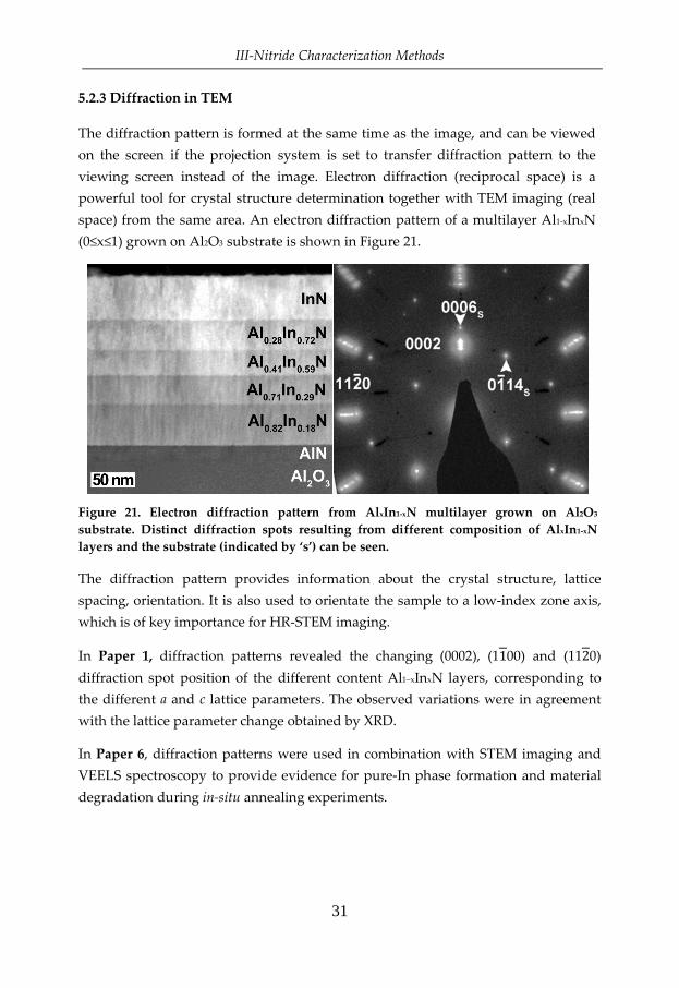
viewing screen instead of the image. Electron diffraction (reciprocal space) is a
powerful tool for crystal structure determination together with TEM imaging (real
space) from the same area. An electron diffraction pattern of a multilayer Al1-xInxN
(0≤x≤1) grown on Al2O3 substrate is shown in Figure 21.
Figure 21. Electron diffraction pattern from AlxIn1-xN multilayer grown on Al2O3 substrate. Distinct diffraction spots resulting from different composition of AlxIn1-xN layers and the substrate (indicated by ‘s’) can be seen.
The diffraction pattern provides information about the crystal structure, lattice
spacing, orientation. It is also used to orientate the sample to a low-index zone axis,
which is of key importance for HR-STEM imaging.
In Paper 1, diffraction patterns revealed the changing (0002), (1100) and (1120)
diffraction spot position of the different content Al1–xInxN layers, corresponding to
the different a and c lattice parameters. The observed variations were in agreement
with the lattice parameter change obtained by XRD.
In Paper 6, diffraction patterns were used in combination with STEM imaging and
VEELS spectroscopy to provide evidence for pure-In phase formation and material
degradation during in-situ annealing experiments.
III-Nitride Characterization Methods
32
5.2.4 Selective Area Electron Diffraction (SAED)
SAED is used to obtain diffraction patterns from specific sample areas. The area
selection is made by inserting the SAED aperture in an image plane. This is an
important tool to obtain information from a desired area, for example, from single
grains in polycrystalline sample, precipitate, orientation relationships between
different phases. As an example, a SAED pattern obtained from the Al2O3 substrate
and the first two layers, AlN and Al0.82In0.18N, is shown in Figure 22.
Figure 22. STEM image and SAED pattern taken from Al2O3 and the first two layers of AlN and Al0.82In0.18N (aperture position indicated by circle).
In Paper 4, SAED patterns were recorded from the twisted nanorod structure. A
hexagonal diffraction pattern with semi-arcs implies a [0001] zone axis and slight in-
plane misorientation between these twisted nanorods. By extracting intensity line
profile across one of the semi-arcs center, an asymmetric peak with a long tail
towards the specular center was obtained, revealing a gradient of lattice constant in
the twisted nanorods.
III-Nitride Characterization Methods
33
5.2.5 Phase Contrast (HR-TEM)
High resolution imaging is used for ‘direct’ observation of the sample lattice (atomic
column projections) in TEM mode. Phase contrast is dominant at high
magnifications (>500 kx) where the electron waves experiences a phase shift as it
interacts with the projected atomic potentials of the sample atoms. After interacting
with the sample, transmitted and scattered electron waves overlap and interfere in
the image plane, forming lattice fringes, an example is shown in Figure 23. More
than one beam is required for phase contrast imaging.
Figure 23. HR-TEM image of GaN. Line intensity profile is indicated (S-F), showing separation between the atomic columns of ~2.8 Å.
In addition to the phase shift due to the crystal potential, the wave is phase shifted
by the microscope phase factor which is a complex function. It depends on many
different parameters, such as: electron wavelength (λ), defocus (C1), different order
lens aberrations (astigmatism (A), spherical aberrations (Cs), coma (B), etc.),
scattering and illumination angles, degree of electron source coherence and is
conventionally defined by the so called phase contrast transfer function (CTF) [85],
which can be expressed as: /<� � =�> ?� @A*; B�CC��D , (11)
where B is aberration function of the microscope and ω is a complex scattering angle (C� is its complex conjugate).
III-Nitride Characterization Methods
34
The HR-TEM contrast dependence on different lattice spacing’s at certain
microscope settings is given by the CTF. In conventional (non-aberration corrected)
TEM aberration function mainly depends on spherical aberration and defocus:
B�CC�� � E@/ECC� � EF/G�CC��@ (12)
For a microscope equipped with a Cs image corrector, Cs can be set to zero. Thus Cs is
no longer a limiting factor, which should result in zero-contrast imaging. However,
this is not the case, since the aberration function is still not cancelled out, but rather
extended in such way that higher order aberrations are limiting the resolution:
CTF serves as a measure of the microscope resolution and information limit of
different instruments. One can optimize the CTF to form broad passbands which
enable the constant transfer under similar phase shift conditions at extended
scattering angles. Galadriel and Arwen CTF’s under optimized defocus values are
compared in Figure 24 [28]. From this, one can easily see that HR-TEM images
obtained by Arwen will contain more information since the CTF is extended to
13 nm-1 and for Gadriel to 8 nm-1. The contrast interpretation in HR-TEM images is
easier for Arwen images as well, since the CTF does not show any contrast reversals
and oscillations, as compared to Galadriel.
Figure 24. Contrast transfer function of Galadriel and Arwen.
III-Nitride Characterization Methods
35
In Paper 3, HR-TEM lattice resolved imaging was used to investigate AlInN
nanorods in cross-sectional geometry. AlInN nanorods revealed a 23o misorientation
between the c-planes in the rod core and shell.
In Paper 4, AlInN twisted nanorods curved lattice planes were investigated by HR-
TEM imaging.
5.2.6 Z-Contrast Imaging
STEM is a TEM operation mode in which a fine electron probe is formed and
converged on the sample into a small point. The sample is scanned by the probe and
each pixel of the STEM image is generated as the scattered intensity at
corresponding point is recorded. STEM images can be recorded by means of
different detectors: bright field (BF), annular dark field (DF) and high angle annular
dark field (HAADF). The angular collection range of the scattered electrons is
different for each detector (Figure 25a).
Figure 25. (a) Basic STEM image recording principle by using BF, DF and HAADF detectors (b) Z-contrast STEM-HAADF image obtained from InGaN/GaN QW structure and (c) corresponding intensity profile. HAADF detector is the primary choice for STEM imaging. The amount of scattered
electrons onto the HAADF from each point primarily depends on the local atomic
scattering power, which is defined by the Rutherford scattering cross-section of the
present elements, and at high angles this is the dominating contrast mechanism [92].
As a result, intensity in HAADF-STEM images is sensitive to atomic mass number
(Z) and sample thickness (t) [93] and intensity (I) is proportional to their product:
III-Nitride Characterization Methods
36
L~N@O. (14)
Higher Z results in more scattered electrons from the atomic columns. The image is
rarely formed by pure mass-thickness contrast (incoherent scattering from atoms),
but contains contributions from diffraction contrast (coherent scattering from lattice),
depending on the camera length (magnification in the reciprocal space). With
smaller camera lengths, only electrons with higher scattering angle reach the
HAADF detector, which significantly reduces the coherent scattering contribution to
the image.
The size of the electron probe defines the spatial resolution in the STEM. Probes can
be made smaller by opening the aperture while also correcting for spherical
aberrations (Cs probe correctors). The major benefit of Cs corrected STEM is HR-
STEM imaging combined with analytical information [94,95]. The use of Cs probe
correctors allows generating smaller beams with more current and may result in
damaging sample, which in turn affects the interpretation of the investigated
structure.
HR-STEM strong Z-contrast image and corresponding STEM-HAADF intensity
profile from InGaN/GaN QW structure is illustrated in Figure 25b and 25c,
respectively. As electron probe scans across InGaN QW the image intensity is much
higher due to presence of heavier In in the structure. Asymmetric QW shape is also
clearly visible in the intensity profile (Figure 25c).
In Papers 2, 4-7, STEM and HR-STEM imaging was extensively employed to study
AlInN multilayers and InGaN QWs in combination with VEELS and electron
diffraction.
III-Nitride Characterization Methods
37
5.3 Analytical Methods in the STEM
5.3.1 High Energy Electron Interaction with Material
The high energy electrons impinging on the sample may be transmitted or scattered.
When scattered, the scattering event may be elastic or inelastic. After the scattering
event the electron waves may be either coherent or incoherent with other wave [96].
The basic types of interactions with a single atom are shown in Figure 26.
Figure 26. High energy electron interaction with material.
• Electrons can be scattered coherently or incoherently. Elastic scattering is
typically coherent at low angles (when scattered by a periodic array of atoms)
which is used for electron diffraction. Scattering becomes predominantly
incoherent at higher scattering angles (detected by HAADF).
• Elastic scattering is defined as an event where there is no change in the
electron energy (Figure 26–1,3,4), but the electron may changes direction from
the initial path. If the electrons pass closer to the atomic core (Figure 26–3), the
change of direction is much larger due to Rutherford scattering (high angle
elastic scattering). This phenomenon is used primarily for STEM imaging
(section 5.2.6). Electrons that pass far from the atom core and interact with the
1. Transmitted electrons
2. Inner shell inelastic scattering
3. High angle elastic scattering
4. Back-scattering 5. Valence electron
inelastic scattering
I. Electron ejection from inner shell
II. Emission of X-rays
III-Nitride Characterization Methods
38
electron cloud (low angle elastic scattering) form the basis of the coherently
scattered electrons, which contribute to the diffraction pattern and generate
strong TEM image contrast. The elastic scattering intensity is determined by
the atomic scattering amplitude.
• In the event of inelastic scattering the incident high energy electrons transfers
some energy to the sample atoms by exciting outer shell and/or core electrons
to higher levels. Measuring the energy loss of the high energy electrons forms
the basis for EELS analysis (Figure 26–2,5) (section 5.4). Atom deexcitation
occurs by emission of either an X-ray photon which forms the basis for EDX
analysis (Figure 26–II), or an Auger electron (section 5.3.3).
5.3.2 STEM Analysis
The basis for retrieving analytical elemental information in STEM is the inelastic
scattering of fast electrons by the sample atoms, and the resulting different
measurable physical signals (see Figure 27).
Figure 27. Interaction between electron beam and material.
Generally, not all of the signals are used. In STEM, the typical signals which are
recorded are EDX and EELS. The common principle for analytical STEM is to focus
III-Nitride Characterization Methods
39
the electron beam into a small probe and perform a line or area scan of the sample,
or keep the beam at one position of interest. For each scanned pixel the spectrum
(EDX and/or EELS) is recorded and a single spectrum or a spectrum image (SI) is
formed (section 5.4). These can later be used for, e.g., compositional analysis of the
investigated region. EDX analysis, in general, is more efficient in collecting
information about heavier elements, while EELS is more sensitive to lighter ones.
Together with EELS and EDX, STEM is capable to deliver information about
composition, bonding, thickness. from each data point, making it an efficient
analytical tool with nm, or even better, resolution.
5.3.3 Energy-Dispersive X-ray Spectroscopy (EDX)
STEM is frequently combined with EDX analysis. The recorded EDX signal gives
information about atoms present in the sample. The signal is affected by elemental
fluorescence yield, sample orientation, detector response, thickness, making precise
elemental quantification challenging. An example of an EDX measurement from a
series of InGaN/GaN QWs is shown in Figure 28. In this thesis, EDX was used as a
comparative method in Papers 3-4 in combination with VEELS studies.
Figure 28. Combined STEM and EDX spectroscopy. (a) STEM image of InGaN/GaN QWs, (b) EDX area map showing In-Lα and Ga-Kα distributions together with the binned In line profile across the structure, (c) Single EDX spectrum acquired from the InGaN QW layer.
III-Nitride Characterization Methods
40
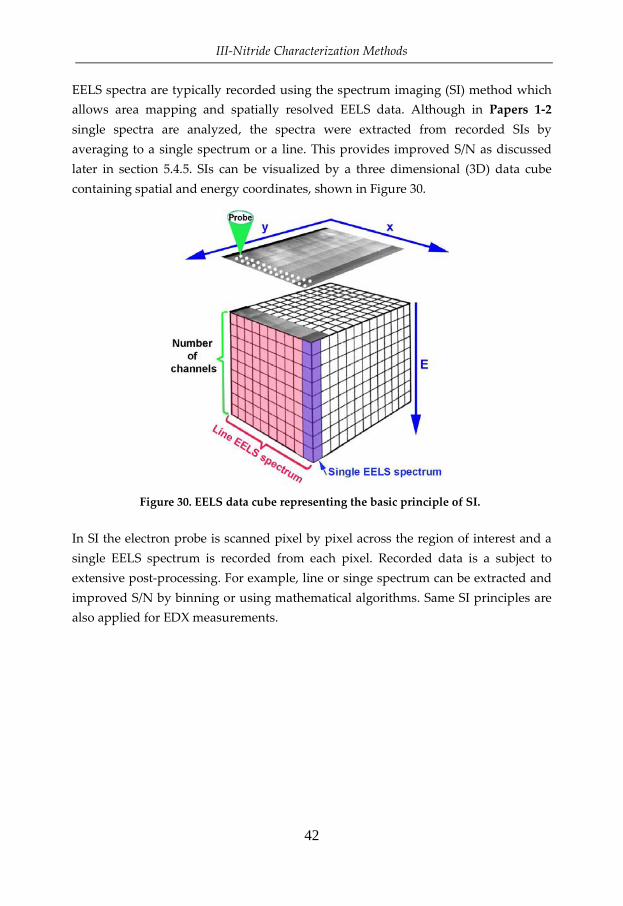
5.4 Electron Energy Loss Spectroscopy (EELS)
The EELS spectrometer is dedicated for measuring the amount of energy lost (∆E)
per electron in the primary beam (E0) as the electron interacts inelastically with the
sample (see Figure 27). The EELS spectrum can give insight into the composition,
bonding environment and properties of the sample under investigation [96-99].[96,97,98,99]The
TEM can be equipped with a spectrometer which is integrated into the column (in-
column filter) or mounted under the projection chamber (post-column filter). The
electrons entering the EELS spectrometer are dispersed by a magnetic prism
according to the amount of energy lost in the scattering process (see Figure 29).
Higher electron energy loss results in higher deflection angle. The EELS
spectrometer itself is a complex device containing a number of electromagnetic
lenses and deflectors, allowing precise manipulation and focusing of different
energy electrons onto the recording device [91].
The EELS spectrum is captured by a CCD camera, which records different energy
ranges depending on selected dispersion.
Figure 29. Working principle of a post-column EELS spectrometer.
III-Nitride Characterization Methods
41
Shape and intensity of the EELS spectrum is a characteristic of the elements present
in the investigated structure. There is a number of experimental parameters which
are essential for EELS measurements and data evaluation such as primary beam
energy (E0), energy spread of the primary beam (see Figure 32), convergence semi-
angle of the probe (α), acceptance semi-angle (β) of the spectrometer (see Figure 29),
energy dispersion of the spectrometer, probe size.
The primary beam energy is usually kept constant and is set by the acceleration
voltage of the microscope. The characteristic scattering cross-section and scattering
angle for different elements depends on E0. The energy spread of the primary beam
depends on the gun type and if a monochromator is available and in use. A small
energy spread is crucial for studying fine details of the EELS spectrum as well as a
reliable deconvolution process. The convergence semi-angle α of the probe
determines the angular range of electrons which contribute to the excitation of the
sample as well as the spatial resolution. α is set by the condenser apertures and
lenses. The acceptance semi-angle β defines angular range of electrons which can
enter the spectrometer. β is critical when evaluating the EELS spectrum since the
characteristic scattering angle of different elements is proportional to the energy loss.
Also, with increasing Z, the scattering angle increases. With well chosen β most of
the scattered signal will be collected and a high signal to noise (S/N) ratio will be
achieved. β can be controlled by acceptance apertures of EELS spectrometer and
camera length.
EELS experimental parameters are preferably kept constant for comparative
quantitative analysis. In this thesis, two instruments were used for performing
VEELS analysis with different sets of the experimental parameters which are
[116], interface abruptness [117], ultra-thin films [118], graphite [119], quasicrystals
[120], multilayers [121], nanowires [122,123], nanoparticles [124], and correlating
different physical properties at the nanometer scale [125].
III-Nitride Characterization Methods
45
This thesis concentrates exclusively on exploring the bulk plasmon properties as a
tool for material analysis and will be described in more detail.
The bulk plasmon peak in the EELS spectrum stems from the plasmon resonances,
that are excited in the material when the high energy electron beam interacts with
the weakly bound valence electrons. A simplified model of visualizing bulk plasmon
excitations is shown in Figure 33. The material is considered to be in equilibrium and
have ‘fixed’ atoms – ions and quasi-free electrons. The high energy electrons passing
though such material easily interact with the quasi-free electrons and distort the
equilibrium state by creating areas of excess positive and negative charges, which try
to compensate this imbalance and set themselves in collective oscillation motion. The
quasi-free electrons oscillating in the bulk produce the so called bulk plasmons,
which are treated as quasi-particles of certain energy.
Figure 33. Schematic illustration of distorted quasi-free electron plasma when high energy electrons pass through the material and generate volumes of positive and negative charge.
The energy of the bulk plasmon loss primarily depends on the valence electron
density. Bulk plasmon oscillations run through the crystal as a longitudinal
collective electron wave of loosely bound electrons with a characteristic frequency,
creating volumes of varying electron density. The plasmon oscillations are quickly
III-Nitride Characterization Methods
46
damped, in order of femtoseconds, and are localized to a few nm. The bulk plasmon
peak is the next most intense feature in the EELS spectrum (see Figure 31), providing
a strong signal which can be efficiently recorded and carries characteristic
information about the investigated material. Bulk plasmon loss electrons are
strongly scattered forwardly and, as a result of the narrower angular distribution,
even for a small acceptance angle most of the signal is easily collected.
Analyzing the intensity of the zero loss peak together with the intensity of the
inelastic scattering contribution, mainly from the low-loss EELS region, is a well
established and straightforward procedure to estimate the relative sample thickness.
Poisson statistics provide an expression for number of n (integers) plasmon
excitation probability (Pn) in a sample of the thickness (t):
�� � E�! QR;S� =&TU � �V�T , (15)
where In is the number of counts in the nth plasmon peak, It is the integrated number
of counts throughout plasmon spectrum, λ is the mean free path.
By setting n=0, a measurement of the inelastically scattered (low-loss region) versus
unscattered (zero-loss peak) intensities gives an indication of the sample thickness
by using the log-ratio method [75]. This is performed by taking ratios of the
integrated intensities of the entire spectrum and the zero-loss peak:
R; � WX �T�' , (16)
where t is the sample thickness, λ – the mean free path, IT – the integrated spectrum
area, and I0 is the area under the zero-loss peak.
Figure 34 shows a typical VEELS spectrum recorded from an AlN sample at
different thicknesses and normalized with respect to zero-loss intensity. With
developing sample thickness inelastic scattering contributions increase – the bulk
plasmon peak height increases. The sample thickness does not affect the position of
the bulk plasmon energy, hence more signal can be collected by recording VEELS
from thicker areas. Multiple scattering slightly affects the shape of the bulk plasmon
peak and, for data analysis, it should be removed by deconvolution procedures,
discussed more in detail in section 5.4.5.
III-Nitride Characterization Methods
47
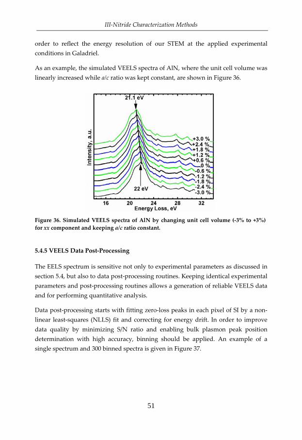
Figure 34. Low-loss EELS spectrum recorded from different thickness areas of AlN.
In order to describe the bulk plasmon energy, a mathematical description of valence
electron oscillations is given by the Drude model [21], which gives the free electron
plasma energy. In this model valence electrons are treated as free particles, and
damping in the electron plasma is not taken into account. The only parameter
influencing the plasma oscillations is the valence electron density. If the number of
valence electrons is constant, only the lattice parameter will affect the plasma
frequency. This model works well for metals.
In mathematical treatment [75,100,126], if the beam of high energy electrons is
considered as a time varying electric field which causes the ‘quasi-free’ electron
movements, the equation of motion must be satisfied:
� YZ#YRZ ��à Y#YR � �=�, (17)
where m is electron mass, x – displacement, Г – damping constant, e – electron
charge, and E – oscillation field.
For an oscillating local electric field, the solution of this equation is given by:
� � \]̂_Z`*Г_ , (18)
The ‘quasi-free’ electron displacement produces polarization in the medium:
� � �=X� � "IB� , (19)
where n is number of electrons per unit volume, and B – electronic susceptibility.
III-Nitride Characterization Methods
48
From the equation (19):
B � Ca@ Q E_Z`ГZ � &*Г_∙�_Z`ГZ�S . (20)
The response of the medium by the induced electric field is governed by the complex
dielectric response function:
" � "E � c"@ � 1 � B , (21)
where ε is the dielectric function, ε1 is its real part, and ε2 – imaginary part.
Electron losses can be described by differential cross-section characteristics of the
bulk loss function in the free electron approximation:
YZdYRZ ~lm?� Ef�g�D , (22)
where YZdYRZ is the differential cross-section.
In the free electron model the dielectric function of a material is given by:
"�C� � 1 � Ca Q E_Z`*Г_S , (23)
where ωp is the plasma frequency.
The frequency of the bulk plasmon oscillations according to the Drude model can be
expressed as:
Ca � h�iZj'k , (24)
where m is the electron effective mass, n – the valence electron density per unit
volume and .I – the permittivity of free space.
Forcing quasi-free electrons to oscillate is equivalent to creating a particle with
energy Ep:
�a � lCa . (25)
This model provides a reasonably accurate estimate of the plasma frequency for
many solids, except for transition metals and rare earth elements, due to their more
complex electronic structure.
III-Nitride Characterization Methods
49
However, in other crystals additional factors affect the appearance and shape of the
bulk plasmon energy such as band structure, momentum transfer, chemical bonds.
Moreover, a ‘plasmon’ response can be observed in insulators, showing that the
Drude model does not account for all phenomena present in materials. More
advanced Drude-Lorentz model, Lindhard models, and other approximations can be
used to account for additional factors mentioned above [126].
Alloying different elements alters the valence electron density in the system, which
affects the bulk plasmon peak shape and position. A peak shift in binary compounds
is commonly observed as linear empirical relation in the form:
�a��� � �a�0� � � QYmnY# S , (26)
where Ep(x) is bulk plasmon energy of the alloy, Ep(0) – bulk plasmon energy of the
one of the constituents, x – fraction of the alloy, and YmnY# – slope of linear dependence.
In Paper 1, a linear relation was experimentally established for the ternary AlxIn1-xN
system by investigating layers of different composition:
�a�HW#LXE&#o� � 14.78 � 5.69� . (27)
In Paper 2, it was demonstrated by a combination of experimental and simulations,
that the VEELS spectrum is affected by the strain state in group-III nitrides.
In Papers 3-5, VEELS was employed as the main tool for nanostructure
characterization on the nanoscale. High resolution bulk plasmon energy surface plot
of high-In content InGaN/GaN QW is shown in Figures 35. The dimensions
represent area (x,y) and Ep (z). The sharp onset of the well can be seen along with the
slower recovery and additional features inside QW (for more details see Paper 5).
In Papers 6-7, the decomposition processes and thermal stability of different
composition AlxIn1-xN layers and AlxIn1-xN/AlN multilayers were investigated by a
combination of monochromized VEELS, STEM imaging, and electron diffraction
during in-situ annealing from 750 oC to 950 oC.
III-Nitride Characterization Methods
50
Figure 35. Bulk plasmon energy surface plot of high-In content InGaN/GaN QW.
5.4.4 VEEL Spectrum Simulations
As discussed previously, VEELS provides complex information about the dielectric
response of a material, its composition and strain. For this reason, modeling is vital
in order to increase the understanding of experimental VEELS results [127]. To
retrieve the energy loss function and the optical properties of a material by
theoretical means, full potential simulations of the dielectric function can be
performed. One software package for such simulations is Wien2k, which is based on
quantum mechanics using density functional theory (DFT) [128], within the
generalized gradient approximation (GGA). In this package, the interaction between
electrons is treated as a series of one-electron Kohn-Sham partial differential
equations. The Wien2k simulation package employs the linearized augmented plane
wave (LAPW) method and has been established as one of the most exact methods to
compute the electronic structure of solids.
In Paper 2, Wien2k was employed to calculate effect of the strain on VEELS response
in AlN layers. The optical properties were calculated using the OPTIC subroutine in
Wien2k, which yields the dielectric function from which the energy-loss function is
obtained. Since AlN has the wurtzite structure which is anisotropic, the dielectric
function is described by a tensor. Because of this, two components (xx and zz) are
calculated simultaneously. For this investigation the xx component is of main
interest, as it is excited by the electron beam in the cross-sectional sample. For most
calculations of the loss function, a Gaussian broadening of only 0.1 eV was applied
to achieve a high level of detail in the energy-loss spectra. For final comparison of
the calculated and experimental spectra, a broadening of 1.0 eV was employed in
III-Nitride Characterization Methods
51
order to reflect the energy resolution of our STEM at the applied experimental
conditions in Galadriel.
As an example, the simulated VEELS spectra of AlN, where the unit cell volume was
linearly increased while a/c ratio was kept constant, are shown in Figure 36.
Figure 36. Simulated VEELS spectra of AlN by changing unit cell volume (-3% to +3%) for xx component and keeping a/c ratio constant.
5.4.5 VEELS Data Post-Processing
The EELS spectrum is sensitive not only to experimental parameters as discussed in
section 5.4, but also to data post-processing routines. Keeping identical experimental
parameters and post-processing routines allows a generation of reliable VEELS data
and for performing quantitative analysis.
Data post-processing starts with fitting zero-loss peaks in each pixel of SI by a non-
linear least-squares (NLLS) fit and correcting for energy drift. In order to improve
data quality by minimizing S/N ratio and enabling bulk plasmon peak position
determination with high accuracy, binning should be applied. An example of a
single spectrum and 300 binned spectra is given in Figure 37.
III-Nitride Characterization Methods
52
Figure 37. Comparison of a single spectrum and noise reduced spectrum obtained by averaging 300 spectra.
VEELS spectrum is preferably recorded from a sample where it can be treated as a
single scattering event; for bulk plasmons optimum is around 1 mean free path
thickness of the sample. Since in most cases, plural scattering contributions are still
present, VEELS spectrum must be deconvoluted by the Fourier-log method. This is
done by using routines available in the Digital Micrograph software. As typical for
all data treatment procedures, plural scattering removal routines should be used
with caution, since it can introduce artifacts in the spectrum, e.g., in the case of high
noise level. Finally, considering a single Gaussian function of the VEELS spectrum,
the bulk plasmon peak is again fitted by NLLS curve-fitting method in a ~2 eV
window centered around the most intense part of the plasmon peak in order to
determine the bulk plasmon energy (Figure 38).
Figure 38. Raw VEELS spectrum is deconvoluted from plural scattering and fitted with Gaussian shape peak to determine the exact bulk plasmon energy in AlN.
III-Nitride Characterization Methods
53
5.4.6 Core-Loss Region
The core-loss region (ionization edges with fine structure) contains information
carried by the electrons interacting with core shell electrons of a specimen atom,
causing their excitation to higher unoccupied levels, in the range from 50 eV up to
>>1000 eV. These excitations appear in the form of edges in the EELS spectrum. The
signal intensity compared to the low-loss region is weaker due to the smaller
ionization cross-section. As an example, characteristic N K-edge evolution in
different composition Al1-xInxN layers (0≤x≤1) is shown in Figure 39.
Figure 39. N (K-edge) of different composition Al1-xInxN layers.
The fine features of the spectra are sensitive to the Al1-xInxN alloy composition. The
fine structure of the edge provides information about the chemical environment of
the atoms. While the fine structure is usually significantly different, it can be used to
determine the compound (from a library of fine structures). Core-loss EELS is the
preferred technique for characterizing light elements present in the sample, like O, C
or N, etc.
III-Nitride Characterization Methods
54
5.5 In-Situ TEM Experiments
TEM provides capabilities to characterize samples with high spatial resolution
imaging together with reciprocal space and chemical information. This static analysis
is performed on samples which are synthesized or processed before they are
analyzed in TEM. Possibility to follow the sample evolution inside the microscope
under changing conditions enables the study of dynamic processes in materials with
high accuracy and provides additional information about the physical mechanisms
at the atomic level. The samples can be subjected to different triggers, such as
temperature, gas, strain, which will have an effect on the sample structure. This is
usually achieved by using dedicated specimen holders (annealing, indentation) or
specialized microscopes (environmental TEM). As a result, the sample will react to
the applied process and this can be followed live though imaging, diffraction and
spectroscopy techniques. The electron beam current effect on electron dose sensitive
materials can be regarded as the simplest in-situ TEM experiment.
In this thesis, in-situ annealing experiments were performed using a furnace type
double tilt heating holder (Gatan Model 652) shown in Figure 40. The heating holder
allows investigation of phase transformations, material disintegration, at
temperatures up to 1000 oC.
Figure 40. Double tilt heating holder tip.
Some concerns apply to high temperature annealing experiments. The sample
support material (grid) should withstand high temperature (titanium, molybdenum)
and not react with the heating furnace (tantalum). The same applies to the sample
itself. A high temperature glue (e.g., Gatan G1) must be used for traditional cross-
sectional sample preparation (section 5.6.1).
III-Nitride Characterization Methods
55
In Papers 6-7, the thermal stability and decomposition paths of Al1-xInxN layers were
investigated by STEM imaging, electron diffraction, and VEELS during in-situ
annealing from 750 oC to 950 oC. STEM images of Al0.3In0.7N/AlN multilayer structure
evolution during in-situ annealing experiment are shown in Figure 41a-d as time
series.
Figure 41. STEM images of AlInN/AlN multilayer evolution during in-situ annealing experiment.
III-Nitride Characterization Methods
56
5.6 TEM Sample Preparation
For bulk samples to be used in TEM analysis the thickness requirement is the most
critical, since sample must be electron transparent. This is achieved by reducing
sample dimensions from mm to μm and then to nm. Typical requirements for a
‘perfect’ TEM sample: thin over a large area, contains little or no artifacts from the
sample preparation process, represents the entire sample, clean and free from
contamination products, preferably conductive and non-magnetic. If the sample is
thick and has experienced considerable surface damage, dynamic scattering and
multiple interference might complicate the interpretation of the TEM results.
The choice of the sample preparation method depends on the sample itself (single
crystal, biological, nanoparticles, homogeneous etc.) and the desired projection (zone
axis). The typical zone axes in hexagonal crystals are parallel to the c-axis (plan-
view), and perpendicular to the c-axis (cross-section), see Figure 4.
Most TEM samples studied in this thesis were prepared conventionally by using
‘sandwich’ approach (few days of work). The major assumption done using this
method – the sample is homogeneous, since TEM sampling volume is rather small.
Detailed ‘sandwich’ approach procedure is illustrated in Figure 42. Initial sample (a)
is cut with low speed diamond saw into small 1.8 mm x 0.8 mm pieces (b) mounted
into Ti grid (c) which has standard 3 mm diameter fitting into microscope holder.
Figure 42. TEM sample preparation procedure: initial sample (a) cut to small pieces (b) and put in Ti grid (c) which is glued (d) polished and ion milled from both sides until final TEM sample (e) is ready, (f) overview TEM image from this sample.
The Ti grid is glued for ~2 h at 180 oC by using Arelite glue (d). In the case the
samples are subjected to in-situ annealing treatment, high temperature glue (G1)
should be chosen instead. The sample is mechanically polished by diamond
polishing papers with different grain sizes (e). The polishing is typically finished
III-Nitride Characterization Methods
57
when the sample thickness is ~50 μm. The final sample polishing is done by argon
ion milling (PIPS-Gatan) at 5 keV. The final step in milling is performed at low
energy (2 keV), which reduces the amorphous layer on the sample surface. After all
these treatment, sample is finally ready to be inspected in TEM (f).
5.6.2 TEM Samples in Few Minutes
TEM sample preparation is commonly accepted as long, joyful, and complicated
process. However, if the samples are in form of powder or nanostructures, like
nanorods – the TEM sample preparation is rather straightforward. Powder or
substrate-free nanorods (removed by scratching) are dispersed on Cu grid mesh
which contains amorphous carbon layer acting as support for particles. This type of
sample preparation was used to study individual AlInN nanorods in Papers 3-4.
5.6.3 Focused Ion Beam (FIB) Sample Preparation
FIB is another TEM sample preparation method applied in Paper 1 (B-series) and
Paper 4 (plan-view) by using FIB Carl Zeiss Cross-Beam 1540 EsB system. This
method was chosen since some samples were too small for conventional sample
preparation procedure.
The main advantage by using FIB is the selectivity of area from which the TEM
sample could be prepared. The FIB working platform is based on the scanning
electron microscope principle, with an additional Ga-ion column, which is used
mainly for sample milling and deposition. Gas injection system (GIS) is used for
depositing protective layer and manipulator is needed for sample lift-out (see Figure
43a). The disadvantage with FIB is that sample surface is affected by implanted Ga
ions. Additionally, FIB operation cost is rather high.
Standard FIB sample preparation procedure starts with identifying area of interested
by using SEM. This area is covered by e.g., platinum (Pt) layer where typical
thickness of Pt layer is around 1 μm. In order to lift out lamella protected by Pt,
trenches are milled using high ion current (~2 nA) around this lamella. For lift-out
procedure, a manipulator is inserted and welded to lamella by Pt (see Figure 43b).
Lamella is cut loose from the bulk sample and placed on half-moon Cu grid, where
the final thinning to electron transparency is performed.
III-Nitride Characterization Methods
58
Figure 43. (a) FIB system basic scheme and (b) SEM image of a sample ready for lift-out procedure.
III-Nitride Characterization Methods
59
5.7 Rutherford Backscattering Spectrometry (RBS)
Rutherford backscattering spectrometry is a routine technique for compositional
analysis on macroscopic scale of thin films [129]. The investigated material is
bombarded with high energy light ions (e.g., He), which are incident almost
perpendicular to the surface of the analyzed sample. The He ions interact with atoms
in the sample. Consequently, some ions are backscattered from the sample atoms
through elastic collisions. Compositional analysis is based on the interpretation of
the energy spectrum of backscattered ions through conservation of momentum. The
energy loss of backscattered ions depends on the elements present and the energy
dependent scattering cross-section. Experimental and simulated spectra of analyzed
Al0.66In0.34N sample are shown in Figure 44.
Figure 44. Experimental and simulated RBS spectra from Al0.66In0.34N sample grown on Al2O3 substrate with AlN buffer layer. In order to determine the elemental composition of the AlInN, 2.0 MeV 4He+ ions
were used at an incident angle of 7o off from the surface normal to avoid channeling
effects in the crystalline structure [130], and back-scattered 4He+ ions were detected
at a scattering angle of 172o. Experimental data was analyzed using the SIMNRA
code (version 6.05) [131] to obtain the exact film composition.
In Paper 1, the compositional information obtained by RBS was correlated with Ep
values and used for calibration as a function of alloy composition.
III-Nitride Characterization Methods
60
5.8 X-ray Diffraction (XRD)
X-ray diffraction is a result of the wave nature of X-rays (λ=1.54 Å, Cu Kα1), which
allows them to diffract and interfere constructively upon interacting with the
periodic structure of the crystal. As an example, the semiconductor crystal exhibits a
lattice periodicity of a few Å (a=3.11 Å and c=4.98 Å for AlN). Diffracted waves
provide information of the crystallographic structure, orientation, composition,
strain state, etc. of the materials [132-134].[132,133,134]Bragg’s law describes the condition for
constructive interference, i.e., the maximum intensity of scattered X-rays from the
crystal:
Xλ � 28sinx , (28)
where n is an integer number, λ – the wavelength, d – the lattice spacing and θ – the
diffraction angle.
Bragg’s law states that the maximum(-a) of the scattered intensity is(are) found
when the incident and scattered angles are θ for the periodic lattice spacing d (in the
crystal). Since λ and θ in an experimental setup are known, d can be calculated. This
is schematically illustrated in Figure 45. Fulfilling Bragg’s law is, however, not
enough for obtaining scattered intensity, since the scattering intensity is also related
to the structure factor of the investigated material. The structure factor takes into
account atomic positions and scattering powers in the unit cell, making some
reflections appear stronger, weaker or be completely forbidden.
Figure 45. The schematic principle of X-ray diffraction according to Bragg’s law is shown
in the HR-STEM image, indicating lattice spacing d as well as incident and diffraction
angles θ.
III-Nitride Characterization Methods
61
In the simplest XRD experiment incident and detection angles are varied
simultaneously and X-ray intensities recorded. This is the basis of a θ/2θ
measurement, which is a routine method for identifying crystal phases and
extracting lattice spacings parallel to the sample surface. As an example, a θ/2θ
measurement from Al0.24In0.76N(0002) grown on an AlN(0002) buffer layer is shown
in Figure 46, with distinct peaks representing different lattice parameters.
Figure 46. θ/2θ XRD measurement of Al0.24In0.76N(0002) grown on an AlN(0002) buffer layer.
In Paper 1, the c lattice parameters were obtained from θ/2θ XRD measurements and
were correlated with the bulk plasmon energy values and RBS compositional data.
In Paper 3, obtained c lattice parameter was used to estimate composition as
determined by Vegard’s rule using bulk AlN and InN lattice parameters [135].
In order to evaluate the crystal quality, strain, relaxation, coherency, in-plane and
out-of-plane lattice parameters, so called, reciprocal space maps (RSM), can be
recorded. RSM scans record continuously varying θ and ω to form an area image
around given reciprocal lattice points. The desired information is extracted from
position, shape and orientation of those reciprocal space peaks.
In Paper 2, the a and c lattice parameters were obtained from RSM measurement by
examining the symmetric (0002) and asymmetric (1015) reflections and were used to
estimate the unit cell volume and strain state of AlN layers grown on different
III-Nitride Characterization Methods
62
substrates and growth conditions. RSM representing the symmetric (0002) and
asymmetric (1015) reflections of AlInN multilayer samples are shown in Figure 47.
Figure 47. RSM from AlInN multilayer sample showing (0002) and (10��5) reciprocal lattice points.
Summary and Contribution to the Field
63
6. Summary and Contribution to the Field
The research presented in this thesis is focused on exploring and applying VEELS
capabilities for characterization of group III-nitride semiconductors with highest
spatial and energy resolution. VEELS is an indirect method to access the material
composition and strain: both experimental and theoretical investigations were
performed to obtain this information (Papers 1-2).
In the first study (Paper 1), a standard-free method to retrieve compositional
information of AlxIn1-xN thin films by employing STEM-VEELS was demonstrated.
Two series of samples were grown by MSE and MOCVD, covering together full
composition range 0≤x≤1. Complementary compositional measurements were
obtained using RBS and the lattice parameters were obtained by XRD. It was shown
that bulk plasmon energy follows a linear trend with respect to composition and lattice
parameter between the alloyed constituents from AlN to InN. This allows a
straightforward compositional analysis by a single measurement of the bulk
plasmon energy.
The effect of strain on the low-loss response of III-nitrides was evaluated
experimentally by STEM-VEELS and theoretically by full potential simulations using
Wien2k (Paper 2). Three AlN layers were grown by MSE using different growth
schemes. AlN layers were found in relaxed, tensile and compressive strained states
as was shown by RSM. The different strain states were the outcome of different
growth conditions with substrates, growth temperature and thickness. The tensile
strained AlN resulted in a red shift (-0.17 eV) of the bulk plasmon peak position,
while the compressively strained was blue shifted (+0.25 eV) with respect to the
strain-free AlN (20.46 eV). To support the experimental findings, a number of
simulations were performed, where the strain state of AlN as well as GaN and InN
was continuously changed. Experiments and simulations revealed that the bulk plasmon
peak position varies linearly with unit cell volume (0.156 eV per 1% volume change). It was
concluded that strain should be taken into account as an additional factor when
interpreting VEELS data.
The above methodology was applied in the investigation of confined structures such
as nanorods and InGaN/GaN QWs (Papers 3-5).
In Papers 3-4, spontaneously formed self-assembled AlInN core–shell nanorods and
twisted nanorods were realized by MSE method. The grown structures exhibited
hexagonal cross-sections with preferential growth of the c-axis along the rod-length
Summary and Contribution to the Field
64
direction. The microstructure and compositional homogeneity in cross-sectional and
plan-view geometries were examined by STEM-VEELS and EDX mapping. The
compositional analysis showed higher In concentration in the core of the nanostructures than
in the surrounding shell, revealing phase separation which occurred during the growth.
The early stages of InxGa1-xN/GaN QW growth for In-reduced conditions were
investigated in Paper 5. The QW thickness and composition was varied during the
growth. The high spatial resolution analytical information was obtained by
monochromated STEM-VEELS spectrum imaging. It was found that QW beyond a
critical thickness (> 8 nm) and composition (x > 0.08) develop QD like features inside the
well as a consequence of Stranski-Krastanov-type growth mode, and QDs were buried by
continued growth of GaN while residual In was incorporated in the structure.
Finally, the thermal stability and degradation mechanisms of Al1-xInxN layers with
different In content and different periodicity AlInN/AlN layers were investigated
(Papers 6-7).
In Paper 6, the thermal stability of Al1-xInxN (0≤x≤1) layers was investigated by
combination of STEM imaging, monochromated VEELS and electron diffraction
during in-situ annealing from 750 oC to 950 oC. The results show two distinct
decomposition paths for the In-richest layers that independently lead to transformation of the
layers into a porous, nanocrystalline, In-deficient structure. The In-richest layer
(Al0.28In0.72N) decomposes at 750 oC, and the decomposition process is initiated by
forming In clusters at the grain boundaries. VEELS mapping clearly indicated
clustering of In with the presence of a sharp resonance peak at 11.4 eV. For the
Al0.41In0.59N layer, continues In desorption was initiated at 800 oC, while no In clusters
were observed. Al-rich Al1-xInxN layers resisted the thermal annealing.
Paper 7 reports the spinodal decomposition, as observed in-situ by STEM-VEELS,
during thermal annealing in AlxIn1-xN/AlN multilayer films with original
composition inside the miscibility gap. The original layers were grown by MSE at
room temperature, which suppressed the decomposition into a metastable state. It
was found that the decomposition process initially occurs by surface directed spinodal
decomposition. The poor thermal stability of the formed In-rich domains was further
confirmed by the desorption of In from the layers, from the surface of the thin TEM
cross-sectional samples, while In was also found to diffuse into the ambient AlN.
65
Bibliography
7. Bibliography [1] R. E. Homel ‘Understanding material science: history, properties, applications’
(Springer, New York, 2004).
[2] C. Blatchford‘Many ways of hearing: 94 multitasked lessons in listening’ (J.
Weston Walch, 1997).
[3] I.N. Prassiankis ‘Quality control of materials in Acient Greece using non
Chen & C.-H. Chen ‘Anisotropic surface plasmon excitation in Au/silica
nanowire’ Appl. Phys. Lett. 96, 263106 (2010).
[114] A. L. Koh, K. Bao, I. Khan, W. E. Smith, G. Kothleitner, P. Nordlander, S. A.
Maier & D. W. McComb ‘Electron energy-loss spectroscopy (EELS) of surface
plasmons in single silver nanoparticles and dimers: influence of beam damage
and mapping of dark modes’ ACS Nano 3, 3015 (2009).
[115] M. Bosman, V. J. Keast, M. Watanabe, A. I. Maaroof & M. B. Cortie ‘Mapping
surface plasmons at the nanometer scale with an electron beam’
Nanotechnology 18, 165505 (2007).
[116] M. Benaissa, L. Gu, M. Korytov, T. Huault, P. A. van Aken, J. Brault & P.
Vennegues ‘Phase separation in GaN/AlGaN quantum dots’ Appl. Phys. Lett.
95, 141901 (2009).
[117] L. H. Tizei, T. Chiaramonte, M. A. Cotta & D. Ugarte ‘Characterization of
interface abruptness and material properties in catalytically grown III-V
73
Bibliography
nanowires: exploiting plasmon chemical shift’ Nanotechnology 23, 295701
(2010).
[118] D. Su, B. Yang, N. Jiang, M. Sawicki, C. Broadbridge, M. Couillard, J. W.
Reiner, F. J. Walker, C. H. Ahn & Yimei Zhu ‘Valence electron energy-loss
spectroscopy of ultrathin SrTiO3 films grown on silicon (100) single crystal’
Appl. Phys. Lett. 96, 121914 (2010).
[119] T. Eberlein, U. Bangert, R. R. Nair, R. Jones, M. Gass, A. L. Bleloch, K. S.
Novoselov, A. Geim & P. R. Briddon ’Plasmon spectroscopy of free-standing
graphene films’ Phys. Rev. B 77, 233406 (2008).
[120] T. Grenet & M.C. Cheynet ‘Plasmons in icosahedral quasicrystals: An EELS
investigation’ Eur. Phys. J. B 13, 701 (2000).
[121] M.A. M. Yajid & G. Mobus ‘Reactive multilayers examined by HRTEM and
plasmon EELS chemical mapping’ Microsc. Microanal. 15, 54, (2009).
[122] J. Wang, Q. Li, C. Ronning, D. Stichtenoth, S. Muller & D. Tang ‘Nanomaterial
electronic structure investigation by valence electron energy loss spectroscopy-
an example of doped ZnO nanowires’ Micron 39, 703 (2008).
[123] D. Rossouw, M. Couillard, J. Vickery, E. Kumacheva & G. A. Botton
‘Multipolar plasmonic resonances in silver nanowire antennas imaged with a
sub-nanometer electron probe’ Nano Lett. 11, 1499 (2011).
[124] N. Jiang, D. Su, J. C.H. Spence, S. Zhou & J. Qiu ‘Volume plasmon of bismuth
nanoparticles’ Solid State Commun. 149, 111 (2009).
[125] L. Gu, V. B. Ozdol, W. Sigle, C. T. Koch, V. Srot & P. A. van Aken ‘Correlating
the structural, chemical, and optical properties at nanometer resolution’ J.
Appl. Phys. 107, 013501 (2010).
[126] R.F. Egerton ‘Electron energy loss spectroscopy in the electron microscope’
(Springer, New York, 2011).
[127] V.J. Keast ‘Ab-Initio calculations of plasmons and interband transitions in the low-loss electron energy-loss spectrum’ J. Electron. Spectrosc. Relat. Phenom 143, 97 (2005).
[128] K. Schwarz & P. Blaha ‘Solid state calculations using WIEN2k’ Comput. Mater.
Sci. 28, 259 (2003).
[129] J. R. Tesmer & M. A. Nastasi ‘Handbook of Modern Ion Beam Materials
Analysis’ (Materials Research Society, Pittsburgh, 1995).
[130] K. Lorenz, N. Franco, E. Alves, I. M. Watson, R. W. Martin & K. P. O’Donnell
‘Anomalous ion channeling in AlInN/GaN bilayers: determination of the strain
state’ Phy. Rev. Lett 97, 085501 (2006).
74
Bibliography [131] M. Mayer ’SIMNRA- the simulation of backscattering spectra software’
http://www.simnra.com (2012-10-07).
[132] B. D. Cullity ‘Elements of X-ray diffraction’ (Prentice Hall, New Jersey, 2001).
[133] B. E. Warren ‘X-ray diffraction’ (Dover Publications, New York, 1990).
[134] M. A. Moram & M. E. Vickers ‘X-ray diffraction of III-nitrides’ Rep. Prog. Phys.
72, 036502 (2009).
[135] K. Kubota, Y. Kobayashi & K. Fujimoto ‘Preparation and properties of III-V
nitride thin films’ J. Appl. Phys. 66, 2984 (1989).